KR20140143679A - Digitizer - Google Patents
DigitizerDownload PDFInfo
- Publication number
- KR20140143679A KR20140143679AKR1020130142772AKR20130142772AKR20140143679AKR 20140143679 AKR20140143679 AKR 20140143679AKR 1020130142772 AKR1020130142772 AKR 1020130142772AKR 20130142772 AKR20130142772 AKR 20130142772AKR 20140143679 AKR20140143679 AKR 20140143679A
- Authority
- KR
- South Korea
- Prior art keywords
- voltage
- output
- analog
- digitizer
- outputting
- Prior art date
- Legal status (The legal status is an assumption and is not a legal conclusion. Google has not performed a legal analysis and makes no representation as to the accuracy of the status listed.)
- Ceased
Links
Images


Classifications
- G—PHYSICS
- G06—COMPUTING OR CALCULATING; COUNTING
- G06F—ELECTRIC DIGITAL DATA PROCESSING
- G06F3/00—Input arrangements for transferring data to be processed into a form capable of being handled by the computer; Output arrangements for transferring data from processing unit to output unit, e.g. interface arrangements
- G06F3/01—Input arrangements or combined input and output arrangements for interaction between user and computer
- G06F3/03—Arrangements for converting the position or the displacement of a member into a coded form
- G06F3/041—Digitisers, e.g. for touch screens or touch pads, characterised by the transducing means
- G06F3/046—Digitisers, e.g. for touch screens or touch pads, characterised by the transducing means by electromagnetic means
Landscapes
- Engineering & Computer Science (AREA)
- Physics & Mathematics (AREA)
- General Engineering & Computer Science (AREA)
- Theoretical Computer Science (AREA)
- Electromagnetism (AREA)
- Human Computer Interaction (AREA)
- General Physics & Mathematics (AREA)
- Position Input By Displaying (AREA)
Abstract
Translated fromKoreanDescription
Translated fromKorean본 발명은 디지타이저에 관한 것으로, 루프센서에서 차동증폭기를 통해 출력된 전압의 축적을 통해 전압을 증폭하고, 증폭된 전압에서 노이즈를 제거하여 최종 좌표 출력을 빠르게 하고 정밀도를 높일 수 있도록 한 디지타이저에 관한 것이다.
BACKGROUND OF THE
디지타이저 시스템을 구현함에 있어서, 좌표 데이터를 부여하기 위한 태블릿(tablet), 태블릿에 의해 표현된 좌표계의 한 점을 지정하기 위한 스타일러스, 핑거 등의 포인팅 디바이스, 그리고 이들을 제어하기 위한 디지타이저 컨트롤러가 필요하다.In implementing the digitizer system, a tablet for giving coordinate data, a stylus for designating a point in the coordinate system expressed by the tablet, a pointing device such as a finger, and a digitizer controller for controlling them are required.
디지타이저는 키보드나 마우스와 같은 입력 장치와 달리, 화면 상에서 사용자가 지시한 위치 정보를 입력받는 장치이다. 이에 따라, 캐드와 같은 그래픽 작업을 수행하기에 적합하며, 직관적이고 편리한 사용자 인터페이스를 제공하기 위해 많이 사용되고 있다.A digitizer is a device that receives position information indicated by a user on a screen, unlike an input device such as a keyboard or a mouse. Accordingly, it is suitable for performing graphic work such as CAD, and is widely used for providing an intuitive and convenient user interface.
이와 같은 디지타이저는 터치스크린, EGIP(Electric graphic input panel)라고 불리기도 하며, 사용자가 지시한 위치를 검출하는 방식에 따라 크게 저항막(Resistive) 방식, 정전용량(Capacitive) 방식, 전자기 공명(ElectroMagnetic Resonance, EMR)방식(혹은 전자기 방식) 등으로 분류된다.Such a digitizer is also referred to as a touch screen or an electric graphic input panel (EGIP). Depending on a method of detecting a position pointed by a user, the digitizer is largely classified into a resistive method, a capacitive method, an electromagnetic resonance , EMR method (or electromagnetic method), and the like.
저항막 방식은 직류 전압을 인가한 상태에서 압력에 의해 눌려진 위치를 전류량의 변화에 의해 감지하는 방식으로써, 스크린 위에 두 층의 얇은 도전층이 손가락 또는 스타일러스 펜에 의한 압력에 의해 직접 접촉이 되는 것을 감지한다.The resistance film method is a method in which a position pressed by a pressure in the state of applying a direct current voltage is detected by a change in the amount of current, and a thin conductive layer of two layers is directly contacted with a finger or a stylus pen Detection.
저항막 방식은 압력에 의해 위치를 감지하기 때문에 감지의 대상이 도체 또는 부도체인지 여부와 상관이 없다.Since the resistance film method detects the position by the pressure, it does not matter whether the object to be sensed is a conductor or a bank.
정전용량 방식은 교류전압을 인가한 상태에서 커패시턴스 커플링(Capacitance Coupling)을 이용하여 감지하는 방식으로써, 감지의 대상이 반드시 도체이어야 하고 감지 가능한 정전용량의 변화를 주기위해 일정 이상의 접촉면적이 필요하다. 따라서 정전용량 방식의 경우에는 사람의 손가락을 이용하여 입력 시에는 위치 감지에 문제가 없으나 도체 팁 형태의 경우 접촉 면적이 작아 감지가 어려운 특징이 있다.The capacitive method is a method of detecting by using capacitance coupling in the state of applying an AC voltage. The object to be sensed must be a conductor and a contact area of more than a certain level is required to change the sensible capacitance . Therefore, in the case of the capacitive type, there is no problem in the position sensing at the time of input using the human finger, but in the case of the conductive tip type, the contact area is small and the detection is difficult.
한편, 전자기 공명 방식은 복수개의 코일을 포함한 디지타이저 센서 기판을 이용하며, 사용자가 펜을 움직이면, 펜이 진동하는 자계를 일으키도록 교류신호에 의하여 구동되며, 진동하는 자계는 코일에 신호를 유도하고, 코일에 유도된 신호를 통해 펜의 위치를 검출한다.On the other hand, the electromagnetic resonance method uses a digitizer sensor substrate including a plurality of coils. When a user moves the pen, the pen is driven by an AC signal so as to cause a magnetic field to vibrate. The vibrating magnetic field induces a signal to the coil, The position of the pen is detected through a signal induced in the coil.
이와 같이 전자기 방식은 디지타이저 기판에 다수개의 코일을 장착하고, 펜의 접근에 의해 발생하는 전자기적 변화를 감지하여 펜의 위치를 파악한다.In this way, the electromagnetic system mounts a plurality of coils on the digitizer substrate, and detects the electromagnetic change caused by the approach of the pen to grasp the position of the pen.
이하 첨부된 도면을 참조하여 종래 기술에 따른 디지타이저 및 그의 노이즈 제거 방법을 설명하기로 한다.DETAILED DESCRIPTION OF THE PREFERRED EMBODIMENTS Hereinafter, a digitizer and a noise removing method according to the related art will be described with reference to the accompanying drawings.
도 1은 종래 기술에 따른 디지타이저를 설명하기 위한 블록 구성도이고, 도 2는 도 1에 나타낸 전단부를 상세히 나타낸 도면이다.FIG. 1 is a block diagram illustrating a digitizer according to the related art, and FIG. 2 is a detailed view of a front end portion shown in FIG.
종래 기술에 따른 디지타이저는 대한민국 특허청에 10-1006877호로 특허 등록된 투명 디지타이저로써, 이러한 디지타이저는 디스플레이 스크린 호스트 장치(10)에 적용된다.The digitizer according to the prior art is a transparent digitizer registered as a patent 10-1006877 in the Korean Intellectual Property Office. Such a digitizer is applied to the display
디지타이저는 그리드에 기초한 센서(12)를 포함하는데, 이것은 투명하게 하는 것이 바람직하고 또한 FPD(14)의 상부에 위치한다. 아날로그 전단부 ASIC(16)들이 바람직하게 는 센서의 프레임 상에 장착된다. 상기 ASIC은 바람직하게는 다음에 더 상세하게 기술되는 것과 같은 그리드로된 여러 가지의 전도체들의 출력에 연결된다. 각각의 전단부(front-end)는 센서 도체에 의해 출력되는 매우 낮은 진폭의 신호들을 수신한다.The digitizer includes a grid-based
상기한 ASIC(16)은 신호를 증폭하고, 부적절한 주파수들을 식별해 걸러내며, 출력을 디지털 형태로 샘플링하고, 샘플화 된 데이터를 데이터 버스(18)로 전송하여 디지털 프로세싱 유닛(20)에서 후속처리를 하도록 구성한다. 디지털 프로세싱 유닛(20)은 다양한 디지털 프로세싱 알고리즘을 수행한다.The ASIC 16 amplifies the signal, identifies and filters out the improper frequencies, samples the output in digital form, and sends the sampled data to the
유닛(20)에 의해 수행되는 디지털 프로세싱의 결과는 바람직하게는 하나 또는 다수의 물리적 물체들의 위치, 전형적으로는 스타일러스의 위치에 해당하고, 그 결과는 일단 결정되면 인터페이스(24)를 통해 호스트(22)로 전송되어 어플리케이션에 의한 프로세싱을 받게 된다.The result of the digital processing performed by the
디지털 프로세싱 유닛(20)의 부가적인 임무는 센서 배열장치와 디스플레이 스크린을 에워싸는 여기 코일(26)에 제공될 트리거링 펄스를 생성하고 관리하는 것이다. 여기 코일은 후속적으로 검출될 수 있는 스타일러스로부터 응답을 제공토록 하기 위해 스타일러스의 패시브 회로를 여기하는 트리거 펄스를 제공한다.An additional task of the
한편, 도 2에 나타낸 바와 같이, 전단 유닛(16)은 일련의 차동증폭기들(60.1 내지 60.n)을 포함한다. 차동 증폭기들은 스위치들(62.1 내지 62.m)에 그룹으로 연결된다. 상기 스위치들은 연결된 증폭기들 중의 하나로부터 다음 단으로 신호들을 전달한다. 또한 상기 스위치들은 차례로 필터와 증폭회로(64.1 내지 64.m), 그리고 A/D 컨버터들(66.1 내지 66.m)에 연결된다. A/D 컨버터들은 출력 버퍼(68)에 연결되고, 디지털 프로세싱 유닛을 위한 최종적인 출력 신호를 생성한다.On the other hand, as shown in Fig. 2, the
각각의 차동증폭기들(60.1 내지 60.n)은 바람직하게는 그의 차동 입력단 각각을 통해 그리드의 센서들 중의 다른 하나에 연결된다. 차동증폭기에 접속된 두개의 센서들은 바람직하게는 인접하는 센서들은 아니며 각각의 센서 신호들은 따라서 두 센서들 간의 차이를 나타내는 신호들로 변환된다.Each of the differential amplifiers 60.1 to 60.n is preferably connected to the other one of the sensors of the grid via each of its differential input stages. The two sensors connected to the differential amplifier are preferably not adjacent sensors, and each sensor signal is thus converted into signals indicative of the difference between the two sensors.
차동 신호는 증폭되어 스위치(62)에 전달된다. 각각의 스위치는 네 개의 증폭기들 사이에 접속되어 후속하여 처리될 네 개의 이용 가능한 증폭기 입력들 중의 하나를 선택한다. 상기 선택된 신호는 증폭되어 필터 및 증폭기(64)에 의해 필터링 되어, 그 다음 A/D 컨버터(66)에 의해 샘플링 된다. 디지털화 된 샘플 값은 그 다음 버퍼(68)에 전송되어 프로세싱 유닛으로 보내진다.The differential signal is amplified and transmitted to the switch 62. Each switch is connected between four amplifiers to select one of four available amplifier inputs to be processed subsequently. The selected signal is amplified and filtered by a filter and amplifier 64 and then sampled by an A / D converter 66. The digitized sample value is then sent to the
각각의 전단부 ASIC는 두 개의 동일한 채널들을 구비하며, 그 각각은 네 개의 차동 입력단들을 처리하며, 따라서 도면들의 참조기호에 있어서 n = 8 및 m = 2이다. 그러한 ASIC은 두 개의 A/D 컨버터들과, 두 개의 필터 및 증폭기 유닛과, 두 개의 스위치들 및 8개의 차동 증폭기를 구비한다.
Each front-end ASIC has two identical channels, each of which processes four differential inputs, thus n = 8 and m = 2 for reference symbols in the figures. Such an ASIC comprises two A / D converters, two filter and amplifier units, two switches and eight differential amplifiers.
그러나 이와 같은 종래 기술에 있어서는 다음과 같은 문제가 있었다.However, such conventional techniques have the following problems.
첫째, 노이즈를 제거하기 위해서 스캐닝을 여러 번 하여 평균치 값을 연산에 이용하여야만 했다. 이와 같이 동일 센서에 여러 번 스캐닝하는 경우, 전체 프로세싱 시간이 증가하게 되는데, 각각의 센서에 차동 증폭기 삽입하여, 노이즈 제거 면에서는 좋지만, 로직이 아주 복잡하다는 문제가 있었다.First, in order to remove the noise, several times of scanning have been used to calculate the average value. When the same sensor is scanned several times, the total processing time is increased. A differential amplifier is inserted into each sensor, which is good in terms of noise reduction, but the logic is very complicated.
둘째, 차동증폭기의 개수가 센서의 개수만큼 구성되므로 디지타이저 면적이 커지고, 생산 비용이 증가하였다.
Second, since the number of differential amplifiers is equal to the number of sensors, the digitizer area increases and the production cost increases.
따라서, 본 발명은 상기와 같은 종래 기술의 제반 단점과 문제점을 해결하기 위한 것으로, 본 발명은 루프센서에서 차동증폭기를 통해 출력된 전압의 축적을 통해 전압을 증폭하고, 증폭된 전압에서 노이즈를 제거하여 최종 좌표 출력을 빠르게 하고 정밀도를 높일 수 있도록 한 디지타이저를 제공하는데 그 목적이 있다.SUMMARY OF THE INVENTION Accordingly, the present invention has been made to solve the above problems and disadvantages of the related art, and it is an object of the present invention to provide a loop sensor which amplifies a voltage through accumulation of a voltage output through a differential amplifier, And to provide a digitizer capable of speeding up final coordinate output and increasing precision.
본 발명의 다른 목적들은 이하의 실시예에 대한 설명을 통해 쉽게 이해될 수 있을 것이다.
Other objects of the present invention will become readily apparent from the following description of the embodiments.
상기한 목적을 달성하기 위한 본 발명 디지타이저는 스타일러스 펜의 접근을 센싱하는 복수의 루프센서(110); 복수의 루프센서(110)의 센싱 데이터를 선택적으로 스위칭하여 출력하는 아날로그 스위칭부(120); 아날로그 스위칭부(120)의 출력을 증폭하여 출력하는 차동증폭부(130); 차동증폭부(130)의 출력전압을 축적하는 전압축적부(140); 전압축적부(140)에서 축적되어 출력되는 전압을 아날로그 디지털 변환하여 출력하는 아날로그 디지털 변환부(150); 및 아날로그 디지털 변환부(150)에서 출력된 데이터에서 루프센서(110)가 센싱한 좌표를 연산하는 제어부(160);를 포함하여 구성됨을 특징으로 한다.
According to an aspect of the present invention, there is provided a digitizer comprising: a plurality of loop sensors for sensing an approach of a stylus pen; An
이상에서 설명한 바와 같이, 본 발명에 의한 디지타이저에 의하면 다음과 같은 효과가 있다.As described above, the digitizer according to the present invention has the following effects.
첫째, 소프트웨어를 이용한 여러 번의 스캔에 의해서 노이즈를 제거하는 방식에 비하여, 하드웨어인 전압축적장치를 통해서 전압을 증폭하고, 노이즈를 제거 할수 있어 추가적인 소프트웨어 계산이 필요하지 않아 최종 좌표을 빠를게 출력 할수 있다. 즉 리포팅 타임을 줄일 수 있다.First, the voltage can be amplified through the hardware voltage accumulator and the noise can be eliminated, so that no additional software calculation is required, so that the final coordinates can be outputted quickly. That is, the reporting time can be reduced.
둘째, 작은 전압량을 전압 축적기를 통해서 크게 증폭할 수 있으며, 그에 따라 좌표의 정밀도를 향상 시킬 수 있다.Second, the small voltage amount can be greatly amplified through the voltage accumulator, thereby improving the accuracy of the coordinates.
도 1은 종래 기술에 따른 디지타이저를 설명하기 위한 블록 구성도이다.
도 2는 도 1에 나타낸 전단부를 상세히 나타낸 도면이다.
도 3은 본 발명에 따른 디지타이저의 구성을 설명하기 위한 도면이다.
도 4 내지 도 5는 도 3에 나타낸 전압축적장치(Voltage Accumulator)를 설명하기 위한 도면이다.
도 6은 도 4 내지 도 5에 나타낸 전압축적장치의 동작을 설명하기 위한 도면이다.1 is a block diagram illustrating a digitizer according to the related art.
Fig. 2 is a detailed view of the front end portion shown in Fig. 1. Fig.
3 is a diagram for explaining a configuration of a digitizer according to the present invention.
FIGS. 4 to 5 are diagrams for explaining a voltage accumulator shown in FIG. 3. FIG.
FIG. 6 is a view for explaining the operation of the voltage accumulating device shown in FIGS. 4 to 5. FIG.
본 발명은 다양한 변경을 가할 수 있고 여러 가지 실시예를 가질 수 있는 바, 특정 실시예들을 도면에 예시하고 상세한 설명에 상세하게 설명하고자 한다. 그러나, 이는 본 발명을 특정한 실시 형태에 대해 한정하려는 것이 아니며, 본 발명의 사상 및 기술 범위에 포함되는 모든 변경, 균등물 내지 대체물을 포함하는 것으로 이해되어야 한다.While the invention is susceptible to various modifications and alternative forms, specific embodiments thereof are shown by way of example in the drawings and will herein be described in detail. It should be understood, however, that the invention is not intended to be limited to the particular embodiments, but includes all modifications, equivalents, and alternatives falling within the spirit and scope of the invention.
각 도면을 설명하면서 유사한 참조부호를 유사한 구성요소에 대해 사용하였다. 본 발명을 설명함에 있어서 관련된 공지 기술에 대한 구체적인 설명이 본 발명의 요지를 흐릴 수 있다고 판단되는 경우 그 상세한 설명을 생략한다.Like reference numerals are used for like elements in describing each drawing. DETAILED DESCRIPTION OF THE PREFERRED EMBODIMENTS Hereinafter, the present invention will be described in detail with reference to the accompanying drawings.
제1, 제2 등의 용어는 다양한 구성 요소들을 설명하는데 사용될 수 있지만, 상기 구성 요소들은 상기 용어들에 의해 한정되어서는 안된다. 상기 용어들은 하나의 구성요소를 다른 구성요소로부터 구별하는 목적으로만 사용된다.The terms first, second, etc. may be used to describe various elements, but the elements should not be limited by the terms. The terms are used only for the purpose of distinguishing one component from another.
예를 들어, 본 발명의 권리 범위를 벗어나지 않으면서 제1 구성요소는 제2 구성요소로 명명될 수 있고, 유사하게 제2 구성요소도 제1 구성요소로 명명될 수 있다.For example, without departing from the scope of the present invention, the first component may be referred to as a second component, and similarly, the second component may also be referred to as a first component.
및/또는 이라는 용어는 복수의 관련된 기재된 항목들의 조합 또는 복수의 관련된 기재된 항목들 중의 어느 항목을 포함한다.And / or < / RTI > includes any combination of a plurality of related listed items or any of a plurality of related listed items.
어떤 구성요소가 다른 구성요소에 "연결되어" 있다거나 "접속되어" 있다고 언급된 때에는, 그 다른 구성요소에 직접적으로 연결되어 있거나 또는 접속되어 있을 수도 있지만, 중간에 다른 구성요소가 존재할 수도 있다고 이해되어야 할 것이다.It is to be understood that when an element is referred to as being "connected" or "connected" to another element, it may be directly connected or connected to the other element, .
반면에, 어떤 구성요소가 다른 구성요소에 "직접 연결되어" 있다거나 "직접 접속되어" 있다고 언급된 때에는, 중간에 다른 구성요소가 존재하지 않는 것으로 이해되어야 할 것이다.On the other hand, when an element is referred to as being "directly connected" or "directly connected" to another element, it should be understood that there are no other elements in between.
본 출원에서 사용한 용어는 단지 특정한 실시예를 설명하기 위해 사용된 것으로, 본 발명을 한정하려는 의도가 아니다.The terminology used in this application is used only to describe a specific embodiment and is not intended to limit the invention.
단수의 표현은 문맥상 명백하게 다르게 뜻하지 않는 한, 복수의 표현을 포함한다. 본 출원에서, "포함하다" 또는 "가지다" 등의 용어는 명세서상에 기재된 특징, 숫자, 단계, 동작, 구성요소, 부품 또는 이들을 조합한 것이 존재함을 지정하려는 것이지, 하나 또는 그 이상의 다른 특징들이나 숫자, 단계, 동작, 구성요소, 부품 또는 이들을 조합한 것들의 존재 또는 부가 가능성을 미리 배제하지 않는 것으로 이해되어야 한다.The singular expressions include plural expressions unless the context clearly dictates otherwise. In the present application, the terms "comprises" or "having" and the like are used to specify that there is a feature, a number, a step, an operation, an element, a component or a combination thereof described in the specification, But do not preclude the presence or addition of one or more other features, integers, steps, operations, elements, components, or combinations thereof.
다르게 정의되지 않는 한, 기술적이거나 과학적인 용어를 포함해서 여기서 사용되는 모든 용어들은 본 발명이 속하는 기술 분야에서 통상의 지식을 가진 자에 의해 일반적으로 이해되는 것과 동일한 의미를 가지고 있다.Unless defined otherwise, all terms used herein, including technical or scientific terms, have the same meaning as commonly understood by one of ordinary skill in the art to which this invention belongs.
일반적으로 사용되는 사전에 정의되어 있는 것과 같은 용어들은 관련 기술의 문맥상 가지는 의미와 일치하는 의미를 가지는 것으로 해석되어야 하며, 본 출원에서 명백하게 정의하지 않는 한, 이상적이거나 과도하게 형식적인 의미로 해석되지 않는다.Terms such as those defined in commonly used dictionaries are to be interpreted as having a meaning consistent with the contextual meaning of the related art and are to be interpreted as either ideal or overly formal in the sense of the present application Do not.
이하의 설명에서 종래의 디지타이저와 비교하여 종래의 디지타이저에 포함되어 이용되는 기술적 내용은 당업자에게 자명한 사항으로서 설명을 생략하고, 본 발명의 특징만을 중심으로 본 발명의 바람직한 일 실시예에 따른 디지타이저에 대해 설명하기로 한다.In the following description, the technical contents used in the conventional digitizer as compared with the conventional digitizer will not be described as obvious to those skilled in the art, and the digitizer according to the preferred embodiment of the present invention, Will be described.
그리고 일반적으로 디지타이저라 하면 펜을 이용하여 데이터를 입력할 수 있는 장치로서, 펜과 펜이 접촉하게 되는 장치인 타블렛으로 구성된다.In general, a digitizer is a device for inputting data by using a pen, which is composed of a tablet, which is a device in which a pen and a pen are brought into contact with each other.
그러나 일반적으로 이를 서로 구별하여 사용하지 않고 타블렛만을 가리켜 디지타이저라 하기도 하고, 펜과 타블렛을 모두 포함하여 디지타이저라 칭하기도 하는바 이하에서는 특별한 구분없이 혼용하여 사용하기로 한다.
In general, however, the tablet may be referred to as a digitizer without distinguishing the tablet from the tablet, and may be referred to as a digitizer including both a pen and a tablet.
도 3은 본 발명에 따른 디지타이저의 구성을 설명하기 위한 도면이다.3 is a diagram for explaining a configuration of a digitizer according to the present invention.
본 발명에 따른 디지타이저는 복수의 루프센서(110), 아날로그 스위칭부(120), 차동증폭부(130), 전압축적부(140), 아날로그 디지털 변환부(150) 및 제어부(160)를 포함하여 구성된다.The digitizer according to the present invention includes a plurality of
여기서, 복수의 루프센서(110)는 스타일러스 펜의 접근을 센싱한다.Here, the plurality of
아날로그 스위칭부(120)는 복수의 루프센서(110)의 센싱 데이터를 선택적으로 스위칭하여 출력한다. 이러한 아날로그 스위칭부(120)는 루프센서(100)를 자유롭게 차동증폭부(130)에 연결할수 있도록 한다.The
차동증폭부(130)는 아날로그 스위칭부(120)의 출력을 증폭하여 출력하는데 스타일러스 펜(도시하지 않음)에 의해서 전달된 전류의 변화는 차동 증폭부(130)를 통해서 전압으로 출력된다.The
전압축적부(140)는 차동증폭부(130)의 출력전압을 축적한다. 이때 차동 증폭부(130)에서 출력된 전압은 전압축적부(140)를 통해서 설정된 회수 만큼 반복에 의해서 설정된 값(커지는 방향)으로 만들어지도록 축적된다.The
아날로그 디지털 변환부(150)는 전압축적부(140)에서 축적되어 출력되는 전압을 디지털 변환하여 출력한다.The analog-to-
제어부(160)는 디지타이저전체의 제어 및 통신을 담당하며, 아날로그 디지털 변환부(150)에서 출력된 디지털 데이터에서 루프센서(110)가 센싱한 좌표를 연산한다.The
도 4 내지 도 5는 도 3에 나타낸 전압축적장치(Voltage Accumulator)를 설명하기 위한 도면이고, 도 6은 도 4 내지 도 5에 나타낸 전압축적장치의 동작을 설명하기 위한 도면이다.FIGS. 4 to 5 are views for explaining a voltage accumulator shown in FIG. 3, and FIG. 6 is a view for explaining the operation of the voltage accumulating device shown in FIG. 4 to FIG.
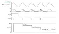
도 4는 도 3에 나타낸 디지타이저에서 포함될 수 있는 전압축적부(Voltage Accumulator)를 예시하여 도시한 도면으로, 전압축적부는 감산기(141)와, 아날로그 스위치(142) 및 샘플앤홀드부(143)로 구성되며, 이때 감산기(141)는 도 5에 나타낸 바와 같이 2단의 1차 감산기(뺄셈기)(141a)와 2차 감산기(141b)로 구성된다.FIG. 4 is a diagram illustrating a voltage accumulator included in the digitizer shown in FIG. 3. The voltage accumulator includes a
여기서, 1차 감산기(141a)는 기준전압(V1)과 센서전압(V2)을 각각 입력받아 기준전압보다 높은 전압만 절취하도록 감산한 후 출력하고, 2차 감산기(141b)는 1차 감산기(141a)의 출력값과 1차 감산기(141a)의 이전 출력값을 저장하고 있는 샘플앤홀드부(143)의 이전 출력값을 궤환입력받아 1차 감산기(141a)의 출력값에서 이전 출력값을 감산하여 아날로그 스위치(142)를 통해 샘플앤홀드부(143)로 출력한다. 이러한 과정은 제어부(160)로부터 설정된 클럭동안 지속되며, 샘플앤홀드부(143)의 출력은 설정된 클럭 이후에, 결과적으로는 Vcc로부터 시작해서 각각의 변화량만틈 감산해 가는 최종 감산 결과로 나타나게 된다.The
본 발명에 따른 전압 축적부(140)는 낮은 전압 변화를 여러 번 더함으로써 전압 변화를 크게 하고, 노이즈를 제거하기 위한 것으로, 루프센서(110)로부터의 전류는 전압으로 변환되는데, 변환된 전압은 좌표 연산에서 필요로 하는 값보다 작은 양으로 검출된다.The
따라서 적게 검출된 변화량은 이후 좌표 연산 계산에서 결과적으로 낮은 정밀도를 가져오는 요소가 되므로 이러한 작은 변화를 크게 하기 위해서 전압 축적부(140)를 이용하는 것이다.Accordingly, the lesser amount of change is an element that results in lower precision as a result of calculation of coordinate calculation thereafter, so that the
2단의 감산기 중 1차 감산기(141a)는 도 6에 나타낸 바와 같이 전압 파형 중에서 기준 전압 위 부분에 위치한 부분의 파형만을 절취한다. 즉 플러스 변화량만을 추출하며 출력은 도 6에서 Vo로 표시되었다.The
M_Sel(제어부 선택신호)의 High 영역에서 SH_CLK(샘플앤홀드 클럭)의 제1 상승 클럭에서 아날로그 스위치(142)는 Vcc(메인 전원)과 연결되며, 이러한 Vcc는 샘플엔홀드(143)에 의해 Vcc가 출력되어 유지된다.The
SH_CLK의 제2 상승 클럭 이전에 제1 상승에 의한 출력은 다시 2차 감산기(141b)의 입력으로 되돌려지며, 이 되돌려진 값과 1차 감산기(141a)의 출력은 2차 감산기(141b)의 입력으로 다시 위치하게 되며, 이 되돌려진 값과 새로운 값의 차이가 SH_CLK의 제2 상승 클럭에 의해서 샘플앤홀드부(143)의 출력으로 유지되게 된다. 즉 이전 값에서 새로운 값을 뺀 형태가 되는 것이다.The output of the first rise before the second rising clock of SH_CLK is returned to the input of the
이러한 과정이 일정 클럭동안 지속되면, 샘플앤홀드부(143)의 출력은 결과적으로 Vcc로부터 시작해서 각각의 변화량만틈 감산해 가는 최종 감산 결과로 나타나게 된다.If this process continues for a predetermined period of time, the output of the sample-and-
일종의 가산기와 마찬가지로 도 6에서와 같이 Vcc로부터 최종 Vcc-S1-S2-S3의 차이는 각각의 전압 변화량의 더하기 합이된다.6, the difference between Vcc and the final Vcc-S1-S2-S3 is the sum of the sum of the voltage variations.
이러한 전압 축적부(140)는 결국 적은 전압 변화량을 크게 만들어서 최종 좌표 계산에서 정밀도를 높이고, 각각의 전압 측정 단계(S1, S2, S3)에서의 증/감 노이즈가 서로 상쇄되도록 함으로써 최종적으로 노이즈가 제거된 출력을 얻을 수 있게 된다.This
상기한 본 발명의 바람직한 실시예는 예시의 목적을 위해 개시된 것이고, 본 발명에 대해 통상의 지식을 가진 당업자라면 본 발명의 사상과 범위 안에서 다양한 수정, 변경, 부가가 가능할 것이며, 이러한 수정, 변경 및 부가는 하기의 특허청구범위에 속하는 것으로 보아야 할 것이다.
It will be apparent to those skilled in the relevant art that various modifications, additions and substitutions are possible, without departing from the spirit and scope of the invention as defined by the appended claims. The appended claims are to be considered as falling within the scope of the following claims.
110 : 루프센서120 : 아날로그 스위칭부
130 : 차동증폭부140 : 전압축적부
150 : 아날로그 디지털 변환부160 : 제어부110: loop sensor 120: analog switching unit
130: Differential amplifier 140: Voltage accumulator
150: analog-to-digital converter 160:
Claims (5)
Translated fromKorean상기 복수의 루프센서(110)의 센싱 데이터를 선택적으로 스위칭하여 출력하는 아날로그 스위칭부(120);
상기 아날로그 스위칭부(120)의 출력을 증폭하여 출력하는 차동증폭부(130);
상기 차동증폭부(130)의 출력전압을 축적하는 전압축적부(140);
상기 전압축적부(140)에서 축적되어 출력되는 전압을 아날로그 디지털 변환하여 출력하는 아날로그 디지털 변환부(150); 및
상기 아날로그 디지털 변환부(150)에서 출력된 데이터에서 상기 루프센서(110)가 센싱한 좌표를 연산하는 제어부(160);를 포함하여 구성됨을 특징으로 하는 디지타이저.
A plurality of loop sensors (110) sensing an approach of the stylus pen;
An analog switching unit (120) for selectively switching and outputting sensing data of the plurality of loop sensors (110);
A differential amplifier 130 for amplifying and outputting the output of the analog switching unit 120;
A voltage accumulator 140 for accumulating an output voltage of the differential amplifier 130;
An analog-digital converter 150 for analog-to-digital converting the voltage accumulated in the voltage accumulator 140 and outputting the voltage; And
And a control unit (160) for calculating the coordinates sensed by the loop sensor (110) from the data output from the analog-to-digital converter (150).
상기 전압축적부(140)는 상기 차동증폭부(130)로부터 출력되는 낮은 전압 변화를 여러 번 더함으로써 전압 변화를 크게 하는 것을 특징으로 하는 디지타이저.
The method according to claim 1,
Wherein the voltage accumulator (140) increases the voltage change by adding a low voltage change output from the differential amplifier (130) several times.
상기 전압축적부(140)는 기준전압(V1)과 센서전압(V2)을 각각 입력받아 기준전압보다 높은 전압만 절취하도록 감산한 후 출력하는 1차 감산기(141a)와, 상기 1차 감산기(141a)의 출력값과 상기 1차 감산기(141a)의 이전 출력값을 궤환입력받아 상기 1차 감산기(141a)의 출력값에서 상기 이전 출력값을 감산하는 2차 감산기(141b)와, 상기 2차 감산기(141b)의 출력을 상기 제어부(160)에서 설정한 클럭만큼 저장하고 있는 샘플앤홀드부(143)로 출력하는 아날로그 스위치(142)로 구성됨을 특징으로 하는 디지타이저.
The method according to claim 1,
The voltage accumulator 140 includes a first subtracter 141a receiving a reference voltage V1 and a sensor voltage V2 and subtracting the subtracted voltage from the first subtracter 141a, A second subtractor 141b for receiving the feedback value of the output value of the first subtractor 141a and subtracting the previous output value from the output value of the first subtractor 141a, And an analog switch (142) for outputting the output to a sample and hold unit (143) that stores the output for a clock set by the control unit (160).
상기 전압 축적부(140)는 상기 설정한 클럭만큼의 저장된 전압에서 증/감 노이즈가 서로 상쇄되도록 하여 노이즈가 제거된 출력을 얻는 것을 특징으로 하는 디지타이저.
The method of claim 3,
Wherein the voltage accumulator (140) compensates for the increase / decrease noise at a stored voltage corresponding to the set clock to obtain a noise-free output.
상기 샘플앤홀드부(143)의 출력은 상기 아날로그 스위치(142)에 연결된 Vcc로부터 시작해서 상기 설정된 클럭만큼 입력되는 변화량만틈 감산해 가는 최종 감산 결과를 상기 설정한 클럭 이후에 상기 아날로그 디지털 변환부(150)로 출력하는 것을 특징으로 하는 디지타이저.
The method of claim 3,
The output of the sample and hold unit 143 is supplied to the analog-to-digital converter 142 after the final subtraction result starting from Vcc connected to the analog switch 142 and subtracting the amount of change input by the set clock, To the digitizer (150).
Applications Claiming Priority (2)
| Application Number | Priority Date | Filing Date | Title |
|---|---|---|---|
| KR20130065390 | 2013-06-07 | ||
| KR1020130065390 | 2013-06-07 |
Publications (1)
| Publication Number | Publication Date |
|---|---|
| KR20140143679Atrue KR20140143679A (en) | 2014-12-17 |
Family
ID=52674361
Family Applications (1)
| Application Number | Title | Priority Date | Filing Date |
|---|---|---|---|
| KR1020130142772ACeasedKR20140143679A (en) | 2013-06-07 | 2013-11-22 | Digitizer |
Country Status (1)
| Country | Link |
|---|---|
| KR (1) | KR20140143679A (en) |
Cited By (1)
| Publication number | Priority date | Publication date | Assignee | Title |
|---|---|---|---|---|
| KR102024378B1 (en) | 2018-12-03 | 2019-09-24 | 주식회사 코로이 | Continuous casting system |
- 2013
- 2013-11-22KRKR1020130142772Apatent/KR20140143679A/ennot_activeCeased
Cited By (1)
| Publication number | Priority date | Publication date | Assignee | Title |
|---|---|---|---|---|
| KR102024378B1 (en) | 2018-12-03 | 2019-09-24 | 주식회사 코로이 | Continuous casting system |
Similar Documents
| Publication | Publication Date | Title |
|---|---|---|
| US10310693B2 (en) | Controller for position detection | |
| JP5451181B2 (en) | Sensor device for detecting contact or proximity of an object | |
| JP5086420B2 (en) | Touch panel detection circuit | |
| US8970551B2 (en) | Method and device for position detection | |
| CN104049789B (en) | Touch-sensitive device and the method for using touch-surface circuit | |
| US8400425B2 (en) | Method and device for analyzing positions | |
| US9069427B2 (en) | High noise immunity sensing methods and apparatus for a capacitive touch device | |
| US20100328262A1 (en) | Detector and detection method for a capacitive touchpad to identify a real touch point | |
| US8674960B2 (en) | Detector circuit and detect method of a capacitive touch panel | |
| CN107092407B (en) | Inductive capacitance measuring device | |
| CN111813271B (en) | Capacitance detection circuit, touch chip and electronic equipment | |
| CN101526871A (en) | Sensing device and method of capacitive touch panel | |
| US11592936B2 (en) | Capacitive touch device with high sensitivity and low power consumption | |
| US20110050633A1 (en) | Detector circuit and detect method of a capacitive touch panel | |
| KR20140143679A (en) | Digitizer | |
| KR101531652B1 (en) | Digitizer and Method for filtering noise thereof | |
| WO2015166568A1 (en) | Input device, input method, and program | |
| CN102004588B (en) | Capacitive touch panel detection circuit and method | |
| CN102819369B (en) | Method for Improving Accuracy of Touch Coordinate Calculation in Capacitive Multi-touch System | |
| CN102981663A (en) | Electret input device and operation method thereof | |
| EP2511803A1 (en) | Method and device for analyzing position |
Legal Events
| Date | Code | Title | Description |
|---|---|---|---|
| A201 | Request for examination | ||
| PA0109 | Patent application | Patent event code:PA01091R01D Comment text:Patent Application Patent event date:20131122 | |
| PA0201 | Request for examination | ||
| PG1501 | Laying open of application | ||
| E902 | Notification of reason for refusal | ||
| PE0902 | Notice of grounds for rejection | Comment text:Notification of reason for refusal Patent event date:20150226 Patent event code:PE09021S01D | |
| E601 | Decision to refuse application | ||
| PE0601 | Decision on rejection of patent | Patent event date:20150605 Comment text:Decision to Refuse Application Patent event code:PE06012S01D Patent event date:20150226 Comment text:Notification of reason for refusal Patent event code:PE06011S01I |