KR20140143634A - Organic light emitting diode display - Google Patents
Organic light emitting diode displayDownload PDFInfo
- Publication number
- KR20140143634A KR20140143634AKR1020130065467AKR20130065467AKR20140143634AKR 20140143634 AKR20140143634 AKR 20140143634AKR 1020130065467 AKR1020130065467 AKR 1020130065467AKR 20130065467 AKR20130065467 AKR 20130065467AKR 20140143634 AKR20140143634 AKR 20140143634A
- Authority
- KR
- South Korea
- Prior art keywords
- buffer member
- light emitting
- organic light
- peripheral
- display panel
- Prior art date
- Legal status (The legal status is an assumption and is not a legal conclusion. Google has not performed a legal analysis and makes no representation as to the accuracy of the status listed.)
- Granted
Links
Images


Classifications
- H—ELECTRICITY
- H04—ELECTRIC COMMUNICATION TECHNIQUE
- H04M—TELEPHONIC COMMUNICATION
- H04M1/00—Substation equipment, e.g. for use by subscribers
- H04M1/02—Constructional features of telephone sets
- H04M1/18—Telephone sets specially adapted for use in ships, mines, or other places exposed to adverse environment
- H04M1/185—Improving the shock resistance of the housing, e.g. by increasing the rigidity
- G—PHYSICS
- G06—COMPUTING OR CALCULATING; COUNTING
- G06F—ELECTRIC DIGITAL DATA PROCESSING
- G06F1/00—Details not covered by groups G06F3/00 - G06F13/00 and G06F21/00
- G06F1/16—Constructional details or arrangements
- G06F1/1613—Constructional details or arrangements for portable computers
- G06F1/1633—Constructional details or arrangements of portable computers not specific to the type of enclosures covered by groups G06F1/1615 - G06F1/1626
- G06F1/1637—Details related to the display arrangement, including those related to the mounting of the display in the housing
- G—PHYSICS
- G09—EDUCATION; CRYPTOGRAPHY; DISPLAY; ADVERTISING; SEALS
- G09F—DISPLAYING; ADVERTISING; SIGNS; LABELS OR NAME-PLATES; SEALS
- G09F9/00—Indicating arrangements for variable information in which the information is built-up on a support by selection or combination of individual elements
- G09F9/30—Indicating arrangements for variable information in which the information is built-up on a support by selection or combination of individual elements in which the desired character or characters are formed by combining individual elements
- G09F9/301—Indicating arrangements for variable information in which the information is built-up on a support by selection or combination of individual elements in which the desired character or characters are formed by combining individual elements flexible foldable or roll-able electronic displays, e.g. thin LCD, OLED
- G—PHYSICS
- G09—EDUCATION; CRYPTOGRAPHY; DISPLAY; ADVERTISING; SEALS
- G09G—ARRANGEMENTS OR CIRCUITS FOR CONTROL OF INDICATING DEVICES USING STATIC MEANS TO PRESENT VARIABLE INFORMATION
- G09G3/00—Control arrangements or circuits, of interest only in connection with visual indicators other than cathode-ray tubes
- G09G3/20—Control arrangements or circuits, of interest only in connection with visual indicators other than cathode-ray tubes for presentation of an assembly of a number of characters, e.g. a page, by composing the assembly by combination of individual elements arranged in a matrix no fixed position being assigned to or needed to be assigned to the individual characters or partial characters
- G09G3/22—Control arrangements or circuits, of interest only in connection with visual indicators other than cathode-ray tubes for presentation of an assembly of a number of characters, e.g. a page, by composing the assembly by combination of individual elements arranged in a matrix no fixed position being assigned to or needed to be assigned to the individual characters or partial characters using controlled light sources
- G09G3/30—Control arrangements or circuits, of interest only in connection with visual indicators other than cathode-ray tubes for presentation of an assembly of a number of characters, e.g. a page, by composing the assembly by combination of individual elements arranged in a matrix no fixed position being assigned to or needed to be assigned to the individual characters or partial characters using controlled light sources using electroluminescent panels
- G09G3/32—Control arrangements or circuits, of interest only in connection with visual indicators other than cathode-ray tubes for presentation of an assembly of a number of characters, e.g. a page, by composing the assembly by combination of individual elements arranged in a matrix no fixed position being assigned to or needed to be assigned to the individual characters or partial characters using controlled light sources using electroluminescent panels semiconductive, e.g. using light-emitting diodes [LED]
- G09G3/3208—Control arrangements or circuits, of interest only in connection with visual indicators other than cathode-ray tubes for presentation of an assembly of a number of characters, e.g. a page, by composing the assembly by combination of individual elements arranged in a matrix no fixed position being assigned to or needed to be assigned to the individual characters or partial characters using controlled light sources using electroluminescent panels semiconductive, e.g. using light-emitting diodes [LED] organic, e.g. using organic light-emitting diodes [OLED]
- H—ELECTRICITY
- H04—ELECTRIC COMMUNICATION TECHNIQUE
- H04M—TELEPHONIC COMMUNICATION
- H04M1/00—Substation equipment, e.g. for use by subscribers
- H04M1/02—Constructional features of telephone sets
- H04M1/0202—Portable telephone sets, e.g. cordless phones, mobile phones or bar type handsets
- H04M1/026—Details of the structure or mounting of specific components
- H04M1/0266—Details of the structure or mounting of specific components for a display module assembly
- H—ELECTRICITY
- H05—ELECTRIC TECHNIQUES NOT OTHERWISE PROVIDED FOR
- H05B—ELECTRIC HEATING; ELECTRIC LIGHT SOURCES NOT OTHERWISE PROVIDED FOR; CIRCUIT ARRANGEMENTS FOR ELECTRIC LIGHT SOURCES, IN GENERAL
- H05B33/00—Electroluminescent light sources
- H05B33/02—Details
- H05B33/04—Sealing arrangements, e.g. against humidity
- H—ELECTRICITY
- H10—SEMICONDUCTOR DEVICES; ELECTRIC SOLID-STATE DEVICES NOT OTHERWISE PROVIDED FOR
- H10K—ORGANIC ELECTRIC SOLID-STATE DEVICES
- H10K50/00—Organic light-emitting devices
- H10K50/80—Constructional details
- H10K50/84—Passivation; Containers; Encapsulations
- H10K50/841—Self-supporting sealing arrangements
- H—ELECTRICITY
- H10—SEMICONDUCTOR DEVICES; ELECTRIC SOLID-STATE DEVICES NOT OTHERWISE PROVIDED FOR
- H10K—ORGANIC ELECTRIC SOLID-STATE DEVICES
- H10K59/00—Integrated devices, or assemblies of multiple devices, comprising at least one organic light-emitting element covered by group H10K50/00
- H10K59/10—OLED displays
- H10K59/12—Active-matrix OLED [AMOLED] displays
- H10K59/126—Shielding, e.g. light-blocking means over the TFTs
- G—PHYSICS
- G09—EDUCATION; CRYPTOGRAPHY; DISPLAY; ADVERTISING; SEALS
- G09G—ARRANGEMENTS OR CIRCUITS FOR CONTROL OF INDICATING DEVICES USING STATIC MEANS TO PRESENT VARIABLE INFORMATION
- G09G3/00—Control arrangements or circuits, of interest only in connection with visual indicators other than cathode-ray tubes
- G09G3/20—Control arrangements or circuits, of interest only in connection with visual indicators other than cathode-ray tubes for presentation of an assembly of a number of characters, e.g. a page, by composing the assembly by combination of individual elements arranged in a matrix no fixed position being assigned to or needed to be assigned to the individual characters or partial characters
- G09G3/22—Control arrangements or circuits, of interest only in connection with visual indicators other than cathode-ray tubes for presentation of an assembly of a number of characters, e.g. a page, by composing the assembly by combination of individual elements arranged in a matrix no fixed position being assigned to or needed to be assigned to the individual characters or partial characters using controlled light sources
- G09G3/30—Control arrangements or circuits, of interest only in connection with visual indicators other than cathode-ray tubes for presentation of an assembly of a number of characters, e.g. a page, by composing the assembly by combination of individual elements arranged in a matrix no fixed position being assigned to or needed to be assigned to the individual characters or partial characters using controlled light sources using electroluminescent panels
- H—ELECTRICITY
- H10—SEMICONDUCTOR DEVICES; ELECTRIC SOLID-STATE DEVICES NOT OTHERWISE PROVIDED FOR
- H10K—ORGANIC ELECTRIC SOLID-STATE DEVICES
- H10K59/00—Integrated devices, or assemblies of multiple devices, comprising at least one organic light-emitting element covered by group H10K50/00
- H10K59/80—Constructional details
- H10K59/87—Passivation; Containers; Encapsulations
- H10K59/871—Self-supporting sealing arrangements
Landscapes
- Engineering & Computer Science (AREA)
- Physics & Mathematics (AREA)
- Theoretical Computer Science (AREA)
- Computer Hardware Design (AREA)
- General Physics & Mathematics (AREA)
- Signal Processing (AREA)
- Optics & Photonics (AREA)
- Human Computer Interaction (AREA)
- General Engineering & Computer Science (AREA)
- Microelectronics & Electronic Packaging (AREA)
- Electroluminescent Light Sources (AREA)
- Devices For Indicating Variable Information By Combining Individual Elements (AREA)
Abstract
Translated fromKoreanDescription
Translated fromKorean본 발명은 유기 발광 표시 장치에 관한 것으로, 보다 상세하게는 완충부재를 포함하는 유기 발광 표시 장치에 관한 것이다.BACKGROUND OF THE
유기 발광 표시 장치(organic light emitting diode display)는 정공 주입 전극과 전자 주입 전극 그리고 이들 사이에 형성되어 있는 유기 발광층을 포함하며, 애노드에서 주입되는 정공과 캐소드에서 주입되는 전자가 유기 발광층에서 재결합하여 소멸하면서 빛을 내는 자발광형 표시 장치이다.An organic light emitting diode (OLED) display includes a hole injection electrode, an electron injection electrode, and an organic light emitting layer formed therebetween. The holes injected from the anode and the electrons injected from the cathode recombine in the organic light emitting layer, Emitting display device that emits light while emitting light.
유기 발광 표시 장치는 낮은 소비 전력, 높은 휘도 및 높은 반응 속도 등의 고품위 특성을 나타내므로 휴대용 전자 기기의 차세대 표시 장치로 주목받고 있다. 그러나, 유기 발광 표시 장치는 외부의 충격에 의하여 패널에 찍힘 또는 눌림과 같은 불량이 발생하므로, 이를 방지하기 위한 완충부재가 요구된다.BACKGROUND ART [0002] Organic light emitting display devices are attracting attention as next-generation display devices for portable electronic devices because they exhibit high-quality characteristics such as low power consumption, high luminance, and high response speed. However, an organic light emitting display device is required to have a buffering member for preventing it from being stuck on the panel due to an external impact or causing defects such as pressing.
본 발명의 일 측면에 따르면, 패널의 외관상에 발생하는 불량을 방지할 수 있는 완충부재를 포함하는 유기 발광 표시 장치를 제공하고자 한다.According to an aspect of the present invention, there is provided an organic light emitting display device including a buffer member capable of preventing defects occurring on the outer surface of a panel.
상기와 같은 목적을 달성하기 위하여, 표시 패널; 상기 표시 패널이 실장되는 베젤; 및 상기 표시 패널의 하면과 상기 베젤 사이에 배치되는 완충부재;를 포함하며, 상기 완충부재는 주변 완충부재 및 상기 주변 완충부재에 의해 에워싸이며 계단 형상의 구조를 갖는 중심 완충부재;를 포함하는 유기 발광 표시 장치를 제공한다.According to an aspect of the present invention, A bezel on which the display panel is mounted; And a cushioning member disposed between the lower surface of the display panel and the bezel, wherein the cushioning member is surrounded by the peripheral cushioning member and the peripheral cushioning member and has a stepped structure An organic light emitting display device is provided.
본 발명의 다른 특징에 의하면, 상기 중심 완충부재는 상기 표시 패널의 하면에서 상기 베젤 쪽으로 갈수록 폭이 더 좁아질 수 있다.According to another aspect of the present invention, the width of the center buffer member may become narrower toward the bezel from the lower surface of the display panel.
본 발명의 또 다른 특징에 의하면, 상기 주변 완충부재와 상기 중심 완충부재는 서로 이격되어 배치될 수 있다.According to another aspect of the present invention, the peripheral buffer member and the center buffer member may be spaced apart from each other.
본 발명의 또 다른 특징에 의하면, 상기 중심 완충부재는, 상기 표시 패널의 하면에 배치되는 제1 중심 완충부재; 및 상기 제1 중심 완충부재의 하면 상에 배치되는 제2 중심 완충부재;를 포함하며, 상기 제2 중심 완충부재의 폭은 상기 제1 중심 완충부재의 폭보다 더 좁을 수 있다.According to another aspect of the present invention, the center cushioning member includes: a first center cushioning member disposed on a lower surface of the display panel; And a second center cushioning member disposed on a lower surface of the first center cushioning member, wherein a width of the second center cushioning member may be narrower than a width of the first center cushioning member.
본 발명의 또 다른 특징에 의하면, 상기 제2 중심 완충부재의 하면 상에 배치되는 제3 중심 완충부재;를 더 포함하며, 상기 제3 중심 완충부재의 폭은 상기 제2 중심 완충부재의 폭보다 더 좁을 수 있다.According to another aspect of the present invention, there is further provided a third center cushioning member disposed on the lower surface of the second center cushioning member, wherein the width of the third center cushioning member is larger than the width of the second center cushioning member Can be narrower.
본 발명의 또 다른 특징에 의하면, 상기 주변 완충부재의 일측면과 상기 중심 완충부재의 일측면은 서로 접할 수 있다.According to another aspect of the present invention, one side of the peripheral buffer member and one side of the center buffer member may be in contact with each other.
본 발명의 또 다른 특징에 의하면, 상기 완충부재는, 상기 기판과 상기 주변 완충부재 사이, 및 상기 기판과 상기 중심 완충부재 사이에 배치되는 제1 점착층;을 포함할 수 있다.According to still another aspect of the present invention, the buffer member may include a first adhesive layer disposed between the substrate and the peripheral buffer member, and between the substrate and the center buffer member.
본 발명의 또 다른 특징에 의하면, 상기 완충부재는, 상기 주변 완충부재의 하면에 배치되는 제2 점착층;을 더 포함할 수 있다.According to another aspect of the present invention, the buffer member may further include a second adhesive layer disposed on a lower surface of the peripheral buffer member.
본 발명의 또 다른 특징에 의하면, 상기 제2 점착층은, 도전성 점착층 일 수 있다.According to another aspect of the present invention, the second adhesive layer may be a conductive adhesive layer.
본 발명의 또 다른 특징에 의하면, 상기 제2 점착층의 하면 및 상기 중심 완충부재의 하면은, 상기 베젤과 접할 수 있다.According to another aspect of the present invention, the bottom surface of the second adhesive layer and the bottom surface of the center cushioning member can be in contact with the bezel.
본 발명의 또 다른 특징에 의하면, 상기 주변 완충부재는, 스펀지 또는 우레탄 일 수 있다.According to another aspect of the present invention, the peripheral buffer member may be a sponge or a urethane.
본 발명의 또 다른 특징에 의하면, 상기 중심 완충부재는, 실리콘, 폴리에틸렌(PET) 필름, 또는 러버(Rubber) 일 수 있다.According to another aspect of the present invention, the center buffer member may be a silicone, a polyethylene (PET) film, or a rubber.
본 발명의 또 다른 특징에 의하면, 상기 표시 패널은, 기판; 상기 기판 상에 형성되며 박막 트랜지스터를 포함하는 구동 회로부; 상기 기판 상에 형성되며 상기 구동 회로부와 연결된 유기 발광 소자; 및 상기 기판 상에 형성되며 상기 유기 발광 소자 및 상기 구동 회로부를 덮는 봉지층;을 포함할 수 있다.According to another aspect of the present invention, the display panel includes a substrate; A driving circuit formed on the substrate and including a thin film transistor; An organic light emitting diode formed on the substrate and connected to the driving circuit; And a sealing layer formed on the substrate and covering the organic light emitting device and the driving circuit.
본 발명의 또 다른 특징에 의하면, 상기 베젤은, 상기 표시 패널이 실장되는 바닥부; 및 상기 바닥부의 가장자리로부터 연장되어 상기 표시 패널의 측면과 마주하는 측벽;을 포함할 수 있다.According to another aspect of the present invention, the bezel includes: a bottom portion on which the display panel is mounted; And side walls extending from an edge of the bottom portion and facing a side surface of the display panel.
본 발명의 또 다른 특징에 의하면, 상기 표시 패널의 상부 및 상기 베젤의 상부를 덮도록 형성된 투과부;를 더 포함할 수 있다.According to another aspect of the present invention, the display device may further include a transmissive portion formed to cover the upper portion of the display panel and the upper portion of the bezel.
또한 전술한 목적을 달성하기 위하여, 표시 패널; 상기 표시 패널이 실장되는 베젤; 및 상기 표시 패널의 하면과 상기 베젤 사이에 배치되는 완충부재;를 포함하며, 상기 완충부재는 주변 완충부재 및 상기 주변 완충부재에 의해 에워싸이며 하단부가 볼록한 곡면 형상을 갖는 중심 완충부재;를 포함하는 유기 발광 표시 장치를 제공한다.In addition, in order to achieve the above object, A bezel on which the display panel is mounted; And a cushioning member disposed between the lower surface of the display panel and the bezel, wherein the cushioning member is surrounded by the peripheral cushioning member and the peripheral cushioning member, and the curved surface shape of which the lower end is convex And an organic light emitting display device.
본 발명의 또 다른 특징에 의하면, 상기 주변 완충부재와 상기 중심 완충부재는 서로 이격되어 배치될 수 있다.According to another aspect of the present invention, the peripheral buffer member and the center buffer member may be spaced apart from each other.
본 발명의 또 다른 특징에 의하면, 상기 완충부재는, 상기 기판과 상기 주변 완충부재 사이, 및 상기 기판과 상기 중심 완충부재 사이에 배치되는 제1 점착층;을 포함할 수 있다.According to still another aspect of the present invention, the buffer member may include a first adhesive layer disposed between the substrate and the peripheral buffer member, and between the substrate and the center buffer member.
본 발명의 또 다른 특징에 의하면, 상기 완충부재는, 상기 주변 완충부재의 하면에 배치되는 제2 점착층;을 더 포함할 수 있다.According to another aspect of the present invention, the buffer member may further include a second adhesive layer disposed on a lower surface of the peripheral buffer member.
본 발명의 또 다른 특징에 의하면, 상기 제2 점착층의 하면 및 상기 중심 완충부재의 하면은, 상기 베젤과 접할 수 있다.According to another aspect of the present invention, the bottom surface of the second adhesive layer and the bottom surface of the center cushioning member can be in contact with the bezel.
본 발명의 또 다른 특징에 의하면, 상기 중심 완충부재의 최하단까지의 두께는, 상기 주변 완충부재의 두께 및 상기 제2 점착층의 두께의 합보다 더 클 수 있다.According to another aspect of the present invention, the thickness of the center buffer member to the lowermost end may be greater than the sum of the thickness of the peripheral buffer member and the thickness of the second adhesive layer.
본 발명의 또 다른 특징에 의하면, 상기 주변 완충부재는, 스펀지 또는 우레탄 일 수 있다.According to another aspect of the present invention, the peripheral buffer member may be a sponge or a urethane.
본 발명의 또 다른 특징에 의하면, 상기 중심 완충부재는, 실리콘, 폴리에틸렌(PET) 필름, 또는 러버(Rubber) 일 수 있다.According to another aspect of the present invention, the center buffer member may be a silicone, a polyethylene (PET) film, or a rubber.
본 발명의 일 측면에 따르면, 내구성이 향상된 유기 발광 표시 장치를 제공할 수 있다.According to an aspect of the present invention, an organic light emitting display device having improved durability can be provided.
도 1은 본 발명의 일 실시예에 따른 유기 발광 표시 장치(1)를 개략적으로 도시한 단면도이다.
도 2는 도 1의 "A" 부분을 확대하여 나타낸 단면도이다.
도 3 내지 도 7은 다른 실시예에 따른 도 1의 "A" 부분의 구조를 개략적으로 도시한 단면도들이다. 도 8은 도 1에 도시된 표시 패널의 일 화소의 화소 회로를 나타내는 회로도이다.
도 9는 표시 패널의 화소 구조를 나타내는 배치도이다.
도 10는 도 9의 Ⅵ-Ⅵ선에 따른 표시 패널의 단면을 나타내는 단면도이다.1 is a cross-sectional view schematically showing an organic light emitting
2 is an enlarged cross-sectional view of the portion "A" in Fig.
Figs. 3 to 7 are cross-sectional views schematically showing the structure of the "A" portion of Fig. 1 according to another embodiment. 8 is a circuit diagram showing a pixel circuit of one pixel of the display panel shown in Fig.
9 is a layout diagram showing the pixel structure of the display panel.
10 is a cross-sectional view showing a section of the display panel taken along the line VI-VI in Fig.
본 발명은 다양한 변환을 가할 수 있고 여러 가지 실시 예를 가질 수 있는 바, 특정 실시 예들을 도면에 예시하고 상세한 설명에 상세하게 설명하고자 한다. 그러나, 이는 본 발명을 특정한 실시 형태에 대해 한정하려는 것이 아니며, 본 발명의 사상 및 기술 범위에 포함되는 모든 변환, 균등물 내지 대체물을 포함하는 것으로 이해되어야 한다. 본 발명을 설명함에 있어서 관련된 공지 기술에 대한 구체적인 설명이 본 발명의 요지를 흐릴 수 있다고 판단되는 경우 그 상세한 설명을 생략한다.BRIEF DESCRIPTION OF THE DRAWINGS The present invention is capable of various modifications and various embodiments, and specific embodiments are illustrated in the drawings and described in detail in the detailed description. It is to be understood, however, that the invention is not to be limited to the specific embodiments, but includes all modifications, equivalents, and alternatives falling within the spirit and scope of the invention. DETAILED DESCRIPTION OF THE PREFERRED EMBODIMENTS Hereinafter, the present invention will be described in detail with reference to the accompanying drawings.
제1, 제2 등의 용어는 다양한 구성요소들을 설명하는데 사용될 수 있지만, 구성요소들은 용어들에 의해 한정되어서는 안 된다. 용어들은 하나의 구성요소를 다른 구성요소로부터 구별하는 목적으로만 사용된다.The terms first, second, etc. may be used to describe various elements, but the elements should not be limited by terms. Terms are used only for the purpose of distinguishing one component from another.
본 출원에서 사용한 용어는 단지 특정한 실시 예를 설명하기 위해 사용된 것으로, 본 발명을 한정하려는 의도가 아니다. 단수의 표현은 문맥상 명백하게 다르게 뜻하지 않는 한, 복수의 표현을 포함한다. 본 출원에서, "포함하다" 또는 "가지다" 등의 용어는 명세서상에 기재된 특징, 숫자, 단계, 동작, 구성요소, 부품 또는 이들을 조합한 것이 존재함을 지정하려는 것이지, 하나 또는 그 이상의 다른 특징들이나 숫자, 단계, 동작, 구성요소, 부품 또는 이들을 조합한 것들의 존재 또는 부가 가능성을 미리 배제하지 않는 것으로 이해되어야 한다.The terminology used in this application is used only to describe a specific embodiment and is not intended to limit the invention. The singular expressions include plural expressions unless the context clearly dictates otherwise. In the present application, the terms "comprises" or "having" and the like are used to specify that there is a feature, a number, a step, an operation, an element, a component or a combination thereof described in the specification, But do not preclude the presence or addition of one or more other features, integers, steps, operations, elements, components, or combinations thereof.
또한, 도면에서 나타난 각 구성의 크기 및 두께는 설명의 편의를 위해 임의로 나타내었으므로, 본 발명이 반드시 도시된 바에 한정되지 않는다.In addition, since the sizes and thicknesses of the respective components shown in the drawings are arbitrarily shown for convenience of explanation, the present invention is not necessarily limited to those shown in the drawings.
도면에서 여러 층 및 영역을 명확하게 표현하기 위하여 두께를 확대하여 나타내었다. 그리고 도면에서, 설명의 편의를 위해, 일부 층 및 영역의 두께를 과장되게 나타내었다. 층, 막, 영역, 판 등의 부분이 다른 부분 “위에” 또는 “상에” 있다고 할 때, 이는 다른 부분 “바로 위에” 있는 경우뿐 아니라 그 중간에 또 다른 부분이 있는 경우도 포함한다.In the drawings, the thickness is enlarged to clearly represent the layers and regions. In the drawings, for the convenience of explanation, the thicknesses of some layers and regions are exaggerated. Whenever a portion such as a layer, film, region, plate, or the like is referred to as being "on" or "on" another portion, it includes not only the case where it is "directly on" another portion but also the case where there is another portion in between.
이하, 첨부된 도면을 참조로 본 발명의 바람직한 실시예들에 대하여 보다 상세히 설명한다.Hereinafter, preferred embodiments of the present invention will be described in detail with reference to the accompanying drawings.
도 1은 본 발명의 일 실시예에 따른 유기 발광 표시 장치(1)를 개략적으로 도시한 단면도이다.1 is a cross-sectional view schematically showing an organic light emitting
본 발명의 실시예에 따른 유기 발광 표시 장치(1)는 기판(110)의 하면에 주변 완충부재(220) 및 상기 주변 완충부재(220)에 의하여 에워싸이며 계단 형상의 구조를 갖는 중심 완충부재(230)를 포함한다. 따라서, 외부 충격에 의해서 유기 발광 표시 장치(1)에 찍힘 또는 눌림 불량이 발생하는 것을 방지하여 유기 발광 표시 장치(1)의 신뢰도를 높일 수 있다.The organic light emitting
도 1을 참조하면, 본 발명의 일 실시예에 따른 유기 발광 표시 장치(1)는 표시 패널(100), 표시 패널(100)이 실장되는 베젤(300), 투과부(400) 및 완충부재(200)를 포함한다.1, an
표시 패널(100)은 기판(110), 구동 회로부(130), 유기 발광 소자(140), 및 봉지층(150)을 포함한다.The
기판(110)은 폴리에틸렌에테르프탈레이트, 폴리에틸렌나프탈레이트, 폴리카보네이트, 폴리아릴레이트, 폴리에테르이미드, 폴리에테르술폰 및 폴리이미드 등과 같은 플라스틱으로 구성될 수 있다. 또한, 기판(110)은 얇은 유리 또는 스테인리스 강 등으로 이루어진 금속성 기판으로 형성될 수도 있다.The
구동 회로부(130)는 박막 트랜지스터(10, 20)(도 9 및 도 10 참조)를 포함하며, 유기 발광 소자(140)를 구동한다. 유기 발광 소자(140)는 구동 회로부(130)와 연결되어 구동 회로부(130)로부터 전달받은 구동 신호에 따라 빛을 방출하여 화상을 표시한다.The driving
구동 회로부(130) 및 유기 발광 소자(140)의 구체적인 구조는 도 9 및 도 10에 도시되어 있으나, 본 발명의 일 실시예가 도 9 및 도 10에 도시된 구조에 한정되는 것은 아니다. 구동 회로부(130) 및 유기 발광 소자(140)는 해당 기술 분야의 전문가가 용이하게 변형 실시할 수 있는 범위 내에서 다양한 구조로 형성될 수 있다.The specific structure of the driving
봉지층(150)은 구동 회로부(130) 및 유기 발광 소자(140)를 덮도록 형성되며, 구체적으로 도시하지는 않았으나 다층 구조로 형성될 수 있다. 봉지층(150)은 복수의 무기막들로 형성되거나, 무기막 및 유기막이 서로 교번하여 형성될 수도 있다. 본 발명의 일 실시예에서, 봉지층(150)은 해당 기술 분야에 종사하는 자에게 공지된 다양한 종류의 무기막들 및 유기막들을 사용하여 형성할 수 있다.The
또한, 표시 패널(100)은 가요성 기판(110)과 구동 회로부(130) 사이에 배치된 베리어막(120)을 더 포함할 수 있다.The
베리어막(120)은 다양한 무기막들 및 유기막들 중에서 선택된 적어도 하나 이상의 막으로 형성될 수 있다. 유기 발광 소자(140)에 침투한 수분은 유기 발광 소자(140)의 수명을 단축시킨다. 따라서, 베리어막(120)은 수분과 같이 불필요한 성분이 가요성 기판(110)을 투과하여 유기 발광 소자(140)에 침투하는 것을 방지한다.The
베젤(300)은 표시 패널(100)이 실장되는 바닥부(310) 및 바닥부(310)의 가장자리로부터 표시 패널(100)을 향해 연장되어 표시 패널(100)의 측면과 마주하는 측벽(320)을 포함한다. 베젤(300)의 구조는 도시한 예에 한정되지 않으며, 다양하게 변형 가능하다.The
베젤(300)은 강성이 높은 재료, 예를 들어 스테인리스 강, 냉간압연 강, 알루미늄, 알루미늄 합금, 니켈 합금 등의 금속 소재로 형성될 수 있다. 또는, 베젤(300)은 합성수지 소재로 형성될 수 있으며, 예를 들어 폴리카보네이트와 같은 폴리머 계통의 엔지니어링 플라스틱으로 형성될 수 있다.The
투과부(400)는 표시 패널(100)의 표시 영역 상에 배치되며, 표시 패널(100)에서 방출되는 빛을 투과시킨다. 투과부(400)는 유리 또는 투명한 합성수지 필름으로 형성될 수 있다. 합성수지 필름은 예를 들어, 폴리에틸렌(PET) 필름, 폴리프로필렌(PP) 필름, 폴리아미드(PA) 필름, 폴리아세탈(POM) 필름, 폴리메틸메타크릴레이트(PMMA) 필름, 폴리부틸렌테레프탈레이트(PBT) 필름, 폴리카보네이트(PC) 필름, 셀룰로오스 필름 또는 방습 셀로판 일 수 있다. 투과부(400)는 합성수지 필름으로 형성되어 투명도가 높고, 내마모성과 내충격성 및 방습특성을 가지며, 질기고 튼튼한 특성을 갖는다.The
투과부(400)는 표시 패널(100)의 표시 영역 상에 배치되므로, 상기 표시 영역의 형상에 대응되는 형상을 가질 수 있다.Since the
완충부재(200)는 주변 완충부재(220), 중심 완충부재(230), 및 제1 점착층(210)을 포함한다.The
주변 및 중심 완충부재(220, 230)는 완충 기능을 하며, 중심 완충부재(230)는 주변 완충부재(220)에 의하여 에워싸이며 계단 형상의 구조를 갖는다. 제1 점착층(210)은 기판(110)과 상기 주변 및 중심 완충부재(220, 230) 사이에 위치하여, 주변 및 중심 완충부재(220, 230)를 기판(110)의 하면에 위치하도록 한다.The peripheral and
주변 완충부재(220)는 고무액을 발포 성형한 스펀지 또는 고무액을 합성수지 형태로 제조한 우레탄으로 형성될 수 있다. 그러나, 본 발명의 실시예는 이에 한정되지 않는다.The
중심 완충부재(230)는 주변 완충부재(220)로부터 소정의 거리만큼 이격되어 형성되며, 제1 점착층(210) 상에 순차로 적층된 계단 형상의 제1 중심 완충부재(230a) 및 제2 중심 완충부재(230b)를 포함한다.The
제1 중심 완충부재(230a)는 제2 중심 완충부재(230b) 보다 더 넓은 폭을 가지며, 제1 및 제2 중심 완충부재(230a, 230b)는 동일한 물질로 형성될 수 있다.The first
중심 완충부재(230)는 탄성 변형이 가능한 실리콘, 폴리에틸렌(PET) 필름, 또는 러버(Rubber) 재질로 형성될 수 있다. 그러나, 본 발명의 실시예는 이에 한정되지 않는다.The
완충부재(200)는 주변 완충부재(230)의 하면에 배치되는 제2 점착층(240)을 더 포함할 수 있다.The
제2 점착층(240)은 표시 패널(100)과 베젤(300)의 바닥부(310)를 서로 결합시킨다. 또한, 제2 점착층(240)은 도전성 점착층으로서, 정전기에 의하여 유기 발광 표시 장치(1)가 망가지는 것을 방지할 수 있다.The second
본 발명의 실시예에 따르면, 완충부재(200)는 계단 형태의 복수의 층으로 형성된 중심 완충부재(230) 및 주변 완충부재(220)를 포함함으로써, 중심 완충부재(230)와 주변 완충부재(220)의 경계부에서 압력 차이를 줄일 수 있고, 이를 통하여 외부에서 유기 발광 표시 장치(1)에 가해지는 충격에 의한 찍힘 또는 눌림 불량을 방지할 수 있다.
According to the embodiment of the present invention, the
도 2는 도 1의 "A" 부분을 확대하여 나타낸 단면도이다.2 is an enlarged cross-sectional view of the portion "A" in Fig.
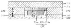
도 2를 참조하면, 주변 완충부재(220)의 두께(d1)와 제2 점착층(240)의 두께(d2)의 합(d1+d2)은, 중심 완충부재(230)의 두께(d3+d4)와 서로 동일하다. 따라서, 제2 점착층(240)의 하면은 베젤(300)과 접촉하면서 베젤과 결합되며, 중심 완충부재(230)의 제2 중심 완충부재(230b) 또한 베젤(300)과 접촉할 수 있다.
2, the sum (d1 + d2) of the thickness d1 of the
도 3 내지 도 7은 다른 실시예에 따른 도 1의 "A" 부분의 구조를 개략적으로 도시한 단면도들이다. 여기서, 앞서 도시된 도면에서와 동일한 참조부호는 동일한 기능을 하는 동일한 부재를 가리키므로, 이에 대한 설명은 생략한다.Figs. 3 to 7 are cross-sectional views schematically showing the structure of the "A" portion of Fig. 1 according to another embodiment. Here, the same reference numerals as those shown in the drawings denote the same members having the same function, and a description thereof will be omitted.
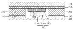
도 3을 참조하면, 완충부재(240)는 주변 완충부재(220) 및 상기 주변 완충부재(220)에 의하여 에워싸이며 계단 형상의 구조를 갖는 중심 완충부재(230)를 포함한다. 상기 주변 완충부재(220)와 중심 완충부재(230)는 소정의 거리만큼 서로 이격되어 형성된다.Referring to FIG. 3, the
중심 완충부재(220)는 도 2와 달리, 세 개의 층을 이루는 제1 내지 제3 중심 완충부재(220a, 220b, 220c)를 포함한다. 제1 내지 제3 중심 완충부재(220a, 220b, 220c)는 폭이 점점 좁아지는 계단 형상의 구조를 가진다.The
또한, 주변 완충부재(220)의 두께(d1)와 제2 점착층(240)의 두께(d2)의 합(d1+d2)은, 중심 완충부재(230)의 두께(d3+d4+d5)와 서로 동일하다. 따라서, 제2 점착층(240)의 하면은 베젤(300)과 접촉하면서 베젤과 결합되며, 중심 완충부재(230)의 제3 중심 완충부재(230c) 또한 베젤(300)과 접촉할 수 있다.
The sum d1 + d2 of the thickness d1 of the
도 4을 참조하면, 완충부재(240)는 주변 완충부재(220) 및 상기 주변 완충부재(220)에 의하여 에워싸이며 계단 형상의 구조를 갖는 중심 완충부재(230)를 포함한다. 중심 완충부재(230)는 폭이 점점 좁아지는 제1 중심 완충부재(230a) 및 제2 중심 완충부재(230b)를 포함한다.Referring to FIG. 4, the
도 2와 달리, 주변 완충부재(220)의 일 측면과 제1 중심 완충부재(230a)의 일 측면은 서로 접하도록 형성된다.
2, one side of the
도 5를 참조하면, 완충부재(240)는 주변 완충부재(220) 및 상기 주변 완충부재(220)에 의하여 에워싸이며 계단 형상의 구조를 갖는 중심 완충부재(230)를 포함한다. 중심 완충부재(230)는 폭이 점점 좁아지는 제1 중심 완충부재(230a) 내지 제3 중심 완충부재(230c)를 포함한다.Referring to FIG. 5, the
도 3과 달리, 주변 완충부재(220)의 일 측면과 제1 중심 완충부재(230a)의 일 측면은 서로 접하도록 형성된다.
3, one side of the
도 6을 참조하면, 완충부재(240)는 주변 완충부재(220) 및 상기 주변 완충부재(220)에 의하여 에워싸이며 하단부가 볼록한 곡면 형상을 갖는 중심 완충부재(230d)를 포함한다. 상기 주변 완충부재(220)와 중심 완충부재(230d)는 소정의 거리만큼 서로 이격되어 형성된다. 중심 완충부재(230d)는 하단부가 볼록한 곡면 형상을 갖도록, 사출 성형을 통하여 형성될 수 있다.Referring to FIG. 6, the
주변 완충부재(220)의 두께(d1) 및 제2 점착층(240)의 두께(d2)의 합(d1+d2)은, 중심 완충부재(230d)의 최하단부의 두께(d3)와 서로 동일하다. 따라서, 베젤(300)은 제2 점착층(240)의 하면과 접촉하는 동시에, 중심 완충부재(230d)의 최하단부와 접촉할 수 있다.
The sum d1 + d2 of the thickness d1 of the
도 7을 참조하면, 완충부재(240)는 주변 완충부재(220) 및 상기 주변 완충부재(220)에 의하여 에워싸이며 하단부가 볼록한 곡면 형상을 갖는 중심 완충부재(230e)를 포함한다. 상기 주변 완충부재(220)와 중심 완충부재(230e)는 소정의 거리만큼 서로 이격되어 형성된다. 중심 완충부재(230e)는 하단부가 볼록한 곡면 형상을 갖도록, 사출 성형을 통하여 형성될 수 있다.Referring to FIG. 7, the
도 6과 달리, 중심 완충부재(230e)의 최하단부의 두께(d3)는 주변 완충부재(220)의 두께(d1) 및 제2 점착층(240)의 두께(d2)의 합(d1+d2) 보다 더 크도록 형성될 수 있다.6, the thickness d3 of the lowermost end of the
따라서, 베젤(300)은 중심 완충부재(230e)의 최하단부와 접촉될 수 있다. 또한, 도면에서는 주변 완충부재(220)의 하면에 배치되는 제2 점착층(240)을 도시하였으나, 이에 한정되는 것은 아니며 생략 가능하다.
Thus, the
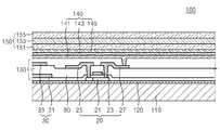
도 8은 도 1에 도시된 표시 패널(100)의 일 화소의 화소 회로(PC)를 나타내는 회로도이고, 도 9는 표시 패널(100)의 화소 구조를 나타내는 배치도이고, 도 10는 도 9의 Ⅵ-Ⅵ선에 따른 표시 패널(100)의 단면을 나타내는 단면도이다. 이하, 도 8 내지 도 10을 참조하여, 유기 발광 표시 장치의 표시 패널(100)의 내부 구조에 대해 상세히 설명한다.FIG. 8 is a circuit diagram showing a pixel circuit PC of one pixel of the
도 8을 참조하면, 본 발명의 일 실시예에 따른 유기 발광 표시 장치는 복수의 신호선에 연결되어 있으며 대략 행렬(matrix)의 형태로 배열된 복수의 화소들이 포함되어 있고, 각 화소들은 화소 회로(PC)를 갖는다. 화소는 화상을 표시하는 최소 단위를 말하며, 표시 패널(100)은 복수의 화소들을 통해 화상을 표시한다.8, an OLED display according to an exemplary embodiment of the present invention includes a plurality of pixels connected to a plurality of signal lines and arranged in the form of a matrix, PC). A pixel is a minimum unit for displaying an image, and the
각 화소에는 데이터 라인(50), 게이트 라인(40), 및 유기 발광 소자(Organic Light Emitting Diode, OLED)(140)의 일 구동전원이 되는 공통 전원 라인(60)이 구비된다. 화소 회로(PC)는 이들 데이터 라인(50), 게이트 라인(40), 및 공통 전원 라인(60)에 전기적으로 연결되어 있으며, 유기 발광 소자(140)의 발광을 제어하게 된다.Each pixel is provided with a
각 화소는 스위칭 박막 트랜지스터(10) 및 구동 박막 트랜지스터(20)의 적어도 2개의 박막 트랜지스터와, 축전 소자(30) 및 유기 발광 소자(140)를 구비한다.Each pixel includes at least two thin film transistors of the switching
상기 스위칭 박막 트랜지스터(10)는 게이트 라인(40)에 인가되는 게이트 신호에 의해 ON/OFF 되어 데이터 라인(50)에 인가되는 데이터 신호를 축전 소자(30) 및 구동 박막 트랜지스터(20)에 전달한다. 스위칭 소자로는 반드시 스위칭 박막 트랜지스터(10)만 한정되는 것은 아니며, 복수개의 박막 트랜지스터와 커패시터를 구비한 스위칭 회로가 구비될 수도 있고, 구동 박막 트랜지스터(20)의 Vth 값을 보상해주는 회로 또는, 공통 전원 라인(60)의 전압강하를 보상해주는 회로가 더 포함될 수도 있다.The switching
상기 구동 박막 트랜지스터(20)는 스위칭 박막 트랜지스터(10)를 통해 전달되는 데이터 신호에 따라, 유기 발광 소자(140)로 유입되는 전류량을 결정한다.The driving
상기 축전 소자(30)는 스위칭 박막 트랜지스터(10)를 통해 전달되는 데이터 신호를 한 프레임 동안 저장한다.The
구동 박막 트랜지스터(20) 및 스위칭 박막 트랜지스터(10)는 PMOS 박막 트랜지스터로 도시되어 있으나, 본 발명이 반드시 이에 한정되는 것은 아니며, 상기 구동 박막 트랜지스터(20) 및 스위칭 박막 트랜지스터(10) 중 적어도 하나를 NMOS 박막 트랜지스터로 형성할 수도 있음은 물론이다. 그리고, 상기와 같은 박막 트랜지스터 및 축전 소자의 개수는 반드시 이에 한정되는 것은 아니며, 이보다 더 많은 수의 박막 트랜지스터 및 축전 소자를 구비할 수 있음은 물론이다.
Although the driving
도 9 및 도 10을 함께 참조하면, 표시 패널(100)은 하나의 화소에 각각 형성된 스위칭 박막 트랜지스터(10), 구동 박막 트랜지스터(20), 축전 소자(30), 및 유기 발광 소자(140)를 포함한다. 여기서, 스위칭 박막 트랜지스터(10), 구동 박막 트랜지스터(20), 및 축전 소자(30)를 포함하는 구성을 구동 회로부(130)라 한다.9 and 10, the
또한, 표시 패널(100)은 일 방향을 따라 배치되는 게이트 라인(40), 게이트 라인(40)과 절연 교차되는 데이터 라인(50), 및 공통 전원 라인(60)을 더 포함한다. 여기서, 하나의 화소는 게이트 라인(40), 데이터 라인(50) 및 공통 전원 라인(60)을 경계로 정의될 수 있으나, 반드시 이에 한정되는 것은 아니다.The
도 9에서는, 하나의 화소에 두 개의 박막 트랜지스터(thin film transistor, TFT)와 하나의 축전 소자(capacitor)를 구비하는 2Tr-1Cap 구조의 능동 구동(active matrix, AM)형 유기 발광 표시 장치를 도시하고 있지만, 본 발명의 일 실시예가 이에 한정되는 것은 아니다.9, an active matrix (AM) type organic light emitting display device having a 2Tr-1Cap structure including two thin film transistors (TFT) and one capacitor is formed in one pixel However, the embodiment of the present invention is not limited thereto.
따라서 유기 발광 표시 장치는 하나의 화소에 셋 이상의 박막 트랜지스터와 둘 이상의 축전 소자를 구비할 수 있으며, 별도의 배선이 더 형성되어 다양한 구조를 갖도록 형성할 수도 있다.Therefore, the organic light emitting display device may have three or more thin film transistors and two or more charge accumulating elements in one pixel, or may be formed to have various structures by forming additional wiring lines.
유기 발광 소자(140)는 화소 전극(141)과, 화소 전극(141) 상에 형성된 유기 발광층(143)과, 유기 발광층(143) 상에 형성된 공통 전극(145)을 포함한다. 여기서, 화소 전극(141)은 정공 주입 전극인 양(+)극이며, 공통 전극(145)은 전자 주입 전극인 음(-)극이 된다. 그러나 본 발명의 일 실시예가 반드시 이에 한정되는 것은 아니며, 유기 발광 표시 장치의 구동 방법에 따라 화소 전극(141)이 음극이 되고, 공통 전극(145)이 양극이 될 수도 있다. 화소 전극(141) 및 공통 전극(145)으로부터 각각 정공과 전자가 유기 발광층(143) 내부로 주입된다. 주입된 정공과 전자가 결합한 엑시톤(exiton)이 여기상태로부터 기저상태로 떨어질 때 발광이 이루어진다.The organic
유기 발광층(143)은 개구 내부에 형성되어 각 화소별로 별도의 발광 물질이 형성될 수 있는데, 반드시 이에 한정되는 것은 아니며, 유기 발광층(143)은 화소의 위치에 관계 없이 전체에 공통으로 형성될 수 있다. 이때, 유기 발광층은 예를 들어, 적색, 녹색 및 청색의 빛을 방출하는 발광 물질을 포함하는 층이 수직으로 적층되거나 혼합되어 형성될 수 있다. 물론, 백색광을 방출할 수 있다면 다른 색의 조합이 가능함은 물론이다. 또한, 상기 방출된 백색광을 소정의 컬러로 변환하는 색변환층이나, 컬러 필터를 더 구비할 수 있다.The organic
또한, 본 발명의 일 실시예에 따른 유기 발광 표시 장치에서 유기 발광 소자(140)는 봉지층(150) 방향으로 빛을 방출한다. 즉, 유기 발광 소자(140)는 전면 발광형이다. 여기서, 유기 발광 소자(140)가 봉지층(150) 방향으로 빛을 방출하기 위해, 화소 전극(141)으로는 반사형 전극이 사용되고 공통 전극(145)으로는 투과형 또는 반투과형 전극이 사용된다. 그러나 본 발명의 일 실시예에서, 유기 발광 표시 장치가 전면 발광형에 한정되는 것은 아니다. 따라서, 유기 발광 표시 장치는 후면 발광형 또는 양면 발광형일 수도 있다.In addition, in the organic light emitting display according to an embodiment of the present invention, the organic
축전 소자(30)는 층간 절연막(80)을 사이에 두고 배치된 한 쌍의 축전판(31, 33)을 포함한다. 여기서, 층간 절연막(80)은 유전체가 된다. 축전 소자(30)에서 축전된 전하와 양 축전판(31, 33) 사이의 전압에 의해 축전용량이 결정된다.The capacitor element (30) includes a pair of capacitor plates (31, 33) sandwiching an interlayer insulating film (80) therebetween. Here, the
스위칭 박막 트랜지스터(10)는 스위칭 반도체층(11), 스위칭 게이트 전극(13), 스위칭 소스 전극(15), 및 스위칭 드레인 전극(17)을 포함한다. 구동 박막 트랜지스터(20)는 구동 반도체층(21), 구동 게이트 전극(23), 구동 소스 전극(25), 및 구동 드레인 전극(27)을 포함한다.The switching
또한, 도 10에서는, 탑(top) 게이트 구조의 박막 트랜지스터를 도시하고 있으나, 본 발명의 일 실시예가 이에 한정되는 것은 아니다. 따라서, 바텀(bottom) 게이트 구조의 박막 트랜지스터가 사용될 수도 있다. 또한, 스위칭 반도체층(11) 및 구동 반도체층(21)은 다결정 실리콘으로 형성될 수 있는데, 반드시 이에 한정되는 것은 아니며, 산화물 반도체로 형성될 수 있다. 예를 들어, 산화물 반도체는 아연(Zn), 인듐(In), 갈륨(Ga), 주석(Sn) 카드뮴(Cd), 게르마늄(Ge), 또는 하프늄(Hf) 과 같은 12, 13, 14족 금속 원소 및 이들의 조합에서 선택된 물질의 산화물을 포함할 수 있다. 예를 들면 반도체 활성층(212)은 G-I-Z-O[(In2O3)a(Ga2O3)b(ZnO)c](a, b, c는 각각 a≥0, b≥0, c>0의 조건을 만족시키는 실수)을 포함할 수 있다.In addition, although FIG. 10 shows a top gate structure of a thin film transistor, the embodiment of the present invention is not limited thereto. Therefore, a thin film transistor having a bottom gate structure may be used. In addition, the switching
스위칭 박막 트랜지스터(10)는 발광시키고자 하는 화소를 선택하는 스위칭 소자로 사용된다. 스위칭 게이트 전극(13)은 게이트 라인(40)에 연결된다. 스위칭 소스 전극(15)은 데이터 라인(50)에 연결된다. 스위칭 드레인 전극(17)은 스위칭 소스 전극(15)으로부터 이격 배치되며 어느 한 축전판(31)과 연결된다.The switching
구동 박막 트랜지스터(20)는 선택된 화소 내의 유기 발광 소자(140)의 유기 발광층(143)을 발광시키기 위한 구동 전원을 화소 전극(141)에 인가한다. 구동 게이트 전극(23)은 스위칭 드레인 전극(17)과 연결된 축전판(31)과 연결된다. 구동 소스 전극(25) 및 다른 한 축전판(33)은 각각 공통 전원 라인(60)과 연결된다. 구동 드레인 전극(27)은 컨택홀(contact hole)을 통해 유기 발광 소자(140)의 화소 전극(141)과 연결된다.The driving
이와 같은 구조에 의하여, 스위칭 박막 트랜지스터(10)는 게이트 라인(40)에 인가되는 게이트 전압에 의해 작동하여 데이터 라인(50)에 인가되는 데이터 전압을 구동 박막 트랜지스터(20)로 전달하는 역할을 한다. 공통 전원 라인(60)으로부터 구동 박막 트랜지스터(20)에 인가되는 공통 전압과 스위칭 박막 트랜지스터(10)로부터 전달된 데이터 전압의 차에 해당하는 전압이 축전 소자(30)에 저장되고, 축전 소자(30)에 저장된 전압에 대응하는 전류가 구동 박막 트랜지스터(20)를 통해 유기 발광 소자(140)로 흘러 유기 발광 소자(140)가 발광하게 된다.The switching
유기 발광 소자(140) 상에는, 도 10에 도시한 바와 같이, 봉지층(150)이 배치되어 유기 발광 소자(140) 및 구동 회로부(130)를 보호한다. 봉지층(150)은 하나 이상의 유기층(153)과 하나 이상의 무기층(151, 155)이 상호 교번하여 적층 형성될 수 있다.10, an
상기 무기층(151) 또는 상기 유기층(153)은 각각 복수 개일 수 있다.Each of the
상기 도면들에 도시된 구성요소들은 설명의 편의상 확대 또는 축소되어 표시될 수 있으므로, 도면에 도시된 구성요소들의 크기나 형상에 본 발명이 구속되는 것은 아니며, 본 기술 분야의 통상의 지식을 가진 자라면 이로부터 다양한 변형 및 균등한 다른 실시예가 가능하다는 점을 이해할 것이다. 따라서 본 발명의 진정한 기술적 보호범위는 첨부된 특허청구범위의 기술적 사상에 의하여 정해져야 할 것이다.It is to be understood that both the foregoing general description and the following detailed description are exemplary and explanatory and are not restrictive of the invention, It will be understood that various modifications and equivalent embodiments may be possible. Accordingly, the true scope of the present invention should be determined by the technical idea of the appended claims.
100: 표시 패널110: 가요성 기판
120: 베리어막130: 구동 회로부
140: 유기 발광 소자150: 봉지층
200, 200a, 200b, 200c, 200d, 200e: 제1 보호막
210, 310: 점착층220, 220a, 220b, 220c, 220d, 320: 보강층
230, 330: 수지층300, 300a, 300b: 제2 보호막100: display panel 110: flexible substrate
120: a barrier film 130:
140: organic light emitting device 150: sealing layer
200, 200a, 200b, 200c, 200d, 200e:
210, 310:
230, 330:
Claims (23)
Translated fromKorean상기 표시 패널이 실장되는 베젤; 및
상기 표시 패널의 하면과 상기 베젤 사이에 배치되는 완충부재;
를 포함하며,
상기 완충부재는 주변 완충부재 및 상기 주변 완충부재에 의해 에워싸이며 계단 형상의 구조를 갖는 중심 완충부재;
를 포함하는 유기 발광 표시 장치.Display panel;
A bezel on which the display panel is mounted; And
A buffer member disposed between the lower surface of the display panel and the bezel;
/ RTI >
Wherein the buffer member is surrounded by the peripheral buffer member and the peripheral buffer member and has a stepped structure;
And an organic light emitting diode (OLED).
상기 중심 완충부재는 상기 표시 패널의 하면에서 상기 베젤 쪽으로 갈수록 폭이 더 좁아지는 것을 특징으로 하는 유기 발광 표시 장치.The method according to claim 1,
Wherein the central buffering member is narrower in width from the lower surface of the display panel toward the bezel.
상기 주변 완충부재와 상기 중심 완충부재는 서로 이격되어 배치되는 것을 특징으로 하는 유기 발광 표시 장치.The method according to claim 1,
Wherein the peripheral buffer member and the center buffer member are spaced apart from each other.
상기 중심 완충부재는,
상기 표시 패널의 하면에 배치되는 제1 중심 완충부재; 및
상기 제1 중심 완충부재의 하면 상에 배치되는 제2 중심 완충부재;
를 포함하며, 상기 제2 중심 완충부재의 폭은 상기 제1 중심 완충부재의 폭보다 더 좁은 것을 특징으로 하는 유기 발광 표시 장치.The method according to claim 1,
The center cushioning member,
A first center buffering member disposed on a lower surface of the display panel; And
A second center buffer member disposed on a lower surface of the first center buffer member;
Wherein the width of the second central buffering member is narrower than the width of the first central buffering member.
상기 제2 중심 완충부재의 하면 상에 배치되는 제3 중심 완충부재;
를 더 포함하며, 상기 제3 중심 완충부재의 폭은 상기 제2 중심 완충부재의 폭보다 더 좁은 것을 특징으로 하는 유기 발광 표시 장치.5. The method of claim 4,
A third central buffering member disposed on a lower surface of the second central buffering member;
Wherein the width of the third central buffering member is narrower than the width of the second central buffering member.
상기 주변 완충부재의 일측면과 상기 중심 완충부재의 일측면은 서로 접하는 것을 특징으로 하는 유기 발광 표시 장치.The method according to claim 1,
Wherein one side of the peripheral buffer member and one side of the center buffer member are in contact with each other.
상기 완충부재는,
상기 기판과 상기 주변 완충부재 사이, 및 상기 기판과 상기 중심 완충부재 사이에 배치되는 제1 점착층;
을 포함하는 것을 특징으로 하는 유기 발광 표시 장치.The method according to claim 1,
The cushioning member,
A first adhesive layer disposed between the substrate and the peripheral buffer member, and between the substrate and the central buffer member;
And an organic light emitting diode (OLED).
상기 완충부재는,
상기 주변 완충부재의 하면에 배치되는 제2 점착층;
을 더 포함하는 것을 특징으로 하는 유기 발광 표시 장치.The method according to claim 1,
The cushioning member,
A second adhesive layer disposed on a lower surface of the peripheral buffer member;
The organic light emitting display according to claim 1,
상기 제2 점착층은,
도전성 점착층인 것을 특징으로 하는 유기 발광 표시 장치.9. The method of claim 8,
Wherein the second adhesive layer comprises:
Wherein the conductive adhesive layer is a conductive adhesive layer.
상기 제2 점착층의 하면 및 상기 중심 완충부재의 하면은, 상기 베젤과 접하는 것을 특징으로 하는 유기 발광 표시 장치.9. The method of claim 8,
Wherein a bottom surface of the second adhesive layer and a bottom surface of the center buffer member are in contact with the bezel.
상기 주변 완충부재는,
스펀지 또는 우레탄 인 것을 특징으로 하는 유기 발광 표시 장치.The method according to claim 1,
The peripheral cushioning member
Sponge or urethane.
상기 중심 완충부재는,
실리콘, 폴리에틸렌(PET) 필름, 또는 러버(Rubber) 인 것을 특징으로 하는 유기 발광 표시 장치.The method according to claim 1,
The center cushioning member,
Wherein the organic light emitting display device is a silicon, a polyethylene (PET) film, or a rubber.
상기 표시 패널은,
기판;
상기 기판 상에 형성되며 박막 트랜지스터를 포함하는 구동 회로부;
상기 기판 상에 형성되며 상기 구동 회로부와 연결된 유기 발광 소자; 및
상기 기판 상에 형성되며 상기 유기 발광 소자 및 상기 구동 회로부를 덮는 봉지층;
을 포함하는 것을 특징으로 하는 유기 발광 표시 장치.The method according to claim 1,
In the display panel,
Board;
A driving circuit formed on the substrate and including a thin film transistor;
An organic light emitting diode formed on the substrate and connected to the driving circuit; And
A sealing layer formed on the substrate and covering the organic light emitting device and the driving circuit;
And an organic light emitting diode (OLED).
상기 베젤은,
상기 표시 패널이 실장되는 바닥부; 및
상기 바닥부의 가장자리로부터 연장되어 상기 표시 패널의 측면과 마주하는 측벽;
을 포함하는 것을 특징으로 하는 유기 발광 표시 장치.The method according to claim 1,
The bezel
A bottom portion on which the display panel is mounted; And
A side wall extending from an edge of the bottom portion and facing a side surface of the display panel;
And an organic light emitting diode (OLED).
상기 표시 패널의 상부 및 상기 베젤의 상부를 덮도록 형성된 투과부;
를 더 포함하는 것을 특징으로 하는 유기 발광 표시 장치.The method according to claim 1,
A transmissive portion formed to cover an upper portion of the display panel and an upper portion of the bezel;
Wherein the organic light emitting display device further comprises an organic light emitting diode.
상기 표시 패널이 실장되는 베젤; 및
상기 표시 패널의 하면과 상기 베젤 사이에 배치되는 완충부재;
를 포함하며,
상기 완충부재는 주변 완충부재 및 상기 주변 완충부재에 의해 에워싸이며 하단부가 볼록한 곡면 형상을 갖는 중심 완충부재;
를 포함하는 유기 발광 표시 장치.Display panel;
A bezel on which the display panel is mounted; And
A buffer member disposed between the lower surface of the display panel and the bezel;
/ RTI >
Wherein the buffering member is surrounded by the peripheral buffering member and the peripheral buffering member and has a curved shape whose lower end is convex;
And an organic light emitting diode (OLED).
상기 주변 완충부재와 상기 중심 완충부재는 서로 이격되어 배치되는 것을 특징으로 하는 유기 발광 표시 장치.17. The method of claim 16,
Wherein the peripheral buffer member and the center buffer member are spaced apart from each other.
상기 완충부재는,
상기 기판과 상기 주변 완충부재 사이, 및 상기 기판과 상기 중심 완충부재 사이에 배치되는 제1 점착층;
을 포함하는 것을 특징으로 하는 유기 발광 표시 장치.17. The method of claim 16,
The cushioning member,
A first adhesive layer disposed between the substrate and the peripheral buffer member, and between the substrate and the central buffer member;
And an organic light emitting diode (OLED).
상기 완충부재는,
상기 주변 완충부재의 하면에 배치되는 제2 점착층;
을 더 포함하는 것을 특징으로 하는 유기 발광 표시 장치.17. The method of claim 16,
The cushioning member,
A second adhesive layer disposed on a lower surface of the peripheral buffer member;
The organic light emitting display according to claim 1,
상기 제2 점착층의 하면 및 상기 중심 완충부재의 하면은, 상기 베젤과 접하는 것을 특징으로 하는 유기 발광 표시 장치.20. The method of claim 19,
Wherein a bottom surface of the second adhesive layer and a bottom surface of the center buffer member are in contact with the bezel.
상기 중심 완충부재의 최하단까지의 두께는, 상기 주변 완충부재의 두께 및 상기 제2 점착층의 두께의 합보다 더 큰 것을 특징으로 하는 유기 발광 표시 장치.20. The method of claim 19,
Wherein the thickness of the center buffer member to the lowermost end is greater than the sum of the thickness of the peripheral buffer member and the thickness of the second adhesive layer.
상기 주변 완충부재는,
스펀지 또는 우레탄 인 것을 특징으로 하는 유기 발광 표시 장치.17. The method of claim 16,
The peripheral cushioning member
Sponge or urethane.
상기 중심 완충부재는,
실리콘, 폴리에틸렌(PET) 필름, 또는 러버(Rubber) 인 것을 특징으로 하는 유기 발광 표시 장치.17. The method of claim 16,
The center cushioning member,
Wherein the organic light emitting display device is a silicon, a polyethylene (PET) film, or a rubber.
Priority Applications (4)
| Application Number | Priority Date | Filing Date | Title |
|---|---|---|---|
| KR1020130065467AKR102061793B1 (en) | 2013-06-07 | 2013-06-07 | Organic light emitting diode display |
| US14/093,635US9246125B2 (en) | 2013-06-07 | 2013-12-02 | Organic light-emitting diode display |
| TW103113603ATWI625854B (en) | 2013-06-07 | 2014-04-14 | Organic light emitting diode display |
| CN201410159516.0ACN104241321B (en) | 2013-06-07 | 2014-04-21 | Organic light emitting diode display |
Applications Claiming Priority (1)
| Application Number | Priority Date | Filing Date | Title |
|---|---|---|---|
| KR1020130065467AKR102061793B1 (en) | 2013-06-07 | 2013-06-07 | Organic light emitting diode display |
Publications (2)
| Publication Number | Publication Date |
|---|---|
| KR20140143634Atrue KR20140143634A (en) | 2014-12-17 |
| KR102061793B1 KR102061793B1 (en) | 2020-01-03 |
Family
ID=52005027
Family Applications (1)
| Application Number | Title | Priority Date | Filing Date |
|---|---|---|---|
| KR1020130065467AActiveKR102061793B1 (en) | 2013-06-07 | 2013-06-07 | Organic light emitting diode display |
Country Status (4)
| Country | Link |
|---|---|
| US (1) | US9246125B2 (en) |
| KR (1) | KR102061793B1 (en) |
| CN (1) | CN104241321B (en) |
| TW (1) | TWI625854B (en) |
Families Citing this family (3)
| Publication number | Priority date | Publication date | Assignee | Title |
|---|---|---|---|---|
| KR102073884B1 (en)* | 2013-04-26 | 2020-02-06 | 삼성디스플레이 주식회사 | Organic light emitting diode display |
| CN104269429B (en)* | 2014-09-19 | 2017-05-31 | 京东方科技集团股份有限公司 | A kind of organic elctroluminescent device, its driving method and display device |
| KR102343283B1 (en)* | 2017-08-21 | 2021-12-27 | 삼성디스플레이 주식회사 | Display apparatus |
Citations (2)
| Publication number | Priority date | Publication date | Assignee | Title |
|---|---|---|---|---|
| KR20110112124A (en)* | 2010-04-06 | 2011-10-12 | 삼성모바일디스플레이주식회사 | OLED display and electronic device having same |
| KR20120079677A (en)* | 2011-01-05 | 2012-07-13 | 삼성모바일디스플레이주식회사 | Organic light emitting diode display |
Family Cites Families (11)
| Publication number | Priority date | Publication date | Assignee | Title |
|---|---|---|---|---|
| US7960913B2 (en)* | 2008-01-09 | 2011-06-14 | Samsung Mobile Display Co., Ltd. | Organic light emitting diode display device having a second bezel |
| KR100922358B1 (en) | 2008-02-28 | 2009-10-19 | 삼성모바일디스플레이주식회사 | Organic light emitting display device and electronic device having same |
| KR100927723B1 (en)* | 2008-04-10 | 2009-11-18 | 삼성모바일디스플레이주식회사 | OLED display and manufacturing method thereof |
| KR100965257B1 (en)* | 2008-10-27 | 2010-06-22 | 삼성모바일디스플레이주식회사 | Organic light emitting display and manufacturing method thereof |
| TWI462634B (en)* | 2009-04-24 | 2014-11-21 | Chi Mei El Corp | Organic light emitting diode (oled) cover substrate, display panel and manufacturing method |
| CN101699336B (en)* | 2009-10-12 | 2012-05-30 | 深超光电(深圳)有限公司 | Liquid crystal display device and manufacturing method thereof |
| KR101329456B1 (en)* | 2009-11-06 | 2013-11-15 | 엘지디스플레이 주식회사 | Organic Light Emitting Diode And Manufacturing Method Of The Same |
| KR20120028418A (en)* | 2010-09-14 | 2012-03-23 | 삼성모바일디스플레이주식회사 | Method for manufacturing encapsulated substrate using organic luminescence display device and encapsulated substrate using organic luminescence display device |
| KR20120038265A (en) | 2010-10-13 | 2012-04-23 | 삼성모바일디스플레이주식회사 | Manufacturing method of display device and assembling device for manufacturing of the display device |
| KR101857251B1 (en) | 2011-02-22 | 2018-05-14 | 삼성디스플레이 주식회사 | Flat display device |
| KR20120096353A (en)* | 2011-02-22 | 2012-08-30 | 삼성디스플레이 주식회사 | Electronic device having organic light emitting display |
- 2013
- 2013-06-07KRKR1020130065467Apatent/KR102061793B1/enactiveActive
- 2013-12-02USUS14/093,635patent/US9246125B2/enactiveActive
- 2014
- 2014-04-14TWTW103113603Apatent/TWI625854B/enactive
- 2014-04-21CNCN201410159516.0Apatent/CN104241321B/enactiveActive
Patent Citations (2)
| Publication number | Priority date | Publication date | Assignee | Title |
|---|---|---|---|---|
| KR20110112124A (en)* | 2010-04-06 | 2011-10-12 | 삼성모바일디스플레이주식회사 | OLED display and electronic device having same |
| KR20120079677A (en)* | 2011-01-05 | 2012-07-13 | 삼성모바일디스플레이주식회사 | Organic light emitting diode display |
Also Published As
| Publication number | Publication date |
|---|---|
| KR102061793B1 (en) | 2020-01-03 |
| US9246125B2 (en) | 2016-01-26 |
| CN104241321B (en) | 2019-08-16 |
| TW201501286A (en) | 2015-01-01 |
| CN104241321A (en) | 2014-12-24 |
| TWI625854B (en) | 2018-06-01 |
| US20140361958A1 (en) | 2014-12-11 |
Similar Documents
| Publication | Publication Date | Title |
|---|---|---|
| US10388711B2 (en) | Light emitting element display device | |
| US8004178B2 (en) | Organic light emitting diode display with a power line in a non-pixel region | |
| CN111326554A (en) | Display device | |
| KR101832410B1 (en) | Organic light emitting diode display | |
| KR102722115B1 (en) | Organic light emitting diode display device and method of manufacturing the same | |
| KR20170071659A (en) | flexible display device | |
| KR20110111746A (en) | Organic light emitting display | |
| CN101221974A (en) | Organic Electroluminescent Display Device | |
| CN112166465B (en) | Display device and array substrate | |
| KR20170107620A (en) | Organic light emitting display and electronic device including the same | |
| KR20110054464A (en) | Display device | |
| US10950822B2 (en) | Display device capable of improving light extraction efficiency | |
| US20210384260A1 (en) | Display panel | |
| CN104377313A (en) | Organic light emitting diode display | |
| KR102061793B1 (en) | Organic light emitting diode display | |
| CN102237391A (en) | Organic light emitting display device | |
| JP2005128310A (en) | Display device and electronic device | |
| US20210134925A1 (en) | Organic light emitting diode display device | |
| US11641757B2 (en) | Display panel having second substrate with barrier structure for defining open spaces that adjoin adhesive layer | |
| KR20100009912A (en) | Organic light emitting diode display | |
| US20190326379A1 (en) | Light emitting element display device | |
| US20250212607A1 (en) | Transistor and Display Device Including the Same | |
| CN217426335U (en) | Protection film and display module | |
| US20230413658A1 (en) | Display device | |
| JP2012064421A (en) | Light-emitting device and manufacturing method thereof |
Legal Events
| Date | Code | Title | Description |
|---|---|---|---|
| PA0109 | Patent application | Patent event code:PA01091R01D Comment text:Patent Application Patent event date:20130607 | |
| PG1501 | Laying open of application | ||
| PA0201 | Request for examination | Patent event code:PA02012R01D Patent event date:20180607 Comment text:Request for Examination of Application Patent event code:PA02011R01I Patent event date:20130607 Comment text:Patent Application | |
| E902 | Notification of reason for refusal | ||
| PE0902 | Notice of grounds for rejection | Comment text:Notification of reason for refusal Patent event date:20190528 Patent event code:PE09021S01D | |
| E701 | Decision to grant or registration of patent right | ||
| PE0701 | Decision of registration | Patent event code:PE07011S01D Comment text:Decision to Grant Registration Patent event date:20190926 | |
| GRNT | Written decision to grant | ||
| PR0701 | Registration of establishment | Comment text:Registration of Establishment Patent event date:20191226 Patent event code:PR07011E01D | |
| PR1002 | Payment of registration fee | Payment date:20191227 End annual number:3 Start annual number:1 | |
| PG1601 | Publication of registration | ||
| PR1001 | Payment of annual fee | Payment date:20221124 Start annual number:4 End annual number:4 | |
| PR1001 | Payment of annual fee | Payment date:20241125 Start annual number:6 End annual number:6 |