KR20140142929A - Semiconductor device and method for manufacturing the same, and micro processor, processor, system, data storage system and memory system including the semiconductor device - Google Patents
Semiconductor device and method for manufacturing the same, and micro processor, processor, system, data storage system and memory system including the semiconductor deviceDownload PDFInfo
- Publication number
- KR20140142929A KR20140142929AKR20130064700AKR20130064700AKR20140142929AKR 20140142929 AKR20140142929 AKR 20140142929AKR 20130064700 AKR20130064700 AKR 20130064700AKR 20130064700 AKR20130064700 AKR 20130064700AKR 20140142929 AKR20140142929 AKR 20140142929A
- Authority
- KR
- South Korea
- Prior art keywords
- recess
- layer
- interlayer insulating
- insulating film
- semiconductor device
- Prior art date
- Legal status (The legal status is an assumption and is not a legal conclusion. Google has not performed a legal analysis and makes no representation as to the accuracy of the status listed.)
- Ceased
Links
- 239000004065semiconductorSubstances0.000titleclaimsabstractdescription67
- 238000004519manufacturing processMethods0.000titleclaimsabstractdescription40
- 238000000034methodMethods0.000titleclaimsdescription98
- 238000013500data storageMethods0.000titleclaimsdescription13
- 239000010410layerSubstances0.000claimsabstractdescription242
- 239000011229interlayerSubstances0.000claimsabstractdescription99
- 239000000758substrateSubstances0.000claimsabstractdescription55
- 229920002120photoresistant polymerPolymers0.000claimsdescription76
- 238000003860storageMethods0.000claimsdescription75
- 230000008569processEffects0.000claimsdescription60
- 230000005291magnetic effectEffects0.000claimsdescription41
- 238000005530etchingMethods0.000claimsdescription38
- 230000004888barrier functionEffects0.000claimsdescription21
- 238000004891communicationMethods0.000claimsdescription17
- 230000005415magnetizationEffects0.000claimsdescription11
- 239000004020conductorSubstances0.000claimsdescription10
- 229910052751metalInorganic materials0.000claimsdescription9
- 239000002184metalSubstances0.000claimsdescription9
- 229920003169water-soluble polymerPolymers0.000claimsdescription9
- 238000000059patterningMethods0.000claimsdescription7
- 238000011161developmentMethods0.000claimsdescription6
- 239000012782phase change materialSubstances0.000claimsdescription4
- 239000006117anti-reflective coatingSubstances0.000claimsdescription3
- 230000007423decreaseEffects0.000claimsdescription3
- 229910044991metal oxideInorganic materials0.000claimsdescription3
- 150000004706metal oxidesChemical class0.000claimsdescription3
- 239000002356single layerSubstances0.000claimsdescription3
- 229910052721tungstenInorganic materials0.000claimsdescription3
- 229910052782aluminiumInorganic materials0.000claimsdescription2
- 230000003139buffering effectEffects0.000claimsdescription2
- 238000004364calculation methodMethods0.000claimsdescription2
- 229910052804chromiumInorganic materials0.000claimsdescription2
- 238000000605extractionMethods0.000claimsdescription2
- 239000011521glassSubstances0.000claimsdescription2
- 229910052735hafniumInorganic materials0.000claimsdescription2
- 229910052749magnesiumInorganic materials0.000claimsdescription2
- 229910052748manganeseInorganic materials0.000claimsdescription2
- 230000004044responseEffects0.000claimsdescription2
- 229910052719titaniumInorganic materials0.000claimsdescription2
- 229910052725zincInorganic materials0.000claimsdescription2
- 229910052726zirconiumInorganic materials0.000claimsdescription2
- 239000007921spraySubstances0.000claims1
- 229910021642ultra pure waterInorganic materials0.000claims1
- 239000012498ultrapure waterSubstances0.000claims1
- 238000012545processingMethods0.000description24
- 239000000463materialSubstances0.000description13
- 238000010586diagramMethods0.000description12
- 230000006870functionEffects0.000description9
- 230000000052comparative effectEffects0.000description7
- 230000006866deteriorationEffects0.000description7
- 239000003302ferromagnetic materialSubstances0.000description6
- 229910001260Pt alloyInorganic materials0.000description5
- 230000008859changeEffects0.000description5
- 239000007787solidSubstances0.000description5
- 229910045601alloyInorganic materials0.000description4
- 239000000956alloySubstances0.000description4
- 230000007547defectEffects0.000description4
- 238000000151depositionMethods0.000description4
- 230000003068static effectEffects0.000description4
- KDLHZDBZIXYQEI-UHFFFAOYSA-NPalladiumChemical compound[Pd]KDLHZDBZIXYQEI-UHFFFAOYSA-N0.000description3
- 230000000694effectsEffects0.000description3
- 150000004767nitridesChemical class0.000description3
- BASFCYQUMIYNBI-UHFFFAOYSA-NplatinumChemical compound[Pt]BASFCYQUMIYNBI-UHFFFAOYSA-N0.000description3
- 229910052814silicon oxideInorganic materials0.000description3
- 238000012546transferMethods0.000description3
- 229910020708Co—PdInorganic materials0.000description2
- 229910020707Co—PtInorganic materials0.000description2
- 229910001252Pd alloyInorganic materials0.000description2
- VYPSYNLAJGMNEJ-UHFFFAOYSA-NSilicium dioxideChemical compoundO=[Si]=OVYPSYNLAJGMNEJ-UHFFFAOYSA-N0.000description2
- 229910003481amorphous carbonInorganic materials0.000description2
- 230000008901benefitEffects0.000description2
- 230000015572biosynthetic processEffects0.000description2
- 125000003178carboxy groupChemical group[H]OC(*)=O0.000description2
- 238000005229chemical vapour depositionMethods0.000description2
- 239000000470constituentSubstances0.000description2
- 230000008021depositionEffects0.000description2
- 238000001312dry etchingMethods0.000description2
- 238000005516engineering processMethods0.000description2
- 239000011810insulating materialSubstances0.000description2
- 230000007774longtermEffects0.000description2
- 239000012528membraneSubstances0.000description2
- 229910000510noble metalInorganic materials0.000description2
- 239000000126substanceSubstances0.000description2
- WGTYBPLFGIVFAS-UHFFFAOYSA-Mtetramethylammonium hydroxideChemical compound[OH-].C[N+](C)(C)CWGTYBPLFGIVFAS-UHFFFAOYSA-M0.000description2
- VHUUQVKOLVNVRT-UHFFFAOYSA-NAmmonium hydroxideChemical compound[NH4+].[OH-]VHUUQVKOLVNVRT-UHFFFAOYSA-N0.000description1
- 229910000640Fe alloyInorganic materials0.000description1
- 229910003289NiMnInorganic materials0.000description1
- 229910019041PtMnInorganic materials0.000description1
- NRTOMJZYCJJWKI-UHFFFAOYSA-NTitanium nitrideChemical compound[Ti]#NNRTOMJZYCJJWKI-UHFFFAOYSA-N0.000description1
- 230000002159abnormal effectEffects0.000description1
- 239000002885antiferromagnetic materialSubstances0.000description1
- 230000006399behaviorEffects0.000description1
- 230000005540biological transmissionEffects0.000description1
- 150000004770chalcogenidesChemical class0.000description1
- 238000006243chemical reactionMethods0.000description1
- 239000011248coating agentSubstances0.000description1
- 238000000576coating methodMethods0.000description1
- 230000008878couplingEffects0.000description1
- 238000010168coupling processMethods0.000description1
- 238000005859coupling reactionMethods0.000description1
- 238000013461designMethods0.000description1
- 230000008034disappearanceEffects0.000description1
- 238000007667floatingMethods0.000description1
- 238000009413insulationMethods0.000description1
- 230000010354integrationEffects0.000description1
- 238000010884ion-beam techniqueMethods0.000description1
- 239000003960organic solventSubstances0.000description1
- 229910052763palladiumInorganic materials0.000description1
- 230000000149penetrating effectEffects0.000description1
- 229910052697platinumInorganic materials0.000description1
- 238000005498polishingMethods0.000description1
- 230000001502supplementing effectEffects0.000description1
- 229910052715tantalumInorganic materials0.000description1
- 125000003698tetramethyl groupChemical group[H]C([H])([H])*0.000description1
- 239000010936titaniumSubstances0.000description1
- 229910000314transition metal oxideInorganic materials0.000description1
- WFKWXMTUELFFGS-UHFFFAOYSA-NtungstenChemical compound[W]WFKWXMTUELFFGS-UHFFFAOYSA-N0.000description1
- 239000010937tungstenSubstances0.000description1
- 230000005641tunnelingEffects0.000description1
- 230000000007visual effectEffects0.000description1
- XLYOFNOQVPJJNP-UHFFFAOYSA-NwaterChemical compoundOXLYOFNOQVPJJNP-UHFFFAOYSA-N0.000description1
- 238000001039wet etchingMethods0.000description1
Images


Classifications
- H—ELECTRICITY
- H10—SEMICONDUCTOR DEVICES; ELECTRIC SOLID-STATE DEVICES NOT OTHERWISE PROVIDED FOR
- H10N—ELECTRIC SOLID-STATE DEVICES NOT OTHERWISE PROVIDED FOR
- H10N70/00—Solid-state devices having no potential barriers, and specially adapted for rectifying, amplifying, oscillating or switching
- H10N70/20—Multistable switching devices, e.g. memristors
- H—ELECTRICITY
- H01—ELECTRIC ELEMENTS
- H01L—SEMICONDUCTOR DEVICES NOT COVERED BY CLASS H10
- H01L21/00—Processes or apparatus adapted for the manufacture or treatment of semiconductor or solid state devices or of parts thereof
- H01L21/70—Manufacture or treatment of devices consisting of a plurality of solid state components formed in or on a common substrate or of parts thereof; Manufacture of integrated circuit devices or of parts thereof
- H01L21/71—Manufacture of specific parts of devices defined in group H01L21/70
- H01L21/76—Making of isolation regions between components
- H01L21/762—Dielectric regions, e.g. EPIC dielectric isolation, LOCOS; Trench refilling techniques, SOI technology, use of channel stoppers
- H01L21/76224—Dielectric regions, e.g. EPIC dielectric isolation, LOCOS; Trench refilling techniques, SOI technology, use of channel stoppers using trench refilling with dielectric materials
- H01L21/76229—Concurrent filling of a plurality of trenches having a different trench shape or dimension, e.g. rectangular and V-shaped trenches, wide and narrow trenches, shallow and deep trenches
- H—ELECTRICITY
- H01—ELECTRIC ELEMENTS
- H01L—SEMICONDUCTOR DEVICES NOT COVERED BY CLASS H10
- H01L21/00—Processes or apparatus adapted for the manufacture or treatment of semiconductor or solid state devices or of parts thereof
- H01L21/70—Manufacture or treatment of devices consisting of a plurality of solid state components formed in or on a common substrate or of parts thereof; Manufacture of integrated circuit devices or of parts thereof
- H01L21/71—Manufacture of specific parts of devices defined in group H01L21/70
- H01L21/76—Making of isolation regions between components
- H01L21/762—Dielectric regions, e.g. EPIC dielectric isolation, LOCOS; Trench refilling techniques, SOI technology, use of channel stoppers
- H01L21/76224—Dielectric regions, e.g. EPIC dielectric isolation, LOCOS; Trench refilling techniques, SOI technology, use of channel stoppers using trench refilling with dielectric materials
- H01L21/76232—Dielectric regions, e.g. EPIC dielectric isolation, LOCOS; Trench refilling techniques, SOI technology, use of channel stoppers using trench refilling with dielectric materials of trenches having a shape other than rectangular or V-shape, e.g. rounded corners, oblique or rounded trench walls
- H—ELECTRICITY
- H10—SEMICONDUCTOR DEVICES; ELECTRIC SOLID-STATE DEVICES NOT OTHERWISE PROVIDED FOR
- H10B—ELECTRONIC MEMORY DEVICES
- H10B12/00—Dynamic random access memory [DRAM] devices
- H—ELECTRICITY
- H10—SEMICONDUCTOR DEVICES; ELECTRIC SOLID-STATE DEVICES NOT OTHERWISE PROVIDED FOR
- H10N—ELECTRIC SOLID-STATE DEVICES NOT OTHERWISE PROVIDED FOR
- H10N50/00—Galvanomagnetic devices
- H10N50/01—Manufacture or treatment
- H—ELECTRICITY
- H10—SEMICONDUCTOR DEVICES; ELECTRIC SOLID-STATE DEVICES NOT OTHERWISE PROVIDED FOR
- H10N—ELECTRIC SOLID-STATE DEVICES NOT OTHERWISE PROVIDED FOR
- H10N50/00—Galvanomagnetic devices
- H10N50/10—Magnetoresistive devices
- H—ELECTRICITY
- H10—SEMICONDUCTOR DEVICES; ELECTRIC SOLID-STATE DEVICES NOT OTHERWISE PROVIDED FOR
- H10N—ELECTRIC SOLID-STATE DEVICES NOT OTHERWISE PROVIDED FOR
- H10N70/00—Solid-state devices having no potential barriers, and specially adapted for rectifying, amplifying, oscillating or switching
- H10N70/011—Manufacture or treatment of multistable switching devices
- H—ELECTRICITY
- H10—SEMICONDUCTOR DEVICES; ELECTRIC SOLID-STATE DEVICES NOT OTHERWISE PROVIDED FOR
- H10N—ELECTRIC SOLID-STATE DEVICES NOT OTHERWISE PROVIDED FOR
- H10N70/00—Solid-state devices having no potential barriers, and specially adapted for rectifying, amplifying, oscillating or switching
- H10N70/20—Multistable switching devices, e.g. memristors
- H10N70/231—Multistable switching devices, e.g. memristors based on solid-state phase change, e.g. between amorphous and crystalline phases, Ovshinsky effect
- H—ELECTRICITY
- H10—SEMICONDUCTOR DEVICES; ELECTRIC SOLID-STATE DEVICES NOT OTHERWISE PROVIDED FOR
- H10N—ELECTRIC SOLID-STATE DEVICES NOT OTHERWISE PROVIDED FOR
- H10N70/00—Solid-state devices having no potential barriers, and specially adapted for rectifying, amplifying, oscillating or switching
- H10N70/801—Constructional details of multistable switching devices
- H10N70/821—Device geometry
- H10N70/826—Device geometry adapted for essentially vertical current flow, e.g. sandwich or pillar type devices
- H—ELECTRICITY
- H10—SEMICONDUCTOR DEVICES; ELECTRIC SOLID-STATE DEVICES NOT OTHERWISE PROVIDED FOR
- H10N—ELECTRIC SOLID-STATE DEVICES NOT OTHERWISE PROVIDED FOR
- H10N70/00—Solid-state devices having no potential barriers, and specially adapted for rectifying, amplifying, oscillating or switching
- H10N70/801—Constructional details of multistable switching devices
- H10N70/881—Switching materials
- H10N70/882—Compounds of sulfur, selenium or tellurium, e.g. chalcogenides
- H—ELECTRICITY
- H10—SEMICONDUCTOR DEVICES; ELECTRIC SOLID-STATE DEVICES NOT OTHERWISE PROVIDED FOR
- H10N—ELECTRIC SOLID-STATE DEVICES NOT OTHERWISE PROVIDED FOR
- H10N70/00—Solid-state devices having no potential barriers, and specially adapted for rectifying, amplifying, oscillating or switching
- H10N70/801—Constructional details of multistable switching devices
- H10N70/881—Switching materials
- H10N70/883—Oxides or nitrides
- H10N70/8833—Binary metal oxides, e.g. TaOx
- H—ELECTRICITY
- H10—SEMICONDUCTOR DEVICES; ELECTRIC SOLID-STATE DEVICES NOT OTHERWISE PROVIDED FOR
- H10B—ELECTRONIC MEMORY DEVICES
- H10B10/00—Static random access memory [SRAM] devices
- H—ELECTRICITY
- H10—SEMICONDUCTOR DEVICES; ELECTRIC SOLID-STATE DEVICES NOT OTHERWISE PROVIDED FOR
- H10B—ELECTRONIC MEMORY DEVICES
- H10B53/00—Ferroelectric RAM [FeRAM] devices comprising ferroelectric memory capacitors
- H10B53/30—Ferroelectric RAM [FeRAM] devices comprising ferroelectric memory capacitors characterised by the memory core region
Landscapes
- Engineering & Computer Science (AREA)
- Manufacturing & Machinery (AREA)
- Physics & Mathematics (AREA)
- Condensed Matter Physics & Semiconductors (AREA)
- General Physics & Mathematics (AREA)
- Computer Hardware Design (AREA)
- Microelectronics & Electronic Packaging (AREA)
- Power Engineering (AREA)
- Mram Or Spin Memory Techniques (AREA)
- Hall/Mr Elements (AREA)
- Semiconductor Memories (AREA)
Abstract
Translated fromKoreanDescription
Translated fromKorean본 발명은 반도체 장치 및 그 제조 방법에 관한 것으로, 보다 상세하게는 인가되는 전압 또는 전류에 따라 서로 다른 저항 상태 사이에서 스위칭하는 가변 저항 소자를 포함할 수 있는 반도체 장치 및 그 제조 방법에 관한 것이다.
BACKGROUND OF THE INVENTION 1. Field of the Invention The present invention relates to a semiconductor device and a method of manufacturing the same, and more particularly, to a semiconductor device and a method of manufacturing the same that can include a variable resistance element for switching between different resistance states depending on an applied voltage or current.
최근 전자기기의 소형화, 저전력화, 고성능화, 다양화 등에 따라, 컴퓨터, 휴대용 통신기기 등 다양한 전자기기에서 정보를 저장할 수 있는 반도체 장치가 요구되고 있으며, 이에 대한 연구가 진행되고 있다. 이러한 반도체 장치로는 인가되는 전압 또는 전류에 따라 서로 다른 저항 상태 사이에서 스위칭하는 특성을 이용하여 데이터를 저장하는 반도체 장치 예컨대, RRAM(Resistive Random Access Memory), PRAM(Phase-change Random Access Memory), FRAM(Ferroelectric Random Access Memory), MRAM(Magnetic Random Access Memory), 이-퓨즈(E-fuse) 등이 있다.
2. Description of the Related Art In recent years, semiconductor devices capable of storing information in a variety of electronic devices such as computers and portable communication devices have been demanded for miniaturization, low power consumption, high performance, and diversification of electronic devices. Such a semiconductor device may be a semiconductor device, such as a resistive random access memory (RRAM), a phase-change random access memory (PRAM), or the like, for storing data by using a characteristic of switching between different resistance states according to a voltage or current to be applied. A ferroelectric random access memory (FRAM), a magnetic random access memory (MRAM), and an e-fuse.
본 발명이 해결하려는 과제는, 공정이 용이하고 장치의 특성을 향상시킬 수 있는 반도체 장치 및 그 제조 방법을 제공하는 것이다.
A problem to be solved by the present invention is to provide a semiconductor device and a method of manufacturing the same that can be easily processed and improve the characteristics of the device.
상기 과제를 해결하기 위한 본 발명의 일 실시예에 따른 반도체 장치는, 기판 상에 배치되고, 상기 기판의 일부를 노출시키는 리세스를 갖는 층간 절연막; 상기 리세스의 일부를 매립하는 하부 콘택; 및 상기 하부 콘택 상에서 적어도 상기 리세스의 나머지 공간을 매립하는 하부층, 및 상기 하부층 상에 배치되고 상기 층간 절연막 위로 돌출된 나머지층을 포함하는 가변 저항 소자를 포함한다.According to an aspect of the present invention, there is provided a semiconductor device comprising: an interlayer insulating film disposed on a substrate and having a recess for exposing a part of the substrate; A bottom contact for embedding a portion of the recess; And a variable resistance element including a lower layer that at least embeds the remaining space of the recess on the lower contact, and a remaining layer that is disposed on the lower layer and protrudes above the interlayer insulating film.
또한, 상기 과제를 해결하기 위한 본 발명의 일 실시예에 따른 반도체 장치의 제조 방법은, 기판 상에 층간 절연막을 형성하는 단계; 상기 층간 절연막을 선택적으로 식각하여 상기 기판의 일부를 노출시키는 리세스를 형성하는 단계; 상기 리세스의 일부를 매립하는 하부 콘택을 형성하는 단계; 상기 하부 콘택 상에서 적어도 상기 리세스의 나머지 공간을 매립하는 하부층, 및 상기 하부층 상에 배치되고 상기 층간 절연막 위로 돌출된 나머지층을 포함하는 가변 저항 소자를 형성하는 단계를 포함한다.According to another aspect of the present invention, there is provided a method of manufacturing a semiconductor device, including: forming an interlayer insulating film on a substrate; Selectively etching the interlayer insulating layer to form a recess exposing a portion of the substrate; Forming a bottom contact to fill a portion of the recess; Forming a variable resistance element including a lower layer at least filling the remaining space of the recess on the lower contact and a remaining layer disposed on the lower layer and protruding above the interlayer insulating layer.
또한, 상기 과제를 해결하기 위한 본 발명의 일 실시예에 따른 마이크로프로세서는, 외부로부터 명령을 포함하는 신호를 수신받아 상기 명령의 추출이나 해독, 입력이나 출력의 제어를 수행하는 제어부; 상기 제어부가 명령을 해독한 결과에 따라서 연산을 수행하는 연산부; 및 상기 연산을 수행하는 데이터, 상기 연산을 수행한 결과에 대응하는 데이터 및 상기 연산을 수행하는 데이터의 주소 중 하나 이상을 저장하는 기억부를 포함하고, 상기 기억부는, 기판 상에 배치되고, 상기 기판의 일부를 노출시키는 리세스를 갖는 층간 절연막; 상기 리세스의 일부를 매립하는 하부 콘택; 및 상기 하부 콘택 상에서 적어도 상기 리세스의 나머지 공간을 매립하는 하부층, 및 상기 하부층 상에 배치되고 상기 층간 절연막 위로 돌출된 나머지층을 포함하는 가변 저항 소자를 포함한다.According to another aspect of the present invention, there is provided a microprocessor including: a control unit for receiving a signal including an instruction from outside and controlling extraction or decoding of the instruction or input or output of the instruction; An operation unit for performing an operation according to a result of decoding the instruction by the control unit; And a storage unit that stores at least one of data for performing the operation, data corresponding to a result of performing the operation, and address of data for performing the operation, wherein the storage unit is disposed on the substrate, An interlayer insulating film having a recess for exposing a part of the interlayer insulating film; A bottom contact for embedding a portion of the recess; And a variable resistance element including a lower layer that at least embeds the remaining space of the recess on the lower contact, and a remaining layer that is disposed on the lower layer and protrudes above the interlayer insulating film.
또한, 상기 과제를 해결하기 위한 본 발명의 일 실시예에 따른 프로세서는, 외부로부터 입력된 명령에 따라 데이터를 이용하여 상기 명령에 대응하는 연산을 수행하는 코어부; 상기 연산을 수행하는 데이터, 상기 연산을 수행한 결과에 대응하는 데이터 및 상기 연산을 수행하는 데이터의 주소 중 하나 이상을 저장하는 캐시 메모리부; 및 상기 코어부와 상기 캐시 메모리부 사이에 연결되고, 상기 코어부와 상기 캐시 메모리부 사이에 데이터를 전송하는 버스 인터페이스를 포함하고, 상기 캐시 메모리부는, 기판 상에 배치되고, 상기 기판의 일부를 노출시키는 리세스를 갖는 층간 절연막; 상기 리세스의 일부를 매립하는 하부 콘택; 및 상기 하부 콘택 상에서 적어도 상기 리세스의 나머지 공간을 매립하는 하부층, 및 상기 하부층 상에 배치되고 상기 층간 절연막 위로 돌출된 나머지층을 포함하는 가변 저항 소자를 포함한다.According to another aspect of the present invention, there is provided a processor including: a core unit for performing an operation corresponding to an instruction using data according to an instruction input from the outside; A cache memory unit for storing at least one of data for performing the operation, data corresponding to a result of performing the operation, and address of data for performing the operation; And a bus interface connected between the core unit and the cache memory unit and transmitting data between the core unit and the cache memory unit, wherein the cache memory unit is disposed on the substrate, An interlayer insulating film having a recess to be exposed; A bottom contact for embedding a portion of the recess; And a variable resistance element including a lower layer that at least embeds the remaining space of the recess on the lower contact, and a remaining layer that is disposed on the lower layer and protrudes above the interlayer insulating film.
또한, 상기 과제를 해결하기 위한 본 발명의 일 실시예에 따른 시스템은, 외부로부터 입력된 명령을 해석하고 상기 명령을 해석한 결과에 따라 정보의 연산을 제어하는 프로세서; 상기 명령을 해석하기 위한 프로그램, 상기 정보를 저장하기 위한 보조기억장치; 상기 프로그램을 실행할 때 상기 프로세서가 상기 프로그램 및 상기 정보를 이용해 상기 연산을 수행할 수 있도록 상기 보조기억장치로부터 상기 프로그램 및 상기 정보를 이동시켜 저장하는 주기억장치; 및 상기 프로세서, 상기 보조기억장치 및 상기 주기억장치 중 하나 이상과 외부와의 통신을 수행하기 위한 인터페이스 장치를 포함하고, 상기 보조기억장치 및 상기 주기억장치 중 하나 이상은, 기판 상에 배치되고, 상기 기판의 일부를 노출시키는 리세스를 갖는 층간 절연막; 상기 리세스의 일부를 매립하는 하부 콘택; 및 상기 하부 콘택 상에서 적어도 상기 리세스의 나머지 공간을 매립하는 하부층, 및 상기 하부층 상에 배치되고 상기 층간 절연막 위로 돌출된 나머지층을 포함하는 가변 저항 소자를 포함한다.According to another aspect of the present invention, there is provided a system including: a processor for interpreting a command input from the outside and controlling an operation of information according to a result of analyzing the command; A program for interpreting the command, an auxiliary memory for storing the information; A main memory for moving and storing the program and the information from the auxiliary memory so that the processor can perform the calculation using the program and the information when the program is executed; And an interface device for performing communication with at least one of the processor, the auxiliary memory device, and the main memory device, wherein at least one of the auxiliary memory device and the main memory device is disposed on a substrate, An interlayer insulating film having a recess for exposing a part of the substrate; A bottom contact for embedding a portion of the recess; And a variable resistance element including a lower layer that at least embeds the remaining space of the recess on the lower contact, and a remaining layer that is disposed on the lower layer and protrudes above the interlayer insulating film.
또한, 상기 과제를 해결하기 위한 본 발명의 일 실시예에 따른 데이터 저장 시스템은, 데이터를 저장하며 공급되는 전원에 관계없이 저장된 데이터가 유지되는 저장 장치; 외부로부터 입력된 명령에 따라 상기 저장 장치의 데이터 입출력을 제어하는 컨트롤러; 상기 저장 장치와 외부 사이에 교환되는 데이터를 임시로 저장하는 임시 저장 장치; 및 상기 저장 장치, 상기 컨트롤러 및 상기 임시 저장 장치 중 하나 이상과 외부와의 통신을 수행하기 위한 인터페이스를 포함하고, 상기 저장 장치 및 상기 임시 저장 장치 중 하나 이상은, 기판 상에 배치되고, 상기 기판의 일부를 노출시키는 리세스를 갖는 층간 절연막; 상기 리세스의 일부를 매립하는 하부 콘택; 및 상기 하부 콘택 상에서 적어도 상기 리세스의 나머지 공간을 매립하는 하부층, 및 상기 하부층 상에 배치되고 상기 층간 절연막 위로 돌출된 나머지층을 포함하는 가변 저항 소자를 포함한다.According to another aspect of the present invention, there is provided a data storage system including: a storage device that stores data and maintains stored data regardless of a power supply; A controller for controlling data input / output of the storage device according to an instruction input from the outside; A temporary storage device for temporarily storing data exchanged between the storage device and the outside; And an interface for performing communication with the exterior with at least one of the storage device, the controller, and the temporary storage device, wherein at least one of the storage device and the temporary storage device is disposed on the substrate, An interlayer insulating film having a recess for exposing a part of the interlayer insulating film; A bottom contact for embedding a portion of the recess; And a variable resistance element including a lower layer that at least embeds the remaining space of the recess on the lower contact, and a remaining layer that is disposed on the lower layer and protrudes above the interlayer insulating film.
또한 상기 과제를 해결하기 위한 본 발명의 일 실시예에 따른 메모리 시스템은, 데이터를 저장하며 공급되는 전원에 관계없이 저장된 데이터가 유지되는 메모리; 외부로부터 입력된 명령에 따라 상기 메모리의 데이터 입출력을 제어하는 메모리 컨트롤러; 상기 메모리와 외부 사이에 교환되는 데이터를 버퍼링하기 위한 버퍼 메모리; 및 상기 메모리, 상기 메모리 컨트롤러 및 상기 버퍼 메모리 중 하나 이상과 외부와의 통신을 수행하기 위한 인터페이스를 포함하고, 상기 메모리 및 상기 버퍼 메모리 중 하나 이상은, 기판 상에 배치되고, 상기 기판의 일부를 노출시키는 리세스를 갖는 층간 절연막; 상기 리세스의 일부를 매립하는 하부 콘택; 및 상기 하부 콘택 상에서 적어도 상기 리세스의 나머지 공간을 매립하는 하부층, 및 상기 하부층 상에 배치되고 상기 층간 절연막 위로 돌출된 나머지층을 포함하는 가변 저항 소자를 포함한다.
According to another aspect of the present invention, there is provided a memory system including: a memory for storing data and storing stored data regardless of a power supply; A memory controller for controlling data input / output of the memory in response to a command input from the outside; A buffer memory for buffering data exchanged between the memory and the outside; And an interface for performing communication with at least one of the memory, the memory controller, and the buffer memory, wherein at least one of the memory and the buffer memory is disposed on a substrate, An interlayer insulating film having a recess to be exposed; A bottom contact for embedding a portion of the recess; And a variable resistance element including a lower layer that at least embeds the remaining space of the recess on the lower contact, and a remaining layer that is disposed on the lower layer and protrudes above the interlayer insulating film.
상술한 본 발명에 의한 반도체 장치 및 그 제조 방법에 의하면, 공정이 용이하고 장치의 특성을 향상시킬 수 있다.According to the above-described semiconductor device and its manufacturing method of the present invention, the process is easy and the characteristics of the device can be improved.
도 1은 비교예의 반도체 장치를 나타내는 단면도이다.
도 2a 내지 도 2f는 본 발명의 일 실시예에 따른 반도체 장치 및 그 제조 방법을 설명하기 위한 도면이다.
도 3a 내지 도 3d는 본 발명의 다른 일 실시예에 따른 반도체 장치 및 그 제조 방법을 설명하기 위한 도면이다.
도 4a 내지 도 4f는 리세스 형성 방법의 다른 실시예를 설명하기 위한 공정 단면도이다.
도 5a 내지 도 5f는 리세스 형성 방법의 또다른 실시예를 설명하기 위한 공정 단면도이다.
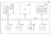
도 6은 본 발명의 일 실시예에 따른 마이크로프로세서(1000)의 구성도이다.
도 7은 본 발명의 일 실시예에 따른 프로세서(1100)의 구성도이다.
도 8은 본 발명의 일 실시예에 따른 시스템(1200)의 구성도이다.
도 9는 본 발명의 일 실시예에 따른 데이터 저장 시스템(1300)의 구성도이다.
도 10은 본 발명의 일 실시예에 따른 메모리 시스템(1400)의 구성도이다.1 is a cross-sectional view showing a semiconductor device of a comparative example.
2A to 2F are views for explaining a semiconductor device and a method of manufacturing the same according to an embodiment of the present invention.
3A to 3D are views for explaining a semiconductor device and a manufacturing method thereof according to another embodiment of the present invention.
4A to 4F are process sectional views for explaining another embodiment of the recess forming method.
5A to 5F are process cross-sectional views for explaining another embodiment of the recess forming method.
6 is a configuration diagram of a
7 is a block diagram of a
8 is a block diagram of a
9 is a configuration diagram of a
10 is a block diagram of a
이하에서는, 본 발명의 가장 바람직한 실시예가 설명된다. 도면에 있어서, 두께와 간격은 설명의 편의를 위하여 표현된 것이며, 실제 물리적 두께에 비해 과장되어 도시될 수 있다. 본 발명을 설명함에 있어서, 본 발명의 요지와 무관한 공지의 구성은 생략될 수 있다. 각 도면의 구성요소들에 참조 번호를 부가함에 있어서, 동일한 구성 요소들에 한해서는 비록 다른 도면상에 표시되더라도 가능한 한 동일한 번호를 가지도록 하고 있음에 유의하여야 한다.
Hereinafter, the most preferred embodiment of the present invention will be described. In the drawings, the thickness and the spacing are expressed for convenience of explanation, and can be exaggerated relative to the actual physical thickness. In describing the present invention, known configurations irrespective of the gist of the present invention may be omitted. It should be noted that, in the case of adding the reference numerals to the constituent elements of the drawings, the same constituent elements have the same number as much as possible even if they are displayed on different drawings.
이하, 본 발명의 실시예들을 설명하기에 앞서 이들과의 비교를 위한 반도체 장치를 도 1을 참조하여 설명하기로 한다.Hereinafter, a semiconductor device for comparison with these embodiments will be described with reference to FIG. 1 before explaining embodiments of the present invention.
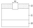
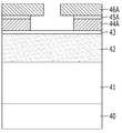
도 1은 비교예의 반도체 장치를 나타내는 단면도로서, 특히, 인가되는 전압 또는 전류에 따라 서로 다른 저항 상태 사이에서 스위칭하는 가변 저항 소자를 포함할 수 있는 반도체 장치를 나타내는 단면도이다. 나아가, 비교예의 가변 저항 소자는 자기저항 변화를 이용하는 자기저항 소자일 수 있다.Fig. 1 is a cross-sectional view showing a semiconductor device of a comparative example, in particular, a cross-sectional view showing a semiconductor device capable of including a variable resistance element for switching between different resistance states depending on an applied voltage or current. Further, the variable resistor element of the comparative example may be a magnetoresistive element that uses a change in magnetoresistance.
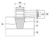
도 1을 참조하면, 비교예의 반도체 장치는, 하부 콘택(12)과 상부 콘택(17) 사이에 재개된 자기저항 소자(ME)를 포함한다.Referring to FIG. 1, the semiconductor device of the comparative example includes a magnetoresistive element (ME) resumed between the
하부 콘택(12)은 기판(10)에 형성된 소정 소자 예컨대, 스위칭 소자(미도시됨)의 일단과 연결될 수 있고, 이 스위칭 소자의 타단은 예컨대, 소스라인(미도시됨)과 연결될 수 있다. 또한, 상부 콘택(17)은 예컨대, 비트라인(18)과 연결될 수 있다. 여기서, 자기저항 소자(ME)는 하부 자성층(14A), 터널 베리어층(14B) 및 상부 자성층(14C)이 순차적으로 적층된 MTJ 구조물(14), MTJ 구조물(14)의 하부에 배치되어 하부 콘택(12)과 MTJ 구조물(14)을 연결시키면서 MTJ 구조물(14) 특성이나 공정 등을 개선하기 위한 하부층(13), MTJ 구조물(14)의 상부에 배치되어 상부 콘택(17)과 MTJ 구조물(14)을 연결시키면서 MTJ 구조물(14) 패터닝을 위한 하드마스크로 기능할 수 있는 상부층(15)을 포함할 수 있다. 또한, 설명되지 않은 도면부호 11 및 16은 층간 절연막을 나타낸다.The
이러한 반도체 장치를 제조하기 위해서는 아래와 같은 일련의 공정이 수행된다.In order to manufacture such a semiconductor device, the following series of processes are performed.
우선, 기판(10) 상에 층간 절연막(11) 및 이를 관통하는 하부 콘택(12)을 형성한 후, 그 상부에 하부층(13) 형성을 위한 도전막 및 MTJ 구조물(14) 형성을 위한 물질막 예컨대, 자성층/절연층/자성층을 형성한다. 이어서, 물질막 상에 패터닝된 상부층(15)을 형성한 후, 상부층(15)을 식각 베리어로 물질막 및 도전막을 식각하여 상부층(15)과 동일하게 패터닝된 MTJ 구조물(14) 및 하부층(13)을 형성한다. 이어서, 층간 절연막(16), 상부 콘택(17) 및 비트라인(18) 형성 공정을 수행한다.An
그런데, 이와 같이 자기저항 소자(ME)는 기본적으로 다층 구조를 갖는데다가, 최근 자기저항 소자(ME)의 요구되는 특성을 만족시키기 위해서, 자기저항 소자(ME)에 포함되는 층의 개수 또는 각 층의 두께는 계속 증가하는 추세에 있다. 반면, 반도체 장치의 집적도 증가 경향에 따라 자기저항 소자(ME) 사이의 거리는 감소하는 추세이다.As described above, the magnetoresistive element ME basically has a multi-layered structure, and in order to satisfy the required characteristics of the magnetoresistive element ME in recent years, the number of layers included in the magnetoresistive element ME, The thickness of the film is continuously increasing. On the other hand, as the degree of integration of semiconductor devices increases, the distance between the magnetoresistive elements (ME) tends to decrease.
따라서, 비교예의 반도체 장치에서 상부층(15)을 하드마스크로 MTJ 구조물(14) 및 하부층(13)까지 패터닝하기에는 하드마스크 마진이 부족한 문제가 있다. 하드마스크 마진 확보를 위해서 하부층(13)의 두께를 감소시킨다면, 아래와 같은 문제를 초래할 수 있다.Therefore, in the semiconductor device of the comparative example, there is a problem that the hard mask margin is insufficient for patterning the
비교예의 반도체 장치에서 하부층(13)은 도전막의 증착 및 평탄화 공정을 통하여 평탄한 표면을 갖도록 형성된다. 그 이유는, MTJ 구조물(14)의 터널 베리어층(14B)이 평탄도가 열악한 면 상에 형성되어 휘어지는 경우, 닐 커플링(Neel coupling) 현상 등에 의해 MTJ 구조물(14)의 특성이 열화되기 때문이다. 그런데, 하부층(13)의 패터닝을 위해 그 두께를 감소시킨다면, 평탄화 공정의 제어가 어려워진다.
In the semiconductor device of the comparative example, the
본 발명의 실시예들은, 비교예의 반도체 장치에서 발생할 수 있는 문제점들을 해결하기 위한 것이다. 이하에서 보다 상세히 설명하기로 한다.Embodiments of the present invention are intended to solve the problems that may occur in the semiconductor device of the comparative example. This will be described in more detail below.
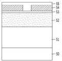
도 2a 내지 도 2f는 본 발명의 일 실시예에 따른 반도체 장치 및 그 제조 방법을 설명하기 위한 도면으로서, 도 2f는 장치를 나타내고, 도 2a 내지 도 2e는 도 2f의 장치를 제조하기 위한 중간 공정 단계의 일례를 나타낸다. 본 실시예는 가변 저항 소자로서 특히, 자기저항 소자를 포함하는 반도체 장치를 나타내고 있다.FIGS. 2A to 2F are diagrams for explaining a semiconductor device and a manufacturing method thereof according to an embodiment of the present invention, wherein FIG. 2F shows an apparatus, and FIGS. 2A to 2E show an intermediate process Fig. This embodiment shows a semiconductor device including a magnetoresistive element as a variable resistance element in particular.
도 2a를 참조하면, 요구되는 소정 구조물 예컨대, 스위칭 소자(미도시됨) 등이 형성되어 있는 기판(20)을 제공한다. 여기서, 스위칭 소자는 메모리 셀을 선택하기 위한 것으로서 예컨대, 트랜지스터, 다이오드 등일 수 있다. 스위칭 소자의 일단은 후술하는 하부 콘택과 전기적으로 연결될 수 있고, 타단은 도시되지 않은 배선 예컨대, 소스 라인과 전기적으로 연결될 수 있다.Referring to FIG. 2A, a
이어서, 기판(20) 상에 층간 절연막(21)을 형성한다. 층간 절연막(21)은 실리콘 산화물 등 다양한 절연 물질로 형성될 수 있다.Then, an
이어서, 층간 절연막(21) 상에 하부 콘택이 형성될 영역을 노출시키는 개구부를 갖는 제1 하드마스크 패턴(22)을 형성한다. 제1 하드마스크 패턴(22)의 개구부의 폭을 도면부호 W1으로 표기하였다. 이때, 개구부의 폭(W1)은 하부 콘택의 원하는 바텀(bottom) 폭과 실질적으로 동일할 수 있다.Then, a first
이러한 제1 하드마스크 패턴(22)은 층간 절연막(21)과의 식각 선택비를 갖는 막 예컨대, 포토레지스트막, 비정질 탄소막, 질화막 등으로 형성될 수 있다. 제1 하드마스크 패턴(22) 형성을 위한 식각시 과도 식각으로 인하여 제1 하드마스크 패턴(22)에 의해 드러난 층간 절연막(21)의 일부가 함께 식각될 수도 있다.The first
도 2b를 참조하면, 제1 하드마스크 패턴(22)에 의해 드러난 층간 절연막(21)의 일부를 등방성 식각하여, 층간 절연막(21) 내에 상부 리세스(23A)를 형성한다. 상부 리세스(23A)의 최상부는 제1 하드마스크 패턴(22)의 개구부의 폭(W1)보다 확장된 폭(W2)을 갖는다. 여기서, 등방성 식각은, 습식 식각 또는 화학적 반응이 활발한 건식 식각으로 수행될 수 있다.Referring to FIG. 2B, a part of the
도 2c를 참조하면, 제1 하드마스크 패턴(22)에 의해 드러난 층간 절연막(21)을 기판(20)이 노출될 때까지 이방성 식각하여 상부 리세스(23A) 아래에 위치하고 상부 리세스(23A)와 일체로 연결되는 하부 리세스(23B)를 형성한다. 이방성 식각은, 건식 식각으로 수행될 수 있다.Referring to FIG. 2C, the
도 2b 및 도 2c의 공정 결과 형성된 상부 리세스(23A) 및 하부 리세스(23B)를 리세스(23)라 하기로 한다. 리세스(23)는 후속 공정에서 하부 콘택 및 자기저항 소자의 일부가 형성될 공간을 제공하기 위한 것으로서, 전체적으로 와인 글라스 유사 형상을 가질 수 있다. 그에 따라 리세스(23)의 최상부의 폭(W2)은 최하부에 비해서 크고 아울러 제1 하드마스크 패턴(22)의 개구부의 폭(W1)보다 클 수 있다. 반면, 리세스(23)의 최하부의 폭은 제1 하드마스크 패턴(22)의 개구부의 폭(W1)과 실질적으로 동일할 수 있다. 이러한 도 2b 및 도 2c의 공정 순서는 서로 뒤바뀔 수도 있다.The
한편, 본 실시예에서는 도 2a 내지 도 2c의 공정을 통하여 와인 글라스 유사 형상의 리세스(23)를 형성하는 방법을 나타내고 있으나, 본 발명이 이에 한정되는 것은 아니다. 다양한 공정을 통하여 와인 글라스와 유사한 형상의 리세스를 형성할 수 있으며, 이에 대해서는 이하의 도 4a 내지 도 5f를 참조하여 후술하기로 한다.
Meanwhile, in this embodiment, a method of forming a
도 2d를 참조하면, 제1 하드마스크 패턴(22)을 제거한 후, 리세스(23)의 일부를 매립하는 하부 콘택(24)을 형성한다.Referring to FIG. 2D, after removing the first
구체적으로, 하부 콘택(24)은, 제1 하드마스크 패턴(22)이 제거된 결과물 상에 리세스(23)를 충분히 매립하는 두께로 도전 물질을 증착한 후, 하부 콘택(24)의 상면이 리세스(23)의 최상부보다 소정 정도(D 참조) 하향되도록 도전 물질을 에치백(etchback)함으로써 형성될 수 있다. 이때, 소정 정도(D 참조)는, 자기저항 소자의 총 두께에서 패터닝 가능한 두께를 뺀 값과 실질적으로 동일하거나 그 이상일 수 있다.Specifically, the
하부 콘택(24) 형성을 위한 도전 물질은 매립 특성이 우수하고 전기 전도도가 높은 도전 물질, 예컨대, 텅스텐(W) 또는 티타늄 질화물(TiN)일 수 있다. 또한, 도전 물질의 증착은 CVD(Chemical Vapor Deposition) 방식으로 수행될 수 있다.The conductive material for forming the
도 2e를 참조하면, 하부 콘택(24) 상에 리세스(23)의 나머지를 매립하는 하부층(25)을 형성한다.Referring to FIG. 2E, a
여기서, 하부층(25)은 자기저항 소자의 일부로서 도전 물질이기는 하나 하부 콘택(24)과 상이한 물질로 이루어질 수 있다. 하부층(25)은 하부 콘택(24)과 MTJ 구조물 사이에 개재되어 자기저항 소자의 특성이나 제조 공정을 개선하는 다양한 역할을 수행할 수 있고, 단일막 또는 다중막일 수 있다. 예컨대, 하부층(25)은 MTJ 구조물의 하부 자성층에 포함된 금속의 이상 성장을 방지하기 위한 베리어막으로의 기능을 수행할 수 있다. 또는, 하부층(25)은 상하부로 형성된 2중막일 수 있으며, 2중막 중 상부막은 MTJ 구조물의 하부 자성층의 결정도를 제어함으로써 TMR(Tunneling Magneto Resistance) 값을 조절하는 막일 수 있고, 하부막은 하부 콘택(24)과의 접착도를 증가시키면서 상부막의 막질이나 거칠기를 개선할 수 있는 버퍼막으로 기능할 수 있다. 또는, 하부층(25)은 MTJ 구조물 중 고정층의 역할을 수행하는 자성층과 반대의 자화 방향을 가짐으로써 고정층이 자유층에 끼치는 자기장의 영향을 상쇄하는 역할을 수행하는 자기 보정층을 포함할 수도 있다. 이러한 자기 보정층은 강자성(ferromagnetic) 물질 예컨대, Co 금속, Fe 금속, Fe-Pt 합금, Fe-Pd 합금, Co-Pd 합금, Co-Pt 합금, Fe-Ni-Pt 합금, Co-Fe-Pt 합금, Co-Ni-Pt 합금 등을 포함하는 단일막 또는 다중막일 수 있다. 나아가, 자기 보정층이 2 이상의 강자성 물질막을 포함하는 다중막인 경우 강자성 물질막 사이에는 백금(Pt), 팔라듐(Pd) 등과 같은 귀금속막이 개재될 수 있다. 예컨대, 자기 보정층은 강자성 물질막/귀금속막/강자성 물질막의 적층 구조를 가질 수 있다. 그러나, 본 발명이 이러한 예시에 한정되는 것은 아니며, 하부층(25)은 자기저항 소자를 포함하는 반도체 장치에서 요구되는 특성을 만족시키기 위한 다양한 기능을 갖는 막일 수 있다. 이러한 하부층(25)은 예컨대, Ti, Hf, Zr, Mn, Cr, Zn, Mg, Al, W, Ta 등과 같은 금속, 이 금속의 질화물, 또는 이 금속의 산화물을 포함할 수 있으나, 본 발명이 이러한 예시에 한정되는 것은 아니며, 다양한 물질을 포함하는 단일막 또는 다중막이 이용될 수 있다.Here, the
하부층(25)의 형성은, 하부 콘택(24)이 형성된 결과물 상에 리세스(23)를 충분히 매립하는 두께로 도전 물질을 증착한 후, 층간 절연막(21) 표면이 드러날 때까지 평탄화 공정 예컨대, CMP(Chemical Mechanical Polishing) 또는 에치백하는 방식으로 수행될 수 있다.The
본 공정 결과, 하부층(25)은 리세스(23)의 상부에 매립되게 되므로, 하부층(25)의 상면의 폭은 리세스(23)의 최상부의 폭(W2)에 대응하는 정도로 큰 값을 갖게 된다. 또한, 하부층(25)의 두께(도 2d의 D 참조)는 작을 필요가 없고, 오히려 자기저항 소자에서 패터닝이 어려운 두께 이상의 값을 가질 수 있으므로 하부층(25)의 평탄화 공정을 제어하기가 용이하다.As a result of this process, the
도 2f를 참조하면, 하부층(25) 상에 자기저항 소자에서 하부층(25)을 제외한 나머지층 예컨대, MTJ 구조물(26) 및 상부층(27)의 적층 구조물을 형성한다.Referring to FIG. 2F, a laminated structure of the remaining layers except for the
구체적으로, 도 2e의 공정 결과물 상에 MTJ 구조물(26) 형성을 위한 물질막을 형성한 후, 그 상부에 자기저항 소자 패터닝을 위한 패터닝된 상부층(27)을 형성한다. 이어서, 상부층(27)을 식각 베리어로 상기 물질막을 식각함으로써, MTJ 구조물(26)을 형성한다. 이때, MTJ 구조물(26) 형성을 위한 식각은 IBE(Ion Beam Etching) 등의 물리적 식각 방식으로 수행될 수 있다.Specifically, a material film for forming the
여기서, MTJ 구조물(26)은 예컨대, 순차적으로 적층된 하부 자성층(26A), 터널 베리어층(26B) 및 상부 자성층(26C)을 포함할 수 있다. 하부 자성층(26A) 및 상부 자성층(26C) 중 어느 하나는 자화 방향이 고정된 고정층(pinned layer)이고 다른 하나는 자화 방향이 변화되는 자유층(free layer)일 수 있다. 이러한 하부 자성층(26A) 및 상부 자성층(26C) 각각은 강자성(ferromagnetic) 물질 예컨대, Fe-Pt 합금, Fe-Pd 합금, Co-Pd 합금, Co-Pt 합금, Fe-Ni-Pt 합금, Co-Fe-Pt 합금, Co-Ni-Pt 합금 등을 포함하는 단일막 또는 다중막일 수 있으나, 본 발명이 이 예시에 한정되는 것은 아니다. 터널 베리어층(26B)은 전자가 터널링되어 하부 자성층(26A) 또는 상부 자성층(26C)의 자화 방향을 변화시키는 역할을 하는 막일 수 있다. 터널 베리어층(126B)은 예컨대, MgO, CaO, SrO, TiO, VO, NbO 등의 산화물을 포함하는 단일막 또는 다중막일 수 있으나, 본 발명이 이 예시에 한정되는 것은 아니다.Here, the
본 실시예에서는 MTJ 구조물(26)로 두 개의 자성층(26A, 26C) 사이에 터널 베리어층(26B)이 개재된 구조를 이용하고 있으나, 본 발명이 이에 한정되는 것은 아니며, MTJ 구조물(26)은 다양한 역할을 하는 층들을 더 포함할 수 있다. 예컨대, 도시하지는 않았지만, 고정층으로 작용하는 하부 자성층(26A) 또는 상부 자성층(26C)의 상부 또는 하부에는 고정층의 자화 방향을 고정시키는 역할을 수행하는 반강자성(antiferromagnetic) 물질 예컨대, FeMN,NiMn, PtMn, PdMn, PtPdMn, RuMn, OsMn, IrMn, CrPtMn 등을 포함하는 단일막 또는 다중막이 더 형성되거나, 또는 전술한 자기 보정층과 동일한 역할을 수행하는 단일막 또는 다중막이 더 형성될 수도 있다.The present invention is not limited to this structure, and the
상부층(27)은 도전성 물질로서 예컨대, 금속 또는 금속 질화물을 포함하는 단일막 또는 다중막일 수 있으나, 본 발명이 이에 한정되는 것은 아니다.The
이때, 상부층(27)은 하부층(25)과 완전히 중첩하면서 그 폭(W3)이 하부층(25) 상면의 폭(W2) 이하일 수 있다. 그에 따라, MTJ 구조물(26)은 하부층(25) 위에만 존재할 수 있다. 다시 말하면, MTJ 구조물(26)의 하면 전부는 하부층(25)과 접할 수 있다.The
본 공정 결과, 하부층(25), MTJ 구조물(26) 및 상부층(27)이 순차적으로 적층된 자기저항 소자(ME)가 형성될 수 있다.As a result of this process, the magnetoresistive device ME in which the
이어서, 본 도면에는 도시하지 않았으나, 상부층(27) 및 MTJ 구조물(26)을 덮는 절연막을 형성한 후, 절연막을 관통하여 상부층(27)과 연결되는 상부 콘택과, 절연막 상에 배치되고 상부 콘택과 연결되는 비트라인을 형성하는 등 후속 공정을 수행할 수 있다.Next, although not shown in the drawing, an upper contact, which is connected to the
이상으로 설명한 공정에 의해, 도 2f와 같은 장치가 제조될 수 있다.By the process described above, an apparatus as shown in Fig. 2F can be manufactured.
도 2f를 다시 참조하면, 본 발명의 일 실시예에 따른 반도체 장치는, 기판(20) 상에 배치되고 리세스(23)를 갖는 층간 절연막(21)과, 층간 절연막(21)의 일부를 매립하는 하부 콘택(24)과, 하부 콘택(24) 상에서 리세스(23)의 나머지를 매립하는 자기저항 소자(ME)의 하부층(25)과, 하부층(25) 상에 배치되는 자기저항 소자(ME)의 나머지층 예컨대, MTJ 구조물(26) 및 상부층(27)을 포함한다.Referring to FIG. 2F, the semiconductor device according to the embodiment of the present invention includes an
여기서, 리세스(23)는 전체적으로 와인 글라스 유사 형상을 가지며, 그에 따라 하부층(25)의 상면은 큰 폭을 가질 수 있고 MTJ 구조물(26)은 하부층(25) 위에만 존재할 수 있다.Herein, the
위와 같은 반도체 장치에서는 하부 자성층(26A) 및 상부 자성층(26C)의 자화 방향에 따라 자기저항 소자(ME)의 저항값이 달라지는 특성을 이용하여 데이터를 저장할 수 있다. 예컨대, 하부 콘택(24) 및 상부 콘택(미도시됨)을 통하여 공급되는 전류에 따라, 하부 자성층(26A) 및 상부 자성층(26C)의 자화 방향이 서로 평행하거나 또는 서로 반평행하게 된다. 자화 방향이 서로 평행한 경우 자기저항 소자(ME)는 낮은 저항 상태를 나타내어 데이터 '0'을 저장할 수 있고, 반대로 자화 방향이 서로 반평행한 경우 자기저항 소자(ME)는 높은 저항 상태를 나타내어 데이터 '1'을 저장할 수 있다.In the semiconductor device as described above, data can be stored using the characteristic that the resistance value of the magnetoresistive element ME changes according to the magnetization directions of the lower
이상으로 설명한 본 발명의 일 실시예에 따른 반도체 장치 및 그 제조 방법에 의하면 아래와 같은 이점이 있다.The semiconductor device and the method of manufacturing the same according to an embodiment of the present invention have the following advantages.
우선, 자기저항 소자(ME)의 일부인 하부층(25)이 하부 콘택(24)과 함께 리세스(23) 내에 매립되기 때문에, 하부층(25) 형성을 위한 식각이 요구되지 않는다. 따라서, 자기저항 소자(ME) 패터닝시 공정 마진이 증가할 수 있다.First, since the
또한, 하부층(25)이 리세스(23) 내에 매립된 형태를 갖기 때문에, 두께를 감소시켜야 할 필요가 없으므로 평탄화 공정을 수행하기 용이하다. 즉, 하부층(25) 상면의 평탄도를 확보할 수 있다.Further, since the
나아가, 리세스(23)의 최상부의 폭(W2)을 확장시켜 하부층(25)의 상면 폭을 확장시켰기 때문에, 정렬 마진이 증가하여 하부층(25)의 상면 전부와 접하는 MTJ 구조물(26)를 형성하는 것이 용이하다. 전술한 바와 같이 하부층(25) 상면의 평탄도가 우수하므로, MTJ 구조물(26)이 하부층(25)의 상면 전부와 접하는 경우 MTJ 구조물(26)의 터널 베리어층(26B)의 휘어짐을 방지할 수 있어 자기저항 소자(ME)의 특성을 확보할 수 있다. 만약, MTJ 구조물(26)이 하부층(25)보다 크거나 오정렬되어 층간 절연막(21) 일부와도 중첩한다면, 평탄화 공정에도 불구하고 하부층(25)과 층간 절연막(21) 경계에서 발생하는 단차에 의해서, MTJ 구조물(26)의 터널 베리어층(26B)에 굴곡이 생길 수 있는데, 본 실시예에 의하면 이러한 문제가 해결될 수 있다.
Further, since the top width W2 of the
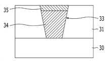
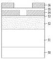
도 3a 내지 도 3d는 본 발명의 다른 일 실시예에 따른 반도체 장치 및 그 제조 방법을 설명하기 위한 도면으로서, 도 3d는 장치를 나타내고, 도 3a 내지 도 3c는 도 3d의 장치를 제조하기 위한 중간 공정 단계의 일례를 나타낸다. 이하, 전술한 실시예와의 차이점을 중심으로 설명을 진행하기로 한다.FIGS. 3A to 3D are diagrams for explaining a semiconductor device and a manufacturing method thereof according to another embodiment of the present invention, wherein FIG. 3D shows an apparatus, and FIGS. 3A to 3C are cross- An example of a process step is shown. Hereinafter, the description will be focused on differences from the above-described embodiments.
도 3a를 참조하면, 요구되는 소정 구조물 예컨대, 스위칭 소자(미도시됨) 등이 형성되어 있는 기판(30) 상에 층간 절연막(31)을 형성한다.Referring to FIG. 3A, an
이어서, 층간 절연막(31) 상에 하부 콘택이 형성될 영역을 노출시키는 개구부를 갖는 제1 하드마스크 패턴(32)을 형성한다. 이때, 제1 하드마스크 패턴(32)의 개구부의 폭(W4)은 하부 콘택의 원하는 바텀 폭보다 클 수 있고, 후술하는 하부층 상면의 원하는 폭과 대응할 수 있다.Then, a first
도 3b를 참조하면, 제1 하드마스크 패턴(32)에 의해 드러난 층간 절연막(31)을 식각하여 기판(30)을 노출시키는 리세스(33)를 형성한다. 이때, 층간 절연막(31)의 식각은 경사 식각으로 수행되며, 그에 따라 리세스(33)의 상부에서 하부로 갈수록 그 폭은 감소할 수 있다. 경사 식각은 리세스(33)의 최하부의 폭이 하부 콘택의 원하는 바텀 폭과 대응하도록 수행될 수 있다.Referring to FIG. 3B, the
도 3c를 참조하면, 제1 하드마스크 패턴(32)을 제거한 후, 리세스(33)의 일부를 매립하는 하부 콘택(34)을 형성한다.Referring to FIG. 3C, after the first
이어서, 하부 콘택(34) 상에 리세스(33)의 나머지를 매립하는 하부층(35)을 형성한다. 본 공정 결과, 하부층(35)의 상면은 리세스(33)의 최상부의 폭과 대응하는 정도로 큰 폭을 가질 수 있다.A
도 3d를 참조하면, 도 3c의 공정 결과물 상에 MTJ 구조물(36) 형성을 위한 물질막을 형성한 후, 그 상부에 자기저항 소자 패터닝을 위한 상부층(37)을 형성하고 이를 식각 베리어로 상기 물질막을 식각함으로써, MTJ 구조물(36)을 형성한다. MTJ 구조물(36)은 예컨대, 순차적으로 적층된 하부 자성층(36A), 터널 베리어층(36B) 및 상부 자성층(36C)을 포함할 수 있다. 본 공정 결과, 하부층(35), MTJ 구조물(36) 및 상부층(37)이 순차적으로 적층된 자기저항 소자(ME)가 형성될 수 있다.Referring to FIG. 3D, a material layer for forming the
전술한 실시예와 본 실시예의 차이점은, 본 실시예의 리세스(33) 형성 방법 및 그 형상에 있다. 전술한 실시예의 경우 리세스(23)를 두 번의 식각 공정으로 형성하여 와인 글라스 유사 형상을 갖게 하는 반면, 본 실시예의 경우 리세스(33)를 한 번의 식각 공정으로 형성하여 상부에서 하부로 갈수록 폭이 좁아지는 형상을 갖게 한다.The difference between the above-described embodiment and this embodiment resides in the method of forming the
그러나, 두 실시예 모두 리세스(23, 33)의 최상부의 폭을 최하부의 폭보다 크게 하고 그 일부에 하부 콘택(24, 34)을 나머지에 하부층(25, 35)을 매립한다는 점에서 공통된다. 그에 따라, 본 실시예의 발명에 의하는 경우에도 전술한 실시예에서 설명한 것과 동일한 효과를 가질 수 있다.
However, both embodiments are common in that the uppermost width of the
한편, 이상으로 설명한 실시예들에서는 자기저항 소자의 하부층 전부가 리세스 내에 매립되는 경우에 대해 설명하였으나, 본 발명이 이에 한정되는 것은 아니다. 다른 실시예에서는, 하부층의 일부가 리세스 내에 매립되고, 나머지는 층간 절연막 위로 돌출되어 있을 수도 있다. 하부층 중 리세스 내에 매립된 부분은, 리세스 상면과 동일한 평면 형상을 갖는 반면, 하부층 중 층간 절연막 위로 돌출된 부분은 상부층을 이용하여 식각되므로 상부층과 실질적으로 동일한 평면 형상을 가질 수 있다.In the above-described embodiments, all of the lower layer of the magnetoresistive element is buried in the recess, but the present invention is not limited thereto. In another embodiment, a part of the lower layer may be embedded in the recess and the remainder may protrude above the interlayer insulating film. The portion buried in the recess in the lower layer has the same planar shape as the upper surface of the recess, whereas the portion protruding above the lower interlayer insulating film is etched using the upper layer, so that it can have substantially the same planar shape as the upper layer.
나아가, 리세스 내에 매립되는 하부층 전부 또는 일부의 두께는, 자기저항 소자의 총 두께에서 패터닝 가능 두께를 뺀 값 이상이 될 있는데, 패터닝 가능 두께는 인접한 자기저항 소자 사이의 거리를 고려하여 결정할 수도 있다. 예를 들어, 자기저항 소자(ME) 패터닝이 IBE 방식에 의해 수행된다면, 인접한 자기저항 소자(ME) 사이의 거리가 100 이라 할 때 패터닝 가능한 두께는 120 정도일 수 있다. 이때 자기저항 소자(ME)의 총 두께가 120이 넘는다면 총 두께에서 패터닝 가능 두께를 뺀 나머지 부분이 리세스(23) 내에 매립될 수 있다.
Further, the thickness of all or a part of the lower layer buried in the recess may be equal to or greater than the total thickness of the magnetoresistive element minus the patternable thickness, and the patternable thickness may be determined in consideration of the distance between the adjacent magnetoresistive elements . For example, if the magnetoresistive element (ME) patterning is performed by the IBE method, the thickness that can be patterned may be 120 or so, provided that the distance between adjacent magnetoresistive elements ME is 100. [ At this time, if the total thickness of the magnetoresistive element ME exceeds 120, the remaining portion of the total thickness minus the patternable thickness can be buried in the
또한, 이상으로 설명한 실시예들에서는 자기저항 소자의 하부층이 리세스 내에 매립되는 경우에 대해 설명하였으나, 본 발명이 이에 한정되는 것은 아니며, 전술한 실시예들은 다양한 가변 저항 소자에도 적용될 수 있다.In the above-described embodiments, the lower layer of the magnetoresistive device is buried in the recess. However, the present invention is not limited thereto, and the above-described embodiments can be applied to various variable resistance devices.
예컨대, RRAM 등에 이용되는 가변 저항 소자는 도전성 하부층, 도전성 상부층 및 이들 사이에 개재된 금속 산화물을 포함할 수 있다. 금속 산화물은 예컨대, 전이 금속 산화물, 페로브스카이트(perovskite)계 물질 등을 포함할 수 있다. 이러한 가변 저항 소자는 예컨대, 공공(vacancy)의 거동에 의한 전류 필라멘트의 생성/소멸로 서로 다른 저항 상태 사이에서 스위칭하는 특성을 나타낼 수 있다.For example, the variable resistance element used in the RRAM or the like may include a conductive lower layer, a conductive upper layer, and a metal oxide interposed therebetween. The metal oxide may include, for example, transition metal oxides, perovskite-based materials, and the like. Such a variable resistive element can exhibit a characteristic of switching between different resistance states due to the generation / disappearance of current filaments due to vacancy behavior, for example.
또는, PRAM 등에 이용되는 가변 저항 소자는 도전성 하부층, 도전성 상부층 및 이들 사이에 개재된 상변화 물질을 포함할 수 있다. 상변화 물질은 예컨대, 칼코게나이드(chalcogenide)계 물질 등을 포함할 수 있다. 이러한 가변 저항 소자는 예컨대, 상변화 물질이 열에 의해 결정 상태와 비정질 상태 중 어느 하나로 안정화됨에 의하여 서로 다른 저항 상태 사이에 스위칭하는 특성을 나타낼 수 있다.Alternatively, the variable resistance element used for PRAM or the like may include a conductive lower layer, a conductive upper layer, and a phase change material interposed therebetween. The phase change material may include, for example, chalcogenide-based materials and the like. Such a variable resistive element can exhibit a characteristic that, for example, the phase-change material is switched between different resistance states by being stabilized in either the crystalline state or the amorphous state by heat.
이러한 다양한 가변 저항 소자에서, 도전성 하부층의 전부 또는 일부를 하부 콘택이 형성된 리세스의 나머지 공간에 매립되게 함으로써, 전술한 실시예들과 실질적으로 동일한 효과가 획득될 수 있다.
In these various variable resistive elements, substantially the same effect as in the above-described embodiments can be obtained by causing all or a part of the conductive lower layer to be embedded in the remaining space of the recess where the lower contact is formed.
도 4a 내지 도 4f는 리세스 형성 방법의 다른 실시예를 설명하기 위한 공정 단면도이다.4A to 4F are process sectional views for explaining another embodiment of the recess forming method.
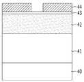
도 4a를 참조하면, 요구되는 소정 구조물 예컨대, 스위칭 소자(미도시됨) 등이 형성되어 있는 기판(40)을 제공한다.Referring to FIG. 4A, a
이어서, 기판(40) 상에 층간 절연막(41)을 형성한다. 층간 절연막(41)은 실리콘 산화물 등 다양한 절연 물질로 형성될 수 있다.Then, an
이어서, 층간 절연막(41) 상에 하드마스크층(42)을 형성한다. 하드마스크층(42)은 층간 절연막(41)과 식각 선택비를 갖는 다양한 물질을 포함하는 단일막 또는 다중막일 수 있다. 예컨대, 하드마스크층(42)은 비정질 탄소막과 SiON막이 적층된 이중막일 수 있다.Then, a
이어서, 하드마스크층(42) 상에 제1 반사방지막(43)을 형성한다. 여기서, 제1 반사방지막(43)은 BARC(Bottom Anti-Reflective Coating)막일 수 있다.Next, a
이어서, 제1 반사방지막(43) 상에 하부 콘택이 형성될 영역을 노출시키는 개구부를 갖는 제1 포토레지스트 패턴(44)을 형성한다. 제1 포토레지스트 패턴(44)의 개구부의 폭은 하부 콘택의 원하는 바텀(bottom) 폭과 실질적으로 동일할 수 있다. 이러한 제1 포토레지스트 패턴(44)은 제1 반사방지막(43) 상에 제1 포토레지스트를 도포한 후 노광 및 현상을 수행함으로써 형성될 수 있다. 노광시 제1 포토레지스트 중 빛을 받은 부분은 카르복실기(-COOH)를 포함하는 물질로 치환될 수 있다. 여기서, 현상은 NTD(Negative-Tone Development) 방식에 의할 수 있다. NTD 방식에 의하면, 유기 용제(solvent) 등과 같은 현상액을 이용함으로써 제1 포토레지스트 중 노광되지 않은 부분을 제거할 수 있는 반면, 노광된 부분은 제거되지 않고 잔류할 수 있다. 따라서, 노광시 제1 포토레지스트는 개구부에 대응하는 부분이 노광되지 않고 그외의 부분이 노광될 수 있다.Next, a
도 4b를 참조하면, 도 4a의 프로파일을 따라 제2 반사방지막(45)을 형성한다. 여기서, 제2 반사방지막(45)은 DBARC(Developer-Soluble Bottom Anti-Reflective Coating)막일 수 있다.Referring to FIG. 4B, a
이어서, 제2 반사방지막(43) 상에 제2 포토레지스트(46)를 도포한다.Subsequently, the
도 4c를 참조하면, 제2 포토레지스트(46)를 노광 및 현상하여 제2 포토레지스트 패턴(46A)을 형성한다. 제2 포토레지스트 패턴(46A)은 하부 콘택이 형성될 영역을 노출시키는 개구부를 가지며, 이 개구부의 폭은 하부 콘택의 원하는 바텀(bottom) 폭과 실질적으로 동일할 수 있다. 여기서, 현상은 PTD(Positive-Tone Development) 방식에 의할 수 있다. PTD 방식에 의하면, TMAH(Tetra MethylReferring to FIG. 4C, the
Ammonium Hydroxide) 등과 같은 현상액을 이용함으로써 제2 포토레지스트(46) 중 노광된 부분을 제거할 수 있는 반면, 노광되지 않은 부분은 제거되지 않고 잔류할 수 있다. 따라서, 노광시 제2 포토레지스트(46)는 개구부에 대응하는 부분이 노광되고 그외의 부분이 노광되지 않을 수 있다.The exposed portion of the
한편, 제2 포토레지스트(46)의 현상 과정에서, DBARC막으로 이루어진 제2 반사방지막(45)의 일부가 현상액에 의해 제거될 수 있다. 일부 제거된 제2 반사방지막(45)을 이하, 제2 반사방지막 패턴(45A)이라 한다.On the other hand, in the developing process of the
또한, 제2 포토레지스트(46)의 현상 과정에서, 제1 포토레지스트 패턴(44)의 일부가 현상액에 의해 제거될 수 있다. 제1 포토레지스트 패턴(44)은 제1 포토레지스트의 노광 공정에서 이미 빛을 받은 상태이고 제2 포토레지스트(46)의 현상은 PTD 방식으로 수행되기 때문이다. 일부 제거된 제1 포토레지스트 패턴(44)을 이하, 최종 제1 포토레지스트 패턴(44A)이라 하기로 한다. 결과적으로, 최종 제1 포토레지스트 패턴(44A)의 개구부의 폭은 제1 포토레지스트 패턴(44)의 개구부의 폭 및 제2 포토레지스트 패턴(46A)의 개구부의 폭보다 확장된다.Further, in the developing process of the
이어서, 최종 제1 포토레지스트 패턴(44A) 및 제2 포토레지스트 패턴(46A)을 식각 베리어로 기판(40)이 노출될 때까지 하드마스크층(42) 및 층간 절연막(41)을 식각한다. 이 과정에 대해서는 이하의 도 4d 내지 도 4f에 나타내었다.The
도 4d를 참조하면, 식각 초기에는 상부에 있는 제2 포토레지스트 패턴(46A)이 식각 베리어로 기능하므로, 제2 포토레지스트 패턴(46A)이 전부 손실될 때까지는 하드마스크층(42) 및/또는 층간 절연막(41)의 일부에 제2 포토레지스트 패턴(46A)의 개구부와 대응하는 홀이 형성된다.Referring to FIG. 4D, the
도 4e를 참조하면, 제2 포토레지스트 패턴(46A)이 손실된 후에는 최종 제1 포토레지스트 패턴(44A)을 식각 베리어로 하드마스크층(42) 및/또는 층간 절연막(41)이 식각된다. 이때, 최종 제1 포토레지스트 패턴(44A)의 개구부는 제2 포토레지스트 패턴(46A)의 개구부보다 크고 하드마스크층(42) 및/또는 층간 절연막(41) 중 제2 포토레지스트 패턴(46A)을 이용하여 기 식각된 부분은 그 외의 부분보다 하향되어 있으므로, 식각 과정에서 와인 글라스 유사 형상의 리세스가 형성되고 이 리세스는 점점 하향된다.Referring to FIG. 4E, after the
도 4f를 참조하면, 최종적으로 층간 절연막(41) 내에 와인 글라스 유사 형성의 리세스(R)가 형성될 수 있다.Referring to FIG. 4F, a recess (R) of wineglass-like formation may finally be formed in the
본 실시예는 전술한 실시예와 달리 한 번의 식각 공정으로 와인 글라스 유사 형상의 리세스(R) 형성이 가능하다.
In this embodiment, the recess (R) of the wineglass-like shape can be formed by one etching process unlike the above-described embodiment.
도 5a 내지 도 5f는 리세스 형성 방법의 또다른 실시예를 설명하기 위한 공정 단면도이다.5A to 5F are process cross-sectional views for explaining another embodiment of the recess forming method.
도 5a를 참조하면, 요구되는 소정 구조물 예컨대, 스위칭 소자(미도시됨) 등이 형성되어 있는 기판(50) 상에 층간 절연막(51), 하드마스크층(52) 및 반사방지막(53)을 형성한다.5A, an
이어서, 반사방지막(53) 상에 하부 콘택이 형성될 영역을 노출시키는 개구부를 갖는 제1 포토레지스트 패턴(54)을 형성한다. 제1 포토레지스트 패턴(54)의 개구부의 폭은 하부 콘택의 원하는 바텀(bottom) 폭과 실질적으로 동일할 수 있다.Subsequently, a
도 5b를 참조하면, 도 5a의 공정 결과물 상에 수용성 폴리머층(55)을 코팅 등의 방식으로 형성한다. 수용성 폴리머층(55)은 포토레지스트와 반응하지 않으므로 제1 포토레지스트 패턴(54) 및 후속 공정으로 형성되는 제2 포토레지스트 패턴에 영향을 주지 않을 수 있다. 게다가, 수용성 폴리머층(55)은 제1 포토레지스트 패턴(54)의 개구부를 용이하게 매립하면서 평탄한 표면을 가질 수 있으므로, 후속 제2 포토레지스트 패턴 형성 공정을 용이하게 수행할 수 있는 장점이 있다.Referring to FIG. 5B, a water-
도 5c를 참조하면, 수용성 폴리머층(55) 상에 제2 포토레지스트 패턴(56)을 형성한다. 제2 포토레지스트 패턴(56)의 개구부는 제1 포토레지스트 패턴(54)의 개구부와 중첩하면서 더 큰 폭을 가질 수 있다.Referring to FIG. 5C, a
도 5d를 참조하면, 제2 포토레지스트 패턴(56)에 의해 노출된 수용성 폴리머층(55)의 일부를 제거한다. 본 제거 공정은, 도 5c의 공정 결과물에 초순수(DI water)를 분사하는 방식으로 수행될 수 있다. 그 결과, 제2 포토레지스트 패턴(56)과 제2 포토레지스트 패턴(54) 사이에 개재된 수용성 폴리머 패턴(55A)이 형성된다.Referring to FIG. 5D, a portion of the water-
이어서, 제1 포토레지스트 패턴(54) 및 제2 포토레지스트 패턴(56)을 식각 베리어로 기판(50)이 노출될 때까지 하드마스크층(52) 및 층간 절연막(51)을 식각한다. 이 과정에 대해서는 이하의 도 5e 및 도 5f에 나타내었다.The
도 5e를 참조하면, 하드마스크층(52) 및 층간 절연막(51)의 식각시, 제1 포토레지스트 패턴(54)의 개구부에 의해 노출된 하드마스크층(52)부터 식각되기 시작하여 개구부에 대응하는 홀이 형성되며, 그 주변부 즉, 제1 포토레지스트 패턴(54)이 존재하고 제2 포토레지스트 패턴(56)이 존재하지 않는 부분은 상대적으로 느리게 식각된다. 그에 따라 와인 글라스 유사 형상의 리세스가 형성되고 이 리세스는 점점 하향된다.5E, when the
도 5f를 참조하면, 최종적으로 층간 절연막(51) 내에 와인 글라스 유사 형성의 리세스(R')가 형성될 수 있다.Referring to FIG. 5F, a recess (R ') of wineglass-like formation may finally be formed in the
본 실시예도 한 번의 식각 공정으로 와인 글라스 유사 형상의 리세스(R') 형성이 가능하다.In this embodiment, it is possible to form a recess (R ') of a wineglass-like shape by one etching process.
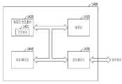
도 6은 본 발명의 일 실시예에 따른 마이크로프로세서(1000)의 구성도이다.6 is a configuration diagram of a
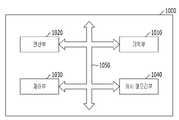
도 6에 도시된 바와 같이, 마이크로프로세서(Micro Processor Unit, 1000)는 다양한 외부 장치로부터 데이터를 받아서 처리한 후 그 결과를 외부 장치로 보내는 일련의 과정을 제어하고 조정하는 일을 수행할 수 있으며 기억부(1010), 연산부(1020) 및 제어부(1030)를 포함할 수 있다. 마이크로프로세서(1000)는 중앙 처리 장치(Central Processing Unit; CPU), 그래픽 처리 장치(Graphic Processing Unit; GPU), 디지털 신호 처리 장치(Digital Signal Processor; DSP), 어플리케이션 프로세서(Application Processor; AP) 등 각종 처리장치 일 수 있다.As shown in FIG. 6, a
기억부(1010)는 프로세서 레지스터(Processor register) 또는 레지스터(Register)로 마이크로프로세서(1000) 내에서 데이터를 저장하는 부분으로 데이터 레지스터, 주소 레지스터 및 부동 소수점 레지스터를 포함할 수 있으며 이외에 다양한 레지스터를 포함할 수 있다. 기억부(1010)는 연산부(1020)에서 연산을 수행하는 데이터나 수행결과 데이터, 수행을 위한 데이터가 저장되어 있는 주소를 일시적으로 저장하는 역할을 수행할 수 있다.The
기억부(1010)는 전술한 반도체 장치의 실시예들 중 하나를 포함할 수 있다. 전술한 실시예에 따른 반도체 장치를 포함한 기억부(1010)는 기판 상에 배치되고 기판의 일부를 노출시키는 리세스를 갖는 층간 절연막, 리세스의 일부를 매립하는 하부 콘택, 하부 콘택 상에서 적어도 리세스의 나머지 공간을 매립하는 하부층 및 하부층 상에 배치되고 층간 절연막 위로 돌출된 나머지층을 포함하는 가변 저항 소자를 포함할 수 있다. 이를 통해, 기억부(1010)의 제조 공정을 용이하게 하여 공정 불량에 기인한 신뢰성 열화를 방지할 수 있다. 결과적으로 마이크로프로세서(1000)의 제조 공정이 용이해지고 신뢰성이 향상될 수 있다.The
연산부(1020)는 마이크로프로세서(1000)의 내부에서 연산을 수행하는 부분으로 제어부(1030)가 명령을 해독한 결과에 따라서 여러 가지 사칙 연산 또는 논리 연산을 수행한다. 연산부(1020)는 하나 이상의 산술 논리 연산 장치(Arithmetic and Logic Unit; ALU)를 포함할 수 있다.The
제어부(1030)는 기억부(1010)나 연산부(1020) 및 마이크로프로세서(1000) 외부 장치로부터의 신호를 수신 받아 명령의 추출이나 해독, 입력이나 출력의 제어 등을 하고, 프로그램으로 나타내어진 처리를 실행한다.The
본 실시예에 따른 마이크로프로세서(1000)는 기억부(1010) 이외에 외부 장치로부터 입력되거나 외부 장치로 출력할 데이터를 임시 저장할 수 있는 캐시 메모리부(1040)를 추가로 포함할 수 있으며, 이 경우 버스 인터페이스(1050)를 통해 기억부(1010), 연산부(1020) 및 제어부(1030)와 데이터를 주고 받을 수 있다.
The
도 7은 본 발명의 일 실시예에 따른 프로세서(1100)의 구성도이다.7 is a block diagram of a
도 7에 도시된 바와 같이, 프로세서(1100)는 다양한 외부 장치로부터 데이터를 받아서 처리한 후 그 결과를 외부 장치로 보내는 일련의 과정을 제어하고 조정하는 일을 수행하는 마이크로프로세서 이외의 다양한 기능을 포함하여 성능 향상 및 다기능을 구현할 수 있으며 코어부(1110), 캐시 메모리부(1120) 및 버스 인터페이스(1430)를 포함할 수 있다. 본 실시예의 코어부(1110)는 외부 장치로부터 입력된 데이터를 산술 논리 연산하는 부분으로 기억부(1111), 연산부(1112), 제어부(1113)를 포함할 수 있다. 프로세서(1100)는 멀티 코어 프로세서(Multi Core Processor), 그래픽 처리 장치(Graphic Processing Unit; GPU), 어플리케이션 프로세서(Application Processor; AP) 등 각종 시스템 온 칩(System on Chip; SoC)일 수 있다.As shown in FIG. 7, the
기억부(1111)는 프로세서 레지스터(Processor register) 또는 레지스터(Register)로 프로세서(1100) 내에서 데이터를 저장하는 부분으로 데이터 레지스터, 주소 레지스터 및 부동 소수점 레지스터를 포함할 수 있으며 이외에 다양한 레지스터를 포함할 수 있다. 기억부(1111)는 연산부(1112)에서 연산을 수행하는 데이터나 수행결과 데이터, 수행을 위한 데이터가 저장되어 있는 주소를 일시적으로 저장하는 역할을 수행할 수 있다. 연산부(1112)는 프로세서(1100)의 내부에서 연산을 수행하는 부분으로 제어부(1113)가 명령을 해독한 결과에 따라서 여러 가지 사칙 연산 또는 논리 연산을 수행한다. 연산부(1112)는 하나 이상의 산술 놀리 연산 장치(Arithmetic and Logic Unit; ALU)를 포함할 수 있다. 제어부(1113)는 기억부(1111)나 연산부(1112) 및 프로세서(1100) 외부 장치로부터의 신호를 수신 받아 명령의 추출이나 해독, 입력이나 출력의 제어 등을 하고, 프로그램으로 나타내어진 처리를 실행한다.The
캐시 메모리부(1120)는 고속으로 동작하는 코어부(1110)와는 달리 저속의 외부 장치의 데이터 처리 속도 차이를 보완하기 위해 임시로 데이터를 저장하는 부분으로 1차 저장부(1121), 2차 저장부(1122) 및 3차 저장부(1123)를 포함할 수 있다. 일반적으로 캐시 메모리부(1120)는 1차, 2차 저장부(1121, 1122)를 포함하며 고용량이 필요할 경우 3차 저장부(1123)를 포함할 수 있으며, 필요시 더 많은 저장부를 포함할 수 있다. 즉 캐시 메모리부(1120)가 포함하는 저장부의 개수는 설계에 따라 달라질 수 있다. 여기서, 1차, 2차, 3차 저장부(1121, 1122, 1123)의 데이터 저장 및 판별하는 처리 속도는 같을 수도 있고 다를 수도 있다. 각 저장부의 처리 속도가 다른 경우, 1차 저장부의 속도가 제일 빠를 수 있다. 캐시 메모리부의 1차 저장부(1121), 2차 저장부(1122) 및 3차 저장부(1123) 중 어느 하나 이상의 저장부는 전술한 반도체 장치의 실시예들 중 하나를 포함할 수 있다. 전술한 실시예에 따른 반도체 장치를 포함한 캐시 메모리부(1120)는 기판 상에 배치되고 기판의 일부를 노출시키는 리세스를 갖는 층간 절연막, 리세스의 일부를 매립하는 하부 콘택, 하부 콘택 상에서 적어도 리세스의 나머지 공간을 매립하는 하부층 및 하부층 상에 배치되고 층간 절연막 위로 돌출된 나머지층을 포함하는 가변 저항 소자를 포함할 수 있다. 이를 통해, 캐시 메모리부(1120)의 제조 공정을 용이하게 하여 공정 불량에 기인한 신뢰성 열화를 방지할 수 있다. 결과적으로 프로세서(1100) 의 제조 공정이 용이해지고 신뢰성이 향상될 수 있다.도 7에는 1차, 2차, 3차 저장부(1121, 1122, 1123)가 모두 캐시 메모리부(1120)의 내부에 구성된 경우를 도시하였으나 캐시 메모리부(1120)의 1차, 2차, 3차 저장부(1121, 1122, 1123)는 모두 코어부(1110)의 외부에 구성될 수 있으며, 코어부(1110)와 외부 장치간의 처리 속도 차이를 보완할 수 있다. 또한, 캐시 메모리부(1120)의 1차 저장부(1121)는 코어부(1110)의 내부에 위치할 수 있으며 2차 저장부(1122) 및 3차 저장부(1123)는 코어부(1110)의 외부에 구성하여 처리 속도 보완을 위한 기능을 좀 더 강화시킬 수 있다.Unlike the
버스 인터페이스(1430)는 코어부(1110)와 캐시 메모리부(1120)를 연결하여 데이터를 효율적으로 전송할 수 있게 해주는 부분이다.The
본 실시예에 따른 프로세서(1100)는 다수의 코어부(1110)를 포함할 수 있으며 다수의 코어부(1110)가 캐시 메모리부(1120)를 공유할 수 있다. 다수의 코어부(1110)와 캐시 메모리부(1120)는 버스 인터페이스(1430)를 통해 연결될 수 있다. 다수의 코어부(1110)는 모두 상술한 코어부의 구성과 동일하게 구성될 수 있다. 다수의 코어부(1110)를 포함할 경우, 캐시 메모리부(1120)의 1차 저장부(1121)는 다수의 코어부(1110)의 개수에 대응하여 각각의 코어부(1110) 내에 구성되고 2차 저장부(1122)와 3차 저장부(1123)는 하나로 다수의 코어부(1110)의 외부에 버스 인터페이스(1430)를 통해 공유되도록 구성될 수 있다. 여기서, 1차 저장부(1121)의 처리 속도가 2차, 3차 저장부(1122, 1123)의 처리 속도보다 빠를 수 있다.The
본 실시예에 따른 프로세서(1100)는 데이터를 저장하는 임베디드(Embedded) 메모리부(1140), 외부 장치와 유선 또는 무선으로 데이터를 송수신 할 수 있는 통신모듈부(1150), 외부 기억 장치를 구동하는 메모리 컨트롤부(1160), 외부 인터페이스 장치에 프로세서(1100)에서 처리된 데이터나 외부 입력장치에서 입력된 데이터를 가공하고 출력하는 미디어처리부(1170)를 추가로 포함할 수 있으며, 이 이외에도 다수의 모듈을 포함할 수 있다. 이 경우 추가된 다수의 모듈들은 버스 인터페이스(1430)를 통해 코어부(1110), 캐시 메모리부(1120) 및 상호간 데이터를 주고 받을 수 있다.The
여기서 임베디드 메모리부(1140)는 휘발성 메모리뿐만 아니라 비휘발성 메모리를 포함할 수 있다. 휘발성 메모리는 DRAM(Dynamic Random Access Memory), Moblie DRAM, SRAM(Static Random Access Memory) 등을 포함할 수 있으며, 비휘발성 메모리는 ROM(Read Only Memory), Nor Flash Memory, NAND Flash Memory, 상변환 메모리(Phase Change Random Access Memory; PRAM), 저항 메모리(Resistive Random Access Memory;RRAM), 스핀 주입 메모리(Spin Transfer Torque Random Access Memory; STTRAM), 자기메모리(Magnetic Random Access Memory; MRAM) 등을 포함할 수 있다.The embedded
통신모듈부(1150)는 유선 네트워크와 연결할 수 있는 모듈과 무선 네트워크와 연결할 수 있는 모듈을 모두 포함할 수 있다. 유선 네트워크 모듈은 유선랜(Local Area Network; LAN), 유에스비(Universal Serial Bus; USB), 이더넷(Ethernet), 전력선통신(Power Line Communication; PLC) 등을 포함할 수 있으며, 무선 네트워크 모듈은 적외선 통신(Infrared Data Association; IrDA), 코드 분할 다중 접속(Code Division Multiple Access; CDMA), 시분할 다중 접속(Time Division Multiple Access; TDMA), 주파수 분할 다중 접속(Frequency Division Multiple Access; FDMA), 무선랜(Wireless LAN), 지그비(Zigbee), 유비쿼터스 센서 네트워크(Ubiquitous Sensor Network; USN), 블루투스(Bluetooth), RFID(Radio Frequency IDentification), 롱텀에볼루션(Long Term Evolution; LTE), 근거리 무선통신(Near Field Communication; NFC), 광대역 무선 인터넷(Wireless Broadband Internet; Wibro), 고속 하향 패킷 접속(High Speed Downlink Packet Access; HSDPA), 광대역 코드 분할 다중 접속(Wideband CDMA; WCDMA), 초광대역 통신(Ultra WideBand; UWB) 등을 포함할 수 있다.The
메모리 컨트롤부(1160)는 프로세서(1100)와 서로 다른 통신 규격에 따라 동작하는 외부 저장 장치 사이에 전송되는 데이터를 관리하기 위한 것으로 각종 메모리 컨트롤러, IDE(Integrated Device Electronics), SATA(Serial Advanced Technology Attachment), SCSI(Small Computer System Interface), RAID(Redundant Array of Independent Disks), SSD(Solid State Disk), eSATA(External SATA), PCMCIA(Personal Computer Memory Card International Association), USB(Universal Serial Bus), 씨큐어 디지털 카드(Secure Digital; SD), 미니 씨큐어 디지털 카드(mini Secure Digital card; mSD), 마이크로 씨큐어 디지털 카드(micro SD), 고용량 씨큐어 디지털 카드(Secure Digital High Capacity; SDHC), 메모리 스틱 카드(Memory Stick Card), 스마트 미디어 카드(Smart Media Card; SM), 멀티 미디어 카드(Multi Media Card; MMC), 내장 멀티 미디어 카드(Embedded MMC; eMMC), 컴팩트 플래시 카드(Compact Flash; CF) 등을 제어하는 컨트롤러를 포함 할 수 있다.The
미디어처리부(1170)는 프로세서(1100)에서 처리된 데이터나 외부 입력장치에서 입력된 데이터를 가공하여 영상, 음성 및 기타 형태로 전달되도록 외부 인터페이스 장치로 출력하는 그래픽 처리 장치(Graphics Processing Unit; GPU), 디지털 신호 처리 장치(Digital Signal Processor; DSP), 고선명 오디오(High Definition Audio; HD Audio), 고선명 멀티미디어 인터페이스(High Definition Multimedia Interface; HDMI) 컨트롤러 등을 포함할 수 있다.
The
도 8은 본 발명의 일 실시예에 따른 시스템(1200)의 구성도이다.8 is a block diagram of a
도 8에 도시된 바와 같이, 시스템(1200)은 데이터를 처리하는 장치로 데이터에 대하여 일련의 조작을 행하기 위해 입력, 처리, 출력, 통신, 저장 등을 수행할 수 있으며 프로세서(1210), 주기억 장치(1220), 보조기억 장치(1230), 인터페이스 장치(1240)를 포함할 수 있다. 본 실시예의 시스템은 컴퓨터(Computer), 서버(Server), PDA(Personal Digital Assistant), 휴대용 컴퓨터(Portable Computer), 웹 타블렛(Web Tablet), 무선 폰(Wireless Phone), 모바일 폰(Mobile Phone), 스마트 폰(Smart Phone), 디지털 뮤직 플레이어(Digital Music Player), PMP(Portable Multimedia Player), 카메라(Camera), 위성항법장치(Global Positioning System; GPS), 비디오 카메라(Video Camera), 음성 녹음기(Voice Recorder), 텔레매틱스(Telematics), AV시스템(Audio Visual System), 스마트 텔레비전(Smart Television) 등 프로세스를 사용하여 동작하는 각종 전자 시스템일 수 있다.As shown in FIG. 8, the
프로세서(1210)는 입력된 명령어의 해석과 시스템에 저장된 자료의 연산, 비교 등의 처리를 제어하는 시스템의 핵심적인 구성으로 마이크로프로세서(Micro Processor Unit; MPU), 중앙 처리 장치(Central Processing Unit; CPU), 싱글/멀티 코어 프로세서(Single/Multi Core Processor), 그래픽 처리 장치(Graphic Processing Unit; GPU), 어플리케이션 프로세서(Application Processor; AP), 디지털 신호 처리 장치(Digital Signal Processor; DSP) 등으로 구성할 일 수 있다.The
주기억장치(1220)는 프로그램이 실행될 때 보조기억장치(1230)로부터 프로그램이나 자료를 이동시켜 실행시킬 수 있는 기억장소로 전원이 끊어져도 기억된 내용이 보존되며 전술한 실시예에 따른 반도체 장치를 포함할 수 있다. 주기억장치는 기판 상에 배치되고 기판의 일부를 노출시키는 리세스를 갖는 층간 절연막, 리세스의 일부를 매립하는 하부 콘택, 하부 콘택 상에서 적어도 리세스의 나머지 공간을 매립하는 하부층 및 하부층 상에 배치되고 층간 절연막 위로 돌출된 나머지층을 포함하는 가변 저항 소자를 포함할 수 있다. 이를 통해, 주기억장치(1220)의 제조 공정을 용이하게 하여 공정 불량에 기인한 신뢰성 열화를 방지할 수 있다. 결과적으로 시스템(1200)의 제조 공정이 용이해지고 신뢰성이 향상될 수 있다.더불어, 주기억장치(1220)는 전원이 꺼지면 모든 내용이 지워지는 휘발성 메모리 타입의 에스램(Static Random Access Memory; SRAM), 디램(Dynamic Random Access Memory) 등을 더 포함 할 수 있다. 이와는 다르게, 주기억장치(1220)는 본 발명의 실시예에 따른 반도체 장치를 포함하지 않고 전원이 꺼지면 모든 내용이 지워지는 휘발성 메모리 타입의 에스램(Static Random Access Memory; SRAM), 디램(Dynamic Random Access Memory) 등을 포함 할 수 있다.The
보조기억장치(1230)는 프로그램 코드나 데이터를 보관하기 위한 기억장치를 말한다. 주기억장치(1220)보다 속도는 느리지만 많은 자료를 보관할 수 있으며 전술한 실시예에 따른 반도체 장치를 포함할 수 있다. 보조기억장치는 기판 상에 배치되고 기판의 일부를 노출시키는 리세스를 갖는 층간 절연막, 리세스의 일부를 매립하는 하부 콘택, 하부 콘택 상에서 적어도 리세스의 나머지 공간을 매립하는 하부층 및 하부층 상에 배치되고 층간 절연막 위로 돌출된 나머지층을 포함하는 가변 저항 소자를 포함할 수 있다. 이를 통해, 보조기억장치(1230)의 제조 공정을 용이하게 하여 공정 불량에 기인한 신뢰성 열화를 방지할 수 있다. 결과적으로 시스템(1200) 의 제조 공정이 용이해지고 신뢰성이 향상될 수 있다.더불어, 보조기억장치(1230)는 자기를 이용한 자기테이프, 자기디스크, 빛을 이용한 레이져 디스크, 이들 둘을 이용한 광자기디스크, 고상 디스크(Solid State Disk; SSD), USB메모리(Universal Serial Bus Memory; USB Memory), 씨큐어 디지털 카드(Secure Digital; SD), 미니 씨큐어 디지털 카드(mini Secure Digital card; mSD), 마이크로 씨큐어 디지털 카드(micro SD), 고용량 씨큐어 디지털 카드(Secure Digital High Capacity; SDHC), 메모리 스틱 카드(Memory Stick Card), 스마트 미디어 카드(Smart Media Card; SM), 멀티 미디어 카드(Multi Media Card; MMC), 내장 멀티 미디어 카드(Embedded MMC; eMMC), 컴팩트 플래시 카드(Compact Flash; CF) 등의 데이터 저장 시스템(도 13의 1300 참조)을 더 포함할 수 있다. 이와는 다르게, 보조기억장치(1230)는 전술한 실시예의 반도체 장치를 포함하지 않고 자기를 이용한 자기테이프, 자기디스크, 빛을 이용한 레이져 디스크, 이들 둘을 이용한 광자기디스크, 고상 디스크(Solid State Disk; SSD), USB메모리(Universal Serial Bus Memory; USB Memory), 씨큐어 디지털 카드(Secure Digital; SD), 미니 씨큐어 디지털 카드(mini Secure Digital card; mSD), 마이크로 씨큐어 디지털 카드(micro SD), 고용량 씨큐어 디지털 카드(Secure Digital High Capacity; SDHC), 메모리 스틱 카드(Memory Stick Card), 스마트 미디어 카드(Smart Media Card; SM), 멀티 미디어 카드(Multi Media Card; MMC), 내장 멀티 미디어 카드(Embedded MMC; eMMC), 컴팩트 플래시 카드(Compact Flash; CF) 등의 데이터 저장 시스템(도 13의 1300 참조)들을 포함할 수 있다.The
인터페이스 장치(1240)는 본 실시예의 시스템과 외부 장치의 명령 및 데이터 등을 교환하기 위한 것일 수 있으며, 키패드(keypad), 키보드(keyboard), 마우스(Mouse), 스피커(Speaker), 마이크(Mike), 표시장치(Display), 각종 휴먼 인터페이스 장치(Human Interface Device; HID)들 및 통신장치일 수 있다. 통신장치는 유선 네트워크와 연결할 수 있는 모듈과 무선 네트워크와 연결할 수 있는 모듈을 모두 포함할 수 있다. 유선 네트워크 모듈은 유선랜(Local Area Network; LAN), 유에스비(Universal Serial Bus; USB), 이더넷(Ethernet), 전력선통신(Power Line Communication; PLC) 등을 포함할 수 있으며, 무선 네트워크 모듈은 적외선 통신(Infrared Data Association; IrDA), 코드 분할 다중 접속(Code Division Multiple Access; CDMA), 시분할 다중 접속(Time Division Multiple Access; TDMA), 주파수 분할 다중 접속(Frequency Division Multiple Access; FDMA), 무선랜(Wireless LAN), 지그비(Zigbee), 유비쿼터스 센서 네트워크(Ubiquitous Sensor Network; USN), 블루투스(Bluetooth), RFID(Radio Frequency IDentification), 롱텀에볼루션(Long Term Evolution; LTE), 근거리 무선통신(Near Field Communication; NFC), 광대역 무선 인터넷(Wireless Broadband Internet; Wibro), 고속 하향 패킷 접속(High Speed Downlink Packet Access; HSDPA), 광대역 코드 분할 다중 접속(Wideband CDMA; WCDMA), 초광대역 통신(Ultra WideBand; UWB) 등을 포함할 수 있다.
The
도 9는 본 발명의 일 실시예에 따른 데이터 저장 시스템(1300)의 구성도이다.9 is a configuration diagram of a
도 9에 도시된 바와 같이, 데이터 저장 시스템(1300)은 데이터 저장을 위한 구성으로 비휘발성 특성을 가지는 저장 장치(1310), 이를 제어하는 컨트롤러(1320) 및 외부 장치와 연결하는 인터페이스(1330)를 포함할 수 있다. 데이터 저장 시스템(1300)은 하드 디스크(Hard Disk Drive; HDD), 광학 드라이브(Compact Disc Read Only Memory; CDROM), DVD(Digital Versatile Disc), 고상 디스크(Solid State Disk; SSD) 등의 디스크 형태와 USB메모리(Universal Serial Bus Memory; USB Memory), 씨큐어 디지털 카드(Secure Digital; SD), 미니 씨큐어 디지털 카드(mini Secure Digital card; mSD), 마이크로 씨큐어 디지털 카드(micro SD), 고용량 씨큐어 디지털 카드(Secure Digital High Capacity; SDHC), 메모리 스틱 카드(Memory Stick Card), 스마트 미디어 카드(Smart Media Card; SM), 멀티 미디어 카드(Multi Media Card; MMC), 내장 멀티 미디어 카드(Embedded MMC; eMMC), 컴팩트 플래시 카드(Compact Flash; CF) 등의 카드 형태일 수 있다.9, the
컨트롤러(1320)는 저장 장치(1310)와 인터페이스(1330) 사이에서 데이터의 교환을 제어할 수 있다. 이를 위해 컨트롤러(1320)는 데이터 저장 시스템(1300) 외부에서 인터페이스(1330)를 통해 입력된 명령어들을 연산 및 처리하기 위한 프로세서(1321)를 포함할 수 있다.The
인터페이스(1330)는 데이터 저장 시스템(1300)과 외부 장치간에 명령 및 데이터 등을 교환하기 위한 것으로 데이터 저장 시스템(1300)이 카드인 경우 USB(Universal Serial Bus Memory), 씨큐어 디지털 카드(Secure Digital; SD), 미니 씨큐어 디지털 카드(mini Secure Digital card; mSD), 마이크로 씨큐어 디지털 카드(micro SD), 고용량 씨큐어 디지털 카드(Secure Digital High Capacity; SDHC), 메모리 스틱 카드(Memory Stick Card), 스마트 미디어 카드(Smart Media Card; SM), 멀티 미디어 카드(Multi Media Card; MMC), 내장 멀티 미디어 카드(Embedded MMC; eMMC), 컴팩트 플래시 카드(Compact Flash; CF)와 호환되는 인터페이스 일 수 있다. 디스크 형태일 경우 IDE(Integrated Device Electronics), SATA(Serial Advanced Technology Attachment), SCSI(Small Computer System Interface), eSATA(External SATA), PCMCIA(Personal Computer Memory Card International Association), USB(Universal Serial Bus)와 호환되는 인터페이스일 수 있다.The
본 실시예의 데이터 저장 시스템(1300)은 외부 장치와의 인터페이스, 컨트롤러, 및 시스템의 다양화, 고성능화에 따라 인터페이스(1330)와 저장 장치(1310)간의 데이터의 전달을 효율적으로 하기 위한 임시 저장 장치(1340)를 포함할 수 있다. 저장 장치(1310) 및 데이터를 임시로 저장하는 임시 저장 장치(1340)는 전술한 실시예에 따른 반도체 장치를 포함할 수 있다. 저장 장치(1310) 또는 임시 저장 장치(1340)는 기판 상에 배치되고 기판의 일부를 노출시키는 리세스를 갖는 층간 절연막, 리세스의 일부를 매립하는 하부 콘택, 하부 콘택 상에서 적어도 리세스의 나머지 공간을 매립하는 하부층 및 하부층 상에 배치되고 층간 절연막 위로 돌출된 나머지층을 포함하는 가변 저항 소자를 포함할 수 있다. 이를 통해, 저장 장치(1310) 또는 임시 저장 장치(1340)의 제조 공정을 용이하게 하여 공정 불량에 기인한 신뢰성 열화를 방지할 수 있다. 결과적으로 데이터 저장 시스템(1300)의 제조 공정이 용이해지고 신뢰성이 향상될 수 있다.
The
도 10은 본 발명의 일 실시예에 따른 메모리 시스템(1400)의 구성도이다.10 is a block diagram of a
도 10에 도시된 바와 같이, 메모리 시스템(1400)은 데이터 저장을 위한 구성으로 비휘발성 특성을 가지는 메모리(1410), 이를 제어하는 메모리 컨트롤러(1420) 및 외부 장치와 연결하는 인터페이스(1430)를 포함할 수 있다. 메모리 시스템(1400)은 고상 디스크(Solid State Disk; SSD), USB메모리(Universal Serial Bus Memory; USB Memory), 씨큐어 디지털 카드(Secure Digital; SD), 미니 씨큐어 디지털 카드(mini Secure Digital card; mSD), 마이크로 씨큐어 디지털 카드(micro SD), 고용량 씨큐어 디지털 카드(Secure Digital High Capacity; SDHC), 메모리 스틱 카드(Memory Stick Card), 스마트 미디어 카드(Smart Media Card; SM), 멀티 미디어 카드(Multi Media Card; MMC), 내장 멀티 미디어 카드(Embedded MMC; eMMC), 컴팩트 플래시 카드(Compact Flash; CF) 등의 카드 형태일 수 있다.As shown in FIG. 10, the
데이터를 저장하는 메모리(1410)는 전술한 실시예에 따른 반도체 장치를 포함할 수 있다. 메모리(1410)는 기판 상에 배치되고 기판의 일부를 노출시키는 리세스를 갖는 층간 절연막, 리세스의 일부를 매립하는 하부 콘택, 하부 콘택 상에서 적어도 리세스의 나머지 공간을 매립하는 하부층 및 하부층 상에 배치되고 층간 절연막 위로 돌출된 나머지층을 포함하는 가변 저항 소자를 포함할 수 있다. 이를 통해, 메모리(1410)의 제조 공정을 용이하게 하여 공정 불량에 기인한 신뢰성 열화를 방지할 수 있다. 결과적으로 메모리 시스템(1400) 의 제조 공정이 용이해지고 신뢰성이 향상될 수 있다.더불어, 본 실시예의 메모리는 비휘발성인 특성을 가지는 ROM(Read Only Memory), Nor Flash Memory, NAND Flash Memory, 상변환 메모리(Phase Change Random Access Memory; PRAM), 저항 메모리(Resistive Random Access Memory;RRAM), 자기메모리(Magnetic Random Access Memory; MRAM) 등을 더 포함할 수 있다.The
메모리 컨트롤러(1420)는 메모리(1410)와 인터페이스(1430) 사이에서 데이터의 교환을 제어할 수 있다. 이를 위해 메모리 컨트롤러(1420)는 메모리 시스템(1400) 외부에서 인터페이스(1430)를 통해 입력된 명령어들을 연산 및 처리하기 위한 프로세서(1421)를 포함할 수 있다.
인터페이스(1430)는 메모리 시스템(1400)과 외부 장치간에 명령 및 데이터 등을 교환하기 위한 것으로 USB(Universal Serial Bus), 씨큐어 디지털 카드(Secure Digital; SD), 미니 씨큐어 디지털 카드(mini Secure Digital card; mSD), 마이크로 씨큐어 디지털 카드(micro SD), 고용량 씨큐어 디지털 카드(Secure Digital High Capacity; SDHC), 메모리 스틱 카드(Memory Stick Card), 스마트 미디어 카드(Smart Media Card; SM), 멀티 미디어 카드(Multi Media Card; MMC), 내장 멀티 미디어 카드(Embedded MMC; eMMC), 컴팩트 플래시 카드(Compact Flash; CF)와 호환될 수 있다.The
본 실시예의 메모리 시스템(1400)은 외부 장치와의 인터페이스, 메모리 컨트롤러, 및 메모리 시스템의 다양화, 고성능화에 따라 인터페이스(1430)와 메모리 (1410)간의 데이터의 입출력을 효율적으로 전달하기 위한 버퍼 메모리(1440)를 포함할 수 있다. 데이터를 임시로 저장하는 버퍼 메모리(1440)는 전술한 실시예에 따른 반도체 장치를 포함할 수 있다. 버퍼 메모리(1440)는 기판 상에 배치되고 기판의 일부를 노출시키는 리세스를 갖는 층간 절연막, 리세스의 일부를 매립하는 하부 콘택, 하부 콘택 상에서 적어도 리세스의 나머지 공간을 매립하는 하부층 및 하부층 상에 배치되고 층간 절연막 위로 돌출된 나머지층을 포함하는 가변 저항 소자를 포함할 수 있다. 이를 통해, 버퍼 메모리(1440)의 사이즈를 최소화 할 수 있으며, 동일한 면적으로 버퍼 메모리(1440)의 제조 공정을 용이하게 하여 공정 불량에 기인한 신뢰성 열화를 방지할 수 있다. 결과적으로 메모리 시스템(1400) 의 제조 공정이 용이해지고 신뢰성이 향상될 수 있다.더불어, 본 실시예의 버퍼 메모리(1440)는 휘발성인 특성을 가지는 SRAM(Static Random Access Memory), DRAM(Dynamic Random Access Memory), 비휘발성인 특성을 가지는 상변환 메모리(Phase Change Random Access Memory; PRAM), 저항 메모리(Resistive Random Access Memory;RRAM), 스핀 주입 메모리(Spin Transfer Torque Random Access Memory; STTRAM), 자기메모리(Magnetic Random Access Memory; MRAM) 등을 더 포함할 수 있다. 이와는 다르게, 버퍼 메모리는 전술한 실시예의 반도체 장치를 포함하지 않고 휘발성인 특성을 가지는 SRAM(Static Random Access Memory), DRAM(Dynamic Random Access Memory), 비휘발성인 특성을 가지는 상변환 메모리(Phase Change Random Access Memory; PRAM), 저항 메모리(Resistive Random Access Memory;RRAM), 스핀 주입 메모리(Spin Transfer Torque Random Access Memory; STTRAM), 자기메모리(Magnetic Random Access Memory; MRAM) 등을 포함할 수 있다.
The
본 발명의 기술 사상은 상기 바람직한 실시예들에 따라 구체적으로 기록되었으나, 상기한 실시예는 그 설명을 위한 것이며 그 제한을 위한 것이 아님을 주의하여야 한다. 또한, 본 발명의 기술 분야의 통상의 전문가라면 본 발명의 기술 사상의 범위내에서 다양한 실시예가 가능함을 이해할 수 있을 것이다.
It is to be noted that the technical spirit of the present invention has been specifically described in accordance with the above-described preferred embodiments, but it is to be understood that the above-described embodiments are intended to be illustrative and not restrictive. In addition, it will be understood by those of ordinary skill in the art that various embodiments are possible within the scope of the technical idea of the present invention.
20: 기판21: 층간 절연막
23: 리세스24: 하부 콘택
25: 하부층26: MTJ 구조물
27: 상부층ME: 자기저항 소자20: substrate 21: interlayer insulating film
23: recess 24: bottom contact
25: bottom layer 26: MTJ structure
27: Upper layer ME: Magnetoresistive element
Claims (30)
Translated fromKorean상기 리세스의 일부를 매립하는 하부 콘택; 및
상기 하부 콘택 상에서 적어도 상기 리세스의 나머지 공간을 매립하는 하부층, 및 상기 하부층 상에 배치되고 상기 층간 절연막 위로 돌출된 나머지층을 포함하는 가변 저항 소자
를 포함하는 반도체 장치.
An interlayer insulating film disposed on the substrate and having a recess exposing a portion of the substrate;
A bottom contact for embedding a portion of the recess; And
And a lower layer on the lower contact to fill at least the remaining space of the recess and a remaining layer disposed on the lower layer and protruding above the interlayer insulating film.
.
상기 나머지층은,
순차적으로 적층된 제1 자성층, 터널 베리어층 및 제2 자성층을 포함하는 MTJ 구조물, 및 상기 MTJ 구조물 상의 상부층을 포함하는
반도체 장치.
The method according to claim 1,
The remaining layer (s)
An MTJ structure including a sequentially sequentially stacked first magnetic layer, a tunnel barrier layer, and a second magnetic layer, and an upper layer on the MTJ structure
A semiconductor device.
상기 나머지층은,
금속 산화물을 포함하는
반도체 장치.
The method according to claim 1,
The remaining layer (s)
Metal oxide-containing
A semiconductor device.
상기 나머지층은,
상변화 물질을 포함하는
반도체 장치.
The method according to claim 1,
The remaining layer (s)
Containing a phase change material
A semiconductor device.
상기 하부층은, 상기 리세스 내에 매립되는 제1 부분 및 상기 층간 절연막 위로 돌출된 제2 부분을 포함하는
반도체 장치.
The method according to claim 1,
Wherein the lower layer includes a first portion buried in the recess and a second portion protruding above the interlayer insulating film
A semiconductor device.
상기 하부층은,
Ti, Hf, Zr, Mn, Cr, Zn, Mg, Al, W, 및 Ta 중 적어도 하나를 포함하는 금속, 상기 금속의 질화물, 또는 상기 금속의 산화물을 포함하는 단일막 또는 다중막인
반도체 장치.
The method according to claim 1,
The lower layer comprises:
A single layer or a multi-layer film containing a metal containing at least one of Ti, Hf, Zr, Mn, Cr, Zn, Mg, Al, W and Ta,
A semiconductor device.
상기 하부층은, 상기 하부 콘택과 상이한 도전 물질을 포함하는
반도체 장치.
The method according to claim 1,
Wherein the lower layer comprises a conductive material different from the lower contact,
A semiconductor device.
상기 나머지층의 하면 전부는 상기 리세스의 상면과 중첩하고,
상기 나머지층의 하면 폭은 상기 리세스의 상면 폭 이하인
반도체 장치.
The method according to claim 1,
The lower surface of the remaining layer overlaps with the upper surface of the recess,
The bottom width of the remaining layer is less than the top width of the recess
A semiconductor device.
상기 리세스는,
최상부의 폭이 최하부의 폭보다 큰
반도체 장치.
The method according to claim 1,
The recess
The width of the uppermost portion is larger than the width of the lowermost portion
A semiconductor device.
상기 리세스는, 와인 글라스 형상을 갖는
반도체 장치.
10. The method of claim 9,
Wherein the recess has a shape of a wine glass
A semiconductor device.
상기 리세스는, 상부에서 하부로 갈수록 폭이 감소하는 형상을 갖는
반도체 장치.
10. The method of claim 9,
The recess has a shape whose width decreases from the upper portion to the lower portion
A semiconductor device.
상기 하부층의 상면은 평탄한
반도체 장치.
9. The method of claim 8,
The upper surface of the lower layer is flat
A semiconductor device.
상기 하부층은,
상기 제1 및 제2 자성층 중 자화 방향이 고정된 층과 반대의 자화 방향을 갖는 자기 보정층을 포함하는
반도체 장치.
3. The method of claim 2,
The lower layer comprises:
And a magnetic compensation layer having a magnetization direction opposite to that of the layer in which the magnetization direction is fixed, of the first and second magnetic layers
A semiconductor device.
상기 층간 절연막을 선택적으로 식각하여 상기 기판의 일부를 노출시키는 리세스를 형성하는 단계;
상기 리세스의 일부를 매립하는 하부 콘택을 형성하는 단계;
상기 하부 콘택 상에서 적어도 상기 리세스의 나머지 공간을 매립하는 하부층, 및 상기 하부층 상에 배치되고 상기 층간 절연막 위로 돌출된 나머지층을 포함하는 가변 저항 소자를 형성하는 단계를 포함하는
반도체 장치의 제조 방법.
Forming an interlayer insulating film on the substrate;
Selectively etching the interlayer insulating layer to form a recess exposing a portion of the substrate;
Forming a bottom contact to fill a portion of the recess;
Forming a lower resistive layer on the lower contact and filling the remaining space of the recess with a remaining resistive element disposed on the lower conductive layer and overlying the interlayer dielectric;
A method of manufacturing a semiconductor device.
상기 리세스는,
최상부의 폭이 최하부의 폭보다 큰
반도체 장치의 제조 방법.
15. The method of claim 14,
The recess
The width of the uppermost portion is larger than the width of the lowermost portion
A method of manufacturing a semiconductor device.
상기 리세스 형성 단계는,
상기 층간 절연막 상에 상기 최상부의 폭보다 작은 폭의 개구부를 갖는 하드마스크 패턴을 형성하는 단계;
상기 하드마스크 패턴에 의해 드러나는 상기 층간 절연막의 일부를 등방성 식각하는 단계; 및
상기 하드마스크 패턴의 의해 드러나는 상기 층간 절연막을 상기 기판이 노출될 때까지 이방성 식각하는 단계를 포함하는
반도체 장치의 제조 방법.
16. The method of claim 15,
In the recess forming step,
Forming a hard mask pattern on the interlayer insulating film, the hard mask pattern having an opening with a width smaller than the uppermost width;
Isotropically etching a part of the interlayer insulating film exposed by the hard mask pattern; And
And anisotropically etching the interlayer insulating film exposed by the hard mask pattern until the substrate is exposed
A method of manufacturing a semiconductor device.
상기 리세스 형성 단계는,
상기 층간 절연막 상에 상기 최상부의 폭과 실질적으로 동일한 폭의 개구부를 갖는 하드마스크 패턴을 형성하는 단계; 및
상기 리세스의 폭이 하부로 갈수록 좁아지도록 상기 하드마스크 패턴에 의해 드러나는 상기 층간 절연막을 경사 식각하는 단계를 포함하는
반도체 장치의 제조 방법.
16. The method of claim 15,
In the recess forming step,
Forming a hard mask pattern on the interlayer insulating film, the hard mask pattern having an opening having a width substantially equal to the uppermost width; And
And tilting the interlayer insulating film exposed by the hard mask pattern so that the width of the recess becomes narrower toward the bottom
A method of manufacturing a semiconductor device.
상기 리세스 형성 단계는,
상기 층간 절연막 상에 제1 포토레지스트를 형성하는 단계;
노광 및 현상 공정으로 상기 제1 포토레지스트 중 노광되지 않은 부분을 제거하여 상기 최상부의 폭보다 작은 폭의 개구부를 갖는 제1 포토레지스트 패턴을 형성하는 단계;
상기 제1 포토레지스트 패턴 상에 제2 포토레지스트를 형성하는 단계;
노광 및 현상 공정으로 상기 제2 포토레지스트 중 노광된 부분을 제거하여 상기 최상부의 폭보다 작은 폭의 개구부를 갖는 제2 포토레지스트 패턴을 형성하면서, 상기 제1 포토레지스트 패턴의 개구부를 확장시키는 단계; 및
상기 개구부가 확장된 제1 포토레지스트 패턴 및 상기 제2 포토레지스트 패턴을 식각 베리어로 상기 층간 절연막을 식각하는 단계를 포함하는
반도체 장치의 제조 방법.
16. The method of claim 15,
In the recess forming step,
Forming a first photoresist on the interlayer insulating film;
Removing the unexposed portions of the first photoresist in an exposure and development process to form a first photoresist pattern having openings smaller than the top width;
Forming a second photoresist on the first photoresist pattern;
Expanding an opening of the first photoresist pattern while forming a second photoresist pattern having openings smaller than the top width by removing exposed portions of the second photoresist in an exposure and development process; And
And etching the interlayer insulating film with the first photoresist pattern having the opening expanded and the second photoresist pattern with the etching barrier
A method of manufacturing a semiconductor device.
제2 포토레지스트 형성 단계 전에,
상기 제1 포토레지스트 패턴 상에 DBARC(Developer-Soluble Bottom Anti-Reflective Coating)막을 형성하는 단계를 더 포함하고,
상기 제2 포토레지스트 패턴 형성 단계에서 상기 DBRC막의 일부가 제거되는
반도체 장치의 제조 방법.19. The method of claim 18,
Before the second photoresist forming step,
Forming a DBARC (Developer-Soluble Bottom Anti-Reflective Coating) film on the first photoresist pattern,
In the second photoresist pattern forming step, a part of the DBRC film is removed
A method of manufacturing a semiconductor device.
상기 제1 포토레지스트 중 노광되지 않은 부분과, 상기 제2 포토레지스트 중 노광된 부분은 서로 중첩하는
반도체 장치의 제조 방법.
19. The method of claim 18,
The unexposed portion of the first photoresist and the exposed portion of the second photoresist overlap each other
A method of manufacturing a semiconductor device.
상기 리세스 형성 단계는,
상기 층간 절연막 상에 상기 최상부의 폭보다 작은 폭의 개구부를 갖는 제1 포토레지스트 패턴을 형성하는 단계;
상기 제1 포토레지스트 패턴이 형성된 결과물을 덮는 수용성 폴리머층을 형성하는 단계;
상기 수용성 폴리머층 상에 상기 제1 포토레지스트 패턴의 개구부와 중첩하면서 폭이 더 큰 개구부를 갖는 제2 포토레지스트 패턴을 형성하는 단계;
상기 제2 포토레지스트 패턴에 의해 노출된 상기 수용성 폴리머층을 제거하는 단계; 및
상기 제1 포토레지스트 패턴 및 상기 제2 포토레지스트 패턴을 식각 베리어로 상기 층간 절연막을 식각하는 단계를 포함하는
반도체 장치의 제조 방법.16. The method of claim 15,
In the recess forming step,
Forming a first photoresist pattern on the interlayer insulating film, the first photoresist pattern having an opening smaller than the top width;
Forming a water-soluble polymer layer covering the resultant product on which the first photoresist pattern is formed;
Forming a second photoresist pattern on the water-soluble polymer layer, the second photoresist pattern having an opening having a larger width while overlapping the opening of the first photoresist pattern;
Removing the water-soluble polymer layer exposed by the second photoresist pattern; And
And etching the interlayer insulating film with the first photoresist pattern and the second photoresist pattern using an etching barrier
A method of manufacturing a semiconductor device.
상기 수용성 폴리머층 제거 단계는,
초순수를 분사하는 방식으로 수행되는
반도체 장치의 제조 방법.
22. The method of claim 21,
The step of removing the water-
Which is carried out in such a manner as to spray ultrapure water
A method of manufacturing a semiconductor device.
상기 하부층 형성 단계는,
상기 하부 콘택이 형성된 결과물을 덮는 도전 물질을 형성하는 단계; 및
상기 층간 절연막이 노출되도록 평탄화 공정을 수행하는 단계를 포함하는
반도체 장치의 제조 방법.
15. The method of claim 14,
In the lower layer forming step,
Forming a conductive material covering the resultant of the bottom contact; And
And performing a planarization process to expose the interlayer insulating film
A method of manufacturing a semiconductor device.
상기 나머지층 형성 단계는,
상기 하부층 및 상기 층간 절연막 상에 순차적으로 적층된 제1 자성층, 터널 베리어층 및 제2 자성층을 포함하는 적층 구조물을 형성하는 단계;
상기 적층 구조물 상에 상기 가변 저항 소자 패터닝을 위한 상부층을 형성하는 단계; 및
상기 상부층을 식각 베리어로 상기 적층 구조물을 식각하는 단계를 포함하는
반도체 장치의 제조 방법.
15. The method of claim 14,
In the remaining layer forming step,
Forming a laminated structure including a first magnetic layer, a tunnel barrier layer, and a second magnetic layer sequentially stacked on the lower layer and the interlayer insulating film;
Forming an upper layer for patterning the variable resistance element on the stacked structure; And
And etching the laminate structure with the upper layer with an etching barrier
A method of manufacturing a semiconductor device.
상기 상부층은, 상기 리세스의 상면과 중첩하면서 상기 리세스의 상면보다 작은 폭을 갖는
반도체 장치의 제조 방법.
25. The method of claim 24,
Wherein the upper layer has a width smaller than an upper surface of the recess while overlapping the upper surface of the recess
A method of manufacturing a semiconductor device.
상기 제어부가 명령을 해독한 결과에 따라서 연산을 수행하는 연산부; 및
상기 연산을 수행하는 데이터, 상기 연산을 수행한 결과에 대응하는 데이터 및 상기 연산을 수행하는 데이터의 주소 중 하나 이상을 저장하는 기억부를 포함하고,
상기 기억부는,
기판 상에 배치되고, 상기 기판의 일부를 노출시키는 리세스를 갖는 층간 절연막;
상기 리세스의 일부를 매립하는 하부 콘택; 및
상기 하부 콘택 상에서 적어도 상기 리세스의 나머지 공간을 매립하는 하부층, 및 상기 하부층 상에 배치되고 상기 층간 절연막 위로 돌출된 나머지층을 포함하는 가변 저항 소자를 포함하는
마이크로프로세서.
A controller for receiving a signal including an instruction from outside and controlling extraction or decoding of the instruction or input or output of the instruction;
An operation unit for performing an operation according to a result of decoding the instruction by the control unit; And
And a storage unit for storing at least one of data for performing the operation, data corresponding to a result of performing the operation, and address of data for performing the operation,
The storage unit stores,
An interlayer insulating film disposed on the substrate and having a recess exposing a portion of the substrate;
A bottom contact for embedding a portion of the recess; And
And a variable resistive element disposed on the lower contact and burying the remaining space of at least the recess, and a remaining layer disposed on the lower layer and protruding above the interlayer insulating film
Microprocessor.
상기 연산을 수행하는 데이터, 상기 연산을 수행한 결과에 대응하는 데이터 및 상기 연산을 수행하는 데이터의 주소 중 하나 이상을 저장하는 캐시 메모리부; 및
상기 코어부와 상기 캐시 메모리부 사이에 연결되고, 상기 코어부와 상기 캐시 메모리부 사이에 데이터를 전송하는 버스 인터페이스를 포함하고,
상기 캐시 메모리부는,
기판 상에 배치되고, 상기 기판의 일부를 노출시키는 리세스를 갖는 층간 절연막;
상기 리세스의 일부를 매립하는 하부 콘택; 및
상기 하부 콘택 상에서 적어도 상기 리세스의 나머지 공간을 매립하는 하부층, 및 상기 하부층 상에 배치되고 상기 층간 절연막 위로 돌출된 나머지층을 포함하는 가변 저항 소자를 포함하는
프로세서.
A core unit for performing an operation corresponding to the instruction using data according to an instruction input from the outside;
A cache memory unit for storing at least one of data for performing the operation, data corresponding to a result of performing the operation, and address of data for performing the operation; And
And a bus interface connected between the core unit and the cache memory unit and transmitting data between the core unit and the cache memory unit,
The cache memory unit,
An interlayer insulating film disposed on the substrate and having a recess exposing a portion of the substrate;
A bottom contact for embedding a portion of the recess; And
And a variable resistive element disposed on the lower contact and burying the remaining space of at least the recess, and a remaining layer disposed on the lower layer and protruding above the interlayer insulating film
Processor.
상기 명령을 해석하기 위한 프로그램, 상기 정보를 저장하기 위한 보조기억장치;
상기 프로그램을 실행할 때 상기 프로세서가 상기 프로그램 및 상기 정보를 이용해 상기 연산을 수행할 수 있도록 상기 보조기억장치로부터 상기 프로그램 및 상기 정보를 이동시켜 저장하는 주기억장치; 및
상기 프로세서, 상기 보조기억장치 및 상기 주기억장치 중 하나 이상과 외부와의 통신을 수행하기 위한 인터페이스 장치를 포함하고,
상기 보조기억장치 및 상기 주기억장치 중 하나 이상은,
기판 상에 배치되고, 상기 기판의 일부를 노출시키는 리세스를 갖는 층간 절연막;
상기 리세스의 일부를 매립하는 하부 콘택; 및
상기 하부 콘택 상에서 적어도 상기 리세스의 나머지 공간을 매립하는 하부층, 및 상기 하부층 상에 배치되고 상기 층간 절연막 위로 돌출된 나머지층을 포함하는 가변 저항 소자를 포함하는
시스템.A processor for interpreting a command input from the outside and controlling an operation of information according to a result of interpreting the command;
A program for interpreting the command, an auxiliary memory for storing the information;
A main memory for moving and storing the program and the information from the auxiliary memory so that the processor can perform the calculation using the program and the information when the program is executed; And
And an interface device for performing communication with at least one of the processor, the auxiliary memory device, and the main memory device,
At least one of the auxiliary memory device and the main memory device,
An interlayer insulating film disposed on the substrate and having a recess exposing a portion of the substrate;
A bottom contact for embedding a portion of the recess; And
And a variable resistive element disposed on the lower contact and burying the remaining space of at least the recess, and a remaining layer disposed on the lower layer and protruding above the interlayer insulating film
system.
외부로부터 입력된 명령에 따라 상기 저장 장치의 데이터 입출력을 제어하는 컨트롤러;
상기 저장 장치와 외부 사이에 교환되는 데이터를 임시로 저장하는 임시 저장 장치; 및
상기 저장 장치, 상기 컨트롤러 및 상기 임시 저장 장치 중 하나 이상과 외부와의 통신을 수행하기 위한 인터페이스를 포함하고,
상기 저장 장치 및 상기 임시 저장 장치 중 하나 이상은,
기판 상에 배치되고, 상기 기판의 일부를 노출시키는 리세스를 갖는 층간 절연막;
상기 리세스의 일부를 매립하는 하부 콘택; 및
상기 하부 콘택 상에서 적어도 상기 리세스의 나머지 공간을 매립하는 하부층, 및 상기 하부층 상에 배치되고 상기 층간 절연막 위로 돌출된 나머지층을 포함하는 가변 저항 소자를 포함하는
데이터 저장 시스템.
A storage device that stores data and maintains stored data regardless of the supplied power;
A controller for controlling data input / output of the storage device according to an instruction input from the outside;
A temporary storage device for temporarily storing data exchanged between the storage device and the outside; And
And an interface for performing communication with at least one of the storage device, the controller, and the temporary storage device,
At least one of the storage device and the temporary storage device,
An interlayer insulating film disposed on the substrate and having a recess exposing a portion of the substrate;
A bottom contact for embedding a portion of the recess; And
And a variable resistive element disposed on the lower contact and burying the remaining space of at least the recess, and a remaining layer disposed on the lower layer and protruding above the interlayer insulating film
Data storage system.
외부로부터 입력된 명령에 따라 상기 메모리의 데이터 입출력을 제어하는 메모리 컨트롤러;
상기 메모리와 외부 사이에 교환되는 데이터를 버퍼링하기 위한 버퍼 메모리; 및
상기 메모리, 상기 메모리 컨트롤러 및 상기 버퍼 메모리 중 하나 이상과 외부와의 통신을 수행하기 위한 인터페이스를 포함하고,
상기 메모리 및 상기 버퍼 메모리 중 하나 이상은,
기판 상에 배치되고, 상기 기판의 일부를 노출시키는 리세스를 갖는 층간 절연막;
상기 리세스의 일부를 매립하는 하부 콘택; 및
상기 하부 콘택 상에서 적어도 상기 리세스의 나머지 공간을 매립하는 하부층, 및 상기 하부층 상에 배치되고 상기 층간 절연막 위로 돌출된 나머지층을 포함하는 가변 저항 소자를 포함하는
메모리 시스템.A memory that stores data and maintains stored data regardless of the power supplied;
A memory controller for controlling data input / output of the memory in response to a command input from the outside;
A buffer memory for buffering data exchanged between the memory and the outside; And
And an interface for performing communication with at least one of the memory, the memory controller, and the buffer memory,
At least one of the memory and the buffer memory,
An interlayer insulating film disposed on the substrate and having a recess exposing a portion of the substrate;
A bottom contact for embedding a portion of the recess; And
And a variable resistive element disposed on the lower contact and burying the remaining space of at least the recess, and a remaining layer disposed on the lower layer and protruding above the interlayer insulating film
Memory system.
Priority Applications (8)
| Application Number | Priority Date | Filing Date | Title |
|---|---|---|---|
| KR20130064700AKR20140142929A (en) | 2013-06-05 | 2013-06-05 | Semiconductor device and method for manufacturing the same, and micro processor, processor, system, data storage system and memory system including the semiconductor device |
| US14/229,745US8959250B2 (en) | 2013-06-05 | 2014-03-28 | Electronic device and method for fabricating the same |
| US14/621,646US9786840B2 (en) | 2013-06-05 | 2015-02-13 | Electronic device and method for fabricating the same |
| US15/353,683US10490741B2 (en) | 2013-06-05 | 2016-11-16 | Electronic device and method for fabricating the same |
| US15/354,365US9865806B2 (en) | 2013-06-05 | 2016-11-17 | Electronic device and method for fabricating the same |
| US15/686,816US20170352805A1 (en) | 2013-06-05 | 2017-08-25 | Electronic device and method for fabricating the same |
| US15/865,180US10305030B2 (en) | 2013-06-05 | 2018-01-08 | Electronic device and method for fabricating the same |
| US16/694,844US10777742B2 (en) | 2013-06-05 | 2019-11-25 | Electronic device and method for fabricating the same |
Applications Claiming Priority (1)
| Application Number | Priority Date | Filing Date | Title |
|---|---|---|---|
| KR20130064700AKR20140142929A (en) | 2013-06-05 | 2013-06-05 | Semiconductor device and method for manufacturing the same, and micro processor, processor, system, data storage system and memory system including the semiconductor device |
Publications (1)
| Publication Number | Publication Date |
|---|---|
| KR20140142929Atrue KR20140142929A (en) | 2014-12-15 |
Family
ID=52006468
Family Applications (1)
| Application Number | Title | Priority Date | Filing Date |
|---|---|---|---|
| KR20130064700ACeasedKR20140142929A (en) | 2013-06-05 | 2013-06-05 | Semiconductor device and method for manufacturing the same, and micro processor, processor, system, data storage system and memory system including the semiconductor device |
Country Status (2)
| Country | Link |
|---|---|
| US (3) | US8959250B2 (en) |
| KR (1) | KR20140142929A (en) |
Cited By (7)
| Publication number | Priority date | Publication date | Assignee | Title |
|---|---|---|---|---|
| US9330744B2 (en) | 2014-03-12 | 2016-05-03 | SK Hynix Inc. | MRAM with magnetic material surrounding contact plug |
| US9411740B2 (en) | 2014-07-04 | 2016-08-09 | SK Hynix Inc. | Electronic device including a semiconductor memory |
| US9508921B2 (en) | 2013-08-16 | 2016-11-29 | SK Hynix Inc. | Electronic device and method for fabricating the same |
| KR20170080801A (en)* | 2015-12-30 | 2017-07-11 | 에스케이하이닉스 주식회사 | Electronic device and method for fabricating the same |
| US9910596B2 (en) | 2015-12-30 | 2018-03-06 | SK Hynix Inc. | Electronic device and method for fabricating the same |
| KR20190014445A (en)* | 2017-08-02 | 2019-02-12 | 타이완 세미콘덕터 매뉴팩쳐링 컴퍼니 리미티드 | Method for forming a homogeneous bottom electrode via(beva) top surface for memory |
| KR20230095919A (en)* | 2020-08-07 | 2023-06-29 | 허페이 릴라이언스 메모리 리미티드 | A memory device having an improved memory cell structure to prevent formation of internal cavities |
Families Citing this family (19)
| Publication number | Priority date | Publication date | Assignee | Title |
|---|---|---|---|---|
| KR20160073782A (en) | 2014-12-17 | 2016-06-27 | 에스케이하이닉스 주식회사 | Electronic device and method for fabricating the same |
| KR20150102302A (en) | 2014-02-28 | 2015-09-07 | 에스케이하이닉스 주식회사 | Electronic device and method for fabricating the same |
| US9865806B2 (en)* | 2013-06-05 | 2018-01-09 | SK Hynix Inc. | Electronic device and method for fabricating the same |
| US10490741B2 (en) | 2013-06-05 | 2019-11-26 | SK Hynix Inc. | Electronic device and method for fabricating the same |
| KR20160122915A (en) | 2015-04-14 | 2016-10-25 | 에스케이하이닉스 주식회사 | Electronic device |
| KR20150036985A (en) | 2013-09-30 | 2015-04-08 | 에스케이하이닉스 주식회사 | Electronic device and method for fabricating the same |
| KR102067151B1 (en) | 2013-07-25 | 2020-01-17 | 에스케이하이닉스 주식회사 | Electronic device and method for fabricating the same |
| KR20160073859A (en)* | 2014-12-17 | 2016-06-27 | 에스케이하이닉스 주식회사 | Electronic device and method for fabricating the same |
| US10367137B2 (en)* | 2014-12-17 | 2019-07-30 | SK Hynix Inc. | Electronic device including a semiconductor memory having a variable resistance element including two free layers |
| KR102370616B1 (en)* | 2015-02-09 | 2022-03-04 | 삼성전자주식회사 | Method of forming a micropattern |
| US10580964B2 (en)* | 2015-03-18 | 2020-03-03 | Industry-University Cooperation Foundation Hanyang University | Memory device |
| KR102465539B1 (en)* | 2015-09-18 | 2022-11-11 | 삼성전자주식회사 | Semiconductor device having a magnetic tunnel junction assembly, and Mehtod for fabricating the same |
| KR102490305B1 (en)* | 2016-01-19 | 2023-01-20 | 에스케이하이닉스 주식회사 | Electronic device |
| US9825217B1 (en)* | 2016-05-18 | 2017-11-21 | Samsung Electronics Co., Ltd. | Magnetic memory device having cobalt-iron-beryllium magnetic layers |
| US10305031B1 (en)* | 2018-01-09 | 2019-05-28 | Spin Memory, Inc. | Method for manufacturing a chemical guidance pattern for block copolymer self assembly from photolithographically defined topographic block copolymer guided self assembly |
| US10290348B1 (en)* | 2018-02-12 | 2019-05-14 | Sandisk Technologies Llc | Write-once read-many amorphous chalcogenide-based memory |
| KR102111138B1 (en)* | 2019-10-15 | 2020-05-15 | (주)유티아이 | Manufacturing Method of Flexible Cover Window |
| KR20220121306A (en)* | 2021-02-24 | 2022-09-01 | 삼성디스플레이 주식회사 | Cover window, method of manufacturing of the cover window, and display device |
| US12004436B2 (en) | 2022-07-28 | 2024-06-04 | International Business Machines Corporation | RRAM with high work function cap |
Family Cites Families (59)
| Publication number | Priority date | Publication date | Assignee | Title |
|---|---|---|---|---|
| US6114719A (en) | 1998-05-29 | 2000-09-05 | International Business Machines Corporation | Magnetic tunnel junction memory cell with in-stack biasing of the free ferromagnetic layer and memory array using the cell |
| SG99871A1 (en) | 1999-10-25 | 2003-11-27 | Motorola Inc | Method for fabricating a semiconductor structure including a metal oxide interface with silicon |
| US6937446B2 (en) | 2000-10-20 | 2005-08-30 | Kabushiki Kaisha Toshiba | Magnetoresistance effect element, magnetic head and magnetic recording and/or reproducing system |
| KR20030000137A (en) | 2001-06-22 | 2003-01-06 | 주식회사 하이닉스반도체 | Manufacturing method for semiconductor device |
| KR20030054175A (en) | 2001-12-24 | 2003-07-02 | 주식회사 하이닉스반도체 | A method for manufacturing semiconductor device using dual damascene process |
| KR20040005472A (en) | 2002-07-10 | 2004-01-16 | 주식회사 하이닉스반도체 | Method of forming dual damascene pattern |
| JP2004128015A (en) | 2002-09-30 | 2004-04-22 | Sony Corp | Magnetoresistive element and magnetic memory device |
| JP2004128229A (en) | 2002-10-02 | 2004-04-22 | Nec Corp | Magnetic memory and its manufacture |
| KR20060000878A (en) | 2004-06-30 | 2006-01-06 | 주식회사 하이닉스반도체 | Manufacturing Method of Semiconductor Memory Device |
| US7351483B2 (en) | 2004-11-10 | 2008-04-01 | International Business Machines Corporation | Magnetic tunnel junctions using amorphous materials as reference and free layers |
| JP2006319259A (en) | 2005-05-16 | 2006-11-24 | Fujitsu Ltd | Ferromagnetic tunnel junction element, magnetic head using the same, magnetic recording device, and magnetic memory device |
| KR100641500B1 (en) | 2005-05-20 | 2006-10-31 | 동부일렉트로닉스 주식회사 | Dual damascene pattern formation method of semiconductor device |
| JP4594839B2 (en) | 2005-09-29 | 2010-12-08 | 株式会社東芝 | Magnetic random access memory, method for manufacturing magnetic random access memory, and data writing method for magnetic random access memory |
| JP2007103471A (en) | 2005-09-30 | 2007-04-19 | Sony Corp | Storage element and memory |
| KR20070054551A (en) | 2005-11-23 | 2007-05-29 | 한국전자통신연구원 | Magnetoresistive memory using vertical magnetization and its manufacturing method |
| KR100891779B1 (en) | 2005-11-28 | 2009-04-07 | 허니웰 인터내셔날 인코포레이티드 | Organometallic precursors and related intermediates for deposition processes, their production and methods of use |
| US20070187785A1 (en) | 2006-02-16 | 2007-08-16 | Chien-Chung Hung | Magnetic memory cell and manufacturing method thereof |
| US8084835B2 (en) | 2006-10-20 | 2011-12-27 | Avalanche Technology, Inc. | Non-uniform switching based non-volatile magnetic based memory |
| US20070297220A1 (en) | 2006-06-22 | 2007-12-27 | Masatoshi Yoshikawa | Magnetoresistive element and magnetic memory |
| JP2009099741A (en) | 2007-10-16 | 2009-05-07 | Fujitsu Ltd | Ferromagnetic tunnel junction device, method for manufacturing ferromagnetic tunnel junction device, magnetic head, magnetic storage device, and magnetic memory device |
| KR100997288B1 (en) | 2008-07-07 | 2010-11-29 | 주식회사 하이닉스반도체 | Vertical Magnetic Nonvolatile Memory Device and Manufacturing Method Thereof |
| KR101004506B1 (en) | 2008-09-09 | 2010-12-31 | 주식회사 하이닉스반도체 | Vertical magnetic nonvolatile memory device having a common source line and manufacturing method thereof |
| US9929211B2 (en) | 2008-09-24 | 2018-03-27 | Qualcomm Incorporated | Reducing spin pumping induced damping of a free layer of a memory device |
| US8310861B2 (en) | 2008-09-30 | 2012-11-13 | Micron Technology, Inc. | STT-MRAM cell structure incorporating piezoelectric stress material |
| KR101603161B1 (en) | 2009-05-27 | 2016-03-15 | 삼성전자주식회사 | Conductive structure, method of forming the same, semiconductor device having the conductive structure and method of manufacturing the semiconductor device |
| KR101073132B1 (en) | 2009-07-02 | 2011-10-12 | 주식회사 하이닉스반도체 | Method for manufacturing magnetic tunnel junction device |
| US8609262B2 (en) | 2009-07-17 | 2013-12-17 | Magic Technologies, Inc. | Structure and method to fabricate high performance MTJ devices for spin-transfer torque (STT)-RAM application |
| US8138562B2 (en)* | 2009-10-20 | 2012-03-20 | Magic Technologies, Inc. | Bit line preparation method in MRAM fabrication |
| KR101209328B1 (en) | 2010-01-14 | 2012-12-06 | 고려대학교 산학협력단 | PERPENDICULAR MAGNETIC ANISOTROPY OF CoFeB/Pd MULTILAYER AND MAGNETIC RANDOM ACCESS MEMORY FABRICATED USING THE SAME |
| KR101718977B1 (en)* | 2010-04-08 | 2017-03-23 | 삼성전자주식회사 | Resistance variable memory device and method for forming the same |
| SG175482A1 (en) | 2010-05-04 | 2011-11-28 | Agency Science Tech & Res | Multi-bit cell magnetic memory with perpendicular magnetization and spin torque switching |
| US8815747B2 (en)* | 2010-06-03 | 2014-08-26 | Micron Technology, Inc. | Methods of forming patterns on substrates |
| US8467237B2 (en) | 2010-10-15 | 2013-06-18 | Micron Technology, Inc. | Read distribution management for phase change memory |
| KR101159240B1 (en) | 2010-11-02 | 2012-07-04 | 에스케이하이닉스 주식회사 | Method for fabricating semiconductor device |
| KR20120058113A (en) | 2010-11-29 | 2012-06-07 | 삼성전자주식회사 | Method for forming magnetic tunnel junction structure and method for forming magnetic random access memory using the same |
| US8432009B2 (en) | 2010-12-31 | 2013-04-30 | Grandis, Inc. | Method and system for providing magnetic layers having insertion layers for use in spin transfer torque memories |
| KR101171387B1 (en) | 2011-01-11 | 2012-08-13 | 인하대학교 산학협력단 | The method for etching of magnetic thin films |
| JP2013008868A (en) | 2011-06-24 | 2013-01-10 | Toshiba Corp | Semiconductor memory device |
| US8835324B2 (en)* | 2011-07-01 | 2014-09-16 | United Microelectronics Corp. | Method for forming contact holes |
| KR101920626B1 (en)* | 2011-08-16 | 2018-11-22 | 삼성전자주식회사 | Data storage device and method of fabricating the same |
| US20130052826A1 (en)* | 2011-08-30 | 2013-02-28 | Fujifilm Corporation | High Aspect Ratio Grid for Phase Contrast X-ray Imaging and Method of Making the Same |
| US8866242B2 (en) | 2011-11-10 | 2014-10-21 | Qualcomm Incorporated | MTJ structure and integration scheme |
| KR20130069097A (en) | 2011-12-16 | 2013-06-26 | 에스케이하이닉스 주식회사 | Method for fabricating semiconductor device |
| US9087633B2 (en) | 2011-12-21 | 2015-07-21 | Samsung Electronics Co., Ltd. | Magnetic device having a magnetic material in a contact structure coupled to a magnetic element and method of manufacture thereof |
| KR101917294B1 (en)* | 2012-03-23 | 2018-11-12 | 에스케이하이닉스 주식회사 | Resistance variable memory device and method for fabricating the same |
| US9368176B2 (en) | 2012-04-20 | 2016-06-14 | Alexander Mikhailovich Shukh | Scalable magnetoresistive element |
| KR101446338B1 (en) | 2012-07-17 | 2014-10-01 | 삼성전자주식회사 | Magnetic device and method of manufacturing the same |
| KR20140025165A (en) | 2012-08-21 | 2014-03-04 | 삼성전자주식회사 | Method of fabricating a magnetic memory device |
| KR102008412B1 (en) | 2013-03-04 | 2019-08-08 | 에스케이하이닉스 주식회사 | Semiconductor device, and microprocessor, processor, system, data storage system and memory system including the semiconductor device |
| US9130155B2 (en) | 2013-03-15 | 2015-09-08 | Samsung Electronics Co., Ltd. | Magnetic junctions having insertion layers and magnetic memories using the magnetic junctions |
| KR102099879B1 (en) | 2013-05-03 | 2020-04-10 | 삼성전자 주식회사 | Magnetic device |
| KR20160073782A (en) | 2014-12-17 | 2016-06-27 | 에스케이하이닉스 주식회사 | Electronic device and method for fabricating the same |
| KR20150102302A (en) | 2014-02-28 | 2015-09-07 | 에스케이하이닉스 주식회사 | Electronic device and method for fabricating the same |
| US10490741B2 (en) | 2013-06-05 | 2019-11-26 | SK Hynix Inc. | Electronic device and method for fabricating the same |
| US9865806B2 (en) | 2013-06-05 | 2018-01-09 | SK Hynix Inc. | Electronic device and method for fabricating the same |
| KR20150036985A (en) | 2013-09-30 | 2015-04-08 | 에스케이하이닉스 주식회사 | Electronic device and method for fabricating the same |
| KR20160122915A (en) | 2015-04-14 | 2016-10-25 | 에스케이하이닉스 주식회사 | Electronic device |
| KR102133178B1 (en) | 2014-06-09 | 2020-07-15 | 에스케이하이닉스 주식회사 | Electronic device and method for fabricating the same |
| KR20160073859A (en) | 2014-12-17 | 2016-06-27 | 에스케이하이닉스 주식회사 | Electronic device and method for fabricating the same |
- 2013
- 2013-06-05KRKR20130064700Apatent/KR20140142929A/ennot_activeCeased
- 2014
- 2014-03-28USUS14/229,745patent/US8959250B2/enactiveActive
- 2015
- 2015-02-13USUS14/621,646patent/US9786840B2/enactiveActive
- 2017
- 2017-08-25USUS15/686,816patent/US20170352805A1/ennot_activeAbandoned
Cited By (11)
| Publication number | Priority date | Publication date | Assignee | Title |
|---|---|---|---|---|
| US9508921B2 (en) | 2013-08-16 | 2016-11-29 | SK Hynix Inc. | Electronic device and method for fabricating the same |
| US9330744B2 (en) | 2014-03-12 | 2016-05-03 | SK Hynix Inc. | MRAM with magnetic material surrounding contact plug |
| US9589617B2 (en) | 2014-03-12 | 2017-03-07 | SK Hynix Inc. | MRAM with magnetic material surrounding contact plug |
| US9411740B2 (en) | 2014-07-04 | 2016-08-09 | SK Hynix Inc. | Electronic device including a semiconductor memory |
| US9830967B2 (en) | 2014-07-04 | 2017-11-28 | SK Hynix Inc. | Electronic device including a semiconductor memory |
| US10186307B2 (en) | 2014-07-04 | 2019-01-22 | SK Hynix Inc. | Electronic device including a semiconductor memory |
| KR20170080801A (en)* | 2015-12-30 | 2017-07-11 | 에스케이하이닉스 주식회사 | Electronic device and method for fabricating the same |
| US9910596B2 (en) | 2015-12-30 | 2018-03-06 | SK Hynix Inc. | Electronic device and method for fabricating the same |
| KR20190014445A (en)* | 2017-08-02 | 2019-02-12 | 타이완 세미콘덕터 매뉴팩쳐링 컴퍼니 리미티드 | Method for forming a homogeneous bottom electrode via(beva) top surface for memory |
| KR20230095919A (en)* | 2020-08-07 | 2023-06-29 | 허페이 릴라이언스 메모리 리미티드 | A memory device having an improved memory cell structure to prevent formation of internal cavities |
| US12433177B2 (en) | 2020-08-07 | 2025-09-30 | Hefei Reliance Memory Limited | Memory device having improved memory cell structures to prevent formation of voids therein |
Also Published As
| Publication number | Publication date |
|---|---|
| US20140365688A1 (en) | 2014-12-11 |
| US20170352805A1 (en) | 2017-12-07 |
| US9786840B2 (en) | 2017-10-10 |
| US20150162526A1 (en) | 2015-06-11 |
| US8959250B2 (en) | 2015-02-17 |
Similar Documents
| Publication | Publication Date | Title |
|---|---|---|
| US10777742B2 (en) | Electronic device and method for fabricating the same | |
| KR20140142929A (en) | Semiconductor device and method for manufacturing the same, and micro processor, processor, system, data storage system and memory system including the semiconductor device | |
| US10305030B2 (en) | Electronic device and method for fabricating the same | |
| KR102025256B1 (en) | Electronic device and method for fabricating the same | |
| KR102454877B1 (en) | Electronic device and method for fabricating the same | |
| KR102043727B1 (en) | Semiconductor device and method for manufacturing the same, and micro processor, processor, system, data storage system and memory system including the semiconductor device | |
| KR20150102302A (en) | Electronic device and method for fabricating the same | |
| KR20160122916A (en) | Electronic device and method for fabricating the same | |
| KR20190027582A (en) | Electronic device and method for fabricating the same | |
| KR20160073851A (en) | Electronic device and method for fabricating the same | |
| KR20180086351A (en) | Electronic device and method for fabricating the same | |
| KR20170047683A (en) | Electronic device and method for fabricating the same | |
| KR20170080801A (en) | Electronic device and method for fabricating the same | |
| KR20170034961A (en) | Electronic device and method for fabricating the same | |
| KR102679942B1 (en) | Electronic device and method for fabricating the same | |
| KR102149195B1 (en) | Electronic device and method for fabricating the same | |
| KR102626234B1 (en) | Electronic device and method for fabricating the same | |
| KR102468257B1 (en) | Electronic device and method for fabricating the same | |
| KR20190085609A (en) | Electronic device and method for fabricating the same | |
| KR102515479B1 (en) | Electronic device | |
| CN104518086A (en) | Semiconductor device and method of fabricating the same | |
| KR20180016874A (en) | Electronic device and method for fabricating the same | |
| KR20170064054A (en) | Electronic device and method for fabricating the same | |
| KR20180126905A (en) | Electronic device and method for fabricating the same | |
| KR20180049387A (en) | Electronic device and method for fabricating the same |
Legal Events
| Date | Code | Title | Description |
|---|---|---|---|
| PA0109 | Patent application | Patent event code:PA01091R01D Comment text:Patent Application Patent event date:20130605 | |
| PG1501 | Laying open of application | ||
| A201 | Request for examination | ||
| PA0201 | Request for examination | Patent event code:PA02012R01D Patent event date:20171123 Comment text:Request for Examination of Application Patent event code:PA02011R01I Patent event date:20130605 Comment text:Patent Application | |
| E902 | Notification of reason for refusal | ||
| PE0902 | Notice of grounds for rejection | Comment text:Notification of reason for refusal Patent event date:20190212 Patent event code:PE09021S01D | |
| E601 | Decision to refuse application | ||
| PE0601 | Decision on rejection of patent | Patent event date:20190820 Comment text:Decision to Refuse Application Patent event code:PE06012S01D Patent event date:20190212 Comment text:Notification of reason for refusal Patent event code:PE06011S01I |