KR20140142372A - Cutting method, cutting method for workpiece, and cutting method for optically transparent material - Google Patents
Cutting method, cutting method for workpiece, and cutting method for optically transparent materialDownload PDFInfo
- Publication number
- KR20140142372A KR20140142372AKR1020147031721AKR20147031721AKR20140142372AKR 20140142372 AKR20140142372 AKR 20140142372AKR 1020147031721 AKR1020147031721 AKR 1020147031721AKR 20147031721 AKR20147031721 AKR 20147031721AKR 20140142372 AKR20140142372 AKR 20140142372A
- Authority
- KR
- South Korea
- Prior art keywords
- light
- transmitting material
- laser light
- cutting
- cut
- Prior art date
- Legal status (The legal status is an assumption and is not a legal conclusion. Google has not performed a legal analysis and makes no representation as to the accuracy of the status listed.)
- Granted
Links
Images


Classifications
- H—ELECTRICITY
- H01—ELECTRIC ELEMENTS
- H01L—SEMICONDUCTOR DEVICES NOT COVERED BY CLASS H10
- H01L21/00—Processes or apparatus adapted for the manufacture or treatment of semiconductor or solid state devices or of parts thereof
- H01L21/70—Manufacture or treatment of devices consisting of a plurality of solid state components formed in or on a common substrate or of parts thereof; Manufacture of integrated circuit devices or of parts thereof
- H01L21/77—Manufacture or treatment of devices consisting of a plurality of solid state components or integrated circuits formed in, or on, a common substrate
- H01L21/78—Manufacture or treatment of devices consisting of a plurality of solid state components or integrated circuits formed in, or on, a common substrate with subsequent division of the substrate into plural individual devices
- B—PERFORMING OPERATIONS; TRANSPORTING
- B23—MACHINE TOOLS; METAL-WORKING NOT OTHERWISE PROVIDED FOR
- B23K—SOLDERING OR UNSOLDERING; WELDING; CLADDING OR PLATING BY SOLDERING OR WELDING; CUTTING BY APPLYING HEAT LOCALLY, e.g. FLAME CUTTING; WORKING BY LASER BEAM
- B23K26/00—Working by laser beam, e.g. welding, cutting or boring
- B23K26/36—Removing material
- B—PERFORMING OPERATIONS; TRANSPORTING
- B23—MACHINE TOOLS; METAL-WORKING NOT OTHERWISE PROVIDED FOR
- B23K—SOLDERING OR UNSOLDERING; WELDING; CLADDING OR PLATING BY SOLDERING OR WELDING; CUTTING BY APPLYING HEAT LOCALLY, e.g. FLAME CUTTING; WORKING BY LASER BEAM
- B23K20/00—Non-electric welding by applying impact or other pressure, with or without the application of heat, e.g. cladding or plating
- B23K20/02—Non-electric welding by applying impact or other pressure, with or without the application of heat, e.g. cladding or plating by means of a press ; Diffusion bonding
- B23K20/023—Thermo-compression bonding
- B—PERFORMING OPERATIONS; TRANSPORTING
- B23—MACHINE TOOLS; METAL-WORKING NOT OTHERWISE PROVIDED FOR
- B23K—SOLDERING OR UNSOLDERING; WELDING; CLADDING OR PLATING BY SOLDERING OR WELDING; CUTTING BY APPLYING HEAT LOCALLY, e.g. FLAME CUTTING; WORKING BY LASER BEAM
- B23K20/00—Non-electric welding by applying impact or other pressure, with or without the application of heat, e.g. cladding or plating
- B23K20/16—Non-electric welding by applying impact or other pressure, with or without the application of heat, e.g. cladding or plating with interposition of special material to facilitate connection of the parts, e.g. material for absorbing or producing gas
- B—PERFORMING OPERATIONS; TRANSPORTING
- B23—MACHINE TOOLS; METAL-WORKING NOT OTHERWISE PROVIDED FOR
- B23K—SOLDERING OR UNSOLDERING; WELDING; CLADDING OR PLATING BY SOLDERING OR WELDING; CUTTING BY APPLYING HEAT LOCALLY, e.g. FLAME CUTTING; WORKING BY LASER BEAM
- B23K20/00—Non-electric welding by applying impact or other pressure, with or without the application of heat, e.g. cladding or plating
- B23K20/22—Non-electric welding by applying impact or other pressure, with or without the application of heat, e.g. cladding or plating taking account of the properties of the materials to be welded
- B23K20/233—Non-electric welding by applying impact or other pressure, with or without the application of heat, e.g. cladding or plating taking account of the properties of the materials to be welded without ferrous layer
- B—PERFORMING OPERATIONS; TRANSPORTING
- B23—MACHINE TOOLS; METAL-WORKING NOT OTHERWISE PROVIDED FOR
- B23K—SOLDERING OR UNSOLDERING; WELDING; CLADDING OR PLATING BY SOLDERING OR WELDING; CUTTING BY APPLYING HEAT LOCALLY, e.g. FLAME CUTTING; WORKING BY LASER BEAM
- B23K20/00—Non-electric welding by applying impact or other pressure, with or without the application of heat, e.g. cladding or plating
- B23K20/26—Auxiliary equipment
- B—PERFORMING OPERATIONS; TRANSPORTING
- B23—MACHINE TOOLS; METAL-WORKING NOT OTHERWISE PROVIDED FOR
- B23K—SOLDERING OR UNSOLDERING; WELDING; CLADDING OR PLATING BY SOLDERING OR WELDING; CUTTING BY APPLYING HEAT LOCALLY, e.g. FLAME CUTTING; WORKING BY LASER BEAM
- B23K26/00—Working by laser beam, e.g. welding, cutting or boring
- B23K26/02—Positioning or observing the workpiece, e.g. with respect to the point of impact; Aligning, aiming or focusing the laser beam
- B23K26/03—Observing, e.g. monitoring, the workpiece
- B23K26/032—Observing, e.g. monitoring, the workpiece using optical means
- B—PERFORMING OPERATIONS; TRANSPORTING
- B23—MACHINE TOOLS; METAL-WORKING NOT OTHERWISE PROVIDED FOR
- B23K—SOLDERING OR UNSOLDERING; WELDING; CLADDING OR PLATING BY SOLDERING OR WELDING; CUTTING BY APPLYING HEAT LOCALLY, e.g. FLAME CUTTING; WORKING BY LASER BEAM
- B23K26/00—Working by laser beam, e.g. welding, cutting or boring
- B23K26/02—Positioning or observing the workpiece, e.g. with respect to the point of impact; Aligning, aiming or focusing the laser beam
- B23K26/03—Observing, e.g. monitoring, the workpiece
- B23K26/034—Observing the temperature of the workpiece
- B—PERFORMING OPERATIONS; TRANSPORTING
- B23—MACHINE TOOLS; METAL-WORKING NOT OTHERWISE PROVIDED FOR
- B23K—SOLDERING OR UNSOLDERING; WELDING; CLADDING OR PLATING BY SOLDERING OR WELDING; CUTTING BY APPLYING HEAT LOCALLY, e.g. FLAME CUTTING; WORKING BY LASER BEAM
- B23K26/00—Working by laser beam, e.g. welding, cutting or boring
- B23K26/02—Positioning or observing the workpiece, e.g. with respect to the point of impact; Aligning, aiming or focusing the laser beam
- B23K26/04—Automatically aligning, aiming or focusing the laser beam, e.g. using the back-scattered light
- B23K26/046—Automatically focusing the laser beam
- B—PERFORMING OPERATIONS; TRANSPORTING
- B23—MACHINE TOOLS; METAL-WORKING NOT OTHERWISE PROVIDED FOR
- B23K—SOLDERING OR UNSOLDERING; WELDING; CLADDING OR PLATING BY SOLDERING OR WELDING; CUTTING BY APPLYING HEAT LOCALLY, e.g. FLAME CUTTING; WORKING BY LASER BEAM
- B23K26/00—Working by laser beam, e.g. welding, cutting or boring
- B23K26/02—Positioning or observing the workpiece, e.g. with respect to the point of impact; Aligning, aiming or focusing the laser beam
- B23K26/06—Shaping the laser beam, e.g. by masks or multi-focusing
- B23K26/062—Shaping the laser beam, e.g. by masks or multi-focusing by direct control of the laser beam
- B23K26/0622—Shaping the laser beam, e.g. by masks or multi-focusing by direct control of the laser beam by shaping pulses
- B23K26/0624—Shaping the laser beam, e.g. by masks or multi-focusing by direct control of the laser beam by shaping pulses using ultrashort pulses, i.e. pulses of 1ns or less
- B—PERFORMING OPERATIONS; TRANSPORTING
- B23—MACHINE TOOLS; METAL-WORKING NOT OTHERWISE PROVIDED FOR
- B23K—SOLDERING OR UNSOLDERING; WELDING; CLADDING OR PLATING BY SOLDERING OR WELDING; CUTTING BY APPLYING HEAT LOCALLY, e.g. FLAME CUTTING; WORKING BY LASER BEAM
- B23K26/00—Working by laser beam, e.g. welding, cutting or boring
- B23K26/02—Positioning or observing the workpiece, e.g. with respect to the point of impact; Aligning, aiming or focusing the laser beam
- B23K26/06—Shaping the laser beam, e.g. by masks or multi-focusing
- B23K26/064—Shaping the laser beam, e.g. by masks or multi-focusing by means of optical elements, e.g. lenses, mirrors or prisms
- B23K26/066—Shaping the laser beam, e.g. by masks or multi-focusing by means of optical elements, e.g. lenses, mirrors or prisms by using masks
- B—PERFORMING OPERATIONS; TRANSPORTING
- B23—MACHINE TOOLS; METAL-WORKING NOT OTHERWISE PROVIDED FOR
- B23K—SOLDERING OR UNSOLDERING; WELDING; CLADDING OR PLATING BY SOLDERING OR WELDING; CUTTING BY APPLYING HEAT LOCALLY, e.g. FLAME CUTTING; WORKING BY LASER BEAM
- B23K26/00—Working by laser beam, e.g. welding, cutting or boring
- B23K26/02—Positioning or observing the workpiece, e.g. with respect to the point of impact; Aligning, aiming or focusing the laser beam
- B23K26/06—Shaping the laser beam, e.g. by masks or multi-focusing
- B23K26/073—Shaping the laser spot
- B—PERFORMING OPERATIONS; TRANSPORTING
- B23—MACHINE TOOLS; METAL-WORKING NOT OTHERWISE PROVIDED FOR
- B23K—SOLDERING OR UNSOLDERING; WELDING; CLADDING OR PLATING BY SOLDERING OR WELDING; CUTTING BY APPLYING HEAT LOCALLY, e.g. FLAME CUTTING; WORKING BY LASER BEAM
- B23K26/00—Working by laser beam, e.g. welding, cutting or boring
- B23K26/08—Devices involving relative movement between laser beam and workpiece
- B23K26/083—Devices involving movement of the workpiece in at least one axial direction
- B23K26/0853—Devices involving movement of the workpiece in at least in two axial directions, e.g. in a plane
- B—PERFORMING OPERATIONS; TRANSPORTING
- B23—MACHINE TOOLS; METAL-WORKING NOT OTHERWISE PROVIDED FOR
- B23K—SOLDERING OR UNSOLDERING; WELDING; CLADDING OR PLATING BY SOLDERING OR WELDING; CUTTING BY APPLYING HEAT LOCALLY, e.g. FLAME CUTTING; WORKING BY LASER BEAM
- B23K26/00—Working by laser beam, e.g. welding, cutting or boring
- B23K26/16—Removal of by-products, e.g. particles or vapours produced during treatment of a workpiece
- B—PERFORMING OPERATIONS; TRANSPORTING
- B23—MACHINE TOOLS; METAL-WORKING NOT OTHERWISE PROVIDED FOR
- B23K—SOLDERING OR UNSOLDERING; WELDING; CLADDING OR PLATING BY SOLDERING OR WELDING; CUTTING BY APPLYING HEAT LOCALLY, e.g. FLAME CUTTING; WORKING BY LASER BEAM
- B23K26/00—Working by laser beam, e.g. welding, cutting or boring
- B23K26/36—Removing material
- B23K26/362—Laser etching
- B23K26/364—Laser etching for making a groove or trench, e.g. for scribing a break initiation groove
- B—PERFORMING OPERATIONS; TRANSPORTING
- B23—MACHINE TOOLS; METAL-WORKING NOT OTHERWISE PROVIDED FOR
- B23K—SOLDERING OR UNSOLDERING; WELDING; CLADDING OR PLATING BY SOLDERING OR WELDING; CUTTING BY APPLYING HEAT LOCALLY, e.g. FLAME CUTTING; WORKING BY LASER BEAM
- B23K26/00—Working by laser beam, e.g. welding, cutting or boring
- B23K26/36—Removing material
- B23K26/38—Removing material by boring or cutting
- B—PERFORMING OPERATIONS; TRANSPORTING
- B23—MACHINE TOOLS; METAL-WORKING NOT OTHERWISE PROVIDED FOR
- B23K—SOLDERING OR UNSOLDERING; WELDING; CLADDING OR PLATING BY SOLDERING OR WELDING; CUTTING BY APPLYING HEAT LOCALLY, e.g. FLAME CUTTING; WORKING BY LASER BEAM
- B23K26/00—Working by laser beam, e.g. welding, cutting or boring
- B23K26/36—Removing material
- B23K26/40—Removing material taking account of the properties of the material involved
- B—PERFORMING OPERATIONS; TRANSPORTING
- B23—MACHINE TOOLS; METAL-WORKING NOT OTHERWISE PROVIDED FOR
- B23K—SOLDERING OR UNSOLDERING; WELDING; CLADDING OR PLATING BY SOLDERING OR WELDING; CUTTING BY APPLYING HEAT LOCALLY, e.g. FLAME CUTTING; WORKING BY LASER BEAM
- B23K26/00—Working by laser beam, e.g. welding, cutting or boring
- B23K26/50—Working by transmitting the laser beam through or within the workpiece
- B23K26/53—Working by transmitting the laser beam through or within the workpiece for modifying or reforming the material inside the workpiece, e.g. for producing break initiation cracks
- B—PERFORMING OPERATIONS; TRANSPORTING
- B23—MACHINE TOOLS; METAL-WORKING NOT OTHERWISE PROVIDED FOR
- B23K—SOLDERING OR UNSOLDERING; WELDING; CLADDING OR PLATING BY SOLDERING OR WELDING; CUTTING BY APPLYING HEAT LOCALLY, e.g. FLAME CUTTING; WORKING BY LASER BEAM
- B23K26/00—Working by laser beam, e.g. welding, cutting or boring
- B23K26/70—Auxiliary operations or equipment
- B23K26/702—Auxiliary equipment
- B—PERFORMING OPERATIONS; TRANSPORTING
- B28—WORKING CEMENT, CLAY, OR STONE
- B28D—WORKING STONE OR STONE-LIKE MATERIALS
- B28D5/00—Fine working of gems, jewels, crystals, e.g. of semiconductor material; apparatus or devices therefor
- B28D5/0005—Fine working of gems, jewels, crystals, e.g. of semiconductor material; apparatus or devices therefor by breaking, e.g. dicing
- B28D5/0011—Fine working of gems, jewels, crystals, e.g. of semiconductor material; apparatus or devices therefor by breaking, e.g. dicing with preliminary treatment, e.g. weakening by scoring
- C—CHEMISTRY; METALLURGY
- C03—GLASS; MINERAL OR SLAG WOOL
- C03B—MANUFACTURE, SHAPING, OR SUPPLEMENTARY PROCESSES
- C03B33/00—Severing cooled glass
- C03B33/02—Cutting or splitting sheet glass or ribbons; Apparatus or machines therefor
- C03B33/0222—Scoring using a focussed radiation beam, e.g. laser
- C—CHEMISTRY; METALLURGY
- C03—GLASS; MINERAL OR SLAG WOOL
- C03B—MANUFACTURE, SHAPING, OR SUPPLEMENTARY PROCESSES
- C03B33/00—Severing cooled glass
- C03B33/02—Cutting or splitting sheet glass or ribbons; Apparatus or machines therefor
- C03B33/023—Cutting or splitting sheet glass or ribbons; Apparatus or machines therefor the sheet or ribbon being in a horizontal position
- C—CHEMISTRY; METALLURGY
- C03—GLASS; MINERAL OR SLAG WOOL
- C03B—MANUFACTURE, SHAPING, OR SUPPLEMENTARY PROCESSES
- C03B33/00—Severing cooled glass
- C03B33/08—Severing cooled glass by fusing, i.e. by melting through the glass
- C03B33/082—Severing cooled glass by fusing, i.e. by melting through the glass using a focussed radiation beam, e.g. laser
- C—CHEMISTRY; METALLURGY
- C03—GLASS; MINERAL OR SLAG WOOL
- C03B—MANUFACTURE, SHAPING, OR SUPPLEMENTARY PROCESSES
- C03B33/00—Severing cooled glass
- C03B33/09—Severing cooled glass by thermal shock
- C03B33/091—Severing cooled glass by thermal shock using at least one focussed radiation beam, e.g. laser beam
- C—CHEMISTRY; METALLURGY
- C03—GLASS; MINERAL OR SLAG WOOL
- C03B—MANUFACTURE, SHAPING, OR SUPPLEMENTARY PROCESSES
- C03B33/00—Severing cooled glass
- C03B33/10—Glass-cutting tools, e.g. scoring tools
- C03B33/102—Glass-cutting tools, e.g. scoring tools involving a focussed radiation beam, e.g. lasers
- C—CHEMISTRY; METALLURGY
- C03—GLASS; MINERAL OR SLAG WOOL
- C03C—CHEMICAL COMPOSITION OF GLASSES, GLAZES OR VITREOUS ENAMELS; SURFACE TREATMENT OF GLASS; SURFACE TREATMENT OF FIBRES OR FILAMENTS MADE FROM GLASS, MINERALS OR SLAGS; JOINING GLASS TO GLASS OR OTHER MATERIALS
- C03C23/00—Other surface treatment of glass not in the form of fibres or filaments
- C03C23/0005—Other surface treatment of glass not in the form of fibres or filaments by irradiation
- C03C23/0025—Other surface treatment of glass not in the form of fibres or filaments by irradiation by a laser beam
- B—PERFORMING OPERATIONS; TRANSPORTING
- B23—MACHINE TOOLS; METAL-WORKING NOT OTHERWISE PROVIDED FOR
- B23K—SOLDERING OR UNSOLDERING; WELDING; CLADDING OR PLATING BY SOLDERING OR WELDING; CUTTING BY APPLYING HEAT LOCALLY, e.g. FLAME CUTTING; WORKING BY LASER BEAM
- B23K2101/00—Articles made by soldering, welding or cutting
- B23K2101/36—Electric or electronic devices
- B23K2101/40—Semiconductor devices
- B—PERFORMING OPERATIONS; TRANSPORTING
- B23—MACHINE TOOLS; METAL-WORKING NOT OTHERWISE PROVIDED FOR
- B23K—SOLDERING OR UNSOLDERING; WELDING; CLADDING OR PLATING BY SOLDERING OR WELDING; CUTTING BY APPLYING HEAT LOCALLY, e.g. FLAME CUTTING; WORKING BY LASER BEAM
- B23K2103/00—Materials to be soldered, welded or cut
- B23K2103/50—Inorganic material, e.g. metals, not provided for in B23K2103/02 – B23K2103/26
- B—PERFORMING OPERATIONS; TRANSPORTING
- B65—CONVEYING; PACKING; STORING; HANDLING THIN OR FILAMENTARY MATERIAL
- B65G—TRANSPORT OR STORAGE DEVICES, e.g. CONVEYORS FOR LOADING OR TIPPING, SHOP CONVEYOR SYSTEMS OR PNEUMATIC TUBE CONVEYORS
- B65G2249/00—Aspects relating to conveying systems for the manufacture of fragile sheets
- B65G2249/04—Arrangements of vacuum systems or suction cups
- G—PHYSICS
- G02—OPTICS
- G02F—OPTICAL DEVICES OR ARRANGEMENTS FOR THE CONTROL OF LIGHT BY MODIFICATION OF THE OPTICAL PROPERTIES OF THE MEDIA OF THE ELEMENTS INVOLVED THEREIN; NON-LINEAR OPTICS; FREQUENCY-CHANGING OF LIGHT; OPTICAL LOGIC ELEMENTS; OPTICAL ANALOGUE/DIGITAL CONVERTERS
- G02F1/00—Devices or arrangements for the control of the intensity, colour, phase, polarisation or direction of light arriving from an independent light source, e.g. switching, gating or modulating; Non-linear optics
- G02F1/01—Devices or arrangements for the control of the intensity, colour, phase, polarisation or direction of light arriving from an independent light source, e.g. switching, gating or modulating; Non-linear optics for the control of the intensity, phase, polarisation or colour
- G02F1/13—Devices or arrangements for the control of the intensity, colour, phase, polarisation or direction of light arriving from an independent light source, e.g. switching, gating or modulating; Non-linear optics for the control of the intensity, phase, polarisation or colour based on liquid crystals, e.g. single liquid crystal display cells
- G02F1/133—Constructional arrangements; Operation of liquid crystal cells; Circuit arrangements
- G02F1/136—Liquid crystal cells structurally associated with a semi-conducting layer or substrate, e.g. cells forming part of an integrated circuit
- G02F1/1362—Active matrix addressed cells
- G02F1/1368—Active matrix addressed cells in which the switching element is a three-electrode device
- H—ELECTRICITY
- H01—ELECTRIC ELEMENTS
- H01L—SEMICONDUCTOR DEVICES NOT COVERED BY CLASS H10
- H01L21/00—Processes or apparatus adapted for the manufacture or treatment of semiconductor or solid state devices or of parts thereof
- H01L21/67—Apparatus specially adapted for handling semiconductor or electric solid state devices during manufacture or treatment thereof; Apparatus specially adapted for handling wafers during manufacture or treatment of semiconductor or electric solid state devices or components ; Apparatus not specifically provided for elsewhere
- H01L21/683—Apparatus specially adapted for handling semiconductor or electric solid state devices during manufacture or treatment thereof; Apparatus specially adapted for handling wafers during manufacture or treatment of semiconductor or electric solid state devices or components ; Apparatus not specifically provided for elsewhere for supporting or gripping
- H01L21/6835—Apparatus specially adapted for handling semiconductor or electric solid state devices during manufacture or treatment thereof; Apparatus specially adapted for handling wafers during manufacture or treatment of semiconductor or electric solid state devices or components ; Apparatus not specifically provided for elsewhere for supporting or gripping using temporarily an auxiliary support
- H01L21/6836—Wafer tapes, e.g. grinding or dicing support tapes
- H—ELECTRICITY
- H01—ELECTRIC ELEMENTS
- H01L—SEMICONDUCTOR DEVICES NOT COVERED BY CLASS H10
- H01L2221/00—Processes or apparatus adapted for the manufacture or treatment of semiconductor or solid state devices or of parts thereof covered by H01L21/00
- H01L2221/67—Apparatus for handling semiconductor or electric solid state devices during manufacture or treatment thereof; Apparatus for handling wafers during manufacture or treatment of semiconductor or electric solid state devices or components; Apparatus not specifically provided for elsewhere
- H01L2221/683—Apparatus for handling semiconductor or electric solid state devices during manufacture or treatment thereof; Apparatus for handling wafers during manufacture or treatment of semiconductor or electric solid state devices or components; Apparatus not specifically provided for elsewhere for supporting or gripping
- H01L2221/68304—Apparatus for handling semiconductor or electric solid state devices during manufacture or treatment thereof; Apparatus for handling wafers during manufacture or treatment of semiconductor or electric solid state devices or components; Apparatus not specifically provided for elsewhere for supporting or gripping using temporarily an auxiliary support
- H01L2221/68327—Apparatus for handling semiconductor or electric solid state devices during manufacture or treatment thereof; Apparatus for handling wafers during manufacture or treatment of semiconductor or electric solid state devices or components; Apparatus not specifically provided for elsewhere for supporting or gripping using temporarily an auxiliary support used during dicing or grinding
- Y—GENERAL TAGGING OF NEW TECHNOLOGICAL DEVELOPMENTS; GENERAL TAGGING OF CROSS-SECTIONAL TECHNOLOGIES SPANNING OVER SEVERAL SECTIONS OF THE IPC; TECHNICAL SUBJECTS COVERED BY FORMER USPC CROSS-REFERENCE ART COLLECTIONS [XRACs] AND DIGESTS
- Y02—TECHNOLOGIES OR APPLICATIONS FOR MITIGATION OR ADAPTATION AGAINST CLIMATE CHANGE
- Y02P—CLIMATE CHANGE MITIGATION TECHNOLOGIES IN THE PRODUCTION OR PROCESSING OF GOODS
- Y02P40/00—Technologies relating to the processing of minerals
- Y02P40/50—Glass production, e.g. reusing waste heat during processing or shaping
- Y02P40/57—Improving the yield, e-g- reduction of reject rates
- Y—GENERAL TAGGING OF NEW TECHNOLOGICAL DEVELOPMENTS; GENERAL TAGGING OF CROSS-SECTIONAL TECHNOLOGIES SPANNING OVER SEVERAL SECTIONS OF THE IPC; TECHNICAL SUBJECTS COVERED BY FORMER USPC CROSS-REFERENCE ART COLLECTIONS [XRACs] AND DIGESTS
- Y10—TECHNICAL SUBJECTS COVERED BY FORMER USPC
- Y10T—TECHNICAL SUBJECTS COVERED BY FORMER US CLASSIFICATION
- Y10T29/00—Metal working
- Y10T29/49—Method of mechanical manufacture
- Y10T29/49002—Electrical device making
- Y10T29/49117—Conductor or circuit manufacturing
- Y10T29/49124—On flat or curved insulated base, e.g., printed circuit, etc.
- Y10T29/4913—Assembling to base an electrical component, e.g., capacitor, etc.
- Y10T29/49144—Assembling to base an electrical component, e.g., capacitor, etc. by metal fusion
- Y—GENERAL TAGGING OF NEW TECHNOLOGICAL DEVELOPMENTS; GENERAL TAGGING OF CROSS-SECTIONAL TECHNOLOGIES SPANNING OVER SEVERAL SECTIONS OF THE IPC; TECHNICAL SUBJECTS COVERED BY FORMER USPC CROSS-REFERENCE ART COLLECTIONS [XRACs] AND DIGESTS
- Y10—TECHNICAL SUBJECTS COVERED BY FORMER USPC
- Y10T—TECHNICAL SUBJECTS COVERED BY FORMER US CLASSIFICATION
- Y10T83/00—Cutting
- Y10T83/02—Other than completely through work thickness
- Y10T83/0333—Scoring
- Y10T83/0341—Processes
Landscapes
- Engineering & Computer Science (AREA)
- Physics & Mathematics (AREA)
- Optics & Photonics (AREA)
- Mechanical Engineering (AREA)
- Plasma & Fusion (AREA)
- Chemical & Material Sciences (AREA)
- Organic Chemistry (AREA)
- Materials Engineering (AREA)
- Health & Medical Sciences (AREA)
- Toxicology (AREA)
- General Chemical & Material Sciences (AREA)
- Chemical Kinetics & Catalysis (AREA)
- Geochemistry & Mineralogy (AREA)
- Life Sciences & Earth Sciences (AREA)
- Oil, Petroleum & Natural Gas (AREA)
- Computer Hardware Design (AREA)
- Condensed Matter Physics & Semiconductors (AREA)
- General Physics & Mathematics (AREA)
- Manufacturing & Machinery (AREA)
- Microelectronics & Electronic Packaging (AREA)
- Power Engineering (AREA)
- Thermal Sciences (AREA)
- Inorganic Chemistry (AREA)
- Laser Beam Processing (AREA)
- Re-Forming, After-Treatment, Cutting And Transporting Of Glass Products (AREA)
- Dicing (AREA)
- Processing Of Stones Or Stones Resemblance Materials (AREA)
Abstract
Description
Translated fromKorean본 발명은, 반도체 재료기판, 압전 재료기판이나 유리기판 등의 가공 대상물의 절단에 사용되는 절단방법, 가공대상물 절단방법 및 광투과성재료의 절단방법에 관한 것이다.TECHNICAL FIELD [0001] The present invention relates to a semiconductor material substrate, a cutting method used for cutting an object to be processed such as a piezoelectric material substrate or a glass substrate, a method for cutting an object to be processed, and a method for cutting a light-
레이저 응용의 하나로 절단이 있고, 레이저에 의한 일반적인 절단은 다음과 같다. 예를 들면 반도체 웨이퍼나 유리기판과 같은 가공 대상물을 절단하는 개소에, 가공 대상물이 흡수하는 파장의 레이저 광을 조사하여, 레이저 광의 흡수에 의해 절단하는 개소에서 가공 대상물의 표면으로부터 이면을 향하여 가열 용융을 진행시켜서 가공 대상물을 절단한다. 그러나, 이 방법에서는 가공 대상물의 표면 중 절단하는 개소가 되는 영역 주변도 용융된다. 따라서, 가공 대상물이 반도체 웨이퍼의 경우, 반도체 웨이퍼의 표면에 형성된 반도체 소자 중, 상기 영역 부근에 위치하는 반도체 소자가 용융할 우려가 있다.One of the laser applications is cutting, and the general cutting by laser is as follows. For example, a laser beam having a wavelength absorbed by an object to be processed is irradiated to a portion where an object to be processed is cut, such as a semiconductor wafer or a glass substrate, and heat melted And the object to be processed is cut. However, in this method, the periphery of a portion of the surface of the object to be cut is also melted. Therefore, when the object to be processed is a semiconductor wafer, there is a possibility that the semiconductor elements located in the vicinity of the region of the semiconductor elements formed on the surface of the semiconductor wafer are melted.
가공 대상물 표면의 용융을 방지하는 방법으로서, 예를 들면, 일본 특개 2000-219528호 공보나 일본 특개 2000-15467호 공보에 개시된 레이저에 의한 절단방법이 있다. 이 공보의 절단방법에서는 가공 대상물이 절단되는 개소를 레이저 광에 의해 가열하고, 그리고 가공 대상물을 냉각함으로써, 가공 대상물이 절단되는 개소에 열 충격을 발생시켜서 가공 대상물을 절단한다.As a method for preventing melting of the surface of the object to be processed, there is a laser cutting method disclosed in, for example, Japanese Patent Application Laid-Open Nos. 2000-219528 and 2000-15467. In the cutting method of this publication, a portion to be cut is heated by a laser beam, and the object to be processed is cooled to generate a thermal shock at a position where the object is cut, thereby cutting the object.
그러나, 이들의 공보의 절단방법에서는 가공 대상물에 생기는 열 충격이 크면, 가공 대상물의 표면에 절단 예정 라인으로부터 벗어난 균열이나 레이저 조사하지 않은 이전의 개소까지 갈라지게 되는 등의 불필요한 균열이 발생하는 것이 있다. 따라서, 이 절단방법에서는 정밀한 절단을 할 수 없다. 특히, 가공 대상물이 반도체 웨이퍼, 액정표시장치가 형성된 유리기판이나 전극 패턴이 형성된 유리기판의 경우, 이 불필요한 균열에 의해 반도체 칩, 액정표시장치나 전극 패턴이 손상되는 경우가 있다. 또한, 이들의 절단방법에서는 평균 입력 에너지가 크기 때문에, 반도체 칩 등에 주는 열적 손상도 크다.However, in the method of cutting these publications, if the thermal shock generated on the object to be processed is large, unnecessary cracks such as cracks deviating from the line along which the object is intended to be cut, . Therefore, precise cutting can not be performed with this cutting method. Particularly, in the case where the object to be processed is a semiconductor wafer, a glass substrate on which a liquid crystal display is formed, or a glass substrate on which an electrode pattern is formed, this unnecessary crack may damage the semiconductor chip, the liquid crystal display and the electrode pattern. Further, in these cutting methods, since the average input energy is large, the thermal damage to the semiconductor chip or the like is also large.
본 발명의 목적은, 가공 대상물의 표면에 불필요한 균열을 발생시키지 않고 또한 그 표면이 용융하지 않는 절단방법, 가공대상물 절단방법 및 광투과성재료 절단방법을 제공하는 것이다.An object of the present invention is to provide a cutting method, a method of cutting a workpiece, and a method of cutting a light-transmitting material that do not cause unnecessary cracks on the surface of the object and do not melt the surface.
(1) 본 발명에 관계되는 레이저 가공방법은, 가공 대상물의 내부에 집광점을 맞추어 레이저 광을 조사하여, 가공 대상물의 절단 예정 라인에 따라 가공 대상물의 내부에 다광자(multiple photon) 흡수에 의한 개질 영역(modified area)을 형성하는 공정을 구비하는 것을 특징으로 한다.(1) A laser processing method according to the present invention is a laser processing method according to the present invention for irradiating laser light with a light-converging point in an object to be processed, And a step of forming a modified area.
본 발명에 관계되는 레이저 가공방법에 의하면, 가공 대상물의 내부에 집광점을 맞추어 레이저 광을 조사하고 또한 다광자 흡수라는 현상을 이용함으로써, 가공 대상물의 내부에 개질 영역을 형성하고 있다. 가공 대상물을 절단하는 개소에 어떠한 기점이 있으면, 가공 대상물을 비교적 작은 힘으로 분할하여 절단할 수 있다. 본 발명에 관계되는 레이저 가공방법에 의하면, 개질 영역을 기점으로 하여 절단 예정 라인에 따라 가공 대상물이 갈라지게 되는 것에 의해, 가공 대상물을 절단할 수 있다. 따라서, 비교적 작은 힘으로 가공 대상물을 절단할 수 있기 때문에, 가공 대상물의 표면에 절단 예정 라인으로부터 벗어난 불필요한 균열을 발생시키지 않고 가공 대상물의 절단이 가능해진다.According to the laser processing method of the present invention, the modified region is formed inside the object by irradiating the laser light with the light-converging point in the object to be processed and using the phenomenon of multiphoton absorption. If there is any starting point at a position where the object to be processed is cut, the object can be divided and cut by a relatively small force. According to the laser processing method of the present invention, the object to be processed is divided along the line along which the object is intended to be cut with the modified region as a starting point, whereby the object can be cut. Therefore, since the object to be processed can be cut with a relatively small force, it is possible to cut the object to be processed without generating unnecessary cracks deviating from the line along which the object is intended to be cut on the surface of the object.
또한, 본 발명에 관계되는 레이저 가공방법에 의하면, 가공 대상물의 내부에 국소적으로 다광자 흡수를 발생시켜서 개질 영역을 형성하고 있다. 따라서, 가공 대상물의 표면에서는 레이저 광이 거의 흡수되지 않기 때문에, 가공 대상물의 표면이 용융하지 않는다. 또, 집광점은 레이저 광이 집광한 개소이다. 절단 예정 라인은 가공 대상물의 표면이나 내부에 실제로 그어진 선이어도 좋고, 가상의 선이어도 좋다. 이상 설명한 (1)은, 나중에 설명하는 (2) 내지 (6)에도 해당하는 것이다.Further, according to the laser processing method of the present invention, multiphoton absorption is locally generated inside the object to be processed to form a modified region. Therefore, since the laser light is hardly absorbed on the surface of the object to be processed, the surface of the object does not melt. The light-converging point is a point where laser light is condensed. The line along which the object is intended to be cut may be a line actually drawn on the surface or inside of the object to be processed, or may be a virtual line. The above-described (1) corresponds to (2) to (6) described later.
본 발명에 관계되는 레이저 가공방법은, 가공 대상물의 내부에 집광점을 맞추어, 집광점에서의 피크 파워 밀도가 1×10⁸(W/㎠) 이상이고 또한 펄스폭이 1㎲ 이하인 조건으로 레이저 광을 조사하여, 가공 대상물의 절단 예정 라인에 따라 가공 대상물의 내부에 크랙 영역을 포함하는 개질 영역을 형성하는 공정을 구비하는 것을 특징으로 한다.A laser processing method according to the present invention is a laser processing method in which laser light is irradiated under a condition that a light power point at a light-converging point is 1 占 08 (W / cm2) or more and a pulse width is 1 占 퐏 or less, And forming a modified region including a crack region inside the object to be processed along the line along which the object is intended to be cut.
본 발명에 관계되는 레이저 가공방법에 의하면, 가공 대상물의 내부에 집광점을 맞추어, 집광점에서의 피크 파워 밀도가 1×10⁸(W/㎠) 이상이고 또한 펄스폭이 1㎲ 이하인 조건으로 레이저 광을 조사하고 있다. 이 때문에, 가공 대상물의 내부에서는 다광자 흡수에 의한 광학적 손상이라는 현상이 발생한다. 이 광학적 손상에 의해 가공 대상물의 내부에 열 일그러짐이 유발되고, 그에 따라 가공 대상물의 내부에 크랙(crack) 영역이 형성된다. 이 크랙 영역은 상기 개질 영역의 일례이기 때문에, 본 발명에 관계되는 레이저 가공방법에 의하면, 가공 대상물의 표면에 용융이나 절단 예정 라인으로부터 벗어난 불필요한 균열을 발생시키지 않고, 레이저 가공이 가능해진다. 이 레이저 가공방법의 가공 대상물로서는 예를 들면, 유리를 포함하는 부재가 있다. 또, 피크 파워 밀도는 펄스 레이저 광의 집광점의 전계 강도를 의미한다.According to the laser machining method of the present invention, the light-converging point is set in the object to be processed, and the laser power is adjusted in such a manner that the peak power density at the light-converging point is 1 占 08 (W / . For this reason, a phenomenon of optical damage due to multiphoton absorption occurs inside the object to be processed. This optical damage causes thermal distortion inside the object to be processed, thereby forming a crack region in the object. Since this crack region is an example of the modified region, the laser processing method according to the present invention makes it possible to perform laser processing on the surface of the object without causing unnecessary cracks deviating from melting and the line along which the object is intended to be cut. As an object to be processed in this laser processing method, for example, there is a member including glass. The peak power density means the electric field intensity of the light-converging point of the pulsed laser light.
본 발명에 관계되는 레이저 가공 방법은, 가공 대상물의 내부에 집광점을 맞추어, 집광점에서의 피크 파워 밀도가 1×10⁸(W/㎠) 이상이고 또한 펄스폭이 1㎲ 이하인 조건으로 레이저 광을 조사하여, 가공 대상물의 절단 예정 라인에 따라 가공 대상물의 내부에 용융 처리 영역을 포함하는 개질 영역을 형성하는 공정을 구비하는 것을 특징으로 한다.A laser processing method according to the present invention is a laser processing method in which laser light is irradiated under a condition that a light power point at a light-converging point is 1 占 08 (W / cm2) or more and a pulse width is 1 占 퐏 or less, And forming a modified region including a molten processed region inside the object along the line along which the object is intended to be cut.
본 발명에 관계되는 레이저 가공방법에 의하면, 가공 대상물의 내부에 집광점을 맞추어, 집광점에서의 피크 파워 밀도가 1×10⁸(W/㎠) 이상이고 또한 펄스폭이 1㎲ 이하인 조건으로 레이저 광을 조사하고 있다. 따라서, 가공 대상물의 내부는 다광자 흡수에 의해서 국소적으로 가열된다. 이 가열에 의해 가공 대상물의 내부에 용융 처리 영역이 형성된다. 이 용융 처리 영역은 상기 개질 영역의 일례이기 때문에, 본 발명에 관계되는 레이저 가공방법에 의하면, 가공 대상물의 표면에 용융이나 절단 예정 라인으로부터 벗어난 불필요한 균열을 발생시키지 않고, 레이저 가공이 가능해진다. 이 레이저 가공방법의 가공 대상물로서는 예를 들면, 반도체 재료를 포함하는 부재가 있다.According to the laser machining method of the present invention, the light-converging point is set in the object to be processed, and the laser power is adjusted in such a manner that the peak power density at the light-converging point is 1 占 08 (W / . Therefore, the inside of the object to be processed is locally heated by multiphoton absorption. By this heating, a molten processed region is formed inside the object to be processed. Since the molten processed region is an example of the modified region, the laser processing method according to the present invention makes it possible to perform laser processing on the surface of the object without causing any unnecessary cracks deviating from melting and the line along which the object is intended to be cut. As an object to be processed in this laser processing method, there is a member including a semiconductor material, for example.
본 발명에 관계되는 레이저 가공방법은, 가공 대상물의 내부에 집광점을 맞추어, 집광점에서의 피크 파워 밀도가 1×10⁸(W/㎠) 이상이고 또한 펄스폭이 1ns 이하인 조건으로 레이저 광을 조사하여, 가공 대상물의 절단 예정 라인에 따라 가공 대상물의 내부에 굴절율이 변화된 영역인 굴절율 변화 영역을 포함하는 개질 영역을 형성하는 공정을 구비하는 것을 특징으로 한다.A laser machining method according to the present invention is a laser machining method in which laser light is irradiated under the condition that the light-converging point is set in the object to be processed and the peak power density at the light-converging point is 1 占 08 (W / And forming a modified region including a refractive index change region which is a region in which the refractive index is changed inside the object to be processed along the line along which the object is intended to be cut.
본 발명에 관계되는 레이저 가공방법에 의하면, 가공 대상물의 내부에 집광점을 맞추어, 집광점에서의 피크 파워 밀도가 1×10⁸(W/㎠) 이상이고 또한 펄스폭이 1ns 이하인 조건으로 레이저 광을 조사하고 있다. 본 발명과 같이 펄스폭을 지극히 짧게 하여, 다광자 흡수를 가공 대상물의 내부에 일으키면, 다광자 흡수에 의한 에너지가 열 에너지로 전화(轉化)되지 않고, 가공 대상물의 내부에는 이온 가수(價數) 변화, 결정화 또는 분극(分極) 배향 등의 영속적인 구조 변화가 유발되어 굴절율 변화 영역이 형성된다. 이 굴절율 변화 영역은 상기 개질 영역의 일례이기 때문에, 본 발명에 관계되는 레이저 가공방법에 의하면, 가공 대상물의 표면에 용융이나 절단 예정 라인으로부터 벗어난 불필요한 균열을 발생시키지 않고, 레이저 가공이 가능해진다. 이 레이저 가공방법의 가공 대상물로서는 예를 들면, 유리를 포함하는 부재가 있다.According to the laser processing method in accordance with the present invention, laser light is irradiated under the condition that the light-converging point is set in the object to be processed and the peak power density at the light-converging point is 1 占 08 (W / cm2) or more and the pulse width is 1 ns or less I am investigating. When the multiphoton absorption is generated inside the object to be processed by making the pulse width extremely short as in the present invention, the energy due to the multiphoton absorption is not converted into thermal energy, and the ionic valence is generated inside the object. Change in refractive index, change in crystallinity, or polarization (polarization) orientation is induced, thereby forming a refractive index change region. Since this refractive index change region is an example of the modified region, according to the laser processing method of the present invention, laser processing can be performed on the surface of the object without causing any unnecessary cracks deviating from melting and the line along which the object is intended to be cut. As an object to be processed in this laser processing method, for example, there is a member including glass.
상기 본 발명에 관계되는 레이저 가공방법에 적용할 수 있는 예는 이하와 같다. 레이저 광원으로부터 출사되는 레이저 광은, 펄스 레이저 광을 포함하도록 할 수 있다. 펄스 레이저 광에 의하면 레이저의 에너지를 공간적으로 또한 시간적으로 집중시킬 수 있기 때문에, 레이저 광원이 하나이어도, 레이저 광의 집광점의 전계 강도(피크 파워 밀도)를 다광자 흡수의 발생이 가능한 크기로 할 수 있다.Examples that can be applied to the laser processing method according to the present invention are as follows. The laser light emitted from the laser light source may include pulse laser light. According to the pulsed laser light, since the energy of the laser can be spatially and temporally concentrated, even if there is only one laser light source, the electric field intensity (peak power density) of the light-converging point of the laser light can be made large enough to generate multiphoton absorption have.
가공 대상물의 내부에 집광점을 맞추어 레이저 광을 조사하는 것은, 하나의 레이저 광원으로부터 출사된 레이저 광을 집광하여 가공 대상물의 내부에 집광점을 맞추어 레이저 광을 조사하는 것을 예시할 수 있다. 그에 따르면 레이저 광을 집광하고 있기 때문에, 레이저 광원이 하나이어도 레이저 광의 집광점의 전계 강도를 다광자 흡수의 발생이 가능한 크기로 할 수 있다.The irradiation of the laser light with the light-converging point in the object to be processed can be exemplified by focusing the laser light emitted from one laser light source and irradiating the light-converging point with the light-converging point inside the object. According to this, since the laser light is condensed, even if there is only one laser light source, the electric field strength of the light-converging point of the laser light can be made large enough to generate multiphoton absorption.
가공 대상물의 내부에 집광점을 맞추어 레이저 광을 조사하는 것은, 복수의 레이저 광원으로부터 출사된 각 레이저 광을 가공 대상물의 내부에 집광점을 맞추어 다른 방향으로부터 조사하는 것을 예시할 수 있다. 그에 따르면, 복수의 레이저 광원을 사용하고 있기 때문에, 레이저 광의 집광점의 전계 강도를 다광자 흡수의 발생이 가능한 크기로 할 수 있다. 따라서, 펄스 레이저 광에 비교하여 순간적인 파워가 작은 연속파 레이저 광이어도 개질 영역의 형성이 가능해진다. 복수의 레이저 광원으로부터 출사된 각 레이저 광은, 가공 대상물의 표면으로부터 입사하여도 좋다. 또한, 복수의 레이저 광원은, 가공 대상물의 표면으로부터 입사하는 레이저 광을 출사하는 레이저 광원과, 가공 대상물의 이면으로부터 입사하는 레이저 광을 출사하는 레이저 광원을 포함하도록 하여도 좋다. 복수의 레이저 광원은, 절단 예정 라인에 따라 레이저 광원이 어레이형으로 배치된 광원부를 포함하도록 하여도 좋다. 그에 따르면, 절단 예정 라인에 따라 복수의 집광점을 동시에 형성할 수 있기 때문에, 가공 속도를 향상시킬 수 있다.The irradiation of the laser light with the light-converging point in the object to be processed can be exemplified by irradiating each laser light emitted from the plurality of laser light sources with the light-converging point in the object to be processed from different directions. According to this, since a plurality of laser light sources are used, the electric field strength of the light-converging point of the laser light can be made large enough to generate multiphoton absorption. Therefore, it is possible to form the modified region even with the continuous wave laser light having a smaller instantaneous power as compared with the pulsed laser light. The laser beams emitted from the plurality of laser light sources may be incident from the surface of the object to be processed. The plurality of laser light sources may include a laser light source that emits laser light incident from the surface of the object to be processed and a laser light source that emits laser light incident from the back surface of the object to be processed. The plurality of laser light sources may include a light source portion in which laser light sources are arrayed along the line along which the object is intended to be cut. According to this, since a plurality of light-converging points can be formed simultaneously along the line along which the object is intended to be cut, the processing speed can be improved.
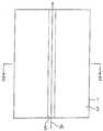
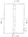
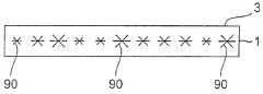
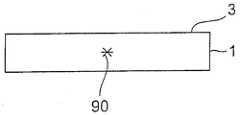
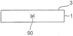
개질 영역은, 가공 대상물의 내부에 맞춘 레이저 광의 집광점에 대하여, 가공 대상물을 상대적으로 이동시킴으로써 형성된다. 그에 따르면, 상기 상대적 이동에 의해, 가공 대상물의 표면상의 절단 예정 라인에 따라 가공 대상물의 내부에 개질 영역을 형성하고 있다.The modified region is formed by relatively moving the object to be processed with respect to the light-converging point of laser light aligned with the inside of the object to be processed. According to this, the modified region is formed inside the object to be processed along the line along which the object is intended to be cut on the surface of the object by the relative movement.
개질 영역을 형성하는 공정 후, 절단 예정 라인에 따라 가공 대상물을 절단하는 절단 공정을 구비하도록 하여도 좋다. 개질 영역 형성 공정에 있어서 가공 대상물을 절단할 수 없는 경우, 이 절단 공정에 의해 가공 대상물을 절단한다. 절단 공정은, 개질 영역을 기점으로 하여 가공 대상물을 분할하기 때문에, 비교적 작은 힘으로 가공 대상물을 절단할 수 있다. 그에 따라, 가공 대상물의 표면에 절단 예정 라인으로부터 벗어난 불필요한 균열을 발생시키지 않고 가공 대상물의 절단이 가능해진다.And a cutting step of cutting the object along the line along which the object is intended to be cut, after the step of forming the modified region. When the object to be processed can not be cut in the modified region forming step, the object is cut by this cutting step. In the cutting step, since the object to be processed is divided starting from the modified region, the object can be cut with a relatively small force. As a result, it becomes possible to cut the object to be processed without generating unnecessary cracks deviating from the line along which the object is intended to be cut on the surface of the object.
가공 대상물로서, 유리, 압전 재료 및 반도체 재료를 포함하는 부재가 예시된다. 또한, 가공 대상물로서는 조사된 레이저 광의 투과성을 갖는 부재가 있다. 또한, 이 레이저 가공방법은, 표면에 전자 디바이스 또는 전극 패턴이 형성되어 있는 가공 대상물에 적용할 수 있다. 전자 디바이스는 반도체 소자, 액정 등의 표시장치, 압전 소자 등을 의미한다.As the object to be processed, a member including glass, a piezoelectric material, and a semiconductor material is exemplified. In addition, as the object to be processed, there is a member having transparency of the irradiated laser beam. Further, this laser processing method can be applied to an object to be processed in which an electronic device or an electrode pattern is formed on the surface. The electronic device means a semiconductor device, a display device such as a liquid crystal, a piezoelectric device, or the like.
본 발명에 관계되는 레이저 가공방법은, 반도체 재료의 내부에 집광점을 맞추어, 집광점에서의 피크 파워 밀도가 1×10⁸(W/㎠) 이상이고 또한 펄스폭이 1㎲ 이하인 조건으로 레이저 광을 조사하여, 반도체 재료의 절단 예정 라인에 따라 반도체 재료의 내부에 개질 영역을 형성하는 공정을 구비하는 것을 특징으로 한다. 또한, 본 발명에 관계되는 레이저 가공방법은, 압전 재료의 내부에 집광점을 맞추어, 집광점에서의 피크 파워 밀도가 1×10⁸(W/㎠) 이상이고 또한 펄스폭이 1㎲ 이하인 조건으로 레이저 광을 조사하여, 압전 재료의 절단 예정 라인에 따라 압전 재료의 내부에 개질 영역을 형성하는 공정을 구비하는 것을 특징으로 한다. 이들의 레이저 가공방법에 의하면, 상기 본 발명에 관계되는 레이저 가공방법과 같은 이유에 의해, 가공 대상물의 표면에 용융이나 절단 예정 라인으로부터 벗어난 불필요한 균열을 발생시키지 않고, 레이저 절단 가공이 가능해진다.A laser processing method according to the present invention is a laser processing method in which a laser light is irradiated under a condition that a light-converging point is set in a semiconductor material and a peak power density at a light-converging point is 1 占 08 (W / And forming a modified region in the semiconductor material along the line along which the object is to be cut in the semiconductor material. The laser processing method according to the present invention is a laser machining method according to the present invention, in which a light-converging point is set in a piezoelectric material, and a laser power is set to a value of 1 x 10 < 8 > And a step of forming a modified region in the piezoelectric material along the line along which the piezoelectric material is to be divided by irradiating light. According to these laser processing methods, it is possible to perform laser cutting processing on the surface of the object to be processed without causing unnecessary cracks deviating from melting and the line along which the object is intended to be cut, for the same reasons as in the laser processing method according to the present invention.
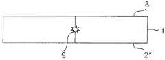
본 발명에 관계되는 레이저 가공방법에 있어서, 가공 대상물은, 그 표면에 복수의 회로부가 형성되어 있고, 복수의 회로부 중 인접하는 회로부 사이에 형성된 간극에 면하는 가공 대상물의 내부에 레이저 광의 집광점을 맞추도록 할 수 있다. 이것에 의하면, 인접하는 회로부 사이에 형성된 간극의 위치에 있어서, 가공 대상물을 확실하게 절단할 수 있다.In the laser processing method according to the present invention, the object to be processed is provided with a plurality of circuit portions on the surface thereof, and the light-converging point of the laser light is provided inside the object to be processed facing the gap formed between the adjacent circuit portions of the plurality of circuit portions You can make it fit. According to this, the object to be processed can be reliably cut at the position of the gap formed between the adjacent circuit portions.
본 발명에 관계되는 레이저 가공방법에 있어서, 복수의 회로부에 레이저 광이 조사되지 않는 각도로 레이저 광이 집광되도록 할 수 있다. 그에 따르면, 레이저 광이 회로부에 입사되는 것을 방지할 수 있어, 회로부를 레이저 광으로부터 보호할 수 있다.In the laser processing method according to the present invention, the laser light can be condensed at an angle at which the plurality of circuit portions are not irradiated with the laser light. According to this, laser light can be prevented from being incident on the circuit portion, and the circuit portion can be protected from the laser light.
본 발명에 관계되는 레이저 가공방법은, 반도체 재료의 내부에 집광점을 맞추어 레이저 광을 조사하여, 반도체 재료의 절단 예정 라인에 따라 반도체 재료의 내부에만 용융 처리 영역을 형성하는 공정을 구비하는 것을 특징으로 한다. 본 발명에 관계되는 레이저 가공방법에 의하면, 상기와 같은 이유에 의해 가공 대상물의 표면에 불필요한 균열을 발생시키지 않고 또한 그 표면이 용융하지 않고 레이저 가공이 가능해진다. 또, 용융 처리 영역의 형성은 다광자 흡수가 원인인 경우도 있고, 다른 원인인 경우도 있다.The laser machining method according to the present invention is characterized by including a step of irradiating laser light with a light-converging point inside a semiconductor material to form a molten processed region only in the semiconductor material along the line along which the semiconductor material is to be cut . According to the laser processing method of the present invention, unnecessary cracks are not generated on the surface of the object to be processed and laser processing can be performed without melting the surface due to the above reasons. In addition, the formation of the molten processed region may be due to multiphoton absorption or may be another cause.
(2) 본 발명에 관계되는 레이저 가공방법은, 1 이외의 타원율의 타원 편광을 한 레이저 광의 집광점을 가공 대상물의 내부에 맞추고 또한 레이저 광의 타원 편광을 나타내는 타원의 장축이 가공 대상물의 절단 예정 라인에 따르도록, 가공 대상물에 레이저 광을 조사함으로써, 절단 예정 라인에 따라 가공 대상물의 내부에 다광자 흡수에 의한 개질 영역을 형성하는 공정을 구비하는 것을 특징으로 한다.(2) In the laser processing method according to the present invention, the light-converging point of laser light having an elliptic polarization of ellipticity other than 1 is aligned with the inside of the object to be processed, and the long axis of the ellipse, And a step of forming a modified region by multiphoton absorption within the object to be processed along the line along which the object is intended to be cut by irradiating the object with laser light.
본 발명에 관계되는 레이저 가공방법에 의하면, 레이저 광의 타원 편광을 나타내는 타원의 장축이 가공 대상물의 절단 예정 라인에 따르도록, 가공 대상물에 레이저 광을 조사함으로써 개질 영역을 형성하고 있다. 본 발명자에 의하면, 타원 편광을 한 레이저 광을 사용하면, 타원 편광을 나타내는 타원의 장축 방향(즉, 편광의 기울기가 강한 방향)으로 개질 영역의 형성이 촉진되는 것을 알 수 있다. 따라서, 타원 편광을 나타내는 타원의 장축 방향이 가공 대상물의 절단 예정 라인에 따르도록, 레이저 광을 가공 대상물에 조사하여 개질 영역을 형성하면, 절단 예정 라인에 따른 개질 영역을 효율적으로 형성하는 것이 가능해진다. 따라서, 본 발명에 관계되는 레이저 가공방법에 의하면, 가공 대상물의 가공 스피드를 향상시킬 수 있다.According to the laser processing method of the present invention, the modified region is formed by irradiating the object with laser light so that the major axis of the ellipse representing the elliptically polarized light of the laser light follows the line along which the object is intended to be cut. According to the inventor of the present invention, the use of laser light having elliptically polarized light promotes the formation of the modified region in the major axis direction of the ellipse representing the elliptically polarized light (that is, the direction in which the slope of the polarized light is strong). Therefore, when the laser light is irradiated to the object to be processed so that the major axis direction of the ellipse representing the elliptical polarization follows the line along which the object is intended to be cut, it is possible to efficiently form the modified region along the line along which the object is intended to be cut . Therefore, according to the laser processing method of the present invention, the processing speed of the object to be processed can be improved.
또한, 본 발명에 관계되는 레이저 가공방법에 의하면, 절단 예정 라인에 따른 방향 이외에 있어서 개질 영역의 형성이 억제되기 때문에, 가공 대상물을 절단 예정 라인에 따라 정밀하게 절단하는 것이 가능해진다.Further, according to the laser processing method of the present invention, formation of the modified region is suppressed in a direction other than along the line along which the object is intended to be cut, so that it becomes possible to precisely cut the object along the line along which the object is intended to be cut.
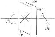
여기서, 타원율은 타원의 단축의 길이의 반/장축의 길이의 반이다. 레이저 광의 타원율이 작을수록, 개질 영역은 절단 예정 라인에 따른 방향의 형성이 촉진되고 또한 그 이외의 방향의 형성이 억제된다. 타원율은 가공 대상물의 두께나 재질 등을 고려하여 결정할 수 있다. 직선 편광은 타원율이 영인 타원 편광이다.Here, the ellipticity is half the length of the short axis of the ellipse / half of the long axis. The smaller the ellipticity of the laser light, the more the formation of the direction along the line along which the material is to be divided is promoted and the formation of the other direction is suppressed. The ellipticity can be determined in consideration of the thickness and material of the object to be processed. Linearly polarized light is elliptic polarized light whose ellipticity is zero.
본 발명에 관계되는 레이저 가공방법은, 1 이외의 타원율의 타원 편광을 한 레이저 광의 집광점을 가공 대상물의 내부에 맞추고 또한 레이저 광의 타원 편광을 나타내는 타원의 장축이 가공 대상물의 절단 예정 라인에 따르도록, 집광점에서의 피크 파워 밀도가 1×10⁸(W/㎠) 이상이고 또한 펄스폭이 1㎲ 이하인 조건으로 레이저 광을 조사함으로써, 절단 예정 라인에 따라 가공 대상물의 내부에 크랙 영역을 포함하는 개질 영역을 형성하는 공정을 구비하는 것을 특징으로 한다.A laser processing method according to the present invention is a laser processing method in which a light converging point of an elliptically polarized elliptical polarized laser beam other than 1 is aligned with the inside of an object to be processed and a long axis of an ellipse showing elliptical polarization of the laser light follows a line along which a object is intended to be cut , The laser light is irradiated under the condition that the peak power density at the light-converging point is 1 占 08 (W / cm2) or more and the pulse width is 1 占 퐏 or less, And a step of forming a region.
본 발명에 관계되는 레이저 가공방법에 의하면, 레이저 광의 타원 편광을 나타내는 타원의 장축이 가공 대상물의 절단 예정 라인에 따르도록 가공 대상물에 레이저 광을 조사하고 있기 때문에, 상기 본 발명에 관계되는 레이저 가공방법과 같이, 개질 영역을 효율적으로 형성할 수 있고, 또한, 절단 예정 라인에 따라 가공 대상물을 정밀하게 절단할 수 있다.According to the laser processing method of the present invention, laser light is irradiated on the object to be processed so that the major axis of the ellipse representing the elliptically polarized light of the laser light follows the line along which the object is intended to be cut. The modified region can be efficiently formed and the object to be processed can be precisely cut along the line along which the object is intended to be cut.
본 발명에 관계되는 레이저 가공방법은, 1 이외의 타원율의 타원 편광을 한 레이저 광의 집광점을 가공 대상물의 내부에 맞추고 또한 레이저 광의 타원 편광을 나타내는 타원의 장축이 가공 대상물의 절단 예정 라인에 따르도록, 집광점에서의 피크 파워 밀도가 1×10⁸(W/㎠) 이상이고 또한 펄스폭이 1㎲ 이하인 조건으로 레이저 광을 조사함으로써, 절단 예정 라인에 따라 가공 대상물의 내부에 용융 처리 영역을 포함하는 개질 영역을 형성하는 공정을 구비하는 것을 특징으로 한다.A laser processing method according to the present invention is a laser processing method in which a light converging point of an elliptically polarized elliptical polarized laser beam other than 1 is aligned with the inside of an object to be processed and a long axis of an ellipse showing elliptical polarization of the laser light follows a line along which a object is intended to be cut , The laser light is irradiated under the condition that the peak power density at the light-converging point is not less than 1 占 08 (W / cm2) and the pulse width is not more than 1 占 퐏, And a step of forming a modified region.
본 발명에 관계되는 레이저 가공방법에 의하면, 레이저 광의 타원 편광을 나타내는 타원의 장축이 가공 대상물의 절단 예정 라인에 따르도록 가공 대상물에 레이저 광을 조사하고 있기 때문에, 상기 본 발명에 관계되는 레이저 가공방법과 같이, 개질 영역을 효율적으로 형성할 수 있고, 또한, 절단 예정 라인에 따라 가공 대상물을 정밀하게 절단할 수 있다.According to the laser processing method of the present invention, laser light is irradiated on the object to be processed so that the major axis of the ellipse representing the elliptically polarized light of the laser light follows the line along which the object is intended to be cut. The modified region can be efficiently formed and the object to be processed can be precisely cut along the line along which the object is intended to be cut.
본 발명에 관계되는 레이저 가공방법은, 1 이외의 타원율의 타원 편광을 한 레이저 광의 집광점을 가공 대상물의 내부에 맞추고 또한 레이저 광의 타원 편광을 나타내는 타원의 장축이 가공 대상물의 절단 예정 라인에 따르도록, 집광점에서의 피크 파워 밀도가 1×10⁸(W/㎠) 이상이고 또한 펄스폭이 1ns 이하인 조건으로 레이저 광을 조사함으로써, 절단 예정 라인에 따라 가공 대상물의 내부에 굴절율이 변화된 영역인 굴절율 변화 영역을 포함하는 개질 영역을 형성하는 공정을 구비하는 것을 특징으로 한다.A laser processing method according to the present invention is a laser processing method in which a light converging point of an elliptically polarized elliptical polarized laser beam other than 1 is aligned with the inside of an object to be processed and a long axis of an ellipse showing elliptical polarization of the laser light follows a line along which a object is intended to be cut , The laser light is irradiated under the condition that the peak power density at the light-converging point is 1 占 08 (W / cm2) or more and the pulse width is 1 ns or less to change the refractive index in the region of the object to be processed, And a step of forming a modified region including a region.
본 발명에 관계되는 레이저 가공방법에 의하면, 레이저 광의 타원 편광을 나타내는 타원의 장축이 가공 대상물의 절단 예정 라인에 따르도록 가공 대상물에 레이저 광을 조사하고 있기 때문에, 상기 본 발명에 관계되는 레이저 가공방법과 같이, 개질 영역을 효율적으로 형성할 수 있고, 또한, 절단 예정 라인에 따라 가공 대상물을 정밀하게 절단할 수 있다.According to the laser processing method of the present invention, laser light is irradiated on the object to be processed so that the major axis of the ellipse representing the elliptically polarized light of the laser light follows the line along which the object is intended to be cut. The modified region can be efficiently formed and the object to be processed can be precisely cut along the line along which the object is intended to be cut.
상기 본 발명에 관계되는 레이저 가공방법에 적용할 수 있는 예는 이하와 같다.Examples that can be applied to the laser processing method according to the present invention are as follows.
타원율이 영인 타원 편광을 갖는 레이저 광을 사용할 수 있다. 타원율이 영인 경우, 직선 편광이 된다. 직선 편광에 의하면, 개질 영역의 절단 예정 라인에 따른 방향의 치수를 최대한으로 하면서 또한 그 이외의 방향의 치수를 최소한으로 하는 것이 가능해진다. 또한, 타원 편광의 타원율을 1/4 파장판 방위각 변화에 의해 조절할 수 있다. 1/4 파장판을 사용하면, 방위각을 변화시키는 것만으로 타원율을 조절할 수 있다.A laser beam having an elliptically polarized light whose ellipticity is zero can be used. When the ellipticity is zero, it becomes linearly polarized light. According to the linearly polarized light, the dimension in the direction along the line along which the object is intended to be cut in the modified region can be maximized while the dimensions in the other directions can be minimized. In addition, the ellipticity of the elliptically polarized light can be adjusted by changing the azimuth angle of the quarter wave plate. If a quarter wave plate is used, the ellipticity can be adjusted only by changing the azimuth angle.
개질 영역을 형성하는 공정 후, 1/2 파장판에 의해 레이저 광의 편광을 약 90°만큼 회전시켜, 가공 대상물에 레이저 광을 조사할 수 있다. 또한, 개질 영역을 형성하는 공정 후, 가공 대상물의 두께 방향을 축으로 하여, 가공 대상물을 약 90°만큼 회전시켜, 가공 대상물에 레이저 광을 조사할 수 있다. 그에 따라, 가공 대상물의 표면에 따른 방향으로 연장되고 또한 개질 영역과 교차한 다른 개질 영역을 가공 대상물의 내부에 형성할 수 있다. 따라서, 예를 들면, X축 방향 및 Y축 방향의 절단 예정 라인에 따른 개질 영역을 효율적으로 형성할 수 있다.After the process of forming the modified region, the polarization of the laser light is rotated by about 90 DEG by the 1/2 wavelength plate, and the object to be processed can be irradiated with laser light. Further, after the step of forming the modified region, the object to be processed may be rotated by about 90 degrees about the thickness direction of the object to be processed, thereby irradiating the object with laser light. Thereby, another modified region extending in the direction along the surface of the object to be processed and crossing the modified region can be formed inside the object to be processed. Therefore, for example, the modified regions along the lines along which the object is intended to be cut in the X-axis direction and the Y-axis direction can be efficiently formed.
본 발명에 관계되는 레이저 가공방법은, 1 이외의 타원율의 타원 편광을 한 레이저 광의 집광점을 가공 대상물의 내부에 맞추고 또한 레이저 광의 타원 편광을 나타내는 타원의 장축이 가공 대상물의 절단 예정 라인에 따르도록 하여, 가공 대상물에 레이저 광을 조사함으로써, 절단 예정 라인에 따라 가공 대상물을 절단하는 공정을 구비하는 것을 특징으로 한다.A laser processing method according to the present invention is a laser processing method in which a light converging point of an elliptically polarized elliptical polarized laser beam other than 1 is aligned with the inside of an object to be processed and a long axis of an ellipse showing elliptical polarization of the laser light follows a line along which a object is intended to be cut And cutting the object along the line along which the object is intended to be cut by irradiating the object with laser light.
본 발명에 관계되는 레이저 가공방법에 의하면, 레이저 광의 타원 편광을 나타내는 타원의 장축이 가공 대상물의 절단 예정 라인에 따르도록, 가공 대상물의 내부에 집광점을 맞추어 가공 대상물에 레이저 광을 조사하고 있다. 따라서, 가공 대상물을 절단 예정 라인에 따라 효율적으로 절단하는 것이 가능해진다. 본 발명에 관계되는 레이저 가공방법은, 가공 대상물에 레이저 광을 흡수시키고, 가공 대상물을 가열 용융시킴으로써, 가공 대상물을 절단하여도 좋다. 또한, 본 발명에 관계되는 레이저 가공방법은, 가공 대상물에 레이저 광을 조사함으로써 다광자 흡수를 발생시키고, 그에 따라 가공 대상물의 내부에 개질 영역을 형성하고, 개질 영역을 기점으로 하여 가공 대상물을 절단하여도 좋다.According to the laser processing method of the present invention, laser light is irradiated on an object to be processed by aligning the light-converging point inside the object so that the major axis of the ellipse representing the elliptical polarization of the laser light follows the line along which the object is to be cut. Therefore, it becomes possible to efficiently cut the object to be processed along the line along which the object is intended to be cut. In the laser processing method according to the present invention, the object to be processed may be cut by absorbing laser light to the object to be processed and heating and melting the object to be processed. Further, a laser processing method according to the present invention is a laser processing method according to the present invention for generating a multiphoton absorption by irradiating a laser beam to an object to be processed, thereby forming a modified region inside the object and cutting the object .
본 발명에 관계되는 레이저 가공장치는 펄스폭이 1㎲ 이하인 펄스 레이저 광을 출사하는 레이저 광원과, 레이저 광원으로부터 출사된 펄스 레이저 광을 1 이외의 타원율의 타원 편광으로 조절하는 타원율 조절 수단과, 타원율 조절 수단에 의해 조절된 펄스 레이저 광의 타원 편광을 나타내는 타원의 장축이 가공 대상물의 절단 예정 라인에 따르도록 조절하는 장축 조절 수단과, 장축 조절 수단에 의해 조절된 펄스 레이저 광의 집광점의 피크 파워 밀도가 1×10⁸(W/㎠) 이상이 되도록 펄스 레이저 광을 집광하는 집광 수단과, 집광 수단에 의해 집광된 펄스 레이저 광의 집광점을 가공 대상물의 내부에 맞추는 수단과, 절단 예정 라인에 따라 펄스 레이저 광의 집광점을 상대적으로 이동시키는 이동 수단을 구비하는 것을 특징으로 한다.The laser processing apparatus according to the present invention comprises a laser light source for emitting pulsed laser light having a pulse width of 1 μs or less, ellipticity adjusting means for adjusting the pulse laser light emitted from the laser light source to an elliptic polarized light other than 1, A long axis adjusting means for adjusting the long axis of the ellipse representing the elliptically polarized light of the pulsed laser light controlled by the adjusting means so as to follow the line along which the object is intended to be cut in the object to be processed; Converging means for converging the pulsed laser light so as to be at least 1 x 10 8 (W / cm 2); means for aligning the light-converging point of the pulsed laser light condensed by the condensing means inside the object to be processed; And a moving means for relatively moving the light-converging point.
본 발명에 관계되는 레이저 가공장치에 의하면, 상기 본 발명에 관계되는 레이저 가공방법과 같은 이유에 의해, 가공 대상물의 표면에 용융이나 절단 예정 라인으로부터 벗어난 불필요한 균열을 발생시키지 않고, 레이저 절단 가공이 가능해진다. 또한, 레이저 광의 타원 편광을 나타내는 타원의 장축이 가공 대상물의 절단 예정 라인에 따르도록 가공 대상물에 레이저 광을 조사하고 있기 때문에, 상기 본 발명에 관계되는 레이저 가공방법과 같이, 개질 영역을 효율적으로 형성할 수 있고, 또한, 절단 예정 라인에 따라 가공 대상물을 정밀하게 절단할 수 있다.According to the laser machining apparatus of the present invention, it is possible to perform laser cutting processing on the surface of an object to be processed without generating unnecessary cracks deviating from melting and the line along which the object is intended to be cut due to the same reason as the above- It becomes. Further, since the laser light is irradiated on the object to be processed so that the major axis of the ellipse representing the elliptically polarized light of the laser light follows the line along which the object is intended to be cut in the object to be processed, as in the laser processing method according to the present invention, And the object to be processed can be precisely cut along the line along which the object is intended to be cut.
상기 본 발명에 관계되는 레이저 가공장치에 적용할 수 있는 예는 이하와 같다.Examples that can be applied to the laser processing apparatus according to the present invention are as follows.
타원율 조절 수단에 의해 조절된 펄스 레이저 광의 편광을 약 90°만큼 회전 조절하는 90° 회전 조절 수단을 구비하도록 할 수 있다. 또한, 가공 대상물의 두께 방향을 축으로 하여 가공 대상물이 배치되는 배치대를 약 90°만큼 회전시키는 회전 수단을 구비하도록 할 수 있다. 그에 따라, 펄스 레이저 광의 타원 편광을 나타내는 타원의 장축을 가공 대상물의 표면에 따른 방향으로 연장되고 또한 절단 예정 라인과 교차하는 방향으로 연장되는 다른 절단 예정 라인에 따르도록 할 수 있다. 따라서, 예를 들면, X축 방향 및 Y축 방향의 절단 예정 라인에 따른 개질 영역을 효율적으로 형성할 수 있다.And 90 DEG rotation adjusting means for adjusting the polarization of the pulsed laser light adjusted by the ellipticity adjusting means by about 90 DEG. Further, it may be provided with a rotating means for rotating the placing table on which the object to be processed is disposed, about the axis of the object in the thickness direction, by about 90 degrees. Accordingly, the major axis of the ellipse representing the elliptically polarized light of the pulsed laser light can be made to follow another line along which the object is intended to be cut extending in the direction along the surface of the object to be processed and extending in the direction intersecting the line along which the object is intended to be cut. Therefore, for example, the modified regions along the lines along which the object is intended to be cut in the X-axis direction and the Y-axis direction can be efficiently formed.
본 발명에 관계되는 레이저 가공장치는 펄스폭이 1㎲ 이하이고 또한 직선 편광을 갖는 펄스 레이저 광을 출사하는 레이저 광원과, 레이저 광원으로부터 출사된 펄스 레이저 광의 직선 편광의 방향이 가공 대상물의 절단 예정 라인에 따르도록 조절하는 직선 편광 조절 수단과, 직선 편광 조절 수단에 의해 조절된 펄스 레이저 광의 집광점의 피크 파워 밀도가 1×10⁸(W/㎠) 이상이 되도록 펄스 레이저 광을 집광하는 집광 수단과, 집광 수단에 의해 집광된 펄스 레이저 광의 집광점을 가공 대상물의 내부에 맞추는 수단과, 절단 예정 라인에 따라 펄스 레이저 광의 집광점을 상대적으로 이동시키는 이동 수단을 구비하는 것을 특징으로 한다.A laser machining apparatus according to the present invention is characterized in that a laser light source for emitting a pulsed laser light having a pulse width of 1 占 퐏 or less and having a linearly polarized light and a linearly polarized light source for emitting a pulse laser light, Converging means for converging the pulsed laser light so that the peak power density of the light-converging point of the pulsed laser light adjusted by the linearly polarizing light adjusting means is not less than 1 占 08 (W / cm2); and A means for adjusting the light-converging point of the pulsed laser light focused by the light-converging means inside the object to be processed; and a moving means for relatively moving the light-converging point of the pulse laser light along the line along which the object is intended to be cut.
본 발명에 관계되는 레이저 가공장치에 의하면, 상기 본 발명에 관계되는 레이저 가공방법과 같은 이유에 의해, 가공 대상물의 표면에 용융이나 절단 예정 라인으로부터 벗어난 불필요한 균열을 발생시키지 않고, 레이저 절단 가공이 가능해진다. 또한, 본 발명에 관계되는 레이저 가공장치에 의하면, 상기 본 발명에 관계되는 레이저 가공방법과 같이, 개질 영역을 효율적으로 형성할 수 있고, 또한, 절단 예정 라인에 따라 가공 대상물을 정밀하게 절단할 수 있다.According to the laser machining apparatus of the present invention, it is possible to perform laser cutting processing on the surface of an object to be processed without generating unnecessary cracks deviating from melting and the line along which the object is intended to be cut due to the same reason as the above- It becomes. Further, according to the laser machining apparatus of the present invention, as in the laser machining method according to the present invention, it is possible to efficiently form the modified region and to cut the object precisely along the line along which the object is intended to be cut have.
(3) 본 발명에 관계되는 레이저 가공장치는 펄스폭이 1㎲ 이하인 펄스 레이저 광을 출사하는 레이저 광원과, 펄스 레이저 광의 파워 크기의 입력에 근거하여 레이저 광원으로부터 출사되는 펄스 레이저 광의 파워의 크기를 조절하는 파워 조절 수단과, 레이저 광원으로부터 출사된 펄스 레이저 광의 집광점의 피크 파워 밀도가 1×10⁸(W/㎠) 이상이 되도록 펄스 레이저 광을 집광하는 집광 수단과, 집광 수단에 의해 집광된 펄스 레이저 광의 집광점을 가공 대상물의 내부에 맞추는 수단과, 가공 대상물의 절단 예정 라인에 따른 펄스 레이저 광의 집광점을 상대적으로 이동시키는 이동 수단을 구비하고, 가공 대상물의 내부에 집광점을 맞추어 1펄스의 펄스 레이저 광을 가공 대상물에 조사함으로써 가공 대상물의 내부에 1개의 개질 스폿(spot)이 형성되고, 파워 조절 수단에 의해 조절되는 펄스 레이저 광의 파워의 크기와 개질 스폿의 치수의 상관관계를 미리 기억한 상관관계 기억 수단과, 입력된 펄스 레이저 광의 파워의 크기에 근거하여 이 크기의 파워로 형성되는 개질 스폿의 치수를 상관관계 기억 수단으로부터 선택하는 치수 선택 수단과, 치수 선택 수단에 의해 선택된 개질 스폿의 치수를 표시하는 치수 표시 수단을 구비하는 것을 특징으로 한다.(3) A laser processing apparatus according to the present invention is characterized by comprising: a laser light source for emitting a pulsed laser beam having a pulse width of 1 μs or less; and a pulse laser light source for outputting pulsed laser light, A condensing means for condensing the pulsed laser light so that the peak power density of the light-converging point of the pulsed laser light emitted from the laser light source is not less than 1 x 10 8 (W / cm 2); and a pulse condensed by the condensing means And a moving means for relatively moving the light-converging point of the pulsed laser light along the line along which the object is intended to be cut in the object to be processed. The light-converging point is set in the object to be processed, One modified spot is formed inside the object by irradiating the object with pulse laser light, A correlation storage means for previously storing a correlation between the magnitude of the power of the pulsed laser light controlled by the adjustment means and the dimension of the modified spot, and a correlation storage means for storing, based on the magnitude of the power of the inputted pulse laser light, And a dimension display means for displaying the dimension of the modified spot selected by the dimension selection means.
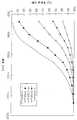
본 발명자에 의하면, 펄스 레이저 광의 파워를 작게 하면 개질 스폿이 작아지도록 제어할 수 있고, 펄스 레이저 광의 파워를 크게 하면 개질 스폿이 커지도록 제어할 수 있는 것을 알 수 있다. 개질 스폿은, 1펄스의 펄스 레이저 광에 의해 형성되는 개질 부분이고, 개질 스폿이 모임으로써 개질 영역이 된다. 개질 스폿의 치수의 제어는 가공 대상물의 절단에 영향을 미친다. 즉, 개질 스폿이 지나치게 크면, 가공 대상물의 절단 예정 라인에 따른 절단의 정밀도 및 절단면의 평탄성이 나빠진다. 한편, 두께가 큰 가공 대상물에 대하여 개질 스폿이 극단적으로 지나치게 작으면 가공 대상물의 절단이 곤란해진다. 본 발명에 관계되는 레이저 가공장치에 의하면, 펄스 레이저 광의 파워의 크기를 조절함으로써, 개질 스폿의 치수를 제어할 수 있다. 이 때문에, 절단 예정 라인에 따라 정밀하게 가공 대상물을 절단할 수 있고, 또한 평탄한 절단면을 얻을 수 있다.According to the inventor of the present invention, it is possible to control the modified spot to be small by reducing the power of the pulse laser light, and to control the modified spot to be large by increasing the power of the pulse laser light. The modified spot is a modified portion formed by one pulse of pulsed laser light, and the modified spot is a modified region. Control of the dimension of the modified spot affects the cutting of the object to be processed. In other words, if the modified spot is too large, the precision of cutting along the line along which the object is intended to be cut and the flatness of the cut surface of the object to be processed deteriorate. On the other hand, if the modified spot is extremely excessively small relative to the object to be processed having a large thickness, it becomes difficult to cut the object. According to the laser machining apparatus of the present invention, the dimension of the modified spot can be controlled by adjusting the magnitude of the power of the pulsed laser light. Therefore, the object to be processed can be precisely cut along the line along which the object is intended to be cut, and a flat cut surface can be obtained.
또한, 본 발명에 관계되는 레이저 가공장치는 펄스 레이저 광의 파워의 크기와 개질 스폿의 치수의 상관관계를 미리 기억한 상관관계 기억 수단을 구비한다. 입력된 펄스 레이저 광의 파워의 크기에 근거하여 이 크기의 파워로 형성되는 개질 스폿의 치수를 상관관계 기억 수단으로부터 선택하고, 선택된 개질 스폿의 치수를 표시하고 있다. 따라서, 레이저 가공장치에 입력된 펄스 레이저 광의 파워의 크기에 의해 형성되는 개질 스폿의 치수를 레이저 가공 전에 알 수 있다.Further, the laser processing apparatus according to the present invention includes correlation storage means for previously storing the correlation between the magnitude of the power of the pulsed laser light and the dimension of the modified spot. The dimension of the modified spot formed by the power of this size is selected from the correlation storage means based on the magnitude of the power of the input pulsed laser light and the dimension of the selected modified spot is displayed. Therefore, the dimension of the modified spot formed by the magnitude of the power of the pulsed laser light input to the laser processing apparatus can be known before laser processing.
본 발명에 관계되는 레이저 가공장치는 펄스폭이 1㎲ 이하인 펄스 레이저 광을 출사하는 레이저 광원과, 레이저 광원으로부터 출사된 펄스 레이저 광의 집광점의 피크 파워 밀도가 1×10⁸(W/㎠) 이상이 되도록 펄스 레이저 광을 집광하는 집광용 렌즈와, 개구수의 크기의 입력에 근거하여 집광용 렌즈를 포함하는 광학계의 개구수의 크기를 조절하는 개구수 조절 수단과, 집광용 렌즈에 의해 집광된 펄스 레이저 광의 집광점을 가공 대상물의 내부에 맞추는 수단과, 가공 대상물의 절단 예정 라인에 따라 펄스 레이저 광의 집광점을 상대적으로 이동시키는 이동 수단을 구비하고, 가공 대상물의 내부에 집광점을 맞추어 1펄스의 펄스 레이저 광을 가공 대상물에 조사함으로써 가공 대상물의 내부에 1개의 개질 스폿이 형성되고, 개구수 조절 수단에 의해 조절되는 개구수의 크기와 개질 스폿의 치수의 상관관계를 미리 기억한 상관관계 기억 수단과, 입력된 개구수의 크기에 근거하여 이 크기의 개구수로 형성되는 개질 스폿의 치수를 상관관계 기억 수단으로부터 선택하는 치수 선택 수단과, 치수 선택 수단에 의해 선택된 개질 스폿의 치수를 표시하는 치수 표시 수단을 구비하는 것을 특징으로 한다.The laser processing apparatus according to the present invention is characterized in that the laser light source for emitting a pulsed laser beam having a pulse width of 1 占 퐏 or less and the laser light source for outputting pulsed laser light having a peak power density of not less than 1 占 08 (W / A numerical aperture adjusting means for adjusting the numerical aperture of the optical system including the light-converging lens on the basis of the input of the numerical aperture size, and a condensing lens for condensing the pulse condensed by the condensing lens And a moving means for moving the light-converging point of the pulsed laser light relatively along the line along which the object is intended to be cut in the object to be processed. The light-converging point is set in the object to be processed, One modified spot is formed inside the object to be processed by irradiating the object with the pulsed laser light, and adjusted by the numerical aperture adjusting means Correlation storage means for previously storing the correlation between the magnitude of the numerical aperture and the dimension of the modified spot, and a correlation storage means for storing the dimension of the modified spot formed by the numerical aperture of this size on the basis of the inputted numerical aperture size And a dimension display means for displaying the dimension of the modified spot selected by the dimension selection means.
본 발명자에 의하면, 집광용 렌즈를 포함하는 광학계의 개구수를 크게 하면 개질 스폿을 작게 제어할 수 있고, 그 개구수를 작게 하면 개질 스폿을 크게 제어할 수 있는 것을 알 수 있다. 따라서, 본 발명에 관계되는 레이저 가공장치에 의하면, 집광용 렌즈를 포함하는 광학계의 개구수의 크기를 조절함으로써 개질 스폿의 치수를 제어할 수 있다.According to the present inventor, it can be seen that the modified spot can be controlled to be small by increasing the numerical aperture of the optical system including the light-converging lens, and the modified spot can be controlled largely by reducing the numerical aperture. Therefore, according to the laser machining apparatus of the present invention, the dimension of the modified spot can be controlled by adjusting the numerical aperture of the optical system including the light-converging lens.
또한, 본 발명에 관계되는 레이저 가공장치는 개구수의 크기와 개질 스폿의 치수의 상관관계를 미리 기억한 상관관계 기억 수단을 구비한다. 입력된 개구수의 크기에 근거하여 이 크기의 개구수로 형성되는 개질 스폿의 치수를 상관관계 기억 수단으로부터 선택하고, 선택된 개질 스폿의 치수를 표시하고 있다. 따라서, 레이저 가공장치에 입력된 개구수의 크기에 의해 형성되는 개질 스폿의 치수를 레이저 가공 전에 알 수 있다.Further, the laser machining apparatus according to the present invention includes correlation storage means for previously storing the correlation between the size of the numerical aperture and the dimension of the modified spot. The dimension of the modified spot formed by the numerical aperture of this size is selected from the correlation storage means based on the magnitude of the inputted numerical aperture and the dimension of the selected modified spot is displayed. Therefore, the dimension of the modified spot formed by the size of the numerical aperture inputted to the laser processing apparatus can be known before laser processing.
본 발명에 관계되는 레이저 가공장치는 펄스폭이 1㎲ 이하인 펄스 레이저 광을 출사하는 레이저 광원과, 레이저 광원으로부터 출사된 펄스 레이저 광의 집광점의 피크 파워 밀도가 1×10⁸(W/㎠) 이상이 되도록 펄스 레이저 광을 집광하는 집광용 렌즈를 복수 포함하고 또한 복수의 집광용 렌즈를 선택 가능한 렌즈 선택 수단을 구비하고, 복수의 집광용 렌즈를 포함하는 광학계는 각각 개구수가 다르고, 렌즈 선택 수단으로 선택된 집광용 렌즈에 의해 집광된 펄스 레이저 광의 집광점을 가공 대상물의 내부에 맞추는 수단과, 가공 대상물의 절단 예정 라인에 따라 펄스 레이저 광의 집광점을 상대적으로 이동시키는 이동 수단을 구비하고, 가공 대상물의 내부에 집광점을 맞추어 1펄스의 펄스 레이저 광을 가공 대상물에 조사함으로써 가공 대상물의 내부에 1개의 개질 스폿이 형성되고, 복수의 집광용 렌즈를 포함하는 광학계의 개구수의 크기와 개질 스폿의 치수의 상관관계를 미리 기억한 상관관계 기억 수단과, 선택된 집광용 렌즈를 포함하는 광학계의 개구수의 크기에 근거하여 이 크기의 개구수로 형성되는 개질 스폿의 치수를 상관관계 기억 수단으로부터 선택하는 치수 선택 수단과, 치수 선택 수단에 의해 선택된 개질 스폿의 치수법을 표시하는 치수 표시 수단을 구비하는 것을 특징으로 한다.The laser processing apparatus according to the present invention is characterized in that the laser light source for emitting a pulsed laser beam having a pulse width of 1 占 퐏 or less and the laser light source for outputting pulsed laser light having a peak power density of not less than 1 占 08 (W / And a plurality of light-converging lenses, wherein the optical system including the plurality of light-converging lenses has a different numerical aperture and is selected as the lens selecting means A means for adjusting the light-converging point of the pulsed laser light focused by the light-converging lens to the inside of the object to be processed; and a moving means for relatively moving the light-converging point of the pulse laser light along the line along which the object is to be cut, And a pulsed laser beam of one pulse is irradiated to the object to be processed, whereby 1 Correlation storing means for previously storing a correlation between the size of the numerical aperture of the optical system including the plurality of light-converging lenses and the dimension of the modified spot, and the numerical aperture of the optical system including the selected condensing lens And a dimension display means for displaying a dimension method of the modified spot selected by the dimension selection means, wherein the size of the modified spot is determined based on the size of the modified spot, .
본 발명에 관계되는 레이저 가공장치에 의하면, 개질 스폿의 치수를 제어할 수 있다. 또한, 선택된 집광용 렌즈를 포함하는 광학계의 개구수의 크기에 의해 형성되는 개질 스폿의 치수를 레이저 가공 전에 알 수 있다.According to the laser machining apparatus of the present invention, the dimension of the modified spot can be controlled. Further, the dimension of the modified spot formed by the numerical aperture of the optical system including the selected light-converging lens can be known before laser processing.
본 발명에 관계되는 레이저 가공장치는 펄스폭이 1㎲ 이하인 펄스 레이저 광을 출사하는 레이저 광원과, 펄스 레이저 광의 파워 크기의 입력에 근거하여 레이저 광원으로부터 출사되는 펄스 레이저 광의 파워의 크기를 조절하는 파워 조절 수단과, 레이저 광원으로부터 출사된 펄스 레이저 광의 집광점의 피크 파워 밀도가 1×10⁸(W/㎠) 이상이 되도록 펄스 레이저 광을 집광하는 집광용 렌즈와, 개구수의 크기의 입력에 근거하여 집광용 렌즈를 포함하는 광학계의 개구수의 크기를 조절하는 개구수 조절 수단과, 집광용 렌즈에 의해 집광된 펄스 레이저 광의 집광점을 가공 대상물의 내부에 맞추는 수단과, 가공 대상물의 절단 예정 라인에 따라 펄스 레이저 광의 집광점을 상대적으로 이동시키는 이동 수단을 구비하고, 가공 대상물의 내부에 집광점을 맞추어 1펄스의 펄스 레이저 광을 가공 대상물에 조사함으로써 가공 대상물의 내부에 1개의 개질 스폿이 형성되고, 파워 조절 수단에 의해 조절되는 펄스 레이저 광의 파워의 크기 및 개구수 조절 수단에 의해 조절되는 개구수의 크기의 세트와 개질 스폿의 치수의 상관관계를 미리 기억한 상관관계 기억 수단과, 입력된 펄스 레이저 광의 파워의 크기에 및 입력된 개구수의 크기에 근거하여 이들의 크기로 형성되는 개질 스폿의 치수를 상관관계 기억 수단으로부터 선택하는 치수 선택 수단과, 치수 선택 수단에 의해 선택된 개질 스폿의 치수를 표시하는 치수 표시 수단을 구비하는 것을 특징으로 한다.A laser processing apparatus according to the present invention includes a laser light source for emitting a pulsed laser beam having a pulse width of 1 μs or less and a power adjusting unit for adjusting the power of pulsed laser light emitted from the laser light source based on input of the power magnitude of the pulsed laser light And a condensing lens for condensing the pulsed laser light so that the peak power density of the light-converging point of the pulsed laser light emitted from the laser light source is not less than 1 x 10 8 (W / cm 2) A numerical aperture adjusting means for adjusting the numerical aperture of the optical system including the light-converging lens, means for adjusting the light-converging point of the pulsed laser light condensed by the light-converging lens to the inside of the object to be processed, And a moving means for relatively moving the light-converging point of the pulsed laser light, wherein a light-converging point is set inside the object to be processed One modified spot is formed inside the object by irradiating the object with pulsed laser light of one pulse and the magnitude of the power of the pulsed laser light controlled by the power adjusting means and the numerical aperture A correlation storage means for previously storing a correlation between the size of the modified pulse laser beam and the dimension of the modified spot and a correlation storage means for storing a correlation between the magnitude of the power of the inputted pulse laser beam and the magnitude of the inputted numerical aperture, Dimensional selection means for selecting a dimension from the correlation storage means and a dimension display means for displaying the dimension of the modified spot selected by the dimension selection means.
본 발명에 관계되는 레이저 가공장치에 의하면, 파워의 조절과 개구수의 조절을 조합할 수 있기 때문에, 개질 스폿의 치수를 제어할 수 있는 크기의 종류를 증가시키는 것이 가능해진다. 또한, 상기 본 발명에 관계되는 레이저 가공장치와 같은 이유에 의해, 개질 스폿의 치수를 레이저 가공 전에 알 수 있다.According to the laser machining apparatus of the present invention, since it is possible to combine the adjustment of the power and the numerical aperture, it becomes possible to increase the number of kinds of magnets capable of controlling the dimension of the modified spot. Further, for the same reasons as those of the laser machining apparatus according to the present invention, the dimensions of the modified spot can be known before laser processing.
본 발명에 관계되는 레이저 가공장치는 펄스폭이 1㎲ 이하인 펄스 레이저 광을 출사하는 레이저 광원과, 펄스 레이저 광의 파워 크기의 입력에 근거하여 레이저 광원으로부터 출사되는 펄스 레이저 광의 파워의 크기를 조절하는 파워 조절 수단과, 레이저 광원으로부터 출사된 펄스 레이저 광의 집광점의 피크 파워 밀도가 1×10⁸(W/㎠) 이상이 되도록 펄스 레이저 광을 집광하는 집광용 렌즈를 복수 포함하고 또한 복수의 집광용 렌즈를 선택 가능한 렌즈 선택 수단을 구비하고, 복수의 집광용 렌즈를 포함하는 광학계는 각각 개구수가 다르고, 렌즈 선택 수단으로 선택된 집광용 렌즈에 의해 집광된 펄스 레이저 광의 집광점을 가공 대상물의 내부에 맞추는 수단과, 가공 대상물의 절단 예정 라인에 따라 펄스 레이저 광의 집광점을 상대적으로 이동시키는 이동 수단을 구비하고, 가공 대상물의 내부에 집광점을 맞추어 1펄스의 펄스 레이저 광을 가공 대상물에 조사함으로써, 가공 대상물의 내부에 1개의 개질 스폿이 형성되고, 파워 조절 수단에 의해 조절되는 펄스 레이저 광의 파워의 크기 및 복수의 집광용 렌즈를 포함하는 광학계의 개구수의 크기의 세트와 개질 스폿의 치수의 상관관계를 미리 기억하는 상관관계 기억 수단과, 입력된 펄스 레이저 광의 파워의 크기에 및 선택된 집광용 렌즈를 포함하는 광학계의 개구수의 크기에 근거하여 이들의 크기로 형성되는 개질 스폿의 치수를 상관관계 기억 수단으로부터 선택하는 치수 선택 수단과, 치수 선택 수단에 의해 선택된 개질 스폿의 치수를 표시하는 치수 표시 수단을 구비하는 것을 특징으로 한다.A laser processing apparatus according to the present invention includes a laser light source for emitting a pulsed laser beam having a pulse width of 1 μs or less and a power adjusting unit for adjusting the power of pulsed laser light emitted from the laser light source based on input of the power magnitude of the pulsed laser light And a condensing lens for condensing the pulsed laser light such that the peak power density of the light-converging point of the pulsed laser light emitted from the laser light source is not less than 1 x 10 8 (W / cm 2), and a plurality of converging lenses The optical system including selectable lens selecting means includes means for matching the light-converging point of the pulsed laser light focused by the light-converging lens selected by the lens selecting means to the inside of the object to be processed, , The light-converging point of the pulse laser light is relatively moved along the line along which the object is intended to be cut And a pulsed laser beam of one pulse is irradiated to the object to be processed, one modified spot is formed inside the object to be processed, and the pulse laser beam is adjusted by the power adjusting means Correlation storage means for previously storing a correlation between the magnitude of power of light and the set of the magnitude of the numerical aperture of the optical system including a plurality of light-converging lenses and the dimension of the modified spot; Dimension selecting means for selecting, from the correlation storage means, the dimensions of modified spots formed by these sizes based on the numerical aperture size of the optical system including the light-converging lens; and means for displaying the dimension of the modified spot selected by the dimension selecting means And a dimension display means for displaying the dimension of the workpiece.
본 발명에 관계되는 레이저 가공장치에 의하면, 상기 본 발명에 관계되는 레이저 가공장치와 같은 이유에 의해, 개질 스폿의 치수를 제어할 수 있는 크기의 종류를 늘리는 것이 가능해지고 또한 개질 스폿의 치수를 레이저 가공 전에 알 수 있다.According to the laser processing apparatus of the present invention, it is possible to increase the number of kinds of sizes capable of controlling the dimension of the modified spot, for the same reasons as those of the laser processing apparatus according to the present invention, It can be known before processing.
이상 설명한 레이저 가공장치는 치수 선택 수단으로 선택된 치수의 개질 스폿의 화상을 작성하는 화상 작성 수단과, 화상 작성 수단에 의해 작성된 화상을 표시하는 화상 표시 수단을 구비하도록 할 수 있다. 그에 따르면, 형성되는 개질 스폿에 대해서 레이저 가공 전에 시각적으로 파악할 수 있다.The laser machining apparatus described above can include image creating means for creating an image of the modified spot of the dimension selected by the dimension selecting means and image display means for displaying the image created by the image creating means. According to this, the formed modified spot can be grasped visually before laser processing.
본 발명에 관계되는 레이저 가공장치는 펄스폭이 1㎲ 이하인 펄스 레이저 광을 출사하는 레이저 광원과, 레이저 광원으로부터 출사되는 펄스 레이저 광의 파워의 크기를 조절하는 파워 조절 수단과, 레이저 광원으로부터 출사된 펄스 레이저 광의 집광점의 피크 파워 밀도가 1×10⁸(W/㎠) 이상이 되도록 펄스 레이저 광을 집광하는 집광 수단과, 집광 수단에 의해 집광된 펄스 레이저 광의 집광점을 가공 대상물의 내부에 맞추는 수단과, 가공 대상물의 절단 예정 라인에 따라 펄스 레이저 광의 집광점을 상대적으로 이동시키는 이동 수단을 구비하고, 가공 대상물의 내부에 집광점을 맞추어 1펄스의 펄스 레이저 광을 가공 대상물에 조사함으로써 가공 대상물의 내부에 1개의 개질 스폿이 형성되고, 파워 조절 수단에 의해 조절되는 펄스 레이저 광의 파워의 크기와 개질 스폿의 치수의 상관관계를 미리 기억한 상관관계 기억 수단과, 개질 스폿의 치수의 입력에 근거하여 이 치수로 형성할 수 있는 펄스 레이저 광의 파워의 크기를 상관관계 기억 수단으로부터 선택하는 파워 선택 수단을 구비하고, 파워 조절 수단은 파워 선택 수단에 의해 선택된 파워의 크기가 되도록 레이저 광원으로부터 출사되는 펄스 레이저 광의 파워의 크기를 조절하는 것을 특징으로 한다.A laser processing apparatus according to the present invention comprises a laser light source for emitting pulsed laser light having a pulse width of 1 μs or less, power adjusting means for adjusting the power of pulsed laser light emitted from the laser light source, Converging means for converging the pulse laser light so that the peak power density of the laser light at the light-converging point is not less than 1 占 08 (W / cm2); means for aligning the light-converging point of the pulsed laser light converged by the light- And a moving means for relatively moving the light-converging point of the pulse laser light along the line along which the object is intended to be cut in the object to be processed. By irradiating the object to be processed with one pulse of pulsed laser light while converging the light- And the power of the pulse laser light adjusted by the power adjusting means A correlation storage means for previously storing a correlation between the dimension of the modified laser spot and the dimension of the modified laser spot and a power selection for selecting the magnitude of the power of the pulsed laser beam that can be formed with this dimension based on the input of the dimension of the modified spot, And the power adjusting means adjusts the magnitude of the power of the pulsed laser light emitted from the laser light source so as to be the magnitude of the power selected by the power selecting means.
본 발명에 관계되는 레이저 가공장치에 의하면, 펄스 레이저 광의 파워의 크기와 개질 스폿의 치수의 상관관계를 미리 기억한 상관관계 기억 수단을 구비한다. 개질 스폿의 치수의 입력에 근거하여 이 치수로 형성할 수 있는 펄스 레이저 광의 파워의 크기가 상관관계 기억 수단으로부터 선택된다. 파워 조절 수단은 파워 선택 수단에 의해 선택된 파워의 크기가 되도록 레이저 광원으로부터 출사되는 펄스 레이저 광의 파워의 크기를 조절한다. 따라서, 원하는 치수의 개질 스폿을 형성할 수 있다.The laser processing apparatus according to the present invention includes correlation storage means for previously storing the correlation between the magnitude of the power of the pulsed laser light and the dimension of the modified spot. Based on the input of the dimension of the modified spot, the magnitude of the power of the pulsed laser light that can be formed with this dimension is selected from the correlation storage means. The power adjusting means adjusts the magnitude of the power of the pulsed laser light emitted from the laser light source so as to be the magnitude of the power selected by the power selecting means. Therefore, a modified spot having a desired dimension can be formed.
본 발명에 관계되는 레이저 가공장치는 펄스폭이 1㎲ 이하인 펄스 레이저 광을 출사하는 레이저 광원과, 레이저 광원으로부터 출사된 펄스 레이저 광의 집광점의 피크 파워 밀도가 1×10⁸(W/㎠) 이상이 되도록 펄스 레이저 광을 집광하는 집광용 렌즈와, 집광용 렌즈를 포함하는 광학계의 개구수의 크기를 조절하는 개구수 조절 수단과, 집광용 렌즈에 의해 집광된 펄스 레이저 광의 집광점을 가공 대상물의 내부에 맞추는 수단과, 가공 대상물의 절단 예정 라인에 따라 펄스 레이저 광의 집광점을 상대적으로 이동시키는 이동 수단을 구비하고, 가공 대상물의 내부에 집광점을 맞추어 1펄스의 펄스 레이저 광을 가공 대상물에 조사함으로써 가공 대상물의 내부에 1개의 개질 스폿이 형성되고, 개구수 조절 수단에 의해 조절되는 개구수의 크기와 개질 스폿의 치수의 상관관계를 미리 기억한 상관관계 기억 수단과, 개질 스폿의 치수의 입력에 근거하여 이 치수로 형성할 수 있는 개구수의 크기를 상관관계 기억 수단으로부터 선택하는 개구수 선택 수단을 구비하고, 개구수 조절 수단은 개구수 선택 수단에 의해 선택된 개구수의 크기가 되도록 집광용 렌즈를 포함하는 광학계의 개구수의 크기를 조절하는 것을 특징으로 한다.The laser processing apparatus according to the present invention is characterized in that the laser light source for emitting a pulsed laser beam having a pulse width of 1 占 퐏 or less and the laser light source for outputting pulsed laser light having a peak power density of not less than 1 占 08 (W / A condensing lens for condensing pulsed laser light so as to converge the pulsed laser light, a numerical aperture adjusting means for adjusting the numerical aperture size of the optical system including the condensing lens, and a condensing point of the pulsed laser light condensed by the condensing lens, And a moving means for relatively moving the light-converging point of the pulse laser light along the line along which the object is intended to be cut in the object to be processed. The light-converging point is set in the object to be processed, One modified spot is formed inside the object to be processed and the size of the numerical aperture controlled by the numerical aperture adjusting means and the size of the modified spot And a numerical aperture selection means for selecting, from the correlation storage means, the magnitude of the numerical aperture that can be formed with this dimension based on the input of the dimension of the modified spot, And the numerical aperture adjusting means adjusts the numerical aperture of the optical system including the light-converging lens so that the numerical aperture is selected by the numerical aperture selecting means.
본 발명에 관계되는 레이저 가공장치에 의하면, 개구수의 크기와 개질 스폿의 치수의 상관관계를 미리 기억한 상관관계 기억 수단을 구비한다. 개질 스폿의 치수의 입력에 근거하여 이 치수로 형성할 수 있는 개구수의 크기를 상관관계 기억 수단으로부터 선택한다. 개구수 조절 수단은 개구수 선택 수단에 의해 선택된 개구수의 크기가 되도록 집광용 렌즈를 포함하는 광학계의 개구수의 크기를 조절한다. 따라서, 원하는 치수의 개질 스폿을 형성할 수 있다.According to the laser machining apparatus of the present invention, there is provided correlation storage means for previously storing the correlation between the numerical aperture size and the dimension of the modified spot. Based on the input of the dimension of the modified spot, the size of the numerical aperture that can be formed with this dimension is selected from the correlation storage means. The numerical aperture control means adjusts the numerical aperture size of the optical system including the light-converging lens so that the numerical aperture is selected by the numerical aperture selection means. Therefore, a modified spot having a desired dimension can be formed.
본 발명에 관계되는 레이저 가공장치는 펄스폭이 1㎲ 이하인 펄스 레이저 광을 출사하는 레이저 광원과, 레이저 광원으로부터 출사된 펄스 레이저 광의 집광점의 피크 파워 밀도가 1×10⁸(W/㎠) 이상이 되도록 펄스 레이저 광을 집광하는 집광용 렌즈를 복수개 포함하고 또한 복수의 집광용 렌즈를 선택 가능한 렌즈 선택 수단을 구비하고, 복수의 집광용 렌즈를 포함하는 광학계는 각각 개구수가 다르고, 렌즈 선택 수단으로 선택된 집광용 렌즈에 의해 집광된 펄스 레이저 광의 집광점을 가공 대상물의 내부에 맞추는 수단과, 가공 대상물의 절단 예정 라인에 따라 펄스 레이저 광의 집광점을 상대적으로 이동시키는 이동 수단을 구비하고, 가공 대상물의 내부에 집광점을 맞추어 1펄스의 펄스 레이저 광을 가공 대상물에 조사함으로써 가공 대상물의 내부에 1개의 개질 스폿이 형성되고, 복수의 집광용 렌즈의 개구수의 크기와 개질 스폿의 치수의 상관관계를 미리 기억한 상관관계 기억 수단과, 개질 스폿의 치수의 입력에 근거하여 이 치수로 형성할 수 있는 개구수의 크기를 상관관계 기억 수단으로부터 선택하는 개구수 선택 수단을 구비하고, 렌즈 선택 수단은 개구수 선택 수단에 의해 선택된 개구수의 크기가 되도록 복수의 집광용 렌즈를 선택하는 것을 특징으로 한다.The laser processing apparatus according to the present invention is characterized in that the laser light source for emitting a pulsed laser beam having a pulse width of 1 占 퐏 or less and the laser light source for outputting pulsed laser light having a peak power density of not less than 1 占 08 (W / And a lens selecting means for selecting a plurality of lenses for converging, wherein the optical system including a plurality of converging lenses has a different numerical aperture and is selected as the lens selecting means A means for adjusting the light-converging point of the pulsed laser light focused by the light-converging lens to the inside of the object to be processed; and a moving means for relatively moving the light-converging point of the pulse laser light along the line along which the object is to be cut, And the pulsed laser light of one pulse is irradiated to the object to be processed, A correlation storing means for storing a correlation between the size of the numerical aperture of the plurality of light-converging lenses and the dimension of the modified spot in which one modified spot is formed; And the lens selection means selects a plurality of lenses for condensing so as to have the size of the numerical aperture selected by the numerical aperture selection means do.
본 발명에 관계되는 레이저 가공장치에 의하면, 개질 스폿의 치수의 입력에 근거하여 이 치수로 형성할 수 있는 개구수의 크기를 상관관계 기억 수단으로부터 선택한다. 렌즈 선택 수단은 개구수 선택 수단에 의해 선택된 개구수의 크기가 되도록 복수의 집광용 렌즈를 선택한다. 따라서, 원하는 치수의 개질 스폿을 형성할 수 있다.According to the laser machining apparatus of the present invention, the size of the numerical aperture that can be formed with this dimension is selected from the correlation storage means based on the input of the dimension of the modified spot. The lens selecting means selects a plurality of light-converging lenses so that the numerical aperture is selected by the numerical aperture selecting means. Therefore, a modified spot having a desired dimension can be formed.
본 발명에 관계되는 레이저 가공장치는 펄스폭이 1㎲ 이하인 펄스 레이저 광을 출사하는 레이저 광원과, 레이저 광원으로부터 출사되는 펄스 레이저 광의 파워의 크기를 조절하는 파워 조절 수단과, 레이저 광원으로부터 출사된 펄스 레이저 광의 집광점의 피크 파워 밀도가 1×10⁸(W/㎠) 이상이 되도록 펄스 레이저 광을 집광하는 집광용 렌즈와, 집광용 렌즈를 포함하는 광학계의 개구수의 크기를 조절하는 개구수 조절 수단과, 집광용 렌즈에 의해 집광된 펄스 레이저 광의 집광점을 가공 대상물의 내부에 맞추는 수단과, 가공 대상물의 절단 예정 라인에 따라 펄스 레이저 광의 집광점을 상대적으로 이동시키는 이동 수단을 구비하고, 가공 대상물의 내부에 집광점을 맞추어 1펄스의 펄스 레이저 광을 가공 대상물에 조사함으로써 가공 대상물의 내부에 1개의 개질 스폿이 형성되고, 파워 조절 수단에 의해 조절되는 펄스 레이저 광의 파워의 크기 및 개구수 조절 수단에 의해 조절되는 개구수의 크기의 세트와 개질 스폿의 치수의 상관관계를 미리 기억한 상관관계 기억 수단과, 개질 스폿의 치수의 입력에 근거하여 이 치수로 형성할 수 있는 파워 및 개구수의 크기의 세트를 상관관계 기억 수단으로부터 선택하는 세트 선택 수단을 구비하고, 파워 조절 수단 및 개구수 조절 수단은 세트 선택 수단에 의해 선택된 파워 및 개구수의 크기가 되도록 레이저 광원으로부터 출사되는 펄스 레이저 광의 파워의 크기 및 집광용 렌즈를 포함하는 광학계의 개구수의 크기를 조절하는 것을 특징으로 한다.A laser processing apparatus according to the present invention comprises a laser light source for emitting pulsed laser light having a pulse width of 1 μs or less, power adjusting means for adjusting the power of pulsed laser light emitted from the laser light source, A condensing lens for condensing the pulsed laser light so that the peak power density of the light-converging point of the laser light is not less than 1 x 10 8 (W / cm 2), and a numerical aperture adjusting means for adjusting the numerical aperture size of the optical system including the light- And a moving means for relatively moving the light-converging point of the pulsed laser light along the line along which the object is intended to be cut in the object to be processed, wherein the light-converging point of the pulse laser light converged by the light- And a pulse laser beam of one pulse is irradiated to the object to be processed so that 1 And a correlation storing unit for storing a correlation between the magnitude of the power of the pulsed laser light controlled by the power adjusting unit and the dimension of the modified spot adjusted by the numerical aperture adjusting unit, And a set selection means for selecting from the correlation storage means a set of powers and numerical aperture sizes that can be formed with these dimensions based on the input of the dimensions of the modified spots, The magnitude of the power of the pulsed laser light emitted from the laser light source and the magnitude of the numerical aperture of the optical system including the light-converging lens are adjusted so that the power and the numerical aperture are selected by the set selection means.
본 발명에 관계되는 레이저 가공장치에 의하면, 개질 스폿의 치수의 입력에 근거하여 이 치수로 형성할 수 있는 파워의 크기 및 개구수의 크기의 조합을 상관관계 기억 수단으로부터 선택한다. 그리고, 선택된 파워의 크기 및 개구수의 크기가 되도록, 레이저 광원으로부터 출사되는 펄스 레이저 광의 파워의 크기 및 집광용 렌즈를 포함하는 광학계의 개구수의 크기를 조절한다. 따라서, 원하는 치수의 개질 스폿을 형성할 수 있다. 또한, 파워의 크기 및 개구수의 크기를 조합하고 있기 때문에, 개질 스폿의 치수를 제어할 수 있는 크기의 종류를 늘리는 것이 가능하다.According to the laser machining apparatus of the present invention, based on the input of the dimension of the modified spot, a combination of the magnitude of the power and the numerical aperture size that can be formed in this dimension is selected from the correlation storage means. Then, the magnitude of the power of the pulsed laser light emitted from the laser light source and the magnitude of the numerical aperture of the optical system including the light-converging lens are adjusted so as to be the magnitude of the selected power and the numerical aperture. Therefore, a modified spot having a desired dimension can be formed. Further, since the magnitude of the power and the magnitude of the numerical aperture are combined, it is possible to increase the kinds of magnitudes that can control the dimension of the modified spot.
본 발명에 관계되는 레이저 가공장치는 펄스폭이 1㎲ 이하인 펄스 레이저 광을 출사하는 레이저 광원과, 상기 레이저 광원으로부터 출사되는 펄스 레이저 광의 파워의 크기를 조절하는 파워 조절 수단과, 레이저 광원으로부터 출사된 펄스 레이저 광의 집광점의 피크 파워 밀도가 1×10⁸(W/㎠) 이상이 되도록 펄스 레이저 광을 집광하는 집광용 렌즈를 복수개 포함하고 또한 복수의 집광용 렌즈를 선택 가능한 렌즈 선택 수단을 구비하고, 복수의 집광용 렌즈를 포함하는 광학계는 각각 개구수가 다르고, 렌즈 선택 수단으로 선택된 집광용 렌즈에 의해 집광된 펄스 레이저 광의 집광점을 가공 대상물의 내부에 맞추는 수단과, 가공 대상물의 절단 예정 라인에 따라 펄스 레이저 광의 집광점을 상대적으로 이동시키는 이동 수단을 구비하고, 가공 대상물의 내부에 집광점을 맞추어 1펄스의 펄스 레이저 광을 가공 대상물에 조사함으로써 가공 대상물의 내부에 1개의 개질 스폿이 형성되고, 파워 조절 수단에 의해 조절되는 펄스 레이저 광의 파워의 크기 및 복수의 집광용 렌즈의 개구수의 크기의 세트와 개질 스폿의 치수의 상관관계를 미리 기억한 상관관계 기억 수단과, 개질 스폿의 치수의 입력에 근거하여 이 치수로 형성할 수 있는 파워 및 개구수의 크기의 세트를 상관관계 기억 수단으로부터 선택하는 세트 선택 수단을 구비하고, 파워 조절 수단 및 렌즈 선택 수단은 세트 선택 수단에 의해 선택된 파워 및 개구수의 크기가 되도록 레이저 광원으로부터 출사되는 펄스 레이저 광의 파워의 크기의 조절 및 복수의 집광용 렌즈를 선택하는 것을 특징으로 한다.A laser processing apparatus according to the present invention comprises a laser light source for emitting pulsed laser light having a pulse width of 1 μs or less, power adjusting means for adjusting the power of pulsed laser light emitted from the laser light source, And lens selecting means including a plurality of light-converging lenses for converging the pulsed laser light so that the peak power density of the light-converging point of the pulsed laser light is not less than 1 占 08 (W / cm2) The optical system including a plurality of light-converging lenses includes means for matching the light-converging point of the pulsed laser light focused by the light-converging lens selected by the lens selecting means to the inside of the object to be processed, And a moving means for relatively moving the light-converging point of the pulse laser light, One modified spot is formed inside the object to be processed by irradiating the object to be processed with one pulse of pulsed laser light, and the magnitude of the power of the pulse laser light controlled by the power adjusting means and the magnitude of the power of the plurality of light- A correlation storage means for previously storing a correlation between the set of numerical aperture sizes and the dimensions of the modified spot, and a correlation storage means for storing a set of powers and numerical aperture sizes that can be formed in these dimensions based on input of the dimensions of the modified spots, The power adjusting means and the lens selecting means are provided for controlling the magnitude of the power of the pulsed laser light emitted from the laser light source such that the magnitude of the power and the numerical aperture are selected by the set selecting means, Converging lens is selected.
본 발명에 관계되는 레이저 가공장치에 의하면, 개질 스폿의 치수의 입력에 근거하여 이 치수로 형성할 수 있는 파워의 크기 및 개구수의 크기의 조합을 상관관계 기억 수단으로부터 선택한다. 선택된 파워의 크기 및 개구수의 크기가 되도록, 각각, 레이저 광원으로부터 출사되는 펄스 레이저 광의 파워의 크기의 조절 및 복수의 집광용 렌즈를 선택한다. 따라서, 원하는 치수의 개질 스폿을 형성할 수 있다. 또한, 파워의 크기 및 개구수의 크기를 조합하고 있기 때문에, 개질 스폿의 치수를 제어할 수 있는 크기의 종류를 늘리는 것이 가능하다.According to the laser machining apparatus of the present invention, based on the input of the dimension of the modified spot, a combination of the magnitude of the power and the numerical aperture size that can be formed in this dimension is selected from the correlation storage means. The magnitude of the power of the pulsed laser light emitted from the laser light source and the plurality of converging lenses are selected so as to be the magnitude of the selected power and the numerical aperture. Therefore, a modified spot having a desired dimension can be formed. Further, since the magnitude of the power and the magnitude of the numerical aperture are combined, it is possible to increase the kinds of magnitudes that can control the dimension of the modified spot.
본 발명에 관계되는 레이저 가공장치에 있어서, 파워 선택 수단에 의해 선택된 파워의 크기를 표시하는 표시 수단, 개구수 선택 수단에 의해 선택된 개구수의 크기를 표시하는 표시 수단, 세트 선택 수단에 의해 선택된 세트의 파워의 크기 및 개구수의 크기를 표시하는 표시 수단을 구비하도록 할 수 있다. 그에 따르면, 개질 스폿의 치수의 입력에 근거하여 레이저 가공장치가 동작할 때의 파워, 개구수를 알 수 있다.In the laser machining apparatus according to the present invention, it is preferable that display means for displaying the magnitude of the power selected by the power selecting means, display means for displaying the magnitude of the numerical aperture selected by the numerical aperture selecting means, And a display means for displaying the magnitude of power and the magnitude of the numerical aperture. According to this, the power and the numerical aperture when the laser machining apparatus operates can be determined based on the input of the dimension of the modified spot.
본 발명에 관계되는 레이저 가공장치에 있어서, 절단 예정 라인에 따라 가공 대상물의 내부에 복수의 개질 스폿을 형성할 수 있다. 이 개질 스폿에 의해 개질 영역이 규정된다. 개질 영역은 가공 대상물의 내부에 있어서 크랙이 발생한 영역인 크랙 영역, 가공 대상물의 내부에 있어서 용융 처리한 영역인 용융 처리 영역 및 가공 대상물의 내부에 있어서 굴절율이 변화된 영역인 굴절율 변화 영역 중 적어도 어느 하나를 포함한다.In the laser machining apparatus according to the present invention, a plurality of modified spots can be formed inside the object to be processed along the line along which the object is intended to be cut. The modified region is defined by the modified spot. The modified region includes at least one of a crack region in which cracks are generated in the interior of the object to be processed, a molten processed region that is a molten processed region inside the object to be processed, and a refractive index change region that is a region in which the refractive index is changed inside the object. .
또, 파워 조절 수단의 예로서, 예를 들면, ND 필터 및 편광 필터 중 적어도 어느 한쪽을 포함하는 예가 있다. 또한, 레이저 광원이 여기용 레이저를 포함하고, 또한 레이저 가공장치가 여기용 레이저의 구동 전류를 제어하는 구동 전류 제어 수단을 구비하는 예도 있다. 이들에 의해, 펄스 레이저 광의 파워의 크기를 조절할 수 있다. 또한, 개구수 조절 수단의 예로서, 예를 들면, 빔 익스팬더 및 홍채 조리개 중 적어도 어느 한쪽을 포함하는 예가 있다.An example of the power adjusting means includes at least one of an ND filter and a polarizing filter. Further, there is an example in which the laser light source includes an excitation laser, and the laser processing apparatus further includes drive current control means for controlling the drive current of the excitation laser. Thus, the magnitude of the power of the pulsed laser light can be adjusted. Further, as an example of the numerical aperture control means, there is, for example, an example including at least one of a beam expander and iris diaphragm.
본 발명에 관계되는 레이저 가공방법은, 펄스 레이저 광의 집광점을 가공 대상물의 내부에 맞추어, 가공 대상물에 펄스 레이저 광을 조사함으로써, 가공 대상물의 절단 예정 라인에 따라 가공 대상물의 내부에 다광자 흡수에 의한 개질 영역을 형성하는 제 1 공정과, 펄스 레이저 광의 파워를 제 1 공정보다 크게 또는 작아지도록 조절하고, 또한 펄스 레이저 광의 집광점을 가공 대상물의 내부에 맞추어, 가공 대상물에 펄스 레이저 광을 조사함으로써, 가공 대상물의 다른 절단 예정 라인에 따라 가공 대상물의 내부에 다광자 흡수에 의한 다른 개질 영역을 형성하는 제 2 공정을 구비하는 것을 특징으로 한다.A laser machining method according to the present invention is a laser machining method in accordance with the present invention for aligning a light-converging point of pulse laser light with an inside of an object to be processed and irradiating the object with pulse laser light, And adjusting the power of the pulsed laser light to be larger or smaller than the first step and adjusting the light-converging point of the pulsed laser light to the inside of the object to be processed and irradiating the object with pulse laser light And a second step of forming another modified region by multiphoton absorption within the object to be processed along the line along which the object is to be cut in the object to be cut.
또한, 본 발명에 관계되는 레이저 가공방법은, 펄스 레이저 광의 집광점을 가공 대상물의 내부에 맞추어, 가공 대상물에 펄스 레이저 광을 조사함으로써, 가공 대상물의 절단 예정 라인에 따라 가공 대상물의 내부에 다광자 흡수에 의한 개질 영역을 형성하는 제 1 공정과, 펄스 레이저 광을 집광하는 집광용 렌즈를 포함하는 광학계의 개구수를 제 1 공정보다 크게 또는 작아지도록 조절하고, 또한 펄스 레이저 광의 집광점을 가공 대상물의 내부에 맞추어, 가공 대상물에 펄스 레이저 광을 조사함으로써, 가공 대상물의 다른 절단 예정 라인에 따라 가공 대상물의 내부에 다광자 흡수에 의한 다른 개질 영역을 형성하는 제 2 공정을 구비하는 것을 특징으로 한다.A laser processing method according to the present invention is a laser machining method according to the present invention for aligning a light-converging point of pulsed laser light with an inside of an object to be processed and irradiating the object with pulse laser light, A first step of forming a modified region by absorption and a numerical aperture of an optical system including a light-converging lens for converging the pulsed laser light are adjusted to be larger or smaller than the first step, and the light- And a second step of forming another modified region by multiphoton absorption inside the object to be processed along the line along which the object is intended to be cut by irradiating the object with pulsed laser light in accordance with the inside of the object to be cut .
이들 본 발명에 관계되는 레이저 가공방법에 의하면, 예를 들면, 가공 대상물의 결정 방향이 원인이 되어 절단이 용이한 방향과 절단이 곤란한 방향이 있는 경우, 절단이 용이한 방향에 형성하는 개질 영역을 구성하는 개질 스폿의 치수를 작게 하고, 절단이 곤란한 방향에 형성하는 다른 개질 영역을 구성하는 개질 스폿의 치수를 크게 한다. 그에 따라, 절단이 용이한 방향에서는 평탄한 절단면을 얻을 수 있고, 또한 절단이 곤란한 방향에서도 절단이 가능해진다.According to the laser processing method according to the present invention, for example, when a direction in which cutting is easy and a direction in which cutting is difficult due to the crystal orientation of the object to be processed is present, The dimension of the modified spot to be formed is made small and the dimension of the modified spot constituting the other modified region formed in the direction where cutting is difficult is made large. As a result, a flat cut surface can be obtained in a direction in which cutting is easy, and cutting can be performed even in a direction in which cutting is difficult.
(4) 본 발명에 관계되는 레이저 가공장치는 펄스폭이 1㎲ 이하인 펄스 레이저 광을 출사하는 레이저 광원과, 주파수의 크기의 입력에 근거하여 레이저 광원으로부터 출사되는 펄스 레이저 광의 반복 주파수의 크기를 조절하는 주파수 조절 수단과, 레이저 광원으로부터 출사된 펄스 레이저 광의 집광점의 피크 파워 밀도가 1×10⁸(W/㎠) 이상이 되도록 펄스 레이저 광을 집광하는 집광 수단과, 집광 수단에 의해 집광된 펄스 레이저 광의 집광점을 가공 대상물의 내부에 맞추는 수단과, 가공 대상물의 절단 예정 라인에 따라 펄스 레이저 광의 집광점을 상대적으로 이동시키는 이동 수단을 구비하고, 가공 대상물의 내부에 집광점을 맞추어 1펄스의 펄스 레이저 광을 가공 대상물에 조사함으로써 가공 대상물의 내부에 1개의 개질 스폿이 형성되고, 가공 대상물의 내부에 집광점을 맞추고 또한 절단 예정 라인에 따라 집광점을 상대적으로 이동시켜 복수 펄스의 펄스 레이저 광을 가공 대상물에 조사함으로써, 절단 예정 라인에 따라 가공 대상물의 내부에 복수의 개질 스폿이 형성되고, 입력된 주파수의 크기에 근거하여 인접하는 개질 스폿간의 거리를 연산하는 거리 연산 수단과, 거리 연산 수단에 의해 연산된 거리를 표시하는 거리 표시 수단을 구비하는 것을 특징으로 한다.(4) The laser processing apparatus according to the present invention adjusts the size of the repetition frequency of the pulsed laser light emitted from the laser light source based on the input of the frequency magnitude, Converging means for condensing the pulsed laser light so that the peak power density of the light-converging point of the pulsed laser light emitted from the laser light source is not less than 1 x 10 8 (W / cm 2); and a pulse laser condensed by the condensing means And a moving means for moving the light-converging point of the pulse laser light relatively along the line along which the object is intended to be cut in the object to be processed. One modified spot is formed inside the object to be processed by irradiating the object with laser light, A plurality of modified spots are formed in the object to be processed along the line along which the object is intended to be cut by irradiating the object to be processed with a pulse laser beam of a plurality of pulses while moving the light-converging point relative to the line along which the object is intended to be cut , Distance calculation means for calculating the distance between adjacent modified spots based on the magnitude of the input frequency, and distance display means for displaying the distance calculated by the distance calculation means.
본 발명자에 의하면, 펄스 레이저 광의 집광점의 상대적 이동 속도가 일정한 경우, 펄스 레이저 광의 반복 주파수를 작게 하면, 1펄스의 펄스 레이저 광으로 형성되는 개질 부분(개질 스폿이라고 함)과 다음의 1펄스의 펄스 레이저 광으로 형성되는 개질 스폿의 거리가 커지도록 제어할 수 있는 것을 알 수 있다. 반대로, 펄스 레이저 광의 반복 주파수를 크게 하면 이 거리가 작아지도록 제어할 수 있는 것을 알 수 있다. 또, 본 명세서에서는 이 거리를 인접하는 개질 스폿간의 거리 또는 피치로 표현한다.According to the present inventors, when the relative moving speed of the light-converging point of the pulsed laser light is constant and the repetition frequency of the pulsed laser light is made small, it is possible to obtain a modified portion (called a modified spot) It can be seen that the distance of the modified spot formed by the pulsed laser light can be controlled to be large. On the other hand, it can be seen that if the repetition frequency of the pulse laser light is increased, this distance can be controlled to be small. In the present specification, this distance is expressed as a distance or a pitch between adjacent modified spots.
따라서, 펄스 레이저 광의 반복 주파수를 크게 또는 작게 하는 조절을 함으로써, 인접하는 개질 스폿간의 거리를 제어할 수 있다. 가공 대상물의 종류나 두께 등에 따라서 이 거리를 바꿈으로써, 가공 대상물에 따른 절단 가공이 가능해진다. 또, 절단 예정 라인에 따라 가공 대상물의 내부에 복수의 개질 스폿이 형성됨으로써 개질 영역이 규정된다.Therefore, by controlling the repetition frequency of the pulsed laser light to be large or small, the distance between adjacent modified spots can be controlled. By changing this distance in accordance with the type and thickness of the object to be processed, it is possible to perform cutting according to the object to be processed. Further, a plurality of modified spots are formed in the object to be processed along the line along which the object is intended to be cut, thereby defining the modified region.
또한, 본 발명에 관계되는 레이저 가공장치에 의하면, 입력된 주파수의 크기에 근거하여 인접하는 개질 스폿간의 거리를 연산하여, 연산된 거리를 표시하고 있다. 따라서, 레이저 가공장치에 입력된 주파수의 크기에 근거하여 형성되는 개질 스폿에 대해서, 레이저 가공 전에 인접하는 개질 스폿간의 거리를 알 수 있다.Further, according to the laser machining apparatus of the present invention, the distance between adjacent modified spots is calculated based on the magnitude of the input frequency, and the calculated distance is displayed. Therefore, the distance between the adjacent modified spots before the laser processing can be known to the modified spot formed based on the magnitude of the frequency inputted to the laser processing apparatus.
본 발명에 관계되는 레이저 가공장치는 펄스폭이 1㎲ 이하인 펄스 레이저 광을 출사하는 레이저 광원과, 레이저 광원으로부터 출사된 펄스 레이저 광의 집광점의 피크 파워 밀도가 1×10⁸(W/㎠) 이상이 되도록 펄스 레이저 광을 집광하는 집광 수단과, 집광 수단에 의해 집광된 펄스 레이저 광의 집광점을 가공 대상물의 내부에 맞추는 수단과, 가공 대상물의 절단 예정 라인에 따라 펄스 레이저 광의 집광점을 상대적으로 이동시키는 이동 수단과, 속도의 크기의 입력에 근거하여 이동 수단에 의한 펄스 레이저 광의 집광점의 상대적 이동 속도의 크기를 조절하는 속도 조절 수단을 구비하고, 가공 대상물의 내부에 집광점을 맞추어 1펄스의 펄스 레이저 광을 가공 대상물에 조사함으로써, 가공 대상물의 내부에 1개의 개질 스폿이 형성되고, 가공 대상물의 내부에 집광점을 맞추고 또한 절단 예정 라인에 따라 집광점을 상대적으로 이동시켜서, 복수 펄스의 펄스 레이저 광을 가공 대상물에 조사함으로써, 절단 예정 라인에 따라 가공 대상물의 내부에 복수의 개질 스폿이 형성되고, 입력된 속도의 크기에 근거하여 인접하는 개질 스폿간의 거리를 연산하는 거리 연산 수단과, 거리 연산 수단에 의해 연산된 거리를 표시하는 거리 표시 수단을 구비하는 것을 특징으로 한다.The laser processing apparatus according to the present invention is characterized in that the laser light source for emitting a pulsed laser beam having a pulse width of 1 占 퐏 or less and the laser light source for outputting pulsed laser light having a peak power density of not less than 1 占 08 (W / Converging means for converging the pulsed laser light so as to converge the pulse laser light so that the light converging point of the pulse laser light converged by the light converging means is aligned with the inside of the object to be processed; And a velocity adjusting means for adjusting the magnitude of the relative moving speed of the light-converging point of the pulsed laser light by the moving means on the basis of the input of the magnitude of the speed. By irradiating the laser beam onto the object to be processed, one modified spot is formed inside the object to be processed, A plurality of modified spots are formed inside the object to be processed along the line along which the object is intended to be cut by irradiating the object to be processed with a pulse laser beam of a plurality of pulses while moving the light-converging point relative to the line along which the object is intended to be cut A distance calculating means for calculating a distance between adjacent modified spots based on the magnitude of the input speed and a distance display means for displaying the distance calculated by the distance calculating means.
본 발명자에 의하면, 펄스 레이저 광의 반복 주파수가 일정한 경우, 펄스 레이저 광의 집광점의 상대적 이동 속도를 작게 하면, 인접하는 개질 스폿간의 거리가 작아지도록 제어할 수 있고, 반대로 펄스 레이저 광의 집광점의 상대적 이동 속도를 크게 하면 인접하는 개질 스폿간의 거리가 커지도록 제어할 수 있는 것을 알 수 있다. 따라서, 펄스 레이저 광의 집광점의 상대적 이동 속도를 크게 또는 작게 하는 조절을 함으로써, 인접하는 개질 스폿간의 거리를 제어할 수 있다. 따라서, 가공 대상물의 종류나 두께 등에 따라서 이 거리를 바꿈으로써, 가공 대상물에 따른 절단 가공이 가능해진다. 또, 펄스 레이저 광의 집광점의 상대적 이동은, 펄스 레이저 광의 집광점을 고정하고 가공 대상물을 이동시켜도 좋고, 가공 대상물을 고정하고 펄스 레이저 광의 집광점을 이동시켜도 좋고, 양쪽을 이동시켜도 좋다.According to the present invention, when the repetition frequency of the pulsed laser light is constant, the distance between the adjacent modified spots can be controlled to be small by reducing the relative moving speed of the light-converging point of the pulsed laser light. On the other hand, It can be seen that the larger the speed, the larger the distance between the adjacent modified spots can be controlled. Therefore, by adjusting the relative moving speed of the light-converging point of the pulsed laser light to be large or small, the distance between adjacent modified spots can be controlled. Therefore, by changing this distance in accordance with the type and thickness of the object to be processed, it is possible to perform cutting work according to the object to be processed. The relative movement of the light-converging point of the pulsed laser light may be achieved by fixing the light-converging point of the pulse laser light and moving the object to be processed, or by moving the light-converging point of the pulse laser light or moving both.
또한, 본 발명에 관계되는 레이저 가공장치에 의하면, 입력된 속도의 크기에 근거하여 인접하는 개질 스폿간의 거리를 연산하여, 연산된 거리를 표시하고 있다. 따라서, 레이저 가공장치에 입력된 속도의 크기에 근거하여 형성되는 개질 스폿에 대해서, 레이저 가공 전에 인접하는 개질 스폿간의 거리를 알 수 있다.Further, according to the laser machining apparatus of the present invention, the distance between adjacent modified spots is calculated based on the magnitude of the input velocity, and the calculated distance is displayed. Therefore, with respect to the modified spot formed based on the magnitude of the velocity input to the laser processing apparatus, the distance between adjacent modified spots before laser processing can be known.
본 발명에 관계되는 레이저 가공장치는 펄스폭이 1㎲ 이하인 펄스 레이저 광을 출사하는 레이저 광원과, 주파수의 크기의 입력에 근거하여 레이저 광원으로부터 출사되는 펄스 레이저 광의 반복 주파수의 크기를 조절하는 주파수 조절 수단과, 레이저 광원으로부터 출사된 펄스 레이저 광의 집광점의 피크 파워 밀도가 1×10⁸(W/㎠) 이상이 되도록 펄스 레이저 광을 집광하는 집광 수단과, 집광 수단에 의해 집광된 펄스 레이저 광의 집광점을 가공 대상물의 내부에 맞추는 수단과, 가공 대상물의 절단 예정 라인에 따라 펄스 레이저 광의 집광점을 상대적으로 이동시키는 이동 수단과, 속도의 크기의 입력에 근거하여 이동 수단에 의한 펄스 레이저 광의 집광점의 상대적 이동 속도의 크기를 조절하는 속도 조절 수단을 구비하고, 가공 대상물의 내부에 집광점을 맞추어 1펄스의 펄스 레이저 광을 가공 대상물에 조사함으로써, 가공 대상물의 내부에 1개의 개질 스폿이 형성되고, 가공 대상물의 내부에 집광점을 맞추고 또한 절단 예정 라인에 따라 집광점을 상대적으로 이동시켜, 복수 펄스의 펄스 레이저 광을 가공 대상물에 조사함으로써, 절단 예정 라인에 따라 가공 대상물의 내부에 복수의 개질 스폿이 형성되고, 입력된 주파수의 크기와 속도의 크기에 근거하여 인접하는 개질 스폿간의 거리를 연산하는 거리 연산 수단과, 거리 연산 수단에 의해 연산된 거리를 표시하는 거리 표시 수단을 구비하는 것을 특징으로 한다.A laser processing apparatus according to the present invention includes a laser light source that emits pulsed laser light having a pulse width of 1 mu s or less, a frequency control unit that adjusts a repetition frequency of pulse laser light emitted from the laser light source based on input of a frequency, Converging means for converging the pulsed laser light so that the peak power density of the light-converging point of the pulsed laser light emitted from the laser light source is not less than 1 x 10 8 (W / cm 2); and a light- A moving means for relatively moving the light-converging point of the pulsed laser light along the line along which the object is intended to be cut in the object to be processed and a means for moving the light-converging point of the light-converging point of the pulsed laser light by the moving means And a speed adjusting means for adjusting the magnitude of the relative moving speed, , One modified spot is formed inside the object to be processed, the light-converging point is set in the object, and the light-converging point is moved relatively along the line along which the object is intended to be cut , A plurality of modified spots are formed inside the object to be processed along the line along which the object is intended to be cut by irradiating the object with pulse pulsed laser light of a plurality of pulses and the distance between adjacent modified spots And distance display means for displaying the distance calculated by the distance calculating means.
본 발명에 관계되는 레이저 가공장치에 의하면, 펄스 레이저 광의 반복 주파수의 크기 및 펄스 레이저 광의 집광점의 상대적 이동 속도의 크기의 양쪽을 조절함으로써, 인접하는 개질 스폿간의 거리를 제어할 수 있다. 이들의 조절을 조합하는 것에 의해, 이 거리에 대해서 제어할 수 있는 크기의 종류를 늘리는 것이 가능해진다. 또한, 본 발명에 관계되는 레이저 가공장치에 의하면, 레이저 가공 전에 인접하는 개질 스폿간의 거리를 알 수 있다.According to the laser machining apparatus of the present invention, the distance between adjacent modified spots can be controlled by adjusting both the magnitude of the repetition frequency of the pulse laser light and the magnitude of the relative movement speed of the light-converging point of the pulse laser light. By combining these adjustments, it becomes possible to increase the kinds of sizes that can be controlled with respect to this distance. Further, according to the laser machining apparatus of the present invention, the distance between adjacent modified spots can be known before laser processing.
이들의 레이저 가공장치에 있어서, 레이저 가공장치에 의해 형성되는 개질 스폿의 치수를 미리 기억하고 있는 치수 기억 수단과, 치수 기억 수단에 기억된 치수와 거리 연산 수단에 의해 연산된 거리에 근거하여, 절단 예정 라인에 따라 형성되는 복수의 개질 스폿의 화상을 작성하는 화상 작성 수단과, 화상 작성 수단에 의해 작성된 화상을 표시하는 화상 표시 수단을 구비하도록 할 수 있다. 그에 따르면, 형성되는 복수의 개질 스폿, 즉 개질 영역에 대해서 레이저 가공 전에 시각적으로 파악할 수 있다.In these laser machining apparatuses, there are provided a dimension storage means for storing in advance a dimension of a modified spot formed by the laser processing apparatus, and a cutting means for cutting the laser beam based on the distance calculated by the dimension and distance calculation means stored in the dimension storage means. Image forming means for creating an image of a plurality of modified spots formed along the planned line, and image display means for displaying an image created by the image creating means. According to this, a plurality of modified spots to be formed, that is, modified regions, can be grasped visually before laser processing.
본 발명에 관계되는 레이저 가공장치는 펄스폭이 1㎲ 이하인 펄스 레이저 광을 출사하는 레이저 광원과, 레이저 광원으로부터 출사되는 펄스 레이저 광의 반복 주파수의 크기를 조절하는 주파수 조절 수단과, 레이저 광원으로부터 출사된 펄스 레이저 광의 집광점의 피크 파워 밀도가 1×10⁸(W/㎠) 이상이 되도록 펄스 레이저 광을 집광하는 집광 수단과, 집광 수단에 의해 집광된 펄스 레이저 광의 집광점을 가공 대상물의 내부에 맞추는 수단과, 가공 대상물의 절단 예정 라인에 따라 펄스 레이저 광의 집광점을 상대적으로 이동시키는 이동 수단을 구비하고, 가공 대상물의 내부에 집광점을 맞추어 1펄스의 펄스 레이저 광을 가공 대상물에 조사함으로써, 가공 대상물의 내부에 1개의 개질 스폿이 형성되고, 가공 대상물의 내부에 집광점을 맞추고 또한 절단 예정 라인에 따라 집광점을 상대적으로 이동시켜, 복수 펄스의 펄스 레이저 광을 가공 대상물에 조사함으로써, 절단 예정 라인에 따라 가공 대상물의 내부에 복수의 개질 스폿이 형성되고, 인접하는 개질 스폿간의 거리의 크기의 입력에 근거하여, 인접하는 개질 스폿간의 거리를 이 크기로 하기 위해서, 레이저 광원으로부터 출사되는 펄스 레이저 광의 반복 주파수의 크기를 연산하는 주파수 연산 수단을 구비하고, 주파수 조절 수단은 주파수 연산 수단에 의해 연산된 주파수의 크기가 되도록 레이저 광원으로부터 출사되는 펄스 레이저 광의 반복 주파수의 크기를 조절하는 것을 특징으로 한다.A laser processing apparatus according to the present invention comprises a laser light source for emitting a pulsed laser beam having a pulse width of 1 μs or less, a frequency adjusting means for adjusting the magnitude of a repetition frequency of pulsed laser light emitted from the laser light source, Converging means for converging the pulsed laser light so that the peak power density of the light-converging point of the pulsed laser light is not less than 1 占 108 (W / cm2); means for aligning the light-converging point of the pulsed laser light converged by the light- And moving means for relatively moving the light-converging point of the pulsed laser light along the line along which the object is intended to be cut in the object to be processed. By irradiating the object to be processed with the pulse laser light of one pulse with the light- One modified spot is formed inside the object to be processed, the light-converging point is set inside the object to be processed, A plurality of modified spots are formed in the object to be processed along the line along which the object is intended to be cut by irradiating the object with pulse pulsed laser light of a plurality of pulses by relatively moving the light-converging point along the planned line, And frequency calculating means for calculating the magnitude of the repetition frequency of the pulsed laser light emitted from the laser light source in order to set the distance between the adjacent modified spots to this size based on the input of the size, The size of the repetition frequency of the pulse laser light emitted from the laser light source is adjusted so that the frequency of the laser light is calculated by the frequency of the laser light.
본 발명에 관계되는 레이저 가공장치에 의하면, 인접하는 개질 스폿간의 거리의 크기의 입력에 근거하여, 인접하는 개질 스폿간의 거리를 이 크기로 하기 위해서, 레이저 광원으로부터 출사되는 펄스 레이저 광의 반복 주파수의 크기를 연산하고 있다. 주파수 조절 수단은 주파수 연산 수단에 의해 연산된 주파수의 크기가 되도록 레이저 광원으로부터 출사되는 펄스 레이저 광의 반복 주파수의 크기를 조절하고 있다. 따라서, 인접하는 개질 스폿간의 거리를 원하는 크기로 할 수 있다.According to the laser machining apparatus of the present invention, in order to make the distance between adjacent modified spots equal to this size based on the input of the distance between adjacent modified spots, the size of the repetition frequency of the pulse laser light emitted from the laser light source . The frequency adjusting means adjusts the magnitude of the repetition frequency of the pulse laser light emitted from the laser light source so as to be the frequency of the frequency calculated by the frequency calculating means. Therefore, the distance between adjacent modified spots can be set to a desired size.
본 발명에 관계되는 레이저 가공장치에 있어서, 주파수 연산 수단에 의해 연산된 주파수의 크기를 표시하는 주파수 표시 수단을 구비하도록 할 수 있다. 그에 따르면, 인접하는 개질 스폿간의 거리의 크기의 입력에 근거하여 레이저 가공장치를 동작시키는 경우, 레이저 가공 전에 주파수를 알 수 있다.The laser processing apparatus according to the present invention may be provided with frequency display means for displaying the magnitude of the frequency calculated by the frequency calculating means. According to this, when the laser machining apparatus is operated based on the input of the distance between the adjacent modified spots, the frequency can be known before the laser machining.
본 발명에 관계되는 레이저 가공장치는 펄스폭이 1㎲ 이하인 펄스 레이저 광을 출사하는 레이저 광원과, 레이저 광원으로부터 출사된 펄스 레이저 광의 집광점의 피크 파워 밀도가 1×10⁸(W/㎠) 이상이 되도록 펄스 레이저 광을 집광하는 집광 수단과, 집광 수단에 의해 집광된 펄스 레이저 광의 집광점을 가공 대상물의 내부에 맞추는 수단과, 가공 대상물의 절단 예정 라인에 따라 펄스 레이저 광의 집광점을 상대적으로 이동시키는 이동 수단과, 이동 수단에 의한 펄스 레이저 광의 집광점의 상대적 이동 속도의 크기를 조절하는 속도 조절 수단을 구비하고, 가공 대상물의 내부에 집광점을 맞추어 1펄스의 펄스 레이저 광을 가공 대상물에 조사함으로써, 가공 대상물의 내부에 1개의 개질 스폿이 형성되고, 가공 대상물의 내부에 집광점을 맞추고 또한 절단 예정 라인에 따라 집광점을 상대적으로 이동시켜서, 복수 펄스의 펄스 레이저 광을 가공 대상물에 조사함으로써, 절단 예정 라인에 따라 가공 대상물의 내부에 복수의 개질 스폿이 형성되고, 인접하는 개질 스폿간의 거리의 크기의 입력에 근거하여, 인접하는 개질 스폿간의 거리를 이 크기로 하기 위해서, 이동 수단에 의한 펄스 레이저 광의 집광점의 상대적 이동 속도의 크기를 연산하는 속도 연산 수단을 구비하고, 속도 조절 수단은 속도 연산 수단에 의해 연산된 상대적 이동 속도의 크기가 되도록 이동 수단에 의한 펄스 레이저 광의 집광점의 상대적 이동 속도의 크기를 조절하는 것을 특징으로 한다.The laser processing apparatus according to the present invention is characterized in that the laser light source for emitting a pulsed laser beam having a pulse width of 1 占 퐏 or less and the laser light source for outputting pulsed laser light having a peak power density of not less than 1 占 08 (W / Converging means for converging the pulsed laser light so as to converge the pulse laser light so that the light converging point of the pulse laser light converged by the light converging means is aligned with the inside of the object to be processed; And a speed adjusting means for adjusting the magnitude of the relative moving speed of the light-converging point of the pulsed laser light by the moving means. By irradiating the object to be processed with one pulse of pulsed laser light while adjusting the light- , One modified spot is formed inside the object to be processed, the light-converging point is set in the object to be processed, A plurality of modified spots are formed inside the object to be processed along the line along which the object is intended to be cut by irradiating the object to be processed with a pulse laser beam of a plurality of pulses by relatively moving the light-converging point along the planned line, And a velocity calculating means for calculating the magnitude of the relative moving speed of the light-converging point of the pulsed laser light by the moving means in order to make the distance between the adjacent modified spots equal to the magnitude of the input, And the magnitude of the relative moving speed of the light-converging point of the pulsed laser light by the moving means is controlled so as to be the magnitude of the relative moving speed calculated by the calculating means.
본 발명에 관계되는 레이저 가공장치에 의하면, 인접하는 개질 스폿간의 거리의 크기의 입력에 근거하여, 인접하는 개질 스폿간의 거리를 이 크기로 하기 위해서, 이동 수단에 의한 펄스 레이저 광의 집광점의 상대적 이동 속도의 크기를 연산하고 있다. 속도 조절 수단은 속도 연산 수단에 의해 연산된 상대적 이동 속도의 크기가 되도록 이동 수단에 의한 펄스 레이저 광의 집광점의 상대적 이동 속도의 크기를 조절하고 있다. 따라서, 인접하는 개질 스폿간의 거리를 원하는 크기로 할 수 있다.According to the laser machining apparatus of the present invention, the relative movement of the light-converging point of the pulsed laser light by the moving means is made so that the distance between the adjacent modified spots is made to be this size, based on the input of the distance between adjacent modified spots And the magnitude of the speed is calculated. The speed adjusting means adjusts the magnitude of the relative moving speed of the light-converging point of the pulsed laser light by the moving means so as to be the magnitude of the relative moving speed calculated by the speed calculating means. Therefore, the distance between adjacent modified spots can be set to a desired size.
본 발명에 관계되는 레이저 가공장치에 있어서, 속도 연산 수단에 의해 연산된 상대적 이동 속도의 크기를 표시하는 속도 표시 수단을 구비하도록 할 수 있다. 그에 따르면, 인접하는 개질 스폿간의 거리의 크기의 입력에 근거하여 레이저 가공장치를 동작시키는 경우, 레이저 가공 전에 상대적 이동 속도를 알 수 있다.In the laser machining apparatus according to the present invention, it is possible to provide a speed display means for displaying the magnitude of the relative moving speed calculated by the speed calculating means. According to this, when the laser machining apparatus is operated based on the input of the distance between adjacent modified spots, the relative moving speed can be known before the laser machining.
본 발명에 관계되는 레이저 가공장치는 펄스폭이 1㎲ 이하인 펄스 레이저 광을 출사하는 레이저 광원과, 레이저 광원으로부터 출사되는 펄스 레이저 광의 반복 주파수의 크기를 조절하는 주파수 조절 수단과, 레이저 광원으로부터 출사된 펄스 레이저 광의 집광점의 피크 파워 밀도가 1×10⁸(W/㎠) 이상이 되도록 펄스 레이저 광을 집광하는 집광 수단과, 집광 수단에 의해 집광된 펄스 레이저 광의 집광점을 가공 대상물의 내부에 맞추는 수단과, 가공 대상물의 절단 예정 라인에 따라 펄스 레이저 광의 집광점을 상대적으로 이동시키는 이동 수단과, 이동 수단에 의한 펄스 레이저 광의 집광점의 상대적 이동 속도의 크기를 조절하는 속도 조절 수단을 구비하고, 가공 대상물의 내부에 집광점을 맞추어 1펄스의 펄스 레이저 광을 가공 대상물에 조사함으로써, 가공 대상물의 내부에 1개의 개질 스폿이 형성되고, 가공 대상물의 내부에 집광점을 맞추고 또한 절단 예정 라인에 따라 집광점을 상대적으로 이동시켜, 복수 펄스의 펄스 레이저 광을 가공 대상물에 조사함으로써, 절단 예정 라인에 따라 가공 대상물의 내부에 복수의 개질 스폿이 형성되고, 인접하는 개질 스폿간의 거리의 크기의 입력에 근거하여, 인접하는 개질 스폿간의 거리를 이 크기로 하기 위해서, 레이저 광원으로부터 출사되는 펄스 레이저 광의 반복 주파수의 크기와 이동 수단에 의한 펄스 레이저 광의 집광점의 상대적 이동 속도의 크기의 조합을 연산하는 조합 연산 수단을 구비하고, 주파수 조절 수단은 조합 연산 수단에 의해 연산된 주파수의 크기가 되도록 레이저 광원으로부터 출사되는 펄스 레이저 광의 반복 주파수의 크기를 조절하고, 속도 조절 수단은 조합 연산 수단에 의해 연산된 상대적 이동 속도의 크기가 되도록 이동 수단에 의한 펄스 레이저 광의 집광점의 상대적 이동 속도의 크기를 조절하는 것을 특징으로 한다.A laser processing apparatus according to the present invention comprises a laser light source for emitting a pulsed laser beam having a pulse width of 1 μs or less, a frequency adjusting means for adjusting the magnitude of a repetition frequency of pulsed laser light emitted from the laser light source, Converging means for converging the pulsed laser light so that the peak power density of the light-converging point of the pulsed laser light is not less than 1 占 108 (W / cm2); means for aligning the light-converging point of the pulsed laser light converged by the light- Moving means for relatively moving the light-converging point of the pulse laser light along the line along which the object is to be cut in the object to be processed and speed adjusting means for adjusting the relative moving speed of the light-converging point of the pulsed laser light by the moving means, By condensing the light-converging point inside the object and irradiating the object with pulse laser light of one pulse , A single modified spot is formed inside the object to be processed, the light-converging point is set in the object to be processed, the light-converging point is moved relatively along the line along which the object is intended to be cut, A plurality of modified spots are formed in the object to be processed along the line along which the object is intended to be cut and the distance between the adjacent modified spots is made to be this size based on the input of the distance between the adjacent modified spots, And a combination calculation means for calculating a combination of the magnitude of the repetition frequency of the pulse laser light and the magnitude of the relative movement speed of the light-converging point of the pulsed laser light by the moving means, wherein the frequency adjusting means Adjust the size of the repetition frequency of the pulsed laser light emitted from the laser light source And, speed control means is characterized by controlling the size of the relative moving speed of the light-converging point of pulse laser light caused by the moving means such that the magnitude of relative moving speed calculated by the combination calculating means.
본 발명에 관계되는 레이저 가공장치에 의하면, 인접하는 개질 스폿간의 거리의 크기의 입력에 근거하여, 인접하는 개질 스폿간의 거리를 이 크기로 하기 위해서, 펄스 레이저 광의 반복 주파수의 크기와 펄스 레이저 광의 집광점의 상대적 이동 속도의 크기의 조합을 연산하고 있다. 주파수 조절 수단 및 속도 조절 수단은 연산된 조합의 값이 되도록, 펄스 레이저 광의 반복 주파수의 크기 및 펄스 레이저 광의 집광점의 상대적 이동 속도의 크기를 조절하고 있다. 따라서, 인접하는 개질 스폿간의 거리를 원하는 크기로 할 수 있다.According to the laser machining apparatus of the present invention, in order to make the distance between adjacent modified spots equal to this size, based on the input of the distance between adjacent modified spots, the magnitude of the repetition frequency of the pulse laser light, And the magnitude of the relative moving speed of the point. The frequency adjusting means and the speed adjusting means adjust the magnitude of the repetition frequency of the pulsed laser light and the relative moving speed of the light-converging point of the pulsed laser light so as to be the calculated combination value. Therefore, the distance between adjacent modified spots can be set to a desired size.
본 발명에 관계되는 레이저 가공장치에 있어서, 조합 연산 수단에 의해 연산된 주파수의 크기 및 상대적 이동 속도의 크기를 표시하는 표시 수단을 구비하도록 할 수도 있다. 그에 따르면, 인접하는 개질 스폿간의 거리의 크기의 입력에 근거하여 레이저 가공장치를 동작시키는 경우, 레이저 가공 전에 주파수와 상대적 이동 속도의 조합을 알 수 있다.The laser processing apparatus according to the present invention may be provided with display means for displaying the magnitude of the frequency calculated by the combination calculation means and the magnitude of the relative movement speed. According to this, when the laser machining apparatus is operated based on the input of the distance between the adjacent modified spots, the combination of the frequency and the relative moving speed can be known before the laser machining.
상기한 모든 본 발명에 관계되는 레이저 가공장치에 의해, 절단 예정 라인에 따라 가공 대상물의 내부에 복수의 개질 스폿을 형성할 수 있다. 이 개질 스폿에 의해 개질 영역이 규정된다. 개질 영역은 가공 대상물의 내부에 있어서 크랙이 발생한 영역인 크랙 영역, 가공 대상물의 내부에 있어서 용융 처리한 영역인 용융 처리 영역 및 가공 대상물의 내부에 있어서 굴절율이 변화된 영역인 굴절율 변화 영역 중 적어도 어느 하나를 포함한다.With the above-described laser machining apparatus according to the present invention, it is possible to form a plurality of modified spots within the object to be processed along the line along which the object is intended to be cut. The modified region is defined by the modified spot. The modified region includes at least one of a crack region in which cracks are generated in the interior of the object to be processed, a molten processed region that is a molten processed region inside the object to be processed, and a refractive index change region that is a region in which the refractive index is changed inside the object. .
상기한 모든 본 발명에 관계되는 레이저 가공장치에 의하면, 인접하는 개질 스폿간의 거리를 조절할 수 있기 때문에, 개질 영역을 절단 예정 라인에 따라 연속적으로 형성하거나 단속적으로 형성하거나 할 수 있다. 개질 영역을 연속적으로 형성하면, 연속적으로 형성하지 않은 경우와 비교하여 개질 영역을 기점으로 한 가공 대상물의 절단이 용이해진다. 개질 영역을 단속적으로 형성하면, 개질 영역이 절단 예정 라인에 따라 연속되지 않기 때문에, 절단 예정 라인의 개소는 어느 정도의 강도를 유지하고 있다.According to the above-described laser machining apparatus of the present invention, since the distance between adjacent modified spots can be adjusted, the modified region can be continuously formed or intermittently formed along the line along which the object is intended to be cut. When the modified region is continuously formed, cutting of the object to be processed starting from the modified region is facilitated as compared with the case where the modified region is not continuously formed. If the modified region is intermittently formed, the modified region is not continuous along the line along which the liquid is intended to be cut, so that a portion of the line along which the liquid is intended to be cut maintains a certain degree of strength.
(5) 본 발명에 관계되는 레이저 가공방법은, 레이저 광의 집광점을 가공 대상물의 내부에 맞추어 가공 대상물에 레이저 광을 조사함으로써, 가공 대상물의 절단 예정 라인에 따라 가공 대상물의 내부에 다광자 흡수에 의한 개질 영역을 형성하고, 또한,가공 대상물에 조사되는 레이저 광의 가공 대상물에 대한 입사 방향에 있어서의 레이저 광의 집광점의 위치를 바꿈으로써, 개질 영역을 입사 방향에 따라 배열하도록 복수 형성하는 공정을 구비하는 것을 특징으로 한다.(5) A laser processing method according to the present invention is a laser processing method in which laser light is irradiated to an object to be processed by aligning the light-converging point of the laser light with the inside of the object to be processed, And a step of forming a plurality of modified regions so that the modified regions are arranged along the incidence direction by changing the position of the light converging point of the laser light in the incident direction with respect to the object to be processed of the laser light irradiated to the object to be processed .
본 발명에 관계되는 레이저 가공방법에 의하면, 가공 대상물에 조사되는 레이저 광의 가공 대상물에 대한 입사 방향에 있어서의 레이저 광의 집광점의 위치를 바꿈으로써, 개질 영역을 입사 방향에 따라 배열하도록 복수개 형성하고 있다. 이 때문에, 가공 대상물을 절단할 때 기점이 되는 개소를 늘릴 수 있다. 따라서, 가공 대상물의 두께가 비교적 큰 경우 등에 있어서도, 가공 대상물의 절단이 가능해진다. 또, 입사 방향으로서는 예를 들면 가공 대상물의 두께 방향이나 두께 방향에 직교하는 방향이 있다.According to the laser processing method of the present invention, a plurality of modified regions are arranged in the incident direction by changing the position of the light-converging point of the laser light in the incident direction with respect to the object to be processed of the laser light to be irradiated onto the object . Therefore, it becomes possible to increase the number of the starting points when cutting the object. Therefore, even when the thickness of the object to be processed is relatively large, the object to be processed can be cut. The direction of incidence is, for example, a direction orthogonal to the thickness direction and the thickness direction of the object to be processed.
본 발명에 관계되는 레이저 가공방법은, 레이저 광의 집광점을 가공 대상물의 내부에 맞추어 가공 대상물에 레이저 광을 조사함으로써, 가공 대상물의 절단 예정 라인에 따라 가공 대상물의 내부에 개질 영역을 형성하고, 또한, 가공 대상물에 조사되는 레이저 광의 가공 대상물에 대한 입사 방향에 있어서의 레이저 광의 집광점의 위치를 바꿈으로써, 개질 영역을 입사 방향에 따라 배열하도록 복수 형성하는 공정을 구비하는 것을 특징으로 한다. 또한, 본 발명에 관계되는 레이저 가공방법은, 레이저 광의 집광점에서의 피크 파워 밀도가 1×10⁸(W/㎠) 이상이고 펄스폭이 1㎲ 이하인 조건으로, 레이저 광의 집광점을 가공 대상물의 내부에 맞추어 가공 대상물에 레이저 광을 조사함으로써, 가공 대상물의 절단 예정 라인에 따라 가공 대상물의 내부에 개질 영역을 형성하고, 또한, 가공 대상물에 조사되는 레이저 광의 가공 대상물에 대한 입사 방향에 있어서의 레이저 광의 집광점의 위치를 바꿈으로써, 개질 영역을 입사 방향에 따라 배열하도록 복수 형성하는 공정을 구비하는 것을 특징으로 한다.A laser processing method according to the present invention is a laser processing method for forming a modified region in an object to be processed along a line along which a object is intended to be cut by irradiating an object to be processed with laser light at a light- And a step of changing the position of the light-converging point of the laser light in the incident direction with respect to the object to be processed by the laser light to be irradiated on the object so as to arrange the modified region in accordance with the incident direction. The laser processing method according to the present invention is a laser processing method according to the present invention, in which the light-converging point of the laser light is set within the object to be processed, under the condition that the peak power density at the light-converging point of the laser light is not less than 1 x 10 & The modified region is formed in the object to be processed along the line along which the object is intended to be cut by irradiating the object with laser light in conformity with the object to be processed and the laser light And a step of changing the position of the light-converging point to form a plurality of modified regions so as to be arranged along the incidence direction.
이들의 본 발명에 관계되는 레이저 가공방법은, 상기 본 발명에 관계되는 레이저 가공방법과 같은 이유에 의해, 가공 대상물의 표면에 불필요한 균열을 발생시키지 않고 또한 그 표면이 용융하지 않고 레이저 가공을 할 수 있고 또한 가공 대상물을 절단할 때 기점이 되는 개소를 늘릴 수 있다. 단, 개질 영역의 형성은 다광자 흡수가 원인인 경우도 있고, 다른 원인인 경우도 있다.These laser processing methods according to the present invention are capable of performing laser processing without generating unnecessary cracks on the surface of the object to be processed and without melting the surface thereof for the same reason as the laser processing method according to the present invention In addition, it is possible to increase the starting point when cutting the object to be processed. However, the formation of the modified region may be caused by multiphoton absorption or may be caused by other factors.
본 발명에 관계되는 레이저 가공방법에는 이하인 예가 있다.The laser processing method according to the present invention includes the following examples.
복수의 개질 영역은, 가공 대상물에 조사되는 레이저 광이 입사되는 가공 대상물의 입사면에 대하여 먼 쪽부터 순차로 형성하도록 할 수 있다. 그에 따르면, 입사면과 레이저 광의 집광점과 사이에 개질 영역이 없는 상태로 복수의 개질 영역을 형성할 수 있다. 따라서, 레이저 광이 이미 형성된 개질 영역에 의해 산란되지 않기 때문에, 각 개질 영역을 균일하게 형성할 수 있다.The plurality of modified regions can be formed sequentially from the farther side of the incident surface of the object to be processed, on which the laser light to be irradiated to the object to be processed is incident. According to this, a plurality of modified regions can be formed without a modified region between the incident surface and the light-converging point of the laser light. Therefore, since the laser beam is not scattered by the already formed modified region, each modified region can be uniformly formed.
또, 개질 영역은, 가공 대상물의 내부에 있어서 크랙이 발생한 영역인 크랙 영역, 내부에 있어서 용융 처리한 영역인 용융 처리 영역 및 내부에 있어서 굴절율이 변화된 영역인 굴절율 변화 영역 중 적어도 어느 하나를 포함한다.The modified region includes at least one of a crack region which is an area where cracks are generated in the interior of the object to be processed, a molten processed region which is a molten processed region inside the object, and a refractive index change region which is a region where the refractive index is changed in the inside .
(6) 본 발명에 관계되는 레이저 가공방법은, 레이저 광의 집광점을 가공 대상물의 레이저 광의 입사면을 넘어 가공 대상물의 내부에 맞추고 또한 가공 대상물의 두께 방향에서 두께의 반의 위치보다 입사면에 가까운 위치 또는 먼 위치로 조절하여, 가공 대상물에 레이저 광을 조사함으로써, 가공 대상물의 절단 예정 라인에 따라 가공 대상물의 내부에 다광자 흡수에 의한 개질 영역을 형성하는 공정을 구비하는 것을 특징으로 한다.(6) A laser processing method according to the present invention is a laser processing method for aligning a light-converging point of a laser light over an incident surface of a laser light of an object to be processed and a position And a step of forming a modified region by multiphoton absorption in the object to be processed along the line along which the object is intended to be cut in the object by irradiating the object with laser light by adjusting the distance to the object to be processed.
본 발명에 관계되는 레이저 가공방법에 의하면, 레이저 광의 집광점을 가공 대상물의 두께 방향에서 두께의 반의 위치보다 입사면에 가까운 위치로 조절하면 개질 영역은 가공 대상물의 내부 중의 입사면(예를 들면 표면)측에 형성되고, 한편, 입사면에 먼 위치로 조절하면 개질 영역은 가공 대상물의 내부 중의 입사면과 대향하는 면(예를 들면 이면)측에 형성된다. 절단 예정 라인에 따른 균열을 가공 대상물의 표면 또는 이면에 생기게 하면 가공 대상물을 용이하게 절단할 수 있다. 본 발명에 관계되는 레이저 가공방법에 의하면, 개질 영역을 가공 대상물의 내부 중의 표면측 또는 이면측에 형성할 수 있다. 따라서, 절단 예정 라인에 따른 균열을 표면 또는 이면에 형성되기 쉽게 할 수 있기 때문에, 용이하게 가공 대상물을 절단할 수 있다. 그 결과, 본 발명에 관계되는 레이저 가공방법에 의하면 효율이 좋은 절단이 가능해진다.According to the laser processing method of the present invention, when the light-converging point of the laser light is adjusted to a position closer to the incident surface than a half of the thickness in the thickness direction of the object to be processed, And the modified region is formed on the side (for example, the back side) facing the incident surface in the interior of the object to be processed by being adjusted to a position distant from the incident surface. The object to be processed can be easily cut by causing cracks along the line along which the object is intended to be cut to lie on the front surface or back surface of the object. According to the laser processing method of the present invention, the modified region can be formed on the surface side or the back side of the inside of the object to be processed. Therefore, cracks along the line along which the object is intended to be cut can be easily formed on the front surface or back surface, so that the object to be processed can be easily cut. As a result, according to the laser processing method of the present invention, it is possible to perform cutting with high efficiency.
본 발명에 관계되는 레이저 가공방법에 있어서, 입사면에는 전자 디바이스 및 전극 패턴 중 적어도 한쪽이 형성되어 있고, 가공 대상물에 조사되는 레이저 광의 집광점은 두께 방향에서 두께의 반의 위치보다 입사면에 가까운 위치로 조절되도록 할 수 있다. 본 발명에 관계되는 레이저 가공방법에 의하면, 개질 영역으로부터 크랙을 가공 대상물의 입사면(예를 들면 표면) 및 대향하는 면(예를 들면 이면) 방향으로 성장시킴으로써, 가공 대상물이 절단된다. 개질 영역을 입사면측에 형성하면, 개질 영역과 입사면의 거리가 비교적 짧기 때문에, 크랙의 성장 방향의 어긋남을 작게 할 수 있다. 따라서, 가공 대상물의 입사면에 전자 디바이스나 전극 패턴이 형성되어 있는 경우, 전자 디바이스 등을 손상시키지 않고 절단이 가능해진다. 또, 전자 디바이스는 반도체 소자, 액정 등의 표시장치, 압전 소자 등을 의미한다.In the laser processing method according to the present invention, at least one of the electronic device and the electrode pattern is formed on the incident surface, and the light-converging point of the laser light irradiated on the object is located at a position closer to the incident surface . ≪ / RTI > According to the laser processing method according to the present invention, the object to be processed is cut by growing a crack from the modified region in the direction of the incident surface (for example, the surface) and the opposite surface (for example, the back surface) of the object. When the modified region is formed on the incident surface side, the distance between the modified region and the incident surface is relatively short, so that the deviation of the growth direction of the crack can be reduced. Therefore, when an electronic device or an electrode pattern is formed on the incident surface of the object to be processed, cutting can be performed without damaging the electronic device or the like. The electronic device means a semiconductor device, a display device such as a liquid crystal, a piezoelectric device, or the like.
본 발명에 관계되는 레이저 가공방법은, 레이저 광의 집광점을 가공 대상물의 내부에 맞추어 가공 대상물에 레이저 광을 조사함으로써, 가공 대상물의 절단 예정 라인에 따라 가공 대상물의 내부에 다광자 흡수에 의한 개질 영역을 형성하는 제 1 공정과, 제 1 공정 후, 레이저 광의 집광점을 가공 대상물의 두께 방향에서 제 1 공정에서의 레이저 광의 집광 위치와 다른 위치에 가공 대상물의 내부에 맞추어 가공 대상물에 레이저 광을 조사함으로써, 가공 대상물의 다른 절단 예정 라인에 따라 가공 대상물의 내부에 다광자 흡수에 의한 다른 개질 영역을 개질 영역과 입체 교차하도록 형성하는 제 2 공정을 구비하는 것을 특징으로 한다.According to the laser processing method of the present invention, laser light is irradiated to an object to be processed by aligning the light-converging point of the laser light with the inside of the object to be processed, Converging point of the laser light in the thickness direction of the object to be processed at a position different from the condensing position of the laser light in the first step in the thickness direction of the object to be processed and irradiating the object with laser light And a second step of forming another modified region due to multiphoton absorption inside the object to be processed in a stereoscopic crossing manner with the modified region along the line along which the object is intended to be cut in the object to be cut.
본 발명에 관계되는 레이저 가공방법에 의하면, 가공 대상물의 절단면끼리가 교차하는 절단에 있어서, 절단면끼리의 교차 장소가 되는 개소에서 개질 영역 이외의 개질 영역이 중첩하지 않기 때문에, 교차 장소가 되는 개소의 절단 정밀도의 저하를 막을 수 있다. 그에 따라, 정밀도가 좋은 절단이 가능해진다.According to the laser machining method of the present invention, since the modified regions other than the modified region do not overlap at the intersection of the cut surfaces with each other when the cut surfaces of the object to be processed intersect with each other, It is possible to prevent a reduction in cutting precision. As a result, it is possible to perform cutting with high precision.
본 발명에 관계되는 레이저 가공방법에 있어서, 다른 개질 영역을 개질 영역보다도 가공 대상물의 레이저 광의 입사면측에 형성할 수 있다. 그에 따르면, 교차 장소가 되는 개소에서 다른 개질 영역 형성시에 조사되는 레이저 광이 개질 영역에 의해 산란되지 않기 때문에, 다른 개질 영역을 균일하게 형성할 수 있다.In the laser processing method according to the present invention, another modified region can be formed on the incident surface side of the laser light of the object to be processed rather than the modified region. According to this, since the laser light irradiated at the time of formation of the other modified region at the crossing site is not scattered by the modified region, another modified region can be uniformly formed.
이상 설명한 본 발명에 관계되는 레이저 가공방법에는 이하인 예가 있다.The laser processing method according to the present invention described above includes the following examples.
가공 대상물에 레이저 광을 조사하는 조건을 레이저 광의 집광점에서의 피크 파워 밀도를 1×10⁸(W/㎠) 이상으로 하고 펄스폭을 1㎲ 이하로 함으로써, 가공 대상물의 내부에 크랙 영역을 포함하는 개질 영역을 형성할 수도 있다. 그에 따르면, 가공 대상물의 내부에서는 다광자 흡수에 의한 광학적 손상이라는 현상이 발생한다. 이 광학적 손상에 의해 가공 대상물의 내부에 열 일그러짐이 유발되고, 그에 따라 가공 대상물의 내부에 크랙 영역이 형성된다. 이 크랙 영역은 상기 개질 영역의 일례이다. 이 레이저 가공방법의 가공 대상물로서는 예를 들면, 유리를 포함하는 부재가 있다. 또, 피크 파워 밀도는 펄스 레이저 광의 집광점의 전계 강도를 의미한다.It is preferable that a condition for irradiating the object with laser light is set to a peak power density at the light-converging point of the laser light of 1 占 08 (W / cm2) or more and a pulse width of 1 占 퐏 or less, A modified region may be formed. According to this, a phenomenon of optical damage due to multiphoton absorption occurs inside the object to be processed. This optical damage induces thermal distortion inside the object to be processed, thereby forming a crack region in the object. This crack region is an example of the modified region. As an object to be processed in this laser processing method, for example, there is a member including glass. The peak power density means the electric field intensity of the light-converging point of the pulsed laser light.
가공 대상물에 레이저 광을 조사하는 조건을 레이저 광의 집광점에서의 피크 파워 밀도를 1×10⁸(W/㎠) 이상으로 펄스폭을 1㎲ 이하로 함으로써, 가공 대상물의 내부에 용융 처리 영역을 포함하는 개질 영역을 형성할 수도 있다. 그에 따르면, 가공 대상물의 내부는 다광자 흡수에 의해서 국소적으로 가열된다. 이 가열에 의해 가공 대상물의 내부에 용융 처리 영역이 형성된다. 이 용융 처리 영역은 상기 개질 영역의 일례이다. 이 레이저 가공방법의 가공 대상물로서는 예를 들면, 반도체 재료를 포함하는 부재가 있다.The conditions for irradiating the object with the laser light are set such that the peak power density at the light-converging point of the laser light is 1 占 08 (W / cm2) or more and the pulse width is 1 占 퐏 or less, A modified region may be formed. According to this, the interior of the object to be processed is locally heated by multiphoton absorption. By this heating, a molten processed region is formed inside the object to be processed. This molten processed region is an example of the modified region. As an object to be processed in this laser processing method, there is a member including a semiconductor material, for example.
가공 대상물에 레이저 광을 조사하는 조건을 레이저 광의 집광점에서의 피크 파워 밀도를 1×10⁸(W/㎠) 이상으로 펄스폭을 1ns 이하로 함으로써, 가공 대상물의 내부에 굴절율이 변화된 영역인 굴절율 변화 영역을 포함하는 개질 영역을 형성할 수도 있다. 이와 같이 펄스폭을 지극히 짧게 하여, 다광자 흡수를 가공 대상물의 내부에 일으키면, 다광자 흡수에 의한 에너지가 열 에너지로 전화되지 않고, 가공 대상물의 내부에는 이온 가수 변화, 결정화 또는 분극 배향 등의 영속적인 구조 변화가 유발되어 굴절율 변화 영역이 형성된다. 이 굴절율 변화 영역은 상기 개질 영역의 일례이다. 이 레이저 가공방법의 가공 대상물로서는 예를 들면, 유리를 포함하는 부재가 있다.A condition for irradiating the object with laser light is that the peak power density at the light-converging point of the laser light is 1 占 08 (W / cm2) or more and the pulse width is 1 ns or less, A modified region including a region may be formed. When the multiphoton absorption is generated inside the object to be processed in such a way that the pulse width is extremely short, the energy due to the multiphoton absorption is not converted into thermal energy, and the inside of the object is subjected to permanent change such as ionic water change, A refractive index change region is formed. This refractive index change region is an example of the modified region. As an object to be processed in this laser processing method, for example, there is a member including glass.
가공 대상물에 조사되는 레이저 광의 집광점의 두께 방향에 있어서의 위치의 조절은, 가공 대상물에 조사되는 레이저 광의 집광점의 두께 방향에 있어서의 원하는 위치를 입사면에서 내부까지의 거리로 하고, 이 거리를 가공 대상물에 조사되는 레이저 광에 대한 가공 대상물의 굴절율로 나눔으로써, 두께 방향에 있어서의 가공 대상물의 상대적 이동량의 데이터를 연산하는 연산 공정과, 가공 대상물에 조사되는 레이저 광의 집광점을 입사면에 위치시키는 데 필요한 두께 방향에 있어서의 가공 대상물의 다른 상대적 이동량의 데이터를 연산하는 다른 연산 공정과, 다른 상대적 이동량의 데이터에 근거하여 가공 대상물을 두께 방향으로 상대적으로 이동시키는 이동 공정과, 이동 공정 후, 상대적 이동량의 데이터에 근거하여 가공 대상물을 두께 방향으로 상대적으로 이동시키는 다른 이동 공정을 포함하도록 할 수 있다. 그에 따르면, 가공 대상물의 두께 방향에 있어서의 레이저 광의 집광점의 위치를 입사면을 기준으로 하여 가공 대상물의 내부의 소정 위치로 조절하고 있다. 즉, 입사면을 기준으로 하는 경우, 가공 대상물의 두께 방향에 있어서의 가공 대상물의 상대적 이동량과 가공 대상물에 조사되는 레이저 광에 대한 가공 대상물의 굴절율의 곱이 입사면에서 레이저 광의 집광점까지의 거리가 된다. 따라서, 입사면에서 가공 대상물의 내부까지의 거리를 상기 굴절율로 나눔으로써 얻어진 상대적 이동량만큼 가공 대상물을 이동시키면, 레이저 광의 집광점을 가공 대상물의 두께 방향에 있어서의 원하는 위치에 맞출 수 있다.The adjustment of the position of the light-converging point of the laser light irradiated on the object to be processed in the thickness direction is performed by setting the desired position in the thickness direction of the light-converging point of the laser light to be irradiated on the object, Calculating an amount of relative movement of the object in the thickness direction by dividing the refractive index of the object to be processed by the refractive index of the object with respect to the laser light irradiated to the object, A moving step of relatively moving the object in the thickness direction on the basis of data of another relative moving amount, a moving step of moving the object relatively in the thickness direction, , Based on the data of the relative movement amount, A can to include other moving step of relatively moving. According to this, the position of the light-converging point of the laser light in the thickness direction of the object to be processed is adjusted to a predetermined position inside the object to be processed with reference to the incident surface. That is, when the incident surface is used as a reference, the product of the relative movement amount of the object in the thickness direction of the object and the refractive index of the object with respect to the laser light irradiated on the object becomes the distance from the incident surface to the light- do. Therefore, by moving the object by the relative movement amount obtained by dividing the distance from the incident surface to the inside of the object by the refractive index, the light-converging point of the laser light can be adjusted to the desired position in the thickness direction of the object.
본 발명에 관계되는 레이저 가공장치는 펄스폭이 1㎲ 이하인 펄스 레이저 광을 출사하는 레이저 광원과, 레이저 광원으로부터 출사된 펄스 레이저 광의 집광점의 피크 파워 밀도가 1×10⁸(W/㎠) 이상이 되도록 펄스 레이저 광을 집광하는 집광 수단과, 가공 대상물의 절단 예정 라인에 따라 집광 수단에 의해 집광된 펄스 레이저 광의 집광점을 상대적으로 이동시키는 이동 수단과, 집광 수단에 의해 집광된 펄스 레이저 광의 집광점을 가공 대상물의 내부의 원하는 위치에 맞추기 위한 두께 방향에 있어서의 가공 대상물의 상대적 이동량의 데이터이고, 원하는 위치를 레이저 광원으로부터 출사된 펄스 레이저 광이 가공 대상물에 입사되는 입사면에서 내부까지의 거리로 하고, 이 거리를 레이저 광원으로부터 출사되는 펄스 레이저 광에 대한 가공 대상물의 굴절율로 나눔으로써 얻어진 상대적 이동량의 데이터를 기억하는 기억 수단과, 집광 수단에 의해 집광된 펄스 레이저 광의 집광점을 입사면에 맞추는 데 필요한 두께 방향에 있어서의 가공 대상물의 다른 상대적 이동량의 데이터를 연산하는 연산 수단과, 기억 수단에 의해 기억된 상대적 이동량의 데이터 및 연산 수단에 의해 연산된 다른 상대적 이동량의 데이터에 근거하여 가공 대상물을 두께 방향으로 상대적으로 이동시키는 다른 이동 수단을 구비하는 것을 특징으로 한다.The laser processing apparatus according to the present invention is characterized in that the laser light source for emitting a pulsed laser beam having a pulse width of 1 占 퐏 or less and the laser light source for outputting pulsed laser light having a peak power density of not less than 1 占 08 (W / A moving means for relatively moving the light-converging point of the pulsed laser light focused by the light-converging means along the line along which the object is intended to be cut in the object to be processed, and a condensing point for condensing the pulsed laser light, Is the data of the relative movement amount of the object to be processed in the thickness direction for adjusting the position of the pulse laser light to the desired position inside the object to be processed and the desired position is defined as the distance from the light- And the distance is set to be shorter than the distance from the object to be processed to the pulse laser light emitted from the laser light source The data of the relative movement amount of the object in the thickness direction necessary for aligning the light-converging point of the pulsed laser light condensed by the condensing means with the incident surface is calculated And another moving means for relatively moving the object in the thickness direction based on the data of the relative movement amount stored by the storage means and the data of the other relative movement amount calculated by the calculation means.
또한, 본 발명에 관계되는 레이저 가공장치는 펄스폭이 1㎲ 이하인 펄스 레이저 광을 출사하는 레이저 광원과, 레이저 광원으로부터 출사된 펄스 레이저 광의 집광점의 피크 파워 밀도가 1×10⁸(W/㎠) 이상이 되도록 펄스 레이저 광을 집광하는 집광 수단과, 집광 수단에 의해 집광된 펄스 레이저 광의 집광점을 가공 대상물의 내부에 맞추는 수단과, 집광 수단에 의해 집광된 펄스 레이저 광의 집광점의 위치를 가공 대상물의 두께의 범위 내에서 조절하는 수단과, 가공 대상물의 절단 예정 라인에 따라 펄스 레이저 광의 집광점을 상대적으로 이동시키는 이동 수단을 구비하는 것을 특징으로 한다.The laser machining apparatus according to the present invention further comprises a laser light source for emitting a pulsed laser beam having a pulse width of 1 μs or less and a laser light source for outputting pulsed laser light having a peak power density of 1 × 10 8 (W / Converging means for converging the pulsed laser light so that the light-converging point of the pulse laser light converged by the light-converging means is positioned within the object to be processed; And a moving means for relatively moving the light-converging point of the pulsed laser light along the line along which the object is intended to be cut in the object to be processed.
이들의 본 발명에 관계되는 레이저 가공장치에 의하면, 상기 본 발명에 관계되는 레이저 가공방법과 같은 이유에 의해, 가공 대상물의 표면에 용융이나 절단 예정 라인으로부터 벗어난 불필요한 균열을 발생시키지 않는 레이저 가공이나, 가공 대상물의 내부에 있어서 가공 대상물의 두께 방향에 있어서의 펄스 레이저 광의 집광점의 위치를 제어한 레이저 가공이 가능해진다.According to these laser processing apparatuses of the present invention, it is possible to perform laser processing that does not generate unnecessary cracks on the surface of an object to be fused or deviated from the line along which the object is intended to be cut, It is possible to perform laser processing by controlling the position of the light-converging point of the pulse laser light in the thickness direction of the object within the object to be processed.
이들의 본 발명에 관계되는 레이저 가공장치에 의하면, 상기 본 발명에 관계되는 레이저 가공방법과 같은 이유에 의해, 가공 대상물의 표면에 용융이나 절단 예정 라인으로부터 벗어난 불필요한 균열을 발생시키지 않는 레이저 가공이나, 가공 대상물의 내부에 있어서 가공 대상물의 두께 방향에 있어서의 펄스 레이저 광의 집광점의 위치를 제어한 레이저 가공이 가능해진다.According to these laser processing apparatuses of the present invention, it is possible to perform laser processing that does not generate unnecessary cracks on the surface of an object to be fused or deviated from the line along which the object is intended to be cut, It is possible to perform laser processing by controlling the position of the light-converging point of the pulse laser light in the thickness direction of the object within the object to be processed.
본 발명에 관계되는 레이저 가공방법 및 레이저 가공장치에 의하면, 가공 대상물의 표면에 용융이나 절단 예정 라인으로부터 벗어난 균열이 생기지 않고, 가공 대상물을 절단할 수 있다. 따라서, 가공 대상물을 절단함으로써 제작되는 제품(예를 들면, 반도체칩, 압전 디바이스칩, 액정 등의 표시장치)의 제품 비율이나 생산성을 향상시킬 수 있다.According to the laser processing method and the laser processing apparatus according to the present invention, it is possible to cut the object to be processed without causing the surface of the object to be melted or cracked off the line along which the object is intended to be cut. Therefore, the product ratio and the productivity of a product (for example, a display device such as a semiconductor chip, a piezoelectric device chip, or a liquid crystal display) manufactured by cutting an object to be processed can be improved.
도 1은 본 실시예에 관계되는 레이저 가공방법에 의해서 레이저 가공 중인 가공 대상물의 평면도.
도 2는 도 1에 도시된 가공 대상물의 II-II선에 따른 단면도.
도 3은 본 실시예에 관계되는 레이저 가공방법에 의한 레이저 가공 후의 가공 대상물의 평면도.
도 4는 도 3에 도시된 가공 대상물의 IV-IV선에 따른 단면도.
도 5는 도 3에 도시된 가공 대상물의 V-V선에 따른 단면도.
도 6은 본 실시예에 관계되는 레이저 가공방법에 의해서 절단된 가공 대상물의 평면도.
도 7은 본 실시예에 관계되는 레이저 가공방법에 있어서의 전계 강도와 크랙의 크기의 관계를 도시된 그래프.
도 8은 본 실시예에 관계되는 레이저 가공방법의 제 1 공정에서의 가공 대상물의 단면도.
도 9는 본 실시예에 관계되는 레이저 가공방법의 제 2 공정에서의 가공 대상물의 단면도.
도 10은 본 실시예에 관계되는 레이저 가공방법의 제 3 공정에서의 가공 대상물의 단면도.
도 11은 본 실시예에 관계되는 레이저 가공방법의 제 4 공정에서의 가공 대상물의 단면도.
도 12는 본 실시예에 관계되는 레이저 가공방법에 의해 절단된 실리콘 웨이퍼의 일부에서의 단면 사진을 나타낸 도면.
도 13은 본 실시예에 관계되는 레이저 가공방법에 있어서의 레이저 광의 파장과 실리콘기판 내부의 투과율의 관계를 도시된 그래프.
도 14는 본 실시예의 제 1 예에 관계되는 레이저 가공방법에 사용할 수 있는 레이저 가공장치의 개략 구성도.
도 15는 본 실시예의 제 1 예에 관계되는 레이저 가공방법을 설명하기 위한 플로 차트.
도 16은 본 실시예의 제 1 예에 관계되는 레이저 가공방법에 의해 절단 가능한 패턴을 설명하기 위한 가공 대상물의 평면도.
도 17은 레이저 광원이 복수에 관한 본 실시예의 제 1 예에 관계되는 레이저 가공방법을 설명하는 모식도.
도 18은 레이저 광원이 복수에 관한 본 실시예의 제 1 예에 관계되는 다른 레이저 가공방법을 설명하는 모식도.
도 19는 본 실시예의 제 2 예에 있어서, 웨이퍼 시트에 유지된 상태의 압전 소자 웨이퍼를 도시된 개략 평면도.
도 20은 본 실시예의 제 2 예에 있어서, 웨이퍼 시트에 유지된 상태의 압전 소자 웨이퍼를 도시된 개략 단면도.
도 21은 본 실시예의 제 2 예에 관계되는 절단방법을 설명하기 위한 플로 차트.
도 22는 본 실시예의 제 2 예에 관계되는 절단방법에 의해 레이저 광이 조사되어 있는 광투과성 재료의 단면도.
도 23은 본 실시예의 제 2 예에 관계되는 절단방법에 의해 레이저 광이 조사된 광투과성 재료의 평면도.
도 24는 도 23에 도시된 광투과성 재료의 XXIV-XXIV선에 따른 단면도
도 25는 도 23에 도시된 광투과성 재료의 XXV-XXV선에 따른 단면도.
도 26은 집광점의 이동 속도를 느리게 한 경우에 있어서의 도 23에 도시된 광투과성 재료의 XXV-XXV선에 따른 단면도.
도 27은 집광점의 이동 속도를 더욱 느리게 한 경우에 있어서의 도 23에 도시된 광투과성 재료의 XXV-XXV선에 따른 단면도.
도 28은 본 실시예의 제 2 예에 관계되는 절단방법의 제 1 공정을 도시된 압전 소자 웨이퍼 등의 단면도.
도 29는 본 실시예의 제 2 예에 관계되는 절단방법의 제 2 공정을 도시된 압전 소자 웨이퍼 등의 단면도.
도 30은 본 실시예의 제 2 예에 관계되는 절단방법의 제 3 공정을 도시된 압전 소자 웨이퍼 등의 단면도.
도 31은 본 실시예의 제 2 예에 관계되는 절단방법의 제 4 공정을 도시된 압전 소자 웨이퍼 등의 단면도.
도 32는 본 실시예의 제 2 예에 관계되는 절단방법의 제 5 공정을 도시된 압전 소자 웨이퍼 등의 단면도.
도 33은 직선 편광의 펄스 레이저 광을 조사함으로써 내부에 크랙 영역이 형성된 샘플의 평면 사진을 나타낸 도면.
도 34는 원 편광의 펄스 레이저 광을 조사함으로써 내부에 크랙 영역이 형성된 샘플의 평면 사진을 나타낸 도면.
도 35는 도 33에 도시된 샘플의 XXXV-XXXV선에 따른 단면도.
도 36은 도 34에 도시된 샘플의 XXXVI-XXXVI선에 따른 단면도.
도 37은 본 실시예의 제 3 예에 관계되는 레이저 가공방법에 의해 크랙 영역이 형성된 가공 대상물의 절단 예정 라인에 따른 부분의 평면도.
도 38은 비교가 되는 레이저 가공방법에 의해 크랙 영역이 형성된 가공 대상물의 절단 예정 라인에 따른 부분의 평면도.
도 39는 본 실시예의 제 3 예에 관계되는 타원 편광을 한 레이저 광과 그것에 의하여 형성되는 크랙 영역을 도시된 도면.
도 40은 본 실시예의 제 3 예에 관계되는 레이저 가공장치의 개략 구성도.
도 41은 본 실시예의 제 3 예에 관계되는 타원율 조절부에 포함되는 1/4 파장판의 사시도.
도 42는 본 실시예의 제 3 예에 관계되는 90° 회전 조절부에 포함되는 1/2 파장판의 사시도.
도 43은 본 실시예의 제 3 예에 관계되는 레이저 가공방법을 설명하기 위한 플로 차트.
도 44는 본 실시예의 제 3 예에 관계되는 레이저 가공방법에 의해 타원 편광을 갖는 레이저 광이 조사된 실리콘 웨이퍼의 평면도.
도 45는 본 실시예의 제 3 예에 관계되는 레이저 가공방법에 의해 직선 편광을 갖는 레이저 광이 조사된 실리콘 웨이퍼의 평면도.
도 46은 도 44에 도시된 실리콘 웨이퍼에 본 실시예의 제 3 예에 관계되는 레이저 가공방법에 의해 타원 편광을 갖는 레이저 광이 조사된 실리콘 웨이퍼의 평면도.
도 47은 도 45에 도시된 실리콘 웨이퍼에 본 실시예의 제 3 예에 관계되는 레이저 가공방법에 의해 직선 편광을 갖는 레이저 광이 조사된 실리콘 웨이퍼의 평면도.
도 48은 본 실시예의 제 4 예에 관계되는 레이저 가공장치의 개략 구성도.
도 49는 도 44에 도시된 실리콘 웨이퍼에 본 실시예의 제 4 예에 관계되는 레이저 가공방법에 의해 타원 편광을 갖는 레이저 광이 조사된 실리콘 웨이퍼의 평면도.
도 50은 본 실시예의 제 5 예에 관계되는 레이저 가공방법을 사용하여 크랙 스폿을 비교적 크게 형성한 경우의 가공 대상물의 평면도.
도 51은 도 50에 도시된 절단 예정 라인상의 LI-LI에 따라 절단한 단면도.
도 52는 도 50에 도시된 절단 예정 라인과 직교하는 LII-LII에 따라 절단한 단면도.
도 53은 도 50에 도시된 절단 예정 라인과 직교하는 LIII-LIII에 따라 절단한 단면도.
도 54는 도 50에 도시된 절단 예정 라인과 직교하는 LIV-LIV에 따라 절단한 단면도.
도 55는 도 50에 도시된 가공 대상물을 절단 예정 라인에 따라 절단한 평면도.
도 56은 본 실시예의 제 5 예에 관계되는 레이저 가공방법을 사용하여 크랙 스폿을 비교적 작게 형성한 경우의 절단 예정 라인에 따른 가공 대상물의 단면도.
도 57은 도 56에 도시된 가공 대상물을 절단 예정 라인에 따라 절단한 평면도.
도 58은 소정의 개구수의 집광용 렌즈를 사용하여 펄스 레이저 광이 가공 대상물의 내부에 집광되어 있는 상태를 도시된 가공 대상물의 단면도.
도 59는 도 58에 도시된 레이저 광의 조사에 의한 다광자 흡수가 원인이 되어 형성된 크랙 스폿을 포함하는 가공 대상물의 단면도.
도 60은 도 58에 도시된 예보다 큰 개구수의 집광용 렌즈를 사용한 경우의 가공 대상물의 단면도.
도 61은 도 60에 도시된 레이저 광의 조사에 의한 다광자 흡수가 원인이 되어 형성된 크랙 스폿을 포함하는 가공 대상물의 단면도.
도 62는 도 58에 도시된 예보다 작은 파워의 펄스 레이저 광을 사용한 경우의 가공 대상물의 단면도.
도 63은 도 62에 도시된 레이저 광의 조사에 의한 다광자 흡수가 원인이 되어 형성된 크랙 스폿을 포함하는 가공 대상물의 단면도.
도 64는 도 60에 도시된 예보다 작은 파워의 펄스 레이저 광을 사용한 경우의 가공 대상물의 단면도.
도 65는 도 64에 도시된 레이저 광의 조사에 의한 다광자 흡수가 원인이 되어 형성된 크랙 스폿을 포함하는 가공 대상물의 단면도.
도 66은 도 57에 도시된 절단 예정 라인과 교차하는 LXVI-LXVI에 따라 절단한 단면도.
도 67은 본 실시예의 제 5 예에 관계되는 레이저 가공장치의 개략 구성도.
도 68은 본 실시예의 제 5 예에 관계되는 레이저 가공장치에 구비되는 전체 제어부의 일례의 일부분을 도시된 블록도.
도 69는 본 실시예의 제 5 예에 관계되는 레이저 가공장치의 전체 제어부에 포함되는 상관관계 기억부의 테이블의 일례를 도시된 도면.
도 70은 본 실시예의 제 5 예에 관계되는 레이저 가공장치의 전체 제어부에 포함되는 상관관계 기억부의 테이블의 다른 예를 도시된 도면.
도 71은 본 실시예의 제 5 예에 관계되는 레이저 가공장치의 전체 제어부에 포함되는 상관관계 기억부의 테이블의 더욱 다른 예를 도시된 도면.
도 72는 본 실시예의 제 6 예에 관계되는 레이저 가공장치의 개략 구성도.
도 73은 빔 익스팬더가 배치되어 있지 않은 경우의 집광용 렌즈에 의한 레이저 광의 집광을 도시된 도면.
도 74는 빔 익스팬더가 배치되어 있는 경우의 집광용 렌즈에 의한 레이저 광의 집광을 도시된 도면.
도 75는 본 실시예의 제 7 예에 관계되는 레이저 가공장치의 개략 구성도.
도 76은 홍채 조리개가 배치되어 있지 않은 경우의 집광용 렌즈에 의한 레이저 광의 집광을 도시된 도면.
도 77은 홍채 조리개가 배치되어 있는 경우의 집광용 렌즈에 의한 레이저 광의 집광을 도시된 도면.
도 78은 본 실시예의 본 실시예의 레이저 가공장치의 변형예에 구비되는 전체 제어부의 일례의 블록도.
도 79는 본 실시예의 레이저 가공장치의 변형예에 구비되는 전체 제어부의 다른 예의 블록도.
도 80은 본 실시예의 레이저 가공장치의 변형예에 구비되는 전체 제어부의 더욱 다른 예의 블록도.
도 81은 본 실시예의 제 8 예에 관계되는 레이저 가공에 의해 크랙 영역이 형성된 가공 대상물의 절단 예정 라인에 따른 부분의 일례의 평면도.
도 82는 본 실시예의 제 8 예에 관계되는 레이저 가공에 의해 크랙 영역이 형성된 가공 대상물의 절단 예정 라인에 따른 부분의 다른 예의 평면도.
도 83은 본 실시예의 제 8 예에 관계되는 레이저 가공에 의해 크랙 영역이 형성된 가공 대상물의 절단 예정 라인에 따른 부분의 더욱 다른 예의 평면도.
도 84는 본 실시예의 제 8 예에 관계되는 레이저 가공장치의 레이저 광원에 구비되는 Q스위치 레이저의 개략 구성도.
도 85는 본 실시예의 제 8 예에 관계되는 레이저 가공장치의 전체 제어부의 일례의 일부분을 도시된 블록도.
도 86은 본 실시예의 제 8 예에 관계되는 레이저 가공장치의 전체 제어부의 다른 예의 일부분을 도시된 블록도.
도 87은 본 실시예의 제 8 예에 관계되는 레이저 가공장치의 전체 제어부의 다른 예의 일부분을 도시된 블록도.
도 88은 본 실시예의 제 8 예에 관계되는 레이저 가공장치의 전체 제어부의 다른 예의 일부분을 도시된 블록도.
도 89는 본 실시예의 제 9 예에 관계되는 레이저 가공방법을 이용하여 가공 대상물의 내부에 크랙 영역이 형성된 가공 대상물의 일례의 사시도.
도 90은 도 89에 도시된 크랙 영역에서 연장된 크랙이 형성된 가공 대상물의 사시도.
도 91은 본 실시예의 제 9 예에 관계되는 레이저 가공방법을 사용하여 가공 대상물의 내부에 크랙 영역이 형성된 가공 대상물의 다른 예의 사시도.
도 92는 본 실시예의 제 9 예에 관계되는 레이저 가공방법을 사용하여 가공 대상물의 내부에 크랙 영역이 형성된 가공 대상물의 더욱 다른 예의 사시도.
도 93은 레이저 광의 집광점이 가공 대상물의 표면에 위치하고 있는 상태를 도시된 도면.
도 94는 레이저 광의 집광점이 가공 대상물의 내부에 위치하고 있는 상태를 도시된 도면.
도 95는 본 실시예의 제 9 예에 관계되는 레이저 가공방법을 설명하기 위한 플로 차트.
도 96은 본 실시예의 제 10 예에 관계되는 레이저 가공방법을 사용하여 가공 대상물의 내부에 크랙 영역이 형성된 가공 대상물의 일례의 사시도.
도 97은 도 96에 도시된 가공 대상물의 부분 단면도.
도 98은 본 실시예의 제 10 예에 관계되는 레이저 가공방법을 사용하여 가공 대상물의 내부에 크랙 영역이 형성된 가공 대상물의 다른 예의 사시도.
도 99는 도 98에 도시된 가공 대상물의 부분 단면도.
도 100은 본 실시예의 제 10 예에 관계되는 레이저 가공방법을 사용하여 가공 대상물의 내부에 크랙 영역이 형성된 가공 대상물의 더욱 다른 예의 사시도.Fig. 1 is a plan view of an object to be processed during laser machining by the laser machining method according to the embodiment. Fig.
Fig. 2 is a cross-sectional view taken along the line II-II of the object to be processed shown in Fig. 1; Fig.
3 is a plan view of an object to be processed after laser processing by the laser processing method according to the embodiment.
4 is a cross-sectional view taken along line IV-IV of Fig. 3; Fig.
5 is a cross-sectional view taken along the line VV in Fig. 3 of the object to be processed.
6 is a plan view of an object to be processed which is cut by the laser processing method according to this embodiment.
Fig. 7 is a graph showing the relationship between the electric field intensity and the crack size in the laser processing method according to the present embodiment.
8 is a cross-sectional view of an object to be processed in a first step of a laser machining method according to this embodiment.
9 is a cross-sectional view of an object to be processed in a second step of the laser machining method according to the present embodiment.
10 is a cross-sectional view of an object to be processed in a third step of the laser processing method according to the present embodiment.
11 is a cross-sectional view of an object to be processed in a fourth step of the laser machining method according to the present embodiment.
12 is a cross-sectional photograph of a part of a silicon wafer cut by the laser processing method according to the present embodiment.
13 is a graph showing the relationship between the wavelength of the laser light and the transmittance inside the silicon substrate in the laser processing method according to this embodiment.
Fig. 14 is a schematic structural view of a laser machining apparatus usable in the laser machining method according to the first example of this embodiment. Fig.
15 is a flowchart for explaining a laser processing method according to the first example of the present embodiment.
16 is a plan view of an object to be processed for explaining a pattern that can be cut by the laser processing method according to the first example of this embodiment.
17 is a schematic view for explaining a laser processing method according to the first example of this embodiment relating to a plurality of laser light sources.
18 is a schematic view for explaining another laser machining method according to the first example of this embodiment relating to a plurality of laser light sources.
19 is a schematic plan view showing a piezoelectric element wafer held in a wafer sheet in a second example of this embodiment.
20 is a schematic sectional view showing a piezoelectric element wafer in a state held on a wafer sheet in a second example of this embodiment.
Fig. 21 is a flowchart for explaining a cutting method according to the second example of the present embodiment. Fig.
22 is a cross-sectional view of a light-transmitting material irradiated with a laser beam by the cutting method according to the second example of this embodiment.
Fig. 23 is a plan view of a light-transmitting material irradiated with a laser beam by the cutting method according to the second example of this embodiment. Fig.
24 is a cross-sectional view taken along line XXIV-XXIV of the light-transmitting material shown in Fig. 23
25 is a cross-sectional view taken along line XXV-XXV of the light-transmitting material shown in Fig.
26 is a sectional view taken along the line XXV-XXV of the light-transmitting material shown in Fig. 23 when the moving speed of the light-converging point is made slow.
Fig. 27 is a sectional view taken along the line XXV-XXV of the light-transmitting material shown in Fig. 23 when the moving speed of the light-converging point is made slower; Fig.
28 is a sectional view of a piezoelectric element wafer or the like showing the first step of the cutting method according to the second example of this embodiment.
29 is a sectional view of a piezoelectric element wafer or the like showing the second step of the cutting method according to the second example of the present embodiment.
30 is a sectional view of a piezoelectric element wafer or the like showing a third step of the cutting method according to the second example of the present embodiment.
31 is a sectional view of a piezoelectric element wafer or the like showing the fourth step of the cutting method according to the second example of this embodiment.
32 is a sectional view of the piezoelectric element wafer or the like showing the fifth step of the cutting method according to the second example of the present embodiment.
Fig. 33 is a plan view of a sample in which a crack region is formed by irradiating pulsed laser light of linearly polarized light. Fig.
Fig. 34 is a plan view photograph of a sample in which a crack region is formed by irradiating pulsed laser light of circularly polarized light. Fig.
35 is a cross-sectional view taken along line XXXV-XXXV of the sample shown in FIG. 33;
36 is a cross-sectional view taken along line XXXVI-XXXVI of the sample shown in FIG. 34;
37 is a plan view of a portion of the object to be cut along the line along which the object is intended to be cut with the crack region formed by the laser processing method according to the third example of this embodiment.
Fig. 38 is a plan view of a portion of the object to be processed along the line along which the object is intended to be cut, in which the crack region is formed by the laser processing method to be compared; Fig.
FIG. 39 is a view showing a laser beam having elliptically polarized light according to the third example of the present embodiment and a crack region formed thereby. FIG.
40 is a schematic structural view of a laser machining apparatus according to the third example of this embodiment.
41 is a perspective view of a 1/4 wavelength plate included in the ellipticity adjusting unit according to the third example of this embodiment.
FIG. 42 is a perspective view of a half-wave plate included in the 90-degree rotation regulating portion according to the third example of this embodiment. FIG.
43 is a flowchart for explaining a laser processing method according to the third example of this embodiment.
44 is a plan view of a silicon wafer irradiated with laser light having elliptically polarized light by the laser processing method according to the third example of this embodiment.
45 is a plan view of a silicon wafer irradiated with laser light having linearly polarized light according to the laser processing method according to the third example of this embodiment.
46 is a plan view of a silicon wafer irradiated with laser light having elliptically polarized light by the laser processing method according to the third example of the present embodiment on the silicon wafer shown in Fig.
Fig. 47 is a plan view of a silicon wafer irradiated with a laser beam having linearly polarized light by the laser processing method according to the third example of this embodiment on the silicon wafer shown in Fig. 45; Fig.
48 is a schematic structural view of a laser machining apparatus according to a fourth example of the present embodiment.
Fig. 49 is a plan view of a silicon wafer irradiated with laser light having elliptically polarized light by the laser processing method according to the fourth example of this embodiment on the silicon wafer shown in Fig. 44; Fig.
50 is a plan view of an object to be processed when a crack spot is formed relatively large using the laser processing method according to the fifth example of this embodiment.
51 is a sectional view cut along the line LI-LI on the line along which the object is to be cut shown in Fig.
52 is a cross-sectional view taken along line LII-LII perpendicular to the line along which the object is to be cut shown in Fig. 50; Fig.
Fig. 53 is a cross-sectional view taken along line LIII-LIII perpendicular to the line along which the object is to be cut shown in Fig. 50; Fig.
54 is a sectional view cut along the line LIV-LIV orthogonal to the line along which the object is to be cut shown in Fig. 50; Fig.
Fig. 55 is a plan view of the object to be processed shown in Fig. 50 cut along the line along which the object is intended to be cut. Fig.
56 is a cross-sectional view of an object to be processed along a line along which the object is intended to be cut when a crack spot is formed relatively small using the laser processing method according to the fifth example of this embodiment.
Fig. 57 is a plan view of the object to be processed shown in Fig. 56 cut along the line along which the object is intended to be cut. Fig.
58 is a cross-sectional view of the object to be processed in which pulsed laser light is condensed inside the object to be processed using a light-converging lens having a predetermined numerical aperture;
Fig. 59 is a cross-sectional view of an object to be processed including a crack spot formed due to multiphoton absorption by irradiation with laser light shown in Fig. 58; Fig.
Fig. 60 is a cross-sectional view of an object to be processed when a light-converging lens having a numerical aperture larger than that of the example shown in Fig. 58 is used.
Fig. 61 is a cross-sectional view of an object to be processed including a crack spot formed due to multiphoton absorption due to irradiation of laser light shown in Fig. 60; Fig.
Fig. 62 is a cross-sectional view of an object to be processed in the case of using pulsed laser light having a smaller power than the example shown in Fig. 58;
Fig. 63 is a cross-sectional view of an object to be processed including a crack spot formed due to multiphoton absorption caused by irradiation of laser light shown in Fig. 62; Fig.
Fig. 64 is a cross-sectional view of an object to be processed in the case where pulsed laser light having a power smaller than that shown in Fig. 60 is used. Fig.
65 is a cross-sectional view of an object to be processed including a crack spot formed due to multiphoton absorption due to irradiation with laser light shown in Fig. 64;
66 is a cross-sectional view taken along line LXVI-LXVI intersecting the line along which the object is to be cut shown in Fig. 57; Fig.
67 is a schematic structural view of a laser machining apparatus according to a fifth example of this embodiment;
68 is a block diagram showing a part of an example of the overall control section provided in the laser machining apparatus according to the fifth example of this embodiment;
69 is a view showing an example of a table of a correlation storage unit included in the overall control unit of the laser machining apparatus according to the fifth example of this embodiment;
70 is a view showing another example of a table of a correlation storage section included in the overall control section of the laser processing apparatus according to the fifth example of the present embodiment;
71 is a diagram showing still another example of a table of a correlation storage unit included in an overall control unit of the laser processing apparatus according to the fifth example of this embodiment;
72 is a schematic structural view of a laser machining apparatus according to a sixth example of the present embodiment;
Fig. 73 is a view showing condensation of laser light by a light-converging lens when the beam expander is not disposed; Fig.
74 is a diagram showing the light condensing by the light-converging lens in the case where the beam expander is arranged;
Fig. 75 is a schematic structural view of a laser machining apparatus according to a seventh example of the present embodiment; Fig.
FIG. 76 is a view showing the focusing of the laser light by the light-converging lens when the iris diaphragm is not disposed; FIG.
FIG. 77 is a view showing the condensation of the laser light by the light-converging lens when the iris diaphragm is disposed; FIG.
78 is a block diagram of an example of an overall control section provided in a modification of the laser machining apparatus of the present embodiment of the present embodiment;
79 is a block diagram of another example of the overall control section provided in the modification of the laser machining apparatus of this embodiment;
80 is a block diagram of still another example of the overall control unit provided in the modified example of the laser machining apparatus of this embodiment;
81 is a plan view of an example of a portion along a line along which a material is to be cut in an object to be processed in which a crack region is formed by laser processing according to an eighth example of the present embodiment;
Fig. 82 is a plan view of another example of a portion along a line along which a material is to be cut in an object to be processed in which a crack region is formed by laser machining according to the eighth example of this embodiment. Fig.
83 is a plan view of still another example of a portion along a line along which a material is to be cut in an object to be processed in which a crack region is formed by laser machining according to an eighth example of the present embodiment.
84 is a schematic configuration diagram of a Q-switch laser provided in a laser light source of the laser machining apparatus according to the eighth example of the present embodiment;
Fig. 85 is a block diagram showing a part of an example of the entire control section of the laser machining apparatus according to the eighth example of the present embodiment; Fig.
86 is a block diagram showing a part of another example of the entire control section of the laser processing apparatus according to the eighth example of the present embodiment;
Fig. 87 is a block diagram showing a part of another example of the entire control section of the laser processing apparatus according to the eighth example of this embodiment. Fig.
Fig. 88 is a block diagram showing a part of another example of the entire control section of the laser machining apparatus according to the eighth example of this embodiment. Fig.
FIG. 89 is a perspective view of an example of an object to be processed in which a crack region is formed in the object to be processed by using the laser processing method according to the ninth example of this embodiment; FIG.
Fig. 90 is a perspective view of an object to be processed in which cracks extending from the crack region shown in Fig. 89 are formed; Fig.
91 is a perspective view of another example of an object to be processed in which a crack region is formed in the object using the laser processing method according to the ninth example of this embodiment;
92 is a perspective view of still another example of an object to be processed in which a crack region is formed in the object using the laser processing method according to the ninth example of this embodiment;
93 is a view showing a state in which the light-converging point of laser light is located on the surface of the object to be processed;
94 is a view showing a state in which the light-converging point of laser light is located inside the object to be processed;
95 is a flowchart for explaining a laser processing method according to the ninth example of the present embodiment.
96 is a perspective view of an example of an object to be processed in which a crack region is formed in the object using the laser processing method according to the tenth example of this embodiment;
Fig. 97 is a partial cross-sectional view of the object to be processed shown in Fig. 96;
98 is a perspective view of another example of an object to be processed in which a crack region is formed in the object using the laser processing method according to the tenth example of this embodiment;
FIG. 99 is a partial sectional view of the object to be processed shown in FIG. 98; FIG.
100 is a perspective view of still another example of an object to be processed in which a crack region is formed inside the object using the laser processing method according to the tenth example of this embodiment.
이하, 본 발명의 적절한 실시예에 대해서 도면을 참조하여 설명한다. 본 실시예에 관계되는 레이저 가공방법 및 레이저 가공장치는 다광자(multiple photon) 흡수에 의해 개질 영역을 형성하고 있다. 다광자 흡수는 레이저 광의 강도를 대단히 크게 한 경우에 발생하는 현상이다. 우선, 다광자 흡수에 대해서 간단히 설명한다.Hereinafter, a preferred embodiment of the present invention will be described with reference to the drawings. The laser processing method and the laser processing apparatus according to the present embodiment form a modified region by multiple photon absorption. Multiphoton absorption is a phenomenon that occurs when the intensity of the laser light is extremely large. First, multiphoton absorption will be briefly described.
재료의 흡수 밴드 갭(EG)보다도 광자의 에너지(hν)가 작으면 광학적으로 투명해진다. 따라서, 재료에 흡수가 생기는 조건은 hν>EG이다. 그러나, 광학적으로 투명하여도, 레이저 광의 강도를 대단히 크게 하면 nhν>EG의 조건(n=2, 3, 4,···이다)에서 재료에 흡수가 생긴다. 이 현상을 다광자 흡수라고 한다. 펄스파의 경우, 레이저 광의 강도는 레이저 광의 집광점의 피크 파워 밀도(W/㎠)로 결정되어, 예를 들면 피크 파워 밀도가 1×10⁸(W/㎠) 이상의 조건에서 다광자 흡수가 생긴다. 피크 파워 밀도는 (집광점에서의 레이저 광의 1펄스당의 에너지)÷(레이저 광의 빔 스폿 단면적×펄스폭)으로 구해진다. 또한, 연속파의 경우, 레이저 광의 강도는 레이저 광의 집광점의 전계 강도(W/㎠)로 결정된다.If the energy (hv) of the photon is smaller than the absorption band gap (EG) of the material, the material becomes optically transparent. Therefore, the condition under which absorption occurs in the material is h?> EG. However, even if optically transparent, if the intensity of the laser light is greatly increased, absorption occurs in the material under the conditions of nhv> EG (n = 2, 3, 4, ...). This phenomenon is called multiphoton absorption. In the case of the pulse wave, the intensity of the laser light is determined by the peak power density (W / cm 2) of the light-converging point of the laser light, and multiphoton absorption occurs at a peak power density of 1 x 10 8 (W / cm 2) or more. The peak power density is obtained by (energy per pulse of the laser light at the light-converging point) / (beam spot cross-sectional area of the laser light x pulse width). In the case of the continuous wave, the intensity of the laser light is determined by the electric field intensity (W / cm 2) of the light-converging point of the laser light.
이러한 다광자 흡수를 이용하는 본 실시예에 관계되는 레이저 가공의 원리에 대해서 도 1 내지 도 6을 참조하여 설명한다. 도 1은 레이저 가공 중인 가공 대상물(1)의 평면도이고, 도 2는 도 1에 도시된 가공 대상물(1)의 II-II선에 따른 단면도이고, 도 3은 레이저 가공 후의 가공 대상물(1)의 평면도이고, 도 4는 도 3에 도시된 가공 대상물(1)의 IV-IV선에 따른 단면도이고, 도 5는 도 3에 도시된 가공 대상물(1)의 V-V선에 따른 단면도이고, 도 6은 절단된 가공 대상물(1)의 평면도이다.The principle of laser processing according to this embodiment using such multiphoton absorption will be described with reference to Figs. 1 to 6. Fig. 2 is a cross-sectional view taken along the line II-II of the
도 1 및 도 2에 도시된 바와 같이, 가공 대상물(1)의 표면(3)에는 절단 예정 라인(5)이 있다. 절단 예정 라인(5)은 직선형으로 연장된 가상선이다. 본 실시예에 관계되는 레이저 가공은, 다광자 흡수가 생기는 조건으로 가공 대상물(1)의 내부에 집광점(P)을 맞추어 레이저 광(L)을 가공 대상물(1)에 조사하여 개질 영역(7)을 형성한다. 또, 집광점은 레이저 광(L)이 집광한 개소이다.As shown in Figs. 1 and 2, the
레이저 광(L)을 절단 예정 라인(5)에 따라(즉 화살 표시 A방향에 따라) 상대적으로 이동시킴으로써, 집광점(P)을 절단 예정 라인(5)에 따라 이동시킨다. 그에 따라, 도 3 내지 도 5에 도시된 바와 같이 개질 영역(7)이 절단 예정 라인(5)에 따라 가공 대상물(1)의 내부에만 형성된다. 본 실시예에 관계되는 레이저 가공방법은, 가공 대상물(1)이 레이저 광(L)을 흡수함으로써 가공 대상물(1)을 발열시켜서 개질 영역(7)을 형성하는 것은 아니다. 가공 대상물(1)에 레이저 광(L)을 투과시키고 가공 대상물(1)의 내부에 다광자 흡수를 발생시켜서 개질 영역(7)을 형성하고 있다. 따라서, 가공 대상물(1)의 표면(3)에서는 레이저 광(L)이 거의 흡수되지 않기 때문에, 가공 대상물(1)의 표면(3)이 용융하지 않는다.The light converging point P is moved along the line along which the object is intended to be cut 5 by moving the laser light L relatively along the line along which the object is intended to be cut 5 (that is, along the direction of the arrow mark A). Thus, as shown in Figs. 3 to 5, the modified
가공 대상물(1)의 절단에 있어서, 절단하는 개소에 기점이 있으면 가공 대상물(1)은 그 기점으로부터 갈라지게 되기 때문에, 도 6에 도시된 바와 같이 비교적 작은 힘으로 가공 대상물(1)을 절단할 수 있다. 따라서, 가공 대상물(1)의 표면(3)에 불필요한 균열을 발생시키지 않고 가공 대상물(1)의 절단이 가능해진다.When the
또, 개질 영역을 기점으로 한 가공 대상물의 절단은, 다음 2가지가 고려된다. 하나는 개질 영역 형성 후, 가공 대상물에 인위적인 힘이 인가됨으로써, 개질 영역을 기점으로 하여 가공 대상물이 갈라지게 되어, 가공 대상물이 절단되는 경우이다. 이것은, 예를 들면 가공 대상물의 두께가 큰 경우의 절단이다. 인위적인 힘이 인가된다는 것은, 예를 들면, 가공 대상물의 절단 예정 라인에 따라 가공 대상물에 굴곡 응력이나 선단 응력을 가하거나, 가공 대상물에 온도차를 부여함으로써 열 응력을 발생시키거나 하는 것이다. 다른 하나는 개질 영역을 형성함으로써, 개질 영역을 기점으로 하여 가공 대상물의 단면 방향(두께 방향)을 향해서 자연스럽게 갈라지게 되어, 결과적으로 가공 대상물이 절단되는 경우이다. 이것은, 예를 들면 가공 대상물의 두께가 작은 경우, 개질 영역이 1개라도 가능하고, 가공 대상물의 두께가 큰 경우, 두께 방향에 복수의 개질 영역을 형성하는 것으로 가능해진다. 또, 이 자연스럽게 갈라지게 되는 경우도, 절단하는 개소의 표면상에서, 개질 영역이 형성되어 있지 않은 부분까지 균열이 생기지 않고, 개질부를 형성한 부분만을 분할할 수 있기 때문에, 분할을 제어가 좋게 할 수 있다. 근년, 실리콘 웨이퍼 등의 반도체 웨이퍼의 두께는 얇아지는 경향이 있기 때문에, 이러한 제어성이 좋은 분할방법은 대단히 유효하다.In addition, the cutting of the object to be processed starting from the modified region takes the following two points. One is a case in which an artificial force is applied to an object to be processed after formation of the modified region, so that the object to be processed is split starting from the modified region, and the object to be processed is cut. This is, for example, cutting when the thickness of the object to be processed is large. The application of an artificial force means that a bending stress or a front stress is applied to the object to be processed along the line along which the object is to be cut in the object or a thermal stress is generated by applying a temperature difference to the object. And the other is a case in which the object to be processed is cut as a result of forming the modified region and causing the modified region to be naturally branched toward the direction of the cross section (thickness direction) of the object. This is possible, for example, if the thickness of the object to be processed is small, or if the object to be processed has a large thickness, it is possible to form a plurality of modified regions in the thickness direction. In addition, even in the case of this natural break, since only the portion where the modified portion is formed can be divided without causing cracks to the portion where the modified region is not formed on the surface of the cut portion, have. In recent years, since the thickness of a semiconductor wafer such as a silicon wafer tends to be thinner, a dividing method with such good controllability is very effective.
그런데, 본 실시예에 있어서 다광자 흡수에 의해 형성되는 개질 영역으로서, 다음의 (1) 내지 (3)이 있다.Incidentally, the modified regions formed by multiphoton absorption in the present embodiment include the following (1) to (3).
(1) 개질 영역이 하나 또는 복수의 크랙을 포함하는 크랙 영역의 경우(1) In the case of a crack region where the modified region includes one or a plurality of cracks
레이저 광을 가공 대상물(예를 들면 유리나 LiTaO3로 이루어지는 압전 재료)의 내부에 집광점을 맞추어, 집광점에서의 전계 강도가 1×10⁸(W/㎠) 이상이고 또한 펄스폭이 1㎲ 이하인 조건으로 조사한다. 이 펄스폭의 크기는 다광자 흡수를 발생시키면서 가공 대상물 표면에 불필요한 손상을 주지 않고, 가공 대상물의 내부에만 크랙 영역을 형성할 수 있는 조건이다. 그에 따라, 가공 대상물의 내부에는 다광자 흡수에 의한 광학적 손상이라는 현상이 발생한다. 이 광학적 손상에 의해 가공 대상물의 내부에 열 일그러짐이 유발되고, 그에 따라 가공 대상물의 내부에 크랙 영역이 형성된다. 전계 강도의 상한치로서는 예를 들면 1×10¹²(W/㎠)이다. 펄스폭은 예를 들면 1ns 내지 200ns가 바람직하다. 또, 다광자 흡수에 의한 크랙 영역의 형성은, 예를 들면, 제 45회 레이저 열 가공 연구회 논문집(1998년 12월)의 23페이지 내지 28페이지의 「고체 레이저 고조파에 의한 유리기판의 내부 마킹」에 기재되어 있다.The laser light is focused on the inside of the object to be processed (for example, a piezoelectric material made of glass or LiTaO3) and the electric field strength at the light-converging point is 1 占 08 (W / cm2) or more and the pulse width is 1 占 퐏 or less Investigate. The size of the pulse width is a condition capable of forming a crack region only inside the object to be processed without generating unnecessary damage to the object surface while generating multiphoton absorption. As a result, a phenomenon of optical damage due to multiphoton absorption occurs inside the object to be processed. This optical damage induces thermal distortion inside the object to be processed, thereby forming a crack region in the object. The upper limit of the electric field intensity is, for example, 1 x 10 < 12 > (W / cm < 2 >). The pulse width is preferably 1 ns to 200 ns, for example. The formation of a crack region by multiphoton absorption can be carried out, for example, in "Internal Marking of a Glass Substrate by Solid-State Laser Harmonics" of the 45th Annual Meeting of Laser Thermal Processing Research Association (December 1998) Lt; / RTI >
본 발명자는 전계 강도와 크랙의 크기의 관계를 실험에 의해 구하였다. 실험 조건은 다음과 같다.The inventor of the present invention has experimentally determined the relationship between the electric field strength and the crack size. The experimental conditions are as follows.
(A) 가공 대상물 : 파이렉스(Pyrex)유리(두께 700㎛)(A) Object to be processed: Pyrex glass (700 占 퐉 thick)
(B) 레이저(B) Laser
광원 : 반도체 레이저 여기 Nd : YAG 레이저 Light source: Semiconductor laser excitation Nd: YAG laser
파장 : 1064㎚ Wavelength: 1064 nm
레이저 광 스폿 단면적 : 3.14×10⁻⁸㎠ Laser light spot cross-sectional area: 3.14 占 10-8cm2
발진 형태 : Q스위치 펄스 Oscillation type: Q switch pulse
반복 주파수 : 100㎑ Repetition frequency: 100 kHz
펄스폭 : 30ns Pulse width: 30ns
출력 : 출력<1mJ/펄스 Output: Output <1mJ / pulse
레이저 광 품질 : TEMoo Laser light quality: TEMoo
편광 특성 : 직선 편광 Polarization characteristics: linear polarization
(C) 집광용 렌즈(C) a condenser lens
레이저 광파장에 대한 투과율 : 60퍼센트 Transmittance to laser light wavelength: 60 percent
(D) 가공 대상물이 배치되는 배치대의 이동 속도 : 100㎜/초(D) Moving speed of the stage where the object is placed: 100 mm / sec
또, 레이저 광 품질이 TEMoo인 것은 집광성이 높아 레이저 광의 파장 정도까지 집광 가능을 의미한다.In addition, the laser light quality is TEMoo, which means that the light is condensed to the wavelength of the laser light because of high light-condensing ability.
도 7은 상기 실험의 결과를 도시된 그래프이다. 가로축은 피크 파워 밀도로, 레이저 광이 펄스 레이저 광이기 때문에 전계 강도는 피크 파워 밀도로 표시된다. 세로축은 1펄스의 레이저 광에 의해 가공 대상물의 내부에 형성된 크랙 부분(크랙 스폿)의 크기를 나타내고 있다. 크랙 스폿이 모인 크랙 영역이 된다. 크랙 스폿의 크기는 크랙 스폿의 형상 중 최대의 길이가 되는 부분의 크기이다. 그래프 중의 흑색 원으로 도시된 데이터는 집광용 렌즈(C)의 배율이 100배, 개구수(NA)가 0.80인 경우이다. 한편, 그래프 중의 백색 원으로 도시된 데이터는 집광용 렌즈(C)의 배율이 50배, 개구수(NA)가 0.55인 경우이다. 피크 파워 밀도가 1011(W/㎠) 정도부터 가공 대상물의 내부에 크랙 스폿이 발생하여, 피크 파워 밀도가 커짐에 따라서 크랙 스폿도 커지는 것을 알 수 있다.7 is a graph showing the results of the experiment. The abscissa represents the peak power density, and since the laser light is pulse laser light, the electric field intensity is expressed by the peak power density. And the vertical axis represents the size of a crack portion (crack spot) formed inside the object to be processed by the laser beam of one pulse. The crack area is a gathered crack area. The size of the crack spot is the size of the portion that becomes the maximum length of the shape of the crack spot. The data shown by the black circle in the graph is the case where the magnification of the light-converging lens C is 100 times and the numerical aperture (NA) is 0.80. On the other hand, the data shown by white circles in the graph is obtained when the magnification of the light-converging lens C is 50 times and the numerical aperture (NA) is 0.55. It can be seen that a crack spot is generated in the object to be processed at a peak power density of about 1011 (W / cm 2), and the crack spot also increases as the peak power density increases.
다음에, 본 실시예에 관계되는 레이저 가공에 있어서, 크랙 영역 형성에 의한 가공 대상물의 절단의 메커니즘에 대해서 도 8 내지 도 11을 참조하여 설명한다. 도 8에 도시된 바와 같이, 다광자 흡수가 생기는 조건으로 가공 대상물(1)의 내부에 집광점(P)을 맞추어 레이저 광(L)을 가공 대상물(1)에 조사하여 절단 예정 라인에 따라 내부에 크랙 영역(9)을 형성한다. 크랙 영역(9)은 하나 또는 복수의 크랙을 포함하는 영역이다. 도 9에 도시된 바와 같이 크랙 영역(9)을 기점으로 하여 크랙이 더욱 성장하여, 도 10에 도시된 바와 같이 크랙이 가공 대상물(1)의 표면(3)과 이면(21)에 도달하여, 도 11에 도시된 바와 같이 가공 대상물(1)이 갈라지게 되는 것에 의해 가공 대상물(1)이 절단된다. 가공 대상물의 표면과 이면에 도달하는 크랙은 자연스럽게 성장하는 경우도 있고, 가공 대상물에 힘이 인가됨으로써 성장하는 경우도 있다.Next, the mechanism of cutting the object by the formation of the crack region in the laser processing according to the present embodiment will be described with reference to Figs. 8 to 11. Fig. The laser light L is irradiated onto the
(2) 개질 영역이 용융 처리 영역인 경우(2) When the modified region is a molten processed region
레이저 광을 가공 대상물(예를 들면 실리콘과 같은 반도체 재료)의 내부에 집광점을 맞추어, 집광점에서의 전계 강도가 1×10⁸(W/㎠) 이상이고 또한 펄스폭이 1㎲ 이하인 조건으로 조사한다. 그에 따라 가공 대상물의 내부는 다광자 흡수에 의해서 국소적으로 가열된다. 이 가열에 의해 가공 대상물의 내부에 용융 처리 영역이 형성된다. 용융 처리 영역은 일단 용융 후 재고화(再固化)된 영역, 용융 상태 중인 영역 및 용융으로부터 재고화되는 상태 중인 영역 중 적어도 어느 하나를 의미한다. 또한, 용융 처리 영역 상변화한 영역이나 결정 구조가 변화된 영역이라고도 할 수 있다. 또한, 용융 처리 영역은 단결정 구조, 비결질 구조, 다결정 구조에 있어서, 어떤 구조가 다른 구조로 변화한 영역이라고도 할 수 있다. 즉, 예를 들면, 단결정 구조로부터 비결질 구조로 변화한 영역, 단결정 구조로부터 다결정 구조로 변화한 영역, 단결정 구조로부터 비결질 구조 및 다결정 구조를 포함하는 구조로 변화한 영역을 의미한다. 가공 대상물이 실리콘 단결정 구조인 경우, 용융 처리 영역은 예를 들면 비결질 실리콘 구조이다. 또, 전계 강도의 상한치로서는 예를 들면 1×10¹²(W/㎠)이다. 펄스폭은 예를 들면 1ns 내지 200ns가 바람직하다.The laser light is irradiated under the condition that the light-converging point is set inside the object to be processed (for example, a semiconductor material such as silicon) and the electric field intensity at the light-converging point is 1 x 10 8 (W / do. Whereby the interior of the object is locally heated by multiphoton absorption. By this heating, a molten processed region is formed inside the object to be processed. The molten processed region refers to at least one of a region that is once re-solidified after melting, a region that is in a molten state, and a region that is being re-solidified from melting. It may also be referred to as a region changed in the molten processed region or a region changed in crystal structure. Further, the molten processed region may be referred to as a region in which a structure is changed to a different structure in a single crystal structure, an amorphous structure, or a polycrystalline structure. That is, for example, it refers to a region changed from a single crystal structure to an amorphous structure, a region changed from a single crystal structure to a polycrystalline structure, or a region changed from a single crystal structure to a structure including an amorphous structure and a polycrystalline structure. When the object to be processed is a silicon single crystal structure, the molten processed region is, for example, a non-crystalline silicon structure. The upper limit of the electric field intensity is, for example, 1 x 10 < 12 > (W / cm < 2 >). The pulse width is preferably 1 ns to 200 ns, for example.
본 발명자는 실리콘 웨이퍼의 내부에서 용융 처리 영역이 형성되는 것을 실험에 의해 확인하였다. 실험 조건은 다음과 같다.The present inventors have experimentally confirmed that a molten processed region is formed inside a silicon wafer. The experimental conditions are as follows.
(A) 가공 대상물 : 실리콘 웨이퍼(두께 350㎛, 외경 4인치)(A) Object to be processed: silicon wafer (thickness: 350 m, outer diameter: 4 inches)
(B) 레이저(B) Laser
광원 : 반도체 레이저 여기 Nd : YAG 레이저 Light source: Semiconductor laser excitation Nd: YAG laser
파장 : 1064㎚ Wavelength: 1064 nm
레이저 광 스폿 단면적 : 3.14×10⁻⁸㎠ Laser light spot cross-sectional area: 3.14 占 10-8cm2
발진 형태 : Q스위치 펄스 Oscillation type: Q switch pulse
반복 주파수 : 100㎑ Repetition frequency: 100 kHz
펄스폭 : 30ns Pulse width: 30ns
출력 : 20μJ/펄스 Output: 20μJ / pulse
레이저 광 품질 : TEMoo Laser light quality: TEMoo
편광 특성 : 직선 편광 Polarization characteristics: linear polarization
(C) 집광용 렌즈(C) a condenser lens
배율 : 50배 Magnification: 50 times
NA : 0.55 NA: 0.55
레이저 광파장에 대한 투과율 : 60퍼센트 Transmittance to laser light wavelength: 60 percent
(D) 가공 대상물이 배치되는 배치대의 이동 속도 : 100㎜/초(D) Moving speed of the stage where the object is placed: 100 mm / sec
도 12는 상기 조건에서의 레이저 가공에 의해 절단된 실리콘 웨이퍼의 일부에서의 단면 사진을 나타낸 도면이다. 실리콘 웨이퍼(11)의 내부에 용융 처리 영역(13)이 형성되어 있다. 또, 상기 조건에 의해 형성된 용융 처리 영역의 두께 방향의 크기는 100㎛ 정도이다.12 is a view showing a cross-sectional photograph of a part of a silicon wafer cut by laser machining under the above conditions. A molten processed
용융 처리 영역(13)이 다광자 흡수에 의해 형성된 것을 설명한다. 도 13은, 레이저 광의 파장과 실리콘기판 내부의 투과율의 관계를 도시된 그래프이다. 단, 실리콘기판의 표면측과 이면측 각각의 반사 성분을 제거하여, 내부만의 투과율을 도시하고 있다. 실리콘기판의 두께(t)가 50㎛, 100㎛, 200㎛, 500㎛, 1000㎛인 각각에 대해서 상기 관계를 나타내었다.It is explained that the molten processed
예를 들면, Nd : YAG 레이저의 파장인 1064㎚에서, 실리콘기판의 두께가 500㎛ 이하인 경우, 실리콘기판의 내부에서는 레이저 광이 80% 이상 투과되는 것을 알 수 있다. 도 12에 도시된 실리콘 웨이퍼(11)의 두께는 350㎛이기 때문에, 다광자 흡수에 의한 용융 처리 영역은 실리콘 웨이퍼의 중심 부근, 즉 표면으로부터 175㎛의 부분에 형성된다. 이 경우의 투과율은, 두께 200㎛의 실리콘 웨이퍼를 참고로 하면, 90% 이상이기 때문에, 레이저 광이 실리콘 웨이퍼(11)의 내부에서 흡수되는 것은 약간이고, 대부분이 투과된다. 이것은, 실리콘 웨이퍼(11)의 내부에서 레이저 광이 흡수되어, 용융 처리 영역이 실리콘 웨이퍼(11)의 내부에 형성(즉 레이저 광에 의한 통상의 가열로 용융 처리 영역이 형성)된 것이 아니라, 용융 처리 영역이 다광자 흡수에 의해 형성된 것을 의미한다. 다광자 흡수에 의한 용융 처리 영역의 형성은, 예를 들면, 용접학회 전국대회 강연 개요 제66집(2000년 4월)의 72페이지 내지 73페이지의 「피코초 펄스 레이저에 의한 실리콘의 가공 특성 평가」에 기재되어 있다.For example, when the thickness of the silicon substrate is 500 m or less at 1064 nm, which is the wavelength of the Nd: YAG laser, it is understood that at least 80% of the laser beam is transmitted inside the silicon substrate. Since the thickness of the
또, 실리콘 웨이퍼는 용융 처리 영역을 기점으로 하여 단면 방향을 향해서 균열을 발생시키고, 그 균열이 실리콘 웨이퍼의 표면과 이면에 도달함으로써, 결과적으로 절단된다. 실리콘 웨이퍼의 표면과 이면에 도달하는 이 균열은 자연스럽게 성장하는 경우도 있고, 가공 대상물에 힘이 인가됨으로써 성장하는 경우도 있다. 또, 용융 처리 영역으로부터 실리콘 웨이퍼의 표면과 이면에 균열이 자연스럽게 성장하는 것은, 일단 용융 후 재고화된 상태가 된 영역으로부터 균열이 성장하는 경우, 용융 상태의 영역에서 균열이 성장하는 경우 및 용융으로부터 재고화되는 상태의 영역에서 균열이 성장하는 경우 중 적어도 어느 하나이다. 어느쪽의 경우도 절단 후의 절단면은 도 12에 도시된 바와 같이 내부에만 용융 처리 영역이 형성된다. 가공 대상물의 내부에 용융 처리 영역을 형성하는 경우, 분할시, 절단 예정 라인으로부터 벗어난 불필요한 균열이 생기기 어렵기 때문에, 분할 제어가 용이해진다.Further, the silicon wafer generates cracks toward the cross-sectional direction starting from the molten processed region, and the cracks reach the front and back surfaces of the silicon wafer, resulting in breakage. This crack reaching the front and back surfaces of the silicon wafer grows naturally, and sometimes the object grows by applying force to the object. The natural growth of cracks on the front and back surfaces of the silicon wafer from the molten processed region means that the crack grows from the region where the region is restored after being melted and the region where the crack grows in the region in the molten state, And the case where the crack grows in the region where the steel is in the stocked state. In either case, as shown in Fig. 12, the molten processed region is formed only inside the cut surface after cutting. In the case of forming the molten processed region inside the object to be processed, unnecessary cracks deviating from the line along which the object is intended to be cut are unlikely to occur at the time of the division, thereby facilitating the division control.
(3) 개질 영역이 굴절율 변화 영역인 경우(3) When the modified region is a refractive index change region
레이저 광을 가공 대상물(예를 들면 유리)의 내부에 집광점을 맞추어, 집광점에서의 전계 강도가 1×10⁸(W/㎠) 이상이고 또한 펄스폭이 1ns 이하인 조건으로 조사한다. 펄스폭을 지극히 짧게 하여, 다광자 흡수를 가공 대상물의 내부에 일으키면, 다광자 흡수에 의한 에너지가 열 에너지로 전화되지 않고, 가공 대상물의 내부에는 이온 가수 변화, 결정화 또는 분극 배향 등의 영속적인 구조 변화가 유발되어 굴절율 변화 영역이 형성된다. 전계 강도의 상한치로서는 예를 들면 1×10¹²(W/㎠)이다. 펄스폭은 예를 들면 1ns 이하가 바람직하고, 1ps 이하가 더욱 바람직하다. 다광자 흡수에 의한 굴절율 변화 영역의 형성은, 예를 들면, 제42회 레이저 열 가공 연구회 논문집(1997년 11월)의 105페이지 내지 111페이지의 「펨토 레이저 조사에 의한 유리 내부로의 광유발 구조 형성」에 기재되어 있다.The laser light is irradiated under the condition that the light-converging point is set in the object (for example, glass) and the electric field strength at the light-converging point is 1 占 08 (W / cm2) or more and the pulse width is 1 ns or less. When the multiphoton absorption is generated inside the object to be processed by extremely shortening the pulse width, the energy due to the multiphoton absorption is not converted into thermal energy, and a persistent structure such as a change in ionic number, crystallization or polarization orientation And a refractive index change region is formed. The upper limit of the electric field intensity is, for example, 1 x 10 < 12 > (W / cm < 2 >). The pulse width is preferably, for example, 1 ns or less, more preferably 1 ps or less. The formation of the refractive index change region by multiphoton absorption can be carried out, for example, by using a femtosecond laser-induced light induced structure Formation ".
다음에, 본 실시예의 구체적인 예를 설명한다.Next, a specific example of this embodiment will be described.
[제 1 예][Example 1]
본 실시예의 제 1 예에 관계되는 레이저 가공방법에 대해서 설명한다. 도 14는 이 방법에 사용할 수 있는 레이저 가공장치(100)의 개략 구성도이다. 레이저 가공장치(100)는 레이저 광(L)을 발생시키는 레이저 광원(101)과, 레이저 광(L)의 출력이나 펄스폭 등을 조절하기 위해서 레이저 광원(101)을 제어하는 레이저 광원 제어부(102)와, 레이저 광(L)의 반사 기능을 갖고 또한 레이저 광(L)의 광축의 방향을 90° 바꾸도록 배치된 다이크로익 미러(103)와, 다이크로익 미러(103)로 반사된 레이저 광(L)을 집광하는 집광용 렌즈(105)와, 집광용 렌즈(105)로 집광된 레이저 광(L)이 조사되는 가공 대상물(1)이 배치되는 배치대(107)와, 배치대(107)를 축 방향으로 이동시키기 위한 X축 스테이지(109)와, 배치대(107)를 X축 방향에 직교하는 Y축 방향으로 이동시키기 위한 Y축 스테이지(111)와, 배치대(107)를 X축 및 Y축 방향에 직교하는 Z축 방향으로 이동시키기 위한 Z축 스테이지(113)와, 이들 3개의 스테이지(109, 111, 113)의 이동을 제어하는 스테이지 제어부(115)를 구비한다.The laser processing method according to the first example of the present embodiment will be described. Fig. 14 is a schematic configuration diagram of a
Z축 방향은 가공 대상물(1)의 표면(3)과 직교하는 방향이기 때문에, 가공 대상물(1)에 입사하는 레이저 광(L)의 초점 심도의 방향이 된다. 따라서, Z축 스테이지(113)를 Z축 방향으로 이동시킴으로써, 가공 대상물(1)의 내부에 레이저 광(L)의 집광점(P)을 맞출 수 있다. 또한, 이 집광점(P)의 X(Y)축 방향의 이동은, 가공 대상물(1)을 X(Y)축 스테이지(109(111))에 의해 X(Y)축 방향으로 이동시킴으로써 행한다. X(Y)축 스테이지(109(111))가 이동 수단의 일례가 된다.The direction of the Z axis is the direction of the depth of focus of the laser light L incident on the
레이저 광원(101)은 펄스 레이저 광을 발생시키는 Nd : YAG 레이저이다. 레이저 광원(101)에 사용할 수 있는 레이저로서, 이 밖에, Nd : YVO4 레이저나 Nd : YLF 레이저나 티타늄 사파이어 레이저가 있다. 크랙 영역이나 용융 처리 영역을 형성하는 경우, Nd : YAG 레이저, Nd : YVO4 레이저, Nd : YLF 레이저를 사용하는 것이 적절하다. 굴절율 변화 영역을 형성하는 경우, 티타늄 사파이어 레이저를 사용하는 것이 적절하다.The
제 1 예에서는 가공 대상물(1)의 가공에 펄스 레이저 광을 사용하고 있지만, 다광자 흡수를 일으킬 수 있으면 연속파 레이저 광이라도 좋다. 또, 본 발명에 있어서 레이저 광은 레이저 빔을 포함하는 의미이다. 집광용 렌즈(105)는 집광 수단의 일례이다. Z축 스테이지(113)는 레이저 광의 집광점을 가공 대상물의 내부에 맞추는 수단의 일례이다. 집광용 렌즈(105)를 Z축 방향으로 이동시킴에 따라서도, 레이저 광의 집광점을 가공 대상물의 내부에 맞출 수 있다.In the first example, pulsed laser light is used for processing the
레이저 가공장치(100)는 또한, 배치대(107)에 배치된 가공 대상물(1)을 가시광선에 의해 조명하기 위해서 가시광선을 발생시키는 관찰용 광원(117)과, 다이크로익 미러(103) 및 집광용 렌즈(105)와 같은 광축상에 배치된 가시광용의 빔 스플리터(119; splitter)를 구비한다. 빔 스플리터(119)와 집광용 렌즈(105) 사이에 다이크로익 미러(103)가 배치되어 있다. 빔 스플리터(119)는 가시광선의 대략 반을 반사하고 나머지의 반을 투과하는 기능을 갖고 또한 가시광선의 광축의 방향을 90° 바꾸도록 배치되어 있다. 관찰용 광원(117)으로부터 발생한 가시광선은 빔 스플리터(119)로 대략 반이 반사되고, 이 반사된 가시광선이 다이크로익 미러(103) 및 집광용 렌즈(105)를 투과하여, 가공 대상물(1)의 절단 예정 라인(5) 등을 포함하는 표면(3)을 조명한다.The
레이저 가공장치(100)는 또한, 빔 스플리터(119), 다이크로익 미러(103) 및 집광용 렌즈(105)와 같은 광축상에 배치된 촬상 소자(121) 및 결상 렌즈(123)를 구비한다. 촬상 소자(121)로서는 예를 들면 CCD(charge-coupled device) 카메라가 있다. 절단 예정 라인(5) 등을 포함하는 표면(3)을 조명한 가시광선의 반사광은, 집광용 렌즈(105), 다이크로익 미러(103), 빔 스플리터(119)를 투과하고, 결상 렌즈(123)로 결상되고 촬상 소자(121)로 촬상되어, 촬상 데이터가 된다.The
레이저 가공장치(100)는 또한, 촬상 소자(121)로부터 출력된 촬상 데이터가 입력되는 촬상 데이터 처리부(125)와, 레이저 가공장치(100) 전체를 제어하는 전체 제어부(127)와, 모니터(129)를 구비한다. 촬상 데이터 처리부(125)는 촬상 데이터를 기초로 하여 관찰용 광원(117)으로 발생한 가시광의 초점을 표면(3)상에 맞추기 위한 초점 데이터를 연산한다. 이 초점 데이터를 기초로 하여 스테이지 제어부(115)가 Z축 스테이지(113)를 이동 제어함으로써, 가시광의 초점이 표면(3)에 맞도록 한다. 따라서, 촬상 데이터 처리부(125)는 오토 포커스(auto focus) 유닛으로서 기능한다. 또한, 촬상 데이터 처리부(125)는 촬상 데이터를 기초로 하여 표면(3)의 확대 화상 등의 화상 데이터를 연산한다. 이 화상 데이터는 전체 제어부(127)로 보내지고, 전체 제어부에서 각종 처리가 이루어져, 모니터(129)로 보내진다. 그에 따라, 모니터(129)에 확대 화상 등이 표시된다.The
전체 제어부(127)에는 스테이지 제어부(115)로부터의 데이터, 촬상 데이터 처리부(125)로부터의 화상 데이터 등이 입력되고, 이들의 데이터도 기초로 하여 레이저 광원 제어부(102), 관찰용 광원(117) 및 스테이지 제어부(115)를 제어함으로써, 레이저 가공장치(100) 전체를 제어한다. 따라서, 전체 제어부(127)는 컴퓨터 유닛으로서 기능한다.Data from the
다음에, 도 14 및 도 15를 참조하여, 본 실시예의 제 1 예에 관계되는 레이저 가공방법을 설명한다. 도 15는 이 레이저 가공방법을 설명하기 위한 플로 차트이다. 가공 대상물(1)은 실리콘 웨이퍼이다.Next, with reference to Figs. 14 and 15, a laser processing method according to the first example of the present embodiment will be described. Fig. 15 is a flow chart for explaining this laser processing method. The object to be processed 1 is a silicon wafer.
우선, 가공 대상물(1)의 광 흡수 특성을 도시하지 않은 분광 광도계 등에 의해 측정한다. 이 측정 결과에 근거하여, 가공 대상물(1)에 대하여 투명한 파장 또는 흡수가 적은 파장의 레이저 광(L)을 발생시키는 레이저 광원(101)을 선정한다(S101). 다음에, 가공 대상물(1)의 두께를 측정한다. 두께의 측정 결과 및 가공 대상물(1)의 굴절율을 기초로 하여, 가공 대상물(1)의 Z축 방향의 이동량을 결정한다(S103). 이것은, 레이저 광(L)의 집광점(P)이 가공 대상물(1)의 내부에 위치시키기 위해서, 가공 대상물(1)의 표면(3)에 위치하는 레이저 광(L)의 집광점을 기준으로 한 가공 대상물(1)의 Z축 방향의 이동량이다. 이 이동량이 전체 제어부(127)에 입력된다.First, the light absorption characteristic of the
가공 대상물(1)을 레이저 가공장치(100)의 배치대(107)에 배치한다. 그리고, 관찰용 광원(117)으로부터 가시광을 발생시켜 가공 대상물(1)을 조명한다(S105). 조명된 절단 예정 라인(5)을 포함하는 가공 대상물(1)의 표면(3)을 촬상 소자(121)에 의해 촬상한다. 이 촬상 데이터는 촬상 데이터 처리부(125)로 보내진다. 이 촬상 데이터에 근거하여 촬상 데이터 처리부(125)는 관찰용 광원(117)의 가시광의 초점이 표면(3)에 위치하는 초점 데이터를 연산한다(S107).The
이 초점 데이터는 스테이지 제어부(115)로 보내진다. 스테이지 제어부(115)는 이 초점 데이터를 기초로 하여 Z축 스테이지(113)를 Z축 방향으로 이동시킨다(S109). 그에 따라, 관찰용 광원(117)의 가시광의 초점이 표면(3)에 위치한다. 또, 촬상 데이터 처리부(125)는 촬상 데이터에 근거하여, 절단 예정 라인(5)을 포함하는 가공 대상물(1)의 표면(3)의 확대 화상 데이터를 연산한다. 이 확대 화상 데이터는 전체 제어부(127)를 통해서 모니터(129)로 보내지고, 그에 따라 모니터(129)에 절단 예정 라인(5) 부근의 확대 화상이 표시된다.This focus data is sent to the
전체 제어부(127)에는 미리 스텝 S103에서 결정된 이동량 데이터가 입력되어 있고, 이 이동량 데이터가 스테이지 제어부(115)로 보내진다. 스테이지 제어부(115)는 이 이동량 데이터에 근거하여, 레이저 광(L)의 집광점(P)이 가공 대상물(1)의 내부가 되는 위치에, Z축 스테이지(113)에 의해 가공 대상물(1)을 Z축 방향으로 이동시킨다(S111).The movement amount data previously determined in step S103 is input to the
다음에, 레이저 광원(101)으로부터 레이저 광(L)을 발생시켜서, 레이저 광(L)을 가공 대상물(1)의 표면(3)의 절단 예정 라인(5)에 조사한다. 레이저 광(L)의 집광점(P)은 가공 대상물(1)의 내부에 위치하고 있기 때문에, 용융 처리 영역은 가공 대상물(1)의 내부에만 형성된다. 그리고, 절단 예정 라인(5)에 따르도록 X축 스테이지(109)나 Y축 스테이지(111)를 이동시켜서, 용융 처리 영역을 절단 예정 라인(5)에 따르도록 가공 대상물(1)의 내부에 형성한다(S113). 그리고, 가공 대상물(1)을 절단 예정 라인(5)에 따라 굴곡시킴으로써, 가공 대상물(1)을 절단한다(S115). 그에 따라, 가공 대상물(1)을 실리콘 칩으로 분할한다.Next, the laser light L is emitted from the
제 1 예의 효과를 설명한다. 그에 따르면, 다광자 흡수를 일으키는 조건으로 또한 가공 대상물(1)의 내부에 집광점(P)을 맞추어, 펄스 레이저 광(L)을 절단 예정 라인(5)에 조사하고 있다. 그리고, X축 스테이지(109)나 Y축 스테이지(111)를 이동시킴으로써, 집광점(P)을 절단 예정 라인(5)에 따라 이동시키고 있다. 그에 따라, 개질 영역(예를 들면 크랙 영역, 용융 처리 영역, 굴절율 변화 영역)을 절단 예정 라인(5)에 따르도록 가공 대상물(1)의 내부에 형성하고 있다. 가공 대상물이 절단되는 개소에 어떠한 기점이 있으면, 가공 대상물을 비교적 작은 힘으로 분할하여 절단할 수 있다. 따라서, 개질 영역을 기점으로 하여 절단 예정 라인(5)에 따라 가공 대상물(1)을 나눔으로써, 비교적 작은 힘으로 가공 대상물(1)을 절단할 수 있다. 그에 따라, 가공 대상물(1)의 표면(3)에 절단 예정 라인(5)으로부터 벗어난 불필요한 균열을 발생시키지 않고 가공 대상물(1)을 절단할 수 있다.The effect of the first example will be described. The pulse laser light L is irradiated on the line along which the object is intended to be cut 5 with the light-converging point P aligned with the inside of the
또한, 제 1 예에 의하면, 가공 대상물(1)에 다광자 흡수를 일으키는 조건으로 또한 가공 대상물(1)의 내부에 집광점(P)을 맞추어, 펄스 레이저 광(L)을 절단 예정 라인(5)에 조사하고 있다. 따라서, 펄스 레이저 광(L)은 가공 대상물(1)을 투과하여, 가공 대상물(1)의 표면(3)에서는 펄스 레이저 광(L)이 거의 흡수되지 않기 때문에, 개질 영역 형성이 원인이 되어 표면(3)이 용융 등의 손상을 입지 않는다.According to the first example, the light-converging point P is matched to the inside of the
이상 설명한 바와 같이 제 1 예에 의하면, 가공 대상물(1)의 표면(3)에 절단 예정 라인(5)으로부터 벗어난 불필요한 균열이나 용융이 생기지 않고, 가공 대상물(1)을 절단할 수 있다. 따라서, 가공 대상물(1)이 예를 들면 반도체 웨이퍼의 경우, 반도체 칩에 절단 예정 라인으로부터 벗어난 불필요한 균열이나 용융이 생기지 않고, 반도체 칩을 반도체 웨이퍼로부터 잘라낼 수 있다. 표면에 전극 패턴이 형성되어 있는 가공 대상물이나, 압전 소자 웨이퍼나 액정 등의 표시장치가 형성된 유리기판과 같이 표면에 전자 디바이스가 형성되어 있는 가공 대상물에 대해서도 동일하다. 따라서, 제 1 예에 의하면, 가공 대상물을 절단함으로써 제작되는 제품(예를 들면 반도체 칩, 압전 디바이스 칩, 액정 등의 표시장치)의 수율을 향상시킬 수 있다.As described above, according to the first example, it is possible to cut the
또한, 제 1 예에 의하면, 가공 대상물(1)의 표면(3)의 절단 예정 라인(5)은 용융하지 않기 때문에, 절단 예정 라인(5)의 폭(이 폭은, 예를 들면 반도체 웨이퍼의 경우, 반도체 칩이 되는 영역끼리의 간격이다)을 작게 할 수 있다. 그에 따라, 한 장의 가공 대상물(1)로부터 제작되는 제품의 수가 증가하여, 제품의 생산성을 향상시킬 수 있다.According to the first example, since the line along which the object is intended to be cut 5 on the
또한, 제 1 예에 의하면, 가공 대상물(1)의 절단 가공에 레이저 광을 사용하기 때문에, 다이아몬드 커터를 사용한 다이싱보다도 복잡한 가공이 가능해진다. 예를 들면, 도 16에 도시된 바와 같이 절단 예정 라인(5)이 복잡한 형상이라도, 제 1 예에 의하면 절단 가공이 가능해진다. 이들의 효과는 나중에 설명하는 예와도 동일하다.In addition, according to the first example, since laser light is used for cutting the
또, 레이저 광원은 하나에 한하지 않고 복수라도 좋다. 예를 들면, 도 17은 레이저 광원이 복수에 있어서의 본 실시예의 제 1 예에 관계되는 레이저 가공방법을 설명하는 모식도이다. 이것은, 3개의 레이저 광원(15, 17, 19)으로부터 출사된 3개의 레이저 광을 가공 대상물(1)의 내부에 집광점(P)을 맞추어 다른 방향으로부터 조사하고 있다. 레이저 광원(15, 17)으로부터의 각 레이저 광은 가공 대상물(1)의 표면(3)으로부터 입사된다. 레이저 광원(19)으로부터의 레이저 광은 가공 대상물(1)의 이면(3)으로부터 입사한다. 이것에 의하면, 복수의 레이저 광원을 사용하기 때문에, 레이저 광이 펄스 레이저 광에 비교하여 파워가 작은 연속파 레이저 광이어도, 집광점의 전계 강도를 다광자 흡수가 발생하는 크기로 하는 것이 가능해진다. 같은 이유에 의해 집광용 렌즈가 없더라도 다광자 흡수를 발생시키는 것이 가능해진다. 또, 이 예에서는 3개의 레이저 광원(15, 17, 19)에 의해 집광점(P)을 형성하고 있지만, 본 발명은 그에 한정되지 않고 레이저 광원이 복수이면 좋다.The number of the laser light sources is not limited to one, but may be plural. For example, Fig. 17 is a schematic diagram for explaining a laser machining method according to the first example of the present embodiment in which a plurality of laser light sources are provided. This irradiates three laser beams emitted from the three
도 18은 레이저 광원이 복수에 있어서의 본 실시예의 제 1 예에 관계되는 다른 레이저 가공방법을 설명하는 모식도이다. 이 예는 복수의 레이저 광원(23)이 절단 예정 라인(5)에 따라 일렬로 배치된 3어레이 광원부(25, 27, 29)를 구비하고 있다. 어레이 광원부(25, 27, 29)의 각각에 있어서 같은 열에 배치된 레이저 광원(23)으로부터 출사된 레이저 광이 하나의 집광점(예를 들면 집광점(P1))을 형성한다. 이 예에 의하면 절단 예정 라인(5)에 따라 복수의 집광점(P1, P2,···)을 동시에 형성할 수 있기 때문에, 가공 속도를 향상시킬 수 있다. 또한, 이 예에서는 표면(3)상에서 절단 예정 라인(5)과 직교하는 방향에 레이저 스캔하는 것으로 개질 영역을 복수열 동시에 형성하는 것도 가능하다.Fig. 18 is a schematic diagram for explaining another laser processing method according to the first example of the present embodiment in which a plurality of laser light sources are used. In this example, the plurality of
[제 2 예][Example 2]
다음에, 본 실시예의 제 2 예에 대해서 설명한다. 이 예는 광투과성 재료의 절단방법 및 절단장치이다. 광투과성 재료는 가공 대상물의 일례이다. 이 예에서는 광투과성 재료로서 LiTaO3로 이루어지는 두께가 400㎛ 정도인 압전 소자 웨이퍼(기판)를 사용하고 있다.Next, a second example of the present embodiment will be described. This example is a method of cutting and cutting a light-transmitting material. The light-transmitting material is an example of an object to be processed. In this example, a piezoelectric element wafer (substrate) having a thickness of about 400 mu m made of LiTaO3 is used as the light transmitting material.
제 2 예에 관계되는 절단장치는 도 14에 도시된 레이저 가공장치(100) 및 도 19, 도 20에 도시된 장치로 구성된다. 도 19 및 도 20에 도시된 장치에 대해서 설명한다. 압전 소자 웨이퍼(31)는 유지 수단으로서의 웨이퍼 시트(33; 필름)에 유지되어 있다. 이 웨이퍼 시트(33)는 압전 소자 웨이퍼(31)를 유지하는 측의 면이 점착성을 갖는 수지제 테이프 등으로 이루어져, 탄성을 갖고 있다. 웨이퍼 시트(33)는 샘플 홀더(35)에 끼워두고, 배치대(107)상에 세트된다. 또, 압전 소자 웨이퍼(31)는 도 19에 도시된 바와 같이, 나중에 절단 분리되는 다수개의 압전 디바이스 칩(37)을 포함하고 있다. 각 압전 디바이스 칩(37)은 회로부(39)를 갖고 있다. 이 회로부(39)는 압전 소자 웨이퍼(31)의 표면에 각 압전 디바이스 칩(37)마다 형성되어 있고, 인접하는 회로부(39) 사이에는 소정의 간극(α)(80㎛ 정도)이 형성되어 있다. 또, 도 20은, 압전 소자 웨이퍼(31)의 내부에만 개질부로서의 미소한 크랙 영역(9)이 형성된 상태를 도시하고 있다.The cutting apparatus according to the second example comprises the
다음에, 도 21에 근거하여, 제 2 예에 관계되는 광투과성 재료의 절단방법에 대해서 설명한다. 우선, 절단 대상 재료가 되는 광투과성 재료(제 2 예에 있어서는 LiTaO3으로 이루어지는 압전 소자 웨이퍼(31))의 광 흡수 특성을 측정한다(S201). 광 흡수 특성은, 분광 광도계 등을 사용함으로써 측정 가능하다. 광 흡수 특성이 측정되면, 그 측정 결과에 근거하여, 절단 대상 재료에 대하여 투명 또는 흡수가 적은 파장의 레이저 광(L)을 출사하는 레이저 광원(101)을 선정한다(S203). 제 2 예에 있어서는 기본파 파장이 1064㎚인 펄스파(PW)형의 YAG 레이저가 선정되어 있다. 이 YAG 레이저는 펄스의 반복 주파수가 20㎐이고, 펄스폭이 6ns이고, 펄스 에너지는 300μJ이다. 또한, YAG 레이저로부터 출사되는 레이저 광(L)의 스폿 직경은 20㎛ 정도이다.Next, a method of cutting the light-transmitting material according to the second example will be described with reference to Fig. First, the light absorption characteristic of a light-transmitting material (
다음에, 절단 대상 재료의 두께를 측정한다(S205). 절단 대상 재료의 두께가 측정되면, 그 측정 결과에 근거하여, 레이저 광(L)의 집광점이 절단 대상 재료의 내부에 위치하도록, 레이저 광(L)의 광축 방향에 있어서의 절단 대상 재료의 표면(레이저 광(L)의 입사면)으로부터의 레이저 광(L)의 집광점의 변위량(이동량)을 결정한다(S207). 레이저 광(L)의 집광점의 변위량(이동량)은, 절단 대상 재료의 두께 및 굴절율에 대응하여, 예를 들면 절단 대상 재료의 두께의 1/2의 양으로 설정된다.Next, the thickness of the material to be cut is measured (S205). The thickness of the material to be cut is measured and the surface of the material to be cut in the direction of the optical axis of the laser light L is adjusted so that the light-converging point of the laser light L is located inside the material to be cut (Moving amount) of the light-converging point of the laser light L from the incident surface (the incident surface of the laser light L) (S207). The amount of displacement (amount of movement) of the light-converging point of the laser light L is set to, for example, one half of the thickness of the material to be cut corresponding to the thickness and the refractive index of the material to be cut.
도 22에 도시된 바와 같이, 실제의 레이저 광(L)의 집광점(P)의 위치는 절단 대상 재료 분위기(예를 들면, 공기) 중의 굴절율과 절단 대상 재료의 굴절율의 차그에 따라, 집광용 렌즈(105)로 집광된 레이저 광(L)의 집광점(Q)의 위치보다도 절단 대상 재료(압전 소자 웨이퍼(31))의 표면으로부터 깊은 곳에 위치하게 된다. 즉, 공기 중의 경우, 「레이저 광(L)의 광축 방향에 있어서의 Z축 스테이지(113)의 이동량×절단 대상 재료의 굴절율=실제의 레이저 광(L)의 집광점 이동량」이라는 관계가 성립하게 된다. 레이저 광(L)의 집광점의 변위량(이동량)은, 상술한 관계(절단 대상 재료의 두께 및 굴절율)를 고려하여 설정된다. 그 후, X-Y-Z축 스테이지(본 실시예에 있어서는 X축 스테이지(109), Y축 스테이지(111) 및 Z축 스테이지(113)에 의해 구성된다)상에 배치된 배치대(107)에 대하여 웨이퍼 시트(33)에 유지된 절단 대상 재료를 배치한다(S209). 절단 대상 재료의 배치를 끝내면, 관찰용 광원(117)으로부터 광을 출사하고, 출사한 광을 절단 대상 재료에 조사한다. 그리고, 촬상 소자(121)에서의 촬상 결과에 근거하여, 레이저 광(L)의 집광점이 절단 대상 재료의 표면상에 위치하도록 Z축 스테이지(113)를 이동시켜서 포커스 조정을 한다(S211). 여기서는 관찰용 광원(117)에 의해서 얻어지는 압전 소자 웨이퍼(31)의 표면 관찰상을 촬상 소자(121)에 의해 촬상하고, 촬상 데이터 처리부(125)가 촬상 결과에 근거하여, 관찰용 광원(117)으로부터 출사된 광이 절단 대상 재료의 표면상에서 초점을 맺도록 Z축 스테이지(113)의 이동 위치를 결정하여, 스테이지 제어부(115)에 출력한다. 스테이지 제어부(115)는 촬상 데이터 처리부(125)로부터의 출력 신호에 근거하여, Z축 스테이지(113)의 이동 위치가 관찰용 광원(117)으로부터 출사된 광이 절단 대상 재료의 표면상에 초점을 맺는다, 즉 레이저 광(L)의 집광점을 절단 대상 재료의 표면상에 위치시키기 위한 위치가 되도록 Z축 스테이지(113)를 제어한다.22, the position of the light-converging point P of the actual laser light L is changed in accordance with the difference between the refractive index of the material to be cut (for example, air) and the refractive index of the material to be cut, Is located at a position deeper than the position of the light-converging point Q of the laser light L converged by the
관찰용 광원(117)으로부터 출사된 광의 포커스 조정이 끝나면, 레이저 광(L)의 집광점을 절단 대상 재료의 두께 및 굴절율에 대응한 집광점으로 이동시킨다(S213). 여기서는 절단 대상 재료의 두께 및 굴절율에 대응하여 결정된 레이저 광(L)의 집광점의 변위량분만큼 Z축 스테이지(113)를 레이저 광(L)의 광축 방향으로 이동시키도록, 전체 제어부(127)가 스테이지 제어부(115)에 출력 신호를 보내고, 출력 신호를 받은 스테이지 제어부(115)가 Z축 스테이지(113)의 이동 위치를 제어한다. 상술한 바와 같이, 절단 대상 재료의 두께 및 굴절율에 대응하여 결정된 레이저 광(L)의 집광점의 변위량분만큼 Z축 스테이지(113)를 레이저 광(L)의 광축 방향으로 이동시킴으로써, 레이저 광(L)의 집광점의 절단 대상 재료의 내부로의 배치가 완료된다(S215).When the focus adjustment of the light emitted from the observation
레이저 광(L)의 집광점의 절단 대상 재료의 내부로의 배치가 완료되면, 레이저 광(L)을 절단 대상 재료에 조사하는 동시에, 원하는 절단 패턴에 따라서 X축 스테이지(109) 및 Y축 스테이지(111)를 이동시킨다(S217). 레이저 광원(101)으로부터 출사된 레이저 광(L)은, 도 22에 도시된 바와 같이, 집광용 렌즈(105)에 의해, 인접하는 회로부(39) 사이에 형성된 소정의 간극(α)(상술한 바와 같이, 80㎛)에 면하는 압전 소자 웨이퍼(31)의 내부에 집광점(P)이 위치하도록 집광된다. 상술한 원하는 절단 패턴은, 압전 소자 웨이퍼(31)로부터 복수의 압전 디바이스 칩(37)을 분리하기 위해서, 인접하는 회로부(39) 사이에 형성된 간극에 레이저 광(L)이 조사되도록 설정되어 있고, 레이저 광(L)의 조사 상태를 모니터(129)로 확인하면서 레이저 광(L)이 조사되게 된다.When the light-converging point of the laser light L is disposed inside the material to be cut, the laser light L is irradiated onto the material to be cut and the
여기서, 절단 대상 재료에 조사되는 레이저 광(L)은, 집광용 렌즈(105)에 의해, 도 22에 도시된 바와 같이, 압전 소자 웨이퍼(31)의 표면(레이저 광(L)이 입사되는 면)에 형성된 회로부(39)에 레이저 광(L)이 조사되지 않는 각도로 집광된다. 이와 같이, 회로부(39)에 레이저 광(L)이 조사되지 않는 각도로 레이저 광(L)을 집광함으로써, 레이저 광(L)이 회로부(39)에 입사하는 것을 방지할 수 있어, 회로부(39)를 레이저 광(L)에서 보호할 수 있다.22, the surface of the piezoelectric element wafer 31 (the surface on which the laser light L is incident (the surface on which the laser light L is incident) And the laser light L is not irradiated onto the
레이저 광원(101)으로부터 출사된 레이저 광(L)을 압전 소자 웨이퍼(31)의 내부에 집광점(P)이 위치하도록 집광시키고, 이 집광점(P)에서의 레이저 광(L)의 에너지 밀도가 절단 대상 재료의 광학적 손상 또는 광학적 절연파 직경의 임계치를 넘으면, 절단 대상 재료로서의 압전 소자 웨이퍼(31)의 내부에 있어서의 집광점(P) 및 그 근방에만 미소한 크랙 영역(9)이 형성된다. 이 때, 절단 대상 재료(압전 소자 웨이퍼(31))의 표면 및 이면에 손상이 미치지 않는다.The laser light L emitted from the
다음에, 도 23 내지 도 27에 근거하여, 레이저 광(L)의 집광점을 이동시켜서 크랙을 형성하는 점에 대해서 설명한다. 도 23에 도시되는 대략 직방체 형상의 절단 대상 재료(32)(광투과성 재료)에 대하여, 절단 대상 재료(32)의 내부에 레이저 광(L)의 집광점이 위치하도록 레이저 광(L)을 조사함으로써, 도 24 및 도 25에 도시된 바와 같이, 절단 대상 재료(32)의 내부에 있어서의 집광점 및 그 근방에만 미소한 크랙 영역(9)이 형성된다. 또한, 레이저 광(L)의 집광점이 레이저 광(L)의 광축에 교차하는 절단 대상 재료(32)의 길이 방향(D)으로 이동하도록, 레이저 광(L)의 주사 또는 절단 대상 재료(32)의 이동이 제어되어 있다.Next, a point of forming a crack by moving the light-converging point of the laser light L will be described based on Figs. 23 to 27. Fig. By irradiating the laser light L so that the light-converging point of the laser light L is located inside the material to be cut 32 with respect to the substantially rectangular parallelopiped material 32 (light-transmitting material) shown in Fig. 23 As shown in Figs. 24 and 25, a
레이저 광원(101)으로부터는 레이저 광(L)이 펄스형으로 출사되기 때문에, 레이저 광(L)의 주사 또는 절단 대상 재료(32)가 이동을 한 경우, 크랙 영역(9)은, 도 25에 도시된 바와 같이, 절단 대상 재료(32)의 길이 방향(D)에 따라 레이저 광(L)의 주사 속도 또는 절단 대상 재료(32)의 이동 속도에 대응한 간격을 갖고 복수의 크랙 영역(9)이 형성되게 된다. 레이저 광(L)의 주사 속도 또는 절단 대상 재료(32)의 이동 속도를 느리게 함으로써, 도 26에 도시되는 바와 같이, 크랙 영역(9)간의 간격을 짧게 하여, 형성되는 크랙 영역(9)의 수를 늘리는 것도 가능하다. 또한, 레이저 광(L)의 주사 속도 또는 절단 대상 재료의 이동 속도를 더욱 느리게 함으로써, 도 27에 도시된 바와 같이, 크랙 영역(9)이, 레이저 광(L)의 주사 방향 또는 절단 대상 재료(32)의 이동 방향, 즉 레이저 광(L)의 집광점의 이동 방향에 따라 연속적으로 형성되게 된다. 크랙 영역(9)간의 간격(형성되는 크랙 영역(9)의 수)의 조정은, 레이저 광(L)의 반복 주파수 및 절단 대상 재료(32)(X축 스테이지 또는 Y축 스테이지)의 이동 속도의 관계를 변화시키는 것이라도 실현 가능하다. 또한, 레이저 광(L)의 반복 주파수 및 절단 대상 재료(32)의 이동 속도를 높게 하는 것으로 스루 풋(throughput)의 향상도 가능하다.Since the laser light L is emitted in a pulse shape from the
상술한 원하는 절단 패턴에 따라 크랙 영역(9)이 형성되면(S219), 물리적 외력 인가 또는 환경 변화 등에 의해 절단 대상 재료 내, 특히 크랙 영역(9)이 형성된 부분에 응력을 발생시켜서, 절단 대상 재료의 내부(집광점 및 그 근방)에만 형성된 크랙 영역(9)을 성장시켜, 절단 대상 재료를 크랙 영역(9)이 형성된 위치에서 절단한다(S221).When the
다음에, 도 28 내지 도 32를 참조하여, 물리적 외력 인가에 의한 절단 대상 재료의 절단에 대해서 설명한다. 우선, 원하는 절단 패턴에 따라 크랙 영역(9)이 형성된 절단 대상 재료(압전 소자 웨이퍼(31))는 샘플 홀더(35)에 삽입된 웨이퍼 시트(33)에 유지된 상태로 절단장치에 배치된다. 절단장치는 후술하는 바와 같은 흡인 척(34; chuck), 이 흡인 척(34)이 접속되는 흡인 펌프(도시하지 않음), 가압 니들(36)(가압 부재), 가압 니들(36)을 이동시키기 위한 가압 니들 구동 수단(도시하지 않음) 등을 갖고 있다. 가압 니들 구동 수단으로서는 전동 또는 유압 등의 엑추에이터를 사용할 수 있다. 또, 도 28 내지 도 32에 있어서는 회로부(39)의 도시를 생략하고 있다.Next, the cutting of the material to be cut by physical external force application will be described with reference to Figs. 28 to 32. Fig. First, the material to be cut (piezoelectric element wafer 31) having the
압전 소자 웨이퍼(31)가 절단장치에 배치되면, 도 28에 도시되는 바와 같이, 분리하는 압전 디바이스 칩(37)에 대응하기 위치에 흡인 척(34)을 가깝게 한다. 흡인 척(34)을 분리하는 압전 디바이스 칩(37)에 근접 또는 접촉시킨 상태로 흡인 펌프장치를 작동시킴으로써, 도 29에 도시된 바와 같이, 흡인 척(34)으로 분리하는 압전 디바이스 칩(37)(압전 소자 웨이퍼(31))을 흡착시킨다. 흡인 척(34)으로 분리하는 압전 디바이스 칩(37)(압전 소자 웨이퍼(31))을 흡착시키면, 도 30에 도시된 바와 같이, 웨이퍼 시트(33)의 이면(압전 소자 웨이퍼(31)가 유지된 면의 이면)측으로부터 분리하는 압전 디바이스 칩(37)에 대응하기 위치에 가압 니들(36)을 이동시킨다.When the
가압 니들(36)이 웨이퍼 시트(33)의 이면에 접촉하고 나서 더욱 가압 니들(36)을 이동시키면, 웨이퍼 시트(33)가 변형되는 동시에 가압 니들(36)에 의해 압전 소자 웨이퍼(31)에 외부로부터 응력이 인가되어, 크랙 영역(9)이 형성되어 있는 웨이퍼 부분에 응력이 생겨 크랙 영역(9)이 성장한다. 크랙 영역(9)이 압전 소자 웨이퍼(31)의 표면 및 이면까지 성장함으로써, 압전 소자 웨이퍼(31)는 도 31에 도시되는 바와 같이, 분리하는 압전 디바이스 칩(37)의 끝부에서 절단되어, 압전 디바이스 칩(37)이 압전 소자 웨이퍼(31)로부터 분리되게 된다. 또, 웨이퍼 시트(33)는 상술한 바와 같이 점착성을 갖고 있기 때문에, 절단 분리된 압전 디바이스 칩(37)이 비산하는 것을 막을 수 있다.The
압전 디바이스 칩(37)이 압전 소자 웨이퍼(31)로부터 분리되면 흡인 척(34) 및 가압 니들(36)을 웨이퍼 시트(33)로부터 멀어지는 방향으로 이동시킨다. 흡인 척(34) 및 가압 니들(36)이 이동하면, 분리된 압전 디바이스 칩(37)은 흡인 척(34)에 흡착되어 있기 때문에, 도 32에 도시된 바와 같이, 웨이퍼 시트(33)로부터 떨어지게 된다. 이 때, 도시하지 않은 이온 에어 블로(air blow)장치를 사용하여, 이온 에어를 도 32 중 화살 표시 B방향으로 보내고, 분리되어 흡인 척(34)에 흡착되어 있는 압전 디바이스 칩(37)과, 웨이퍼 시트(33)에 유지되어 있는 압전 소자 웨이퍼(31)(표면)를 이온 에어 세정하고 있다. 또, 이온 에어 세정 대신에, 흡인장치를 설치하여, 먼지 등을 흡인하는 것으로 절단 분리된 압전 디바이스 칩(37) 및 압전 소자 웨이퍼(31)를 세정하도록 하여도 좋다. 환경 변화에 의해 절단 대상 재료를 절단하는 방법으로서는 내부에만 크랙 영역(9)이 형성된 절단 대상 재료에 대하여 온도 변화를 주는 방법이 존재한다. 이와 같이, 절단 대상 재료에 대하여 온도 변화를 주는 것에 의해, 크랙 영역(9)이 형성되어 있는 재료 부분에 열 응력을 생기게 하여, 크랙 영역(9)을 성장시켜서 절단 대상 재료를 절단할 수 있다.When the
이와 같이, 제 2 예에 있어서는 집광용 렌즈(105)에 의해, 레이저 광원(101)으로부터 출사된 레이저 광(L)을 그 집광점이 광투과성 재료(압전 소자 웨이퍼(31))의 내부에 위치하도록 집광하는 것으로, 집광점에서의 레이저 광(L)의 에너지 밀도가 광투과성 재료의 광학적 손상 또는 광학적 절연파 직경의 임계치를 넘어, 광투과성 재료의 내부에 있어서의 집광점 및 그 근방에만 미소한 크랙 영역(9)이 형성된다. 그리고, 형성된 크랙 영역(9)의 위치에서 광투과성 재료가 절단되기 때문에, 발진량이 지극히 낮고, 다이싱 상처, 치핑(chipping) 또는 재료 표면에서의 크랙 등이 발생할 가능성도 지극히 낮아진다. 또한, 광투과성 재료는 광투과성 재료의 광학적 손상 또는 광학적 절연파 직경에 의해 형성된 크랙 영역(9)에 따라 절단되기 때문에, 절단의 방향 안정성이 향상되고, 절단 방향의 제어를 용이하게 행할 수 있다. 또한, 다이아몬드 커터에 의한 다이싱에 비하여, 다이싱 폭을 작게 할 수 있고, 1개의 광투과성 재료로부터 절단된 광투과성 재료의 수를 늘리는 것이 가능해진다. 이 결과, 제 2 예에 의하면, 지극히 용이하고 또한 적절하게 광투과성 재료를 절단할 수 있다.As described above, in the second example, the laser light L emitted from the
또한, 물리적 외력 인가 또는 환경 변화 등에 의해 절단 대상 재료 내에 응력을 생기게 함으로써, 형성된 크랙 영역(9)을 성장시켜 광투과성 재료(압전 소자 웨이퍼(31))를 절단하기 때문에, 형성된 크랙 영역(9)의 위치에서 광투과성 재료를 확실하게 절단할 수 있다.In addition, since the
또한, 가압 니들(36)을 사용하여 광투과성 재료(압전 소자 웨이퍼(31))에 응력을 가함으로써, 크랙 영역(9)을 성장시켜 광투과성 재료를 절단하고 있기 때문에, 형성된 크랙 영역(9)의 위치에서 광투과성 재료를 더 한층 확실하게 절단할 수 있다.Since the light transmitting material (piezoelectric element wafer 31) is stressed by using the pressurizing
또한, 복수의 회로부(39)가 형성된 압전 소자 웨이퍼(31)(광투과성 재료)를 각 압전 디바이스 칩(37)마다 절단 분리하는 경우, 집광용 렌즈(105)에 의해, 인접하는 회로부(39) 사이에 형성된 간극에 면하는 웨이퍼 부분의 내부에 집광점이 위치하도록 레이저 광(L)을 집광하여, 크랙 영역(9)을 형성시키기 때문에, 인접하는 회로부(39) 사이에 형성된 간극의 위치에 있어서, 압전 소자 웨이퍼(31)를 확실하게 절단할 수 있다.When the piezoelectric device wafer 31 (light-transmitting material) on which the plurality of
또한, 광투과성 재료(압전 소자 웨이퍼(31))의 이동 또는 레이저 광(L)을 주사하여 집광점을 레이저 광(L)의 광축에 교차하는 방향, 예를 들면 직교하는 방향으로 이동시킴으로써, 크랙 영역(9)이 집광점의 이동 방향에 따라 연속적으로 형성되게 되어, 절단의 방향 안정성이 더 한층 향상되고, 절단의 방향 제어를 더 한층 용이하게 행할 수 있다.Further, by moving the light-transmitting material (piezoelectric element wafer 31) or scanning the laser light L to move the light-converging point in a direction intersecting the optical axis of the laser light L, for example, orthogonal to the optical axis, The
또한, 제 2 예에 있어서는 발진분말체가 거의 없기 때문에 발진분말체의 비산 방지를 위한 윤활 세정수가 불필요해져, 절단 공정에서의 드라이 프로세스화를 실현할 수 있다.Further, in the second example, since there is almost no oscillation powder, lubrication washing water for preventing scattering of the oscillation powder is not required, and dry process in the cutting step can be realized.
또한, 제 2 예에 있어서는 개질부(크랙 영역(9))의 형성이 레이저 광(L)에 의한 비접촉 가공으로 실현되기 때문에, 다이아몬드 커터에 의한 다이싱에 있어서의 블레이드(blade)의 내구성, 교환 빈도 등의 문제가 생기지 않는다. 또한, 제 2 예에 있어서는 상술한 바와 같이, 개질부(크랙 영역(9))의 형성이 레이저 광(L)에 의한 비접촉 가공으로 실현되기 때문에, 광투과성 재료를 완전히 절단하지 않고, 광투과성 재료를 잘라내는 절단 패턴에 따라, 광투과성 재료를 절단하는 것이 가능하다. 본 발명은, 상술한 제 2 예에 한정되는 것이 아니라, 예를 들면, 광투과성 재료는 압전 소자 웨이퍼(31)에 한정되지 않고, 반도체 웨이퍼, 유리기판 등이어도 좋다. 레이저 광원(101)도, 절단하는 광투과성 재료의 광 흡수 특성에 대응하여 적절하게 선택 가능하다. 또한, 제 2 예에 있어서는 개질부로서, 레이저 광(L)을 조사함으로써 미소한 크랙 영역(9)을 형성하도록 하고 있지만, 그에 한정되는 것이 아니다. 예를 들면, 레이저 광원(101)으로서 초단(超短) 펄스 레이저 광원(예를 들면, 페무트초(fs) 레이저)을 사용하는 것으로, 굴절율 변화(고굴절율)에 의한 개질부를 형성할 수 있고, 이러한 기계적 특성의 변화를 이용하여 크랙 영역(9)을 발생시키지 않고 광투과성 재료를 절단할 수 있다.Further, in the second example, since the formation of the modified portion (the crack region 9) is realized by the non-contact processing by the laser light L, the durability of the blade in the dicing by the diamond cutter, There is no problem such as frequency. Further, in the second example, as described above, since the formation of the modified portion (the crack region 9) is realized by the non-contact processing using the laser light L, the light- It is possible to cut the light-transmitting material according to the cutting pattern that cuts the light-transmitting material. The present invention is not limited to the second example described above. For example, the light-transmitting material is not limited to the
또한, 레이저 가공장치(100)에 있어서, Z축 스테이지(113)를 이동시킴으로써 레이저 광(L)의 포커스 조정을 하도록 하고 있지만, 그에 한정되지 않고, 집광용 렌즈(105)를 레이저 광(L)의 광축 방향으로 이동시킴으로써 포커스 조정을 하도록 하여도 좋다.The focus adjustment of the laser light L is performed by moving the Z-
또한, 레이저 가공장치(100)에 있어서, 원하는 절단 패턴에 따라서 X축 스테이지(109) 및 Y축 스테이지(111)를 이동하도록 하고 있지만, 그에 한정되지 않고, 레이저 광(L)을 원하는 절단 패턴에 따라서 주사하도록 하여도 좋다.Although the
또한, 흡인 척(34)에 압전 소자 웨이퍼(31)를 흡착시킨 후에, 가압 니들(36)에 의해 압전 소자 웨이퍼(31)를 절단하도록 하고 있지만, 그에 한정되지 않고, 가압 니들(36)에 의해 압전 소자 웨이퍼(31)를 절단한 후에, 절단 분리된 압전 디바이스 칩(37)을 흡인 척(34)에 흡착시키도록 하여도 좋다. 또, 흡인 척(34)에 압전 소자 웨이퍼(31)를 흡착시킨 후에, 가압 니들(36)에 의해 압전 소자 웨이퍼(31)를 절단함으로써, 절단 분리된 압전 디바이스 칩(37)의 표면이 흡인 척(34)으로 덮이게 되어, 압전 디바이스 칩(37)의 표면에 먼지 등이 부착하는 것을 막을 수 있다.The
또한, 촬상 소자(121)로서 적외선용을 사용함으로써, 레이저 광(L)의 반사광을 이용하여 포커스 조정을 할 수 있다. 이 경우에는 다이크로익 미러(103)를 사용하는 대신에 하프 미러를 사용하고, 이 하프 미러와 레이저 광원(101) 사이에 레이저 광원(101)으로의 반환광을 억제하도록 광학 소자를 설치할 필요가 있다. 또한, 이 때, 포커스 조정을 하기 위한 레이저 광(L)에 의해 절단 대상 재료에 손상이 생기지 않도록, 포커스 조정시에 레이저 광원(101)으로부터 조사되는 레이저 광(L)의 출력은, 크랙 형성을 위한 출력보다도 낮은 에너지치로 설정하는 것이 바람직하다.Further, by using infrared rays as the
제 2 예의 관점에서 본 발명의 특징을 이하에 설명한다.The features of the present invention will be described below from the viewpoint of the second example.
본 발명에 관계되는 광투과성 재료의 절단방법은, 레이저 광원으로부터 출사한 레이저 광을 그 집광점이 광투과성 재료의 내부에 위치하도록 집광하여, 광투과성 재료의 내부에 있어서의 집광점 및 그 근방에만 개질부를 형성시키는 개질부 형성 공정과, 형성된 개질부의 위치에서 광투과성 재료를 절단하는 절단 공정을 구비하고 있는 것을 특징으로 하고 있다.A method of cutting a light-transmitting material according to the present invention is a method of cutting a light-transmitting material so that laser light emitted from a laser light source is condensed so that its light-converging point is located inside a light- And a cutting step of cutting the light-transmitting material at the position of the modified portion formed.
본 발명에 관계되는 광투과성 재료의 절단방법에서는 개질부 형성 공정에 있어서, 레이저 광의 집광점이 광투과성 재료의 내부에 위치하도록 레이저 광을 집광하는 것으로, 광투과성 재료의 내부에 있어서의 집광점 및 그 근방에만 개질부가 형성된다. 절단 공정에서는 형성된 개질부의 위치에서 광투과성 재료가 절단되게 되어, 발진량이 지극히 낮고, 다이싱 상처, 치핑 또는 재료 표면에서의 크랙 등이 발생할 가능성도 지극히 낮아진다. 또한, 광투과성 재료는 형성된 개질부의 위치에서 절단되기 때문에, 절단의 방향 안정성이 향상되고, 절단 방향의 제어를 용이하게 행할 수 있다. 또한, 다이아몬드 커터에 의한 다이싱에 비하여, 다이싱 폭을 작게 할 수 있어, 1개의 광투과성 재료로부터 절단된 광투과성 재료의 수를 늘리는 것이 가능해진다. 이들의 결과, 본 발명에 의하면, 지극히 용이하고 또한 적절하게 광투과성 재료를 절단할 수 있다.In the method of cutting a light-transmitting material according to the present invention, laser light is condensed so that the light-converging point of the laser light is located inside the light-transmitting material in the modified portion forming step, The reforming portion is formed only in the vicinity thereof. In the cutting step, the light-transmitting material is cut at the position of the formed reforming portion, the amount of oscillation is extremely low, and the possibility of occurrence of dicing wounds, chipping, or cracks on the material surface is extremely low. Further, since the light-transmitting material is cut at the position of the modified portion formed, the direction stability of the cutting is improved and the cutting direction can be easily controlled. Further, the dicing width can be made smaller as compared with dicing by the diamond cutter, and it becomes possible to increase the number of the light-transmitting materials cut from one light-transmitting material. As a result, according to the present invention, the light-transmitting material can be cut very easily and appropriately.
또한, 본 발명에 관계되는 광투과성 재료의 절단방법에 있어서는 발진분말체가 거의 없기 때문에, 발진분말체의 비산 방지를 위한 윤활 세정수가 불필요해져, 절단 공정에서의 드라이 프로세스화를 실현할 수 있다.Further, in the method of cutting a light-transmitting material according to the present invention, since there is almost no oscillation powder, lubrication washing water for preventing scattering of the oscillation powder is unnecessary, and dry process in the cutting step can be realized.
또한, 본 발명에 관계되는 광투과성 재료의 절단방법에 있어서는 개질부의 형성이 레이저 광에 의한 비접촉 가공으로 실현되기 때문에, 종래의 기술과 같이 다이아몬드 커터에 의한 다이싱에 있어서의 블레이드의 내구성, 교환 빈도 등의 문제가 생기지 않는다. 또한, 본 발명에 관계되는 광투과성 재료의 절단방법에 있어서는 상술한 바와 같이 개질부의 형성이 레이저 광에 의한 비접촉 가공으로 실현되기 때문에, 광투과성 재료를 완전히 절단하지 않고, 광투과성 재료를 잘라내는 절단 패턴에 따라, 광투과성 재료를 절단하는 것이 가능하다.Further, in the method of cutting the light-transmitting material according to the present invention, since the formation of the modified portion is realized by non-contact processing using laser light, the durability of the blade in dicing by a diamond cutter, And the like. Further, in the method of cutting the light-transmitting material according to the present invention, since the formation of the modified portion is realized by non-contact processing by laser light as described above, the light- Depending on the pattern, it is possible to cut the light-transmitting material.
또한, 광투과성 재료에는 복수의 회로부가 형성되어 있고, 개질부 형성 공정에 있어서, 인접하는 회로부 사이에 형성된 간극에 면하는 광투과성 재료 부분의 내부에 집광점이 위치하도록 레이저 광을 집광하여, 개질부를 형성시키는 것이 바람직하다. 이와 같이 구성한 경우에는 인접하는 회로부 사이에 형성된 간극의 위치에 있어서, 광투과성 재료를 확실하게 절단할 수 있다.In addition, a plurality of circuit portions are formed in the light-transmitting material. In the modified portion forming step, the laser light is condensed so that the light-converging point is located inside the light-transmitting material portion facing the gap formed between the adjacent circuit portions, . With this configuration, the light-transmitting material can be reliably cut at the position of the gap formed between the adjacent circuit portions.
또한, 개질부 형성 공정에 있어서, 광투과성 재료에 레이저 광을 조사하는 경우에, 회로부에 레이저 광이 조사되지 않는 각도로 레이저 광을 집광하는 것이 바람직하다. 이와 같이, 개질부 형성 공정에 있어서, 광투과성 재료에 레이저 광을 조사하는 경우에, 회로부에 레이저 광이 조사되지 않는 각도로 레이저 광을 집광함으로써, 레이저 광이 회로부에 입사되는 것을 방지할 수 있어, 회로부를 레이저 광으로부터 보호할 수 있다.When the laser-transmissive material is irradiated with the laser light in the modifying portion forming step, it is preferable that the laser light is condensed at an angle at which the laser light is not irradiated to the circuit portion. As described above, in the step of forming the modified portion, when laser light is irradiated on the light-transmitting material, the laser light can be prevented from being incident on the circuit portion by focusing the laser light at an angle at which the circuit portion is not irradiated with laser light , The circuit portion can be protected from laser light.
또한, 개질부 형성 공정에 있어서, 집광점을 레이저 광의 광축과 교차하는 방향으로 이동시킴으로써, 개질부를 집광점의 이동 방향에 따라 연속적으로 형성하는 것이 바람직하다. 이와 같이, 개질부 형성 공정에 있어서, 집광점을 레이저 광의 광축과 교차하는 방향으로 이동시킴으로써, 개질부를 집광점의 이동 방향에 따라 연속적으로 형성하는 것으로, 절단의 방향 안정성이 더 한층 향상되고, 절단의 방향 제어를 더 한층 용이하게 행할 수 있다.In the modified portion forming step, it is preferable that the modified portion is continuously formed along the moving direction of the light-converging point by moving the light-converging point in a direction intersecting with the optical axis of the laser light. By thus forming the modified portion continuously along the moving direction of the light-converging point by moving the light-converging point in the direction crossing the optical axis of the laser light in the modified portion forming step, the direction stability of the cut is further improved, It is possible to further facilitate the direction control of the vehicle.
본 발명에 관계되는 광투과성 재료의 절단방법은, 레이저 광원으로부터 출사한 레이저 광을 그 집광점이 광투과성 재료의 내부에 위치하도록 집광하여, 광투과성 재료의 내부에 있어서의 집광점 및 그 근방에만 크랙을 형성시키는 크랙 형성 공정과, 형성된 크랙의 위치에서 광투과성 재료를 절단하는 절단 공정을 구비하고 있는 것을 특징으로 하고 있다.A method of cutting a light-transmitting material according to the present invention is a method of cutting a light-transmitting material so that laser light emitted from a laser light source is condensed so that the light-converging point thereof is located inside the light-transmitting material, And a cutting step of cutting the light-transmitting material at the position of the cracks formed.
본 발명에 관계되는 광투과성 재료의 절단방법에서는 크랙 형성 공정에서, 레이저 광의 집광점이 광투과성 재료의 내부에 위치하도록 레이저 광을 집광하는 것으로, 집광점에서의 레이저 광의 에너지 밀도가 광투과성 재료의 광학적 손상 또는 광학적 절연파 직경의 임계치를 넘어, 광투과성 재료의 내부에 있어서의 집광점 및 그 근방에만 크랙이 형성된다. 절단 공정에서는 형성된 크랙의 위치에서 광투과성 재료가 절단되게 되어, 발진량이 지극히 낮고, 다이싱 상처, 치핑 또는 재료 표면에서의 크랙 등이 발생할 가능성도 지극히 낮아진다. 또한, 광투과성 재료는 광투과성 재료의 광학적 손상 또는 광학적 절연파 직경에 의해 형성된 크랙에 따라 절단되기 때문에, 절단의 방향 안정성이 향상되고, 절단 방향의 제어를 용이하게 행할 수 있다. 또한, 다이아몬드 커터에 의한 다이싱에 비하여, 다이싱 폭을 작게 할 수 있어, 1개의 광투과성 재료로부터 절단된 광투과성 재료의 수를 늘리는 것이 가능해진다. 이들의 결과, 본 발명에 의하면, 지극히 용이하고 또한 적절하게 광투과성 재료를 절단할 수 있다.In the method of cutting a light-transmitting material according to the present invention, laser light is condensed so that the light-converging point of the laser light is positioned inside the light-transmitting material in the crack forming step, so that the energy density of the laser light at the light- A crack is formed only at the light-converging point inside and in the vicinity of the inside of the light-transmitting material beyond the critical value of the damage or optical isolator wave diameter. In the cutting process, the light-transmitting material is cut at the position of the formed crack, and the amount of oscillation is extremely low, and the possibility of occurrence of dicing scratches, chipping or cracks on the material surface is extremely low. Further, since the light-transmitting material is cut along with the optical damage of the light-transmitting material or the crack formed by the optical insulating wave diameter, the direction stability of the cutting is improved and the cutting direction can be easily controlled. Further, the dicing width can be made smaller as compared with dicing by the diamond cutter, and it becomes possible to increase the number of the light-transmitting materials cut from one light-transmitting material. As a result, according to the present invention, the light-transmitting material can be cut very easily and appropriately.
또한, 본 발명에 관계되는 광투과성 재료의 절단방법에 있어서는 발진분말체가 거의 없기 때문에, 발진분말체의 비산 방지를 위한 윤활 세정수가 불필요해져, 절단 공정에서의 드라이 프로세스화를 실현할 수 있다.Further, in the method of cutting a light-transmitting material according to the present invention, since there is almost no oscillation powder, lubrication washing water for preventing scattering of the oscillation powder is unnecessary, and dry process in the cutting step can be realized.
또한, 본 발명에 관계되는 광투과성 재료의 절단방법에 있어서는 크랙의 형성이 레이저 광에 의한 비접촉 가공으로 실현되기 때문에, 종래의 기술과 같이 다이아몬드 커터에 의한 다이싱에 있어서의 블레이드의 내구성, 교환 빈도 등의 문제가 생기지 않는다. 또한, 본 발명에 관계되는 광투과성 재료의 절단방법에 있어서는 상술한 바와 같이 크랙의 형성이 레이저 광에 의한 비접촉 가공으로 실현되기 때문에, 광투과성 재료를 완전히 절단하지 않고, 광투과성 재료를 잘라내는 절단 패턴에 따라, 광투과성 재료를 절단하는 것이 가능하다.Further, in the method of cutting the light-transmitting material according to the present invention, since the formation of cracks is realized by non-contact processing using laser light, the durability of the blade in dicing by a diamond cutter, And the like. Further, in the method of cutting the light-transmitting material according to the present invention, as described above, since the formation of cracks is realized by non-contact machining by laser light, it is possible to cut the light- Depending on the pattern, it is possible to cut the light-transmitting material.
또한, 절단 공정에서, 형성된 크랙을 성장시킴으로써 광투과성 재료를 절단하는 것이 바람직하다. 이와 같이, 절단 공정에서, 형성된 크랙을 성장시킴으로써 광투과성 재료를 절단하는 것으로, 형성된 크랙의 위치에서 광투과성 재료를 확실하게 절단할 수 있다.Further, in the cutting step, it is preferable to cut the light-transmitting material by growing the cracks formed. As described above, in the cutting step, by cutting the light-transmitting material by growing the cracks formed, the light-transmitting material can be reliably cut at the position of the cracks formed.
또한, 절단 공정에서, 가압 부재를 사용하여, 광투과성 재료에 응력을 가함으로써, 크랙을 성장시키고 광투과성 재료를 절단하는 것이 바람직하다. 이와 같이, 절단 공정에서, 가압 부재를 사용하여, 광투과성 재료에 응력을 가함으로써, 크랙을 성장시켜서 광투과성 재료를 절단함으로써, 크랙의 위치에서 광투과성 재료를 더 한층 확실하게 절단할 수 있다.Further, in the cutting step, it is preferable to use a pressing member to apply a stress to the light-transmitting material to grow cracks and cut the light-transmitting material. As described above, in the cutting step, the light-transmitting material is further reliably cut at the position of the crack by cutting the light-transmitting material by growing a crack by applying a stress to the light-transmitting material by using a pressing member.
본 발명에 관계되는 광투과성 재료의 절단장치는 레이저 광원과, 광투과성 재료를 유지하는 유지 수단과, 레이저 광원으로부터 출사된 레이저 광을 그 집광점이 광투과성 재료의 내부에 위치하도록 집광시키는 광학 소자와, 광투과성 재료의 내부에 있어서의 레이저 광의 집광점 및 그 근방에만 형성된 개질부의 위치에서 광투과성 재료를 절단하는 절단 수단을 구비한 것을 특징으로 하고 있다.The light-transmitting material cutting apparatus according to the present invention comprises a laser light source, holding means for holding the light-transmitting material, an optical element for condensing the laser light emitted from the laser light source such that the light-converging point is located inside the light- And cutting means for cutting the light-transmitting material at the position of the light-converging point of the laser light inside the light-transmitting material and the position of the modifying portion formed only in the vicinity of the light-converging point.
본 발명에 관계되는 광투과성 재료의 절단장치에서는 광학 소자에 의해, 레이저 광의 집광점이 광투과성 재료의 내부에 위치하도록 레이저 광이 집광되는 것으로, 광투과성 재료의 내부에 있어서의 집광점 및 그 근방에만 개질부가 형성된다. 그리고, 절단 수단이 광투과성 재료의 내부에 있어서의 레이저 광의 집광점 및 그 근방에만 형성되는 개질부의 위치에서 광투과성 재료를 절단하기 때문에, 광투과성 재료는 형성된 개질부에 따라 확실하게 절단되게 되어, 발진량이 지극히 낮고, 다이싱 상처, 치핑 또는 재료 표면에서의 크랙 등이 발생할 가능성도 지극히 낮아진다. 또한, 광투과성 재료는 개질부에 따라 절단되기 때문에, 절단의 방향 안정성이 향상되고, 절단 방향의 제어를 용이하게 행할 수 있다. 또한, 다이아몬드 커터에 의한 다이싱에 비하여, 다이싱 폭을 작게 할 수 있어, 1개의 광투과성 재료로부터 절단된 광투과성 재료의 수를 늘리는 것이 가능해진다. 이 결과, 본 발명에 의하면, 지극히 용이하고 또한 적절하게 광투과성 재료를 절단할 수 있다.In the light-transmitting material cutting apparatus according to the present invention, the laser light is condensed by the optical element so that the light-converging point of the laser light is located inside the light-transmitting material. Thus, the light- A reforming portion is formed. Since the light-transmitting material is cut at the light-converging point of laser light inside the light-transmitting material and at the position of the modifying portion formed only in the vicinity of the light-converging point, the light-transmitting material is reliably cut according to the formed modified portion, The amount of oscillation is extremely low, and the possibility of occurrence of dicing wounds, chipping, or cracks on the material surface is extremely low. Further, since the light-transmitting material is cut along the modified portion, the direction stability of cutting is improved, and the cutting direction can be easily controlled. Further, the dicing width can be made smaller as compared with dicing by the diamond cutter, and it becomes possible to increase the number of the light-transmitting materials cut from one light-transmitting material. As a result, according to the present invention, the light-transmitting material can be cut very easily and appropriately.
또한, 본 발명에 관계되는 광투과성 재료의 절단장치에 있어서는 발진분말체가 거의 없기 때문에, 발진분말체의 비산 방지를 위한 윤활 세정수가 불필요해져, 절단 공정에서의 드라이 프로세스화를 실현할 수 있다.Further, in the light-transmitting material cutting apparatus according to the present invention, since there is almost no oscillation powder, the lubrication washing water for preventing scattering of the oscillation powder is unnecessary, and dry process in the cutting step can be realized.
또한, 본 발명에 관계되는 광투과성 재료의 절단장치에 있어서는 개질부가 레이저 광에 의한 비접촉 가공으로 형성되기 때문에, 종래의 기술과 같이 다이아몬드 커터에 의한 다이싱에 있어서의 블레이드의 내구성, 교환 빈도 등의 문제가 생기지 않는다. 또한, 본 발명에 관계되는 광투과성 재료의 절단장치에 있어서는 상술한 바와 같이 개질부가 레이저 광에 의한 비접촉 가공으로 형성되기 때문에, 광투과성 재료를 완전히 절단하지 않고, 광투과성 재료를 잘라내는 절단 패턴에 따라, 광투과성 재료를 절단하는 것이 가능하다.Further, in the light-transmitting material cutting apparatus according to the present invention, since the modified portion is formed by non-contact processing using laser light, the durability of the blade in the dicing by the diamond cutter, There is no problem. Further, in the light-transmitting material cutting apparatus according to the present invention, as described above, since the modified portion is formed by non-contact processing using laser light, the light-transmitting material is not completely cut, Accordingly, it is possible to cut the light-transmitting material.
본 발명에 관계되는 광투과성 재료의 절단장치는 레이저 광원과, 광투과성 재료를 유지하는 유지 수단과, 레이저 광원으로부터 출사된 레이저 광을 그 집광점이 광투과성 재료의 내부에 위치하도록 집광시키는 광학 소자와, 광투과성 재료의 내부에 있어서의 레이저 광의 집광점 및 그 근방에만 형성되는 크랙을 성장시켜 광투과성 재료를 절단하는 절단 수단을 구비한 것을 특징으로 하고 있다.The light-transmitting material cutting apparatus according to the present invention comprises a laser light source, holding means for holding the light-transmitting material, an optical element for condensing the laser light emitted from the laser light source such that the light-converging point is located inside the light- And cutting means for cutting the light-transmitting material by growing a crack formed only in the vicinity of the light-converging point of the laser light inside the light-transmitting material.
본 발명에 관계되는 광투과성 재료의 절단장치에서는 광학 소자에 의해, 레이저 광의 집광점이 광투과성 재료의 내부에 위치하도록 레이저 광이 집광되는 것으로, 집광점에서의 레이저 광의 에너지 밀도가 광투과성 재료의 광학적 손상 또는 광학적 절연파 직경의 임계치를 넘어, 광투과성 재료의 내부에 있어서의 집광점 및 그 근방에만 크랙이 형성된다. 그리고, 절단 수단이, 광투과성 재료의 내부에 있어서의 레이저 광의 집광점 및 그 근방에만 형성되는 크랙을 성장시켜 광투과성 재료를 절단하기 때문에, 광투과성 재료는 광투과성 재료의 광학적 손상 또는 광학적 절연 파괴에 의해 형성된 크랙에 따라 확실하게 절단되게 되어, 발진량이 지극히 낮고, 다이싱 상처, 치핑 또는 재료 표면에서의 크랙 등이 발생할 가능성도 지극히 낮아진다. 또한, 광투과성 재료는 크랙에 따라 절단되기 때문에, 절단의 방향 안정성이 향상되고, 절단 방향의 제어를 용이하게 행할 수 있다. 또한, 다이아몬드 커터에 의한 다이싱에 비하여, 다이싱 폭을 작게 할 수 있고, 1개의 광투과성 재료로부터 절단된 광투과성 재료의 수를 늘리는 것이 가능해진다. 이 결과, 본 발명에 의하면, 지극히 용이하고 또한 적절하게 광투과성 재료를 절단할 수 있다.In the light-transmitting material cutting apparatus according to the present invention, the laser light is condensed by the optical element so that the light-converging point of the laser light is located inside the light-transmitting material, so that the energy density of the laser light at the light- A crack is formed only at the light-converging point inside and in the vicinity of the inside of the light-transmitting material beyond the critical value of the damage or optical isolator wave diameter. Since the cutting means cuts the light-transmitting material by growing a crack formed only in the vicinity of the light-converging point of laser light within the light-transmitting material and only in the vicinity of the light-converging point, the light- The possibility of occurrence of dicing wounds, chipping, cracks on the surface of the material, and the like are extremely low. Further, since the light-transmitting material is cut along the crack, the direction stability of the cutting is improved, and the cutting direction can be easily controlled. Further, the dicing width can be made smaller than in the case of dicing by a diamond cutter, and it becomes possible to increase the number of light-transmitting materials cut from one light-transmitting material. As a result, according to the present invention, the light-transmitting material can be cut very easily and appropriately.
또한, 본 발명에 관계되는 광투과성 재료의 절단장치에 있어서는 발진분말체가 거의 없기 때문에, 발진분말체의 비산 방지를 위한 윤활 세정수가 불필요해져, 절단 공정에서의 드라이 프로세스화를 실현할 수 있다.Further, in the light-transmitting material cutting apparatus according to the present invention, since there is almost no oscillation powder, the lubrication washing water for preventing scattering of the oscillation powder is unnecessary, and dry process in the cutting step can be realized.
또한, 본 발명에 관계되는 광투과성 재료의 절단장치에 있어서는 크랙이 레이저 광에 의한 비접촉 가공으로 형성되기 때문에, 종래의 기술과 같이 다이아몬드 커터에 의한 다이싱에 있어서의 블레이드의 내구성, 교환 빈도 등의 문제가 생기지 않는다. 또한, 본 발명에 관계되는 광투과성 재료의 절단장치에 있어서는 상술한 바와 같이 크랙이 레이저 광에 의한 비접촉 가공으로 형성되기 때문에, 광투과성 재료를 완전히 절단하지 않고, 광투과성 재료를 잘라내는 절단 패턴에 따라, 광투과성 재료를 절단하는 것이 가능하다.Further, in the light-transmitting material cutting apparatus according to the present invention, since cracks are formed by non-contact processing using laser light, the durability of the blade in dicing by a diamond cutter, There is no problem. Further, in the light-transmitting material cutting apparatus according to the present invention, as described above, since the crack is formed by non-contact processing using laser light, the light-transmitting material is not completely cut, Accordingly, it is possible to cut the light-transmitting material.
또한, 절단 수단은, 광투과성 재료에 응력을 인가하기 위한 가압 부재를 갖고 있는 것이 바람직하다. 이와 같이, 절단 수단이 광투과성 재료에 응력을 인가하기 위한 가압 부재를 갖는 것에 의해, 이 가압 부재에 의해 광투과성 재료에 응력을 인가하여 크랙을 성장시키는 것이 가능해져, 형성된 크랙의 위치에 있어서 광투과성 재료를 더 한층 확실하게 절단할 수 있다.It is preferable that the cutting means has a pressing member for applying stress to the light-transmitting material. By having the pressing member for applying the stress to the light-transmitting material as described above, it is possible to apply a stress to the light-transmitting material by the pressing member to grow a crack, The permeable material can be further reliably cut.
또한, 광투과성 재료는 그 표면에 복수의 회로부가 형성된 광투과성 재료이며, 광학 소자는 인접하는 회로부 사이에 형성된 간극에 면하는 광투과성 재료 부분의 내부에 집광점이 위치하도록 레이저 광을 집광하는 것이 바람직하다. 이와 같이 구성한 경우, 인접하는 회로부 사이에 형성된 간극의 위치에 있어서, 광투과성 재료를 확실하게 절단할 수 있다.The light-transmitting material is preferably a light-transmitting material having a plurality of circuit parts formed on its surface, and the optical device preferably condenses the laser light so that the light-converging point is located inside the light-transmitting material part facing the gap formed between the adjacent circuit parts Do. With this configuration, it is possible to reliably cut the light-transmitting material at the position of the gap formed between the adjacent circuit portions.
또한, 광학 소자는 회로부에 레이저 광이 조사되지 않는 각도로 레이저 광을 집광하는 것이 바람직하다. 이와 같이, 광학 소자가 회로부에 레이저 광이 조사되지 않는 각도로 레이저 광을 집광함으로써, 레이저 광이 회로부에 입사하는 것을 방지할 수 있어, 회로부를 레이저 광으로부터 보호할 수 있다.Further, it is preferable that the optical element condenses the laser light at an angle at which the laser light is not irradiated on the circuit portion. As described above, by condensing the laser light at an angle at which the optical element is not irradiated with the laser light on the circuit portion, the laser light can be prevented from entering the circuit portion, and the circuit portion can be protected from the laser light.
또한, 집광점을 레이저 광의 광축과 교차하는 방향으로 이동시키기 위한 집광점 이동 수단을 더욱 구비하고 있는 것이 바람직하다. 이와 같이, 집광점을 레이저 광의 광축과 교차하는 방향으로 이동시키기 위한 집광점 이동 수단을 더욱 구비함으로써, 크랙을 집광점의 이동 방향에 따라 연속적으로 형성하는 것이 가능해져, 절단의 방향 안정성이 더 한층 향상되고, 절단의 방향 제어를 더 한층 용이하게 행할 수 있다.It is also preferable to further include a light-converging point moving means for moving the light-converging point in a direction crossing the optical axis of the laser light. By further including the light-converging point moving means for moving the light-converging point in the direction crossing the optical axis of the laser light, cracks can be continuously formed along the moving direction of the light-converging point, And the direction of cutting can be controlled more easily.
[제 3 예][Third example]
본 실시예의 제 3 예에 대해서 설명한다. 제 3 예 및 나중에 설명하는 제 4 예는 직선 편광을 한 레이저 광의 직선 편광의 방향이 가공 대상물의 절단 예정 라인에 따르도록 하여, 가공 대상물에 레이저 광을 조사함으로써, 가공 대상물에 개질 영역을 형성하고 있다. 그에 따라, 레이저 광이 펄스 레이저 광의 경우, 1펄스의 쇼트(즉 1펄스의 레이저 조사)로 형성된 개질 스폿에 있어서, 절단 예정 라인에 따른 방향의 치수를 상대적으로 크게 할 수 있다. 이것을 본 발명자는 실험에 의해 확인하였다. 실험 조건은 다음과 같다.A third example of this embodiment will be described. The third example and the fourth example to be described later form a modified region in the object to be processed by irradiating laser light to the object so that the direction of the linearly polarized light of the linearly polarized laser light follows the line along which the object is intended to be cut have. Accordingly, when the laser light is pulsed laser light, the dimension in the direction along the line along which the object is intended to be cut can be made relatively large in a modified spot formed by a short pulse of one pulse (i.e., one pulse of laser light). The inventor confirmed this by experiment. The experimental conditions are as follows.
(A) 가공 대상물 : 파이렉스유리 웨이퍼(두께 700㎛, 외경 4인치)(A) Object to be processed: Pyrex glass wafer (thickness 700 mu m, outer diameter 4 inches)
(B) 레이저(B) Laser
광원 : 반도체 레이저 여기 Nd : YAG 레이저 Light source: Semiconductor laser excitation Nd: YAG laser
파장 : 1064㎚ Wavelength: 1064 nm
레이저 광 스폿 단면적 : 3.14×10⁻⁸㎠ Laser light spot cross-sectional area: 3.14 占 10-8cm2
발진 형태 : Q스위치 펄스 Oscillation type: Q switch pulse
반복 주파수 : 100㎑ Repetition frequency: 100 kHz
펄스폭 : 30ns Pulse width: 30ns
출력 : 출력<1mJ/펄스 Output: Output <1mJ / pulse
레이저 광 품질 : TEMoo Laser light quality: TEMoo
편광 특성 : 직선 편광 Polarization characteristics: linear polarization
(C) 집광용 렌즈(C) a condenser lens
배율 : 50배 Magnification: 50 times
NA : 0.55 NA: 0.55
레이저 광파장에 대한 투과율 : 60퍼센트 Transmittance to laser light wavelength: 60 percent
(D) 가공 대상물이 배치되는 배치대의 이동 속도 : 100㎜/초(D) Moving speed of the stage where the object is placed: 100 mm / sec
가공 대상물인 샘플 1, 2의 각각에 있어서, 가공 대상물의 내부에 집광점을 맞추어 펄스 레이저 광을 1펄스 쇼트하여, 가공 대상물의 내부에 다광자 흡수에 의한 크랙 영역을 형성하였다. 샘플 1에 직선 편광의 펄스 레이저 광을 조사하여, 샘플 2에 원 편광의 펄스 레이저 광을 조사하였다.In each of
도 33은 샘플 1의 평면 사진을 나타낸 도면이고, 도 34는 샘플 2의 평면 사진을 나타낸 도면이다. 이들의 평면은 펄스 레이저 광의 입사면(209)이다. 기호 LP는 직선 편광을 모식적으로 도시하고 있고, 기호 CP는 원 편광을 모식적으로 도시하고 있다. 그리고, 도 35는 도 33에 도시된 샘플 1의 XXXV-XXXV선에 따른 단면을 모식적으로 나타낸 도면이다. 도 36은 도 34에 도시된 샘플 2의 XXXVI-XXXVI선에 따른 단면을 모식적으로 나타낸 도면이다. 가공 대상물인 유리 웨이퍼(211)의 내부에 크랙 스폿(90)이 형성되어 있다.33 is a plan view photograph of
도 35에 도시된 바와 같이 펄스 레이저 광이 직선 편광의 경우, 1펄스의 쇼트로 형성되는 크랙 스폿(90)의 치수는 직선 편광의 방향에 따른 방향에서 상대적으로 커져 있다. 이것은, 크랙 스폿(90)의 형성이 이 방향으로 촉진되어 있는 것을 나타내고 있다. 한편, 도 36에 도시된 바와 같이 펄스 레이저 광이 원 편광인 경우, 1펄스의 쇼트로 형성되는 크랙 스폿(90)의 치수는 특정한 방향으로 커지지 않는다. 길이가 최대가 되는 방향의 크랙 스폿(90)의 치수는 샘플 1쪽이 샘플 2보다 커져 있다.35, when the pulsed laser light is linearly polarized light, the dimension of the
이 실험 결과로부터 절단 예정 라인에 따른 크랙 영역을 효율적으로 형성할 수 있는 것을 설명한다. 도 37 및 도 38은, 가공 대상물의 절단 예정 라인에 따라 형성된 크랙 영역의 평면도이다. 1펄스의 쇼트로 형성되는 크랙 스폿(90)을 절단 예정 라인(5)에 따라 다수 형성함으로써, 절단 예정 라인(5)에 따른 크랙 영역(9)이 형성되어 있다. 도 37은, 펄스 레이저 광의 직선 편광의 방향이 절단 예정 라인(5)에 따르도록 하여, 펄스 레이저 광을 조사하여 형성된 크랙 영역(9)을 도시하고 있다. 크랙 스폿(90)은 절단 예정 라인(5)의 방향에 따른 형성이 촉진됨으로써, 이 방향의 치수가 비교적 크게 되어 있다. 따라서, 적은 쇼트 수로 절단 예정 라인(5)에 따른 크랙 영역(9)을 형성할 수 있다. 한편, 도 38은, 펄스 레이저 광의 직선 편광의 방향을 절단 예정 라인(5)과 직교하여 펄스 레이저 광을 조사하여 형성된 크랙 영역(9)을 도시하고 있다. 크랙 스폿(90)의 절단 예정 라인(5)의 방향의 치수는 비교적 작기 때문에, 크랙 영역(9)을 형성하는 데 도 37의 경우에 비교하여 쇼트 수가 많아진다. 따라서, 도 37에 도시된 본 실시예에 관계되는 크랙 영역의 형성방법은, 도 38에 도시된 방법보다도 효율적으로 크랙 영역을 형성할 수 있다.From this experimental result, it is explained that a crack region along the line along which the object is intended to be cut can be efficiently formed. 37 and 38 are plan views of a crack region formed along the line along which the object is intended to be cut in the object to be processed. A
또한, 도 38에 도시된 방법은, 펄스 레이저 광의 직선 편광의 방향이 절단 예정 라인(5)과 직교하여 펄스 레이저 광이 조사되어 있기 때문에, 쇼트시에 형성되는 크랙 스폿(90)은 절단 예정 라인(5)의 폭 방향에서 형성이 촉진되어 있다. 따라서, 크랙 스폿(90)의 절단 예정 라인(5)의 폭 방향으로의 연장이 지나치게 커지면, 가공 대상물을 절단 예정 라인(5)에 따라 정밀하게 절단할 수 없다. 그에 대하여, 도 37에 도시된 본 실시예에 관계되는 방법에 있어서, 쇼트시에 형성되는 크랙 스폿(90)은, 절단 예정 라인(5)에 따른 방향 이외의 방향으로 지나치게 연장되지 않기 때문에, 가공 대상물이 정밀한 절단이 가능해진다.38, the direction of the linearly polarized light of the pulsed laser light is orthogonal to the line along which the object is intended to be cut 5 and is irradiated with pulsed laser light. Therefore, the
또, 개질 영역의 치수 중 소정 방향의 치수가 상대적으로 크게 하는 것에 대해서, 직선 편광의 경우로 설명하였지만, 타원 편광에도 동일하게 해당된다. 즉, 도 39에 도시된 바와 같이, 레이저 광의 타원 편광(EP)을 나타내는 타원의 장축(b) 방향에 크랙 스폿(90)의 형성이 촉진되고, 이 방향에 따른 치수가 상대적으로 큰 크랙 스폿(90)을 형성할 수 있다. 따라서, 1 이외의 타원율의 타원 편광을 한 레이저 광의 타원 편광을 나타내는 타원의 장축이 가공 대상물의 절단 예정 라인에 따르도록 하여 크랙 영역을 형성하면, 직선 편광의 경우와 같은 효과가 생긴다. 또, 타원율은 단축(a)의 길이의 반/장축(b)의 길이의 반이다. 타원율이 작아질 수록, 크랙 스폿(90)은 장축(b) 방향에 따른 치수가 커진다. 직선 편광은 타원율이 영인 타원 편광이다. 타원율이 1에서는 원 편광이 되고, 크랙 영역의 소정 방향의 치수를 상대적으로 크게 할 수 없다. 따라서, 본 실시예에 있어서는 타원율 1의 경우는 포함되지 않는다.Although the dimension of the modified region in the predetermined direction is relatively large, the case of linearly polarized light has been described, but the same applies to the elliptically polarized light. 39, the formation of the crack spots 90 is promoted in the direction of the major axis (b) of the ellipse representing the elliptical polarization (EP) of the laser light, and a crack spot having a relatively large dimension along this
개질 영역의 치수 중 소정 방향의 치수를 상대적으로 크게 하는 것에 대해서, 크랙 영역의 경우로 설명하였지만, 용융 처리 영역이나 굴절율 변화 영역에도 동일하게 해당된다. 또한, 펄스 레이저 광에 대해서 설명하였지만, 연속파 레이저 광에 대해서도 동일하게 해당된다. 이상은 나중에 설명하는 제 4 예에도 동일하게 해당된다.Although the dimension of the modified region in the predetermined direction is relatively increased in the case of the crack region, the same applies to the molten processed region and the refractive index changed region. Although pulsed laser light has been described, the same applies to continuous wave laser light. The same applies to the fourth example described later.
다음에, 본 실시예의 제 3 예에 관계되는 레이저 가공장치에 대해서 설명한다. 도 40은 이 레이저 가공장치(200)의 개략 구성도이다. 레이저 가공장치(200)에 대해서, 도 14에 도시된 제 1 예에 관계되는 레이저 가공장치(100)와의 상위점을 중심으로 설명한다. 레이저 가공장치(200)는 레이저 광원(101)으로부터 출사된 레이저 광(L)의 편광의 타원율을 조절하는 타원율 조절부(201)와, 타원율 조절부(201)로부터 출사된 레이저 광(L)의 편광을 약 90°만큼 회전 조절하는 90° 회전 조절부(203)를 구비한다.Next, the laser machining apparatus according to the third example of the present embodiment will be described. Fig. 40 is a schematic configuration diagram of this
타원율 조절부(201)는 도 41에 도시된 바와 같은 1/4 파장판(207)을 포함한다. 1/4 파장판(207)은 방위각(θ)을 바꿈으로써 타원 편광의 타원율을 조절할 수 있다. 즉, 1/4 파장판(207)에 예를 들면 직선 편광(LP)의 입사광이 입사되면, 투과광은 소정의 타원율의 타원 편광(EP)이 된다. 방위각은 타원의 장축과 X축이 이루는 각이다. 상술한 바와 같이 본 실시예에 있어서, 타원율은 1 이외의 숫자가 적용된다. 타원율 조절부(201)에 의해 레이저 광(L)의 편광을 원하는 타원율을 갖는 타원 편광(EP)이다. 가공 대상물(1)의 두께, 재질 등을 고려하여 타원율은 조절된다.The
가공 대상물(1)에 직선 편광(LP)의 레이저 광(L)을 조사하는 경우, 레이저 광원(101)으로부터 출사되는 레이저 광(L)은 직선 편광(LP)이기 때문에, 레이저 광(L)이 직선 편광(LP)인 채로 1/4 파장판을 통과하도록, 타원율 조절부(201)는 1/4 파장판(207) 방위각(θ)을 조절한다. 또한, 레이저 광원(101)으로부터는 직선 편광의 레이저 광(L)이 출사되기 때문에, 가공 대상물(1)의 레이저 조사에 직선 편광(LP)의 레이저 광만을 이용하는 경우, 타원율 조절부(201)는 불필요해진다.Since the laser light L emitted from the
90° 회전 조절부(203)는 도 42에 도시된 바와 같은 1/2 파장판(205)을 포함한다. 1/2 파장판(205)은 직선 편광의 입사광에 대하여 직교하는 편광을 만드는 파장판이다. 즉, 1/2 파장판(205)에 예를 들면 방위각 45°의 직선 편광(LP1)의 입사광이 입사되면, 투과광은 입사광(LP1)에 대하여 90°만큼 회전한 직선 편광(LP2)이 된다. 90° 회전 조절부(203)는 타원율 조절부(201)로부터 출사된 레이저 광(L)의 편광을 90°만큼 회전시키는 경우, 1/2 파장판(205)을 레이저 광(L)의 광축상에 배치시키는 동작을 한다. 또한, 90° 회전 조절부(203)는 타원율 조절부(201)로부터 출사된 레이저 광(L)의 편광을 회전시키지 않는 경우, 1/2 파장판(205)을 레이저 광(L)의 광로 바깥(즉, 레이저 광(L)이 1/2 파장판(205)을 통과하지 않는 장소)에 배치시키는 동작을 한다.The 90 占
다이크로익 미러(dichroic mirror: 103)는 90° 회전 조절부(203)에서 편광이 90°만큼 회전 조절되고 또는 조절되지 않는 레이저 광(L)이 입사되고 또한 레이저 광(L)의 광축의 방향을 90° 바꾸도록 배치되어 있다. 레이저 가공장치(200)는 배치대(107)의 X-Y 평면을 가공 대상물(1)의 두께 방향을 축으로 하여 회전시키기 위한 θ축 스테이지(213)를 구비한다. 스테이지 제어부(115)는 스테이지(109, 111, 113)의 이동 제어 외에, 스테이지(213)의 이동을 제어한다.The
다음에, 도 40 및 도 43을 참조하여, 본 실시예의 제 3 예에 관계되는 레이저 가공방법을 설명한다. 도 43은, 이 레이저 가공방법을 설명하기 위한 플로 차트이다. 가공 대상물(1)은 실리콘 웨이퍼이다. 스텝 S101 내지 스텝 S111까지는 도 15에 도시된 제 1 예와 같다.Next, with reference to Figs. 40 and 43, the laser processing method according to the third example of the present embodiment will be described. Fig. 43 is a flow chart for explaining this laser processing method. The object to be processed 1 is a silicon wafer. Steps S101 to S111 are the same as the first example shown in Fig.
타원율 조절부(201)에 의해, 레이저 광원(101)으로부터 출사되는 직선 편광(LP)의 레이저 광(L)의 타원율을 조절한다(S121). 타원율 조절부(201)에 있어서 1/4 파장판 방위각(θ)을 바꿈으로써, 원하는 타원율의 타원 편광(EP)을 갖는 레이저 광(L)을 얻을 수 있다.The
우선, 가공 대상물(1)을 Y축 방향에 따라 가공하기 때문에, 레이저 광(L)의 타원 편광(EP)을 나타내는 타원의 장축이 가공 대상물(1)의 Y축 방향으로 연장된 절단 예정 라인(5)의 방향과 일치하도록 조절한다(S123). 이것은, θ축 스테이지(213)를 회전시킴으로써 달성된다. 따라서, θ축 스테이지(213)는 장축 조절 수단이나 직선 편광 조절 수단으로서 기능한다.The major axis of the ellipse representing the elliptical polarization EP of the laser light L is parallel to the line along which the object is intended to be cut 5) (S123). This is accomplished by rotating the? -
Y축 방향에 따라 가공 대상물(1)을 가공하기 때문에, 90° 회전 조절부(203)는 레이저 광(L)의 편광을 회전시키지 않는 조절을 한다(S125). 즉, 1/2 파장판을 레이저 광(L)의 광로 바깥에 배치시키는 동작을 한다.Since the
레이저 광원(101)으로부터 레이저 광(L)을 발생시켜서, 레이저 광(L)을 가공 대상물(1)의 표면(3)의 Y축 방향으로 연장된 절단 예정 라인(5)에 조사한다. 도 44는 가공 대상물(1)의 평면도이다. 레이저 광(L)의 타원 편광(EP)의 타원을 나타내는 장축이 가공 대상물(1)의 제일 오른쪽의 절단 예정 라인(5)에 따르도록 하여, 가공 대상물(1)에 레이저 광(L)이 조사된다. 레이저 광(L)의 집광점(P)은 가공 대상물(1)의 내부에 위치하고 있기 때문에, 용융 처리 영역은 가공 대상물(1)의 내부에만 형성된다. 절단 예정 라인(5)에 따르도록 Y축 스테이지(111)를 이동시켜, 용융 처리 영역을 절단 예정 라인(5)에 따르도록 가공 대상물(1)의 내부에 형성한다.The laser light L is generated from the
그리고, X축 스테이지(109)를 이동시켜 레이저 광(L)을 인접하는 절단 예정 라인(5)에 조사하여, 상기와 같이 하여 용융 처리 영역을 인접하는 절단 예정 라인(5)에 따르도록 가공 대상물(1)의 내부에 형성한다. 이것을 반복함으로써, 오른쪽부터 순차로 각 절단 예정 라인(5)에 따라 가공 대상물(1)의 내부에 용융 처리 영역을 형성한다(S127). 또, 직선 편광(LP)의 레이저 광(L)을 가공 대상물(1)에 조사하는 경우는 도 45에 도시된 바와 같이 된다. 즉, 레이저 광(L)의 직선 편광(LP)의 방향이 가공 대상물(1)의 절단 예정 라인(5)에 따르도록, 레이저 광(L)이 가공 대상물(1)에 조사된다.Then, the
다음에, 90° 회전 조절부(203)에 의해, 1/2 파장판(205; 도 42)을 레이저 광(L)의 광축상에 배치시키는 동작을 한다. 그에 따라, 타원율 조절부(201)로부터 출사된 레이저 광(L)의 편광을 90°만큼 회전시키는 조절을 한다(S129).Next, an operation of arranging the 1/2 wave plate 205 (Fig. 42) on the optical axis of the laser light L is performed by the 90 占
다음에, 레이저 광원(101)으로부터 레이저 광(L)을 발생시켜서, 레이저 광(L)을 가공 대상물(1)의 표면(3)의 X축 방향으로 연장된 절단 예정 라인(5)에 조사한다. 도 46은 가공 대상물(1)의 평면도이다. 레이저 광(L)의 타원 편광(EP)을 나타내는 타원의 장축의 방향이 가공 대상물(1)의 제일 아래의 X축 방향으로 연장된 절단 예정 라인(5)에 따르도록 하여, 가공 대상물(1)에 레이저 광(L)이 조사된다. 레이저 광(L)의 집광점(P)은 가공 대상물(1)의 내부에 위치하고 있기 때문에, 용융 처리 영역은 가공 대상물(1)의 내부에만 형성된다. 절단 예정 라인(5)에 따르도록 X축 스테이지(109)를 이동시켜, 용융 처리 영역을 절단 예정 라인(5)에 따르도록 가공 대상물(1)의 내부에 형성한다.Next, the laser light L is generated from the
그리고, Y축 스테이지(111)를 이동시켜, 레이저 광(L)이 바로 위의 절단 예정 라인(5)을 조사하도록 하여, 상기와 같이 하여 용융 처리 영역을 절단 예정 라인(5)에 따르도록 가공 대상물(1)의 내부에 형성한다. 이것을 반복함으로써, 아래부터 순차로 각 절단 예정 라인에 따라 가공 대상물(1)의 내부에 용융 처리 영역을 형성한다(S131). 또, 직선 편광(LP)의 레이저 광(L)을 가공 대상물(1)에 조사하는 경우는 도 47에 도시된 바와 같이 된다.Then, the Y-
그리고, 가공 대상물(1)을 절단 예정 라인(5)에 따라 굴곡시킴으로써, 가공 대상물(1)을 절단한다(S133). 그에 따라, 가공 대상물(1)을 실리콘 칩으로 분할한다.Then, the
제 3 예의 효과를 설명한다. 제 3 예에 의하면, 도 44 및 도 46에 도시된 바와 같이 가공 대상물(1)에는 펄스 레이저 광(L)의 타원 편광(EP)을 나타내는 타원의 장축의 방향이 절단 예정 라인(5)에 따르도록 하여, 펄스 레이저 광(L)이 조사되어 있다. 이 때문에 크랙 스폿의 절단 예정 라인(5)의 방향의 치수는 비교적 커지기 때문에, 적은 쇼트 수로 절단 예정 라인(5)에 따른 크랙 영역을 형성할 수 있다. 이와 같이 제 3 예에서는 크랙 영역을 효율적으로 형성할 수 있기 때문에, 가공 대상물(1)의 가공 스피드를 향상시킬 수 있다. 또한, 쇼트시에 형성되는 크랙 스폿은 절단 예정 라인(5)에 따른 방향 이외의 방향으로 그다지 연장되지 않기 때문에, 가공 대상물(1)을 절단 예정 라인(5)에 따라 정밀하게 절단할 수 있다. 이들의 효과는 나중에 설명하는 제 4 예서도 동일하게 해당된다.Effects of the third example will be described. 44 and 46, the direction of the major axis of the ellipse representing the elliptical polarization EP of the pulsed laser light L is set along the line along which the object is intended to be cut 5, as shown in Figs. 44 and 46, So that the pulsed laser light L is irradiated. As a result, the size of the crack spot in the direction of the line along which the substrate should be cut 5 becomes relatively large, so that a crack region along the line along which the object is intended to be cut 5 can be formed with a small number of shots. As described above, in the third example, since the crack region can be formed efficiently, the processing speed of the
[제 4 예][Example 4]
본 실시예의 제 4 예에 대해서 제 3 예와의 상위를 중심으로 설명한다. 도 48은 이 레이저 가공장치(300)의 개략 구성도이다. 레이저 가공장치(300)의 구성 요소 중, 도 40에 도시된 제 3 예에 관계되는 레이저 가공장치(200)의 구성 요소와 동일 요소에 대해서는 동일 부호를 부호를 붙이고 그 설명을 생략한다.The fourth example of the present embodiment will be described focusing on the difference from the third example. Fig. 48 is a schematic configuration diagram of this
레이저 가공장치(300)에는 제 3 예의 90° 회전 조절부(203)가 설치되어 있지 않다. θ축 스테이지(213)에 의해, 배치대(107)의 X-Y 평면이 가공 대상물(1)의 두께 방향을 축으로 하여 회전시킬 수 있다. 그에 따라, 타원율 조절부(201)로부터 출사된 레이저 광(L)의 편광을 상대적으로 90°만큼 회전시키는 조절을 한다.The
본 실시예의 제 4 예에 관계되는 레이저 가공방법에 대해서 설명한다. 제 4 예에 있어서도 도 43에 도시된 제 3 예에 관계되는 레이저 가공방법의 스텝 S101로부터 스텝 S123의 동작을 한다. 제 4 예에는 90° 회전 조절부(203)가 설치되어 있지 않기 때문에, 다음 스텝 S125의 동작은 행하여지지 않는다.The laser processing method according to the fourth example of the present embodiment will be described. Also in the fourth example, the operations from step S101 to step S123 of the laser machining method according to the third example shown in Fig. 43 are performed. In the fourth example, since the 90 °
스텝 S123 후, 스텝 S127의 동작이 행하여진다. 여기까지의 동작에 의해, 제 4 예에 있어서도 제 3 예와 마찬가지로 가공 대상물(1)은 도 44에 도시된 바와 같이 가공된다. 그 후, 스테이지 제어부(115)가 θ축 스테이지(213)를 90°만큼 회전시키는 제어를 한다. 이 θ축 스테이지(213)의 회전에 의해 가공 대상물(1)은 X-Y 평면에 있어서 90° 회전한다. 그에 따라, 도 49에 도시된 바와 같이, 이미 개질 영역 형성 공정이 종료한 절단 예정 라인(5)과 교차하는 절단 예정 라인에 따라, 타원 편광(EP)의 장축을 맞출 수 있다.After step S123, the operation of step S127 is performed. By the operations up to this point, in the fourth example, the
그리고, 스텝 S127과 같이, 레이저 광(L)을 가공 대상물(1)에 조사함으로써, 오른쪽부터 순차로 각 절단 예정 라인(5)에 따라 가공 대상물(1)의 내부에 용융 처리 영역을 형성한다. 마지막에, 스텝 S133과 동일하게 하여 가공 대상물(1)을 절단하여, 가공 대상물(1)을 실리콘 칩으로 분할한다.Then, as in step S127, by irradiating the
이상 설명한 본 실시예의 제 3 예 및 제 4 예에서는 다광자 흡수에 의한 개질 영역 형성에 대해서 설명하였다. 하지만, 본 발명은 다광자 흡수에 의한 개질 영역을 형성하지 않고, 타원 편광을 나타내는 타원의 장축 방향이 가공 대상물의 절단 예정 라인을 따르도록, 가공 대상물의 내부에 집광점을 맞추어 가공 대상물에 레이저 광을 조사함으로써 가공 대상물을 절단하여도 좋다. 그에 따라서도 가공 대상물을 절단 예정 라인에 따라 효율적으로 절단하는 것이 가능해진다.In the third and fourth examples of the present embodiment described above, formation of a modified region by multiphoton absorption has been described. However, according to the present invention, the light-converging point is set in the object to be processed so that the major axis direction of the ellipse representing the elliptically polarized light follows the line along which the object is to be cut, without forming the modified region by multiphoton absorption, The object to be processed may be cut. Accordingly, it becomes possible to efficiently cut the object to be processed along the line along which the object is intended to be cut.
[제 5 예][Example 5]
본 실시예의 제 5 예, 나중에 설명하는 제 6 및 제 7 예는 펄스 레이저 광의 파워의 크기나 집광용 렌즈를 포함하는 광학계의 개구수의 크기를 조절함으로써, 개질 스폿의 치수를 제어하고 있다. 개질 스폿은, 펄스 레이저 광의 1펄스의 쇼트(즉 1펄스의 레이저 조사)로 형성되는 개질 부분이며, 개질 스폿의 치수 제어의 필요성에 의해 개질 영역이 된다. 개질 스폿의 치수 제어의 필요성에 대해서 크랙 스폿을 예로 설명한다.The fifth example of the present embodiment and the sixth and seventh examples to be described later control the dimension of the modified spot by adjusting the magnitude of the power of the pulsed laser light and the numerical aperture of the optical system including the light-converging lens. The modified spot is a modified portion formed by a shot of one pulse of pulsed laser light (i.e., one pulse of laser irradiation), and becomes a modified region due to the necessity of dimension control of the modified spot. The necessity of the dimension control of the modified spot will be described by taking a crack spot as an example.
크랙 스폿이 지나치게 크면, 절단 예정 라인에 따른 가공 대상물의 절단의 정밀도가 내려가고, 또한, 절단면의 평탄성이 나빠진다. 그에 대해서 도 50 내지 도 55를 참조하여 설명한다. 도 50은 본 실시예에 관계되는 레이저 가공방법을 사용하여 크랙 스폿을 비교적 크게 형성한 경우의 가공 대상물(1)의 평면도이다. 도 51은 도 50의 절단 예정 라인(5)상의 LI-LI에 따라 절단한 단면도이다. 도 52, 도 53, 도 54는 각각 도 50의 절단 예정 라인(5)과 직교하는 LII-LII, LIII-LIII, LIV-LIV에 따라 절단한 단면도이다. 이들의 도면으로부터 알 수 있는 바와 같이, 크랙 스폿(90)이 지나치게 크면, 크랙 스폿(90)의 크기의 뷸균일함도 커진다. 따라서, 도 55에 도시된 바와 같이 절단 예정 라인(5)에 따른 가공 대상물(1)의 절단 정밀도가 나빠진다. 또한, 가공 대상물(1)의 절단면(43)의 요철이 커지기 때문에 절단면(43)의 평탄성이 나빠진다. 그에 대하여, 도 56에 도시된 바와 같이, 본 실시예에 관계되는 레이저 가공방법을 사용하여 크랙 스폿(90)을 비교적 작게(예를 들면 20㎛ 이하) 형성하면, 크랙 스폿(90)을 균일하게 형성할 수 있고 또한 크랙 스폿(90)의 절단 예정 라인 방향으로부터 어긋난 방향의 확대(넓이)를 억제할 수 있다. 따라서, 도 57에 도시된 바와 같이 절단 예정 라인(5)에 따른 가공 대상물(1)의 절단의 정밀도나 절단면(43)의 평탄성을 향상시킬 수 있다.If the crack spot is too large, the accuracy of cutting the object along the line along which the object is intended to be cut down decreases and the flatness of the cut surface is deteriorated. This will be described with reference to Figs. 50 to 55. Fig. 50 is a plan view of the
이와 같이 크랙 스폿이 지나치게 크면, 절단 예정 라인에 따른 정밀한 절단이나 평탄한 절단면을 얻을 수 있는 절단을 할 수 없다. 단, 두께가 큰 가공 대상물에 대하여 크랙 스폿이 극도로 지나치게 작으면 가공 대상물의 절단이 곤란해진다.If the crack spot is excessively large in this way, it is not possible to perform precise cutting along the line along which the piece is intended to be cut or cutting to obtain a flat cut surface. However, if the crack spot is excessively small relative to the object to be processed having a large thickness, it becomes difficult to cut the object.
본 실시예에 의하면 크랙 스폿의 치수를 제어할 수 있는 것에 대해서 설명한다. 도 7에 도시된 바와 같이, 피크 파워 밀도가 같은 경우, 집광용 렌즈의 배율 100, NA 0.8인 경우의 크랙 스폿의 크기는 집광용 렌즈의 배율 50, NA 0.55인 경우의 크랙 스폿의 크기보다도 작아진다. 피크 파워 밀도는 앞서 설명한 바와 같이 레이저 광의 1펄스당 에너지, 즉 펄스 레이저 광의 파워와 비례하기 때문에, 피크 파워 밀도가 같다는 것은 레이저 광의 파워가 같은 것을 의미한다. 이와 같이, 레이저 광의 파워가 같고 또한 빔 스폿 단면적이 같은 경우, 집광용 렌즈의 개구수가 커(작아)지면 크랙 스폿의 치수를 작게(크게) 제어할 수 있다.According to the present embodiment, a description will be given of a case where the dimension of a crack spot can be controlled. As shown in Fig. 7, when the peak power density is the same, the size of the crack spot when the light converging lens is 100 and NA 0.8 is smaller than the size of the crack spot when the light converging lens is 50 and NA 0.55 Loses. Since the peak power density is proportional to the energy per pulse of the laser light, that is, the power of the pulse laser light, as described above, the same peak power density means that the laser light power is the same. Thus, when the laser beam power is the same and the beam spot cross-sectional area is the same, the dimension of the crack spot can be controlled to be small (large) when the numerical aperture of the light-converging lens is large (small).
또한, 집광용 렌즈의 개구수가 같더라도, 레이저 광의 파워(피크 파워 밀도)를 작게 하면 크랙 스폿의 치수를 작게 제어할 수 있고, 레이저 광의 파워를 크게 하면 크랙 스폿의 치수를 크게 제어할 수 있다.Even if the numerical aperture of the light-converging lens is the same, the size of the crack spot can be controlled to be small by reducing the power (peak power density) of the laser light, and the size of the crack spot can be controlled to be large by increasing the power of the laser light.
따라서, 도 7에 도시된 그래프로부터 알 수 있는 바와 같이, 집광용 렌즈의 개구수를 크게 하는 것이나 레이저 광의 파워를 작게 함으로써 의해 크랙 스폿의 치수를 작게 제어할 수 있다. 반대로, 집광용 렌즈의 개구수를 작게 하는 것이나 레이저 광의 파워를 크게 함으로써 크랙 스폿의 치수를 크게 제어할 수 있다.Therefore, as can be seen from the graph shown in Fig. 7, the size of the crack spot can be controlled to be small by increasing the numerical aperture of the light-converging lens or by reducing the power of laser light. On the other hand, the size of the crack spot can be controlled to be large by decreasing the numerical aperture of the light-converging lens or increasing the power of the laser light.
크랙 스폿의 치수 제어에 대해서, 도면을 참조하여 더욱 설명한다. 도 58에 도시된 예는 소정의 개구수의 집광용 렌즈를 사용하여 펄스 레이저 광(L)이 내부에 집광되어 있는 가공 대상물(1)의 단면도이다. 영역(41)은 이 레이저 조사에 의해 다광자 흡수를 일으키게 하는 임계치 이상의 전계 강도가 된 영역이다. 도 59는 이 레이저 광(L)의 조사에 의한 다광자 흡수가 원인이 되어 형성된 크랙 스폿(90)의 단면도이다. 한편, 도 60에 도시된 예는 도 58에 도시된 예보다 큰 개구수의 집광용 렌즈를 사용하여 펄스 레이저 광(L)이 내부에 집광되어 있는 가공 대상물(1)의 단면도이다. 도 61은 이 레이저 광(L)의 조사에 의한 다광자 흡수가 원인이 되어 형성된 크랙 스폿(90)의 단면도이다. 크랙 스폿(90)의 높이(h)는 영역(41)의 가공 대상물(1)의 두께 방향에 있어서의 치수에 의존하고, 크랙 스폿(90)의 폭(w)은 영역(41)의 가공 대상물(1)의 두께 방향과 직교하는 방향의 치수에 의존한다. 즉, 영역(41)의 이들의 치수를 작게 하면 크랙 스폿(90)의 높이(h)나 폭(w)을 작게 할 수 있고, 이들의 치수를 크게 하면 크랙 스폿(90)의 높이(h)나 폭(w)을 크게 할 수 있다. 도 59와 도 61을 비교하면 분명한 바와 같이, 레이저 광의 파워가 같은 경우, 집광용 렌즈의 개구수를 크게 함으로써, 크랙 스폿(90)의 높이(h)나 폭(w)의 치수를 작게(크게) 제어할 수 있다.The dimension control of the crack spot will be further described with reference to the drawings. The example shown in Fig. 58 is a cross-sectional view of the
또한, 도 62에 도시된 예는 도 58에 도시된 예보다 작은 파워의 펄스 레이저 광(L)이 내부에 집광되어 있는 가공 대상물(1)의 단면도이다. 도 62에 도시된 예에서는 레이저 광의 파워를 작게 하고 있기 때문에 영역(41)의 면적은 도 58에 도시된 영역(41)보다도 작아진다. 도 63은 이 레이저 광(L)의 조사에 의한 다광자 흡수가 원인이 되어 형성된 크랙 스폿(90)의 단면도이다. 도 59와 도 63의 비교로부터 분명한 바와 같이, 집광용 렌즈의 개구수가 같은 경우, 레이저 광의 파워를 작게(크게) 하면 크랙 스폿(90)의 높이(h)나 폭(w)의 치수를 작게(크게) 제어할 수 있다.The example shown in Fig. 62 is a cross-sectional view of the
또한, 도 64에 도시된 예는 도 60에 도시된 예보다 작은 파워의 펄스 레이저 광(L)이 내부에 집광되어 있는 가공 대상물(1)의 단면도이다. 도 65는 이 레이저 광(L)의 조사에 의한 다광자 흡수가 원인이 되어 형성된 크랙 스폿(90)의 단면도이다. 도 59와 도 65의 비교로부터 알 수 있는 바와 같이, 집광용 렌즈의 개구수를 작게(크게) 하고 또한 레이저 광의 파워를 작게(크게) 하면, 크랙 스폿(90)의 높이(h)나 폭(w)의 치수를 작게(크게) 제어할 수 있다.The example shown in Fig. 64 is a sectional view of the
그런데, 크랙 스폿이 형성 가능한 전계 강도의 임계치 이상의 전계 강도로 되어 있는 영역을 나타내는 영역(41)이 집광점(P) 및 그 부근에 한정되어 있는 이유는 이하와 같다. 본 실시예는 고빔 품질의 레이저 광원을 이용하고 있기 때문에, 레이저 광의 집광성이 높고 또한 레이저 광의 파장 정도까지 집광 가능해진다. 이 때문에, 이 레이저 광의 빔 프로파일은 가우스 분포(gaussian distribution)가 되기 때문에, 전계 강도는 빔의 중심이 가장 강하고, 중심으로부터 거리가 멀어짐에 따라서 강도가 저하되는 분포가 된다. 이 레이저 광이 실제로 집광용 렌즈에 의해서 집광되는 과정에서도 기본적으로는 가우스 분포의 상태로 집광되어 간다. 따라서, 영역(41)은 집광점(P) 및 그 부근에 한정된다.The reason why the
이상과 같이 본 실시예에 의하면 크랙 스폿의 치수를 제어할 수 있다. 크랙 스폿의 치수는 정밀한 절단 정도의 요구, 절단면에서의 평탄성 정도의 요구, 가공 대상물의 두께의 크기를 고려하여 결정한다. 또한, 크랙 스폿의 치수는 가공 대상물의 재질을 고려하여 결정할 수도 있다. 본 실시예에 의하면, 개질 스폿의 치수를 제어할 수 있기 때문에, 두께가 비교적 작은 가공 대상물에 대해서는 개질 스폿을 작게 함으로써, 절단 예정 라인에 따라 정밀하게 절단을 할 수 있고, 또한, 절단면의 평탄성이 좋은 절단을 하는 것이 가능해진다. 또한, 개질 스폿을 크게 함으로써, 두께가 비교적 큰 가공 대상물이라도 절단이 가능해진다.As described above, according to the present embodiment, the dimension of the crack spot can be controlled. The dimensions of the crack spot are determined in consideration of the demand for precision cutting precision, the degree of flatness at the cut surface, and the thickness of the object to be processed. The dimensions of the crack spot may be determined in consideration of the material of the object to be processed. According to this embodiment, since the dimension of the modified spot can be controlled, it is possible to precisely cut the object to be processed along the line along which the object is intended to be cut by reducing the modified spot for an object to be processed having a relatively small thickness, It becomes possible to perform good cutting. Further, by increasing the modified spot, even an object to be processed having a relatively large thickness can be cut.
또한, 예를 들면 가공 대상물의 결정 방향이 원인이 되어, 가공 대상물에 절단이 용이한 방향과 절단이 곤란한 방향이 있는 경우가 있다. 이러한 가공 대상물의 절단에 있어서, 예를 들면 도 56 및 도 57에 도시된 바와 같이, 절단이 용이한 방향에 형성하는 크랙 스폿(90)의 치수를 작게 한다. 한편, 도 57 및 도 66에 도시된 바와 같이, 절단 예정 라인(5)과 직교하는 절단 예정 라인 방향 절단이 곤란한 방향의 경우, 이 방향에 형성하는 크랙 스폿(90)의 치수를 크게 한다. 또, 도 66은 도 57에 도시된 가공 대상물(1)을 LXVI-LXVI에 따라 절단한 도면이다. 따라서, 절단이 용이한 방향에서는 평탄한 절단면을 얻을 수 있고, 또한 절단이 곤란한 방향에서도 절단이 가능해진다.Further, for example, there is a case where the direction of crystallization of the object to be processed is the cause, and there are cases where the object to be processed is easily cut and the direction is difficult to cut. In cutting the object, for example, as shown in Figs. 56 and 57, the dimension of the
개질 스폿의 치수를 제어할 수 있는 것에 대해서, 크랙 스폿의 경우로 설명하였지만, 용융 처리 스폿이나 굴절율 변화 스폿에서도 동일하게 해당된다. 펄스 레이저 광의 파워는 예를 들면 1펄스당 에너지(J)로 나타낼 수도 있고, 1펄스당 에너지에 레이저 광의 주파수를 이용한 값인 평균 출력(W)으로 나타낼 수도 있다. 이상은 나중에 설명하는 제 6 예 및 제 7 예에서도 동일하게 해당된다.Although the case where the dimension of the modified spot can be controlled is described as the case of the crack spot, the same applies to the spot subjected to the melting treatment or the refractive index change. The power of the pulsed laser light may be represented, for example, by the energy J per pulse, or may be expressed by the average output W, which is a value using the frequency of the laser light for the energy per pulse. The same goes for the sixth and seventh examples described later.
본 실시예의 제 5 예에 관계되는 레이저 가공장치에 대해서 설명한다. 도 67은 이 레이저 가공장치(400)의 개략 구성도이다. 레이저 가공장치(400)에 대해서, 도 14에 도시된 제 1 예에 관계되는 레이저 가공장치(100)와의 상위점을 중심으로 설명한다.The laser machining apparatus according to the fifth example of the present embodiment will be described. 67 is a schematic configuration diagram of this
레이저 가공장치(400)는 레이저 광원(101)으로부터 출사된 레이저 광(L)의 파워를 조절하는 파워 조절부(401)를 구비한다. 파워 조절부(401)는 예를 들면, 복수의 ND(neutral density) 필터와, 각 ND 필터를 레이저 광(L)의 광축에 대하여 수직의 위치로 이동시키거나 레이저 광(L)의 광로 바깥으로 이동시키기도 하는 기구를 구비한다. ND 필터는 에너지의 상대 분광 분포를 바꾸지 않고 광의 강도를 줄이는 필터이다. 복수의 ND 필터는 각각 감광율이 다르다. 파워 조절부(401)는 복수의 ND 필터 중 어느 것 또는 이것을 조합함으로써, 레이저 광원(101)으로부터 출사된 레이저 광(L)의 파워를 조절한다. 또, 복수의 ND 필터의 감광율을 같게 하고, 파워 조절부(401)가 레이저 광(L)의 광축에 대하여 수직의 위치로 이동시키는 ND 필터의 개수를 바꿈으로써, 레이저 광원(101)으로부터 출사된 레이저 광(L)의 파워를 조절할 수도 있다.The
또, 파워 조절부(401)는 직선 편광의 레이저 광(L)의 광축에 대하여 수직으로 배치된 편광 필터와, 편광 필터를 레이저 광(L)의 광축을 중심으로 원하는 각도만큼 회전시키는 기구를 구비한 것이어도 좋다. 파워 조절부(401)에 있어서 광축을 중심으로 원하는 각도만큼 편광 필터를 회전시킴으로써, 레이저 광원(101)으로부터 출사된 레이저 광(L)의 파워를 조절한다.The
또, 레이저 광원(101)의 여기용 반도체 레이저의 구동 전류를 구동 전류 제어 수단의 일례인 레이저 광원 제어부(102)로 제어함으로써, 레이저 광원(101)으로부터 출사되는 레이저 광(L)의 파워를 조절할 수도 있다. 따라서, 레이저 광(L)의 파워는 파워 조절부(401) 및 레이저 광원 제어부(102) 중 적어도 어느 한쪽에 의해 조절할 수 있다. 레이저 광원 제어부(102)에 의한 레이저 광(L)의 파워를 조절하는 것만으로 개질 영역의 치수를 원하는 값으로 할 수 있으면 파워 조절부(401)는 불필요하다. 이상 설명한 파워의 조절은 레이저 가공장치의 조작자가 나중에 설명하는 전체 제어부(127)에 키보드 등을 사용하여 파워의 크기를 입력함으로써 이루어진다.The driving current of the excitation semiconductor laser of the
레이저 가공장치(400)는 또한, 파워 조절부(401)로 파워가 조절된 레이저 광(L)이 입사되고 또한 레이저 광(L)의 광축의 방향을 90° 바꾸도록 배치된 다이크로익 미러(103)와, 다이크로익 미러(103)로 반사된 레이저 광(L)을 집광하는 집광용 렌즈를 복수 포함하는 렌즈 선택 기구(403)와 렌즈 선택 기구(403)를 제어하는 렌즈 선택 기구 제어부(405)를 구비한다.The
렌즈 선택 기구(403)는 집광용 렌즈(105a, 105b, 105c)와, 이들을 지지하는 지지판(407)을 구비한다. 집광용 렌즈(105a)를 포함하는 광학계의 개구수, 집광용 렌즈(105b)를 포함하는 광학계의 개구수, 집광용 렌즈(105c)를 포함하는 광자계의 개구수는 다르다. 렌즈 선택 기구(403)는 렌즈 선택 기구 제어부(405)로부터의 신호에 근거하여 지지판(407)을 회전시킴으로써, 집광용 렌즈(105a, 105b, 105c) 중에서 원하는 집광용 렌즈를 레이저 광(L)의 광축상에 배치시킨다. 즉, 렌즈 선택 기구(403)는 리볼버(revolver)식이다.The
또, 렌즈 선택 기구(403)에 설치되는 집광용 렌즈의 수는 3개에 한정되지 않고, 그 이외의 수이어도 좋다. 레이저 가공장치의 조작자가 나중에 설명하는 전체 제어부(127)에 키보드 등을 사용하여 개구수의 크기 또는 집광용 렌즈(105a, 105b, 105c) 중 어느 하나를 선택하는 지시를 입력함으로써, 집광용 렌즈의 선택, 즉 개구수의 선택이 이루어진다.In addition, the number of light-converging lenses provided in the
레이저 가공장치(400)의 배치대(107)에는 집광용 렌즈(105a 내지 105c) 중 레이저 광(L)의 광축상에 배치된 집광용 렌즈로 집광된 레이저 광(L)이 조사되는 가공 대상물(1)이 배치된다.A laser beam L focused on a light-converging lens disposed on the optical axis of the laser light L among the light-converging
전체 제어부(127)는 파워 조절부(401)와 전기적으로 접속되어 있다. 도 67은 이 도시를 생략하고 있다. 전체 제어부(127)에 파워의 크기가 입력됨으로써, 전체 제어부(127)는 파워 조절부(401)를 제어하고, 그에 따라 파워가 조절된다.The
도 68은 전체 제어부(127)의 일례의 일부분을 도시된 블록도이다. 전체 제어부(127)는 치수 선택부(411), 상관계수 기억부(413) 및 화상 작성부(415)를 구비한다. 치수 선택부(411)에는 레이저 가공장치의 조작자가 키보드 등에 의해, 펄스 레이저 광의 파워의 크기나 집광용 렌즈를 포함하는 광학계의 개구수의 크기가 입력된다. 이 예에 있어서는 개구수의 크기를 직접 입력하는 대신에 집광용 렌즈(105a, 105b, 105c) 중 어느 하나를 선택하는 입력으로 하여도 좋다. 이 경우, 전체 제어부(127)에 집광용 렌즈(105a, 105b, 105c), 각각의 개구수를 미리 등록하여 두고, 선택된 집광용 렌즈를 포함하는 광학계의 개구수의 데이터가 자동적으로 치수 선택부(411)에 입력된다.68 is a block diagram showing a part of an example of the
상관관계 기억부(413)에는 펄스 레이저 광의 파워의 크기 및 개구수의 크기의 세트와 개질 스폿의 치수의 상관관계가 미리 기억되어 있다. 도 69는 이 상관관계를 도시된 테이블의 일례이다. 이 예에서는 개구수의 난에는 집광용 렌즈(105a, 105b, 105c)의 각각에 대해서, 그것들을 포함하는 광학계의 개구수가 등록된다. 파워의 난에는 파워 조절부(401)에 의해 조절되는 펄스 레이저 광의 파워의 크기가 등록된다. 치수의 난에는 대응하는 세트의 파워와 개구수의 조합에 의해 형성되는 개질 스폿의 치수가 등록된다. 예를 들면, 파워가 1.24×10¹¹(W/㎠)이고, 개구수가 0.55일 때 형성되는 개질 스폿의 치수는 120㎛이다. 이 상관관계의 데이터는 예를 들면, 레이저 가공 전에 도 58 내지 도 65에서 설명한 실험을 함으로써 얻을 수 있다.Correlation between the magnitude of the power of the pulsed laser light and the set of the magnitude of the numerical aperture and the dimension of the modified spot is stored in the
치수 선택부(411)에 파워의 크기 및 개구수의 크기가 입력됨으로써, 치수 선택부(411)는 상관관계 기억부(413)로부터 이들의 크기와 같은 값의 세트를 선택하고, 그 세트에 대응하는 치수의 데이터를 모니터(129)로 보낸다. 그에 따라, 모니터(129)에는 입력된 파워의 크기 및 개구수의 크기를 기초로 형성되는 개질 스폿의 치수가 표시된다. 이들의 크기와 같은 값의 세트가 없는 경우에는 가장 가까운 값의 세트에 대응하는 치수 데이터가 모니터(129)로 보내진다.By inputting the magnitude of power and the magnitude of the numerical aperture to the
치수 선택부(411)에서 선택된 세트에 대응하는 치수의 데이터는 치수 선택부(411)로부터 화상 작성부(415)로 보내진다. 화상 작성부(415)는 이 치수의 데이터를 기초로 하여 이 치수의 개질 스폿의 화상 데이터를 작성하여, 모니터(129)로 보낸다. 그에 따라, 모니터(129)에는 개질 스폿의 화상도 표시된다. 따라서, 레이저 가공 전에 개질 스폿의 치수나 개질 스폿의 형상을 알 수 있다.The data of the dimension corresponding to the set selected in the
파워의 크기를 고정하고, 개구수의 크기를 가변으로 할 수도 있다. 이 경우의 테이블은 도 70에 도시된 바와 같이 된다. 예를 들면, 파워를 1.49×10¹¹(W/㎠)로 고정하여 개구수가 0.55일 때 형성되는 개질 스폿의 치수는 150㎛이다. 또한, 개구수의 크기를 고정하고, 파워의 크기를 가변으로 할 수도 있다. 이 경우의 테이블은 도 71에 도시된 바와 같이 된다. 예를 들면, 개구수를 0.8과 고정 파워가 1.19×10¹¹(W/㎠)일 때 형성되는 개질 스폿의 치수는 30㎛이다.The magnitude of the power can be fixed and the magnitude of the numerical aperture can be made variable. The table in this case becomes as shown in Fig. For example, the power is fixed at 1.49 x 10 < 11 > (W / cm < 2 >) and the dimension of the modified spot formed when the numerical aperture is 0.55 is 150 mu m. Further, the magnitude of the numerical aperture can be fixed, and the magnitude of the power can be made variable. The table in this case becomes as shown in FIG. For example, the dimension of the modified spot formed when the numerical aperture is 0.8 and the fixed power is 1.19x10 < 11 > (W / cm < 2 >) is 30 mu m.
다음에, 도 67을 참조하여, 본 실시예의 제 5 예에 관계되는 레이저 가공방법을 설명한다. 가공 대상물(1)은 실리콘 웨이퍼이다. 제 5 예에 있어서, 도 15에 도시된 제 1 예에 관계되는 레이저 가공방법과 같이 스텝 S101 내지 스텝 S111까지의 동작을 한다.Next, with reference to Fig. 67, the laser processing method according to the fifth example of this embodiment will be described. The object to be processed 1 is a silicon wafer. In the fifth example, the operations from step S101 to step S111 are performed as in the laser processing method according to the first example shown in Fig.
스텝 S111 후, 상기에서 설명한 바와 같이 파워 및 개구수의 크기를 전체 제어부(127)에 입력한다. 입력된 파워의 데이터에 근거하여, 레이저 광(L)의 파워는 파워 조절부(401)에 의해 조절된다. 입력된 개구수의 데이터에 근거하여, 개구수는 렌즈 선택 기구 제어부(405)를 통해서 렌즈 선택 기구(403)가 집광용 렌즈를 선택함으로써 조절된다. 또한, 이들의 데이터는 전체 제어부(127)의 치수 선택부(411; 도 68)에 입력된다. 그에 따라, 1펄스의 레이저 광(L)의 조사에 의해 가공 대상물(1)의 내부에 형성되는 용융 처리 스폿의 치수 및 용융 처리 스폿의 형상이 모니터(129)에 표시된다.After step S111, the magnitude of the power and the numerical aperture are input to the
그리고, 도 15에 도시된 제 1 예에 관계되는 레이저 가공방법과 같이 스텝 S113 내지 스텝 S115까지의 동작을 한다. 그에 따라, 가공 대상물(1)을 실리콘 칩으로 분할한다.Then, the operations from step S113 to step S115 are performed as in the laser processing method according to the first example shown in Fig. Thereby, the
[제 6 예][Example 6]
다음에, 본 실시예의 제 6 예에 대해서 제 5 예와의 상위를 중심으로 설명한다. 도 72는 이 레이저 가공장치(500)의 개략 구성도이다. 레이저 가공장치(500)의 구성 요소 중, 도 67에 도시된 제 5 예에 관계되는 레이저 가공장치(400)의 구성 요소와 동일 요소에 대해서는 동일 부호를 붙이고 그 설명을 생략한다.Next, the sixth example of the present embodiment will be described focusing on the difference from the fifth example. Fig. 72 is a schematic configuration diagram of this
레이저 가공장치(500)는 파워 조절부(401)와 다이크로익 미러(103) 사이의 레이저 광(L)의 광축상에 빔 익스팬더(501)가 배치되어 있다. 빔 익스팬더(501)는 배율 가변(可變)이며, 빔 익스팬더(501)에 의해 레이저 광(L)의 빔 직경이 커지도록 조절된다. 빔 익스팬더(501)는 개구수 조절 수단의 일례이다. 또한, 레이저 가공장치(500)는 렌즈 선택 기구(403) 대신에 1개의 집광용 렌즈(105)를 구비한다.The
레이저 가공장치(500)의 동작이 제 5 예의 레이저 가공장치의 동작과 다른 점은 전체 제어부(127)에 입력된 개구수의 크기에 근거하는 개구수의 조절이다. 이하, 그에 대해서 설명한다. 전체 제어부(127)는 빔 익스팬더(501)와 전기적으로 접속되어 있다. 도 72는 이 도시를 생략하고 있다. 전체 제어부(127)에 개구수의 크기가 입력됨으로써, 전체 제어부(127)는 빔 익스팬더(501)의 배율을 바꾸는 제어를 한다. 그에 따라, 집광용 렌즈(105)에 입사하는 레이저 광(L)의 빔 직경의 확대율을 조절한다. 따라서, 집광용 렌즈(105)가 1개이어도, 집광용 렌즈(105)를 포함하는 광학계의 개구수를 크게 하는 조절이 가능해진다. 이것을 도 73 및 도 74를 참조하여 설명한다.The operation of the
도 73은 빔 익스팬더(501)가 배치되어 있지 않은 경우의 집광용 렌즈(105)에 의한 레이저 광(L)의 집광을 도시된 도면이다. 한편, 도 74는 빔 익스팬더(501)가 배치되어 있는 경우의 집광용 렌즈(105)에 의한 레이저 광(L)의 집광을 도시된 도면이다. 도 73 및 도 74를 비교하면 알 수 있는 바와 같이, 빔 익스팬더(501)가 배치되어 있지 않은 경우의 집광용 렌즈(105)를 포함하는 광학계의 개구수를 기준으로 하면, 제 6 예에서는 개구수가 커지도록 조절할 수 있다.73 is a diagram showing the light condensing of the laser light L by the light-converging
[제 7 예][Example 7]
다음에, 본 실시예의 제 7 예에 대해서 제 5 예 및 제 6 예와의 차이를 중심으로 설명한다. 도 75는 이 레이저 가공장치(600)의 개략 구성도이다. 레이저 가공장치(600)의 구성 요소 중, 제 5 예 및 제 6 예에 관계되는 레이저 가공장치의 구성 요소와 동일 요소에 대해서는 동일 부호를 붙이고 그 설명을 생략한다.Next, the seventh example of the present embodiment will be mainly described on the difference from the fifth example and the sixth example. Fig. 75 is a schematic configuration diagram of this
레이저 가공장치(600)는 빔 익스팬더(501) 대신에, 다이크로익 미러(103)와 집광용 렌즈(105) 사이의 레이저 광(L)의 광축상에 홍채 조리개(601)가 배치되어 있다. 홍채 조리개(601)의 개구의 크기를 바꿈으로써 집광용 렌즈(105)의 유효 직경을 조절한다. 홍채 조리개(601)는 개구수 조절 수단의 일례이다. 또한, 레이저 가공장치(600)는 홍채 조리개(601)의 개구의 크기를 바꾸는 제어를 하는 홍채 조리개 제어부(603)를 구비한다. 홍채 조리개 제어부(603)는 전체 제어부(127)에 의해 제어된다.The
레이저 가공장치(600)의 동작이 제 5 예 및 제 6 예의 레이저 가공장치의 동작과 다른 점은 전체 제어부(127)에 입력된 개구수의 크기에 근거하는 개구수의 조절이다. 레이저 가공장치(600)는 입력된 개구수의 크기에 근거하여 홍채 조리개(601)의 개구의 크기를 바꿈으로써, 집광용 렌즈(105)의 유효 직경을 축소하는 조절을 한다. 그에 따라, 집광용 렌즈(105)가 1개이어도 집광용 렌즈(105)를 포함하는 광학계의 개구수를 작아지도록 조절할 수 있다. 이것을 도 76 및 도 77을 참조하여 설명한다.The operation of the
도 76은 홍채 조리개가 배치되어 있지 않은 경우의 집광용 렌즈(105)에 의한 레이저 광(L)의 집광을 도시된 도면이다. 한편, 도 77은 홍채 조리개(601)가 배치되어 있는 경우의 집광용 렌즈(105)에 의한 레이저 광(L)의 집광을 도시된 도면이다. 도 76 및 도 77을 비교하면 알 수 있는 바와 같이, 홍채 조리개가 배치되어 있지 않은 경우의 집광용 렌즈(105)를 포함하는 광학계의 개구수를 기준으로 하면, 제 3 예에서는 개구수가 작아지도록 조절할 수 있다.Fig. 76 is a view showing the condensation of the laser light L by the light-converging
다음에, 본 실시예의 제 5 예 내지 제 7 예의 변형예를 설명한다. 도 78은 본 실시예의 레이저 가공장치의 변형예에 구비되는 전체 제어부(127)의 블록도이다. 전체 제어부(127)는 파워 선택부(417) 및 상관관계 기억부(413)를 구비한다. 상관관계 기억부(413)에는 도 71에 도시된 상관관계의 데이터가 미리 기억되어 있다. 레이저 가공장치의 조작자는 키보드 등에 의해 파워 선택부(417)에 개질 스폿의 원하는 치수를 입력한다. 개질 스폿의 치수는 가공 대상물의 두께나 재질 등을 고려하여 결정된다. 이 입력에 의해, 파워 선택부(417)는 상관관계 기억부(413)로부터 이 치수와 같은 값의 치수에 대응하는 파워를 선택하고, 그 파워의 데이터를 파워 조절부(401)로 보낸다. 따라서, 이 파워의 크기로 조절된 레이저 가공장치로 레이저 가공함으로써, 원하는 치수의 개질 스폿을 형성하는 것이 가능해진다. 이 파워의 크기의 데이터는 모니터(129)로도 보내져, 파워의 크기가 표시된다. 이 예에서는 개구수가 고정이고 파워가 가변이 된다. 또, 입력된 치수와 같은 값의 치수가 상관관계 기억부(413)에 기억되어 있지 않은 경우, 가장 가까운 값의 치수에 대응하는 파워의 피크 파워 조절부(401) 및 모니터(129)로 보내진다. 이것은 이하에 설명하는 변형예에서도 동일하다.Next, modifications of the fifth to seventh examples of the present embodiment will be described. 78 is a block diagram of an
도 79는 본 실시예의 레이저 가공장치의 다른 변형예에 구비되는 전체 제어부(127)의 블록도이다. 전체 제어부(127)는 개구수 선택부(419) 및 상관관계 기억부(413)를 구비한다. 도 78의 변형예와 다른 점은 파워가 아니라 개구수가 선택되는 것이다. 상관관계 기억부(413)에는 도 70에 도시된 데이터가 미리 기억되어 있다. 레이저 가공장치의 조작자는 키보드 등에 의해 개구수 선택부(419)에 개질 스폿의 원하는 치수를 입력한다. 그에 따라, 개구수 선택부(419)는 상관관계 기억부(413)로부터 이 치수와 같은 값의 치수에 대응하는 개구수를 선택하고, 그 개구수의 데이터를 렌즈 선택 기구 제어부(405), 빔 익스팬더(501) 또는 홍채 조리개 제어부(603)로 보낸다. 따라서, 이 개구수의 크기로 조절된 레이저 가공장치로 레이저 가공함으로써, 원하는 치수의 개질 스폿을 형성하는 것이 가능해진다. 이 개구수의 크기의 데이터는 모니터(129)로도 보내져, 개구수의 크기가 표시된다. 이 예에서는 파워가 고정이고 개구수가 가변이 된다.79 is a block diagram of an
도 80은 본 실시예의 레이저 가공장치의 더욱 다른 변형예에 구비되는 전체 제어부(127)의 블록도이다. 전체 제어부(127)는 세트 선택부(421) 및 상관관계 기억부(413)를 구비한다. 도 78 및 도 79와 다른 점은 파워 및 개구수의 양쪽이 선택되는 것이다. 상관관계 기억부(413)에는 도 69의 파워 및 개구수의 세트와 치수의 상관관계의 데이터가 미리 기억되어 있다. 레이저 가공장치의 조작자는 키보드 등에 의해 세트 선택부(421)에 개질 스폿의 원하는 치수를 입력한다. 그에 따라, 세트 선택부(421), 상관관계 기억부(413)로부터 이 치수와 같은 값의 치수에 대응하는 파워 및 개구수의 세트를 선택한다. 선택된 세트의 파워의 데이터는 파워 조절부(401)로 보내진다. 한편, 선택된 세트의 개구수의 데이터는 렌즈 선택 기구 제어부(405), 빔 익스팬더(501) 또는 홍채 조리개 제어부(603)로 보내진다. 따라서, 이 세트의 파워 및 개구수의 크기로 조절된 레이저 가공장치로 레이저 가공함으로써, 원하는 치수의 개질 스폿을 형성하는 것이 가능해진다. 이 세트의 파워 및 개구수의 크기의 데이터는 모니터(129)로도 보내져, 파워 및 개구수의 크기가 표시된다.80 is a block diagram of the
이들의 변형예에 의하면, 개질 스폿의 치수를 제어할 수 있다. 따라서, 개질 스폿의 치수를 작게 함으로써, 가공 대상물의 절단 예정 라인에 따라 정밀하게 절단할 수 있고, 또한 평탄한 절단면을 얻을 수 있다. 가공 대상물의 두께가 큰 경우, 개질 스폿의 치수를 크게 함으로써, 가공 대상물의 절단이 가능해진다.According to these modified examples, the dimension of the modified spot can be controlled. Therefore, by reducing the dimension of the modified spot, it is possible to precisely cut along the line along which the object is intended to be cut, and to obtain a flat cut surface. When the thickness of the object to be processed is large, the object to be processed can be cut by increasing the dimension of the modified spot.
[제 8 예][Example 8]
본 실시예의 제 8 예는 펄스 레이저 광의 반복 주파수의 크기나 펄스 레이저 광의 집광점의 상대적 이동 속도의 크기를 조절함으로써, 1펄스의 펄스 레이저 광으로 형성되는 개질 스폿과 다음의 1펄스의 펄스 레이저 광으로 형성되는 개질 스폿의 거리를 제어하고 있다. 즉 인접하는 개질 스폿간의 거리를 제어하고 있다. 이하 이 거리를 피치(p)로서 설명을 한다. 피치(p)의 제어에 대해서 크랙 영역을 예로 설명한다.The eighth example of the present embodiment adjusts the magnitude of the repetition frequency of the pulsed laser light or the magnitude of the relative moving speed of the light-converging point of the pulsed laser light so that the modified spot formed by one pulse of pulsed laser light and the next one pulse of pulsed laser light As shown in Fig. That is, the distance between adjacent reforming spots is controlled. Hereinafter, the distance will be described as the pitch (p). The crack region will be described as an example for the control of the pitch p.
펄스 레이저 광의 반복 주파수를 f(Hz), 가공 대상물의 X축 스테이지 또는 Y축 스테이지의 이동 속도를 v(mm/sec)로 한다. 이들의 스테이지의 이동 속도는 펄스 레이저 광의 집광점의 상대적 이동의 속도의 일례이다. 펄스 레이저 광의 1 쇼트로 형성되는 크랙 부분을 크랙 스폿이라고 한다. 따라서, 절단 예정 라인(5)의 단위 길이당 형성되는 크랙 스폿의 수(n)는 이하와 같다.Let f (Hz) be the repetition frequency of the pulse laser light, and v (mm / sec) be the moving speed of the X-axis stage or Y-axis stage of the object. The moving speed of these stages is an example of the speed of relative movement of the light-converging point of the pulse laser light. A crack portion formed by one shot of pulsed laser light is called a crack spot. Therefore, the number n of crack spots formed per unit length of the line along which the object is intended to be cut 5 is as follows.
[수학식 1][Equation 1]
n=f/vn = f / v
단위 길이당 형성되는 크랙 스폿의 수(n)의 역수가 피치(p)에 상당한다.The inverse number of the number (n) of crack spots formed per unit length corresponds to the pitch p.
[수학식 2]&Quot; (2) "
p=1/np = 1 / n
따라서, 펄스 레이저 광의 반복 주파수의 크기 및 펄스 레이저 광의 집광점의 상대적 이동 속도의 크기 중 적어도 어느 하나를 조절하면, 피치(p)를 제어할 수 있다. 즉, 반복 주파수 f(Hz)를 크게 하는 것이나 스테이지의 이동 속도 v(mm/sec)를 작게 함으로써, 피치(p)를 작게 제어할 수 있다. 반대로, 반복 주파수 f(Hz)를 작게 하는 것이나 스테이지의 이동 속도 v(mm/sec)를 크게 함으로써, 피치(p)를 크게 제어할 수 있다.Therefore, by adjusting at least one of the magnitude of the repetition frequency of the pulsed laser light and the magnitude of the relative moving speed of the light-converging point of the pulsed laser light, the pitch p can be controlled. That is, the pitch p can be controlled to be small by increasing the repetition frequency f (Hz) or decreasing the moving speed v (mm / sec) of the stage. Conversely, by making the repetition frequency f (Hz) smaller or moving the stage moving speed v (mm / sec) larger, the pitch p can be controlled to a large extent.
그런데, 피치(p)와 절단 예정 라인(5) 방향에 있어서의 크랙 스폿의 치수(d)의 관계는 도 81 내지 도 83에 도시된 3가지가 있다. 도 81 내지 도 83은 본 실시예에 관계되는 레이저 가공에 의해 크랙 영역이 형성된 가공 대상물의 절단 예정 라인(5)에 따른 부분의 평면도이다. 크랙 스폿(90)은 1펄스의 펄스 레이저 광이 형성된다. 복수의 크랙 스폿(90)이 절단 예정 라인(5)에 따라 배열하도록 형성됨으로써, 크랙 영역(9)이 형성된다.There are three kinds of relationships shown in Figs. 81 to 83 in relation to the dimension p of the crack p and the dimension d of the crack spot in the direction of the line along which the object is intended to be cut 5. 81 to 83 are plan views of a portion of the object to be cut along the line along which the object is intended to be cut 5 in which a crack region is formed by laser machining according to the present embodiment. The
도 81은 피치(p)가 치수(d)보다 큰 경우를 도시하고 있다. 크랙 영역(9)은 절단 예정 라인(5)에 따라 가공 대상물의 내부에 단속적으로 형성되어 있다. 도 82는 피치(p)가 치수(d)와 대략 같은 경우를 도시하고 있다. 크랙 영역(9)은 절단 예정 라인(5)에 따라 가공 대상물의 내부에 연속으로 형성되어 있다. 도 83은 피치(p)가 치수(d)보다 작은 경우를 도시하고 있다. 크랙 영역(9)은 절단 예정 라인(5)에 따라 가공 대상물의 내부에 연속적으로 형성되어 있다.81 shows a case in which the pitch p is larger than the dimension d. The
도 81에 의하면, 크랙 영역(9)이 절단 예정 라인(5)에 따라 연속하지 않고 있기 때문에, 절단 예정 라인(5)의 개소는 어느 정도의 강도를 유지하고 있다. 따라서, 레이저 가공 종료 후에 가공 대상물의 절단 공정을 하는 경우, 가공 대상물의 취급이 용이해진다. 도 82 및 도 83에 의하면, 크랙 영역(9)이 절단 예정 라인(5)에 따라 연속적으로 형성되어 있기 때문에, 크랙 영역(9)을 기점으로 한 가공 대상물의 절단이 용이해진다.81, since the
도 81에 의하면 피치(p)가 치수(d)보다 크게 되어 있고, 도 82에 의하면 피치(p)를 치수(d)와 대략 같게 되어 있기 때문에, 펄스 레이저 광의 조사에 의해 다광자 흡수가 생기는 영역이 이미 형성된 크랙 스폿(90)과 겹치는 것을 방지할 수 있다. 이 결과, 크랙 스폿의 치수의 불균일함을 작게 할 수 있다. 즉, 본 발명자에 의하면, 펄스 레이저 광의 조사에 의해 다광자 흡수가 생기는 영역이 이미 형성된 크랙 스폿(90)과 겹치면, 이 영역에 형성되는 크랙 스폿(90)의 치수의 격차가 커진다는 것을 알 수 있다. 크랙 스폿(90)의 치수의 불균일함이 커지면, 가공 대상물을 절단 예정 라인에 따라 정밀하게 절단하는 것이 곤란해지고, 또한, 절단면의 평탄성도 나빠진다. 도 81 및 도 82에 의하면, 크랙 스폿의 치수의 격차를 작게 할 수 있기 때문에, 절단 예정 라인에 따라 가공 대상물을 정밀하게 절단할 수 있고, 또한,절단면을 평탄하게 할 수 있다.82, the pitch p is larger than the dimension d, and the pitch p is substantially equal to the dimension d according to Fig. 82, so that the region p where the multiphoton absorption occurs Can be prevented from overlapping with the crack spots (90) already formed. As a result, the unevenness of the dimension of the crack spot can be reduced. That is, according to the present inventor, when the area where multiphoton absorption occurs due to the irradiation of pulsed laser light is overlapped with the already formed
이상 설명한 바와 같이, 본 실시예의 제 8 예에 의하면, 펄스 레이저 광의 반복 주파수의 크기나 펄스 레이저 광의 집광점의 상대적 이동 속도의 크기를 조절함으로써, 피치(p)를 제어할 수 있다. 그에 따라, 가공 대상물의 두께나 재질 등을 고려하여 피치(p)를 바꿈으로써, 가공 대상물에 따른 레이저 가공이 가능해진다.As described above, according to the eighth example of the present embodiment, the pitch p can be controlled by adjusting the magnitude of the repetition frequency of the pulse laser light or the relative moving speed of the light-converging point of the pulse laser light. Accordingly, by changing the pitch p in consideration of the thickness and the material of the object to be processed, it is possible to perform laser processing in accordance with the object to be processed.
또, 피치(p)를 제어할 수 있는 것에 대해서, 크랙 스폿의 경우로 설명하였지만, 용융 처리 스폿이나 굴절율 변화 스폿에도 동일하게 해당된다. 단, 용융 처리 스폿이나 굴절율 변화 스폿에 대해서는 이미 형성된 용융 처리 스폿이나 굴절율 변화 스폿의 겹침이 생기더라도 문제는 없다. 또한, 펄스 레이저 광의 집광점의 상대적 이동은, 펄스 레이저 광의 집광점을 고정하고 가공 대상물을 이동시키는 경우이어도 좋고, 가공 대상물을 고정하고 펄스 레이저 광의 집광점을 이동시키는 경우이어도 좋고, 가공 대상물과 펄스 레이저 광의 집광점을 서로 역방향으로 이동시키는 경우이어도 좋고, 가공 대상물과 펄스 레이저 광의 집광점을 속도를 다르게 또한 같은 방향으로 이동시키는 경우이어도 좋다.Although the case where the pitch p can be controlled is described as the case of the crack spot, the same applies to the melting spot or the refractive index change spot. However, there is no problem even if the melting process spot or the refractive index change spot overlaps the already formed melt process spot or the refractive index change spot. The relative movement of the light-converging point of the pulsed laser light may be the case of fixing the light-converging point of the pulsed laser light and moving the object to be processed, or may be a case of fixing the object to be processed and moving the light-converging point of the pulse laser light, The light-converging point of the laser light may be shifted in opposite directions, or the light-converging point of the object to be processed and the pulse laser light may be shifted in the same direction at different speeds.
본 실시예의 제 8 예에 관계되는 레이저 가공장치에 대해서, 도 14에 도시된 제 1 예에 관계되는 레이저 가공장치(100)와 다른 점을 중심으로 도 14를 참조하여 설명한다. 레이저 광원(101)은 Q스위치 레이저이다. 도 84는 레이저 광원(101)에 구비되는 Q스위치 레이저의 개략 구성도이다. Q스위치 레이저는 소정의 간격을 두고 배치된 미러(51, 53)와, 미러(51)와 미러(53)와 사이에 배치된 레이저 매질(55)과, 레이저 매질(55)에 여기용 입력을 가하는 여기원(57), 레이저 매질(55)과 미러(51)와 사이에 배치된 Q스위치(59)를 구비한다. 레이저 매질(55)의 재료는 예를 들면 Nd : YAG이다.The laser machining apparatus according to the eighth example of the present embodiment will be described with reference to Fig. 14 mainly on the points different from the
Q스위치(59)를 이용하여 공진기(共振器)의 손실을 높게 한 상태로 여기원(57)으로부터 여기 입력을 레이저 매질(55)에 가함으로써, 레이저 매질(55)의 반전 분포를 소정치까지 상승시킨다. 그 후, Q스위치(59)를 이용하여 공진기의 손실을 낮게 한 상태로 함으로써, 축적된 에너지를 순간에 발진시켜서 펄스 레이저 광(L)을 발생시킨다. 레이저 광원 제어부(102)로부터의 신호(S)(예를 들면 초음파 펄스의 반복 주파수의 변화)에 의해 Q스위치(59)가 높은 상태가 되도록 제어된다. 따라서, 레이저 광원 제어부(102)로부터의 신호(S)에 의해, 레이저 광원(101)으로부터 출사되는 펄스 레이저 광(L)의 반복 주파수를 조절할 수 있다. 레이저 광원 제어부(102)가 주파수 조절 수단의 일례가 된다. 반복 주파수의 조절은 레이저 가공장치의 조작자가 나중에 설명하는 전체 제어부(127)에 키보드 등을 사용하여 반복 주파수의 크기를 입력함으로써 이루어진다. 이상이 레이저 광원(101)의 상세함이다.The inversion distribution of the laser medium 55 is set to a predetermined value by applying the excitation input from the
레이저 가공 중, 가공 대상물(1)을 X축 방향이나 Y축 방향으로 이동시킴으로써, 절단 예정 라인에 따라 개질 영역을 형성한다. 따라서, 예를 들면, X축 방향에 개질 영역을 형성하는 경우, X축 스테이지(109)의 이동 속도를 조절함으로써, 펄스 레이저 광의 집광점의 상대적 이동의 속도를 조절할 수 있다. 또한, Y축 방향에 개질 영역을 형성하는 경우, Y축 스테이지(111)의 이동 속도를 조절함으로써, 펄스 레이저 광의 집광점의 상대적 이동의 속도를 조절할 수 있다. 이들의 스테이지의 이동 속도의 조절은 스테이지 제어부(115)에 의해 제어된다. 스테이지 제어부(115) 속도 조절 수단의 일례가 된다. 속도의 조절은 레이저 가공장치의 조작자가 나중에 설명하는 전체 제어부(127)에 키보드 등을 사용하여 속도의 크기를 입력함으로써 이루어진다. 또, 집광점(P)을 이동 가능하게 하고, 그 이동 속도를 조절함으로써, 펄스 레이저 광의 집광점의 상대적 이동의 속도를 조절할 수도 있다.During laser processing, the
제 8 예에 관계되는 레이저 가공장치의 전체 제어부(127)는 제 1 예에 관계되는 레이저 가공장치의 전체 제어부(127)에 더욱 다른 기능을 추가하고 있다. 도 85는 제 8 예에 관계되는 레이저 가공장치의 전체 제어부(127)의 일례의 일부분을 도시된 블록도이다. 전체 제어부(127)는 거리 연산부(141), 치수 기억부(143) 및 화상 작성부(145)를 구비한다. 거리 연산부(141)에는 펄스 레이저 광의 반복 주파수의 크기 및 스테이지(109, 111)의 이동 속도의 크기가 입력된다. 이들의 입력은 레이저 가공장치의 조작자가 키보드 등을 사용하여 행한다.The
거리 연산부(141)는 상술한 식(n=f/v, p=1/n)을 이용하여 인접하는 개질 스폿간의 거리(피치)를 연산한다. 거리 연산부(141)는 이 거리 데이터를 모니터(129)로 보낸다. 그에 따라, 모니터(129)에는 입력된 주파수의 크기 및 속도의 크기를 기초로 형성되는 개질 스폿간의 거리가 표시된다.The distance computing unit 141 computes the distance (pitch) between adjacent modified spots using the above equation (n = f / v, p = 1 / n). The distance calculator 141 sends this distance data to the
또한, 이 거리 데이터는 화상 작성부(145)로도 보내진다. 치수 기억부(143)에는 미리 이 레이저 가공장치로 형성되는 개질 스폿의 치수가 기억되어 있다. 화상 작성부(145)는 이 거리 데이터와 치수 기억부(143)에 기억된 치수의 데이터를 기초로 하여, 이 거리와 치수로 형성되는 개질 영역의 화상 데이터를 작성하여 모니터(129)로 보낸다. 그에 따라, 모니터(129)에는 개질 영역의 화상도 표시된다. 따라서, 레이저 가공 전에 인접하는 개질 스폿간의 거리나 개질 영역의 형상을 알 수 있다.This distance data is also sent to the image creation section 145. The dimension storage section 143 stores the dimension of the modified spot previously formed by the laser processing apparatus. Based on the distance data and the dimension data stored in the dimension storage section 143, the image creating section 145 creates image data of the modified area formed by the distance and the dimension, and sends the image data to the
거리 연산부(141)는 식(n=f/v, p=1/n)을 이용하여 개질 스폿간의 거리를 연산하고 있지만 다음과 같이 하여도 좋다. 우선, 반복 주파수의 크기와 스테이지(109, 111)의 이동 속도와 개질 스폿간의 거리의 관계를 미리 등록한 테이블을 작성하고, 이 테이블의 데이터를 거리 연산부(141)에 기억시킨다. 반복 주파수의 크기 및 스테이지(109, 111)의 이동 속도의 크기가 거리 연산부(141)에 입력됨으로써, 거리 연산부(141)는 상기 테이블 중에서 이들의 크기의 조건으로 형성되는 개질 스폿에 있어서의 개질 스폿간의 거리를 읽어 낸다.The distance calculator 141 calculates the distance between the modified spots using the equation (n = f / v, p = 1 / n), but it may be as follows. First, a table in which the relationship between the magnitude of the repetition frequency and the distance between the moving speed of the
또, 반복 주파수의 크기를 고정하고 스테이지의 이동 속도의 크기를 가변으로 하여도 좋다. 반대로, 스테이지의 이동 속도의 크기를 고정하고 반복 주파수의 크기를 가변으로 하여도 좋다. 이 경우에도 거리 연산부(141)에 있어서 상술한 식이나 테이블을 사용함으로써, 개질 스폿간의 거리나 개질 영역의 화상을 모니터(129)에 표시시키기 위한 처리를 한다.It is also possible to fix the magnitude of the repetition frequency and vary the magnitude of the moving speed of the stage. Conversely, the magnitude of the moving speed of the stage may be fixed and the magnitude of the repetition frequency may be variable. In this case as well, the distance calculator 141 performs processing for displaying the distance between the modified spots and the image of the modified area on the
이상과 같이 도 85에 도시된 전체 제어부(127)에서는 반복 주파수의 크기나 스테이지의 이동 속도의 크기를 입력함으로써, 인접하는 개질 스폿간의 거리를 연산하고 있다. 인접하는 개질 스폿간의 원하는 거리를 입력하여, 반복 주파수의 크기나 스테이지의 이동 속도의 크기를 제어하여도 좋다. 이하 이것에 대해서 설명한다.As described above, the
도 86은 제 8 예에 구비되는 전체 제어부(127)의 다른 예의 일부분을 도시된 블록도이다. 전체 제어부(127)는 주파수 연산부(147)를 구비한다. 레이저 가공장치의 조작자는 키보드 등에 의해 주파수 연산부(147)에 인접하는 개질 스폿간의 거리의 크기를 입력한다. 이 거리의 크기는 가공 대상물의 두께나 재질 등을 고려하여 결정된다. 이 입력에 의해 주파수 연산부(147)는 상기 식이나 테이블을 기초로 하여, 이 거리의 크기가 되기 위한 주파수를 연산한다. 이 예에서는 스테이지의 이동 속도는 고정이다. 주파수 연산부(147)는 연산된 데이터를 레이저 광원 제어부(102)로 보낸다. 이 주파수의 크기로 조절된 레이저 가공장치로 가공 대상물을 레이저 가공함으로써, 인접하는 개질 스폿간의 거리를 원하는 크기로 할 수 있다. 이 주파수의 크기의 데이터는 모니터(129)로도 보내지고, 이 주파수의 크기가 표시된다.86 is a block diagram showing a part of another example of the
도 87은 제 8 예에 구비되는 전체 제어부(127)의 더욱 다른 예의 일부분을 도시된 블록도이다. 전체 제어부(127)는 속도 연산부(149)를 구비한다. 상기와 같이 인접하는 개질 스폿간의 거리의 크기가 속도 연산부(149)에 입력된다. 이 입력에 의해 속도 연산부(149)는 상기 식이나 테이블을 기초로 하여, 이 거리의 크기가 되기 위한 스테이지 이동 속도를 연산한다. 이 예에서는 반복 주파수는 고정이다. 속도 연산부(149)는 연산된 데이터를 스테이지 제어부(115)로 보낸다. 이 스테이지 이동 속도의 크기로 조절된 레이저 가공장치로 가공 대상물을 레이저 가공함으로써, 인접하는 개질 스폿간의 거리를 원하는 크기로 할 수 있다. 이 스테이지 이동 속도의 크기의 데이터는 모니터(129)로도 보내지고, 이 스테이지 이동 속도의 크기가 표시된다.87 is a block diagram showing a part of still another example of the
도 88은 제 8 예에 구비되는 전체 제어부(127)의 더욱 다른 예의 일부분을 도시된 블록도이다. 전체 제어부(127)는 조합 연산부(151)를 구비한다. 도 86 및 도 87의 경우와 다른 점은 반복 주파수 및 스테이지 이동 속도의 양쪽이 연산되는 것이다. 상기와 같이 인접하는 개질 스폿간의 거리의 크기를 조합하여 연산부(151)에 입력한다. 조합 연산부(151)는 상기 식이나 테이블을 기초로 하여, 이 거리의 크기가 되기 위한 반복 주파수 및 스테이지 이동 속도를 연산한다.88 is a block diagram showing a part of still another example of the
조합 연산부(151)는 연산된 데이터를 레이저 광원 제어부(102) 및 스테이지 제어부(115)로 보낸다. 레이저 광원 제어부(102)는 연산된 반복 주파수의 크기가 되도록 레이저 광원(101)을 조절한다. 스테이지 제어부(115)는 연산된 스테이지 이동 속도의 크기가 되도록 스테이지(109, 111)를 조절한다. 이들의 조절이 이루어진 레이저 가공장치로 가공 대상물을 레이저 가공함으로써, 인접하는 개질 스폿간의 거리를 원하는 크기로 할 수 있다. 연산된 반복 주파수의 크기 및 스테이지 이동 속도의 크기의 데이터는 모니터(129)로도 보내지고, 연산된 이들의 값이 표시된다.
The
다음에, 본 실시예의 제 8 예에 관계되는 레이저 가공방법을 설명한다. 가공 대상물(1)은 실리콘 웨이퍼이다. 제 8 예에 있어서, 도 15에 도시된 제 1 예에 관계되는 레이저 가공방법과 마찬가지로 스텝 S101 내지 스텝 S111까지의 동작을 한다.Next, the laser processing method according to the eighth example of the present embodiment will be described. The object to be processed 1 is a silicon wafer. In the eighth example, the operations from step S101 to step S111 are performed in the same manner as the laser machining method according to the first example shown in Fig.
스텝 S111 후, 1펄스의 펄스 레이저로 형성되는 용융 처리 스폿에 있어서의 인접하는 용융 처리 스폿간의 거리, 즉 피치(p)의 크기를 결정한다. 피치(p)는 가공 대상물(1)의 두께나 재질 등을 고려하여 결정된다. 피치(p)의 크기를 도 88에 도시된 전체 제어부(127)에 입력한다.After step S111, the distance between adjacent molten processed spots in the molten processed spot formed by the pulse laser of one pulse, i.e., the size of the pitch p, is determined. The pitch p is determined in consideration of the thickness and the material of the
그리고, 도 15에 도시된 제 1 예에 관계되는 레이저 가공방법과 같이 스텝 S113 내지 스텝 S115까지의 동작을 한다. 그에 따라, 가공 대상물(1)을 실리콘 칩으로 분할한다.Then, the operations from step S113 to step S115 are performed as in the laser processing method according to the first example shown in Fig. Thereby, the
이상 설명한 바와 같이 제 8 예에 의하면, 펄스 레이저 광의 반복 주파수의 크기의 조절이나, X축 스테이지(109), Y축 스테이지(111)의 이동 속도의 크기의 조절에 의해, 인접하는 용융 처리 스폿의 거리를 제어할 수 있다. 가공 대상물(1)의 두께나 재질 등을 고려하여 거리의 크기를 바꿈으로써, 목적으로 따른 가공이 가능해진다.As described above, according to the eighth example, by adjusting the magnitude of the repetition frequency of pulsed laser light, or adjusting the magnitude of the moving speed of the
[제 9 예][Example 9]
본 실시예의 제 9 예는 가공 대상물에 조사되는 레이저 광의 가공 대상물에 대한 입사 방향에 있어서의 레이저 광의 집광점의 위치를 바꿈으로써, 개질 영역을 입사 방향에 따라 배열하도록 복수 형성하고 있다.In the ninth example of the present embodiment, a plurality of modified regions are formed so as to be arranged in the incident direction by changing the position of the light-converging point of the laser light in the incident direction with respect to the object to be processed of the laser light to be irradiated on the object.
복수의 개질 영역 형성에 대해서 크랙 영역을 예로 설명한다. 도 89는 본 실시예의 제 9 예에 관계되는 레이저 가공방법을 사용하여 가공 대상물(1)의 내부에 두개의 크랙 영역(9)이 형성된 가공 대상물(1)의 사시도이다.A crack region will be described as an example for forming a plurality of modified regions. 89 is a perspective view of an object to be processed 1 in which two
두개의 크랙 영역(9) 형성 방법에 대해서 간단히 설명한다. 우선, 펄스 레이저 광(L)의 집광점을 가공 대상물(1)의 내부의 표면(21) 부근에 맞추고, 절단 예정 라인(5)에 따라 집광점을 이동시키면서 가공 대상물(1)에 펄스 레이저 광(L)을 조사한다. 그에 따라, 크랙 영역(9(9A))이 절단 예정 라인(5)에 따라 가공 대상물(1)의 내부의 이면(21) 부근에 형성된다. 다음에, 펄스 레이저 광(L)의 집광점을 가공 대상물(1)의 내부의 표면(3) 부근에 맞춰, 절단 예정 라인(5)에 따라 집광점을 이동시키면서 가공 대상물(1)에 펄스 레이저 광(L)을 조사한다. 이 조사에 의해, 크랙 영역(9(9B))이 절단 예정 라인(5)에 따라 가공 대상물(1)의 내부의 표면(3) 부근에 형성된다.A method of forming the two
그리고, 도 90에 도시된 바와 같이, 크랙 영역(9A(9B))으로부터 크랙(91)이 자연스럽게 성장한다. 자세하게는 크랙(91)이, 크랙 영역(9A)으로부터 이면(21) 방향, 크랙 영역(9A(9B))으로부터 크랙 영역(9B(9A)) 방향, 크랙 영역(9B)으로부터 표면(3) 방향으로 자연스럽게 성장한다. 그에 따라, 절단 예정 라인(5)에 따른 가공 대상물(1)의 면, 즉 절단면이 되는 면에서, 가공 대상물(1)의 두께 방향으로 길게 연장된 크랙(9)을 형성할 수 있다. 따라서, 비교적 작은 힘을 인위적으로 인가하는 것만으로 또는 인가하지 않고 자연스럽게 가공 대상물(1)을 절단 예정 라인(5)에 따라 절단할 수 있다.Then, as shown in Fig. 90, the
이상과 같이 제 9 예에 의하면 복수의 크랙 영역(9)을 형성함으로써 가공 대상물(1)을 절단할 때의 기점이 되는 개소를 늘리고 있다. 따라서, 제 9 예에 의하면 가공 대상물(1)의 두께가 비교적 큰 경우나 가공 대상물(1)의 재질이 크랙 영역(9) 형성 후의 크랙(91)이 성장하는 어려운 경우 등에 있어서도, 가공 대상물(1)의 절단이 가능해진다.As described above, according to the ninth example, a plurality of
또, 두개의 크랙 영역(9)만으로는 절단이 곤란한 경우, 세개 이상의 크랙 영역(9)을 형성한다. 예를 들면, 도 91에 도시된 바와 같이, 크랙 영역(9A)과 크랙 영역(9B) 사이에 크랙 영역(9C)을 형성한다. 또한, 레이저 광의 입사 방향이면 도 92에 도시된 바와 같이 가공 대상물(1)의 두께 방향과 직교하는 방향으로도 절단할 수 있다.In the case where it is difficult to cut with only two
본 실시예의 제 9 예에 있어서, 복수의 크랙 영역(9)은 펄스 레이저 광(L)이 입사되는 가공 대상물의 입사면(예를 들면 표면(3))에 대하여 먼 쪽부터 순차로 형성하는 것이 바람직하다. 예를 들면 도 89에 있어서, 먼저 크랙 영역(9A)을 형성하고, 그 후에 크랙 영역(9B)을 형성한다. 입사면에 대하여 가까운 쪽부터 순차로 크랙 영역(9)을 형성하면, 나중에 형성되는 크랙 영역(9) 형성시에 조사되는 펄스 레이저 광(L)이 먼저 형성된 크랙 영역(9)에 의해 산란된다. 그에 따라, 나중에 형성되는 크랙 영역(9)을 구성하는 1쇼트의 펄스 레이저 광(L)으로 형성되는 크랙 부분(크랙 스폿)의 치수에 불균일함이 생긴다. 따라서, 나중에 형성되는 크랙 영역(9)을 균일하게 형성할 수 없다. 그에 대하여, 입사면에 대하여 먼 쪽부터 순차로 크랙 영역(9)을 형성하면 상기 산란이 생기지 않기 때문에, 나중에 형성되는 크랙 영역(9)을 균일하게 형성할 수 있다.In the ninth example of the present embodiment, the plurality of
단, 본 실시예의 제 9 예에 있어서, 복수의 크랙 영역(9)의 형성 순서는 상기에 한정되지 않고, 가공 대상물의 입사면에 대하여 가까운 쪽부터 순차로 형성하여도 좋고, 또한 랜덤으로 형성하여도 좋다. 랜덤으로 형성하는 것은, 예를 들면 도 91에 있어서, 우선 크랙 영역(9C)을 형성하고, 다음에 크랙 영역(9B)을 형성하고, 레이저 광의 입사 방향을 반대로 하여 마지막에 크랙 영역(9A)을 형성하는 것이다.However, in the ninth example of the present embodiment, the order of forming the plurality of
또, 복수의 개질 영역 형성에 대해서, 크랙 영역의 경우로 설명하였지만, 용융 처리 영역이나 굴절율 변화 영역에도 동일하게 해당된다. 또한, 펄스 레이저 광에 대해서 설명하였지만, 연속파 레이저 광에 대해서도 동일하게 해당된다.The formation of a plurality of modified regions has been described as a case of a crack region, but the same applies to a molten processed region and a refractive index change region. Although pulsed laser light has been described, the same applies to continuous wave laser light.
본 실시예의 제 9 예에 관계되는 레이저 가공장치는 도 14에 도시된 제 1 예에 관계되는 레이저 가공장치(100)와 같은 구성을 하고 있다. 제 9 예에 있어서 Z축 스테이지(113)에 의해 가공 대상물(1)의 두께 방향에 있어서의 집광점(P)의 위치가 조절된다. 그에 따라, 예를 들면, 집광점(P)을 가공 대상물(1)의 두께 방향에서 두께의 반의 위치보다 입사면(표면(3))에 가까운 위치 또는 먼 위치로 조절하거나, 두께의 약 반의 위치로 조절하거나 할 수 있다.The laser machining apparatus according to the ninth example of the present embodiment has the same configuration as the
여기서, Z축 스테이지에 의한 가공 대상물의 두께 방향에 있어서의 집광점(P)의 위치의 조절에 대해서 도 93 및 도 94를 참조하여 설명한다. 본 실시예의 제 9 예에서는 가공 대상물의 두께 방향에 있어서의 레이저 광의 집광점의 위치를 가공 대상물의 표면(입사면)을 기준으로 하여 가공 대상물의 내부의 원하는 위치로 조절하고 있다. 도 93은 레이저 광(L)의 집광점(P)이 가공 대상물(1)의 표면(3)에 위치하고 있는 상태를 도시하고 있다. 도 94에 도시된 바와 같이, Z축 스테이지를 집광용 렌즈(105)를 향하여 z이동시키면, 집광점(P)은 표면(3)으로부터 가공 대상물(1)의 내부로 이동한다. 집광점(P)의 가공 대상물(1)의 내부에 있어서의 이동량은 Nz이다(N은 레이저 광(L)에 대한 가공 대상물(1)의 굴절율이다). 따라서, 레이저 광(L)에 대한 가공 대상물(1)의 굴절율을 고려하여 Z축 스테이지를 이동시킴으로써, 가공 대상물(1)의 두께 방향에 있어서의 집광점(P)의 위치를 제어할 수 있다. 즉, 집광점(P)의 가공 대상물(1)의 두께 방향에 있어서의 원하는 위치를 표면(3)으로부터 가공 대상물(1)의 내부까지의 거리(Nz)로 한다. 이 거리(Nz)를 상기 굴절율(N)로 나눔으로써 얻어진 이동량(z)만큼, 가공 대상물(1)을 두께 방향으로 이동시킨다. 그에 따라, 상기 원하는 위치에 집광점(P)을 맞출 수 있다.Here, adjustment of the position of the light-converging point P in the thickness direction of the object by the Z-axis stage will be described with reference to Figs. 93 and 94. Fig. In the ninth example of the present embodiment, the position of the light-converging point of the laser light in the thickness direction of the object to be processed is adjusted to a desired position inside the object to be processed with reference to the surface (incident surface) of the object. 93 shows a state in which the light-converging point P of the laser light L is located on the
제 1 예에서 설명한 바와 같이, 초점 데이터를 기초로 하여 스테이지 제어부(115)가 Z축 스테이지(113)를 이동 제어함으로써, 가시광의 초점이 표면(3)에 맞도록 되어 있다. 가시광의 초점이 표면(3)에 위치하는 Z축 스테이지(113)의 위치에 있어서, 레이저 광(L)의 집광점(P)도 표면(3)에 위치하도록 레이저 가공장치(1)는 조정되어 있다. 또한, 전체 제어부(127)는 도 93 및 도 94에서 설명한 이동량(z)의 데이터가 입력되어, 기억된다.As described in the first example, the
다음에, 도 95를 참조하여, 본 실시예의 제 9 예에 관계되는 레이저 가공방법을 설명한다. 도 95는 이 레이저 가공방법을 설명하기 위한 플로 차트이다. 가공 대상물(1)은 실리콘 웨이퍼이다.Next, a laser processing method according to a ninth example of the present embodiment will be described with reference to FIG. 95 is a flow chart for explaining this laser processing method. The object to be processed 1 is a silicon wafer.
스텝 S101은 도 15에 도시된 제 1 예의 스텝 S101과 같다. 다음에, 가공 대상물(1)의 두께를 측정한다. 두께의 측정 결과 및 가공 대상물(1)의 굴절율을 기초로 하여, 가공 대상물(1)의 Z축 방향의 이동량(z)을 결정한다(S103). 이것은 레이저 광(L)의 집광점(P)이 가공 대상물(1)의 내부에 위치시키기 위해서, 가공 대상물(1)의 표면(3)에 위치하는 레이저 광(L)의 집광점을 기준으로 한 가공 대상물(1)의 Z축 방향의 이동량이다. 즉, 가공 대상물(1)의 두께 방향에 있어서의 집광점(P)의 위치가 결정된다. 집광점(P)의 위치는 가공 대상물(1)의 두께, 재질 등을 고려하여 결정한다. 본 실시예에서는 가공 대상물(1)의 내부의 이면 부근에 집광점(P)을 위치시키기 위한 제 1 이동량의 데이터와 표면(3) 부근에 집광점(P)을 위치시키기 위한 제 2 이동량의 데이터가 사용된다. 최초에 형성하는 용융 처리 영역은 제 1 이동량의 데이터를 사용하여 형성된다. 다음에 형성하는 용융 처리 영역은 제 2 이동량의 데이터를 사용하여 형성된다. 이들의 이동량의 데이터는 전체 제어부(127)에 입력된다.Step S101 is the same as step S101 in the first example shown in Fig. Next, the thickness of the
스텝 S105 및 스텝 S107은 도 15에 도시된 제 1 예의 스텝 S105 및 스텝 S107과 같다. 스텝 S107에서 연산된 초점 데이터는 스테이지 제어부(115)로 보내진다. 스테이지 제어부(115)는 이 초점 데이터를 기초로 하여 Z축 스테이지(113)를 Z축 방향으로 이동시킨다(S109). 그에 따라, 관찰용 광원(117)의 가시광의 초점이 표면(3)에 위치한다. Z축 스테이지(113)의 이 위치에 있어서, 펄스 레이저 광(L)의 집광점(P)은 표면(3)에 위치하게 된다. 또, 촬상 데이터 처리부(125)는 촬상 데이터에 근거하여, 절단 예정 라인(5)을 포함하는 가공 대상물(1)의 표면(3)의 확대 화상 데이터를 연산한다. 이 확대 화상 데이터는 전체 제어부(127)를 통해서 모니터(129)로 보내지고, 그에 따라 모니터(129)에 절단 예정 라인(5) 부근의 확대 화상이 표시된다.Steps S105 and S107 are the same as steps S105 and S107 in the first example shown in Fig. The focus data calculated in step S107 is sent to the
전체 제어부(127)에는 미리 스텝 S103에서 결정된 제 1 이동량의 데이터가 입력되어 있고, 이 이동성의 데이터가 스테이지 제어부(115)로 보내진다. 스테이지 제어부(115)는 이 이동량의 데이터에 근거하여, 레이저 광(L)의 집광점(P)이 가공 대상물(1)의 내부가 되는 위치에, Z축 스테이지(113)에 의해 가공 대상물(1)을 Z축 방향으로 이동시킨다(S111). 이 내부의 위치는 가공 대상물(1)의 이면 부근이다.The data of the first movement amount previously determined in step S103 is input to the
다음에, 도 15에 도시된 제 1 예의 스텝 S113과 같이 하여 용융 처리 영역을 절단 예정 라인(5)에 따르도록 가공 대상물(1)의 내부에 형성한다(S113). 용융 처리 영역은 가공 대상물(1)의 내부 중, 표면 부근에 형성된다.Next, as in step S113 of the first example shown in Fig. 15, a molten processed region is formed inside the
다음에, 스텝 S111과 같이 하여 제 2 이동량의 데이터에 근거하여, 레이저 광(L)의 집광점(P)이 가공 대상물(1)의 내부의 표면(3) 부근이 되는 위치에, Z축 스테이지(113)에 의해 가공 대상물(1)을 Z축 방향으로 이동시킨다(S115). 그리고, 스텝 S113과 같이 하여 가공 대상물(1)의 내부에 용융 처리 영역을 형성한다(S117). 이 스텝에서는 용융 처리 영역이 가공 대상물(1)의 내부의 표면(3) 부근에 형성된다.Next, as in step S111, on the basis of the data of the second movement amount, at the position where the light-converging point P of the laser light L becomes near the
마지막으로, 가공 대상물(1)을 절단 예정 라인(5)에 따라 굴곡시킴으로써, 가공 대상물(1)을 절단한다(S119). 그에 따라, 가공 대상물(1)을 실리콘 칩으로 분할한다.Finally, the
본 실시예의 제 9 예의 효과를 설명한다. 제 9 예에 의하면 개질 영역을 입사 방향에 따라 배열하도록 복수개 형성함으로써, 가공 대상물(1)을 절단할 때 기점이 되는 개소를 늘리고 있다. 예를 들면, 가공 대상물(1)의 레이저 광의 입사 방향의 치수가 비교적 큰 경우나, 가공 대상물(1)이 개질 영역으로부터 크랙이 성장하는 어려운 재질의 경우, 절단 예정 라인(5)에 따른 개질 영역이 하나만으로는 가공 대상물(1)의 절단이 곤란하다. 따라서, 이러한 경우, 본 실시예와 같이 복수의 개질 영역을 형성함으로써, 가공 대상물(1)을 용이하게 절단할 수 있다.Effects of the ninth example of the present embodiment will be described. According to the ninth example, a plurality of the modified regions are arranged so as to be arranged along the incidence direction, thereby increasing the number of the starting points when the
[제 10 예][Example 10]
본 실시예의 제 10 예는 가공 대상물의 두께 방향에 있어서의 레이저 광의 집광점의 위치를 조절함으로써, 가공 대상물의 두께 방향에 있어서의 개질 영역의 위치를 제어하고 있다.The tenth example of this embodiment controls the position of the modified region in the thickness direction of the object by adjusting the position of the light-converging point of the laser light in the thickness direction of the object.
이 위치 제어에 대해서 크랙 영역을 예로 설명한다. 도 96은 본 실시예의 제 10 예에 관계되는 레이저 가공방법을 사용하여 가공 대상물(1)의 내부에 크랙 영역(9)이 형성된 가공 대상물(1)의 사시도이다. 펄스 레이저 광(L)의 집광점은 가공 대상물(1)의 펄스 레이저 광(L)의 표면(3; 입사면)을 넘어 가공 대상물(1)의 내부에 맞출 수 있다. 그리고, 집광점은 가공 대상물(1)의 두께 방향에서 두께의 대략 반의 위치로 조절되어 있다. 이 조건하에서 절단 예정 라인(5)에 따라 가공 대상물(1)에 펄스 레이저 광(L)을 조사하면, 크랙 영역(9)은 절단 예정 라인(5)에 따라 가공 대상물(1)의 두께의 반의 위치 및 그 부근에 형성된다.A crack region will be described as an example for this position control. 96 is a perspective view of an object to be processed 1 in which a
도 97은 도 96에 도시된 가공 대상물(1)의 부분 단면도이다. 크랙 영역(9) 형성 후, 크랙 영역(9)으로부터 표면(3) 및 이면(21)을 향하여 크랙(91)이 자연스럽게 성장하고 있다. 크랙 영역(9)을 가공 대상물(1)의 두께 방향에서 두께의 반의 위치 및 그 부근에 형성하면, 예를 들면 가공 대상물(1)의 두께가 비교적 큰 경우, 자연스럽게 성장하는 크랙(91)과 표면(3)(이면(21))의 거리를 비교적 길게 할 수 있다. 따라서, 가공 대상물(1)의 절단 예정 라인(5)에 따른 절단 예정 개소는 어느 정도의 강도를 유지하고 있다. 따라서, 레이저 가공 종료 후에 가공 대상물(1)의 절단 공정을 하는 경우, 가공 대상물의 취급이 용이해진다.97 is a partial cross-sectional view of the
도 98은 도 96과 같이 본 실시예의 제 10 예에 관계되는 레이저 가공방법을 사용하여 형성된 크랙 영역(9)을 포함하는 가공 대상물(1)의 사시도이다. 도 98에 도시된 크랙 영역(9)은 펄스 레이저 광(L)의 집광점을 가공 대상물(1)의 두께 방향에서 두께의 반의 위치보다 표면(3; 입사면)에 가까운 위치로 조절하여 형성된 것이다. 크랙 영역(9)은 가공 대상물(1)의 내부 중의 표면(3)측에 형성된다. 도 99는 도 98에 도시된 가공 대상물(1)의 부분 단면도이다. 크랙 영역(9)이 표면(3)측에 형성되어 있기 때문에, 자연스럽게 성장하는 크랙(91)은 표면(3) 또는 그 근방에 도달한다. 따라서, 절단 예정 라인(5)에 따른 균열이 표면(3)에 생기기 쉽기 때문에, 가공 대상물(1)을 용이하게 절단할 수 있다.Fig. 98 is a perspective view of the object to be processed 1 including the
특히, 가공 대상물(1)의 표면(3)에 전자 디바이스나 전극 패턴이 형성되어 있는 경우, 크랙 영역(9)을 표면(3) 부근에 형성하면, 가공 대상물(1)의 절단에 있어서 전자 디바이스 등의 손상을 방지할 수 있다. 즉, 크랙 영역(9)으로부터 크랙(91)을 가공 대상물(1)의 표면(3) 및 이면(21) 방향으로 성장시킴으로써, 가공 대상물(1)이 절단된다. 크랙(91)의 자연 성장만으로 절단할 수 있는 경우도 있고, 크랙(91)의 자연 성장에 더하여 인위적으로 크랙(91)을 성장시켜 절단하는 경우도 있다. 크랙 영역(9)과 표면(3)의 거리가 비교적 길면, 표면(3)측에서 크랙(91)의 성장 방향의 어긋남이 커진다. 그에 따라, 크랙(91)이 전자 디바이스 등의 형성 영역에 도달하는 경우가 있고, 이 도달에 의해 전자 디바이스 등이 손상된다. 크랙 영역(9)을 표면(3) 부근에 형성하면, 크랙 영역(9)과 표면(3)의 거리가 비교적 짧기 때문에, 크랙(91)의 성장 방향의 어긋남을 작게 할 수 있다. 따라서, 전자 디바이스 등을 손상시키지 않고 절단이 가능해진다. 단, 표면(3)에 너무 가까운 개소에 크랙 영역(9)을 형성하면 크랙 영역(9)이 표면(3)에 형성된다. 이 때문에, 크랙 영역(9) 자체의 랜덤 형상이 표면(3)에 나타나, 표면(3)의 치핑의 원인이 되어, 분할 정밀도가 나빠진다.Especially when the electronic device or the electrode pattern is formed on the
또, 펄스 레이저 광(L)의 집광점을 가공 대상물(1)의 두께 방향에서 두께의 반의 위치보다 표면(3)에 먼 위치로 조절하여 크랙 영역(9)을 형성할 수도 있다. 이 경우, 크랙 영역(9)은 가공 대상물(1)의 내부 중의 이면(21)측에 형성된다.It is also possible to form the
도 100은 도 96과 같이 본 실시예의 제 10 예에 관계되는 레이저 가공방법을 사용하여 형성된 크랙 영역(9)을 포함하는 가공 대상물(1)의 사시도이다. 도 100에 도시된 X축 방향의 크랙 영역(9)은 펄스 레이저 광(L)의 집광점을 가공 대상물(1)의 두께 방향에서 두께의 반의 위치보다 표면(3; 입사면)으로부터 먼 위치로 조절하여 형성된 것이다. 한편, Y축 방향의 크랙 영역(9)은 집광점을 두께의 반의 위치보다 표면(3)에 가까운 위치로 조절하여 형성된 것이다. X축 방향의 크랙 영역(9)과 Y축 방향의 크랙 영역(9)은 입체 교차하고 있다.Fig. 100 is a perspective view of the
가공 대상물(1)이 예를 들면 반도체 웨이퍼의 경우, X축 방향 및 Y축 방향에 각각 크랙 영역(9)을 평행하게 복수개 형성한다. 그에 따라, 반도체 웨이퍼 중에 크랙 영역(9)을 격자형으로 형성하고, 격자형의 크랙 영역을 기점으로 하여 개개의 칩으로 분할한다. X축 방향의 크랙 영역(9)과 Y축 방향의 크랙 영역(9)이 함께 가공 대상물(1)의 두께 방향에 있어서의 위치가 같으면, X축 방향의 크랙 영역(9)과 Y축 방향의 크랙 영역(9)이 직교하는 개소가 생긴다. 직교하는 개소에서는 크랙 영역(9)이 중첩하기 때문에, X축 방향의 절단면과 Y축 방향의 절단면을 정밀도 좋게 직교시키는 것이 곤란해진다. 그에 따라, 직교하는 개소에서는 가공 대상물(1)이 정밀한 절단이 방해된다.When the
그에 대하여, 도 100에 도시된 바와 같이, 가공 대상물(1)의 두께 방향에서, X축 방향의 크랙 영역(9)의 위치와 Y축 방향의 크랙 영역(9)의 위치를 다르게 하면, X축 방향의 크랙 영역(9)과 Y축 방향의 크랙 영역(9)이 중첩하는 것을 방지할 수 있다. 따라서, 가공 대상물(1)의 정밀한 절단이 가능해진다.On the other hand, if the position of the
또, X축 방향의 크랙 영역(9) 및 Y축 방향의 크랙 영역(9) 중 나중에 형성되는 크랙 영역(9)을 먼저 형성된 크랙 영역(9)보다도 표면(3; 입사면)측에 형성하는 것이 바람직하다. 나중에 형성되는 크랙 영역(9)을 먼저 형성되는 크랙 영역(9)보다도 표면(21)측에 형성하면, X축 방향의 절단면과 Y축 방향의 절단면이 직교하는 장소가 되는 개소에 있어서, 나중에 형성되는 크랙 영역(9) 형성시에 조사되는 펄스 레이저 광(L)이 먼저 형성된 크랙 영역(9)에 의해 산란된다. 그에 따라, 나중에 형성되는 크랙 영역(9) 중, 상기 직교하는 장소가 되는 개소에 형성되는 부분의 치수와 다른 개소에 형성되는 부분의 치수에 격차가 생긴다. 따라서, 나중에 형성되는 크랙 영역(9)을 균일하게 형성할 수 없다.The
그에 대하여, 나중에 형성되는 크랙 영역(9)을 먼저 형성되는 크랙 영역(9)보다도 표면(3)측에 형성하면, 상기 직교하는 장소가 되는 개소에서 펄스 레이저 광(L)의 산란이 생기지 않기 때문에, 나중에 형성되는 크랙 영역(9)을 균일하게 형성할 수 있다.On the other hand, if the
이상 설명한 바와 같이, 본 실시예의 제 10 예에 의하면, 가공 대상물의 두께 방향에 있어서의 레이저 광의 집광점의 위치를 조절함으로써, 가공 대상물의 두께 방향에 있어서의 개질 영역의 위치를 제어할 수 있다. 가공 대상물의 두께나 재질 등을 고려하여 집광점의 위치를 바꿈으로써, 가공 대상물에 따른 레이저 가공이 가능해진다.As described above, according to the tenth example of the present embodiment, the position of the modified region in the thickness direction of the object can be controlled by adjusting the position of the light-converging point of the laser light in the thickness direction of the object. By changing the position of the light-converging point in consideration of the thickness and material of the object to be processed, laser processing can be performed according to the object to be processed.
또, 개질 영역의 위치 제어를 할 수 있는 것에 대해서, 크랙 영역의 경우로 설명하였지만, 용융 처리 영역이나 굴절율 변화 영역에도 동일하게 해당된다. 또한, 펄스 레이저 광에 대해서 설명하였지만, 연속파 레이저 광에 대해서도 동일하게 해당된다.The case where the position of the modified region can be controlled is explained in the case of the crack region, but the same applies to the molten processed region and the refractive index changed region. Although pulsed laser light has been described, the same applies to continuous wave laser light.
본 실시예의 제 10 예에 관계되는 레이저 가공장치는 도 14에 도시된 제 1 예에 관계되는 레이저 가공장치(100)와 같은 구성을 하고 있다. 제 10 예에 있어서 Z축 스테이지(113)에 의해 가공 대상물(1)의 두께 방향에 있어서의 집광점(P)의 위치가 조절된다. 그에 따라, 예를 들면, 집광점(P)을 가공 대상물(1)의 두께 방향에서 두께의 반의 위치보다 입사면(표면(3))에 가까운 위치 또는 먼 위치로 조절하거나, 두께의 약 반의 위치로 조절하거나 할 수 있다. 또, 집광용 렌즈(105)를 Z축 방향으로 이동시키는 것에 의해서도, 이들의 조절이나 레이저 광의 집광점을 가공 대상물의 내부에 맞출 수 있다. 따라서, 본 발명에서는 가공 대상물(1)이 그 두께 방향으로 이동하는 경우 및 집광용 렌즈(105)가 가공 대상물(1)의 두께 방향으로 이동하는 경우가 있기 때문에, 가공 대상물(1)의 두께 방향에 있어서의 가공 대상물(1)의 이동량은 상대적 이동량이나 다른 상대적 이동량으로 하고 있다.The laser machining apparatus according to the tenth example of this embodiment has the same configuration as the
Z축 스테이지에 의한 가공 대상물의 두께 방향에 있어서의 집광점(P)의 위치의 조절은 도 93 및 도 94에서 설명한 제 9 예와 같다.The adjustment of the position of the light-converging point P in the thickness direction of the object by the Z-axis stage is the same as the ninth example described in FIGS.
제 10 예에 있어서도 촬상 데이터 처리부(125)는 촬상 데이터를 기초로 하여 관찰용 광원(117)으로 발생한 가시광의 초점이 표면(3)상에 맞추기 위한 초점 데이터를 연산한다. 이 초점 데이터를 기초로 하여 스테이지 제어부(115)가 Z축 스테이지(113)를 이동 제어함으로써, 가시광의 초점이 표면(3)에 맞도록 한다. 가시광의 초점이 표면(3)에 위치하는 Z축 스테이지(113)의 위치에 있어서, 레이저 광(L)의 집광점(P)도 표면(3)에 위치하도록 레이저 가공장치(1)는 조정되어 있다. 따라서, 초점 데이터는 집광점(P)을 표면(3; 입사면)에 위치시키는 데 필요한 가공 대상물(1)의 두께 방향에 있어서의 가공 대상물(1)의 다른 상대적 이동량의 일례이다. 촬상 데이터 처리부(125)는 다른 상대적 이동량을 연산하는 기능을 갖는다.The imaging
전체 제어부(127)는 도 93 및 도 94에서 설명한 이동량(z)의 데이터가 입력되어 기억된다. 즉, 전체 제어부(127)는 가공 대상물(1)의 두께 방향에 있어서의 가공 대상물의 상대적 이동량의 데이터를 기억하는 기능을 갖는다. 전체 제어부(127), 스테이지 제어부(115) 및 Z축 스테이지(113)에 의해, 집광용 렌즈(105)에 의해 집광된 펄스 레이저 광의 집광점의 위치는 가공 대상물(1)의 두께의 범위 내에서 조절된다.The
본 실시예의 제 10 예에 관계되는 레이저 가공방법에 대해서, 도 14에 도시된 제 1 예에 관계되는 레이저 가공장치 및 도 15에 도시된 제 1 예에 관계되는 레이저 가공방법의 플로 차트를 참조하여 설명한다. 가공 대상물(1)은 실리콘 웨이퍼이다.With respect to the laser machining method according to the tenth example of the present embodiment, with reference to the flowchart of the laser machining apparatus according to the first example shown in Fig. 14 and the laser machining method according to the first example shown in Fig. 15 Explain. The object to be processed 1 is a silicon wafer.
스텝 S101은 도 15에 도시된 제 1 예의 스텝 S101과 같다. 다음에, 도 15에 도시된 제 1 예의 스텝 S103과 같이 하여, 가공 대상물(1)의 두께를 측정한다. 두께의 측정 결과 및 가공 대상물(1)의 굴절율을 기초로 하여, 가공 대상물(1)의 Z축 방향의 이동량(z)을 결정한다(S103). 이것은 레이저 광(L)의 집광점(P)이 가공 대상물(1)의 내부에 위치시키기 위해서, 가공 대상물(1)의 표면(3)에 위치하는 레이저 광(L)의 집광점을 기준으로 한 가공 대상물(1)의 Z축 방향의 이동량이다. 즉, 가공 대상물(1)의 두께 방향에 있어서의 집광점(P)의 위치가 결정된다. Z축 방향의 이동량(z)은 가공 대상물(1)의 두께 방향에 있어서의 가공 대상물의 상대적 이동량의 데이터의 일례이다. 집광점(P)의 위치는 가공 대상물(1)의 두께, 재질, 가공의 효과(예를 들면 가공 대상물의 취급의 용이, 용이하게 절단할 수 있음) 등을 고려하여 결정한다. 이 이동량의 데이터는 전체 제어부(127)에 입력된다.Step S101 is the same as step S101 in the first example shown in Fig. Next, the thickness of the
스텝 S105 및 스텝 S107은 도 15에 도시된 제 1 예의 스텝 S105 및 스텝 S107과 같다. 스텝 S107에서 연산된 초점 데이터는 가공 대상물(1)의 Z축 방향에 있어서의 다른 상대적 이동량의 데이터이다.Steps S105 and S107 are the same as steps S105 and S107 in the first example shown in Fig. The focus data calculated in step S107 is data of another relative movement amount in the Z-axis direction of the
이 초점 데이터는 스테이지 제어부(115)로 보내진다. 스테이지 제어부(115)는 이 초점 데이터를 기초로 하여 Z축 스테이지(113)를 Z축 방향으로 이동시킨다(S109). 그에 따라, 관찰용 광원(117)의 가시광의 초점이 표면(3)에 위치한다. Z축 스테이지(113)의 이 위치에 있어서, 펄스 레이저 광(L)의 집광점(P)은 표면(3)에 위치하게 된다. 또, 촬상 데이터 처리부(125)는 촬상 데이터에 근거하여, 절단 예정 라인(5)을 포함하는 가공 대상물(1)의 표면(3)의 확대 화상 데이터를 연산한다. 이 확대 화상 데이터는 전체 제어부(127)를 통해서 모니터(129)로 보내지고, 그에 따라 모니터(129)에 절단 예정 라인(5) 부근의 확대 화상이 표시된다.This focus data is sent to the
전체 제어부(127)에는 미리 스텝 S103에서 결정된 상대적 이동량 데이터가 입력되어 있고, 이 이동량 데이터가 스테이지 제어부(115)로 보내진다. 스테이지 제어부(115)는 이 이동량 데이터에 근거하여, 레이저 광(L)의 집광점(P)이 가공 대상물(1)의 내부가 되는 위치에, Z축 스테이지(113)에 의해 가공 대상물(1)을 Z축 방향으로 이동시킨다(S111).The relative movement amount data determined in advance in step S103 is input to the
스텝 S113 및 스텝 S115는 도 15에 도시된 스텝 S113 및 스텝 S115와 같다. 이상으로부터, 가공 대상물(1)을 실리콘 칩으로 분할한다.Steps S113 and S115 are the same as steps S113 and S115 shown in Fig. From the above, the
본 실시예의 제 10 예의 효과를 설명한다. 제 10 예에 의하면, 가공 대상물(1)의 두께 방향에 있어서의 집광점(P)의 위치를 조절하여 가공 대상물(1)에 펄스 레이저 광(L)을 조사하여 개질 영역을 형성하고 있다. 그에 따라, 가공 대상물(1)의 두께 방향에 있어서의 개질 영역의 위치를 제어할 수 있다. 따라서, 가공 대상물(1)의 재질, 두께, 가공의 효과 등에 따라서 가공 대상물(1)의 두께 방향에 있어서의 개질 영역의 위치를 바꿈으로써, 가공 대상물(1)에 따른 절단 가공이 가능해진다.Effects of the tenth example of the present embodiment will be described. According to the tenth example, the position of the light-converging point P in the thickness direction of the
1 : 가공대상물5 : 절단예정라인
7 : 개질영역9 : 크랙영역
11 : 실리콘 웨이퍼13 : 용융처리영역1: object to be processed 5: line to be cut
7: modified region 9: crack region
11: silicon wafer 13: molten processed region
Claims (71)
Translated fromKorean상기 광투과성 재료는 반도체 웨이퍼 혹은 압전 소자 웨이퍼인 것을 특징으로 하는 절단 방법.The method according to claim 1,
Wherein the light-transmitting material is a semiconductor wafer or a piezoelectric element wafer.
절단 패턴을 따라서 개개의 칩으로 절단하는 공정을 구비하는 것을 특징으로 하는 절단 방법.The method according to claim 1 or 2,
And cutting the wafer into individual chips along a cutting pattern.
상기 절단 패턴은, 상기 레이저 광의 광축 방향을 Z축 방향으로 했을 때에, 상기 Z축 방향과 직교하는 X축 방향과, 상기 X축 방향 및 상기 Z축 방향에 직교하는 Y축 방향을 따라서 형성되어 있는 것을 특징으로 하는 절단 방법.The method according to any one of claims 1 to 3,
The cutting pattern is formed along the X-axis direction orthogonal to the Z-axis direction and the Y-axis direction perpendicular to the X-axis direction and the Z-axis direction when the optical axis direction of the laser light is in the Z-axis direction .
상기 반도체 웨이퍼 혹은 압전 소자 웨이퍼의 표면에는 절단 분리되는 다수개의 디바이스 칩을 포함하고, 각 칩은 각각 회로부를 구비하고 있으며,
상기 절단 패턴은 인접하는 회로부의 사이에 형성된 간극에 레이저 광이 조사되도록 설정되어 있고, 상기 절단 패턴을 따라서, 웨이퍼의 내부에만 상기 개질부를 형성하는 것을 특징으로 하는 절단 방법.The method of claim 2,
And a plurality of device chips which are cut and separated on the surface of the semiconductor wafer or the piezoelectric device wafer, wherein each chip has a circuit portion,
Wherein the cutting pattern is set so that laser light is irradiated on a gap formed between adjacent circuit portions and the modified portion is formed only in the wafer along the cutting pattern.
상기 절단 패턴을 따라서 상기 개질부를 형성한 후에,
상기 광투과성 재료에 물리적 외력 인가에 의해 광투과성 재료의 내부에만 형성된 상기 개질부로부터 균열을 표면 및 이면에 도달시켜 상기 광투과성 재료를 절단하는 공정을 구비하는 것을 특징으로 하는 절단 방법.The method according to any one of claims 1 to 4,
After forming the modified portion along the cut pattern,
And a step of cutting the light-transmitting material by reaching the surface and the back surface of the light-transmissive material from the modifying portion formed only inside the light-transmitting material by application of physical external force to the light-transmitting material.
상기 절단 패턴을 따라서 상기 개질부를 형성한 후에,
상기 광투과성 재료에 물리적 외력 인가에 의해 광투과성 재료의 내부에만 형성된 상기 개질부로부터 균열을 표면 및 이면에 도달시켜 복수의 상기 디바이스 칩으로 절단하는 공정을 구비하는 것을 특징으로 하는 절단 방법.The method of claim 5,
After forming the modified portion along the cut pattern,
And a step of cutting the light-transmitting material to a plurality of the device chips by reaching the surface and the back surface from the modified portion formed only inside the light-transmitting material by applying physical external force to the light-transmitting material.
상기 광투과성 재료를 절단하는 공정은, 상기 광투과성 재료를 유지하는 탄성을 가지는 수지제의 웨이퍼 시트를 매개로 하여 상기 광투과성 재료에 응력을 인가하는 것을 특징으로 하는 절단 방법.The method of claim 6,
Wherein the step of cutting the light-transmitting material comprises applying a stress to the light-transmitting material through a wafer sheet made of a resin having elasticity for holding the light-transmitting material.
상기 디바이스 칩으로 절단하는 공정은, 상기 반도체 웨이퍼 혹은 압전 소자 웨이퍼를 유지하는 탄성을 가지는 수지제의 웨이퍼 시트를 매개로 하여 상기 광투과성 재료에 응력을 인가하는 것을 특징으로 하는 절단 방법.The method of claim 7,
Wherein the step of cutting with the device chip applies a stress to the light-transmitting material through the semiconductor wafer or a resin-made wafer sheet having elasticity for holding the piezoelectric element wafer.
레이저 광은 탄성을 가지는 수지제의 웨이퍼 시트에 유지된 상태의 상기 광투과성 재료에 조사되는 것을 특징으로 하는 절단 방법.The method of claim 2,
Wherein the laser light is irradiated to the light-transmitting material in a state held on a wafer sheet made of a resin having elasticity.
레이저 광의 집광점을 광축 방향이 되는 Z축 방향으로 이동시켜, 상기 광투과성 재료의 내부에 상기 집광점이 위치하도록 하고, 상기 레이저 광을 상기 광투과성 재료의 상기 간극에 면(面)하는 내부에 집광함과 아울러, 상기 광투과성 재료로부터 각각 상기 회로부를 가지는 복수의 디바이스 칩으로 분리하기 위해서, 상기 인접하는 회로부의 사이에 형성된 소정의 간극에 레이저 광이 조사되도록 설정된 절단 패턴을 따라서, 상기 재치대를 상기 Z축 방향과 직교하는 X축 방향과, 상기 X축 방향 및 상기 Z축 방향에 직교하는 Y축 방향으로 이동시킴으로써, 상기 광투과성 재료의 표면 및 이면에 손상을 주지 않고 상기 광투과성 재료의 내부에만 상기 절단 패턴을 따라서 개질부를 형성하는 공정과,
상기 절단 패턴을 따라서 형성한 상기 개질부로부터 상기 광투과성 재료의 표면 및 이면에 균열을 도달시켜, 표면에 다이싱 상처를 형성하지 않고 드라이 프로세스에서, 상기 광투과성 재료를 상기 절단 패턴을 따라서 각각 상기 회로부를 가지는 개개의 칩으로 절단하는 공정을 구비하며,
상기 개개의 칩으로 절단하는 공정은, 상기 광투과성 재료를 유지하는 탄성을 가지는 수지제의 웨이퍼 시트를 변형함과 아울러 상기 광투과성 재료에 응력을 발생시켜, 칩으로 절단 분리하는 것을 특징으로 하는 광투과성 재료 절단 방법.A light-transmitting material having a circuit portion formed on a surface thereof and having a predetermined gap formed between adjacent circuit portions is placed on a mounting table,
The light-converging point of the laser light is moved in the Z-axis direction that is the direction of the optical axis so that the light-converging point is located inside the light-transmitting material, and the laser light is condensed in the inside of the gap of the light- And a plurality of device chips each having the circuit portion are separated from the light transmitting material by a cutting pattern set so that laser light is irradiated on a predetermined gap formed between the adjacent circuit portions, And moving in the X-axis direction orthogonal to the Z-axis direction and in the Y-axis direction orthogonal to the X-axis direction and the Z-axis direction, without damaging the front and back surfaces of the light- A step of forming a modified portion along the cut pattern;
Permeable material is allowed to reach cracks on the front and back surfaces of the light-transmitting material from the modifying portion formed along the cutting pattern so that no dicing scratches are formed on the surface, and the light- And cutting the wafer into individual chips each having a circuit portion,
Wherein the step of cutting with the individual chips is performed by deforming a wafer sheet made of resin having elasticity to hold the light-transmitting material, generating stress in the light-transmitting material, Permeable material cutting method.
상기 광투과성 재료는 반도체 웨이퍼 혹은 압전 소자 웨이퍼인 것을 특징으로 하는 광투과성 재료 절단 방법.The method of claim 11,
Wherein the light-transmitting material is a semiconductor wafer or a piezoelectric element wafer.
상기 절단 패턴은 격자모양인 것을 특징으로 하는 광투과성 재료 절단 방법.12. The method according to claim 11 or 12,
Wherein the cutting pattern is a lattice shape.
레이저 광은 상기 웨이퍼 시트에 유지된 상태의 상기 광투과성 재료에 조사되는 것을 특징으로 하는 광투과성 재료 절단 방법.The method according to any one of claims 11 to 13,
And the laser light is irradiated to the light-transmitting material in a state held on the wafer sheet.
레이저 광의 집광점을 광축 방향이 되는 Z축 방향으로 이동시켜, 상기 광투과성 재료의 내부에 상기 집광점이 위치하도록 하고, 상기 레이저 광을 상기 광투과성 재료의 상기 간극에 면하는 내부에 집광함과 아울러, 상기 광투과성 재료로부터 각각 상기 회로부를 가지는 복수의 디바이스 칩으로 분리하기 위해서, 상기 인접하는 회로부의 사이에 형성된 소정의 간극에 레이저 광이 조사되도록 설정된 절단 패턴을 따라서, 상기 재치대를 상기 Z축 방향과 직교하는 X축 방향과, 상기 X축 방향 및 상기 Z축 방향에 직교하는 Y축 방향으로 이동시킴으로써, 상기 광투과성 재료의 표면 및 이면에 손상을 주지 않고 상기 광투과성 재료의 내부에만 상기 절단 패턴을 따라서 크랙을 형성하는 공정과,
상기 절단 패턴을 따라서 형성한 상기 크랙을 상기 광투과성 재료의 표면 및 이면에 성장시켜, 표면에 다이싱 상처를 형성하지 않고 드라이 프로세스에서 상기 광투과성 재료를 상기 절단 패턴을 따라서 각각 상기 회로부를 가지는 개개의 칩으로 절단하는 공정을 구비하는 것을 특징으로 하는 광투과성 재료 절단 방법.A light-transmitting material having a circuit portion formed on a surface thereof and having a predetermined gap formed between adjacent circuit portions is placed on a mounting table,
The light-converging point of the laser light is moved in the Z-axis direction that is the direction of the optical axis so that the light-converging point is located inside the light-transmitting material, and the laser light is condensed in the inside of the gap facing the gap of the light- , And a plurality of device chips each having the circuit portion from the light-transmitting material, a plurality of device chips each having the circuit portion are arranged on the Z-axis, along a cutting pattern set so that laser light is irradiated on a predetermined gap formed between the adjacent circuit portions, Transmissive material is moved in the X-axis direction orthogonal to the X-axis direction and in the Y-axis direction orthogonal to the X-axis direction and the Z-axis direction so as not to damage the front and back surfaces of the light- A step of forming a crack along the pattern,
The cracks formed along the cut pattern are grown on the front and back surfaces of the light-transmitting material so that the light-transmitting material in the dry process, without forming a dicing scratch on the surface, And cutting the light-transmitting material into chips.
상기 광투과성 재료는 반도체 웨이퍼 혹은 압전 소자 웨이퍼인 것을 특징으로 하는 광투과성 재료 절단 방법.16. The method of claim 15,
Wherein the light-transmitting material is a semiconductor wafer or a piezoelectric element wafer.
상기 절단 패턴은 격자모양인 것을 특징으로 하는 광투과성 재료 절단 방법.16. The method according to claim 15 or 16,
Wherein the cutting pattern is a lattice shape.
상기 칩으로 절단하는 공정은,
상기 광투과성 재료에 물리적 외력 인가에 의해 광투과성 재료의 내부에만 형성된 상기 크랙을 상기 광투과성 재료의 표면 및 이면까지 성장시켜 개개의 칩으로 절단하는 공정을 구비하는 것을 특징으로 하는 광투과성 재료 절단 방법.The method according to any one of claims 15 to 17,
In the step of cutting with the chip,
Permeable material to the front and back surfaces of the light-transmitting material and cutting the individual pieces of the chips into individual chips by applying a physical external force to the light-transmitting material. .
상기 광투과성 재료에의 물리적 외력 인가는, 상기 광투과성 재료를 유지하는 탄성을 가지는 수지제의 웨이퍼 시트를 매개로 하여 상기 광투과성 재료에 응력을 인가하는 것을 특징으로 하는 광투과성 재료 절단 방법.19. The method of claim 18,
Wherein a physical external force application to the light-transmitting material is performed by applying stress to the light-transmitting material through a wafer sheet made of a resin having elasticity for holding the light-transmitting material.
레이저 광은 상기 웨이퍼 시트에 유지된 상태의 상기 광투과성 재료에 조사되는 것을 특징으로 하는 광투과성 재료 절단 방법.The method of claim 19,
And the laser light is irradiated to the light-transmitting material in a state held on the wafer sheet.
레이저 광의 집광점을 광축 방향이 되는 Z축 방향으로 이동시켜, 상기 광투과성 재료의 내부에 상기 집광점이 위치하도록 하고, 상기 레이저 광을 상기 광투과성 재료의 상기 간극에 면하는 내부에 집광함과 아울러, 상기 광투과성 재료로부터 각각 상기 회로부를 가지는 복수의 디바이스 칩으로 분리하기 위해서, 상기 인접하는 회로부의 사이에 형성된 소정의 간극에 레이저 광이 조사되도록 설정된 절단 패턴을 따라서, 상기 재치대를 상기 Z축 방향과 직교하는 X축 방향과, 상기 X축 방향 및 상기 Z축 방향에 직교하는 Y축 방향으로 이동시킴으로써, 상기 광투과성 재료의 표면 및 이면에 손상을 주지 않고 상기 광투과성 재료의 내부에만 상기 절단 패턴을 따라서 크랙을 형성하는 공정과,
상기 절단 패턴을 따라서 형성한 상기 크랙을 상기 광투과성 재료의 표면 및 이면에 성장시켜, 표면에 다이싱 상처를 형성하지 않고 드라이 프로세스에서 상기 광투과성 재료를 상기 절단 패턴을 따라서 각각 상기 회로부를 가지는 개개의 칩으로 절단하는 공정을 구비하며,
상기 개개의 칩으로 절단하는 공정은, 상기 광투과성 재료를 유지하는 탄성을 가지는 수지제의 웨이퍼 시트를 변형함과 아울러 상기 광투과성 재료에 응력을 발생시켜, 칩으로 절단 분리하는 것을 특징으로 하는 광투과성 재료 절단 방법.A light-transmitting material having a circuit portion formed on a surface thereof and having a predetermined gap formed between adjacent circuit portions is placed on a mounting table,
The light-converging point of the laser light is moved in the Z-axis direction that is the direction of the optical axis so that the light-converging point is located inside the light-transmitting material, and the laser light is condensed in the inside of the gap facing the gap of the light- , And a plurality of device chips each having the circuit portion from the light-transmitting material, a plurality of device chips each having the circuit portion are arranged on the Z-axis, along a cutting pattern set so that laser light is irradiated on a predetermined gap formed between the adjacent circuit portions, Transmissive material is moved in the X-axis direction orthogonal to the X-axis direction and in the Y-axis direction orthogonal to the X-axis direction and the Z-axis direction so as not to damage the front and back surfaces of the light- A step of forming a crack along the pattern,
The cracks formed along the cut pattern are grown on the front and back surfaces of the light-transmitting material so that the light-transmitting material in the dry process, without forming a dicing scratch on the surface, And cutting the chip into chips,
Wherein the step of cutting with the individual chips is performed by deforming a wafer sheet made of resin having elasticity to hold the light-transmitting material, generating stress in the light-transmitting material, Permeable material cutting method.
상기 광투과성 재료는 반도체 웨이퍼 혹은 압전 소자 웨이퍼인 것을 특징으로 하는 광투과성 재료 절단 방법.23. The method of claim 21,
Wherein the light-transmitting material is a semiconductor wafer or a piezoelectric element wafer.
상기 절단 패턴은 격자모양인 것을 특징으로 하는 광투과성 재료 절단 방법.23. The method of claim 21 or 22,
Wherein the cutting pattern is a lattice shape.
레이저 광은 상기 웨이퍼 시트에 유지된 상태의 상기 광투과성 재료에 조사되는 것을 특징으로 하는 광투과성 재료 절단 방법.23. The method according to any one of claims 21 to 23,
And the laser light is irradiated to the light-transmitting material in a state held on the wafer sheet.
레이저 광의 집광점을 광축 방향이 되는 Z축 방향으로 이동시켜, 상기 광투과성 재료의 내부에 상기 집광점이 위치하도록 하고, 상기 레이저 광을 상기 광투과성 재료의 상기 간극에 면하는 내부에 집광함과 아울러, 상기 광투과성 재료로부터 각각 상기 회로부를 가지는 복수의 디바이스 칩으로 분리하기 위해서, 상기 인접하는 회로부의 사이에 형성된 소정의 간극에 레이저 광이 조사되도록 설정된 절단 패턴을 따라서, 상기 재치대를 상기 Z축 방향과 직교하는 X축 방향과, 상기 X축 방향 및 상기 Z축 방향에 직교하는 Y축 방향으로 이동시킴으로써, 상기 광투과성 재료의 표면 및 이면에 손상을 주지 않고 상기 광투과성 재료의 내부에만 상기 절단 패턴을 따라서 개질부를 형성하는 공정과,
상기 절단 패턴을 따라서 형성한 상기 개질부로부터 상기 광투과성 재료의 표면 및 이면에 균열을 도달시켜, 표면에 다이싱 상처를 형성하지 않고 드라이 프로세스에서 상기 광투과성 재료를 상기 절단 패턴을 따라서 각각 상기 회로부를 가지는 개개의 칩으로 절단하는 공정을 구비하는 것을 특징으로 하는 광투과성 재료 절단 방법.A light-transmitting material having a circuit portion formed on a surface thereof and having a predetermined gap formed between adjacent circuit portions is placed on a mounting table,
The light-converging point of the laser light is moved in the Z-axis direction that is the direction of the optical axis so that the light-converging point is located inside the light-transmitting material, and the laser light is condensed in the inside of the gap facing the gap of the light- , And a plurality of device chips each having the circuit portion from the light-transmitting material, a plurality of device chips each having the circuit portion are arranged on the Z-axis, along a cutting pattern set so that laser light is irradiated on a predetermined gap formed between the adjacent circuit portions, Transmissive material is moved in the X-axis direction orthogonal to the X-axis direction and in the Y-axis direction orthogonal to the X-axis direction and the Z-axis direction so as not to damage the front and back surfaces of the light- Forming a modified portion along a pattern;
Permeable material is allowed to reach cracks on the front and back surfaces of the light-transmissive material from the modified portion formed along the cut pattern so that the light-transparent material in the dry process does not form a dicing scratch on the surface, And cutting the light-transmitting material into individual chips having the light-transmitting material.
상기 광투과성 재료는 반도체 웨이퍼 혹은 압전 소자 웨이퍼인 것을 특징으로 하는 광투과성 재료 절단 방법.26. The method of claim 25,
Wherein the light-transmitting material is a semiconductor wafer or a piezoelectric element wafer.
상기 절단 패턴은 격자모양인 것을 특징으로 하는 광투과성 재료 절단 방법.26. The method of claim 25 or 26,
Wherein the cutting pattern is a lattice shape.
상기 칩으로 절단하는 공정은,
상기 광투과성 재료에 물리적 외력 인가에 의해 광투과성 재료의 내부에만 형성된 상기 개질부로부터 균열을 상기 광투과성 재료의 표면 및 이면까지 도달시켜 개개의 칩으로 절단하는 공정을 구비하는 것을 특징으로 하는 광투과성 재료 절단 방법.27. The method according to any one of claims 25-27,
In the step of cutting with the chip,
And a step of forming cracks from the modified portions formed only inside the light-transmitting material by the application of a physical external force to the light-transmitting material to the front surface and the back surface of the light-transmitting material and cutting them into individual chips Material cutting method.
상기 광투과성 재료에의 물리적 외력 인가는, 상기 광투과성 재료를 유지하는 탄성을 가지는 수지제의 웨이퍼 시트를 매개로 하여 상기 광투과성 재료에 응력을 인가하는 것을 특징으로 하는 광투과성 재료 절단 방법.29. The method of claim 28,
Wherein a physical external force application to the light-transmitting material is performed by applying stress to the light-transmitting material through a wafer sheet made of a resin having elasticity for holding the light-transmitting material.
레이저 광은 상기 웨이퍼 시트에 유지된 상태의 상기 광투과성 재료에 조사되는 것을 특징으로 하는 광투과성 재료 절단 방법.29. The method of claim 29,
And the laser light is irradiated to the light-transmitting material in a state held on the wafer sheet.
상기 개질부를 형성하는 공정 후에 상기 개질부로부터 상기 광투과성 재료의 표면 및 이면에 균열을 도달시켜, 표면에 다이싱 상처를 형성하지 않고 드라이 프로세스에서 상기 절단 패턴을 따라서 상기 광투과성 재료를 개개의 칩으로 절단하는 공정을 구비하며,
상기 개개의 칩으로 절단하는 공정은, 상기 광투과성 재료를 유지하는 탄성을 가지는 수지제의 웨이퍼 시트를 변형함과 아울러 상기 광투과성 재료에 응력을 인가하여, 칩으로 절단 분리하는 것을 특징으로 하는 절단 방법.Transmitting the laser light to a light-converging point of the light-transmitting material, condensing and irradiating the laser light with the light-converging point in the light-transmitting material, moving the light-converging point of the laser light along the cut pattern of the light- Forming a modified portion along the cut pattern only in the interior of the permeable material;
Permeable material is allowed to reach a surface and a rear surface of the light-transmitting material after the step of forming the modified portion so that a crack is reached on the front and back surfaces of the light- ; And a step of cutting
Wherein the step of cutting with the individual chips is performed by deforming a wafer sheet made of a resin having elasticity for holding the light transmitting material and applying stress to the light transmitting material to cut and separate into chips Way.
상기 광투과성 재료는 반도체 웨이퍼 혹은 압전 소자 웨이퍼인 것을 특징으로 하는 절단 방법.32. The method of claim 31,
Wherein the light-transmitting material is a semiconductor wafer or a piezoelectric element wafer.
상기 절단 패턴은 격자모양인 것을 특징으로 하는 절단 방법.32. The method of claim 31 or 32,
Wherein the cutting pattern is a lattice shape.
상기 반도체 웨이퍼 혹은 압전 소자 웨이퍼의 표면에는 절단 분리되는 다수개의 디바이스 칩을 포함하고, 각 칩은 각각 회로부를 구비하고 있으며,
상기 절단 패턴은 인접하는 회로부의 사이에 형성된 간극에 레이저 광이 조사되도록 설정되어 있고, 상기 절단 패턴을 따라서, 웨이퍼의 내부에만 상기 개질부를 형성하는 것을 특징으로 하는 절단 방법.33. The method of claim 32,
And a plurality of device chips which are cut and separated on the surface of the semiconductor wafer or the piezoelectric device wafer, wherein each chip has a circuit portion,
Wherein the cutting pattern is set so that laser light is irradiated on a gap formed between adjacent circuit portions and the modified portion is formed only in the wafer along the cutting pattern.
레이저 광은 상기 웨이퍼 시트에 유지된 상태의 상기 광투과성 재료에 조사되는 것을 특징으로 하는 절단 방법.35. The method of any one of claims 31-34,
And the laser light is irradiated to the light-transmitting material in a state held on the wafer sheet.
상기 크랙을 형성하는 공정 후에 상기 크랙을 상기 광투과성 재료의 표면 및 이면에 성장시켜, 표면에 다이싱 상처를 형성하지 않고 드라이 프로세스에서 상기 절단 패턴을 따라서 상기 광투과성 재료를 절단하는 공정을 구비하며,
상기 광투과성 재료를 절단하는 공정은, 상기 광투과성 재료를 유지하는 탄성을 가지는 수지제의 웨이퍼 시트를 변형함과 아울러 상기 광투과성 재료에 응력을 인가하여, 광투과성 재료를 절단 분리하는 것을 특징으로 하는 절단 방법.Transmitting the laser light to a light-converging point of the light-transmitting material, condensing and irradiating the laser light with the light-converging point in the light-transmitting material, moving the light-converging point of the laser light along the cut pattern of the light- A step of forming a crack only along the cutting pattern inside the permeable material,
And a step of growing the crack on the front and back surfaces of the light-transmitting material after the step of forming the crack to cut the light-transmitting material along the cutting pattern in a dry process without forming a dicing scratch on the surface ,
The step of cutting the light-transmitting material is characterized by deforming a wafer sheet made of resin having elasticity for holding the light-transmitting material, and applying stress to the light-transmitting material to cut and separate the light- Lt; / RTI >
상기 광투과성 재료는 반도체 웨이퍼 혹은 압전 소자 웨이퍼인 것을 특징으로 하는 절단 방법.37. The method of claim 36,
Wherein the light-transmitting material is a semiconductor wafer or a piezoelectric element wafer.
절단 패턴을 따라서 개개의 칩으로 절단하는 공정을 구비하는 것을 특징으로 하는 절단 방법.37. The method of claim 36 or 37,
And cutting the wafer into individual chips along a cutting pattern.
상기 절단 패턴은 격자모양인 것을 특징으로 하는 절단 방법.37. The method of any one of claims 36-38,
Wherein the cutting pattern is a lattice shape.
상기 반도체 웨이퍼 혹은 압전 소자 웨이퍼의 표면에는 절단 분리되는 다수개의 디바이스 칩을 포함하고, 각 칩은 각각 회로부를 구비하고 있으며,
상기 절단 패턴은 인접하는 회로부의 사이에 형성된 간극에 레이저 광이 조사되도록 설정되어 있고, 상기 절단 패턴을 따라서, 웨이퍼의 내부에만 상기 크랙을 형성하는 것을 특징으로 하는 절단 방법.42. The method of claim 38,
And a plurality of device chips which are cut and separated on the surface of the semiconductor wafer or the piezoelectric device wafer, wherein each chip has a circuit portion,
Wherein the cutting pattern is set so that laser light is irradiated on a gap formed between adjacent circuit portions and the crack is formed only in the wafer along the cutting pattern.
상기 광투과성 재료는 반도체 웨이퍼 혹은 압전 소자 웨이퍼인 것을 특징으로 하는 절단 방법.42. The method of claim 41,
Wherein the light-transmitting material is a semiconductor wafer or a piezoelectric element wafer.
절단 패턴을 따라서 개개의 칩으로 절단하는 공정을 구비하는 것을 특징으로 하는 절단 방법.42. The method of claim 41 or 42,
And cutting the wafer into individual chips along a cutting pattern.
상기 절단 패턴은, 상기 레이저 광의 광축 방향을 Z축 방향으로 했을 때에, 상기 Z축 방향과 직교하는 X축 방향과, 상기 X축 방향 및 상기 Z축 방향에 직교하는 Y축 방향을 따라서 형성되어 있는 것을 특징으로 하는 절단 방법.46. The method of claim 43,
The cutting pattern is formed along the X-axis direction orthogonal to the Z-axis direction and the Y-axis direction perpendicular to the X-axis direction and the Z-axis direction when the optical axis direction of the laser light is in the Z-axis direction .
상기 반도체 웨이퍼 혹은 압전 소자 웨이퍼의 표면에는 절단 분리되는 다수개의 디바이스 칩을 포함하고, 각 칩은 각각 회로부를 구비하고 있으며,
상기 절단 패턴은 인접하는 회로부의 사이에 형성된 간극에 레이저 광이 조사되도록 설정되어 있고, 상기 절단 패턴을 따라서, 웨이퍼의 내부에만 상기 개질부를 형성하는 것을 특징으로 하는 절단 방법.43. The method of claim 42,
And a plurality of device chips which are cut and separated on the surface of the semiconductor wafer or the piezoelectric device wafer, wherein each chip has a circuit portion,
Wherein the cutting pattern is set so that laser light is irradiated on a gap formed between adjacent circuit portions and the modified portion is formed only in the wafer along the cutting pattern.
상기 절단 패턴을 따라서 상기 개질부를 형성한 후에,
상기 광투과성 재료에 물리적 외력 인가에 의해 상기 광투과성 재료를 절단하는 공정을 구비하는 것을 특징으로 하는 절단 방법.41. A method as claimed in any one of claims 41 to 44,
After forming the modified portion along the cut pattern,
And cutting the light-transmitting material by application of a physical external force to the light-transmitting material.
상기 절단 패턴을 따라서 상기 개질부를 형성한 후에,
상기 광투과성 재료에 물리적 외력 인가에 의해 복수의 상기 디바이스 칩으로 절단하는 공정을 구비하는 것을 특징으로 하는 절단 방법.46. The method of claim 45,
After forming the modified portion along the cut pattern,
And cutting the light-transmitting material into a plurality of the device chips by applying a physical external force to the light-transmitting material.
상기 광투과성 재료를 절단하는 공정은, 상기 광투과성 재료를 유지하는 탄성을 가지는 수지제의 웨이퍼 시트를 매개로 하여 상기 광투과성 재료에 응력을 인가하는 것을 특징으로 하는 절단 방법.47. The method of claim 46,
Wherein the step of cutting the light-transmitting material comprises applying a stress to the light-transmitting material through a wafer sheet made of a resin having elasticity for holding the light-transmitting material.
상기 디바이스 칩으로 절단하는 공정은, 상기 반도체 웨이퍼 혹은 압전 소자 웨이퍼를 유지하는 탄성을 가지는 수지제의 웨이퍼 시트를 매개로 하여 상기 광투과성 재료에 응력을 인가하는 것을 특징으로 하는 절단 방법.48. The method of claim 47,
Wherein the step of cutting with the device chip applies a stress to the light-transmitting material through the semiconductor wafer or a resin-made wafer sheet having elasticity for holding the piezoelectric element wafer.
레이저 광은 상기 웨이퍼 시트에 유지된 상태의 상기 광투과성 재료에 조사되는 것을 특징으로 하는 절단 방법.43. The method of claim 42,
And the laser light is irradiated to the light-transmitting material in a state held on the wafer sheet.
레이저 광의 집광점을 광축 방향이 되는 Z축 방향으로 이동시켜, 상기 광투과성 재료의 내부에 상기 집광점이 위치하도록 하고, 상기 레이저 광을 상기 광투과성 재료의 상기 간극에 면하는 내부에 집광함과 아울러, 상기 광투과성 재료로부터 각각 상기 회로부를 가지는 복수의 디바이스 칩으로 분리하기 위해서, 상기 인접하는 회로부의 사이에 형성된 소정의 간극에 레이저 광이 조사되도록 설정된 절단 패턴을 따라서, 상기 재치대를 상기 Z축 방향과 직교하는 X축 방향과, 상기 X축 방향 및 상기 Z축 방향에 직교하는 Y축 방향으로 이동시킴으로써, 상기 광투과성 재료의 표면 및 이면에 손상을 주지 않고 상기 광투과성 재료의 내부에만 상기 절단 패턴을 따라서 개질부를 형성하는 공정과,
표면에 다이싱 상처를 형성하지 않고 드라이 프로세스에서, 상기 광투과성 재료를 상기 개질부를 따라서 각각 상기 회로부를 가지는 개개의 칩으로 절단하는 공정을 구비하며,
상기 개개의 칩으로 절단하는 공정은, 상기 광투과성 재료를 유지하는 탄성을 가지는 수지제의 웨이퍼 시트를 변형함과 아울러 상기 광투과성 재료에 응력을 발생시켜, 칩으로 절단 분리하는 것을 특징으로 하는 광투과성 재료 절단 방법.A light-transmitting material having a circuit portion formed on a surface thereof and having a predetermined gap formed between adjacent circuit portions is placed on a mounting table,
The light-converging point of the laser light is moved in the Z-axis direction that is the direction of the optical axis so that the light-converging point is located inside the light-transmitting material, and the laser light is condensed in the inside of the gap facing the gap of the light- , And a plurality of device chips each having the circuit portion from the light-transmitting material, a plurality of device chips each having the circuit portion are arranged on the Z-axis, along a cutting pattern set so that laser light is irradiated on a predetermined gap formed between the adjacent circuit portions, Transmissive material is moved in the X-axis direction orthogonal to the X-axis direction and in the Y-axis direction orthogonal to the X-axis direction and the Z-axis direction so as not to damage the front and back surfaces of the light- Forming a modified portion along a pattern;
And cutting the light-transmitting material into individual chips each having the circuit portion along the modifying portion in a dry process without forming a dicing scratch on the surface,
Wherein the step of cutting with the individual chips is performed by deforming a wafer sheet made of resin having elasticity to hold the light-transmitting material, generating stress in the light-transmitting material, Permeable material cutting method.
상기 광투과성 재료는 반도체 웨이퍼 혹은 압전 소자 웨이퍼인 것을 특징으로 하는 광투과성 재료 절단 방법.54. The method of claim 51,
Wherein the light-transmitting material is a semiconductor wafer or a piezoelectric element wafer.
상기 절단 패턴은 격자모양인 것을 특징으로 하는 광투과성 재료 절단 방법.52. The method of claim 51 or 52,
Wherein the cutting pattern is a lattice shape.
레이저 광은 상기 웨이퍼 시트에 유지된 상태의 상기 광투과성 재료에 조사되는 것을 특징으로 하는 광투과성 재료 절단 방법.55. The method according to any one of claims 51 to 53,
And the laser light is irradiated to the light-transmitting material in a state held on the wafer sheet.
레이저 광의 집광점을 광축 방향이 되는 Z축 방향으로 이동시켜, 상기 광투과성 재료의 내부에 상기 집광점이 위치하도록 하고, 상기 레이저 광을 상기 광투과성 재료의 상기 간극에 면하는 내부에 집광함과 아울러, 상기 광투과성 재료로부터 각각 상기 회로부를 가지는 복수의 디바이스 칩으로 분리하기 위해서, 상기 인접하는 회로부의 사이에 형성된 소정의 간극에 레이저 광이 조사되도록 설정된 절단 패턴을 따라서, 상기 재치대를 상기 Z축 방향과 직교하는 X축 방향과, 상기 X축 방향 및 상기 Z축 방향에 직교하는 Y축 방향으로 이동시킴으로써, 상기 광투과성 재료의 표면 및 이면에 손상을 주지 않고 상기 광투과성 재료의 내부에만 상기 절단 패턴을 따라서 개질부를 형성하는 공정과,
표면에 다이싱 상처를 형성하지 않고 드라이 프로세스에서 상기 광투과성 재료를 상기 개질부를 따라서 각각 상기 회로부를 가지는 개개의 칩으로 절단하는 공정을 구비하는 것을 특징으로 하는 광투과성 재료 절단 방법.A light-transmitting material having a circuit portion formed on a surface thereof and having a predetermined gap formed between adjacent circuit portions is placed on a mounting table,
The light-converging point of the laser light is moved in the Z-axis direction that is the direction of the optical axis so that the light-converging point is located inside the light-transmitting material, and the laser light is condensed in the inside of the gap facing the gap of the light- , And a plurality of device chips each having the circuit portion from the light-transmitting material, a plurality of device chips each having the circuit portion are arranged on the Z-axis, along a cutting pattern set so that laser light is irradiated on a predetermined gap formed between the adjacent circuit portions, Transmissive material is moved in the X-axis direction orthogonal to the X-axis direction and in the Y-axis direction orthogonal to the X-axis direction and the Z-axis direction so as not to damage the front and back surfaces of the light- Forming a modified portion along a pattern;
And cutting the light-transmitting material into individual chips each having the circuit portion along the modifying portion in a dry process without forming a dicing scratch on the surface thereof.
상기 광투과성 재료는 반도체 웨이퍼 혹은 압전 소자 웨이퍼인 것을 특징으로 하는 광투과성 재료 절단 방법.55. The method of claim 55,
Wherein the light-transmitting material is a semiconductor wafer or a piezoelectric element wafer.
상기 절단 패턴은 격자모양인 것을 특징으로 하는 광투과성 재료 절단 방법.55. The method of claim 55 or 56,
Wherein the cutting pattern is a lattice shape.
상기 칩으로 절단하는 공정은,
상기 광투과성 재료에 물리적 외력 인가에 의해 개개의 칩으로 절단하는 공정을 구비하는 것을 특징으로 하는 광투과성 재료 절단 방법.55. The method of any one of claims 55-57,
In the step of cutting with the chip,
And cutting the light-transmitting material into individual chips by applying a physical external force to the light-transmitting material.
상기 광투과성 재료에의 물리적 외력 인가는, 상기 광투과성 재료를 유지하는 탄성을 가지는 수지제의 웨이퍼 시트를 매개로 하여 상기 광투과성 재료에 응력을 인가하는 것을 특징으로 하는 광투과성 재료 절단 방법.64. The method of claim 58,
Wherein a physical external force application to the light-transmitting material is performed by applying stress to the light-transmitting material through a wafer sheet made of a resin having elasticity for holding the light-transmitting material.
레이저 광은 상기 웨이퍼 시트에 유지된 상태의 상기 광투과성 재료에 조사되는 것을 특징으로 하는 광투과성 재료 절단 방법.55. The method of claim 59,
And the laser light is irradiated to the light-transmitting material in a state held on the wafer sheet.
상기 개질부를 형성하는 공정 후에 상기 개질부로부터 상기 광투과성 재료의 표면 및 이면에 균열을 도달시켜, 표면에 다이싱 상처를 형성하지 않고 드라이 프로세스에서 상기 절단 패턴을 따라서 상기 광투과성 재료를 개개의 칩으로 절단하는 공정을 구비하며,
상기 개개의 칩으로 절단하는 공정은, 상기 광투과성 재료를 유지하는 탄성을 가지는 수지제의 웨이퍼 시트를 변형함과 아울러 상기 광투과성 재료에 응력을 인가하여, 칩으로 절단 분리하는 것을 특징으로 하는 절단 방법.Transmitting the laser light to a light-converging point of the light-transmitting material, condensing and irradiating the laser light with the light-converging point in the light-transmitting material, moving the light-converging point of the laser light along the cut pattern of the light- Forming a modified portion along the cut pattern only in the interior of the permeable material;
Permeable material is allowed to reach a surface and a rear surface of the light-transmitting material after the step of forming the modified portion so that a crack is reached on the front and back surfaces of the light- ; And a step of cutting
Wherein the step of cutting with the individual chips is performed by deforming a wafer sheet made of a resin having elasticity for holding the light transmitting material and applying stress to the light transmitting material to cut and separate into chips Way.
상기 광투과성 재료는 반도체 웨이퍼 혹은 압전 소자 웨이퍼인 것을 특징으로 하는 절단 방법.62. The method of claim 61,
Wherein the light-transmitting material is a semiconductor wafer or a piezoelectric element wafer.
상기 절단 패턴은 격자모양인 것을 특징으로 하는 절단 방법.60. The method of claim 61 or 62,
Wherein the cutting pattern is a lattice shape.
상기 반도체 웨이퍼 혹은 압전 소자 웨이퍼의 표면에는 절단 분리되는 다수개의 디바이스 칩을 포함하고, 각 칩은 각각 회로부를 구비하고 있으며,
상기 절단 패턴은 인접하는 회로부의 사이에 형성된 간극에 레이저 광이 조사되도록 설정되어 있고, 상기 절단 패턴을 따라서, 웨이퍼의 내부에만 상기 개질부를 형성하는 것을 특징으로 하는 절단 방법.63. The method of claim 62,
And a plurality of device chips which are cut and separated on the surface of the semiconductor wafer or the piezoelectric device wafer, wherein each chip has a circuit portion,
Wherein the cutting pattern is set so that laser light is irradiated on a gap formed between adjacent circuit portions and the modified portion is formed only in the wafer along the cutting pattern.
레이저 광은 상기 웨이퍼 시트에 유지된 상태의 상기 광투과성 재료에 조사되는 것을 특징으로 하는 절단 방법.61. The method of any one of claims 61 to 64,
And the laser light is irradiated to the light-transmitting material in a state held on the wafer sheet.
상기 크랙을 형성하는 공정 후에 상기 크랙을 상기 광투과성 재료의 표면 및 이면에 성장시켜, 표면에 다이싱 상처를 형성하지 않고 드라이 프로세스에서 상기 절단 패턴을 따라서 상기 광투과성 재료를 절단하는 공정을 구비하며,
상기 광투과성 재료를 절단하는 공정은, 상기 광투과성 재료를 유지하는 탄성을 가지는 수지제의 웨이퍼 시트를 변형함과 아울러 상기 광투과성 재료에 응력을 인가하여, 광투과성 재료를 절단 분리하는 것을 특징으로 하는 절단 방법.Transmitting the laser light to a light-converging point of the light-transmitting material, condensing and irradiating the laser light with the light-converging point in the light-transmitting material, moving the light-converging point of the laser light along the cut pattern of the light- A step of forming a crack only along the cutting pattern inside the permeable material,
And a step of growing the crack on the front and back surfaces of the light-transmitting material after the step of forming the crack to cut the light-transmitting material along the cutting pattern in a dry process without forming a dicing scratch on the surface ,
The step of cutting the light-transmitting material is characterized by deforming a wafer sheet made of resin having elasticity for holding the light-transmitting material, and applying stress to the light-transmitting material to cut and separate the light- Lt; / RTI >
상기 광투과성 재료는 반도체 웨이퍼 혹은 압전 소자 웨이퍼인 것을 특징으로 하는 절단 방법.65. The method of claim 66,
Wherein the light-transmitting material is a semiconductor wafer or a piezoelectric element wafer.
절단 패턴을 따라서 개개의 칩으로 절단하는 공정을 구비하는 것을 특징으로 하는 절단 방법.66. The method of claim 66 or 67,
And cutting the wafer into individual chips along a cutting pattern.
상기 절단 패턴은 격자모양인 것을 특징으로 하는 절단 방법.66. The method of any of claims 66 to 68,
Wherein the cutting pattern is a lattice shape.
상기 반도체 웨이퍼 혹은 압전 소자 웨이퍼의 표면에는 절단 분리되는 다수개의 디바이스 칩을 포함하고, 각 칩은 각각 회로부를 구비하고 있으며,
상기 절단 패턴은 인접하는 회로부의 사이에 형성된 간극에 레이저 광이 조사되도록 설정되어 있고, 상기 절단 패턴을 따라서, 웨이퍼의 내부에만 상기 크랙을 형성하는 것을 특징으로 하는 절단 방법.69. The method of claim 68,
And a plurality of device chips which are cut and separated on the surface of the semiconductor wafer or the piezoelectric device wafer, wherein each chip has a circuit portion,
Wherein the cutting pattern is set so that laser light is irradiated on a gap formed between adjacent circuit portions and the crack is formed only in the wafer along the cutting pattern.
레이저 광은 상기 웨이퍼 시트에 유지된 상태의 상기 광투과성 재료에 조사되는 것을 특징으로 하는 절단 방법.66. The method of any of claims 66 to 70,
And the laser light is irradiated to the light-transmitting material in a state held on the wafer sheet.
Applications Claiming Priority (3)
| Application Number | Priority Date | Filing Date | Title |
|---|---|---|---|
| JP2000278306 | 2000-09-13 | ||
| JPJP-P-2000-278306 | 2000-09-13 | ||
| PCT/JP2001/007954WO2002022301A1 (en) | 2000-09-13 | 2001-09-13 | Laser beam machining method and laser beam machining device |
Related Parent Applications (1)
| Application Number | Title | Priority Date | Filing Date |
|---|---|---|---|
| KR1020147005486ADivisionKR101506429B1 (en) | 2000-09-13 | 2001-09-13 | Cutting method, cutting method for workpiece, and cutting method for optically transparent material |
Related Child Applications (2)
| Application Number | Title | Priority Date | Filing Date |
|---|---|---|---|
| KR1020167001648ADivisionKR101881549B1 (en) | 2000-09-13 | 2001-09-13 | Cutting method, cutting method for workpiece, and cutting method for optically transparent material |
| KR1020157013827ADivisionKR101871557B1 (en) | 2000-09-13 | 2001-09-13 | Cutting method, cutting method for workpiece, and cutting method for optically transparent material |
Publications (2)
| Publication Number | Publication Date |
|---|---|
| KR20140142372Atrue KR20140142372A (en) | 2014-12-11 |
| KR101881548B1 KR101881548B1 (en) | 2018-07-25 |
Family
ID=18763489
Family Applications (18)
| Application Number | Title | Priority Date | Filing Date |
|---|---|---|---|
| KR1020147005486AExpired - LifetimeKR101506429B1 (en) | 2000-09-13 | 2001-09-13 | Cutting method, cutting method for workpiece, and cutting method for optically transparent material |
| KR1020077021206AExpired - LifetimeKR100945980B1 (en) | 2000-09-13 | 2001-09-13 | Laser Processing Method and Laser Processing Equipment |
| KR1020037003647AExpired - LifetimeKR100667460B1 (en) | 2000-09-13 | 2001-09-13 | Laser Processing Method and Laser Processing Equipment |
| KR1020057009904AExpired - LifetimeKR100685528B1 (en) | 2000-09-13 | 2001-09-13 | Laser Processing Method and Laser Processing Equipment |
| KR1020117001306AExpired - LifetimeKR101158657B1 (en) | 2000-09-13 | 2001-09-13 | Cutting method for work |
| KR1020087008363AExpired - LifetimeKR100853055B1 (en) | 2000-09-13 | 2001-09-13 | Laser Processing Method and Laser Processing Equipment |
| KR1020097019903AExpired - LifetimeKR101046840B1 (en) | 2000-09-13 | 2001-09-13 | Laser beam machining method and laser beam machining device |
| KR1020187007759AExpired - LifetimeKR102002740B1 (en) | 2000-09-13 | 2001-09-13 | Laser processing apparatus |
| KR1020167001648AExpired - LifetimeKR101881549B1 (en) | 2000-09-13 | 2001-09-13 | Cutting method, cutting method for workpiece, and cutting method for optically transparent material |
| KR1020127020595AExpired - LifetimeKR101348509B1 (en) | 2000-09-13 | 2001-09-13 | Laser processing apparatus |
| KR1020097016851AExpired - LifetimeKR100934300B1 (en) | 2000-09-13 | 2001-09-13 | Laser Processing Method and Laser Processing Equipment |
| KR1020117023598AExpired - LifetimeKR101248280B1 (en) | 2000-09-13 | 2001-09-13 | Cutting method for work and laser process apparatus |
| KR1020147031721AExpired - LifetimeKR101881548B1 (en) | 2000-09-13 | 2001-09-13 | Cutting method, cutting method for workpiece, and cutting method for optically transparent material |
| KR1020157013827AExpired - LifetimeKR101871557B1 (en) | 2000-09-13 | 2001-09-13 | Cutting method, cutting method for workpiece, and cutting method for optically transparent material |
| KR1020067019145AExpired - LifetimeKR100781845B1 (en) | 2000-09-13 | 2001-09-13 | Laser beam machining method and laser beam machining device |
| KR1020107014793AExpired - LifetimeKR101081656B1 (en) | 2000-09-13 | 2001-09-13 | Laser beam machining method and work partition method |
| KR1020187010932AExpired - LifetimeKR102226678B1 (en) | 2000-09-13 | 2001-09-13 | Laser processing apparatus and laser processing method |
| KR1020137014250AExpired - LifetimeKR101432955B1 (en) | 2000-09-13 | 2001-09-13 | Cutting method, cutting method for workpiece, and cutting method for optically transparent material |
Family Applications Before (12)
| Application Number | Title | Priority Date | Filing Date |
|---|---|---|---|
| KR1020147005486AExpired - LifetimeKR101506429B1 (en) | 2000-09-13 | 2001-09-13 | Cutting method, cutting method for workpiece, and cutting method for optically transparent material |
| KR1020077021206AExpired - LifetimeKR100945980B1 (en) | 2000-09-13 | 2001-09-13 | Laser Processing Method and Laser Processing Equipment |
| KR1020037003647AExpired - LifetimeKR100667460B1 (en) | 2000-09-13 | 2001-09-13 | Laser Processing Method and Laser Processing Equipment |
| KR1020057009904AExpired - LifetimeKR100685528B1 (en) | 2000-09-13 | 2001-09-13 | Laser Processing Method and Laser Processing Equipment |
| KR1020117001306AExpired - LifetimeKR101158657B1 (en) | 2000-09-13 | 2001-09-13 | Cutting method for work |
| KR1020087008363AExpired - LifetimeKR100853055B1 (en) | 2000-09-13 | 2001-09-13 | Laser Processing Method and Laser Processing Equipment |
| KR1020097019903AExpired - LifetimeKR101046840B1 (en) | 2000-09-13 | 2001-09-13 | Laser beam machining method and laser beam machining device |
| KR1020187007759AExpired - LifetimeKR102002740B1 (en) | 2000-09-13 | 2001-09-13 | Laser processing apparatus |
| KR1020167001648AExpired - LifetimeKR101881549B1 (en) | 2000-09-13 | 2001-09-13 | Cutting method, cutting method for workpiece, and cutting method for optically transparent material |
| KR1020127020595AExpired - LifetimeKR101348509B1 (en) | 2000-09-13 | 2001-09-13 | Laser processing apparatus |
| KR1020097016851AExpired - LifetimeKR100934300B1 (en) | 2000-09-13 | 2001-09-13 | Laser Processing Method and Laser Processing Equipment |
| KR1020117023598AExpired - LifetimeKR101248280B1 (en) | 2000-09-13 | 2001-09-13 | Cutting method for work and laser process apparatus |
Family Applications After (5)
| Application Number | Title | Priority Date | Filing Date |
|---|---|---|---|
| KR1020157013827AExpired - LifetimeKR101871557B1 (en) | 2000-09-13 | 2001-09-13 | Cutting method, cutting method for workpiece, and cutting method for optically transparent material |
| KR1020067019145AExpired - LifetimeKR100781845B1 (en) | 2000-09-13 | 2001-09-13 | Laser beam machining method and laser beam machining device |
| KR1020107014793AExpired - LifetimeKR101081656B1 (en) | 2000-09-13 | 2001-09-13 | Laser beam machining method and work partition method |
| KR1020187010932AExpired - LifetimeKR102226678B1 (en) | 2000-09-13 | 2001-09-13 | Laser processing apparatus and laser processing method |
| KR1020137014250AExpired - LifetimeKR101432955B1 (en) | 2000-09-13 | 2001-09-13 | Cutting method, cutting method for workpiece, and cutting method for optically transparent material |
Country Status (12)
| Country | Link |
|---|---|
| US (21) | US6992026B2 (en) |
| EP (13) | EP2204255B1 (en) |
| JP (4) | JP4659300B2 (en) |
| KR (18) | KR101506429B1 (en) |
| CN (27) | CN101195190B (en) |
| AT (1) | ATE552064T1 (en) |
| AU (1) | AU2001286227A1 (en) |
| ES (5) | ES2526418T3 (en) |
| IL (1) | IL154910A0 (en) |
| SG (3) | SG2009061698A (en) |
| TW (2) | TWI250060B (en) |
| WO (1) | WO2002022301A1 (en) |
Families Citing this family (609)
| Publication number | Priority date | Publication date | Assignee | Title |
|---|---|---|---|---|
| JP2000167681A (en)* | 1998-12-04 | 2000-06-20 | Samsung Electronics Co Ltd | Laser cutting substrate, liquid crystal display panel, and method of manufacturing liquid crystal display panel |
| US6548370B1 (en)* | 1999-08-18 | 2003-04-15 | Semiconductor Energy Laboratory Co., Ltd. | Method of crystallizing a semiconductor layer by applying laser irradiation that vary in energy to its top and bottom surfaces |
| JP4659300B2 (en) | 2000-09-13 | 2011-03-30 | 浜松ホトニクス株式会社 | Laser processing method and semiconductor chip manufacturing method |
| US8204618B2 (en)* | 2008-03-24 | 2012-06-19 | Hypertherm, Inc. | Method and apparatus for operating an automated high temperature thermal cutting system |
| KR100509651B1 (en) | 2001-10-31 | 2005-08-23 | 미쓰보시 다이야몬도 고교 가부시키가이샤 | Method of forming scribe line on semiconductor wafer, and scribe line forming device |
| EP2400539B1 (en) | 2002-03-12 | 2017-07-26 | Hamamatsu Photonics K.K. | Substrate dividing method |
| WO2003076119A1 (en)* | 2002-03-12 | 2003-09-18 | Hamamatsu Photonics K.K. | Method of cutting processed object |
| TWI326626B (en) | 2002-03-12 | 2010-07-01 | Hamamatsu Photonics Kk | Laser processing method |
| JP2004022936A (en)* | 2002-06-19 | 2004-01-22 | Disco Abrasive Syst Ltd | Semiconductor wafer dividing method and apparatus |
| JP2004066293A (en)* | 2002-08-06 | 2004-03-04 | Namiki Precision Jewel Co Ltd | Laser processing method |
| JP4459514B2 (en) | 2002-09-05 | 2010-04-28 | 株式会社半導体エネルギー研究所 | Laser marking device |
| US7294454B1 (en)* | 2002-09-30 | 2007-11-13 | Translume, Inc. | Waveguide fabrication methods and devices |
| TWI520269B (en) | 2002-12-03 | 2016-02-01 | Hamamatsu Photonics Kk | Cutting method of semiconductor substrate |
| EP1588793B1 (en)* | 2002-12-05 | 2012-03-21 | Hamamatsu Photonics K.K. | Laser processing devices |
| JP2004188422A (en)* | 2002-12-06 | 2004-07-08 | Hamamatsu Photonics Kk | Device and method for machining laser beam |
| US6756562B1 (en)* | 2003-01-10 | 2004-06-29 | Kabushiki Kaisha Toshiba | Semiconductor wafer dividing apparatus and semiconductor device manufacturing method |
| JP3825753B2 (en) | 2003-01-14 | 2006-09-27 | 株式会社東芝 | Manufacturing method of semiconductor device |
| FR2852250B1 (en) | 2003-03-11 | 2009-07-24 | Jean Luc Jouvin | PROTECTIVE SHEATH FOR CANNULA, AN INJECTION KIT COMPRISING SUCH ANKLE AND NEEDLE EQUIPPED WITH SUCH ANKLE |
| DE60315515T2 (en)* | 2003-03-12 | 2007-12-13 | Hamamatsu Photonics K.K., Hamamatsu | LASER PROCESSING PROCEDURES |
| EP1609558B1 (en)* | 2003-03-12 | 2016-03-09 | Hamamatsu Photonics K.K. | Laser beam machining method |
| US20060246279A1 (en)* | 2003-04-25 | 2006-11-02 | Masakatsu Urairi | Method of producing laser-processed product and adhesive sheet, for laser processing used therefor |
| US7410831B2 (en) | 2003-05-12 | 2008-08-12 | Tokyo Seimitsu Co., Ltd. | Method and device for dividing plate-like member |
| JP2004343008A (en)* | 2003-05-19 | 2004-12-02 | Disco Abrasive Syst Ltd | Workpiece division method using laser beam |
| DE112004000769B4 (en)* | 2003-05-22 | 2015-06-25 | Tokyo Seimitsu Co., Ltd. | Laser dicing device |
| WO2004105109A1 (en)* | 2003-05-22 | 2004-12-02 | Tokyo Seimitsu Co., Ltd. | Dicing device |
| JP4494728B2 (en) | 2003-05-26 | 2010-06-30 | 株式会社ディスコ | Non-metallic substrate division method |
| KR101177251B1 (en)* | 2003-06-06 | 2012-08-24 | 히다치 가세고교 가부시끼가이샤 | Adhesive sheet, dicing tape integrated type, adhesive sheet, and semiconductor device producing method |
| JP2005019667A (en)* | 2003-06-26 | 2005-01-20 | Disco Abrasive Syst Ltd | Semiconductor wafer division method using laser beam |
| JP4256214B2 (en) | 2003-06-27 | 2009-04-22 | 株式会社ディスコ | Plate-shaped material dividing device |
| JP2005028423A (en)* | 2003-07-09 | 2005-02-03 | Disco Abrasive Syst Ltd | Laser processing method and laser processing apparatus |
| JP2005032903A (en)* | 2003-07-10 | 2005-02-03 | Oki Electric Ind Co Ltd | Semiconductor device and manufacturing method thereof |
| CN101862907B (en)* | 2003-07-18 | 2014-01-22 | 浜松光子学株式会社 | Laser beam machining method, laser beam machining apparatus, and laser machined product |
| JP4703983B2 (en)* | 2003-07-18 | 2011-06-15 | 浜松ホトニクス株式会社 | Cutting method |
| JP4554901B2 (en)* | 2003-08-12 | 2010-09-29 | 株式会社ディスコ | Wafer processing method |
| JP4563097B2 (en)* | 2003-09-10 | 2010-10-13 | 浜松ホトニクス株式会社 | Semiconductor substrate cutting method |
| JP2005086175A (en)* | 2003-09-11 | 2005-03-31 | Hamamatsu Photonics Kk | Method of manufacturing semiconductor thin film, semiconductor thin film, semiconductor thin-film chip, electron tube and light detector |
| JP4398686B2 (en)* | 2003-09-11 | 2010-01-13 | 株式会社ディスコ | Wafer processing method |
| JP4590174B2 (en) | 2003-09-11 | 2010-12-01 | 株式会社ディスコ | Wafer processing method |
| EP1518634A1 (en)* | 2003-09-23 | 2005-03-30 | Advanced Laser Separation International (ALSI) B.V. | A method of and a device for separating semiconductor elements formed in a wafer of semiconductor material |
| JP4408361B2 (en) | 2003-09-26 | 2010-02-03 | 株式会社ディスコ | Wafer division method |
| JP4251054B2 (en)* | 2003-10-01 | 2009-04-08 | 株式会社デンソー | Manufacturing method of semiconductor device |
| JP2005129607A (en)* | 2003-10-22 | 2005-05-19 | Disco Abrasive Syst Ltd | Wafer division method |
| JP2005142303A (en) | 2003-11-05 | 2005-06-02 | Disco Abrasive Syst Ltd | Silicon wafer dividing method and apparatus |
| JP2005138143A (en)* | 2003-11-06 | 2005-06-02 | Disco Abrasive Syst Ltd | Machining apparatus using laser beam |
| JP2005144487A (en)* | 2003-11-13 | 2005-06-09 | Seiko Epson Corp | Laser processing apparatus and laser processing method |
| JP4598407B2 (en)* | 2004-01-09 | 2010-12-15 | 浜松ホトニクス株式会社 | Laser processing method and laser processing apparatus |
| JP4509578B2 (en)* | 2004-01-09 | 2010-07-21 | 浜松ホトニクス株式会社 | Laser processing method and laser processing apparatus |
| JP4601965B2 (en) | 2004-01-09 | 2010-12-22 | 浜松ホトニクス株式会社 | Laser processing method and laser processing apparatus |
| JP2005203541A (en) | 2004-01-15 | 2005-07-28 | Disco Abrasive Syst Ltd | Wafer laser processing method |
| US7179722B2 (en)* | 2004-02-03 | 2007-02-20 | Disco Corporation | Wafer dividing method |
| JP2005222989A (en)* | 2004-02-03 | 2005-08-18 | Disco Abrasive Syst Ltd | Wafer division method |
| CN100428418C (en)* | 2004-02-09 | 2008-10-22 | 株式会社迪斯科 | Wafer Separation Method |
| JP2005268752A (en)* | 2004-02-19 | 2005-09-29 | Canon Inc | Laser cleaving method, member to be cleaved, and semiconductor element chip |
| JP2005236082A (en)* | 2004-02-20 | 2005-09-02 | Nitto Denko Corp | Laser dicing adhesive sheet and method for producing the same |
| EP1721695A4 (en)* | 2004-03-05 | 2009-04-01 | Olympus Corp | Laser processing equipment |
| JP2005252126A (en)* | 2004-03-08 | 2005-09-15 | Disco Abrasive Syst Ltd | Wafer processing method |
| JP2005252196A (en)* | 2004-03-08 | 2005-09-15 | Toshiba Corp | Semiconductor device and manufacturing method thereof |
| JP4453407B2 (en)* | 2004-03-15 | 2010-04-21 | 三菱電機株式会社 | Laser processing equipment |
| FI120082B (en)* | 2004-03-18 | 2009-06-30 | Antti Salminen | Process for processing materials with high power frequency electromagnetic radiation |
| US7511247B2 (en)* | 2004-03-22 | 2009-03-31 | Panasonic Corporation | Method of controlling hole shape during ultrafast laser machining by manipulating beam polarization |
| JP4514490B2 (en)* | 2004-03-29 | 2010-07-28 | 日東電工株式会社 | Semiconductor wafer fragmentation method |
| KR101336402B1 (en) | 2004-03-30 | 2013-12-04 | 하마마츠 포토닉스 가부시키가이샤 | Laser processing method and semiconductor chip |
| EP1742253B1 (en)* | 2004-03-30 | 2012-05-09 | Hamamatsu Photonics K.K. | Laser processing method |
| JP4536407B2 (en)* | 2004-03-30 | 2010-09-01 | 浜松ホトニクス株式会社 | Laser processing method and object to be processed |
| WO2011123205A1 (en) | 2010-03-30 | 2011-10-06 | Imra America, Inc. | Laser-based material processing apparatus and methods |
| DE102004024475A1 (en)* | 2004-05-14 | 2005-12-01 | Lzh Laserzentrum Hannover E.V. | Method and device for separating semiconductor materials |
| JP4694795B2 (en)* | 2004-05-18 | 2011-06-08 | 株式会社ディスコ | Wafer division method |
| JP4631044B2 (en)* | 2004-05-26 | 2011-02-16 | 国立大学法人北海道大学 | Laser processing method and apparatus |
| JP4938998B2 (en)* | 2004-06-07 | 2012-05-23 | 富士通株式会社 | Substrate and laminate cutting method, and laminate production method |
| US7491288B2 (en)* | 2004-06-07 | 2009-02-17 | Fujitsu Limited | Method of cutting laminate with laser and laminate |
| US7935941B2 (en)* | 2004-06-18 | 2011-05-03 | Electro Scientific Industries, Inc. | Semiconductor structure processing using multiple laser beam spots spaced on-axis on non-adjacent structures |
| US7923306B2 (en)* | 2004-06-18 | 2011-04-12 | Electro Scientific Industries, Inc. | Semiconductor structure processing using multiple laser beam spots |
| US8383982B2 (en)* | 2004-06-18 | 2013-02-26 | Electro Scientific Industries, Inc. | Methods and systems for semiconductor structure processing using multiple laser beam spots |
| US8148211B2 (en)* | 2004-06-18 | 2012-04-03 | Electro Scientific Industries, Inc. | Semiconductor structure processing using multiple laser beam spots spaced on-axis delivered simultaneously |
| EP1614499A1 (en)* | 2004-07-09 | 2006-01-11 | Advanced Laser Separation International (ALSI) B.V. | Laser cutting method and arrangement for performing said method |
| JP4634089B2 (en) | 2004-07-30 | 2011-02-16 | 浜松ホトニクス株式会社 | Laser processing method |
| KR101109860B1 (en) | 2004-08-06 | 2012-02-21 | 하마마츠 포토닉스 가부시키가이샤 | Laser processing method, cutting method for work and semiconductor device |
| US7550367B2 (en)* | 2004-08-17 | 2009-06-23 | Denso Corporation | Method for separating semiconductor substrate |
| JP2006108459A (en)* | 2004-10-07 | 2006-04-20 | Disco Abrasive Syst Ltd | Laser processing method and laser processing apparatus for silicon wafer |
| JP4754801B2 (en)* | 2004-10-13 | 2011-08-24 | 浜松ホトニクス株式会社 | Laser processing method |
| JP2006114691A (en)* | 2004-10-14 | 2006-04-27 | Disco Abrasive Syst Ltd | Wafer division method |
| WO2006043690A1 (en)* | 2004-10-20 | 2006-04-27 | Semiconductor Energy Laboratory Co., Ltd. | Laser irradiation method, laser irradiation apparatus and method for manufacturing semiconductor device |
| JP2006123228A (en)* | 2004-10-27 | 2006-05-18 | Disco Abrasive Syst Ltd | Laser processing method and laser processing apparatus |
| KR101074408B1 (en)* | 2004-11-05 | 2011-10-17 | 엘지디스플레이 주식회사 | apparatus for generating femtosecond laser and method for cutting of substrate using the same |
| KR20060040277A (en)* | 2004-11-05 | 2006-05-10 | 엘지.필립스 엘시디 주식회사 | Cutting Method of Substrate Using Femtosecond Laser |
| JP4781661B2 (en) | 2004-11-12 | 2011-09-28 | 浜松ホトニクス株式会社 | Laser processing method |
| JP4917257B2 (en) | 2004-11-12 | 2012-04-18 | 浜松ホトニクス株式会社 | Laser processing method |
| JP2006145810A (en)* | 2004-11-19 | 2006-06-08 | Canon Inc | Automatic focusing device, laser processing device and laser cleaving device |
| US8093530B2 (en) | 2004-11-19 | 2012-01-10 | Canon Kabushiki Kaisha | Laser cutting apparatus and laser cutting method |
| JP4776911B2 (en)* | 2004-11-19 | 2011-09-21 | キヤノン株式会社 | Laser processing apparatus and laser processing method |
| JP2006150385A (en) | 2004-11-26 | 2006-06-15 | Canon Inc | Laser cleaving method |
| TWI237322B (en)* | 2004-12-14 | 2005-08-01 | Cleavage Entpr Co Ltd | Method and device by using a laser beam to cut Gallium arsenide (GaAs) epitaxy wafer |
| JP2006173428A (en) | 2004-12-17 | 2006-06-29 | Seiko Epson Corp | Substrate processing method and element manufacturing method |
| JP4873863B2 (en)* | 2005-01-14 | 2012-02-08 | 日東電工株式会社 | Manufacturing method of laser processed product and pressure-sensitive adhesive sheet for laser processing |
| JP4854061B2 (en)* | 2005-01-14 | 2012-01-11 | 日東電工株式会社 | Manufacturing method of laser processed product and protective sheet for laser processing |
| JP4471852B2 (en)* | 2005-01-21 | 2010-06-02 | パナソニック株式会社 | Semiconductor wafer, manufacturing method using the same, and semiconductor device |
| JP4198123B2 (en)* | 2005-03-22 | 2008-12-17 | 浜松ホトニクス株式会社 | Laser processing method |
| JP2006286727A (en)* | 2005-03-31 | 2006-10-19 | Denso Corp | Semiconductor wafer provided with plurality of semiconductor devices and its dicing method |
| JP2006315017A (en)* | 2005-05-11 | 2006-11-24 | Canon Inc | Laser cutting method and member to be cut |
| JP4809632B2 (en)* | 2005-06-01 | 2011-11-09 | ルネサスエレクトロニクス株式会社 | Manufacturing method of semiconductor device |
| JP4776994B2 (en)* | 2005-07-04 | 2011-09-21 | 浜松ホトニクス株式会社 | Processing object cutting method |
| JP4749799B2 (en)* | 2005-08-12 | 2011-08-17 | 浜松ホトニクス株式会社 | Laser processing method |
| KR100813351B1 (en)* | 2005-08-19 | 2008-03-12 | 하마마츠 포토닉스 가부시키가이샤 | Laser processing method |
| KR100766727B1 (en)* | 2005-08-19 | 2007-10-15 | 하마마츠 포토닉스 가부시키가이샤 | Laser processing method |
| US8221400B2 (en)* | 2005-08-22 | 2012-07-17 | Sie Surgical Instruments Engineering Ag | Apparatus for and method of refractive surgery with laser pulses |
| DE102005039833A1 (en)* | 2005-08-22 | 2007-03-01 | Rowiak Gmbh | Device and method for material separation with laser pulses |
| US9138913B2 (en)* | 2005-09-08 | 2015-09-22 | Imra America, Inc. | Transparent material processing with an ultrashort pulse laser |
| US7626138B2 (en)* | 2005-09-08 | 2009-12-01 | Imra America, Inc. | Transparent material processing with an ultrashort pulse laser |
| JP2007087973A (en)* | 2005-09-16 | 2007-04-05 | Rohm Co Ltd | Nitride semiconductor device manufacturing method and nitride semiconductor light emitting device obtained by the method |
| JP4762653B2 (en)* | 2005-09-16 | 2011-08-31 | 浜松ホトニクス株式会社 | Laser processing method and laser processing apparatus |
| JP2007095952A (en)* | 2005-09-28 | 2007-04-12 | Tokyo Seimitsu Co Ltd | Laser dicing equipment and laser dicing method |
| DE102005046479B4 (en)* | 2005-09-28 | 2008-12-18 | Infineon Technologies Austria Ag | Process for splitting brittle materials using trenching technology |
| JP2007118207A (en)* | 2005-10-25 | 2007-05-17 | Seiko Epson Corp | Laminate processing method |
| WO2007055010A1 (en) | 2005-11-10 | 2007-05-18 | Renesas Technology Corp. | Semiconductor device manufacturing method and semiconductor device |
| JP2013080972A (en)* | 2005-11-10 | 2013-05-02 | Renesas Electronics Corp | Method of manufacturing semiconductor device |
| US7662668B2 (en)* | 2005-11-16 | 2010-02-16 | Denso Corporation | Method for separating a semiconductor substrate into a plurality of chips along with a cutting line on the semiconductor substrate |
| KR100858983B1 (en)* | 2005-11-16 | 2008-09-17 | 가부시키가이샤 덴소 | Semiconductor device and dicing method for semiconductor substrate |
| US20070111480A1 (en)* | 2005-11-16 | 2007-05-17 | Denso Corporation | Wafer product and processing method therefor |
| JP2007165850A (en) | 2005-11-16 | 2007-06-28 | Denso Corp | Wafer, and dividing method thereof |
| JP4830740B2 (en)* | 2005-11-16 | 2011-12-07 | 株式会社デンソー | Manufacturing method of semiconductor chip |
| JP2007165851A (en)* | 2005-11-16 | 2007-06-28 | Denso Corp | Dicing sheet frame |
| JP2007142001A (en)* | 2005-11-16 | 2007-06-07 | Denso Corp | Laser beam machine and laser beam machining method |
| US7838331B2 (en)* | 2005-11-16 | 2010-11-23 | Denso Corporation | Method for dicing semiconductor substrate |
| JP4678281B2 (en)* | 2005-11-16 | 2011-04-27 | 株式会社デンソー | Semiconductor substrate cutting device |
| JP4736738B2 (en)* | 2005-11-17 | 2011-07-27 | 株式会社デンソー | Laser dicing method and laser dicing apparatus |
| JP4237745B2 (en)* | 2005-11-18 | 2009-03-11 | 浜松ホトニクス株式会社 | Laser processing method |
| JP4907965B2 (en)* | 2005-11-25 | 2012-04-04 | 浜松ホトニクス株式会社 | Laser processing method |
| US20070155131A1 (en)* | 2005-12-21 | 2007-07-05 | Intel Corporation | Method of singulating a microelectronic wafer |
| JP4804911B2 (en)* | 2005-12-22 | 2011-11-02 | 浜松ホトニクス株式会社 | Laser processing equipment |
| JP4907984B2 (en)* | 2005-12-27 | 2012-04-04 | 浜松ホトニクス株式会社 | Laser processing method and semiconductor chip |
| JP4711185B2 (en) | 2006-02-27 | 2011-06-29 | 株式会社デンソー | Foreign matter removing apparatus and foreign matter removing method for semiconductor device |
| JP2007235068A (en) | 2006-03-03 | 2007-09-13 | Tokyo Seimitsu Co Ltd | Wafer machining method |
| JP2007235008A (en)* | 2006-03-03 | 2007-09-13 | Denso Corp | Dividing method for wafer, and chip |
| JP2007235069A (en) | 2006-03-03 | 2007-09-13 | Tokyo Seimitsu Co Ltd | Wafer machining method |
| JP4322881B2 (en)* | 2006-03-14 | 2009-09-02 | 浜松ホトニクス株式会社 | Laser processing method and laser processing apparatus |
| JP2007275962A (en)* | 2006-04-10 | 2007-10-25 | Disco Abrasive Syst Ltd | Laser processing equipment |
| JP2007305687A (en)* | 2006-05-09 | 2007-11-22 | Disco Abrasive Syst Ltd | Wafer dividing method and dividing apparatus |
| JP2007317747A (en)* | 2006-05-23 | 2007-12-06 | Seiko Epson Corp | Substrate dividing method and liquid jet head manufacturing method |
| US20070298529A1 (en)* | 2006-05-31 | 2007-12-27 | Toyoda Gosei, Co., Ltd. | Semiconductor light-emitting device and method for separating semiconductor light-emitting devices |
| JP4480728B2 (en)* | 2006-06-09 | 2010-06-16 | パナソニック株式会社 | Method for manufacturing MEMS microphone |
| EP1875983B1 (en)* | 2006-07-03 | 2013-09-11 | Hamamatsu Photonics K.K. | Laser processing method and chip |
| JP5183892B2 (en) | 2006-07-03 | 2013-04-17 | 浜松ホトニクス株式会社 | Laser processing method |
| JP5048978B2 (en) | 2006-07-14 | 2012-10-17 | 株式会社ディスコ | Laser processing equipment |
| JP2008028347A (en)* | 2006-07-25 | 2008-02-07 | Disco Abrasive Syst Ltd | Embrittlement zone formation method |
| JP5145673B2 (en)* | 2006-08-30 | 2013-02-20 | 住友電気工業株式会社 | Laser processing method and laser processing apparatus |
| JP4954653B2 (en)* | 2006-09-19 | 2012-06-20 | 浜松ホトニクス株式会社 | Laser processing method |
| CN101516566B (en)* | 2006-09-19 | 2012-05-09 | 浜松光子学株式会社 | Laser processing method and laser processing apparatus |
| JP5101073B2 (en)* | 2006-10-02 | 2012-12-19 | 浜松ホトニクス株式会社 | Laser processing equipment |
| JP5037082B2 (en)* | 2006-10-02 | 2012-09-26 | 浜松ホトニクス株式会社 | Laser processing method and laser processing apparatus |
| JP5132911B2 (en) | 2006-10-03 | 2013-01-30 | 浜松ホトニクス株式会社 | Laser processing method |
| JP4964554B2 (en)* | 2006-10-03 | 2012-07-04 | 浜松ホトニクス株式会社 | Laser processing method |
| WO2008041604A1 (en) | 2006-10-04 | 2008-04-10 | Hamamatsu Photonics K.K. | Laser processing method |
| JP5029804B2 (en)* | 2006-11-02 | 2012-09-19 | 澁谷工業株式会社 | Cleaving method for brittle materials |
| DE102006051556A1 (en)* | 2006-11-02 | 2008-05-08 | Manz Automation Ag | Process for structuring solar modules and structuring device |
| WO2008057578A1 (en)* | 2006-11-08 | 2008-05-15 | T2 Biosystems, Inc. | Nmr systems for in vivo detection of analytes |
| JP4306717B2 (en)* | 2006-11-09 | 2009-08-05 | セイコーエプソン株式会社 | Method for manufacturing silicon device and method for manufacturing liquid jet head |
| US20080142475A1 (en)* | 2006-12-15 | 2008-06-19 | Knowles Electronics, Llc | Method of creating solid object from a material and apparatus thereof |
| CN101553926B (en)* | 2007-01-05 | 2011-07-13 | 日本电气硝子株式会社 | Cover glass for solid state imaging device and method for manufacturing the cover glass |
| US8530784B2 (en)* | 2007-02-01 | 2013-09-10 | Orbotech Ltd. | Method and system of machining using a beam of photons |
| JP2008277414A (en)* | 2007-04-26 | 2008-11-13 | Disco Abrasive Syst Ltd | Wafer division method |
| JP5162163B2 (en)* | 2007-06-27 | 2013-03-13 | 株式会社ディスコ | Wafer laser processing method |
| JP5336054B2 (en)* | 2007-07-18 | 2013-11-06 | 浜松ホトニクス株式会社 | Processing information supply system provided with processing information supply device |
| JP2009032970A (en)* | 2007-07-27 | 2009-02-12 | Rohm Co Ltd | Method of manufacturing nitride semiconductor device |
| JP4402708B2 (en) | 2007-08-03 | 2010-01-20 | 浜松ホトニクス株式会社 | Laser processing method, laser processing apparatus and manufacturing method thereof |
| US20090040640A1 (en)* | 2007-08-07 | 2009-02-12 | Jinnam Kim | Glass cutting method, glass for flat panel display thereof and flat panel display device using it |
| JP2009044600A (en)* | 2007-08-10 | 2009-02-26 | Panasonic Corp | Microphone device and manufacturing method thereof |
| JP5225639B2 (en)* | 2007-09-06 | 2013-07-03 | 浜松ホトニクス株式会社 | Manufacturing method of semiconductor laser device |
| JP5342772B2 (en)* | 2007-10-12 | 2013-11-13 | 浜松ホトニクス株式会社 | Processing object cutting method |
| JP5449665B2 (en)* | 2007-10-30 | 2014-03-19 | 浜松ホトニクス株式会社 | Laser processing method |
| JP5134928B2 (en)* | 2007-11-30 | 2013-01-30 | 浜松ホトニクス株式会社 | Workpiece grinding method |
| JP5054496B2 (en)* | 2007-11-30 | 2012-10-24 | 浜松ホトニクス株式会社 | Processing object cutting method |
| KR20100105673A (en) | 2007-12-14 | 2010-09-29 | 이 아이 듀폰 디 네모아 앤드 캄파니 | Backplane structures for electronic devices |
| US9010225B2 (en) | 2007-12-21 | 2015-04-21 | Tokyo Seimitsu Co., Ltd. | Dicing apparatus and dicing method |
| WO2009117451A1 (en)* | 2008-03-21 | 2009-09-24 | Imra America, Inc. | Laser-based material processing methods and systems |
| US20090242526A1 (en)* | 2008-03-26 | 2009-10-01 | Electro Scientific Industries, Inc. | Laser micromachining through a protective member |
| JP5345334B2 (en)* | 2008-04-08 | 2013-11-20 | 株式会社レミ | Thermal stress cleaving method for brittle materials |
| US8900715B2 (en)* | 2008-06-11 | 2014-12-02 | Infineon Technologies Ag | Semiconductor device |
| JP5108661B2 (en) | 2008-07-03 | 2012-12-26 | 浜松ホトニクス株式会社 | Laser processing apparatus and laser processing method |
| JP2010029930A (en)* | 2008-07-31 | 2010-02-12 | Disco Abrasive Syst Ltd | Laser beam machining apparatus and laser beam machining method |
| JP5243139B2 (en)* | 2008-07-31 | 2013-07-24 | 株式会社ディスコ | Laser processing apparatus and laser processing method |
| JP2010029927A (en)* | 2008-07-31 | 2010-02-12 | Disco Abrasive Syst Ltd | Laser beam machining apparatus and laser beam machining method |
| JP5117954B2 (en)* | 2008-07-31 | 2013-01-16 | 株式会社ディスコ | Laser processing apparatus and laser processing method |
| JP5692969B2 (en) | 2008-09-01 | 2015-04-01 | 浜松ホトニクス株式会社 | Aberration correction method, laser processing method using this aberration correction method, laser irradiation method using this aberration correction method, aberration correction apparatus, and aberration correction program |
| EP2328712B1 (en)* | 2008-09-17 | 2017-02-22 | TRUMPF Laser GmbH | Laser cutting method without cutting gas |
| DE102008052006B4 (en) | 2008-10-10 | 2018-12-20 | 3D-Micromac Ag | Method and device for the production of samples for transmission electron microscopy |
| US8895892B2 (en)* | 2008-10-23 | 2014-11-25 | Corning Incorporated | Non-contact glass shearing device and method for scribing or cutting a moving glass sheet |
| KR100918432B1 (en)* | 2008-10-23 | 2009-09-24 | 홍동희 | Ampoule bottle and cutting groove formation method for easy cutting |
| US20110300692A1 (en)* | 2008-10-29 | 2011-12-08 | Oerlikon Solar Ag, Trubbach | Method for dividing a semiconductor film formed on a substrate into plural regions by multiple laser beam irradiation |
| JP5127669B2 (en)* | 2008-10-31 | 2013-01-23 | パナソニック株式会社 | Semiconductor wafer |
| KR101539246B1 (en)* | 2008-11-10 | 2015-07-24 | 삼성전자 주식회사 | Fabricating method of the light emitting device for improving light extraction efficiency and light emitting device fabricated by the method |
| JP5254761B2 (en) | 2008-11-28 | 2013-08-07 | 浜松ホトニクス株式会社 | Laser processing equipment |
| US9346130B2 (en) | 2008-12-17 | 2016-05-24 | Electro Scientific Industries, Inc. | Method for laser processing glass with a chamfered edge |
| JP5241527B2 (en) | 2009-01-09 | 2013-07-17 | 浜松ホトニクス株式会社 | Laser processing equipment |
| JP5241525B2 (en) | 2009-01-09 | 2013-07-17 | 浜松ホトニクス株式会社 | Laser processing equipment |
| DE102009005303A1 (en)* | 2009-01-16 | 2010-07-22 | BIAS - Bremer Institut für angewandte Strahltechnik GmbH | A method for separating a semiconductor wafer from a semiconductor crystal |
| JP2010177277A (en)* | 2009-01-27 | 2010-08-12 | Tokyo Seimitsu Co Ltd | Laser dicing method and laser dicing device |
| KR101757937B1 (en) | 2009-02-09 | 2017-07-13 | 하마마츠 포토닉스 가부시키가이샤 | Workpiece cutting method |
| US8347651B2 (en)* | 2009-02-19 | 2013-01-08 | Corning Incorporated | Method of separating strengthened glass |
| US8327666B2 (en) | 2009-02-19 | 2012-12-11 | Corning Incorporated | Method of separating strengthened glass |
| US8341976B2 (en) | 2009-02-19 | 2013-01-01 | Corning Incorporated | Method of separating strengthened glass |
| US8245540B2 (en)* | 2009-02-24 | 2012-08-21 | Corning Incorporated | Method for scoring a sheet of brittle material |
| EP2402984B1 (en) | 2009-02-25 | 2018-01-10 | Nichia Corporation | Method of manufacturing a semiconductor element, and corresponding semicondutor element |
| US8609512B2 (en)* | 2009-03-27 | 2013-12-17 | Electro Scientific Industries, Inc. | Method for laser singulation of chip scale packages on glass substrates |
| US20100252959A1 (en)* | 2009-03-27 | 2010-10-07 | Electro Scientific Industries, Inc. | Method for improved brittle materials processing |
| JP5639997B2 (en) | 2009-04-07 | 2014-12-10 | 浜松ホトニクス株式会社 | Laser processing equipment |
| JP5491761B2 (en) | 2009-04-20 | 2014-05-14 | 浜松ホトニクス株式会社 | Laser processing equipment |
| US8455332B2 (en)* | 2009-05-01 | 2013-06-04 | Bridgelux, Inc. | Method and apparatus for manufacturing LED devices using laser scribing |
| US8706288B2 (en)* | 2009-05-21 | 2014-04-22 | Electro Scientific Industries, Inc. | Apparatus and method for non-contact sensing of transparent articles |
| US8269138B2 (en)* | 2009-05-21 | 2012-09-18 | Corning Incorporated | Method for separating a sheet of brittle material |
| JP5340808B2 (en)* | 2009-05-21 | 2013-11-13 | 株式会社ディスコ | Laser processing method of semiconductor wafer |
| US8133763B2 (en)* | 2009-05-22 | 2012-03-13 | Texas Instruments Incorporated | Method for semiconductor leadframes in low volume and rapid turnaround |
| US9701581B2 (en) | 2009-06-04 | 2017-07-11 | Corelase Oy | Method and apparatus for processing substrates using a laser |
| US8216867B2 (en) | 2009-06-10 | 2012-07-10 | Cree, Inc. | Front end scribing of light emitting diode (LED) wafers and resulting devices |
| WO2010144778A2 (en)* | 2009-06-12 | 2010-12-16 | Applied Materials, Inc. | Methods and systems for laser-scribed line alignment |
| JP5609870B2 (en)* | 2009-07-03 | 2014-10-22 | 旭硝子株式会社 | Cleaving method and cleaving apparatus for brittle material substrate, and vehicle window glass obtained by the cleaving method |
| JP5537081B2 (en) | 2009-07-28 | 2014-07-02 | 浜松ホトニクス株式会社 | Processing object cutting method |
| JP5476063B2 (en)* | 2009-07-28 | 2014-04-23 | 浜松ホトニクス株式会社 | Processing object cutting method |
| JP4915440B2 (en)* | 2009-08-07 | 2012-04-11 | 株式会社デンソー | Manufacturing method of semiconductor device |
| US20120061356A1 (en)* | 2009-08-11 | 2012-03-15 | Hamamatsu Photonics K.K. | Laser machining device and laser machining method |
| JP5379604B2 (en) | 2009-08-21 | 2013-12-25 | 浜松ホトニクス株式会社 | Laser processing method and chip |
| KR20120073249A (en) | 2009-08-28 | 2012-07-04 | 코닝 인코포레이티드 | Methods for laser cutting articles from chemically strengthened glass substrates |
| US8932510B2 (en)* | 2009-08-28 | 2015-01-13 | Corning Incorporated | Methods for laser cutting glass substrates |
| JP2011060848A (en)* | 2009-09-07 | 2011-03-24 | Nitto Denko Corp | Thermosetting type die bond film, dicing-die bond film and semiconductor device |
| US20110058770A1 (en)* | 2009-09-10 | 2011-03-10 | E. I. Du Pont De Nemours And Company | Sub-surface engraving of oled substrates for improved optical outcoupling |
| JP5446631B2 (en)* | 2009-09-10 | 2014-03-19 | アイシン精機株式会社 | Laser processing method and laser processing apparatus |
| JP2011077429A (en)* | 2009-10-01 | 2011-04-14 | Disco Abrasive Syst Ltd | Workpiece dividing method |
| KR101124509B1 (en) | 2009-10-13 | 2012-03-16 | 주식회사 엘티에스 | Laser processing apparatus |
| JP5620669B2 (en)* | 2009-10-26 | 2014-11-05 | 東芝機械株式会社 | Laser dicing method and laser dicing apparatus |
| JP5414467B2 (en)* | 2009-11-09 | 2014-02-12 | キヤノン株式会社 | Laser processing method |
| US20110127242A1 (en)* | 2009-11-30 | 2011-06-02 | Xinghua Li | Methods for laser scribing and separating glass substrates |
| US8946590B2 (en) | 2009-11-30 | 2015-02-03 | Corning Incorporated | Methods for laser scribing and separating glass substrates |
| US20130256286A1 (en)* | 2009-12-07 | 2013-10-03 | Ipg Microsystems Llc | Laser processing using an astigmatic elongated beam spot and using ultrashort pulses and/or longer wavelengths |
| CN104722928A (en)* | 2009-12-07 | 2015-06-24 | Ipg微系统有限公司 | Laser machining and scribing systems and methods |
| EP2511942A1 (en) | 2009-12-11 | 2012-10-17 | Sharp Kabushiki Kaisha | Method for manufacturing semiconductor device, and semiconductor device |
| JP5056839B2 (en)* | 2009-12-25 | 2012-10-24 | 三星ダイヤモンド工業株式会社 | Workpiece processing method and workpiece division method |
| JP5452247B2 (en)* | 2010-01-21 | 2014-03-26 | 東芝機械株式会社 | Laser dicing equipment |
| JP5479924B2 (en) | 2010-01-27 | 2014-04-23 | 浜松ホトニクス株式会社 | Laser processing method |
| JP2011165766A (en)* | 2010-02-05 | 2011-08-25 | Disco Abrasive Syst Ltd | Method of processing optical device wafer |
| DE102010009015A1 (en)* | 2010-02-24 | 2011-08-25 | OSRAM Opto Semiconductors GmbH, 93055 | Method for producing a plurality of optoelectronic semiconductor chips |
| JP2011201759A (en)* | 2010-03-05 | 2011-10-13 | Namiki Precision Jewel Co Ltd | Single crystal substrate with multilayer film, production method for single crystal substrate with multilayer film, and device production method |
| WO2011115243A1 (en)* | 2010-03-16 | 2011-09-22 | アイシン精機株式会社 | Pulse laser device, transparent member welding method, and transparent member welding device |
| US8519298B2 (en)* | 2010-03-25 | 2013-08-27 | Veeco Instruments, Inc. | Split laser scribe |
| JP2011200926A (en)* | 2010-03-26 | 2011-10-13 | Mitsuboshi Diamond Industrial Co Ltd | Laser beam machining method and brittle material substrate |
| KR101230616B1 (en)* | 2010-03-26 | 2013-02-06 | 디앤에이 주식회사 | Laser processing apparatus and laser processing method |
| US8383984B2 (en) | 2010-04-02 | 2013-02-26 | Electro Scientific Industries, Inc. | Method and apparatus for laser singulation of brittle materials |
| US20110240644A1 (en)* | 2010-04-05 | 2011-10-06 | Steven Donald Kimmell | Thermoplastic containers with easy access defined by laser-induced rupturable areas |
| KR100984727B1 (en)* | 2010-04-30 | 2010-10-01 | 유병소 | Method and apparatus for processing workpiece |
| JP5670647B2 (en) | 2010-05-14 | 2015-02-18 | 浜松ホトニクス株式会社 | Processing object cutting method |
| US8950217B2 (en) | 2010-05-14 | 2015-02-10 | Hamamatsu Photonics K.K. | Method of cutting object to be processed, method of cutting strengthened glass sheet and method of manufacturing strengthened glass member |
| DE102010029791A1 (en) | 2010-06-08 | 2011-12-08 | Trumpf Werkzeugmaschinen Gmbh + Co. Kg | Method for laser material processing of a workpiece |
| CN102510788B (en)* | 2010-06-14 | 2014-12-24 | 三菱电机株式会社 | Laser processing device and laser processing method |
| KR101247571B1 (en)* | 2010-06-14 | 2013-03-26 | 미쓰보시 다이야몬도 고교 가부시키가이샤 | Method for scribing brittle material substrate |
| WO2011158672A1 (en) | 2010-06-16 | 2011-12-22 | 昭和電工株式会社 | Laser processing method |
| JP5981094B2 (en) | 2010-06-24 | 2016-08-31 | 東芝機械株式会社 | Dicing method |
| JP5104911B2 (en)* | 2010-06-28 | 2012-12-19 | 三星ダイヤモンド工業株式会社 | Workpiece processing method, workpiece dividing method, and laser processing apparatus |
| JP5104910B2 (en)* | 2010-06-28 | 2012-12-19 | 三星ダイヤモンド工業株式会社 | Workpiece processing method and workpiece division method |
| TWI446984B (en)* | 2010-06-28 | 2014-08-01 | Mitsuboshi Diamond Ind Co Ltd | Processing method for a workpiece, dividing method for a workpiece, and laser processing apparatus |
| JP5104912B2 (en)* | 2010-06-28 | 2012-12-19 | 三星ダイヤモンド工業株式会社 | Laser processing equipment |
| JP5391158B2 (en)* | 2010-06-30 | 2014-01-15 | 古河電気工業株式会社 | Wafer sticking adhesive sheet and wafer processing method using the same |
| JP6121901B2 (en) | 2010-07-12 | 2017-04-26 | ロフィン−シナー テクノロジーズ インコーポレーテッド | Material processing by laser filament formation |
| DE102010032029B4 (en)* | 2010-07-21 | 2012-09-13 | Jenoptik Automatisierungstechnik Gmbh | Method for separating a round flat plate made of brittle material into several rectangular individual plates by means of laser |
| JP5597051B2 (en)* | 2010-07-21 | 2014-10-01 | 浜松ホトニクス株式会社 | Laser processing method |
| JP5104919B2 (en)* | 2010-07-23 | 2012-12-19 | 三星ダイヤモンド工業株式会社 | Laser processing apparatus, workpiece processing method, and workpiece dividing method |
| JP5104920B2 (en)* | 2010-07-23 | 2012-12-19 | 三星ダイヤモンド工業株式会社 | Laser processing apparatus, workpiece processing method, and workpiece dividing method |
| CN103025474B (en) | 2010-07-26 | 2015-04-01 | 浜松光子学株式会社 | Laser processing method |
| WO2012014723A1 (en) | 2010-07-26 | 2012-02-02 | 浜松ホトニクス株式会社 | Method for manufacturing light-absorbing substrate and method for manufacturing die for manufacturing light-absorbing substrate |
| KR20130106770A (en) | 2010-07-26 | 2013-09-30 | 하마마츠 포토닉스 가부시키가이샤 | Method for manufacturing semiconductor device |
| EP2600397B1 (en) | 2010-07-26 | 2019-08-21 | Hamamatsu Photonics K.K. | Method for manufacturing interposer |
| JP5702556B2 (en) | 2010-07-26 | 2015-04-15 | 浜松ホトニクス株式会社 | Laser processing method |
| US8828260B2 (en) | 2010-07-26 | 2014-09-09 | Hamamatsu Photonics K.K. | Substrate processing method |
| JP5574866B2 (en) | 2010-07-26 | 2014-08-20 | 浜松ホトニクス株式会社 | Laser processing method |
| JP5693074B2 (en) | 2010-07-26 | 2015-04-01 | 浜松ホトニクス株式会社 | Laser processing method |
| JP5653110B2 (en) | 2010-07-26 | 2015-01-14 | 浜松ホトニクス株式会社 | Chip manufacturing method |
| WO2012014710A1 (en) | 2010-07-26 | 2012-02-02 | 浜松ホトニクス株式会社 | Laser processing method |
| WO2012014724A1 (en)* | 2010-07-26 | 2012-02-02 | 浜松ホトニクス株式会社 | Substrate processing method |
| WO2012014720A1 (en) | 2010-07-26 | 2012-02-02 | 浜松ホトニクス株式会社 | Laser processing method |
| KR101146642B1 (en) | 2010-08-04 | 2012-05-16 | (주)큐엠씨 | Apparatus for Breaking Processed Object Using Curved Surface Close-adhesion |
| KR101217698B1 (en)* | 2010-08-16 | 2013-01-02 | 주식회사 이오테크닉스 | Laser processing method and laser processing apparatus using sequential multi-focusing |
| KR101211104B1 (en)* | 2010-08-18 | 2012-12-18 | 유병소 | Laser processing method and laser processing device |
| TWI513670B (en) | 2010-08-31 | 2015-12-21 | Corning Inc | Methods of separating strengthened glass substrates |
| CN101976796B (en)* | 2010-09-06 | 2011-11-16 | 中国科学院上海光学精密机械研究所 | Method for inhibiting amplified spontaneous radiation of large-size sheet laser neodymium glass |
| GB201016046D0 (en)* | 2010-09-24 | 2010-11-10 | Renishaw Plc | A method of forming an optical device |
| US8722516B2 (en) | 2010-09-28 | 2014-05-13 | Hamamatsu Photonics K.K. | Laser processing method and method for manufacturing light-emitting device |
| JP2012079936A (en) | 2010-10-01 | 2012-04-19 | Nitto Denko Corp | Dicing, die-bonding film and method for manufacturing semiconductor device |
| JP4911239B2 (en)* | 2010-10-15 | 2012-04-04 | セイコーエプソン株式会社 | Multilayer structure substrate, droplet discharge head substrate, and method for manufacturing multilayer structure |
| JP5240272B2 (en)* | 2010-10-15 | 2013-07-17 | 三星ダイヤモンド工業株式会社 | Laser processing apparatus, workpiece processing method, and workpiece dividing method |
| JP2012089709A (en)* | 2010-10-20 | 2012-05-10 | Disco Abrasive Syst Ltd | Method for dividing workpiece |
| US8399808B2 (en)* | 2010-10-22 | 2013-03-19 | Ultratech, Inc. | Systems and methods for forming a time-averaged line image |
| CN102456625A (en)* | 2010-10-26 | 2012-05-16 | 苏州天弘激光股份有限公司 | Laser cutting manufacturing method of special-shaped wafer |
| US8703517B2 (en)* | 2010-10-29 | 2014-04-22 | Denso Corporation | Method of Manufacturing a Semiconductor Device Including Removing a Reformed Layer |
| JP4976576B2 (en)* | 2010-11-01 | 2012-07-18 | 住友電気工業株式会社 | Cutting tool, manufacturing method thereof and manufacturing apparatus |
| JP2012096274A (en)* | 2010-11-04 | 2012-05-24 | Disco Corp | Laser processing apparatus |
| EP2657958B1 (en)* | 2010-11-10 | 2016-02-10 | Toyota Jidosha Kabushiki Kaisha | Method of manufacturing semiconductor device |
| WO2012063348A1 (en)* | 2010-11-11 | 2012-05-18 | パイオニア株式会社 | Laser processing method and device |
| RU2459691C2 (en)* | 2010-11-29 | 2012-08-27 | Юрий Георгиевич Шретер | Method of separating surface layer of semiconductor chip (versions) |
| US20120132629A1 (en)* | 2010-11-30 | 2012-05-31 | Electro Scientific Industries, Inc. | Method and apparatus for reducing taper of laser scribes |
| JP5480169B2 (en) | 2011-01-13 | 2014-04-23 | 浜松ホトニクス株式会社 | Laser processing method |
| JP5548143B2 (en)* | 2011-01-25 | 2014-07-16 | 三星ダイヤモンド工業株式会社 | LED chip manufacturing method |
| TWI457191B (en)* | 2011-02-04 | 2014-10-21 | Mitsuboshi Diamond Ind Co Ltd | Laser scribing method and laser processing apparatus |
| JP5906198B2 (en)* | 2011-02-08 | 2016-04-20 | 株式会社フジクラ | Manufacturing method of substrate having micropores, and substrate |
| US8584490B2 (en) | 2011-02-18 | 2013-11-19 | Corning Incorporated | Laser cutting method |
| US8735772B2 (en) | 2011-02-20 | 2014-05-27 | Electro Scientific Industries, Inc. | Method and apparatus for improved laser scribing of opto-electric devices |
| JP5860217B2 (en)* | 2011-03-04 | 2016-02-16 | 株式会社ディスコ | Laser processing equipment |
| JP5860219B2 (en)* | 2011-03-10 | 2016-02-16 | 株式会社ディスコ | Laser processing equipment |
| JP5860221B2 (en)* | 2011-03-17 | 2016-02-16 | 株式会社ディスコ | Laser processing method for nonlinear crystal substrate |
| US8538576B2 (en)* | 2011-04-05 | 2013-09-17 | Asm Technology Singapore Pte. Ltd. | Method of configuring a dicing device, and a dicing apparatus for dicing a workpiece |
| JP5589942B2 (en) | 2011-04-15 | 2014-09-17 | 豊田合成株式会社 | Manufacturing method of semiconductor light emitting chip |
| CN102765876A (en)* | 2011-05-05 | 2012-11-07 | 上海镭立激光科技有限公司 | Glass cutting method by laser self-focusing and wire feeding |
| JP2012238746A (en)* | 2011-05-12 | 2012-12-06 | Disco Abrasive Syst Ltd | Division method of optical device wafer |
| JP5912287B2 (en)* | 2011-05-19 | 2016-04-27 | 株式会社ディスコ | Laser processing method and laser processing apparatus |
| US9034458B2 (en) | 2011-05-27 | 2015-05-19 | Corning Incorporated | Edge-protected product and finishing method |
| JP5840875B2 (en)* | 2011-06-21 | 2016-01-06 | 株式会社ディスコ | Processing method of optical device wafer |
| US9095414B2 (en) | 2011-06-24 | 2015-08-04 | The Regents Of The University Of California | Nonlinear optical photodynamic therapy (NLO-PDT) of the cornea |
| RU2469433C1 (en)* | 2011-07-13 | 2012-12-10 | Юрий Георгиевич Шретер | Method for laser separation of epitaxial film or layer of epitaxial film from growth substrate of epitaxial semiconductor structure (versions) |
| JP2013027887A (en) | 2011-07-27 | 2013-02-07 | Toshiba Mach Co Ltd | Laser dicing method |
| JP2013046924A (en) | 2011-07-27 | 2013-03-07 | Toshiba Mach Co Ltd | Laser dicing method |
| JP5140198B1 (en) | 2011-07-27 | 2013-02-06 | 東芝機械株式会社 | Laser dicing method |
| JP2013055160A (en)* | 2011-09-01 | 2013-03-21 | Canon Inc | Light transmissive member, optical device, and manufacturing method of them |
| JP5939752B2 (en)* | 2011-09-01 | 2016-06-22 | 株式会社ディスコ | Wafer dividing method |
| JP5894754B2 (en)* | 2011-09-16 | 2016-03-30 | 浜松ホトニクス株式会社 | Laser processing method |
| JP2013063454A (en)* | 2011-09-16 | 2013-04-11 | Hamamatsu Photonics Kk | Laser machining method and laser machining device |
| US10239160B2 (en)* | 2011-09-21 | 2019-03-26 | Coherent, Inc. | Systems and processes that singulate materials |
| JP2013144312A (en)* | 2011-10-07 | 2013-07-25 | Canon Inc | Method and apparatus for laser-beam processing and method for manufacturing inkjet head |
| JP5923765B2 (en)* | 2011-10-07 | 2016-05-25 | 株式会社ブイ・テクノロジー | Laser processing equipment for glass substrates |
| US20130095581A1 (en)* | 2011-10-18 | 2013-04-18 | Taiwan Semiconductor Manufacturing Company, Ltd. | Thick window layer led manufacture |
| JP5938416B2 (en)* | 2011-11-04 | 2016-06-22 | 株式会社フジクラ | Method for manufacturing a substrate with fine holes |
| US10105918B2 (en)* | 2011-11-10 | 2018-10-23 | Conavi Medical Inc. | Internal optical elements produced by irradiation-induced refractive index changes |
| US8697463B2 (en)* | 2012-01-26 | 2014-04-15 | Epistar Corporation | Manufacturing method of a light-emitting device |
| KR20140138134A (en) | 2012-02-28 | 2014-12-03 | 일렉트로 싸이언티픽 인더스트리이즈 인코포레이티드 | Method and apparatus for separation of strengthened glass and articles produced thereby |
| WO2013130581A1 (en)* | 2012-02-28 | 2013-09-06 | Electro Scientific Industries, Inc. | Method and apparatus for separation of strengthened glass and articles produced thereby |
| US10357850B2 (en)* | 2012-09-24 | 2019-07-23 | Electro Scientific Industries, Inc. | Method and apparatus for machining a workpiece |
| US9828278B2 (en) | 2012-02-28 | 2017-11-28 | Electro Scientific Industries, Inc. | Method and apparatus for separation of strengthened glass and articles produced thereby |
| WO2013130608A1 (en) | 2012-02-29 | 2013-09-06 | Electro Scientific Industries, Inc. | Methods and apparatus for machining strengthened glass and articles produced thereby |
| JP6011002B2 (en)* | 2012-04-23 | 2016-10-19 | セイコーエプソン株式会社 | Manufacturing method of liquid ejecting head and manufacturing method of liquid ejecting apparatus |
| JP5982172B2 (en)* | 2012-05-15 | 2016-08-31 | 株式会社ディスコ | Wafer laser processing method |
| JP6009225B2 (en)* | 2012-05-29 | 2016-10-19 | 浜松ホトニクス株式会社 | Cutting method of tempered glass sheet |
| KR20130134703A (en)* | 2012-05-31 | 2013-12-10 | 참엔지니어링(주) | Laser processing system and method |
| US9938180B2 (en)* | 2012-06-05 | 2018-04-10 | Corning Incorporated | Methods of cutting glass using a laser |
| JP5646549B2 (en)* | 2012-06-15 | 2014-12-24 | 三星ダイヤモンド工業株式会社 | Laser processing equipment |
| JP5646550B2 (en)* | 2012-06-15 | 2014-12-24 | 三星ダイヤモンド工業株式会社 | Workpiece processing method, workpiece dividing method, and laser processing apparatus |
| JP5360266B2 (en)* | 2012-06-15 | 2013-12-04 | 三星ダイヤモンド工業株式会社 | Laser processing apparatus, workpiece processing method, and workpiece dividing method |
| JP5360267B2 (en)* | 2012-06-15 | 2013-12-04 | 三星ダイヤモンド工業株式会社 | Workpiece processing method and workpiece division method |
| US20130344684A1 (en)* | 2012-06-20 | 2013-12-26 | Stuart Bowden | Methods and systems for using subsurface laser engraving (ssle) to create one or more wafers from a material |
| CN102749746B (en)* | 2012-06-21 | 2015-02-18 | 深圳市华星光电技术有限公司 | Liquid crystal substrate cutting device and liquid crystal substrate cutting method |
| JP5918044B2 (en)* | 2012-06-25 | 2016-05-18 | 株式会社ディスコ | Processing method and processing apparatus |
| JP2014011358A (en) | 2012-06-29 | 2014-01-20 | Toshiba Mach Co Ltd | Laser dicing method |
| JP5421475B2 (en) | 2012-07-04 | 2014-02-19 | 誠 雫石 | Imaging device, semiconductor integrated circuit, and imaging apparatus |
| US8709916B2 (en)* | 2012-07-05 | 2014-04-29 | Asm Technology Singapore Pte Ltd | Laser processing method and apparatus |
| TW201417928A (en)* | 2012-07-30 | 2014-05-16 | Raydiance Inc | Cutting of brittle materials with tailored edge shape and roughness |
| US8842358B2 (en) | 2012-08-01 | 2014-09-23 | Gentex Corporation | Apparatus, method, and process with laser induced channel edge |
| KR101358672B1 (en)* | 2012-08-13 | 2014-02-11 | 한국과학기술원 | Transparent material cutting method using ultrafast pulse laser and dicing apparatus for thereof |
| JP6068882B2 (en)* | 2012-09-05 | 2017-01-25 | 株式会社ディスコ | Laser processing equipment |
| JP2014053510A (en)* | 2012-09-07 | 2014-03-20 | Toshiba Corp | End face processing method and end face processing device |
| US9610653B2 (en) | 2012-09-21 | 2017-04-04 | Electro Scientific Industries, Inc. | Method and apparatus for separation of workpieces and articles produced thereby |
| JP6013858B2 (en)* | 2012-10-01 | 2016-10-25 | 株式会社ディスコ | Wafer processing method |
| JP6003496B2 (en)* | 2012-10-02 | 2016-10-05 | 三星ダイヤモンド工業株式会社 | Patterned substrate processing method |
| JP6124547B2 (en)* | 2012-10-16 | 2017-05-10 | 株式会社ディスコ | Processing method |
| JP6127526B2 (en)* | 2012-10-29 | 2017-05-17 | 三星ダイヤモンド工業株式会社 | Laser processing apparatus and processing condition setting method for patterned substrate |
| WO2014079478A1 (en) | 2012-11-20 | 2014-05-30 | Light In Light Srl | High speed laser processing of transparent materials |
| US9701564B2 (en) | 2013-01-15 | 2017-07-11 | Corning Incorporated | Systems and methods of glass cutting by inducing pulsed laser perforations into glass articles |
| EP2754524B1 (en) | 2013-01-15 | 2015-11-25 | Corning Laser Technologies GmbH | Method of and apparatus for laser based processing of flat substrates being wafer or glass element using a laser beam line |
| TWI598174B (en)* | 2013-01-25 | 2017-09-11 | 鴻海精密工業股份有限公司 | Sapphire dicing device |
| JP6208430B2 (en)* | 2013-01-25 | 2017-10-04 | 株式会社ディスコ | Laser processing method |
| EP2950968A4 (en)* | 2013-02-04 | 2016-10-19 | Newport Corp | Method and apparatus for laser cutting transparent and semitransparent substrates |
| JP6137202B2 (en)* | 2013-02-04 | 2017-05-31 | 旭硝子株式会社 | Glass substrate cutting method, glass substrate, near infrared cut filter glass, glass substrate manufacturing method |
| JP6062287B2 (en)* | 2013-03-01 | 2017-01-18 | 株式会社ディスコ | Wafer processing method |
| JP6113529B2 (en) | 2013-03-05 | 2017-04-12 | 株式会社ディスコ | Wafer processing method |
| US9878399B2 (en)* | 2013-03-15 | 2018-01-30 | Jian Liu | Method and apparatus for welding dissimilar material with a high energy high power ultrafast laser |
| EP2781296B1 (en)* | 2013-03-21 | 2020-10-21 | Corning Laser Technologies GmbH | Device and method for cutting out contours from flat substrates using a laser |
| JP6189066B2 (en)* | 2013-03-27 | 2017-08-30 | 株式会社ディスコ | Wafer processing method |
| CN105189024B (en)* | 2013-04-04 | 2018-01-30 | Lpkf激光电子股份公司 | Method and apparatus for separating substrates |
| JP6054234B2 (en)* | 2013-04-22 | 2016-12-27 | 株式会社ディスコ | Wafer processing method |
| DE102013207480A1 (en) | 2013-04-24 | 2014-10-30 | Smartrac Technology Gmbh | Method of separating a wafer into chips |
| JP6062315B2 (en)* | 2013-04-24 | 2017-01-18 | 株式会社ディスコ | Wafer processing method |
| KR102065370B1 (en)* | 2013-05-03 | 2020-02-12 | 삼성디스플레이 주식회사 | Method of peeling substrate and substrate peeling device |
| FR3006068B1 (en)* | 2013-05-24 | 2015-04-24 | Saint Gobain | PROCESS FOR OBTAINING A SUBSTRATE |
| JP6101569B2 (en)* | 2013-05-31 | 2017-03-22 | 株式会社ディスコ | Laser processing equipment |
| KR101996244B1 (en) | 2013-06-27 | 2019-07-05 | 삼성전자 주식회사 | Method for fabricating semiconductor device |
| DE102013212577A1 (en)* | 2013-06-28 | 2014-12-31 | Trumpf Laser- Und Systemtechnik Gmbh | Method for cutting off a workpiece by means of a pulsed laser beam |
| WO2015010706A1 (en)* | 2013-07-23 | 2015-01-29 | Fraunhofer-Gesellschaft zur Förderung der angewandten Forschung e.V. | Method and device for separating a flat workpiece into multiple parts |
| CN103466930A (en)* | 2013-07-25 | 2013-12-25 | 武汉帝尔激光科技有限公司 | Cutting system and cutting method for glass panel |
| JP6121281B2 (en)* | 2013-08-06 | 2017-04-26 | 株式会社ディスコ | Wafer processing method |
| JP6406263B2 (en) | 2013-09-25 | 2018-10-17 | Agc株式会社 | Optical glass |
| DE102014013107A1 (en) | 2013-10-08 | 2015-04-09 | Siltectra Gmbh | Novel wafer manufacturing process |
| DE102013016693A1 (en)* | 2013-10-08 | 2015-04-09 | Siltectra Gmbh | Production method for solid state elements by means of laser treatment and temperature-induced stresses |
| JP6246561B2 (en)* | 2013-11-01 | 2017-12-13 | 株式会社ディスコ | Laser processing method and laser processing apparatus |
| CN103739192B (en)* | 2013-11-14 | 2016-02-17 | 上海和辉光电有限公司 | Cutting unit and cutting method |
| JP6032182B2 (en)* | 2013-11-18 | 2016-11-24 | トヨタ自動車株式会社 | Laser processing method and laser processing apparatus |
| DE102013223637B4 (en)* | 2013-11-20 | 2018-02-01 | Trumpf Laser- Und Systemtechnik Gmbh | A method of treating a laser transparent substrate for subsequently separating the substrate |
| JP5607847B1 (en) | 2013-11-29 | 2014-10-15 | 古河電気工業株式会社 | Adhesive tape for semiconductor processing |
| US10144088B2 (en) | 2013-12-03 | 2018-12-04 | Rofin-Sinar Technologies Llc | Method and apparatus for laser processing of silicon by filamentation of burst ultrafast laser pulses |
| ITAN20130232A1 (en)* | 2013-12-05 | 2015-06-06 | Munoz David Callejo | METHOD TO OBTAIN A PLURALITY OF LAMINS FROM A MATERIAL LINE WITH A MONOCHRISTALLINE STRUCTURE |
| JP6223801B2 (en)* | 2013-12-05 | 2017-11-01 | 株式会社ディスコ | Optical device wafer processing method |
| JP6223804B2 (en)* | 2013-12-09 | 2017-11-01 | 株式会社ディスコ | Wafer processing equipment |
| US20150165560A1 (en) | 2013-12-17 | 2015-06-18 | Corning Incorporated | Laser processing of slots and holes |
| US9815730B2 (en) | 2013-12-17 | 2017-11-14 | Corning Incorporated | Processing 3D shaped transparent brittle substrate |
| US10293436B2 (en) | 2013-12-17 | 2019-05-21 | Corning Incorporated | Method for rapid laser drilling of holes in glass and products made therefrom |
| US9687936B2 (en) | 2013-12-17 | 2017-06-27 | Corning Incorporated | Transparent material cutting with ultrafast laser and beam optics |
| US9701563B2 (en) | 2013-12-17 | 2017-07-11 | Corning Incorporated | Laser cut composite glass article and method of cutting |
| US9676167B2 (en) | 2013-12-17 | 2017-06-13 | Corning Incorporated | Laser processing of sapphire substrate and related applications |
| US11556039B2 (en) | 2013-12-17 | 2023-01-17 | Corning Incorporated | Electrochromic coated glass articles and methods for laser processing the same |
| US10442719B2 (en) | 2013-12-17 | 2019-10-15 | Corning Incorporated | Edge chamfering methods |
| US9850160B2 (en) | 2013-12-17 | 2017-12-26 | Corning Incorporated | Laser cutting of display glass compositions |
| US10471546B1 (en)* | 2013-12-20 | 2019-11-12 | Gentex Corporation | Distribution of damage volumes in laser-induced channels |
| US10106880B2 (en) | 2013-12-31 | 2018-10-23 | The United States Of America, As Represented By The Secretary Of The Navy | Modifying the surface chemistry of a material |
| US10189117B2 (en) | 2013-12-31 | 2019-01-29 | The United States Of America, As Represented By The Secretary Of The Navy | Adhesion improvement via material nanostructuring or texturizing |
| WO2015119459A1 (en) | 2014-02-07 | 2015-08-13 | 한국기계연구원 | Device and method for forming counterfeiting preventing pattern, and device and method for detecting counterfeiting preventing pattern |
| SG11201607716PA (en) | 2014-03-24 | 2016-11-29 | Lintec Corp | Protection membrane forming film, protection membrane forming utilization sheet, production method and inspection method for workpiece or processed product, workpiece determined as adequate product, and processed product determined as adequate product |
| US9776906B2 (en) | 2014-03-28 | 2017-10-03 | Electro Scientific Industries, Inc. | Laser machining strengthened glass |
| US9719776B2 (en)* | 2014-04-01 | 2017-08-01 | TeraDiode, Inc. | Feature and depth measurement using multiple beam sources and interferometry |
| JP6530481B2 (en)* | 2014-04-04 | 2019-06-12 | ロレックス・ソシエテ・アノニムRolex Sa | Method of manufacturing watch parts having inserts made of composite material, watch parts, and watch |
| WO2015159687A1 (en)* | 2014-04-14 | 2015-10-22 | 三菱電機株式会社 | Control device and laser processing device |
| US9636783B2 (en) | 2014-04-30 | 2017-05-02 | International Business Machines Corporation | Method and apparatus for laser dicing of wafers |
| US10369663B1 (en)* | 2014-05-30 | 2019-08-06 | Gentex Corporation | Laser process with controlled polarization |
| JP6301203B2 (en)* | 2014-06-02 | 2018-03-28 | 株式会社ディスコ | Chip manufacturing method |
| US9165832B1 (en) | 2014-06-30 | 2015-10-20 | Applied Materials, Inc. | Method of die singulation using laser ablation and induction of internal defects with a laser |
| CN106687419A (en) | 2014-07-08 | 2017-05-17 | 康宁股份有限公司 | Methods and apparatuses for laser processing materials |
| LT2965853T (en) | 2014-07-09 | 2016-11-25 | High Q Laser Gmbh | Processing of material using elongated laser beams |
| JP6788571B2 (en) | 2014-07-14 | 2020-11-25 | コーニング インコーポレイテッド | Interface blocks, systems and methods for cutting transparent substrates within a wavelength range using such interface blocks. |
| US9617180B2 (en) | 2014-07-14 | 2017-04-11 | Corning Incorporated | Methods and apparatuses for fabricating glass articles |
| KR20170028943A (en) | 2014-07-14 | 2017-03-14 | 코닝 인코포레이티드 | System for and method of processing transparent materials using laser beam focal lines adjustable in length and diameter |
| EP3169479B1 (en) | 2014-07-14 | 2019-10-02 | Corning Incorporated | Method of and system for arresting incident crack propagation in a transparent material |
| CN208586209U (en) | 2014-07-14 | 2019-03-08 | 康宁股份有限公司 | A system for forming contoured multiple defects in a workpiece |
| DE102014213775B4 (en) | 2014-07-15 | 2018-02-15 | Innolas Solutions Gmbh | Method and device for laser-based processing of flat, crystalline substrates, in particular of semiconductor substrates |
| US9859162B2 (en) | 2014-09-11 | 2018-01-02 | Alta Devices, Inc. | Perforation of films for separation |
| CN104367481A (en)* | 2014-09-21 | 2015-02-25 | 四川制药制剂有限公司 | Processing technology for cefcapene pivoxil hydrochloride |
| JP6347714B2 (en)* | 2014-10-02 | 2018-06-27 | 株式会社ディスコ | Wafer processing method |
| JP6360411B2 (en)* | 2014-10-09 | 2018-07-18 | 株式会社ディスコ | Wafer processing method |
| EP3206829B1 (en)* | 2014-10-13 | 2019-01-09 | Evana Technologies, UAB | Method of laser processing for substrate cleaving or dicing through forming "spike-like" shaped damage structures |
| US10457595B2 (en) | 2014-10-31 | 2019-10-29 | Corning Incorporated | Laser welded glass packages |
| US10017411B2 (en) | 2014-11-19 | 2018-07-10 | Corning Incorporated | Methods of separating a glass web |
| US10047001B2 (en) | 2014-12-04 | 2018-08-14 | Corning Incorporated | Glass cutting systems and methods using non-diffracting laser beams |
| US10083843B2 (en) | 2014-12-17 | 2018-09-25 | Ultratech, Inc. | Laser annealing systems and methods with ultra-short dwell times |
| CN104625433A (en)* | 2014-12-31 | 2015-05-20 | 武汉华工激光工程有限责任公司 | Method for cutting LED lamp filament transparent material support |
| CN107406293A (en) | 2015-01-12 | 2017-11-28 | 康宁股份有限公司 | The substrate through heat tempering is cut by laser using Multiphoton Absorbtion method |
| CN104630899B (en)* | 2015-01-17 | 2017-09-22 | 王宏兴 | The separation method of diamond layer |
| EP3250728A1 (en)* | 2015-01-28 | 2017-12-06 | Siltectra GmbH | Transparent and highly stable display protection |
| GB201502149D0 (en)* | 2015-02-09 | 2015-03-25 | Spi Lasers Uk Ltd | Apparatus and method for laser welding |
| JP6395633B2 (en) | 2015-02-09 | 2018-09-26 | 株式会社ディスコ | Wafer generation method |
| JP6395632B2 (en) | 2015-02-09 | 2018-09-26 | 株式会社ディスコ | Wafer generation method |
| JP6495056B2 (en)* | 2015-03-06 | 2019-04-03 | 株式会社ディスコ | Single crystal substrate processing method |
| JP2016171214A (en) | 2015-03-12 | 2016-09-23 | 株式会社ディスコ | Single crystal substrate processing method |
| HUE055461T2 (en) | 2015-03-24 | 2021-11-29 | Corning Inc | Laser cutting and processing of display glass compositions |
| JP2018516215A (en) | 2015-03-27 | 2018-06-21 | コーニング インコーポレイテッド | Gas permeable window and manufacturing method thereof |
| JP6429715B2 (en)* | 2015-04-06 | 2018-11-28 | 株式会社ディスコ | Wafer generation method |
| JP6494382B2 (en) | 2015-04-06 | 2019-04-03 | 株式会社ディスコ | Wafer generation method |
| JP6425606B2 (en) | 2015-04-06 | 2018-11-21 | 株式会社ディスコ | Wafer production method |
| DE102015004603A1 (en) | 2015-04-09 | 2016-10-13 | Siltectra Gmbh | Combined wafer fabrication process with laser treatment and temperature-induced stresses |
| JP6456766B2 (en)* | 2015-05-08 | 2019-01-23 | 株式会社ディスコ | Wafer processing method |
| CN104827191A (en)* | 2015-05-12 | 2015-08-12 | 大族激光科技产业集团股份有限公司 | Laser cutting method for sapphire |
| CN106197262B (en)* | 2015-05-29 | 2019-02-05 | 宝山钢铁股份有限公司 | A kind of rectangular piece position and angle measurement method |
| JP6472333B2 (en)* | 2015-06-02 | 2019-02-20 | 株式会社ディスコ | Wafer generation method |
| JP6478821B2 (en)* | 2015-06-05 | 2019-03-06 | 株式会社ディスコ | Wafer generation method |
| CN105098098B (en)* | 2015-06-11 | 2017-06-09 | 京东方科技集团股份有限公司 | A kind of sealed in unit and its application method |
| WO2016208522A1 (en) | 2015-06-23 | 2016-12-29 | 三菱電機株式会社 | Method and device for manufacturing semiconductor element |
| JP6700581B2 (en)* | 2015-06-25 | 2020-05-27 | 日本電気硝子株式会社 | Method and apparatus for cutting tube glass, and method for manufacturing tube glass product |
| TWI533024B (en) | 2015-06-26 | 2016-05-11 | 閤康生物科技股份有限公司 | Sample collection device and sample collection device array |
| DE102015110422A1 (en) | 2015-06-29 | 2016-12-29 | Schott Ag | Laser processing of a multiphase transparent material, as well as multiphase composite material |
| JP7082042B2 (en) | 2015-07-10 | 2022-06-07 | コーニング インコーポレイテッド | A method for continuously forming holes in a flexible substrate sheet and related products. |
| JP6482423B2 (en) | 2015-07-16 | 2019-03-13 | 株式会社ディスコ | Wafer generation method |
| JP6472347B2 (en) | 2015-07-21 | 2019-02-20 | 株式会社ディスコ | Thinning method of wafer |
| JP6482425B2 (en) | 2015-07-21 | 2019-03-13 | 株式会社ディスコ | Thinning method of wafer |
| JP6260601B2 (en) | 2015-10-02 | 2018-01-17 | 日亜化学工業株式会社 | Manufacturing method of semiconductor device |
| DE102015116846A1 (en)* | 2015-10-05 | 2017-04-06 | Schott Ag | Process for filamentizing a workpiece with a shape deviating from the nominal contour and workpiece produced by filamentation |
| DE102015116848A1 (en) | 2015-10-05 | 2017-04-06 | Schott Ag | Dielectric workpiece with a zone of defined strength and method for its production and its use |
| JP6625854B2 (en)* | 2015-10-06 | 2019-12-25 | 株式会社ディスコ | Optical device wafer processing method |
| KR101716369B1 (en)* | 2015-10-19 | 2017-03-27 | 주식회사 이오테크닉스 | Auto inspection apparatus and method of laser processing apparatus |
| JP6757491B2 (en)* | 2015-10-20 | 2020-09-23 | 日本電気硝子株式会社 | Tube glass cutting method and cutting device, and tube glass product manufacturing method |
| JP6576211B2 (en)* | 2015-11-05 | 2019-09-18 | 株式会社ディスコ | Wafer processing method |
| JP6521837B2 (en)* | 2015-11-05 | 2019-05-29 | 株式会社ディスコ | Wafer processing method |
| JP6562819B2 (en)* | 2015-11-12 | 2019-08-21 | 株式会社ディスコ | Method for separating SiC substrate |
| CN105365061A (en)* | 2015-11-18 | 2016-03-02 | 无锡科诺达电子有限公司 | Precise cutting instrument for sapphires |
| JP2017107903A (en)* | 2015-12-07 | 2017-06-15 | 株式会社ディスコ | Wafer processing method |
| CN106881531A (en)* | 2015-12-10 | 2017-06-23 | 彭翔 | Method and system for cutting crisp and hard material |
| CN105397236A (en)* | 2015-12-26 | 2016-03-16 | 浙江一比邻焊割机械股份有限公司 | Efficient and energy-saving welding torch |
| CN105436710B (en)* | 2015-12-30 | 2019-03-05 | 大族激光科技产业集团股份有限公司 | A kind of laser-stripping method of Silicon Wafer |
| DE102016000051A1 (en)* | 2016-01-05 | 2017-07-06 | Siltectra Gmbh | Method and apparatus for planar generation of modifications in solids |
| JP6608713B2 (en)* | 2016-01-19 | 2019-11-20 | 株式会社ディスコ | Wafer processing method |
| US10518358B1 (en) | 2016-01-28 | 2019-12-31 | AdlOptica Optical Systems GmbH | Multi-focus optics |
| US10466288B2 (en)* | 2016-02-10 | 2019-11-05 | Roger Smith | Fiber optic pulsed polarimetry |
| US10249506B2 (en) | 2016-03-03 | 2019-04-02 | Gan Systems Inc. | GaN-on-si semiconductor device structures for high current/ high voltage lateral GaN transistors and methods of fabrication thereof |
| US10283501B2 (en) | 2016-03-03 | 2019-05-07 | Gan Systems Inc. | GaN-on-Si semiconductor device structures for high current/ high voltage lateral GaN transistors and methods of fabrication thereof |
| JP6666173B2 (en)* | 2016-03-09 | 2020-03-13 | 株式会社ディスコ | Laser processing equipment |
| JP6690983B2 (en) | 2016-04-11 | 2020-04-28 | 株式会社ディスコ | Wafer generation method and actual second orientation flat detection method |
| JP6633447B2 (en)* | 2016-04-27 | 2020-01-22 | 株式会社ディスコ | Wafer processing method |
| SG11201809797PA (en) | 2016-05-06 | 2018-12-28 | Corning Inc | Laser cutting and removal of contoured shapes from transparent substrates |
| JP6755705B2 (en)* | 2016-05-09 | 2020-09-16 | 株式会社ディスコ | Laser processing equipment |
| US10410883B2 (en) | 2016-06-01 | 2019-09-10 | Corning Incorporated | Articles and methods of forming vias in substrates |
| CN105945422B (en)* | 2016-06-12 | 2018-01-05 | 西安中科微精光子制造科技有限公司 | A kind of ultrafast laser microfabrication system |
| EP3468742B1 (en) | 2016-06-14 | 2022-08-31 | Evana Technologies, UAB | A multi-segment focusing lens and the laser processing system for wafer dicing or cutting |
| US10794679B2 (en) | 2016-06-29 | 2020-10-06 | Corning Incorporated | Method and system for measuring geometric parameters of through holes |
| WO2018011618A1 (en) | 2016-07-13 | 2018-01-18 | Evana Technologies, Uab | Method and system for cleaving a substrate with a focused converging ring-shaped laser beam |
| KR20190035805A (en) | 2016-07-29 | 2019-04-03 | 코닝 인코포레이티드 | Apparatus and method for laser processing |
| JP6698468B2 (en)* | 2016-08-10 | 2020-05-27 | 株式会社ディスコ | Wafer generation method |
| EP3507057A1 (en) | 2016-08-30 | 2019-07-10 | Corning Incorporated | Laser processing of transparent materials |
| US10730783B2 (en) | 2016-09-30 | 2020-08-04 | Corning Incorporated | Apparatuses and methods for laser processing transparent workpieces using non-axisymmetric beam spots |
| JP6821245B2 (en)* | 2016-10-11 | 2021-01-27 | 株式会社ディスコ | Wafer processing method |
| WO2018071617A1 (en)* | 2016-10-13 | 2018-04-19 | Corning Incorporated | Creation of holes and slots in glass substrates |
| CN107456629A (en)* | 2016-10-20 | 2017-12-12 | 广州市健之堂医疗器械有限公司 | A kind of speed governing re-entrant part |
| EP3529214B1 (en) | 2016-10-24 | 2020-12-23 | Corning Incorporated | Substrate processing station for laser-based machining of sheet-like glass substrates |
| US10752534B2 (en) | 2016-11-01 | 2020-08-25 | Corning Incorporated | Apparatuses and methods for laser processing laminate workpiece stacks |
| TW201831414A (en)* | 2016-12-13 | 2018-09-01 | 美商康寧公司 | Methods for laser processing transparent workpieces by forming score lines |
| US10505072B2 (en) | 2016-12-16 | 2019-12-10 | Nichia Corporation | Method for manufacturing light emitting element |
| JP6669144B2 (en) | 2016-12-16 | 2020-03-18 | 日亜化学工業株式会社 | Light emitting device manufacturing method |
| US10502550B2 (en)* | 2016-12-21 | 2019-12-10 | Kennametal Inc. | Method of non-destructive testing a cutting insert to determine coating thickness |
| JP6857669B2 (en)* | 2017-01-17 | 2021-04-14 | ギガフォトン株式会社 | Laser machining system and laser machining method |
| TWI612621B (en)* | 2017-01-25 | 2018-01-21 | 矽品精密工業股份有限公司 | Electronic components and their methods |
| US10688599B2 (en) | 2017-02-09 | 2020-06-23 | Corning Incorporated | Apparatus and methods for laser processing transparent workpieces using phase shifted focal lines |
| CN106981457A (en)* | 2017-02-13 | 2017-07-25 | 武汉澳谱激光科技有限公司 | For shielding integrated circuit high-density packages electromagnetic interference method and laser process equipment |
| JP6858587B2 (en) | 2017-02-16 | 2021-04-14 | 株式会社ディスコ | Wafer generation method |
| JP6620825B2 (en) | 2017-02-27 | 2019-12-18 | 日亜化学工業株式会社 | Manufacturing method of semiconductor device |
| CN110678423B (en) | 2017-03-22 | 2022-05-13 | 康宁股份有限公司 | Method for separating glass ribbon |
| TWI722172B (en)* | 2017-04-20 | 2021-03-21 | 矽品精密工業股份有限公司 | Cutting method |
| JP6334074B1 (en)* | 2017-05-23 | 2018-05-30 | 堺ディスプレイプロダクト株式会社 | Element substrate manufacturing method and laser cleaning apparatus |
| JP6991475B2 (en)* | 2017-05-24 | 2022-01-12 | 協立化学産業株式会社 | How to cut the object to be processed |
| US10580725B2 (en) | 2017-05-25 | 2020-03-03 | Corning Incorporated | Articles having vias with geometry attributes and methods for fabricating the same |
| US11078112B2 (en) | 2017-05-25 | 2021-08-03 | Corning Incorporated | Silica-containing substrates with vias having an axially variable sidewall taper and methods for forming the same |
| US10626040B2 (en) | 2017-06-15 | 2020-04-21 | Corning Incorporated | Articles capable of individual singulation |
| JP2019024038A (en)* | 2017-07-24 | 2019-02-14 | 株式会社ディスコ | Wafer processing method |
| JP2019029560A (en)* | 2017-08-01 | 2019-02-21 | 株式会社ディスコ | Laser processing equipment |
| EP3672755A1 (en)* | 2017-08-25 | 2020-07-01 | Corning Incorporated | Apparatus and method for laser processing transparent workpieces using an afocal beam adjustment assembly |
| DE102017121140A1 (en)* | 2017-09-01 | 2019-03-07 | Fraunhofer-Gesellschaft zur Förderung der angewandten Forschung e.V. | Laser processing of a transparent workpiece |
| US10347534B2 (en)* | 2017-09-12 | 2019-07-09 | Nxp B.V. | Variable stealth laser dicing process |
| JP6903532B2 (en)* | 2017-09-20 | 2021-07-14 | キオクシア株式会社 | Semiconductor devices and their manufacturing methods |
| JP6896344B2 (en)* | 2017-09-22 | 2021-06-30 | 株式会社ディスコ | Chip manufacturing method |
| CN107745188A (en)* | 2017-09-30 | 2018-03-02 | 深圳信息职业技术学院 | A kind of picosecond laser process equipment |
| JP6943388B2 (en)* | 2017-10-06 | 2021-09-29 | 国立大学法人埼玉大学 | Substrate manufacturing method |
| CN111263679B (en)* | 2017-10-25 | 2023-02-28 | 株式会社尼康 | Processing device and method of manufacturing mobile body |
| US20200353563A1 (en)* | 2017-11-27 | 2020-11-12 | Nitto Denko Corporation | Laser processing method for plastic film, and plastic film |
| CN109904296A (en)* | 2017-12-08 | 2019-06-18 | 昱鑫制造股份有限公司 | Cutting method of semiconductor packaging module and semiconductor packaging unit |
| US12180108B2 (en) | 2017-12-19 | 2024-12-31 | Corning Incorporated | Methods for etching vias in glass-based articles employing positive charge organic molecules |
| JP6677706B2 (en)* | 2017-12-27 | 2020-04-08 | ファナック株式会社 | Link information generation device, link information generation method, and link information generation program |
| JP2019125688A (en)* | 2018-01-16 | 2019-07-25 | 株式会社ディスコ | Laser processing method of workpiece |
| MY204661A (en)* | 2018-01-31 | 2024-09-07 | Hoya Corp | Method for producing glass substrate for magnetic disk |
| US20190232433A1 (en)* | 2018-02-01 | 2019-08-01 | Panasonic Corporation | Slicing method and slicing apparatus |
| US11554984B2 (en) | 2018-02-22 | 2023-01-17 | Corning Incorporated | Alkali-free borosilicate glasses with low post-HF etch roughness |
| CN108526711B (en)* | 2018-03-29 | 2020-01-10 | 歌尔股份有限公司 | Method for improving nanosecond pulse width ultraviolet laser cutting |
| CN110418513B (en)* | 2018-04-28 | 2020-12-04 | 深圳市大族数控科技有限公司 | Laser uncapping method and device, storage medium and laser uncapping equipment |
| AU2019203404B2 (en) | 2018-05-15 | 2024-11-07 | Howmedica Osteonics Corp. | Fabrication of components using shaped energy beam profiles |
| WO2019226534A2 (en)* | 2018-05-22 | 2019-11-28 | Corning Incorporated | Methods and apparatus for forming and polishing glass, glass-ceramic and ceramic preforms to form shaped plates for liquid lenses |
| CN108789886B (en)* | 2018-05-31 | 2019-11-15 | 中国科学院西安光学精密机械研究所 | A kind of cutting and splitting method of transparent hard and brittle material |
| CN108581189B (en)* | 2018-06-01 | 2020-04-17 | 业成科技(成都)有限公司 | Laser cutting method |
| US11059131B2 (en) | 2018-06-22 | 2021-07-13 | Corning Incorporated | Methods for laser processing a substrate stack having one or more transparent workpieces and a black matrix layer |
| KR102617346B1 (en)* | 2018-06-28 | 2023-12-26 | 삼성전자주식회사 | Laser dicing device for suppressing scattering |
| US11075496B2 (en) | 2018-06-28 | 2021-07-27 | Samsung Electronics Co., Ltd. | Laser dicing device, method of laser beam modulation, and method of dicing a substrate |
| JP7140576B2 (en) | 2018-07-12 | 2022-09-21 | 株式会社ディスコ | Wafer division method |
| US10940611B2 (en)* | 2018-07-26 | 2021-03-09 | Halo Industries, Inc. | Incident radiation induced subsurface damage for controlled crack propagation in material cleavage |
| JP6904927B2 (en)* | 2018-07-30 | 2021-07-21 | ファナック株式会社 | Robot system and calibration method |
| JP7118804B2 (en)* | 2018-08-17 | 2022-08-16 | キオクシア株式会社 | Semiconductor device manufacturing method |
| CN109014677A (en)* | 2018-08-23 | 2018-12-18 | 苏州新代数控设备有限公司 | Welding robot bond pad locations teaching method based on laser ranging |
| US10589445B1 (en)* | 2018-10-29 | 2020-03-17 | Semivation, LLC | Method of cleaving a single crystal substrate parallel to its active planar surface and method of using the cleaved daughter substrate |
| WO2020090893A1 (en)* | 2018-10-30 | 2020-05-07 | 浜松ホトニクス株式会社 | Laser processing method |
| KR102697974B1 (en)* | 2018-11-21 | 2024-08-22 | 서울바이오시스 주식회사 | Light emitting device and light emitting module including the same |
| GB201819193D0 (en)* | 2018-11-26 | 2019-01-09 | Univ Southampton | Method for fabricating nanostructured optical elements using polarised light |
| US11664276B2 (en)* | 2018-11-30 | 2023-05-30 | Texas Instruments Incorporated | Front side laser-based wafer dicing |
| KR102806085B1 (en)* | 2018-12-03 | 2025-05-12 | 삼성전자주식회사 | LiDAR device and method of driving the same |
| JP7560055B2 (en) | 2018-12-21 | 2024-10-02 | 国立大学法人東海国立大学機構 | Laser processing method, semiconductor component manufacturing method, and laser processing device |
| JP7200670B2 (en) | 2018-12-27 | 2023-01-10 | 富士通オプティカルコンポーネンツ株式会社 | Optical module and its manufacturing method |
| US10562130B1 (en) | 2018-12-29 | 2020-02-18 | Cree, Inc. | Laser-assisted method for parting crystalline material |
| US10576585B1 (en) | 2018-12-29 | 2020-03-03 | Cree, Inc. | Laser-assisted method for parting crystalline material |
| US11024501B2 (en) | 2018-12-29 | 2021-06-01 | Cree, Inc. | Carrier-assisted method for parting crystalline material along laser damage region |
| DE102019201438B4 (en) | 2019-02-05 | 2024-05-02 | Disco Corporation | Method for producing a substrate and system for producing a substrate |
| JP7286238B2 (en) | 2019-02-20 | 2023-06-05 | 株式会社ディスコ | How to make multiple chips |
| DE102019205847B4 (en)* | 2019-04-24 | 2025-06-18 | Infineon Technologies Ag | Method and device for producing at least one modification in a solid |
| US11054574B2 (en) | 2019-05-16 | 2021-07-06 | Corning Research & Development Corporation | Methods of singulating optical waveguide sheets to form optical waveguide substrates |
| US10611052B1 (en) | 2019-05-17 | 2020-04-07 | Cree, Inc. | Silicon carbide wafers with relaxed positive bow and related methods |
| JP2020194918A (en)* | 2019-05-29 | 2020-12-03 | パナソニックIpマネジメント株式会社 | Method for manufacturing element chip |
| DE102019207990B4 (en)* | 2019-05-31 | 2024-03-21 | Disco Corporation | Method for machining a workpiece and system for machining a workpiece |
| TWI857095B (en)* | 2019-07-18 | 2024-10-01 | 日商東京威力科創股份有限公司 | Processing device and processing method |
| TWI857094B (en)* | 2019-07-18 | 2024-10-01 | 日商東京威力科創股份有限公司 | Processing device and processing method |
| KR102772310B1 (en)* | 2019-09-09 | 2025-02-26 | 삼성디스플레이 주식회사 | Laser annealing device and system for monitorting laser beam |
| JP7303080B2 (en)* | 2019-09-11 | 2023-07-04 | 浜松ホトニクス株式会社 | LASER PROCESSING APPARATUS AND LASER PROCESSING METHOD |
| CN110653488A (en)* | 2019-10-16 | 2020-01-07 | 东南大学 | A cross-scale high-resolution three-dimensional laser direct writing processing method |
| CN110732790A (en)* | 2019-10-28 | 2020-01-31 | 东莞记忆存储科技有限公司 | A kind of processing technology method of package substrate cutting |
| US11081393B2 (en) | 2019-12-09 | 2021-08-03 | Infineon Technologies Ag | Method for splitting semiconductor wafers |
| EP3839676A1 (en)* | 2019-12-16 | 2021-06-23 | Bystronic Laser AG | Thickness compensation in a cutting and bending process |
| JP7385504B2 (en) | 2020-03-06 | 2023-11-22 | 浜松ホトニクス株式会社 | Inspection equipment and processing system |
| JP7493967B2 (en)* | 2020-03-06 | 2024-06-03 | 浜松ホトニクス株式会社 | Inspection device and inspection method |
| JP7512053B2 (en)* | 2020-03-10 | 2024-07-08 | 浜松ホトニクス株式会社 | Laser processing device and laser processing method |
| JP7467208B2 (en)* | 2020-04-06 | 2024-04-15 | 浜松ホトニクス株式会社 | Laser processing device and laser processing method |
| TWI733604B (en)* | 2020-06-10 | 2021-07-11 | 財團法人工業技術研究院 | Laser processing system and method for glass workpiece |
| CN111785814B (en)* | 2020-07-13 | 2021-10-26 | 福建晶安光电有限公司 | Substrate and processing method thereof, light-emitting diode and manufacturing method thereof |
| JP7519846B2 (en)* | 2020-08-31 | 2024-07-22 | 株式会社ディスコ | Laser processing device and method for correcting focal point position |
| DE102020123790A1 (en)* | 2020-09-11 | 2022-03-17 | Trumpf Laser- Und Systemtechnik Gmbh | Process for cutting a workpiece |
| WO2022066435A1 (en) | 2020-09-28 | 2022-03-31 | Corning Incorporated | Methods for adjusting beam properties for laser processing coated substrates |
| DE102020213776A1 (en) | 2020-11-03 | 2022-05-05 | Q.ant GmbH | Method of cleaving a crystal |
| CN112539698B (en)* | 2020-11-09 | 2021-12-31 | 北京工业大学 | Method for on-line tracking and real-time feedback of laser beam acting material interior |
| CN112536535A (en)* | 2020-12-09 | 2021-03-23 | 苏州工业园区纳米产业技术研究院有限公司 | Cutting method of silicon wafer of insulator and chip |
| JP2022116631A (en)* | 2021-01-29 | 2022-08-10 | 株式会社ディスコ | CHIP MANUFACTURING METHOD AND TAPE APPLICATION DEVICE |
| JP7098211B1 (en)* | 2021-02-26 | 2022-07-11 | 国立大学法人 名古屋工業大学 | Laser machining equipment, thickness detection method and thickness detection equipment |
| EP4084054A1 (en)* | 2021-04-27 | 2022-11-02 | Infineon Technologies AG | Methods of splitting a semiconductor work piece |
| GB2607713B (en)* | 2021-05-26 | 2023-09-20 | Thermo Fisher Scient Bremen Gmbh | Systems and methods for imaging and ablating a sample |
| CN113371989A (en)* | 2021-05-26 | 2021-09-10 | 苏州镭明激光科技有限公司 | Splitting method and splitting device for semiconductor chip |
| JP7641519B2 (en)* | 2021-05-31 | 2025-03-07 | パナソニックIpマネジメント株式会社 | Manufacturing method of element chip and substrate processing method |
| DE102021117530A1 (en) | 2021-07-07 | 2023-01-12 | Trumpf Laser- Und Systemtechnik Gmbh | Process for joining at least two joining partners |
| CN118176080A (en)* | 2021-09-13 | 2024-06-11 | 美国杰莫洛吉克尔研究所有限公司 (Gia) | Laser marking for gemstones |
| JP2023047440A (en)* | 2021-09-27 | 2023-04-06 | 株式会社ディスコ | Processing method for plate-shaped object |
| KR20230060340A (en) | 2021-10-27 | 2023-05-04 | 삼성전자주식회사 | Method of processing substrate |
| EP4419183A1 (en)* | 2021-11-16 | 2024-08-28 | Theodosios Alexander | Collapsing mechanical circulatory support device for temporary use |
| US20230207390A1 (en)* | 2021-12-23 | 2023-06-29 | Texas Instruments Incorporated | Method of controlled propagation of laser induced silicon cracks through a balanced compressive and retractive cyclical force for laser dicing |
| EP4457049A4 (en) | 2021-12-29 | 2025-10-01 | Plasmatex Llc | PULSED LASER PROCESSING OF MEDICAL DEVICES |
| US20230253251A1 (en)* | 2022-02-10 | 2023-08-10 | Texas Instruments Incorporated | Singulating semiconductor wafers |
| KR102650505B1 (en)* | 2022-04-11 | 2024-03-22 | 주식회사 시스템알앤디 | Apparatus and method for picking ultra-thin glass products that preserve cutting edge strength |
| CN115598090B (en)* | 2022-09-27 | 2025-09-19 | 深圳泰德激光技术股份有限公司 | Laser spherical aberration observation method, device, equipment and storage medium |
| US20240120284A1 (en)* | 2022-10-06 | 2024-04-11 | Thinsic Inc | Carbon Assisted Semiconductor Dicing And Method |
| CN119328910B (en)* | 2023-08-14 | 2025-07-01 | 西湖仪器(杭州)技术有限公司 | A method for producing a semiconductor wafer |
| CN119785947B (en)* | 2025-03-11 | 2025-06-13 | 合肥沛顿存储科技有限公司 | Wafer cutting parameter optimization method and system |
| CN119839426A (en)* | 2025-03-17 | 2025-04-18 | 吉林大学 | Differential time synchronous continuous cutting device and method for light-transmitting hard and brittle material wafer |
| CN119910781B (en)* | 2025-04-02 | 2025-07-29 | 浙江晶盛机电股份有限公司 | Wafer cutting line tension adjusting method and slicing machine |
Citations (4)
| Publication number | Priority date | Publication date | Assignee | Title |
|---|---|---|---|---|
| JPH04111800A (en)* | 1990-08-31 | 1992-04-13 | Nippon Sekiei Glass Kk | Cutting work process of transparent material |
| JP2000015467A (en) | 1998-07-01 | 2000-01-18 | Shin Meiwa Ind Co Ltd | Method and apparatus for processing workpiece by light |
| JP2000216114A (en)* | 1999-01-26 | 2000-08-04 | Matsushita Electronics Industry Corp | Method for cutting board |
| JP2000219528A (en) | 1999-01-18 | 2000-08-08 | Samsung Sdi Co Ltd | Glass substrate cutting method and apparatus |
Family Cites Families (489)
| Publication number | Priority date | Publication date | Assignee | Title |
|---|---|---|---|---|
| US2005A (en)* | 1841-03-16 | Improvement in the manner of constructing molds for casting butt-hinges | ||
| US2002A (en)* | 1841-03-12 | Tor and planter for plowing | ||
| GB125120A (en) | 1900-01-01 | |||
| US411800A (en)* | 1889-10-01 | Watch-case spring | ||
| US3448510A (en) | 1966-05-20 | 1969-06-10 | Western Electric Co | Methods and apparatus for separating articles initially in a compact array,and composite assemblies so formed |
| JPS4624989Y1 (en) | 1967-08-31 | 1971-08-28 | ||
| US3629545A (en) | 1967-12-19 | 1971-12-21 | Western Electric Co | Laser substrate parting |
| GB1246481A (en)* | 1968-03-29 | 1971-09-15 | Pilkington Brothers Ltd | Improvements in or relating to the cutting of glass |
| US3613974A (en) | 1969-03-10 | 1971-10-19 | Saint Gobain | Apparatus for cutting glass |
| JPS4812599Y1 (en) | 1969-03-24 | 1973-04-05 | ||
| JPS4812599B1 (en) | 1969-07-09 | 1973-04-21 | ||
| US3610871A (en) | 1970-02-19 | 1971-10-05 | Western Electric Co | Initiation of a controlled fracture |
| US3626141A (en)* | 1970-04-30 | 1971-12-07 | Quantronix Corp | Laser scribing apparatus |
| US3824678A (en) | 1970-08-31 | 1974-07-23 | North American Rockwell | Process for laser scribing beam lead semiconductor wafers |
| JPS5133952Y2 (en) | 1971-06-22 | 1976-08-23 | ||
| US3909582A (en) | 1971-07-19 | 1975-09-30 | American Can Co | Method of forming a line of weakness in a multilayer laminate |
| US3790744A (en) | 1971-07-19 | 1974-02-05 | American Can Co | Method of forming a line of weakness in a multilayer laminate |
| US3790051A (en) | 1971-09-07 | 1974-02-05 | Radiant Energy Systems | Semiconductor wafer fracturing technique employing a pressure controlled roller |
| US3800991A (en) | 1972-04-10 | 1974-04-02 | Ppg Industries Inc | Method of and an apparatus for cutting glass |
| SE403280B (en) | 1972-10-12 | 1978-08-07 | Glaverbel | KIT AND DEVICE TO CUT GLASS OR GLASS CRYSTALLINIC MATERIAL ALONG A DETERMINED LINE |
| JPS5628630B2 (en) | 1973-05-30 | 1981-07-03 | ||
| JPS5628630Y2 (en) | 1974-10-30 | 1981-07-07 | ||
| JPS5157283A (en) | 1974-11-15 | 1976-05-19 | Nippon Electric Co | Handotaikibanno bunkatsuhoho |
| US3970819A (en)* | 1974-11-25 | 1976-07-20 | International Business Machines Corporation | Backside laser dicing system |
| US4046985A (en) | 1974-11-25 | 1977-09-06 | International Business Machines Corporation | Semiconductor wafer alignment apparatus |
| JPS5333050Y2 (en) | 1975-01-17 | 1978-08-15 | ||
| US4190759A (en) | 1975-08-27 | 1980-02-26 | Hitachi, Ltd. | Processing of photomask |
| US4027137A (en) | 1975-09-17 | 1977-05-31 | International Business Machines Corporation | Laser drilling nozzle |
| JPS5836939Y2 (en) | 1975-11-11 | 1983-08-19 | トヨオキコウギヨウ カブシキガイシヤ | Yuatsu Houkou Kirikaeben |
| NL7609815A (en) | 1976-09-03 | 1978-03-07 | Philips Nv | PROCESS FOR MANUFACTURING A SEMI-CONDUCTOR DEVICE AND SEMI-CONDUCTOR DEVICE MANUFACTURED BY THE PROCESS. |
| JPS5333050A (en) | 1976-09-08 | 1978-03-28 | Hitachi Ltd | Production of semiconductor element |
| US4092518A (en)* | 1976-12-07 | 1978-05-30 | Laser Technique S.A. | Method of decorating a transparent plastics material article by means of a laser beam |
| JPS53141573U (en) | 1977-04-15 | 1978-11-08 | ||
| JPS53141573A (en) | 1977-05-16 | 1978-12-09 | Toshiba Corp | Pellet dividing method of semiconductor wafer |
| JPS54161349A (en) | 1978-06-10 | 1979-12-20 | Nippon Telegr & Teleph Corp <Ntt> | Three-dimensional cross type waveguide passage |
| JPS5857767B2 (en) | 1979-03-08 | 1983-12-21 | 東京大学総長 | Automatic pressure control device |
| US4242152A (en) | 1979-05-14 | 1980-12-30 | National Semiconductor Corporation | Method for adjusting the focus and power of a trimming laser |
| JPS5628630A (en) | 1979-08-16 | 1981-03-20 | Kawasaki Steel Corp | Temperature controlling method of high temperature high pressure reacting cylinder |
| JPS6041478B2 (en) | 1979-09-10 | 1985-09-17 | 富士通株式会社 | Manufacturing method of semiconductor laser device |
| JPS5676522U (en) | 1979-11-17 | 1981-06-22 | ||
| JPS5676522A (en) | 1979-11-29 | 1981-06-24 | Toshiba Corp | Formation of semiconductor thin film |
| JPH0219839Y2 (en) | 1980-02-29 | 1990-05-31 | ||
| JPS6043236B2 (en)* | 1980-03-12 | 1985-09-27 | 松下電器産業株式会社 | Laser processing method |
| US4336439A (en)* | 1980-10-02 | 1982-06-22 | Coherent, Inc. | Method and apparatus for laser scribing and cutting |
| US4392476A (en)* | 1980-12-23 | 1983-07-12 | Lazare Kaplan & Sons, Inc. | Method and apparatus for placing identifying indicia on the surface of precious stones including diamonds |
| JPS57106618A (en)* | 1980-12-24 | 1982-07-02 | Eisai Co Ltd | Anticancer agent consisting of polyprenyl compound |
| JPS6055640B2 (en) | 1980-12-29 | 1985-12-05 | 松下電工株式会社 | Leakage slurry recovery device from paper making machine |
| DE3110235A1 (en) | 1981-03-17 | 1982-10-21 | Trumpf GmbH & Co, 7257 Ditzingen | "METHOD AND DEVICE FOR FLAME-CUTTING BY MEANS OF A LASER BEAM" |
| JPS5836939A (en) | 1981-08-26 | 1983-03-04 | Toshiba Corp | Cutting method for glass wafer |
| JPS5844784A (en)* | 1981-09-11 | 1983-03-15 | Nippon Sekigaisen Kogyo Kk | Laser device |
| JPS5854648A (en) | 1981-09-28 | 1983-03-31 | Nippon Kogaku Kk <Nikon> | alignment device |
| JPS5857767A (en) | 1981-10-01 | 1983-04-06 | Matsushita Electric Ind Co Ltd | Laser device |
| JPS5857767U (en) | 1981-10-06 | 1983-04-19 | 三菱電機株式会社 | Potentiometer disconnection detection device |
| US4475027A (en) | 1981-11-17 | 1984-10-02 | Allied Corporation | Optical beam homogenizer |
| JPS58171783A (en) | 1982-04-02 | 1983-10-08 | Hitachi Ltd | magnetic bubble memory chip |
| JPS58181492A (en) | 1982-04-02 | 1983-10-24 | グレタ−ク・アクチエンゲゼルシヤフト | Method and device for focussing optical beam having coherence |
| JPS58171783U (en) | 1982-05-14 | 1983-11-16 | 有限会社河島農具製作所 | Crawler tensioning device |
| JPS58181492U (en) | 1982-05-25 | 1983-12-03 | 新明和工業株式会社 | Warning device for industrial robots |
| JPS5916344A (en) | 1982-07-19 | 1984-01-27 | Toshiba Corp | Device of wafer scribing with laser |
| JPS6054151B2 (en) | 1982-10-22 | 1985-11-28 | 株式会社東芝 | Laser cutting method |
| JPS5976687U (en) | 1982-11-17 | 1984-05-24 | プレスコンクリ−ト工業株式会社 | precast gutter |
| US4689467A (en) | 1982-12-17 | 1987-08-25 | Inoue-Japax Research Incorporated | Laser machining apparatus |
| JPS59141233A (en) | 1983-02-02 | 1984-08-13 | Nec Corp | Manufacture of semiconductor device |
| JPS59150691A (en) | 1983-02-15 | 1984-08-28 | Matsushita Electric Ind Co Ltd | Laser working machine |
| DE8304141U1 (en)* | 1983-02-15 | 1983-07-07 | Rofin-Sinar Laser GmbH, 2000 Hamburg | LASER DEVICE FOR MATERIAL MACHINING |
| JPS59130438U (en) | 1983-02-22 | 1984-09-01 | 株式会社クボタ | Structure of combine harvester with grain tank |
| JPS59141233U (en) | 1983-03-11 | 1984-09-20 | 東京部品工業株式会社 | Caliper in disc brake |
| JPS59150691U (en) | 1983-03-29 | 1984-10-08 | 日立造船株式会社 | Anti-freezing device for tanks on ships in ice seas |
| JPS5985627U (en) | 1983-07-08 | 1984-06-09 | 相生精機株式会社 | die lifter for press machine |
| JPH0611071B2 (en) | 1983-09-07 | 1994-02-09 | 三洋電機株式会社 | Method for dividing compound semiconductor substrate |
| JPS6055640U (en) | 1983-09-26 | 1985-04-18 | 株式会社パイロット | wall panels |
| US4546231A (en)* | 1983-11-14 | 1985-10-08 | Group Ii Manufacturing Ltd. | Creation of a parting zone in a crystal structure |
| JPS59130438A (en) | 1983-11-28 | 1984-07-27 | Hitachi Ltd | Method for separating plates |
| US4650619A (en) | 1983-12-29 | 1987-03-17 | Toshiba Ceramics Co., Ltd. | Method of machining a ceramic member |
| JPS60144985A (en)* | 1983-12-30 | 1985-07-31 | Fujitsu Ltd | Manufacturing method of semiconductor light emitting device |
| JPS60167351A (en)* | 1984-02-09 | 1985-08-30 | Mitsubishi Electric Corp | Manufacture of hybrid integrated circuit device |
| JPS60144985U (en) | 1984-03-07 | 1985-09-26 | 十文字 邦治 | Bathtub water surface floating object removal device |
| JPS60167351U (en) | 1984-04-17 | 1985-11-06 | ソニー株式会社 | Display element holder |
| JPS6188878A (en) | 1984-06-16 | 1986-05-07 | Agency Of Ind Science & Technol | Construction of expression plasmid pamc1 for expression of rat hepatic cytochrome p-450mc gene in yeast |
| US4562333A (en)* | 1984-09-04 | 1985-12-31 | General Electric Company | Stress assisted cutting of high temperature embrittled materials |
| EP0180767B1 (en)* | 1984-10-11 | 1990-01-31 | Hitachi, Ltd. | Optical lens device |
| JPS6196439A (en) | 1984-10-17 | 1986-05-15 | Toray Ind Inc | Lens defect inspecting instrument |
| JPS61112345A (en) | 1984-11-07 | 1986-05-30 | Toshiba Corp | Manufacturing method of semiconductor device |
| JPS61121453A (en) | 1984-11-19 | 1986-06-09 | Matsushita Electric Ind Co Ltd | Breaking and expanding method of brittle thin plate |
| JPS6196439U (en) | 1984-11-30 | 1986-06-20 | ||
| JPS61112345U (en) | 1984-12-25 | 1986-07-16 | ||
| JPS61121453U (en) | 1985-01-18 | 1986-07-31 | ||
| JPS61220339A (en) | 1985-03-26 | 1986-09-30 | Nippon Telegr & Teleph Corp <Ntt> | Control of characteristics of semiconductor material |
| JPS61229487A (en) | 1985-04-03 | 1986-10-13 | Sasaki Glass Kk | Method for cutting glass by laser beam |
| ZA862386B (en) | 1985-04-16 | 1987-11-25 | Colgate Palmolive Co | Compositions to counter breath odor |
| US4689491A (en)* | 1985-04-19 | 1987-08-25 | Datasonics Corp. | Semiconductor wafer scanning system |
| JPS624341A (en) | 1985-06-29 | 1987-01-10 | Toshiba Corp | Manufacture of semiconductor device |
| JPS6240986A (en)* | 1985-08-20 | 1987-02-21 | Fuji Electric Corp Res & Dev Ltd | Laser processing method |
| JPH0732281B2 (en) | 1985-10-25 | 1995-04-10 | 株式会社日立製作所 | Cleaving device and cleaving method |
| JPS6298684U (en) | 1985-12-11 | 1987-06-23 | ||
| AU584563B2 (en)* | 1986-01-31 | 1989-05-25 | Ciba-Geigy Ag | Laser marking of ceramic materials, glazes, glass ceramics and glasses |
| JPH0429352Y2 (en) | 1986-02-17 | 1992-07-16 | ||
| US4691093A (en) | 1986-04-22 | 1987-09-01 | United Technologies Corporation | Twin spot laser welding |
| JPH0750811B2 (en)* | 1986-06-17 | 1995-05-31 | 松下電器産業株式会社 | Cleaving method of semiconductor laser |
| JPS6384789A (en)* | 1986-09-26 | 1988-04-15 | Semiconductor Energy Lab Co Ltd | Light working method |
| FR2605310B1 (en) | 1986-10-16 | 1992-04-30 | Comp Generale Electricite | METHOD FOR REINFORCING CERAMIC WORKPIECES BY LASER TREATMENT |
| US4815854A (en) | 1987-01-19 | 1989-03-28 | Nec Corporation | Method of alignment between mask and semiconductor wafer |
| JPH0639572Y2 (en) | 1987-02-27 | 1994-10-19 | 株式会社クボタ | Multi-membrane perforator for transplanter |
| JPH0688149B2 (en) | 1987-03-04 | 1994-11-09 | 株式会社半導体エネルギ−研究所 | Light processing method |
| JPS63278692A (en) | 1987-05-07 | 1988-11-16 | D S Sukiyanaa:Kk | Automatic focusing mechanism in laser beam machine |
| JPS63293939A (en) | 1987-05-27 | 1988-11-30 | Hitachi Ltd | Method for manufacturing semiconductor integrated circuit device |
| JPS6438209A (en) | 1987-08-04 | 1989-02-08 | Nec Corp | Preparation of semiconductor device |
| JPS6438209U (en) | 1987-08-29 | 1989-03-07 | ||
| JPH0617637Y2 (en) | 1987-09-24 | 1994-05-11 | 小島プレス工業株式会社 | Vehicle storage device |
| JPH01112130A (en) | 1987-10-26 | 1989-04-28 | Matsushita Electric Ind Co Ltd | Evaluation method of infrared optical fiber |
| US5300942A (en) | 1987-12-31 | 1994-04-05 | Projectavision Incorporated | High efficiency light valve projection system with decreased perception of spaces between pixels and/or hines |
| US4981525A (en) | 1988-02-19 | 1991-01-01 | Sanyo Electric Co., Ltd. | Photovoltaic device |
| JPH0256987A (en) | 1988-02-23 | 1990-02-26 | Mitsubishi Electric Corp | How to implement hybrid integrated circuits |
| FR2627409A1 (en) | 1988-02-24 | 1989-08-25 | Lectra Systemes Sa | LASER CUTTING APPARATUS WITH A FUME EXHAUST DEVICE |
| JPH01225510A (en) | 1988-03-04 | 1989-09-08 | Sumitomo Electric Ind Ltd | How to cut and divide semiconductor substrates |
| JPH01225509A (en) | 1988-03-04 | 1989-09-08 | Sumitomo Electric Ind Ltd | Dividing method for semiconductor base |
| JPH01133701U (en) | 1988-03-07 | 1989-09-12 | ||
| US4908493A (en)* | 1988-05-31 | 1990-03-13 | Midwest Research Institute | Method and apparatus for optimizing the efficiency and quality of laser material processing |
| JP2680039B2 (en) | 1988-06-08 | 1997-11-19 | 株式会社日立製作所 | Optical information recording / reproducing method and recording / reproducing apparatus |
| US5017755A (en)* | 1988-10-26 | 1991-05-21 | Kabushiki Kaisha Toshiba | Method of repairing liquid crystal display and apparatus using the method |
| US4982166A (en)* | 1989-03-01 | 1991-01-01 | Morrow Clifford E | Method and apparatus for combining two lower power laser beams to produce a combined higher power beam |
| US5014207A (en)* | 1989-04-21 | 1991-05-07 | E. I. Du Pont De Nemours And Company | Solid imaging system |
| DE69013047T2 (en)* | 1989-05-08 | 1995-04-13 | Philips Nv | Process for splitting a plate made of brittle material. |
| JP2507665B2 (en) | 1989-05-09 | 1996-06-12 | 株式会社東芝 | Method for manufacturing metal cylindrical member for electron tube |
| JPH0737840Y2 (en) | 1989-07-05 | 1995-08-30 | 東洋刃物株式会社 | Perforated paper cutter |
| US5151135A (en) | 1989-09-15 | 1992-09-29 | Amoco Corporation | Method for cleaning surfaces using UV lasers |
| JPH03124489A (en)* | 1989-10-06 | 1991-05-28 | Teijin Ltd | Optical recording medium |
| JP2810151B2 (en)* | 1989-10-07 | 1998-10-15 | ホーヤ株式会社 | Laser marking method |
| JPH0729855Y2 (en) | 1989-10-25 | 1995-07-12 | 旭光学工業株式会社 | Camera case |
| JPH03177051A (en)* | 1989-12-05 | 1991-08-01 | Kawasaki Steel Corp | Method and device for cutting semiconductor wafer |
| JP2765746B2 (en) | 1990-03-27 | 1998-06-18 | 科学技術振興事業団 | Fine modification and processing method |
| JPH0757427B2 (en)* | 1989-12-08 | 1995-06-21 | 三菱電機株式会社 | Laser cutting machine |
| JP2891264B2 (en) | 1990-02-09 | 1999-05-17 | ローム 株式会社 | Method for manufacturing semiconductor device |
| US5124927A (en)* | 1990-03-02 | 1992-06-23 | International Business Machines Corp. | Latent-image control of lithography tools |
| US5132505A (en) | 1990-03-21 | 1992-07-21 | U.S. Philips Corporation | Method of cleaving a brittle plate and device for carrying out the method |
| JPH03276662A (en)* | 1990-03-26 | 1991-12-06 | Nippon Steel Corp | Wafer cutting method |
| JPH03124486U (en) | 1990-03-29 | 1991-12-17 | ||
| JP2620723B2 (en) | 1990-05-24 | 1997-06-18 | サンケン電気株式会社 | Method for manufacturing semiconductor device |
| US5023877A (en) | 1990-06-29 | 1991-06-11 | The United States Of America As Represented By The Secretary Of The Air Force | Miniature, optically pumped narrow line solid state laser |
| JPH04110944A (en)* | 1990-08-31 | 1992-04-13 | Nippon Sekiei Glass Kk | Marking method for transparent material |
| TW207588B (en) | 1990-09-19 | 1993-06-11 | Hitachi Seisakusyo Kk | |
| JPH04143645A (en) | 1990-10-05 | 1992-05-18 | Nuclear Fuel Ind Ltd | Melting point measuring method |
| JPH04167985A (en) | 1990-10-31 | 1992-06-16 | Nagasaki Pref Gov | Method for cutting off wafer |
| JPH0740336Y2 (en) | 1990-11-07 | 1995-09-20 | 株式会社クボタ | Rice storage device for commercial rice cooker |
| FR2669427B1 (en) | 1990-11-16 | 1993-01-22 | Thomson Csf | DEVICE FOR CONTROLLING ALIGNMENT OF TWO OPTICAL CHANNELS AND LASER DESIGNATION SYSTEM PROVIDED WITH SUCH A CONTROL DEVICE. |
| JPH04188847A (en) | 1990-11-22 | 1992-07-07 | Mitsubishi Electric Corp | Adhesive tape |
| US5211805A (en) | 1990-12-19 | 1993-05-18 | Rangaswamy Srinivasan | Cutting of organic solids by continuous wave ultraviolet irradiation |
| JPH0639572A (en) | 1991-01-11 | 1994-02-15 | Souei Tsusho Kk | Wafer cutting device |
| IL97479A (en)* | 1991-03-08 | 1994-01-25 | Shafir Aaron | Laser beam heating method and apparatus |
| JPH04111800U (en) | 1991-03-16 | 1992-09-29 | テイーデイーケイ株式会社 | Lead wire insertion detection mechanism in lead wire cutting and bending equipment |
| JP3165192B2 (en) | 1991-03-28 | 2001-05-14 | 株式会社東芝 | Method for manufacturing semiconductor integrated circuit device |
| JPH04300084A (en)* | 1991-03-28 | 1992-10-23 | Toshiba Corp | laser processing machine |
| US5171249A (en) | 1991-04-04 | 1992-12-15 | Ethicon, Inc. | Endoscopic multiple ligating clip applier |
| DE4113714A1 (en)* | 1991-04-26 | 1992-10-29 | Hoechst Ag | DRAWN PACKAGING WITH INTEGRATED TARGET BREAKAGE POINTS AND METHOD FOR THEIR PRODUCTION |
| JPH04339586A (en) | 1991-05-13 | 1992-11-26 | Mitsubishi Electric Corp | Laser beam machine |
| JP3213338B2 (en)* | 1991-05-15 | 2001-10-02 | 株式会社リコー | Manufacturing method of thin film semiconductor device |
| US5230184A (en) | 1991-07-05 | 1993-07-27 | Motorola, Inc. | Distributed polishing head |
| US5635976A (en)* | 1991-07-17 | 1997-06-03 | Micronic Laser Systems Ab | Method and apparatus for the production of a structure by focused laser radiation on a photosensitively coated substrate |
| US5762744A (en)* | 1991-12-27 | 1998-06-09 | Rohm Co., Ltd. | Method of producing a semiconductor device using an expand tape |
| SG52223A1 (en) | 1992-01-08 | 1998-09-28 | Murata Manufacturing Co | Component supply method |
| JP2627696B2 (en) | 1992-01-17 | 1997-07-09 | コマツ電子金属株式会社 | Melt level control device and control method in CZ method |
| RU2024441C1 (en) | 1992-04-02 | 1994-12-15 | Владимир Степанович Кондратенко | Process of cutting of nonmetal materials |
| US5254149A (en) | 1992-04-06 | 1993-10-19 | Ford Motor Company | Process for determining the quality of temper of a glass sheet using a laser beam |
| JP3101421B2 (en) | 1992-05-29 | 2000-10-23 | 富士通株式会社 | Manufacturing method of shaped metal pattern |
| JP3088193B2 (en) | 1992-06-05 | 2000-09-18 | 三菱電機株式会社 | Method for manufacturing semiconductor device having LOC structure and lead frame used therein |
| US5812261A (en)* | 1992-07-08 | 1998-09-22 | Active Impulse Systems, Inc. | Method and device for measuring the thickness of opaque and transparent films |
| GB9216643D0 (en) | 1992-08-05 | 1992-09-16 | Univ Loughborough | Automatic operations on materials |
| US5265114C1 (en)* | 1992-09-10 | 2001-08-21 | Electro Scient Ind Inc | System and method for selectively laser processing a target structure of one or more materials of a multimaterial multilayer device |
| AU5872994A (en)* | 1992-12-18 | 1994-07-19 | Firebird Traders Ltd. | Process and apparatus for etching an image within a solid article |
| JP3255741B2 (en) | 1992-12-22 | 2002-02-12 | リンテック株式会社 | Wafer dicing method, radiation irradiation apparatus used for this method, and pressure-sensitive adhesive sheet for attaching a wafer |
| JP2720744B2 (en) | 1992-12-28 | 1998-03-04 | 三菱電機株式会社 | Laser processing machine |
| US5382770A (en) | 1993-01-14 | 1995-01-17 | Reliant Laser Corporation | Mirror-based laser-processing system with visual tracking and position control of a moving laser spot |
| US5359176A (en) | 1993-04-02 | 1994-10-25 | International Business Machines Corporation | Optics and environmental protection device for laser processing applications |
| US5321717A (en) | 1993-04-05 | 1994-06-14 | Yoshifumi Adachi | Diode laser having minimal beam diameter and optics |
| US5637244A (en)* | 1993-05-13 | 1997-06-10 | Podarok International, Inc. | Method and apparatus for creating an image by a pulsed laser beam inside a transparent material |
| JP3293136B2 (en)* | 1993-06-04 | 2002-06-17 | セイコーエプソン株式会社 | Laser processing apparatus and laser processing method |
| JPH0775955A (en) | 1993-06-17 | 1995-03-20 | Disco Abrasive Syst Ltd | Precision cutting equipment |
| US5580473A (en) | 1993-06-21 | 1996-12-03 | Sanyo Electric Co. Ltd. | Methods of removing semiconductor film with energy beams |
| JPH0729855A (en)* | 1993-07-12 | 1995-01-31 | Sumitomo Electric Ind Ltd | Method for expanding semiconductor wafer |
| US5699145A (en)* | 1993-07-14 | 1997-12-16 | Nikon Corporation | Scanning type exposure apparatus |
| JPH0732281A (en) | 1993-07-19 | 1995-02-03 | Toyoda Mach Works Ltd | Robot controller |
| JP2616247B2 (en) | 1993-07-24 | 1997-06-04 | 日本電気株式会社 | Method for manufacturing semiconductor device |
| JPH0740336A (en) | 1993-07-30 | 1995-02-10 | Sumitomo Electric Ind Ltd | Diamond processing method |
| GB2281129B (en)* | 1993-08-19 | 1997-04-09 | United Distillers Plc | Method of marking a body of glass |
| JPH0776167A (en)* | 1993-09-08 | 1995-03-20 | Miyachi Technos Kk | Laser marking method |
| US5376793A (en) | 1993-09-15 | 1994-12-27 | Stress Photonics, Inc. | Forced-diffusion thermal imaging apparatus and method |
| DE4331262C2 (en)* | 1993-09-15 | 1996-05-15 | Wissner Rolf | Laser machine for machining a workpiece and method for controlling a laser machine |
| US5424548A (en)* | 1993-09-21 | 1995-06-13 | International Business Machines Corp. | Pattern specific calibration for E-beam lithography |
| US5393482A (en) | 1993-10-20 | 1995-02-28 | United Technologies Corporation | Method for performing multiple beam laser sintering employing focussed and defocussed laser beams |
| JP2760288B2 (en) | 1993-12-28 | 1998-05-28 | 日本電気株式会社 | Via hole forming method and film cutting method |
| DE4404141A1 (en) | 1994-02-09 | 1995-08-10 | Fraunhofer Ges Forschung | Device and method for laser beam shaping, especially in laser beam surface processing |
| US5631734A (en) | 1994-02-10 | 1997-05-20 | Affymetrix, Inc. | Method and apparatus for detection of fluorescently labeled materials |
| JP3162255B2 (en)* | 1994-02-24 | 2001-04-25 | 三菱電機株式会社 | Laser processing method and apparatus |
| US5521999A (en) | 1994-03-17 | 1996-05-28 | Eastman Kodak Company | Optical system for a laser printer |
| JPH07263382A (en) | 1994-03-24 | 1995-10-13 | Kawasaki Steel Corp | Wafer fixing tape |
| US5656186A (en) | 1994-04-08 | 1997-08-12 | The Regents Of The University Of Michigan | Method for controlling configuration of laser induced breakdown and ablation |
| US5504772A (en) | 1994-09-09 | 1996-04-02 | Deacon Research | Laser with electrically-controlled grating reflector |
| US5622540A (en)* | 1994-09-19 | 1997-04-22 | Corning Incorporated | Method for breaking a glass sheet |
| US5776220A (en)* | 1994-09-19 | 1998-07-07 | Corning Incorporated | Method and apparatus for breaking brittle materials |
| US5774222A (en)* | 1994-10-07 | 1998-06-30 | Hitachi, Ltd. | Manufacturing method of semiconductor substrative and method and apparatus for inspecting defects of patterns on an object to be inspected |
| JP3374880B2 (en) | 1994-10-26 | 2003-02-10 | 三菱電機株式会社 | Semiconductor device manufacturing method and semiconductor device |
| JP3535241B2 (en) | 1994-11-18 | 2004-06-07 | 株式会社半導体エネルギー研究所 | Semiconductor device and manufacturing method thereof |
| JPH08148692A (en) | 1994-11-24 | 1996-06-07 | Sony Corp | Manufacture of thin-film semiconductor device |
| US5543365A (en)* | 1994-12-02 | 1996-08-06 | Texas Instruments Incorporated | Wafer scribe technique using laser by forming polysilicon |
| CN1161475A (en)* | 1995-01-26 | 1997-10-08 | 浜松光子学株式会社 | Image-forming apparatus |
| JPH08197271A (en)* | 1995-01-27 | 1996-08-06 | Ricoh Co Ltd | Brittle material cleaving method and brittle material cleaving apparatus |
| US5841543A (en)* | 1995-03-09 | 1998-11-24 | Texas Instruments Incorporated | Method and apparatus for verifying the presence of a material applied to a substrate |
| JPH08264488A (en) | 1995-03-22 | 1996-10-11 | Nec Corp | Wafer scribing apparatus and method |
| JP3509985B2 (en)* | 1995-03-24 | 2004-03-22 | 三菱電機株式会社 | Chip separation method for semiconductor device |
| KR0174773B1 (en)* | 1995-03-31 | 1999-04-01 | 모리시다 요이치 | Inspection method of semiconductor device |
| US5786560A (en) | 1995-03-31 | 1998-07-28 | Panasonic Technologies, Inc. | 3-dimensional micromachining with femtosecond laser pulses |
| JP2737744B2 (en) | 1995-04-26 | 1998-04-08 | 日本電気株式会社 | Wafer probing equipment |
| US5870133A (en)* | 1995-04-28 | 1999-02-09 | Minolta Co., Ltd. | Laser scanning device and light source thereof having temperature correction capability |
| US5663980A (en) | 1995-05-22 | 1997-09-02 | Adachi; Yoshi | Semiconductor laser device having changeable wavelength, polarization mode, and beam shape image |
| JP3138613B2 (en)* | 1995-05-24 | 2001-02-26 | 三菱電機株式会社 | Laser processing equipment |
| WO1997000792A1 (en) | 1995-06-23 | 1997-01-09 | Andreas Peiker | Telephone set with a handset having a mouthpiece and/or an earpiece |
| JPH09150286A (en)* | 1995-06-26 | 1997-06-10 | Corning Inc | Method and apparatus for cutting brittle material |
| JPH0917756A (en) | 1995-06-28 | 1997-01-17 | Toshiba Corp | Protective tape for semiconductor and method of using the same |
| KR970008386A (en)* | 1995-07-07 | 1997-02-24 | 하라 세이지 | A method of dividing a substrate and a dividing device |
| JPH0929472A (en)* | 1995-07-14 | 1997-02-04 | Hitachi Ltd | Cleaving method, cleaving device and chip material |
| JP2809303B2 (en) | 1995-07-28 | 1998-10-08 | 関西日本電気株式会社 | Wafer cutting method |
| JPH09107168A (en)* | 1995-08-07 | 1997-04-22 | Mitsubishi Electric Corp | Laser processing method for wiring board, laser processing apparatus for wiring board, and carbon dioxide laser oscillator for processing wiring board |
| KR100447786B1 (en)* | 1995-08-31 | 2004-11-06 | 코닝 인코포레이티드 | Method and apparatus for brittle material cutting |
| US6057525A (en) | 1995-09-05 | 2000-05-02 | United States Enrichment Corporation | Method and apparatus for precision laser micromachining |
| US5641416A (en) | 1995-10-25 | 1997-06-24 | Micron Display Technology, Inc. | Method for particulate-free energy beam cutting of a wafer of die assemblies |
| EP0857098A1 (en) | 1995-10-27 | 1998-08-12 | E.I. Du Pont De Nemours And Company | Method and apparatus for laser cutting materials |
| US5886318A (en)* | 1995-11-03 | 1999-03-23 | Vasiliev; Anatoly Valentinovich | Method for laser-assisted image formation in transparent objects |
| US5747769A (en) | 1995-11-13 | 1998-05-05 | General Electric Company | Method of laser forming a slot |
| KR0171947B1 (en)* | 1995-12-08 | 1999-03-20 | 김주용 | Exposure method for manufacturing semiconductor device and exposure device using same |
| US5932119A (en)* | 1996-01-05 | 1999-08-03 | Lazare Kaplan International, Inc. | Laser marking system |
| JP3592018B2 (en) | 1996-01-22 | 2004-11-24 | 日本テキサス・インスツルメンツ株式会社 | Polyimide adhesive sheet and process film for polyimide |
| MY118036A (en) | 1996-01-22 | 2004-08-30 | Lintec Corp | Wafer dicing/bonding sheet and process for producing semiconductor device |
| JP3292021B2 (en)* | 1996-01-30 | 2002-06-17 | 三菱電機株式会社 | Laser processing method and laser processing apparatus |
| JPH09213662A (en) | 1996-01-31 | 1997-08-15 | Toshiba Corp | Wafer dividing method and semiconductor device manufacturing method |
| JPH09216085A (en)* | 1996-02-07 | 1997-08-19 | Canon Inc | Substrate cutting method and cutting device |
| JP3027768U (en) | 1996-02-08 | 1996-08-13 | 株式会社アールイシダ | Health slippers |
| KR100479962B1 (en) | 1996-02-09 | 2005-05-16 | 어드밴스드 레이저 세퍼래이션 인터내셔널 비.브이. | Laser separation of semiconductor elements formed in a wafer of semiconductor material |
| US5925024A (en) | 1996-02-16 | 1999-07-20 | Joffe; Michael A | Suction device with jet boost |
| US6133986A (en)* | 1996-02-28 | 2000-10-17 | Johnson; Kenneth C. | Microlens scanner for microlithography and wide-field confocal microscopy |
| JPH09306839A (en) | 1996-03-12 | 1997-11-28 | Sharp Corp | Method for melt crystallization of semiconductor and method for activating impurities |
| JP3660741B2 (en) | 1996-03-22 | 2005-06-15 | 株式会社日立製作所 | Method for manufacturing electronic circuit device |
| WO1997035811A1 (en) | 1996-03-25 | 1997-10-02 | Nippon Sheet Glass Co., Ltd. | A laser processing method for a glass substrate, and a diffraction grating and a microlens array obtained therefrom |
| JPH09253877A (en)* | 1996-03-25 | 1997-09-30 | Sumitomo Electric Ind Ltd | Excimer laser processing method and processed substrate |
| US5880777A (en) | 1996-04-15 | 1999-03-09 | Massachusetts Institute Of Technology | Low-light-level imaging and image processing |
| US5807380A (en) | 1996-04-26 | 1998-09-15 | Dishler; Jon G. | Optical guide and method for use in corrective laser eye surgery |
| JPH09298339A (en) | 1996-04-30 | 1997-11-18 | Rohm Co Ltd | Manufacture of semiconductor laser |
| US6087617A (en)* | 1996-05-07 | 2000-07-11 | Troitski; Igor Nikolaevich | Computer graphics system for generating an image reproducible inside optically transparent material |
| JP3259014B2 (en) | 1996-07-24 | 2002-02-18 | ミヤチテクノス株式会社 | Scanning laser marking method and apparatus |
| US5736709A (en)* | 1996-08-12 | 1998-04-07 | Armco Inc. | Descaling metal with a laser having a very short pulse width and high average power |
| JPH1071483A (en) | 1996-08-29 | 1998-03-17 | Hitachi Constr Mach Co Ltd | How to cut brittle materials |
| US6172757B1 (en)* | 1996-09-25 | 2001-01-09 | Vanguard International Semiconductor Corporation | Lever sensor for stepper field-by-field focus and leveling system |
| DK109197A (en)* | 1996-09-30 | 1998-03-31 | Force Instituttet | Process for processing a material by means of a laser beam |
| JPH10128567A (en) | 1996-10-30 | 1998-05-19 | Nec Kansai Ltd | Laser beam splitting method |
| US5829448A (en)* | 1996-10-30 | 1998-11-03 | Photogen, Inc. | Method for improved selectivity in photo-activation of molecular agents |
| DE19646332C2 (en)* | 1996-11-09 | 2000-08-10 | Fraunhofer Ges Forschung | Method for changing the optical behavior on the surface and / or within a workpiece by means of a laser |
| JPH10163780A (en) | 1996-12-04 | 1998-06-19 | Ngk Insulators Ltd | Manufacturing method of vibrator made of piezoelectric single crystal |
| JP3468676B2 (en) | 1996-12-19 | 2003-11-17 | リンテック株式会社 | Manufacturing method of chip body |
| US5867324A (en) | 1997-01-28 | 1999-02-02 | Lightwave Electronics Corp. | Side-pumped laser with shaped laser beam |
| JP3421523B2 (en)* | 1997-01-30 | 2003-06-30 | 三洋電機株式会社 | Wafer splitting method |
| US6312800B1 (en) | 1997-02-10 | 2001-11-06 | Lintec Corporation | Pressure sensitive adhesive sheet for producing a chip |
| JPH10305420A (en) | 1997-03-04 | 1998-11-17 | Ngk Insulators Ltd | Processing method of base material composed of oxide single crystal and method of manufacturing functional device |
| CA2199355A1 (en)* | 1997-03-06 | 1998-09-06 | Bob Bishop | Multiple beam laser welding apparatus |
| US6529362B2 (en) | 1997-03-06 | 2003-03-04 | Applied Materials Inc. | Monocrystalline ceramic electrostatic chuck |
| US5976392A (en) | 1997-03-07 | 1999-11-02 | Yageo Corporation | Method for fabrication of thin film resistor |
| US6228114B1 (en) | 1997-04-01 | 2001-05-08 | Joseph Y. Lee | Adjustable corneal ring |
| AU7245098A (en) | 1997-04-01 | 1998-10-22 | Agris-Schoen Vision Systems, Inc. | High-precision-resolution image acquisision apparatus and method |
| US6277067B1 (en) | 1997-04-04 | 2001-08-21 | Kerry L. Blair | Method and portable colposcope useful in cervical cancer detection |
| WO1998052257A1 (en) | 1997-05-12 | 1998-11-19 | Dahm Jonathan S | Improved laser cutting apparatus |
| JP3230572B2 (en) | 1997-05-19 | 2001-11-19 | 日亜化学工業株式会社 | Method for manufacturing nitride compound semiconductor device and semiconductor light emitting device |
| US6156030A (en)* | 1997-06-04 | 2000-12-05 | Y-Beam Technologies, Inc. | Method and apparatus for high precision variable rate material removal and modification |
| BE1011208A4 (en) | 1997-06-11 | 1999-06-01 | Cuvelier Georges | Capping METHOD FOR GLASS PIECES. |
| JPH115185A (en)* | 1997-06-11 | 1999-01-12 | Nikon Corp | Laser processing equipment |
| US20030083461A1 (en)* | 1997-06-16 | 2003-05-01 | Genentech, Inc. | Secreted and transmembrane polypeptides and nucleic acids encoding the same |
| JPH1110376A (en) | 1997-06-25 | 1999-01-19 | Souei Tsusho Kk | Cutting method |
| US6327090B1 (en) | 1997-07-03 | 2001-12-04 | Levelite Technology, Inc. | Multiple laser beam generation |
| DE19728766C1 (en)* | 1997-07-07 | 1998-12-17 | Schott Rohrglas Gmbh | Use of a method for producing a predetermined breaking point in a vitreous body |
| JPH1128586A (en) | 1997-07-08 | 1999-02-02 | Keyence Corp | Laser beam marking device |
| US6294439B1 (en) | 1997-07-23 | 2001-09-25 | Kabushiki Kaisha Toshiba | Method of dividing a wafer and method of manufacturing a semiconductor device |
| US5863813A (en)* | 1997-08-20 | 1999-01-26 | Micron Communications, Inc. | Method of processing semiconductive material wafers and method of forming flip chips and semiconductor chips |
| JP3498895B2 (en) | 1997-09-25 | 2004-02-23 | シャープ株式会社 | Substrate cutting method and display panel manufacturing method |
| JP3292294B2 (en) | 1997-11-07 | 2002-06-17 | 住友重機械工業株式会社 | Marking method and marking device using laser |
| JP3231708B2 (en) | 1997-09-26 | 2001-11-26 | 住友重機械工業株式会社 | Marking method of transparent material |
| JP3208730B2 (en)* | 1998-01-16 | 2001-09-17 | 住友重機械工業株式会社 | Marking method of light transmissive material |
| US6392683B1 (en)* | 1997-09-26 | 2002-05-21 | Sumitomo Heavy Industries, Ltd. | Method for making marks in a transparent material by using a laser |
| JPH11121517A (en) | 1997-10-09 | 1999-04-30 | Hitachi Ltd | Semiconductor element mounting apparatus and mounting method |
| JPH11162889A (en) | 1997-11-25 | 1999-06-18 | Sony Corp | Equipment and method for breaking/stretching wafer |
| JP3449201B2 (en)* | 1997-11-28 | 2003-09-22 | 日亜化学工業株式会社 | Method for manufacturing nitride semiconductor device |
| JP3076290B2 (en) | 1997-11-28 | 2000-08-14 | 山形日本電気株式会社 | Semiconductor chip pickup apparatus and method |
| JPH11156564A (en) | 1997-11-28 | 1999-06-15 | Toshiba Ceramics Co Ltd | Heat resistant transparent member and manufacture |
| JP3532100B2 (en) | 1997-12-03 | 2004-05-31 | 日本碍子株式会社 | Laser cleaving method |
| JPH11177176A (en) | 1997-12-10 | 1999-07-02 | Hitachi Cable Ltd | Semiconductor laser |
| JP3604550B2 (en) | 1997-12-16 | 2004-12-22 | 日亜化学工業株式会社 | Method for manufacturing nitride semiconductor device |
| US6005219A (en)* | 1997-12-18 | 1999-12-21 | General Electric Company | Ripstop laser shock peening |
| JPH11204551A (en) | 1998-01-19 | 1999-07-30 | Sony Corp | Manufacture of semiconductor device |
| JP3009658B2 (en) | 1998-01-20 | 2000-02-14 | 三菱重工業株式会社 | Welding material for high Cr steel |
| JP3352934B2 (en)* | 1998-01-21 | 2002-12-03 | 理化学研究所 | High intensity ultrashort pulse laser processing method and apparatus |
| JP4132172B2 (en) | 1998-02-06 | 2008-08-13 | 浜松ホトニクス株式会社 | Pulse laser processing equipment |
| JP3455102B2 (en)* | 1998-02-06 | 2003-10-14 | 三菱電機株式会社 | Semiconductor wafer chip separation method |
| US6641662B2 (en) | 1998-02-17 | 2003-11-04 | The Trustees Of Columbia University In The City Of New York | Method for fabricating ultra thin single-crystal metal oxide wave retarder plates and waveguide polarization mode converter using the same |
| JPH11240730A (en)* | 1998-02-27 | 1999-09-07 | Nec Kansai Ltd | Break cutting of brittle material |
| US6183092B1 (en)* | 1998-05-01 | 2001-02-06 | Diane Troyer | Laser projection apparatus with liquid-crystal light valves and scanning reading beam |
| US6057180A (en) | 1998-06-05 | 2000-05-02 | Electro Scientific Industries, Inc. | Method of severing electrically conductive links with ultraviolet laser output |
| JP3152206B2 (en)* | 1998-06-19 | 2001-04-03 | 日本電気株式会社 | Autofocus device and autofocus method |
| US6181728B1 (en) | 1998-07-02 | 2001-01-30 | General Scanning, Inc. | Controlling laser polarization |
| US6257244B1 (en)* | 1998-07-13 | 2001-07-10 | Raymond F. Williams | Uniformly size adjustable hair-enhancing cap and methods of manufacture and of custom fitting |
| JP2000183358A (en) | 1998-07-17 | 2000-06-30 | Sony Corp | Method for manufacturing thin film semiconductor device |
| JP3784543B2 (en) | 1998-07-29 | 2006-06-14 | Ntn株式会社 | Pattern correction apparatus and correction method |
| JP3156776B2 (en) | 1998-08-03 | 2001-04-16 | 日本電気株式会社 | Laser irradiation method |
| US6407360B1 (en) | 1998-08-26 | 2002-06-18 | Samsung Electronics, Co., Ltd. | Laser cutting apparatus and method |
| KR20000015467A (en) | 1998-08-29 | 2000-03-15 | 윤종용 | Solid-state imaging device structure |
| US6402004B1 (en) | 1998-09-16 | 2002-06-11 | Hoya Corporation | Cutting method for plate glass mother material |
| JP3605651B2 (en) | 1998-09-30 | 2004-12-22 | 日立化成工業株式会社 | Method for manufacturing semiconductor device |
| JP2000124537A (en) | 1998-10-21 | 2000-04-28 | Sharp Corp | Semiconductor laser chip manufacturing method and manufacturing apparatus used in the method |
| US6413839B1 (en) | 1998-10-23 | 2002-07-02 | Emcore Corporation | Semiconductor device separation using a patterned laser projection |
| JP2000133859A (en) | 1998-10-27 | 2000-05-12 | Sumitomo Heavy Ind Ltd | Laser marking method and device using laser |
| US6172329B1 (en)* | 1998-11-23 | 2001-01-09 | Minnesota Mining And Manufacturing Company | Ablated laser feature shape reproduction control |
| JP3178524B2 (en) | 1998-11-26 | 2001-06-18 | 住友重機械工業株式会社 | Laser marking method and apparatus and marked member |
| KR100338983B1 (en) | 1998-11-30 | 2002-07-18 | 윤종용 | Wafer separating device and wafer separating method using the same |
| US6252197B1 (en)* | 1998-12-01 | 2001-06-26 | Accudyne Display And Semiconductor Systems, Inc. | Method and apparatus for separating non-metallic substrates utilizing a supplemental mechanical force applicator |
| US6211488B1 (en)* | 1998-12-01 | 2001-04-03 | Accudyne Display And Semiconductor Systems, Inc. | Method and apparatus for separating non-metallic substrates utilizing a laser initiated scribe |
| US6259058B1 (en)* | 1998-12-01 | 2001-07-10 | Accudyne Display And Semiconductor Systems, Inc. | Apparatus for separating non-metallic substrates |
| US6420678B1 (en)* | 1998-12-01 | 2002-07-16 | Brian L. Hoekstra | Method for separating non-metallic substrates |
| IL127388A0 (en)* | 1998-12-03 | 1999-10-28 | Universal Crystal Ltd | Material processing applications of lasers using optical breakdown |
| JP2000195828A (en) | 1998-12-25 | 2000-07-14 | Denso Corp | Method and device for cutting/separating wafer |
| US6127005A (en) | 1999-01-08 | 2000-10-03 | Rutgers University | Method of thermally glazing an article |
| EP1022778A1 (en) | 1999-01-22 | 2000-07-26 | Kabushiki Kaisha Toshiba | Method of dividing a wafer and method of manufacturing a semiconductor device |
| JP2000210785A (en) | 1999-01-26 | 2000-08-02 | Mitsubishi Heavy Ind Ltd | Laser beam machine with plural beams |
| JP4040819B2 (en) | 1999-02-03 | 2008-01-30 | 株式会社東芝 | Wafer dividing method and semiconductor device manufacturing method |
| KR100452661B1 (en) | 1999-02-03 | 2004-10-14 | 가부시끼가이샤 도시바 | Method of dividing wafers and manufacturing semiconductor devices |
| JP2000237885A (en) | 1999-02-19 | 2000-09-05 | Koike Sanso Kogyo Co Ltd | Laser cutting method |
| JP4119028B2 (en) | 1999-02-19 | 2008-07-16 | 小池酸素工業株式会社 | Laser piercing method |
| US6208020B1 (en) | 1999-02-24 | 2001-03-27 | Matsushita Electronics Corporation | Leadframe for use in manufacturing a resin-molded semiconductor device |
| JP3426154B2 (en) | 1999-02-26 | 2003-07-14 | 科学技術振興事業団 | Manufacturing method of optical waveguide with grating |
| JP2000247671A (en)* | 1999-03-04 | 2000-09-12 | Takatori Corp | Method for cutting glass |
| TW445545B (en) | 1999-03-10 | 2001-07-11 | Mitsubishi Electric Corp | Laser heat treatment method, laser heat treatment apparatus and semiconductor device |
| JP3648399B2 (en) | 1999-03-18 | 2005-05-18 | 株式会社東芝 | Semiconductor device |
| JP2000278306A (en)* | 1999-03-26 | 2000-10-06 | Mitsubishi Electric Corp | ATM ring network |
| US6285002B1 (en) | 1999-05-10 | 2001-09-04 | Bryan Kok Ann Ngoi | Three dimensional micro machining with a modulated ultra-short laser pulse |
| JP2000323441A (en) | 1999-05-10 | 2000-11-24 | Hitachi Cable Ltd | Cutting method of optical waveguide circuit chip formed on ceramic substrate |
| US6555781B2 (en) | 1999-05-10 | 2003-04-29 | Nanyang Technological University | Ultrashort pulsed laser micromachining/submicromachining using an acoustooptic scanning device with dispersion compensation |
| US6420245B1 (en) | 1999-06-08 | 2002-07-16 | Kulicke & Soffa Investments, Inc. | Method for singulating semiconductor wafers |
| US6562698B2 (en) | 1999-06-08 | 2003-05-13 | Kulicke & Soffa Investments, Inc. | Dual laser cutting of wafers |
| JP2000349107A (en) | 1999-06-09 | 2000-12-15 | Nitto Denko Corp | Method for manufacturing semiconductor encapsulated chip module and fixing sheet thereof |
| KR100626983B1 (en)* | 1999-06-18 | 2006-09-22 | 미쓰보시 다이야몬도 고교 가부시키가이샤 | Scribing method by use of laser |
| US6229113B1 (en)* | 1999-07-19 | 2001-05-08 | United Technologies Corporation | Method and apparatus for producing a laser drilled hole in a structure |
| US6344402B1 (en) | 1999-07-28 | 2002-02-05 | Disco Corporation | Method of dicing workpiece |
| TW404871B (en) | 1999-08-02 | 2000-09-11 | Lg Electronics Inc | Device and method for machining transparent medium by laser |
| JP2001047264A (en) | 1999-08-04 | 2001-02-20 | Seiko Epson Corp | Electro-optical device, method of manufacturing the same, and electronic apparatus |
| KR100578309B1 (en)* | 1999-08-13 | 2006-05-11 | 삼성전자주식회사 | Laser cutting device and glass substrate cutting method using the same |
| US6472295B1 (en)* | 1999-08-27 | 2002-10-29 | Jmar Research, Inc. | Method and apparatus for laser ablation of a target material |
| JP2001064029A (en) | 1999-08-27 | 2001-03-13 | Toyo Commun Equip Co Ltd | Multilayered glass substrate and its cutting method |
| JP4493127B2 (en) | 1999-09-10 | 2010-06-30 | シャープ株式会社 | Manufacturing method of nitride semiconductor chip |
| US6359254B1 (en)* | 1999-09-30 | 2002-03-19 | United Technologies Corporation | Method for producing shaped hole in a structure |
| US6229114B1 (en) | 1999-09-30 | 2001-05-08 | Xerox Corporation | Precision laser cutting of adhesive members |
| JP3932743B2 (en) | 1999-11-08 | 2007-06-20 | 株式会社デンソー | Manufacturing method of pressure contact type semiconductor device |
| JP4180206B2 (en) | 1999-11-12 | 2008-11-12 | リンテック株式会社 | Manufacturing method of semiconductor device |
| CN1413136A (en)* | 1999-11-24 | 2003-04-23 | 应用光子学公司 | Method and apparatus for separating non-metallic materials |
| JP5408829B2 (en) | 1999-12-28 | 2014-02-05 | ゲットナー・ファンデーション・エルエルシー | Method for manufacturing active matrix substrate |
| US6612035B2 (en) | 2000-01-05 | 2003-09-02 | Patrick H. Brown | Drywall cutting tool |
| JP2001196282A (en) | 2000-01-13 | 2001-07-19 | Hitachi Ltd | Semiconductor device and manufacturing method thereof |
| JP2001250798A (en) | 2000-03-06 | 2001-09-14 | Sony Corp | Method and apparatus for dividing material along scribing line |
| DE10015702A1 (en)* | 2000-03-29 | 2001-10-18 | Vitro Laser Gmbh | Method for introducing at least one internal engraving into a flat body and device for carrying out the method |
| US6407363B2 (en) | 2000-03-30 | 2002-06-18 | Electro Scientific Industries, Inc. | Laser system and method for single press micromachining of multilayer workpieces |
| JP2001284292A (en) | 2000-03-31 | 2001-10-12 | Toyoda Gosei Co Ltd | Chip division method for semiconductor wafer |
| CN100337319C (en) | 2000-04-14 | 2007-09-12 | S.O.I.Tec绝缘体上硅技术公司 | Method for cutting out at least a thin layer in substrate or ingot, in particular made of semiconductor materials |
| US6367175B2 (en)* | 2000-04-22 | 2002-04-09 | S&S Trust | Low turbulence air blast system |
| US6333486B1 (en) | 2000-04-25 | 2001-12-25 | Igor Troitski | Method and laser system for creation of laser-induced damages to produce high quality images |
| US20020006765A1 (en)* | 2000-05-11 | 2002-01-17 | Thomas Michel | System for cutting brittle materials |
| JP3746412B2 (en) | 2000-05-15 | 2006-02-15 | 日立造船株式会社 | Plastic sorting equipment |
| JP4697823B2 (en) | 2000-05-16 | 2011-06-08 | 株式会社ディスコ | Method for dividing brittle substrate |
| TW443581U (en) | 2000-05-20 | 2001-06-23 | Chipmos Technologies Inc | Wafer-sized semiconductor package structure |
| JP2001339638A (en) | 2000-05-26 | 2001-12-07 | Hamamatsu Photonics Kk | Streak camera device |
| JP2001345252A (en) | 2000-05-30 | 2001-12-14 | Hyper Photon Systens Inc | Laser cutter |
| JP2001354439A (en) | 2000-06-12 | 2001-12-25 | Matsushita Electric Ind Co Ltd | Glass substrate processing method and high frequency circuit manufacturing method |
| JP2002019268A (en) | 2000-07-03 | 2002-01-23 | Nippon Aerosil Co Ltd | Ultrafine ceramic powder aggregate dispersion water for forming ink absorbing layer of ink jet recording medium |
| JP3650000B2 (en) | 2000-07-04 | 2005-05-18 | 三洋電機株式会社 | Nitride-based semiconductor laser device and method for manufacturing nitride semiconductor laser device |
| US6399914B1 (en)* | 2000-07-10 | 2002-06-04 | Igor Troitski | Method and laser system for production of high quality laser-induced damage images by using material processing made before and during image creation |
| JP3906653B2 (en) | 2000-07-18 | 2007-04-18 | ソニー株式会社 | Image display device and manufacturing method thereof |
| US6376797B1 (en) | 2000-07-26 | 2002-04-23 | Ase Americas, Inc. | Laser cutting of semiconductor materials |
| JP2002047025A (en) | 2000-07-31 | 2002-02-12 | Seiko Epson Corp | Substrate cutting method, electro-optical device manufacturing method using the same, laser cutting device, electro-optical device, and electronic equipment used in the method |
| JP2002050589A (en) | 2000-08-03 | 2002-02-15 | Sony Corp | Method and device for stretching and separating semiconductor wafer |
| US6726631B2 (en) | 2000-08-08 | 2004-04-27 | Ge Parallel Designs, Inc. | Frequency and amplitude apodization of transducers |
| US6325855B1 (en) | 2000-08-09 | 2001-12-04 | Itt Manufacturing Enterprises, Inc. | Gas collector for epitaxial reactors |
| JP3479833B2 (en) | 2000-08-22 | 2003-12-15 | 日本電気株式会社 | Laser correction method and apparatus |
| JP3722731B2 (en) | 2000-09-13 | 2005-11-30 | 浜松ホトニクス株式会社 | Laser processing method |
| JP2003001458A (en) | 2000-09-13 | 2003-01-08 | Hamamatsu Photonics Kk | Laser beam machining method |
| JP3751970B2 (en) | 2000-09-13 | 2006-03-08 | 浜松ホトニクス株式会社 | Laser processing equipment |
| JP4659300B2 (en) | 2000-09-13 | 2011-03-30 | 浜松ホトニクス株式会社 | Laser processing method and semiconductor chip manufacturing method |
| JP4762458B2 (en) | 2000-09-13 | 2011-08-31 | 浜松ホトニクス株式会社 | Laser processing equipment |
| JP4964376B2 (en) | 2000-09-13 | 2012-06-27 | 浜松ホトニクス株式会社 | Laser processing apparatus and laser processing method |
| JP2002192371A (en)* | 2000-09-13 | 2002-07-10 | Hamamatsu Photonics Kk | Laser beam machining method and laser beam machining device |
| JP3626442B2 (en) | 2000-09-13 | 2005-03-09 | 浜松ホトニクス株式会社 | Laser processing method |
| JP2003039184A (en) | 2000-09-13 | 2003-02-12 | Hamamatsu Photonics Kk | Laser beam machining method |
| JP3761565B2 (en) | 2000-09-13 | 2006-03-29 | 浜松ホトニクス株式会社 | Laser processing method |
| JP3761567B2 (en) | 2000-09-13 | 2006-03-29 | 浜松ホトニクス株式会社 | Laser processing method |
| JP4837320B2 (en) | 2000-09-13 | 2011-12-14 | 浜松ホトニクス株式会社 | Processing object cutting method |
| JP3408805B2 (en) | 2000-09-13 | 2003-05-19 | 浜松ホトニクス株式会社 | Cutting origin region forming method and workpiece cutting method |
| US6847003B2 (en) | 2000-10-13 | 2005-01-25 | Tokyo Electron Limited | Plasma processing apparatus |
| JP3660294B2 (en) | 2000-10-26 | 2005-06-15 | 株式会社東芝 | Manufacturing method of semiconductor device |
| US6720522B2 (en) | 2000-10-26 | 2004-04-13 | Kabushiki Kaisha Toshiba | Apparatus and method for laser beam machining, and method for manufacturing semiconductor devices using laser beam machining |
| JP3332910B2 (en) | 2000-11-15 | 2002-10-07 | エヌイーシーマシナリー株式会社 | Wafer sheet expander |
| JP2002158276A (en) | 2000-11-20 | 2002-05-31 | Hitachi Chem Co Ltd | Adhesive sheet for sticking wafer and semiconductor device |
| US6875379B2 (en) | 2000-12-29 | 2005-04-05 | Amkor Technology, Inc. | Tool and method for forming an integrated optical circuit |
| US6545339B2 (en) | 2001-01-12 | 2003-04-08 | International Business Machines Corporation | Semiconductor device incorporating elements formed of refractory metal-silicon-nitrogen and method for fabrication |
| JP2002219528A (en) | 2001-01-23 | 2002-08-06 | Toyota Industries Corp | Press die |
| JP2002226796A (en) | 2001-01-29 | 2002-08-14 | Hitachi Chem Co Ltd | Adhesive sheet for attaching wafer and semiconductor device |
| TW521310B (en) | 2001-02-08 | 2003-02-21 | Toshiba Corp | Laser processing method and apparatus |
| US6527965B1 (en) | 2001-02-09 | 2003-03-04 | Nayna Networks, Inc. | Method for fabricating improved mirror arrays for physical separation |
| US6770544B2 (en) | 2001-02-21 | 2004-08-03 | Nec Machinery Corporation | Substrate cutting method |
| SG160191A1 (en) | 2001-02-28 | 2010-04-29 | Semiconductor Energy Lab | Semiconductor device and manufacturing method thereof |
| TW473896B (en) | 2001-03-20 | 2002-01-21 | Chipmos Technologies Inc | A manufacturing process of semiconductor devices |
| US7027155B2 (en) | 2001-03-29 | 2006-04-11 | Gsi Lumonics Corporation | Methods and systems for precisely relatively positioning a waist of a pulsed laser beam and method and system for controlling energy delivered to a target structure |
| US6932933B2 (en)* | 2001-03-30 | 2005-08-23 | The Aerospace Corporation | Ultraviolet method of embedding structures in photocerams |
| WO2002082540A1 (en) | 2001-03-30 | 2002-10-17 | Fujitsu Limited | Semiconductor device, method of manufacture thereof, and semiconductor substrate |
| KR100701013B1 (en) | 2001-05-21 | 2007-03-29 | 삼성전자주식회사 | Method and apparatus for cutting non-metallic substrate using laser beam |
| US20020198567A1 (en)* | 2001-06-07 | 2002-12-26 | Yona Keisari | Electro-endocytotic therapy as a treatment modality of cancer |
| JP2003017790A (en) | 2001-07-03 | 2003-01-17 | Matsushita Electric Ind Co Ltd | Nitride-based semiconductor device and manufacturing method |
| JP2003046177A (en) | 2001-07-31 | 2003-02-14 | Matsushita Electric Ind Co Ltd | Manufacturing method of semiconductor laser |
| JP2003154517A (en) | 2001-11-21 | 2003-05-27 | Seiko Epson Corp | Method and apparatus for cleaving brittle material, and method for manufacturing electronic component |
| EP1329946A3 (en)* | 2001-12-11 | 2005-04-06 | Sel Semiconductor Energy Laboratory Co., Ltd. | Manufacturing method of semiconductor device including a laser crystallization step |
| US6608370B1 (en) | 2002-01-28 | 2003-08-19 | Motorola, Inc. | Semiconductor wafer having a thin die and tethers and methods of making the same |
| US6908784B1 (en) | 2002-03-06 | 2005-06-21 | Micron Technology, Inc. | Method for fabricating encapsulated semiconductor components |
| WO2003076119A1 (en) | 2002-03-12 | 2003-09-18 | Hamamatsu Photonics K.K. | Method of cutting processed object |
| JP2003338468A (en) | 2002-03-12 | 2003-11-28 | Hamamatsu Photonics Kk | Manufacturing method of light-emitting element, light- emitting diode, and semiconductor laser element |
| JP2003338636A (en) | 2002-03-12 | 2003-11-28 | Hamamatsu Photonics Kk | Manufacturing method of light-emitting device, light emitting diode, and semiconductor laser element |
| JP4358502B2 (en) | 2002-03-12 | 2009-11-04 | 浜松ホトニクス株式会社 | Semiconductor substrate cutting method |
| TWI326626B (en) | 2002-03-12 | 2010-07-01 | Hamamatsu Photonics Kk | Laser processing method |
| JP4509720B2 (en) | 2002-03-12 | 2010-07-21 | 浜松ホトニクス株式会社 | Laser processing method |
| JP3935186B2 (en) | 2002-03-12 | 2007-06-20 | 浜松ホトニクス株式会社 | Semiconductor substrate cutting method |
| EP2400539B1 (en) | 2002-03-12 | 2017-07-26 | Hamamatsu Photonics K.K. | Substrate dividing method |
| JP3670267B2 (en) | 2002-03-12 | 2005-07-13 | 浜松ホトニクス株式会社 | Laser processing method |
| JP2006135355A (en) | 2002-03-12 | 2006-05-25 | Hamamatsu Photonics Kk | Cutting method of semiconductor substrate |
| JP4509573B2 (en) | 2002-03-12 | 2010-07-21 | 浜松ホトニクス株式会社 | Semiconductor substrate, semiconductor chip, and semiconductor device manufacturing method |
| US6744009B1 (en) | 2002-04-02 | 2004-06-01 | Seagate Technology Llc | Combined laser-scribing and laser-breaking for shaping of brittle substrates |
| US6787732B1 (en) | 2002-04-02 | 2004-09-07 | Seagate Technology Llc | Method for laser-scribing brittle substrates and apparatus therefor |
| NL1021421C2 (en)* | 2002-09-10 | 2004-03-11 | Fountain Patents B V | Device and method for manufacturing products from a warm plastic mass. |
| TWI520269B (en) | 2002-12-03 | 2016-02-01 | Hamamatsu Photonics Kk | Cutting method of semiconductor substrate |
| EP1588793B1 (en) | 2002-12-05 | 2012-03-21 | Hamamatsu Photonics K.K. | Laser processing devices |
| JP2004188422A (en) | 2002-12-06 | 2004-07-08 | Hamamatsu Photonics Kk | Device and method for machining laser beam |
| JP4334864B2 (en) | 2002-12-27 | 2009-09-30 | 日本電波工業株式会社 | Thin plate crystal wafer and method for manufacturing crystal resonator |
| US7341007B2 (en) | 2003-03-05 | 2008-03-11 | Joel Vatsky | Balancing damper |
| FR2852250B1 (en) | 2003-03-11 | 2009-07-24 | Jean Luc Jouvin | PROTECTIVE SHEATH FOR CANNULA, AN INJECTION KIT COMPRISING SUCH ANKLE AND NEEDLE EQUIPPED WITH SUCH ANKLE |
| DE60315515T2 (en) | 2003-03-12 | 2007-12-13 | Hamamatsu Photonics K.K., Hamamatsu | LASER PROCESSING PROCEDURES |
| GB2404280B (en) | 2003-07-03 | 2006-09-27 | Xsil Technology Ltd | Die bonding |
| CN101862907B (en) | 2003-07-18 | 2014-01-22 | 浜松光子学株式会社 | Laser beam machining method, laser beam machining apparatus, and laser machined product |
| US20050018037A1 (en)* | 2003-07-22 | 2005-01-27 | Lee Tae-Kyoung | Multi-beam laser scanning unit and laser-beam deflection compensating method |
| JP4563097B2 (en) | 2003-09-10 | 2010-10-13 | 浜松ホトニクス株式会社 | Semiconductor substrate cutting method |
| JP2005086175A (en) | 2003-09-11 | 2005-03-31 | Hamamatsu Photonics Kk | Method of manufacturing semiconductor thin film, semiconductor thin film, semiconductor thin-film chip, electron tube and light detector |
| JP4300084B2 (en) | 2003-09-19 | 2009-07-22 | 株式会社リコー | Image forming apparatus |
| EP1705764B1 (en) | 2004-01-07 | 2012-11-14 | Hamamatsu Photonics K. K. | Semiconductor light-emitting device and its manufacturing method |
| JP4509578B2 (en) | 2004-01-09 | 2010-07-21 | 浜松ホトニクス株式会社 | Laser processing method and laser processing apparatus |
| JP4601965B2 (en) | 2004-01-09 | 2010-12-22 | 浜松ホトニクス株式会社 | Laser processing method and laser processing apparatus |
| JP4598407B2 (en) | 2004-01-09 | 2010-12-15 | 浜松ホトニクス株式会社 | Laser processing method and laser processing apparatus |
| US20050177288A1 (en) | 2004-02-06 | 2005-08-11 | Sullivan James D. | Interdependent control of aftermarket vehicle accessories without invasive control connections |
| KR101336402B1 (en) | 2004-03-30 | 2013-12-04 | 하마마츠 포토닉스 가부시키가이샤 | Laser processing method and semiconductor chip |
| EP1742253B1 (en) | 2004-03-30 | 2012-05-09 | Hamamatsu Photonics K.K. | Laser processing method |
| JP4536407B2 (en) | 2004-03-30 | 2010-09-01 | 浜松ホトニクス株式会社 | Laser processing method and object to be processed |
| JP4733934B2 (en) | 2004-06-22 | 2011-07-27 | 株式会社ディスコ | Wafer processing method |
| JP4634089B2 (en) | 2004-07-30 | 2011-02-16 | 浜松ホトニクス株式会社 | Laser processing method |
| KR101109860B1 (en) | 2004-08-06 | 2012-02-21 | 하마마츠 포토닉스 가부시키가이샤 | Laser processing method, cutting method for work and semiconductor device |
| JP4754801B2 (en) | 2004-10-13 | 2011-08-24 | 浜松ホトニクス株式会社 | Laser processing method |
| JP4781661B2 (en) | 2004-11-12 | 2011-09-28 | 浜松ホトニクス株式会社 | Laser processing method |
| JP4917257B2 (en) | 2004-11-12 | 2012-04-18 | 浜松ホトニクス株式会社 | Laser processing method |
| KR101067042B1 (en) | 2004-12-13 | 2011-09-22 | 엘지디스플레이 주식회사 | Display device driving device |
| JP4198123B2 (en) | 2005-03-22 | 2008-12-17 | 浜松ホトニクス株式会社 | Laser processing method |
| JP4776994B2 (en) | 2005-07-04 | 2011-09-21 | 浜松ホトニクス株式会社 | Processing object cutting method |
| JP4749799B2 (en) | 2005-08-12 | 2011-08-17 | 浜松ホトニクス株式会社 | Laser processing method |
| JP4762653B2 (en) | 2005-09-16 | 2011-08-31 | 浜松ホトニクス株式会社 | Laser processing method and laser processing apparatus |
| JP4237745B2 (en) | 2005-11-18 | 2009-03-11 | 浜松ホトニクス株式会社 | Laser processing method |
| JP4907965B2 (en) | 2005-11-25 | 2012-04-04 | 浜松ホトニクス株式会社 | Laser processing method |
| JP4804911B2 (en) | 2005-12-22 | 2011-11-02 | 浜松ホトニクス株式会社 | Laser processing equipment |
| JP4907984B2 (en) | 2005-12-27 | 2012-04-04 | 浜松ホトニクス株式会社 | Laser processing method and semiconductor chip |
| EP1875983B1 (en) | 2006-07-03 | 2013-09-11 | Hamamatsu Photonics K.K. | Laser processing method and chip |
| JP5183892B2 (en) | 2006-07-03 | 2013-04-17 | 浜松ホトニクス株式会社 | Laser processing method |
| CN101516566B (en) | 2006-09-19 | 2012-05-09 | 浜松光子学株式会社 | Laser processing method and laser processing apparatus |
| JP4954653B2 (en) | 2006-09-19 | 2012-06-20 | 浜松ホトニクス株式会社 | Laser processing method |
| JP5101073B2 (en) | 2006-10-02 | 2012-12-19 | 浜松ホトニクス株式会社 | Laser processing equipment |
| JP5132911B2 (en) | 2006-10-03 | 2013-01-30 | 浜松ホトニクス株式会社 | Laser processing method |
| JP4964554B2 (en) | 2006-10-03 | 2012-07-04 | 浜松ホトニクス株式会社 | Laser processing method |
| WO2008041604A1 (en) | 2006-10-04 | 2008-04-10 | Hamamatsu Photonics K.K. | Laser processing method |
| JP5336054B2 (en) | 2007-07-18 | 2013-11-06 | 浜松ホトニクス株式会社 | Processing information supply system provided with processing information supply device |
| JP4402708B2 (en) | 2007-08-03 | 2010-01-20 | 浜松ホトニクス株式会社 | Laser processing method, laser processing apparatus and manufacturing method thereof |
| JP5225639B2 (en) | 2007-09-06 | 2013-07-03 | 浜松ホトニクス株式会社 | Manufacturing method of semiconductor laser device |
| JP5342772B2 (en) | 2007-10-12 | 2013-11-13 | 浜松ホトニクス株式会社 | Processing object cutting method |
| JP5449665B2 (en) | 2007-10-30 | 2014-03-19 | 浜松ホトニクス株式会社 | Laser processing method |
| JP5054496B2 (en) | 2007-11-30 | 2012-10-24 | 浜松ホトニクス株式会社 | Processing object cutting method |
| JP5134928B2 (en) | 2007-11-30 | 2013-01-30 | 浜松ホトニクス株式会社 | Workpiece grinding method |
| JP5241525B2 (en) | 2009-01-09 | 2013-07-17 | 浜松ホトニクス株式会社 | Laser processing equipment |
| JP5333050B2 (en) | 2009-08-25 | 2013-11-06 | ソニー株式会社 | 3D image display device and 3D image display device manufacturing method |
- 2001
- 2001-09-12JPJP2001277163Apatent/JP4659300B2/ennot_activeExpired - Lifetime
- 2001-09-13CNCN2007101491180Apatent/CN101195190B/ennot_activeExpired - Lifetime
- 2001-09-13ESES10182671.7Tpatent/ES2526418T3/ennot_activeExpired - Lifetime
- 2001-09-13EPEP10158733.5Apatent/EP2204255B1/ennot_activeExpired - Lifetime
- 2001-09-13CNCNB2005100720747Apatent/CN100471609C/ennot_activeExpired - Lifetime
- 2001-09-13CNCN201310462942.7Apatent/CN103612338B/ennot_activeExpired - Lifetime
- 2001-09-13KRKR1020147005486Apatent/KR101506429B1/ennot_activeExpired - Lifetime
- 2001-09-13CNCN201310465314.4Apatent/CN103537796B/ennot_activeExpired - Lifetime
- 2001-09-13CNCN201310465296.XApatent/CN103537809B/ennot_activeExpired - Lifetime
- 2001-09-13ESES01965620Tpatent/ES2383956T3/ennot_activeExpired - Lifetime
- 2001-09-13CNCN2009100094099Apatent/CN101502913B/ennot_activeExpired - Lifetime
- 2001-09-13CNCN2009101710825Apatent/CN101670494B/ennot_activeExpired - Lifetime
- 2001-09-13KRKR1020077021206Apatent/KR100945980B1/ennot_activeExpired - Lifetime
- 2001-09-13KRKR1020037003647Apatent/KR100667460B1/ennot_activeExpired - Lifetime
- 2001-09-13KRKR1020057009904Apatent/KR100685528B1/ennot_activeExpired - Lifetime
- 2001-09-13KRKR1020117001306Apatent/KR101158657B1/ennot_activeExpired - Lifetime
- 2001-09-13ATAT01965620Tpatent/ATE552064T1/enactive
- 2001-09-13ESES10171522.5Tpatent/ES2527922T3/ennot_activeExpired - Lifetime
- 2001-09-13KRKR1020087008363Apatent/KR100853055B1/ennot_activeExpired - Lifetime
- 2001-09-13KRKR1020097019903Apatent/KR101046840B1/ennot_activeExpired - Lifetime
- 2001-09-13ESES10167921.5Tpatent/ES2528600T3/ennot_activeExpired - Lifetime
- 2001-09-13EPEP10158730.1Apatent/EP2204254B1/ennot_activeExpired - Lifetime
- 2001-09-13EPEP10164389.8Apatent/EP2228164B1/ennot_activeExpired - Lifetime
- 2001-09-13AUAU2001286227Apatent/AU2001286227A1/ennot_activeAbandoned
- 2001-09-13CNCN200910171081.0Apatent/CN101670485B/ennot_activeExpired - Lifetime
- 2001-09-13EPEP20100182671patent/EP2324948B1/ennot_activeExpired - Lifetime
- 2001-09-13EPEP10004564.0Apatent/EP2213403B1/ennot_activeExpired - Lifetime
- 2001-09-13EPEP01965620Apatent/EP1338371B1/ennot_activeExpired - Lifetime
- 2001-09-13CNCN2007101477465Apatent/CN101110392B/ennot_activeExpired - Lifetime
- 2001-09-13CNCN201310463625.7Apatent/CN103551747B/ennot_activeExpired - Lifetime
- 2001-09-13CNCN201310465186.3Apatent/CN103551746B/ennot_activeExpired - Lifetime
- 2001-09-13CNCN201310465259.9Apatent/CN103551748B/ennot_activeExpired - Lifetime
- 2001-09-13CNCN201510440110.4Apatent/CN105108348B/ennot_activeExpired - Lifetime
- 2001-09-13CNCNB018182259Apatent/CN100553852C/ennot_activeCeased
- 2001-09-13CNCN200910171079.3Apatent/CN101670484B/ennot_activeExpired - Lifetime
- 2001-09-13KRKR1020187007759Apatent/KR102002740B1/ennot_activeExpired - Lifetime
- 2001-09-13KRKR1020167001648Apatent/KR101881549B1/ennot_activeExpired - Lifetime
- 2001-09-13KRKR1020127020595Apatent/KR101348509B1/ennot_activeExpired - Lifetime
- 2001-09-13EPEP10167918.1Apatent/EP2228163B1/ennot_activeExpired - Lifetime
- 2001-09-13ESES10164391.4Tpatent/ES2529201T3/ennot_activeExpired - Lifetime
- 2001-09-13EPEP20100004562patent/EP2218539A1/ennot_activeWithdrawn
- 2001-09-13WOPCT/JP2001/007954patent/WO2002022301A1/enactiveApplication Filing
- 2001-09-13KRKR1020097016851Apatent/KR100934300B1/ennot_activeExpired - Lifetime
- 2001-09-13KRKR1020117023598Apatent/KR101248280B1/ennot_activeExpired - Lifetime
- 2001-09-13CNCN201310463652.4Apatent/CN103551745B/ennot_activeExpired - Lifetime
- 2001-09-13SGSG2009061698Apatent/SG2009061698A/enunknown
- 2001-09-13SGSG10201406382YApatent/SG10201406382YA/enunknown
- 2001-09-13EPEP10171518.3Apatent/EP2251134B1/ennot_activeExpired - Lifetime
- 2001-09-13CNCN201611139280.XApatent/CN106825940B/ennot_activeExpired - Lifetime
- 2001-09-13KRKR1020147031721Apatent/KR101881548B1/ennot_activeExpired - Lifetime
- 2001-09-13CNCN201510441207.7Apatent/CN105108349B/ennot_activeExpired - Lifetime
- 2001-09-13ILIL15491001Apatent/IL154910A0/enactiveIP Right Grant
- 2001-09-13EPEP20100164391patent/EP2228165B1/ennot_activeExpired - Lifetime
- 2001-09-13TWTW90122732Apatent/TWI250060B/ennot_activeIP Right Cessation
- 2001-09-13CNCN200910171080.6Apatent/CN101670493B/ennot_activeExpired - Lifetime
- 2001-09-13CNCN202010459610.3Apatent/CN111633349A/enactivePending
- 2001-09-13CNCN2007101477499Apatent/CN101134265B/ennot_activeExpired - Lifetime
- 2001-09-13CNCN201510441721.0Apatent/CN105108350B/ennot_activeExpired - Lifetime
- 2001-09-13EPEP20100167921patent/EP2228166B1/ennot_activeExpired - Lifetime
- 2001-09-13KRKR1020157013827Apatent/KR101871557B1/ennot_activeExpired - Lifetime
- 2001-09-13KRKR1020067019145Apatent/KR100781845B1/ennot_activeExpired - Lifetime
- 2001-09-13KRKR1020107014793Apatent/KR101081656B1/ennot_activeExpired - Lifetime
- 2001-09-13TWTW94120588Apatent/TWI271251B/ennot_activeIP Right Cessation
- 2001-09-13CNCN201310462595.8Apatent/CN103551736B/ennot_activeExpired - Lifetime
- 2001-09-13KRKR1020187010932Apatent/KR102226678B1/ennot_activeExpired - Lifetime
- 2001-09-13EPEP20100171522patent/EP2251135B1/ennot_activeExpired - Lifetime
- 2001-09-13SGSG200501677-9Apatent/SG146432A1/enunknown
- 2001-09-13CNCN201310464847.0Apatent/CN103551737B/ennot_activeExpired - Lifetime
- 2001-09-13CNCN201310464871.4Apatent/CN103551738B/ennot_activeExpired - Lifetime
- 2001-09-13EPEP10182664.2Apatent/EP2359976B1/ennot_activeExpired - Lifetime
- 2001-09-13CNCN201310462591.XApatent/CN103551744B/ennot_activeExpired - Lifetime
- 2001-09-13CNCN2007101477484Apatent/CN101136361B/ennot_activeExpired - Lifetime
- 2001-09-13KRKR1020137014250Apatent/KR101432955B1/ennot_activeExpired - Lifetime
- 2003
- 2003-03-12USUS10/385,696patent/US6992026B2/ennot_activeExpired - Lifetime
- 2005
- 2005-04-08USUS11/101,543patent/US7825350B2/ennot_activeExpired - Fee Related
- 2005-04-15USUS11/106,657patent/US7547613B2/ennot_activeExpired - Lifetime
- 2005-04-15USUS11/106,648patent/US7592238B2/ennot_activeExpired - Lifetime
- 2005-04-15USUS11/106,644patent/US7626137B2/ennot_activeExpired - Lifetime
- 2005-04-15USUS11/106,643patent/US7732730B2/ennot_activeExpired - Fee Related
- 2005-04-15USUS11/106,645patent/US7396742B2/ennot_activeExpired - Lifetime
- 2005-10-17USUS11/250,404patent/US7615721B2/ennot_activeExpired - Lifetime
- 2009
- 2009-06-19JPJP2009146690Apatent/JP4880722B2/ennot_activeExpired - Lifetime
- 2009-06-19JPJP2009146682Apatent/JP4890594B2/ennot_activeExpired - Lifetime
- 2009-08-31USUS12/461,969patent/US8283595B2/ennot_activeExpired - Fee Related
- 2010
- 2010-01-12USUS12/686,039patent/US8227724B2/ennot_activeExpired - Fee Related
- 2010-10-01USUS12/896,296patent/US8946589B2/ennot_activeExpired - Fee Related
- 2010-10-08USUS12/900,754patent/US8933369B2/ennot_activeExpired - Fee Related
- 2010-10-18USUS12/906,534patent/US8927900B2/ennot_activeExpired - Fee Related
- 2010-10-26USUS12/912,427patent/US8969761B2/ennot_activeExpired - Fee Related
- 2011
- 2011-07-19JPJP2011158040Apatent/JP5138800B2/ennot_activeExpired - Lifetime
- 2012
- 2012-03-23USUS13/428,336patent/US8946591B2/ennot_activeExpired - Fee Related
- 2012-03-28USUS13/432,833patent/US8946592B2/ennot_activeExpired - Fee Related
- 2012-03-28USUS13/432,949patent/US8937264B2/ennot_activeExpired - Fee Related
- 2012-06-21USUS13/529,525patent/US20120279947A1/ennot_activeAbandoned
- 2012-08-28USUS13/596,781patent/US8716110B2/ennot_activeExpired - Fee Related
- 2014
- 2014-12-31USUS14/587,677patent/US9837315B2/ennot_activeExpired - Lifetime
- 2017
- 2017-11-09USUS15/808,211patent/US10796959B2/ennot_activeExpired - Fee Related
Patent Citations (4)
| Publication number | Priority date | Publication date | Assignee | Title |
|---|---|---|---|---|
| JPH04111800A (en)* | 1990-08-31 | 1992-04-13 | Nippon Sekiei Glass Kk | Cutting work process of transparent material |
| JP2000015467A (en) | 1998-07-01 | 2000-01-18 | Shin Meiwa Ind Co Ltd | Method and apparatus for processing workpiece by light |
| JP2000219528A (en) | 1999-01-18 | 2000-08-08 | Samsung Sdi Co Ltd | Glass substrate cutting method and apparatus |
| JP2000216114A (en)* | 1999-01-26 | 2000-08-04 | Matsushita Electronics Industry Corp | Method for cutting board |
Also Published As
Similar Documents
| Publication | Publication Date | Title |
|---|---|---|
| KR101871557B1 (en) | Cutting method, cutting method for workpiece, and cutting method for optically transparent material |
Legal Events
| Date | Code | Title | Description |
|---|---|---|---|
| A107 | Divisional application of patent | ||
| A201 | Request for examination | ||
| PA0104 | Divisional application for international application | St.27 status event code:A-0-1-A10-A16-div-PA0104 St.27 status event code:A-0-1-A10-A18-div-PA0104 | |
| PA0201 | Request for examination | St.27 status event code:A-1-2-D10-D11-exm-PA0201 | |
| PG1501 | Laying open of application | St.27 status event code:A-1-1-Q10-Q12-nap-PG1501 | |
| E902 | Notification of reason for refusal | ||
| PE0902 | Notice of grounds for rejection | St.27 status event code:A-1-2-D10-D21-exm-PE0902 | |
| T11-X000 | Administrative time limit extension requested | St.27 status event code:U-3-3-T10-T11-oth-X000 | |
| T11-X000 | Administrative time limit extension requested | St.27 status event code:U-3-3-T10-T11-oth-X000 | |
| T11-X000 | Administrative time limit extension requested | St.27 status event code:U-3-3-T10-T11-oth-X000 | |
| A107 | Divisional application of patent | ||
| AMND | Amendment | ||
| P11-X000 | Amendment of application requested | St.27 status event code:A-2-2-P10-P11-nap-X000 | |
| P13-X000 | Application amended | St.27 status event code:A-2-2-P10-P13-nap-X000 | |
| PA0104 | Divisional application for international application | St.27 status event code:A-0-1-A10-A16-div-PA0104 St.27 status event code:A-0-1-A10-A18-div-PA0104 | |
| E601 | Decision to refuse application | ||
| PE0601 | Decision on rejection of patent | St.27 status event code:N-2-6-B10-B15-exm-PE0601 | |
| T11-X000 | Administrative time limit extension requested | St.27 status event code:U-3-3-T10-T11-oth-X000 | |
| J201 | Request for trial against refusal decision | ||
| PJ0201 | Trial against decision of rejection | St.27 status event code:A-3-3-V10-V11-apl-PJ0201 | |
| A107 | Divisional application of patent | ||
| AMND | Amendment | ||
| P11-X000 | Amendment of application requested | St.27 status event code:A-2-2-P10-P11-nap-X000 | |
| P13-X000 | Application amended | St.27 status event code:A-2-2-P10-P13-nap-X000 | |
| PA0104 | Divisional application for international application | St.27 status event code:A-0-1-A10-A16-div-PA0104 St.27 status event code:A-0-1-A10-A18-div-PA0104 | |
| PB0901 | Examination by re-examination before a trial | St.27 status event code:A-6-3-E10-E12-rex-PB0901 | |
| B601 | Maintenance of original decision after re-examination before a trial | ||
| PB0601 | Maintenance of original decision after re-examination before a trial | St.27 status event code:N-3-6-B10-B17-rex-PB0601 | |
| J301 | Trial decision | Free format text:TRIAL NUMBER: 2015101007570; TRIAL DECISION FOR APPEAL AGAINST DECISION TO DECLINE REFUSAL REQUESTED 20151222 Effective date:20161220 | |
| PJ1301 | Trial decision | Decision date:20161220 Appeal event data comment text:Appeal Kind Category : Appeal against decision to decline refusal, Appeal Ground Text : 2014 7031721 Appeal request date:20151222 Appellate body name:Patent Examination Board Decision authority category:Office appeal board Decision identifier:2015101007570 St.27 status event code:A-3-3-V10-V15-crt-PJ1301 | |
| J2X1 | Appeal (before the patent court) | Free format text:TRIAL NUMBER: 2017201001151; APPEAL AGAINST DECISION TO DECLINE REFUSAL | |
| PJ2001 | Appeal | St.27 status event code:A-3-3-V10-V12-crt-PJ2001 | |
| J302 | Written judgement (patent court) | Free format text:TRIAL NUMBER: 2017201001151; JUDGMENT (PATENT COURT) FOR APPEAL AGAINST DECISION TO DECLINE REFUSAL REQUESTED 20170217 Effective date:20171019 | |
| PJ1302 | Judgment (patent court) | Decision date:20171019 Decision identifier:2017201001151 Decision authority category:National patent court Appeal event data comment text:Appeal Kind Category : Appeal against decision to decline refusal, Appeal Ground Text : 20157570 (2014 7031721) Appeal request date:20170217 Appellate body name:Patent Court Decision text:1. 2016. 12. 20. 20157570 . 2. . St.27 status event code:A-3-3-V10-V15-crt-PJ1302 | |
| PJ2002 | Appeal before the supreme court | St.27 status event code:A-3-3-V10-V12-crt-PJ2002 | |
| PJ1303 | Judgment (supreme court) | Decision date:20180308 Decision authority category:Court of appeal Appeal event data comment text:Appeal Kind Category : Appeal against decision to decline refusal, Appeal Ground Text : 2017 1151 (2014 7031721) Appeal request date:20171108 Appellate body name:Supreme Court Decision identifier:2017301002673 St.27 status event code:A-3-3-V10-V15-crt-PJ1303 | |
| J221 | Remand (intellectual property tribunal) | Free format text:TRIAL NUMBER: 2018131000010; REMAND (INTELLECTUAL PROPERTY TRIBUNAL) FOR APPEAL AGAINST DECISION TO DECLINE REFUSAL | |
| J303 | Written judgement (supreme court) | Free format text:TRIAL NUMBER: 2017301002673; JUDGMENT (SUPREME COURT) FOR APPEAL AGAINST DECISION TO DECLINE REFUSAL REQUESTED 20171108 Effective date:20180308 | |
| PJ2201 | Remand (intellectual property tribunal) | Appeal event data comment text:Appeal Kind Category : Appeal against decision to decline refusal, Appeal Ground Text : 2017 2673 (2014 7031721) Appellate body name:Patent Examination Board Appeal request date:20180308 Decision identifier:2018131000010 Decision authority category:Office appeal board Decision date:20180404 St.27 status event code:A-3-3-V10-V14-crt-PJ2201 | |
| J301 | Trial decision | Free format text:TRIAL NUMBER: 2018131000010; TRIAL DECISION FOR APPEAL AGAINST DECISION TO DECLINE REFUSAL REQUESTED 20180308 Effective date:20180404 | |
| PJ1301 | Trial decision | Decision date:20180404 Appeal event data comment text:Appeal Kind Category : Appeal against decision to decline refusal, Appeal Ground Text : 2017 2673 (2014 7031721) Appeal request date:20180308 Appellate body name:Patent Examination Board Decision authority category:Office appeal board Decision identifier:2018131000010 St.27 status event code:A-3-3-V10-V15-crt-PJ1301 | |
| PS0901 | Examination by remand of revocation | St.27 status event code:A-6-3-E10-E12-rex-PS0901 | |
| S901 | Examination by remand of revocation | ||
| E902 | Notification of reason for refusal | ||
| PE0902 | Notice of grounds for rejection | St.27 status event code:A-1-2-D10-D21-exm-PE0902 | |
| E13-X000 | Pre-grant limitation requested | St.27 status event code:A-2-3-E10-E13-lim-X000 | |
| P11-X000 | Amendment of application requested | St.27 status event code:A-2-2-P10-P11-nap-X000 | |
| P13-X000 | Application amended | St.27 status event code:A-2-2-P10-P13-nap-X000 | |
| GRNO | Decision to grant (after opposition) | ||
| PS0701 | Decision of registration after remand of revocation | St.27 status event code:A-3-4-F10-F13-rex-PS0701 | |
| GRNT | Written decision to grant | ||
| PR0701 | Registration of establishment | St.27 status event code:A-2-4-F10-F11-exm-PR0701 | |
| PR1002 | Payment of registration fee | Fee payment year number:1 St.27 status event code:A-2-2-U10-U12-oth-PR1002 | |
| PG1601 | Publication of registration | St.27 status event code:A-4-4-Q10-Q13-nap-PG1601 | |
| PR1001 | Payment of annual fee | Fee payment year number:4 St.27 status event code:A-4-4-U10-U11-oth-PR1001 | |
| PC1801 | Expiration of term | Not in force date:20210914 Ip right cessation event data comment text:Termination Category : EXPIRATION_OF_DURATION St.27 status event code:N-4-6-H10-H14-oth-PC1801 | |
| R18-X000 | Changes to party contact information recorded | St.27 status event code:A-5-5-R10-R18-oth-X000 |