KR20140141330A - Organic light emitting display moduled and display device having the same - Google Patents
Organic light emitting display moduled and display device having the sameDownload PDFInfo
- Publication number
- KR20140141330A KR20140141330AKR1020130062965AKR20130062965AKR20140141330AKR 20140141330 AKR20140141330 AKR 20140141330AKR 1020130062965 AKR1020130062965 AKR 1020130062965AKR 20130062965 AKR20130062965 AKR 20130062965AKR 20140141330 AKR20140141330 AKR 20140141330A
- Authority
- KR
- South Korea
- Prior art keywords
- sheet
- plate
- display panel
- bracket
- light emitting
- Prior art date
- Legal status (The legal status is an assumption and is not a legal conclusion. Google has not performed a legal analysis and makes no representation as to the accuracy of the status listed.)
- Ceased
Links
Images


Classifications
- H—ELECTRICITY
- H05—ELECTRIC TECHNIQUES NOT OTHERWISE PROVIDED FOR
- H05B—ELECTRIC HEATING; ELECTRIC LIGHT SOURCES NOT OTHERWISE PROVIDED FOR; CIRCUIT ARRANGEMENTS FOR ELECTRIC LIGHT SOURCES, IN GENERAL
- H05B33/00—Electroluminescent light sources
- H05B33/02—Details
- H—ELECTRICITY
- H10—SEMICONDUCTOR DEVICES; ELECTRIC SOLID-STATE DEVICES NOT OTHERWISE PROVIDED FOR
- H10K—ORGANIC ELECTRIC SOLID-STATE DEVICES
- H10K59/00—Integrated devices, or assemblies of multiple devices, comprising at least one organic light-emitting element covered by group H10K50/00
- H10K59/80—Constructional details
- H10K59/87—Passivation; Containers; Encapsulations
- H—ELECTRICITY
- H10—SEMICONDUCTOR DEVICES; ELECTRIC SOLID-STATE DEVICES NOT OTHERWISE PROVIDED FOR
- H10K—ORGANIC ELECTRIC SOLID-STATE DEVICES
- H10K50/00—Organic light-emitting devices
- H10K50/80—Constructional details
- H10K50/84—Passivation; Containers; Encapsulations
- H—ELECTRICITY
- H10—SEMICONDUCTOR DEVICES; ELECTRIC SOLID-STATE DEVICES NOT OTHERWISE PROVIDED FOR
- H10K—ORGANIC ELECTRIC SOLID-STATE DEVICES
- H10K50/00—Organic light-emitting devices
- H10K50/80—Constructional details
- H10K50/84—Passivation; Containers; Encapsulations
- H10K50/841—Self-supporting sealing arrangements
- H—ELECTRICITY
- H10—SEMICONDUCTOR DEVICES; ELECTRIC SOLID-STATE DEVICES NOT OTHERWISE PROVIDED FOR
- H10K—ORGANIC ELECTRIC SOLID-STATE DEVICES
- H10K50/00—Organic light-emitting devices
- H10K50/80—Constructional details
- H10K50/87—Arrangements for heating or cooling
- H—ELECTRICITY
- H10—SEMICONDUCTOR DEVICES; ELECTRIC SOLID-STATE DEVICES NOT OTHERWISE PROVIDED FOR
- H10K—ORGANIC ELECTRIC SOLID-STATE DEVICES
- H10K59/00—Integrated devices, or assemblies of multiple devices, comprising at least one organic light-emitting element covered by group H10K50/00
- H10K59/10—OLED displays
- H10K59/12—Active-matrix OLED [AMOLED] displays
- H10K59/126—Shielding, e.g. light-blocking means over the TFTs
- H—ELECTRICITY
- H10—SEMICONDUCTOR DEVICES; ELECTRIC SOLID-STATE DEVICES NOT OTHERWISE PROVIDED FOR
- H10K—ORGANIC ELECTRIC SOLID-STATE DEVICES
- H10K59/00—Integrated devices, or assemblies of multiple devices, comprising at least one organic light-emitting element covered by group H10K50/00
- H10K59/80—Constructional details
- H10K59/87—Passivation; Containers; Encapsulations
- H10K59/871—Self-supporting sealing arrangements
- H—ELECTRICITY
- H10—SEMICONDUCTOR DEVICES; ELECTRIC SOLID-STATE DEVICES NOT OTHERWISE PROVIDED FOR
- H10K—ORGANIC ELECTRIC SOLID-STATE DEVICES
- H10K59/00—Integrated devices, or assemblies of multiple devices, comprising at least one organic light-emitting element covered by group H10K50/00
- H10K59/80—Constructional details
- H10K59/8794—Arrangements for heating and cooling
Landscapes
- Physics & Mathematics (AREA)
- Optics & Photonics (AREA)
- Engineering & Computer Science (AREA)
- Microelectronics & Electronic Packaging (AREA)
- Electroluminescent Light Sources (AREA)
- Devices For Indicating Variable Information By Combining Individual Elements (AREA)
Abstract
Translated fromKoreanDescription
Translated fromKorean본 발명은 유기 발광 표시 모듈에 관한 것으로서, 보다 상세하게는 표시 패널과 브래킷 사이에 개재되는 구조체에 관한 것이다. 또한, 본 발명은 상기한 유기 발광 표시 모듈을 포함한 표시 장치에 관한 것이다.BACKGROUND OF THE INVENTION 1. Field of the Invention [0002] The present invention relates to an organic light emitting display module, and more particularly, to a structure interposed between a display panel and a bracket. The present invention also relates to a display device including the organic light emitting display module.
유기 발광 표시 모듈은, 유기 발광 소자가 형성된 표시 패널과 이 표시 패널에 결합되어 이를 지지하는 브래킷을 포함한다. 브래킷의 일면에는 유기 발광 소자를 구동시키기 위해 전기적 신호를 보내기 위한 인쇄회로기판이 설치될 수 있다.The organic light emitting display module includes a display panel having an organic light emitting element formed thereon, and a bracket coupled to and supporting the display panel. A printed circuit board for transmitting an electrical signal for driving the organic light emitting device may be provided on one side of the bracket.
유기 발광 표시 모듈은, 표시 패널이 외부로부터 가해지는 충격에 의해 쉽게 파손되는 것을 방지하고, 표시 패널의 구동에 따라 인쇄회로기판으로부터 발생되는 열이 표시 패널로 전달되지 않도록 하는 구조를 필요로 한다.The organic light emitting display module is required to have a structure that prevents the display panel from being easily damaged by an external impact and prevents the heat generated from the printed circuit board from being transmitted to the display panel as the display panel is driven.
본 기재는 표시 패널이 외부 충격에 대해 대항력을 가질 수 있도록 한 유기 발광 표시 모듈을 제공한다.The present invention provides an organic light emitting display module in which a display panel can have a counterforce against an external impact.
또한, 본 기재는 표시 패널의 구동에 따라 발생되는 열이 표시 패널로 전달되는 것을 막을 수 있도록 한 유기 발광 표시 모듈을 제공한다.In addition, the present invention provides an organic light emitting diode display module capable of preventing heat generated by driving a display panel from being transmitted to a display panel.
또한, 본 기재는 상기한 유기 발광 표시 모듈을 포함한 표시 장치를 제공한다.In addition, the present invention provides a display device including the above-described organic light emitting display module.
본 발명의 일 실시예에 따른 유기 발광 표시 모듈은, 유기 발광 소자를 포함하는 표시 패널과, 상기 표시 패널에 결합되어 상기 표시 패널을 지지하는 브래킷및 상기 표시 패널과 상기 브래킷 사이에 개재되는 시트 구조체를 포함하고, 상기 시트 구조체는, 열확산을 위한 제1 시트 및 충격 흡수를 위한 제2 시트를 포함한다.An OLED display module according to an embodiment of the present invention includes a display panel including an organic light emitting diode, a bracket coupled to the display panel to support the display panel, and a sheet structure disposed between the display panel and the bracket. The sheet structure including a first sheet for thermal diffusion and a second sheet for shock absorption.
상기 제1 시트는 상기 표시 패널에 밀착되고, 상기 제2 시트는 상기 브래킷에 밀착될 수 있다.The first sheet may be in close contact with the display panel, and the second sheet may be in close contact with the bracket.
상기 제1 시트는 상기 표시 패널의 전면(全面)에 대응하는 크기를 가지고, 상기 제2 시트는 상기 브래킷의 전면(全面)에 대응하는 크기를 가질 수 있다.The first sheet may have a size corresponding to the entire surface of the display panel, and the second sheet may have a size corresponding to the entire surface of the bracket.
상기 제1 시트는 상기 표시 패널의 전면(全面)에 대응하는 크기를 가지고, 상기 제2 시트는 상기 제1 시트보다 작은 크기를 가지고 상기 제1 시트 상에 분리 배치될 수 있다.The first sheet may have a size corresponding to the entire surface of the display panel, and the second sheet may have a smaller size than the first sheet and may be separately arranged on the first sheet.
상기 제2 시트는 스트라이프 패턴을 가지고 상기 제1 시트 상에 등간격을 두고 배치될 수 있다.The second sheet may be disposed on the first sheet at regular intervals with a stripe pattern.
상기 제1 시트는 한 쌍의 장변과 한 쌍의 단변을 갖는 사각형상으로 이루어지고, 상기 제2 시트는 상기 제1 시트의 단변을 따라 배치될 수 있다.The first sheet may have a rectangular shape having a pair of long sides and a pair of short sides, and the second sheet may be disposed along a short side of the first sheet.
상기 제2 시트의 길이와 상기 제1 시트의 단변 길이가 동일할 수 있다.The length of the second sheet and the short side length of the first sheet may be the same.
상기 제2 시트는, 상기 제1 시트 상에 체크 패턴으로 배치될 수 있다.The second sheet may be arranged in a check pattern on the first sheet.
상기 제2 시트는 다공성 시트일 수 있다.The second sheet may be a porous sheet.
상기 제1 시트 및 상기 제2 시트의 각각의 두께가 1㎜ 일 수 있다.The thickness of each of the first sheet and the second sheet may be 1 mm.
상기 브래킷은, 상기 표시 패널에 대향하는 제 1 플레이트와, 상기 제 1 플레이트와 대향하고, 상기 제 1 플레이트보다 좁은 면적을 갖는 제 2 플레이트 및 상기 제 1 플레이트와 상기 제 2 플레이트 사이에 개재된 격벽을 포함할 수 있다.The bracket includes a first plate opposed to the display panel, a second plate opposed to the first plate and having a smaller area than the first plate, and a partition plate interposed between the first plate and the second plate, . ≪ / RTI >
상기 제 1 플레이트의 가장자리가 상기 제 2 플레이트로부터 노출될 수 있다. The edge of the first plate may be exposed from the second plate.
상기 유기 발광 표시 모듈은, 제 1 플레이트의 가장자리에 배치되어 상기 표시 패널에 고정되는 외곽 플레이트를 더욱 포함할 수 있다. The OLED display module may further include an outer plate disposed at an edge of the first plate and fixed to the display panel.
상기 외곽 플레이트는 상기 제 1 플레이트의 노출면으로부터 상기 제 2 플레이트의 외측면까지의 거리 이하의 두께를 가질 수 있다. The outer plate may have a thickness less than a distance from the exposed surface of the first plate to the outer surface of the second plate.
상기 외곽 플레이트는 상기 제 1 및 제 2 플레이트들 및 상기 격벽과 동일한 재질을 포함할 수 있다. The outer plate may include the same material as the first and second plates and the partition.
상기 제 1 및 제 2 플레이트, 상기 격벽 및 상기 외곽 플레이트는 알루미늄을 포함할 수 있다. The first and second plates, the partition, and the outer plate may comprise aluminum.
상기 격벽은 허니컴 형상을 가질 수 있다. The partition wall may have a honeycomb shape.
상기 제1 시트는 그라파이트, 구리, 알루미늄 중 어느 하나로 선택되어 이루어질 수 있다.The first sheet may be formed of any one of graphite, copper, and aluminum.
상기 제2 시트는 폴리에틸렌 또는 저밀도 폴리에틸렌으로 이루어질 수 있다.The second sheet may be made of polyethylene or low density polyethylene.
본 발명의 다른 실시예에 따른 표시 장치는, 상기한 유기 발광 표시 모듈과, 상기 표시 패널 측에 배치되어 상기 표시 패널의 일면 외곽과 측면을 둘러싸는 프론트 캐비닛 및 상기 브래킷 측에 배치되어 상기 브래킷을 덮으며 상기 프론트 캐비닛에 결합되는 리어 캐비닛을 포함한다.According to another aspect of the present invention, there is provided a display apparatus comprising: the organic light emitting diode display module; a front cabinet disposed on the display panel side and enclosing a side surface and a side surface of the display panel; and a front cabinet disposed on the bracket side, And a rear cabinet that covers and couples to the front cabinet.
본 발명의 일 실시예에 따른 유기 발광 표시 모듈과 이를 포함한 표시 장치는, 표시 패널과 브래킷 사이에 제공되는 시트 구조체에 의해 표시 패널의 구동에 따라 발생되는 열이 브래킷 측으로부터 표시 패널로 전달되지 않도록 하면서도 외부로부터 가해지는 충격을 흡수하여 표시 패널에 미치는 악영향을 차단시킬 수 있다.The organic light emitting diode display module and the display device including the organic light emitting diode display module according to an embodiment of the present invention can prevent the heat generated due to the driving of the display panel from being transmitted from the bracket side to the display panel by the sheet structure provided between the display panel and the bracket It is possible to absorb the impact applied from the outside and to prevent the adverse effect on the display panel from being adversely affected.
또한, 표시 패널로부터 발생되는 열도 확산시켜 이를 표시 장치 외부로 방출시킬 수 있다.In addition, heat generated from the display panel can also be diffused and emitted to the outside of the display device.
아울러, 본 실시예의 유기 발광 표시 모듈은, 이의 제조 공정시, 시트 구조체에 불량이 발생하더라도, 표시 패널과 브래킷의 분리 및 재조립이 가능하므로, 제조 불량으로 인해 제품 폐기율을 낮출 수 있다.In addition, the organic light emitting display module of the present embodiment can separate and reassemble the display panel and the bracket even if a defective sheet structure occurs during its manufacturing process, thereby reducing the product scrap rate due to manufacturing defects.
더욱이, 열의 차단/방출 및 내충격 향상을 위해 박막의 시트 구조체를 사용하므로, 유기 발광 표시 모듈은 물론 나아가 이를 포함한 표시 장치의 슬림화를 구현할 수 있어, 사용자의 제품 사용도 만족을 기대할 수 있다.Further, since the sheet structure of the thin film is used for interception / emission of heat and improvement of the impact resistance, it is possible to realize slimming of the display device including the organic light emitting display module as well as the organic light emitting display module.
도 1은 본 발명의 제1 실시예에 따른 유기 발광 표시 모듈을 갖는 표시 장치의 분해 사시도이다.
도 2는 도 1에 도시한 유기 발광 표시 모듈의 부분 분해 사시도이다.
도 3은 도 1에 도시한 표시 패널의 부화소 회로 구조를 나타낸 개략도이다.
도 4는 도 1에 도시한 표시 패널의 부분 확대 단면도이다.
도 5는 본 발명의 제2 실시예에 따른 유기 발광 표시 모듈의 분해 사시도이다.
도 6은 본 발명의 제3 실시예에 따른 유기 발광 표시 모듈의 분해 사시도이다.
도 7은 본 발명의 제4 실시예에 따른 유기 발광 표시 모듈의 측 단면도이다.
도 8은 본 발명의 제4 실시예에 따른 유기 발광 표시 모듈의 브래킷의 부분 확대도이다.
도 9는 도 7의 Ⅸ 부위 확대도이다.1 is an exploded perspective view of a display device having an OLED display module according to a first embodiment of the present invention.
2 is a partially exploded perspective view of the organic light emitting diode display module shown in FIG.
3 is a schematic view showing a sub-pixel circuit structure of the display panel shown in Fig.
4 is a partially enlarged sectional view of the display panel shown in Fig.
5 is an exploded perspective view of an OLED display module according to a second embodiment of the present invention.
6 is an exploded perspective view of an OLED display module according to a third embodiment of the present invention.
7 is a side cross-sectional view of an OLED display module according to a fourth embodiment of the present invention.
8 is a partially enlarged view of a bracket of an OLED display module according to a fourth embodiment of the present invention.
9 is an enlarged view of the portion IX of Fig.
이하, 첨부한 도면을 참조하여 본 발명의 실시예에 대하여 본 발명이 속하는 기술 분야에서 통상의 지식을 가진 자가 용이하게 실시할 수 있도록 상세히 설명한다. 그러나 본 발명은 여러 가지 상이한 형태로 구현될 수 있으며 여기에서 설명하는 실시예에 한정되지 않는다. 도면에서 본 발명을 명확하게 설명하기 위해서 설명과 관계없는 부분은 생략하였으며, 명세서 전체를 통하여 동일 또는 유사한 구성요소에 대해서는 동일한 참조부호를 붙였다.Hereinafter, embodiments of the present invention will be described in detail with reference to the accompanying drawings so that those skilled in the art can easily carry out the present invention. The present invention may, however, be embodied in many different forms and should not be construed as limited to the embodiments set forth herein. In order to clearly illustrate the present invention, parts not related to the description are omitted, and the same or similar components are denoted by the same reference numerals throughout the specification.
또한, 도면에서 나타난 각 구성의 크기 및 두께는 설명의 편의를 위해 임의로 나타내었으므로, 본 발명이 반드시 도시된 바에 한정되지 않는다.In addition, since the sizes and thicknesses of the respective components shown in the drawings are arbitrarily shown for convenience of explanation, the present invention is not necessarily limited to those shown in the drawings.
도면에서 여러 층 및 영역을 명확하게 표현하기 위하여 두께를 확대하여 나타내었다. 그리고 도면에서, 설명의 편의를 위해, 일부 층 및 영역의 두께를 과장되게 나타내었다. 층, 막, 영역, 판 등의 부분이 다른 부분 "상에" 있다고 할 때, 이는 다른 부분 "바로 상에" 있는 경우뿐 아니라 그 중간에 또 다른 부분이 있는 경우도 포함한다.In the drawings, the thickness is enlarged to clearly represent the layers and regions. In the drawings, for the convenience of explanation, the thicknesses of some layers and regions are exaggerated. It will be understood that when a layer, film, region, plate, or the like is referred to as being "on" another portion, it includes not only the other portion "directly on" but also the other portion in between.
또한, 명세서 전체에서, 어떤 부분이 어떤 구성요소를 "포함" 한다고 할 때, 이는 특별히 반대되는 기재가 없는 한 다른 구성요소를 제외하는 것이 아니라 다른 구성요소를 더 포함할 수 있는 것을 의미한다. 또한, 명세서 전체에서, "~상에"라 함은 대상 부분의 위 또는 아래에 위치함을 의미하는 것이며, 반드시 중력 방향을 기준으로 상 측에 위치하는 것을 의미하는 것은 아니다.Also, throughout the specification, when an element is referred to as "including" an element, it is understood that the element may include other elements as well, without departing from the other elements unless specifically stated otherwise. Also, throughout the specification, the term "on " means to be located above or below a target portion, and does not necessarily mean that the target portion is located on the image side with respect to the gravitational direction.
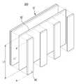
도 1은 본 발명의 일 실시예에 따른 표시 장치의 분해 사시도이고, 도 2는 도 1에 도시한 표시 장치에 포함된 유기 발광 표시 모듈의 부분 분해 사시도이다.FIG. 1 is an exploded perspective view of a display device according to an embodiment of the present invention, and FIG. 2 is a partially exploded perspective view of an OLED display module included in the display device shown in FIG.
도 1 및 도 2를 참조하면, 일 실시예에 따른 표시 장치(100)는 영상을 표시하는 표시 패널(10)과 표시 패널(10)의 후방에서 표시 패널(10)과 결합되어 이를 지지하는 브래킷(20)을 포함하는 유기 발광 표시 모듈(30), 브래킷(20)의 배면에 구비되는 인쇄회로기판(미도시), 브래킷(20)에 결합되는 프론트 캐비닛(40)과 리어 캐비닛(50)를 포함한다.1 and 2, a
표시 패널(10)은 서로 마주하여 실런트로 부착되는 제1 기판(12)과 제2 기판(14)을 포함한다. 제1 기판(12)과 제2 기판(14)의 중첩 영역에는, 실제 영상 표시가 이루어지는 표시 영역(A10)이 위치하고, 표시 영역(A10)의 외측에 비표시 영역(A20)이 위치할 수 있다.The
제1 기판(12)의 표시 영역(A10)에는 부화소들이 매트릭스 형태로 배치된다. 일례를 들면, 제1 기판(12)의 비표시 영역(A20)에는 부화소들과 인쇄회로기판 사이에 전기적인 신호를 전달하기 위한 패드 전극들(미도시)이 구비된다.In the display area A10 of the
패드 전극들은 연성 회로기판(미도시)을 통하여 인쇄회로기판에 연결된다. 예를 들면, 연성 회로기판은 비표시 영역(A20)에 칩 온 필름(chip on film: COF) 방식으로 구비되어, 브래킷(20)의 후방에 배치된 인쇄회로기판과 전기적으로 연결된다.The pad electrodes are connected to the printed circuit board through a flexible circuit board (not shown). For example, the flexible circuit board is provided in a non-display area A20 in a chip on film (COF) manner and is electrically connected to a printed circuit board disposed behind the
인쇄회로기판은 부화소들을 구동시키기 위한 스캔 드라이버(미도시)와 데이터 드라이버(미도시)를 실장한다. 브래킷(20)의 후방에 제어보드(미도시)를 별도로 구비할 수 있다. 제어보드는 전기 소자들(미도시)을 실장하여, 외부 신호에 따라 구동 신호를 처리하여 인쇄회로기판에 전송한다.The printed circuit board includes a scan driver (not shown) and a data driver (not shown) for driving sub-pixels. A control board (not shown) may be separately provided at the rear of the
도 3은 도 1에 도시한 표시 패널의 부화소 회로 구조를 나타낸 개략도이고, 도 4는 도 1에 도시한 패널 어셈블리의 부분 확대 단면도이다.FIG. 3 is a schematic view showing a sub-pixel circuit structure of the display panel shown in FIG. 1, and FIG. 4 is a partially enlarged sectional view of the panel assembly shown in FIG.
도 3 및 도 4를 참조하면, 표시 패널(10)의 부화소는 유기 발광 소자(L1)와 구동 회로부로 이루어진다. 유기 발광 소자(L1)는 애노드 전극(16)과 유기 발광층(18) 및 캐소드 전극(22)을 포함한다.Referring to FIGS. 3 and 4, the sub-pixel of the
구동 회로부는 적어도 2개의 박막 트랜지스터와 적어도 하나의 저장 캐패시터(C1)를 포함한다. 박막 트랜지스터는 기본적으로 스위칭 트랜지스터(T1)와 구동 트랜지스터(T2)를 포함한다.The driving circuit portion includes at least two thin film transistors and at least one storage capacitor (C1). The thin film transistor basically includes a switching transistor T1 and a driving transistor T2.
스위칭 트랜지스터(T1)는 스캔 라인(SL1)과 데이터 라인(DL1)에 연결되고, 스캔 라인(SL1)에 입력되는 스위칭 전압에 따라 데이터 라인(DL1)에서 입력되는 데이터 전압을 구동 트랜지스터(T2)로 전송한다.The switching transistor T1 is connected to the scan line SL1 and the data line DL1 and supplies a data voltage input from the data line DL1 to the driving transistor T2 according to a switching voltage input to the scan line SL1 send.
저장 캐패시터(C1)는 스위칭 트랜지스터(T1)와 전원 라인(VDD)에 연결되며, 스위칭 트랜지스터(T1)로부터 전송되는 전압과 전원 라인(VDD)에서 공급되는 전압의 차이에 해당하는 전압을 저장한다.The storage capacitor C1 is connected to the switching transistor T1 and the power supply line VDD and stores a voltage corresponding to a difference between a voltage transmitted from the switching transistor T1 and a voltage supplied from the power supply line VDD.
구동 트랜지스터(T2)는 전원 라인(VDD)과 저장 캐패시터(C1)에 연결되어 저장 캐패시터(C1)에 저장된 전압과 문턱 전압의 차이의 제곱에 비례하는 출력 전류(IOLED)를 유기발광 소자(L1)로 공급한다. 유기발광 소자(L1)는 출력 전류(IOLED)에 의해 발광한다.A driving transistor (T2) is a power supply line (VDD) and the output current (IOLED) that is proportional to the square of the difference between the voltage and the threshold voltage stored in the storage capacitor (C1) is connected to a storage capacitor (C1) an organic light emitting element (L1 ). The organic light emitting element L1 emits light by the output current IOLED .
구동 트랜지스터(T2)는 소스 전극(24)과 드레인 전극(26) 및 게이트 전극(28)을 포함하며, 유기발광 소자(L1)의 애노드 전극(16)이 구동 트랜지스터(T1)의 드레인 전극(26)에 연결될 수 있다. 부화소의 구성은 전술한 예에 한정되지 않고 다양하게 변형 가능하다.The driving transistor T2 includes a
다시 도 1 및 도 2를 참조하면, 유기 발광 표시 모듈(30)에 있어, 표시 패널(10)과 브래킷(20) 사이에는 제1 시트(22)와 제2 시트(24)의 이중 구조로 이루어진 시트 구조체가 배치된다.1 and 2, the organic light emitting
여기서, 제1 시트(22)는 열확산 기능을 지니며, 제2 시트(24)는 충격 흡수 기능을 지닌다. 구체적으로 제1 시트(22)는 열전도도가 높은 재질 예를 들어, 그라파이트, 구리, 알루미늄 중 어느 하나의 재질을 선택하여 이루어질 수 있다. 또한, 제2 시트(24)는 표시 장치(100)의 외부로부터 가해지는 충격이 유기 발광 표시 모듈(30)로 미치는 것을 방지할 수 있도록 충격 흡수가 가능한 재질 예를 들어 폴리에틴렌(polyethylene, PE) 또는 저밀도 폴리에틸렌(low-density polyethylene, LDPE)로 이루어질 수 있다. 제2 시트(24)는 그 내부에 공기 공동(air cavity, 24a)가 형성된 다공성 시트로 마련될 수 있다. 이러한 제2 시트(24)는 제1 시트(22)에 비해 상대적으로 열전도도가 낮다.Here, the
한편, 본 실시예에서, 유기 발광 표시 모듈(30)은, 텔레비젼과 같은 대형 모듈으로 형성된다. 그러나 본 발명의 유기 발광 표시 모듈이 반드시 이로 한정되는 것은 아니며, 중형 또는 소형으로도 마련될 수 있다.On the other hand, in this embodiment, the organic light emitting
본 실시예에서, 표시 패널(10)이 한쌍의 장변과 한쌍의 단변을 갖는 사각형으로 이루어짐에 따라, 제1 시트(22) 및 제2 시트(24)로 이에 대응하는 사각형으로 이루어진다.In this embodiment, the
이를 구체적으로 살펴보면, 제1 시트(22)는 표시 패널(10)의 전체 크기에 대응하는 크기를 가지고 표시 패널(10)의 전면(全面)에 밀착된다. 제2 시트(24)도 실질적으로 브래킷(20)의 전면(全面)에 대응하는 크기를 가지고 브래킷(20)에 밀착된다. 이에 따라 제1 시트(22)와 제2 시트(24)는 마주하는 면을 서로 밀착시키면서 표시 패널(10)과 브래킷(20) 사이에 개재된다. 이 때, 제1 시트(22) 및 제2 시트(24)는 각기 그 두께를 1㎜ 로 이룰 수 있다.Specifically, the
이와 같은 시트 구조체를 포함한 유기 발광 표시 모듈(30)이 그 전,후면에 배치되는 프론트 캐비닛(40)과 리어 캐비닛(50)과 조립되어 표시 장치(100)를 이루게 되면, 유기 발광 표시 모듈(30)과 이를 갖는 표시 장치(100)는, 내충격 및 방열 특성을 향상시킬 수 있게 된다.When the organic light emitting
즉, 표시 장치(100)의 외부로부터 충격이 가해지더라도, 충격 흡수 특성을 지닌 제2 시트(24)에 의해 충격 에너지가 표시 패널(10)로 직접 가해지는 방지할 수 있으므로, 유기 발광 표시 모듈(30)과 표시 장치(100)는, 내충격 특성을 향상시킬 수 있다.That is, even if an impact is applied from the outside of the
더욱이, 제2 시트(24)는 열전도도 낮은 재질로 구비됨에 따라, 표시 장치(100)의 구동시, 브래킷(50)의 후면에 장착된 인쇄회로기판에 구성되어, 표시 패널(10)을 구동시키기 위해 작동하는 회부로부터 발생되는 열이 표시 패널(10)로 직접적으로 전달되는 것을 차단시킬 수 있다. 이로 인해 표시 패널(10)은 외부로부터 가해지는 열에 의해 영향을 받아 오작동되는 피해를 방지할 수 있다.The
반면, 제1 시트(22)는, 열전도도가 우수하므로, 표시 패널(10)에서 발열되는 열 에너지를 확산시켜 표시 장치(100) 외부로 방출시킬 수 있다. 이에 표시 패널(10)은 외부로부터 받을 수 있는 열 에너지는 제2 시트(24)로 막고, 내부로부터 발생된 열 에너지는 제1 시트(22)로 방출할 수 있어, 이에 따라 표시 영역(A10) 전반에 대한 온도 분포를 균일하게 하여 양질의 화상을 표현할 수 있게 된다.On the other hand, since the
한편, 본 실시예에 제1 시트(22)와 제2 시트(24)는 실질적으로 같은 크기로 형성되는 경우로 설명되었으나, 본 발명의 시트 구조체가 반드시 이의 경우로 한정되는 것은 아니다. 이하에서는 이의 다른 실시예에 대해 알아 보도록 한다.Although the
도 5는 본 발명의 제2 실시예에 따른 유기 발광 표시 모듈(200)을 도시한 분해 사시도이다.5 is an exploded perspective view illustrating an
이 유기 발광 표시 모듈(200)은, 전술한 유기 발광 표시 모듈에 대비하여 제2 시트의 형상만을 달리한다. 즉, 도 1,2에 도시한 것과 같은, 표시 패널(10)에 제1 시트(20)가 제공되고, 이 제1 시트(20) 상에는 이 제1 시트(20)보다 작은 크기를 갖는 제2 시트(62)가 분리 배치된다.The organic light emitting
제2 시트(62)는 스트라이프 형상을 가지면서, 표시 패널(10) 및 제1 시트(22)의 단변을 따라 배치되도록 제1 시트(20)와 마주한다. 이때, 제2 시트(62)의 길이(L1)는, 제1 시트(22)의 단변 길이(L2)와 동일하나, 필요에 따라 이의 길이(L1)는 적절하게 조절될 수 있다.The
이러한 제2 시트(62)는 복수개로 구비되어 제1 시트(20) 상에 등간격을 두고 배치된다.A plurality of such
도 6는 본 발명의 제3 실시예에 따른 유기 발광 표시 모듈(300)을 도시한 분해 사시도이다. 이 유기 발광 표시 모듈(300) 역시, 도 1,2에 도시한 유기 발광 표시 모듈과 같은 표시 패널과 제1 시트를 가지면서 제2 시트의 형상만을 달리하여 구성된다.6 is an exploded perspective view illustrating an
도 6을 참조하면, 유기 발광 표시 모듈(300)은 표시 패널(10), 제1 시트(22) 및 제2 시트(64)를 포함하며, 제2 시트(64)가 제1 시트(22) 상에 체크 패턴을 이루도록 배치된다. 도 6에서는 제2 시트(64)가 대략 정사각형의 형상을 가지면서 상호간 접촉하지 않고 체크 패턴을 만들어 제1 시트(22)에 배열되는 경우로 도시하고 있으나, 이 제2 시트(64)는 체크 패턴을 유지하되, 그 형상이나 접촉 관계는 도 6의 상태로 한정되지는 않는다.6, the
한편, 전술한 실시예들에 있어 브래킷은, 통상의 브래킷과 같이 하나의 판재 형태로 구비되나, 본 발명에 있어 브래킷은 다른 형태로도 구비 가능하다.Meanwhile, in the above-described embodiments, the bracket is provided in the form of one plate like a normal bracket, but the bracket may be provided in other forms in the present invention.
이하 도 7 내지 도 9를 본 발명의 제4 실시예에 따른 유기 발광 표시 모듈을 설명하도록 한다.7 to 9 illustrate an OLED display module according to a fourth embodiment of the present invention.
도 7을 참조하면, 유기 발광 표시 모듈(400)은, 표시 패널(10)과 브래킷(70), 이들 사이에 개재되는 시트 구조체를 포함한다. 여기서 시트 구조체는 도 1,2에 도시한 시트 구조체와 동일한 제1 시트(22)와 제2 시트(24)로 이루어지나, 도 5 및 도 6에 도시한 시트 구조체로도 적용 가능하다.Referring to FIG. 7, the organic light emitting display module 400 includes a
제4 실시예의 브래킷(70)은, 제1 플레이트(72), 제2 플레이트(74) 및 격벽(76)을 포함한다.The
제 1 플레이트(72)는 대략 직사각형 형상을 갖는다. 제 1 플레이트(72)는 시트 구조체에 맞대어져서, 표시 패널(10)과 연결되어 이를 지지한다.The
제 2 플레이트(74)는 제 1 플레이트(72)의 상부에 배치된다. 따라서, 제 2 플레이트(74)는 제 1 플레이트(72)와 대향한다. 제 2 플레이트(74)는 대략 직사각형 형상을 갖는다.A second plate (74) is disposed on top of the first plate (72). Thus, the
격벽(76)은 제 1 플레이트(72)와 제 2 플레이트(74) 사이에 개재된다. 격벽(76)은 제 1 플레이트(72)의 상부면에 연결된 하단, 및 제 2 플레이트(74)의 하부면에 연결된 상단을 갖는다. 도 8에 도시된 바와 같이, 격벽(76)은 제 1 플레이트(72)와 제 2 플레이트(74) 사이의 공간을 허니컴 구조로 구획한다.The
허니컴 구조의 격벽(76)은 주지된 바와 같이 매우 강한 강도를 갖는다. 또한, 허니컴 구조의 격벽(76)은 표시 패널(10)에서 발생된 열이 제 1 플레이트(72)로부터 제 2 플레이트(74)를 향하는 제 1 방향으로 전달되는 것을 억제한다. 반면에, 허니컴 구조의 격벽(76)은 표시 패널(10)에서 발생된 열을 제 1 방향과 실질적으로 직교하는 제 2 방향으로 분산시킨다. 결과적으로, 표시 패널(10)에서 발생된 열은 허니컴 구조의 격벽(76)을 통해서 신속하게 외부로 방출될 수 있다.The
제4 실시예에서, 제 1 플레이트(72), 제 2 플레이트(74) 및 격벽(76)은 동일한 재질을 포함할 수 있다. 예를 들어서, 제 1 플레이트(72), 제 2 플레이트(74) 및 격벽(76)은 알루미늄 등과 같은 금속 재질을 포함할 수 있다. 이와 같이, 제 1 플레이트(72), 제 2 플레이트(74) 및 격벽(76)이 동일한 재질을 포함하므로, 브래킷(70)은 불연속면을 갖지 않게 된다. 결과적으로, 표시 패널(10)의 온도 분포에서도 불연속선이 발생하지 않게 된다.In the fourth embodiment, the
또한, 본 제4 실시예에서, 제 2 플레이트(74)는 제 1 플레이트(72)의 면적보다 좁은 면적을 갖는다. 따라서, 제 1 플레이트(72)의 가장자리(720)가 제 2 플레이트(74)에 의해 차단되지 않고 노출된다. 즉, 제 1 플레이트(72)의 가장자리 상부에 외곽 플레이트(78)를 수용하는 공간이 형성된다. 여기서, 제 1 플레이트(72)의 가장자리(720)는 표시 패널(10)의 비표시 영역(A20)과 대응한다. 따라서, 제 2 플레이트(74)는 표시 패널(10)의 표시 영역(A10)의 면적과 실질적으로 동일한 면적을 가질 수 있다.Further, in the fourth embodiment, the
다른 한편으로, 제 1 플레이트(72)와 동일한 면적을 갖는 제 2 플레이트(74)의 가장자리를 압축 공정을 통해서 제거하여, 제 1 플레이트(72)보다 좁은 면적을 갖는 제 2 플레이트(74)를 성형할 수도 있다. 허니컴 구조의 브래킷(70)은 매우 낮은 용적비를 갖고 있으므로, 제 2 플레이트(74)의 가장자리를 용이하게 압축시킬 수 있다.On the other hand, the edge of the
외곽 플레이트(78)는 브래킷(70)의 4면에 설치되는 4개의 부재들로 이루어질 수 있다.The
본 실시예에서, 외곽 플레이트(78)는 양면 테이프, 접착제 등을 이용해서 브래킷(70)에 부착될 수 있다.In this embodiment, the
다른 실시예로서, 외곽 플레이트(70)를 지그에 고정시킨 상태에서, 브래킷(70)의 압축된 가장자리를 외곽 플레이트(78)에 조립시킬 수도 있다. 이러한 경우, 외곽 플레이트(78)의 위치가 미리 결정되어 있으므로, 제 2 플레이트(74)의 가장자리를 압축하여 절단하는 공정은 여유로운 공차를 가지게 된다.In another embodiment, the compressed edge of the
본 실시예에서, 외곽 플레이트(78)는 제 1 플레이트(72)의 노출면, 즉 가장자리에 배치된다. 전술한 바와 같이, 제 1 플레이트(72)의 가장자리는 표시 패널(10)의 비표시 영역(A20)에 해당하므로, 외곽 플레이트(78)도 표시 패널(10)의 비표시 영역(A20) 내에 위치하게 된다. 따라서, 외곽 플레이트(78)로 인해서 표시 패널(10)의 표시 품질이 저해되지 않는다. 구체적으로, 표시 패널(10)의 표시 품질을 저해하는 주된 요소는 외곽 플레이트(78)와 제 1 플레이트(72) 사이의 경계선(I)이다. 경계선(I)은 표시 패널(10)의 영역 내에 위치한다. 그러므로, 외곽 플레이트(78)와 제 1 플레이트(72) 사이의 경계선(I)으로 인해서, 표시 패널(10)의 표시 품질이 저해되는 것이 방지된다.In this embodiment, the
또한, 본 실시예에서, 외곽 플레이트(78)는 제 1 및 제 2 플레이트(72, 74)들 및 격벽(76)과 실질적으로 동일한 재질을 포함할 수 있다. 즉, 외곽 플레이트(78)는 알루미늄 등과 같은 금속 재질을 포함할 수 있다. 따라서, 외곽 플레이트(78)가 브래킷(70)과 실질적으로 동일한 재질을 포함하므로, 외곽 플레이트(78)가 표시 패널(10)의 표시 품질에 거의 영향을 주지 않게 된다.Further, in this embodiment, the
아울러, 본 제4 실시예에서, 외곽 플레이트(78)는 제 1 플레이트(72)의 내측면으로부터 제 2 플레이트(74)의 외측면까지의 거리(H)와 실질적으로 동일하거나 또는 얇은 두께(T)를 갖는다. 여기서, 제 1 플레이트(72)의 내측면은 제 2 플레이트(74)를 향하는 면이고, 제 2 플레이트(74)의 외측면은 제 1 플레이트(72)의 반대를 향하는 면이다. 즉, 외곽 플레이트(78)의 두께(T)는 제 1 플레이트(72)의 내측면과 제 2 플레이트(74)의 외측면 사이의 거리(H) 이하이다. 따라서, 제 1 플레이트(72)의 가장자리에 배치된 외곽 플레이트(78)는 제 2 플레이트(74)의 외측면보다 돌출되지 않는다. 결과적으로, 외곽 플레이트(78)의 두께가 브래킷(70)의 두께에 합산되지 않는다. 즉, 브래킷(70)의 두께는 오직 제 1 플레이트(72)의 외측면으로부터 제 2 플레이트(74)의 외측면까지의 거리에 해당한다. 이와 같이, 외곽 플레이트(78)로 인해서 브래킷(70)의 두께가 증가되지 않으므로, 본 실시예의 허니컴 구조의 브래킷(70)은 얇은 두께를 가지면서도 무거운 표시 패널(10)을 견고하게 지지할 수가 있다.In addition, in the fourth embodiment, the
이상을 통해 본 발명의 바람직한 실시예에 대하여 설명하였지만, 본 발명은 이에 한정되는 것이 아니고 특허청구범위와 발명의 상세한 설명 및 첨부한 도면의 범위 안에서 여러 가지로 변형하여 실시하는 것이 가능하고 이 또한 본 발명의 범위에 속하는 것은 당연하다.While the present invention has been particularly shown and described with reference to exemplary embodiments thereof, it is to be understood that the invention is not limited to the disclosed exemplary embodiments, but, on the contrary, And it goes without saying that the invention belongs to the scope of the invention.
10: 표시 패널, 20, 70: 브래킷, 22: 제1 시트,
24, 62, 64: 제2 시트, 30, 200, 300, 400: 유기 발광 표시 모듈,
40: 프론트 캐비닛, 50: 리어 캐니빗, 72: 제1 플레이트, 74: 제2 플레이트, 76: 격벽, 78: 외곽 플레이트, 100: 표시 장치
A10: 표시 영역, A20: 비표시영역10: display panel, 20, 70: bracket, 22: first sheet,
24, 62, 64: second sheet, 30, 200, 300, 400: organic light emitting display module,
The present invention relates to a front cabinet and a rear cabinet which are provided with a front plate and a rear plate,
A10: display area, A20: non-display area
Claims (22)
Translated fromKorean상기 표시 패널에 결합되어 상기 표시 패널을 지지하는 브래킷; 및
상기 표시 패널과 상기 브래킷 사이에 개재되는 시트 구조체
를 포함하고,
상기 시트 구조체는,
열확산을 위한 제1 시트; 및
충격 흡수를 위한 제2 시트
를 포함하는 유기 발광 표시 모듈.A display panel including an organic light emitting element;
A bracket coupled to the display panel to support the display panel; And
And a sheet structure interposed between the display panel and the bracket
Lt; / RTI >
The sheet structure may include:
A first sheet for thermal diffusion; And
The second sheet for shock absorption
And an organic light emitting display module.
상기 제1 시트는 상기 표시 패널에 밀착되고, 상기 제2 시트는 상기 브래킷에 밀착되는, 유기 발광 표시 모듈.The method according to claim 1,
Wherein the first sheet is in close contact with the display panel, and the second sheet is in close contact with the bracket.
상기 제1 시트는 상기 표시 패널의 전면(全面)에 대응하는 크기를 가지고, 상기 제2 시트는 상기 브래킷의 전면(全面)에 대응하는 크기를 갖는, 유기 발광 표시 모듈.3. The method of claim 2,
Wherein the first sheet has a size corresponding to the entire surface of the display panel and the second sheet has a size corresponding to the entire surface of the bracket.
상기 제1 시트는 상기 표시 패널의 전면(全面)에 대응하는 크기를 가지고, 상기 제2 시트는 상기 제1 시트보다 작은 크기를 가지고 상기 제1 시트 상에 분리 배치되는, 유기 발광 표시 모듈.3. The method of claim 2,
Wherein the first sheet has a size corresponding to the entire surface of the display panel and the second sheet has a size smaller than that of the first sheet and is disposed on the first sheet.
상기 제2 시트는 스트라이프 패턴을 가지고 상기 제1 시트 상에 등간격을 두고 배치되는, 유기 발광 표시 모듈.5. The method of claim 4,
Wherein the second sheet has a stripe pattern and is disposed at equal intervals on the first sheet.
상기 제1 시트는 한 쌍의 장변과 한 쌍의 단변을 갖는 사각형상으로 이루어지고, 상기 제2 시트는 상기 제1 시트의 단변을 따라 배치되는, 유기 발광 표시 모듈.6. The method of claim 5,
Wherein the first sheet has a rectangular shape having a pair of long sides and a pair of short sides, and the second sheet is disposed along a short side of the first sheet.
상기 제2 시트의 길이와 상기 제1 시트의 단변 길이가 동일한, 유기 발광 표시 모듈.The method according to claim 6,
And the length of the second sheet is equal to the length of the short side of the first sheet.
상기 제2 시트는, 상기 제1 시트 상에 체크 패턴으로 배치되는, 유기 발광 표시 모듈.5. The method of claim 4,
And the second sheet is arranged in a check pattern on the first sheet.
상기 제2 시트는 다공성 시트인, 유기 발광 표시 모듈.The method according to claim 1,
And the second sheet is a porous sheet.
상기 제1 시트 및 상기 제2 시트의 각각의 두께가 1㎜ 인, 유기 발광 표시 모듈.The method according to claim 1,
And each of the first sheet and the second sheet has a thickness of 1 mm.
상기 브래킷은,
상기 표시 패널에 대향하는 제 1 플레이트;
상기 제 1 플레이트와 대향하고, 상기 제 1 플레이트보다 좁은 면적을 갖는 제 2 플레이트; 및
상기 제 1 플레이트와 상기 제 2 플레이트 사이에 개재된 격벽
을 포함하는 유기 발광 표시 모듈.The method according to claim 1,
The bracket
A first plate facing the display panel;
A second plate facing the first plate and having a smaller area than the first plate; And
And a partition plate interposed between the first plate and the second plate,
Emitting layer.
상기 제 1 플레이트의 가장자리가 상기 제 2 플레이트로부터 노출된 유기 발광 표시 모듈.12. The method of claim 11,
And an edge of the first plate is exposed from the second plate.
상기 제 1 플레이트의 가장자리에 배치되어 상기 표시 패널에 고정되는 외곽 플레이트를 더욱 포함하는 유기 발광 표시 모듈.13. The method of claim 12,
And an outer plate disposed at an edge of the first plate and fixed to the display panel.
상기 외곽 플레이트는 상기 제 1 플레이트의 노출면으로부터 상기 제 2 플레이트의 외측면까지의 거리 이하의 두께를 갖는 유기 발광 표시 모듈.14. The method of claim 13,
Wherein the outer plate has a thickness equal to or less than a distance from an exposed surface of the first plate to an outer surface of the second plate.
상기 외곽 플레이트는 상기 제 1 및 제 2 플레이트들 및 상기 격벽과 동일한 재질을 포함하는 유기 발광 표시 모듈.14. The method of claim 13,
Wherein the outer plate comprises the same material as the first and second plates and the partition.
상기 제 1 및 제 2 플레이트, 상기 격벽 및 상기 외곽 플레이트는 알루미늄을 포함하는 유기 발광 표시 모듈.16. The method of claim 15,
Wherein the first and second plates, the partition, and the outline plate comprise aluminum.
상기 격벽은 허니컴 형상을 갖는 유기 발광 표시 모듈.12. The method of claim 11,
And the partition wall has a honeycomb shape.
상기 제1 시트가 그라파이트, 구리, 알루미늄 중 어느 하나로 선택되어 이루어진, 유기 발광 표시 모듈.11. The method according to any one of claims 1 to 10,
Wherein the first sheet is selected from the group consisting of graphite, copper, and aluminum.
상기 제2 시트가 폴리에틸렌 또는 저밀도 폴리에틸렌으로 이루어진, 유기 발광 표시 모듈.11. The method according to any one of claims 1 to 10,
Wherein the second sheet is made of polyethylene or low density polyethylene.
상기 표시 패널 측에 배치되어 상기 표시 패널의 일면 외곽과 측면을 둘러싸는 프론트 캐비닛; 및
상기 브래킷 측에 배치되어 상기 브래킷을 덮으며 상기 프론트 캐비닛에 결합되는 리어 캐비닛
을 포함하는 표시 장치.An organic light emitting display module according to any one of claims 1 to 18,
A front cabinet disposed on the display panel side and surrounding one side surface and side surfaces of the display panel; And
A rear cabinet disposed on the bracket side to cover the bracket and coupled to the front cabinet,
.
상기 제1 시트가 그라파이트, 구리, 알루미늄 중 어느 하나로 선택되어 이루어진, 표시 장치.21. The method of claim 20,
Wherein the first sheet is selected from any one of graphite, copper, and aluminum.
상기 제2 시트가 폴리에틸렌 또는 저밀도 폴리에틸렌으로 이루어진, 표시 장치.21. The method of claim 20,
And the second sheet is made of polyethylene or low density polyethylene.
Priority Applications (5)
| Application Number | Priority Date | Filing Date | Title |
|---|---|---|---|
| KR1020130062965AKR20140141330A (en) | 2013-05-31 | 2013-05-31 | Organic light emitting display moduled and display device having the same |
| US14/100,751US20140353623A1 (en) | 2013-05-31 | 2013-12-09 | Organic light emitting display module and display device including the same |
| TW103104659ATW201445727A (en) | 2013-05-31 | 2014-02-13 | Organic light emitting display module and display device therewith |
| EP14158801.2AEP2808894A1 (en) | 2013-05-31 | 2014-03-11 | Organic light emitting display module and display device including the same |
| CN201410125987.XACN104218057A (en) | 2013-05-31 | 2014-03-31 | Organic light-emitting display apparatus and method of manufacturing the same |
Applications Claiming Priority (1)
| Application Number | Priority Date | Filing Date | Title |
|---|---|---|---|
| KR1020130062965AKR20140141330A (en) | 2013-05-31 | 2013-05-31 | Organic light emitting display moduled and display device having the same |
Publications (1)
| Publication Number | Publication Date |
|---|---|
| KR20140141330Atrue KR20140141330A (en) | 2014-12-10 |
Family
ID=50238278
Family Applications (1)
| Application Number | Title | Priority Date | Filing Date |
|---|---|---|---|
| KR1020130062965ACeasedKR20140141330A (en) | 2013-05-31 | 2013-05-31 | Organic light emitting display moduled and display device having the same |
Country Status (5)
| Country | Link |
|---|---|
| US (1) | US20140353623A1 (en) |
| EP (1) | EP2808894A1 (en) |
| KR (1) | KR20140141330A (en) |
| CN (1) | CN104218057A (en) |
| TW (1) | TW201445727A (en) |
Cited By (4)
| Publication number | Priority date | Publication date | Assignee | Title |
|---|---|---|---|---|
| US9763368B2 (en) | 2015-02-03 | 2017-09-12 | Samsung Display Co., Ltd. | Display device |
| US9935278B2 (en) | 2015-03-10 | 2018-04-03 | Samsung Display Co., Ltd. | Display apparatus and portable terminal |
| US10619943B2 (en) | 2016-11-25 | 2020-04-14 | Samsung Display Co., Ltd. | Composite sheet, method of fabricating the same, and display device comprising the same |
| WO2022050697A1 (en)* | 2020-09-02 | 2022-03-10 | 주식회사 엘지화학 | Buffer film |
Families Citing this family (5)
| Publication number | Priority date | Publication date | Assignee | Title |
|---|---|---|---|---|
| US9658659B2 (en)* | 2013-01-10 | 2017-05-23 | Lg Electronics Inc. | Display device |
| US10270065B2 (en) | 2017-06-26 | 2019-04-23 | Shenzhen China Star Optoelectronics Technology Co., Ltd. | Heat radiation structure for organic light-emitting device and display apparatus |
| CN107221556A (en)* | 2017-06-26 | 2017-09-29 | 深圳市华星光电技术有限公司 | Radiator structure and display device for organic luminescent device |
| KR102367975B1 (en) | 2017-07-06 | 2022-02-25 | 삼성디스플레이 주식회사 | Panel bottom member and display device including the same |
| KR102430953B1 (en)* | 2017-12-21 | 2022-08-09 | 삼성디스플레이 주식회사 | Panel bottom member and display device including the same |
Family Cites Families (16)
| Publication number | Priority date | Publication date | Assignee | Title |
|---|---|---|---|---|
| US5666261A (en)* | 1995-09-25 | 1997-09-09 | At&T Global Information Solutions Company | Honeycomb celled-sheet layer composite panel for monitoring an LCD to a laptop computer |
| KR100529112B1 (en)* | 2003-09-26 | 2005-11-15 | 삼성에스디아이 주식회사 | Display apparatus having porous heat transfer sheet |
| KR100669696B1 (en)* | 2003-11-08 | 2007-01-16 | 삼성에스디아이 주식회사 | Plasma display |
| KR100719534B1 (en)* | 2004-08-05 | 2007-05-17 | 삼성에스디아이 주식회사 | Plasma display device |
| KR100978045B1 (en)* | 2006-03-13 | 2010-08-26 | 삼성전자주식회사 | Liquid crystal panel assembly and liquid crystal display device comprising the same |
| KR101189154B1 (en)* | 2006-06-08 | 2012-11-09 | 삼성디스플레이 주식회사 | Organic Light Emitting Display Device |
| KR100769425B1 (en)* | 2006-09-21 | 2007-10-22 | 삼성에스디아이 주식회사 | Organic light emitting display |
| KR100962218B1 (en)* | 2008-12-01 | 2010-06-11 | 한국생산기술연구원 | The large-area oled lighting panel with a radiant heat wire and lighting system with a low-contact-resistance |
| JP5672705B2 (en)* | 2010-01-26 | 2015-02-18 | 住友化学株式会社 | Light emitting device and manufacturing method thereof |
| US8851736B2 (en)* | 2011-08-30 | 2014-10-07 | Lg Innotek Co., Ltd. | Light emitting module with heatsink plate having coupling protrusions |
| KR101945890B1 (en)* | 2011-12-30 | 2019-02-12 | 삼성전자주식회사 | Display device |
| KR101190630B1 (en)* | 2012-01-30 | 2012-10-15 | 주식회사 지앤씨에스 | Organic light emitting diode display |
| US9395036B2 (en)* | 2012-06-13 | 2016-07-19 | Samsung Display Co., Ltd. | Bracket for a display panel and display device including the same |
| KR20140006378A (en)* | 2012-07-04 | 2014-01-16 | 삼성전자주식회사 | Display device |
| EP2685444B1 (en)* | 2012-07-13 | 2017-03-08 | LG Electronics, Inc. | Display device using sandwich honeycomb panel |
| KR101888910B1 (en)* | 2012-08-03 | 2018-08-20 | 삼성전자주식회사 | Display apparatus |
- 2013
- 2013-05-31KRKR1020130062965Apatent/KR20140141330A/ennot_activeCeased
- 2013-12-09USUS14/100,751patent/US20140353623A1/ennot_activeAbandoned
- 2014
- 2014-02-13TWTW103104659Apatent/TW201445727A/enunknown
- 2014-03-11EPEP14158801.2Apatent/EP2808894A1/ennot_activeWithdrawn
- 2014-03-31CNCN201410125987.XApatent/CN104218057A/enactivePending
Cited By (6)
| Publication number | Priority date | Publication date | Assignee | Title |
|---|---|---|---|---|
| US9763368B2 (en) | 2015-02-03 | 2017-09-12 | Samsung Display Co., Ltd. | Display device |
| US9935278B2 (en) | 2015-03-10 | 2018-04-03 | Samsung Display Co., Ltd. | Display apparatus and portable terminal |
| US10276810B2 (en) | 2015-03-10 | 2019-04-30 | Samsung Display Co., Ltd. | Curved display apparatus with buffer |
| US10619943B2 (en) | 2016-11-25 | 2020-04-14 | Samsung Display Co., Ltd. | Composite sheet, method of fabricating the same, and display device comprising the same |
| US11280558B2 (en) | 2016-11-25 | 2022-03-22 | Samsung Display Co., Ltd. | Composite sheet, method of fabricating the same, and display device comprising the same |
| WO2022050697A1 (en)* | 2020-09-02 | 2022-03-10 | 주식회사 엘지화학 | Buffer film |
Also Published As
| Publication number | Publication date |
|---|---|
| TW201445727A (en) | 2014-12-01 |
| CN104218057A (en) | 2014-12-17 |
| US20140353623A1 (en) | 2014-12-04 |
| EP2808894A1 (en) | 2014-12-03 |
Similar Documents
| Publication | Publication Date | Title |
|---|---|---|
| KR20140141330A (en) | Organic light emitting display moduled and display device having the same | |
| KR102119532B1 (en) | Display apparatus | |
| KR101940761B1 (en) | Organic Light Emitting diode display | |
| US10046536B2 (en) | Composite sheet and display device including the same | |
| US20120293960A1 (en) | Display device | |
| KR20140092170A (en) | Display apparatus | |
| JP2009157131A (en) | Plasma display device | |
| KR100922356B1 (en) | Organic light emitting display | |
| KR100922360B1 (en) | Organic light emitting display | |
| KR20140095851A (en) | Organic light emitting diode display | |
| KR20210120324A (en) | OLED display device | |
| TWI853355B (en) | Display apparatus and method for manufacturing the same | |
| KR101009645B1 (en) | Organic light emitting display | |
| US20090315879A1 (en) | Plasma display device | |
| KR101982257B1 (en) | Display apparatus | |
| KR102377974B1 (en) | Display device | |
| KR100626011B1 (en) | Plasma display device | |
| KR101082439B1 (en) | Plasma display module | |
| KR100670253B1 (en) | Chassis Base for Plasma Display and Plasma Display with Same | |
| KR100683703B1 (en) | Plasma display device | |
| KR101106315B1 (en) | Driving circuit board of plasma display panel and plasma display device having same | |
| KR100730163B1 (en) | Plasma display device | |
| KR100626053B1 (en) | Plasma display module | |
| KR20060055107A (en) | Plasma display apparatus | |
| KR100820638B1 (en) | Plasma display device |
Legal Events
| Date | Code | Title | Description |
|---|---|---|---|
| PA0109 | Patent application | Patent event code:PA01091R01D Comment text:Patent Application Patent event date:20130531 | |
| PG1501 | Laying open of application | ||
| A201 | Request for examination | ||
| PA0201 | Request for examination | Patent event code:PA02012R01D Patent event date:20180531 Comment text:Request for Examination of Application Patent event code:PA02011R01I Patent event date:20130531 Comment text:Patent Application | |
| E902 | Notification of reason for refusal | ||
| PE0902 | Notice of grounds for rejection | Comment text:Notification of reason for refusal Patent event date:20190522 Patent event code:PE09021S01D | |
| E902 | Notification of reason for refusal | ||
| PE0902 | Notice of grounds for rejection | Comment text:Notification of reason for refusal Patent event date:20191127 Patent event code:PE09021S01D | |
| E601 | Decision to refuse application | ||
| PE0601 | Decision on rejection of patent | Patent event date:20200428 Comment text:Decision to Refuse Application Patent event code:PE06012S01D Patent event date:20191127 Comment text:Notification of reason for refusal Patent event code:PE06011S01I Patent event date:20190522 Comment text:Notification of reason for refusal Patent event code:PE06011S01I |