KR20140136027A - Light-emitting element, light-emitting device, electronic device, and lighting device - Google Patents
Light-emitting element, light-emitting device, electronic device, and lighting deviceDownload PDFInfo
- Publication number
- KR20140136027A KR20140136027AKR1020147028262AKR20147028262AKR20140136027AKR 20140136027 AKR20140136027 AKR 20140136027AKR 1020147028262 AKR1020147028262 AKR 1020147028262AKR 20147028262 AKR20147028262 AKR 20147028262AKR 20140136027 AKR20140136027 AKR 20140136027A
- Authority
- KR
- South Korea
- Prior art keywords
- light emitting
- layer
- light
- organic compound
- emitting layer
- Prior art date
- Legal status (The legal status is an assumption and is not a legal conclusion. Google has not performed a legal analysis and makes no representation as to the accuracy of the status listed.)
- Granted
Links
Images


Classifications
- H—ELECTRICITY
- H10—SEMICONDUCTOR DEVICES; ELECTRIC SOLID-STATE DEVICES NOT OTHERWISE PROVIDED FOR
- H10K—ORGANIC ELECTRIC SOLID-STATE DEVICES
- H10K50/00—Organic light-emitting devices
- H10K50/10—OLEDs or polymer light-emitting diodes [PLED]
- H10K50/11—OLEDs or polymer light-emitting diodes [PLED] characterised by the electroluminescent [EL] layers
- H10K50/125—OLEDs or polymer light-emitting diodes [PLED] characterised by the electroluminescent [EL] layers specially adapted for multicolour light emission, e.g. for emitting white light
- H10K50/13—OLEDs or polymer light-emitting diodes [PLED] characterised by the electroluminescent [EL] layers specially adapted for multicolour light emission, e.g. for emitting white light comprising stacked EL layers within one EL unit
- C—CHEMISTRY; METALLURGY
- C09—DYES; PAINTS; POLISHES; NATURAL RESINS; ADHESIVES; COMPOSITIONS NOT OTHERWISE PROVIDED FOR; APPLICATIONS OF MATERIALS NOT OTHERWISE PROVIDED FOR
- C09K—MATERIALS FOR MISCELLANEOUS APPLICATIONS, NOT PROVIDED FOR ELSEWHERE
- C09K11/00—Luminescent, e.g. electroluminescent, chemiluminescent materials
- C09K11/06—Luminescent, e.g. electroluminescent, chemiluminescent materials containing organic luminescent materials
- H—ELECTRICITY
- H10—SEMICONDUCTOR DEVICES; ELECTRIC SOLID-STATE DEVICES NOT OTHERWISE PROVIDED FOR
- H10K—ORGANIC ELECTRIC SOLID-STATE DEVICES
- H10K50/00—Organic light-emitting devices
- H10K50/10—OLEDs or polymer light-emitting diodes [PLED]
- H10K50/11—OLEDs or polymer light-emitting diodes [PLED] characterised by the electroluminescent [EL] layers
- H10K50/12—OLEDs or polymer light-emitting diodes [PLED] characterised by the electroluminescent [EL] layers comprising dopants
- H10K50/121—OLEDs or polymer light-emitting diodes [PLED] characterised by the electroluminescent [EL] layers comprising dopants for assisting energy transfer, e.g. sensitization
- H—ELECTRICITY
- H10—SEMICONDUCTOR DEVICES; ELECTRIC SOLID-STATE DEVICES NOT OTHERWISE PROVIDED FOR
- H10K—ORGANIC ELECTRIC SOLID-STATE DEVICES
- H10K50/00—Organic light-emitting devices
- H10K50/10—OLEDs or polymer light-emitting diodes [PLED]
- H10K50/14—Carrier transporting layers
- H10K50/15—Hole transporting layers
- H—ELECTRICITY
- H10—SEMICONDUCTOR DEVICES; ELECTRIC SOLID-STATE DEVICES NOT OTHERWISE PROVIDED FOR
- H10K—ORGANIC ELECTRIC SOLID-STATE DEVICES
- H10K50/00—Organic light-emitting devices
- H10K50/10—OLEDs or polymer light-emitting diodes [PLED]
- H10K50/14—Carrier transporting layers
- H10K50/16—Electron transporting layers
- H—ELECTRICITY
- H10—SEMICONDUCTOR DEVICES; ELECTRIC SOLID-STATE DEVICES NOT OTHERWISE PROVIDED FOR
- H10K—ORGANIC ELECTRIC SOLID-STATE DEVICES
- H10K50/00—Organic light-emitting devices
- H10K50/10—OLEDs or polymer light-emitting diodes [PLED]
- H10K50/17—Carrier injection layers
- H10K50/171—Electron injection layers
- H—ELECTRICITY
- H10—SEMICONDUCTOR DEVICES; ELECTRIC SOLID-STATE DEVICES NOT OTHERWISE PROVIDED FOR
- H10K—ORGANIC ELECTRIC SOLID-STATE DEVICES
- H10K50/00—Organic light-emitting devices
- H10K50/80—Constructional details
- H10K50/805—Electrodes
- H10K50/81—Anodes
- H—ELECTRICITY
- H10—SEMICONDUCTOR DEVICES; ELECTRIC SOLID-STATE DEVICES NOT OTHERWISE PROVIDED FOR
- H10K—ORGANIC ELECTRIC SOLID-STATE DEVICES
- H10K50/00—Organic light-emitting devices
- H10K50/80—Constructional details
- H10K50/805—Electrodes
- H10K50/82—Cathodes
- H—ELECTRICITY
- H10—SEMICONDUCTOR DEVICES; ELECTRIC SOLID-STATE DEVICES NOT OTHERWISE PROVIDED FOR
- H10K—ORGANIC ELECTRIC SOLID-STATE DEVICES
- H10K50/00—Organic light-emitting devices
- H10K50/80—Constructional details
- H10K50/85—Arrangements for extracting light from the devices
- H—ELECTRICITY
- H10—SEMICONDUCTOR DEVICES; ELECTRIC SOLID-STATE DEVICES NOT OTHERWISE PROVIDED FOR
- H10K—ORGANIC ELECTRIC SOLID-STATE DEVICES
- H10K59/00—Integrated devices, or assemblies of multiple devices, comprising at least one organic light-emitting element covered by group H10K50/00
- H10K59/30—Devices specially adapted for multicolour light emission
- H10K59/35—Devices specially adapted for multicolour light emission comprising red-green-blue [RGB] subpixels
- H—ELECTRICITY
- H10—SEMICONDUCTOR DEVICES; ELECTRIC SOLID-STATE DEVICES NOT OTHERWISE PROVIDED FOR
- H10K—ORGANIC ELECTRIC SOLID-STATE DEVICES
- H10K59/00—Integrated devices, or assemblies of multiple devices, comprising at least one organic light-emitting element covered by group H10K50/00
- H10K59/30—Devices specially adapted for multicolour light emission
- H10K59/38—Devices specially adapted for multicolour light emission comprising colour filters or colour changing media [CCM]
- H—ELECTRICITY
- H10—SEMICONDUCTOR DEVICES; ELECTRIC SOLID-STATE DEVICES NOT OTHERWISE PROVIDED FOR
- H10K—ORGANIC ELECTRIC SOLID-STATE DEVICES
- H10K85/00—Organic materials used in the body or electrodes of devices covered by this subclass
- H10K85/60—Organic compounds having low molecular weight
- H10K85/631—Amine compounds having at least two aryl rest on at least one amine-nitrogen atom, e.g. triphenylamine
- H—ELECTRICITY
- H10—SEMICONDUCTOR DEVICES; ELECTRIC SOLID-STATE DEVICES NOT OTHERWISE PROVIDED FOR
- H10K—ORGANIC ELECTRIC SOLID-STATE DEVICES
- H10K2101/00—Properties of the organic materials covered by group H10K85/00
- H10K2101/10—Triplet emission
- H—ELECTRICITY
- H10—SEMICONDUCTOR DEVICES; ELECTRIC SOLID-STATE DEVICES NOT OTHERWISE PROVIDED FOR
- H10K—ORGANIC ELECTRIC SOLID-STATE DEVICES
- H10K2101/00—Properties of the organic materials covered by group H10K85/00
- H10K2101/20—Delayed fluorescence emission
- H10K2101/25—Delayed fluorescence emission using exciplex
- H—ELECTRICITY
- H10—SEMICONDUCTOR DEVICES; ELECTRIC SOLID-STATE DEVICES NOT OTHERWISE PROVIDED FOR
- H10K—ORGANIC ELECTRIC SOLID-STATE DEVICES
- H10K2101/00—Properties of the organic materials covered by group H10K85/00
- H10K2101/90—Multiple hosts in the emissive layer
- H—ELECTRICITY
- H10—SEMICONDUCTOR DEVICES; ELECTRIC SOLID-STATE DEVICES NOT OTHERWISE PROVIDED FOR
- H10K—ORGANIC ELECTRIC SOLID-STATE DEVICES
- H10K2102/00—Constructional details relating to the organic devices covered by this subclass
- H10K2102/10—Transparent electrodes, e.g. using graphene
- H10K2102/101—Transparent electrodes, e.g. using graphene comprising transparent conductive oxides [TCO]
- H10K2102/103—Transparent electrodes, e.g. using graphene comprising transparent conductive oxides [TCO] comprising indium oxides, e.g. ITO
- H—ELECTRICITY
- H10—SEMICONDUCTOR DEVICES; ELECTRIC SOLID-STATE DEVICES NOT OTHERWISE PROVIDED FOR
- H10K—ORGANIC ELECTRIC SOLID-STATE DEVICES
- H10K50/00—Organic light-emitting devices
- H10K50/10—OLEDs or polymer light-emitting diodes [PLED]
- H10K50/17—Carrier injection layers
- H—ELECTRICITY
- H10—SEMICONDUCTOR DEVICES; ELECTRIC SOLID-STATE DEVICES NOT OTHERWISE PROVIDED FOR
- H10K—ORGANIC ELECTRIC SOLID-STATE DEVICES
- H10K50/00—Organic light-emitting devices
- H10K50/10—OLEDs or polymer light-emitting diodes [PLED]
- H10K50/19—Tandem OLEDs
- H—ELECTRICITY
- H10—SEMICONDUCTOR DEVICES; ELECTRIC SOLID-STATE DEVICES NOT OTHERWISE PROVIDED FOR
- H10K—ORGANIC ELECTRIC SOLID-STATE DEVICES
- H10K50/00—Organic light-emitting devices
- H10K50/80—Constructional details
- H10K50/85—Arrangements for extracting light from the devices
- H10K50/852—Arrangements for extracting light from the devices comprising a resonant cavity structure, e.g. Bragg reflector pair
- H—ELECTRICITY
- H10—SEMICONDUCTOR DEVICES; ELECTRIC SOLID-STATE DEVICES NOT OTHERWISE PROVIDED FOR
- H10K—ORGANIC ELECTRIC SOLID-STATE DEVICES
- H10K59/00—Integrated devices, or assemblies of multiple devices, comprising at least one organic light-emitting element covered by group H10K50/00
- H10K59/30—Devices specially adapted for multicolour light emission
- H—ELECTRICITY
- H10—SEMICONDUCTOR DEVICES; ELECTRIC SOLID-STATE DEVICES NOT OTHERWISE PROVIDED FOR
- H10K—ORGANIC ELECTRIC SOLID-STATE DEVICES
- H10K59/00—Integrated devices, or assemblies of multiple devices, comprising at least one organic light-emitting element covered by group H10K50/00
- H10K59/80—Constructional details
- H10K59/875—Arrangements for extracting light from the devices
- H10K59/876—Arrangements for extracting light from the devices comprising a resonant cavity structure, e.g. Bragg reflector pair
- H—ELECTRICITY
- H10—SEMICONDUCTOR DEVICES; ELECTRIC SOLID-STATE DEVICES NOT OTHERWISE PROVIDED FOR
- H10K—ORGANIC ELECTRIC SOLID-STATE DEVICES
- H10K85/00—Organic materials used in the body or electrodes of devices covered by this subclass
- H10K85/30—Coordination compounds
- H10K85/341—Transition metal complexes, e.g. Ru(II)polypyridine complexes
- H10K85/342—Transition metal complexes, e.g. Ru(II)polypyridine complexes comprising iridium
- H—ELECTRICITY
- H10—SEMICONDUCTOR DEVICES; ELECTRIC SOLID-STATE DEVICES NOT OTHERWISE PROVIDED FOR
- H10K—ORGANIC ELECTRIC SOLID-STATE DEVICES
- H10K85/00—Organic materials used in the body or electrodes of devices covered by this subclass
- H10K85/60—Organic compounds having low molecular weight
- H10K85/615—Polycyclic condensed aromatic hydrocarbons, e.g. anthracene
- H10K85/626—Polycyclic condensed aromatic hydrocarbons, e.g. anthracene containing more than one polycyclic condensed aromatic rings, e.g. bis-anthracene
- H—ELECTRICITY
- H10—SEMICONDUCTOR DEVICES; ELECTRIC SOLID-STATE DEVICES NOT OTHERWISE PROVIDED FOR
- H10K—ORGANIC ELECTRIC SOLID-STATE DEVICES
- H10K85/00—Organic materials used in the body or electrodes of devices covered by this subclass
- H10K85/60—Organic compounds having low molecular weight
- H10K85/631—Amine compounds having at least two aryl rest on at least one amine-nitrogen atom, e.g. triphenylamine
- H10K85/633—Amine compounds having at least two aryl rest on at least one amine-nitrogen atom, e.g. triphenylamine comprising polycyclic condensed aromatic hydrocarbons as substituents on the nitrogen atom
- H—ELECTRICITY
- H10—SEMICONDUCTOR DEVICES; ELECTRIC SOLID-STATE DEVICES NOT OTHERWISE PROVIDED FOR
- H10K—ORGANIC ELECTRIC SOLID-STATE DEVICES
- H10K85/00—Organic materials used in the body or electrodes of devices covered by this subclass
- H10K85/60—Organic compounds having low molecular weight
- H10K85/631—Amine compounds having at least two aryl rest on at least one amine-nitrogen atom, e.g. triphenylamine
- H10K85/636—Amine compounds having at least two aryl rest on at least one amine-nitrogen atom, e.g. triphenylamine comprising heteroaromatic hydrocarbons as substituents on the nitrogen atom
- H—ELECTRICITY
- H10—SEMICONDUCTOR DEVICES; ELECTRIC SOLID-STATE DEVICES NOT OTHERWISE PROVIDED FOR
- H10K—ORGANIC ELECTRIC SOLID-STATE DEVICES
- H10K85/00—Organic materials used in the body or electrodes of devices covered by this subclass
- H10K85/60—Organic compounds having low molecular weight
- H10K85/649—Aromatic compounds comprising a hetero atom
- H10K85/657—Polycyclic condensed heteroaromatic hydrocarbons
- H10K85/6572—Polycyclic condensed heteroaromatic hydrocarbons comprising only nitrogen in the heteroaromatic polycondensed ring system, e.g. phenanthroline or carbazole
- H—ELECTRICITY
- H10—SEMICONDUCTOR DEVICES; ELECTRIC SOLID-STATE DEVICES NOT OTHERWISE PROVIDED FOR
- H10K—ORGANIC ELECTRIC SOLID-STATE DEVICES
- H10K85/00—Organic materials used in the body or electrodes of devices covered by this subclass
- H10K85/60—Organic compounds having low molecular weight
- H10K85/649—Aromatic compounds comprising a hetero atom
- H10K85/657—Polycyclic condensed heteroaromatic hydrocarbons
- H10K85/6576—Polycyclic condensed heteroaromatic hydrocarbons comprising only sulfur in the heteroaromatic polycondensed ring system, e.g. benzothiophene
Landscapes
- Physics & Mathematics (AREA)
- Optics & Photonics (AREA)
- Chemical & Material Sciences (AREA)
- Engineering & Computer Science (AREA)
- Materials Engineering (AREA)
- Spectroscopy & Molecular Physics (AREA)
- Organic Chemistry (AREA)
- Crystallography & Structural Chemistry (AREA)
- Inorganic Chemistry (AREA)
- Electroluminescent Light Sources (AREA)
- Devices For Indicating Variable Information By Combining Individual Elements (AREA)
Abstract
Translated fromKoreanDescription
Translated fromKorean본 발명의 일양태는 전계를 가함으로써 발광을 제공할 수 있는 유기 화합물을 한쌍의 전극 사이에 끼워 제공되는 발광 소자, 또한, 이러한 발광 소자를 포함하는 발광 장치, 전자 기기, 및 조명 장치에 관한 것이다.One embodiment of the present invention relates to a light emitting device provided with a pair of electrodes sandwiching an organic compound capable of providing light emission by applying an electric field, and also to a light emitting device, an electronic device, and a lighting device including such a light emitting device .
박형 경량, 고속 응답성, 직류 저전압 구동 등의 특징을 가지는 유기 화합물을 발광체로서 포함한 발광 소자는 차세대의 플랫 패널 디스플레이로의 응용이 기대되고 있다. 특히, 발광 소자를 매트릭스형상으로 배치한 표시 장치는 종래의 액정 표시 장치와 비교하여 시야각이 넓고, 시인성이 뛰어난 점에 우위성이 있다고 생각되고 있다.BACKGROUND ART A light emitting device including an organic compound as a light emitting material having features such as thin, lightweight, high-speed response, and direct current low voltage driving is expected to be applied to a next-generation flat panel display. In particular, a display device in which light emitting elements are arranged in a matrix form is considered to be superior to a conventional liquid crystal display device in that the viewing angle is wide and visibility is excellent.
발광 소자의 발광 기구는 다음과 같이 알려져 있다: 한쌍의 전극 간에 제공된 발광체를 포함하는 EL층을 끼우고 전압을 인가함으로써, 음극으로부터 주입된 전자 및 양극으로부터 주입된 정공이 EL층의 발광 중심에서 재결합하여 분자 여기자를 형성하고, 그 분자 여기자가 기저 상태로 완화될 때에 에너지를 방출하여 발광한다고 알려져 있다. 여기 상태로는 일중항 여기와 삼중항 여기가 알려져 있고, 발광은 어느 쪽의 여기 상태를 거쳐도 얻어질 수 있다고 생각되고 있다.The light emitting device of the light emitting device is known as follows: an EL layer including a light emitting body provided between a pair of electrodes is sandwiched and a voltage is applied so that electrons injected from the cathode and holes injected from the anode recombine at the light emitting center of the EL layer To form molecular excitons, and when the molecular excitons are relaxed to a ground state, they emit energy and emit light. In the excited state, singlet excitation and triplet excitation are known, and it is considered that light emission can be obtained even through either of the excited states.
이와 같은 발광 소자에 관해서는 그 소자 특성을 향상시키기 위하여 소자 구조의 개량이나 재료 개발 등이 활발히 행해지고 있다(예를 들면, 특허문헌 1 참조).In order to improve the device characteristics of such a light emitting device, improvement of the device structure and material development have been actively performed (see, for example, Patent Document 1).
그러나, 현상에서의 발광 소자의 광 추출 효율은 20%∼30% 정도로 알려져 있다. 반사 전극이나 투명 전극에 의한 광의 흡수를 고려해도, 인광성 화합물을 이용한 발광 소자의 외부 양자 효율의 한계는 25% 정도라고 생각되고 있다.However, the light extraction efficiency of the light emitting element in the development is known to be about 20% to 30%. It is considered that the limit of the external quantum efficiency of the light emitting device using the phosphorescent compound is about 25% even considering absorption of light by the reflective electrode or the transparent electrode.
그러므로, 본 발명의 일양태에서는 외부 양자 효율이 높은 발광 소자를 제공한다. 또한, 본 발명의 일양태는 수명이 긴 발광 소자를 제공한다.Therefore, one aspect of the present invention provides a light emitting device having high external quantum efficiency. Further, one aspect of the present invention provides a light emitting device having a long lifetime.
본 발명의 일양태는 한쌍의 전극 간에 발광층을 포함하는 발광 소자이다. 발광층은 인광성 화합물, 전자 수송성을 가지는 제 1 유기 화합물(호스트 재료), 및 정공 수송성을 가지는 제 2 유기 화합물(어시스트 재료)을 적어도 포함한다. 발광층은 제 1 발광층과 제 2 발광층의 적층 구조를 가지고, 제 1 발광층에는 제 2 발광층보다 제 2 유기 화합물이 많이 포함되는 것을 특징으로 한다. 발광층(제 1 발광층 및 제 2 발광층)에서, 제 1 유기 화합물 및 제 2 유기 화합물은 여기 착체를 형성하는 조합인 것을 특징으로 한다.One aspect of the present invention is a light emitting device including a light emitting layer between a pair of electrodes. The light-emitting layer includes at least a phosphorescent compound, a first organic compound having an electron-transporting property (a host material), and a second organic compound having a hole-transporting property (an assist material). The light emitting layer has a laminated structure of the first light emitting layer and the second light emitting layer, and the first light emitting layer contains a larger amount of the second organic compound than the second light emitting layer. In the light emitting layers (the first light emitting layer and the second light emitting layer), the first organic compound and the second organic compound are characterized by being a combination of forming an excited complex.
본 발명의 다른 일양태는 양극과 음극의 사이에 발광층을 포함하고, 양극과 발광층의 사이에 정공 수송층을 포함하고, 음극과 발광층의 사이에 전자 수송층을 포함하는 발광 소자이다. 발광층은 인광성 화합물, 전자 수송성을 가지는 제 1 유기 화합물, 및 정공 수송성을 가지는 제 2 유기 화합물을 적어도 포함하고, 또한, 정공 수송층과 접촉하여 형성된 제 1 발광층과, 인광성 화합물, 전자 수송성을 가지는 제 1 유기 화합물, 및 정공 수송성을 가지는 제 2 유기 화합물을 적어도 포함하고, 또한, 전자 수송층과 접촉하여 형성된 제 2 발광층의 적층이다. 제 1 유기 화합물과 제 2 유기 화합물은 여기 착체를 형성한다. 제 1 발광층에는 제 2 발광층보다 제 2 유기 화합물이 많이 포함되는 것을 특징으로 한다.Another embodiment of the present invention is a light emitting element comprising a light emitting layer between an anode and a cathode, a hole transporting layer between the anode and the light emitting layer, and an electron transporting layer between the cathode and the light emitting layer. The light-emitting layer includes a first light-emitting layer that includes at least a phosphorescent compound, a first organic compound having electron transporting property, and a second organic compound having hole transporting property and is in contact with the hole transporting layer, and a phosphorescent compound, A second organic compound having a hole transporting property, and a second light emitting layer formed in contact with the electron transporting layer. The first organic compound and the second organic compound form an excited complex. And the first light emitting layer contains a larger amount of the second organic compound than the second light emitting layer.
단, 상기 각 구성에서, 제 1 유기 화합물(호스트 재료)과 제 2 유기 화합물(어시스트 재료)에 의해 형성된 여기 착체의 발광 파장은 제 1 유기 화합물(호스트 재료)과 제 2 유기 화합물(어시스트 재료)의 각각의 발광 파장(형광 파장)에 비해 장파장측에 존재한다. 따라서, 여기 착체를 형성함으로써 제 1 유기 화합물(호스트 재료)의 형광 스펙트럼이나 제 2 유기 화합물(어시스트 재료)의 형광 스펙트럼을, 보다 장파장측에 위치하는 발광 스펙트럼으로 변환할 수 있다.However, in each of the above configurations, the emission wavelength of the excited complex formed by the first organic compound (host material) and the second organic compound (assist material) is different from that of the first organic compound (host material) and the second organic compound (assist material) (Fluorescence wavelength) of each of the light emission wavelengths. Therefore, by forming the excited complex, the fluorescence spectrum of the first organic compound (host material) or the fluorescence spectrum of the second organic compound (assist material) can be converted into the luminescence spectrum located on the longer wavelength side.
따라서, 본 발명의 일양태인 발광 소자는 발광층에서 여기 착체를 형성함으로써, 제 1 유기 화합물과 제 2 유기 화합물 각각의 발광 파장(형광 파장)보다 장파장측에 존재하는 여기 착체의 발광 스펙트럼과, 인광성 화합물(게스트 재료)의 흡수 스펙트럼의 중첩을 이용한 에너지 이동을 행할 수 있어, 에너지 이동 효율이 높고, 외부 양자 효율이 높은 발광 소자를 실현할 수 있다.Therefore, by forming an excited complex in the light emitting layer, the light emitting element of the present invention can emit light having a luminescence spectrum of an excited complex existing on the longer wavelength side than the emission wavelength (fluorescent wavelength) of each of the first organic compound and the second organic compound, It is possible to perform energy transfer using superposition of the absorption spectrum of the compound (guest material), thereby realizing a light emitting device having high energy transfer efficiency and high external quantum efficiency.
단, 상기 구성에서, 발광층에 포함되는 인광성 화합물은 제 1 발광층에 포함되는 물질과 제 2 발광층에 포함되는 물질은 같아도, 달라도 좋다. 단, 다른 경우에는 제 1 발광층으로부터 얻어지는 발광은 제 2 발광층으로부터 얻어지는 발광보다 단파장인 광인 것을 특징으로 한다.However, in the phosphorescent compound included in the light emitting layer, the substance contained in the first light emitting layer and the substance contained in the second light emitting layer may be the same or different. However, in other cases, light emitted from the first light emitting layer is light having a shorter wavelength than light emitted from the second light emitting layer.
단, 상기 구성에서, 제 1 유기 화합물의 음이온 및 제 2 유기 화합물의 양이온으로부터 여기 착체가 형성되는 것을 특징으로 한다.However, in the above constitution, an excited complex is formed from an anion of the first organic compound and a cation of the second organic compound.
상기 구성에서, 인광성 화합물은 유기 금속 착체이고, 제 1 유기 화합물은 주로 10-6cm2/Vs 이상의 전자 이동도를 가지는 전자 수송성 재료, 구체적으로는 π전자 부족형 복소 방향족 화합물이고, 제 2 유기 화합물은 주로 10-6cm2/Vs 이상의 정공 이동도를 가지는 정공 수송성 재료, 구체적으로는 π전자 과잉형 복소 방향족 화합물 또는 방향족 아민 화합물인 것을 특징으로 한다.In the above configuration, the phosphorescent compound is an organic metal complex, and the first organic compound is an electron transporting material having an electron mobility of 10-6 cm2 / Vs or more, specifically, a π electron shortage type heteroaromatic compound, The organic compound is characterized by being a hole transporting material having a hole mobility of 10 <-6 > cm <2 > / Vs or more, specifically, a [pi] -electron excess heteroaromatic compound or an aromatic amine compound.
또한, 본 발명의 일양태는 발광 소자를 포함하는 발광 장치뿐만 아니라, 발광 장치를 포함하는 전자 기기 및 조명 장치도 범주에 포함하는 것이다. 따라서, 본 명세서 중에서의 발광 장치란, 화상 표시 디바이스, 발광 디바이스, 혹은 광원(조명 장치 포함함)을 가리킨다. 또한, 발광 장치는 다음의 모든 모듈을 포함한다: 발광 장치에 커넥터, 예를 들면 FPC(Flexible printed circuit) 혹은 TCP(Tape Carrier Package)가 장착된 모듈; TCP의 끝에 프린트 배선판이 제공된 모듈; 또는 발광 소자에 COG(Chip On Glass) 방식에 의해 IC(집적 회로)가 직접 실장된 모듈을 모두 발광 장치에 포함한다.In addition, one aspect of the present invention includes not only a light emitting device including a light emitting device, but also electronic devices and lighting devices including a light emitting device. Therefore, the light emitting device in this specification refers to an image display device, a light emitting device, or a light source (including a lighting device). Further, the light emitting device includes all of the following modules: a module in which a connector, for example, a flexible printed circuit (FPC) or a tape carrier package (TCP) is mounted on the light emitting device; A module provided with a printed circuit board at the end of TCP; Or a module in which an IC (integrated circuit) is directly mounted on a light emitting device by a COG (Chip On Glass) method are all included in the light emitting device.
단, 본 발명의 일양태인 발광 소자는 발광층에서 여기 착체를 형성함으로써, 제 1 유기 화합물과 제 2 유기 화합물 각각의 발광 파장(형광 파장)보다 장파장측에 존재하는 여기 착체의 발광 스펙트럼과, 인광성 화합물(게스트 재료)의 흡수 스펙트럼의 중첩을 이용한 에너지 이동을 행할 수 있기 때문에, 에너지 이동 효율이 높고, 외부 양자 효율이 높은 발광 소자를 실현할 수 있다.It should be noted that the light emitting device of the present invention, which is an all-around light emitting element of the present invention, can form excited complexes in the light emitting layer, and can provide a luminescence spectrum of an excited complex existing on the longer wavelength side of the luminescence wavelength (fluorescence wavelength) of each of the first organic compound and the second organic compound, The energy transfer can be performed using the superposition of the absorption spectrum of the compound (guest material), so that the light emitting device having high energy transfer efficiency and high external quantum efficiency can be realized.
또한, 본 발명의 일양태에서의 발광층은 제 1 발광층과 제 2 발광층을 포함하는 적층 구조이다. 제 1 발광층과 제 2 발광층은 모두 전자 수송성을 가지는 제 1 유기 화합물(호스트 재료)과, 정공 수송성을 가지는 제 2 유기 화합물(어시스트 재료)을 포함하고, 제 1 발광층은 제 2 발광층보다 제 2 유기 화합물(어시스트 재료)이 많이 포함된다. 따라서, 발광층 내에서의 캐리어(정공, 전자 모두) 밸런스를 향상시키고, 발광층에서 형성되는 여기자를 제 1 발광층과 제 2 발광층의 계면에 분포시킬 수 있다. 이것에 의해, 국소적으로 여기자의 밀도가 높아지는 것에 의한 발광층의 열화를 방지할 수 있다.Further, the light emitting layer in one embodiment of the present invention is a laminated structure including a first light emitting layer and a second light emitting layer. The first and second light emitting layers include a first organic compound (host material) having electron transportability and a second organic compound (assist material) having hole transportability, and the first light emitting layer includes a second organic (Assist material). Therefore, the balance of carriers (both holes and electrons) in the light emitting layer can be improved, and excitons formed in the light emitting layer can be distributed to the interface between the first light emitting layer and the second light emitting layer. This makes it possible to prevent deterioration of the light emitting layer due to locally high density of excitons.
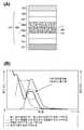
도 1의 (A) 및 도 1의 (B)는 본 발명의 일양태의 개념을 설명하는 도면이다.
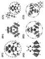
도 2는 본 발명의 일양태에 따른 계산 결과를 나타내는 도면이다.
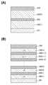
도 3의 (A1), 도 3의 (A2), 도 3의 (B1), 도 3의 (B2), 도 3의 (C1) 및 도 3의 (C2)는 본 발명의 일양태에 따른 계산 결과를 나타내는 도면이다.
도 4는 본 발명의 일양태에 적용하는 여기 착체의 에너지 준위를 설명하는 도면이다.
도 5는 발광 소자의 구조에 대하여 설명하는 도면이다.
도 6의 (A) 및 도 6의 (B)는 발광 소자의 구조에 대하여 설명하는 도면이다.
도 7은 발광 장치에 대하여 설명하는 도면이다.
도 8의 (A) 및 도 8의 (B)는 발광 장치에 대하여 설명하는 도면이다.
도 9의 (A) 내지 도 9의 (D)는 전자 기기에 대하여 설명하는 도면이다.
도 10의 (A) 내지 도 10의 (C)는 전자 기기에 대하여 설명하는 도면이다.
도 11은 조명기구에 대하여 설명하는 도면이다.
도 12는 발광 소자 1의 구조에 대하여 설명하는 도면이다.
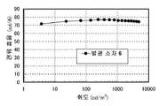
도 13은 발광 소자 1의 전류 밀도-휘도 특성을 나타내는 도면이다.
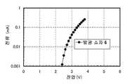
도 14는 발광 소자 1의 전압-휘도 특성을 나타내는 도면이다.
도 15는 발광 소자 1의 휘도-전류 효율 특성을 나타내는 도면이다.
도 16은 발광 소자 1의 전압-전류 특성을 나타내는 도면이다.
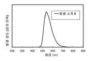
도 17은 발광 소자 1의 발광 스펙트럼을 나타내는 도면이다.
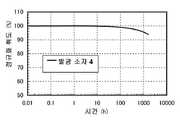
도 18은 발광 소자 1의 신뢰성을 나타내는 도면이다.
도 19는 발광 소자 2의 전류 밀도-휘도 특성을 나타내는 도면이다.
도 20은 발광 소자 2의 전압-휘도 특성을 나타내는 도면이다.
도 21은 발광 소자 2의 휘도-전류 효율 특성을 나타내는 도면이다.
도 22는 발광 소자 2의 전압-전류 특성을 나타내는 도면이다.
도 23은 발광 소자 2의 발광 스펙트럼을 나타내는 도면이다.
도 24는 발광 소자 3의 구조에 대하여 설명하는 도면이다.
도 25는 발광 소자 3의 전류 밀도-휘도 특성을 나타내는 도면이다.
도 26은 발광 소자 3의 전압-휘도 특성을 나타내는 도면이다.
도 27은 발광 소자 3의 휘도-전류 효율 특성을 나타내는 도면이다.
도 28은 발광 소자 3의 전압-전류 특성을 나타내는 도면이다.
도 29는 발광 소자 3의 발광 스펙트럼을 나타내는 도면이다.
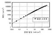
도 30은 발광 소자 4의 전류 밀도-휘도 특성을 나타내는 도면이다.
도 31은 발광 소자 4의 전압-휘도 특성을 나타내는 도면이다.
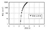
도 32는 발광 소자 4의 휘도-전류 효율 특성을 나타내는 도면이다.
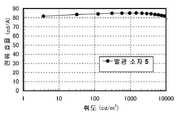
도 33은 발광 소자 4의 전압-전류 특성을 나타내는 도면이다.
도 34는 발광 소자 4의 발광 스펙트럼을 나타내는 도면이다.
도 35는 발광 소자 4의 신뢰성을 나타내는 도면이다.
도 36은 발광 소자 5의 전류 밀도-휘도 특성을 나타내는 도면이다.
도 37은 발광 소자 5의 전압-휘도 특성을 나타내는 도면이다.
도 38은 발광 소자 5의 휘도-전류 효율 특성을 나타내는 도면이다.
도 39는 발광 소자 5의 전압-전류 특성을 나타내는 도면이다.
도 40은 발광 소자 5의 발광 스펙트럼을 나타내는 도면이다.
도 41은 발광 소자 5의 신뢰성을 나타내는 도면이다.
도 42는 발광 소자 6의 전류 밀도-휘도 특성을 나타내는 도면이다.
도 43은 발광 소자 6의 전압-휘도 특성을 나타내는 도면이다.
도 44는 발광 소자 6의 휘도-전류 효율 특성을 나타내는 도면이다.
도 45는 발광 소자 6의 전압-전류 특성을 나타내는 도면이다.
도 46은 발광 소자 6의 발광 스펙트럼을 나타내는 도면이다.
도 47은 발광 소자 6의 신뢰성을 나타내는 도면이다.1 (A) and 1 (B) are diagrams for explaining the concept of one aspect of the present invention.
FIG. 2 is a diagram showing a calculation result according to an embodiment of the present invention. FIG.
Figures 3 (A1), 3 (A2), 3 (B1), 3 (B2), 3 (C1) and 3 (C2) Fig.
4 is a view for explaining the energy level of an excited complex applied to an embodiment of the present invention.
5 is a view for explaining the structure of a light emitting element.
6A and 6B are views for explaining the structure of the light emitting device.
7 is a view for explaining a light emitting device.
8 (A) and 8 (B) are diagrams for explaining the light emitting device.
Figs. 9A to 9D are views for explaining an electronic apparatus. Fig.
10 (A) to 10 (C) are diagrams for explaining an electronic apparatus.
11 is a view for explaining a lighting device.
12 is a view for explaining the structure of the
13 is a graph showing the current density-luminance characteristic of the light-emitting
14 is a graph showing voltage-luminance characteristics of the light-emitting
15 is a graph showing the luminance-current efficiency characteristics of the light-emitting
16 is a diagram showing the voltage-current characteristics of the light-emitting
17 is a diagram showing an emission spectrum of the light-emitting
18 is a view showing the reliability of the light-emitting
19 is a diagram showing the current density-luminance characteristic of the
20 is a diagram showing voltage-luminance characteristics of the light-emitting
21 is a diagram showing luminance-current efficiency characteristics of the light-emitting
22 is a diagram showing voltage-current characteristics of the light-emitting
23 is a diagram showing an emission spectrum of the
Fig. 24 is a view for explaining the structure of the
25 is a diagram showing the current density-luminance characteristic of the
26 is a diagram showing voltage-luminance characteristics of the
27 is a diagram showing luminance-current efficiency characteristics of the light-emitting
28 is a diagram showing voltage-current characteristics of the light-emitting
29 is a diagram showing an emission spectrum of the
30 is a diagram showing the current density-luminance characteristic of the
31 is a diagram showing the voltage-luminance characteristic of the light-emitting
32 is a graph showing luminance-current efficiency characteristics of the light-emitting
33 is a diagram showing the voltage-current characteristics of the light-emitting
34 is a view showing an emission spectrum of the
35 is a view showing the reliability of the
36 is a diagram showing current density-luminance characteristics of the
37 is a diagram showing voltage-luminance characteristics of the
38 is a diagram showing luminance-current efficiency characteristics of the light-emitting
39 is a diagram showing the voltage-current characteristics of the light-emitting
40 is a diagram showing an emission spectrum of the light-emitting
41 is a view showing the reliability of the
42 is a diagram showing the current density-luminance characteristic of the
43 is a graph showing the voltage-luminance characteristic of the light-emitting
44 is a graph showing luminance-current efficiency characteristics of the light-emitting
45 is a diagram showing voltage-current characteristics of the light-emitting
46 is a view showing an emission spectrum of the
Fig. 47 is a diagram showing the reliability of the
이하, 본 발명의 실시형태에 대하여 도면을 이용하여 상세하게 설명한다. 단, 본 발명은 이하의 설명으로 한정되지 않고, 본 발명의 취지 및 그 범위로부터 벗어나는 일 없이 그 형태 및 상세한 사항을 다양하게 변경할 수 있다. 따라서, 본 발명은 이하에 나타내는 실시형태의 기재 내용으로 한정하여 해석되는 것은 아니다.BEST MODE FOR CARRYING OUT THE INVENTION Hereinafter, embodiments of the present invention will be described in detail with reference to the drawings. However, the present invention is not limited to the following description, and various changes may be made in form and detail without departing from the spirit and scope of the present invention. Therefore, the present invention should not be construed as being limited to the contents of the embodiments described below.
(발광 소자에서의 발광의 소과정)(Small process of light emission in the light emitting element)
우선, 인광성 화합물을 게스트 재료로서 이용하는 발광 소자에서의 발광의 일반적인 소과정에 대하여 설명한다. 단, 여기에서는 여기 에너지를 제공하는 측의 분자를 호스트 분자, 여기 에너지를 받는 측의 분자를 게스트 분자라고 한다.First, a general procedure of light emission in a light emitting device using a phosphorescent compound as a guest material will be described. Here, the molecule on the side providing the excitation energy is referred to as a host molecule, and the molecule on the side receiving the excitation energy is referred to as a guest molecule.
(1) 전자 및 정공(홀)이 게스트 분자에서 재결합하고, 게스트 분자가 여기 상태가 되는 경우(직접 재결합 과정).(1) When electrons and holes (holes) recombine in the guest molecules and the guest molecules become excited (direct recombination process).
(1-1) 게스트 분자의 여기 상태가 삼중항 여기 상태일 때, 게스트 분자는 인광을 발한다.(1-1) When the excited state of the guest molecule is triplet excited, the guest molecule emits phosphorescence.
(1-2) 게스트 분자의 여기 상태가 일중항 여기 상태일 때, 일중항 여기 상태의 게스트 분자는 삼중항 여기 상태에 항간 교차하여, 인광을 발한다.(1-2) When the excited state of the guest molecule is a singlet excited state, the singlet excited state guest molecules intersect with the triplet excited state to emit phosphorescence.
즉, 상기 (1)의 직접 재결합 과정에서는 게스트 분자의 항간 교차 효율, 및 인광 양자 수율만 높다면, 높은 발광 효율을 얻을 수 있게 된다. 단, 호스트 분자의 T1 준위는 게스트 분자의 T1 준위보다 높은 것이 바람직하다.That is, in the direct recombination process of (1), if the intersecting cross efficiency of the guest molecules and the phosphorescent quantum yield are high, high luminous efficiency can be obtained. However, T1 level of the host molecule is preferably higher than the T1 level of the guest molecule.
(2) 전자 및 정공(홀)이 호스트 분자에서 재결합하고, 호스트 분자가 여기 상태가 되는 경우(에너지 이동 과정).(2) When electrons and holes (holes) recombine in a host molecule and a host molecule becomes an excited state (energy transfer process).
(2-1) 호스트 분자의 여기 상태가 삼중항 여기 상태일 때, 호스트 분자의 T1 준위가 게스트 분자의 T1 준위보다 높은 경우, 호스트 분자로부터 게스트 분자로 여기 에너지가 이동하고, 게스트 분자가 삼중항 여기 상태가 된다. 삼중항 여기 상태가 된 게스트 분자는 인광을 발한다. 단, 호스트 분자의 T1 준위로부터 게스트 분자의 일중항 여기 에너지의 준위(S1 준위)로의 에너지 이동은 호스트 분자가 인광 발광하지 않는 한 금제이고, 주된 에너지 이동 과정이 되기 어렵기 때문에; 여기에서는 생략한다. 즉, 하기 식 (2-1)과 같이, 호스트 분자의 삼중항 여기 상태(3H*)로부터 게스트 분자의 삼중항 여기 상태(3G*)에의 에너지 이동이 중요하다(식 중, 1G는 게스트 분자의 일중항 기저 상태, 1H는 호스트 분자의 일중항 기저 상태를 나타낸다).(2-1) When the excited state of the host molecule is in the triplet excited state, when the T1 level of the host molecule is higher than the T1 level of the guest molecule, the excitation energy moves from the host molecule to the guest molecule, Triplet excited state. Guest molecules that have become triplet excited state emit phosphorescence. However, the singlet energy level go to (S1 level) of the excitation energy of the guest molecule from T1 level of the host molecule is a molecule that does not illicit a host light-emitting phosphor, it is difficult to be the principal energy transfer process; They are omitted here. That is, as shown in the following formula (2-1), the energy transfer from the triplet excited state (3H* ) of the host molecule to the triplet excited state (3G* ) of the guest molecule is important 1 < / RTI > represents the singlet state basis state, and 1H represents the singlet state basis state of the host molecule).
3H*+1G → 1H+3G* (2-1)3H* + 1G- > 1H + 3G* (2-1)
(2-2) 호스트 분자의 여기 상태가 일중항 여기 상태일 때, 호스트 분자의 S1 준위가 게스트 분자의 S1 준위 및 T1 준위보다 높은 경우, 호스트 분자로부터 게스트 분자로 여기 에너지가 이동하고, 게스트 분자가 일중항 여기 상태 또는 삼중항 여기 상태가 된다. 삼중항 여기 상태가 된 게스트 분자는 인광을 발한다. 또한, 일중항 여기 상태가 된 게스트 분자는 삼중항 여기 상태에 항간 교차하고, 인광을 발한다.(2-2) When the excited state of the host molecule is singlet excited state, when the S1 level of the host molecule is higher than the S1 and T1 levels of the guest molecule, the excitation energy moves from the host molecule to the guest molecule , And the guest molecule becomes singlet excited state or triplet excited state. Guest molecules that have become triplet excited state emit phosphorescence. In addition, the guest molecules in the singlet excited state cross each other to the triplet excited state and emit phosphorescence.
즉, 하기 식 (2-2A)과 같이, 호스트 분자의 일중항 여기 상태(1H*)로부터 게스트 분자의 일중항 여기 상태(1G*)로 에너지 이동하고, 그 후 항간 교차에 의해 게스트 분자의 삼중항 여기 상태(3G*)가 생성하는 과정과, 하기 식 (2-2B)과 같이, 호스트 분자의 일중항 여기 상태(1H*)로부터 게스트 분자의 삼중항 여기 상태(3G*)로 직접 에너지 이동하는 과정을 고려할 수 있다.That is, as shown in the following formula (2-2A), energy is moved from the singlet excited state (1H* ) of the host molecule to the singlet excited state (1G* ) of the guest molecule, (3G* ) from the singlet excited state (1H* ) of the host molecule to the triplet excited state (3G* ) of the guest molecule as shown in the following equation (2-2B) Can be considered.
1H*+1G → 1H+1G* → (항간 교차) → 1H+3G* (2-2A)1H* + 1G- > 1H + 1G* - > (Crosswise intersection) - > 1H + 3G* (2-2A)
1H*+1G → 1H+3G* (2-2B)1H* + 1G- > 1H + 3G* (2-2B)
상기 (2)에서 서술한 모든 에너지 이동 과정이 효율적으로 일어나면, 호스트 분자의 삼중항 여기 에너지 및 일중항 여기 에너지 쌍방이 효율적으로 게스트 분자의 삼중항 여기 상태(3G*)로 변환된다. 따라서, 고효율 발광이 가능해진다. 반대로, 호스트 분자로부터 게스트 분자로 여기 에너지가 이동하기 전에, 호스트 분자 자체가 그 여기 에너지를 광 또는 열로서 방출하여 실활하면, 발광 효율이 저하하게 된다.When all of the energy transfer processes described in (2) above occur efficiently, both triplet excitation energies and singlet excitation energies of the host molecules are efficiently converted to the triplet excitation state (3G* ) of the guest molecule. Therefore, high-efficiency light emission is possible. On the other hand, if the host molecule itself releases the excitation energy as light or heat and inactivates before the excitation energy moves from the host molecule to the guest molecule, the luminous efficiency is lowered.
다음으로, 상술한 호스트 분자와 게스트 분자의 분자 간의 에너지 이동 과정의 지배 인자에 대하여 설명한다. 분자 간의 에너지 이동 기구로서는 이하의 2개의 기구가 제창되고 있다.Next, the dominant factors of the above-described energy transfer process between the host molecule and the guest molecule will be described. As the energy transfer mechanism between molecules, the following two mechanisms are proposed.
우선, 1번째 기구인 펠스터 기구(쌍극자-쌍극자 상호 작용)는 에너지 이동에 분자 간의 직접적 접촉을 필요로 하지 않고, 호스트 분자 및 게스트 분자 간의 쌍극자 진동의 공명 현상을 통하여 에너지 이동이 일어나는 기구이다. 쌍극자 진동의 공명 현상에 의해 호스트 분자가 게스트 분자에 에너지를 제공하고, 호스트 분자가 기저 상태가 되고, 게스트 분자가 여기 상태가 된다. 단, 펠스터 기구의 속도 상수 kh*→g를 수식 (1)에 나타낸다.First, the first mechanism, the Pelter mechanism (dipole-dipole interaction) is a mechanism in which energy transfer takes place through resonance of dipole oscillation between the host molecule and the guest molecule, without requiring direct contact between the molecules for energy transfer. The resonance phenomenon of the dipole oscillation causes the host molecule to provide energy to the guest molecule, the host molecule to become the ground state, and the guest molecule to become the excited state. However, the rate constant kh *? G of the pastel mechanism is expressed by the following equation (1).
[수식 1][Equation 1]

수식 (1)에서 v는 진동수를 나타내고, f'h(v)는 호스트 분자의 규격화된 발광 스펙트럼(일중항 여기 상태로부터의 에너지 이동을 논하는 경우는 형광 스펙트럼, 삼중항 여기 상태로부터의 에너지 이동을 논하는 경우는 인광 스펙트럼)을 나타내고, εg(v)는 게스트 분자의 몰 흡광 계수를 나타내고, N은 아보가드로의 수를 나타내고, n은 매체의 굴절률을 나타내고, R은 호스트 분자와 게스트 분자의 분자 간 거리를 나타내고, τ은 실측되는 여기 상태의 수명(형광 수명이나 인광 수명)을 나타내고, c는 광속을 나타내고, φ은 발광 양자 수율(일중항 여기 상태로부터의 에너지 이동을 논하는 경우는 형광 양자 수율, 삼중항 여기 상태로부터의 에너지 이동을 논하는 경우는 인광 양자 수율)을 나타내고, K2는 호스트 분자와 게스트 분자의 천이 쌍극자 모멘트의 배향을 나타내는 계수(0∼4)이다. 단, 랜덤 배향의 경우는 K2=2/3이다.In the formula (1), v represents the frequency, f 'h (v) represents the normalized luminescence spectrum of the host molecule (fluorescence spectrum when discussing energy transfer from singlet excited state, energy transfer from triplet excited state represents a phosphorescent spectrum) when discussing, εg (v) represents the molar extinction coefficient of the guest molecule, N denotes the Avogadro's number, n denotes a refractive index of the medium, R is a host molecule and the guest molecule (Fluorescence lifetime or phosphorescence lifetime), c represents a light flux, and? Represents a light emission quantum yield (fluorescence when discussing energy transfer from singlet excited state) Quantum yield, the quantum yield of phosphorescence when discussing the energy transfer from the triplet excited state), K2 represents the transient dipole moment of the host molecule and the guest molecule (0 to 4) indicating orientation. However, in the case of random orientation, K2 = 2/3.
다음으로, 2번째 기구인 덱스터 기구(전자 교환 상호 작용)에서는 호스트 분자와 게스트 분자가 궤도의 중첩을 일으키는 접촉 유효 거리에 가까워지고, 여기 상태의 호스트 분자의 전자와 기저 상태의 게스트 분자의 전자의 교환을 통하여 에너지 이동이 일어난다. 단, 덱스터 기구의 속도 상수 kh*→g를 수식 (2)에 나타낸다.Next, in the Dexter mechanism (electron exchange interaction), which is the second mechanism, the host molecule and the guest molecule are close to the contact effective distance causing the overlap of the orbit, and electrons of the excited host molecule and electrons of the guest molecule of the ground state Energy exchange occurs through exchange. However, the rate constant kh* → g of the Dexter mechanism is shown in Equation (2).
[수식 2][Equation 2]

수식 (2)에서, h는 플랑크 상수이고, K'는 에너지 차원을 가지는 상수이고, ν는 진동수를 나타내고, f'h(ν)는 호스트 분자의 규격화된 발광 스펙트럼(일중항 여기 상태로부터의 에너지 이동을 논하는 경우는 형광 스펙트럼, 삼중항 여기 상태로부터의 에너지 이동을 논하는 경우는 인광 스펙트럼)을 나타내고, ε'g(ν)는 게스트 분자의 규격화된 흡수 스펙트럼을 나타내고, L은 실효 분자 반경을 나타내고, R은 호스트 분자와 게스트 분자의 분자 간 거리를 나타낸다.In Equation (2), h is a Planck constant, K 'is a constant having an energy dimension, v is a frequency, f'h (v) is a normalized emission spectrum of the host molecule (energy from singlet excited state Ε 'g (ν) represents the normalized absorption spectrum of the guest molecule, and L represents the effective radius of the molecule (ie, the wavelength of the light emitted from the triplet excited state) , And R represents the intermolecular distance between the host molecule and the guest molecule.
여기서, 호스트 분자로부터 게스트 분자로의 에너지 이동 효율(φET)은 수식 (3)으로 나타내어진다고 생각된다. kr은 호스트 분자의 발광 과정(일중항 여기 상태로부터의 에너지 이동을 논하는 경우는 형광, 삼중항 여기 상태로부터의 에너지 이동을 논하는 경우는 인광)의 속도 상수를 나타내고, kn은 호스트 분자의 비발광 과정(열 실활이나 항간 교차)의 속도 상수를 나타내고, τ은 실측되는 호스트 분자의 여기 상태의 수명을 나타낸다.Here, it is considered that the energy transfer efficiency?ET from the host molecule to the guest molecule is represented by equation (3). kr is the rate constant of the host molecule's emission process (fluorescence when discussing energy transfer from singlet excited state, phosphorescence when discussing energy transfer from triplet excited state), kn is the rate constant of the host molecule (Thermal inactivation or intersecting crossing), and τ represents the lifetime of the excited state of the observed host molecule.
[수식 3][Equation 3]

수식 (3)에 의해, 에너지 이동 효율(φET)을 높게 하기 위해서는 에너지 이동의 속도 상수 kh*→g를 크게 하고, 그외 경합하는 속도 상수 kr+kn(=1/τ)가 상대적으로 작아지면 좋은 것을 알 수 있다.In order to increase the energy transfer efficiency?ET by the equation (3), it is necessary to increase the rate constant kh*? G of the energy transfer and increase the rate constant kr + kn (= 1 /?) If you get smaller, you can see something good.
((2-1)의 에너지 이동 효율)(Energy transfer efficiency of (2-1)
여기서 우선, (2-1)의 에너지 이동 과정을 생각해 본다. 이 경우, 펠스터형(식 (1))은 금제되기 때문에, 덱스터형(식 (2))만 고려하면 좋다. 식 (2)에 의하면, 속도 상수 kh*→g를 크게 하기 위해서는 호스트 분자의 발광 스펙트럼(삼중항 여기 상태로부터의 에너지 이동을 논하고 있으므로 인광 스펙트럼)과 게스트 분자의 흡수 스펙트럼(일중항 기저 상태로부터 삼중항 여기 상태에의 직접 천이에 상당하는 흡수)의 중첩이 큰 것이 좋은 것을 알 수 있다.First, consider the energy transfer process of (2-1). In this case, only the Dexter type (equation (2)) may be considered because the feller type (equation (1)) is not available. According to equation (2), in order to increase the rate constant kh* → g , the emission spectrum of the host molecule (the phosphorescence spectrum is discussed because of the energy transfer from the triplet excited state) and the absorption spectrum of the guest molecule The absorption corresponding to the direct transition to the triplet excited state).
본 발명의 일양태에서는 인광성 화합물을 게스트 재료로서 이용한다. 인광성 화합물의 흡수 스펙트럼에서는 일중항 기저 상태로부터 삼중항 여기 상태에의 직접 천이에 상당하는 흡수가 관측되는 경우가 있고, 이는 가장 장파장측에 나타나는 흡수대이다. 특히 발광성 이리듐 착체에서는 가장 장파장측의 흡수대는 500∼600nm 부근에 광대한 흡수대로서 나타나는 경우가 많다(물론, 발광 파장에 따라서는 보다 단파장측이나 보다 장파장측에 나타나는 경우도 있음). 이 흡수대는 주로 삼중항 MLCT(Metal to Ligand Charge Transfer) 천이에 유래한다. 단, 이 흡수대에는 삼중항 π-π* 천이나 일중항 MLCT 천이에 유래하는 흡수도 일부 포함되고, 이들이 중첩되어, 흡수 스펙트럼의 가장 장파장측에 광대한 흡수대를 형성하고 있다고 생각된다. 즉, 최저 일중항 여기 상태와 최저 삼중항 여기 상태의 차이는 작고, 이들에 유래하는 흡수가 중첩되어, 흡수 스펙트럼의 가장 장파장측에 광대한 흡수대를 형성하고 있다고 생각된다. 따라서, 게스트 재료에, 유기 금속 착체(특히 이리듐 착체)를 이용할 때는 이와 같이 가장 장파장측에 존재하는 광대한 흡수대와, 호스트 재료의 인광 스펙트럼이 크게 중첩됨으로써, 속도 상수 kh*→g를 크게 하고, 에너지 이동 효율을 높일 수 있다.In one embodiment of the present invention, a phosphorescent compound is used as a guest material. In the absorption spectrum of a phosphorescent compound, absorption corresponding to a direct transition from a singlet ground state to a triplet excited state is sometimes observed, which is the absorption band appearing on the longest wavelength side. In particular, in the case of the luminescent iridium complex, the absorption band on the longest wavelength side often appears as an extensive absorption band in the vicinity of 500 to 600 nm (although it may appear on the shorter wavelength side or the longer wavelength side depending on the light emission wavelength). This absorption band mainly comes from the triple-MLCT (Metal to Ligand Charge Transfer) transition. However, it is considered that this absorption band includes a part of the absorption attributable to triplet π-π* cloth or singlet MLCT transition, and these are overlapped to form an extensive absorption band on the longest wavelength side of the absorption spectrum. That is, it is considered that the difference between the lowest singlet excited state and the lowest triplet excited state is small, the absorption derived therefrom is superimposed, and an extensive absorption band is formed on the longest wavelength side of the absorption spectrum. Therefore, when an organometallic complex (especially an iridium complex) is used for the guest material, the large absorption band on the longest wavelength side and the phosphorescence spectrum of the host material are greatly overlapped to increase the rate constant kh* - g , Energy transfer efficiency can be increased.
또한, 통상, 호스트 재료에는 형광성 화합물을 이용하기 때문에; 인광 수명(τ)은 밀리초 이상으로 매우 길다(kr+kn이 작음). 이것은 삼중항 여기 상태로부터 기저 상태(일중항)로의 천이가 금제 천이이기 때문이다. 수식 (3)으로부터, 이것은 에너지 이동 효율(φET)에 대해서 유리하게 작용한다.Further, since a fluorescent compound is generally used for the host material; The phosphorescence lifetime (τ) is very long, more than milliseconds (kr + kn is small). This is because the transition from the triplet excited state to the base state (singlet) is a transitional transition. From equation (3), this works favorably on the energy transfer efficiency, [phi]ET .
이상을 고려하면, 호스트 재료의 삼중항 여기 상태로부터 게스트 재료의 삼중항 여기 상태로의 에너지 이동, 즉 식 (2-1)의 과정은 호스트 재료의 인광 스펙트럼과, 게스트 재료의 일중항 기저 상태로부터 삼중항 여기 상태로의 직접 천이에 상당하는 흡수 스펙트럼을 중첩하기만 하면, 대체로 일어나기 쉬운 경향이 있다.Considering the above, the energy transfer from the triplet excited state of the host material to the triplet excited state of the guest material, that is, the process of Equation (2-1), is obtained from the phosphorescence spectrum of the host material and the singlet ground state of the guest material The absorption spectrum corresponding to the direct transition to the triplet excited state tends to occur in general.
((2-2)의 에너지 이동 효율)(Energy transfer efficiency of (2-2)
다음으로, (2-2)의 에너지 이동 과정을 생각해 본다. 식 (2-2A)의 과정은 게스트 재료의 항간 교차 효율의 영향을 받는다. 따라서, 극한까지 발광 효율을 높이기 위해서는 식 (2-2B)의 과정이 중요하게 생각된다. 이 경우, 덱스터형(식 (2))은 금제가 되기 때문에, 펠스터형(식 (1))만을 생각하면 좋다.Next, consider the energy transfer process of (2-2). The process of Eq. (2-2A) is affected by the inter-crossover efficiency of the guest material. Therefore, the process of Equation (2-2B) is considered to be important for increasing the luminous efficiency up to the limit. In this case, the Dexter type (Eq. (2)) is forbidden. Therefore, only the Feldster type (Eq.
식 (1)과 식 (3)으로부터 τ을 소거하면, 에너지 이동 효율(φET)은 양자 수율(φ)(일중항 여기 상태로부터의 에너지 이동을 논하고 있으므로, 형광 양자 수율)이 높은 것이 좋다고 할 수 있다. 그러나 실제는 또한, 중요한 팩터로서 호스트 분자의 발광 스펙트럼(일중항 여기 상태로부터의 에너지 이동을 논하고 있으므로 형광 스펙트럼)과 게스트 분자의 흡수 스펙트럼(일중항 기저 상태로부터 삼중항 여기 상태로의 직접 천이에 상당하는 흡수)의 중첩이 큰 것도 필요하다(또한, 게스트 분자의 몰 흡광 계수도 높은 것이 바람직함). 이것은 호스트 재료의 형광 스펙트럼과 게스트 재료인 인광성 화합물의 가장 장파장측에 나타나는 흡수대가 중첩되는 것을 의미한다.From the equations (1) and (3), it can be said that the energy transfer efficiency?ET is preferably high because of the quantum yield? (Energy transfer from singlet excited state is discussed, . However, in practice, it is also important that the luminescence spectrum of the host molecule (the fluorescence spectrum because it is discussing the energy transfer from the singlet excited state) and the absorption spectrum of the guest molecule (equivalent to the direct transition from the singlet ground state to the triplet excited state) (Also, it is preferable that the molar extinction coefficient of the guest molecule is also high). This means that the fluorescence spectrum of the host material overlaps with the absorption band appearing on the longest wavelength side of the phosphorescent compound as the guest material.
그러나, 이를 실현하는 것은 종래에는 매우 곤란했다. 왜냐하면, 상술한 (2-1)의 과정과 (2-2)의 과정 모두를 효율적으로 행하려고 하면, 상술한 논의로부터, 호스트 재료의 인광 스펙트럼뿐만 아니라, 형광 스펙트럼도 게스트 재료의 가장 장파장측의 흡수대와 중첩되도록 설계해야 하기 때문이다. 다시 말하면, 호스트 재료의 형광 스펙트럼이 인광 스펙트럼과 같은 위치에 오도록 호스트 재료를 설계해야 하는 것이다.However, it has been very difficult in the past to realize this. If both of the processes (2-1) and (2-2) described above are to be carried out efficiently, not only the phosphorescence spectrum of the host material but also the fluorescence spectrum of the host material Because it must be designed to overlap with the absorption band. In other words, the host material must be designed such that the fluorescence spectrum of the host material is in the same position as the phosphorescence spectrum.
그런데, 일반적으로 S1 준위와 T1 준위는 크게 다르기(S1 준위>T1 준위) 때문에; 형광 발광 파장과 인광 발광 파장도 크게 다르다(형광 발광 파장<인광 발광 파장). 예를 들면, 인광성 화합물을 포함한 발광 소자에서, 호스트 재료로서 자주 이용되는 4,4'-다이(N-카바졸릴)바이페닐(약칭:CBP)은 500nm 부근에 인광 스펙트럼을 가지지만, 한편 형광 스펙트럼은 400nm 부근이고, 100nm의 간격이 있다. 이 예로부터 생각해 보아도, 호스트 재료의 형광 스펙트럼이 인광 스펙트럼과 같은 위치에 오도록 호스트 재료를 설계하는 것은 매우 어렵다. 따라서, 호스트 재료의 일중항 여기 상태로부터의 게스트 재료로의 에너지 이동 효율의 향상은 매우 중요하다.However, since the S1 level and the T1 level are generally different (S1 level> T1 level) in general; The fluorescence emission wavelength and the phosphorescence emission wavelength also differ greatly (fluorescence emission wavelength <phosphorescence emission wavelength). For example, in a light-emitting device including a phosphorescent compound, 4,4'-di (N-carbazolyl) biphenyl (abbreviation: CBP) often used as a host material has a phosphorescence spectrum near 500 nm, The spectrum is around 400 nm, with an interval of 100 nm. From this example, it is very difficult to design the host material such that the fluorescence spectrum of the host material is in the same position as the phosphorescence spectrum. Therefore, it is very important to improve the energy transfer efficiency from the singlet excited state of the host material to the guest material.
따라서, 본 발명의 일양태는 이러한 호스트 재료의 일중항 여기 상태로부터 게스트 재료로의 에너지 이동 효율에 관한 문제점을 극복할 수 있는 유용한 방법을 제공하는 것이다. 이하에, 그 구체적인 양태를 설명한다.Thus, one aspect of the present invention is to provide a useful method that can overcome the problems with energy transfer efficiency from the singlet excited state of such a host material to the guest material. Hereinafter, specific embodiments thereof will be described.
(실시형태 1)(Embodiment 1)
본 실시형태에서는 본 발명의 일양태인 발광 소자를 구성하는데 있어서의 개념 및 구체적인 발광 소자의 구성에 대하여 설명한다. 단, 본 발명의 일양태인 발광 소자는 한쌍의 전극 간에 제공된 발광층을 포함하는 EL층을 사이에 끼워 형성되어 있고, 발광층은 인광성 화합물인 게스트 재료와, 제 1 유기 화합물과 제 2 유기 화합물을 포함하여 형성된다.In the present embodiment, the concept of constituting the light emitting element of the present invention and the specific configuration of the light emitting element will be described. However, the light-emitting element of the present invention is formed by sandwiching the EL layer including a light-emitting layer provided between a pair of electrodes, and the light-emitting layer includes a guest material as a phosphorescent compound and a first organic compound and a second organic compound .
우선, 본 발명의 일례인 발광 소자의 소자 구조에 대하여, 도 1의 (A)에 의해 설명한다.First, a device structure of a light emitting device, which is an example of the present invention, will be described with reference to FIG. 1A.
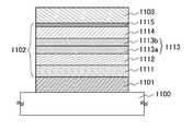
도 1의 (A)에 나타내는 소자 구조는 한쌍의 전극(양극(101), 음극(102)) 간에 제공된 발광층(106)을 포함하는 EL층(103)이 끼워져 있고, EL층(103)은 양극(101)측으로부터 정공(홀) 주입층(104), 정공(홀) 수송층(105), 발광층(106)(106a, 106b), 전자 수송층(107), 전자 주입층(108) 등이 순차로 적층된 구조를 가진다.1 (A), an
본 발명의 일양태에서의 발광층(106)은 도 1의 (A)에 나타내는 바와 같이 게스트 재료인 인광성 화합물(109)과, 제 1 유기 화합물(110)과, 제 2 유기 화합물(111)을 포함하는 층이다. 제 1 유기 화합물(110)로서는 주로 10-6cm2/Vs 이상의 전자 이동도를 가지는 전자 수송성 재료를 이용하고, 제 2 유기 화합물(111)로서는 주로 10-6cm2/Vs 이상의 정공 이동도를 가지는 정공(홀) 수송성 재료를 이용한다. 본 명세서 중에서는 제 1 유기 화합물(110)을 호스트 재료라고 칭하고, 제 2 유기 화합물(111)을 어시스트 재료라고 칭하는 것으로 한다.1 (A), a
단, 상기 구성에서, 제 1 유기 화합물(호스트 재료)(110) 및 제 2 유기 화합물(어시스트 재료)(111)의 각각의 삼중항 여기 에너지의 준위(T1 준위)는 인광성 화합물(게스트 재료)(109)의 T1 준위보다 높은 것이 바람직하다. 제 1 유기 화합물(110)(또는 제 2 유기 화합물(111))의 T1 준위가 인광성 화합물(109)의 T1 준위보다 낮으면 발광에 기여하는 인광성 화합물(109)의 삼중항 여기 에너지를 제 1 유기 화합물(110)(또는 제 2 유기 화합물(111))이 소광(퀀치)되고, 발광 효율의 저하를 초래하기 때문이다.However, in the above configuration, the level (T1 level) of the triplet excitation energy of each of the first organic compound (host material) 110 and the second organic compound (assist material) 111 is higher than that of the phosphorescent compound ) is preferably higher than the T1 level of 109. When the T1 level of the first organic compound 110 (or the second organic compound 111) is lower than the T1 level of the
본 발명의 일양태에서의 발광층(106)은 발광층(106) 안에 포함되는 제 2 유기 화합물(어시스트 재료)(111)의 비율이 다른 발광층이 적층된 구조인 것을 특징으로 한다. 구체적으로는 도 1의 (A)에 나타내는 바와 같이, 발광층(106)이 제 1 발광층(106a)과 제 2 발광층(106b)의 적층 구조이고, 제 1 발광층(106a)에서 제 2 유기 화합물(어시스트 재료)(111)이 포함되는 비율은 제 2 발광층(106b)에서 제 2 유기 화합물(어시스트 재료)(111)이 포함되는 비율보다 많은 것을 특징으로 한다.The
또한, 발광층(106)을 구성하는 제 1 발광층(106a) 및 제 2 발광층(106b)의 각각에 관하여, 제 1 유기 화합물(호스트 재료)(110) 및 제 2 유기 화합물(어시스트 재료)(111)이 포함되는 비율에 대해서는 어느 쪽이 많아도 좋고, 본 발명에서는 두 경우 모두 포함하는 것으로 한다.The first organic compound (host material) 110 and the second organic compound (assist material) 111 are used for each of the first
단, 상기 구조의 제 1 발광층(106a)에서, 정공(홀) 수송성 재료인 제 2 유기 화합물(어시스트 재료)(111)의 비율이 적으면, 발광 영역이 제 1 발광층(106a)의 양극측(정공 수송층(105)측)에 치우치게 된다. 한편, 제 1 발광층(106a), 제 2 발광층(106b) 쌍방에서의 제 2 유기 화합물(어시스트 재료)(111)이 너무 많아지면, 캐리어(정공, 전자 모두)가 발광층(106)을 관통하기 쉬워지게 되고, 재결합 효율이 저하되게 된다. 그러나, 도 1의 (A)에서 서술한 본 발명의 일양태의 구성으로 함으로써, 제 1 발광층(106a)의 정공 수송성은 제 2 발광층(106b)의 정공 수송성에 비해 상대적으로 높아지고, 전자 수송성은 그 반대가 된다. 따라서, 여기자는 제 1 발광층(106a)과 제 2 발광층(106b)의 계면을 중심으로 치우치는 일 없이, 또한, 발광층(106) 내로부터 벗어나는 일 없이 분포시킬 수 있다. 그 결과, 발광층(106) 내부에서의 여기자의 편향을 막을 수 있고, 여기자의 밀도가 높아지는 것에 의한 발광층(106)의 열화를 방지할 수 있다. 또한, 발광층(106)으로부터 캐리어가 관통하는 것을 막을 수 있기 때문에, 발광 효율을 높게 유지할 수 있다.When the ratio of the second organic compound (assist material) 111, which is a hole-transporting material, in the first
여기서, 상기 제 1 발광층(106a) 및 제 2 발광층(106b) 중 어느 하나에서도 제 1 유기 화합물(호스트 재료)(110)과 제 2 유기 화합물(어시스트 재료)(111)은 여기 착체(exciplex:엑시플렉스라고도 함)를 형성하는 조합인 것을 특징으로 한다. 또한, 형성된 여기 착체의 발광 파장은 제 1 유기 화합물(호스트 재료)(110)과 제 2 유기 화합물(어시스트 재료)(111)의 각각의 발광 파장(형광 파장)에 비해, 장파장측에 존재한다. 따라서, 제 1 유기 화합물(호스트 재료)(110)의 형광 스펙트럼이나 제 2 유기 화합물(어시스트 재료)(111)의 형광 스펙트럼을 보다 장파장측에 위치하는 발광 스펙트럼으로 변환할 수 있다.Herein, the first organic compound (host material) 110 and the second organic compound (assist material) 111 are excited by excitation in any one of the first
이것은 도 1의 (B)에 나타내는 바와 같이 제 1 유기 화합물(110)(또는 제 2 유기 화합물(111))의 형광 스펙트럼이 비록 인광성 화합물(게스트 재료)(109)의 가장 장파장측에 위치하는 흡수대에 비해 단파장 측에 위치하고, 인광성 화합물(게스트 재료)(109)의 가장 장파장측에 위치하는 흡수대와의 중첩이 없다고 해도, 여기 착체를 형성함으로써, 그 중첩을 크게 할 수 있는 것을 의미한다. 이것에 의해, 상술한 식 (2-2B)의 에너지 이동 효율을 높일 수 있다.This is because the fluorescence spectrum of the first organic compound 110 (or the second organic compound 111) is located on the longest wavelength side of the phosphorescent compound (guest material) 109 as shown in Fig. 1 (B) It means that the superposition can be made large by forming an excited complex even if there is no overlap with the absorption band located on the shorter wavelength side than the absorption band and located on the longest wavelength side of the phosphorescent compound (guest material) 109. As a result, the energy transfer efficiency of the above formula (2-2B) can be increased.
또한, 여기 착체는 일중항 여기 에너지와 삼중항 여기 에너지의 차이가 매우 작다고 생각된다. 다시 말하면, 여기 착체의 일중항 상태로부터의 발광 스펙트럼과 삼중항 상태로부터의 발광 스펙트럼은 매우 근접하게 된다. 따라서, 상술한 바와 같이 여기 착체의 발광 스펙트럼(일반적으로는 여기 착체의 일중항 상태로부터의 발광 스펙트럼)을 인광성 화합물의 가장 장파장측에 위치하는 흡수대에 중첩되도록 설계한 경우, 여기 착체의 삼중항 상태로부터의 발광 스펙트럼(상온에서는 관측되지 않고, 저온에서도 관측되지 않는 경우가 많음)도, 인광성 화합물의 가장 장파장측에 위치하는 흡수대와 중첩되게 된다. 즉, 일중항 여기 상태로부터의 에너지 이동((2-2))뿐만 아니라 삼중항 여기 상태로부터의 에너지 이동((2-1))의 효율도 높아지고, 결과적으로 일중항·삼중항 쌍방을 효율적으로 발광으로 변환할 수 있다.Further, it is considered that the excited complex has a very small difference between singlet excitation energy and triplet excitation energy. In other words, the luminescence spectrum from the singlet state of the excited complex and the luminescent spectrum from the triplet state become very close. Therefore, when the luminescence spectrum of the excited complex (generally, the luminescence spectrum from the singlet state of the excited complex) is designed to be superposed on the absorption band located on the longest wavelength side of the phosphorescent compound as described above, The light emission spectrum from the state (not observed at room temperature and often not observed at low temperature) is superimposed on the absorption band located on the longest wavelength side of the phosphorescent compound. That is, not only the energy transfer from the singlet excited state ((2-2)) but also the efficiency of the energy transfer ((2-1)) from the triplet excited state is increased and consequently both singlet and triplet It can be converted into light emission.
그러므로, 실제로 여기 착체가 이러한 특성을 가지고 있는지에 관하여, 이하에서는 분자 궤도 계산을 이용하여 검증했다. 일반적으로, 복소 방향족 화합물과 방향족 아민의 조합은 방향족 아민의 최저 공분자 궤도(LUMO:Lowest Unoccupied Molecular Orbital) 준위에 비해 깊은 복소 방향족 화합물의 LUMO 준위(전자가 들어가기 쉬운 성질)와 복소 방향족 화합물의 최고 피점유 궤도(HOMO:Highest Occupied Molecular Orbital) 준위에 비해 얕은 방향족 아민의 HOMO 준위(홀이 들어가기 쉬운 성질)의 영향으로, 여기 착체를 형성하는 경우가 많다. 그러므로, 본 발명의 일양태에서의 제 1 유기 화합물(110)의 모델로서 복소 방향족 화합물의 LUMO를 형성하는 대표적인 골격의 다이벤조[f,h]퀴녹살린(약칭:DBq)을 이용하고, 본 발명의 일양태에서의 제 2 유기 화합물(111)의 모델로서 방향족 아민의 HOMO를 형성하는 대표적인 골격의 트라이페닐아민(약칭:TPA)을 이용하고, 이들을 조합하여 계산을 행하였다.Therefore, as to whether the excited complex actually has such a characteristic, the molecular orbital calculation was used to verify the following. In general, the combination of a heteroaromatic compound and an aromatic amine is a combination of a LUMO level of a complex aromatic compound (an electron is likely to enter) and a peak of a heteroaromatic compound, which are deep compared to the lowest unoccupied molecular orbital (LUMO) An excited complex is often formed due to the influence of the HOMO level of the shallow aromatic amine (property likely to enter the hole) as compared with the HOMO (Highest Occupied Molecular Orbital) level. Therefore, as a model of the first
우선, DBq(약칭) 1분자와 TPA(약칭) 1분자의 최저 여기 일중항 상태(S1)와 최저 여기 삼중항 상태(T1)에서의 최적 분자 구조 및 여기 에너지를 시간 의존 밀도 범함수법(TD-DFT)을 이용하여 계산했다. 또한, DBq(약칭)와 TPA(약칭)의 이량체에 대해서도 여기 에너지를 계산했다.First, the optimal molecular structure and excitation energy at the lowest excited state (S1 ) and the lowest excited triplet state (T1 ) of one molecule of DBq (abbreviation) and one molecule of TPA (abbreviation) TD-DFT). Excitation energy was also calculated for dimers of DBq (abbreviated) and TPA (abbreviated).
DFT(밀도 범함수법)의 전에너지(total energy)는 포텐셜 에너지, 전자 간 정전 에너지, 전자의 운동 에너지, 및, 복잡한 전자 간의 상호 작용을 모두 포함하는 교환 상관 에너지의 합으로 나타내어진다. DFT에서는 교환 상관 상호 작용은 전자 밀도로 표현된 1 전자 포텐셜의 범함수(함수의 함수라는 뜻)와 유사하기 때문에, 계산은 고속이고 고정밀도이다. 여기에서는 혼합 범함수인 B3LYP를 이용하여, 교환과 상관 에너지에 따른 각 파라미터의 중량을 규정했다.The total energy of the DFT is expressed as the sum of the potential energy, the interelectrostatic charge energy, the kinetic energy of the electron, and the exchange correlation energy including both interactions between complex electrons. In DFT, the exchange correlation is similar to the function of one electron potential (denoted as a function of the function) expressed in electron density, so that the calculation is fast and highly accurate. Here, we use B3LYP, a mixed function, to define the weight of each parameter with respect to exchange and correlation energy.
또한, 기저 함수로서 6-311(각각의 원자가 궤도에 3개의 단축 함수를 이용한 triple split valence 기저계의 기저 함수)를 모든 원자에 적용했다.We also applied 6-311 as a basis function (the basis function of the triple split valence basis system using three shortening functions for each atom's orbital) to all the atoms.
상술한 기저 함수에 의해, 예를 들면, 수소 원자이면 1s∼3s의 궤도가 고려되고, 또한, 탄소 원자이면 1s∼4s, 2p∼4p의 궤도가 고려되게 된다. 또한, 계산 정밀도 향상을 위하여 분극 기저계로서 수소 원자에는 p함수를, 수소 원자 이외에는 d함수를 더했다.For example, if the base function is a hydrogen atom, the orbit of 1s to 3s is considered, and if it is a carbon atom, the orbit of 1s to 4s and 2p to 4p is considered. In order to improve the calculation accuracy, the p-function is added to the hydrogen atom and the d-function to the hydrogen atom other than the hydrogen atom.
단, 양자 화학 계산 프로그램으로서는 Gaussian 09를 사용했다. 계산은 하이 퍼포먼스 컴퓨터(SGI Japan, Ltd., Altix4700)를 이용하여 행하였다.However, Gaussian 09 was used as a quantum chemistry calculation program. The calculation was performed using a high-performance computer (SGI Japan, Ltd., Altix 4700).
우선, DBq(약칭) 1분자, TPA(약칭) 1분자, 및 DBq(약칭)와 TPA(약칭)의 이량체에 관하여, HOMO 준위 및 LUMO 준위를 산출했다. HOMO 준위 및 LUMO 준위를 도 2에, HOMO 및 LUMO의 분포를 도 3의 (A1), 도 3의 (A2), 도 3의 (B1), 도 3의 (B2), 도 3의 (C1), 및 도 3의 (C2)에, 각각 나타낸다.First, HOMO and LUMO levels were calculated with respect to a dimer of one DBq (abbreviation) molecule, one TPA (abbreviation) molecule, and DBq (abbreviation) and TPA (abbreviation). The HOMO level and the LUMO level are shown in Fig. 2, the distributions of HOMO and LUMO are shown in (A1), (A2), (B1), (B2) , And Fig. 3 (C2), respectively.
도 3의 (A1)에 DBq(약칭) 1분자의 LUMO의 분포를 나타내고; 도 3의 (A2)에 DBq(약칭) 1분자의 HOMO의 분포를 나타내고; 도 3의 (B1)에 TPA(약칭) 1분자의 LUMO의 분포를 나타내고; 도 3의 (B2)에 TPA(약칭) 1분자의 HOMO의 분포를 나타내고; 도 3(C1)에 DBq(약칭)와 TPA(약칭)의 이량체의 LUMO의 분포를 나타내고; 도 3(C2)에 DBq(약칭)와 TPA(약칭)의 이량체의 HOMO의 분포를 나타낸다.FIG. 3 (A1) shows the distribution of LUMO of one molecule of DBq (abbreviated); FIG. 3 (A2) shows the distribution of HOMO of one molecule of DBq (abbreviation); Figure 3 (B1) shows the distribution of LUMO of one molecule of TPA (abbreviated); FIG. 3 (B2) shows the distribution of HOMO of one molecule of TPA (abbreviation); FIG. 3 (C1) shows the distribution of LUMO of a dimer of DBq (abbreviation) and TPA (abbreviation); Figure 3 (C2) shows the HOMO distribution of the dimer of DBq (abbreviation) and TPA (abbreviation).
도 2에 나타내는 바와 같이, DBq(약칭)와 TPA(약칭)의 이량체는 TPA(약칭)의 LUMO 준위에 비해 깊은(낮은) DBq(약칭)의 LUMO 준위(-1.99eV)와, DBq의 HOMO 준위에 비해 얕은(높은) TPA(약칭)의 HOMO 준위(-5.21eV)의 영향으로, DBq(약칭)와 TPA(약칭)의 여기 착체를 형성하는 것이 시사된다. 실제로 도 3의 (C1) 및 도 3의 (C2)로부터 알 수 있는 바와 같이, DBq(약칭)와 TPA(약칭)의 이량체의 LUMO는 DBq(약칭)측에, HOMO는 TPA(약칭)측에 분포되어 있다.As shown in Fig. 2, the dimer of DBq (abbreviation) and TPA (abbreviation) has a LUMO level (-1.99 eV) of DBq (abbreviation) which is deeper (lower) than the LUMO level of TPA It is suggested that an excited complex of DBq (abbreviation) and TPA (abbreviation) is formed due to the influence of the HOMO level (-5.21 eV) of shallow (high) TPA (abbreviation) Actually, as can be seen from FIG. 3 (C1) and FIG. 3 (C2), the LUMO of dimer of DBq (abbreviation) and TPA (abbreviation) is on DBq (abbreviation) side, HOMO is on TPA .
다음으로, DBq(약칭) 1분자의 S1 준위와 T1 준위에서의 최적 분자 구조로부터 얻어진 여기 에너지를 나타낸다. 여기서, S1 준위와 T1 준위의 여기 에너지는 DBq(약칭) 1분자가 발하는 형광과 인광의 파장에 각각 상당한다. DBq(약칭) 1분자의 S1 준위의 여기 에너지는 3.294eV이고, 형광 파장은 376.4nm였다. DBq(약칭) 1분자의 T1 준위의 여기 에너지는 2.460eV이고, 인광 파장은 504.1nm였다.Next, the excitation energy obtained from the optimum molecular structure at the S1 and T1 levels of one DBq (abbreviation) molecule is shown. Here, the excitation energy of the S1 and T1 levels corresponds to the wavelength of fluorescence and phosphorescence emitted by one molecule of DBq (abbreviation), respectively. The excitation energy of the S1 level of one molecule of DBq (abbreviated) was 3.294 eV and the fluorescence wavelength was 376.4 nm. The excitation energy at the T1 level of one DBq (abbreviated) molecule was 2.460 eV and the phosphorescence wavelength was 504.1 nm.
또한, TPA(약칭) 1분자의 S1 준위와 T1 준위에서의 최적 분자 구조로부터 얻어진 여기 에너지를 나타낸다. 여기서, S1 준위와 T1 준위의 여기 에너지는 TPA(약칭) 1분자가 발하는 형광과 인광의 파장에 각각 상당한다. TPA(약칭) 1분자의 S1 준위의 여기 에너지는 3.508eV이고, 형광 파장은 353.4nm였다. TPA(약칭) 1분자의 T1 준위의 여기 에너지는 2.610eV이고, 인광 파장은 474.7nm였다.It also shows the excitation energy obtained from the optimal molecular structure at the S1 and T1 levels of one molecule of TPA (abbr.). Here, the excitation energy of the S1 and T1 levels corresponds to the wavelength of fluorescence and phosphorescence emitted by one molecule of TPA (abbreviation), respectively. The excitation energy of the S1 level of one molecule of TPA (abbr.) Was 3.508 eV, and the fluorescence wavelength was 353.4 nm. The excitation energy at the T1 level of one molecule of TPA (abbr.) Was 2.610 eV and the phosphorescence wavelength was 474.7 nm.
또한, DBq(약칭)와 TPA(약칭)의 이량체의 S1 준위와 T1 준위에서의 최적 분자 구조로부터 얻어진 여기 에너지를 나타낸다. S1 준위와 T1 준위의 여기 에너지는 DBq(약칭)와 TPA(약칭)의 이량체가 발하는 형광과 인광의 파장에 각각 상당한다. DBq(약칭)와 TPA(약칭)의 이량체의 S1 준위의 여기 에너지는 2.036eV이고, 형광 파장은 609.1nm였다. DBq(약칭)와 TPA(약칭)의 이량체의 T1 준위의 여기 에너지는 2.030eV이고, 인광 파장은 610.0nm였다.It also shows the excitation energy obtained from the optimum molecular structure at the S1 and T1 levels of dimers of DBq (abbreviated) and TPA (abbreviated). The excitation energy of the S1 and T1 levels corresponds to the wavelengths of fluorescence and phosphorescence emitted by the dimer of DBq (abbreviation) and TPA (abbreviation), respectively. The excitation energy at the S1 level of the dimer of DBq (abbr.) And TPA (abbreviated name) was 2.036 eV and the fluorescence wavelength was 609.1 nm. The excitation energy of the T1 level of the dimer of DBq (abbr.) And TPA (abbreviated name) was 2.030 eV and the phosphorescence wavelength was 610.0 nm.
이상으로부터, DBq(약칭) 1분자, TPA(약칭) 1분자 중 어느 쪽에서도, 인광 파장이 100nm 가까이 장파장 시프트하고 있는 것을 알 수 있다. 이것은 상술한 CBP(약칭)(실측치)와 같은 경향이고, 계산의 타당성을 지지하는 결과이다.From the above, it can be seen that the phosphorescence wavelength is shifted by about 100 nm in long wavelength in either DBq (abbreviated) molecule or TPA (abbreviated) molecule. This is the same tendency as the above-mentioned CBP (abbreviated name) (actual value), and supports the validity of the calculation.
한편, DBq(약칭)와 TPA(약칭)의 이량체의 형광 파장은 DBq(약칭) 1분자나 TPA(약칭) 1분자의 형광 파장에 비해, 보다 장파장측에 존재하는 것을 알 수 있다. DBq(약칭)와 TPA(약칭)의 이량체의 형광 파장과 인광 파장의 차이는 불과 0.9nm이고, 거의 같은 파장인 것을 알 수 있다.On the other hand, it can be seen that the fluorescence wavelength of the dimer of DBq (abbr.) And TPA (abbreviated name) exists on the longer wavelength side compared with the fluorescence wavelength of one DBq (abbreviation) molecule or TPA (abbreviation) molecule. The difference between the fluorescence wavelength and the phosphorescence wavelength of the dimer of DBq (abbreviated name) and TPA (abbreviated name) is only 0.9 nm, which is almost the same wavelength.
이 결과로부터, 여기 착체는 일중항 여기 에너지와 삼중항 여기 에너지를 거의 같은 에너지에 집약할 수 있다고 할 수 있다. 따라서, 상술한 것처럼, 여기 착체는 그 일중항 상태, 및 삼중항 상태 모두으로부터, 인광성 화합물에 대해서 효율적으로 에너지 이동할 수 있는 것이 시사되었다.From this result, it can be said that the excited complex can concentrate singlet excitation energy and triplet excitation energy to almost the same energy. Thus, as described above, it has been suggested that the excited complex can efficiently transfer energy from the singlet state and the triplet state to the phosphorescent compound.
이와 같이, 본 발명의 일양태인 발광 소자는 발광층에서 형성된 여기 착체의 발광 스펙트럼과 인광성 화합물(게스트 재료)의 흡수 스펙트럼의 중첩을 이용하고, 에너지 이동을 하기 때문에 에너지 이동 효율이 높다. 따라서, 외부 양자 효율이 높은 발광 소자를 실현할 수 있다.As described above, the light emitting device of the present invention has a high energy transfer efficiency because it uses the overlapping of the luminescence spectrum of the excited complex formed in the light emitting layer and the absorption spectrum of the phosphorescent compound (guest material). Therefore, a light emitting device having high external quantum efficiency can be realized.
또한, 여기 착체는 여기 상태에서만 존재하기 때문에, 에너지를 흡수할 수 있는 기저 상태가 존재하지 않는다. 따라서, 인광성 화합물(게스트 재료)의 일중항 여기 상태 및 삼중항 여기 상태로부터 여기 착체로의 에너지 이동에 의해 인광성 화합물(게스트 재료)(109)이 발광하기 전에 실활한다(즉 발광 효율을 잃는다)는 현상은 원리적으로 생기지 않는다고 생각된다. 이것도, 외부 양자 효율을 높일 수 있는 한 요인이다.Further, since the excited complex exists only in the excited state, there is no base state capable of absorbing the energy. Therefore, the phosphorescent compound (guest material) 109 is deactivated (that is, luminescence efficiency is lost) by the energy transfer from the singly excited state of the phosphorescent compound (guest material) to the excited complex from the triplet excited state ), It is considered that the phenomenon does not occur in principle. This is also one factor that can increase the external quantum efficiency.
단, 상술한 여기 착체는 여기 상태에서의 이종 분자 간의 상호 작용에 의해 형성된다. 여기 착체는 비교적 깊은 LUMO 준위를 가지는 재료와, 얕은 HOMO 준위를 가지는 재료의 사이에서 형성하기 쉬운 것이 일반적으로 알려져 있다.However, the above-mentioned excited complexes are formed by the interaction between the dissimilar molecules in the excited state. It is generally known that the complex is easy to form between a material having a relatively deep LUMO level and a material having a shallow HOMO level.
여기 착체의 발광 파장은 HOMO 준위와 LUMO 준위 간의 에너지 차이에 의존한다. 대략적인 경향으로서 에너지 차이가 크면 발광 파장은 짧아지고, 에너지 차이가 작으면 발광 파장은 길어진다.The emission wavelength of the excitation complex depends on the energy difference between the HOMO level and the LUMO level. As a rough tendency, when the energy difference is large, the emission wavelength becomes short, and when the energy difference is small, the emission wavelength becomes long.
따라서, 본 실시형태에서의 제 1 유기 화합물(호스트 재료)(110)과 제 2 유기 화합물(어시스트 재료)(111)의 HOMO 준위 및 LUMO 준위는 각각 다르다. 구체적으로는 제 1 유기 화합물(110)의 HOMO 준위<제 2 유기 화합물(111)의 HOMO 준위<제 1 유기 화합물(110)의 LUMO 준위<제 2 유기 화합물(111)의 LUMO 준위의 순서로 에너지 준위가 다르다(도 4 참조).Therefore, the HOMO and LUMO levels of the first organic compound (host material) 110 and the second organic compound (assist material) 111 in the present embodiment are different from each other. Specifically, the HOMO level of the first
그리고, 이 2개의 유기 화합물에 의해 여기 착체가 형성된 경우, 여기 착체의 LUMO 준위는 제 1 유기 화합물(호스트 재료)(110)에 유래하고, HOMO 준위는 제 2 유기 화합물(어시스트 재료)(111)에 유래한다(도 4 참조). 따라서, 여기 착체의 에너지 차이는 제 1 유기 화합물(호스트 재료)(110)의 에너지 차이, 및 제 2 유기 화합물(어시스트 재료)(111)의 에너지 차이보다 작아진다. 즉, 제 1 유기 화합물(호스트 재료)(110)과 제 2 유기 화합물(어시스트 재료)(111) 각각의 발광 파장에 비해, 여기 착체의 발광 파장은 장파장이 된다.When the excited complex is formed by these two organic compounds, the LUMO level of the excited complex is derived from the first organic compound (host material) 110, and the HOMO level is derived from the second organic compound (assist material) (See Fig. 4). Therefore, the energy difference of the excited complex becomes smaller than the energy difference of the first organic compound (host material) 110 and the energy difference of the second organic compound (assist material) 111. That is, the emission wavelength of the excited complex is longer than the emission wavelength of each of the first organic compound (host material) 110 and the second organic compound (assist material) 111.
단, 본 발명의 일양태에서의 여기 착체의 형성 과정에는 이하의 2개의 과정을 생각할 수 있다.However, in the process of forming an excited complex in one embodiment of the present invention, the following two processes can be considered.
첫 번째 형성 과정은 제 1 유기 화합물(호스트 재료) 및 제 2 유기 화합물(어시스트 재료)이 캐리어를 가진 상태(양이온 또는 음이온)로부터, 여기 착체를 형성하는 형성 과정이다.The first forming process is a forming process in which the first organic compound (host material) and the second organic compound (assist material) form an excited complex from a state (carrier or anion) having a carrier.
일반적으로는 전자 및 정공(홀)이 호스트 재료 중에서 재결합한 경우, 여기 상태의 호스트 재료로부터 게스트 재료로 여기 에너지가 이동하고, 게스트 재료가 여기 상태에 도달하여 발광한다. 호스트 재료로부터 게스트 재료로 여기 에너지가 이동하기 전에 호스트 재료 자체가 발광하거나, 또는 여기 에너지가 열에너지가 됨으로써, 여기 에너지의 일부를 실활하게 된다. 특히, 호스트 재료가 일중항 여기 상태인 경우는 (2-2)에서 서술한 바와 같이, 에너지 이동이 생기기 어렵다. 이러한 여기 에너지의 실활은 발광 소자의 수명의 저하로 연결되는 요인의 하나이다.Generally, when electrons and holes (holes) recombine in the host material, excitation energy moves from the host material in the excited state to the guest material, and the guest material reaches the excited state and emits light. The host material itself emits light before the excitation energy moves from the host material to the guest material, or the excitation energy becomes thermal energy, thereby deactivating a part of the excitation energy. Particularly, when the host material is in the singly excited state, energy transfer is hardly caused as described in (2-2). This deactivation of the excitation energy is one of the factors linked to the degradation of the lifetime of the light emitting device.
그러나, 본 발명의 일양태에서는 제 1 유기 화합물(호스트 재료) 및 제 2 유기 화합물(어시스트 재료)이 캐리어를 가진 상태(양이온 또는 음이온)로부터 여기 착체를 형성하기 때문에; 제 1 유기 화합물(호스트 재료)의 일중항 여기자의 형성을 억제할 수 있다. 즉, 일중항 여기자를 형성하는 일 없이, 직접 여기 착체를 형성하는 과정이 존재할 수 있다. 이것에 의해, 상기 일중항 여기 에너지의 실활도 억제할 수 있다. 따라서, 수명이 긴 발광 소자를 실현할 수 있다.However, in one embodiment of the present invention, the first organic compound (host material) and the second organic compound (assist material) form an excited complex from a state (carrier or anion) having a carrier; The formation of singlet excitons of the first organic compound (host material) can be suppressed. That is, there may be a process of forming a direct excited complex without forming singlet excitons. As a result, the singlet excitation energy can be suppressed. Therefore, a light emitting element having a long lifetime can be realized.
예를 들면, 제 1 유기 화합물(110)이 전자 수송성 재료 중에서도 전자(캐리어)를 포획하기 쉬운 성질을 가지는(LUMO 준위가 깊은) 전자 트랩성 화합물이고, 제 2 유기 화합물(111)이 정공 수송성의 재료 중에서도 홀(캐리어)을 포획하기 쉬운 성질을 가지는(HOMO 준위가 얕은) 홀 트랩성 화합물인 경우에는 제 1 유기 화합물의 음이온과 제 2 유기 화합물의 양이온으로부터, 직접 여기 착체가 형성되게 된다. 이러한 과정에서 형성되는 여기 착체를 특히 일렉트로플렉스(electroplex)라고 부르는 것으로 한다. 이와 같이 하여 제 1 유기 화합물(호스트 재료)의 일중항 여기 상태의 발생을 억제하고, 일렉트로플렉스로부터 인광성 화합물(게스트 재료)로 에너지 이동을 행함으로써, 발광 효율이 높은 발광 소자를 얻을 수 있다. 단, 이 경우, 제 1 유기 화합물(호스트 재료)의 삼중항 여기 상태의 발생도 이와 같이 억제되어 직접 여기 착체가 형성되기 때문에; 여기 착체로부터 인광성 화합물(게스트 재료)로 에너지 이동한다고 생각된다.For example, when the first
두 번째 형성 과정은 제 1 유기 화합물(호스트 재료) 및 제 2 유기 화합물(어시스트 재료)의 한쪽이 일중항 여기자를 형성한 후, 기저 상태의 다른 한쪽과 상호 작용하여 여기 착체를 형성하는 소과정이다. 일렉트로플렉스와는 달리, 이 경우는 일단 제 1 유기 화합물(호스트 재료) 또는 제 2 유기 화합물(어시스트 재료)의 일중항 여기 상태가 생성되지만, 이는 신속하게 여기 착체로 변환되기 때문에, 역시 일중항 여기 에너지의 실활을 억제할 수 있다. 따라서, 제 1 유기 화합물(호스트 재료) 또는 제 2 유기 화합물(어시스트 재료)이 여기 에너지를 실활하는 것을 억제할 수 있다. 단, 이 경우, 호스트 재료의 삼중항 여기 상태도 마찬가지로 신속하게 여기 착체로 변환되고, 여기 착체로부터 인광성 화합물(게스트 재료)로 에너지 이동한다고 생각된다.The second formation process is a small process in which one of the first organic compound (host material) and the second organic compound (assist material) forms singlet excitons and then interacts with the other of the ground state to form an excited complex . Unlike the electroplex, in this case, the singlet excited state of the first organic compound (host material) or the second organic compound (assist material) is once generated, but since it is quickly converted to the excited complex, The inactivation of energy can be suppressed. Therefore, the first organic compound (host material) or the second organic compound (assist material) can inhibit deactivation of the excitation energy. In this case, however, the triplet excited state of the host material is likewise rapidly converted into an excited complex, and energy transfer from the excited complex to the phosphorescent compound (guest material) is considered.
단, 제 1 유기 화합물(호스트 재료)이 전자 트랩성 화합물이고, 한편 제 2 유기 화합물(어시스트 재료)이 홀 트랩성 화합물이고, 이들 화합물의 HOMO 준위의 차이, 및 LUMO 준위의 차이가 큰 경우(구체적으로는 차이가 0.3eV 이상), 전자는 선택적으로 제 1 유기 화합물(호스트 재료)에 들어가고, 홀은 선택적으로 제 2 유기 화합물(어시스트 재료)에 들어간다. 이 경우, 일중항 여기자를 거쳐 여기 착체가 형성되는 과정보다, 일렉트로플렉스가 형성되는 과정이 우선된다고 생각된다.However, in the case where the first organic compound (host material) is an electron trapping compound and the second organic compound (assist material) is an hole trapping compound and the difference between the HOMO levels and the LUMO level of these compounds is large Specifically, a difference of 0.3 eV or more), the electrons selectively enter the first organic compound (host material), and the holes selectively enter the second organic compound (assist material). In this case, it is considered that the process of forming the electroplex takes precedence over the process of forming the excited complex through singlet excitons.
여기 착체의 발광 스펙트럼과 인광성 화합물(게스트 재료)의 흡수 스펙트럼을 충분히 중첩시키기 위해서는 발광 스펙트럼의 피크의 에너지값과, 흡수 스펙트럼의 가장 저에너지측의 흡수대의 피크의 에너지값과의 차이가 0.3eV 이내인 것이 바람직하다. 보다 바람직하게는 0.2eV 이내이고, 가장 바람직한 것은 0.1eV 이내이다.In order to sufficiently overlap the absorption spectrum of the phosphorescent compound (guest material) with the emission spectrum of the excited complex, the difference between the energy value of the peak of the emission spectrum and the energy value of the peak of the absorption band at the lowest energy side of the absorption spectrum is within 0.3 eV . More preferably within 0.2 eV, and most preferably within 0.1 eV.
본 발명의 일양태인 발광 소자에서 여기 착체의 여기 에너지는 인광성 화합물(게스트 재료)로 충분히 에너지 이동하고, 여기 착체로부터의 발광은 실질적으로 관찰되지 않는 것이 바람직하다. 따라서, 여기 착체를 통하여 인광성 화합물(게스트 재료)로 에너지를 이동하고, 인광성 화합물(게스트 재료)이 인광을 발하는 것이 바람직하다. 단, 인광성 화합물(게스트 재료)로서는 유기 금속 착체인 것이 바람직하다.It is preferable that the excitation energy of the excited complex in the light emitting device of the present invention is sufficiently transferred to the phosphorescent compound (guest material), and light emission from the excited complex is substantially not observed. Therefore, it is preferable that energy is transferred to the phosphorescent compound (guest material) through the excited complex and the phosphorescent compound (guest material) emits phosphorescence. However, the phosphorescent compound (guest material) is preferably an organic metal complex.
본 발명의 일양태인 발광 소자에서, 제 1 유기 화합물(호스트 재료)에 인광성 화합물을 이용하면, 제 1 유기 화합물(호스트 재료) 자체가 발광하기 쉬워지고, 인광성 화합물(게스트 재료)로 에너지 이동되기 어려워진다. 이 경우, 이 제 1 유기 화합물이 효율적으로 발광하면 좋지만, 호스트 재료는 농도 소광의 문제가 발생하기 때문에, 높은 발광 효율을 달성하는 것은 어렵다. 따라서, 제 1 유기 화합물(호스트 재료) 및 제 2 유기 화합물(어시스트 재료) 중 적어도 한쪽이 형광성 화합물(즉, 일중항 여기 상태로부터 발광이나 열 실활이 일어나기 쉬운 화합물)인 경우가 효과적이다. 따라서, 제 1 유기 화합물(호스트 재료) 및 제 2 유기 화합물(어시스트 재료) 중 적어도 한쪽이 형광성 화합물인 것이 바람직하다.In the light emitting device of the present invention, when the phosphorescent compound is used for the first organic compound (host material), the first organic compound (host material) itself is likely to emit light, and the energy transfer . In this case, it is preferable that the first organic compound emit light efficiently, but since the host material has a problem of concentration quenching, it is difficult to achieve high luminous efficiency. Therefore, it is effective that at least one of the first organic compound (host material) and the second organic compound (assist material) is a fluorescent compound (that is, a compound in which luminescence or thermal inactivation tends to occur from singlet excited state). Therefore, it is preferable that at least one of the first organic compound (host material) and the second organic compound (assist material) is a fluorescent compound.
따라서, 제 1 유기 화합물(호스트 재료)은 형광성 화합물이고, 여기 착체를 에너지 이동의 매체로 이용하는 구성인 것이 바람직하다.Therefore, it is preferable that the first organic compound (host material) is a fluorescent compound and the excited complex is used as a medium for energy transfer.
단, 본 실시형태에 나타내는 구성은 다른 실시형태에 나타내는 구성과 적절히 조합하여 이용할 수 있는 것으로 한다.It should be noted, however, that the configuration shown in this embodiment mode can be used in appropriate combination with the configuration shown in the other embodiments.
(실시형태 2)(Embodiment 2)
본 실시형태에서는 본 발명의 일양태인 발광 소자의 일례에 대하여 도 5를 이용하여 설명한다.In the present embodiment, an example of the light emitting element of the present invention is described with reference to Fig.
본 실시형태에 나타내는 발광 소자는 도 5에 나타내는 바와 같이 한쌍의 전극(제 1 전극(양극)(201)과 제 2 전극(음극)(202)) 사이에 발광층(206)을 포함하는 EL층(203)이 끼워져 있고, EL층(203)은 제 1 발광층(206a)과 제 2 발광층(206b)의 적층 구조를 가지는 발광층(206) 외에, 정공(또는 홀) 주입층(204), 정공(또는 홀) 수송층(205), 전자 수송층(207), 전자 주입층(208) 등을 포함하여 형성된다.5, the light-emitting element shown in this embodiment includes an EL layer (light-emitting layer) 206 including a light-emitting
단, 본 실시형태에 나타내는 발광층(206)(제 1 발광층(206a) 및 제 2 발광층(206b))에는 게스트 재료인 인광성 화합물(209), 호스트 재료인 제 1 유기 화합물(210), 및 어시스트 재료인 제 2 유기 화합물(211)이 각각 포함되어 있다. 단, 본 실시형태에서, 제 1 유기 화합물(210)은 제 2 유기 화합물(211)보다 발광층(206)(발광층(206a, 206b) 중 어느 쪽에서도) 중에 포함되는 비율이 많다.However, the
본 실시형태에 나타내는 발광층(206)은 제 1 발광층(206a)과 제 2 발광층(206b)의 적층 구조를 가지지만, 제 1 발광층(206a)에서 제 2 유기 화합물(어시스트 재료)(211)이 포함되는 비율은 제 2 발광층(206b)에서 제 2 유기 화합물(어시스트 재료)(211)이 포함되는 비율보다 많은 것을 특징으로 한다.The
발광층(206)(제 1 발광층(206a) 및 제 2 발광층(206b))에서, 인광성 화합물(209)을 제 1 유기 화합물(호스트 재료)(210) 및 제 2 유기 화합물(어시스트 재료)(211)에 분산시킨 구성으로 함으로써, 발광층(206)의 결정화를 억제할 수 있다. 또한, 인광성 화합물(209)의 농도가 높은 것에 의한 농도 소광을 억제하여, 발광 소자의 발광 효율을 높게 할 수 있다.The
제 1 유기 화합물(210) 및 제 2 유기 화합물(211) 각각의 삼중항 여기 에너지의 준위(T1 준위)는 인광성 화합물(209)의 T1 준위보다 높은 것이 바람직하다. 제 1 유기 화합물(210)(또는 제 2 유기 화합물(211))의 T1 준위가 인광성 화합물(게스트 재료)(209)의 T1 준위보다 낮으면 발광에 기여하는 인광성 화합물(게스트 재료)(209)의 삼중항 여기 에너지를 제 1 유기 화합물(210)(또는 제 2 유기 화합물(211))이 소광(퀀치)하여, 발광 효율의 저하를 초래하기 때문이다.It is preferable that the level (T1 level) of the triplet excitation energy of each of the first
본 실시형태의 발광층(206)에서는 양 전극으로부터 각각 주입되는 캐리어(전자 및 홀)의 재결합 시에, 제 1 유기 화합물(210)과 제 2 유기 화합물(211)로부터 여기 착체(엑시플렉스)가 형성된다. 이것에 의해, 발광층(206)에서의 제 1 유기 화합물(210)의 형광 스펙트럼, 및 제 2 유기 화합물(211)의 형광 스펙트럼은 보다 장파장측에 위치하는 여기 착체의 발광 스펙트럼으로 변환할 수 있다. 따라서, 일중항 여기 상태로부터의 에너지 이동을 최대한으로 높이기 위하여 여기 착체의 발광 스펙트럼과 인광성 화합물(게스트 재료)(209)의 흡수 스펙트럼의 중첩이 커지도록, 제 1 유기 화합물(210)과 제 2 유기 화합물(211)을 각각 선택하는 것으로 한다. 단, 여기에서는 삼중항 여기 상태에 관해서도, 호스트 재료가 아닌 여기 착체로부터의 에너지 이동이 생기는 것으로 생각한다.The excitation complex (exciplex) is formed from the first
단, 인광성 화합물(209)로서는 유기 금속 착체가 바람직하다. 제 1 유기 화합물(호스트 재료)(210)로서는 전자 수송성 재료를 이용하는 것이 바람직하다. 또한, 제 2 유기 화합물(어시스트 재료)(211)로서는 정공(홀) 수송성 재료를 이용하는 것이 바람직하다.However, the phosphorescent compound (209) is preferably an organometallic complex. As the first organic compound (host material) 210, an electron-transporting material is preferably used. It is preferable to use a hole-transporting material as the second organic compound (assist material) 211.
단, 상기 유기 금속 착체로서는 예를 들면, 비스[2-(4',6'-다이플루오로페닐)피리디나토-N,C2']이리듐(III)테트라키스(1-피라졸릴)보레이트(약칭:FIr6), 비스[2-(4',6'-다이플루오로페닐)피리디나토-N,C2']이리듐(III)피콜리네이트(약칭:FIrpic), 비스[2-(3',5'-비스트라이플루오로메틸페닐)피리디나토-N,C2']이리듐(III)피콜리네이트(약칭:Ir(CF3ppy)2(pic)), 비스[2-(4',6'-다이플루오로페닐)피리디나토-N,C2']이리듐(III)아세틸아세토네이트(약칭:FIracac), 트리스(2-페닐피리디나토)이리듐(III)(약칭:Ir(ppy)3), 비스(2-페닐피리디나토)이리듐(III)아세틸아세토네이트(약칭:Ir(ppy)2(acac)), 비스(벤조[h]퀴놀리나토)이리듐(III)아세틸아세토네이트(약칭:Ir(bzq)2(acac)), 비스(2,4-다이페닐-1,3-옥사졸라토-N,C2')이리듐(III)아세틸아세토네이트(약칭:Ir(dpo)2(acac)), 비스{2-[4'-(퍼플루오로페닐)페닐]피리디나토-N,C2'}이리듐(III)아세틸아세토네이트(약칭:Ir(p-PF-ph)2(acac)), 비스(2-페닐벤조티아졸라토-N,C2')이리듐(III)아세틸아세토네이트(약칭:Ir(bt)2(acac)), 비스[2-(2'-벤조[4,5-α]티에닐)피리디나토-N,C3']이리듐(III)아세틸아세토네이트(약칭:Ir(btp)2(acac)), 비스(1-페닐아이소퀴놀리나토-N,C2')이리듐(III)아세틸아세토네이트(약칭:Ir(piq)2(acac)), (아세틸아세토나토)비스[2,3-비스(4-플루오로페닐)퀴녹살리나토]이리듐(III)(약칭:Ir(Fdpq)2(acac)), (아세틸아세토나토)비스(2,3,5-트라이페닐피라지나토)이리듐(III)(약칭:Ir(tppr)2(acac)), 2,3,7,8,12,13,17,18-옥타에틸-21H,23H-포르피린플래티늄(II)(약칭:PtOEP), 트리스(아세틸아세토나토)(모노페난트롤린)테르븀(III)(약칭:Tb(acac)3(Phen)), 트리스(1,3-다이페닐-1,3-프로판디오나토)(모노페난트롤린)유로퓸(III)(약칭:Eu(DBM)3(Phen)), 트리스[1-(2-테노일)-3,3,3-트라이플루오로아세토나토](모노페난트롤린)유로퓸(III)(약칭:Eu(TTA)3(Phen)) 등을 포함한다.Examples of the organic metal complex include bis [2- (4 ', 6'-difluorophenyl) pyridinate-N, C2' ] iridium (III) tetrakis (Abbreviation: FIr6), bis [2- (4 ', 6'-difluorophenyl) pyridinate-N, C2' ] iridium (III) picolinate 3 ', the 5'-bis-trifluoromethyl-phenyl) pyrimidin Dina sat -N, C2'] iridium (III) picolinate (abbreviation: Ir (CF3 ppy)2 (pic)), bis [2- (4 ', 6'-difluorophenyl) pyrimidin Dina sat -N, C2'] iridium (III) acetylacetonate (abbreviation: FIracac), tris (2-phenylpyridinato Deen Sat) iridium (III) (abbreviation: Ir (ppy)3), bis (2-phenyl-pyrido Deen Sat) iridium (III) acetylacetonate(abbreviation: Ir (ppy) 2 (acac )), bis (benzo [h] quinolinato) iridium (III) acetyl (Abbreviated as Ir (bzq)2 (acac)), bis (2,4-diphenyl-1,3-oxazolato-N, C2 ' ) iridium (III) acetylacetonate dpo)2 (acac)), bis {2- [4 '- (Purple Oro-phenyl) phenyl] pyrimidin Dina sat -N, C2 '} iridium (III) acetylacetonate (abbreviation: Ir (p-PF-ph ) 2 (acac)), bis (2-phenyl-benzothiazol Jolla Sat -N , C2 ' ) iridium (III) acetylacetonate (abbreviated as Ir (bt)2 (acac)), bis [2- (2'- benzo [4,5- a] thienyl) C3 '] iridium (III) acetylacetonate(abbreviation: Ir (btp) 2 (acac )), bis (1-phenyl-iso-quinolinato -N, C2') iridium (III) acetylacetonate (abbreviation; Ir (piq)2 (acac)), (acetylacetonato) bis [2,3-bis (4-fluorophenyl) quinoxaline Salina Sat] iridium (III)(abbreviation: Ir (Fdpq) 2 (acac )), (Acetylacetonato) bis (2,3,5-triphenylpyrazinato) iridium (III) (abbreviation: Ir (tppr)2 (acac)), 2,3,7,8,12,13,17, 18-octahydro-ethyl -21H, 23H- porphyrin platinum (II) (abbreviation: PtOEP), tris (acetylacetonato) (mono-phenanthroline) terbium (III)(abbreviation: Tb (acac) 3 (Phen )), tris (1,3-diphenyl-1,3-propanedionato) (monophenanthroline) europium ( Eu (DBM)3 (Phen)), tris [1- (2-decenoyl) -3,3,3-trifluoroacetonato] (monophenanthroline) : Eu (TTA)3 (Phen)) and the like.
상기 전자 수송성 재료로서는, 함 질소 복소 방향족 화합물과 같은 π부족형 복소 방향족 화합물이 바람직하고, 예를 들면, 2-[3-(다이벤조티오펜-4-일)페닐]다이벤조[f,h]퀴녹살린(약칭:2mDBTPDBq-II), 2-[3'-(다이벤조티오펜-4-일)바이페닐-3-일]다이벤조[f,h]퀴녹살린(약칭:2mDBTBPDBq-II), 2-[4-(3,6-다이페닐-9H-카바졸-9-일)페닐]다이벤조[f,h]퀴녹살린(약칭:2CzPDBq-III), 7-[3-(다이벤조티오펜-4-일)페닐]다이벤조[f,h]퀴녹살린(약칭:7mDBTPDBq-II), 및, 6-[3-(다이벤조티오펜-4-일)페닐]다이벤조[f,h]퀴녹살린(약칭:6mDBTPDBq-II) 등의 퀴녹살린 내지는 다이벤조퀴녹살린 유도체를 들 수 있다.The electron-transporting material is preferably a π-deficient complex aromatic compound such as a nitrogen-containing heteroaromatic compound, and examples thereof include 2- [3- (dibenzothiophen-4-yl) phenyl] dibenzo [f, Yl] dibenzo [f, h] quinoxaline (abbreviation: 2mDBTBPDBq-II) and 2- [3'- (dibenzothiophen-4-yl) , Dibenzo [f, h] quinoxaline (abbreviated as 2CzPDBq-III), 7- [3- (dibenzo Yl) phenyl] dibenzo [f, h] quinoxaline (abbreviated as 7mDBTPDBq-II) and 6- [3- (dibenzothiophen- quinoxaline or a dibenzoquinoxaline derivative such as quinoxaline (abbreviation: 6mDBTPDBq-II).
상기 정공(홀) 수송성 재료로서는, π부족형 복소 방향족 화합물(예를 들면 카바졸 유도체나 인돌 유도체)이나 방향족 아민 화합물이 바람직하고, 예를 들면, 4-페닐-4'-(9-페닐-9H-카바졸-3-일)트라이페닐아민(약칭:PCBA1BP), 4,4'-다이(1-나프틸)-4''-(9-페닐-9H-카바졸-3-일)트라이페닐아민(약칭:PCBNBB), 3-[N-(1-나프틸)-N-(9-페닐카바졸-3-일)아미노]-9-페닐카바졸(약칭:PCzPCN1), 4,4',4''-트리스[N-(1-나프틸)-N-페닐아미노]트라이페닐아민(약칭:1'-TNATA), 2,7-비스[N-(4-다이페닐아미노페닐)-N-페닐아미노]-스피로-9,9'-바이플루오렌(약칭:DPA2SF), N,N'-비스(9-페닐카바졸-3-일)-N,N'-다이페닐벤젠-1,3-다이아민(약칭:PCA2B), N-(9,9-다이메틸-2-다이페닐아미노-9H-플루오렌-7-일)다이페닐아민(약칭:DPNF), N,N',N''-트라이페닐-N,N',N''-트리스(9-페닐카바졸-3-일)벤젠-1,3,5-트라이아민(약칭:PCA3B), 2-[N-(9-페닐카바졸-3-일)-N-페닐아미노]스피로-9,9'-바이플루오렌(약칭:PCASF), 2-[N-(4-다이페닐아미노페닐)-N-페닐아미노]스피로-9,9'-바이플루오렌(약칭:DPASF), N,N'-비스[4-(카바졸-9-일)페닐]-N,N'-다이페닐-9,9-다이메틸플루오렌-2,7-다이아민(약칭:YGA2F), 4,4'-비스[N-(3-메틸페닐)-N-페닐아미노]바이페닐(약칭:TPD), 4,4'-비스[N-(4-다이페닐아미노페닐)-N-페닐아미노]바이페닐(약칭:DPAB), N-(9,9-다이메틸-9H-플루오렌-2-일)-N-{9,9-다이메틸-2-[N'-페닐-N'-(9,9-다이메틸-9H-플루오렌-2-일)아미노]-9H-플루오렌-7-일}페닐아민(약칭:DFLADFL), 3-[N-(9-페닐카바졸-3-일)-N-페닐아미노]-9-페닐카바졸(약칭:PCzPCA1), 3-[N-(4-다이페닐아미노페닐)-N-페닐아미노]-9-페닐카바졸(약칭:PCzDPA1), 3,6-비스[N-(4-다이페닐아미노페닐)-N-페닐아미노]-9-페닐카바졸(약칭:PCzDPA2), 4,4'-비스(N-{4-[N'-(3-메틸페닐)-N'-페닐아미노]페닐}-N-페닐아미노)바이페닐(약칭:DNTPD), 3,6-비스[N-(4-다이페닐아미노페닐)-N-(1-나프틸)아미노]-9-페닐카바졸(약칭:PCzTPN2), 3,6-비스[N-(9-페닐카바졸-3-일)-N-페닐아미노]-9-페닐카바졸(약칭:PCzPCA2)을 포함한다.As the hole-transporting material, π-deficient complex aromatic compounds (for example, carbazole derivatives or indole derivatives) and aromatic amine compounds are preferable, and for example, 4-phenyl-4 '- (9- (9-phenyl-9H-carbazol-3-yl) triphenylamine (abbrev: PCBA1BP), 4,4'-di (1-naphthyl) -4 " Phenylcarbazole (abbreviation: PCZPCN1), 4,4 < RTI ID = 0.0 > (1'-TNATA), 2,7-bis [N- (4-diphenylaminophenyl) (9-phenylcarbazol-3-yl) -N, N'-diphenylbenzene- Diamine (abbreviation: DPNF), N, N ', N'-tetramethyluronium hexafluorophosphate , N "-triphenyl-N, N ', N" -tris (9-phenylcarbazol-3-yl) benzene-1,3,5- triamine (abbrev: PCA3B ), 2- [N- (9-phenylcarbazol-3-yl) -N-phenylamino] spiro-9,9'-bifluorene (abbreviation: PCASF) N'-bis [4- (carbazol-9-yl) phenyl] -N, N'- Diphenyl-9,9-dimethylfluorene-2,7-diamine (abbreviated as YGA2F), 4,4'-bis [N- (3- methylphenyl) ), 4,4'-bis [N- (4-diphenylaminophenyl) -N-phenylamino] biphenyl (abbreviated as DPAB) Yl) amino] -9H-fluorene-7-yl) -N- {9,9-dimethyl-2- [ (Abbreviation: DFLADFL), 3- [N- (9-phenylcarbazol-3-yl) -N- phenylamino] -9- phenylcarbazole (4-diphenylaminophenyl) -N-phenylamino] -9-phenylcarbazole (abbreviation: PCzDPA1), 3,6-bis [N- - phenylcarbazole (abbreviation: PCzDPA2), 4,4'-bis (N- {4- [N '- ) -N'-phenylamino] phenyl} -N-phenylamino) biphenyl (abbreviation: DNTPD), 3,6-bis [N- (4-diphenylaminophenyl) ] -9-phenylcarbazole (abbrev .: PCzTPN2), 3,6-bis [N- (9-phenylcarbazol- .
단, 상술한 인광성 화합물(209), 제 1 유기 화합물(호스트 재료)(210), 및 제 2 유기 화합물(어시스트 재료)(211)에 각각 이용할 수 있는 재료는 이에 한정되지 않는다. 여기 착체를 형성할 수 있는 조합이며 여기 착체의 발광 스펙트럼이 인광성 화합물(209)의 흡수 스펙트럼과 중첩되고, 여기 착체의 발광 스펙트럼의 피크가 인광성 화합물(209)의 흡수 스펙트럼의 피크보다 장파장인 것이면 좋다.However, the materials usable for the
제 1 유기 화합물(210)에 전자 수송성 재료를 이용하고, 제 2 유기 화합물(211)에 정공(홀) 수송성 재료를 이용하는 경우, 그 혼합비에 따라 캐리어 밸런스를 제어할 수 있다. 구체적으로는 제 1 유기 화합물(210):제 2 유기 화합물(211)=1:9∼9:1의 범위로 하는 것이 바람직하다.When a hole transporting material is used for the first
이하에 본 실시형태에 나타내는 발광 소자를 제작하는데 있어서의 구체적인 예에 대하여 설명한다.Hereinafter, a specific example of manufacturing the light emitting device according to the present embodiment will be described.
제 1 전극(양극)(201) 및 제 2 전극(음극)(202)에는 금속, 합금, 전기 전도성 화합물, 및 이들의 혼합물 등을 이용할 수 있다. 구체적으로는 산화 인듐-산화 주석(ITO:Indium Tin Oxide), 규소 혹은 산화 규소를 함유한 산화 인듐-산화 주석, 산화 인듐-산화 아연(Indium Zinc Oxide), 산화 텅스텐 및 산화 아연을 함유 한 산화 인듐, 금(Au), 백금(Pt), 니켈(Ni), 텅스텐(W), 크롬(Cr), 몰리브덴(Mo), 철(Fe), 코발트(Co), 구리(Cu), 팔라듐(Pd), 티탄(Ti)을 이용할 수 있다. 이외에, 원소 주기표의 제 1 족 또는 제 2 족에 속하는 원소, 즉 리튬(Li)이나 세슘(Cs) 등의 알칼리 금속, 및 마그네슘(Mg), 칼슘(Ca), 스트론튬(Sr) 등의 알칼리 토류 금속, 및 이들을 포함하는 합금(MgAg, AlLi), 유로퓸(Eu), 이테르븀(Yb) 등의 희토류 금속 및 이들을 포함하는 합금, 그 외 그라펜 등을 이용할 수 있다. 제 1 전극(양극)(201) 및 제 2 전극(음극)(202)은 예를 들면 스퍼터링법이나 증착법(진공 증착법을 포함함) 등에 의해 형성할 수 있다.The first electrode (anode) 201 and the second electrode (cathode) 202 may be formed of a metal, an alloy, an electrically conductive compound, a mixture thereof, or the like. Specifically, it includes indium tin oxide (ITO), indium oxide-tin oxide containing silicon or silicon oxide, indium zinc oxide, indium oxide containing tungsten oxide and zinc oxide (Au), platinum Pt, nickel Ni, tungsten W, chromium Cr, molybdenum Mo, iron Fe, cobalt Co, copper Cu, palladium Pd, , And titanium (Ti) can be used. An alkali metal such as lithium (Li) or cesium (Cs), and an alkaline earth metal such as magnesium (Mg), calcium (Ca) and strontium (Sr) Metals, and rare earth metals such as alloys (MgAg, AlLi), europium (Eu) and ytterbium (Yb) including them, alloys containing them, and other graphenes. The first electrode (anode) 201 and the second electrode (cathode) 202 can be formed by, for example, a sputtering method or a vapor deposition method (including a vacuum evaporation method).
정공 주입층(204) 및 정공 수송층(205)에 이용하는 정공 수송성이 높은 물질로서는 예를 들면, 4,4'-비스[N-(1-나프틸)-N-페닐아미노]바이페닐(약칭:NPB 또는 α-NPD)이나 N,N'-비스(3-메틸페닐)-N,N'-다이페닐-[1,1'-바이페닐]-4,4'-다이아민(약칭:TPD), 4,4',4''-트리스(카바졸-9-일)트라이페닐아민(약칭:TCTA), 4,4',4''-트리스(N,N-다이페닐아미노)트라이페닐아민(약칭:TDATA), 4,4',4''-트리스[N-(3-메틸페닐)-N-페닐아미노]트라이페닐아민(약칭:MTDATA), 4,4'-비스[N-(스피로-9,9'-바이플루오렌-2-일)-N-페닐아미노]바이페닐(약칭:BSPB) 등의 방향족 아민 화합물, 3-[N-(9-페닐카바졸-3-일)-N-페닐아미노]-9-페닐카바졸(약칭:PCzPCA1), 3,6-비스[N-(9-페닐카바졸-3-일)-N-페닐아미노]-9-페닐카바졸(약칭:PCzPCA2), 3-[N-(1-나프틸)-N-(9-페닐카바졸-3-일)아미노]-9-페닐카바졸(약칭:PCzPCN1) 등을 들 수 있다. 그 외, 4,4'-다이(N-카바졸릴)바이페닐(약칭:CBP), 1,3,5-트리스[4-(N-카바졸릴)페닐]벤젠(약칭:TCPB), 9-[4-(10-페닐-9-안트라세닐)페닐]-9H-카바졸(약칭:CzPA) 등의 카바졸 유도체 등을 이용할 수 있다. 여기서 설명한 물질은 주로 10-6cm2/Vs 이상의 정공 이동도를 가지는 물질이다. 단, 전자보다 정공의 수송성이 높은 물질이면, 이들 이외의 것을 이용해도 좋다.Examples of the material having high hole transporting property used for the
또한, 폴리(N-비닐카바졸)(약칭:PVK), 폴리(4-비닐트라이페닐아민)(약칭:PVTPA), 폴리[N-(4-{N'-[4-(4-다이페닐아미노)페닐]페닐-N'-페닐아미노}페닐)메타크릴아미드](약칭:PTPDMA), 폴리[N,N'-비스(4-부틸페닐)-N,N'-비스(페닐)벤지딘](약칭:Poly-TPD) 등의 고분자 화합물을 이용할 수도 있다.Further, it is also possible to use poly (N-vinylcarbazole) (abbreviated as PVK), poly (4-vinyltriphenylamine) (abbreviation: PVTPA) Phenyl) -N, N'-bis (phenyl) benzidine] (hereinafter abbreviated as PTPDMA), poly [N, N'- (Abbreviation: Poly-TPD) may be used.
또한, 정공 주입층(204)에 이용할 수 있는 억셉터성 물질로서는 천이 금속 산화물이나 원소 주기표에서의 제 4 족 내지 제 8 족에 속하는 금속 산화물을 들 수 있다. 구체적으로는 산화 몰리브덴이 특히 바람직하다.Examples of the acceptor material that can be used for the
발광층(206(206a, 206b))은 상술한 바와 같고, 인광성 화합물(209), 제 1 유기 화합물(호스트 재료)(210), 및 제 2 유기 화합물(어시스트 재료)(211)을 포함하여 형성된다.The light emitting layers 206 (206a and 206b) are formed as described above and include a
전자 수송층(207)은 전자 수송성이 높은 물질을 포함하는 층이다. 전자 수송층(207)에는 Alq3, 트리스(4-메틸-8-퀴놀리놀라토)알루미늄(약칭:Almq3), 비스(10-하이드록시다이벤조[h]퀴놀리나토)베릴륨(약칭:BeBq2), BAlq, Zn(BOX)2, 비스[2-(2-하이드록시페닐)벤조티아졸라토]아연(약칭:Zn(BTZ)2) 등의 금속 착체를 이용할 수 있다. 또한, 2-(4-바이페닐일)-5-(4-tert-부틸페닐)-1,3,4-옥사디아졸(약칭:PBD), 1,3-비스[5-(p-tert-부틸페닐)-1,3,4-옥사디아졸-2-일]벤젠(약칭:OXD-7), 3-(4-tert-부틸페닐)-4-페닐-5-(4-바이페닐일)-1,2,4-트라이아졸(약칭:TAZ), 3-(4-tert-부틸페닐)-4-(4-에틸페닐)-5-(4-바이페닐일)-1,2,4-트라이아졸(약칭:p-EtTAZ), 바소페난트롤린(약칭:BPhen), 바소큐프로인(약칭:BCP), 4,4'-비스(5-메틸벤조옥사졸-2-일)스틸벤(약칭:BzOs) 등의 복소 방향족 화합물도 이용할 수 있다. 또한, 폴리(2,5-피리딘-다이일)(약칭:PPy), 폴리[(9,9-다이헥실플루오렌-2,7-다이일)-co-(피리딘-3,5-다이일)](약칭:PF-Py), 폴리[(9,9-다이옥틸플루오렌-2,7-다이일)-co-(2,2'-바이피리딘-6,6'-다이일)](약칭:PF-BPy)과 같은 고분자 화합물을 이용할 수도 있다. 여기서 설명한 물질은 주로 10-6cm2/Vs 이상의 전자 이동도를 가지는 물질이다. 단, 정공보다 전자의 수송성이 높은 물질이라면, 상기 이외의 물질을 전자 수송층(207)으로서 이용해도 좋다.The
전자 수송층(207)은 단층인 것뿐만이 아니라, 상기 물질로부터 이루어지는 층이 2층 이상 적층된 것이어도 좋다.The
전자 주입층(208)은 전자 주입성이 높은 물질을 포함하는 층이다. 전자 주입층(208)에는 불화 리튬(LiF), 불화 세슘(CsF), 불화 칼슘(CaF2), 리튬 산화물(LiOx) 등과 같은 알칼리 금속, 알칼리 토류 금속, 또는 그들의 화합물을 이용할 수 있고, 불화 에르븀(ErF3)과 같은 희토류 금속 화합물을 이용할 수 있다. 또한, 상술한 전자 수송층(207)을 형성하는 물질을 이용할 수도 있다.The
혹은 전자 주입층(208)에 유기 화합물과 전자 공여체(도너)를 혼합하여 이루어진 복합 재료를 이용해도 좋다. 이러한 복합 재료는 전자 공여체에 의해 유기 화합물에 전자가 발생하기 때문에, 전자 주입성 및 전자 수송성이 뛰어나다. 이 경우, 유기 화합물로서는 발생한 전자의 수송이 뛰어난 재료인 것이 바람직하고, 구체적으로는 예를 들면 상술한 전자 수송층(207)을 구성하는 물질(금속 착체나 복소 방향족 화합물 등)을 이용할 수 있다. 전자 공여체로서는 유기 화합물에 대하여 전자 공여성을 나타내는 물질이면 좋다. 구체적으로는 알칼리 금속이나 알칼리 토류 금속이나 희토류 금속이 바람직하고, 리튬, 세슘, 마그네슘, 칼슘, 에르븀, 이테르븀 등을 들 수 있다. 알칼리 금속 산화물이나 알칼리 토류 금속 산화물이 바람직하고, 리튬 산화물, 칼슘 산화물, 바륨 산화물 등을 들 수 있고, 산화 마그네슘과 같은 루이스 염기를 이용할 수도 있고, 테트라티아풀발렌(약칭:TTF) 등의 유기 화합물을 이용할 수도 있다.Or a composite material obtained by mixing an electron donor (donor) with an organic compound in the
단, 상술한 정공 주입층(204), 정공 수송층(205), 발광층(206(206a, 206b)), 전자 수송층(207), 전자 주입층(208)은 각각 증착법(진공 증착법을 포함함), 잉크젯법, 도포법 등의 방법으로 형성할 수 있다.Note that the
상술한 발광 소자의 발광층(206)에서 얻어진 발광은 제 1 전극(201) 및 제 2 전극(202)의 어느 한쪽 또는 양쪽 모두를 통하여 외부로 추출된다. 따라서, 본 실시형태에서의 제 1 전극(201) 및 제 2 전극(202)의 어느 한쪽, 또는 양쪽 모두가 투광성을 가지는 전극이 된다.Light emitted from the
본 실시형태에서 나타낸 발광 소자는 여기 착체의 발광 스펙트럼과 인광성 화합물의 흡수 스펙트럼의 중첩을 이용한 에너지 이동에 의해 에너지 이동 효율을 높일 수 있기 때문에, 외부 양자 효율이 높은 발광 소자를 실현할 수 있다.The light emitting device shown in this embodiment can increase the energy transfer efficiency by energy transfer using the superposition of the emission spectrum of the excited complex and the absorption spectrum of the phosphorescent compound, so that the light emitting device having high external quantum efficiency can be realized.
단, 본 실시형태에서 나타낸 발광 소자는 본 발명의 일양태이고, 특히 발광층의 구성에 특징을 가진다. 따라서, 본 실시형태에서 나타낸 구성을 적용함으로써, 패시브 매트릭스형 발광 장치나 액티브 매트릭스형 발광 장치 등을 제작할 수 있다. 이들은 모두 본 발명에 포함되는 것으로 한다.However, the light emitting device shown in this embodiment mode is one aspect of the present invention, and particularly, it is characterized by the structure of the light emitting layer. Therefore, a passive matrix type light emitting device, an active matrix type light emitting device, and the like can be manufactured by applying the structure shown in this embodiment mode. All of which are included in the present invention.
단, 액티브 매트릭스형 발광 장치의 경우에, TFT의 구조는 특별히 한정되지 않는다. 예를 들면, 스태거형이나 역스태거형의 TFT를 적절히 이용할 수 있다. 또한, TFT 기판에 형성되는 구동용 회로에 대해서도, N형 및 P형의 TFT로 이루어진 것도 좋고, N형의 TFT 또는 P형의 TFT의 어느 한쪽만으로 이루어진 것이어도 좋다. 또한, TFT에 이용되는 반도체막의 결정성에 대해서도 특별히 한정되지 않는다. 예를 들면, 비정질 반도체막, 결정성 반도체막, 그 외, 산화물 반도체막 등을 이용할 수 있다.However, in the case of the active matrix type light emitting device, the structure of the TFT is not particularly limited. For example, a stagger type or inverted stagger type TFT can be suitably used. Further, the driving circuit formed on the TFT substrate may be composed of N-type or P-type TFTs, or may be composed of only either N-type TFTs or P-type TFTs. The crystallinity of the semiconductor film used for the TFT is not particularly limited either. For example, an amorphous semiconductor film, a crystalline semiconductor film, an oxide semiconductor film, or the like can be used.
단, 본 실시형태에 나타내는 구성은 다른 실시형태에 나타내는 구성과 적절히 조합하여 이용할 수 있는 것으로 한다.It should be noted, however, that the configuration shown in this embodiment mode can be used in appropriate combination with the configuration shown in the other embodiments.
(실시형태 3)(Embodiment 3)
본 실시형태에서는 본 발명의 일양태로서 전하 발생층을 끼우고 EL층을 복수 가지는 구조의 발광 소자(이하, 탠덤형 발광 소자라고 함)에 대하여 설명한다.In this embodiment, as one embodiment of the present invention, a light emitting element having a structure having a plurality of EL layers (hereinafter referred to as a tandem type light emitting element) with a charge generation layer interposed therebetween will be described.
본 실시형태에 나타내는 발광 소자는 도 6의 (A)에 나타내는 바와 같이 한쌍의 전극(제 1 전극(301) 및 제 2 전극(304)) 사이에, 복수의 EL층(제 1 EL층(302(1)), 제 2 EL층(302(2)))을 포함하는 탠덤형 발광 소자이다.6A, a plurality of EL layers (first EL layer 302 (first electrode) and second EL layer 302 (second electrode) are provided between a pair of electrodes (
본 실시형태에서, 제 1 전극(301)은 양극으로서 기능하는 전극이고, 제 2 전극(304)은 음극으로서 기능하는 전극이다. 단, 제 1 전극(301) 및 제 2 전극(304)은 실시형태 1과 같은 구성을 이용할 수 있다. 또한, 복수의 EL층(제 1 EL층(302(1)), 제 2 EL층(302(2)))은 실시형태 1 또는 실시형태 2에서 나타낸 EL층과 같은 구성이어도 좋지만, 어느 한쪽이 같은 구성이어도 좋다. 즉, 제 1 EL층(302(1))과 제 2 EL층(302(2))은 같은 구성이어도 다른 구성이어도 좋고, 그 구성은 실시형태 1 또는 실시형태 2와 같은 것을 적용할 수 있다.In the present embodiment, the
또한, 복수의 EL층(제 1 EL층(302(1)), 제 2 EL층(302(2)))의 사이에는 전하 발생층(I)(305)이 제공되어 있다. 전하 발생층(I)(305)은 제 1 전극(301)과 제 2 전극(304)에 전압을 인가했을 때에, 한쪽의 EL층에 전자를 주입하고, 다른 한쪽의 EL층에 정공을 주입하는 기능을 가진다. 본 실시형태의 경우에는 제 1 전극(301)에 제 2 전극(304)보다 전위가 높아지도록 전압을 인가하면, 전하 발생층(I)(305)으로부터 제 1 EL층(302(1))에 전자가 주입되고, 제 2 EL층(302(2))에 정공이 주입된다.A charge generation layer (I) 305 is provided between a plurality of EL layers (the first EL layer 302 (1) and the second EL layer 302 (2)). When the voltage is applied to the
단, 전하 발생층(I)(305)은 광의 추출 효율이라는 점에서 가시광에 대해서 투광성을 가지는(구체적으로는 전하 발생층(I)(305)에 대한 가시광의 투과율이 40% 이상) 것이 바람직하다. 또한, 전하 발생층(I)(305)은 제 1 전극(301)이나 제 2 전극(304)보다 낮은 도전율이어도 기능한다.However, it is preferable that the charge generation layer (I) 305 has transparency to visible light (specifically, transmittance of visible light to the charge generation layer (I) 305 is 40% or more) . Further, the charge generation layer (I) 305 functions even at a lower electric conductivity than the
전하 발생층(I)(305)은 정공 수송성이 높은 유기 화합물에 전자 수용체(억셉터)가 첨가된 구성이어도, 전자 수송성이 높은 유기 화합물에 전자 공여체(도너)가 첨가된 구성이어도 좋다. 또한, 이러한 양쪽 모두의 구성이 적층되어 있어도 좋다.The charge generation layer (I) 305 may be a structure in which an electron acceptor (acceptor) is added to an organic compound having high hole transportability, or an electron donor (donor) is added to an organic compound having high electron transportability. Further, both of these structures may be stacked.
정공 수송성이 높은 유기 화합물에 전자 수용체가 첨가된 구성으로 하는 경우에, 정공 수송성이 높은 유기 화합물로서는 예를 들면, NPB나 TPD, TDATA, MTDATA, 4,4'-비스[N-(스피로-9,9'-바이플루오렌-2-일)-N-페닐아미노]바이페닐(약칭:BSPB) 등의 방향족 아민 화합물 등을 이용할 수 있다. 여기서 설명한 물질은 주로 10-6cm2/Vs 이상의 정공 이동도를 가지는 물질이다. 단, 전자보다 정공의 수송성이 높은 유기 화합물이면, 상기 이외의 물질을 이용해도 상관없다.Examples of organic compounds having high hole transportability include NPB, TPD, TDATA, MTDATA, 4,4'-bis [N- (spiro-9 , 9'-bifluorene-2-yl) -N-phenylamino] biphenyl (abbreviation: BSPB). The materials described herein are materials having a hole mobility of 10 <-6 > cm <2 > / Vs or more. However, other organic compounds may be used as far as they are organic compounds having higher hole transportability than electrons.
전자 수용체로서는 7,7,8,8-테트라시아노-2,3,5,6-테트라플루오로퀴노다이메탄(약칭:F4-TCNQ), 클로라닐 등을 들 수 있고, 천이 금속 산화물을 들 수 있고, 원소 주기표에서의 제 4 족 내지 제 8 족에 속하는 금속 산화물을 들 수 있다. 구체적으로는 산화 바나듐, 산화 니오브, 산화 탄탈, 산화 크로늄, 산화 몰리브덴, 산화 텅스텐, 산화 망간, 산화 레늄은 전자 수용성이 높기 때문에 바람직하다. 그 중에서 특히, 산화 몰리브덴은 대기 중에서도 안정적이고, 흡습성이 낮고, 취급하기 쉽기 때문에 바람직하다.As the electron acceptor, 7,7,8,8- tetrahydro-dicyano-2,3,5,6-tetrafluoro-quinolyl nodayi methane (abbreviation: F4 -TCNQ), chloranil, and the like, a transition metal oxide , And metal oxides belonging to
한편, 전자 수송성이 높은 유기 화합물에 전자 공여체가 첨가된 구성으로 하는 경우에, 전자 수송성이 높은 유기 화합물로서는 예를 들면, Alq, Almq3, BeBq2, BAlq 등, 퀴놀린 골격 또는 벤조퀴놀린 골격을 가지는 금속 착체 등을 이용할 수 있다. 이 외, Zn(BOX)2, Zn(BTZ)2 등의 옥사졸계, 티아졸계 배위자를 가지는 금속 착체 등도 이용할 수 있다. 또한, 금속 착체 이외에도, PBD나 OXD-7, TAZ, BPhen, BCP 등도 이용할 수 있다. 여기서 설명한 물질은 주로 10-6cm2/Vs 이상의 전자 이동도를 가지는 물질이다. 단, 정공보다 전자의 수송성이 높은 유기 화합물이라면, 상기 이외의 물질을 이용해도 상관없다.On the other hand, when an electron donor is added to an organic compound having a high electron transporting property, examples of the organic compound having a high electron transporting property include quinoline skeleton such as Alq, Almq3 , BeBq2 , BAlq, Metal complexes and the like can be used. In addition, oxazole-based compounds such as Zn (BOX)2 and Zn (BTZ)2, and metal complexes having a thiazole-based ligand can also be used. In addition to metal complexes, PBD, OXD-7, TAZ, BPhen, and BCP may also be used. The material described here is a material having an electron mobility of 10-6 cm2 / Vs or more. However, other organic compounds may be used if they are organic compounds having higher electron transportability than holes.
전자 공여체로서는 알칼리 금속 또는 알칼리 토류 금속 또는 희토류 금속 또는 원소 주기표에서의 제 13 족에 속하는 금속 및 그 산화물, 탄산염을 이용할 수 있다. 구체적으로는 리튬(Li), 세슘(Cs), 마그네슘(Mg), 칼슘(Ca), 이테르븀(Yb), 인듐(In), 산화 리튬, 탄산 세슘 등을 이용하는 것이 바람직하다. 테트라티아나프타센과 같은 유기 화합물을 전자 공여체로서 이용해도 좋다.As the electron donor, an alkali metal, an alkaline earth metal, a rare earth metal, a metal belonging to Group 13 in the element periodic table, and oxides and carbonates thereof may be used. Specifically, it is preferable to use lithium (Li), cesium (Cs), magnesium (Mg), calcium (Ca), ytterbium (Yb), indium (In), lithium oxide and cesium carbonate. An organic compound such as tetrathianaphthacene may be used as an electron donor.
단, 상술한 재료를 이용하여 전하 발생층(I)(305)을 형성함으로써, EL층이 적층되었을 경우의 구동 전압의 상승을 억제할 수 있다.However, by forming the charge generating layer (I) 305 using the above-described materials, it is possible to suppress the rise of the drive voltage when the EL layers are stacked.
본 실시형태에서는 EL층을 2층 가지는 발광 소자에 대하여 설명했지만, 도 6의 (B)에 나타내는 바와 같이, n층(단, n은 3 이상)의 EL층(302(1), 302(2)∼302(n-1), 302(n))을 적층한 발광 소자에 대해서도 마찬가지로 적용하는 것이 가능하다. 본 실시형태에 따른 발광 소자와 같이, 한쌍의 전극 간에 복수의 EL층을 포함하는 경우, EL층과 EL층의 사이에 전하 발생층(I)(305(1), 305(2)∼305(n-2), 305(n-1))을 배치함으로써, 전류 밀도를 낮게 유지한 채로 고휘도 영역에서의 발광이 가능하다. 전류 밀도를 낮게 유지할 수 있기 때문에, 장수명 소자를 실현할 수 있다. 조명을 응용예로 한 경우는 전극 재료의 저항에 의한 전압 강하를 작게 할 수 있기 때문에, 큰 면적에서의 균일 발광이 가능해진다. 또한, 저전압 구동이 가능하여 소비 전력이 낮은 발광 장치를 실현할 수 있다.6 (B), the EL layers 302 (1) and 302 (2) of n layers (where n is at least 3) are described as the light emitting devices having two EL layers. However, ) To 302 (n-1), 302 (n) are laminated. When a plurality of EL layers are included between a pair of electrodes as in the light emitting device according to the present embodiment, the charge generating layers I (305 (1), 305 (2) to 305 (n-2), and 305 (n-1) are disposed, it is possible to emit light in a high luminance region while keeping the current density low. Since the current density can be kept low, a long-life device can be realized. In the case where the illumination is applied as an example, the voltage drop due to the resistance of the electrode material can be reduced, and uniform light emission in a large area becomes possible. Further, it is possible to realize a light emitting device which can be driven at a low voltage and has low power consumption.
또한, 각각의 EL층의 발광색을 다른 것으로 함으로써, 발광 소자 전체적으로, 원하는 색의 발광을 얻을 수 있다. 예를 들면, 2개의 EL층을 가지는 발광 소자에서, 제 1 EL층의 발광색과 제 2 EL층의 발광색을 보색의 관계가 되도록 함으로써, 발광 소자 전체적으로 백색 발광하는 발광 소자를 얻는 것도 가능하다. 단, "보색"이란, 혼합하면 무채색이 되는 색들의 관계를 말한다. 즉, 보색의 관계에 있는 색을 발광하는 물질로부터 얻어진 광과 혼합하면, 백색 발광을 얻을 수 있다.Further, by making the luminescent colors of the respective EL layers different from each other, luminescence of a desired color can be obtained over the entire luminescent elements. For example, in a light-emitting element having two EL layers, it is possible to obtain a light-emitting element that emits white light as a whole by making the light-emitting color of the first EL layer and the light-emitting color of the second EL layer be complementary colors. However, "complementary color" refers to the relationship of colors that become achromatic when mixed. That is, when light having a complementary color is mixed with light emitted from a substance emitting light, white light emission can be obtained.
또한, 3개의 EL층을 가지는 발광 소자의 경우에도 마찬가지이고, 예를 들면, 제 1 EL층의 발광색이 적색이고, 제 2 EL층의 발광색이 녹색이고, 제 3 EL층의 발광색이 청색인 경우, 발광 소자 전체적으로는 백색 발광을 얻을 수 있다.The same applies to the case of the light emitting element having three EL layers. For example, when the emission color of the first EL layer is red, the emission color of the second EL layer is green, and the emission color of the third EL layer is blue , White light emission can be obtained as a whole of the light emitting element.
단, 본 실시형태에 나타내는 구성은 다른 실시형태에 나타낸 구성과 적절히 조합하여 이용할 수 있다.However, the structure of the present embodiment can be suitably combined with the structure of another embodiment.
(실시형태 4)(Fourth Embodiment)
본 실시형태에서는 본 발명의 일양태인 발광 장치에 대하여 설명한다.In this embodiment, the light emitting device of the present invention is described.
본 실시형태에 나타내는 발광 장치는 한쌍의 전극 간에서의 광의 공진 효과를 이용한 미소광 공진기(마이크로 캐비티) 구조를 가지고 있다. 도 7에 나타내는 바와 같이 한쌍의 전극(반사 전극(401) 및 반투과·반반사 전극(402)) 간에 적어도 EL층(405)을 가지는 구조인 발광 소자를 복수 포함하고 있다. 또한, EL층(405)은 적어도 발광 영역이 되는 발광층(404(404R, 404G, 404B))을 포함하고, 그 외, 정공 주입층, 정공 수송층, 전자 수송층, 전자 주입층, 전하 발생층(E) 등이 포함되어 있어도 좋다.The light-emitting device shown in this embodiment has a micro-optical resonator (micro-cavity) structure using the resonance effect of light between a pair of electrodes. As shown in Fig. 7, includes a plurality of light emitting elements having at least an
본 실시형태에서는 도 7에 나타내는 바와 같이 구조가 다른 발광 소자(제 1 발광 소자(R)(410R), 제 2 발광 소자(G)(410G), 제 3 발광 소자(B)(410B))를 포함하고 구성되는 발광 장치에 대하여 설명한다.In the present embodiment, light emitting elements (first light emitting element R, second light emitting element G, and third light emitting element B) 410B having different structures as shown in Fig. Emitting device according to the present invention will be described.
제 1 발광 소자(R)(410R)는 반사 전극(401) 위에 제 1 투명 도전층(403a)과, 제 1 발광층(B)(404B), 제 2 발광층(G)(404G), 제 3 발광층(R)(404R)을 일부에 포함하는 EL층(405)과; 반투과·반반사 전극(402)이 순차로 적층된 구조를 가진다. 제 2 발광 소자(G)(410G)는 반사 전극(401) 위에 제 2 투명 도전층(403b)과, EL층(405)과, 반투과·반반사 전극(402)이 순차로 적층된 구조를 가진다. 제 3 발광 소자(B)(410B)는 반사 전극(401) 위에 EL층(405)과 반투과·반반사 전극(402)이 순차로 적층된 구조를 가진다.The first light emitting
단, 상기 발광 소자(제 1 발광 소자(R)(410R), 제 2 발광 소자(G)(410G), 제 3 발광 소자(B)(410B))에서, 반사 전극(401), EL층(405), 반투과·반반사 전극(402)은 공통이다. 제 1 발광층(B)(404B)에서는 420nm 이상 480nm 이하의 파장 영역에 피크를 가지는 광(λB)을 발광시킨다. 제 2 발광층(G)(404G)에서는 500nm 이상 550nm 이하의 파장 영역에 피크를 가지는 광(λG)을 발광시킨다. 제 3 발광층(R)(404R)에서는 600nm 이상 760nm 이하의 파장 영역에 피크를 가지는 광(λR)을 발광시킨다. 이것에 의해, 어느 발광 소자(제 1 발광 소자(R)(410R), 제 2 발광 소자(G)(410G), 제 3 발광 소자(B)(410B))에서도, 제 1 발광층(B)(404B), 제 2 발광층(G)(404G), 및 제 3 발광층(R)(404R)으로부터의 발광이 서로 중첩된; 즉 가시광 영역에 걸치는 광대한 광을 발광시킬 수 있다. 단, 상기에 의해, 파장의 길이는 λB<λG<λR가 되는 관계로 한다.However, in the light emitting elements (the first light emitting
본 실시형태에 나타내는 각 발광 소자는 각각 반사 전극(401)과 반투과·반반사 전극(402)의 사이에 EL층(405)을 제공하는 이루어지는 구조를 가지고 있다. EL층(405)에 포함되는 각 발광층으로부터 전(全)방향으로 사출되는 발광은 미소광 공진기(마이크로 캐비티)로서의 기능을 가지는 반사 전극(401)과 반투과·반반사 전극(402)에 의해 공진된다. 단, 반사 전극(401)은 반사성을 가지는 도전성 재료에 의해 형성되고, 그 막에 대한 가시광의 반사율이 40%∼100%, 바람직하게는 70%∼100%이고, 또한, 그 저항율이 1×10⁻²Ωcm 이하인 막으로 한다. 또한, 반투과·반반사 전극(402)은 반사성을 가지는 도전성 재료와 광투과성을 가지는 도전성 재료에 의해 형성되고, 그 막에 대한 가시광의 반사율이 20%∼80%, 바람직하게는 40%∼70%이고, 또한, 그 저항율이 1×10⁻²Ωcm 이하인 막으로 한다.Each light emitting element shown in this embodiment has a structure in which an
본 실시형태에서는 각 발광 소자로 제 1 발광 소자(R)(410R)와 제 2 발광 소자(G)(410G)에 각각 제공된 투명 도전층(제 1 투명 도전층(403a), 제 2 투명 도전층(403b))의 두께를 바꿈으로써, 발광 소자마다 반사 전극(401)과 반투과·반반사 전극(402)의 사이의 광학 거리를 바꾸고 있다. 즉, 각 발광 소자의 각 발광층으로부터 발광하는 광대한 광은 반사 전극(401)과 반투과·반반사 전극(402)의 사이에서 공진하는 파장의 광을 강하게 하고, 공진하지 않는 파장의 광을 감쇠시킬 수 있다. 따라서, 소자마다 반사 전극(401)과 반투과·반반사 전극(402)의 사이의 광학 거리를 바꿈으로써, 다른 파장의 광을 추출할 수 있다.In this embodiment, the transparent conductive layers (the first transparent
단, 광학 거리(광로 길이라고도 함)란, 실제의 거리에 굴절률을 곱한 것이고, 본 실시형태에서는 실제 막 두께에 n(굴절률)을 곱한 것을 나타낸다. 즉, 「광학 거리=실제 막 두께×n」이다.Note that the optical distance (also referred to as the optical path length) is obtained by multiplying the actual distance by the refractive index. In this embodiment, the actual film thickness is multiplied by n (refractive index). That is, "optical distance = actual film thickness x n".
또한, 제 1 발광 소자(R)(410R)에서는 반사 전극(401)으로부터 반투과·반반사 전극(402)까지의 총 두께를 mλR/2(단, m은 자연수); 제 2 발광 소자(G)(410G)에서는 반사 전극(401)으로부터 반투과·반반사 전극(402)까지의 총 두께를 mλG/2(단, m은 자연수); 제 3 발광 소자(B)(410B)에서는 반사 전극(401)으로부터 반투과·반반사 전극(402)까지의 총 두께를 mλB/2(단, m은 자연수)로 하고 있다.In the first light emitting device (R) 410R, the total thickness from the
이상에 의해, 제 1 발광 소자(R)(410R)로부터는 주로 EL층(405)에 포함되는 제 3 발광층(R)(404R)에서 발광한 광(λR)이 추출되고, 제 2 발광 소자(G)(410G)로부터는 주로 EL층(405)에 포함되는 제 2 발광층(G)(404G)에서 발광한 광(λG)이 추출되고, 제 3 발광 소자(B)(410B)로부터는 주로 EL층(405)에 포함되는 제 1 발광층(B)(404B)에서 발광한 광(λB)이 추출된다. 단, 각 발광 소자로부터 추출되는 광은 반투과·반반사 전극(402)측으로부터 각각 사출된다.As described above, light (?R ) emitted from the third light emitting layer (R) 404R included in the
또한, 상기 구성에서, 반사 전극(401)으로부터 반투과·반반사 전극(402)까지의 총 두께는 엄밀하게는 반사 전극(401)에서의 반사 영역으로부터 반투과·반반사 전극(402)에서의 반사 영역까지의 총 두께라고 할 수 있다. 그러나, 반사 전극(401)이나 반투과·반반사 전극(402)에서의 반사 영역의 위치를 엄밀하게 결정하는 것은 어렵기 때문에; 반사 전극(401)과 반투과·반반사 전극(402)의 임의의 위치를 반사 영역으로 가정함으로써 충분히 상술한 효과를 얻을 수 있는 것으로 한다.In the above configuration, the total thickness from the
다음으로, 제 1 발광 소자(R)(410R)에서, 반사 전극(401)으로부터 제 3 발광층(R)(404R)으로의 광학 거리를 원하는 막 두께((2m'+1)λR/4(단, m'는 자연수))로 조절함으로써; 제 3 발광층(R)(404R)으로부터의 발광을 증폭시킬 수 있다. 제 3 발광층(R)(404R)으로부터의 발광 중, 반사 전극(401)에 의해 반사되어 돌아온 광(제 1 반사광)은 제 3 발광층(R)(404R)으로부터 반투과·반반사 전극(402)에 직접 입사하는 광(제 1 입사광)과 간섭을 일으킨다. 따라서, 반사 전극(401)으로부터 제 3 발광층(R)(404R)으로의 광학 거리를 원하는 값((2m'+1)λR/4(단, m'는 자연수))로 조절하여 형성함으로써, 제 1 반사광과 제 1 입사광의 위상을 맞추고, 제 3 발광층(R)(404R)으로부터의 발광을 증폭시킬 수 있다.Next, the first light emitting element (R) (410R) on the
단, 반사 전극(401)과 제 3 발광층(R)(404R)과의 광학 거리란, 엄밀하게는 반사 전극(401)에서의 반사 영역과 제 3 발광층(R)(404R)에서의 발광 영역과의 광학 거리라고 할 수 있다. 그러나, 반사 전극(401)에서의 반사 영역이나 제 3 발광층(R)(404R)에서의 발광 영역의 위치를 엄밀하게 결정하는 것은 어렵기 때문에; 반사 전극(401)의 임의의 위치를 반사 영역, 제 3 발광층(R)(404R)의 임의의 위치를 발광 영역으로 가정함으로써 충분히 상술한 효과를 얻을 수 있는 것으로 한다.Note that the optical distance between the
다음으로, 제 2 발광 소자(G)(410G)에서 반사 전극(401)으로부터 제 2 발광층(G)(404G)에의 광학 거리를 원하는 막 두께((2m''+1)λG/4(단, m''는 자연수))로 조절함으로써; 제 2 발광층(G)(404G)으로부터의 발광을 증폭시킬 수 있다. 제 2 발광층(G)(404G)으로부터의 발광 중, 반사 전극(401)에 의해 반사되어 돌아온 광(제 2 반사광)은 제 2 발광층(G)(404G)으로부터 반투과·반반사 전극(402)에 직접 입사하는 광(제 2 입사광)과 간섭을 일으킨다. 따라서, 반사 전극(401)으로부터 제 2 발광층(G)(404G)에의 광학 거리를 원하는 값((2m''+1)λG/4(단, m''는 자연수))으로 조절하여 형성함으로써, 제 2 반사광과 제 2 입사광의 위상을 맞추어 제 2 발광층(G)(404G)으로부터의 발광을 증폭시킬 수 있다.Next, the second light emitting element (G), (410G) a second light-emitting layer from the
단, 반사 전극(401)과 제 2 발광층(G)(404G)과의 광학 거리란, 엄밀하게는 반사 전극(401)에서의 반사 영역과 제 2 발광층(G)(404G)에서의 발광 영역과의 광학 거리라고 할 수 있다. 그러나, 반사 전극(401)에서의 반사 영역이나 제 2 발광층(G)(404G)에서의 발광 영역의 위치를 엄밀하게 결정하는 것은 어렵기 때문에; 반사 전극(401)의 임의의 위치를 반사 영역, 제 2 발광층(G)(404G)의 임의의 위치를 발광 영역으로 가정함으로써 충분히 상술한 효과를 얻을 수 있는 것으로 한다.Note that the optical distance between the
다음으로, 제 3 발광 소자(B)(410B)에서, 반사 전극(401)으로부터 제 1 발광층(B)(404B)에의 광학 거리를 원하는 막 두께((2m'''+1)λB/4(단, m'''는 자연수))로 조절함으로써; 제 1 발광층(B)(404B)으로부터의 발광을 증폭시킬 수 있다. 제 1 발광층(B)(404B)으로부터의 발광 중, 반사 전극(401)에 의해 반사되어 돌아온 광(제 3 반사광)은 제 1 발광층(B)(404B)으로부터 반투과·반반사 전극(402)에 직접 입사하는 광(제 3 입사광)과 간섭을 일으킨다. 따라서, 반사 전극(401)으로부터 제 1 발광층(B)(404B)에의 광학 거리를 원하는 값((2m'''+1)λB/4(단, m'''는 자연수))으로 조절하여 형성함으로써, 제 3 반사광과 제 3 입사광의 위상을 맞추어 제 1 발광층(B)(404B)으로부터의 발광을 증폭시킬 수 있다.Next, the third light emitting element (B) (410B) in the
단, 제 3 발광 소자에서, 반사 전극(401)과 제 1 발광층(B)(404B)과의 광학 거리란, 엄밀하게는 반사 전극(401)에서의 반사 영역과 제 1 발광층(B)(404B)에서의 발광 영역과의 광학 거리라고 할 수 있다. 그러나, 반사 전극(401)에서의 반사 영역이나 제 1 발광층(B)(404B)에서의 발광 영역의 위치를 엄밀하게 결정하는 것은 어렵기 때문에; 반사 전극(401)의 임의의 위치를 반사 영역, 제 1 발광층(B)(404B)의 임의의 위치를 발광 영역으로 가정함으로써 충분히 상술한 효과를 얻을 수 있는 것으로 한다.In the third light emitting device, the optical distance between the reflecting
단, 상기 구성에서, 어느 발광 소자도 EL층에 복수의 발광층을 포함하는 구조를 가지고 있지만, 본 발명은 이것에 한정되지 않고; 예를 들면 실시형태 3에서 설명한 탠덤형 발광 소자의 구성과 조합하고, 하나의 발광 소자에 전하 발생층을 끼우고 복수의 EL층을 제공하여 각각의 EL층에 단수 혹은 복수의 발광층을 형성하는 구성으로 해도 좋다.However, in the above configuration, any of the light emitting elements has a structure including a plurality of light emitting layers in the EL layer, but the present invention is not limited thereto. For example, in combination with the configuration of the tandem-type light-emitting device described in
본 실시형태에서 나타낸 발광 장치는 마이크로 캐비티 구조를 가지고 있고, 같은 EL층을 포함하고 있어도 발광 소자마다 다른 파장의 광을 추출할 수 있기 때문에 RGB를 나누어 도포하는 것이 불필요하다. 따라서, 고정밀화를 실현하는 것이 용이하다는 등의 이유로부터 풀 컬러화를 실현하는데 있어서 유리하다. 또한, 특정 파장의 정면 방향의 발광 강도를 강하게 하는 것이 가능해지기 때문에, 저소비 전력화를 도모할 수 있다. 이 구성은 3색 이상의 화소를 포함한 컬러 디스플레이(화상 표시 장치)에 적용하는 경우에 특히 유용하지만, 조명 등의 용도에 이용해도 좋다.The light-emitting device shown in this embodiment has a micro-cavity structure, and even if the same EL layer is included, it is not necessary to separately apply R, G, and B because light of different wavelengths can be extracted for each light- Therefore, it is advantageous in realizing full colorization because it is easy to realize high definition. Further, since it is possible to intensify the emission intensity of the specific wavelength in the frontal direction, the power consumption can be reduced. This configuration is particularly useful when applied to a color display (image display apparatus) including pixels of three or more colors, but it may be used for applications such as illumination.
(실시형태 5)(Embodiment 5)
본 실시형태에서는 본 발명의 일양태인 발광 소자를 포함하는 발광 장치에 대하여 설명한다.In this embodiment, a light emitting device including the light emitting element of the present invention is described.
상기 발광 장치는 패시브 매트릭스형의 발광 장치여도 액티브 매트릭스형의 발광 장치여도 좋다. 단, 본 실시형태에 나타내는 발광 장치에는 다른 실시형태에서 설명한 발광 소자를 적용하는 것이 가능하다.The light emitting device may be a passive matrix type light emitting device or an active matrix type light emitting device. However, the light emitting device described in the other embodiments can be applied to the light emitting device shown in this embodiment mode.
본 실시형태에서는 액티브 매트릭스형의 발광 장치에 대하여 도 8의 (A) 및도 8의 (B)를 이용하여 설명한다.In this embodiment mode, an active matrix type light emitting device will be described with reference to Figs. 8A and 8B.
단, 도 8의 (A)은 발광 장치를 나타내는 상면도이고, 도 8의 (B)는 도 8의 (A)를 쇄선 A-A'로 절단한 단면도이다. 본 실시형태에 따른 액티브 매트릭스형의 발광 장치는 소자 기판(501) 위에 제공된 화소부(502)와, 구동 회로부(소스선 구동 회로)(503)와, 구동 회로부(게이트선 구동 회로)(504)(504a 및 504b)를 포함한다. 화소부(502), 구동 회로부(503), 및 구동 회로부(504)는 시일재(505)에 의해, 소자 기판(501)과 밀봉 기판(506)의 사이에 밀봉되어 있다.8 (A) is a top view showing a light emitting device, and FIG. 8 (B) is a sectional view taken along a chain line A-A 'in FIG. 8 (A). The active matrix type light emitting device according to this embodiment includes a
또한, 소자 기판(501) 위에는 리드 배선(507)이 제공된다. 리드 배선(507)d은 구동 회로부(503), 및 구동 회로부(504)에 외부로부터의 신호(예를 들면, 비디오 신호, 클록 신호, 스타트 신호, 또는 리셋 신호 등)나 전위를 전달하는 외부 입력 단자를 접속하기 위해 제공된다. 여기에서는 외부 입력 단자로서 FPC(플렉서블 프린트 서킷)(508)를 형성하는 예를 나타낸다. 또한, 여기에서는 FPC밖에 도시하지 않았지만, 이 FPC에는 프린트 배선 기판(PWB)이 제공되어 있어도 좋다. 본 명세서에서의 발광 장치에는 발광 장치 본체뿐만 아니라, 거기에 FPC 혹은 PWB가 장착된 상태도 포함하는 것으로 한다.A
다음에, 단면 구조에 대하여 도 8의 (B)를 이용하여 설명한다. 소자 기판(501) 위에는 구동 회로부 및 화소부가 형성되어 있지만; 여기에서는 소스선 구동 회로인 구동 회로부(503)와 화소부(502)를 나타낸다.Next, the cross-sectional structure will be described with reference to Fig. 8 (B). On the
구동 회로부(503)는 n채널형 TFT(509)와 p채널형 TFT(510)를 조합한 CMOS 회로가 형성되는 예를 나타내고 있다. 단, 구동 회로부에 포함되는 회로는 다양한 CMOS 회로, PMOS 회로, 혹은 NMOS 회로로 형성해도 좋다. 본 실시형태에서는 기판 위에 구동 회로를 형성한 드라이버 일체형을 나타내지만, 반드시 그럴 필요는 없고, 기판 위가 아닌 외부에 구동 회로를 형성할 수도 있다.The driving
화소부(502)는 스위칭용 TFT(511)와, 전류 제어용 TFT(512)와, 전류 제어용 TFT(512)의 배선(소스 전극 또는 드레인 전극)에 전기적으로 접속된 제 1 전극(양극)(513)을 포함하는 복수의 화소를 포함한다. 단, 제 1 전극(양극)(513)의 단부를 덮고 절연물(514)이 형성되어 있다. 여기에서는 포지티브형의 감광성 아크릴 수지를 이용함으로써 형성한다.The
상층에 적층 형성되는 막의 피복성을 양호한 것으로 하기 위하여, 절연물(514)의 상단부 또는 하단부에 곡률을 가지는 곡면이 형성되도록 하는 것이 바람직하다. 예를 들면, 절연물(514)의 재료로서 포지티브형의 감광성 아크릴 수지를 이용한 경우, 절연물(514)의 상단부에 곡률 반경(0.2㎛∼3㎛)을 가지는 곡면을 갖게 하는 것이 바람직하다. 절연물(514)로서 네가티브형의 감광성 수지, 혹은 포지티브형의 감광성 수지를 모두 사용하여 형성될 수 있다. 유기 화합물에 한정하지 않고 무기 화합물, 예를 들면, 산화 실리콘, 산질화 실리콘 등 모두 사용할 수 있다.It is preferable that a curved surface having a curvature is formed at the upper end portion or the lower end portion of the
제 1 전극(양극)(513) 위에는 EL층(515) 및 제 2 전극(음극)(516)이 적층 형성되어 있다. EL층(515)은 적어도 발광층이 제공되어 있다. 발광층은 실시형태 1에서 나타낸 바와 같은 적층 구조를 가진다. 또한, EL층(515)에는 발광층 외에 정공 주입층, 정공 수송층, 전자 수송층, 전자 주입층, 전하 발생층 등을 적절히 제공할 수 있다.An
제 1 전극(양극)(513), EL층(515), 및 제 2 전극(음극)(516)을 포함하는 적층 구조로 발광 소자(517)가 형성되어 있다. 제 1 전극(양극)(513), EL층(515) 및 제 2 전극(음극)(516)에 이용하는 재료로서는, 실시형태 1에 나타내는 재료를 이용할 수 있다. 또한, 여기에서는 도시하지 않았지만, 제 2 전극(음극)(516)은 외부 입력 단자인 FPC(508)에 전기적으로 접속되어 있다.A light emitting element 517 is formed in a laminated structure including a first electrode (anode) 513, an
도 8의 (B)에 나타내는 단면도에서는 발광 소자(517)를 하나만 도시하고 있지만, 화소부(502)에서 복수의 발광 소자가 매트릭스형상으로 배치되어 있는 것으로 한다. 화소부(502)에는 3종류(R, G, B)의 발광을 제공하는 발광 소자를 각각 선택적으로 형성하고, 풀 컬러 표시 가능한 발광 장치를 형성할 수 있다. 또한, 컬러 필터와 조합함으로써 풀 컬러 표시 가능한 발광 장치로 해도 좋다.Although only one light emitting element 517 is shown in the cross-sectional view of FIG. 8B, it is assumed that a plurality of light emitting elements are arranged in a matrix form in the
또한, 시일재(505)로 밀봉 기판(506)을 소자 기판(501)과 부착시킴으로써, 소자 기판(501), 밀봉 기판(506), 및 시일재(505)로 둘러싸인 공간(518)에 발광 소자(517)가 제공된 구조로 되어 있다. 공간(518)에는 불활성 기체(질소나 아르곤 등)가 충전되는 경우 외에, 시일재(505)로 충전되는 구성도 포함하는 것으로 한다.The sealing
시일재(505)에는 에폭시계 수지나 저융점 유리를 이용하는 것이 바람직하다. 또한, 이러한 재료는 가능한 한 수분이나 산소를 투과하지 않는 재료인 것이 바람직하다. 밀봉 기판(506)에 이용하는 재료로서 유리 기판이나 석영 기판 외에, FRP(Fiberglass-Reinforced Plastics), PVF(폴리비닐플루오라이드), 폴리에스테르 또는 아크릴 등으로 이루어지는 플라스틱 기판을 이용할 수 있다.It is preferable to use an epoxy resin or a low melting point glass for the sealing
이상과 같이 하여, 액티브 매트릭스형 발광 장치를 얻을 수 있다.Thus, an active matrix type light emitting device can be obtained.
단, 본 실시형태에 나타내는 구성은 다른 실시형태에 나타낸 구성을 적절히 조합하여 이용할 수 있다.However, the configuration shown in this embodiment mode can be used by appropriately combining the configurations shown in other embodiments.
(실시형태 6)(Embodiment 6)
본 실시형태에서는 본 발명의 일양태인 발광 장치를 이용하여 완성된 다양한 전자 기기의 일례에 대하여, 도 9의 (A) 내지 도 9의 (D) 및 도 10의 (A) 내지 도 10의 (C)를 이용하여 설명한다. 발광 장치는 본 발명의 일양태인 발광 소자를 이용하여 제작된다.9 (A) to 9 (D) and 10 (A) to 10 (C) of FIG. 10, the present invention is applied to an example of various electronic devices completed using the light emitting device of the present invention, ). The light emitting device is fabricated using the light emitting device of the present invention.
발광 장치를 적용한 전자 기기로서 예를 들면, 텔레비전 장치(텔레비전, 또는 텔레비전 수신기라고도 함), 컴퓨터용 등의 모니터, 디지털 카메라, 디지털 비디오 카메라, 디지털 포토 프레임, 휴대 전화기(휴대 전화, 휴대 전화 장치라고도 함), 휴대형 게임기, 휴대 정보 단말, 음향 재생 장치, 파칭코기 등의 대형 게임기 등을 들 수 있다. 이러한 전자 기기의 구체적인 예를 도 9의 (A) 내지 도 9의 (D)에 나타낸다.Examples of the electronic device to which the light emitting device is applied include a television (such as a television or a television receiver), a monitor such as a computer, a digital camera, a digital video camera, a digital photo frame, a mobile phone , Portable game machines, portable information terminals, sound reproducing devices, and pachinko machines. Specific examples of such electronic devices are shown in Figs. 9 (A) to 9 (D).
도 9의 (A)는 텔레비전 장치의 일례를 나타낸다. 텔레비전 장치(7100)는 하우징(7101)에 표시부(7103)가 내장되어 있다. 표시부(7103)에 의해 영상을 표시하는 것이 가능하고, 발광 장치를 표시부(7103)에 이용할 수 있다. 또한, 여기에서는 스탠드(7105)에 의해 하우징(7101)을 지지한 구성을 나타낸다.9 (A) shows an example of a television apparatus. The
텔레비전 장치(7100)의 조작은 하우징(7101)에 제공된 조작 스위치나, 별체의 리모콘 조작기(7110)에 의해 행할 수 있다. 리모콘 조작기(7110)가 구비하는 조작 키(7109)에 의해, 채널이나 음량의 조작을 행할 수 있고, 표시부(7103)에 표시되는 영상을 조작할 수 있다. 또한, 리모콘 조작기(7110)에 상기 리모콘 조작기(7110)로부터 출력하는 정보를 표시하는 표시부(7107)를 제공하는 구성으로 해도 좋다.The operation of the
단, 텔레비전 장치(7100)는 수신기나 모뎀 등이 제공된 구성으로 한다. 수신기에 의해 일반 텔레비전 방송의 수신을 행할 수 있다. 또한, 모뎀을 통하여 유선 또는 무선에 의한 통신 네트워크에 접속함으로써, 일방향(송신자로부터 수신자) 또는 쌍방향(송신자와 수신자 사이, 혹은 수신자 사이 등)의 정보 통신을 행하는 것도 가능하다.However, the
도 9의 (B)는 컴퓨터이고, 본체(7201), 하우징(7202), 표시부(7203), 키보드(7204), 외부 접속 포트(7205), 포인팅 디바이스(7206) 등을 포함한다. 단, 컴퓨터는 발광 장치를 그 표시부(7203)에 이용함으로써 제작된다.9B is a computer and includes a
도 9의 (C)는 휴대형 유기기이고, 하우징(7301)과 하우징(7302)의 2개의 하우징으로 구성되어 있고, 연결부(7303)에 의해 개폐 가능하게 연결되어 있다. 하우징(7301)에는 표시부(7304)가 내장되고, 하우징(7302)에는 표시부(7305)가 내장되어 있다. 또한, 도 9의 (C)에 나타내는 휴대형 유기기는 그 외에, 스피커부(7306), 기록 매체 삽입부(7307), LED 램프(7308), 입력 수단(조작 키(7309), 접속 단자(7310), 센서(7311)(힘, 변위, 위치, 속도, 가속도, 각속도, 회전수, 거리, 광, 액, 자기, 온도, 화학 물질, 음성, 시간, 경도, 전기장, 전류, 전압, 전력, 방사선, 유량, 습도, 경사도, 진동, 냄새, 또는 적외선을 측정하는 기능을 포함하는 것), 마이크로폰(7312)) 등을 포함하고 있다. 물론, 휴대형 유기기의 구성은 상술한 것으로 한정되지 않고, 적어도 표시부(7304) 및 표시부(7305)의 양쪽 모두, 또는 한쪽에 발광 장치를 이용하고 있으면 좋고, 그 외 부속 설비가 적절히 포함된 구성으로 할 수 있다. 도 9의 (C)에 나타내는 휴대형 유기기는 기억 매체에 저장되어 있는 프로그램 또는 데이터를 판독하여 표시부에 표시하는 기능이나, 다른 휴대형 유기기와 무선 통신을 행하여 정보를 공유하는 기능을 가진다. 단, 도 9의 (C)에 나타내는 휴대형 유기기가 가지는 기능은 이것으로 한정되지 않고, 다양한 기능을 가질 수 있다.9C is a portable type organic device and is composed of two housings, a
도 9의 (D)는 휴대 전화기의 일례를 나타낸다. 휴대 전화기(7400)는 하우징(7401)에 포함된 표시부(7402) 외에, 조작 버튼(7403), 외부 접속 포트(7404), 스피커(7405), 마이크(7406) 등이 제공되어 있다. 단, 휴대 전화기(7400)는 발광 장치를 표시부(7402)에 이용함으로써 제작된다.FIG. 9D shows an example of a cellular phone. The
도 9의 (D)에 나타내는 휴대 전화기(7400)는 표시부(7402)를 손가락 등으로 터치함으로써, 정보를 입력할 수 있다. 또한, 전화를 걸거나, 혹은 메일을 작성하는 등의 조작은 표시부(7402)를 손가락 등으로 터치함으로써 행할 수 있다.The
표시부(7402)의 화면은 주로 3개의 모드가 있다. 첫 번째는 화상의 표시를 주로 하는 표시 모드이다. 두 번째는 문자 등의 정보의 입력을 주로 하는 입력 모드이다. 세 번째는 표시 모드와 입력 모드의 2개의 모드가 혼합된 표시+입력 모드이다.The screen of the
예를 들면, 전화를 걸거나, 혹은 메일을 작성하는 경우는 표시부(7402)를 문자의 입력을 주로 하는 문자 입력 모드로 하고, 화면에 표시한 문자의 입력 조작을 행하면 좋다. 이 경우, 표시부(7402)의 화면의 대부분에 키보드 또는 번호 버튼을 표시하는 것이 바람직하다.For example, in the case of making a telephone call or composing a mail, the
휴대 전화기(7400) 내부에, 자이로스코프, 가속도 센서 등의 기울기를 검출하는 센서를 포함하는 검출 장치를 제공함으로써, 휴대 전화기(7400)의 방향(세로인가 가로인지)을 판단하고, 표시부(7402)의 화면 표시를 자동적으로 전환하도록 할 수 있다.It is possible to determine the direction (vertical or horizontal) of the
화면 모드의 전환은 표시부(7402)를 터치하는 것, 또는 하우징(7401)의 조작 버튼(7403)의 조작에 의해 행해진다. 또한, 표시부(7402)에 표시되는 화상의 종류에 의해 전환되도록 할 수도 있다. 예를 들면, 표시부에 표시하는 화상 신호가 동영상 데이터이면 표시 모드로 전환한다. 신호가 텍스트 데이터이면 입력 모드로 전환한다.The switching of the screen mode is performed by touching the
또한, 입력 모드에서, 표시부(7402)의 광 센서로 검출되는 신호를 검지하여, 표시부(7402)의 터치 조작에 의한 입력이 일정 기간 없는 경우에는 화면의 모드를 입력 모드에서 표시 모드로 전환하도록 제어해도 좋다.In the input mode, a signal detected by the optical sensor of the
표시부(7402)는 이미지 센서로서 기능하게 할 수도 있다. 예를 들면, 표시부(7402)에 손바닥이나 손가락으로 터치하고, 장문, 지문 등을 촬상함으로써, 본인 인증을 행할 수 있다. 또한, 표시부에 근적외광을 발광하는 백 라이트 또는 근적외광을 발광하는 센싱용 광원을 제공하면, 손가락 정맥, 손바닥 정맥 등을 촬상할 수도 있다.The
도 10의 (A) 및 도 10의 (B)는 반으로 접을 수 있는 타블렛형 단말이다. 도 10의 (A)은 펼친 상태이다. 타블렛형 단말은 하우징(9630), 표시부(9631a), 표시부(9631b), 표시 모드 전환 스위치(9034), 전원 스위치(9035), 전력 절약 모드 전환 스위치(9036), 잠금쇠(9033), 조작 스위치(9038)를 포함한다. 상기 타블렛 단말은 발광 장치를 표시부(9631a), 표시부(9631b)의 한쪽 또는 양쪽 모두에 이용함으로써 제작된다.10 (A) and 10 (B) are tablets which can be folded in half. 10 (A) is in the unfolded state. The tablet type terminal includes a
표시부(9631a)는 일부를 터치 패널의 영역(9632a)으로 할 수 있고, 표시된 조작 키(9637)에 터치함으로써 데이터 입력을 할 수 있다. 또한, 표시부(9631a)에서는 일례로서 반의 영역이 표시만의 기능을 가지는 구성, 나머지 반의 영역이 터치 패널의 기능을 가지는 구성을 나타내고 있지만 이 구성으로 한정되지 않는다. 표시부(9631a)의 모든 영역이 터치 패널의 기능을 가지는 구성으로 해도 좋다. 예를 들면, 표시부(9631a)의 전면을 키보드 버튼 표시시켜 터치 패널로 하고, 표시부(9631b)를 표시 화면으로서 이용할 수 있다.A part of the
표시부(9631b)에서도 표시부(9631a)와 마찬가지로, 표시부(9631b)의 일부를 터치 패널의 영역(9632b)으로 할 수 있다. 터치 패널의 키보드 표시 전환 버튼(9639)이 표시되어 있는 위치에 손가락이나 스타일러스 등으로 터치함으로써 표시부(9631b)에 키보드 버튼 표시할 수 있다.A portion of the
터치 패널의 영역(9632a)과 터치 패널의 영역(9632b)에 대해서 동시에 터치 입력할 수도 있다.The
표시 모드 전환 스위치(9034)는 세로 표시 또는 가로 표시 등의 표시의 방향을 전환하고, 흑백 표시나 컬러 표시의 전환 등을 선택할 수 있다. 전력 절약 모드 전환 스위치(9036)는 타블렛형 단말에 내장되어 있는 광 센서로 검출되는 사용 시의 외광의 광량에 따라 표시의 휘도를 최적의 것으로 할 수 있다. 타블렛형 단말은 광 센서뿐만 아니라, 자이로스코프, 가속도 센서 등의 기울기를 검출하는 센서 등을 포함하는 다른 검출 장치를 내장시켜도 좋다.The display
도 10의 (A)에서는 표시부(9631b)와 표시부(9631a)의 표시 면적이 같은 예를 나타내고 있지만; 특별히 한정되지 않고, 한쪽의 사이즈와 다른 한쪽의 사이즈가 달라도 좋고, 표시의 품질도 달라도 좋다. 예를 들면 한쪽이 다른 한쪽보다 고정밀 표시를 행할 수 있는 표시 패널로 해도 좋다.10A shows an example in which the display areas of the
도 10의 (B)는 접은 상태이다. 타블렛형 단말은 하우징(9630), 태양 전지(9633), 충방전 제어 회로(9634), 배터리(9635), DCDC 컨버터(9636)를 포함한다. 도 10의 (B)에서는 충방전 제어 회로(9634)의 일례로서 배터리(9635), DCDC 컨버터(9636)를 포함하는 구성에 대하여 나타낸다.10 (B) is in a folded state. The tablet type terminal includes a
타블렛형 단말은 반으로 접을 수 있기 때문에, 미사용시에 하우징(9630)을 접은 상태로 할 수 있다. 따라서, 표시부(9631a), 표시부(9631b)를 보호할 수 있기 때문에; 내구성이 뛰어나고 장기 사용의 관점에서도 신뢰성이 뛰어난 타블렛형 단말을 제공할 수 있다.Since the tablet-type terminal can be folded in half, the
또한, 이 외에도 도 10의 (A) 및 도 10의 (B)에 나타낸 타블렛형 단말은 다양한 정보(정지 화상, 동영상, 텍스트 화상 등)를 표시하는 기능, 캘린더, 날짜 또는 시각 등을 표시부에 표시하는 기능, 표시부에 표시한 정보를 터치 입력 조작 또는 편집하는 터치 입력 기능, 다양한 소프트웨어(프로그램)에 의해 처리를 제어하는 기능 등을 가질 수 있다.In addition, the tablet type terminal shown in Figs. 10A and 10B can display a function of displaying various information (still image, moving image, text image, etc.), a calendar, a date or a time on the display unit A touch input function for touch inputting or editing information displayed on the display unit, and a function for controlling processing by various software (programs).
타블렛형 단말의 표면에 제공된 태양 전지(9633)에 의해, 전력을 터치 패널, 표시부, 또는 영상 신호 처리부 등에 공급할 수 있다. 단, 태양 전지(9633)는 하우징(9630)의 단면 또는 양면에 제공될 수 있고, 배터리(9635)의 충전을 효율적으로 행하는 구성으로 할 수 있다. 배터리(9635)로서는 리튬 이온 배터리를 이용하면, 소형화 등의 이점이 있다.The power can be supplied to the touch panel, the display unit, the image signal processing unit, or the like by the
도 10의 (B)에 나타내는 충방전 제어 회로(9634)의 구성, 및 동작에 대하여 도 10의 (C)에 블럭도를 도시하여 설명한다. 도 10의 (C)에는 태양 전지(9633), 배터리(9635), DCDC 컨버터(9636), 컨버터(9638), 스위치(SW1) 내지 SW3, 표시부(9631)에 대하여 나타내고, 배터리(9635), DCDC 컨버터(9636), 컨버터(9638), 스위치(SW1) 내지 스위치(SW3)가 도 10의 (B)에 나타내는 충방전 제어 회로(9634)에 대응하는 개소가 된다.The configuration and operation of charge /
우선 외광에 의해 태양 전지(9633)에 의해 발전이 되는 경우의 동작의 예에 대하여 설명한다. 태양 전지(9633)로 발전한 전력은 배터리(9635)를 충전하기 위한 전압이 되도록 DCDC 컨버터(9636)로 승압 또는 강압이 행해진다. 그리고, 표시부(9631)의 동작에 태양 전지(9633)로부터의 전력이 이용될 때에는 스위치(SW1)를 온으로 하고, 컨버터(9638)로 표시부(9631)에 필요한 전압에 승압 또는 강압을 하게 된다. 또한, 표시부(9631)에서의 표시를 행하지 않을 때는 스위치(SW1)를 오프로 하고, 스위치(SW2)를 온으로 하여 배터리(9635)의 충전을 행하는 구성으로 하면 좋다.First, an example of an operation when power is generated by the
단, 태양 전지(9633)에 대해서는 발전 수단의 일례로서 나타냈지만; 특별히 한정되지 않고, 압전 소자(피에조 소자)나 열전 변환 소자(페르티에 소자) 등의 다른 발전 수단에 의한 배터리(9635)의 충전을 행하는 구성이어도 좋다. 예를 들면, 무선(비접촉)으로 전력을 송수신하여 충전하는 무접점 전력 전송 모듈이나, 또 다른 충전 수단을 조합하여 행하는 구성으로 해도 좋다.However, the
또한, 상기 실시형태에 설명한 표시부를 구비하고 있으면, 도 10의 (A) 내지도 10의 (C)에 나타낸 전자 기기에 특별히 한정되지 않는다는 것은 말할 것도 없다.It is needless to say that the electronic apparatuses shown in Figs. 10 (A) to 10 (C) are not particularly limited as long as the display unit described in the above embodiment is provided.
이상과 같이 하여, 본 발명의 일양태인 발광 장치를 적용하여 전자 기기를 얻을 수 있다. 발광 장치의 적용 범위는 매우 넓고, 모든 분야의 전자 기기에 적용하는 것이 가능하다.As described above, an electronic device can be obtained by applying the light emitting device of the present invention. The application range of the light emitting device is very wide and can be applied to electronic devices in all fields.
단, 본 실시형태에 나타내는 구성은 다른 실시형태에 나타낸 구성과 적절히 조합하여 이용할 수 있다.However, the structure of the present embodiment can be suitably combined with the structure of another embodiment.
(실시형태 7)(Seventh Embodiment)
본 실시형태에서는 도 11을 이용하여 조명 장치의 일례에 대하여 설명한다. 본 발명의 일양태인 발광 소자를 포함하는 발광 장치가 조명 장치에 적용된다.In this embodiment, an example of the lighting apparatus will be described with reference to Fig. The light emitting device including the light emitting element of the present invention is applied to the illumination device.
도 11은 발광 장치를 실내의 조명 장치(8001)로서 이용한 예이다. 발광 장치는 대면적화도 가능하기 때문에, 대면적의 조명 장치를 형성할 수도 있다. 그 외, 곡면을 가지는 하우징을 이용함으로써, 발광 영역이 곡면을 가지는 조명 장치(8002)를 형성할 수도 있다. 본 실시형태에 나타내는 발광 장치에 포함되는 발광 소자는 박막 형상이고, 하우징 디자인의 자유도가 높다. 따라서, 다양한 방식으로 정교하게 디자인된 조명 장치를 형성할 수 있다. 또한, 실내의 벽면에 대형 조명 장치(8003)를 제공해도 좋다.11 shows an example in which the light emitting device is used as a
또한, 발광 장치를 테이블의 표면에 이용함으로써 테이블로서의 기능을 구비한 조명 장치(8004)를 얻을 수 있다. 그 외의 가구의 일부에 발광 장치를 이용함으로써, 가구로서의 기능을 구비한 조명 장치를 얻을 수 있다.Further, by using the light emitting device on the surface of the table, an illuminating
이상과 같이, 발광 장치를 적용한 다양한 조명 장치를 얻을 수 있다. 단, 이러한 조명 장치는 본 발명의 일양태에 포함되는 것으로 한다.As described above, various lighting devices to which the light emitting device is applied can be obtained. However, such an illumination device is included in an aspect of the present invention.
본 실시형태에 나타내는 구성은 다른 실시형태에 나타낸 구성과 적절히 조합하여 이용할 수 있다.The configuration shown in this embodiment mode can be used in appropriate combination with the configuration shown in the other embodiments.
(실시예 1)(Example 1)
본 실시예에서는 본 발명의 일양태인 발광 소자 1에 대하여 도 12를 이용하여 설명한다. 또한, 본 실시예에서 이용하는 재료의 화학식을 이하에 나타낸다.In this embodiment, the

≪발광 소자 1의 제작≫≪ Fabrication of
우선, 유리제 기판(1100) 위에 산화 규소를 포함하는 인듐 주석 산화물(ITSO)을 스퍼터링법에 의해 형성하고, 양극으로서 기능하는 제 1 전극(1101)을 형성했다. 단, 그 막 두께는 110nm로 하고, 전극 면적은 2mm×2mm로 했다.First, indium tin oxide (ITSO) containing silicon oxide was formed on the
다음으로, 기판(1100) 위에 발광 소자 1을 형성하기 위한 사전 처리로서 기판 표면을 물로 세정하고, 200℃에서 1시간 소성한 후, UV 오존 처리를 370초 행하였다.Next, as a pretreatment for forming the
그 후, 10-4Pa 정도까지 내부가 감압된 진공 증착 장치에 기판을 도입하고, 진공 증착 장치 내의 가열실에서 170℃에서 30분간의 진공 소성을 행한 후, 기판(1100)을 30분 정도 방랭했다.Thereafter, the substrate is introduced into a vacuum vapor deposition apparatus whose inner pressure is reduced to about 10-4 Pa, vacuum firing is performed at 170 ° C for 30 minutes in a heating chamber in a vacuum vapor deposition apparatus, and then the
다음으로, 제 1 전극(1101)이 형성된 면이 하방이 되도록, 기판(1100)을 진공 증착 장치 내에 제공된 홀더에 고정했다. 본 실시예에서는 진공 증착법에 의해, EL층(1002)에 포함되는 정공 주입층(1111), 정공 수송층(1112), 발광층(1113), 전자 수송층(1114), 전자 주입층(1115)이 순차로 형성되는 경우에 대하여 설명한다.Next, the
진공 장치 내를 10-4Pa로 감압했다. 그 후, 1,3,5-트라이(다이벤조티오펜-4-일)-벤젠(약칭:DBT3P-II)과 산화 몰리브덴(VI)을 DBT3P-II(약칭):산화 몰리브덴=4:2(질량비)가 되도록 공증착함으로써, 제 1 전극(1101) 위에 정공 주입층(1111)을 형성했다. 막 두께는 40nm로 했다. 단, 공증착이란, 다른 복수의 물질을 각각 다른 증발원으로부터 동시에 증발시키는 증착법이다.The pressure inside the vacuum apparatus was reduced to 10-4 Pa. After that, 1,3,5-tri (dibenzothiophen-4-yl) -benzene (abbreviation: DBT3P-II) and molybdenum oxide (VI) were dissolved in DBT3P- And a
다음에, 4-페닐-4'-(9-페닐플루오렌-9-일)트라이페닐아민(약칭:BPAFLP)을 20nm 증착함으로써, 정공 수송층(1112)을 형성했다.Next, a
다음으로, 정공 수송층(1112) 위에 발광층(1113)을 형성했다. 2-[3'-(다이벤조티오펜-4-일)바이페닐-3-일]다이벤조[f,h]퀴녹살린(약칭:2mDBTBPDBq-II), 4,4'-다이(1-나프틸)-4''-(9-페닐-9H-카바졸-3-일)트라이페닐아민(약칭:PCBNBB), (아세틸아세토나토)비스(6-tert-부틸-4-페닐피리미디나토)이리듐(III)(약칭:[Ir(tBuppm)2(acac)])를 2mDBTBPDBq-II(약칭):PCBNBB(약칭):[Ir(tBuppm)2(acac)](약칭)=0.7:0.3:0.05(질량비)가 되도록 공증착하고, 제 1 발광층(1113a)을 15nm의 막 두께로 형성한 후, 2mDBTBPDBq-II(약칭):PCBNBB(약칭):[Ir(tBuppm)2(acac)](약칭)=0.8:0.2:0.05(질량비)가 되도록 공증착하고, 제 2 발광층(1113b)을 25nm의 막 두께로 형성함으로써, 적층 구조를 가지는 발광층(1113)을 형성했다.Next, a
다음으로, 발광층(1113) 위에 2mDBTBPDBq-II(약칭)를 10nm 증착한 후, 바소페난트롤린(약칭:Bphen)을 20nm 증착함으로써, 전자 수송층(1114)을 형성했다. 또한, 전자 수송층(1114) 위에, 불화 리튬을 1nm 증착함으로써, 전자 주입층(1115)을 형성했다.Subsequently, 2 mDBTBPDBq-II (abbreviation) was deposited to a thickness of 10 nm on the
마지막으로, 전자 주입층(1115) 위에 알루미늄을 200nm의 막 두께가 되도록 증착하고, 음극이 되는 제 2 전극(1103)을 형성했다. 따라서, 발광 소자 1을 얻었다. 단, 상술한 증착 과정에서, 증착은 모두 저항 가열법을 이용했다.Finally, aluminum was deposited on the
이상에 의해 얻어진 발광 소자 1의 소자 구조를 표 1에 나타낸다.Table 1 shows the device structure of the

제작한 발광 소자 1은 대기에 노출되지 않도록 질소 분위기의 글로브 박스 내에서 밀봉했다(시일재를 소자의 주위에 도포하고, 밀봉 시에 80℃에서 1시간 열처리).The manufactured light-emitting
≪발광 소자 1의 동작 특성≫≪ Operation characteristics of light emitting
제작한 발광 소자 1의 동작 특성에 대하여 측정했다. 단, 측정은 실온(25℃로 유지된 분위기)에서 행하였다.The operation characteristics of the manufactured light-emitting
우선, 발광 소자 1의 전류 밀도-휘도 특성을 도 13에 나타낸다. 또한, 도 13에서, 종축은 휘도(cd/m2), 횡축은 전류 밀도(mA/cm2)를 나타낸다. 발광 소자 1의 전압-휘도 특성을 도 14에 나타낸다. 도 14에서, 종축은 휘도(cd/m2), 횡축은 전압(V)을 나타낸다. 발광 소자 1의 휘도-전류 효율 특성을 도 15에 나타낸다. 도 15에서, 종축은 전류 효율(cd/A), 횡축은 휘도(cd/m2)를 나타낸다. 발광 소자 1의 전압-전류 특성을 도 16에 나타낸다. 도 16에서 종축은 전류(mA), 횡축은 전압(V)을 나타낸다.First, the current density-luminance characteristic of the light-emitting
도 14에 의해, 본 발명의 일양태인 발광 소자 1은 고효율의 소자인 것을 알 수 있었다. 1000cd/m2부근에서의 발광 소자 1의 주된 초기 특성값을 이하의 표 2에 나타낸다.It can be seen from Fig. 14 that the light-emitting

상기 결과로부터, 본 실시예에서 제작한 발광 소자 1은 높은 외부 양자 효율을 나타내고 있으므로, 높은 발광 효율을 나타내는 것을 알 수 있다. 또한, 색 순도에 관해서는 순도가 좋은 황녹색 발광을 나타내는 것을 알 수 있다.From the above results, it can be seen that the
발광 소자 1에 25mA/cm2의 전류 밀도로 전류를 공급했을 때의 발광 스펙트럼을 도 17에 나타낸다. 도 17에 나타내는 바와 같이, 발광 소자 1의 발광 스펙트럼은 550nm 부근에 피크를 가지고 있고, 인광성 유기 금속 이리듐 착체 [Ir(tBuppm)2(acac)]의 발광에 유래하고 있는 것이 시사된다.FIG. 17 shows the emission spectrum of the
발광 소자 1에 대한 신뢰성 시험의 결과를 도 18에 나타낸다. 도 18에서, 종축은 초기 휘도를 100%로 했을 때의 정규화 휘도(%)를 나타내고, 횡축은 소자의 구동 시간(h)을 나타낸다. 비교를 위하여 발광층을 2mDBTBPDBq-II(약칭):PCBNBB(약칭):[Ir(tBuppm)2(acac)](약칭)=0.8:0.2:0.05(질량비)가 되도록 공증착하고, 40nm의 막 두께로 형성하고, 그 외의 구조는 발광 소자 1과 마찬가지로 하여 비교 발광 소자를 제작하고, 마찬가지로 신뢰성 시험을 행하였다. 단, 신뢰성 시험은 초기 휘도를 5000cd/m2로 설정하고, 전류 밀도가 일정한 조건에서 발광 소자 1 및 비교 발광 소자를 구동시켰다. 그 결과, 비교 발광 소자의 500시간 후의 휘도는 초기 휘도의 대략 85%를 유지하고 있던 것에 비해, 발광 소자 1의 500시간 후의 휘도는 초기 휘도의 대략 90%를 유지하고 있었다.The results of the reliability test for the light-emitting
따라서, 발광 소자 1은 높은 신뢰성을 가지는 장수명의 발광 소자인 것을 알았다.Therefore, it was found that the light-emitting
단, 2mDBTBPDBq-II(약칭)와, PCBNBB(약칭)와, 2mDBTBPDBq-II(약칭) 및 PCBNBB(약칭)의 혼합막을 제작하고, 각각의 광루미네선스(PL)를 측정했다. 그 결과, 2mDBTBPDBq-II(약칭)의 증착막의 광루미네선스(PL) 피크 파장은 428nm이고, PCBNBB(약칭)의 증착막의 PL 피크 파장은 428nm인 것에 비해, 이들을 공증착한 혼합막의 PL 피크 파장은 501nm이고, 크게 장파장 시프트했다. 따라서, 2mDBTBPDBq-II(약칭)와 PCBNBB(약칭)는 여기 착체를 형성하는 조합인 것을 알 수 있었다.A mixed film of 2mDBTBPDBq-II (abbreviated name), PCBNBB (abbreviated name), 2mDBTBPDBq-II (abbreviated name) and PCBNBB (abbreviation) was prepared and the respective optical luminescence (PL) was measured. As a result, the PL peak wavelength of the vapor-deposited film of 2mDBTBPDBq-II (abbreviated name) was 428 nm and the PL peak wavelength of the vapor-deposited film of PCBNBB (abbreviated name) was 428 nm. And the long wavelength was shifted largely. Therefore, it was found that 2mDBTBPDBq-II (abbreviation) and PCBNBB (abbreviation) are combinations forming excited complexes.
(실시예 2)(Example 2)
본 실시예에서는 본 발명의 일양태인 발광 소자 2에 대하여 설명한다. 단, 본 실시예에서의 발광 소자 2의 설명에는 실시예 1에서 발광 소자 1의 설명에 이용한 도 12를 이용하는 것으로 한다. 본 실시예에서 이용하는 재료의 화학식을 이하에 나타낸다.In the present embodiment, the

≪발광 소자 2의 제작≫≪ Fabrication of
우선, 유리제 기판(1100) 위에 산화 규소를 포함하는 인듐 주석 산화물(ITSO)을 스퍼터링법에 의해 형성하고, 양극으로서 기능하는 제 1 전극(1101)을 형성했다. 단, 그 막 두께는 110nm로 하고, 전극 면적은 2mm×2mm로 했다.First, indium tin oxide (ITSO) containing silicon oxide was formed on the
다음으로, 기판(1100) 위에 발광 소자 2를 형성하기 위한 사전 처리로서 기판 표면을 물로 세정하고, 200℃에서 1시간 소성한 후, UV 오존 처리를 370초 행하였다.Next, as a pretreatment for forming the
그 후, 10-4Pa 정도까지 내부가 감압된 진공 증착 장치에 기판을 도입하고, 진공 증착 장치 내의 가열실에서 170℃에서 30분간의 진공 소성을 행한 후, 기판(1100)을 30분 정도 방랭했다.Thereafter, the substrate is introduced into a vacuum vapor deposition apparatus whose inner pressure is reduced to about 10-4 Pa, vacuum firing is performed at 170 ° C for 30 minutes in a heating chamber in a vacuum vapor deposition apparatus, and then the
다음으로, 제 1 전극(1101)이 형성된 면이 하방이 되도록, 기판(1100)을 진공 증착 장치 내에 제공된 홀더에 고정했다. 본 실시예에서는 진공 증착법에 의해, EL층(1002)을 구성하는 정공 주입층(1111), 정공 수송층(1112), 발광층(1113), 전자 수송층(1114), 전자 주입층(1115)이 순차로 형성되는 경우에 대하여 설명한다.Next, the
진공 장치 내를 10-4Pa로 감압했다. 그 후, 4-페닐-4'-(9-페닐플루오렌-9-일)트라이페닐아민(약칭:BPAFLP)과 산화 몰리브덴(VI)을, BPAFLP(약칭):산화 몰리브덴=1:0.5(질량비)가 되도록 공증착함으로써, 제 1 전극(1101) 위에 정공 주입층(1111)을 형성했다. 막 두께는 50nm로 했다. 단, 공증착이란, 다른 복수의 물질을 각각 다른 증발원으로부터 동시에 증발시키는 증착법이다.The pressure inside the vacuum apparatus was reduced to 10-4 Pa. Thereafter, 4-phenyl-4 '- (9-phenylfluorene-9-yl) triphenylamine (abbreviation: BPAFLP) and molybdenum oxide (VI) To form a
다음으로, BPAFLP(약칭)를 20nm 증착함으로써, 정공 수송층(1112)을 형성했다.Next, BPAFLP (abbreviation) was deposited to a thickness of 20 nm to form a
다음으로, 정공 수송층(1112) 위에 발광층(1113)을 형성했다. 2-[3-(다이벤조티오펜-4-일)페닐]다이벤조[f,h]퀴녹살린(약칭:2mDBTPDBq-II), 4-페닐-4'-(9-페닐-9H-카바졸-3-일)트라이페닐아민(약칭:PCBA1BP), (아세틸아세토나토)비스(6-메틸-4-페닐피리미디나토)이리듐(III)(약칭:[Ir(mppm)2(acac)])를, 2mDBTPDBq-II(약칭):PCBA1BP(약칭):[Ir(mppm)2(acac)](약칭)=0.7:0.3:0.06(질량비)이 되도록 공증착하고, 제 1 발광층(1113a)을 20nm의 막 두께로 형성한 후, 2mDBTPDBq-II(약칭), PCBA1BP(약칭), 비스(2,3,5-트라이페닐피라지나토)(디피발로일메타나토)이리듐(III)(약칭:[Ir(tppr)2(dpm)])를 2mDBTPDBq-II(약칭):PCBA1BP(약칭):[Ir(tppr)2(dpm)](약칭)=0.8:0.2:0.03(질량비)이 되도록 공증착하고, 제 2 발광층(1113b)을 20nm의 막 두께로 형성함으로써 적층 구조를 가지는 발광층(1113)을 형성했다.Next, a
다음으로, 발광층(1113) 위에 2mDBTPDBq-II(약칭)를 15nm 증착한 후, 바소페난트롤린(약칭:Bphen)을 15nm 증착함으로써, 전자 수송층(1114)을 형성했다. 또한, 전자 수송층(1114) 위에, 불화 리튬을 1nm 증착함으로써, 전자 주입층(1115)을 형성했다.Subsequently, 2 mDBTPDBq-II (abbreviation) was deposited to a thickness of 15 nm on the light-emitting
마지막으로, 전자 주입층(1115) 위에 알루미늄을 200nm의 막 두께가 되도록 증착하고, 음극이 되는 제 2 전극(1103)이 형성된다. 따라서 발광 소자 2를 얻었다. 단, 상술한 증착 과정에서, 증착은 모두 저항 가열법을 이용했다.Finally, aluminum is deposited on the
이상에 의해 얻어진 발광 소자 2의 소자 구조를 표 3에 나타낸다.Table 3 shows the device structure of the

제작한 발광 소자 2는 대기에 노출되지 않도록 질소 분위기의 글로브 박스 내에서 밀봉했다(시일재를 소자의 주위에 도포하고, 밀봉 시에 80℃에서 1시간 열처리).The produced
≪발광 소자 2의 동작 특성≫≪ Operation characteristics of light emitting
제작한 발광 소자 2의 동작 특성에 대하여 측정했다. 단, 측정은 실온(25℃로 유지된 분위기)에서 행하였다.And the operation characteristics of the manufactured
우선, 발광 소자 2의 전류 밀도-휘도 특성을 도 19에 나타낸다. 도 19에서, 종축은 휘도(cd/m2), 횡축은 전류 밀도(mA/cm2)를 나타낸다. 발광 소자 2의 전압-휘도 특성을 도 20에 나타낸다. 도 20에서, 종축은 휘도(cd/m2), 횡축은 전압(V)을 나타낸다. 발광 소자 2의 휘도-전류 효율 특성을 도 21에 나타낸다. 도 21에서, 종축은 전류 효율(cd/A), 횡축은 휘도(cd/m2)를 나타낸다. 발광 소자 2의 전압-전류 특성을 도 22에 나타낸다. 도 22에서, 종축은 전류(mA), 횡축은 전압(V)을 나타낸다.First, FIG. 19 shows the current density-luminance characteristic of the
도 21에 의해, 본 발명의 일양태인 발광 소자 2는 고효율의 소자인 것을 알 수 있었다. 1000cd/m2부근에서의 발광 소자 2의 주된 초기 특성값을 이하의 표 4에 나타낸다.It can be seen from FIG. 21 that the light-emitting

상기 결과로부터, 본 실시예에서 제작한 발광 소자 2는 높은 외부 양자 효율을 나타내고 있으므로, 높은 발광 효율을 나타내는 것을 알 수 있다.From the above results, it can be seen that the
발광 소자 2에 25mA/cm2의 전류 밀도로 전류를 공급했을 때의 발광 스펙트럼을 도 23에 나타낸다. 도 23에 나타내는 바와 같이, 발광 소자 2의 발광 스펙트럼은 550nm, 620nm 부근에 각각 피크를 가지고 있고, 인광성 유기 금속 이리듐 착체 [Ir(mppm)2(acac)](약칭), [Ir(tppr)2(dpm)](약칭)의 발광에 유래하고 있는 것이 시사된다.Fig. 23 shows the emission spectrum when a current was supplied to the
단, 2mDBTPDBq-II(약칭)와, PCBA1BP(약칭)와, 2mDBTPDBq-II(약칭) 및 PCBA1BP(약칭)의 혼합막을 제작하고, 각각의 광루미네선스(PL)를 측정했다. 그 결과, 2mDBTPDBq-II(약칭)의 증착막의 광루미네선스(PL) 피크 파장은 426nm이고, PCBA1BP(약칭)의 증착막의 PL 피크 파장은 416nm인 것에 비해, 이들을 공증착한 혼합막의 PL 피크 파장은 519nm으로, 크게 장파장 시프트했다. 따라서, 2mDBTPDBq-II(약칭)와 PCBA1BP(약칭)는 여기 착체를 형성하는 조합인 것을 알 수 있었다.A mixed film of 2mDBTPDBq-II (abbreviated name), PCBA1BP (abbreviation), 2mDBTPDBq-II (abbreviation) and PCBA1BP (abbreviation) was prepared and the respective optical luminescence (PL) was measured. As a result, the PL peak wavelength of the vapor-deposited film of 2mDBTPDBq-II (abbreviated name) was 426 nm and the PL peak wavelength of the vapor deposited film of PCBA1BP (abbreviated name) was 416 nm. Lt; / RTI > and 519 nm, respectively. Thus, it was found that 2mDBTPDBq-II (abbreviation) and PCBA1BP (abbreviation) are combinations forming excited complexes.
(실시예 3)(Example 3)
본 실시예에서는 도 24에 나타내는 발광 소자 3을 제작하고, 그 동작 특성이나 신뢰성에 대하여 측정했다. 단, 본 실시예에서 제작한 발광 소자 3은 실시형태 3에 설명한, 전하 발생층을 끼우고 복수의 EL층을 가지는 구조의 발광 소자(이하, 탠덤형 발광 소자라고 함)이다. 또한, 본 실시예에서 이용하는 재료의 화학식을 이하에 나타낸다.In the present embodiment, the


≪발광 소자 3의 제작≫≪ Fabrication of
우선, 유리제 기판(3000) 위에 산화 규소를 포함하는 인듐 주석 산화물(ITSO)을 스퍼터링법에 의해 형성하고, 양극으로서 기능하는 제 1 전극(3001)을 형성했다. 단, 그 막 두께는 110nm로 하고, 전극 면적은 2mm×2mm로 했다.First, indium tin oxide (ITSO) containing silicon oxide was formed on the
다음으로, 기판(3000) 위에 발광 소자 3을 형성하기 위한 사전 처리로서 기판 표면을 물로 세정하고, 200℃에서 1시간 소성한 후, UV 오존 처리를 370초 행하였다.Next, as a pretreatment for forming the
그 후, 10-4Pa 정도까지 내부가 감압된 진공 증착 장치에 기판을 도입하고, 진공 증착 장치 내의 가열실에서 170℃에서 30분간의 진공 소성을 행한 후, 기판(3000)을 30분 정도 방랭했다.Thereafter, the substrate was introduced into a vacuum vapor deposition apparatus whose inner pressure was reduced to about 10-4 Pa, vacuum firing was performed at 170 ° C for 30 minutes in a heating chamber in a vacuum vapor deposition apparatus, and then the
다음으로, 제 1 전극(3001)이 형성된 면이 하방이 되도록, 기판(3000)을 진공 증착 장치 내에 제공된 홀더에 고정했다. 본 실시예에서는 진공 증착법에 의해, 제 1 EL층(3002a)에 포함되는 제 1 정공 주입층(3011a), 제 1 정공 수송층(3012a), 발광층(A)(3013a), 제 1 전자 수송층(3014a), 제 1 전자 주입층(3015a)을 순차로 형성한 후, 전하 발생층(3004)을 형성하고, 다음에 제 2 EL층(3002b)에 포함되는 제 2 정공 주입층(3011b), 제 2 정공 수송층(3012b), 발광층(B)(3013b), 제 2 전자 수송층(3014b), 제 2 전자 주입층(3015b)을 형성하는 경우에 대하여 설명한다.Next, the
진공 장치 내를 10-4Pa로 감압한 후, 9-[4-(9-페닐카바졸-3-일)]페닐-10-페닐안트라센(약칭:PCzPA)과 산화 몰리브덴(VI)을, PCzPA(약칭):산화 몰리브덴=1:0.5(질량비)가 되도록 공증착함으로써, 제 1 전극(3001) 위에 제 1 정공 주입층(3011a)을 형성했다. 막 두께는 90nm로 했다. 단, 공증착이란, 다른 복수의 물질을 각각 다른 증발원으로부터 동시에 증발시키는 증착법이다.(Abbreviation: PCzPA) and molybdenum oxide (VI) were mixed in a vacuum apparatus at a pressure of 10-4 Pa, and 9 g of PCzPA (9-phenylcarbazol-3-yl) The first
다음으로, PCzPA(약칭)를 30nm 증착함으로써, 제 1 정공 수송층(3012a)을 형성했다.Next, PCzPA (abbreviation) was deposited to a thickness of 30 nm to form a first
다음으로, 제 1 정공 수송층(3012a) 위에 발광층(A)(3013a)를 형성했다. 9-[4-(10-페닐-9-안트라세닐)페닐]-9H-카바졸(약칭:CzPA), N,N'-비스(3-메틸페닐)-N,N'-비스〔3-(9-페닐-9H-플루오렌-9-일)페닐〕-피렌-1,6-다이아민(약칭:1,6mMemFLPAPrn)을, CzPA(약칭):1,6mMemFLPAPrn(약칭)=1:0.05(질량비)가 되도록 공증착하여, 발광층(A)(3013a)을 형성했다. 막 두께는 30nm로 했다.Next, a light emitting layer (A) 3013a was formed on the first
다음으로, 발광층(A)(3013a) 위에 CzPA(약칭)를 5nm 증착한 후, 또한, 바소페난트롤린(약칭:Bphen)을 15nm 증착함으로써, 제 1 전자 수송층(3014a)을 형성했다. 또한, 제 1 전자 수송층(3014a) 위에 산화 리튬(Li2O)을 0.1nm 증착함으로써, 제 1 전자 주입층(3015a)을 형성했다.Next, CzPA (abbreviation) was deposited to a thickness of 5 nm on the light-emitting layer (A) 3013a, and then a first electron-transporting
다음으로, 제 1 전자 주입층(3015a) 위에, 구리 프탈로시아닌(약칭:CuPc)을 막 두께 2nm로 증착함으로써, 전하 발생층(3004)을 형성했다.Next, a
다음으로, 전하 발생층(3004) 위에, 4-페닐-4'-(9-페닐플루오렌-9-일)트라이페닐아민(약칭:BPAFLP)과 산화 몰리브덴(VI)을, BPAFLP(약칭):산화 몰리브덴=1:0.5(질량비)가 되도록 공증착함으로써, 제 2 정공 주입층(3011b)을 형성했다. 막 두께는 60nm로 했다.4-phenyl-4 '- (9-phenylfluorene-9-yl) triphenylamine (abbreviation: BPAFLP) and molybdenum oxide (VI) were then added to the
다음으로, BPAFLP(약칭)를 20nm 증착함으로써, 제 2 정공 수송층(3012b)을 형성했다.Next, BPAFLP (abbreviation) was deposited to a thickness of 20 nm to form a second
다음으로, 제 2 정공 수송층(3012b) 위에 발광층(B)(3013b)를 형성했다. 2-[3-(다이벤조티오펜-4-일)페닐]다이벤조[f,h]퀴녹살린(약칭:2mDBTPDBq-II), 4-페닐-4'-(9-페닐-9H-카바졸-3-일)트라이페닐아민(약칭:PCBA1BP), (아세틸아세토나토)비스(6-메틸-4-페닐피리미디나토)이리듐(III)(약칭:[Ir(mppm)2(acac)])를, 2mDBTPDBq-II(약칭):PCBA1BP(약칭):[Ir(mppm)2(acac)](약칭)=0.6:0.4:0.06(질량비)이 되도록 공증착하고, 1번째 발광층(제 1 발광층)(3013(b1))을 10nm의 막 두께로 형성한 후, 2mDBTPDBq-II(약칭), PCBA1BP(약칭), (아세틸아세토나토)비스(4,6-다이페닐피리미디나토)이리듐(III)(약칭:[Ir(dppm)2(acac)])를, 2mDBTPDBq-II(약칭):PCBA1BP(약칭):[Ir(dppm)2(acac)](약칭)=0.8:0.2:0.06(질량비)이 되도록 공증착하고, 2번째 발광층(제 2 발광층)(3013(b2))을 30nm의 막 두께로 형성함으로써 적층 구조를 가지는 발광층(B)(3013b)를 형성했다.Next, a light emitting layer (B) 3013b was formed on the second hole transporting layer 3012b. 2'-dibenzothiophene-dibenzo [f, h] quinoxaline (abbreviation: 2mDBTPDBq-II) Iridium (III) (abbreviation: [Ir (mppm)2 (acac)]), (acetylacetonato) bis (6-methyl-4-phenylpyrimidinato) Of the first light emitting layer (first light emitting layer) (first light emitting layer) (first light emitting layer) (first light emitting layer) (first light emitting layer) was prepared so as to be2 mDBTPDBq-II (abbreviation): PCBA1BP (Abbreviated name), PCBA1BP (abbreviation), (acetylacetonato) bis (4,6-diphenylpyrimidinato) iridium (III) : 0.06 (mass ratio): [Ir (dppm)2 (acac)]), a, 2mDBTPDBq-II (abbreviation): PCBA1BP(abbreviation): [Ir (dppm) 2 (acac)] ( abbreviation) = 0.8: 0.2 And a second light emitting layer (second light emitting layer) 3013 (b2) was formed to a thickness of 30 nm to form a light emitting layer (B) 3013b having a laminated structure.
다음으로, 발광층(B)(3013b) 위에 2mDBTPDBq-II(약칭)를 15nm 증착한 후, Bphen(약칭)을 15nm 증착함으로써, 제 2 전자 수송층(3014b)을 형성했다. 또한, 제 2 전자 수송층(3014b) 위에, 불화 리튬(LiF)을 1nm 증착함으로써, 제 2 전자 주입층(3015b)을 형성했다.Next, 2mDBTPDBq-II (abbreviation) was deposited to a thickness of 15 nm on the light emitting layer (B) 3013b, and then Bphen (abbreviation) was deposited to a thickness of 15 nm to form a second electron transport layer 3014b. Further, a second
마지막으로, 제 2 전자 주입층(3015b) 위에 알루미늄을 200nm의 막 두께가 되도록 증착하고, 음극이 되는 제 2 전극(3003) 형성했다. 따라서, 발광 소자 3을 얻었다. 단, 상술한 증착 과정에서, 증착은 모두 저항 가열법을 이용했다.Finally, aluminum was deposited on the second
이상에 의해 얻어진 발광 소자 3의 소자 구조를 표 5에 나타낸다.Table 5 shows the device structure of the

제작한 발광 소자 3은 대기에 노출되지 않도록 질소 분위기의 글로브 박스 내에서 밀봉했다(시일재를 소자의 주위에 도포하고, 밀봉 시에 80℃에서 1시간 열처리).The produced
≪발광 소자 3의 동작 특성≫≪ Operation characteristics of light emitting
제작한 발광 소자 3의 동작 특성에 대하여 측정했다. 단, 측정은 실온(25℃로 유지된 분위기)에서 행하였다.The operation characteristics of the manufactured
우선, 발광 소자 3의 전류 밀도-휘도 특성을 도 25에 나타낸다. 도 25에서, 종축은 휘도(cd/m2), 횡축은 전류 밀도(mA/cm2)를 나타낸다. 발광 소자 3의 전압-휘도 특성을 도 26에 나타낸다. 도 26에서, 종축은 휘도(cd/m2), 횡축은 전압(V)을 나타낸다. 발광 소자 3의 휘도-전류 효율 특성을 도 27에 나타낸다. 도 27에서, 종축은 전류 효율(cd/A), 횡축은 휘도(cd/m2)를 나타낸다. 발광 소자 3의 전압-전류 특성을 도 28에 나타낸다. 도 28에서, 종축은 전류(mA), 횡축은 전압(V)을 나타낸다.First, FIG. 25 shows the current density-luminance characteristic of the light-emitting
도 27에 의해, 본 발명의 일양태인 발광 소자 3은 고효율의 소자인 것을 알 수 있었다. 1000cd/m2 부근에서의 발광 소자 3의 주된 초기 특성값을 이하의 표 6에 나타낸다.It can be seen from Fig. 27 that the light-emitting

상기 결과로부터, 본 실시예에서 제작한 발광 소자 3은 높은 외부 양자 효율을 나타내고 있으므로, 높은 발광 효율을 나타내는 것을 알 수 있다.From the above results, it can be seen that the
발광 소자 3에 25mA/cm2의 전류 밀도로 전류를 흘려보냈을 때의 발광 스펙트럼을 도 29에 나타낸다. 도 29에 나타내는 바와 같이, 발광 소자 3의 발광 스펙트럼은 467nm, 587nm에 각각 피크를 가지고 있고, 각 발광층에 포함되는 인광성 유기 금속 이리듐 착체의 발광에 유래하고 있는 것이 시사된다.Fig. 29 shows the luminescence spectrum when a current was passed through the
단, 실시예 2에서 나타낸 바와 같이, 2mDBTPDBq-II(약칭)와 PCBA1BP(약칭)는 여기 착체를 형성하는 조합이다.However, as shown in Example 2, 2mDBTPDBq-II (abbreviation) and PCBA1BP (abbreviation) are combinations that form an excited complex.
(실시예 4)(Example 4)
본 실시예에서는 본 발명의 일양태인 발광 소자 4에 대하여 도 12를 이용하여 설명한다. 본 실시예에서 이용하는 재료의 화학식을 이하에 나타낸다.In the present embodiment, the

≪발광 소자 4의 제작≫≪ Fabrication of
우선, 유리제 기판(1100) 위에 산화 규소를 포함하는 인듐 주석 산화물(ITSO)을 스퍼터링법에 의해 형성하고, 양극으로서 기능하는 제 1 전극(1101)을 형성했다. 단, 그 막 두께는 110nm로 하고, 전극 면적은 2mm×2mm로 했다.First, indium tin oxide (ITSO) containing silicon oxide was formed on the
다음으로, 기판(1100) 위에 발광 소자 4를 형성하기 위한 사전 처리로서 기판 표면을 물로 세정하고, 200℃에서 1시간 소성한 후, UV 오존 처리를 370초 행하였다.Next, as a pretreatment for forming the
그 후, 10-4Pa 정도까지 내부가 감압된 진공 증착 장치에 기판을 도입하고, 진공 증착 장치 내의 가열실에서, 170℃에서 30분간의 진공 소성을 행한 후, 기판(1100)을 30분 정도 방랭했다.Thereafter, the substrate was introduced into a vacuum vapor deposition apparatus whose inner pressure was reduced to about 10-4 Pa, vacuum firing was performed at 170 ° C for 30 minutes in a heating chamber in a vacuum vapor deposition apparatus, and the
다음으로, 제 1 전극(1101)이 형성된 면이 하방이 되도록, 기판(1100)을 진공 증착 장치 내에 제공된 홀더에 고정했다. 본 실시예에서는 진공 증착법에 의해, EL층(1102)이 포함되는 정공 주입층(1111), 정공 수송층(1112), 발광층(1113), 전자 수송층(1114), 전자 주입층(1115)이 순차로 형성되는 경우에 대하여 설명한다.Next, the
진공 장치 내를 10-4Pa로 감압했다. 그 후, 1,3,5-트라이(다이벤조티오펜-4-일)-벤젠(약칭:DBT3P-II)과 산화 몰리브덴(VI)을, DBT3P-II(약칭):산화 몰리브덴=4:2(질량비)가 되도록 공증착함으로써, 제 1 전극(1101) 위에 정공 주입층(1111)을 형성했다. 막 두께는 20nm로 했다. 단, 공증착이란, 다른 복수의 물질을 각각 다른 증발원으로부터 동시에 증발시키는 증착법이다.The pressure inside the vacuum apparatus was reduced to 10-4 Pa. Thereafter, 1,3,5-tri (dibenzothiophen-4-yl) -benzene (abbreviated as DBT3P-II) and molybdenum oxide VI were mixed with DBT3P-II (abbreviation) molybdenum oxide = 4: (Mass ratio), thereby forming a
다음으로, 4-페닐-4'-(9-페닐플루오렌-9-일)트라이페닐아민(약칭:BPAFLP)을 20nm 증착함으로써, 정공 수송층(1112)을 형성했다.Next, 4-phenyl-4 '- (9-phenylfluorene-9-yl) triphenylamine (abbreviation: BPAFLP) was vapor deposited to a thickness of 20 nm to form a
다음으로, 정공 수송층(1112) 위에 발광층(1113)을 형성했다. 2-[3'-(다이벤조티오펜-4-일)바이페닐-3-일]다이벤조[f,h]퀴녹살린(약칭:2mDBTBPDBq-II), 4,4'-다이(1-나프틸)-4''-(9-페닐-9H-카바졸-3-일)트라이페닐아민(약칭:PCBNBB), (아세틸아세토나토)비스(4,6-다이페닐피리미디나토)이리듐(III)(약칭:[Ir(dppm)2(acac)])를, 2mDBTBPDBq-II(약칭):PCBNBB(약칭):[Ir(dppm)2(acac)](약칭)=0.7:0.3:0.05(질량비)가 되도록 공증착하고, 제 1 발광층(1113a)을 20nm의 막 두께로 형성한 후, 2mDBTBPDBq-II(약칭):PCBNBB(약칭):[Ir(dppm)2(acac)](약칭)=0.8:0.2:0.05(질량비)가 되도록 공증착하고, 제 2 발광층(1113b)을 20nm의 막 두께로 형성함으로써 적층 구조를 가지는 발광층(1113)을 형성했다.Next, a
다음으로, 발광층(1113) 위에 2mDBTBPDBq-II(약칭)를 20nm 증착한 후, 바소페난트롤린(약칭:Bphen)을 20nm 증착함으로써, 전자 수송층(1114)을 형성했다. 또한, 전자 수송층(1114) 위에, 불화 리튬을 1nm 증착함으로써, 전자 주입층(1115)을 형성했다.Subsequently, 2mDBTBPDBq-II (abbreviation) was deposited to a thickness of 20 nm on the light-emitting
마지막으로, 전자 주입층(1115) 위에 알루미늄을 200nm의 막 두께가 되도록 증착하고, 음극이 되는 제 2 전극(1103)을 형성했다. 따라서, 발광 소자 4를 얻었다. 단, 상술한 증착 과정에서, 증착은 모두 저항 가열법을 이용했다.Finally, aluminum was deposited on the
이상에 의해 얻어진 발광 소자 4의 소자 구조를 표 7에 나타낸다.Table 7 shows the device structure of the light-emitting

제작한 발광 소자 4는 대기에 노출되지 않도록 질소 분위기의 글로브 박스 내에서 밀봉했다(시일재를 소자의 주위에 도포하고, 밀봉 시에 80℃에서 1시간 열처리).The produced
≪발광 소자 4의 동작 특성≫≪ Operation characteristics of light emitting
제작한 발광 소자 4의 동작 특성에 대하여 측정했다. 단, 측정은 실온(25℃에서 유지된 분위기)에서 행하였다.The operation characteristics of the manufactured light-emitting
우선, 발광 소자 4의 전류 밀도-휘도 특성을 도 30에 나타낸다. 도 30에서, 종축은 휘도(cd/m2), 횡축은 전류 밀도(mA/cm2)를 나타낸다. 발광 소자 4의 전압-휘도 특성을 도 31에 나타낸다. 도 31에서, 종축은 휘도(cd/m2), 횡축은 전압(V)을 나타낸다. 발광 소자 4의 휘도-전류 효율 특성을 도 32에 나타낸다. 도 32에서, 종축은 전류 효율(cd/A), 횡축은 휘도(cd/m2)를 나타낸다. 발광 소자 4의 전압-전류 특성을 도 33에 나타낸다. 도 33에서, 종축은 전류(mA), 횡축은 전압(V)을 나타낸다.First, FIG. 30 shows the current density-luminance characteristic of the light-emitting
도 32에 의해, 본 발명의 일양태인 발광 소자 4는 고효율의 소자인 것을 알 수 있었다. 1000cd/m2 부근에서의 발광 소자 4의 주된 초기 특성값을 이하의 표 8에 나타낸다.It can be seen from FIG. 32 that the light-emitting

상기 결과로부터, 본 실시예에서 제작한 발광 소자 4는 높은 외부 양자 효율을 나타내고 있으므로, 높은 발광 효율을 나타내는 것을 알 수 있다. 또한, 색 순도에 관해서는 순도가 좋은 주황색 발광을 나타내는 것을 알 수 있다.From the above results, it can be seen that the
발광 소자 4에 25mA/cm2의 전류 밀도로 전류를 흘려보냈을 때의 발광 스펙트럼을 도 34에 나타낸다. 도 34에 나타내는 바와 같이, 발광 소자 4의 발광 스펙트럼은 586nm 부근에 피크를 가지고 있고, 인광성 유기 금속 이리듐 착체 [Ir(dppm)2(acac)]의 발광에 유래하고 있는 것이 시사된다.Fig. 34 shows the luminescence spectrum when a current was passed through the
발광 소자 4에 대한 신뢰성 시험의 결과를 도 35에 나타낸다. 도 35에서, 종축은 초기 휘도를 100%로 했을 때의 정규화 휘도(%)를 나타내고, 횡축은 소자의 구동 시간(h)을 나타낸다. 단, 신뢰성 시험은 초기 휘도를 5000cd/m2로 설정하고, 전류 밀도가 일정한 조건에서 발광 소자 4를 구동시켰다. 그 결과, 발광 소자 4의 1610시간 후의 휘도는 초기 휘도의 대략 94%를 유지하고 있었다.The results of the reliability test for the light-emitting
따라서, 발광 소자 4는 높은 신뢰성을 가지는 장수명의 발광 소자인 것을 알 수 있었다.Therefore, it was found that the
단, 실시예 1에서 나타낸 바와 같이, 2mDBTBPDBq-II(약칭)와 PCBNBB(약칭)는 여기 착체를 형성하는 조합이다.However, as shown in Example 1, 2mDBTBPDBq-II (abbreviation) and PCBNBB (abbreviation) are combinations that form excited complexes.
(실시예 5)(Example 5)
본 실시예에서는 본 발명의 일양태인 발광 소자 5에 대하여 도 12를 이용하여 설명한다. 본 실시예에서 이용하는 재료의 화학식을 이하에 나타낸다.In this embodiment, the

≪발광 소자 5의 제작≫≪ Fabrication of
우선, 유리제 기판(1100) 위에 산화 규소를 포함하는 인듐 주석 산화물(ITSO)을 스퍼터링법에 의해 형성하고, 양극으로서 기능하는 제 1 전극(1101)을 형성했다. 단, 그 막 두께는 110nm로 하고, 전극 면적은 2mm×2mm로 했다.First, indium tin oxide (ITSO) containing silicon oxide was formed on the
다음으로, 기판(1100) 위에 발광 소자 5를 형성하기 위한 사전 처리로서 기판 표면을 물로 세정하고, 200℃에서 1시간 소성한 후, UV 오존 처리를 370초 행하였다.Next, as a pretreatment for forming the
그 후, 10-4Pa 정도까지 내부가 감압된 진공 증착 장치에 기판을 도입하고, 진공 증착 장치 내의 가열실에서, 170℃에서 30분간의 진공 소성을 행한 후, 기판(1100)을 30분 정도 방랭했다.Thereafter, the substrate was introduced into a vacuum vapor deposition apparatus whose inner pressure was reduced to about 10-4 Pa, vacuum firing was performed at 170 ° C for 30 minutes in a heating chamber in a vacuum vapor deposition apparatus, and the
다음으로, 제 1 전극(1101)이 형성된 면이 하방이 되도록, 기판(1100)을 진공 증착 장치 내에 제공된 홀더에 고정했다. 본 실시예에서는 진공 증착법에 의해, EL층(1102)에 포함되는 정공 주입층(1111), 정공 수송층(1112), 발광층(1113), 전자 수송층(1114), 전자 주입층(1115)이 순차로 형성되는 경우에 대하여 설명한다.Next, the
진공 장치 내를 10-4Pa로 감압했다. 그 후, 1,3,5-트라이(다이벤조티오펜-4-일)-벤젠(약칭:DBT3P-II)과 산화 몰리브덴(VI)을, DBT3P-II(약칭):산화 몰리브덴=4:2(질량비)가 되도록 공증착함으로써, 제 1 전극(1101) 위에 정공 주입층(1111)을 형성했다. 막 두께는 20nm로 했다. 단, 공증착이란, 다른 복수의 물질을 각각 다른 증발원으로부터 동시에 증발시키는 증착법이다.The pressure inside the vacuum apparatus was reduced to 10-4 Pa. Thereafter, 1,3,5-tri (dibenzothiophen-4-yl) -benzene (abbreviated as DBT3P-II) and molybdenum oxide VI were mixed with DBT3P-II (abbreviation) molybdenum oxide = 4: (Mass ratio), thereby forming a
다음으로, 4-페닐-4'-(9-페닐플루오렌-9-일)트라이페닐아민(약칭:BPAFLP)을 20nm 증착함으로써, 정공 수송층(1112)을 형성했다.Next, 4-phenyl-4 '- (9-phenylfluorene-9-yl) triphenylamine (abbreviation: BPAFLP) was vapor deposited to a thickness of 20 nm to form a
다음으로, 정공 수송층(1112) 위에 발광층(1113)을 형성했다. 2-[3'-(다이벤조티오펜-4-일) 바이페닐-3-일]다이벤조[f,h]퀴녹살린(약칭:2mDBTBPDBq-II), N-(1,1'-바이페닐-4-일)-N-[4-(9-페닐-9H-카바졸-3-일)페닐]-9,9-다이메틸-9H-플루오렌-2-아민(약칭:PCBBiF), (아세틸아세토나토)비스(4,6-다이페닐피리미디나토)이리듐(III)(약칭:[Ir(dppm)2(acac)])를, 2mDBTBPDBq-II(약칭):PCBBiF(약칭):[Ir(dppm)2(acac)](약칭)=0.7:0.3:0.05(질량비)가 되도록 공증착하고, 제 1 발광층(1113a)을 20nm의 막 두께로 형성한 후, 2mDBTBPDBq-II(약칭):PCBBiF(약칭):[Ir(dppm)2(acac)](약칭)=0.8:0.2:0.05(질량비)가 되도록 공증착하고, 제 2 발광층(1113b)을 20nm의 막 두께로 형성함으로써 적층 구조를 가지는 발광층(1113)을 형성했다.Next, a
다음으로, 발광층(1113) 위에 2mDBTBPDBq-II(약칭)를 20nm 증착한 후, 바소페난트롤린(약칭:Bphen)을 20nm 증착함으로써, 전자 수송층(1114)을 형성했다. 또한, 전자 수송층(1114) 위에, 불화 리튬을 1nm 증착함으로써, 전자 주입층(1115)을 형성했다.Subsequently, 2mDBTBPDBq-II (abbreviation) was deposited to a thickness of 20 nm on the light-emitting
마지막으로, 전자 주입층(1115) 위에 알루미늄을 200nm의 막 두께가 되도록 증착하고, 음극이 되는 제 2 전극(1103) 형성했다. 따라서, 발광 소자 5를 얻었다. 단, 상술한 증착 과정에서, 증착은 모두 저항 가열법을 이용했다.Finally, aluminum was deposited to a thickness of 200 nm on the
이상에 의해 얻어진 발광 소자 5의 소자 구조를 표 9에 나타낸다.Table 9 shows the device structure of the

제작한 발광 소자 5는 대기에 노출되지 않도록 질소 분위기의 글로브 박스 내에서 밀봉했다(시일재를 소자의 주위에 도포하고, 밀봉 시에 80℃에서 1시간 열처리).The produced
≪발광 소자 5의 동작 특성≫≪ Operation characteristics of light emitting
제작한 발광 소자 5의 동작 특성에 대하여 측정했다. 단, 측정은 실온(25℃로 유지된 분위기)에서 행하였다.The operation characteristics of the manufactured
우선, 발광 소자 5의 전류 밀도-휘도 특성을 도 36에 나타낸다. 도 36에서, 종축은 휘도(cd/m2), 횡축은 전류 밀도(mA/cm2)를 나타낸다. 발광 소자 5의 전압-휘도 특성을 도 37에 나타낸다. 도 37에서, 종축은 휘도(cd/m2), 횡축은 전압(V)을 나타낸다. 발광 소자 5의 휘도-전류 효율 특성을 도 38에 나타낸다. 도 38에서, 종축은 전류 효율(cd/A), 횡축은 휘도(cd/m2)를 나타낸다. 발광 소자 5의 전압-전류 특성을 도 39에 나타낸다. 도 39에서, 종축은 전류(mA), 횡축은 전압(V)을 나타낸다.First, FIG. 36 shows the current density-luminance characteristic of the
도 38에 의해, 본 발명의 일양태인 발광 소자 5는 고효율의 소자인 것을 알 수 있었다. 1000cd/m2 부근에서의 발광 소자 5의 주된 초기 특성값을 이하의 표 10에 나타낸다.38, it can be seen that the light-emitting

상기 결과로부터, 본 실시예에서 제작한 발광 소자 5는 높은 외부 양자 효율을 나타내고 있으므로, 높은 발광 효율을 나타내는 것을 알 수 있다. 또한, 색 순도에 관해서는 순도가 좋은 주황색 발광을 나타내는 것을 알 수 있다.From the above results, it can be seen that the
발광 소자 5에 25mA/cm2의 전류 밀도로 전류를 흘려보냈을 때의 발광 스펙트럼을 도 40에 나타낸다. 도 40에 나타내는 바와 같이, 발광 소자 5의 발광 스펙트럼은 583nm 부근에 피크를 가지고 있고, 인광성 유기 금속 이리듐 착체 [Ir(dppm)2(acac)]의 발광에 유래하고 있는 것이 시사된다.Fig. 40 shows the luminescence spectrum when a current was passed through the
발광 소자 5에 대한 신뢰성 시험의 결과를 도 41에 나타낸다. 도 41에서, 종축은 초기 휘도를 100%로 했을 때의 정규화 휘도(%)를 나타내고, 횡축은 소자의 구동 시간(h)을 나타낸다. 단, 신뢰성 시험은 초기 휘도를 5000cd/m2로 설정하고, 전류 밀도가 일정한 조건에서 발광 소자 5를 구동시켰다. 그 결과, 발광 소자 5의 1980시간 후의 휘도는 초기 휘도의 대략 92%를 유지하고 있었다.The results of the reliability test for the
따라서, 발광 소자 5는 높은 신뢰성을 가지는 장수명의 발광 소자인 것을 알 수 있었다.Therefore, it was found that the
단, 2mDBTBPDBq-II(약칭)와, PCBBiF(약칭)와, 2mDBTBPDBq-II(약칭) 및 PCBBiF(약칭)의 혼합막을 제작하고, 각각의 광루미네선스(PL)를 측정했다. 그 결과, 2mDBTBPDBq-II(약칭)의 증착막의 광루미네선스(PL) 피크 파장은 428nm이고, PCBBiF(약칭)의 증착막의 PL 피크 파장은 415nm 및 436nm인 것에 비해, 이들을 공증착한 혼합막의 PL 피크 파장은 512nm이고, 크게 장파장 시프트했다. 따라서, 2mDBTBPDBq-II(약칭)와 PCBBiF(약칭)는 여기 착체를 형성하는 조합인 것을 알 수 있었다.However, a mixed film of 2mDBTBPDBq-II (abbreviated name), PCBBiF (abbreviation), 2mDBTBPDBq-II (abbreviation) and PCBBiF (abbreviation) was prepared and the respective optical luminescence (PL) was measured. As a result, the photoluminescence (PL) peak wavelength of the vapor-deposited film of 2mDBTBPDBq-II (abbreviated name) was 428 nm and the PL peak wavelength of the vapor deposited film of PCBBiF (abbr.) Was 415 nm and 436 nm. The wavelength was 512 nm, and the long wavelength was shifted. Therefore, it was found that 2mDBTBPDBq-II (abbreviation) and PCBBiF (abbreviation) are combinations forming excited complexes.
(실시예 6)(Example 6)
본 실시예에서는 본 발명의 일양태인 발광 소자 6에 대하여 도 12를 이용하여 설명한다. 본 실시예에서 이용하는 재료의 화학식을 이하에 나타낸다.In this embodiment, the

≪발광 소자 6의 제작≫≪ Fabrication of
우선, 유리제 기판(1100) 위에 산화 규소를 포함하는 인듐 주석 산화물(ITSO)을 스퍼터링법에 의해 형성하고, 양극으로서 기능하는 제 1 전극(1101)을 형성했다. 단, 그 막 두께는 110nm로 하고, 전극 면적은 2mm×2mm로 했다.First, indium tin oxide (ITSO) containing silicon oxide was formed on the
다음으로, 기판(1100) 위에 발광 소자 6을 형성하기 위한 사전 처리로서 기판 표면을 물로 세정하고, 200℃에서 1시간 소성한 후, UV 오존 처리를 370초 행하였다.Next, as a pretreatment for forming the
그 후, 10-4Pa 정도까지 내부가 감압된 진공 증착 장치에 기판을 도입하고, 진공 증착 장치 내의 가열실에서, 170℃에서 30분간의 진공 소성을 행한 후, 기판(1100)을 30분 정도 방랭했다.Thereafter, the substrate was introduced into a vacuum vapor deposition apparatus whose inner pressure was reduced to about 10-4 Pa, vacuum firing was performed at 170 ° C for 30 minutes in a heating chamber in a vacuum vapor deposition apparatus, and the
다음으로, 제 1 전극(1101)이 형성된 면이 하방이 되도록, 기판(1100)을 진공 증착 장치 내에 제공된 홀더에 고정했다. 본 실시예에서는 진공 증착법에 의해, EL층(1102)을 구성하는 정공 주입층(1111), 정공 수송층(1112), 발광층(1113), 전자 수송층(1114), 전자 주입층(1115)이 순차로 형성되는 경우에 대하여 설명한다.Next, the
진공 장치 내를 10-4Pa로 감압했다. 그 후, 1,3,5-트라이(다이벤조티오펜-4-일)-벤젠(약칭:DBT3P-II)과 산화 몰리브덴(VI)을, DBT3P-II(약칭):산화 몰리브덴=4:2(질량비)가 되도록 공증착함으로써, 제 1 전극(1101) 위에 정공 주입층(1111)을 형성했다. 막 두께는 20nm로 했다. 단, 공증착이란, 다른 복수의 물질을 각각 다른 증발원으로부터 동시에 증발시키는 증착법이다.The pressure inside the vacuum apparatus was reduced to 10-4 Pa. Thereafter, 1,3,5-tri (dibenzothiophen-4-yl) -benzene (abbreviated as DBT3P-II) and molybdenum oxide VI were mixed with DBT3P-II (abbreviation) molybdenum oxide = 4: (Mass ratio), thereby forming a
다음으로, 4-페닐-4'-(9-페닐플루오렌-9-일)트라이페닐아민(약칭:BPAFLP)을 20nm 증착함으로써, 정공 수송층(1112)을 형성했다.Next, 4-phenyl-4 '- (9-phenylfluorene-9-yl) triphenylamine (abbreviation: BPAFLP) was vapor deposited to a thickness of 20 nm to form a
다음으로, 정공 수송층(1112) 위에 발광층(1113)을 형성했다. 2-{3-[3-(6-페닐다이벤조티오펜-4-일)페닐]페닐}다이벤조[f,h]퀴녹살린(약칭:2mDBTBPDBq-IV), N-(1,1'-바이페닐-4-일)-N-[4-(9-페닐-9H-카바졸-3-일)페닐]-9,9-다이메틸-9H-플루오렌-2-아민(약칭:PCBBiF), (아세틸아세토나토)비스(4,6-다이페닐피리미디나토)이리듐(III)(약칭:[Ir(dppm)2(acac)])를, 2mDBTBPDBq-IV(약칭):PCBBiF(약칭):[Ir(dppm)2(acac)](약칭)=0.7:0.3:0.05(질량비)가 되도록 공증착하고, 제 1 발광층(1113a)을 20nm의 막 두께로 형성한 후, 2mDBTBPDBq-IV(약칭):PCBBiF(약칭):[Ir(dppm)2(acac)](약칭)=0.8:0.2:0.05(질량비)가 되도록 공증착하고, 제 2 발광층(1113b)을 20nm의 막 두께로 형성함으로써 적층 구조를 가지는 발광층(1113)을 형성했다.Next, a
다음으로, 발광층(1113) 위에 2mDBTBPDBq-IV(약칭)를 20nm 증착한 후, 바소페난트롤린(약칭:Bphen)을 20nm 증착함으로써, 전자 수송층(1114)을 형성했다. 또한, 전자 수송층(1114) 위에, 불화 리튬을 1nm 증착함으로써, 전자 주입층(1115)을 형성했다.Subsequently, 2 mDBTBPDBq-IV (abbreviation) was deposited to a thickness of 20 nm on the light-emitting
마지막으로, 전자 주입층(1115) 위에 알루미늄을 200nm의 막 두께가 되도록 증착하고, 음극이 되는 제 2 전극(1103) 형성했다. 따라서, 발광 소자 6을 얻었다. 단, 상술한 증착 과정에서, 증착은 모두 저항 가열법을 이용했다.Finally, aluminum was deposited to a thickness of 200 nm on the
이상에 의해 얻어진 발광 소자 6의 소자 구조를 표 11에 나타낸다.Table 11 shows the device structure of the

제작한 발광 소자 6은 대기에 노출되지 않도록 질소 분위기의 글로브 박스 내에서 밀봉했다(시일재를 소자의 주위에 도포하고, 밀봉 시에 80℃에서 1시간 열처리).The produced
≪발광 소자 6의 동작 특성≫≪ Operation characteristics of light emitting
제작한 발광 소자 1의 동작 특성에 대하여 측정했다. 단, 측정은 실온(25℃로 유지된 분위기)에서 행하였다.The operation characteristics of the manufactured light-emitting
우선, 발광 소자 6의 전류 밀도-휘도 특성을 도 42에 나타낸다. 도 42에서, 종축은 휘도(cd/m2), 횡축은 전류 밀도(mA/cm2)를 나타낸다. 발광 소자 6의 전압-휘도 특성을 도 43에 나타낸다. 도 43에서, 종축은 휘도(cd/m2), 횡축은 전압(V)을 나타낸다. 발광 소자 6의 휘도-전류 효율 특성을 도 44에 나타낸다. 도 44에서, 종축은 전류 효율(cd/A), 횡축은 휘도(cd/m2)를 나타낸다. 발광 소자 6의 전압-전류 특성을 도 45에 나타낸다. 도 45에서, 종축은 전류(mA), 횡축은 전압(V)을 나타낸다.First, FIG. 42 shows the current density-luminance characteristic of the
도 44에 의해, 본 발명의 일양태인 발광 소자 6은 고효율의 소자인 것을 알 수 있었다. 1000cd/m2 부근에서의 발광 소자 6의 주된 초기 특성값을 이하의 표 12에 나타낸다.It can be seen from Fig. 44 that the light-emitting

상기 결과로부터, 본 실시예에서 제작한 발광 소자 6은 높은 외부 양자 효율을 나타내고 있으므로, 높은 발광 효율을 나타내는 것을 알 수 있다. 또한, 색 순도에 관해서는 순도가 좋은 주황색 발광을 나타내는 것을 알 수 있다.From the above results, it can be seen that the
발광 소자 6에 25mA/cm2의 전류 밀도로 전류를 공급했을 때의 발광 스펙트럼을, 도 46에 나타낸다. 도 46에 나타내는 바와 같이, 발광 소자 6의 발광 스펙트럼은 587nm 부근에 피크를 가지고 있고, 인광성 유기 금속 이리듐 착체 [Ir(dppm)2(acac)]의 발광에 유래하고 있는 것이 시사된다.Fig. 46 shows the emission spectrum when a current is supplied to the
발광 소자 6에 대한 신뢰성 시험의 결과를 도 47에 나타낸다. 도 47에서, 종축은 초기 휘도를 100%로 했을 때의 정규화 휘도(%)를 나타내고, 횡축은 소자의 구동 시간(h)을 나타낸다. 단, 신뢰성 시험은 초기 휘도를 5000cd/m2로 설정하고, 전류 밀도가 일정한 조건에서 발광 소자 6을 구동시켰다. 그 결과, 발광 소자 6의 833시간 후의 휘도는 초기 휘도의 대략 91%를 유지하고 있었다.The results of the reliability test for the
따라서, 발광 소자 6은 높은 신뢰성을 가지는 장수명의 발광 소자인 것을 알 수 있었다.Therefore, it was found that the
101:양극
102:음극
103:EL층
104:정공 주입층
105:정공 수송층
106:발광층
106a:제 1 발광층
106b:제 2 발광층
107:전자 수송층
108:전자 주입층
109:인광성 화합물
110:제 1 유기 화합물
111:제 2 유기 화합물
201:제 1 전극(양극)
202:제 2 전극(음극)
203:EL층
204:정공 주입층
205:정공 수송층
206:발광층
206a:제 1 발광층
206b:제 2 발광층
207:전자 수송층
208:전자 주입층
301:제 1 전극
302(1):제 1 EL층
302(2):제 2 EL층
304:제 2 전극
305:전하 발생층(I)
305(1):제 1 전하 발생층(I)
305(2):제 2 전하 발생층(I)
401:반사 전극
402:반투과·반반사 전극
403a:제 1 투명 도전층
403b:제 2 투명 도전층
404B:제 1 발광층(B)
404G:제 2 발광층(G)
404R:제 3 발광층(R)
405:EL층
410R:제 1 발광 소자(R)
410G:제 2 발광 소자(G)
410B:제 3 발광 소자(B)
501:소자 기판
502:화소부
503:구동 회로부(소스선 구동 회로)
504a:구동 회로부(게이트선 구동 회로)
504b:구동 회로부(게이트선 구동 회로)
505:시일재
506:밀봉 기판
507:리드 배선
508:FPC(플렉서블 프린트 서킷)
509:n채널형 TFT
510:p채널형 TFT
511:스위칭용 TFT
512:전류 제어용 TFT
513:제 1 전극(양극)
514:절연물
515:EL층
516:제 2 전극(음극)
517:발광 소자
518:공간
1100:기판
1101:제 1 전극
1102:EL층
1103:제 2 전극
1111:정공 주입층
1112:정공 수송층
1113:발광층
1114:전자 수송층
1115:전자 주입층
3000:기판
3001:제 1 전극
3002a:제 1 EL층
3002b:제 2 EL층
3011a:제 1 정공 주입층
3011b:제 2 정공 주입층
3012a:제 1 정공 수송층
3012b:제 2 정공 수송층
3013a:발광층(A)
3013b:발광층(B)
3014a:제 1 전자 수송층
3014b:제 2 전자 수송층
3015a:제 1 전자 주입층
3015b:제 2 전자 주입층
3003:제 2 전극
3004:전하 발생층
7100:텔레비전 장치
7101:하우징
7103:표시부
7105:스탠드
7107:표시부
7109:조작 키
7110:리모콘 조작기
7201:본체
7202:하우징
7203:표시부
7204:키보드
7205:외부 접속 포트
7206:포인팅 디바이스
7301:하우징
7302:하우징
7303:연결부
7304:표시부
7305:표시부
7306:스피커부
7307:기록 매체 삽입부
7308:LED 램프
7309:조작 키
7310:접속 단자
7311:센서
7312:마이크로폰
7400:휴대 전화기
7401:하우징
7402:표시부
7403:조작 버튼
7404:외부 접속 포트
7405:스피커
7406:마이크
8001:조명 장치
8002:조명 장치
8003:조명 장치
8004:조명 장치
9033:잠금쇠
9034:표시 모드 전환 스위치
9035:전원 스위치
9036:전력 절약 모드 전환 스위치
9038:조작 스위치
9630:하우징
9631:표시부
9631a:표시부
9631b:표시부
9632a:터치 패널의 영역
9632b:터치 패널의 영역
9633:태양 전지
9634:충방전 제어 회로
9635:배터리
9636:DCDC 컨버터
9637:조작 키
9638:컨버터
9639:버튼
본 출원은 2012년 3월 14일에 일본 특허청에 출원된 일련 번호가 2012-056990인 일본 특허 출원에 기초하고, 본 명세서에 그 전문이 참조로 통합된다.101: anode
102: cathode
103: EL layer
104: Hole injection layer
105: hole transport layer
106: light emitting layer
106a: a first light emitting layer
106b: second light emitting layer
107: electron transport layer
108: electron injection layer
109: phosphorescent compound
110: First organic compound
111: Second organic compound
201: first electrode (anode)
202: second electrode (cathode)
203: EL layer
204: Hole injection layer
205: hole transport layer
206: light emitting layer
206a: first light emitting layer
206b: second light emitting layer
207: electron transport layer
208: electron injection layer
301: first electrode
302 (1): first EL layer
302 (2): second EL layer
304: second electrode
305: charge generation layer (I)
305 (1): First charge generating layer (I)
305 (2): the second charge generating layer (I)
401: reflective electrode
402: Semi-transparent / semi-reflective electrode
403a: first transparent conductive layer
403b: the second transparent conductive layer
404B: First light emitting layer (B)
404G: the second light emitting layer (G)
404R: the third light emitting layer (R)
405: EL layer
410R: the first light emitting element R,
410G: the second light emitting element (G)
410B: the third light emitting element (B)
501: element substrate
502:
503: Driving circuit (source line driving circuit)
504a: Driver circuit part (gate line driver circuit)
504b: driving circuit part (gate line driving circuit)
505: Seal material
506: sealing substrate
507: Lead wiring
508: FPC (Flexible Print Circuit)
509: n-channel type TFT
510: p-channel type TFT
511: TFT for switching
512: TFT for current control
513: First electrode (anode)
514: Insulation
515: EL layer
516: Second electrode (cathode)
517: Light emitting element
518: Space
1100: substrate
1101: first electrode
1102: EL layer
1103: second electrode
1111: Hole injection layer
1112: Hole transport layer
1113: light emitting layer
1114: electron transport layer
1115: electron injection layer
3000: substrate
3001: first electrode
3002a: first EL layer
3002b: second EL layer
3011a: First hole injection layer
3011b: a second hole injecting layer
3012a: First hole transport layer
3012b: second hole transport layer
3013a: Light-emitting layer (A)
3013b: Light-emitting layer (B)
3014a: First electron transport layer
3014b: second electron transport layer
3015a: first electron injection layer
3015b: second electron injection layer
3003: Second electrode
3004: charge generating layer
7100: Television apparatus
7101: Housing
7103:
7105: Stand
7107:
7109: Operation keys
7110: Remote controller
7201:
7202: Housings
7203:
7204: Keyboard
7205: External connection port
7206: Pointing device
7301: Housing
7302: Housing
7303: Connection
7304:
7305:
7306:
7307: recording medium insertion portion
7308: LED lamp
7309: Operation keys
7310: Connection terminal
7311: Sensor
7312: microphone
7400: Mobile phone
7401: Housing
7402:
7403: Operation button
7404: External connection port
7405: Speaker
7406: Microphone
8001: Lighting system
8002: Lighting system
8003: Lighting system
8004: Lighting system
9033: Clamps
9034: Display mode changeover switch
9035: Power switch
9036: Power saving mode changeover switch
9038: Operation switch
9630: Housing
9631:
9631a:
9631b:
9632a: area of the touch panel
9632b: area of the touch panel
9633: Solar cell
9634: charge / discharge control circuit
9635: Battery
9636: DCDC Converter
9637: Operation keys
9638: Converter
9639: Button
The present application is based on Japanese patent application serial number 2012-056990 filed on March 14, 2012 with the Japanese Patent Office, which is incorporated herein by reference in its entirety.
Claims (20)
Translated fromKorean제 1 인광성 화합물, 전자 수송성을 가지는 제 1 유기 화합물, 및 정공 수송성을 가지는 제 2 유기 화합물을 포함하는, 양극 위의 제 1 발광층;
제 2 인광성 화합물, 상기 제 1 유기 화합물, 및 상기 제 2 유기 화합물을 포함하는, 상기 제 1 발광층 위의 제 2 발광층; 및
상기 제 2 발광층 위의 음극을 포함하고,
상기 제 1 유기 화합물과 상기 제 2 유기 화합물의 여기 착체의 발광 스펙트럼은 상기 제 1 인광성 화합물 및 상기 제 2 인광성 화합물 각각의 흡수 스펙트럼과 중첩하고,
상기 제 1 발광층의 영역은 상기 제 2 발광층의 영역보다 상기 제 2 유기 화합물의 비율이 더 높은, 발광 장치.In the light emitting device,
A first luminescent layer on the anode, comprising a first phosphorescent compound, a first organic compound having electron transportability, and a second organic compound having hole transportability;
A second light-emitting layer on the first light-emitting layer, the second light-emitting layer comprising the second phosphorescent compound, the first organic compound, and the second organic compound; And
And a cathode on the second light emitting layer,
The luminescence spectrum of the excited complex of the first organic compound and the second organic compound overlaps the absorption spectrum of each of the first phosphorescent compound and the second phosphorescent compound,
Wherein a region of the first light emitting layer has a higher proportion of the second organic compound than a region of the second light emitting layer.
상기 제 1 인광성 화합물은 상기 제 2 인광성 화합물과 상이한, 발광 장치.The method according to claim 1,
Wherein the first phosphorescent compound is different from the second phosphorescent compound.
상기 제 1 발광층으로부터 방출된 광은 상기 제 2 발광층으로부터 방출된 광보다 짧은 파장을 가지는, 발광 장치.3. The method of claim 2,
Wherein light emitted from the first light emitting layer has a shorter wavelength than light emitted from the second light emitting layer.
상기 여기 착체의 상기 발광 스펙트럼의 피크는 상기 제 1 인광성 화합물 및 상기 제 2 인광성 화합물 각각의 상기 흡수 스펙트럼의 피크보다 긴 파장을 가지는, 발광 장치.The method according to claim 1,
And the peak of the luminescence spectrum of the excitation complex has a wavelength longer than a peak of the absorption spectrum of each of the first phosphorescent compound and the second phosphorescent compound.
상기 여기 착체의 상기 발광 스펙트럼의 피크는 상기 제 1 유기 화합물 및 상기 제 2 유기 화합물 각각의 발광 스펙트럼의 피크보다 긴 파장을 가지는, 발광 장치.The method according to claim 1,
And the peak of the emission spectrum of the excited complex has a wavelength longer than the peak of the emission spectrum of each of the first organic compound and the second organic compound.
상기 제 1 인광성 화합물과 상기 제 2 인광성 화합물 중 적어도 하나는 유기 금속 착체인, 발광 장치.The method according to claim 1,
Wherein at least one of the first phosphorescent compound and the second phosphorescent compound is an organometallic complex.
상기 제 1 유기 화합물은 π전자 부족형 복소 방향족 화합물인, 발광 장치.The method according to claim 1,
Wherein the first organic compound is a? -Electronic shortage type heteroaromatic compound.
상기 제 2 유기 화합물은 π전자 과잉형 복소 방향족 화합물 또는 방향족 아민 화합물인, 발광 장치.The method according to claim 1,
Wherein the second organic compound is a? -Electron excess heteroaromatic compound or an aromatic amine compound.
양극과 음극의 사이의 적어도 제 1 EL층 및 제 2 EL층으로서, 상기 제 1 EL층 및 상기 제 2 EL층 중 적어도 하나는 제 1 발광층 및 제 2 발광층을 포함하는, 상기 제 1 EL층 및 상기 제 2 EL층; 및
상기 제 1 EL층 및 상기 제 2 EL층 사이의 전하 발생층을 포함하고,
상기 제 1 발광층은 제 1 인광성 화합물, 전자 수송성을 가지는 제 1 유기 화합물, 및 정공 수송성을 가지는 제 2 유기 화합물을 포함하고.,
상기 제 2 발광층은 제 2 인광성 화합물, 상기 제 1 유기 화합물, 및 상기 제 2 유기 화합물을 포함하고,
상기 제 1 유기 화합물 및 상기 제 2 유기 화합물의 여기 착체의 발광 스펙트럼은 상기 제 1 인광성 화합물 및 상기 제 2 인광성 화합물 각각의 흡수 스펙트럼과 중첩하고,
상기 제 1 발광층의 영역은 상기 제 2 발광층의 영역보다 상기 제 2 유기 화합물의 비율이 더 높은, 발광 장치.In the light emitting device,
At least a first EL layer and a second EL layer between the anode and the cathode, wherein at least one of the first EL layer and the second EL layer includes a first light emitting layer and a second light emitting layer, The second EL layer; And
And a charge generation layer between the first EL layer and the second EL layer,
Wherein the first light emitting layer comprises a first phosphorescent compound, a first organic compound having electron transporting property, and a second organic compound having hole transporting property,
Wherein the second light emitting layer comprises a second phosphorescent compound, the first organic compound, and the second organic compound,
The luminescence spectrum of the excited complex of the first organic compound and the second organic compound overlaps the absorption spectrum of each of the first phosphorescent compound and the second phosphorescent compound,
Wherein a region of the first light emitting layer has a higher proportion of the second organic compound than a region of the second light emitting layer.
상기 제 1 인광성 화합물은 상기 제 2 인광성 화합물과 상이한, 발광 장치.12. The method of claim 11,
Wherein the first phosphorescent compound is different from the second phosphorescent compound.
상기 제 1 발광층으로부터 방출된 광은 상기 제 2 발광층으로부터 방출된 광보다 짧은 파장을 가지는, 발광 장치.13. The method of claim 12,
Wherein light emitted from the first light emitting layer has a shorter wavelength than light emitted from the second light emitting layer.
상기 여기 착체의 상기 발광 스펙트럼의 피크는 상기 제 1 인광성 화합물 및 상기 제 2 인광성 화합물 각각의 상기 흡수 스펙트럼의 피크보다 긴 파장을 가지는, 발광 장치.12. The method of claim 11,
And the peak of the luminescence spectrum of the excitation complex has a wavelength longer than a peak of the absorption spectrum of each of the first phosphorescent compound and the second phosphorescent compound.
상기 여기 착체의 상기 발광 스펙트럼의 피크는 상기 제 1 유기 화합물 및 상기 제 2 유기 화합물 각각의 발광 스펙트럼의 피크보다 긴 파장을 가지는, 발광 장치.12. The method of claim 11,
And the peak of the emission spectrum of the excited complex has a wavelength longer than the peak of the emission spectrum of each of the first organic compound and the second organic compound.
상기 제 1 인광성 화합물과 상기 제 2 인광성 화합물 중 적어도 하나는 유기 금속 착체인, 발광 장치.12. The method of claim 11,
Wherein at least one of the first phosphorescent compound and the second phosphorescent compound is an organometallic complex.
상기 제 1 유기 화합물은 π전자 부족형 복소 방향족 화합물인, 발광 장치.12. The method of claim 11,
Wherein the first organic compound is a? -Electronic shortage type heteroaromatic compound.
상기 제 2 유기 화합물은 π전자 과잉형 복소 방향족 화합물 또는 방향족 아민 화합물인, 발광 장치.12. The method of claim 11,
Wherein the second organic compound is a? -Electron excess heteroaromatic compound or an aromatic amine compound.
A lighting device comprising the light emitting device according to claim 11.
Applications Claiming Priority (3)
| Application Number | Priority Date | Filing Date | Title |
|---|---|---|---|
| JP2012056990 | 2012-03-14 | ||
| JPJP-P-2012-056990 | 2012-03-14 | ||
| PCT/JP2013/056211WO2013137088A1 (en) | 2012-03-14 | 2013-02-28 | Light-emitting element, light-emitting device, electronic device, and lighting device |
Related Child Applications (1)
| Application Number | Title | Priority Date | Filing Date |
|---|---|---|---|
| KR1020207012587ADivisionKR20200049908A (en) | 2012-03-14 | 2013-02-28 | Light-emitting element, light-emitting device, electronic device, and lighting device |
Publications (2)
| Publication Number | Publication Date |
|---|---|
| KR20140136027Atrue KR20140136027A (en) | 2014-11-27 |
| KR102153512B1 KR102153512B1 (en) | 2020-09-08 |
Family
ID=49156821
Family Applications (7)
| Application Number | Title | Priority Date | Filing Date |
|---|---|---|---|
| KR1020237031360AActiveKR102677882B1 (en) | 2012-03-14 | 2013-02-28 | Light-emitting element, light-emitting device, electronic device, and lighting device |
| KR1020207012587ACeasedKR20200049908A (en) | 2012-03-14 | 2013-02-28 | Light-emitting element, light-emitting device, electronic device, and lighting device |
| KR1020237013628AActiveKR102579886B1 (en) | 2012-03-14 | 2013-02-28 | Light-emitting element, light-emitting device, electronic device, and lighting device |
| KR1020257007917APendingKR20250036971A (en) | 2012-03-14 | 2013-02-28 | Light-emitting element, light-emitting device, electronic device, and lighting device |
| KR1020247020466AActiveKR102781342B1 (en) | 2012-03-14 | 2013-02-28 | Light-emitting element, light-emitting device, electronic device, and lighting device |
| KR1020147028262AActiveKR102153512B1 (en) | 2012-03-14 | 2013-02-28 | Light-emitting element, light-emitting device, electronic device, and lighting device |
| KR1020217037507AActiveKR102525931B1 (en) | 2012-03-14 | 2013-02-28 | Light-emitting element, light-emitting device, electronic device, and lighting device |
Family Applications Before (5)
| Application Number | Title | Priority Date | Filing Date |
|---|---|---|---|
| KR1020237031360AActiveKR102677882B1 (en) | 2012-03-14 | 2013-02-28 | Light-emitting element, light-emitting device, electronic device, and lighting device |
| KR1020207012587ACeasedKR20200049908A (en) | 2012-03-14 | 2013-02-28 | Light-emitting element, light-emitting device, electronic device, and lighting device |
| KR1020237013628AActiveKR102579886B1 (en) | 2012-03-14 | 2013-02-28 | Light-emitting element, light-emitting device, electronic device, and lighting device |
| KR1020257007917APendingKR20250036971A (en) | 2012-03-14 | 2013-02-28 | Light-emitting element, light-emitting device, electronic device, and lighting device |
| KR1020247020466AActiveKR102781342B1 (en) | 2012-03-14 | 2013-02-28 | Light-emitting element, light-emitting device, electronic device, and lighting device |
Family Applications After (1)
| Application Number | Title | Priority Date | Filing Date |
|---|---|---|---|
| KR1020217037507AActiveKR102525931B1 (en) | 2012-03-14 | 2013-02-28 | Light-emitting element, light-emitting device, electronic device, and lighting device |
Country Status (7)
| Country | Link |
|---|---|
| US (4) | US9059430B2 (en) |
| JP (6) | JP2013219024A (en) |
| KR (7) | KR102677882B1 (en) |
| CN (3) | CN104471733B (en) |
| DE (3) | DE112013007605B3 (en) |
| TW (3) | TWI621689B (en) |
| WO (1) | WO2013137088A1 (en) |
Cited By (4)
| Publication number | Priority date | Publication date | Assignee | Title |
|---|---|---|---|---|
| US9876056B2 (en) | 2014-08-08 | 2018-01-23 | Semiconductor Energy Laboratory Co., Ltd. | Light-emitting device, electronic device, and lighting device |
| US10374186B2 (en) | 2013-12-02 | 2019-08-06 | Semiconductor Energy Laboratory Co., Ltd. | Light-emitting element, display module, lighting module, light-emitting device, display device, electronic appliance, and lighting device |
| US11387422B2 (en) | 2014-05-30 | 2022-07-12 | Semiconductor Energy Laboratory Co., Ltd. | Light-emitting element, light-emitting device, electronic device, and lighting device |
| KR20220165539A (en)* | 2021-06-08 | 2022-12-15 | 삼성전자주식회사 | Light emitting device and electronic apparatus including the same |
Families Citing this family (57)
| Publication number | Priority date | Publication date | Assignee | Title |
|---|---|---|---|---|
| JP2013232629A (en) | 2012-04-06 | 2013-11-14 | Semiconductor Energy Lab Co Ltd | Light-emitting element, light-emitting device, electronic device, and lighting device |
| JP6158542B2 (en) | 2012-04-13 | 2017-07-05 | 株式会社半導体エネルギー研究所 | LIGHT EMITTING ELEMENT, LIGHT EMITTING DEVICE, ELECTRONIC DEVICE, AND LIGHTING DEVICE |
| JP6158543B2 (en) | 2012-04-13 | 2017-07-05 | 株式会社半導体エネルギー研究所 | LIGHT EMITTING ELEMENT, LIGHT EMITTING DEVICE, ELECTRONIC DEVICE, AND LIGHTING DEVICE |
| DE112013002110B4 (en) | 2012-04-20 | 2017-09-07 | Semiconductor Energy Laboratory Co., Ltd. | Light emitting element, light emitting device, electronic device and lighting device |
| KR101909775B1 (en)* | 2012-04-20 | 2018-10-18 | 가부시키가이샤 한도오따이 에네루기 켄큐쇼 | Light-emitting element, light-emitting device, electronic appliance, and lighting device |
| US8994013B2 (en) | 2012-05-18 | 2015-03-31 | Semiconductor Energy Laboratory Co., Ltd. | Light-emitting element, light-emitting device, display device, electronic device, and lighting device |
| DE102013208844A1 (en) | 2012-06-01 | 2013-12-05 | Semiconductor Energy Laboratory Co., Ltd. | Light emitting element, light emitting device, display device, electronic device and lighting device |
| TWI744192B (en) | 2012-08-03 | 2021-10-21 | 日商半導體能源研究所股份有限公司 | Light-emitting element, light-emitting device, display device, electronic appliance, and lighting device |
| US9142710B2 (en) | 2012-08-10 | 2015-09-22 | Semiconductor Energy Laboratory Co., Ltd. | Light-emitting element, light-emitting device, display device, electronic device, and lighting device |
| KR102233619B1 (en) | 2013-03-26 | 2021-03-30 | 가부시키가이샤 한도오따이 에네루기 켄큐쇼 | Light-emitting element, light-emitting device, electronic device, and lighting device |
| DE112014003900T5 (en) | 2013-08-26 | 2016-06-09 | Semiconductor Energy Laboratory Co., Ltd. | Light emitting element, display module, lighting module, light emitting device, display device, electronic device and lighting device |
| JP6286943B2 (en)* | 2013-08-28 | 2018-03-07 | セイコーエプソン株式会社 | LIGHT EMITTING DEVICE AND ELECTRONIC DEVICE |
| TWI729686B (en)* | 2013-10-16 | 2021-06-01 | 日商半導體能源研究所股份有限公司 | Light-emitting element, light-emitting device, electronic device, and lighting device |
| JP6488082B2 (en)* | 2013-12-02 | 2019-03-20 | 株式会社半導体エネルギー研究所 | LIGHT EMITTING DEVICE, ELECTRONIC DEVICE, AND LIGHTING DEVICE |
| KR20250013302A (en) | 2013-12-02 | 2025-01-31 | 가부시키가이샤 한도오따이 에네루기 켄큐쇼 | Light-emitting element, light-emitting device, electronic appliance, and lighting device |
| KR102089271B1 (en)* | 2013-12-31 | 2020-03-16 | 엘지디스플레이 주식회사 | Organic Light Emitting Device |
| KR20150130224A (en)* | 2014-05-13 | 2015-11-23 | 가부시키가이샤 한도오따이 에네루기 켄큐쇼 | Light-emitting element, light-emitting device, display device, electronic device, and lighting device |
| CN104091894A (en)* | 2014-06-30 | 2014-10-08 | 京东方科技集团股份有限公司 | An organic light-emitting diode, an array substrate and its preparation method, and a display device |
| US9343691B2 (en)* | 2014-08-08 | 2016-05-17 | Semiconductor Energy Laboratory Co., Ltd. | Light-emitting element, light-emitting device, electronic device, and lighting device |
| KR102245164B1 (en)* | 2014-08-22 | 2021-04-27 | 엘지디스플레이 주식회사 | Organic light emitting device and method of fabricating the same |
| KR102353647B1 (en) | 2014-08-29 | 2022-01-20 | 가부시키가이샤 한도오따이 에네루기 켄큐쇼 | Light-emitting element, display device, electronic device, and lighting device |
| US9641919B1 (en) | 2014-09-30 | 2017-05-02 | Amazon Technologies, Inc. | Audio assemblies for electronic devices |
| US20160104855A1 (en) | 2014-10-10 | 2016-04-14 | Semiconductor Energy Laboratory Co., Ltd. | Light-Emitting Element, Display Device, Electronic Device, and Lighting Device |
| US10153449B2 (en)* | 2014-10-16 | 2018-12-11 | Semiconductor Energy Laboratory Co., Ltd. | Light-emitting element, light-emitting device, electronic device, and lighting device |
| CN104270847B (en)* | 2014-10-30 | 2016-09-28 | 中国科学院长春应用化学研究所 | A kind of white color organic electroluminescence device and preparation method thereof |
| KR102299838B1 (en)* | 2014-10-31 | 2021-09-07 | 엘지디스플레이 주식회사 | Organic light emitting device and method of fabricating the same |
| KR102344729B1 (en)* | 2014-12-15 | 2021-12-31 | 엘지디스플레이 주식회사 | Organic Light Emitting Display Device |
| US10903440B2 (en) | 2015-02-24 | 2021-01-26 | Semiconductor Energy Laboratory Co., Ltd. | Light-emitting element, light-emitting device, electronic device, and lighting device |
| KR102543330B1 (en) | 2015-02-25 | 2023-06-14 | 가부시키가이샤 한도오따이 에네루기 켄큐쇼 | Light-emitting element, display element, display device, electronic device, and lighting device |
| TWI814143B (en)* | 2015-03-09 | 2023-09-01 | 日商半導體能源研究所股份有限公司 | Light-emitting element, display device, electronic device, and lighting device |
| TWI836636B (en)* | 2015-03-09 | 2024-03-21 | 日商半導體能源研究所股份有限公司 | Light-emitting element, display device, electronic device, and lighting device |
| TWI757234B (en) | 2015-05-21 | 2022-03-11 | 日商半導體能源研究所股份有限公司 | Light-emitting element, display device, electronic device, and lighting device |
| CN104900815A (en)* | 2015-05-26 | 2015-09-09 | 京东方科技集团股份有限公司 | Bi-layer doped phosphorescent luminescent device and preparation method thereof |
| KR20180013958A (en)* | 2015-05-29 | 2018-02-07 | 가부시키가이샤 한도오따이 에네루기 켄큐쇼 | Light emitting device, light emitting device, display device, electronic device, and lighting device |
| TW202131535A (en)* | 2015-09-30 | 2021-08-16 | 日商半導體能源研究所股份有限公司 | Light-emitting element, display device, electronic device, and lighting device |
| CN117551135A (en)* | 2015-09-30 | 2024-02-13 | 株式会社半导体能源研究所 | Organometallic complexes, light-emitting components, light-emitting devices, electronic equipment and lighting devices |
| CN109196679B (en)* | 2015-12-01 | 2021-06-08 | 株式会社半导体能源研究所 | Light-emitting element, light-emitting device, electronic equipment and lighting device |
| JP2017182892A (en) | 2016-03-28 | 2017-10-05 | セイコーエプソン株式会社 | LIGHT EMITTING ELEMENT, LIGHT EMITTING DEVICE, AND ELECTRONIC DEVICE |
| KR102479135B1 (en)* | 2016-04-18 | 2022-12-21 | 롬엔드하스전자재료코리아유한회사 | A plurality of host materials and organic electroluminescent device comprising the same |
| CN105895819B (en)* | 2016-04-28 | 2018-07-06 | 京东方科技集团股份有限公司 | A kind of OLED device and preparation method thereof, OLED display panel |
| CN106449714B (en)* | 2016-11-09 | 2019-12-17 | 上海天马有机发光显示技术有限公司 | Organic light-emitting display panel and manufacturing method thereof |
| US10270039B2 (en)* | 2016-11-17 | 2019-04-23 | Semiconductor Energy Laboratory Co., Ltd. | Light-emitting element, display device, electronic device, and lighting device |
| WO2018100476A1 (en) | 2016-11-30 | 2018-06-07 | Semiconductor Energy Laboratory Co., Ltd. | Light-emitting element, light-emitting device, electronic device, and lighting device |
| CN106449726B (en)* | 2016-12-27 | 2019-04-26 | 上海天马有机发光显示技术有限公司 | A kind of OLED display and preparation method thereof |
| JP6151874B1 (en)* | 2017-02-10 | 2017-06-21 | Lumiotec株式会社 | Organic electroluminescent device and lighting device |
| KR102643402B1 (en)* | 2017-09-20 | 2024-03-07 | 가부시키가이샤 한도오따이 에네루기 켄큐쇼 | Organic compounds, light-emitting elements, light-emitting devices, electronic devices, and lighting devices |
| TW201925147A (en)* | 2017-11-27 | 2019-07-01 | 國立交通大學 | Organic light emitting display device |
| CN108039416A (en)* | 2017-12-06 | 2018-05-15 | 华南理工大学 | Lamination white light emitting diode based on quanta point electroluminescent and preparation method thereof |
| US10741782B2 (en)* | 2018-03-22 | 2020-08-11 | Sharp Kabushiki Kaisha | Light-emitting device with mixed nanoparticle charge transport layer |
| CN110600525B (en)* | 2019-09-29 | 2022-06-03 | 京东方科技集团股份有限公司 | A display panel, display device and display method thereof |
| KR20210059153A (en)* | 2019-11-14 | 2021-05-25 | 삼성디스플레이 주식회사 | Organic light emitting device and apparatus comprising the same |
| KR20210076220A (en)* | 2019-12-12 | 2021-06-24 | 삼성디스플레이 주식회사 | Organic light emitting device and apparatus including the same |
| KR102742115B1 (en)* | 2020-01-30 | 2024-12-16 | 삼성디스플레이 주식회사 | Light-emitting device |
| KR102776384B1 (en) | 2020-05-06 | 2025-03-10 | 삼성디스플레이 주식회사 | Llight emitting device and electronic apparatus comprising same |
| WO2022027630A1 (en)* | 2020-08-07 | 2022-02-10 | 京东方科技集团股份有限公司 | Display substrate and display device |
| CN112599688B (en)* | 2020-12-14 | 2023-10-24 | 昆山国显光电有限公司 | Light emitting device and display panel |
| KR102836161B1 (en)* | 2021-01-28 | 2025-07-18 | 삼성디스플레이 주식회사 | Light emitting device and electronic apparatus including the same |
Citations (21)
| Publication number | Priority date | Publication date | Assignee | Title |
|---|---|---|---|---|
| EP1202608A2 (en)* | 2000-10-30 | 2002-05-02 | Kabushiki Kaisha Toyota Chuo Kenkyusho | Organic light-emitting devices |
| JP2002203683A (en)* | 2000-10-30 | 2002-07-19 | Toyota Central Res & Dev Lab Inc | Organic electroluminescent device |
| KR20030041972A (en)* | 2000-08-11 | 2003-05-27 | 더 트러스티즈 오브 프린스턴 유니버시티 | Organometallic compounds and emission-shifting organic electrophosphorescence |
| JP2003317966A (en)* | 2002-04-25 | 2003-11-07 | Canon Inc | Carbazole-based materials for guest-host electroluminescence systems |
| US20050056815A1 (en)* | 2003-06-02 | 2005-03-17 | Tzenka Miteva | Composition for photon-energy up-conversion |
| JP2006182775A (en)* | 2004-12-03 | 2006-07-13 | Semiconductor Energy Lab Co Ltd | Organometallic complex, and photoelectronics device, light-emitting element and light-emitting apparatus obtained using the same |
| JP2006203172A (en)* | 2004-12-22 | 2006-08-03 | Fuji Photo Film Co Ltd | Organic electroluminescent element |
| KR20070058623A (en)* | 2004-09-24 | 2007-06-08 | 가부시키가이샤 한도오따이 에네루기 켄큐쇼 | Light emitting device |
| JP2008247810A (en)* | 2007-03-30 | 2008-10-16 | Chemiprokasei Kaisha Ltd | Polycyclic heterocyclic compound, hole transport material comprising the compound, hole light-emitting material, field effect transistor and organic EL device using the compound |
| JP2008288344A (en)* | 2007-05-16 | 2008-11-27 | Nippon Hoso Kyokai <Nhk> | Organic EL device |
| JP2010030996A (en)* | 2008-06-25 | 2010-02-12 | Semiconductor Energy Lab Co Ltd | Organometallic complex, light-emitting element, light-emitting apparatus and electronic device using the organometallic complex |
| JP2010182699A (en) | 2004-02-13 | 2010-08-19 | Idemitsu Kosan Co Ltd | Organic electroluminescent device |
| JP2010222331A (en)* | 2009-03-25 | 2010-10-07 | Toshiba Corp | Luminescent layer compound and organic electroluminescent device |
| KR20110065507A (en)* | 2008-09-05 | 2011-06-15 | 가부시키가이샤 한도오따이 에네루기 켄큐쇼 | Light emitting elements, light emitting devices and electronics |
| KR20110099173A (en)* | 2010-03-01 | 2011-09-07 | 가부시키가이샤 한도오따이 에네루기 켄큐쇼 | Heterocyclic compounds, light emitting devices, light emitting devices, electronic devices and lighting devices |
| JP2012004526A (en)* | 2010-05-17 | 2012-01-05 | Semiconductor Energy Lab Co Ltd | Light-emitting element, light-emitting device, electronic apparatus and lighting apparatus |
| JP2012044125A (en)* | 2009-08-27 | 2012-03-01 | Nippon Hoso Kyokai <Nhk> | Organic el element, display device, and illumination apparatus |
| JP2012243983A (en)* | 2011-05-20 | 2012-12-10 | Nippon Hoso Kyokai <Nhk> | Organic electroluminescent element |
| KR20130092447A (en)* | 2012-02-09 | 2013-08-20 | 가부시키가이샤 한도오따이 에네루기 켄큐쇼 | Light-emitting element |
| KR20130116185A (en)* | 2012-04-13 | 2013-10-23 | 가부시키가이샤 한도오따이 에네루기 켄큐쇼 | Light-emitting element, light-emitting device, electronic device, and lighting device |
| KR20140018133A (en)* | 2012-08-03 | 2014-02-12 | 가부시키가이샤 한도오따이 에네루기 켄큐쇼 | Light-emitting element |
Family Cites Families (92)
| Publication number | Priority date | Publication date | Assignee | Title |
|---|---|---|---|---|
| US5420288A (en) | 1992-04-14 | 1995-05-30 | Ricoh Company, Ltd. | Electroluminescent device comprising oxadiazole compounds luminescent material, oxadiazole compounds for the device, and method of producing oxadiazole compounds |
| JPH0785972A (en) | 1993-09-20 | 1995-03-31 | Toshiba Corp | Organic EL element |
| US5597890A (en) | 1993-11-01 | 1997-01-28 | Research Corporation Technologies, Inc. | Conjugated polymer exciplexes and applications thereof |
| JP3451680B2 (en)* | 1993-11-15 | 2003-09-29 | 三菱化学株式会社 | Organic electroluminescent device |
| US5409783A (en) | 1994-02-24 | 1995-04-25 | Eastman Kodak Company | Red-emitting organic electroluminescent device |
| US5709492A (en) | 1994-04-27 | 1998-01-20 | Sakura Color Products Corp. | Liquid applicator |
| JPH103990A (en)* | 1996-06-13 | 1998-01-06 | Idemitsu Kosan Co Ltd | Organic EL light emitting device |
| US6097147A (en) | 1998-09-14 | 2000-08-01 | The Trustees Of Princeton University | Structure for high efficiency electroluminescent device |
| EP1449238B1 (en) | 1999-05-13 | 2006-11-02 | The Trustees Of Princeton University | Very high efficiency organic light emitting devices based on electrophosphorescence |
| JP4449113B2 (en)* | 1999-09-10 | 2010-04-14 | ソニー株式会社 | 2D display device |
| SG2009086778A (en) | 2000-12-28 | 2016-11-29 | Semiconductor Energy Lab Co Ltd | Luminescent device |
| TW519770B (en) | 2001-01-18 | 2003-02-01 | Semiconductor Energy Lab | Light emitting device and manufacturing method thereof |
| ITTO20010692A1 (en) | 2001-07-13 | 2003-01-13 | Consiglio Nazionale Ricerche | ORGANIC ELECTROLUMINESCENT DEVICE BASED ON THE EMISSION OF EXCIPLEXES OR ELECTROPLLEXES AND ITS REALIZATION. |
| US6869695B2 (en) | 2001-12-28 | 2005-03-22 | The Trustees Of Princeton University | White light emitting OLEDs from combined monomer and aggregate emission |
| US6863997B2 (en) | 2001-12-28 | 2005-03-08 | The Trustees Of Princeton University | White light emitting OLEDs from combined monomer and aggregate emission |
| JP3933591B2 (en) | 2002-03-26 | 2007-06-20 | 淳二 城戸 | Organic electroluminescent device |
| ITBO20020165A1 (en) | 2002-03-29 | 2003-09-29 | Consiglio Nazionale Ricerche | ORGANIC ELECTROLUMINESCENT DEVICE WITH CHROMOPHOR DROGANTS |
| US6951694B2 (en) | 2002-03-29 | 2005-10-04 | The University Of Southern California | Organic light emitting devices with electron blocking layers |
| TWI314947B (en) | 2002-04-24 | 2009-09-21 | Eastman Kodak Compan | Organic light emitting diode devices with improved operational stability |
| KR100902988B1 (en) | 2002-08-26 | 2009-06-15 | 라이트온 테크놀러지 코포레이션 | Manufacturing method of white light emitting diode |
| TWI316827B (en) | 2003-02-27 | 2009-11-01 | Toyota Jidoshokki Kk | Organic electroluminescent device |
| JP4531342B2 (en) | 2003-03-17 | 2010-08-25 | 株式会社半導体エネルギー研究所 | White organic light emitting device and light emitting device |
| JP3970253B2 (en)* | 2003-03-27 | 2007-09-05 | 三洋電機株式会社 | Organic electroluminescence device |
| US7862906B2 (en)* | 2003-04-09 | 2011-01-04 | Semiconductor Energy Laboratory Co., Ltd. | Electroluminescent element and light-emitting device |
| JP4905445B2 (en) | 2003-05-27 | 2012-03-28 | 株式会社デンソー | Tertiary amine compound, organic EL device material and organic EL device |
| JP4487587B2 (en)* | 2003-05-27 | 2010-06-23 | 株式会社デンソー | Organic EL device and method for manufacturing the same |
| US7211823B2 (en)* | 2003-07-10 | 2007-05-01 | Universal Display Corporation | Organic light emitting device structure for obtaining chromaticity stability |
| WO2005022660A1 (en) | 2003-08-29 | 2005-03-10 | Matsushita Electric Industrial Co., Ltd. | Organic semiconductor film, electronic device including the same and process for producing them |
| US7175922B2 (en) | 2003-10-22 | 2007-02-13 | Eastman Kodak Company | Aggregate organic light emitting diode devices with improved operational stability |
| US7700366B2 (en) | 2003-12-04 | 2010-04-20 | Massachusetts Institute Of Technology | Fluorescent, semi-conductive polymers, and devices comprising them |
| JP4441863B2 (en)* | 2004-06-29 | 2010-03-31 | 日本精機株式会社 | Organic EL device |
| DE102004038199A1 (en) | 2004-08-05 | 2006-03-16 | Patent-Treuhand-Gesellschaft für elektrische Glühlampen mbH | LED with low color temperature |
| US7597967B2 (en) | 2004-12-17 | 2009-10-06 | Eastman Kodak Company | Phosphorescent OLEDs with exciton blocking layer |
| US20060134464A1 (en)* | 2004-12-22 | 2006-06-22 | Fuji Photo Film Co. Ltd | Organic electroluminescent element |
| JP2007073620A (en) | 2005-09-05 | 2007-03-22 | Fujifilm Corp | Organic electroluminescence device |
| US20070090756A1 (en) | 2005-10-11 | 2007-04-26 | Fujifilm Corporation | Organic electroluminescent element |
| KR101209040B1 (en) | 2005-11-18 | 2012-12-06 | 삼성디스플레이 주식회사 | Organic light emitting diode display |
| WO2007063754A1 (en) | 2005-12-01 | 2007-06-07 | Nippon Steel Chemical Co., Ltd. | Compound for organic electroluminescent element and organic electroluminescent element |
| CN101321773B (en) | 2005-12-05 | 2015-02-25 | 株式会社半导体能源研究所 | Organometallic complex and light-emitting element, light-emitting device and electronic device using the same |
| EP2254173B1 (en) | 2006-03-21 | 2013-09-18 | Semiconductor Energy Laboratory Co, Ltd. | Organometallic complex and light emitting element, light emitting device, and electronic device using the organometallic complex |
| EP2004616B1 (en) | 2006-03-21 | 2014-05-21 | Semiconductor Energy Laboratory Co., Ltd. | Quinoxaline derivative, and light-emitting element, light-emitting device, electronic device using the quinoxaline derivative |
| CN104091899B (en) | 2006-11-30 | 2017-01-11 | 株式会社半导体能源研究所 | Light-emitting device |
| JP5238227B2 (en) | 2006-12-27 | 2013-07-17 | 株式会社半導体エネルギー研究所 | ORGANIC METAL COMPLEX AND LIGHT EMITTING ELEMENT, LIGHT EMITTING DEVICE, AND ELECTRONIC DEVICE |
| EP2133932A4 (en)* | 2007-03-23 | 2011-06-22 | Idemitsu Kosan Co | ORGANIC ELECTROLUMINESCENCE DEVICE |
| CN103319540B (en) | 2007-05-18 | 2016-01-13 | 株式会社半导体能源研究所 | Organometallic complex, comprises composition and the luminous element of this organometallic complex |
| US8034465B2 (en) | 2007-06-20 | 2011-10-11 | Global Oled Technology Llc | Phosphorescent oled having double exciton-blocking layers |
| WO2009008344A1 (en) | 2007-07-07 | 2009-01-15 | Idemitsu Kosan Co., Ltd. | Organic el device |
| US8211552B2 (en) | 2007-07-07 | 2012-07-03 | Idemitsu Kosan Co., Ltd. | Organic electroluminescence device |
| TW200915918A (en) | 2007-07-07 | 2009-04-01 | Idemitsu Kosan Co | Organic EL device |
| JPWO2009008199A1 (en) | 2007-07-07 | 2010-09-02 | 出光興産株式会社 | Naphthalene derivative, material for organic EL element, and organic EL element using the same |
| US8779655B2 (en) | 2007-07-07 | 2014-07-15 | Idemitsu Kosan Co., Ltd. | Organic electroluminescence device and material for organic electroluminescence device |
| JPWO2009008356A1 (en) | 2007-07-07 | 2010-09-09 | 出光興産株式会社 | Organic EL device |
| US20090045731A1 (en) | 2007-07-07 | 2009-02-19 | Idemitsu Kosan Co., Ltd. | Organic electroluminescence device and material for organic electroluminescence device |
| US8154195B2 (en) | 2007-07-07 | 2012-04-10 | Idemitsu Kosan Co., Ltd. | Organic electroluminescence device and material for organic electroluminescence device |
| US8221907B2 (en) | 2007-07-07 | 2012-07-17 | Idemitsu Kosan Co., Ltd. | Chrysene derivative and organic electroluminescent device using the same |
| TW200909560A (en) | 2007-07-07 | 2009-03-01 | Idemitsu Kosan Co | Organic electroluminescence device and material for organic electroluminescence devcie |
| KR20100057593A (en) | 2007-07-07 | 2010-05-31 | 이데미쓰 고산 가부시키가이샤 | Organic el element and organic el material-containing solution |
| KR100933747B1 (en)* | 2008-04-01 | 2009-12-24 | 단국대학교 산학협력단 | Organic light emitting device |
| EP2120275A3 (en)* | 2008-05-16 | 2012-08-22 | Semiconductor Energy Laboratory Co, Ltd. | Light-emitting element, lighting apparatus, light-emitting device, electronic appliance, and display |
| TWI371225B (en)* | 2008-06-02 | 2012-08-21 | Ind Tech Res Inst | Organic light-emitting device |
| JP5432487B2 (en)* | 2008-08-20 | 2014-03-05 | 出光興産株式会社 | Organic electroluminescence device |
| JP5325707B2 (en) | 2008-09-01 | 2013-10-23 | 株式会社半導体エネルギー研究所 | Light emitting element |
| JP5497284B2 (en) | 2008-12-08 | 2014-05-21 | ユー・ディー・シー アイルランド リミテッド | White organic electroluminescence device |
| US9040718B2 (en) | 2009-01-22 | 2015-05-26 | The University Of Rochester | Hybrid host materials for electrophosphorescent devices |
| TWI467824B (en)* | 2009-06-11 | 2015-01-01 | Ind Tech Res Inst | White organic light-emitting device |
| US8766269B2 (en) | 2009-07-02 | 2014-07-01 | Semiconductor Energy Laboratory Co., Ltd. | Light-emitting device, lighting device, and electronic device |
| US9054317B2 (en) | 2009-10-05 | 2015-06-09 | Thorn Lighting Ltd. | Multilayer organic device |
| KR101352116B1 (en) | 2009-11-24 | 2014-01-14 | 엘지디스플레이 주식회사 | White Organic Light Emitting Device |
| EP3176241A1 (en) | 2009-12-07 | 2017-06-07 | Nippon Steel & Sumikin Chemical Co., Ltd. | Organic light-emitting material and organic light-emitting element |
| CN104022232B (en) | 2010-01-20 | 2017-01-18 | 株式会社日立制作所 | Organic light-emitting layer material and its coating solution, organic light-emitting element, and light source device |
| JP2011153269A (en) | 2010-01-28 | 2011-08-11 | Nara Institute Of Science & Technology | White light emitting polymer composite material and method of production thereof |
| EP2366753B1 (en) | 2010-03-02 | 2015-06-17 | Semiconductor Energy Laboratory Co., Ltd. | Light-Emitting Element and Lighting Device |
| JP5572004B2 (en)* | 2010-03-29 | 2014-08-13 | ユー・ディー・シー アイルランド リミテッド | White organic electroluminescence device |
| JP5324513B2 (en) | 2010-03-31 | 2013-10-23 | ユー・ディー・シー アイルランド リミテッド | Organic electroluminescence device |
| JP5621842B2 (en)* | 2010-04-02 | 2014-11-12 | 株式会社日立製作所 | ORGANIC LIGHT EMITTING DEVICE AND LIGHT SOURCE DEVICE USING THE SAME |
| JP2011222334A (en)* | 2010-04-09 | 2011-11-04 | Dainippon Printing Co Ltd | Heat conductive sealing member and device |
| JP2011258373A (en)* | 2010-06-08 | 2011-12-22 | Nippon Hoso Kyokai <Nhk> | Organic el element and organic el display |
| KR102071726B1 (en) | 2010-10-22 | 2020-01-30 | 가부시키가이샤 한도오따이 에네루기 켄큐쇼 | Organometallic complex, light-emitting element, light-emitting device, electronic device and lighting device |
| WO2012111680A1 (en) | 2011-02-16 | 2012-08-23 | Semiconductor Energy Laboratory Co., Ltd. | Light-emitting body, light-emitting layer, and light-emitting device |
| CN105932170B (en) | 2011-02-16 | 2018-04-06 | 株式会社半导体能源研究所 | Light-emitting component |
| DE112012000831C5 (en) | 2011-02-16 | 2022-06-15 | Semiconductor Energy Laboratory Co., Ltd. | light emitting element |
| JP2012195572A (en) | 2011-02-28 | 2012-10-11 | Semiconductor Energy Lab Co Ltd | Light-emitting layer and light-emitting element |
| TWI680600B (en) | 2011-02-28 | 2019-12-21 | 日商半導體能源研究所股份有限公司 | Light-emitting element |
| KR102112967B1 (en) | 2011-03-23 | 2020-05-19 | 가부시키가이샤 한도오따이 에네루기 켄큐쇼 | Light-emitting element |
| DE112012001504B4 (en) | 2011-03-30 | 2017-09-21 | Semiconductor Energy Laboratory Co., Ltd. | Light-emitting element |
| CN103518270B (en) | 2011-04-07 | 2016-04-06 | 株式会社半导体能源研究所 | Light-emitting element using phosphorescent compound and organic compound forming exciplex therefrom |
| TWI613195B (en) | 2011-08-25 | 2018-02-01 | 半導體能源研究所股份有限公司 | Light-emitting elements, light-emitting devices, electronic devices, lighting devices, and novel organic compounds |
| US20130164611A1 (en)* | 2011-12-23 | 2013-06-27 | Semiconductor Energy Laboratory Co., Ltd. | Power storage device |
| JP2013232629A (en) | 2012-04-06 | 2013-11-14 | Semiconductor Energy Lab Co Ltd | Light-emitting element, light-emitting device, electronic device, and lighting device |
| KR101419810B1 (en) | 2012-04-10 | 2014-07-15 | 서울대학교산학협력단 | Organic light-emitting diode comprising exciplex forming co-host |
| JP6158542B2 (en) | 2012-04-13 | 2017-07-05 | 株式会社半導体エネルギー研究所 | LIGHT EMITTING ELEMENT, LIGHT EMITTING DEVICE, ELECTRONIC DEVICE, AND LIGHTING DEVICE |
| DE112013002110B4 (en) | 2012-04-20 | 2017-09-07 | Semiconductor Energy Laboratory Co., Ltd. | Light emitting element, light emitting device, electronic device and lighting device |
- 2013
- 2013-02-28CNCN201380013869.3Apatent/CN104471733B/enactiveActive
- 2013-02-28CNCN201710338215.8Apatent/CN107230744B/enactiveActive
- 2013-02-28WOPCT/JP2013/056211patent/WO2013137088A1/enactiveApplication Filing
- 2013-02-28KRKR1020237031360Apatent/KR102677882B1/enactiveActive
- 2013-02-28KRKR1020207012587Apatent/KR20200049908A/ennot_activeCeased
- 2013-02-28DEDE112013007605.5Tpatent/DE112013007605B3/enactiveActive
- 2013-02-28KRKR1020237013628Apatent/KR102579886B1/enactiveActive
- 2013-02-28KRKR1020257007917Apatent/KR20250036971A/enactivePending
- 2013-02-28CNCN201710338809.9Apatent/CN107254306B/enactiveActive
- 2013-02-28KRKR1020247020466Apatent/KR102781342B1/enactiveActive
- 2013-02-28DEDE112013001439.4Tpatent/DE112013001439B4/enactiveActive
- 2013-02-28KRKR1020147028262Apatent/KR102153512B1/enactiveActive
- 2013-02-28KRKR1020217037507Apatent/KR102525931B1/enactiveActive
- 2013-02-28DEDE112013007607.1Tpatent/DE112013007607B3/enactiveActive
- 2013-03-07JPJP2013044996Apatent/JP2013219024A/ennot_activeWithdrawn
- 2013-03-08USUS13/790,604patent/US9059430B2/enactiveActive
- 2013-03-12TWTW106107038Apatent/TWI621689B/enactive
- 2013-03-12TWTW102108679Apatent/TWI586010B/enactive
- 2013-03-12TWTW107103107Apatent/TWI667327B/enactive
- 2015
- 2015-06-04USUS14/730,836patent/US9263693B2/enactiveActive
- 2016
- 2016-02-11USUS15/041,329patent/US9590208B2/enactiveActive
- 2017
- 2017-03-02USUS15/447,695patent/US10062867B2/enactiveActive
- 2018
- 2018-03-08JPJP2018041809Apatent/JP6785811B2/enactiveActive
- 2020
- 2020-10-27JPJP2020179438Apatent/JP6972276B2/enactiveActive
- 2021
- 2021-11-02JPJP2021179280Apatent/JP7254876B2/enactiveActive
- 2023
- 2023-03-29JPJP2023052573Apatent/JP2023073378A/ennot_activeWithdrawn
- 2025
- 2025-01-28JPJP2025011911Apatent/JP2025066143A/enactivePending
Patent Citations (24)
| Publication number | Priority date | Publication date | Assignee | Title |
|---|---|---|---|---|
| KR20030041972A (en)* | 2000-08-11 | 2003-05-27 | 더 트러스티즈 오브 프린스턴 유니버시티 | Organometallic compounds and emission-shifting organic electrophosphorescence |
| JP2004506305A (en)* | 2000-08-11 | 2004-02-26 | ザ、トラスティーズ オブ プリンストン ユニバーシティ | Organometallic compounds and radiation-transfer organic electrophosphors |
| JP2002203683A (en)* | 2000-10-30 | 2002-07-19 | Toyota Central Res & Dev Lab Inc | Organic electroluminescent device |
| EP1202608A2 (en)* | 2000-10-30 | 2002-05-02 | Kabushiki Kaisha Toyota Chuo Kenkyusho | Organic light-emitting devices |
| JP2003317966A (en)* | 2002-04-25 | 2003-11-07 | Canon Inc | Carbazole-based materials for guest-host electroluminescence systems |
| KR100689124B1 (en)* | 2003-06-02 | 2007-03-08 | 소니 도이칠란트 게엠베하 | Compositions for photon energy up-conversion and devices comprising them |
| US20050056815A1 (en)* | 2003-06-02 | 2005-03-17 | Tzenka Miteva | Composition for photon-energy up-conversion |
| JP2010182699A (en) | 2004-02-13 | 2010-08-19 | Idemitsu Kosan Co Ltd | Organic electroluminescent device |
| KR20070058623A (en)* | 2004-09-24 | 2007-06-08 | 가부시키가이샤 한도오따이 에네루기 켄큐쇼 | Light emitting device |
| JP2006182775A (en)* | 2004-12-03 | 2006-07-13 | Semiconductor Energy Lab Co Ltd | Organometallic complex, and photoelectronics device, light-emitting element and light-emitting apparatus obtained using the same |
| JP2006203172A (en)* | 2004-12-22 | 2006-08-03 | Fuji Photo Film Co Ltd | Organic electroluminescent element |
| JP2008247810A (en)* | 2007-03-30 | 2008-10-16 | Chemiprokasei Kaisha Ltd | Polycyclic heterocyclic compound, hole transport material comprising the compound, hole light-emitting material, field effect transistor and organic EL device using the compound |
| JP2008288344A (en)* | 2007-05-16 | 2008-11-27 | Nippon Hoso Kyokai <Nhk> | Organic EL device |
| JP2010030996A (en)* | 2008-06-25 | 2010-02-12 | Semiconductor Energy Lab Co Ltd | Organometallic complex, light-emitting element, light-emitting apparatus and electronic device using the organometallic complex |
| KR20110065507A (en)* | 2008-09-05 | 2011-06-15 | 가부시키가이샤 한도오따이 에네루기 켄큐쇼 | Light emitting elements, light emitting devices and electronics |
| JP2010222331A (en)* | 2009-03-25 | 2010-10-07 | Toshiba Corp | Luminescent layer compound and organic electroluminescent device |
| JP2012044125A (en)* | 2009-08-27 | 2012-03-01 | Nippon Hoso Kyokai <Nhk> | Organic el element, display device, and illumination apparatus |
| KR20110099173A (en)* | 2010-03-01 | 2011-09-07 | 가부시키가이샤 한도오따이 에네루기 켄큐쇼 | Heterocyclic compounds, light emitting devices, light emitting devices, electronic devices and lighting devices |
| EP2363398A1 (en)* | 2010-03-01 | 2011-09-07 | Semiconductor Energy Laboratory Co., Ltd. | Heterocyclic compound, light-emitting element, light-emitting device, electronic device, and lighting device |
| JP2012004526A (en)* | 2010-05-17 | 2012-01-05 | Semiconductor Energy Lab Co Ltd | Light-emitting element, light-emitting device, electronic apparatus and lighting apparatus |
| JP2012243983A (en)* | 2011-05-20 | 2012-12-10 | Nippon Hoso Kyokai <Nhk> | Organic electroluminescent element |
| KR20130092447A (en)* | 2012-02-09 | 2013-08-20 | 가부시키가이샤 한도오따이 에네루기 켄큐쇼 | Light-emitting element |
| KR20130116185A (en)* | 2012-04-13 | 2013-10-23 | 가부시키가이샤 한도오따이 에네루기 켄큐쇼 | Light-emitting element, light-emitting device, electronic device, and lighting device |
| KR20140018133A (en)* | 2012-08-03 | 2014-02-12 | 가부시키가이샤 한도오따이 에네루기 켄큐쇼 | Light-emitting element |
Non-Patent Citations (6)
| Title |
|---|
| Dalton Trans., 2008, pp.2081-2099.** |
| J. of Applied Physics, 2004, Vol. 95, pp. 948-953.** |
| Organic Electronics, 2009, pp.240-246.** |
| Sci. Technol. Adv. Mater., 15, 034202, 2014 (2014.05.27.)* |
| Semicond. Sci. Technol. 2006, Vol. 21, pp. R35-R47.* |
| Semicond. Sci. Technol. 2006, Vol.21 pp. 1373-1376.* |
Cited By (11)
| Publication number | Priority date | Publication date | Assignee | Title |
|---|---|---|---|---|
| US10374186B2 (en) | 2013-12-02 | 2019-08-06 | Semiconductor Energy Laboratory Co., Ltd. | Light-emitting element, display module, lighting module, light-emitting device, display device, electronic appliance, and lighting device |
| US10930873B2 (en) | 2013-12-02 | 2021-02-23 | Semiconductor Energy Laboratory Co., Ltd. | Light-emitting element, display module, lighting module, light-emitting device, display device, electronic appliance, and lighting device |
| US11672136B2 (en) | 2013-12-02 | 2023-06-06 | Semiconductor Energy Laboratory Co., Ltd. | Light-emitting element, display module, lighting module, light-emitting device, display device, electronic appliance, and lighting device |
| US12048178B2 (en) | 2013-12-02 | 2024-07-23 | Semiconductor Energy Laboratory Co., Ltd. | Light-emitting element, display module, lighting module, light-emitting device, display device, electronic appliance, and lighting device |
| US11387422B2 (en) | 2014-05-30 | 2022-07-12 | Semiconductor Energy Laboratory Co., Ltd. | Light-emitting element, light-emitting device, electronic device, and lighting device |
| US11832465B2 (en) | 2014-05-30 | 2023-11-28 | Semiconductor Energy Laboratory Co., Ltd. | Light-emitting element, light-emitting device, electronic device, and lighting device |
| US12400590B2 (en) | 2014-05-30 | 2025-08-26 | Semiconductor Energy Laboratory Co., Ltd. | Light-emitting element, light-emitting device, electronic device, and lighting device |
| US9876056B2 (en) | 2014-08-08 | 2018-01-23 | Semiconductor Energy Laboratory Co., Ltd. | Light-emitting device, electronic device, and lighting device |
| US10854682B2 (en) | 2014-08-08 | 2020-12-01 | Semiconductor Energy Laboratory Co., Ltd. | Light-emitting device, electronic device, and lighting device |
| US11917882B2 (en) | 2014-08-08 | 2024-02-27 | Semiconductor Energy Laboratory Co., Ltd. | Light-emitting device, electronic device, and lighting device |
| KR20220165539A (en)* | 2021-06-08 | 2022-12-15 | 삼성전자주식회사 | Light emitting device and electronic apparatus including the same |
Also Published As
Similar Documents
| Publication | Publication Date | Title |
|---|---|---|
| KR102349186B1 (en) | Light-emitting element, light-emitting device, electronic device, and lighting device | |
| JP6972276B2 (en) | Light emitting elements, light emitting devices, electronic devices and lighting devices | |
| KR102168364B1 (en) | Light-emitting element, light-emitting device, electronic device, and lighting device | |
| KR102380486B1 (en) | Light-emitting element, light-emitting device, electronic device, and lighting device | |
| JP2021044580A (en) | Light-emitting element, light-emitting device, electronic apparatus, and lighting device | |
| JP6926284B2 (en) | Light emitting elements, light emitting devices, electronic devices and lighting devices |
Legal Events
| Date | Code | Title | Description |
|---|---|---|---|
| PA0105 | International application | Patent event date:20141007 Patent event code:PA01051R01D Comment text:International Patent Application | |
| PG1501 | Laying open of application | ||
| A201 | Request for examination | ||
| AMND | Amendment | ||
| PA0201 | Request for examination | Patent event code:PA02012R01D Patent event date:20180119 Comment text:Request for Examination of Application | |
| E902 | Notification of reason for refusal | ||
| PE0902 | Notice of grounds for rejection | Comment text:Notification of reason for refusal Patent event date:20190114 Patent event code:PE09021S01D | |
| AMND | Amendment | ||
| E902 | Notification of reason for refusal | ||
| PE0902 | Notice of grounds for rejection | Comment text:Notification of reason for refusal Patent event date:20190729 Patent event code:PE09021S01D | |
| AMND | Amendment | ||
| E601 | Decision to refuse application | ||
| PE0601 | Decision on rejection of patent | Patent event date:20200131 Comment text:Decision to Refuse Application Patent event code:PE06012S01D Patent event date:20190729 Comment text:Notification of reason for refusal Patent event code:PE06011S01I Patent event date:20190114 Comment text:Notification of reason for refusal Patent event code:PE06011S01I | |
| X091 | Application refused [patent] | ||
| A107 | Divisional application of patent | ||
| PA0104 | Divisional application for international application | Comment text:Divisional Application for International Patent Patent event code:PA01041R01D Patent event date:20200429 | |
| AMND | Amendment | ||
| PX0901 | Re-examination | Patent event code:PX09011S01I Patent event date:20200131 Comment text:Decision to Refuse Application Patent event code:PX09012R01I Patent event date:20190930 Comment text:Amendment to Specification, etc. Patent event code:PX09012R01I Patent event date:20190312 Comment text:Amendment to Specification, etc. Patent event code:PX09012R01I Patent event date:20180119 Comment text:Amendment to Specification, etc. | |
| PX0701 | Decision of registration after re-examination | Patent event date:20200604 Comment text:Decision to Grant Registration Patent event code:PX07013S01D Patent event date:20200504 Comment text:Amendment to Specification, etc. Patent event code:PX07012R01I Patent event date:20200131 Comment text:Decision to Refuse Application Patent event code:PX07011S01I Patent event date:20190930 Comment text:Amendment to Specification, etc. Patent event code:PX07012R01I Patent event date:20190312 Comment text:Amendment to Specification, etc. Patent event code:PX07012R01I Patent event date:20180119 Comment text:Amendment to Specification, etc. Patent event code:PX07012R01I | |
| X701 | Decision to grant (after re-examination) | ||
| GRNT | Written decision to grant | ||
| PR0701 | Registration of establishment | Comment text:Registration of Establishment Patent event date:20200902 Patent event code:PR07011E01D | |
| PR1002 | Payment of registration fee | Payment date:20200902 End annual number:3 Start annual number:1 | |
| PG1601 | Publication of registration | ||
| PR1001 | Payment of annual fee | Payment date:20230718 Start annual number:4 End annual number:4 | |
| PR1001 | Payment of annual fee | Payment date:20240722 Start annual number:5 End annual number:5 |