KR20140135618A - Electro-optical device and driving method thereof - Google Patents
Electro-optical device and driving method thereofDownload PDFInfo
- Publication number
- KR20140135618A KR20140135618AKR20140054908AKR20140054908AKR20140135618AKR 20140135618 AKR20140135618 AKR 20140135618AKR 20140054908 AKR20140054908 AKR 20140054908AKR 20140054908 AKR20140054908 AKR 20140054908AKR 20140135618 AKR20140135618 AKR 20140135618A
- Authority
- KR
- South Korea
- Prior art keywords
- driving transistor
- signal line
- pixel
- source electrode
- pixels
- Prior art date
- Legal status (The legal status is an assumption and is not a legal conclusion. Google has not performed a legal analysis and makes no representation as to the accuracy of the status listed.)
- Withdrawn
Links
- 238000000034methodMethods0.000titleclaimsdescription25
- 238000001514detection methodMethods0.000claimsabstractdescription98
- 238000005401electroluminescenceMethods0.000claimsdescription38
- 230000003287optical effectEffects0.000claims1
- 229920006395saturated elastomerPolymers0.000claims1
- 238000010586diagramMethods0.000description24
- 238000005259measurementMethods0.000description8
- 230000007547defectEffects0.000description7
- 238000004020luminiscence typeMethods0.000description4
- 239000003990capacitorSubstances0.000description3
- 238000006243chemical reactionMethods0.000description3
- 230000015556catabolic processEffects0.000description2
- 238000006731degradation reactionMethods0.000description2
- 230000006866deteriorationEffects0.000description2
- 238000004519manufacturing processMethods0.000description2
- 230000004044responseEffects0.000description2
- 239000011159matrix materialSubstances0.000description1
- 230000000750progressive effectEffects0.000description1
- 230000002035prolonged effectEffects0.000description1
Images


Classifications
- G—PHYSICS
- G09—EDUCATION; CRYPTOGRAPHY; DISPLAY; ADVERTISING; SEALS
- G09G—ARRANGEMENTS OR CIRCUITS FOR CONTROL OF INDICATING DEVICES USING STATIC MEANS TO PRESENT VARIABLE INFORMATION
- G09G3/00—Control arrangements or circuits, of interest only in connection with visual indicators other than cathode-ray tubes
- G09G3/20—Control arrangements or circuits, of interest only in connection with visual indicators other than cathode-ray tubes for presentation of an assembly of a number of characters, e.g. a page, by composing the assembly by combination of individual elements arranged in a matrix no fixed position being assigned to or needed to be assigned to the individual characters or partial characters
- G09G3/22—Control arrangements or circuits, of interest only in connection with visual indicators other than cathode-ray tubes for presentation of an assembly of a number of characters, e.g. a page, by composing the assembly by combination of individual elements arranged in a matrix no fixed position being assigned to or needed to be assigned to the individual characters or partial characters using controlled light sources
- G09G3/30—Control arrangements or circuits, of interest only in connection with visual indicators other than cathode-ray tubes for presentation of an assembly of a number of characters, e.g. a page, by composing the assembly by combination of individual elements arranged in a matrix no fixed position being assigned to or needed to be assigned to the individual characters or partial characters using controlled light sources using electroluminescent panels
- G09G3/32—Control arrangements or circuits, of interest only in connection with visual indicators other than cathode-ray tubes for presentation of an assembly of a number of characters, e.g. a page, by composing the assembly by combination of individual elements arranged in a matrix no fixed position being assigned to or needed to be assigned to the individual characters or partial characters using controlled light sources using electroluminescent panels semiconductive, e.g. using light-emitting diodes [LED]
- G09G3/3208—Control arrangements or circuits, of interest only in connection with visual indicators other than cathode-ray tubes for presentation of an assembly of a number of characters, e.g. a page, by composing the assembly by combination of individual elements arranged in a matrix no fixed position being assigned to or needed to be assigned to the individual characters or partial characters using controlled light sources using electroluminescent panels semiconductive, e.g. using light-emitting diodes [LED] organic, e.g. using organic light-emitting diodes [OLED]
- G09G3/3275—Details of drivers for data electrodes
- G09G3/3291—Details of drivers for data electrodes in which the data driver supplies a variable data voltage for setting the current through, or the voltage across, the light-emitting elements
- G—PHYSICS
- G09—EDUCATION; CRYPTOGRAPHY; DISPLAY; ADVERTISING; SEALS
- G09G—ARRANGEMENTS OR CIRCUITS FOR CONTROL OF INDICATING DEVICES USING STATIC MEANS TO PRESENT VARIABLE INFORMATION
- G09G3/00—Control arrangements or circuits, of interest only in connection with visual indicators other than cathode-ray tubes
- G09G3/20—Control arrangements or circuits, of interest only in connection with visual indicators other than cathode-ray tubes for presentation of an assembly of a number of characters, e.g. a page, by composing the assembly by combination of individual elements arranged in a matrix no fixed position being assigned to or needed to be assigned to the individual characters or partial characters
- G09G3/22—Control arrangements or circuits, of interest only in connection with visual indicators other than cathode-ray tubes for presentation of an assembly of a number of characters, e.g. a page, by composing the assembly by combination of individual elements arranged in a matrix no fixed position being assigned to or needed to be assigned to the individual characters or partial characters using controlled light sources
- G09G3/30—Control arrangements or circuits, of interest only in connection with visual indicators other than cathode-ray tubes for presentation of an assembly of a number of characters, e.g. a page, by composing the assembly by combination of individual elements arranged in a matrix no fixed position being assigned to or needed to be assigned to the individual characters or partial characters using controlled light sources using electroluminescent panels
- G09G3/32—Control arrangements or circuits, of interest only in connection with visual indicators other than cathode-ray tubes for presentation of an assembly of a number of characters, e.g. a page, by composing the assembly by combination of individual elements arranged in a matrix no fixed position being assigned to or needed to be assigned to the individual characters or partial characters using controlled light sources using electroluminescent panels semiconductive, e.g. using light-emitting diodes [LED]
- G09G3/3208—Control arrangements or circuits, of interest only in connection with visual indicators other than cathode-ray tubes for presentation of an assembly of a number of characters, e.g. a page, by composing the assembly by combination of individual elements arranged in a matrix no fixed position being assigned to or needed to be assigned to the individual characters or partial characters using controlled light sources using electroluminescent panels semiconductive, e.g. using light-emitting diodes [LED] organic, e.g. using organic light-emitting diodes [OLED]
- G09G3/3225—Control arrangements or circuits, of interest only in connection with visual indicators other than cathode-ray tubes for presentation of an assembly of a number of characters, e.g. a page, by composing the assembly by combination of individual elements arranged in a matrix no fixed position being assigned to or needed to be assigned to the individual characters or partial characters using controlled light sources using electroluminescent panels semiconductive, e.g. using light-emitting diodes [LED] organic, e.g. using organic light-emitting diodes [OLED] using an active matrix
- G09G3/3233—Control arrangements or circuits, of interest only in connection with visual indicators other than cathode-ray tubes for presentation of an assembly of a number of characters, e.g. a page, by composing the assembly by combination of individual elements arranged in a matrix no fixed position being assigned to or needed to be assigned to the individual characters or partial characters using controlled light sources using electroluminescent panels semiconductive, e.g. using light-emitting diodes [LED] organic, e.g. using organic light-emitting diodes [OLED] using an active matrix with pixel circuitry controlling the current through the light-emitting element
- G—PHYSICS
- G09—EDUCATION; CRYPTOGRAPHY; DISPLAY; ADVERTISING; SEALS
- G09G—ARRANGEMENTS OR CIRCUITS FOR CONTROL OF INDICATING DEVICES USING STATIC MEANS TO PRESENT VARIABLE INFORMATION
- G09G2310/00—Command of the display device
- G09G2310/02—Addressing, scanning or driving the display screen or processing steps related thereto
- G09G2310/0243—Details of the generation of driving signals
- G09G2310/0248—Precharge or discharge of column electrodes before or after applying exact column voltages
- G—PHYSICS
- G09—EDUCATION; CRYPTOGRAPHY; DISPLAY; ADVERTISING; SEALS
- G09G—ARRANGEMENTS OR CIRCUITS FOR CONTROL OF INDICATING DEVICES USING STATIC MEANS TO PRESENT VARIABLE INFORMATION
- G09G2310/00—Command of the display device
- G09G2310/08—Details of timing specific for flat panels, other than clock recovery
- G—PHYSICS
- G09—EDUCATION; CRYPTOGRAPHY; DISPLAY; ADVERTISING; SEALS
- G09G—ARRANGEMENTS OR CIRCUITS FOR CONTROL OF INDICATING DEVICES USING STATIC MEANS TO PRESENT VARIABLE INFORMATION
- G09G2320/00—Control of display operating conditions
- G09G2320/02—Improving the quality of display appearance
- G09G2320/0285—Improving the quality of display appearance using tables for spatial correction of display data
- G—PHYSICS
- G09—EDUCATION; CRYPTOGRAPHY; DISPLAY; ADVERTISING; SEALS
- G09G—ARRANGEMENTS OR CIRCUITS FOR CONTROL OF INDICATING DEVICES USING STATIC MEANS TO PRESENT VARIABLE INFORMATION
- G09G2320/00—Control of display operating conditions
- G09G2320/02—Improving the quality of display appearance
- G09G2320/029—Improving the quality of display appearance by monitoring one or more pixels in the display panel, e.g. by monitoring a fixed reference pixel
- G—PHYSICS
- G09—EDUCATION; CRYPTOGRAPHY; DISPLAY; ADVERTISING; SEALS
- G09G—ARRANGEMENTS OR CIRCUITS FOR CONTROL OF INDICATING DEVICES USING STATIC MEANS TO PRESENT VARIABLE INFORMATION
- G09G2320/00—Control of display operating conditions
- G09G2320/04—Maintaining the quality of display appearance
- G09G2320/043—Preventing or counteracting the effects of ageing
- G09G2320/045—Compensation of drifts in the characteristics of light emitting or modulating elements
Landscapes
- Engineering & Computer Science (AREA)
- Physics & Mathematics (AREA)
- Computer Hardware Design (AREA)
- General Physics & Mathematics (AREA)
- Theoretical Computer Science (AREA)
- Control Of El Displays (AREA)
- Control Of Indicators Other Than Cathode Ray Tubes (AREA)
- Electroluminescent Light Sources (AREA)
Abstract
Translated fromKoreanDescription
Translated fromKorean본 발명은 전기 광학 장치 및 그 구동 방법에 관한 것이다.The present invention relates to an electro-optical device and a driving method thereof.
유기 일렉트로루미네센스 소자(이하, 「유기 EL 소자」라 한다)를 이용하여 영상을 표시하는 전기 광학 장치가 알려져 있는다. 이러한 전기 광학 장치는 복수의 화소들을 포함하고, 각 화소는 유기 EL 소자 및 유기 EL 소자의 발광 상태를 제어하는 트랜지스터(이하, 「구동 트랜지스터」라 한다)를 포함한다.An electro-optical device for displaying an image using an organic electroluminescence element (hereinafter referred to as " organic EL element ") is known. This electro-optical device includes a plurality of pixels, and each pixel includes an organic EL element and a transistor (hereinafter referred to as a " driving transistor ") for controlling the light emitting state of the organic EL element.
유기 EL 소자는 전류값에 따라서 발광 휘도가 변화되는 특성을 갖는다. 구동 트랜지스터는 영상 신호에 기초하여 드레인 전류를 변화시킴으로써, 유기 EL 소자의 발광 휘도를 변화시킬 수 있다.The organic EL element has a characteristic in which the luminescence brightness is changed according to the current value. The drive transistor can change the emission luminance of the organic EL element by changing the drain current based on the video signal.
복수의 화소들 사이에서 구동 트랜지스터의 문턱 전압이 변동되거나, 유기 EL 소자의 발광 특성이 시간 경과에 따라 변화되면, 화소마다 휘도가 변화되어 표시 품질이 나빠질 수 있다. 이러한 표시 품질의 저하를 억제하기 위해, 유기 EL 소자에 흐르는 전류나, 유기 EL 소자의 발광 휘도를 화소마다 보정하는 기술이 제안되고 있다.If the threshold voltage of the driving transistor fluctuates between a plurality of pixels, or if the luminescence characteristics of the organic EL element change with time, the luminance may change every pixel, and the display quality may deteriorate. In order to suppress the deterioration of the display quality, a technique of correcting the current flowing through the organic EL element and the light emission luminance of the organic EL element for each pixel has been proposed.
예를 들어, 특허문헌 1에 개시된 영상 표시 장치는 구동 트랜지스터의 소스 전극으로 전류를 흘려 보내 소스 전극의 전압을 측정함으로써, 구동 트랜지스터의 문턱 전압과 유기 EL 소자의 전압-전류 특성을 측정한다. 측정 결과에 기초하여 계조 데이타에 보정 값이 가산되어 휘도가 보정된다.For example, a video display device disclosed in
특허문헌 1에 개시된 영상 표시 장치는, 소스 전극의 전압을 측정할 때, 구동 트랜지스터가 선형 영역에서 동작하도록 게이트 전극의 전압을 설정하여 유기 EL 소자의 전압-전류 특성을 측정한다. 또한, 특허문헌 1에 개시된 영상 표시 장치는 구동 트랜지스터를 포화 영역에서 동작하도록 게이트 전극의 전압을 설정하여 구동 트랜지스터의 문턱 전압을 측정하고 있다.In the video display device disclosed in
[선행기술문헌][Prior Art Literature]
[특허문헌][Patent Literature]
[특허문헌1] 일본국 특허 공개 2012-022329호 공보[Patent Document 1] Japanese Patent Application Laid-Open No. H02-022329
특허문헌 1에서 개시된 영상 표시 장치는 유기 EL 소자의 전압-전류 특성, 구동 트랜지스터의 문턱 전압을 측정함으로써, 유기 EL 소자로 흐르는 전류나 유기 EL 소자의 휘도를 보정하고 있다. 그러나, 이러한 측정 방법은 영상 표시 시에 라인 단위(예를 들어, 행 또는 수평 라인)로 선택되어 수행되기 때문에, 표시된 영상 중에 시청자에게 행 또는 수평 라인으로 선 결함이 시인될 수 있다.The image display device disclosed in
또한, 구동 트랜지스터의 소스 전극으로 전류를 흘려 보내 소스 전극의 전압을 측정하는 방법은 측정 시간이 걸리기 때문에, 측정 시간에 따라서 선 결함의 발생 시간이 길어진다. 선 결함의 발생 시간이 길어지므로 표시 품질이 현저히 저하될 수 있다.Further, since the method of measuring the voltage of the source electrode by flowing a current to the source electrode of the driving transistor requires a long time for measurement, the generation time of the line defect becomes longer according to the measuring time. The generation time of the line defect is prolonged, so that the display quality may be remarkably deteriorated.
본 발명의 목적은 구동 트랜지스터의 문턱 전압의 보정이나, 유기 EL 소자의 휘도 저하에 대한 보정을 수행할 때에, 표시 품질을 저하시키지 않는 전기 광학 장치 및 전기 광학 장치의 구동 방법을 제공하는데 있다.It is an object of the present invention to provide an electro-optical device and a method of driving an electro-optical device which do not deteriorate display quality when performing correction of a threshold voltage of a driving transistor or correction of luminance degradation of an organic EL element.
본 발명의 실시 예에 따른 화소 회로는 유기 일렉트로루미네센스 소자의 애노드측과 드레인 전극이 접속되는 구동 트랜지스터; 상기 구동 트랜지스터의 게이트 전극과 데이터 신호선과의 접속을 제어하는 선택 트랜지스터; 상기 구동 트랜지스터의 소스 전극과 상기 유기 일렉트로루미네센스 소자에 전류를 공급하는 전원선과의 접속을 제어하는 제 1 스위칭 트랜지스터; 및 상기 구동 트랜지스터의 상기 소스 전극과 상기 데이터 신호선과의 접속을 제어하는 제 2 스위칭 트랜지스터를 각각 갖는 복수의 화소들을 포함하고, 상기 화소들은 행 방향 및 열 방향으로 배열되고, 데이터 프로그래밍 기간에서, 상기 선택 트랜지스터가 온 되고, 상기 구동 트랜지스터의 상기 게이트 전극에 상기 데이터 신호선으로부터 데이터 전압이 제공되고, 발광 기간에서, 상기 행 방향 및 상기 열 방향으로 배열된 상기 화소들 중 검출 대상 화소에서, 상기 제 1 스위칭 트랜지스터가 오프 되고, 상기 제 2 스위칭 트랜지스터가 온 됨으로써, 상기 구동 트랜지스터의 상기 소스 전극이 상기 데이터 신호선에 접속되어, 상기 데이터 신호선으로부터 검출용 전류가 상기 상기 구동 트랜지스터에 제공되고, 상기 행 방향 및 상기 열 방향으로 배열된 상기 화소들 중, 상기 검출 대상 화소와 같은 행에 배열된 화소들 각각에서, 상기 제 1 스위칭 트랜지스터가 오프 되고, 상기 제 2 스위칭 트랜지스터가 온 됨으로써, 상기 구동 트랜지스터의 상기 소스 전극이 상기 데이터 신호선에 접속되어, 상기 데이터 신호선로부터 상기 전원선과 같은 전원 전압이 상기 구동 트랜지스터에 제공되고, 상기 화소들 중, 상기 검출 대상 화소와 다른 행에 배열된 화소들 각각에서, 상기 제 1 스위칭 트랜지스터가 온 되고, 상기 제 2 스위칭 트랜지스터가 오프 됨으로써, 상기 구동 트랜지스터의 상기 소스 전극이 상기 전원선과 접속되어 상기 유기 일렉트로루미네센스 소자가 발광된다.A pixel circuit according to an embodiment of the present invention includes a driving transistor to which an anode side and a drain electrode of an organic electroluminescence element are connected; A selection transistor for controlling a connection between a gate electrode of the driving transistor and a data signal line; A first switching transistor for controlling connection between a source electrode of the driving transistor and a power supply line for supplying current to the organic electroluminescence element; And a plurality of pixels each having a second switching transistor for controlling a connection between the source electrode of the driving transistor and the data signal line, the pixels being arranged in the row direction and the column direction, and in the data programming period, And a data voltage is supplied from the data signal line to the gate electrode of the driving transistor. In the light emitting period, in the pixel to be detected among the pixels arranged in the row direction and the column direction, The switching transistor is turned off and the second switching transistor is turned on so that the source electrode of the driving transistor is connected to the data signal line and a detection current is provided to the driving transistor from the data signal line, And arranged in the column direction The first switching transistor is turned off and the second switching transistor is turned on in each of the pixels arranged in the same row as the detection subject pixel among the pixels so that the source electrode of the driving transistor is connected to the data signal line Wherein the first switching transistor is turned on in each of the pixels arranged in a row different from the detection subject pixel from among the pixels, a power source voltage same as the power source line is supplied to the driving transistor from the data signal line, When the second switching transistor is turned off, the source electrode of the driving transistor is connected to the power line, so that the organic electroluminescence element emits light.
본 발명의 실시 예에 따른 화소 회로의 구동 방법은 행 방향 및 열 방향으로 배열된 복수의 화소들 각각에 구비된 유기 일렉트로루미네센스 소자의 애노드측과 드레인 전극이 접속되는 구동 트랜지스터의 게이트 전극에 데이터 신호선으로부터 게이트 전위를 제공하는 데이터 프로그래밍을 상기 화소들에 대하여 수행하고, 상기 유기 일렉트로루미네센스 소자가 동시에 발광하는 발광 기간에서, 상기 화소들 중, 검출 대상 화소에서, 상기 데이터 신호선으로부터 상기 구동 트랜지스터의 소스 전극에 검출용 전류를 제공하고, 상기 구동 트랜지스터가 포화 영역에서 동작할 때 또는 상기 구동 트랜지스터가 선형 영역에서 동작할 때의 상기 구동 트랜지스터의 상기 소스 전극의 전압을 검출하고, 상기 화소들 중 상기 검출 대상 화소 이외의 화소들에서, 상기 구동 트랜지스터의 게이트 전극의 전위를 충전한 상태에서, 상기 구동 트랜지스터의 상기 소스 전극을 전원선과 접속시켜 상기 유기 일렉트로루미네센스 소자를 동시에 발광시킨다.A method of driving a pixel circuit according to an embodiment of the present invention includes a step of applying a voltage to a gate electrode of a driving transistor to which an anode side and a drain electrode of an organic electroluminescence element provided in each of a plurality of pixels arranged in a row direction and a column direction are connected Wherein data is programmed to provide a gate potential from a data signal line to the pixels and in a light emission period in which the organic electroluminescence element emits light at the same time, And a control circuit for detecting a voltage of the source electrode of the driving transistor when the driving transistor operates in a saturation region or when the driving transistor operates in a linear region, In the pixels other than the detection subject pixel, In charging the electric potential of the gate electrode of the driving transistor group condition, by connecting the source electrode of the driving transistor in power supply lines and luminescence of the organic electroluminescence element at the same time.
본 발명의 실시 예에 따른 화소 회로의 구동 방법은 행 방향 및 열 방향으로 배열된 복수의 화소들 각각에 구비된 유기 일렉트로루미네센스 소자의 애노드측과 드레인 전극이 접속되는 구동 트랜지스터의 게이트 전극에 데이터 신호선으로부터 게이트 전위를 제공하는 데이터 프로그래밍을 1 프레임 기간 내에서 순차적으로 수행하고, 상기 데이터 프로그래밍이 종료된 화소부터 상기 구동 트랜지스터의 게이트 전극의 전위를 충전한 상태에서, 상기 구동 트랜지스터의 소스 전극을 전원선과 접속시켜 상기 유기 일렉트로루미네센스 소자를 발광시키고, 상기 1 프레임 기간에서, 상기 화소들 중 검출 대상 화소에서는, 상기 데이터 신호선으로부터 상기 구동 트랜지스터의 소스 전극에 소스 전류를 제공하고, 상기 구동 트랜지스터가 포화 영역에서 동작할 때 또는 상기 구동 트랜지스터가 선형 영역에서 동작할 때의 상기 구동 트랜지스터의 상기 소스 전극의 전압을 검출한다.A method of driving a pixel circuit according to an embodiment of the present invention includes a step of applying a voltage to a gate electrode of a driving transistor to which an anode side and a drain electrode of an organic electroluminescence element provided in each of a plurality of pixels arranged in a row direction and a column direction are connected Data programming for providing a gate potential from a data signal line is sequentially performed within one frame period and the source electrode of the driving transistor is charged with the potential of the gate electrode of the driving transistor from the pixel where the data programming is completed And the organic electroluminescent element is caused to emit light by being connected to a power supply line, and in the one frame period, a source current is supplied from the data signal line to the source electrode of the driving transistor in the detection target pixel among the pixels, Operation in the saturation region When it detects the voltage of the source electrode of the driving transistor at the time or the driving transistor operates in the linear region.
본 발명의 실시 예에 따른 전기 광학 장치는 유기 일렉트로루미네센스 소자의 애노드측과 드레인 전극이 접속되는 구동 트랜지스터를 갖는 화소를 포함하고, 상기 화소는 행 방향 및 열 방향으로 복수 개 배열되고, 상기 열 방향으로 연장하는 데이터 신호선과 전원선이 상기 열 방향으로 배열되는 상기 각각의 화소와 접속되는 화소 회로; 상기 데이터 신호선에 데이터 신호를 출력하는 데이터 드라이버; 및 상기 화소 회로의 상기 화소들 중 보정 값의 검출 대상 화소에서, 상기 구동 트랜지스터의 소스 전극에 전류를 공급하고, 상기 구동 트랜지스터를 포화 영역에서 동작시켰을 때에 얻어지는 상기 구동 트랜지스터의 상기 소스 전극의 전압으로부터 상기 구동 트랜지스터의 문턱 전압을 검출하거나 상기 구동 트랜지스터를 선형 영역에서 동작시켰을 때에 얻어지는 상기 구동 트랜지스터의 상기 소스 전극의 전압으로부터 상기 일렉트로루미네센스 소자의 전압-전류 특성을 검출하는 보정값 검출 회로를 포함하고, 상기 각 화소는 상기 검출 대상 화소 및 상기 검출 대상 화소와 같은 행에 배열된 화소들 각각의 상기 구동 트랜지스터의 소스 전극을 상기 데이터 신호선에 접속시키도록, 그리고, 상기 검출 대상 화소와 다른 행에 배열된 화소들 각각의 상기 구동 트랜지스터의 소스 전극을 상기 전원선과 접속시키도록 전환하는 스위칭 트랜지스터를 포함하고, 상기 보정값 검출 회로는, 상기 화소들 중, 상기 검출 대상 화소 이외의 화소가 발광될 때, 상기 검출 대상 화소에서 상기 구동 트랜지스터의 문턱 전압 또는 상기 유기 일렉트로루미네센스 소자의 전압-전류 특성을 검출한다.An electro-optical device according to an embodiment of the present invention includes a pixel having a driving transistor to which an anode side and a drain electrode of an organic electroluminescence element are connected, the pixels are arranged in a row direction and a column direction, A pixel circuit connected to each of the pixels in which data signal lines extending in the column direction and power source lines are arranged in the column direction; A data driver for outputting a data signal to the data signal line; And a control circuit which supplies a current to a source electrode of the driving transistor in a pixel to be detected of a correction value among the pixels of the pixel circuit and a voltage from the source electrode of the driving transistor obtained when the driving transistor is operated in a saturation region And a correction value detecting circuit for detecting a voltage-current characteristic of the electroluminescence element from a voltage of the source electrode of the driving transistor, which is obtained when the threshold voltage of the driving transistor is detected or when the driving transistor is operated in a linear region And each of the pixels connects the source electrode of the driving transistor of each of the pixels arranged in the same row as the detection subject pixel and the detection subject pixel to the data signal line, Each of the arranged pixels And a switching transistor for switching the source electrode of the base transistor to be connected to the power supply line, wherein the correction value detection circuit is configured to detect, when a pixel other than the detection subject pixel among the pixels emits light, And detects the threshold voltage of the driving transistor or the voltage-current characteristic of the organic electroluminescence element.
상기 데이터 신호선의 접속 위치를 전환하는 전환 회로를 더 포함하고, 상기 전환 회로는, 상기 각 화소의 상기 구동 트랜지스터의 게이트 전극에 데이터 전압을 기입 데이터 프로그래밍 기간에서 상기 데이터 신호선을 상기 데이터 드라이버에 접속시키고, 상기 각 화소가 발광하는 발광 기간에서 상기 데이터 신호선을 상기 전원선에 접속시키고, 상기 검출 대상 화소의 상기 구동 트랜지스터의 상기 소스 전극에 소스 전류를 공급할 때 상기 데이터 신호선을 상기 보정값 검출 회로에 접속시킨다.Wherein the switching circuit switches a data voltage to a gate electrode of the driving transistor of each pixel, and connects the data signal line to the data driver in a data programming period And the data signal line is connected to the correction value detection circuit when the data signal line is connected to the power source line in the light emission period in which each pixel emits light and the source current is supplied to the source electrode of the drive transistor of the detection object pixel .
상기 화소 회로는, 같은 열 방향으로 배열된 화소의 구동 트랜지스터의 소스 전극과 접속되는 검출 신호선; 및 상기 검출 신호선의 접속 위치를 변경하는 전환 회로를 더 포함하고, 상기 전환 회로는, 상기 검출 대상 화소의 상기 구동 트랜지스터의 소스 전극에 소스 전류를 공급할 때 상기 검출 신호선을 상기 보정값 검출 회로에 접속시키고, 상기 각 화소가 발광하는 발광 기간에서 상기 검출 신호선을 상기 전원선에 접속시킨다.The pixel circuit includes: a detection signal line connected to a source electrode of a driving transistor of a pixel arranged in the same column direction; And a switching circuit for changing a connection position of the detection signal line, wherein the switching circuit connects the detection signal line to the correction value detection circuit when the source current is supplied to the source electrode of the drive transistor of the detection subject pixel And connects the detection signal line to the power source line in a light emission period in which each pixel emits light.
본 발명의 실시 예에 따른 전기 광학 장치의 구동 방법은 행 방향 및 열 방향으로 배열된 복수의 화소들 각각에 구비된 유기 일렉트로루미네센스 소자의 애노드측과 드레인 전극이 접속되는 구동 트랜지스터 게이트 전극에, 데이터 신호선으로부터 게이트 전위를 제공하는 데이터 프로그래밍을 상기 화소들에 대해서 수행하고, 상기 구동 트랜지스터의 상기 게이트 전극의 전위를 충전한 상태에서, 상기 구동 트랜지스터의 소스 전극을 전원선과 접속시키고, 상기 유기 일렉트로루미네센스 소자를 동시에 발광시키는 구동 방법에 있어서, 상기 유기 일렉트로루미네센스 소자가 동시에 발광하는 기간에서, 상기 화소들 중 보정값의 검출 대상으로 되는 화소의 어드레스를 설정하고, 상기 검출 대상 화소에서, 상기 구동 트랜지스터의 상기 소스 전극에 전류를 공급하고, 상기 구동 트랜지스터를 포화 영역에서 동작시켰을 때에 얻어지는 상기 구동 트랜지스터의 상기 소스 전극의 전압으로부터 상기 구동 트랜지스터의 문턱 전압을 검출하거나 또는 상기 구동 트랜지스터를 선형 영역에서 동작시켰을 때에 얻어지는 상기 구동 트랜지스터의 상기 소스 전극의 전압으로부터 상기 유기 일렉트로루미네센스 소자의 전압-전류 특성을 검출하고, 상기 검출된 데이터 값으로부터, 상기 구동 트랜지스터의 문턱 전압의 보정 데이터 또는 상기 유기 일렉트로루미네센스 소자의 보정 데이터를 생성한다.The driving method of an electro-optical device according to an embodiment of the present invention includes a driving transistor gate electrode to which an anode side and a drain electrode of an organic electroluminescence element provided in each of a plurality of pixels arranged in a row direction and a column direction are connected And data programming for providing a gate potential from the data signal line is performed for the pixels and the source electrode of the driving transistor is connected to the power line while the potential of the gate electrode of the driving transistor is charged, A drive method for causing a luminescence element to emit light at the same time, characterized in that an address of a pixel to be a detection target of a correction value among the pixels is set in a period in which the organic electroluminescence element emits light at the same time, , A source electrode of the driving transistor Which is obtained when the threshold voltage of the driving transistor is detected from the voltage of the source electrode of the driving transistor obtained when the driving transistor is operated in the saturation region or when the driving transistor is operated in the linear region, Current characteristic of the organic electro-luminescence device from the voltage of the source electrode, and corrects the correction data of the threshold voltage of the driving transistor or the correction data of the organic electro-luminescence device from the detected data value .
본 발명의 실시 예에 따른 전기 광학 장치의 구동 방법은 행 방향 및 열 방향으로 배열된 복수의 화소들 각각에 구비된 유기 일렉트로루미네센스 소자의 애노드측과 드레인 전극이 접속되는 구동 트랜지스터의 게이트 전극에, 데이터 신호선으로부터 게이트 전위를 제공하는 데이터 프로그래밍을 1 프레임 기간 내에서 순차적으로 수행하고, 상기 데이터 프로그래밍이 종료된 화소부터, 상기 구동 트랜지스터의 게이트 전극의 전위를 충전한 상태로, 상기 구동 트랜지스터의 소스 전극을 전원선과 접속시켜, 상기 유기 일렉트로루미네센스 소자를 발광시키는 구동 방법에 있어서, 상기 1 프레임 기간에서, 상기 화소들 중 보정값의 검출 대상으로 되는 화소의 어드레스를 설정하고, 상기 검출 대상 화소에서, 상기 구동 트랜지스터의 상기 소스 전극에 전류를 공급하고, 상기 구동 트랜지스터를 포화 영역에서 동작시켰을 때에 얻어지는 상기 구동 트랜지스터의 상기 소스 전극의 전압으로부터 상기 구동 트랜지스터의 문턱 전압을 검출하거나 또는 상기 구동 트랜지스터를 선형 영역에서 동작시켰을 때에 얻어지는 상기 구동 트랜지스터의 상기 소스 전극의 전압으로부터 상기 유기 일렉트로루미네센스 소자의 전압-전류 특성을 검출하고, 상기 검출된 데이터 값으로부터, 상기 구동 트랜지스터의 문턱 전압의 보정 데이터 또는 상기 유기 일렉트로루미네센스 소자의 보정 데이터를 생성한다.The driving method of an electro-optical device according to an exemplary embodiment of the present invention is a method of driving an electro-optical device including a plurality of pixels arranged in a row direction and a column direction, In a state in which data programming for providing the gate potential from the data signal line is sequentially performed within one frame period and the potential of the gate electrode of the driving transistor is charged from the pixel where the data programming is completed, A driving method of causing the organic electroluminescence element to emit light by connecting a source electrode to a power supply line, the method comprising: setting an address of a pixel to be a correction target of the pixels in the one frame period; In the pixel, the source electrode of the driving transistor Which is obtained when the threshold voltage of the driving transistor is detected from the voltage of the source electrode of the driving transistor obtained when the driving transistor is operated in the saturation region or when the driving transistor is operated in the linear region, Current characteristic of the organic electro-luminescence device from the voltage of the source electrode, and corrects the correction data of the threshold voltage of the driving transistor or the correction data of the organic electro-luminescence device from the detected data value .
본 발명의 실시 예에 따른 전기 광학 장치는 검출 대상 화소를 개별적으로 선택하여 보정 데이타를 취득하고, 다른 화소는 통상적으로 영상을 표시 할 수 있으므로, 종래 기술의 문제점인 선 결함이 발생되지 않아 표시 품질이 저하되지 않고 보정을 수행할 수 있다.The electro-optical device according to the embodiment of the present invention can select the pixels to be detected individually to acquire correction data, and the other pixels can display an image normally, so that a line defect, which is a problem of the related art, The correction can be performed without degradation.
도 1은 본 발명의 제1 실시 예에 따른 전기 광학 장치의 화소 구성도이다.
도 2는 본 발명의 제1 실시 예에 따른 전기 광학 장치의 구동 방법을 나타내는 도면이다.
도 3은 본 발명의 제1 실시 예에 따른 전기 광학 장치의 패널 구성도이다.
도 4는 본 발명의 제1 실시 예에 따른 전기 광학 장치의 패널의 센싱 시의 패널 상태도이다.
도 5a 내지 도 5f는 본 발명의 제1 실시 예에 따른 전기 광학 장치의 화소의 기본 동작을 나타내는 도면이다.
도 6a 및 도 6b는 센싱 시의 구동 트랜지스터의 소스 전압 변화를 나타내는 도면이다.
도 7은 본 발명의 제2 실시 예에 따른 전기 광학 장치의 화소 구성도이다.
도 8은 본 발명의 제2 실시 예에 따른 전기 광학 장치의 구동 방법을 나타내는 도면이다.
도 9는 본 발명의 제2 실시 예에 따른 전기 광학 장치의 패널 구성도이다.
도 10은 본 발명의 제2 실시 예에 따른 패널의 센싱 시의 패널 상태도이다.
도 11a 내지 도 11f는 본 발명의 제2 실시 예에 따른 화소의 기본 동작을 나타내는 도면이다.1 is a pixel configuration diagram of an electro-optical device according to a first embodiment of the present invention.
2 is a view showing a driving method of the electro-optical device according to the first embodiment of the present invention.
3 is a panel configuration diagram of an electro-optical device according to the first embodiment of the present invention.
4 is a panel state view of a panel of an electro-optical device according to the first embodiment of the present invention at the time of sensing.
5A to 5F are diagrams showing basic operations of pixels of the electro-optical device according to the first embodiment of the present invention.
6A and 6B are diagrams showing changes in the source voltage of the driving transistor at the time of sensing.
7 is a diagram showing the pixel configuration of the electro-optical device according to the second embodiment of the present invention.
8 is a diagram showing a driving method of an electro-optical device according to a second embodiment of the present invention.
9 is a panel configuration diagram of an electro-optical device according to the second embodiment of the present invention.
FIG. 10 is a panel state diagram at the time of sensing the panel according to the second embodiment of the present invention. FIG.
11A to 11F are diagrams showing basic operations of a pixel according to a second embodiment of the present invention.
본 발명의 이점 및 특징, 그리고 그것들을 달성하는 방법은 첨부되는 도면과 함께 상세하게 후술되어 있는 실시 예들을 참조하면 명확해질 것이다. 그러나 본 발명은 이하에서 개시되는 실시 예들에 한정되는 것이 아니라 서로 다른 다양한 형태로 구현될 것이며, 단지 본 실시 예들은 본 발명의 개시가 완전하도록 하며, 본 발명이 속하는 기술분야에서 통상의 지식을 가진 자에게 발명의 범주를 완전하게 알려주기 위해 제공되는 것이며, 본 발명은 청구항의 범주에 의해 정의될 뿐이다. 명세서 전체에 걸쳐 동일 참조 부호는 동일 구성 요소를 지칭한다.BRIEF DESCRIPTION OF THE DRAWINGS The advantages and features of the present invention and the manner of achieving them will become apparent with reference to the embodiments described in detail below with reference to the accompanying drawings. The present invention may, however, be embodied in many different forms and should not be construed as being limited to the embodiments set forth herein. Rather, these embodiments are provided so that this disclosure will be thorough and complete, and will fully convey the concept of the invention to those skilled in the art. To fully disclose the scope of the invention to a person skilled in the art, and the invention is only defined by the scope of the claims. Like reference numerals refer to like elements throughout the specification.
소자(elements) 또는 층이 다른 소자 또는 층의 "위(on)" 또는 "상(on)"으로 지칭되는 것은 다른 소자 또는 층의 바로 위뿐만 아니라 중간에 다른 층 또는 다른 소자를 개재한 경우를 모두 포함한다. 반면, 소자가 "직접 위(directly on)" 또는 "바로 위"로 지칭되는 것은 중간에 다른 소자 또는 층을 개재하지 않은 것을 나타낸다. "및/또는"은 언급된 아이템들의 각각 및 하나 이상의 모든 조합을 포함한다.It is to be understood that when an element or layer is referred to as being "on" or " on "of another element or layer, All included. On the other hand, a device being referred to as "directly on" or "directly above " indicates that no other device or layer is interposed in between. "And / or" include each and every combination of one or more of the mentioned items.
공간적으로 상대적인 용어인 "아래(below)", "아래(beneath)", "하부(lower)", "위(above)", "상부(upper)" 등은 도면에 도시되어 있는 바와 같이 하나의 소자 또는 구성 요소들과 다른 소자 또는 구성 요소들과의 상관관계를 용이하게 기술하기 위해 사용될 수 있다. 공간적으로 상대적인 용어는 도면에 도시되어 있는 방향에 더하여 사용시 또는 동작 시 소자의 서로 다른 방향을 포함하는 용어로 이해되어야 한다. 명세서 전체에 걸쳐 동일 참조 부호는 동일 구성 요소를 지칭한다.The terms spatially relative, "below", "beneath", "lower", "above", "upper" May be used to readily describe a device or a relationship of components to other devices or components. Spatially relative terms should be understood to include, in addition to the orientation shown in the drawings, terms that include different orientations of the device during use or operation. Like reference numerals refer to like elements throughout the specification.
비록 제 1, 제 2 등이 다양한 소자, 구성요소 및/또는 섹션들을 서술하기 위해서 사용되나, 이들 소자, 구성요소 및/또는 섹션들은 이들 용어에 의해 제한되지 않음은 물론이다. 이들 용어들은 단지 하나의 소자, 구성요소 또는 섹션들을 다른 소자, 구성요소 또는 섹션들과 구별하기 위하여 사용하는 것이다. 따라서, 이하에서 언급되는 제 1 소자, 제 1 구성요소 또는 제 1 섹션은 본 발명의 기술적 사상 내에서 제 2 소자, 제 2 구성요소 또는 제 2 섹션일 수도 있음은 물론이다.Although the first, second, etc. are used to describe various elements, components and / or sections, it is needless to say that these elements, components and / or sections are not limited by these terms. These terms are only used to distinguish one element, element or section from another element, element or section. Therefore, it goes without saying that the first element, the first element or the first section mentioned below may be the second element, the second element or the second section within the technical spirit of the present invention.
본 명세서에서 기술하는 실시 예들은 본 발명의 이상적인 개략도인 평면도 및 단면도를 참고하여 설명될 것이다. 따라서, 제조 기술 및/또는 허용 오차 등에 의해 예시도의 형태가 변형될 수 있다. 따라서, 본 발명의 실시 예들은 도시된 특정 형태로 제한되는 것이 아니라 제조 공정에 따라 생성되는 형태의 변화도 포함하는 것이다. 따라서, 도면에서 예시된 영역들은 개략적인 속성을 가지며, 도면에서 예시된 영역들의 모양은 소자의 영역의 특정 형태를 예시하기 위한 것이고, 발명의 범주를 제한하기 위한 것은 아니다.Embodiments described herein will be described with reference to plan views and cross-sectional views, which are ideal schematics of the present invention. Thus, the shape of the illustrations may be modified by manufacturing techniques and / or tolerances. Accordingly, the embodiments of the present invention are not limited to the specific forms shown, but also include changes in the shapes that are generated according to the manufacturing process. Thus, the regions illustrated in the figures have schematic attributes, and the shapes of the regions illustrated in the figures are intended to illustrate specific types of regions of the elements and are not intended to limit the scope of the invention.
이하, 첨부된 도면들을 참조하여 본 발명의 바람직한 실시 예를 보다 상세하게 설명한다.Hereinafter, preferred embodiments of the present invention will be described in detail with reference to the accompanying drawings.
[실시 형태 1][Embodiment 1]
도 1은 본 발명의 제1 실시 예에 따른 전기 광학 장치의 화소 구성도이다.1 is a pixel configuration diagram of an electro-optical device according to a first embodiment of the present invention.
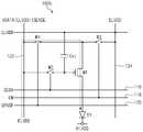
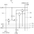
도 1을 참조하면, 화소 회로(102)는 유기 EL 소자(D1), 구동 트랜지스터(M1), 선택 트랜지스터(M2), 스위칭 트랜지스터(M3), 스위칭 트랜지스터(M4), 및 축적 용량(Cst)을 포함한다.1, the
구동 트랜지스터(M1)의 드레인 전극은 유기 EL 소자(D1)의 애노드측에 접속되다. 구동 트랜지스터(M1)의 게이트 전극의 전위는 데이터 신호선(122)에 접속된 선택 트랜지스터(M2)에 의해 제어된다. 축적 용량(Cst)은 구동 트랜지스터(M1)의 게이트 전극과 고 전압 전원(ELVDD)을 제공받는 전원선(124) 사이에 접속된다. 축적 용량(Cst)은 구동 트랜지스터(M1)의 게이트 전위를 충전할 수 있다.The drain electrode of the driving transistor M1 is connected to the anode side of the organic EL element D1. The potential of the gate electrode of the driving transistor Ml is controlled by the selection transistor M2 connected to the data signal
선택 트랜지스터(M2)의 게이트 전극은 선택 신호선(116)에 접속된다. 선택 트랜지스터(M2)는 선택 신호선(116)을 통해 제공받는 선택 신호에 응답하여, 데이터 신호선(122)로부터 제공받는 데이터 신호에 대응하는 전위를 구동 트랜지스터(M1)의 게이트 전극에 제공한다. 구동 트랜지스터(M1)의 소스 전극과 전원선(124) 사이에는 스위칭 트랜지스터(M3)가 접속된다.The gate electrode of the selection transistor M2 is connected to the
스위칭 트랜지스터(M3)의 게이트 전극은 유기 EL 소자(D1)의 발광 타이밍을 제어하기 위해 발광 제어선(118)에 접속된다. 또한, 구동 트랜지스터(M1)의 소스 전극과 데이터 신호선(122) 사이에 스위칭 트랜지스터(M4)가 접속된다. 스위칭 트랜지스터(M4)의 게이트 전극은 선택 신호선(120)에 접속된다.The gate electrode of the switching transistor M3 is connected to the
구동 트랜지스터(M1)의 게이트 전극에 소정의 전위가 제공되고, 스위칭 트랜지스터(M3)가 온 되면, 유기 EL 소자(D1)의 애노드측은 전원선(124)과 전기적으로 접속되고, 캐소드측은 저 전압 전원(ELVSS)을 제공받는 전원선(126)과 전기적으로 접속됨으로써, 유기 EL 소자(D1)가 발광된다.The anode side of the organic EL element D1 is electrically connected to the
도 2는 본 발명의 제1 실시 예에 따른 전기 광학 장치의 구동 방법을 나타내는 도면이다.2 is a view showing a driving method of the electro-optical device according to the first embodiment of the present invention.
도 2를 참조하면, 1 프레임 기간에서, 모든 화소들에 데이터 프로그래밍이 수행된 후, 모든 화소들이 동시에 발광된다. 발광 기간에서, 화소가 선택되어 구동 트랜지스터의 문턱 전압이 검출되거나 유기 EL 소자의 전압-전류 특성이 측정될 수 있다.Referring to FIG. 2, in one frame period, after data programming is performed on all the pixels, all pixels are simultaneously emitted. In the light emission period, a pixel is selected to detect the threshold voltage of the driving transistor or the voltage-current characteristic of the organic EL element can be measured.
예를 들어, 특정 화소의 구동 트랜지스터의 문턱 전압을 검출하기 위해, 1 프레임 기간 중 발광 기간에서, 데이터 신호선의 프리 차지가 수행되고, 검출 회로의 어드레스가 측정 대상의 특정 화소의 어드레스로 세트(또는 설정)되고, 특정 화소의 구동 트랜지스터로 전류가 인가되어 전압이 측정된다.For example, in order to detect the threshold voltage of the driving transistor of a specific pixel, precharging of the data signal line is performed in the light emitting period of one frame period, and the address of the detecting circuit is set to the address And a current is applied to the driving transistor of the specific pixel to measure the voltage.
또한, 특정 화소의 유기 EL 소자의 전압-전류 특성을 측정하기 위해, 1 프레임 기간 중 발광 기간에서, 데이터 신호선의 프리 차지가 수행되고, 검출 회로의 어드레스가 측정 대상의 특정 화소의 어드레스로 세트되고, 특정 화소의 유기 EL 소자로 전류가 인가되어 전압이 측정된다.In order to measure the voltage-current characteristics of the organic EL element of a specific pixel, precharging of the data signal line is performed in the light emission period of one frame period, and the address of the detection circuit is set to the address of the specific pixel to be measured , A current is applied to the organic EL element of a specific pixel and the voltage is measured.
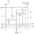
도 3은 본 발명의 제1 실시 예에 따른 전기 광학 장치의 패널 구성도이다.3 is a panel configuration diagram of an electro-optical device according to the first embodiment of the present invention.
도 3을 참조하면, 스캔 드라이버(104)는 제어 신호(Control signal)에 응답하여 선택 신호선(116)을 통해 선택 신호를 출력한다. 센스 드라이버(106)는 선택 신호선(120) 및 발광 제어선(118)을 통해 신호를 출력한다. 데이터 드라이버(108)은 데이터 신호선(122)을 통해 영상 신호에 대응하는 데이터 신호를 출력한다.Referring to FIG. 3, the
보정값 검출 회로(110)은 검출 신호선(130)에 접속된다. 보정값 검출 회로(110)는, 전환 회로(115)에 의해 검출 신호선(130)과 데이터 신호선(122)이 접속되면, 데이터 신호선(122)에 일정한 검출 전류를 제공한다.The correction
보정값 검출 회로(110)는 데이터 신호선(122)에 일정한 검출 전류를 제공했을때의 데이터 선의 전압 값(구동 트랜지스터의 소스 전극의 전압)을 측정하는 센스 회로(111), 센스 회로(111)의 출력 값을 A/D 변환하는 A/D 변환 회로(112), A/D 변환 후의 데이터를 저장하는 메모리(113), 및 메모리(113)로부터 제공받은 데이터를 이용하여 보정 값을 산출하는 연산 회로(114)를 포함한다. 연산 회로(114)의 출력 값은 보정 값으로서 데이터 드라이버(108)로 제공된다.The correction
데이터 드라이버(108)로부터 데이터 신호(VDATA)가 데이터 신호선(122)에 제공되고, 보정값 검출 회로(110)로부터 검출 전류(ISENSE)가 데이터 신호선(122)에 제공된다. 또한, 검출 대상의 화소와 같은 행에 속하는 화소 회로들(102)에 유기 EL 소자를 발광시키기 위한 전원 전압(ELVDD)이 제공되어야 하며, 이러한 전원 전압(ELVDD)이 데이터 신호선(122)에 제공된다.A data signal VDATA is supplied from the
이와 같이 데이터 신호선(122)에 소정의 타이밍에 따라서 다른 전압(혹은 전류)의 신호가 제공되어야 한다. 이를 위해, 전환 회로(115)는 소정의 타이밍에 따라서 다른 전압의 신호를 선택적으로 출력할 수 있다.In this manner, a signal of a different voltage (or current) must be provided to the data signal
도 4는 본 발명의 제1 실시 예에 따른 전기 광학 장치의 패널의 센싱 시의 패널 상태도이다.4 is a panel state view of a panel of an electro-optical device according to the first embodiment of the present invention at the time of sensing.
도 4를 통해 검출 대상의 특정 화소에 대한 센싱 동작이 설명될 것이다.The sensing operation for a specific pixel of a detection object will be described with reference to FIG.
도 4를 참조하면, 검출 대상 화소는, 화소 (102a)로 나타낸다. 그리고 화소(102a)와 동일한 발광 제어선(118)에 연결된 화소들은 화소(102b)로 나타내고, 그 이외의 화소들은 화소(102c)로 나타낸다.Referring to Fig. 4, the pixel to be detected is represented by a
화소(102c)는 통상적으로 동작하는 화소로서, 발광 기간에서, 유기 EL 소자(D1)가 구동 트랜지스터(M1) 및 스위칭 트랜지스터(M3)를 통해 전원선(124)에 접속되어 있으므로, 구동 트랜지스터(M1)의 드레인 전류에 기초하여 화소(102c)의 유기 EL 소자(D1)가 발광된다.Since the
화소(102b)는, 스위칭 트랜지스터(M3)가 오프 되어 있어, 전원선(124)과 오픈되어 있다. 그러나, 화소(102b)는, 스위칭 트랜지스터(M4)가 온 이기 때문에, 데이터 신호선(122)으로부터 전원 전압(ELVDD)을 제공받으므로, 구동 트랜지스터(M1)의 드레인 전류에 기초하여 화소(102b)의 유기 EL 소자(D1)가 발광된다.In the
전환 회로(115)는 검출 신호선(130)과 전원선(124)의 접속을 선택하는 스위칭 트랜지스터를 포함한다. 전환 회로(115)는 검출 대상 화소(102a)가 배치된 열의 데이터 신호선(122) 이외의 데이터 신호선들(122)이 전원선(124)와 접속되도록 동작한다.The
검출 대상 화소(102a)의 데이터 신호선(122)은 전환 회로(115)의 스위칭 트랜지스터에 의해 보정값 검출 회로(110)에 접속된다. 화소(102a)에서 스위칭 트랜지스터(M4)가 온 됨으로써, 보정값 검출 회로(110)와 접속된 검출 신호선(130)을 통해 검출 전류가 구동 트랜지스터(M4)로 제공되고, 그 때의 구동 트랜지스터(M4)의 소스 전극의 전압이 센스 회로(111)에 의해 검출된다.The data signal
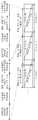
도 5a 내지 도 5f는 본 발명의 제1 실시 예에 따른 전기 광학 장치의 화소의 기본 동작을 나타내는 도면이다.5A to 5F are diagrams showing basic operations of pixels of the electro-optical device according to the first embodiment of the present invention.
도 5a 내지 도 5f에는 본 발명의 제1 실시 예에 따른 전기 광학 장치의 검출 동작시 화소(102a), 화소(102b), 및 화소(102c)의 구체적인 동작이 도시되었다.5A to 5F show specific operations of the
도 5a 및 도 5b는 화소(102a)의 동작을 설명하기 위한 도면이다. 도 5c 및 도 5d는 화소(102b)의 동작을 설명하기 위한 도면이다. 도 5e 및 도 5f는 화소(102c)의 동작을 설명하기 위한 도면이다.5A and 5B are diagrams for explaining the operation of the
도 5a를 참조하면, 검출 대상 화소(102a)에, 데이터가 기입될 때, 선택 트랜지스터(M2)가 온 되어, 구동 트랜지스터(M1)의 게이트 전극에 검출용 데이터가 기입된다.Referring to FIG. 5A, when data is written in the
도 5b를 참조하면, 선택 트랜지스터(M2)가 오프된 후, 데이터 신호선(122)에 검출 전류(ISENSE)가 제공되고, 스위칭 트랜지스터(M4)가 온 된다. 이 때의 데이터 신호선의 전압값(구동 트랜지스터의 소스 전극의 전압)을 보정값 검출 회로(110)가 측정함으로써, 구동 트랜지스터(M1)의 문턱 전압 또는 유기 EL 소자(D1)의 전압-전류 특성이 측정될 수 있다.Referring to FIG. 5B, after the selection transistor M2 is turned off, a detection current ISENSE is provided to the data signal
도 5c를 참조하면, 검출 대상 화소(102a)와 같은 선택 신호선(120)에 연결된 다른 화소(102b)에 데이터가 기입될때, 선택 트랜지스터(M2)가 온 되어, 구동 트랜지스터(M1)의 게이트 전극에 데이터 전압(VDATA)이 기입된다.5C, when data is written to the
도 5d를 참조하면, 선택 신호선(120)에 의해 스위칭 트랜지스터(M4)가 온 되어, 전원 전압(ELVDD)이 제공된 데이터 신호선(122)과 구동 트랜지스터(M1)가 접속된다. 따라서, 구동 트랜지스터(M1)의 드레인 전류에 기초하여 유기 EL 소자(D1)가 발광된다.5D, the switching transistor M4 is turned on by the
도 5e를 참조하면, 그 이외의 화소(102c)에 데이터가 기입될 때, 선택 트랜지스터(M2)가 온 되어, 구동 트랜지스터(M1)의 게이트 전극에 데이터 전압(VDATA)이 기입된다.Referring to FIG. 5E, when data is written to the
도 5f를 참조하면, 스위칭 트랜지스터(M3)가 온 되어 전원선(124)과 구동 트랜지스터(M1)가 접속된다. 따라서, 구동 트랜지스터(M1)의 드레인 전류에 기초하여 유기 EL 소자(D1)가 발광된다.Referring to FIG. 5F, the switching transistor M3 is turned on, and the
도 6a 및 도 6b는 센싱 시의 구동 트랜지스터의 소스 전압 변화를 나타내는 도면이다.6A and 6B are diagrams showing changes in the source voltage of the driving transistor at the time of sensing.
도 6a를 참조하면, 구동 트랜지스터의 문턱 전압을 검출하기 위해, 구동 트랜지스터가 포화 영역에서 동작되도록 구동 트랜지스터의 게이트 전극에 검출용 전압이 제공될 수 있다.Referring to FIG. 6A, in order to detect the threshold voltage of the driving transistor, a detection voltage may be provided to the gate electrode of the driving transistor so that the driving transistor is operated in the saturation region.
도 6a에 도시된 바와 같이, 구동 트랜지스터가 포화 영역에서 동작될 때, 어떤 일정한 소스 전류가 제공되면, 구동 트랜지스터의 소스 전압은 구동 트랜지스터의 문턱 전압에 의해 변화된다. 따라서, 구동 트랜지스터의 전압값을 검출함으로써, 문턱 전압이 측정될 수 있다.As shown in Fig. 6A, when the driving transistor is operated in the saturation region, if a constant source current is provided, the source voltage of the driving transistor is changed by the threshold voltage of the driving transistor. Therefore, by detecting the voltage value of the driving transistor, the threshold voltage can be measured.
도 6b를 참조하면, 유기 EL 소자의 전압-전류 특성을 구하기 위해, 구동 트랜지스터가 선형 영역에서 동작되도록 구동 트랜지스터의 게이트 전극에 검출용 전압이 제공될 수 있다.Referring to FIG. 6B, a voltage for detection may be provided to the gate electrode of the driving transistor so that the driving transistor is operated in a linear region, in order to obtain the voltage-current characteristic of the organic EL element.
도 6b에 나타내는 바와 같이, 구동 트랜지스터가 선형 영역에서 동작될 때, 어떤 일정한 소스 전류가 제공되면, 구동 트랜지스터의 소스 전압은 유기 EL 소자의 동작 전압에 의해 변화된다. 따라서, 유기 EL 소자의 전압값을 검출함으로써, 유기 EL 소자의 열화의 정도가 측정될 수 있다.As shown in Fig. 6B, when a constant source current is provided when the driving transistor is operated in the linear region, the source voltage of the driving transistor is changed by the operating voltage of the organic EL element. Therefore, by detecting the voltage value of the organic EL element, the degree of deterioration of the organic EL element can be measured.
이러한 회로 구성과 그 동작에 의해, 검출 대상 화소는 데이터 신호에 대응하는 발광 동작을 하지 않는다. 그러나, 그 이외의 화소는 검출 대상 화소와 같은 행에 배치된 화소라도, 통상적인 발광 동작을 수행할 수 있다.With such a circuit configuration and its operation, the detection subject pixel does not emit light corresponding to the data signal. However, even if the pixels other than the pixels are arranged in the same row as the detection subject pixel, a normal light emission operation can be performed.
즉, 본 발명의 실시 예에 따른 전기 광학 장치는 특정 화소만을 검출 대상으로 지정하여 구동 트랜지스터의 문턱 전압 또는 유기 EL 소자의 전압-전류 특성을 측정하고, 검출 대상 화소 이외의 다른 화소들을 통상적으로 발광 시킬 수 있다. 이러한 동작에 의해, 영상이 표시될 때, 선 결함이 발생되지 않고, , 특정 화소의 보상 데이터가 취득될 수 있다.That is, in the electro-optical device according to the embodiment of the present invention, only a specific pixel is designated as a detection target, the threshold voltage of the driving transistor or the voltage-current characteristic of the organic EL element is measured, . With this operation, when an image is displayed, no line defect is generated, and compensation data of a specific pixel can be obtained.
또한, 보정값 검출 회로가 복수 개 사용될 경우, 매트릭스 형상으로 배열된 복수의 화소들 중, 다른 행에 속하는 복수의 화소들에 대해서 검출 동작이 동시에 수행될 수도 있다.When a plurality of correction value detection circuits are used, the detection operation may be performed simultaneously on a plurality of pixels belonging to different rows among a plurality of pixels arranged in a matrix.
검출 동작이 수행될 때, 검출 동작이 수행되는 임의의 한 행에 배치된 화소가 통상적인 발광 동작을 하지 않을 경우, 선 결함으로서 사용자에게 시인될 수 있다.When a detection operation is performed, a pixel arranged in any one row in which a detection operation is performed can be visually recognized as a line defect, if the pixel does not perform a normal light emitting operation.
그러나, 본 발명의 실시 예에 따른 전기 광학 장치가 복수의 화소들을 이용하여 영상을 표시하더라도, 몇 개의 화소가 이산적으로 검출 동작을 수행하므로, 검출 동작이 수행되는 화소가 사용자의 눈에 띠이지 않을 수 있다.However, even when the electro-optical device according to the embodiment of the present invention displays an image using a plurality of pixels, since a few pixels discretionally perform the detection operation, the pixel on which the detection operation is performed is striped .
이와 같이, 본 발명의 실시 예에 따른 전기 광학 장치는 검출 대상 화소를 개별적으로 선택하여 보정 데이터를 취득하면서, 다른 화소들을 통상적으로 발광시켜 영상을 표시 할 수 있다. 따라서, 종래 기술의 문제점인 선 결함이 발생되지 않아, 표시 품질을 저하시키지 않고 보정 동작이 수행될 수 있다.As described above, the electro-optical device according to the embodiment of the present invention can display an image by normally emitting other pixels while acquiring correction data by individually selecting detection target pixels. Therefore, a line defect, which is a problem of the prior art, is not generated, and the correction operation can be performed without lowering the display quality.
[실시 형태 2] [Embodiment 2]
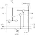
도 7은 본 발명의 제2 실시 예에 따른 전기 광학 장치의 화소 구성도이다.7 is a diagram showing the pixel configuration of the electro-optical device according to the second embodiment of the present invention.
도 7을 참조하면, 본 발명의 제2 실시 예에 따른 전기 광학 장치의 화소 회로(102)는 도 1에 도시된 화소 회로와 같이, 유기 EL 소자(D1), 4개의 트랜지스터들(M1~M4), 및 1 개의 용량 소자(Cst)를 포함한다.7, the
도 7에 도시된 화소 회로(102)는 도 1에 도시된 화소 회로(102)와 달리 검출 대상 화소에 제공되는 검출용 전류(ISENSE)와, 전원 전압(ELVDD)을 데이터 신호선(122)에 제공하지 않고, 추가적인 센스 신호선(128)에 제공한다.The
구동 트랜지스터(M1)의 드레인 전극은 유기 EL 소자(D1)의 애노드측과 접속되고, 소스 전극은 스위칭 트랜지스터(M3)을 통해 전원선(124)에 접속된다. 또한, 구동 트랜지스터(M1)의 소스 전극은 스위칭 트랜지스터(M4)과 접속된.The drain electrode of the driving transistor M1 is connected to the anode side of the organic EL element D1 and the source electrode thereof is connected to the
스위칭 트랜지스터(M4)는 검출용 전류(ISENSE)와 전원 전압(ELVDD)이 제공되는 센스 신호선(128)과 구동 트랜지스터(M1)의 소스 전극의 접속을 선택하는 선택 신호선(120)에 접속된다. 유기 EL 소자(D1)가 발광하는 타이밍은 게이트 전극이 발광 제어선(118)에 접속되는 스위칭 트랜지스터(M3)에 의해 제어된다.The switching transistor M4 is connected to the
도 8은 본 발명의 제2 실시 예에 따른 전기 광학 장치의 구동 방법을 나타내는 도면이다.8 is a diagram showing a driving method of an electro-optical device according to a second embodiment of the present invention.
도 8을 참조하면, 1 프레임 기간에서, 화소들에 데이터 프로그래밍과 발광이 점차적으로 수행된다. 이러한 구동 방법을 프로그레시브 구동이라 한다.Referring to FIG. 8, in one frame period, data programming and light emission are gradually performed on the pixels. This driving method is referred to as progressive driving.
이 경우, 특정 화소의 구동 트랜지스터 문턱 전압을 검출하기 위해, 어떤 1 프레임 기간에서, 검출 회로의 어드레스가 측정 대상의 특정 화소의 어드레스로 세트되고, 특정 화소의 구동 트랜지스터로 전류가 인가되어 전압이 측정된다.In this case, in order to detect the threshold voltage of the driving transistor of a specific pixel, the address of the detection circuit is set to an address of a specific pixel to be measured in one frame period, and a current is applied to the driving transistor of the specific pixel do.
이러한 동작은 다음의 1 프레임 기간에서 상기 화소에 데이터가 기입되는 기간이 될 때까지 수행될 수 있다. 또한, 다음의 1 프레임 기간의 발광 기간에서서, 유기 EL 소자의 전압-전류 특성을 측정하기 위해, 검출 회로의 어드레스가 측정 대상의 특정 화소의 어드레스로 세트되고, 특정 화소의 유기 EL 소자로 전류가 인가되어 및 전압이 측정된다.This operation can be performed until a period in which data is written to the pixel in the next one frame period. Further, in order to measure the voltage-current characteristic of the organic EL element in the light emission period of the next one frame period, the address of the detection circuit is set to the address of the specific pixel to be measured, And the voltage is measured.
구동 트랜지스터의 문턱 전압의 검출 및 유기 EL 소자의 전압-전류 특성의 측정은 연속하는 프레임 기간에 수행될 수 도 있고, , 어떤 프레임 기간과, 그것과 시간적으로 떨어진 별개의 프레임 기간에 수행될 수도 있다.The detection of the threshold voltage of the driving transistor and the measurement of the voltage-current characteristic of the organic EL element may be performed in successive frame periods and may be performed in a certain frame period and in separate frame periods temporally separated from it .
도 9는 본 발명의 제2 실시 예에 따른 전기 광학 장치의 패널 구성도이다.9 is a panel configuration diagram of an electro-optical device according to the second embodiment of the present invention.
도 9를 참조하면, 스캔 드라이버(104), 센스 드라이버(106), 데이터 드라이버(108), 및 보정값 검출 회로(110)의 구성은 도 3에 도시된 스캔 드라이버(104), 센스 드라이버(106), 데이터 드라이버(108), 및 보정값 검출 회로(110)와 동일하다. 단, 도 3과 달리 도 9에는, 센스 신호선(128)이 추가되어 있다. 센스 신호선(128)으로 인해 전환 회로(115)의 트랜지스터의 연결 구성이 도 3과 다르다. 구체적으로, 전환 회로(115)의 센스 신호선(128)이 보정값 검출 회로(110) 또는 전원선(124)에 접속되도록 스위칭 트랜지스터가 배치된다.9, the configurations of the
도 10은 본 발명의 제2 실시 예에 따른 패널의 센싱 시의 패널 상태도이다.FIG. 10 is a panel state diagram at the time of sensing the panel according to the second embodiment of the present invention. FIG.
도 10을 통해 검출 대상의 특정 화소에 대한 센싱 동작이 설명될 것이다.The sensing operation for a specific pixel of a detection object will be described with reference to FIG.
도 10을 참조하면, 검출 대상 화소는, 화소(102a)로 나타낸다. 화소(102a)와 동일한 발광 제어선(118)에 연결된 화소들은 화소(102b)로 나타내고, 그 이외의 화소들은 화소(102c)로 나타낸다.Referring to Fig. 10, the pixel to be detected is represented by a
화소(102c)는 통상적인 동작을 하는 화소이다. 발광 기간에서, 화소(102c)의 유기 EL 소자(D1)는 구동 트랜지스터(M1) 및 스위칭 트랜지스터(M3)를 통해 전원선(124)과 접속되어서, 구동 트랜지스터(M1)의 드레인 전류에 기초하여 발광된다.The
화소(102b)의 유기 EL 소자(D1)는 스위칭 트랜지스터(M3)가 오프 되므로되어 전원선(124)과 오픈 된다. 그러나 화소(102b)의 유기 EL 소자(D1)는 스위칭 트랜지스터(M4)가 온 되므로 전원 전압(ELVDD)이 제공된 센스 신호선(128)과 접속된다. 따라서, 구동 트랜지스터(M1)의 드레인 전류가 화소(102b)의 유기 EL 소자(D1)에 제공되어 화소(102b)의 유기 EL 소자(D1)가 발광된다.The organic EL element D1 of the
검출 대상 화소(102a)의 센스 신호선(128)은 전환 회로(115)의 스위칭 트랜지스터에 의해 검출 신호선(130)에 접속된다. 검출 신호선(130)은 보정값 검출 회로(110)에 접속되어 있다. 화소(102a)에서 스위칭 트랜지스터(M4)가 온 되므로, 센스 신호선(128)에 제공된 검출 전류가 구동 트랜지스터(M4)에 제공되고, 그 때의 구동 트랜지스터(M4)의 소스 전극의 전압이 보정값 검출 회로에 의해 검출된다.The
도 11a 내지 도 11f는 본 발명의 제2 실시 예에 따른 화소의 기본 동작을 나타내는 도면이다.11A to 11F are diagrams showing basic operations of a pixel according to a second embodiment of the present invention.
도 11a 내지 도 11f에는 본 발명의 제2 실시 예에 따른 전기 광학 장치의 검출 동작시 화소(102a), 화소(102b), 및 화소(102c)의 구체적인 동작이 도시되었다.11A to 11F show specific operations of the
도 11a 및 도 11b는 화소(102a)의 동작을 설명하기 위한 도면이다. 도 11c 및 도 11d는 화소(102b)의 동작을 설명하기 위한 도면이다. 도 11e 및 도 11f는 화소(102c)의 동작을 설명하기 위한 도면이다.11A and 11B are diagrams for explaining the operation of the
도 11a를 참조하면, 검출 대상 화소에, 데이터가 기입될 때, 선택 트랜지스터(M2)가 온 되어, 구동 트랜지스터(M1)의 게이트 전극에 검출용 데이터가 기입된다.Referring to Fig. 11A, when data is written to the detection subject pixel, the selection transistor M2 is turned on, and the detection data is written to the gate electrode of the driving transistor M1.
도 11b를 참조하면, 선택 트랜지스터(M2)가 오프된 후, 센스 신호선(128)에 검출 전류(ISENSE)가 제공되고, 스위칭 트랜지스터(M4)가 온 된다. 이 때의 데이터 신호선의 전압값(구동 트랜지스터의 소스 전극의 전압)을 보정값 검출 회로(110)가 측정함으로써, 구동 트랜지스터(M1)의 문턱 전압 또는 유기 EL 소자(D1)의 전압-전류 특성이 측정될 수 있다.Referring to FIG. 11B, after the selection transistor M2 is turned off, a sense current ISENSE is provided to the
도 11c를 참조하면, 검출 대상 화소(102a)와 같은 선택 신호선(120)에 연결된 다른 화소(102b)에 데이터가 기입될 때, 선택 트랜지스터(M2)가 온 되어 구동 트랜지스터(M1)의 게이트 전극에 데이터 전압(VDATA)이 기입된다.11C, when data is written to the
도 11d를 참조하면, 선택 신호선(120)에 의해 스위칭 트랜지스터(M4)가 온 되어, 전원 전압(ELVDD)이 제공된 센스 신호선(128)과 구동 트랜지스터(M1)가 접속된다. 따라서, 구동 트랜지스터(M1)의 드레인 전류에 기초하여 유기 EL 소자(D1)가 발광된다.11D, the switching transistor M4 is turned on by the
도 11e를 참조하면, 그 이외의 화소(102c)에 데이터가 기입될 때, 선택 트랜지스터(M2)가 온 되어 구동 트랜지스터(M1)의 게이트 전극에 데이터 전압(VDATA)이 기입된다.Referring to FIG. 11E, when data is written to the
도 11f를 참조하면, 스위칭 트랜지스터(M3)가 온 되어 전원선(124)과 구동 트랜지스터(M1)가 접속된다. 따라서, 구동 트랜지스터(M1)의 드레인 전류에 기초하여 유기 EL 소자(D1)가 발광된다.Referring to FIG. 11F, the switching transistor M3 is turned on, and the
본 발명의 제2 실시 예에서, 데이터 신호선과 센스 신호선을 분리함으로써, 데이터 프로그램 시에도 측정 동작이 수행될 수 있고, 1 프레임 기간 중의 어떤 기간이라도 측정 동작이 수행될 수 있다. 즉, 본 발명의 제1 실시 예에서는 발광 기간에 서만 측정 동작이 수행될 수 있지만, 본 발명의 제2 실시 예에서는 모든 기간에서 측정 동작이 수행될 수 있기 때문에, 모든 화소를 측정하는 시간이 단축될 수 있다. 또한, 표시 품질이 저하되지 않고, 보정 동작이 수행될 수 있는 이점은 실시 예 1과 같다.In the second embodiment of the present invention, by separating the data signal line and the sense signal line, the measurement operation can be performed even in the data programming, and the measurement operation can be performed in any period of one frame period. That is, in the first embodiment of the present invention, the measurement operation can be performed only in the light emission period. However, since the measurement operation can be performed in all the periods in the second embodiment of the present invention, . Further, the advantage that the display quality is not deteriorated and the correcting operation can be performed is the same as the first embodiment.
이상 실시 예를 참조하여 설명하였지만, 해당 기술 분야의 숙련된 당업자는 하기의 특허 청구의 범위에 기재된 본 발명의 사상 및 영역으로부터 벗어나지 않는 범위 내에서 본 발명을 다양하게 수정 및 변경시킬 수 있음을 이해할 수 있을 것이다. 또한 본 발명에 개시된 실시 예는 본 발명의 기술 사상을 한정하기 위한 것이 아니고, 하기의 특허 청구의 범위 및 그와 동등한 범위 내에 있는 모든 기술 사상은 본 발명의 권리범위에 포함되는 것으로 해석되어야 할 것이다.It will be understood by those skilled in the art that various changes in form and details may be made therein without departing from the spirit and scope of the invention as defined in the appended claims. It will be possible. In addition, the embodiments disclosed in the present invention are not intended to limit the technical spirit of the present invention, and all technical ideas which fall within the scope of the following claims and equivalents thereof should be interpreted as being included in the scope of the present invention .
102 : 화소 회로104 : 스캔 드라이버
106 : 센스 드라이버108 : 데이터 드라이버
110 : 보정값 검출 회로111 : 센스 회로
112 : A/D 변환 회로113 : 메모리
114 : 연산 회로115 : 전환 회로
116 : 선택 신호선118 : 발광 제어선
120 : 선택 신호선122 : 데이터 신호선
124 : 전원선126 : 전원선
128 : 센스 신호선130 : 검출 신호선
M1 : 구동 트랜지스터M2 : 선택 트랜지스터
M3 : 스위칭 트랜지스터M4 : 스위칭 트랜지스터
D1 : 유기 EL 소자Cst : 축적 용량102: pixel circuit 104: scan driver
106: sense driver 108: data driver
110: correction value detection circuit 111: sense circuit
112: A / D conversion circuit 113: memory
114: Operation circuit 115:
116: selection signal line 118: emission control line
120: selection signal line 122: data signal line
124: power line 126: power line
128: sense signal line 130: detection signal line
M1: driving transistor M2: selection transistor
M3: switching transistor M4: switching transistor
D1: organic EL element Cst: storage capacity
Claims (10)
Translated fromKorean데이터 프로그래밍 기간에서, 상기 선택 트랜지스터가 온 되고, 상기 구동 트랜지스터의 상기 게이트 전극에 상기 데이터 신호선으로부터 데이터 전압이 제공되고,
발광 기간에서,
상기 행 방향 및 상기 열 방향으로 배열된 상기 화소들 중 검출 대상 화소에서, 상기 제 1 스위칭 트랜지스터가 오프 되고, 상기 제 2 스위칭 트랜지스터가 온 됨으로써, 상기 구동 트랜지스터의 상기 소스 전극이 상기 데이터 신호선에 접속되어, 상기 데이터 신호선으로부터 검출용 전류가 상기 상기 구동 트랜지스터에 제공되고,
상기 행 방향 및 상기 열 방향으로 배열된 상기 화소들 중, 상기 검출 대상 화소와 같은 행에 배열된 화소들 각각에서, 상기 제 1 스위칭 트랜지스터가 오프 되고, 상기 제 2 스위칭 트랜지스터가 온 됨으로써, 상기 구동 트랜지스터의 상기 소스 전극이 상기 데이터 신호선에 접속되어, 상기 데이터 신호선로부터 상기 전원선과 같은 전원 전압이 상기 구동 트랜지스터에 제공되고,
상기 화소들 중, 상기 검출 대상 화소와 다른 행에 배열된 화소들 각각에서, 상기 제 1 스위칭 트랜지스터가 온 되고, 상기 제 2 스위칭 트랜지스터가 오프 됨으로써, 상기 구동 트랜지스터의 상기 소스 전극이 상기 전원선과 접속되어 상기 유기 일렉트로루미네센스 소자가 발광하는 것을 특징으로 하는 화소 회로.A driving transistor to which the anode side and the drain electrode of the organic electroluminescence element are connected; A selection transistor for controlling a connection between a gate electrode of the driving transistor and a data signal line; A first switching transistor for controlling connection between a source electrode of the driving transistor and a power supply line for supplying current to the organic electroluminescence element; And a plurality of pixels each having a second switching transistor for controlling a connection between the source electrode of the driving transistor and the data signal line, the pixels being arranged in a row direction and a column direction,
In the data programming period, the selection transistor is turned on, the gate electrode of the driving transistor is supplied with the data voltage from the data signal line,
In the light emission period,
The first switching transistor is turned off and the second switching transistor is turned on at the detection target pixel among the pixels arranged in the row direction and the column direction so that the source electrode of the driving transistor is connected to the data signal line A detection current is supplied to the driving transistor from the data signal line,
The first switching transistor is turned off and the second switching transistor is turned on in each of the pixels arranged in the same row as the detection subject pixel among the pixels arranged in the row direction and the column direction, The source electrode of the transistor is connected to the data signal line, a power supply voltage, such as the power supply line, is provided to the driving transistor from the data signal line,
The first switching transistor is turned on and the second switching transistor is turned off in each of the pixels arranged in rows different from the detection subject pixel among the pixels so that the source electrode of the driving transistor is connected to the power line And the organic electroluminescence element emits light.
상기 유기 일렉트로루미네센스 소자가 동시에 발광하는 발광 기간에서, 상기 화소들 중, 검출 대상 화소에서, 상기 데이터 신호선으로부터 상기 구동 트랜지스터의 소스 전극에 검출용 전류를 제공하고, 상기 구동 트랜지스터가 포화 영역에서 동작할 때 또는 상기 구동 트랜지스터가 선형 영역에서 동작할 때의 상기 구동 트랜지스터의 상기 소스 전극의 전압을 검출하고, 상기 화소들 중 상기 검출 대상 화소 이외의 화소들에서, 상기 구동 트랜지스터의 상기 게이트 전극의 전위를 충전한 상태에서, 상기 구동 트랜지스터의 상기 소스 전극을 전원선과 접속시켜 상기 유기 일렉트로루미네센스 소자를 동시에 발광시키는 것을 특징으로 하는 화소 회로의 구동 방법.Data programming for providing the gate potential from the data signal line to the gate electrode of the driving transistor to which the anode side and the drain electrode of the organic electroluminescence element provided in each of the plurality of pixels arranged in the row direction and the column direction are connected, , ≪ / RTI >
In the light emission period in which the organic electroluminescence element emits light simultaneously, a detection current is supplied to the source electrode of the driving transistor from the data signal line in the detection target pixel among the pixels, Wherein the voltage of the source electrode of the driving transistor is detected when the driving transistor operates in a linear region or in a region other than the pixel to be detected among the pixels, Wherein the source electrode of the driving transistor is connected to a power supply line while the organic electroluminescence element is lighted at the same time with the electric potential charged.
상기 데이터 프로그래밍이 종료된 화소부터 상기 구동 트랜지스터의 게이트 전극의 전위를 충전한 상태에서, 상기 구동 트랜지스터의 소스 전극을 전원선과 접속시켜 상기 유기 일렉트로루미네센스 소자를 발광시키고,
상기 1 프레임 기간에서, 상기 화소들 중 검출 대상 화소에서는, 상기 데이터 신호선으로부터 상기 구동 트랜지스터의 소스 전극에 소스 전류를 제공하고, 상기 구동 트랜지스터가 포화 영역에서 동작할 때 또는 상기 구동 트랜지스터가 선형 영역에서 동작할 때의 상기 구동 트랜지스터의 상기 소스 전극의 전압을 검출하는 것을 특징으로 하는 화소 회로의 구동 방법.The data programming for providing the gate potential from the data signal line to the gate electrode of the driving transistor to which the anode side and the drain electrode of the organic electroluminescence element provided in each of the plurality of pixels arranged in the row direction and the column direction are connected, And then,
A source electrode of the driving transistor is connected to a power supply line to emit the organic electroluminescence element in a state in which the potential of the gate electrode of the driving transistor is filled from the pixel where the data programming is completed,
A source current is supplied to the source electrode of the driving transistor from the data signal line in the detection target pixel among the pixels, and when the driving transistor operates in the saturation region or when the driving transistor is in the linear region And the voltage of the source electrode of the driving transistor when the pixel is driven.
상기 데이터 신호선의 접속 위치를 전환하는 전환 회로를 더 포함하고,
상기 전환 회로는, 상기 각 화소의 상기 구동 트랜지스터의 게이트 전극에 데이터 전압을 기입하는 데이터 프로그래밍 기간에서 상기 데이터 신호선을 상기 데이터 드라이버에 접속시키고, 상기 각 화소가 발광하는 발광 기간에서 상기 데이터 신호선을 상기 전원선에 접속시키고, 상기 검출 대상 화소의 상기 구동 트랜지스터의 상기 소스 전극에 소스 전류를 공급할 때 상기 데이터 신호선을 상기 보정값 검출 회로에 접속시키는 것을 특징으로 하는 전기 광학 장치.5. The method of claim 4,
Further comprising a switching circuit for switching a connection position of the data signal line,
Wherein the switching circuit connects the data signal line to the data driver in a data programming period for writing a data voltage to the gate electrode of the driving transistor of each pixel, And the data signal line is connected to the correction value detecting circuit when the source current is supplied to the source electrode of the driving transistor of the detection target pixel.
상기 화소 회로는,
같은 열 방향으로 배열된 화소의 구동 트랜지스터의 소스 전극과 접속되는 검출 신호선; 및
상기 검출 신호선의 접속 위치를 변경하는 전환 회로를 더 포함하고,
상기 전환 회로는, 상기 검출 대상 화소의 상기 구동 트랜지스터의 소스 전극에 소스 전류를 공급할 때 상기 검출 신호선을 상기 보정값 검출 회로에 접속시키고, 상기 각 화소가 발광하는 발광 기간에서 상기 검출 신호선을 상기 전원선에 접속시키는 것을 특징으로 하는 전기 광학 장치.5. The method of claim 4,
The pixel circuit includes:
A detection signal line connected to the source electrode of the driving transistor of the pixel arranged in the same column direction; And
Further comprising a switching circuit for changing a connection position of the detection signal line,
Wherein the switching circuit connects the detection signal line to the correction value detection circuit when the source current is supplied to the source electrode of the driving transistor of the detection subject pixel and outputs the detection signal line to the power source Optical device according to claim 1,
상기 구동 트랜지스터의 상기 게이트 전극의 전위를 충전한 상태에서, 상기 구동 트랜지스터의 소스 전극을 전원선과 접속시키고, 상기 유기 일렉트로루미네센스 소자를 동시에 발광시키는 구동 방법에 있어서,
상기 유기 일렉트로루미네센스 소자가 동시에 발광하는 기간에서, 상기 화소들 중 보정값의 검출 대상으로 되는 화소의 어드레스를 설정하고, 상기 검출 대상 화소에서, 상기 구동 트랜지스터의 상기 소스 전극에 전류를 공급하고, 상기 구동 트랜지스터를 포화 영역에서 동작시켰을 때에 얻어지는 상기 구동 트랜지스터의 상기 소스 전극의 전압으로부터 상기 구동 트랜지스터의 문턱 전압을 검출하거나 또는 상기 구동 트랜지스터를 선형 영역에서 동작시켰을 때에 얻어지는 상기 구동 트랜지스터의 상기 소스 전극의 전압으로부터 상기 유기 일렉트로루미네센스 소자의 전압-전류 특성을 검출하고,
상기 검출된 데이터 값으로부터, 상기 구동 트랜지스터의 문턱 전압의 보정 데이터 또는 상기 유기 일렉트로루미네센스 소자의 보정 데이터를 생성하는 것을 특징으로 하는 전기 광학 장치의 구동 방법.A data programming for providing a gate potential from a data signal line to a driving transistor gate electrode to which an anode side and a drain electrode of an organic electroluminescence element provided in each of a plurality of pixels arranged in a row direction and a column direction are connected, , ≪ / RTI >
A driving method for connecting a source electrode of the driving transistor with a power supply line in a state in which the potential of the gate electrode of the driving transistor is charged and simultaneously causing the organic electroluminescence element to emit light,
An address of a pixel to be a detection target of a correction value among the pixels is set in a period during which the organic electroluminescence element emits light at the same time and a current is supplied to the source electrode of the driving transistor The source electrode of the driving transistor, which is obtained when the threshold voltage of the driving transistor is detected from the voltage of the source electrode of the driving transistor obtained when the driving transistor is operated in the saturation region, or when the driving transistor is operated in the linear region, Current characteristic of the organic electroluminescence element from the voltage of the organic electroluminescence element,
And generates correction data of the threshold voltage of the driving transistor or correction data of the organic electroluminescence element from the detected data value.
상기 유기 일렉트로루미네센스 소자가 모든 화소들에서 동시에 발광하는 기간에서, 상기 검출 대상 화소 및 상기 검출 대상 화소가 배치된 행의 화소들 이외의 화소들 각각에서, 상기 구동 트랜지스터의 상기 소스 전극을 상기 전원선과 접속시키고,
상기 검출 대상 화소가 배치된 행의 화소들 각각에서, 상기 구동 트랜지스터의 상기 소스 전극을 상기 데이터 신호선과 접속시키는 동시에, 상기 데이터 신호선을 상기 전원선과 접속시키는 것을 특징으로 하는 전기 광학 장치의 구동 방법.8. The method of claim 7,
In the period during which the organic electroluminescence element emits light simultaneously in all the pixels, in each of the pixels other than the pixels of the row in which the detection subject pixel and the detection subject pixel are arranged, the source electrode of the driving transistor Connected to a power line,
The source electrode of the driving transistor is connected to the data signal line and the data signal line is connected to the power source line in each of the pixels of the row in which the detection subject pixel is arranged.
상기 데이터 프로그래밍이 종료된 화소부터, 상기 구동 트랜지스터의 게이트 전극의 전위를 충전한 상태로, 상기 구동 트랜지스터의 소스 전극을 전원선과 접속시켜, 상기 유기 일렉트로루미네센스 소자를 발광시키는 구동 방법에 있어서,
상기 1 프레임 기간에서, 상기 화소들 중 보정값의 검출 대상으로 되는 화소의 어드레스를 설정하고, 상기 검출 대상 화소에서, 상기 구동 트랜지스터의 상기 소스 전극에 전류를 공급하고, 상기 구동 트랜지스터를 포화 영역에서 동작시켰을 때에 얻어지는 상기 구동 트랜지스터의 상기 소스 전극의 전압으로부터 상기 구동 트랜지스터의 문턱 전압을 검출하거나 또는 상기 구동 트랜지스터를 선형 영역에서 동작시켰을 때에 얻어지는 상기 구동 트랜지스터의 상기 소스 전극의 전압으로부터 상기 유기 일렉트로루미네센스 소자의 전압-전류 특성을 검출하고,
상기 검출된 데이터 값으로부터, 상기 구동 트랜지스터의 문턱 전압의 보정 데이터 또는 상기 유기 일렉트로루미네센스 소자의 보정 데이터를 생성하는 것을 특징으로 하는 전기 광학 장치의 구동 방법.The data programming for providing the gate potential from the data signal line to the gate electrode of the driving transistor to which the anode side and the drain electrode of the organic electroluminescence element provided in each of the plurality of pixels arranged in the row direction and the column direction are connected is denoted by 1 In a frame period,
And a source electrode of the driving transistor is connected to a power supply line in a state in which the potential of the gate electrode of the driving transistor is filled from the pixel where the data programming has been completed so as to cause the organic electroluminescence element to emit light,
And a driving transistor which supplies a current to the source electrode of the driving transistor in the detection target pixel and which supplies the driving transistor with a current in a saturated region From the voltage of the source electrode of the driving transistor, which is obtained when the threshold voltage of the driving transistor is detected from the voltage of the source electrode of the driving transistor or when the driving transistor is operated in the linear region, The voltage-current characteristic of the sense element is detected,
And generates correction data of the threshold voltage of the driving transistor or correction data of the organic electroluminescence element from the detected data value.
상기 1 프레임 기간에서, 상기 검출 대상 화소 및 상기 검출 대상 화소가 배치된 행의 화소들 이외의 화소들 각각에서, 상기 구동 트랜지스터의 상기 소스 전극을 상기 전원선과 접속시키고,
상기 검출 대상 화소가 배치된 행의 화소들 각각에서, 상기 구동 트랜지스터의 상기 소스 전극을 상기 데이터 신호선과 접속시키는 동시에, 상기 데이터 신호선을 상기 전원선과 접속시키는 것을 특징으로 하는 전기 광학 장치의 구동 방법.10. The method of claim 9,
The source electrode of the driving transistor is connected to the power source line in each of the pixels other than the pixels of the row in which the detection subject pixel and the detection subject pixel are arranged in the one frame period,
The source electrode of the driving transistor is connected to the data signal line and the data signal line is connected to the power source line in each of the pixels of the row in which the detection subject pixel is arranged.
Applications Claiming Priority (2)
| Application Number | Priority Date | Filing Date | Title |
|---|---|---|---|
| JP2013104039AJP2014224904A (en) | 2013-05-16 | 2013-05-16 | Electro-optic device and method of driving the same |
| JPJP-P-2013-104039 | 2013-05-16 |
Publications (1)
| Publication Number | Publication Date |
|---|---|
| KR20140135618Atrue KR20140135618A (en) | 2014-11-26 |
Family
ID=51895446
Family Applications (1)
| Application Number | Title | Priority Date | Filing Date |
|---|---|---|---|
| KR20140054908AWithdrawnKR20140135618A (en) | 2013-05-16 | 2014-05-08 | Electro-optical device and driving method thereof |
Country Status (3)
| Country | Link |
|---|---|
| US (1) | US9747841B2 (en) |
| JP (1) | JP2014224904A (en) |
| KR (1) | KR20140135618A (en) |
Cited By (1)
| Publication number | Priority date | Publication date | Assignee | Title |
|---|---|---|---|---|
| KR20160069986A (en)* | 2014-12-08 | 2016-06-17 | 삼성디스플레이 주식회사 | Display device and displaying method of the same, and programing method of the same |
Families Citing this family (14)
| Publication number | Priority date | Publication date | Assignee | Title |
|---|---|---|---|---|
| US9183779B2 (en)* | 2012-02-23 | 2015-11-10 | Broadcom Corporation | AMOLED light sensing |
| CN103927985B (en)* | 2014-04-01 | 2016-04-06 | 深圳市华星光电技术有限公司 | A kind of pixel-driving circuit of OLED display, array base palte and respective display |
| KR102192522B1 (en)* | 2014-08-06 | 2020-12-18 | 엘지디스플레이 주식회사 | Organic light emitting display device |
| EP3109907B1 (en) | 2015-06-24 | 2023-08-23 | Nokia Technologies Oy | Device for emitting and detecting photons and method of producing the same |
| CN105047137B (en)* | 2015-09-09 | 2017-05-31 | 深圳市华星光电技术有限公司 | AMOLED real-time compensation systems |
| US10360827B2 (en)* | 2015-10-09 | 2019-07-23 | Apple Inc. | Systems and methods for indirect threshold voltage sensing in an electronic display |
| JP2017175108A (en)* | 2016-03-17 | 2017-09-28 | パナソニックIpマネジメント株式会社 | Optical sensor and imaging device |
| WO2019053549A1 (en)* | 2017-09-15 | 2019-03-21 | Semiconductor Energy Laboratory Co., Ltd. | Display device and electronic device |
| US10971078B2 (en)* | 2018-02-12 | 2021-04-06 | Ignis Innovation Inc. | Pixel measurement through data line |
| KR102589012B1 (en)* | 2018-11-06 | 2023-10-16 | 삼성디스플레이 주식회사 | Method of performing a sensing operation in an organic light emitting display device, and organic light emitting display device |
| US10984712B2 (en)* | 2018-12-10 | 2021-04-20 | Sharp Kabushiki Kaisha | TFT pixel circuit for OLED external compensation using an adjusted data voltage for component compensation |
| KR102729889B1 (en)* | 2020-06-10 | 2024-11-13 | 엘지디스플레이 주식회사 | Light emitting display device and method for sensing degradation of the same |
| KR102773893B1 (en)* | 2020-07-10 | 2025-02-28 | 삼성디스플레이 주식회사 | Organic light emitting diode display device, and method of sensing a driving characteristic |
| JP2023088444A (en)* | 2021-12-15 | 2023-06-27 | セイコーエプソン株式会社 | Electro-optical device, electronic apparatus, and method for driving electro-optical device |
Family Cites Families (7)
| Publication number | Priority date | Publication date | Assignee | Title |
|---|---|---|---|---|
| JP4572523B2 (en) | 2003-10-09 | 2010-11-04 | セイコーエプソン株式会社 | Pixel circuit driving method, driving circuit, electro-optical device, and electronic apparatus |
| JP2007240694A (en) | 2006-03-07 | 2007-09-20 | Seiko Epson Corp | LIGHT EMITTING DEVICE, ELECTRONIC DEVICE, AND METHOD FOR DETERMINING CORRECTION VALUE |
| JP2009008799A (en) | 2007-06-27 | 2009-01-15 | Sharp Corp | Display device and driving method thereof |
| JP2012022329A (en) | 2008-12-24 | 2012-02-02 | Hitachi Displays Ltd | Image display device |
| JP5165657B2 (en) | 2008-12-24 | 2013-03-21 | 株式会社ジャパンディスプレイイースト | Image display device |
| TWI416467B (en)* | 2009-09-08 | 2013-11-21 | Au Optronics Corp | Active matrix organic light emitting diode (oled) display, pixel circuit and data current writing method thereof |
| KR101957152B1 (en)* | 2012-05-02 | 2019-06-19 | 엘지디스플레이 주식회사 | Organic light-emitting diode display, circuit and method for driving thereof |
- 2013
- 2013-05-16JPJP2013104039Apatent/JP2014224904A/enactivePending
- 2014
- 2014-05-08KRKR20140054908Apatent/KR20140135618A/ennot_activeWithdrawn
- 2014-05-15USUS14/278,010patent/US9747841B2/ennot_activeExpired - Fee Related
Cited By (1)
| Publication number | Priority date | Publication date | Assignee | Title |
|---|---|---|---|---|
| KR20160069986A (en)* | 2014-12-08 | 2016-06-17 | 삼성디스플레이 주식회사 | Display device and displaying method of the same, and programing method of the same |
Also Published As
| Publication number | Publication date |
|---|---|
| US20140340436A1 (en) | 2014-11-20 |
| JP2014224904A (en) | 2014-12-04 |
| US9747841B2 (en) | 2017-08-29 |
Similar Documents
| Publication | Publication Date | Title |
|---|---|---|
| KR20140135618A (en) | Electro-optical device and driving method thereof | |
| US8830148B2 (en) | Organic electroluminescence display device and organic electroluminescence display device manufacturing method | |
| US8749457B2 (en) | Organic electroluminescence display device manufacturing method and organic electroluminescence display device | |
| US9183785B2 (en) | Organic light emitting display device and method for driving the same | |
| KR101223488B1 (en) | Organic Light Emitting Display and Driving Method Thereof | |
| US8547307B2 (en) | Display device and method for controlling the same | |
| US9978310B2 (en) | Pixel circuits for amoled displays | |
| US8089477B2 (en) | Display device and method for controlling the same | |
| US10089934B2 (en) | Driving apparatus for organic electro-luminescence display device | |
| US20140168195A1 (en) | Electro-optic device and driving method thereof | |
| US10614757B2 (en) | Flexible display device and method for detecting bending state thereof | |
| KR102282302B1 (en) | Display apparatus and controlling method thereof | |
| KR101941446B1 (en) | Organic light emitting diode display device and driving method the same | |
| KR20140083185A (en) | Organic light emitting display device and method for driving the same | |
| CN104715717A (en) | Organic light emitting display device | |
| US20170018224A1 (en) | Apparatus and method for compensating for luminance difference of organic light-emitting display device | |
| US9620058B2 (en) | Organic light emitting display device and method for driving the same | |
| KR20210074065A (en) | Display device | |
| JP2009053382A (en) | Image display apparatus and driving method thereof | |
| CN101221723A (en) | Electroluminescent display device and method for compensating display deviation of electroluminescent display device | |
| KR20160060217A (en) | Orgainic light emitting display and driving method for the same | |
| JP5359073B2 (en) | Display device | |
| JP2009258301A (en) | Display device | |
| CN102714019B (en) | Display device and driving method thereof | |
| US20130057570A1 (en) | Display apparatus |
Legal Events
| Date | Code | Title | Description |
|---|---|---|---|
| PA0109 | Patent application | Patent event code:PA01091R01D Comment text:Patent Application Patent event date:20140508 | |
| PG1501 | Laying open of application | ||
| PC1203 | Withdrawal of no request for examination | ||
| WITN | Application deemed withdrawn, e.g. because no request for examination was filed or no examination fee was paid |