KR20140132102A - Semiconductor memory apparatus and method of operating the same - Google Patents
Semiconductor memory apparatus and method of operating the sameDownload PDFInfo
- Publication number
- KR20140132102A KR20140132102AKR20130051173AKR20130051173AKR20140132102AKR 20140132102 AKR20140132102 AKR 20140132102AKR 20130051173 AKR20130051173 AKR 20130051173AKR 20130051173 AKR20130051173 AKR 20130051173AKR 20140132102 AKR20140132102 AKR 20140132102A
- Authority
- KR
- South Korea
- Prior art keywords
- transistor
- dummy
- transistors
- main cell
- selection
- Prior art date
- Legal status (The legal status is an assumption and is not a legal conclusion. Google has not performed a legal analysis and makes no representation as to the accuracy of the status listed.)
- Withdrawn
Links
Images


Classifications
- H—ELECTRICITY
- H10—SEMICONDUCTOR DEVICES; ELECTRIC SOLID-STATE DEVICES NOT OTHERWISE PROVIDED FOR
- H10B—ELECTRONIC MEMORY DEVICES
- H10B43/00—EEPROM devices comprising charge-trapping gate insulators
- H10B43/20—EEPROM devices comprising charge-trapping gate insulators characterised by three-dimensional arrangements, e.g. with cells on different height levels
- H10B43/23—EEPROM devices comprising charge-trapping gate insulators characterised by three-dimensional arrangements, e.g. with cells on different height levels with source and drain on different levels, e.g. with sloping channels
- H10B43/27—EEPROM devices comprising charge-trapping gate insulators characterised by three-dimensional arrangements, e.g. with cells on different height levels with source and drain on different levels, e.g. with sloping channels the channels comprising vertical portions, e.g. U-shaped channels
- G—PHYSICS
- G11—INFORMATION STORAGE
- G11C—STATIC STORES
- G11C16/00—Erasable programmable read-only memories
- G11C16/02—Erasable programmable read-only memories electrically programmable
- G11C16/04—Erasable programmable read-only memories electrically programmable using variable threshold transistors, e.g. FAMOS
- G11C16/0483—Erasable programmable read-only memories electrically programmable using variable threshold transistors, e.g. FAMOS comprising cells having several storage transistors connected in series
- H—ELECTRICITY
- H10—SEMICONDUCTOR DEVICES; ELECTRIC SOLID-STATE DEVICES NOT OTHERWISE PROVIDED FOR
- H10B—ELECTRONIC MEMORY DEVICES
- H10B43/00—EEPROM devices comprising charge-trapping gate insulators
- H10B43/20—EEPROM devices comprising charge-trapping gate insulators characterised by three-dimensional arrangements, e.g. with cells on different height levels
- H—ELECTRICITY
- H10—SEMICONDUCTOR DEVICES; ELECTRIC SOLID-STATE DEVICES NOT OTHERWISE PROVIDED FOR
- H10B—ELECTRONIC MEMORY DEVICES
- H10B43/00—EEPROM devices comprising charge-trapping gate insulators
- H10B43/40—EEPROM devices comprising charge-trapping gate insulators characterised by the peripheral circuit region
- H—ELECTRICITY
- H10—SEMICONDUCTOR DEVICES; ELECTRIC SOLID-STATE DEVICES NOT OTHERWISE PROVIDED FOR
- H10D—INORGANIC ELECTRIC SEMICONDUCTOR DEVICES
- H10D30/00—Field-effect transistors [FET]
- H10D30/01—Manufacture or treatment
- H10D30/021—Manufacture or treatment of FETs having insulated gates [IGFET]
- H10D30/0413—Manufacture or treatment of FETs having insulated gates [IGFET] of FETs having charge-trapping gate insulators, e.g. MNOS transistors
- H—ELECTRICITY
- H10—SEMICONDUCTOR DEVICES; ELECTRIC SOLID-STATE DEVICES NOT OTHERWISE PROVIDED FOR
- H10D—INORGANIC ELECTRIC SEMICONDUCTOR DEVICES
- H10D30/00—Field-effect transistors [FET]
- H10D30/60—Insulated-gate field-effect transistors [IGFET]
- H10D30/69—IGFETs having charge trapping gate insulators, e.g. MNOS transistors
- H10D30/693—Vertical IGFETs having charge trapping gate insulators
- H—ELECTRICITY
- H10—SEMICONDUCTOR DEVICES; ELECTRIC SOLID-STATE DEVICES NOT OTHERWISE PROVIDED FOR
- H10D—INORGANIC ELECTRIC SEMICONDUCTOR DEVICES
- H10D84/00—Integrated devices formed in or on semiconductor substrates that comprise only semiconducting layers, e.g. on Si wafers or on GaAs-on-Si wafers
- H10D84/01—Manufacture or treatment
- H10D84/0123—Integrating together multiple components covered by H10D12/00 or H10D30/00, e.g. integrating multiple IGBTs
- H10D84/0126—Integrating together multiple components covered by H10D12/00 or H10D30/00, e.g. integrating multiple IGBTs the components including insulated gates, e.g. IGFETs
- H10D84/016—Integrating together multiple components covered by H10D12/00 or H10D30/00, e.g. integrating multiple IGBTs the components including insulated gates, e.g. IGFETs the components including vertical IGFETs
Landscapes
- Engineering & Computer Science (AREA)
- Microelectronics & Electronic Packaging (AREA)
- Non-Volatile Memory (AREA)
- Semiconductor Memories (AREA)
- Read Only Memory (AREA)
Abstract
Translated fromKoreanDescription
Translated fromKorean본 발명은 반도체 메모리 장치 및 이의 동작 방법에 관한 것으로, 특히 더미 셀을 포함하는 반도체 메모리 장치 및 이의 동작 방법에 관한 것이다.
The present invention relates to a semiconductor memory device and a method of operating the same, and more particularly, to a semiconductor memory device including a dummy cell and an operation method thereof.
비트라인 또는 공통 소스 라인과 연결되는 메모리 셀의 전기적 특성을 향상시키기 위하여 비트라인과 메모리 셀의 사이 또는 공통 소스 라인과 메모리 셀 사이에 더미 셀이 연결된다.A dummy cell is connected between the bit line and the memory cell or between the common source line and the memory cell to improve the electrical characteristics of the memory cell connected to the bit line or the common source line.
통상적으로 더미 셀은 스위치 소자로써의 기능을 수행하며, 이러한 기능을 수행하기 위해서는 문턱전압이 정해진 레벨로 설정되어야 한다. 더미 셀이 메인 셀과 동일한 구조로 형성되는 경우, 비트라인들이나 공통 소스 라인과 연결되는 더미 셀들의 문턱전압 분포를 좁게 설정하거나 전기적 특성을 향상시킬 필요가 있다.Normally, the dummy cell functions as a switch element. In order to perform this function, the threshold voltage must be set to a predetermined level. When the dummy cell is formed in the same structure as the main cell, it is necessary to narrow the threshold voltage distribution of the dummy cells connected to the bit lines or the common source line or to improve the electrical characteristics.
본 발명의 실시예는 전기적 특성을 향상시킬 수 있는 반도체 메모리 장치 및 이의 동작 방법을 제공한다.
An embodiment of the present invention provides a semiconductor memory device and an operation method thereof capable of improving electrical characteristics.
본 발명의 실시예에 따른 반도체 장치는 비트라인과 연결되는 제1 더미 트랜지스터와, 제1 더미 트랜지스터와 연결되는 제1 선택 트랜지스터와, 공통 소스 라인과 연결되는 제2 더미 트랜지스터와, 제2 더미 트랜지스터와 연결되는 제2 선택 트랜지스터, 및 제1 및 제2 선택 트랜지스터들 사이에 연결된 메인 셀 트랜지스터들을 포함한다.
A semiconductor device according to an embodiment of the present invention includes a first dummy transistor connected to a bit line, a first select transistor connected to a first dummy transistor, a second dummy transistor connected to a common source line, And a main cell transistor connected between the first and second selection transistors.
본 발명의 다른 실시예에 따른 반도체 장치는 비트라인과 공통 소스 라인 사이에 연결된 제1 더미 트랜지스터, 제1 선택 트랜지스터, 메인 셀 트랜지스터들, 제2 선택 트랜지스터 및 제2 더미 트랜지스터를 각각 포함하는 다수의 메모리 스트링들, 및 제1 및 제2 선택 트랜지스터들 및 메인 셀 트랜지스터들의 프로그램 동작과 메인 셀 트랜지스터들의 리드 동작 및 소거 동작을 수행하도록 구성된 주변 회로를 포함하며, 프로그램 동작 시, 주변 회로는 제1 더미 트랜지스터들을 턴온시키고 제2 더미 트랜지스터들을 턴오프시키도록 구성된다.
A semiconductor device according to another embodiment of the present invention includes a plurality of transistors each including a first dummy transistor connected between a bit line and a common source line, a first select transistor, main cell transistors, a second select transistor and a second dummy transistor Memory strings, and peripheral circuits configured to perform program operations of the first and second selection transistors and main cell transistors, and read and erase operations of the main cell transistors, wherein during the programming operation, To turn on the transistors and turn off the second dummy transistors.
본 발명의 실시예는 반도체 메모리 장치의 전기적 특성을 향상시킬 수 있다.
Embodiments of the present invention can improve the electrical characteristics of the semiconductor memory device.
도 1은 본 발명의 실시예에 따른 반도체 메모리 장치를 설명하기 위한 블록도이다.
도 2a 및 도 2b는 도 1의 메모리 블록에 포함된 메모리 스트링을 설명하기 위한 도면들이다.
도 3a 및 도 3b는 도 1의 메모리 블록에 포함된 다른 형태의 메모리 스트링을 설명하기 위한 도면들이다.
도 4a 내지 도 4c는 도 2a 및 도 3a의 메모리 스트링에 포함된 메모리 소자를 설명하기 위한 사시도들이다.
도 5a 및 도 5b는 본 발명의 실시예에 따른 반도체 메모리 장치의 동작 방법을 설명하기 위한 회로도이다.
도 6a 및 도 6b는 본 발명의 다른 실시예에 따른 반도체 메모리 장치의 동작 방법을 설명하기 위한 회로도이다.
도 7은 본 발명의 실시예에 따른 메모리 시스템을 간략히 보여주는 블록도이다.
도 8은 프로그램 동작을 수행하는 퓨전 메모리 장치 또는 퓨전 메모리 시스템을 간략히 보여주는 블록도이다.
도 9는 본 발명의 실시예에 따른 플래시 메모리 장치를 포함한 컴퓨팅 시스템을 간략히 보여주는 블록도이다.1 is a block diagram illustrating a semiconductor memory device according to an embodiment of the present invention.
2A and 2B are diagrams for explaining a memory string included in the memory block of FIG.
FIGS. 3A and 3B are diagrams for explaining another type of memory string included in the memory block of FIG.
Figs. 4A to 4C are perspective views for explaining a memory element included in the memory string of Figs. 2A and 3A.
5A and 5B are circuit diagrams illustrating a method of operating a semiconductor memory device according to an embodiment of the present invention.
6A and 6B are circuit diagrams illustrating a method of operating a semiconductor memory device according to another embodiment of the present invention.
7 is a simplified block diagram of a memory system in accordance with an embodiment of the present invention.
FIG. 8 is a block diagram schematically illustrating a fusion memory device or a fusion memory system performing a program operation. FIG.
9 is a block diagram briefly showing a computing system including a flash memory device according to an embodiment of the present invention.
이하, 첨부된 도면을 참조하여 본 발명의 바람직한 실시예를 설명하기로 한다. 그러나, 본 발명은 이하에서 개시되는 실시예에 한정되는 것이 아니라 서로 다른 다양한 형태로 구현될 수 있으며, 본 발명의 범위가 다음에 상술하는 실시예에 한정되는 것은 아니다. 단지 본 실시예는 본 발명의 개시가 완전하도록 하며 통상의 지식을 가진 자에게 발명의 범주를 완전하게 알려주기 위해 제공되는 것이며, 본 발명의 범위는 본원의 특허 청구 범위에 의해서 이해되어야 한다.
Hereinafter, preferred embodiments of the present invention will be described with reference to the accompanying drawings. However, the present invention is not limited to the embodiments described below, but may be implemented in various forms, and the scope of the present invention is not limited to the embodiments described below. It is to be understood that both the foregoing general description and the following detailed description are exemplary and explanatory and are intended to provide further explanation of the invention as claimed.
도 1은 본 발명의 실시예에 따른 반도체 메모리 장치를 설명하기 위한 블록도이다.1 is a block diagram illustrating a semiconductor memory device according to an embodiment of the present invention.
도 1을 참조하면, 반도체 메모리 장치는 메모리 어레이(110) 및 주변 회로(120~140)를 포함한다. 메모리 어레이(110)는 다수의 메모리 블록들(110MB)을 포함한다. 각각의 메모리 블록은 다수의 메모리 셀들을 포함한다. 플래시 메모리 장치의 경우, 메모리 블록은 플래시 메모리 셀을 포함할 수 있다. 예로써, 메모리 블록은 폴리실리콘의 플로팅 게이트나 질화막의 전하 저장막을 포함하는 플래시 메모리 셀들을 포함할 수 있다.Referring to FIG. 1, a semiconductor memory device includes a
특히, 메모리 블록은 비트라인들과 각각 연결되고 공통 소스 라인과 병렬로 연결되는 메모리 스트링들을 포함할 수 있다. 메모리 스트링들은 반도체 기판 상에 2차원 구조나 3차원 구조로 형성될 수 있다. 3차원 구조의 메모리 스트링을 포함하는 메모리 블록에 대하여 보다 구체적으로 설명하기로 한다.
In particular, the memory block may include memory strings that are each connected to the bit lines and connected in parallel with the common source line. The memory strings may be formed in a two-dimensional structure or a three-dimensional structure on a semiconductor substrate. A memory block including a memory string of a three-dimensional structure will be described in more detail.
도 2a 및 도 2b는 도 1의 메모리 블록에 포함된 메모리 스트링을 설명하기 위한 도면들이다.2A and 2B are diagrams for explaining a memory string included in the memory block of FIG.
도 2a 및 도 2b를 참조하면, P웰(PW)이 형성된 반도체 기판 상에 공통 소스 라인(CSL)이 형성된다. 소스 라인(SL) 상에는 수직 채널층(SP)이 형성된다. 수직 채널층(SP)의 상부는 비트라인(BL)과 연결된다. 수직 채널층(SP)은 폴리실리콘으로 형성될 수 있다. 수직 채널층(SP)의 서로 다른 높이에서 수직 채널층(SP)을 감싸도록 다수의 도전막들(DGL1, DSL, DWL1, WL0~WLn, DWL2, SSL, DGL2)이 형성된다. 수직 채널층(SP)의 표면에는 전하 저장막을 포함하는 다층막(미도시)이 형성되며, 다층막은 수직 채널층(SP)과 도전막들(DGL1, DSL, DWL1, WL0~WLn, DWL2, SSL, DGL2) 사이에도 위치한다.Referring to FIGS. 2A and 2B, a common source line CSL is formed on a semiconductor substrate on which a P-well PW is formed. A vertical channel layer SP is formed on the source line SL. The upper part of the vertical channel layer SP is connected to the bit line BL. The vertical channel layer SP may be formed of polysilicon. A plurality of conductive films DGL1, DSL, DWL1, WL0 to WLn, DWL2, SSL and DGL2 are formed so as to surround the vertical channel layer SP at different heights of the vertical channel layer SP. A multilayer film (not shown) including a charge storage film is formed on the surface of the vertical channel layer SP and the multilayer film includes a vertical channel layer SP and conductive films DGL1, DSL, DWL1, WL0 to WLn, DWL2, SSL, DGL2).
최상부 도전막은 제1 더미 게이트 라인(DGL1)이 되고, 최하부 도전막은 제2 더미 게이트 라인(DGL2)이 된다. 더미 게이트 라인들(DGL1, DGL2) 사이의 도전막들은 제1 선택 라인(또는 드레인 선택 라인)(DSL), 워드라인들(WL0~WLn) 및 제2 선택 라인(또는 소스 선택 라인)(SSL)이 된다. 제1 선택 라인(DSL)과 최상부 워드라인(WLn) 사이의 도전막이 제1 더미 워드라인(DWL1)이 되고, 제2 선택 라인(SSL)과 최하부 워드라인(WL0) 사이의 도전막이 제2 더미 워드라인(DWL2)이 될 수 있다.The uppermost conductive film becomes the first dummy gate line DGL1, and the lowermost conductive film becomes the second dummy gate line DGL2. The conductive films between the dummy gate lines DGL1 and DGL2 are connected to the first select line DSL, the word lines WL0 to WLn and the second select line (or source select line) . The conductive film between the first select line DSL and the uppermost word line WLn becomes the first dummy word line DWL1 and the conductive film between the second select line SSL and the lowermost word line WL0 becomes the second dummy word line DWL1, Word line DWL2.
다시 말해, 반도체 기판 상에는 서로 다른 층에 형성되는 도전막들(DGL1, DSL, DWL1, WL0~WLn, DWL2, SSL, DGL2)이 다층으로 형성되고, 도전막들(DGL1, DSL, DWL1, WL0~WLn, DWL2, SSL, DGL2)을 관통하는 수직 채널층(SP)이 비트라인(BL)과 반도체 기판에 형성된 공통 소스 라인(CSL) 사이에 수직으로 연결된다.In other words, the conductive films DGL1, DSL, DWL1, WL0 to WLn, DWL2, SSL and DGL2 formed on different layers are formed in multiple layers on the semiconductor substrate and the conductive films DGL1, DSL, DWL1, A vertical channel layer SP penetrating through the word lines WLn, DWL2, SSL and DGL2 is vertically connected between the bit line BL and the common source line CSL formed in the semiconductor substrate.
제1 더미 게이트 라인(DGL1)이 수직 채널층(SP)을 감싸는 부분에서 제1 더미 트랜지스터(DTR1)가 형성되고, 제1 선택 라인(DSL)이 수직 채널층(SP)을 감싸는 부분에서 제1 선택 트랜지스터(또는 드레인 선택 트랜지스터)(DST)가 형성되고, 제1 더미 워드라인(DWL1)이 수직 채널층(SP)을 감싸는 부분에서 제1 더미 셀 트랜지스터(또는 제1 더미 메모리 셀)(DC1)가 형성되고, 워드라인들(WLn~WL0)이 수직 채널층(SP)을 감싸는 부분에서 메인 셀 트랜지스터들(또는 메인 메모리 셀들)(Cn~Co)이 각각 형성되고, 제2 더미 워드라인(DWL2)이 수직 채널층(SP)을 감싸는 부분에서 제2 더미 셀 트랜지스터(또는 제2 더미 메모리 셀)(DC2)가 형성되고, 제2 선택 라인(SSL)이 수직 채널층(SP)을 감싸는 부분에서 제2 선택 트랜지스터(또는 소스 선택 트랜지스터)(SST)가 형성되고, 제2 더미 게이트 라인(DGL2)이 수직 채널층(SP)을 감싸는 부분에서 제2 더미 트랜지스터(DTR2)가 형성된다.A first dummy transistor DTR1 is formed at a portion where the first dummy gate line DGL1 surrounds the vertical channel layer SP and a second dummy transistor DTR1 is formed at a portion where the first select line DSL surrounds the vertical channel layer SP The first dummy word line DWL1 is formed in the first dummy cell transistor (or the first dummy memory cell) DC1 in the portion surrounding the vertical channel layer SP, And main cell transistors (or main memory cells) Cn to Co are formed in a portion where the word lines WLn to WL0 surround the vertical channel layer SP and the second dummy word line DWL2 A second dummy cell transistor DC2 is formed at a portion surrounding the vertical channel layer SP and a second selection line SSL is formed at a portion surrounding the vertical channel layer SP (Or source selection transistor) SST is formed, and the second dummy gate line DG A second dummy transistor DTR2 is formed at a portion where the first channel layer L2 and the second channel layer L2 surround the vertical channel layer SP.
일반적인 3차원 구조의 메모리 스트링에서는 선택 트랜지스터들(DST, SST)이 비트라인(BL)이나 공통 소스 라인(CSL)과 직접 연결되었으나, 상기의 3차원 구조의 메모리 스트링에서는 제1 선택 트랜지스터(DST)와 비트라인(BL) 사이에 제1 더미 트랜지스터(DTR1)가 연결되고 제2 선택 트랜지스터(SST)와 공통 소스 라인(CSL) 사이에 제2 더미 트랜지스터(DTR1)가 연결된다. 즉, 비트라인(BL)이나 공통 소스 라인(CSL)에 선택 트랜지스터들(DST, SST)이 아닌 더미 트랜지스터들(DTR1, DTR2)이 연결된다. 상기의 구조에 의해, 메모리 스트링은 비트라인(BL)과 공통 소스 라인(CSL) 사이에 기판과 수직으로 연결되는 제1 더미 트랜지스터(DTR1), 제1 선택 트랜지스터(DST), 제1 더미 셀 트랜지스터(DC1), 메인 셀 트랜지스터들(Cn~C0), 제2 더미 셀 트랜지스터(DC2), 제2 선택 트랜지스터(SST) 및 제2 더미 트랜지스터(DTR2)를 포함한다.
In the memory string of a general three-dimensional structure, the selection transistors DST and SST are directly connected to the bit line BL or the common source line CSL. However, in the memory string of the three-dimensional structure, The first dummy transistor DTR1 is connected between the second select transistor SST and the bit line BL and the second dummy transistor DTR1 is connected between the second select transistor SST and the common source line CSL. That is, the dummy transistors DTR1 and DTR2 are connected to the bit line BL or the common source line CSL instead of the selection transistors DST and SST. According to the structure described above, the memory string includes a first dummy transistor DTR1, a first select transistor DST, a first dummy cell transistor DTL1, and a second dummy cell transistor DTL2, which are vertically connected to the substrate between the bit line BL and the common source line CSL. A first dummy cell transistor DC1, main cell transistors Cn to C0, a second dummy cell transistor DC2, a second selection transistor SST and a second dummy transistor DTR2.
이와는 다른 형태의 3차원 구조의 메모리 스트링을 설명하면 다음과 같다.A memory string of a different type of three-dimensional structure will be described as follows.
도 3a 및 도 3b는 도 1의 메모리 블록에 포함된 다른 형태의 메모리 스트링을 설명하기 위한 도면들이다.FIGS. 3A and 3B are diagrams for explaining another type of memory string included in the memory block of FIG.
도 3a 및 도 3b를 참조하면, 반도체 기판(미도시) 상에 리세스부를 포함하는 파이프 게이트(PG)가 형성되고, 파이프 게이트(PG)의 리세스부 내에 파이프 채널층(PC)이 형성된다. 파이프 채널층(PC) 상에는 다수의 수직 채널층들(SP1, SP2)이 형성된다. 한쌍의 수직 채널층들 중 제2 수직 채널층(SP2)의 상부는 공통 소스 라인(CSL)과 연결되고, 제1 수직 채널층(SP1)의 상부는 비트라인(BL)과 연결된다. 수직 채널층들(SP1, SP2)은 폴리실리콘으로 형성될 수 있다.3A and 3B, a pipe gate PG including a recess portion is formed on a semiconductor substrate (not shown), and a pipe channel layer PC is formed in a recess portion of the pipe gate PG . A plurality of vertical channel layers SP1 and SP2 are formed on the pipe channel layer PC. The upper part of the second vertical channel layer SP2 of the pair of vertical channel layers is connected to the common source line CSL and the upper part of the first vertical channel layer SP1 is connected to the bit line BL. The vertical channel layers SP1 and SP2 may be formed of polysilicon.
제1 수직 채널층(SP1)의 서로 다른 높이에서 제1 수직 채널층(SP1)을 감싸도록 다수의 도전막들(DGL1, DSL, DWL1, WLn~WLk+1, DWL2)이 형성된다. 또한, 제2 수직 채널층(SP2)의 서로 다른 높이에서 제2 수직 채널층(SP2)을 감싸도록 다수의 도전막들(DGL2, SSL, DWL4, WL0~WLk, DWL3)이 형성된다. 수직 채널층들(SP1, SP2)의 표면과 파이프 채널층(PC)의 표면에는 전하 저장막을 포함하는 다층막(미도시)이 형성되며, 다층막은 수직 채널층들(SP1, SP2)과 도전막들(DGL1, DSL, DWL1, WLn~WLk+1, DWL2, DGL2, SSL, DWL4, WL0~WLk, DWL3)의 사이와 파이프 채널층(PC)과 파이프 게이트(PC)의 사이에도 위치한다.A plurality of conductive films DGL1, DSL, DWL1, WLn to WLk + 1 and DWL2 are formed to surround the first vertical channel layer SP1 at different heights of the first vertical channel layer SP1. A plurality of conductive films DGL2, SSL, DWL4, WL0 to WLk, and DWL3 are formed to surround the second vertical channel layer SP2 at different heights of the second vertical channel layer SP2. A multilayer film (not shown) including a charge storage film is formed on the surfaces of the vertical channel layers SP1 and SP2 and the surface of the pipe channel layer PC, and the multilayer film is formed of the vertical channel layers SP1 and SP2, And between the pipe channel layer (PC) and the pipe gate (PC) between the pipe channel PC (DGL1, DSL, DWL1, WLn to WLk + 1, DWL2, DGL2, SSL, DWL4, WL0 to WLk and DWL3)
제1 수직 채널층(SP1)을 감싸는 최상부 도전막은 제1 더미 게이트 라인(DGL1)이 되고, 제1 더미 게이트 라인(DGL1)의 하부 도전막은 드레인 셀렉트 라인(DSL)이 되고, 드레인 셀렉트 라인(DSL)의 하부 도전막은 제1 더미 워드라인(DWL1)이 되고, 제1 더미 워드라인(DWL1) 하부의 도전막들은 워드라인들(WLn~WLk+1)이 되고, 최하부 도전막은 제2 더미 워드라인(DWL2)이 된다. 제2 수직 채널층(SP2)을 감싸는 최상부 도전막은 제2 더미 게이트 라인(DGL2)이 되고, 제2 더미 게이트 라인(DGL2)의 하부 도전막은 소스 셀렉트 라인(SSL)이 되고, 소스 셀렉트 라인(SSL)의 하부 도전막은 제4 더미 워드라인(DWL4)이 되고, 제4 더미 워드라인(DWL4) 하부의 도전막들은 워드라인들(WL0~WLk)이 되고, 최하부 도전막은 제3 더미 워드라인(DWL3)이 된다.The uppermost conductive film surrounding the first vertical channel layer SP1 becomes the first dummy gate line DGL1 and the lower conductive film of the first dummy gate line DGL1 becomes the drain select line DSL and the drain select line DSL The conductive films under the first dummy word line DWL1 become the word lines WLn to WLk + 1, and the lowermost conductive film becomes the second dummy word line DWL1, (DWL2). The uppermost conductive film surrounding the second vertical channel layer SP2 becomes the second dummy gate line DGL2 and the lower conductive film of the second dummy gate line DGL2 becomes the source select line SSL and the source select line SSL The conductive films under the fourth dummy word line DWL4 become the word lines WL0 to WLk and the lowermost conductive film becomes the third dummy word line DWL4 ).
다시 말해, 반도체 기판 상에는 서로 다른 층에 한 쌍의 도전막들(DGL1, DSL, DWL1, WLn~WLk+1, DWL2, DGL2, SSL, DWL4, WL0~WLk, DWL3)이 적층되고, 도전막들(DGL1, DSL, DWL1, WLn~WLk+1, DWL2)을 관통하는 제1 수직 채널층(SP1)이 비트 라인(BL)과 파이프 채널층(PC) 사이에 수직으로 연결된다. 도전막들(DGL2, SSL, DWL4, WL0~WLk, DWL3)을 관통하는 제2 수직 채널층(SP2)은 공통 소스 라인(CSL)과 파이프 채널층(PC) 사이에 수직으로 연결된다.In other words, a pair of conductive films DGL1, DSL, DWL1, WLn to
제1 더미 게이트 라인(DGL1)이 제1 수직 채널층(SP1)을 감싸는 부분에서 제1 더미 트랜지스터(DTR1)가 형성되고, 드레인 셀렉트 라인(DSL)이 제1 수직 채널층(SP1)을 감싸는 부분에서 드레인 선택 트랜지스터(DSL)가 형성되고, 제1 더미 워드라인(DWL1)이 제1 수직 채널층(SP1)을 감싸는 부분에서 제1 더미 셀 트랜지스터(DC1)가 형성되고, 워드라인들(WLn~WLk+1)이 제1 수직 채널층(SP1)을 감싸는 부분에서 메인 셀 트랜지스터들(Cn~Ck+1)이 각각 형성되고, 제2 더미 워드라인(DWL2)이 제1 수직 채널층(SP1)을 감싸는 부분에서 제2 더미 셀 트랜지스터(DC2)가 형성된다. 제2 더미 게이트 라인(DGL2)이 제2 수직 채널층(SP2)을 감싸는 부분에서 제2 더미 트랜지스터(DTR2)가 형성되고, 소스 셀렉트 라인(SSL)이 제2 수직 채널층(SP2)을 감싸는 부분에서 소스 선택 트랜지스터(SST)가 형성되고, 제4 더미 워드라인(DWL4)이 제2 수직 채널층(SP2)을 감싸는 부분에서 제4 더미 셀 트랜지스터(DC4)가 형성되고, 워드라인들(WL0~WLk)이 제2 수직 채널층(SP2)을 감싸는 부분에서 메인 셀 트랜지스터들(C0~Ck)이 각각 형성되고, 제3 더미 워드라인(DWL3)이 제2 수직 채널층(SP2)을 감싸는 부분에서 제3 더미 셀 트랜지스터(DC3)가 형성된다.A first dummy transistor DTR1 is formed at a portion where the first dummy gate line DGL1 surrounds the first vertical channel layer SP1 and a portion at which the drain select line DSL surrounds the first vertical channel layer SP1 The first dummy cell transistor DC1 is formed in a portion where the first dummy word line DWL1 surrounds the first vertical channel layer SP1 and the first dummy cell transistor DC1 is formed in the portion where the first dummy word line DWL1 surrounds the first vertical channel layer SP1, The main dummy word line DWL2 is formed in the first vertical channel layer SP1 and the second dummy word line DWL2 is formed in the first vertical channel layer SP1, The second dummy cell transistor DC2 is formed. A second dummy transistor DTR2 is formed at a portion where the second dummy gate line DGL2 surrounds the second vertical channel layer SP2 and a portion where the source select line SSL surrounds the second vertical channel layer SP2 The fourth dummy cell transistor DC4 is formed in the portion where the fourth dummy word line DWL4 surrounds the second vertical channel layer SP2 and the word lines WL0- The main cell transistors C0 to Ck are formed at portions where the first and second vertical channel layers SP1 and WLk surround the second vertical channel layer SP2 and the third dummy wordline DWL3 is formed at a portion surrounding the second vertical channel layer SP2 The third dummy cell transistor DC3 is formed.
상기의 구조에 의해, 메모리 스트링은 비트 라인(BL) 및 파이프 채널층(PC) 사이에 기판과 수직으로 연결되는 제1 더미 트랜지스터(DTR1), 드레인 셀렉트 트랜지스터(DST), 제1 더미 셀 트랜지스터(DC1), 메인 셀 트랜지스터들(Cn~Ck+1) 및 제2 더미 셀 트랜지스터(DC2)와 공통 소스 라인(CSL) 및 파이프 채널층(PC) 사이에 기판과 수직으로 연결되는 제2 더미 트랜지스터(DTR2), 소스 셀렉트 트랜지스터(SST), 제4 더미 셀 트랜지스터(DC4), 메인 셀 트랜지스터들(C0~Ck) 및 제3 더미 셀 트랜지스터(DC3)를 포함한다.According to the above structure, the memory string includes a first dummy transistor DTR1, a drain select transistor DST, a first dummy cell transistor (a first dummy cell transistor) A second dummy transistor (DC1), a second dummy transistor (DC1), a second dummy transistor (DC2) and a common source line (CSL) DTR2, a source select transistor SST, a fourth dummy cell transistor DC4, main cell transistors C0 to Ck, and a third dummy cell transistor DC3.
이렇듯, 다른 형태의 3차원 구조의 메모리 스트링에서도 비트라인(BL)이나 공통 소스 라인(CSL)에 선택 트랜지스터들(DST, SST)이 아닌 더미 트랜지스터들(DTR1, DTR2)이 연결된다.
As described above, the dummy transistors DTR1 and DTR2 are connected to the bit line BL or the common source line CSL instead of the selection transistors DST and SST in the memory strings of other types of three-dimensional structures.
도 2a 또는 도 3a에서 형성되는 메모리 셀의 구조를 보다 구체적으로 설명하면 다음과 같다. 도 4a 내지 도 4c는 도 2a 및 도 3a의 메모리 스트링에 포함된 메모리 소자를 설명하기 위한 사시도들이다.The structure of the memory cell formed in FIG. 2A or 3A will be described in more detail as follows. Figs. 4A to 4C are perspective views for explaining a memory element included in the memory string of Figs. 2A and 3A.
도 4a 내지 도 4c를 참조하면, 본 발명의 실시 예들에 따른 3차원 불휘발성 메모리 소자는 도면에 도시되지 않은 기판 상부로 돌출되며 다수행 및 다수열을 포함하는 매트릭스를 구성하는 수직 채널층들(CH)을 포함한다. 수직 채널층(CH) 각각은 중심부가 절연막(419)으로 채워진 관(tube) 형태로 형성되거나, 표면과 중심부가 반도체 물질막으로 형성된 기둥 형태로 형성될 수 있다.Referring to FIGS. 4A to 4C, a three-dimensional nonvolatile memory device according to embodiments of the present invention includes vertical channel layers (not shown) protruding above a substrate and constituting a matrix including multiple rows and multiple columns CH). Each of the vertical channel layers CH may be formed in the form of a tube filled with an insulating
수직 채널층(CH)은 교대로 적층된 다층의 층간 절연막(411A~411D) 및 다층의 도전막들(431A~431C)에 의해 둘러싸인다. 다층의 층간 절연막(411A~411D) 및 다층의 도전막들(431A~431C)은 인접한 수직 채널층(CH)의 열 사이에 형성되며, 다층의 층간 절연막(411A~411D)을 관통하여 열 방향을 따라 확장된 절연막(441)에 의해 분리된다.The vertical channel layer CH is surrounded by alternately stacked multilayer
도전막들(431A~431C)은 서로 인접한 층의 층간 절연막들(411A~411D) 사이에 트렌치(T) 내에 형성되며, 트렌치(T) 별로 분리된다. 트렌치(T)는 워드 라인(WL)이 형성될 영역을 정의하는 공간일 수 있다.The
도전막들(431A~431C) 각각은 베리어 메탈 패턴(427a)으로 둘러싸인다. 베리어 메탈 패턴(427a)은 트렌치(T) 내에 형성되며, 트렌치(T)별로 분리된다.Each of the
수직 채널층(CH)과 베리어 메탈 패턴들(427a) 사이에는 전하 차단막(423)이 개재되며, 베리어 메탈 패턴들(427a)과 전하 차단막(423) 사이에는 확산 방지막(425)이 개재된다. 또한, 전하 차단막(423)과 수직 채널층(CH) 사이에는 전하 저장막(417)이 개재되며, 전하 저장막(417)과 수직 채널층(CH) 사이에는 터널 절연막(418)이 개재된다.A
전하 저장막(417) 및 터널 절연막(418)은 수직 채널층(CH) 외벽을 감싸도록 형성될 수 있다.The
전하 차단막(423)은 도 4a에 도시된 바와 같이 트렌치(T) 표면을 따라 형성되어 베리어 메탈 패턴(427a)을 감싸도록 형성되거나, 도 4b 및 도 4c에 도시된 바와 같이 수직 채널층(CH) 외벽을 감싸도록 형성될 수 있다.The
확산 방지막(425)은 도 4a 및 도 4b에 도시된 바와 같이 트렌치(T) 표면을 따라 형성되어 베리어 메탈 패턴(427a)을 감싸도록 형성될 수 있다. 또는 확산 방지막(425)이 절연막인 경우, 도 4c에 도시된 바와 같이 수직 채널층(CH)의 외벽을 감싸도록 형성될 수 있다.The
상기에서 트렌치(T) 내부의 도전막들(431A~431C) 각각과 이를 감싸는 베리어 메탈 패턴(427a)은 워드 라인(WL)으로 이용될 수 있다. 워드 라인(WL)과 수직 채널층(CH)의 교차부에 메모리 셀 트랜지스터가 정의된다. 상술한 구조에 따라 본 발명의 일 실시 예에 따른 메모리 셀 트랜지스터는 수직 채널층(CH)을 따라 적층되어 3차원적으로 배열된다.Each of the
도전막(431A~431D)은 폴리 실리콘막 또는 폴리 실리콘막에 비해 저항이 낮으며, 일함수가 큰 물질막으로 형성될 수 있다. 예를 들어, 도전막(431A~431D)은 텅스텐(W)으로 형성될 수 있다. 도전막(431A~431D)을 일 함수가 큰 물질막으로 형성한 경우, 전하 차단막(423)을 통해 전하 저장막 쪽으로 전하가 백터널링하는 현상을 줄일 수 있다. 백터널링 현상이 줄어들면, 메모리 셀의 리텐션 특성이 증가된다.The
베리어 메탈 패턴(427a)은 높은 일 함수의 도전막(431A~431D)과 전하 차단막(423) 사이의 반응을 저지하는 물질로 형성될 수 있다. 또한 베리어 메탈 패턴(427a)은 백터널링 현상을 줄이기 위해, 일 함수가 높은 물질막으로 형성될 수 있다. 일 함수가 높은 베리어 메탈 패턴(427a) 내에는 알루미늄(Al)과 같은 3족 원소 또는 5족 원소가 포함될 수 있다. 보다 구체적으로 베리어 메탈막(427)은 TiAlN, TaN, 또는 P형 불순물이 도핑된 도프트 폴리 실리콘막으로 형성될 수 있다. 베리어 메탈 패턴(427a) 내에서 3족 또는 5족 원소의 조성을 증가시키는 경우, 베리어 메탈 패턴(427a)의 일 함수를 높일 수 있다. 예를 들어, TiAlN의 베리어 메탈 패턴(427a) 내 Al 조성을 증가시킴으로써 베리어 메탈 패턴(427a)의 일 함수를 높일 수 있다.The
확산 방지막(425)은 베리어 메탈 패턴(427a)으로부터의 불순물이 열에 의해 전하 차단막(423)으로 확산되는 현상을 줄이거나, 제거하기 위해 형성되는 것으로서 3족 또는 5족 원소를 포함한다. 특히 베리어 메탈 패턴(427a)으로부터의 불순물 확산을 방지하기 위해, 베리어 메탈 패턴(427a) 내에 3족 원소가 포함된 경우 확산 방지막(425)은 5족 원소를 포함하고, 베리어 메탈 패턴(427a) 내에 5족 원소가 포함된 경우 확산 방지막(425)은 3족 원소를 포함한다. 이와 같이 본 발명의 실시 예에서는 베리어 메탈 패턴(427a)과 확산 방지막(425)에 서로 상반된 타입의 불순물을 포함시킴으로써, 베리어 메탈 패턴(427a)으로부터의 제1 불순물(예를 들어, 3족 원소)이 확산 방지막(425) 내에 포함되며 제1 불순물과 상반된 타입의 제2 불순물(예를 들어, 5족 원소)에 의해 상쇄될 수 있다. 이에 따라, 베리어 메탈 패턴(427a)으로부터의 제1 불순물이 전하 차단막(423)으로 확산되는 현상을 줄이거나, 제거할 수 있다.The
특히, 제1 및 제2 더미 트랜지스터들(도 2a 또는 도 3a에 도시된 DTR1, DTR2)에 포함된 수직 채널층들의 불순물 농도가 나머지 트랜지스터들(DC1~DC4, DST, SST, C0~Cn)에 포함된 수직 채널층들의 불순물 농도와 다른 설정될 수 있다. 다시 말해, 제1 및 제2 더미 트랜지스터들(도 2a 또는 도 3a의 DTR1, DTR2)의 수직 채널층들에는 문턱전압 조절을 위한 불순물(예, 보론)이 도핑될 수 있다. 그 결과, 비트라인 또는 공통 소스 라인과 연결되는 더미 트랜지스터들(도 2a 또는 도 3a의 DTR1, DTR2)의 문턱전압들은 수직 채널층에 주입된 불순물들에 의해 결정되고, 메모리 스트링 내에서 나머지 트랜지스터들(DC1~DC4, DST, SST, C0~Cn)의 문턱전압들은 프로그램 동작에 의해 결정될 수 있다.In particular, the impurity concentration of the vertical channel layers included in the first and second dummy transistors (DTR1 and DTR2 shown in FIG. 2A or FIG. 3A) is applied to the remaining transistors DC1 to DC4, DST, SST and C0 to Cn May be set differently from the impurity concentration of the included vertical channel layers. In other words, the vertical channel layers of the first and second dummy transistors (DTR1 and DTR2 of FIG. 2A or 3A) may be doped with an impurity (for example, boron) for threshold voltage adjustment. As a result, the threshold voltages of the dummy transistors (DTR1, DTR2 in FIG. 2A or FIG. 3A) coupled to the bit line or common source line are determined by the impurities injected into the vertical channel layer, (DC1 to DC4, DST, SST, C0 to Cn) can be determined by the program operation.
참고로, 더미 트랜지스터들이 프로그램 동작, 프로그램 검증 동작 또는 리드 동작 시 비선택 워드라인들에 인가되는 패스 전압에 의해 턴온될 수 있도록, 더미 트랜지스터들의 문턱전압은 0V보다 높고 프로그램 패스 전압, 프로그램 검증 전압 또는 리드 패스 전압보다 낮은 것이 바람직하다.
For reference, the threshold voltages of the dummy transistors are higher than 0V and higher than the program pass voltage, the program verify voltage, or the program verify voltage so that the dummy transistors can be turned on by the pass voltage applied to the unselected word lines during a program operation, Is preferably lower than the read pass voltage.
다시, 도 1을 참조하면, 주변 회로는 제어 회로(120)와 동작 회로(130, 140)를 포함할 수 있다.Referring again to FIG. 1, the peripheral circuitry may include
주변 회로(120~140)는 선택된 스트링에 포함된 메모리 셀들의 프로그램 루프, 소거 루프 및 리드 동작을 수행하도록 구성된다. 이러한 주변 회로는 프로그램 루프, 소거 루프 및 리드 동작을 제어하기 위한 제어 회로(120)와 제어 회로(120)의 제어에 따라 프로그램 루프, 소거 루프 및 리드 동작을 수행하도록 구성된 동작 회로(130~140)를 포함한다. 프로그램 루프, 소거 루프 및 리드 동작을 수행하기 위하기 위하여, 동작 회로(130~140)는 동작 전압들(Verase, Vpgm, Vread, Vpass, Vinhibit, Vpv, Vgnd, Vpg)을 선택된 메모리 블록의 로컬 라인들(예, 도 3b의 DGL1, DSL, DWL1, WLn~WLk+1, DWL2, DWL3, WLk~WL0, DWL4, SSL, DGL2, PG)과 공통 소스 라인(CSL)으로 선택적으로 출력하고, 비트라인들(BL)의 프리차지/디스차지를 제어하거나 비트라인들(BL)의 전류 흐름을 센싱하도록 구성된다.Peripheral circuits 120-140 are configured to perform a program loop, an erase loop, and a read operation of the memory cells included in the selected string. This peripheral circuit includes a
NAND 플래시 메모리 장치의 경우, 동작 회로는 전압 공급 회로(130) 및 읽기/쓰기 회로(140)를 포함한다. 각각의 구성 요소에 대해 구체적으로 설명하면 다음과 같다.In the case of a NAND flash memory device, the operating circuit includes a
제어 회로(120)는 외부로부터 명령 신호(CMD)에 응답하여 프로그램 루프, 소거 루프 및 리드 동작을 수행하기 위한 동작 전압들(Verase, Vpgm, Vread, Vpass, Vinhibit, Vpv, Vgnd, Vpg)이 원하는 레벨로 발생될 수 있도록 전압 공급 회로(130)를 제어하기 위한 전압 제어 신호(V_CMD)를 출력한다. 그리고, 제어 회로(120)는 프로그램 루프, 소거 루프 및 리드 동작을 수행하기 위해 읽기/쓰기 회로(140)에 포함된 읽기/쓰기 회로들(또는 페이지 버퍼들)을 제어하기 위한 제어 신호들(RW_CMD)을 출력한다. 또한, 제어 회로(120)는 어드레스 신호(ADD)가 입력되면 이들에 의해 컬럼 어드레스 신호와 로우 어드레스 신호를 생성한다. 여기서, 로우 어드레스에 따라 선택되는 메모리 블록과 워드라인이 결정되고 선택된 워드라인과 비선택된 워드라인들에 인가되는 동작 전압들이 달라진다.Vpg, Vp, Vpass, Vinhibit, Vpv, Vgnd, Vpg) for performing a program loop, an erase loop and a read operation in response to a command signal CMD from the outside And outputs a voltage control signal V_CMD for controlling the
제어 회로(120)는 프로그램 동작과 프로그램 검증 동작을 포함하는 프로그램 루프가 ISPP(Increment Step Pulse Programming) 방식으로 진행되도록 동작 회로(130, 140)를 제어할 수 있다. 또한, 제어 회로(120)는 소거 동작과 소거 검증 동작을 포함하는 소거 루프가 ISPE(Increment Step Pulse Erasing) 방식으로 진행되도록 동작 회로(130, 140)를 제어할 수 있다.The
전압 공급 회로(130)는 제어 회로(120)의 전압 제어 신호(V_CMD)에 응답하여 메모리 셀들의 프로그램 루프, 소거 루프 및 리드 동작에 따라 필요한 동작 전압들(Verase, Vpgm, Vread, Vpass, Vinhibit, Vpv, Vgnd, Vpg)을 생성하고, 제어 회로(120)의 로우 어드레스 신호에 응답하여 선택된 메모리 블록의 로컬 라인들(예, 도 3b의 DGL1, DSL, DWL1, WLn~WLk+1, DWL2, DWL3, WLk~WL0, DWL4, SSL, DGL2, PG)과 공통 소스 라인(CSL)으로 동작 전압들(Verase, Vpgm, Vread, Vpass, Vinhibit, Vpv, Vgnd, Vpg)을 선택적으로 출력한다.The
이러한 전압 공급 회로(130)는 전압 생성 회로(미도시)와 로우 디코더(미도시)를 포함할 수 있다. 전압 생성 회로는 제어 회로(120)의 전압 제어 신호(V_CMD)에 응답하여 동작 전압들(Verase, Vpgm, Vread, Vpass, Vinhibit, Vpv, Vgnd, Vpg)을 생성하고, 로우 디코더는 제어 회로(120)의 로우 어드레스 신호에 응답하여 동작 전압들을 메모리 블록들(110MB) 중 선택된 메모리 블록의 로컬 라인들과 공통 소스 라인으로 전달한다.The
이렇듯, 이하에서 설명되는 동작 전압들(Verase, Vpgm, Vread, Vpass, Vinhibit, Vpv, Vgnd, Vpg)의 출력과 변경은 제어 회로(120)의 전압 제어 신호(V_CMD)에 따라 전압 공급 회로(130)에 의해 이루어진다.The output and the change of the operation voltages (Verase, Vpgm, Vread, Vpass, Vinhibit, Vpv, Vgnd and Vpg) to be described below are performed in accordance with the voltage control signal V_CMD of the
특히, 전압 공급 회로(130)는 제어 회로(120)의 제어에 따라 셀렉트 트랜지스터들의 프로그램 동작과 프로그램 금지 동작을 위해 더미 트랜지스터들로 인가되는 전압들을 제어하는데, 구체적인 내용은 도 5b에서 후술하기로 한다.In particular, the
읽기/쓰기 회로(140)는 비트라인들(BL)을 통해 메모리 어레이(110)와 연결된다. 프로그램 동작 시 읽기/쓰기 회로(140)는 제어 회로(120)의 제어 신호(RW_CMD)와 메모리 셀들에 저장하기 위한 데이터(DATA)에 따라 비트라인들(BL)을 선택적으로 프리차지한다. 프로그램 검증 동작이나 리드 동작 시 제어 회로(120)의 제어 신호(RW_CMD)에 따라, 읽기/쓰기 회로(140)는 비트라인들(BL)을 프리차지한 후 비트라인들(BL)의 전압 변화나 전류를 센싱하여 메모리 셀로부터 독출된 데이터를 래치한다.
The read /
이하, 본 발명의 실시예에 따른 반도체 메모리 장치의 동작 방법을 설명하기로 한다.Hereinafter, a method of operating a semiconductor memory device according to an embodiment of the present invention will be described.
도 5a를 참조하면, 제2 선택 트랜지스터(SST)가 스위치 소자로써의 역할을 수행하기 위해서는 정해진 문턱전압을 가져야 한다. 제2 선택 트랜지스터(SST)가 셀 트랜지스터와 동일하게 전하 저장막을 갖는 구조로 형성되는 경우, 제2 선택 트랜지스터(SST)의 문턱전압은 프로그램 동작에 의해 조절될 수 있다. 제2 선택 트랜지스터(SST)의 프로그램 동작은 제2 선택 트랜지스터(SST)에 데이터를 저장하는 목적보다 데이터와 상관없이 문턱전압을 정해진 레벨까지 상승시키기 위하여 주변 회로(도 1의 120~140)에 의해 실시된다.Referring to FIG. 5A, the second select transistor SST must have a predetermined threshold voltage in order to perform a role as a switch element. When the second selection transistor SST is formed in a structure having the charge storage film like the cell transistor, the threshold voltage of the second selection transistor SST can be adjusted by the programming operation. The programming operation of the second selection transistor SST is performed by peripheral circuits (120 to 140 in FIG. 1) in order to raise the threshold voltage to a predetermined level irrespective of data for the purpose of storing data in the second selection transistor SST .
제2 선택 트랜지스터의 프로그램 동작 시, 읽기/쓰기 회로(도 1의 140)는 비트라인(BL)에는 프로그램 허용 전압(0V)을 인가할 수 있다. 한편, 전압 공급 회로(130)는 공통 소스 라인(CSL)에는 메모리 스트링(ST)으로부터 공통 소스 라인(CSL)으로의 누설 전류를 방지하기 위하여 양전압(예, Vcc)을 인가할 수 있다.In the program operation of the second selection transistor, the read / write circuit (140 in FIG. 1) can apply the program allowable voltage (0 V) to the bit line BL. On the other hand, the
또한, 전압 공급 회로(130)는 제2 선택 트랜지스터(SST)를 프로그램하기 위한 프로그램 전압(Vpgm)을 제2 선택 라인(SSL)에 인가하고, 제1 선택 라인(DSL)에 양전압(예, Vcc)을 인가하고, 나머지 라인들(DWL1~DWL4, WL0~WLn, PG)에 프로그램 패스 전압(Vpass)을 인가할 수 있다.The
더미 트랜지스터가 없는 상태에서 상기의 조건에서 제2 선택 트랜지스터(SST)의 프로그램 동작이 진행되면, 모든 트랜지스터들(SST, DC1~DC4, PT, C0~Cn, DST)이 모두 턴온되기 때문에 공통 소스 라인(CSL)으로부터 비트라인(BL)으로 전류 패스(CHANNEL_A)가 형성된다. 그 결과, 공통 소스 라인(CSL)으로부터 비트라인(BL)으로 흐르는 전류가 증가하여 소비 전류가 증가할 수 있다.Since all the transistors SST, DC1 to DC4, PT, C0 to Cn, and DST are turned on when the programming operation of the second selection transistor SST proceeds under the above-described condition without the dummy transistor, A current path CHANNEL_A is formed from the bit line CSL to the bit line BL. As a result, the current flowing from the common source line CSL to the bit line BL increases, and the consumption current can increase.
도 5b를 참조하면, 제2 선택 트랜지스터(SST)와 공통 소스 라인(CSL) 사이에 더미 트랜지스터(DTR2)를 설치하고, 제2 선택 트랜지스터의 프로그램 동작 동안 더미 트랜지스터(DTR2)를 턴오프시키면 공통 소스 라인(CSL)으로부터 비트라인(BL)으로 전류 패스(CHANNEL_A)가 형성되는 것을 방지할 수 있다. 그 결과, 소비 전류가 증가하는 것도 방지할 수 있다.5B, when a dummy transistor DTR2 is provided between the second selection transistor SST and the common source line CSL and the dummy transistor DTR2 is turned off during the programming operation of the second selection transistor, It is possible to prevent the current path CHANNEL_A from being formed from the line CSL to the bit line BL. As a result, the consumption current can be prevented from increasing.
한편, 더미 트랜지스터(DTR2)의 문턱전압을 조절하기 위한 프로그램 동작이 실행되어야 하는 경우 상기와 같이 비트라인(BL)으로 전류 패스가 형성되어 소비 전류가 증가할 수 있다. 하지만, 더미 트랜지스터(DTR2)는 수직 채널층에 주입된 불순물에 의해 문턱전압이 결정되므로 더미 트랜지스터(DTR2)를 위한 별도의 프로그램 동작은 필요치 않다. 따라서, 더미 트랜지스터(DTR2)의 프로그램 동작에 의한 소비 전류의 증가는 발생하지 않는다.On the other hand, when a program operation for adjusting the threshold voltage of the dummy transistor DTR2 is to be executed, a current path is formed in the bit line BL as described above, and the consumption current may increase. However, since the threshold voltage is determined by the impurity injected into the vertical channel layer, the dummy transistor DTR2 does not require a separate program operation for the dummy transistor DTR2. Therefore, the consumption current is not increased by the program operation of the dummy transistor DTR2.
비트라인(BL)과 제1 선택 트랜지스터(DST) 사이에 또 다른 더미 트랜지스터(DTR1)가 설치된 경우, 제2 선택 트랜지스터(SST)의 프로그램 동작 시 더미 트랜지스터(DTR1)를 충분히 턴온시키기 위하여 더미 트랜지스터(DTR1)에는 프로그램 패스 전압(Vpass)이 인가될 수 있다. 즉, 제2 선택 트랜지스터(SST)의 프로그램 동작 시 제1 더미 트랜지스터(DTR1)를 턴온시키고 제2 더미 트랜지스터(DTR2)를 턴오프시킨다. 제1 선택 트랜지스터의 프로그램 동작을 실시할 때도 제1 더미 트랜지스터(DTR1)를 턴온시키고 제2 더미 트랜지스터(DTR2)를 턴오프시키는 것이 바람직하다. 또한, 메인 셀의 프로그램 동작을 실시할 때도 제1 더미 트랜지스터(DTR1)를 턴온시키고 제2 더미 트랜지스터(DTR2)를 턴오프시키는 것이 바람직하다.
When another dummy transistor DTR1 is provided between the bit line BL and the first selection transistor DST, the dummy transistor DST1 is turned on sufficiently to turn on the dummy transistor DTR1 during the programming operation of the second selection transistor SST DTR1) can be applied with the program pass voltage (Vpass). That is, the first dummy transistor DTR1 is turned on and the second dummy transistor DTR2 is turned off during the programming operation of the second selection transistor SST. It is preferable that the first dummy transistor DTR1 is turned on and the second dummy transistor DTR2 is turned off when the programming operation of the first selection transistor is performed. It is also preferable that the first dummy transistor DTR1 is turned on and the second dummy transistor DTR2 is turned off when the program operation of the main cell is performed.
도 6a 및 도 6b는 본 발명의 다른 실시예에 따른 반도체 메모리 장치의 동작 방법을 설명하기 위한 회로도이다.6A and 6B are circuit diagrams illustrating a method of operating a semiconductor memory device according to another embodiment of the present invention.
도 6a를 참조하면, 제2 선택 트랜지스터들(DST)의 문턱전압을 목표 레벨까지 상승시키기 위하여 프로그램 동작이 실시된다. 제2 선택 트랜지스터들(DST)의 문턱전압 분포를 좁히기 위하여, 문턱전압이 목표 레벨보다 낮은 제2 선택 트랜지스터의 문턱전압은 계속 상승시키고 문턱전압이 목표 레벨까지 상승된 제2 선택 트랜지스터의 문턱전압은 더 이상 상승하면 안된다.Referring to FIG. 6A, a programming operation is performed to raise the threshold voltage of the second selection transistors DST to a target level. In order to narrow the threshold voltage distribution of the second selection transistors DST, the threshold voltage of the second selection transistor whose threshold voltage is lower than the target level continuously rises and the threshold voltage of the second selection transistor whose threshold voltage rises to the target level No more climbing.
이렇게 문턱전압이 목표 레벨보다 높은 제2 선택 트랜지스터(DST)의 프로그램 금지를 위해, 읽기/쓰기 회로(도 1의 140)는 비트라인(BL)에 프로그램 금지 전압(Vcc)을 인가한다. 이 상태에서, 문턱전압이 목표 레벨보다 낮은 제2 선택 트랜지스터의 프로그램 동작을 위해 전압 공급 회로(130)로부터 출력된 동작 전압들(Vpgm, Vpass, Vpg, Vgnd, Vcc)이 제1 선택 라인(DSL), 더미 워드라인들(DWL1~DWL4), 파이프 게이트(PG), 워드라인들(WL0~WLn)에 인가된다.The read / write circuit (140 in FIG. 1) applies the program inhibit voltage Vcc to the bit line BL in order to inhibit the programming of the second selection transistor DST whose threshold voltage is higher than the target level. In this state, the operation voltages Vpgm, Vpass, Vpg, Vgnd, and Vcc output from the
이때, 문턱전압이 목표 레벨까지 상승한 제1 선택 트랜지스터(DST)를 포함하는 메모리 스트링(ST)에서는, 비트라인(BL)에 인가된 프로그램 금지 전압(Vcc)에 의해 채널 영역에서 부스팅 현상이 발생하여 채널 영역의 전압이 높아지고, 프로그램 금지 전압(Vcc)보다 높아진 채널 전압에 의해 제2 선택 트랜지스터(DST)의 프로그램이 금지되어야 한다.At this time, in the memory string ST including the first select transistor DST whose threshold voltage has risen to the target level, a boosting phenomenon occurs in the channel region due to the program inhibit voltage Vcc applied to the bit line BL The voltage of the channel region becomes higher and the program of the second selection transistor DST must be inhibited by the channel voltage which is higher than the program inhibition voltage Vcc.
하지만, 동작 전압들(Vpgm, Vpass, Vpg, Vgnd, Vcc)에 의해 제2 선택 트랜지스터(SST)를 제외한 메모리 스트링(ST) 내의 모든 트랜지스터들(DC1~DC4, C0~Cn, DST)이 턴온됨에 따라, 메모리 스트링(ST)의 채널 영역에서 비트라인(BL)으로의 전류 패스(CHANNEL_B)가 그대로 유지된다. 이로 인해, 메모리 스트링(ST)의 채널 전압이 프로그램 금지 전압(Vcc) 이상으로 높아지지 않기 때문에, 드레인 셀렉트 라인(DSL)과 채널 영역의 높은 전압차에 의해 문턱전압이 목표 레벨까지 상승한 제2 선택 트랜지스터의 프로그램이 금지되지 않고 문턱전압이 계속 상승하게 된다. 이로 인해, 제2 선택 트랜지스터들(SST)의 문턱전압 분포가 넓어진다.
However, all the transistors DC1 to DC4, C0 to Cn, and DST in the memory string ST except for the second selection transistor SST are turned on by the operating voltages Vpgm, Vpass, Vpg, Vgnd, and Vcc Accordingly, the current path CHANNEL_B from the channel region of the memory string ST to the bit line BL is maintained as it is. As a result, since the channel voltage of the memory string ST does not become higher than the program inhibition voltage Vcc, the threshold voltage is increased to the target level by the high voltage difference between the drain select line DSL and the channel region, The programming of the transistor is not inhibited and the threshold voltage continues to rise. As a result, the threshold voltage distribution of the second selection transistors SST is widened.
도 6b를 참조하면, 제1 선택 트랜지스터(DST)와 비트 라인(BL) 사이에 제1 더미 트랜지스터(DTR1)를 설치하고 비트라인(BL)과 제1 더미 트랜지스터(DTR1)에 프로그램 금지 전압(Vcc)을 인가하면, 라인들(DGL2, SSL, DWL1~DWL4, WL0~WLn, PG, DSL)에 인가되는 동작 전압들(Vpgm, Vpass, Vpg, Vgnd, Vcc)에 의해 채널 부스팅이 발생한다. 채널 부스팅에 의해, 제1 더미 트랜지스터(DTR1)가 턴오프되어 메모리 스트링(ST)의 채널 영역과 비트라인(BL) 사이의 전류 패스가 차단된다. 그리고, 메모리 스트링(ST)의 채널 전압은 채널 부스팅에 의해 프로그램 금지 전압(Vcc)보다 충분히 높아지고 채널 영역과 제1 선택 라인(DSL) 사이의 전압차가 낮아져서, 문턱전압이 목표 레벨까지 상승한 제1 선택 트랜지스터(DST)의 프로그램 금지가 가능해진다.6B, a first dummy transistor DTR1 is provided between the first select transistor DST and the bit line BL and a program inhibit voltage Vcc (not shown) is applied to the bit line BL and the first dummy transistor DTR1. The channel boosting is caused by the operating voltages Vpgm, Vpass, Vpg, Vgnd and Vcc applied to the lines DGL2, SSL, DWL1 to DWL4, WL0 to WLn, PG and DSL. By channel boosting, the first dummy transistor DTR1 is turned off to cut off the current path between the channel region of the memory string ST and the bit line BL. The channel voltage of the memory string ST is sufficiently higher than the program inhibition voltage Vcc by channel boosting and the voltage difference between the channel region and the first select line DSL is lowered. The programming of the transistor DST can be inhibited.
그 결과, 제1 선택 트랜지스터들(DST)의 문턱전압 분포를 좁히고 전기적 특성을 향상시킬 수 있다.As a result, the threshold voltage distribution of the first selection transistors DST can be narrowed and the electrical characteristics can be improved.
상기에서는 제1 선택 트랜지스터(DST)와 제2 선택 트랜지스터(SST)의 프로그램 동작을 구분하여 설명하였으나, 제1 및 제2 선택 라인들(DSL, SSL)에 프로그램 전압(Vpgm)을 동시에 인가하여 선택 트랜지스터들(DST, SST)의 프로그램 동작을 동시에 실시할 수도 있다.
The programming operation of the first selection transistor DST and the programming operation of the second selection transistor SST are separately described and the program voltage Vpgm is simultaneously applied to the first and second selection lines DSL and SSL The program operation of the transistors DST and SST may be simultaneously performed.
메인 상기의 표 1을 참조하면, 메인 셀 트랜지스터의 프로그램 동작 시 제1 더미 트랜지스터(DTR1)에는 비선택 워드라인들에 인가되는 프로그램 패스 전압(Vpass)을 인가한다. 제2 더미 트랜지스터(DTR2)에는 패스 전압(Vpass)이나 접지 전압(Vgnd)을 인가할 수 있다.Main Referring to Table 1, a program pass voltage (Vpass) applied to unselected word lines is applied to the first dummy transistor DTR1 during the programming operation of the main cell transistor. The pass voltage Vpass and the ground voltage Vgnd can be applied to the second dummy transistor DTR2.
메인 셀 트랜지스터의 프로그램 검증 동작이나 리드 동작 시 제1 및 제2 더미 트랜지스터들(DTR1, DTR2)에는 비선택 워드라인들에 인가되는 프로그램 검증 패스 전압(Vpass)이나 리드 패스 전압(Vpass)을 인가한다. 여기서, 프로그램 패스 전압이 가장 높고, 프로그램 검증 패스 전압이 가장 낮을 수 있다.The program verify pass voltage Vpass or the read pass voltage Vpass applied to the unselected word lines is applied to the first and second dummy transistors DTR1 and DTR2 during the program verify operation or the read operation of the main cell transistor . Here, the program pass voltage may be the highest, and the program verify pass voltage may be the lowest.
메인 셀 트랜지스터들의 소거 동작 시 제1 및 제2 더미 트랜지스터들(DTR1, DTR2)은 소거 동작에 영향을 받지 않도록 플로팅 상태로 설정하는 것이 바람직하다.It is preferable that the first and second dummy transistors DTR1 and DTR2 are set in a floating state so as not to be affected by the erase operation in the erase operation of the main cell transistors.
제1 선택 트랜지스터(DST)의 프로그램 금지 동작 시, 앞서 설명한 바와 같이, 비트라인에 인가되는 프로그램 금지 전압(예, Vcc)이 제1 더미 트랜지스터(DTR1)에도 함께 인가되고, 제2 더미 트랜지스터(DTR2)에는 프로그램 패스 전압(Vpass)이나 접지 전압(Vgnd)이 인가될 수 있다.In the program inhibiting operation of the first select transistor DST, the program inhibit voltage (e.g., Vcc) applied to the bit line is applied to the first dummy transistor DTR1 together with the second dummy transistor DTR2 The program pass voltage Vpass or the ground voltage Vgnd may be applied.
제2 선택 트랜지스터(SST)의 프로그램 동작 시, 앞서 설명한 바와 같이, 제1 더미 트랜지스터(DTR1)에는 프로그램 패스 전압(Vpass)이 인가되고 제2 더미 트랜지스터(DTR2)에는 접지 전압(Vgnd)이 인가될 수 있다.During the program operation of the second selection transistor SST, as described above, the program pass voltage Vpass is applied to the first dummy transistor DTR1 and the ground voltage Vgnd is applied to the second dummy transistor DTR2 .
그 외의 동작들에서는 비선택 워드라인들에 인가되는 전압과 동일한 전압이 더미 트랜지스터들(DTR1, DTR2)에 인가될 수 있다.In other operations, a voltage equal to the voltage applied to unselected word lines may be applied to the dummy transistors DTR1 and DTR2.
상기와 같이, 더미 트랜지스터들(DTR1, DTR2)을 설치하고, 상기의 조건에 따라 전압을 인가하면 전기적 특성을 향상시킬 수 있다.
As described above, by providing the dummy transistors DTR1 and DTR2 and applying a voltage in accordance with the above conditions, the electrical characteristics can be improved.
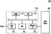
도 7은 본 발명의 실시예에 따른 메모리 시스템을 간략히 보여주는 블록도이다.7 is a simplified block diagram of a memory system in accordance with an embodiment of the present invention.
도 7을 참조하면, 본 발명의 실시예에 따른 메모리 시스템(700)은 불휘발성 메모리 장치(720)와 메모리 컨트롤러(710)를 포함한다.Referring to FIG. 7, a
불휘발성 메모리 장치(720)는 앞서 설명한 반도체 메모리 장치를 포함한다. 메모리 컨트롤러(710)는 불휘발성 메모리 장치(720)를 제어하도록 구성될 것이다. 불휘발성 메모리 장치(720)와 메모리 컨트롤러(710)의 결합에 의해 메모리 카드 또는 반도체 디스크 장치(Solid State Disk: SSD)로 제공될 수 있을 것이다. SRAM(711)은 프로세싱 유닛(712)의 동작 메모리로써 사용된다. 호스트 인터페이스(713)는 메모리 시스템(700)과 접속되는 호스트의 데이터 교환 프로토콜을 구비한다. 에러 정정 블록(714)은 불휘발성 메모리 장치(720)의 셀 영역으로부터 독출된 데이터에 포함되는 에러를 검출 및 정정한다. 메모리 인터페이스(714)는 본 발명의 불휘발성 메모리 장치(720)와 인터페이싱 한다. 프로세싱 유닛(712)은 메모리 컨트롤러(710)의 데이터 교환을 위한 제반 제어 동작을 수행한다.The
비록 도면에는 도시되지 않았지만, 본 발명에 따른 메모리 시스템(700)은 호스트(Host)와의 인터페이싱을 위한 코드 데이터를 저장하는 ROM(미도시됨) 등이 더 제공될 수 있음은 이 분야의 통상적인 지식을 습득한 자들에게 자명하다. 불휘발성 메모리 장치(720)는 복수의 플래시 메모리 칩들로 구성되는 멀티-칩 패키지로 제공될 수도 있다. 이상의 본 발명의 메모리 시스템(700)은 동작 특성이 향상된 고신뢰성의 저장 매체로 제공될 수 있다. 특히, 최근 활발히 연구되고 있는 반도체 디스크 장치(Solid State Disk: 이하 SSD)와 같은 메모리 시스템에서 본 발명의 플래시 메모리 장치가 구비될 수 있다. 이 경우, 메모리 컨트롤러(710)는 USB, MMC, PCI-E, SATA, PATA, SCSI, ESDI, 그리고 IDE 등과 같은 다양한 인터페이스 프로토콜들 중 하나를 통해 외부(예를 들면, 호스트)와 통신하도록 구성될 것이다.Although it is not shown in the drawing, the
도 8은 프로그램 동작을 수행하는 퓨전 메모리 장치 또는 퓨전 메모리 시스템을 간략히 보여주는 블록도이다. 예를 들면, 퓨전 메모리 장치로서 원낸드 플래시 메모리 장치(800)에 본 발명의 기술적 특징이 적용될 수 있다.FIG. 8 is a block diagram schematically illustrating a fusion memory device or a fusion memory system performing a program operation. FIG. For example, the technical features of the present invention can be applied to the one-nAND
원낸드 플래시 메모리 장치(800)는 서로 다른 프로토콜을 사용하는 장치와의 각종 정보 교환을 위한 호스트 인터페이스(810)와, 메모리 장치를 구동하기 위한 코드를 내장하거나 데이터를 일시적으로 저장하는 버퍼 램(820)과, 외부에서 주어지는 제어 신호와 명령어에 응답하여 읽기와 프로그램 및 모든 상태를 제어하는 제어부(830)와, 명령어와 어드레스, 메모리 장치 내부의 시스템 동작 환경을 정의하는 설정(Configuration) 등의 데이터가 저장되는 레지스터(840) 및 불휘발성 메모리 셀과 페이지 버퍼를 포함하는 동작 회로로 구성된 낸드 플래시 셀 어레이(850)를 포함한다. 호스트로부터의 쓰기 요청에 응답하여 원낸드 플래시 메모리 장치는 일반적인 방식에 따라 데이터를 프로그램하게 된다.The NAND
도 9에는 본 발명에 따른 플래시 메모리 장치(912)를 포함한 컴퓨팅 시스템이 개략적으로 도시되어 있다.9, a computing system including a
본 발명에 따른 컴퓨팅 시스템(900)은 시스템 버스(960)에 전기적으로 연결된 마이크로프로세서(920), 램(930), 사용자 인터페이스(940), 베이스밴드 칩셋(Baseband chipset)과 같은 모뎀(950) 및 메모리 시스템(910)을 포함한다. 본 발명에 따른 컴퓨팅 시스템(900)이 모바일 장치인 경우, 컴퓨팅 시스템(900)의 동작 전압을 공급하기 위한 배터리(미도시됨)가 추가적으로 제공될 것이다. 비록 도면에는 도시되지 않았지만, 본 발명에 따른 컴퓨팅 시스템(900)에는 응용 칩셋(Application chipset), 카메라 이미지 프로세서(Camera Image Processor: CIS), 모바일 디램, 등이 더 제공될 수 있음은 이 분야의 통상적인 지식을 습득한 자들에게 자명하다. 메모리 시스템(910)은, 예를 들면, 데이터를 저장하기 위해 도 1에서 설명한 불휘발성 메모리를 사용하는 SSD(Solid State Drive/Disk)를 구성할 수 있다. 또는, 메모리 시스템(910)은, 퓨전 플래시 메모리(예를 들면, 원낸드 플래시 메모리)로 제공될 수 있다.
The
110 : 메모리 어레이110MB : 메모리 블록
120 : 제어 회로130 : 전압 공급 회로
140 : 읽기/쓰기 회로110:
120: control circuit 130: voltage supply circuit
140: Read / write circuit
Claims (18)
Translated fromKorean상기 제1 더미 트랜지스터와 연결되는 제1 선택 트랜지스터;
공통 소스 라인과 연결되는 제2 더미 트랜지스터;
상기 제2 더미 트랜지스터와 연결되는 제2 선택 트랜지스터; 및
상기 제1 및 제2 선택 트랜지스터들 사이에 연결된 메인 셀 트랜지스터들을 포함하는 반도체 메모리 장치.
A first dummy transistor connected to the bit line;
A first selection transistor connected to the first dummy transistor;
A second dummy transistor connected to the common source line;
A second selection transistor connected to the second dummy transistor; And
And main cell transistors coupled between the first and second selection transistors.
상기 제1 선택 트랜지스터와 상기 메인 셀 트랜지스터 사이에 연결된 제1 더미 셀 트랜지스터; 및
상기 제2 선택 트랜지스터와 상기 메인 셀 트랜지스터 사이에 연결된 제2 더미 셀 트랜지스터를 더 포함하는 반도체 메모리 장치.
The method according to claim 1,
A first dummy cell transistor connected between the first select transistor and the main cell transistor; And
And a second dummy cell transistor connected between the second select transistor and the main cell transistor.
상기 셀 트랜지스터들은 기판 상에서 상기 제1 및 제2 선택 트랜지스터들 사이에 수직으로 연결되는 반도체 메모리 장치.
The method according to claim 1,
Wherein the cell transistors are vertically connected between the first and second selection transistors on a substrate.
상기 셀 트랜지스터들이 제1 메인 셀 트랜지스터 그룹과 제2 메인 셀 트랜지스터 그룹으로 구분되고, 상기 제1 및 제2 메인 셀 트랜지스터 그룹들의 사이에 연결된 파이프 트랜지스터를 더 포함하는 반도체 메모리 장치.
The method according to claim 1,
Wherein the cell transistors are divided into a first main cell transistor group and a second main cell transistor group, and a pipe transistor connected between the first and second main cell transistor groups.
상기 제1 선택 트랜지스터와 상기 파이프 트랜지스터 사이에 연결된 상기 제1 메인 셀 트랜지스터 그룹의 상기 메인 셀 트랜지스터들이 기판 상에 수직으로 연결되고,
상기 제2 선택 트랜지스터와 상기 파이프 트랜지스터 사이에 연결된 상기 제2 메인 셀 트랜지스터 그룹의 상기 메인 셀 트랜지스터들이 기판 상에 수직으로 연결되는 반도체 메모리 장치.
5. The method of claim 4,
The main cell transistors of the first main cell transistor group connected between the first select transistor and the pipe transistor are vertically connected to the substrate,
And the main cell transistors of the second main cell transistor group connected between the second selection transistor and the pipe transistor are vertically connected to the substrate.
상기 파이프 트랜지스터 및 상기 제1 메인 셀 트랜지스터 그룹 사이에 접속된 제3 더미 셀 트랜지스터; 및
상기 파이프 트랜지스터 및 상기 제2 메인 셀 트랜지스터 그룹 사이에 접속된 제4 더미 셀 트랜지스터를 더 포함하는 반도체 메모리 장치.
5. The method of claim 4,
A third dummy cell transistor connected between the pipe transistor and the first main cell transistor group; And
And a fourth dummy cell transistor connected between the pipe transistor and the second main cell transistor group.
상기 제1 및 제2 더미 트랜지스터들, 상기 제1 및 제2 선택 트랜지스터들 및 상기 메인 셀 트랜지스터들은 수직 채널층, 상기 수직 채널층을 감싸는 터널 절연막, 상기 터널 절연막을 감싸는 전자 저장막, 상기 전하 저장막을 감싸는 블로킹 절연막 및 상기 블로킹 절연막을 감싸는 도전막을 포함하는 반도체 메모리 장치.
The method according to claim 1,
Wherein the first and second dummy transistors, the first and second selection transistors, and the main cell transistors comprise a vertical channel layer, a tunnel insulating layer surrounding the vertical channel layer, an electron storage layer surrounding the tunnel insulating layer, A blocking insulating film surrounding the film, and a conductive film surrounding the blocking insulating film.
상기 제1 및 제2 더미 트랜지스터들의 상기 수직 채널층들의 불순물 농도가 상기 제1 및 제2 선택 트랜지스터들 또는 상기 메인 셀 트랜지스터들에 포함된 상기 수직 채널층들의 불순물 농도와 다른 반도체 메모리 장치.
8. The method of claim 7,
Wherein an impurity concentration of the vertical channel layers of the first and second dummy transistors is different from an impurity concentration of the vertical channel layers included in the first and second selection transistors or the main cell transistors.
상기 제1 및 제2 더미 트랜지스터들의 상기 수직 채널층들은 문턱전압 조절을 위한 불순물이 도핑된 실리콘막을 포함하는 반도체 메모리 장치.
8. The method of claim 7,
Wherein the vertical channel layers of the first and second dummy transistors comprise an impurity-doped silicon film for threshold voltage adjustment.
상기 제1 및 제2 선택 트랜지스터들 및 상기 메인 셀 트랜지스터들의 프로그램 동작과 상기 메인 셀 트랜지스터들의 리드 동작 및 소거 동작을 수행하도록 구성된 주변 회로를 포함하며,
상기 프로그램 동작 시, 상기 주변 회로는 상기 제1 더미 트랜지스터들을 턴온시키고 상기 제2 더미 트랜지스터들을 턴오프시키도록 구성되는 반도체 메모리 장치.
A plurality of memory strings each including a first dummy transistor connected between a bit line and a common source line, a first select transistor, a main cell transistor, a second select transistor and a second dummy transistor; And
And a peripheral circuit configured to perform a program operation of the first and second selection transistors and the main cell transistors and a read operation and an erase operation of the main cell transistors,
And in the program operation, the peripheral circuit is configured to turn on the first dummy transistors and turn off the second dummy transistors.
상기 제1 및 제2 더미 트랜지스터들, 상기 제1 및 제2 선택 트랜지스터들 및 상기 메인 셀 트랜지스터들은 수직 채널층, 상기 수직 채널층을 감싸는 터널 절연막, 상기 터널 절연막을 감싸는 전자 저장막, 상기 전하 저장막을 감싸는 블로킹 절연막 및 상기 블로킹 절연막을 감싸는 도전막을 포함하는 반도체 메모리 장치.
11. The method of claim 10,
Wherein the first and second dummy transistors, the first and second selection transistors, and the main cell transistors comprise a vertical channel layer, a tunnel insulating layer surrounding the vertical channel layer, an electron storage layer surrounding the tunnel insulating layer, A blocking insulating film surrounding the film, and a conductive film surrounding the blocking insulating film.
상기 제1 및 제2 더미 트랜지스터들의 문턱전압들은 상기 제1 및 제2 더미 트랜지스터들의 채널층에 주입된 불순물들에 의해 문턱전압이 결정되고,
상기 제1 및 제2 선택 트랜지스터들 및 상기 메인 셀 트랜지스터들의 문턱전압들은 상기 주변 회로의 상기 프로그램 동작에 의해 결정되는 반도체 메모리 장치.
11. The method of claim 10,
Threshold voltages of the first and second dummy transistors are determined by impurities injected into the channel layers of the first and second dummy transistors,
Threshold voltages of the first and second selection transistors and the main cell transistors are determined by the programming operation of the peripheral circuit.
상기 주변 회로는 상기 제1 및 제2 선택 트랜지스터들의 문턱전압들을 데이터에 상관없이 정해진 레벨까지 상승시키기 위하여 상기 제1 및 제2 선택 트랜지스터들의 상기 프로그램 동작을 실시하는 반도체 메모리 장치.
11. The method of claim 10,
Wherein the peripheral circuit performs the programming operation of the first and second selection transistors to raise the threshold voltages of the first and second selection transistors to a predetermined level regardless of data.
상기 제1 선택 트랜지스터들의 프로그램 동작 시, 문턱전압이 목표 레벨보다 높은 제1 선택 트랜지스터의 프로그램 금지를 위해, 상기 주변 회로는 상기 비트 라인과 상기 제1 더미 트랜지스터에 프로그램 금지 전압을 인가하도록 구성되는 반도체 메모리 장치.
11. The method of claim 10,
Wherein the peripheral circuitry is configured to apply a program inhibit voltage to the bit line and the first dummy transistor for program inhibition of a first select transistor having a threshold voltage higher than a target level during a programming operation of the first select transistors. Memory device.
상기 주변 회로는 상기 제1 선택 트랜지스터의 프로그램 동작과 상기 제2 선택 트랜지스터의 프로그램 동작을 동시에 실시하는 반도체 메모리 장치.
11. The method of claim 10,
Wherein said peripheral circuit simultaneously performs a program operation of said first select transistor and a program operation of said second select transistor.
상기 메인 셀 트랜지스터들의 상기 리드 동작 시, 상기 주변 회로는 상기 제1 및 제2 더미 트랜지스터들에 리드 패스 전압을 인가하도록 구성되는 반도체 메모리 장치.
11. The method of claim 10,
And in the read operation of the main cell transistors, the peripheral circuit is configured to apply a read pass voltage to the first and second dummy transistors.
상기 메인 셀 트랜지스터들의 상기 소거 동작 시, 상기 주변 회로는 상기 제1 및 제2 더미 트랜지스터들의 게이트들을 플로팅 상태로 설정하도록 구성되는 반도체 메모리 장치.
11. The method of claim 10,
And in the erase operation of the main cell transistors, the peripheral circuit is configured to set the gates of the first and second dummy transistors in a floating state.
상기 제1 선택 트랜지스터와 상기 메인 셀 트랜지스터 사이에 연결된 제1 더미 셀 트랜지스터; 및
상기 제2 선택 트랜지스터와 상기 메인 셀 트랜지스터 사이에 연결된 제2 더미 셀 트랜지스터를 더 포함하는 반도체 메모리 장치.11. The method of claim 10,
A first dummy cell transistor connected between the first select transistor and the main cell transistor; And
And a second dummy cell transistor connected between the second select transistor and the main cell transistor.
Priority Applications (2)
| Application Number | Priority Date | Filing Date | Title |
|---|---|---|---|
| KR20130051173AKR20140132102A (en) | 2013-05-07 | 2013-05-07 | Semiconductor memory apparatus and method of operating the same |
| US13/958,201US9171861B2 (en) | 2013-05-07 | 2013-08-02 | Semiconductor memory device and system having the same |
Applications Claiming Priority (1)
| Application Number | Priority Date | Filing Date | Title |
|---|---|---|---|
| KR20130051173AKR20140132102A (en) | 2013-05-07 | 2013-05-07 | Semiconductor memory apparatus and method of operating the same |
Publications (1)
| Publication Number | Publication Date |
|---|---|
| KR20140132102Atrue KR20140132102A (en) | 2014-11-17 |
Family
ID=51864672
Family Applications (1)
| Application Number | Title | Priority Date | Filing Date |
|---|---|---|---|
| KR20130051173AWithdrawnKR20140132102A (en) | 2013-05-07 | 2013-05-07 | Semiconductor memory apparatus and method of operating the same |
Country Status (2)
| Country | Link |
|---|---|
| US (1) | US9171861B2 (en) |
| KR (1) | KR20140132102A (en) |
Cited By (3)
| Publication number | Priority date | Publication date | Assignee | Title |
|---|---|---|---|---|
| KR20170086746A (en)* | 2016-01-18 | 2017-07-27 | 삼성전자주식회사 | Memory device |
| US9892801B2 (en) | 2015-07-20 | 2018-02-13 | SK Hynix Inc. | Semiconductor memory device with improved program verification reliability |
| KR20200078163A (en)* | 2018-12-21 | 2020-07-01 | 에스케이하이닉스 주식회사 | Semiconductor device and manufacturing method of a semiconductor device |
Families Citing this family (24)
| Publication number | Priority date | Publication date | Assignee | Title |
|---|---|---|---|---|
| US9276011B2 (en) | 2013-03-15 | 2016-03-01 | Micron Technology, Inc. | Cell pillar structures and integrated flows |
| US9472291B2 (en)* | 2013-05-16 | 2016-10-18 | SK Hynix Inc. | Semiconductor memory device and method of operating the same |
| KR20150026209A (en)* | 2013-09-02 | 2015-03-11 | 삼성전자주식회사 | Vertical memory devices and methods of manufacturing the same |
| JP2015060602A (en)* | 2013-09-17 | 2015-03-30 | 株式会社東芝 | Nonvolatile semiconductor memory device |
| US9437604B2 (en) | 2013-11-01 | 2016-09-06 | Micron Technology, Inc. | Methods and apparatuses having strings of memory cells including a metal source |
| US9431410B2 (en) | 2013-11-01 | 2016-08-30 | Micron Technology, Inc. | Methods and apparatuses having memory cells including a monolithic semiconductor channel |
| US10276562B2 (en) | 2014-01-07 | 2019-04-30 | Taiwan Semiconductor Manufacturing Co., Ltd. | Semiconductor device with multiple threshold voltage and method of fabricating the same |
| CN106463534B (en)* | 2014-06-23 | 2020-12-11 | 英特尔公司 | Techniques for Forming Vertical Transistor Architectures |
| KR20160029506A (en)* | 2014-09-05 | 2016-03-15 | 에스케이하이닉스 주식회사 | Semiconductor memory device including 3-dimensional memory cell array and operating method thereof |
| US9251909B1 (en)* | 2014-09-29 | 2016-02-02 | International Business Machines Corporation | Background threshold voltage shifting using base and delta threshold voltage shift values in flash memory |
| KR20160062498A (en) | 2014-11-25 | 2016-06-02 | 에스케이하이닉스 주식회사 | Semiconductor memory device and operating method thereof |
| KR20160107553A (en)* | 2015-03-04 | 2016-09-19 | 에스케이하이닉스 주식회사 | Semiconductor apparatus |
| KR20160139991A (en)* | 2015-05-29 | 2016-12-07 | 에스케이하이닉스 주식회사 | Semiconductor device and operating method thereof |
| KR102345597B1 (en) | 2015-06-30 | 2022-01-03 | 삼성전자주식회사 | 3 dimensional flash memory device comprising dummy word line |
| US10707121B2 (en)* | 2016-12-31 | 2020-07-07 | Intel Corporatino | Solid state memory device, and manufacturing method thereof |
| JP2019160380A (en) | 2018-03-16 | 2019-09-19 | 東芝メモリ株式会社 | Semiconductor storage device |
| KR102671195B1 (en)* | 2018-12-28 | 2024-06-03 | 에스케이하이닉스 주식회사 | Semiconductor device and manufacturing method of a semiconductor device |
| KR102666991B1 (en) | 2019-02-14 | 2024-05-20 | 에스케이하이닉스 주식회사 | Semiconductor device and manufacturing method of a semiconductor device |
| KR102691258B1 (en)* | 2019-03-21 | 2024-08-01 | 삼성전자주식회사 | Nonvoltile memory device and erase method thereof |
| US11476267B2 (en)* | 2019-05-24 | 2022-10-18 | Applied Materials, Inc. | Liner for V-NAND word line stack |
| CN113196402B (en) | 2020-03-23 | 2022-11-04 | 长江存储科技有限责任公司 | Memory devices and their programming operations |
| CN111527544B (en)* | 2020-03-23 | 2021-04-16 | 长江存储科技有限责任公司 | How to operate 3D NAND flash memory and 3D NAND flash memory |
| JP2023001828A (en)* | 2021-06-21 | 2023-01-06 | キオクシア株式会社 | semiconductor storage device |
| US12419051B2 (en)* | 2022-07-12 | 2025-09-16 | SK Hynix Inc. | Semiconductor memory device and manufacturing method of semiconductor memory device |
Family Cites Families (3)
| Publication number | Priority date | Publication date | Assignee | Title |
|---|---|---|---|---|
| JP4005895B2 (en)* | 2002-09-30 | 2007-11-14 | 株式会社東芝 | Nonvolatile semiconductor memory device |
| JP5142692B2 (en)* | 2007-12-11 | 2013-02-13 | 株式会社東芝 | Nonvolatile semiconductor memory device |
| KR20120088360A (en) | 2011-01-31 | 2012-08-08 | 삼성전자주식회사 | Operating method of nonvolatile memory device |
- 2013
- 2013-05-07KRKR20130051173Apatent/KR20140132102A/ennot_activeWithdrawn
- 2013-08-02USUS13/958,201patent/US9171861B2/enactiveActive
Cited By (3)
| Publication number | Priority date | Publication date | Assignee | Title |
|---|---|---|---|---|
| US9892801B2 (en) | 2015-07-20 | 2018-02-13 | SK Hynix Inc. | Semiconductor memory device with improved program verification reliability |
| KR20170086746A (en)* | 2016-01-18 | 2017-07-27 | 삼성전자주식회사 | Memory device |
| KR20200078163A (en)* | 2018-12-21 | 2020-07-01 | 에스케이하이닉스 주식회사 | Semiconductor device and manufacturing method of a semiconductor device |
Also Published As
| Publication number | Publication date |
|---|---|
| US9171861B2 (en) | 2015-10-27 |
| US20140334230A1 (en) | 2014-11-13 |
Similar Documents
| Publication | Publication Date | Title |
|---|---|---|
| KR20140132102A (en) | Semiconductor memory apparatus and method of operating the same | |
| US10147731B2 (en) | Semiconductor device | |
| JP5788183B2 (en) | Nonvolatile memory device, method of operating the same, and memory system including the same | |
| US9484099B2 (en) | Three dimensional semiconductor memory device with line sharing scheme | |
| US9053794B2 (en) | Nonvolatile memory device and related method of operation | |
| US9875800B2 (en) | 3D NAND semiconductor device for erasing groups of bit lines | |
| KR101997912B1 (en) | Semiconductor memory device and method of operating the same | |
| KR102222594B1 (en) | Nonvolatile memory device, erasing method thereof and memory system including the same | |
| KR20150014680A (en) | Semiconductor memory apparatus | |
| TWI633554B (en) | Semiconductor device | |
| US9330771B2 (en) | Semiconductor device | |
| US9633737B2 (en) | Semiconductor device | |
| US9564223B2 (en) | Semiconductor device | |
| US10529429B2 (en) | Semiconductor memory device and method of operating the same | |
| KR20110095104A (en) | Nonvolatile Memory Device, Its Operation Method, and Memory System Including It | |
| KR20140135402A (en) | Semiconductor memory device and operating method thereof | |
| KR20160061765A (en) | Semiconductor apparatus | |
| KR20160043747A (en) | Semiconductor apparatus | |
| US9330780B1 (en) | Semiconductor device including a memory block and method of operating the same | |
| KR20160050656A (en) | Semiconductor apparatus | |
| KR20160069378A (en) | Semiconductor apparatus |
Legal Events
| Date | Code | Title | Description |
|---|---|---|---|
| PA0109 | Patent application | Patent event code:PA01091R01D Comment text:Patent Application Patent event date:20130507 | |
| PG1501 | Laying open of application | ||
| PC1203 | Withdrawal of no request for examination | ||
| WITN | Application deemed withdrawn, e.g. because no request for examination was filed or no examination fee was paid |