KR20140130666A - Near unity power factor long life low cost led lamp retrofit system and method - Google Patents
Near unity power factor long life low cost led lamp retrofit system and methodDownload PDFInfo
- Publication number
- KR20140130666A KR20140130666AKR1020147019903AKR20147019903AKR20140130666AKR 20140130666 AKR20140130666 AKR 20140130666AKR 1020147019903 AKR1020147019903 AKR 1020147019903AKR 20147019903 AKR20147019903 AKR 20147019903AKR 20140130666 AKR20140130666 AKR 20140130666A
- Authority
- KR
- South Korea
- Prior art keywords
- led
- coupled
- circuit
- voltage
- lamp
- Prior art date
- Legal status (The legal status is an assumption and is not a legal conclusion. Google has not performed a legal analysis and makes no representation as to the accuracy of the status listed.)
- Withdrawn
Links
- 238000000034methodMethods0.000titleclaimsdescription164
- 229910052736halogenInorganic materials0.000claimsabstractdescription60
- 150000002367halogensChemical class0.000claimsabstractdescription58
- DGAQECJNVWCQMB-PUAWFVPOSA-MIlexoside XXIXChemical compoundC[C@@H]1CC[C@@]2(CC[C@@]3(C(=CC[C@H]4[C@]3(CC[C@@H]5[C@@]4(CC[C@@H](C5(C)C)OS(=O)(=O)[O-])C)C)[C@@H]2[C@]1(C)O)C)C(=O)O[C@H]6[C@@H]([C@H]([C@@H]([C@H](O6)CO)O)O)O.[Na+]DGAQECJNVWCQMB-PUAWFVPOSA-M0.000claimsabstractdescription36
- 229910052708sodiumInorganic materials0.000claimsabstractdescription36
- 239000011734sodiumSubstances0.000claimsabstractdescription36
- 238000009429electrical wiringMethods0.000claimsabstractdescription27
- 239000003990capacitorSubstances0.000claimsdescription279
- 239000000872bufferSubstances0.000claimsdescription114
- 238000001914filtrationMethods0.000claimsdescription88
- 101100524516Saccharomyces cerevisiae (strain ATCC 204508 / S288c) RFA2 geneProteins0.000claimsdescription35
- 230000003287optical effectEffects0.000claimsdescription29
- 238000002955isolationMethods0.000claimsdescription25
- 238000012546transferMethods0.000claimsdescription23
- 101100033865Saccharomyces cerevisiae (strain ATCC 204508 / S288c) RFA1 geneProteins0.000claimsdescription20
- 229910052751metalInorganic materials0.000claimsdescription20
- 239000002184metalSubstances0.000claimsdescription20
- 230000000670limiting effectEffects0.000claimsdescription18
- 238000009413insulationMethods0.000claimsdescription17
- 230000002829reductive effectEffects0.000claimsdescription14
- 230000000903blocking effectEffects0.000claimsdescription13
- 230000000694effectsEffects0.000claimsdescription10
- 230000008878couplingEffects0.000claimsdescription9
- 238000010168coupling processMethods0.000claimsdescription9
- 238000005859coupling reactionMethods0.000claimsdescription9
- 238000001514detection methodMethods0.000claimsdescription5
- 230000005855radiationEffects0.000claimsdescription5
- 230000015556catabolic processEffects0.000claimsdescription3
- 230000003247decreasing effectEffects0.000claims1
- 238000009792diffusion processMethods0.000abstractdescription20
- 230000003993interactionEffects0.000abstract1
- 239000000306componentSubstances0.000description119
- 230000008901benefitEffects0.000description62
- 238000013461designMethods0.000description29
- 238000005516engineering processMethods0.000description28
- 238000013459approachMethods0.000description23
- 230000006870functionEffects0.000description22
- 238000010586diagramMethods0.000description21
- 238000012986modificationMethods0.000description21
- 230000004048modificationEffects0.000description21
- 239000011521glassSubstances0.000description19
- 238000011084recoveryMethods0.000description19
- 239000007858starting materialSubstances0.000description18
- 238000004519manufacturing processMethods0.000description17
- 238000005868electrolysis reactionMethods0.000description15
- 230000008569processEffects0.000description15
- 239000004065semiconductorSubstances0.000description14
- 238000012937correctionMethods0.000description11
- 238000005286illuminationMethods0.000description11
- 230000001105regulatory effectEffects0.000description11
- 230000007423decreaseEffects0.000description8
- 230000006872improvementEffects0.000description8
- 239000004033plasticSubstances0.000description8
- 230000002441reversible effectEffects0.000description8
- 230000001276controlling effectEffects0.000description7
- 230000005611electricityEffects0.000description7
- 230000010354integrationEffects0.000description7
- 229910052710siliconInorganic materials0.000description7
- 239000010703siliconSubstances0.000description7
- XUIMIQQOPSSXEZ-UHFFFAOYSA-NSiliconChemical compound[Si]XUIMIQQOPSSXEZ-UHFFFAOYSA-N0.000description6
- 229910052782aluminiumInorganic materials0.000description6
- XAGFODPZIPBFFR-UHFFFAOYSA-NaluminiumChemical compound[Al]XAGFODPZIPBFFR-UHFFFAOYSA-N0.000description6
- 230000009977dual effectEffects0.000description6
- 239000000463materialSubstances0.000description6
- 101150030566CCS1 geneProteins0.000description5
- 101100332461Coffea arabica DXMT2 geneProteins0.000description5
- 101100341123Saccharomyces cerevisiae (strain ATCC 204508 / S288c) IRA2 geneProteins0.000description5
- 101150104736ccsB geneProteins0.000description5
- 238000006243chemical reactionMethods0.000description5
- 238000000576coating methodMethods0.000description5
- 238000009826distributionMethods0.000description5
- 239000007787solidSubstances0.000description5
- 229910052721tungstenInorganic materials0.000description5
- 239000010937tungstenSubstances0.000description5
- 238000004364calculation methodMethods0.000description4
- 239000007789gasSubstances0.000description4
- 238000003780insertionMethods0.000description4
- 230000037431insertionEffects0.000description4
- 230000010355oscillationEffects0.000description4
- 230000035939shockEffects0.000description4
- 238000001228spectrumMethods0.000description4
- WFKWXMTUELFFGS-UHFFFAOYSA-NtungstenChemical compound[W]WFKWXMTUELFFGS-UHFFFAOYSA-N0.000description4
- 241001085205Prenanthella exiguaSpecies0.000description3
- 239000011248coating agentSubstances0.000description3
- 239000002131composite materialSubstances0.000description3
- 238000010276constructionMethods0.000description3
- 101150069022dss-1 geneProteins0.000description3
- QSHDDOUJBYECFT-UHFFFAOYSA-NmercuryChemical compound[Hg]QSHDDOUJBYECFT-UHFFFAOYSA-N0.000description3
- 238000004806packaging method and processMethods0.000description3
- 230000009467reductionEffects0.000description3
- 238000001429visible spectrumMethods0.000description3
- ZCYVEMRRCGMTRW-UHFFFAOYSA-N7553-56-2Chemical compound[I]ZCYVEMRRCGMTRW-UHFFFAOYSA-N0.000description2
- 230000003466anti-cipated effectEffects0.000description2
- 230000006399behaviorEffects0.000description2
- 230000033228biological regulationEffects0.000description2
- 239000011449brickSubstances0.000description2
- 230000003139buffering effectEffects0.000description2
- 239000003086colorantSubstances0.000description2
- 230000002860competitive effectEffects0.000description2
- 239000000470constituentSubstances0.000description2
- 239000000428dustSubstances0.000description2
- 238000010292electrical insulationMethods0.000description2
- 230000007613environmental effectEffects0.000description2
- 239000011261inert gasSubstances0.000description2
- 238000009434installationMethods0.000description2
- 239000012774insulation materialSubstances0.000description2
- 229910052740iodineInorganic materials0.000description2
- 239000011630iodineSubstances0.000description2
- 230000033001locomotionEffects0.000description2
- 230000007257malfunctionEffects0.000description2
- 229910052753mercuryInorganic materials0.000description2
- 239000003607modifierSubstances0.000description2
- 238000000465mouldingMethods0.000description2
- 230000000737periodic effectEffects0.000description2
- 230000001737promoting effectEffects0.000description2
- 238000004064recyclingMethods0.000description2
- 238000003860storageMethods0.000description2
- 229920003002synthetic resinPolymers0.000description2
- 239000000057synthetic resinSubstances0.000description2
- 229910052720vanadiumInorganic materials0.000description2
- WKBOTKDWSSQWDR-UHFFFAOYSA-NBromine atomChemical compound[Br]WKBOTKDWSSQWDR-UHFFFAOYSA-N0.000description1
- 241001621399LamprisSpecies0.000description1
- OAICVXFJPJFONN-UHFFFAOYSA-NPhosphorusChemical compound[P]OAICVXFJPJFONN-UHFFFAOYSA-N0.000description1
- 238000012356Product developmentMethods0.000description1
- BQCADISMDOOEFD-UHFFFAOYSA-NSilverChemical compound[Ag]BQCADISMDOOEFD-UHFFFAOYSA-N0.000description1
- 230000003213activating effectEffects0.000description1
- 230000002411adverseEffects0.000description1
- 239000000956alloySubstances0.000description1
- 229910045601alloyInorganic materials0.000description1
- 238000003339best practiceMethods0.000description1
- 230000005540biological transmissionEffects0.000description1
- GDTBXPJZTBHREO-UHFFFAOYSA-NbromineSubstancesBrBrGDTBXPJZTBHREO-UHFFFAOYSA-N0.000description1
- 229910052794bromiumInorganic materials0.000description1
- 229910052793cadmiumInorganic materials0.000description1
- BDOSMKKIYDKNTQ-UHFFFAOYSA-Ncadmium atomChemical compound[Cd]BDOSMKKIYDKNTQ-UHFFFAOYSA-N0.000description1
- 230000008859changeEffects0.000description1
- 238000004891communicationMethods0.000description1
- 230000000052comparative effectEffects0.000description1
- 230000000295complement effectEffects0.000description1
- 238000005094computer simulationMethods0.000description1
- 239000004020conductorSubstances0.000description1
- 238000011217control strategyMethods0.000description1
- 238000001816coolingMethods0.000description1
- 239000008358core componentSubstances0.000description1
- 230000001186cumulative effectEffects0.000description1
- 230000002354daily effectEffects0.000description1
- 230000000593degrading effectEffects0.000description1
- 230000000881depressing effectEffects0.000description1
- 238000011161developmentMethods0.000description1
- 238000007599dischargingMethods0.000description1
- 238000000295emission spectrumMethods0.000description1
- 238000005265energy consumptionMethods0.000description1
- 238000003912environmental pollutionMethods0.000description1
- 238000012053enzymatic serum creatinine assayMethods0.000description1
- 238000011156evaluationMethods0.000description1
- 230000003203everyday effectEffects0.000description1
- 238000009472formulationMethods0.000description1
- 238000007710freezingMethods0.000description1
- 230000008014freezingEffects0.000description1
- 239000000446fuelSubstances0.000description1
- 231100001261hazardousToxicity0.000description1
- 239000002920hazardous wasteSubstances0.000description1
- 230000000415inactivating effectEffects0.000description1
- 239000012212insulatorSubstances0.000description1
- 230000002452interceptive effectEffects0.000description1
- 235000000396ironNutrition0.000description1
- 230000002427irreversible effectEffects0.000description1
- 239000011159matrix materialSubstances0.000description1
- 238000002844meltingMethods0.000description1
- 230000008018meltingEffects0.000description1
- 239000000203mixtureSubstances0.000description1
- 229910052754neonInorganic materials0.000description1
- GKAOGPIIYCISHV-UHFFFAOYSA-Nneon atomChemical compound[Ne]GKAOGPIIYCISHV-UHFFFAOYSA-N0.000description1
- 210000005036nerveAnatomy0.000description1
- 238000013021overheatingMethods0.000description1
- 230000003647oxidationEffects0.000description1
- 238000007254oxidation reactionMethods0.000description1
- TWNQGVIAIRXVLR-UHFFFAOYSA-Noxo(oxoalumanyloxy)alumaneChemical compoundO=[Al]O[Al]=OTWNQGVIAIRXVLR-UHFFFAOYSA-N0.000description1
- 230000036961partial effectEffects0.000description1
- 231100000614poisonToxicity0.000description1
- 238000002360preparation methodMethods0.000description1
- 230000001681protective effectEffects0.000description1
- 239000010453quartzSubstances0.000description1
- 238000011160researchMethods0.000description1
- 238000012827research and developmentMethods0.000description1
- 238000012552reviewMethods0.000description1
- 238000010079rubber tappingMethods0.000description1
- 230000035945sensitivityEffects0.000description1
- VYPSYNLAJGMNEJ-UHFFFAOYSA-Nsilicon dioxideInorganic materialsO=[Si]=OVYPSYNLAJGMNEJ-UHFFFAOYSA-N0.000description1
- 229910052709silverInorganic materials0.000description1
- 239000004332silverSubstances0.000description1
- 239000003381stabilizerSubstances0.000description1
- 230000000087stabilizing effectEffects0.000description1
- 239000000758substrateSubstances0.000description1
- 230000001360synchronised effectEffects0.000description1
- 238000012360testing methodMethods0.000description1
- 239000003440toxic substanceSubstances0.000description1
- 230000001052transient effectEffects0.000description1
- 239000012780transparent materialSubstances0.000description1
- -1tungsten halogenChemical class0.000description1
- 238000009827uniform distributionMethods0.000description1
- 238000009423ventilationMethods0.000description1
- 238000010792warmingMethods0.000description1
- XLYOFNOQVPJJNP-UHFFFAOYSA-NwaterSubstancesOXLYOFNOQVPJJNP-UHFFFAOYSA-N0.000description1
- 238000004804windingMethods0.000description1
Images


Classifications
- H—ELECTRICITY
- H05—ELECTRIC TECHNIQUES NOT OTHERWISE PROVIDED FOR
- H05B—ELECTRIC HEATING; ELECTRIC LIGHT SOURCES NOT OTHERWISE PROVIDED FOR; CIRCUIT ARRANGEMENTS FOR ELECTRIC LIGHT SOURCES, IN GENERAL
- H05B45/00—Circuit arrangements for operating light-emitting diodes [LED]
- H05B45/30—Driver circuits
- H05B45/357—Driver circuits specially adapted for retrofit LED light sources
- H05B45/3578—Emulating the electrical or functional characteristics of discharge lamps
- F—MECHANICAL ENGINEERING; LIGHTING; HEATING; WEAPONS; BLASTING
- F21—LIGHTING
- F21K—NON-ELECTRIC LIGHT SOURCES USING LUMINESCENCE; LIGHT SOURCES USING ELECTROCHEMILUMINESCENCE; LIGHT SOURCES USING CHARGES OF COMBUSTIBLE MATERIAL; LIGHT SOURCES USING SEMICONDUCTOR DEVICES AS LIGHT-GENERATING ELEMENTS; LIGHT SOURCES NOT OTHERWISE PROVIDED FOR
- F21K9/00—Light sources using semiconductor devices as light-generating elements, e.g. using light-emitting diodes [LED] or lasers
- F21K9/20—Light sources comprising attachment means
- F21K9/23—Retrofit light sources for lighting devices with a single fitting for each light source, e.g. for substitution of incandescent lamps with bayonet or threaded fittings
- F21K9/232—Retrofit light sources for lighting devices with a single fitting for each light source, e.g. for substitution of incandescent lamps with bayonet or threaded fittings specially adapted for generating an essentially omnidirectional light distribution, e.g. with a glass bulb
- H—ELECTRICITY
- H05—ELECTRIC TECHNIQUES NOT OTHERWISE PROVIDED FOR
- H05B—ELECTRIC HEATING; ELECTRIC LIGHT SOURCES NOT OTHERWISE PROVIDED FOR; CIRCUIT ARRANGEMENTS FOR ELECTRIC LIGHT SOURCES, IN GENERAL
- H05B45/00—Circuit arrangements for operating light-emitting diodes [LED]
- H05B45/30—Driver circuits
- H05B45/355—Power factor correction [PFC]; Reactive power compensation
- H—ELECTRICITY
- H05—ELECTRIC TECHNIQUES NOT OTHERWISE PROVIDED FOR
- H05B—ELECTRIC HEATING; ELECTRIC LIGHT SOURCES NOT OTHERWISE PROVIDED FOR; CIRCUIT ARRANGEMENTS FOR ELECTRIC LIGHT SOURCES, IN GENERAL
- H05B45/00—Circuit arrangements for operating light-emitting diodes [LED]
- H05B45/30—Driver circuits
- H05B45/357—Driver circuits specially adapted for retrofit LED light sources
- H05B45/3574—Emulating the electrical or functional characteristics of incandescent lamps
- H—ELECTRICITY
- H05—ELECTRIC TECHNIQUES NOT OTHERWISE PROVIDED FOR
- H05B—ELECTRIC HEATING; ELECTRIC LIGHT SOURCES NOT OTHERWISE PROVIDED FOR; CIRCUIT ARRANGEMENTS FOR ELECTRIC LIGHT SOURCES, IN GENERAL
- H05B45/00—Circuit arrangements for operating light-emitting diodes [LED]
- H05B45/30—Driver circuits
- H05B45/37—Converter circuits
- H05B45/3725—Switched mode power supply [SMPS]
- H05B45/38—Switched mode power supply [SMPS] using boost topology
- H—ELECTRICITY
- H05—ELECTRIC TECHNIQUES NOT OTHERWISE PROVIDED FOR
- H05B—ELECTRIC HEATING; ELECTRIC LIGHT SOURCES NOT OTHERWISE PROVIDED FOR; CIRCUIT ARRANGEMENTS FOR ELECTRIC LIGHT SOURCES, IN GENERAL
- H05B45/00—Circuit arrangements for operating light-emitting diodes [LED]
- H05B45/30—Driver circuits
- H05B45/37—Converter circuits
- H05B45/3725—Switched mode power supply [SMPS]
- H05B45/382—Switched mode power supply [SMPS] with galvanic isolation between input and output
- H—ELECTRICITY
- H05—ELECTRIC TECHNIQUES NOT OTHERWISE PROVIDED FOR
- H05B—ELECTRIC HEATING; ELECTRIC LIGHT SOURCES NOT OTHERWISE PROVIDED FOR; CIRCUIT ARRANGEMENTS FOR ELECTRIC LIGHT SOURCES, IN GENERAL
- H05B45/00—Circuit arrangements for operating light-emitting diodes [LED]
- H05B45/30—Driver circuits
- H05B45/37—Converter circuits
- H05B45/3725—Switched mode power supply [SMPS]
- H05B45/385—Switched mode power supply [SMPS] using flyback topology
- H—ELECTRICITY
- H05—ELECTRIC TECHNIQUES NOT OTHERWISE PROVIDED FOR
- H05B—ELECTRIC HEATING; ELECTRIC LIGHT SOURCES NOT OTHERWISE PROVIDED FOR; CIRCUIT ARRANGEMENTS FOR ELECTRIC LIGHT SOURCES, IN GENERAL
- H05B45/00—Circuit arrangements for operating light-emitting diodes [LED]
- H05B45/40—Details of LED load circuits
- H05B45/44—Details of LED load circuits with an active control inside an LED matrix
- H05B45/46—Details of LED load circuits with an active control inside an LED matrix having LEDs disposed in parallel lines
- H—ELECTRICITY
- H05—ELECTRIC TECHNIQUES NOT OTHERWISE PROVIDED FOR
- H05B—ELECTRIC HEATING; ELECTRIC LIGHT SOURCES NOT OTHERWISE PROVIDED FOR; CIRCUIT ARRANGEMENTS FOR ELECTRIC LIGHT SOURCES, IN GENERAL
- H05B45/00—Circuit arrangements for operating light-emitting diodes [LED]
- H05B45/40—Details of LED load circuits
- H05B45/44—Details of LED load circuits with an active control inside an LED matrix
- H05B45/48—Details of LED load circuits with an active control inside an LED matrix having LEDs organised in strings and incorporating parallel shunting devices
- H—ELECTRICITY
- H05—ELECTRIC TECHNIQUES NOT OTHERWISE PROVIDED FOR
- H05B—ELECTRIC HEATING; ELECTRIC LIGHT SOURCES NOT OTHERWISE PROVIDED FOR; CIRCUIT ARRANGEMENTS FOR ELECTRIC LIGHT SOURCES, IN GENERAL
- H05B45/00—Circuit arrangements for operating light-emitting diodes [LED]
- H05B45/50—Circuit arrangements for operating light-emitting diodes [LED] responsive to malfunctions or undesirable behaviour of LEDs; responsive to LED life; Protective circuits
- H05B45/59—Circuit arrangements for operating light-emitting diodes [LED] responsive to malfunctions or undesirable behaviour of LEDs; responsive to LED life; Protective circuits for reducing or suppressing flicker or glow effects
- H—ELECTRICITY
- H05—ELECTRIC TECHNIQUES NOT OTHERWISE PROVIDED FOR
- H05B—ELECTRIC HEATING; ELECTRIC LIGHT SOURCES NOT OTHERWISE PROVIDED FOR; CIRCUIT ARRANGEMENTS FOR ELECTRIC LIGHT SOURCES, IN GENERAL
- H05B45/00—Circuit arrangements for operating light-emitting diodes [LED]
- H05B45/30—Driver circuits
- H05B45/37—Converter circuits
- H05B45/3725—Switched mode power supply [SMPS]
- H—ELECTRICITY
- H05—ELECTRIC TECHNIQUES NOT OTHERWISE PROVIDED FOR
- H05B—ELECTRIC HEATING; ELECTRIC LIGHT SOURCES NOT OTHERWISE PROVIDED FOR; CIRCUIT ARRANGEMENTS FOR ELECTRIC LIGHT SOURCES, IN GENERAL
- H05B45/00—Circuit arrangements for operating light-emitting diodes [LED]
- H05B45/30—Driver circuits
- H05B45/395—Linear regulators
- Y—GENERAL TAGGING OF NEW TECHNOLOGICAL DEVELOPMENTS; GENERAL TAGGING OF CROSS-SECTIONAL TECHNOLOGIES SPANNING OVER SEVERAL SECTIONS OF THE IPC; TECHNICAL SUBJECTS COVERED BY FORMER USPC CROSS-REFERENCE ART COLLECTIONS [XRACs] AND DIGESTS
- Y02—TECHNOLOGIES OR APPLICATIONS FOR MITIGATION OR ADAPTATION AGAINST CLIMATE CHANGE
- Y02B—CLIMATE CHANGE MITIGATION TECHNOLOGIES RELATED TO BUILDINGS, e.g. HOUSING, HOUSE APPLIANCES OR RELATED END-USER APPLICATIONS
- Y02B20/00—Energy efficient lighting technologies, e.g. halogen lamps or gas discharge lamps
- Y02B20/30—Semiconductor lamps, e.g. solid state lamps [SSL] light emitting diodes [LED] or organic LED [OLED]
Landscapes
- Engineering & Computer Science (AREA)
- Physics & Mathematics (AREA)
- Microelectronics & Electronic Packaging (AREA)
- Optics & Photonics (AREA)
- General Engineering & Computer Science (AREA)
- Circuit Arrangement For Electric Light Sources In General (AREA)
- Led Devices (AREA)
Abstract
Translated fromKorean
Description
Translated fromKorean관련 출원에 대한 참조Reference to Related Application
본 출원은 2011년 12월 16일에 출원된 US 가출원 특허 제61/576,604호《고역률 내구성 저비용 LED 램프 개조형 시스템 및 방법》과 2012년 10월 5일에 출원된 US 가출원 특허 제61/710,286호《고역률 내구성 저비용 LED 램프 개조 시스템 및 방법》의 특혜를 청구하며 매개 출원은 그 전체를 여기에 참조로 합체하였다.The present application is related to U.S. Provisional Patent Application No. 61 / 576,604 entitled " High Power Factor Durability Low Cost LED Lamp Correction Type System and Method ", filed December 16, 2011, and U.S. Provisional Patent Application Serial No. 61 / 710,286 filed October 5, The present application claims the benefit of "High Power Factor Durability Low Cost LED Lamp Reconditioning System and Method", the entirety of which is hereby incorporated by reference.
1. 기술분야1. Technical Field
여기에 개시된 다양한 실시예들은 넓은 범위의 전력에서 동작할 수 있고 백열등, 할로겐, 나트륨 또는 형광 램프와 같은 종래의 조명 장치들을 대신할 수 있는 저비용 고품질 LED(발광 다이오드) 개조형 램프 장치에 관한 것이다.The various embodiments disclosed herein are directed to a low cost, high quality LED (light emitting diode) modulating lamp device that can operate over a wide range of power and replace conventional lighting devices such as incandescent, halogen, sodium or fluorescent lamps.
보다 구체적으로는, 여기에 개시된 실시예들은 LED, LED 패널, 급전 어댑터, 하우징, 렌즈/확산 차폐막, In/Out 전기 배선과 LED 드라이버와 같은 일곱 개의 상호작용 시스템의 전기-기계-광학 호환성을 최대화하는 LED 램프 개조형 장치에 관한 것이다.More specifically, the embodiments disclosed herein maximize the electro-mechanical-optical compatibility of seven interactive systems such as LEDs, LED panels, feed adapters, housings, lens / diffusion shields, In / To an LED lamp modifying device.
2. 소개2. Introduction
2.1 조명 수요 대 전기 에너지 자원2.1 Lighting Demand vs. Electricity Energy Resources
에너지 정보 협회(2003, 상업용 건물 에너지 소비 조사, 표 E3, 도 4)가 제공한 자료에 따르면, 미국의 상업용 건물들에서, 조명에 이용되는 총 전기 에너지의 비율은, 다음의 세 개의 큰 소모 대상인 냉각(13%), 환기(13%)와 냉동(12%)과 같은 동일 분야에서 이용되는 전기 에너지에 비해 각 분야의 3배 이상에 달하는 38%이다.According to data provided by the Energy Information Association (2003, Commercial Building Energy Consumption Survey, Table E3, Figure 4), in US commercial buildings, the percentage of total electrical energy used for lighting is It is 38%, more than three times that of electric energy used in the same field such as cooling (13%), ventilation (13%) and freezing (12%).
수억 달러와 수억 톤의 연료 자원이 해마다 이 에너지 생산을 위해 소비되고 있고, 한편 생태 전문가들은 지구 온난화와 녹색 에너지, 녹색 제품, 그리고 에너지 소비 절감의 필요성에 대해 경고하고 있다.Hundreds of millions of dollars and hundreds of millions of tons of fuel resources are consumed annually for this energy production, while ecologists are warning about global warming, green energy, green products, and the need for energy savings.
조명에 소비되는 에너지의 양과 비용을 4 내지 10배로 줄이면 조명 산업은, 국가적 수준에서도, 보다 적은 소비 대상으로 될 것이며, 절약된 전기 에너지는 산업의 다른 많은 분야들에서 제기되는 긴급한 수요를 충족시키기 위해 보다 효율적으로 또는 보다 경제적으로 이용될 수 있을 것이다.Reducing the amount and cost of energy consumed in the lighting by four to ten times would make the lighting industry less subject to consumption at the national level and the saved electric energy would be used to meet the urgent needs of many other sectors of the industry It can be used more efficiently or more economically.
이 목표를 달성하기 위한 방안은 이미 존재한다: 현존 종래의 램프들을 즉시LED 램프 개조형으로 교체하는 것이다. 그것은 최근 개발된 LED 장치가 백열등, 할로겐등보다 5 내지 10배 더 효율적이며, 형광등과 나트륨 램프에 비해 보다 안전하고, 콤팩트하고 환경오염이 적은 광원이라는 것이 이미 증명되었기 때문이다.There is already a way to achieve this goal: to replace existing conventional lamps with an LED lamp rebuild. This is because recently developed LED devices have proven to be 5 to 10 times more efficient than incandescent lamps, halogen lamps, safer, compact, less polluting environment compared to fluorescent lamps and sodium lamps.
그러나 이 새로운 LED 장치로 즉시 전부 교체하는 사업은 하기 서술된 일부 문제점들, 특히, 잠재적으로 가능한 《저비용 고품질 LED 램프 개조형》 전형 장치와 관련된 문제점들로 인해 일정한 시간이 걸릴 것이다.However, the business of instantly replacing this new LED device will take some time due to some of the problems described below, especially the problems associated with potentially possible " low cost, high quality LED lamp modulating "
여기에 개시된 모든 새로운 방안들의 기본 목적은 LED 램프 개조형에 포함되는 각 부품들의 성능을 극대화하여 이들 사이의 상호 호환성을 최적화하는 동시에,각각의 장치당 비용을 30 내지 50%로 삭감하고, 효율성 Eff > 90%, 역률 PF > 0.99, 고조파 왜곡 A.THD < 10%와 같은 최대의 성능과 적은 부품 수, 작은 크기와 질량, 높은 신뢰성과 최소 5년간의 수명을 가진 고품질 장치를 제공하는 것이다.The primary objective of all the new methods disclosed herein is to maximize the performance of each component included in the LED lamp rebuilding to optimize the interchangeability between them while reducing the cost per device by 30 to 50% Quality device with maximum performance such as> 90%, power factor PF> 0.99, harmonic distortion A.THD <10%, fewer parts count, small size and mass, high reliability and a minimum of 5 years life.
2.2 종래의 램프2.2 Conventional lamp
현재 국제 시장에서는 백열등, 할로겐등, 나트륨등, 형광등 및 LED 램프가 기본 광원으로 되고 있으며 이들은 상호 비교해 볼 때 각기 자기의 장점과 단점을 갖고있다.In the international market, incandescent lamps, halogen lamps, sodium lamps, fluorescent lamps, and LED lamps are the basic light sources, and they have their advantages and disadvantages in comparison.
2.3 백열등2.3 Incandescent light
백열 전구, 백열 램프 또는 백열광 전구(또는 종래의 에디슨 전구)는 빛을 낼 때까지 통과하는 전류를 이용하여 충분히 높은 온도로 가열한 필라멘트를 통해 빛을 발생하는 전기 장치이다.Incandescent bulbs, incandescent lamps, or incandescent bulbs (or conventional Edison bulbs) are electrical devices that generate light through filaments heated to a sufficiently high temperature using currents that pass through the bulb.
백열 램프는 네 가지 부품으로 구성된다: 유리 《렌즈-확산-차폐막》 하우징 (또는 《유리 전구》), 조명 필라멘트, 필라멘트의 급전 배선 시스템과 필라멘트를 AC 또는 DC 전원에 연결시키기 위한 급전 어댑터.An incandescent lamp consists of four parts: a glass "lens-diffusion-shielding" housing (or "glass bulb"), a feeding wire for lighting filaments, filaments, and a feed adapter for connecting filaments to AC or DC power.
필라멘트는 일반적으로 전류로 백열 한계(용융점 부근)까지 가열한 텅스텐 와이어이며, 유리 전구에 대한 기계적 지원과 AC 전력 망에 대한 전기적 연결을 제공하는 표준 소켓, 일명 《에디슨 나사》를 이용하여 광자를 방출한다.Filaments are tungsten wires that are heated to current glow limits (near melting points) and emit photons using a standard socket, the so-called "Edison screw," that provides mechanical support for the glass bulb and electrical connection to an AC power network. do.
가열된 필라멘트는 공기를 뺀(진공) 유리 전구를 이용하여 산화가 방지되며, 일반 수명을 약 1,000시간으로 연장시킨다.The heated filament is oxidized using an air-blown (vacuum) glass bulb and extends its normal life to about 1,000 hours.
유리 하우징은 직경이 4분의 1인치인 투명 구형으로부터 10인치 반투명(반투명 또는 유백색 코팅된)의 달걀모양의 풍선형에 이르는 임의의 크기 또는 형상을 가질 수 있다.The glass housing may have any size or shape ranging from a transparent sphere having a diameter of 1/4 inch to an oval balloon shape having a 10 inch translucent (translucent or milky white coating).
필라멘트 급전 배선 시스템은 두 개 또는 그 이상의 양면 연결 도체 단자 또는 유리 안에 삽입된 와이어로 구성된다. 《3단 전구》와 같은 특정 장치들은 그 기반에 두 개의 필라멘트와 세 개의 전도 접점을 갖는다. 필라멘트들은 공통 접지를 이용하며, 개별적 또는 함께 점등될 수 있다. 일반 전력은 30-70-100W, 50-100-150W, 그리고 100-200-300W를 포함하며 처음의 두 숫자는 개별적인 필라멘트를 나타내며, 세 번째는 합한 와트값을 나타낸다.The filament feeder wiring system consists of two or more double-sided connecting conductor terminals or wires inserted into the glass. Certain devices such as a "three-stage bulb" have two filaments and three conducting contacts on its base. The filaments use a common ground and can be individually or together turned on. Typical power includes 30-70-100W, 50-100-150W, and 100-200-300W, with the first two numbers representing individual filaments and the third representing the combined wattage value.
백열 램프의 주요 장점은: 낮은 제조 비용, 다양한 물리적 형상, 크기와 AC 또는 DC 급전 전압 범위(1.5V-300V), 최적의 역률(PF=1), 적은 고조파 왜곡(A.THD < 5%), 전방향으로(360°) 방출되는 자연적인(태양광과 유사한) 빛, 무시할 수 있는 자외선 노출, 트라이액 조광기 제어 장치와의 호환성의 허용과, 그리고 납, 수은 또는 카드뮴과 같은 유해 폐기물에 의한 환경 오염의 위험이 없다는 것이다.The main advantages of incandescent lamps are: low manufacturing cost, various physical features, size and AC or DC feed voltage range (1.5V-300V), optimal power factor (PF = 1), low harmonic distortion (A.THD <5% , Natural (like solar) light emitted in all directions (360 °), negligible UV exposure, permissible compatibility with triac dimmer controls and hazardous waste such as lead, mercury or cadmium There is no risk of environmental pollution.
이러한 장점들로 하여 이 《에디슨 전구》는 #1 전기적 광원으로 100여년 이상 세계적으로 유지했다.With these advantages, this "Edison bulb" has remained around the world for more than 100 years with # 1 electrical light source.
백열 램프의 주요 단점은: 다른 조명 장치들에 비해, 효율이 낮고(일반적으로 1.9 - 2.6%), 효력이 낮으며(일반적으로 각각의 와트 당 12-17 루멘), 기계적인 충격이나 진동이 발생할 경우 깨지기 쉽고 매우 뜨겁다(100W에서 100°C이상)는 것이다.The main disadvantages of incandescent lamps are: low efficiency (typically 1.9 - 2.6%), low efficiency (typically 12-17 lumens per watt) and mechanical shock or vibration It is fragile and very hot (100W to over 100 ° C).
이러한 한계점들 및/또는 불편한 점들로 인해 백열 램프는 많은 적용분에서 할로겐, 나트륨 또는 형광 램프, 콤팩트 형광 램프(CFL), 및 발광 다이오드(LED)와 같은 다른 형태의 전기조명으로 교체되었다.Because of these limitations and / or disadvantages, incandescent lamps have been replaced in many applications with other types of electrical lighting such as halogen, sodium or fluorescent lamps, compact fluorescent lamps (CFL), and light emitting diodes (LEDs).
《EU를 비롯하여 일부 국가들에서는 백열 빛 전구를 법적으로 금지시켜 에너지 효율적인 조명으로 교체하도록 강행하여 백열 빛 전구의 사용을 단계적으로 줄이는 사업을 추진하고 있다.》(출처: 위키백과 -《백열광 전구》)"In some countries, including the EU, we are legally banning incandescent light bulbs to force them to replace them with energy-efficient lighting, and we are working to phase out the use of incandescent light bulbs." (Source: Wikipedia - "Incandescent light bulbs" )
2.4 할로겐 램프2.4 Halogen lamps
텅스텐 할로겐 램프 또는 석영 요오드 램프라고도 하는 할로겐 램프 역시 백열 램프이지만, 필라멘트 산화를 지연지시키 위해 진공을 이용하지 않고 소량의 요오드 또는 브롬 등의 할로겐을 첨가하여 이것이 텅스텐 필라멘트와 결합하여 증발된 텅스텐을 다시 필라멘트에 돌려보내는 할로겐 사이클 화학반응을 생성하여, 램프의 수명을 연장하고 하우징을 투명하게 유지하도록 한다.Halogen lamps, also called tungsten halogen lamps or quartz iodine lamps, are also incandescent lamps. However, in order to delay the filament oxidation, a small amount of halogen such as iodine or bromine is added without using a vacuum and this combines with the tungsten filament to evaporate the evaporated tungsten To generate a halogen cycle chemical reaction that returns to the filament, thereby prolonging the life of the lamp and keeping the housing transparent.
이러한 공정은 할로겐 램프가 유사한 전력과 수명을 가진 표준 가스 충진 램프보다 높은 온도에서 작동하도록 하여 가시 스펙트럼에서 더 많은 빛을 생성하도록 한다.This process allows halogen lamps to operate at higher temperatures than standard gas-filled lamps with similar power and lifetime, resulting in more light in the visible spectrum.
할로겐 램프는 백열 램프와 같은 네 가지 부품으로 구성되어 있으며 여기에 유리 하우징에 삽입된 할로겐 가스가 첨부된다.Halogen lamps consist of four parts, such as incandescent lamps, with halogen gas inserted into the glass housing.
투광 할로겐 램프는 내부에 은빛 코팅 (거울)을 씌우고, 투명한 또는 유백색 정면 렌즈/확산기를 통해, 약 120도 각도에서, 빛을 오직 한 방향으로만 집중시키도록 되어있다.The light-emitting halogen lamp is designed to focus the light in only one direction, at an angle of about 120 degrees, with a silver coating (mirror) inside and a transparent or milky front lens / diffuser.
할로겐 램프의 장점은 백열 램프보다 효율(2.6-3.5%)이 높고 효력(18-24 루멘/와트)이 높은 것이며 또한, 고전력 범위에서 더 작은 크기를 가진 것으로 하여 고휘도 투광기와 조명을 위한 콤팩트 광학 시스템에 이용될 수 있어 그것을 호텔, 극장, 카지노, 항공기, 선박, 그리고 자동차의 바람직한 광원으로 되도록 한다.The advantage of halogen lamps is that they have a higher efficiency (2.6-3.5%) than the incandescent lamps (18-24 lumens / watt) and a smaller size in the high power range, , Making it the preferred light source for hotels, theaters, casinos, aircraft, ships, and automobiles.
할로겐 램프는 백열 램프와 유사한 주요 단점들을 갖고 있으며, 추가적으로, 할로겐 램프는 보다 많은 열과 자외선을 발생시키기 때문에 이러한 방사선의 레벨을 위험하지 않은 레벨로 감소시키기 위해 유리 하우징에 대한 일부 특수 코팅을 필요로 한다.Halogen lamps have major drawbacks similar to incandescent lamps, and additionally, halogen lamps generate more heat and ultraviolet radiation, so some special coatings on the glass housing are required to reduce the level of such radiation to non-critical levels .
《할로겐 램프는 1999년부터 2006년까지 Times Square Ball에서 이용되었다. 그러나 2007년 이후부터, 할로겐램프는 LED 조명으로 교체되었다. Ball이 마지막에 이르렀을 때 켜지는 년도 숫자들은 2009년 ball drop에서 마지막으로 사용되었다. Times Square 웹 사이트에는 2010년 ball drop에서 년도 숫자들은 LED조명을 사용할 것이라는 것이 발표되었다(출처: 위키 백과 - 할로겐 램프)."Halogen lamps were used in Times Square Ball from 1999 to 2006. However, since 2007, halogen lamps have been replaced by LED lights. The number of years that were turned on when the ball was last used was last used in the 2009 ball drop. The Times Square Web site announced that the year numbers in the 2010 ball drop will use LED lighting (source: Wikipedia - Halogen lamps).
2.5 나트륨-증기 램프2.5 Sodium - Steam lamp
나트륨-증기 램프는 저압 나트륨(LPS) 또는 고압 나트륨(HPS) 기술을 이용하여 빛을 발생시키는 가스-방전 램프이다.Sodium-vapor lamps are gas-discharge lamps that generate light using low pressure sodium (LPS) or high pressure sodium (HPS) technology.
LPS는 내부 방전 관 주위에 외부 유리 진공관을 가진, 현재까지는 가장 효율적인 광원으로 되고 있지만, 특정한 노란 빛을 띠는 것으로 하여 가로등과 주차장과 같은 바깥조명으로만 국한되어 이용된다.The LPS is the most efficient light source to date, with an external glass tube around the inner discharge tube, but with a specific yellow light, it is used exclusively for outdoor lighting such as street lamps and parking lots.
HPS는 보다 큰 광선 스펙트럼을 갖고 있지만 다른 램프에 비해 낮은 효율 및 낮은 조도를 갖는다.HPS has a larger light spectrum but has lower efficiency and lower illumination compared to other lamps.
나트륨-증기램프의 주요 장점은: 매우 높은 효율(22-30%)과 효력(150-200루멘/와트), 또한 매우 높은 전력 범위(400W-1kW)에서 작동할 수 있는 성능이다.The main advantages of sodium-vapor lamps are: very high efficiency (22-30%) and efficacy (150-200 lumens / watt), and also very high power range (400W-1kW).
나트륨-증기 램프의 주요 단점은: 외부 애플리케이션으로만 그 사용을 제한하는 노란 빛, 오랜 준비/시동 시간(몇 분), 안정기 장치(일부 전구 타입) 설치의 필요, 대형 크기, 큰 열 손실, 기계적인 충격이나 진동에 대한 취약성, 그리고 비싼 제조비용이다.The main disadvantages of sodium-vapor lamps are: yellow light limiting its use only to external applications, long preparation / start-up times (several minutes), need for ballast unit (some bulb type) installation, large size, Vulnerability to shocks and vibrations, and high manufacturing costs.
나트륨 램프의 《노란 빛》은 주위의 대상물의 원색을 눈에 띄게 변화시킨다(실례로 빨간 색의 차는 이 불빛에서 오렌지색으로 나타남). 그러나 주변에 천체 관측소를 갖고 있는 도시(산호세, 캘리포니아 등)들에서는 이 《노란 빛》이 보다 어두운 하늘과, 내재적으로는, 밝게 비치는 별의 전망을 얻기 위해 할로겐등의 노란 빛 스펙트럼에 적합한 선택된 필터로 쉽게 차단될 수 있는 것으로 하여 이상적인 조명으로 된다.The "yellow light" of the sodium lamp changes noticeably the primary color of the surrounding objects (for example, a red car appears from this light to orange). However, in cities that have nearby astronomical observatories (San Jose, California, etc.), this "yellow light" is a selected filter suitable for the darker sky and, incidentally, the yellow light spectrum, such as halogen, So that it becomes an ideal illumination.
그러나, 오늘날 초휘도 LED도, 필요한 경우에는, 이와 같은 역할을 하며, 발광 스펙트럼 (또는 색 온도)에 대한 보다 정확한 제어, 천문대 관측 필터의 효율성을 높이도록 할 수 있으며, 노란 빛 스펙트럼에서뿐만 아니라 다른 스펙트럼에 대한 제어도 진행할 수 있어 보다 자연적인 빛을 제공할 수 있다.Today, however, ultra-bright LEDs also play a role in this, if necessary, to provide more accurate control over the emission spectrum (or color temperature), increase the efficiency of the observatory filter, So that it is possible to provide more natural light.
현재에도 LPS는 시장에서 존재하는 여전히 가장 효율적인 광원으로 되는데, 그것은 LED의 일반적인 효력이 각각의 와트 당 100루멘이기 때문이다.Even now, LPS is still the most efficient light source available in the market because the typical effect of LEDs is 100 lumens per watt.
그러나, 초휘도 LED에 대한 연구는 불과 몇 년 전부터 시작되었지만, 세계적으로, 새롭게 개선된 내용들이 거의 매월 발표되고 있으며(매 와트당 220루멘을 초과하는 LED가 이미 실험단계에 있음), LED의 모든 기타 성능들: 보다 긴 수명, 보다 낮은 제작 원가, 보다 콤팩트하고 진동에 대해 견고한, 보다 작은 크기와 열 손실, 안정기가 필요없는, 즉시 시동, 빛 스펙트럼에 대한 정확한 제어, 그리고 장치 온도를 증가시키지 않으면서 2-3kW 전력에 도달할 수 있는 가능성을 비롯한 LED 램프 개조형의 장점들은 나트륨 램프을 쇠퇴하게 하는데 충분한 장점들이 된다.However, research on super-bright LEDs has only begun a few years ago, but worldwide, new improvements are being announced almost monthly (LEDs exceeding 220 lumens per watt are already in the experimental stage) Other capabilities include: longer lifetime, lower production costs, more compact and robust to vibration, smaller size and heat loss, no ballast required, instant start, precise control over the light spectrum, Advantages of LED lamp modalities, including the possibility of reaching 2-3kW of power, are enough advantages for the sodium lamp to decline.
2.6 형광 램프2.6 Fluorescent lamp
형광 램프 또는 형광 튜브는 불활성 가스의 존재하에서 전기를 이용하여 수은 증기를 여자시켜, 내부 형광체 코팅의 형광을 발생시키는 자외선 빛과 내재적으로 가시 스펙트럼의 빛을 내는 가스-방전등이다.A fluorescent lamp or fluorescent tube is a gas-discharge lamp that emits mercury vapor using electricity in the presence of an inert gas, emits ultraviolet light that generates fluorescence of the inner phosphor coating, and intrinsically emits a visible spectrum.
형광 램프는 할로겐 램프와 같은 부품들로 구성되어 있으며, 단 한가지 다른 점은 유리 렌즈-확산-차폐막 하우징이 일반적으로 유백색의 인 물질로 코팅되어있고 할로겐이 아니라 네온이 들어있는 긴 유리 관이라는 것이다. 조명 필라멘트는 사실 관 하우징의 양쪽 끝에 위치한 두 개의 개별적인 필라멘트로 분리되어 있다. 두 개의 필라멘트 급전 배선 시스템은 각각의 필라멘트 당 2개의 와이어로 구성되어 있으며 또한 필라멘트를 AC 또는 DC 전원에 연결시키기 위한 급전 어댑터는 유리관의 양쪽 끝에 위치한 두 개의 플라스틱 캡으로 구성되어 있는데 각기 두 개의 단자를 갖고있다.Fluorescent lamps consist of components such as halogen lamps, except that the glass lens-diffusion-shield housing is coated with a milky white material and is a long glass tube containing neon, not halogen. The lighting filaments are in fact divided into two separate filaments located at both ends of the tube housing. The two filament feeding wiring systems consist of two wires per filament and the feeding adapter for connecting the filament to the AC or DC power source consists of two plastic caps located at both ends of the glass tube, I have.
또한, 형광 램프는, 외부적으로, 보다 정교한 AC 급전 고정 장치를 이용하며 두 개의 추가적인 장치가 포함된다; 일반적으로 램프를 동작시키는 전류를 제한하기 위한 큰 임피던스 코일인 《안정기》와, 그리고 《스타터》가 포함되는데, 그것은 본질상, 자동적으로 단자를 통과하는 전압이 예정된 임계값보다 높으면 《ON》으로 돌리고 낮으면 《OFF》로 돌리는 전압 제어 스위치이다.In addition, the fluorescent lamp externally uses a more elaborate AC feeding fixture and includes two additional devices; A " ballast " and " starter " which are generally large impedance coils for limiting the current to operate the lamp, which in essence is automatically turned " ON " if the voltage across the terminal is above a predetermined threshold OFF " when the voltage is low.
형광 안정기에는 다음의 두 개의 개별적인 회로를 통하여 AC 전압이 공급된다: a) 직렬로 연결된, 제1 필라멘트의 일 단자, 안정기, 그리고 제2필라멘트의 일 단자를 포함하는 제1회로, 그리고 b) 필라멘트의 두 개의 나머지 단자와 직렬로 연결된, 스타터를 포함하는 제2회로.The fluorescent ballast is supplied with an AC voltage through two separate circuits: a) a first circuit comprising a terminal of a first filament, a stabilizer, and a terminal of a second filament, connected in series, and b) And a starter connected in series with two remaining terminals of the second circuit.
간단히 설명하면, 높은 AC 전압(100-240Vac) 전원이 형광 램프의 4개의 단자에 인가되면, 스타터 스위치는 짧은 시간 동안 《ON》설정되며, 두 필라멘트 AC 회로를 닫으며, 필라멘트는 가열되면서 《점등》을 유발시키는 필요한 수단을 제공하여, 램프안의 가스가 전도성을 띠게 하며 AC 전원으로부터 필라멘트의 두 단자에 직렬로 연결된 안정기가 허용할 수 있는 전류를 최대한 흡수하도록 한다. 실례로, 만일 AC 전압이 120V이고 형광 램프의 전력이 60W인 경우, 안정기 임피던스는 전류를 I = P/V = 60/120 = 0.5 A에서 제한하도록 계산되어야 한다.Briefly, when a high AC voltage (100-240 Vac) power is applied to the four terminals of the fluorescent lamp, the starter switch is set to "ON" for a short time, the two filament AC circuits are closed, the filament is " Quot; to allow the gas in the lamp to conduct and to allow the ballast, which is connected in series to the two terminals of the filament, to absorb the current that is acceptable by the AC power source. For example, if the AC voltage is 120V and the power of the fluorescent lamp is 60W, the ballast impedance should be calculated to limit the current to I = P / V = 60/120 = 0.5 A.
램프가 점등되는 즉시, 스타터를 통과하는 전압이 감소되며, 스타터는 《OFF》로 설정되고, AC전원으로부터 필라멘트 회로를 차단시킨다. 그러나 필라멘트는 이제 램프전류에 의해 가열되며, 따라서 스타터의 스위치를 《ON》으로 설정할 필요가 없다.As soon as the lamp is turned on, the voltage across the starter is reduced, the starter is set to "OFF", and the filament circuit is disconnected from the AC power source. However, the filament is now heated by the lamp current, so there is no need to set the starter switch to " ON ".
다시 말하여, 점등을 발생시키기 위해, 스타터는 ON-OFF로 몇 회 스위치되어, 두 개의 필라멘트를 통하여, 안정기 AC회로를 닫거나 차단시키며, 안정기(유도체)는 스타터 스위치가 《OFF》(전류차단)로 설정된 경우 매번 매우 높은 전압 스파이크(1kV 이상, 무《부하》)를 발생시키게 되며 램프는 AC 전원으로부터 전류를 전혀 흡수하지 않는다. 결국, ON-OFF를 몇 회 반복하면, 램프는 점등되며, 더 이상 중단이 없이, 0.5A 전류가 램프를 통과하게 되며, 따라서 안정기는 더 이상 고 전압 스파이크(램프는 60W《부하》를 받음)를 발생하지 않으며, 안정기는 차후 램프가 AC 전원과 먼저 분리되었다가, 다시 재연결될 때까지 OFF상태로 남아있게 된다.In other words, to generate a light, the starter is switched on and off several times to close or shut off the ballast AC circuit through the two filaments, and the ballast (derivative) has the starter switch "OFF" , It will generate very high voltage spikes (more than 1 kV, no "load") each time, and the lamp will not absorb any current from the AC power source at all. As a result, repeating ON-OFF a few times will cause the lamp to light up, without further interruption, causing a 0.5A current to pass through the lamp, so the ballast no longer has a high voltage spike (the lamp receives a 60W "load" , And the ballast remains in the OFF state until the next lamp is first disconnected from the AC power source and then reconnected again.
지난 30여년간, Philips, General Electric, 그리고 Osram-Sylvania를 비롯한 세계의 많은 회사들은 여러가지 표준 전원 범위에서 램프, 안정기와 스타터의 교체를 쉽게 진행할 수 있게 하기 위해 표준크기의 형광 램프와 그에 따르는 램프 고정 장치, AC 전원 어댑터 소켓, 그리고 배선 회로를 공급하여 왔다. 예를 들어, 하기에서 보다 구체적으로 서술되는 한 실시예에서, 본 명세서는, 다른 방안들과는 달리, 배선 회로를 재작업할 필요가 없는 《표준 AC급전 고정 장치에 빠르고 쉽고 안전하게 형광LED 램프 개조형을 설치》하는 방식을 제공한다.Over the past three decades, many companies around the world, including Philips, General Electric, and Osram-Sylvania, have developed standard-size fluorescent lamps and associated lamp fixtures to facilitate the replacement of lamps, , AC power adapter socket, and wiring circuit. For example, in one embodiment, which is described in more detail below, the present specification provides a quick, easy and secure way to quickly and easily replace a fluorescent LED lamp fixture with a standard AC feed fixture that does not require re- Installation "method.
대표적인 형광 램프는 나선형(일명 《곱슬 전구》)의, 보다 작은 직경의 유리관 하우징을 이용하는 CFL(콤팩트 형광 램프)이며, 종래의 백열 램프를 대신하기 위해 설계되었으며, 에디슨 나사 AC 급전 어댑터를 통하여 전력선에 접속된다.A typical fluorescent lamp is a CFL (Compact Fluorescent Lamp) using a spiral (aka "curly bulb") glass tube housing with a smaller diameter, designed to replace the conventional incandescent lamp, Respectively.
백열 및 할로겐 램프에 비한 형광 램프의 주요 장점은: 보다 높은 효율(9-11%), 보다 높은 효력(50-100루멘/와트) 및 내재적으로는 보다 적은 열손실이다.The main advantages of fluorescent lamps compared to incandescent and halogen lamps are: higher efficiency (9-11%), higher efficacy (50-100 lumen / watt) and inherently less heat loss.
이러한 장점들은 형광 램프를 상업용 건물, 비지니스 사무실과 산업 작업장을 비롯한 실내 애플리케이션에 제일 많이 이용되는 광원으로 되게 하는데 충분하다.These advantages are sufficient to make fluorescent lamps the most widely used light source for indoor applications, including commercial buildings, business offices and industrial workplaces.
형광 램프는 많은 단점들 예를 들어: 전체 조명 시스템 (램프, 안정기, 스타터, 그리고 AC 급전 고정 장치)의 비싼 비용, 역률 보정 회로를 필요로 하는 낮은 역률(0.5-0.7), 높은 레벨의 고조파 왜곡(A.THD 60-120%), 이로 인한 불쾌한 전파간섭, 자주 ON-OFF 전환을 진행하는 경우에 보다 짧아지는 수명, 보다 긴 기동 시간(1-3초), 자외선 방출, 표준 실내 온도에 대하여 주위 온도가 너무 높거나(35-60°C) 낮은(0°C 이하) 경우 낮은 효율 또는 고장 발생, 상대적으로 큰 크기 또는 복잡한 형상, 깜박거림(스트로보 스코프 효과), 트라이액 조광기와의 비호환성 그리고 점등과 발광 과정에 이용되는 형광체와 수은과 같은 독성 물질로 인해 초래되는 폐기/재활용 문제와 같은 단점들을 갖고있다.Fluorescent lamps have many drawbacks such as: the high cost of the overall lighting system (lamps, ballasts, starters, and AC feed locks), low power factor (0.5-0.7) requiring power factor correction circuitry, high levels of harmonic distortion (A.THD 60-120%), resulting in uncomfortable radio interference, shorter lifetime, frequent ON-OFF switching, longer start-up time (1-3 seconds), ultraviolet radiation, standard room temperature If the ambient temperature is too high (35-60 ° C) or low (below 0 ° C), low efficiency or faulty, relatively large size or complex shape, flicker (stroboscopic effect), incompatibility with triac dimmer And disposal / recycling problems caused by toxic substances such as phosphors and mercury used in lighting and light emission processes.
이러한 문제점들로 인하여, 형광 램프는 점차적으로 LED 램프와 같은 보다 안정적이고, 효율적이며, 콤팩트하며 오염이 적은 장치들로 교체되고 있다(출처: 위키 백과 - "형광 램프", "콤팩트 형광 램프").Due to these problems, fluorescent lamps are gradually being replaced by more stable, efficient, compact and less polluting devices such as LED lamps (Source: Wikipedia, "Fluorescent Lamps", "Compact Fluorescent Lamps" .
2.72.7LEDLED 램프 lamp
LED 램프 (또는 LED 광 전구)는 발광-다이오드(LED)를 광원으로 사용하는 고체-상태(반도체) 램프이다.An LED lamp (or LED light bulb) is a solid-state (semiconductor) lamp that uses a light-emitting diode (LED) as its light source.
LED는 작고, 콤팩트하며 매우 효율적인 조명장치로서, 직렬 또는 병렬 회로(줄무늬 또는 열)로 연결되어 있으며, 50mW로부터 1kW이상의 넓은 범위의 전력에서 가시 광선을 제공할 수 있다.LEDs are small, compact and highly efficient lighting devices that are connected in series or parallel circuitry (striped or thermally) and can provide visible light from a wide range of power from 50 mW to over 1 kW.
LED 램프는 현재 시장에 있는 어느 한 특정 종래의 램프의 기본 문제점을 해결하도록 주요 부품들, 특히 LED 드라이버 회로가 바로 선택되고, 특별히 설계되는 경우 모든 종래의 램프들보다 높은 성능에 도달할 수 있는 복합 장치이다.LED lamps are a combination of major components, especially LED driver circuits, that are selected to solve the basic problem of any particular conventional lamp on the market today, and which can reach higher performance than all conventional lamps if specially designed Device.
가장 중요한 파라미터들인: 수명, 효율, 역률, 고조파 왜곡, 조광률, 이용률과 깜박거림은, 가장 기본적으로는 LED 드라이버 회로의 구성과 전기적 성능에 의존한다. 다양한 실시예에서, 본 발명은 예를 들어《LED 램프 개조형》에서 《LED 드라이버》를 제공한다.The most important parameters: lifetime, efficiency, power factor, harmonic distortion, dimming rate, utilization and flicker, most fundamentally depend on the configuration and electrical performance of the LED driver circuit. In various embodiments, the present invention provides an " LED driver " in, for example, " LED lamp modifying ".
LED 램프 개조형과 내재적으로 볼 때 LED 드라이버 회로가 본 발명의 기본 대상으로 되는 것으로 하여, 또한 종래의 램프 및/또는 기타 LED 램프에 비한 특정LED 램프의 장점을 정확히 비교하여 설명하는 것은 매우 복잡한 시장 조사를 필요로 하므로, 이하에서는 일부 종래의《LED 램프 개조형》과 《LED 램프 드라이버》에 대한 구체적인 설명이 제시되게 된다.LED lamp modifying and inherently LED driver circuits are the subject matter of the present invention and accurately comparing and explaining the advantages of certain LED lamps compared to conventional lamps and / or other LED lamps is a very complex market It is necessary to investigate, so that a specific explanation of some conventional " LED lamp modifying type " and " LED lamp driver " will be presented below.
3.3.LEDLED 램프 개조형 Lamp Modification
정의에 의하면, 《램프 개조형》은 매개의 특정한 종래의 램프와 유사한 물리적인 측면, 빛 분포, 밝기, 크기와 전원 어댑터 연결을 갖고 있어야 한다.By definition, the term "lamp-shaped" should have physical side, light distribution, brightness, size and power adapter connections similar to those of certain conventional lamps in the medium.
세계 시장에는, 1W-1kW의 전력 범위에서 작동하며 몇 피트 길이의 관 형광 램프로부터 4분의 1인치의 직경을 가진 구형 플래시 빛 전구에 이르는 서로 다른 크기와 형상을 가진 수백 종류의 백열, 할로겐, 나트륨 그리고 형광 램프가 있기 때문에, 명백하게 모든 종래의 램프들을 교체할 수 있는, 단 《하나의 LED 램프 개조형》이 있을 수 없다는 것이다.The world market includes hundreds of incandescent, halogen, and fluorescent lamps of different sizes and shapes, operating in the power range of 1W to 1kW, ranging from tubular fluorescent lamps up to several feet long to spherical flash light bulbs with a quarter inch diameter, Sodium, and fluorescent lamps, there can be no "single LED lamp rebuild" that can obviously replace all conventional lamps.
지난 5년 동안, LED 램프 개조형은 거의 모든 종래의 조명 장치들을 성과적으로 교체하여 왔으며 선진국들의 정부에서는 이 활동을 추진하고 지원하고 있다.Over the last five years, LED lamp retrofits have been successfully replacing virtually all conventional lighting fixtures, and governments in developed countries are promoting and supporting these activities.
종래의 램프들을 즉시 이러한 LED 램프 개조형으로 교체하는 사업과 관련한 기본 문제점은 개 당 가격이 더 높다는 것이며, 이러한 문제점은 개조형의 수명이 충분하게 연장되어야(5-10년) 최종 사용자가 전기 사용요금 청구서에서 매달 절약되는 비용으로 추가 비용을 보상할 수 있게 될 것이다.The main problem with replacing conventional lamps immediately with such LED lamps is that the price per unit is higher, which means that the modified lifetime must be extended sufficiently (5-10 years) You will be able to compensate for the additional costs with the monthly savings on your bill.
유감스럽게도 LED 램프 개조형은 LED 드라이버 회로로 구성되며 여기에는 고전압 전해 커패시터와 진동 코일과 같은 불안전하고 부피가 큰 부품이 포함되며, 이러한 개조형의 수명은 어림잡아 약 2년으로 추정되며, 이러한 요인으로 하여 제조업자들은 자신들의 제품을 매일 4-8시간 이상 사용하지 않는 조건에서만 5년으로 담보하도록 한다.Regrettably, the LED lamp modifier consists of an LED driver circuit, which includes unsecured and bulky components such as high-voltage electrolytic capacitors and vibration coils, which are estimated to be about two years in life, , Manufacturers should ensure that their products are available for 5 years only if they do not use them for more than 4-8 hours every day.
따라서 지금, 거의 모든 세계의 전력 관리 회사들은 개조형의 단위당 비용을 교체되는 종래의 램프와 같은 비용으로 감소시키는 소위 《경제적인 마케팅 전략》을 이용하거나 또는 LED 램프 개조형의 수명을 충분히 연장시켜 추가 비용을 정당화하기 위한 일명 《하이테크 마케팅 전략》을 이용하여 이 문제점을 해결하기 위해 최선을 다하고 있다.Now, virtually all of the world's power management companies are exploiting the so-called "economic marketing strategy" to reduce the cost per unit of conversion to the cost of a conventional replacement lamp, or by extending the lifetime of the LED lamp- We are doing our best to solve this problem by using a so-called "high-tech marketing strategy" to justify the cost.
3.1 실행3.1 Running
좋은 품질의 LED 램프는 모든 종래의 램프를 쉽게 그리고 효과적으로 교체할 수 있어야 하며 교체하려는 종래의 램프의 물리적인 치수, 급전 어댑터, 빛의 강도와 빛의 질에 가능한 가깝게 맞추어야 한다.Good quality LED lamps should be able to replace all conventional lamps easily and effectively and be as close as possible to the physical dimensions of conventional lamps to be replaced, power supply adapters, light intensity and light quality.
또한, 최근에 도입된 《스마트 제어 시스템》은 《원격 피드백》방식으로, 컴퓨터를 통해 제어를 진행할 수 있도록 하는 능력을 가진 보다 복잡한 조명 시스템을 필요로 하거나 필요로 하게 될 것이며, 이때각각의램프 개조형은 자기의 특정한 환경속에서 온도, 습도, 외부조명, 주변의 움직임, 빛의 강도에 대한 전류 소모와 같은 파라미터들에 대한 실시간 상태 자료(센서를 통해 얻어짐)를 제공하며, 그 다음 컴퓨터는각각의노드 또는 램프를 《ON-OFF방식》으로 제어하여 보다 좋은 빛의 분포를 제공하며 일부 구역에서의 《과열》을 막고, 또는 《조광 방식》으로 제어하여 일부 구역에 대한 빛의 강도 및/또는 색을 바로 조정한다.In addition, the recently introduced " smart control system " will require or require a more complex lighting system with the ability to proceed through the computer in a " remote feedback " manner, Molding provides real-time status data (obtained via sensors) for parameters such as temperature, humidity, external illumination, ambient motion, current consumption for light intensity in a particular environment, and then the computer By controlling each node or lamp in an " ON-OFF manner " to provide a better distribution of light and to prevent " overheating " Or adjust the color directly.
이러한 스마트 제어 시스템의 실현은 가능하며 오늘날 이를 실현하는 것은 그 이전시기에 비해 어렵지 않으며, 그것은 LED 램프 개조형이 급전 전압의 큰 변동과 주위 온도에서도 LED 전류를 제어하기 위한 전자 드라이버 보드를 포함하고 있기 때문이며, 또한 I/O자료 통신에 이용되는 디지털 부품의 비용이 지난 10년간 대단히 감소되었기 때문이다. 《원격 피드백》회로가 《스마트 LED 드라이버》에 포함되게 되면 업그레이드된 램프 개조형의 단위당 비용은 크게 증가하지 않을 것이며 《I/O자료 배선 연결 시스템》, 또는 《무선 통신 시스템》은 《원격 피드백》의 목적으로 《스마트 LED 램프 개조형》장치에 포함될 것이다. 다양한 실시예에서, 예를 들어 본 명세서에서는 도 20과 관련하여 서술한 LED 램프 개조형에서 원격 제어 및 피드백을 제공하며, 여기에는 마이크로-제어기와 온도 센서가 포함된다.The realization of such a smart control system is possible and today it is not harder to realize than it was in the past, because the LED lamp rebuild type includes an electronic driver board to control the LED current even at large fluctuations of the supply voltage and at ambient temperature And the cost of digital components used in I / O data communications has declined dramatically over the past decade. If the "remote feedback" circuitry is included in the "smart LED driver", the cost per unit of upgraded lamps will not increase significantly and the "I / O data wiring connection system" Will be included in the " smart LED lamp modifying " In various embodiments, for example, remote control and feedback is provided herein in the LED lamp modifying form described in connection with Figure 20, which includes a micro-controller and a temperature sensor.
유닛당 저 비용은 대규모의 시장에서 필수적인 것이며 또한 본 명세서의 중요한 목적이므로, 각각의 LED 램프 개조형에 대한 다음의 설명에서는 각각의 특정한 램프 개조형의 제조 및/또는 동작 과정과 관련된 비용에 관한 참조 자료를 포함할 것이다.Since the low cost per unit is essential in a large market and is also an important objective of this specification, the following description of each LED lamp revision type includes a reference to the cost associated with each particular lamp revision type manufacturing and / Data will be included.
이러한 측면에서, 고효율, 고효력 그리고 고역률과 같은 성능들은 《현존기술》의 특징만이 아니라 각각의 LED 램프 개조형와 관련된 경제적인 장점으로 되며, 그것은 《역률이 1에 가까운 수명이 긴 저비용LED 램프 개조형》이 작동 시간당 절약되는 각각의 키로와트당 $0.15의 비용에 비하여, 10년 이상 (또는 100,000시간 이상 계속 작동시켜) 절약되는 전기 에너지의 50-90%를 고려해볼 때, 램프의 총비용의 몇 배 이상에 맞먹는 비용을 절약할 수 있기 때문이다.In this regard, high performance such as high efficiency, high efficiency and high power factor results not only in the characteristics of "existing technology" but also in the economic advantages associated with each LED lamp modifying type, such as "a low-cost LED lamp with a power factor close to 1, Considering 50-90% of the electric energy saved for more than 10 years (or more than 100,000 hours of operation) compared to the cost of $ 0.15 / watt for each key saving operating hours, a few of the total cost of the lamp This is because it can save the cost equivalent to more than double.
다시 말하여, 비록 개조형의 비용이 오늘날 같은 전력 범위에서 작동할 때 종래의 램프보다 3-5배 비싸지만, 최종 사용자는, 적어도 5년이라는 기간 동안에, 구입한 각각의 LED 램프 개조형에 대한 충분한 보상과 추가적인 현금 이윤을 얻게 될 것이다.In other words, although the cost of the retrofit is 3-5 times more expensive than conventional lamps when operating at the same power range today, the end-user has to pay for each LED lamp configuration purchased for a period of at least five years You will get enough compensation and additional cash profit.
전기 에너지 사용 청구서에 관하여, 모든 사람들은 높은 효율의 램프가 비용을 절약한다는 것을 알고 있으며, 그것은 전기 미터(카운터)가 같은 조명의 질과 시간 주기에 해당한 보다 적은 kWh(킬로-와트-아워) 양을 보여주면, 명백하게 사용 (PG&E) 청구서 요금이 보다 낮아질 것이기 때문이다. 그러나 몇 년 전 PG&E가 《스마트 미터》를 도입할 때, 전기 사용 요금을 《낮은 역률의 전기 장치》들에 대하여 상당히 (PF=0.6을 가진 소비자에 한하여 40%까지) 올린 것으로 하여, 이제부터는, 오직 《역률이 1에 가까운》장치에 한해서만 매달 전기 사용 요금에서 《추가 비용 없음》의 특혜를 받을 수 있다는 것을 아는 최종 사용자는 많지 않다.With regard to the use of electrical energy, everyone knows that a high efficiency lamp saves money, which means that the electricity meter (counter) is less kWh (kilowatt-hour) If you show the amount, obviously the PG & E billing fee will be lower. However, a few years ago, when PG & E introduced a "smart meter", it was assumed that the electricity usage fee was fairly high (up to 40% for consumers with PF = 0.6) for "low power factor electrical devices" Not many end users know that only "power factor close to 1" devices are eligible for "no extra charge" per month in electricity usage fees.
캘리포니아에서 소비자들에게 요금을 청구하는 새로운 이 방식은 이미 인터넷 교육용 출판물에서 Pacific Gas & Electric (PG&E)에 의해 확인되었다.New ways to charge consumers in California have already been confirmed by Pacific Gas & Electric (PG & E) in Internet publications.
《역률 제어 계산은 400kW이상 사용하는 큰 고객들을 대상으로 진행되며, 이것은 소비되는 보다 큰 비율의 무효 전력을 보상하기 위한 것이다. PG&E에서 우리는 요금이 계산되는 한달 전기간의 역률을 평균화한다.》"Power factor control calculations are conducted for large customers using more than 400kW, which is to compensate for a larger percentage of reactive power consumed. In PG & E, we average the power factor between the month and the month the rate is calculated. "
(http://www.pge.com/includes/docs/pdfs/mybusiness/customerservice/energystatus/powerquality/understanding.pdf)(http://www.pge.com/includes/docs/pdfs/mybusiness/customerservice/energystatus/powerquality/understanding.pdf)
0.6의 역률 계수 하에서 60W의 전력을 흡수하는각각의전기 장치에 대해, 비록 40VA의 차이값을 최종 사용자에 의해 사용되지 않고 전기 공급자의 고전력 변압기, 계전기 및 배선 시스템에 의해 《과열》로 변환된다고 해도, PG&E는, 100VA의 《무효 전력》을 전달해야 하기 때문에, 이러한 명백한 《초과요금》은 완전히 정당한 것으로 된다.For each electrical device that absorbs 60 W of power under a power factor of 0.6, even though the difference value of 40 VA is not used by the end user and is converted to " overheat " by the high power transformer, relay and wiring system of the electrical supplier , PG & E must deliver a "reactive power" of 100VA, so this apparent "excess rate" is completely justified.
이러한 문제를 해결하기 위한 최선의 방안은 각각의 LED 램프 개조형의 드라이버 회로에 PFC서브-회로를 업그레이드된 드라이버의 크기와 비용이 지내 증가하지 않는 방식으로 포함하는 것이다.The best way to solve this problem is to include the PFC sub-circuits in each LED lamp-modified driver circuit in a way that does not increase the size and cost of the upgraded driver.
따라서, 본 특허 출원에서 제시한 모든 LED 드라이버의 새로운 방안들은 모두 1에 가까운(0.95-0.99) 역률의 LED 램프 개조형을 제공하며, 여기서 PFC 서브-회로의 가격은 전체 램프 비용의 5%미만이며, 또한 부품수와 크기가 작은 특징을 갖고 있다.Thus, all of the novel approaches of all LED drivers presented in this patent application provide LED lamp modalities close to one (0.95-0.99) power factor, where the price of the PFC sub-circuit is less than 5% of the total lamp cost , And the number and size of components are small.
3.2 형광 램프 개조형3.2 Fluorescent Lamps
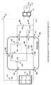
예를 들어, 도 1에 도시되는 실시예에 관련하여, 이하 서술되는 형광 램프 개조형은, 2W(5-10W 종래의 조명등 교체) 내지 10와트(40-100W 기본의 에드슨 전구 교체)까지의 범위에서 전방향으로 (360도 각도) 빛을 제공하며, 장치는 임의의 종래의 형광 전구를 쉽게 그리고 효과적으로 교체할 수 있도록 동일한 전원 소켓과 같은 크기의 《에디슨 나사》AC전원 어댑터와 같은 물리적 형상을 가질 것으로 예상한다.For example, with respect to the embodiment shown in FIG. 1, the fluorescent lamp modifying type described below may be applied to a variety of lamps ranging from 2W (5-10W conventional light replacement) to 10W (40- 100W basic Edison light bulb replacement) (360 degrees) of light in the range, and the device has the same physical shape as an " Edison screw " AC power adapter of the same size as the same power socket to easily and effectively replace any conventional fluorescent bulb .
미국 에너지 국(DOE)은 거주 지역에서 사용되는 램프 개조형의 최소 역률을0.7로 그리고 비지니스 및 산업용 조명 부분의 최소 역률을 0.9로 할 것을 권고하였다.The US Department of Energy (DOE) recommends a minimum power factor of 0.7 for lamp-type transformers used in residential areas and a minimum power factor of 0.9 for business and industrial lighting.
그러나, 한편, 저전력 LED 램프 개조형 부품의 총비용은 《텅스텐 필라멘트》의 비용보다 더 비싸고, 한편, 이 낮은 크기의 전구의 내부 공간은 고품질의 LED 드라이버 회로를 사용하기에는 너무 작기 때문에, Phillips, GE, Lights of America와 같은 대부분의 대형 제조업체들은 이미 매우 낮은 역률(0.5-0.75)을 가진 수천 개의 LED 램프 개조형을 시장에 도입하였다.However, on the other hand, the total cost of a low-power LED lamp modifying part is more expensive than the cost of a "tungsten filament", while the internal space of this low-bulb bulb is too small to use a high quality LED driver circuit, Most large manufacturers such as Lights of America have already introduced thousands of LED lamps with very low power factor (0.5-0.75) into the market.
TI, Philips, Power Integrations, Linear Technology, iWatt, ONSEMI, Fairchild와 같은 유명한 반도체 회사들은 3년 전부터 매달 간격으로 역률이 0.9이상인 새로운 LED 드라이버 회로의 방안을 광고하고 있지만, 그러나, 이러한 방안은 아직 비용이 너무 많이 들고 그리고/또는 드라이버 회로의 크기가 램프의 제한된 허용 공간에 설치하기에는 지내 큰 것으로 하여, 대형 LED 램프 개조형 제조업체들은 현재 이러한 방안들을 전혀 이용하지 않고 있다.Famous semiconductor companies such as TI, Philips, Power Integrations, Linear Technology, iWatt, ONSEMI, and Fairchild have been advertising new LED driver circuits with a power factor of 0.9 or more every month for three years. However, Larger LED lamps manufacturers are not currently using these options at all, assuming too much and / or the size of the driver circuit is large enough to fit in the limited space of the lamp.
3.3 할로겐(투광)램프 개조형3.3 Halogen (floodlight) lamp construction
예를 들어, 도 2에서 보여주는 실시예와 관련하여, 이하 서술되는 할로겐 투광 램프 개조형은 10-14 와트 전력 범위에서 작동하기 위해 보다 크기가 크고, 동일한 《에디슨 나사》 AC 전원 어댑터를 갖고 있어야 하며, 빛을 오직 한 방향(투광)으로만 약 120도의 각도로 집중하도록 되어있다.For example, with respect to the embodiment shown in FIG. 2, the halogen light tube lamp modalities described below must be larger and have the same " Edison screw " AC power adapter to operate in the 10-14 Watt power range , The light is focused only in one direction (floodlight) at an angle of about 120 degrees.
고전력의 할로겐 전구용 LED 램프 개조형은 PFC 보드를 추가하기에 충분한 내부 허용 공간을 갖고 있지만, 그러나, 현재의 할로겐 전구의 낮은 가격을 고려하여 볼 때, 대형 제조업체들은 LED 및/또는 LED 드라이버 보드의 가격이 상당히 감소하기 전에는 고품질 램프 개조형을 경쟁적인 단위당 가격으로 제공할 수 없다.LED lamps for high power halogen lamps have a sufficient internal clearance to add PFC boards, but considering the low price of current halogen bulbs, large manufacturers have found that the price of LED and / or LED driver boards Prior to the significant decline, high-quality lamps can not be offered at competitive cost per unit.
3.4 형광 램프 개조형3.4 Fluorescent Lamps
예를 들어, 도 3에서 보여주는 실시예와 관련하여, 이하 서술되는 형광 램프 개조형은 Phillips, GE와 Sylvania의 표준 전원 고정 장치에 맞추기 위해 그리고 적어도 60-80 와트 형광 램프와 같은 빛 세기에 도달하기 위해 16-24와트 전력 범위에서 작동할 수 있게 하기 위해 관 형상을 가지며, 램프의 양쪽 단부에 대칭적으로 연결된 종래의 두 접속용 소켓 AC 전원 어댑터와 같은 크기를 가져야 한다.For example, in connection with the embodiment shown in FIG. 3, the fluorescent lamp modalities described below may be used to fit standard power fixtures of Phillips, GE, and Sylvania and to reach light intensity such as at least a 60-80 Watts fluorescent lamp To be able to operate in the 16-24 watts power range, it must have the same tubular shape and the same size as the two conventional socket AC power adapters symmetrically connected to both ends of the lamp.
이 특정한 개조형에 대하여, LED 램프는 큰 장점을 갖고 있으며, 그것은 비록 형광 램프의 빛 각도는 360°이지만 전등 고정 장치는 벽에 설치되므로 품질이 좋은 미러 (반사경)가 고정 장치에 포함되어 빛을 정확한 방향으로 유도하여 돌려보내지 않는 한 조명 용량의 약 50%가 낭비되게 되기 때문이다. 하기에서 T8 개조형용 LED 패널에 관한 LED 램프 개조형의 실시예와 관련하여 서술된 바와 같이, LED의 120도 빛 각도는 이러한 종류의 개조형이 정확한 방향으로 유도된 동일한 빛 세기와 더 좋은 질(태양광)을 가지도록 하며, 크고 비싼 밝은 흰색 고정 장치 또는 반사기를 이용하지 않고도 단지 15W의 전력소모로 60W 종래의 형광 램프를 대신할 수 있게 한다.For this particular type of modification, LED lamps have a big advantage, because although the fluorescent lamp's light angle is 360 °, the fixture is installed on the wall, so a good mirror (reflector) This is because about 50% of the illumination capacity is wasted unless it is guided in the correct direction and returned. As described below with respect to the LED lamp modal embodiment of the LED panel for the T8 retrofit in the following, the 120 degree light angle of the LED indicates that this type of modality has the same light intensity and better quality Sunlight) and allows a 60W conventional fluorescent lamp to be substituted with a power consumption of only 15W without using a large and expensive bright white fixture or reflector.
이러한 특정 개조형의 추가적인 장점은 교체된 램프(크고 비싼 고정 장치, 안정기와 스타터를 포함한)의 크기와 가격이 《높은 성능 높은 가격》 LED 램프를 허용할 수 있게 하지만, 유감스럽게도, 15~30개의 부품으로 구성된 PFC회로에 요구되는 추가 비용과 추가 크기때문에 아직 시장에 존재하고 있는 대부분의 T8 형광 LED 램프 개조형들은 0.9미만(일부는 심지어 0.7미만)의 역률을 갖고 있다.An additional benefit of this particular revision type is that it allows the size and price of a replaced lamp (including large and expensive fixtures, ballasts and starters) to be "high performance, high price" LED lamps, but unfortunately, Most of the T8 fluorescent LED lamp designs that are still in the market due to the additional cost and additional size required for the PFC circuitry with components have a power factor of less than 0.9 (some even even less than 0.7).
3.5 기타 램프 개조형3.5 Other lamps
예를 들어, 하기에서 도 4에서 보여주는 실시예와 관련하여 서술한 바와 같이, 기타 LED 램프 개조형들은 매우 작은 전구들, 큰 거리 조명용 나트륨 램프 또는 매우 큰 조명 패널을 교체하는데 이용될 수 있으며, 따라서 이러한 애플리케이션에서는 LED 램프 개조형이 종래의 수백 개의 백열 전구를 이용하는 조명 패널과 유사하게 많은 부속들이 직렬 및/또는 병렬 회로에서 옆으로 상호 연결되도록 하는 구형 또는 입방체 모놀리식(monolithic) 구성을 가지도록 《콤팩트 조명 엔진》설비로 각각 설계되는 것이 바람직하다.For example, as described below with respect to the embodiment shown in FIG. 4, other LED lamp modalities can be used to replace very small light bulbs, a sodium lamp for large street lighting, or very large lighting panels, In such an application, the LED lamp modifying type may be configured to have a spherical or cubic monolithic configuration in which many parts are laterally interconnected in series and / or parallel circuits, similar to an illumination panel using hundreds of conventional incandescent bulbs. And " compact lighting engine " facilities, respectively.
이상적으로는, 《콤팩트 조명 엔진》은 LED에 직접 연결된 두 부품, 즉 LED 어레이 모듈과 실리콘 마이크로칩을 포함할 수 있다.Ideally, a " compact lighting engine " may include two components directly connected to the LED, i. E. An LED array module and a silicon microchip.
Exclara, Supertex, Seoul Semiconductor와 몇몇 다른 업체들을 비롯한 세계 산업의 일부《개척자》들은 《종래의 LED 드라이버》에서 이용되는 커패시터와 코일의 필요성을 제거하고, 《모놀리식 LED 드라이버》(완전통합) 방안이 1에 가까운 역률과 90%이상의 효율을 가지도록 하는 새로운 기술을 도입하였다.Some "pioneers" in the world industry, including Exclara, Supertex, Seoul Semiconductor and several others, have eliminated the need for capacitors and coils used in "conventional LED drivers" and have developed "monolithic LED drivers" Has introduced a new technology that has a power factor close to 1 and an efficiency over 90%.
새로운 기술은 비용은 매우 낮지만, 품질은 매우 높은 LED 램프 개조형의 《최적의 방안》의 열쇠로 될 수 있을 것이다.While the new technology is very low in cost, the quality can be key to the "best practice" of highly refined LED lamps.
따라서, 본 명세서에서는 종래의 LED 드라이버와 모놀리식 LED 드라이버를 포함한 백열등, 할로겐, 나트륨 및 형광 LED 램프 개조형을 업그레이드하기 위한 몇가지 새로운 방안들을 제공한다.Accordingly, the present disclosure provides several new approaches for upgrading incandescent, halogen, sodium and fluorescent LED lamp configurations including conventional LED drivers and monolithic LED drivers.
4.4.LEDLED 램프 개조형의 주요 부품 Main parts of lamp-shaped mold
비록 일부 램프들에서 하나의 부품에 두 개 또는 그 이상의 부분품들이 합체되어 특정한 LED 램프 개조형의 조명 조작에 필요한 2-3가지 기능을 동시에 실행할 수 있는 것으로 하여 더 적은 부품수를 포함하는 것으로 나타날 수 있지만, 본 명세서에서 제공된 모든 조명 장치들사이의 공정하고 간단한 품질 대 가격 비교를 위해, 이하에서 제공된 실시예들과 유사하게, 시장에 있는 모든LED 램프 개조형들은, 동일한 일곱가지의 주요 부품, 즉: LED, LED 패널, 급전 어댑터 시스템, 하우징, 렌즈/확산 차폐막, LED 드라이버 및 LED 드라이버의 입/출력 전기 배선 시스템을 포함하는 것으로 간주된다.Although some lamps may incorporate two or more parts into a single part, it may appear to contain fewer parts as a combination of two or more functions required to operate a particular LED lamp modular lighting However, for a fair and simple quality-to-price comparison between all of the lighting devices provided herein, similar to the embodiments provided below, all LED lamp refinements on the market have the same seven major components: : It is considered to include the input / output electrical wiring system of LED, LED panel, feed adapter system, housing, lens / diffuse shield, LED driver and LED driver.
LED 램프 개조형의 성능의 품질과 동작 수명은 각각의 특정 램프 개조형의 품질 대 가격 특징을 최적화하기 위한 각각의 부품들의 물리적 구성, 전기 특성, 신뢰도와 수명뿐만 아니라 이들 부품들의 상호 조화될 수 있는 능력에 따라 결정된다.The quality and operating life of the LED lamp modular performance is determined by the physical configuration, electrical characteristics, reliability and lifetime of each component to optimize the quality-to-price characteristics of each particular lamp model, It depends on ability.
4.14.1LEDLED 및 AndLEDLED 어레이 Array
LED는 본질상 단색 발광 다이오드 또는 비선형 반도체 장치이며 30여년 전부터 대부분 전자 설비, 스테레오, 장난감, 적외선 원격 제어 및 기타 저 전력 조명 애플리케이션의 디스플레이 패널에서 이용되는 적색(또는 적외선), 녹색, 황색 및 오렌지 색과 같은 몇 가지 색상만을 발생할 수 있는 《소형 단색 광원》으로 산업에 도입되었다.LEDs are essentially monochromatic light emitting diodes or nonlinear semiconductor devices and have been available for more than 30 years in the red (or infrared), green, yellow and orange colors used in display panels for most electronics, stereo, toy, infrared remote control and other low- As a "small monochromatic light source" that can only produce a few colors, such as.
전력 소모가 작고 (20-100mW) 비용이 낮은 것으로 하여, 당시에는, 《고효율 고역률 LED 드라이버》에 대한 수요가 제기되지 않았는데 그것은, 심지어 저전력/저비용 연산 증폭기로도 LED에 《정전압, 정전류》방식으로 전기를 공급할 수 있었으며 회로의 수명을 10-20년으로 담보할 수 있었기 때문이다.At the time, there was no demand for a "high efficiency, high power factor LED driver" because even with low power / low cost operational amplifiers, "constant voltage, constant current" And the life of the circuit could be secured by 10-20 years.
지난 10년간, 청색 LED가 드디어 개발된 직후, 이들 장치의 적용분야는 극적으로 증가하였으며, 그것은, 예를 들어, RGB형 LED 램프 개조형과 관련하여 후술한 바와 같이, 임의의 비율로, 적색, 녹색과 청색(RGB)을 결합하여, 가시 스펙트럼 (《흰색》을 포함한, 적외선으로부터 자외선에 이르는)의 임의의 다른 《특정 색상》을 쉽게 얻을 수 있고, 오늘날 소형 및 초대형 TV/모니터/광고 비디오 스크린에서 이용되고 있는 고효율 《천연색 비디오 디스플레이》에 필요한 수단을 제공할 수 있기 때문이다.Immediately after the development of the blue LEDs in the past decade, the application field of these devices has increased dramatically, which can be reduced, for example, in red, green, By combining green and blue (RGB), it is possible to easily obtain any other "specific color" of the visible spectrum (from "infrared" to ultraviolet, including "white") and today's small and extra large TV / monitor / Quot; color video display " that is being used in the < / RTI >
지난 5년동안, 청색 LED 기술로부터 개발된 《초휘도 백색 LED》기술은 CREE, LumiLED, Nichia와 기타 업체들과 같은 대형 제조 업체들에 의해 급속히 발전하여, 단위당 50mW로부터 5W이상의 전력 범위에서 동작하는 다종 다양한 LED 장치를 제공할 수 있게 하였으며, 이 장치들은 직렬 및/또는 병렬 회로(종래의 다이오드 matrix 회로와 유사한)에 쉽게 연결되며 낮은 전력(1-50W) 뿐만 아니라 고 전력(100W-1kW)의 LED 램프 개조형으로도 이용될 수 있으며, 유사한 조명 전력에 대해 백열 및 할로겐 램프에 비해 AC 전력 망으로부터 전기 에너지를 5-10 적게 흡수한다.Over the past five years, "super bright white LED" technology, developed from blue LED technology, has been rapidly developed by large manufacturers such as CREE, LumiLED, Nichia and others to operate at power ranges from 50 mW to more than 5 W per unit Which can easily be connected to a series and / or parallel circuit (similar to a conventional diode matrix circuit), and can be used in a variety of applications, including low power (1-50 W) as well as high power (100 W-1 kW) It can also be used as an LED lamp modulator, absorbing 5-10 less electrical energy from an AC power network than incandescent and halogen lamps for similar lighting power.
이 전력 범위와 특히, 항공기, 선박, 가로등 및 상업용 조명 시스템과 같은 중요한 애플리케이션에서, 낮은 전력 및 비용의 연산 증폭기는 명백하게 그 작업을 담보할 수 없으며, 따라서 1W 내지 1kW의 전력 범위에서 동작할 수 있는, 보다 복합적인 《높은 신뢰성, 높은 성능, 긴 수명을 가진 LED 램프》 드라이버 회로에 대한 수요가 긴급하게 제기되고 있다.In this power range and especially in critical applications such as aircraft, ships, street lights and commercial lighting systems, low power and cost op amps can not guarantee their operation clearly and thus can operate in the power range of 1 W to 1 kW , There is an urgent need for a more complex "high reliability, high performance, long life LED lamp" driver circuit.
LED 램프 개조형의 임의의 주어진 전력에서 적은 개수의 LED를 이용하는 장점을 제공하는 고전류(100mA 내지 5A) LED의 출현 후, 오늘날 50mW LED는 최고 20mA 의 정전압을 필요로 하며, 그 단위당 가격은 매우 낮다. 동일한 전력 범위에서, 전력이 각각 50mW인 100개의 LED의 비용은 오늘날 전력이 각각 1W인 5개의 LED보다 낮지만, 5개의 LED는 단 한개의 스트라이프에 연결될 수 있고 단 한개의 정전압 싱크 장치에 의해 전류가 안정되는 반면에, 100개의 저 전력 LED는 20개의 정전류 싱크 장치(매 스트라이프 당 5개의 LED와 같은 구성으로)를 필요로 하는 것으로 하여 대부분의 설계자들은 보다 가격이 높은 고전력의 5개의 LED를 이용하려고 한다. 남 아시아 제조 업체들은 저비용 저전력 LED를 더 많이 이용하는데, 20-30개의 스트라이프로 연결된 수백 개의 LED를 단 하나의 T8 형광 개조형 램프에서 이용하며, 각각의 스트라이프에 정전압 싱크장치 대신 저비용 안정 저항기를 이용한다. 이 방안은 오직 단위당 개조 가격을 낮추는데만 유리하며, 예를 들어, 도 24에서 보여주는 실시예와 관련하여 후술한 바와 같이, 이러한 램프가 2년 이상 동작할 수 있는 가능성은 매우 낮다.After the advent of high current (100mA to 5A) LEDs that offer the advantage of using a small number of LEDs at any given power of LED lamps, today 50mW LEDs require a constant voltage up to 20mA and the price per unit is very low . In the same power range, the cost of 100 LEDs each with a power of 50 mW is lower than the five LEDs with today's power of 1 W each, but five LEDs can be connected to only one stripe and only one current sink While 100 low-power LEDs require 20 constant-current sink devices (with the same configuration as five LEDs per strip), most designers use five LEDs with higher power and higher prices I will try. South Asian manufacturers use more low-cost, low-power LEDs, using hundreds of LEDs connected in 20-30 stripes on a single T8 fluorescent lamp, using a low-cost stable resistor instead of a constant-voltage sink in each stripe . This option is advantageous only for lowering the unit cost per unit, and the possibility that such a lamp can operate for more than two years is very low, for example, as described below in connection with the embodiment shown in FIG.
예를 들어, 도 4와 20에서 보여주는 실시예와 관련하여 후술한 바와 같이, 많은 LED 제조업체들은 오늘날 《산화 알루미늄》 기판에 인쇄 회로를 침적시킬 수 있는 매우 생산적이며 비용 효과적인 기술을 이용하여 2, 6, 15개 이상의 LED가 얇은 알루미늄 판에 집적되어 장착된 다음 직렬 및/또는 병렬로 상호 연결되는 일명 《LED 어레이》, 《6V LED》, 《20V LED》 또는 《50V LED》를 제공하였으며, 한 개 이상의 LED를 이용한 LED 램프 개조형의 제조 공정에서 나서는 열 전달 및 전기 절연 문제를 동시에 해결하였다.For example, as described below in connection with the embodiments shown in FIGS. 4 and 20, many LED manufacturers use the highly productive and cost-effective techniques that can deposit printed circuit boards on today's "aluminum oxide" , More than 15 LEDs were integrated in a thin aluminum plate and then provided a so-called "LED array", "6V LED", "20V LED" or "50V LED" interconnected in series and / In the manufacturing process of LED lamps using the above LEDs, heat transfer and electrical insulation problems were simultaneously solved.
종래의 램프에 대한 LED의 주요 장점은: 보다 콤팩트하고, 크기와 중량이 작으며, 효율과 효력이 높고, 열 손실이 적으며, 기계적인 충격과 진동에 대한 견딜성이 높고, 빛 스펙트럼이 정밀하게 제어되며, 자외선 또는 x-선 방사선이 없고 폐기/재생 문제가 제기되지 않는다는 것이다.The main advantages of LEDs for conventional lamps are: they are more compact, smaller in size and weight, higher in efficiency and efficacy, less in heat loss, more tolerant to mechanical shocks and vibrations, And there is no ultraviolet or x-ray radiation and no disposal / recycling problem is raised.
LED의 동작 과정에서 제기되는 기본 문제점은 비선형 측면이며, 이것은 일반적으로 LED가 단자를 통과하는 전압이 0V로부터 약 2.8V로 증가할 때 전류를 거의 전혀 흡수하지 못하고, 그 후 전압이 2.8V와 3.3V사이로 공급될 때 점점 더 많은 전류를 빠른 속도로 흡수하기 시작하며, 심지어 전압을 0.1-0.2 볼트만 증가시켜(그리고 LED의 전류를 일정한 방법으로 제한하지 않으면서), LED의 전류가 권장 한계 이상으로 증가되는 경우, LED가 결국 돌이킬 수 없는 손상을 받을(또는 간단히 말해서《폭파》될) 위험이 있는 것과 관련된다.The basic problem posed in the operation of LEDs is the non-linear side, which generally causes the LEDs to absorb almost no current when the voltage across the terminals increases from 0 V to about 2.8 V, V, it starts absorbing more and more current at a faster rate and even increases the voltage by 0.1-0.2 volts (and without limiting the LED current in a certain way) , There is a risk that the LED will eventually suffer irreversible damage (or simply " blow up ").
다른 문제점들은 LED가 상대적으로 정교한 고가의 역률 보정 회로를 요구하는 정류된 AC전류를 필요로 하며, LED의 전류 량은 주위 온도의 변화와 함께 상당한 정도로 변화되며, 병렬 스트라이프로 연결된 경우 LED는 각각의 유닛의 스트라이프 당 전류를 안정시키기 위한 안정 저항기 또는 정전류 싱크가 있어야 하며, 특히 조광기를 사용할 경우 LED 스트라이프를 통과하는 전압이 2.8V-3.3V의 전형적인 한계값보다 불과 조금만 낮아져도 완전히 조명이 꺼지면서 신경을 자극하는 《깜박임》효과를 발생시킨다는 사실이다.Other problems require a rectified AC current that requires a relatively sophisticated and expensive power factor correction circuitry, the amount of current in the LED varies considerably with ambient temperature changes, and when connected in parallel stripes, There should be a stabilizing resistor or constant current sink to stabilize the current per unit of stripe, especially if the dimmer is used, the voltage across the LED stripe will be slightly lower than the typical limit of 2.8V-3.3V, It is the fact that it generates a "flicker" effect.
결론적으로, LED는 점차적으로 현존하는 모든 종래의 램프를 교체하게 될 미래의 이상적인 광원으로 될 수 있는 강한 잠재력을 갖고 있지만, 일부 문제점들로 하여, 매우 콤팩트하며 효율적인 이 장치는 다양한 실시예들의 배합 및 변경들에서 후술되는 6개의 기타 부품들 매개와의 또한 모두와의 《완전한 조화》를 떠나서는 효율적이며 안전한 램프 개조형으로 예상대로 동작할 수 없게 된다.In conclusion, LEDs have a strong potential to become an ideal light source for the future, which will gradually replace all existing conventional lamps, but due to some problems, this device is very compact and efficient, Except for the "perfect harmony" with all six of the other parts of the vehicle described later in the modifications, the efficient and safe lamp configuration will not work as expected.
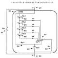
4.24.2LEDLED 패널 panel
LED 패널은, 본질상, 특정한 LED 램프 개조형에 포함된 매개의 특정한 LED 패널의 램프의 물리적 구성, 허용 내부 공간, 빛 방향, 조광 능력 및 균일한 빛 분포에 대하여 최적의 구현 또는 최대 휘도를 제공하는 임의의 직렬 또는 병렬 회로 결합으로 연결된 한 개 이상의 LED에 대한 기계적인 지원 장치이다.The LED panel, by its nature, provides the optimum implementation or maximum brightness for the physical configuration of the lamp of the particular LED panel of the medium included in the particular LED lamp modifying mold, the permissible inner space, the light direction, dimming capability and uniform light distribution Which is a mechanical support device for one or more LEDs connected in any serial or parallel circuit combination.
LED 패널의 구성과 LED 사이의 기계적인 연결은 반사경을 이용하거나 이용하지 않으면서 최대의 휘도를 제공할 수 있는 방식으로, 또한, 최대 공급 전압이 내려가서 조광기가 모든 LED 스트라이프를 하나 하나씩 《off》로 전환하여 최대 공급 전압을 감소시키는 경우에도, 빛이 LED 패널 표면 전체에 대칭적으로 분포될 수 있도록 설계되어야 한다.The mechanical connection between the LED panel's construction and the LEDs can be achieved by providing maximum brightness without using or using reflectors, and also by reducing the maximum supply voltage so that the dimmer can "turn off" all LED stripes one by one, So that the light can be distributed symmetrically over the surface of the LED panel.
다음의 네 가지 주요 LED 패널 구성이 현재 이용되고 있거나 이용될 수 있을 것이다:The following four major LED panel configurations are currently available or may be used:
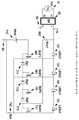
a) 도 5 및 도 6에서 실례로 도시되는 실시예와 관련하여 후술된 바와 같이 급전 피크(peak)의 진폭이 감소하는 경우, 전방향성 및 대칭 분포된 빛을 보장해야 하는 백열 LED 램프 개조형을 위한 3차원 LED 패널.a) An incandescent LED lamp rebar that must ensure omnidirectional and symmetrically distributed light when the amplitude of the feed peak decreases, as described below with respect to the exemplary embodiment shown in Figs. 5 and 6 Three-dimensional LED panel for.
b) 할로겐(투광) LED 램프 개조형을 위한 평판 디스크 LED 패널: 도 6에서 실례로 보여주는 실시예와 관련하여 후술된 바와 같이 피크 입력 전압의 진폭이 감소하는 경우 국부 조명과 대칭 분포된 빛을 제공하는 도 2에서 실례로 도시된 실시예와 관련하여 후술된 할로겐(투광) LED 램프 개조형을 위한 평면 디스크 LED 패널.b) Flat panel discs for halogen (flood) LED lamps: Provides light that is symmetrically distributed with the local illumination when the amplitude of the peak input voltage decreases, as described below in connection with the illustrative embodiment of FIG. A flat panel LED panel for a halogen (floodlight) LED lamp modality as described below in connection with an exemplary embodiment shown in Fig. 2.
c) 도 5에서 실례로 도시되는 실시예와 관련하여 후술된 바와 같이 급전 피크 전압의 진폭이 감소하는 경우, 수 피트 길이의 투명관과 빛이 대칭 분포되어 있어야 할 곳에 균일한 빛을 제공하는 도 3에서 실례로 도시되는 실시예와 관련하여 후술된 형광 LED 램프 개조형을 위한 평면 직사각형 LED 패널.c) When the amplitude of the feed peak voltage decreases as described below with respect to the embodiment shown in Fig. 5, a transparent tube of several feet long and a figure providing uniform light where the light should be symmetrically distributed A flat rectangular LED panel for a fluorescent LED lamp refinish type described below in connection with an embodiment illustrated by way of example in FIG.
d) 도 7에서 실례로 도시되는 실시예와 관련하여 후술된 바와 같이 급전 전압의 진폭이 감소하는 경우 균일하고 대칭 분포된 빛을 제공하는 도 4에서 실례로 도시되는 실시예와 관련하여 후술된 모놀리식 광 엔진 LED 램프 개조형 평면 소형LED 어레이.4, which provides uniform and symmetrically distributed light when the amplitude of the feed voltage is reduced, as described below in connection with the exemplary embodiment shown in Fig. 7; Amorphous light engine LED lamp Modified flat small LED array.
4.3 급전 어댑터4.3 Feeding adapter
임의의 램프 개조형에서, 급전 어댑터는 하나의 부품이며, 최종 사용자가, 새로운 램프를 위험한 고압 전력망의 표준 단자에 연결하기 위해 허가받은 전기 기사를 고용하지 않고 그리고/또는 《즉석 수리》하는 모험을 하지 않고도, 교체 날짜까지 사용한 낡은 종래의 램프를 간단히 및 작동적으로 교체할 수 있게 한다.In any lamp-modal version, the feed adapter is a component, and the end user is not entitled to hire an authorized electrician to connect a new lamp to the standard terminals of the hazardous high voltage power grid and / or to " Without having to replace the old conventional lamp used up to the replacement date.
따라서 대부분의 LED 램프 개조형에는 교체 대상인 표준 전력과 크기의 백열, 할로겐, 나트륨 그리고 형광 램프를 위하여 상기 서술된 바와 같은 급전 어댑터가 장착된다.Thus, most LED lamps are equipped with a feed adapter as described above for the standard power and size of incandescent, halogen, sodium and fluorescent lamps to be replaced.
4.44.4하우징housing
LED 램프 개조형의 하우징은, LED가 빛을 생성하기 위해 진공 또는 불활성 기체를 필요로 하지 않기 때문에 합성 수지나 알루미늄보다 무겁고 깨지기 쉽고 비싼 유리로 하우징을 만들 필요가 없으므로 종래의 램프 하우징에 비해, 중요한 경제적인 장점을 갖고있다.The LED-lamp-shaped housing is more important than conventional lamp housings because LEDs do not require vacuum or inert gas to generate light, so they are heavier than synthetic resins or aluminum, It has economic advantages.
하우징은 개조형 램프의 기타 모든 부품들에 대한 기계적 지원 및 환경상의 보호(비, 습기 또는 먼지에 대한)를 제공하며, 또한 렌즈/확산 차폐막을 대신하는 투명한 합성 수지로 만든 구의 형상을 가지거나 또는 알루미늄으로 제조할 수 있으며 동작 온도를 감소시키고 높은 효율을 유지하도록 하기 위한 LED 패널 또한 LED 열 싱크로 이용할 수 있다.The housing provides mechanical support and environmental protection (against rain, moisture or dust) for all other components of the lamp and also has the shape of a sphere made of clear synthetic resin to replace the lens / diffusion shield, or LED panels can also be used as LED heat sinks, which can be fabricated from aluminum and reduce operating temperatures and maintain high efficiency.
하우징을 알루미늄으로 또는 임의의 다른 금속으로 제조하는 경우, 최종 사용자를 전기 충격으로부터 보호하기 위해, 예를 들어, 모놀리식 드라이버와 같은 비절연 드라이버의 실시예와 관련하여 후술되는 바와 같이, AC 전력망에 직접 연결된 하우징과 임의의 전기 부품들(LED, LED 패널, LED 드라이버, 급전 어댑터, 배선 급전 회로) 사이에 2kV-4kV의 절연체가 들어가도록 하는데 신중한 주의를 돌려야 한다.When the housing is made of aluminum or any other metal, as described below in connection with embodiments of non-insulating drivers such as, for example, a monolithic driver, an AC power grid Care must be taken to ensure that a 2kV-4kV insulator is inserted between the housing and any electrical components (LED, LED panel, LED driver, feed adapter, wiring feed circuit) directly connected to the power supply.
4.5 렌즈/확산4.5 Lens / Diffusion차폐막Shielding film
지금의 LED 램프 개조형의 렌즈/확산 차폐막은 상이한 이유로 특정한 램프 유형을 매우 선호하는 최종 사용자들에게 적어도 같은 빛 강도와 품질, 스펙트럼을 제공하기 위해 교체 대상인 종래의 램프의 정확한 외형을 최대한 비슷하게 따르는 상이한 크기와 형상, 투명도(투명, 반투명, 유백색, 색 필터, 확대경 줄무늬 등)를 갖고있다.The present LED lamp modifying lens / diffuse shielding film is a different type of lens / diffuse shielding film that follows the exact contours of the conventional lamps to be replaced as closely as possible to provide at least the same light intensity, quality, and spectrum to end users who prefer a particular lamp type for different reasons It has size and shape, transparency (transparent, translucent, milky white, color filter, magnifying glass stripe, etc.).
시장에 존재하는 일부LED들은 플라스틱 패키지에 합체된 작은 확대 렌즈가 함께 제공되며, 이것은 LED의 휘도를 증가시키지만 광 원추(light cone)의 각도를 약 90°까지 감소시킨다.Some LEDs on the market come with a small magnifying lens incorporated in a plastic package that increases the brightness of the LED but reduces the angle of the light cone by about 90 °.
외부 애플리케이션에서, 렌즈/확산 차폐막 장치는 LED 램프의 회로를 손상시킬 수 있는 비, 먼지 또는 임의의 기타 역작용 요인들에 대하여 램프의 높은 신뢰성을 보장하기 위해 LED 램프 개조형의 하우징에 밀봉(방수) 결합되어야 한다.In an external application, the lens / diffusion shielding device is sealed (watertight) to the LED lamp modular housing to ensure high reliability of the lamp against rain, dust or any other adverse factors that could damage the circuit of the LED lamp. Should be combined.
4.4.6 입6 mouth/출력 전기 배선 시스템/ Output electrical wiring system
LED 드라이버의 입/출력 전기 배선 시스템은 다음의 3가지 주요 회로:The input / output electrical wiring system of the LED driver has the following three main circuits:
a) 드라이버 급전회로, 차 배터리와 같은 DC전원, 120V-240V전력망과 같은 고압 AC 전원, 또는 50-60Hz 전원 변압기에 연결되는 두 개 이상의 와이어로 구성된 드라이버 급전회로,a) a driver power supply circuit consisting of a driver power supply circuit, a DC power source such as a car battery, a high voltage AC power source such as a 120V-240V power network, or two or more wires connected to a 50-60Hz power transformer,
b) LED 드라이버와 LED 패널 회로의 구성에 따라는 두개 이상의 와이어를 포함할 수 있는 LED급전 회로,b) LED power supply circuit, which may include two or more wires depending on the configuration of LED driver and LED panel circuit,
c) 입/출력 자료를 교환할 수 있는 감지기와 마이크로 정류기 시스템을 포함하는 LED 드라이버 회로와 그리고 LED 램프 개조형을 외부 컴퓨터 시스템과 인터넷에 직접 연결하는 《입/출력 자료 연결기》사이에 결합된 2개 또는 그 이상의 와이어를 포함하는 원격 피드백 배선 회로c) LED driver circuitry including a detector and micro-rectifier system capable of exchanging input / output data, and an LED driver circuit coupled between an "input / output data connector" that directly connects the LED lamp architecture to an external computer system and the Internet A remote feedback wiring circuit including one or more wires
로 구성된다..
현재, 최종 사용자가 인터넷을 통하여, 해외 출장중에도, 아파트의 조명을 on/off로 하거나 어둡게 할 수도 있는 《스마트 원격 제어 회로》가 이미 출현하였다.Currently, a "smart remote control circuit" has appeared, which allows end users to turn on / off or dim the lighting of an apartment, even on an international trip, via the Internet.
4.74.7LEDLED 드라이버 driver
현재 세계 시장에는 수백 개의 서로 다른 LED 드라이버 회로 구성들이 출현하였으며, 각기 서로 다른 회로 배치를 따르며 저비용, 작은 크기, 적은 부품수, 고효율, 고역률, 적은 고조파(소음), 오프라인 (90-240Vac 급전 범위) 기능, 넓은 범위의 조광 기능과 같은 상이한 장점들을 제공하지만 각각 일부 제한점들 및 문제점들도 갖고 있다.There are now hundreds of different LED driver circuit configurations on the world market, each with a different circuit layout and with low cost, small size, small parts count, high efficiency, high power factor, low harmonic (noise), offline (90-240Vac feed range ) Function, and a wide range of dimming functions, but each also has some limitations and problems.
매우 일반적으로, 이러한 장치들은 두 가지 주요 그룹, 즉: a) 안정기 LED 드라이버, b) 스위치 방식(SMPS) 전력 공급 LED 드라이버 및 c) 모놀리식 LED 드라이버로 나눠질 수 있으며, 이들 모두는, 브리지 정류기가 AC/DC 전환을 실행하는 경우 모두 DC/DC 또는 AC/DC LED 드라이버 회로로 동작할 수 있다.Very generally, these devices can be divided into two main groups: a) ballast LED driver, b) switched-mode (SMPS) powered LED driver, and c) monolithic LED driver, When the rectifier performs an AC / DC conversion, it can operate as both a DC / DC or AC / DC LED driver circuit.
안정 LED 드라이버는 제일 간단하고 비용 효과적인 드라이버이며, 한 개 이상의 LED에 직렬로 연결된 저항기 또는 간단한 정전류 싱크(CCS) 회로로 구성되어 있다.The stable LED driver is the simplest and most cost-effective driver, consisting of a resistor or simple constant current sink (CCS) circuit connected in series to one or more LEDs.
SMPS LED 드라이버는 현재 LED 조명 산업에서 가장 많이 이용되는 장치이며, 종래의(30년이상 된) 펄스 폭 변조(PWM) 변환기 제어 방법을 따르며, 코일과 커패시터의 전기 에너지의 저장 기능에 기초하고 있으며, 현재 세계 시장에서 TI, Phillips, Maxim, ST 마이크로, Toshiba, Fairchild, ONSEMI, Power Integrations, Semtech, Linear Technology 및 기타 다른 모든 주요 전력 관리 회사들에 의해 판매 촉진되고 있다.The SMPS LED driver is currently the most widely used device in the LED lighting industry and is based on the traditional (over 30 years) pulse width modulation (PWM) converter control method, the storage function of the coil and capacitor electrical energy, It is currently being marketed by TI, Phillips, Maxim, ST Micro, Toshiba, Fairchild, ONSEMI, Power Integrations, Semtech, Linear Technology and all other major power management companies in the global market.
모놀리식 LED 드라이버는 코일과 커패시터가 필요 없으며 매우 콤팩트하고 비용 효과적이며 완전 일체화된 드라이버 회로 방안으로 되는 독특한 제어 법을 제공하고, 이 방법은 Exclara, Seoul Semiconductor, Samsung, Supertex와 몇몇 다른 업체들을 비롯한 세계 산업의 일부《개척자》들에 의해 최근 시장에서 도입되었다.The monolithic LED driver provides a unique control method that eliminates the need for coils and capacitors and is a very compact, cost-effective, and fully integrated driver circuit approach that can be used in a variety of applications including Excarade, Seoul Semiconductor, Samsung, Supertex, It has recently been introduced in the market by some "pioneers" of the global industry.
상기 서술된 3가지 제어 방법들은 여러가지 서로 다른 회로 토폴로지 애플리케이션을 허용하지만, 각자에 대해 단점들을 갖고있고 SMPS LED 드라이버와 모놀리식 LED 드라이버는 모두 본 명세서의 중요한 대상이므로 유명한 전력 관리 회사들에서 추진되고 있는 몇 가지 LED 드라이버 회로 방안에 대한 구체적인 설명이 하기에서 서술되게 된다.While the three control methods described above allow for different circuit topology applications, they have disadvantages to each other, and since SMPS LED drivers and monolithic LED drivers are both an important subject matter in this specification, they are propelled by famous power management companies A detailed description of some LED driver circuit schemes will be described below.
5. 간단한 안정5. Simple stabilityLEDLED 드라이버 회로 Driver circuit
5.1 저항 안정5.1 Resistance StabilityLEDLED 드라이버 driver
저전력 범위 및 안정 전압(정전압) DC/DC 애플리케이션에서, 실내 온도(23°-25°C)에서 동작하는 LED 드라이버 회로는 LED 와 직렬로 연결된 단 《한 개의 저항기》(가격이 $0.01 미만), 또는 한 개의 LED 스트라이프로 구성되어 있으며, 장치별로 상이한 LED 전류/전압 사양에 대하여(LED사양 허용 범위), 그리고 주위 온도 및/또는 급전 전압 리플의 작은 변화에 대하여 《안전 여유》를 보장하기 위해 LED의 전류를, 전형적으로, LED의 최대 등급 사양의 80%이하인 안전 양으로 제한하기 위한 《안정기 회로》로서 매우 간단하고 비용 효과적일 것이다.Low Power Range and Stable Voltage For DC / DC applications, LED driver circuits operating at room temperature (23 ° -25 ° C) require only one "resistor" (less than $ 0.01) connected in series with the LED, or It consists of a single LED stripe and is designed to meet the different LED current / voltage specifications for each device (LED specification tolerance) and to ensure a "safety margin" for small changes in ambient temperature and / or supply voltage ripple. As a " ballast circuit " for limiting the current to a safe amount, typically not more than 80% of the maximum rating specification of the LED.
간단한 예로서, 급전 전압이 12V DC인 자동차 배터리로부터 얻어지는 애플리케이션에서, 각각의 LED 당 필요한 전압은 3.2V이며 최대 평균 전류 Imax는 20mA (Imax의 80% 인 16mA Imax)이며, 가장 《간단한 드라이버》는 3.2V x 3 = 9.6V를 필요로 하는 세 개 LED의 《스트라이프》(직렬로 연결된 장치의 열)와 직렬 연결된 저항기이며 여기서 저항 값은 12V - 9.6V = 2.4V / 0.016A = 150 Ohms이며, 시스템 효율은 Eff = 9.6/12 = 80%이다.As a simple example, for applications derived from automotive batteries with a supply voltage of 12V DC, the required voltage per LED is 3.2V and the maximum average current Imax is 20mA (16mA Imax, 80% of Imax) Resistors in series with three "stripes" of LEDs (rows of devices connected in series) requiring 3.2V x 3 = 9.6V where the resistance value is 12V - 9.6V = 2.4V / 0.016A = 150 Ohms, The system efficiency is Eff = 9.6 / 12 = 80%.
《더 많은 빛》을 얻기 위해, 약 150 Ohms의 안전 저항기를 가진 다수의 3 LED 스트라이프들은 병렬로 연결될 수 있으며, 바람직하고 안정적인 환경 조건에서, 이 특정 시스템의 실질적으로 낮은 효율을 무시한다면, 저항기는 자동차 산업에서 이용되고 있는 종래의 백열 또는 할로겐 전구를 교체하기 위해 지정된 LED 램프 개조형에 포함되는 가장 간단하고 비용이 낮은 드라이버로 될 것이다.To obtain " more light ", a plurality of 3 LED stripes with a safety resistor of about 150 Ohms may be connected in parallel and, under desirable and stable environmental conditions, ignoring the substantially lower efficiency of this particular system, It will be the simplest and lowest cost driver included in a designated LED lamp rebuild to replace conventional incandescent or halogen bulbs used in the automotive industry.
그러나, 실제 상황에서, 상기 서술된 간단한 방안은 급전 전압 (자동차 배터리 전압은 9V로부터 15V로 변동될 수 있음) 또는 주위 온도(여름 대 겨울 계절)의 큰 변화에 대처하여 LED를 보호하지 않으며 또한 추가적으로 안전 저항기에서는 상당한 비율의 급전 전기 에너지가 열 손실되어 LED 램프 개조형의 효율을 80%로 또는 그 아래로 감소시키는 많은 단점들을 갖고 있다.However, in the actual situation, the above-described simple measures do not protect the LED against large changes in the supply voltage (the car battery voltage can vary from 9V to 15V) or ambient temperature (summer-winter season) Resistors have a number of disadvantages that reduce the efficiency of LED lamps to 80% or below due to the heat loss of a significant percentage of the feed electrical energy.
따라서, 이러한 단점들을 극복하기 위해, 전기 에너지를 빛으로 전환하는데서 최대 효율에 도달할 수 있는 방식으로, LED 전류와 전압을 급전 전압 및/또는 주위온도의 큰 변화 속에서도, 사전 설정된 정확한 한계내에서 유지할 수 있는 보다 복합적인 LED 드라이버 회로에 대한 수요가 제기되고 있다.To overcome these drawbacks, therefore, it is desirable to maintain the LED current and voltage within predetermined precise limits, even during large changes in the supply voltage and / or the ambient temperature, in such a way as to achieve maximum efficiency in converting electrical energy into light There is a demand for a more complex LED driver circuit that can be made.
5.2 정전압5.2 Constant Voltage싱크SinkLEDLED 드라이버 driver
정전류 싱크 (《CCS》) 드라이버는 주위온도가 크게 변화되어도 LED 스트라이프를 통하여 안전한 전류를 보장할 수 있지만, 그러나, 급전 전압이 LED 스트라이프의 한계 전압보다 훨씬 높게 증가하는 경우, 전압에서의 차이는 CCS 장치의 열손실을 증가시키며 그에 따라 드라이버의 효율을 감소시킬 것이다. 한편, 시스템 급전 전압이 LED 스트라이프의 한계 전압보다 내려가는 경우, 짧은 시간동안(리플)이라도, 전체 LED 스트라이프는, 그 시간 동안, 빛을 차단하고 신경을 자극하는 깜박임 (스트로보스코프) 효과를 발생시키게 된다.A constant current sink (" CCS ") driver can guarantee a safe current through LED striping even with large ambient temperature changes, but if the supply voltage is much higher than the LED stripe limit voltage, Will increase the heat loss of the device and thereby reduce the efficiency of the driver. On the other hand, if the system feed voltage drops below the limit voltage of the LED stripe, even for a short time (ripple), the entire LED stripe will produce a flicker (stroboscopic) effect that blocks the light and stimulates the nerve during that time .
결론적으로, CCS 장치는 급전 전압이 합리적으로 일정(작은 리플)하고 LED 스트라이프의 한계 전압에 가까운 DC 회로에서만 유용하며 그 사용이 권고되고 있다.In conclusion, CCS devices are only useful in DC circuits where the supply voltage is reasonably constant (small ripple) and close to the threshold voltage of the LED stripe, and its use is recommended.
그럼에도 불구하고, 이미 시장에는 AC 회로에서도 (브리지 정류기를 통하여) 이용되는 매우 낮은 가격의 CCS LED 드라이버가 판매되고 있으며, 이들의 낮은 효율과 역률, A.THD 파라미터들은 이 종류의 드라이버들이, 세계적인 시장에서, 바람직한 《저비용 고성능》 LED 드라이버로 되게 하는데 커다란 장벽을 조성하고 있다.Nevertheless, there are already very low cost CCS LED drivers on the market that are used in AC circuits (via bridge rectifiers), their low efficiency and power factor, A. THD parameters, Which is a desirable " low cost high performance " LED driver.
6. 스위치 형 전원 공급(6. Switched power supply (SMPSSMPS))LEDLED 드라이버 driver
SMPS LED 드라이버 회로는 인덕터 및 커패시터와 같은 전기 에너지를 저장하고 변환할 수 있는 리액티브 부품뿐만 아니라 집적 회로, 트랜지스터, 다이오드 및 저항기를 포함하는 종래의 펄스 폭 변조(PWM) 부스트, 벅, 벅-부스트 또는 플라이백 변압기 변환기 회로 토폴로지를 따른다.The SMPS LED driver circuit includes conventional pulse width modulated (PWM) boost, buck, buck-boost (not shown) including integrated circuits, transistors, diodes and resistors as well as reactive components capable of storing and converting electrical energy such as inductors and capacitors Or flyback transformer converter circuit topology.
SMPS 드라이버의 기본 단점은 드라이버가 전기 에너지를 변환 및 저장하기 위한 진동 코일과 전해 커패시터와, SMPS 변환기가 생성하는 고주파수 소음이 전력 망에 침습하는 것을 차단하는 EMI (저주파) 필터를 위한 필터링 코일과 고압 커패시터와 같은 부피가 크고 불안정한 리액티브 부품들에 의존한다는 것이다.The main disadvantages of the SMPS driver are the vibration coil and electrolytic capacitor for the driver to convert and store electrical energy, the filtering coil for the EMI (low frequency) filter that blocks the high frequency noise generated by the SMPS converter from invading the power grid, It relies on bulky and unstable reactive components such as capacitors.
LED 램프 개조형의 내부에서 예상되는 상대적으로 높은 온도에서, 전해 커패시터의 수명은 상대적으로 짧으며(약 2년) 또한 주위 온도와 습도 요인으로 하여 고주파수 코일 또는 변환기(플라이백)의 절연 및/또는 자극 철심 특성이 극적으로 변화되어 전체 LED 램프 개조형 장치의 수명은 2-3년으로 제한될 수 있다.At relatively high temperatures expected within the interior of the LED lamps, the life of the electrolytic capacitors is relatively short (about two years), and insulation of high frequency coils or converters (flybacks) with ambient temperature and humidity factors and / The characteristics of the irons cores are dramatically changed, and the lifetime of the entire LED lamp modifying device may be limited to 2-3 years.
6.16.1DCDC//DCDCSMPSSMPSLEDLED 드라이버 driver
DC/DC SMPS LED 드라이버는, 고주파 출력 정전압 펄스의 형태로 주기적으로 전기 에너지를 부하(LED)에 저장 및 전달할 수 있는 제어 회로(반도체)와 진동 유도자(코일)를 포함하고, 그를 통해 깜박임이 없이 LED 조명을 유지하게 위해 전기 에너지를 저장하는 커패시터가 있는, PWM 변환기를 이용하여, 종래의 방식으로 모든 안정 LED 드라이버의 단점을 극복할 수 있다. 현대적인 PWM 제어 집적 회로(IC)에서는 시스템 급전 전압이 낮아지거나, 또는 LED 스트라이프의 한계 전압보다 10배 이상 높은 경우에도 LED 스트라이프를 통과하는 전압은 정전압 상태를 유지하며, 깜박임을 방지하고 시스템의 효율을 최대화하기 위해 LED 스트라이프의 한계 전압보다 약간 높은 방식으로 출력 전압을 조절할 수 있다.The DC / DC SMPS LED driver includes a control circuit (semiconductor) and a vibration inductor (coil) capable of periodically storing and delivering electrical energy to a load (LED) in the form of a high frequency output constant voltage pulse, Using PWM converters, which have capacitors that store electrical energy to maintain LED illumination, the disadvantages of all stable LED drivers can be overcome in a conventional manner. In modern PWM control integrated circuits (ICs), the voltage across the LED stripes remains constant, even when the system supply voltage is low, or even 10 times higher than the limit voltage of the LED stripes, to prevent flicker, The output voltage can be adjusted in a manner slightly higher than the threshold voltage of the LED stripe to maximize the output voltage.
6.2 정전압 정전류6.2 Constant Voltage Constant CurrentLEDLED 드라이버 driver
정전압 정전류(CVCC) LED 드라이버는 LED 전압과 전류 파라미터의 안정성을 가장 높은 수준에서 보장하며, 또한 LED 램프 개조형의 수명을 각각의 부품들, 특히 불안전한 고압 전해 커패시터가 허용하는 최대 기간으로 연장하기 위해 PWM 변환기와 CCS 장치를 모두 이용한다.Constant-voltage constant-current (CVCC) LED drivers guarantee the highest level of stability of LED voltage and current parameters and also extend the lifetime of the LED lamps to the maximum duration allowed by each component, especially unsecure high-voltage electrolytic capacitors Both PWM converters and CCS devices are used.
신뢰성이 매우 높은 CVCC LED 드라이버 방안을 달성하기 위해, 연산 증폭기(OPAM)의 피드백을 받는 MOSFET 완충 트랜지스터를 포함한 종래의 CCS회로는 장기간의 수명을 담보하기 위해 각각의 LED 스트라이프와 직렬로 LED 램프 개조형에 삽입되는 것이 바람직하다. 두 가지 좋은 예로서, Maxim에서 제공한 MAX16834 LED 드라이버 칩과 Linear Technology에서 제공한 LT3756 LED 드라이버 칩은, 모두 내부 OPAM에 의해 제어되는 추가적인 외부 MOSFET 버퍼를 CCS로 이용하여, 현존 기술의 CVCC회로의 구현을 제공할 수 있지만, 이 보호는 오직 한 개의 LED 스트라이프에만 해당된다. 3개 이상의 스트라이프에는 이러한 매우 안전한 OPAM-MOSFET-CCS회로를 이용하는데 너무 비용이 많이 들며 따라서 설계자들은 더 많은 스트라이프로 연결된 더 저렴한 LED들보다는 전력이 높은 단 한 개의 스트라이프와 보다 비싼 LED들을 이용하는 것을 선호한다. 따라서, 여러가지 실시예에서, 본 명세서는, 예를 들어, 도 8과 9와의 관련속에서 후술된 바와 같이 CVCC LED 드라이버를 제공한다.To achieve a highly reliable CVCC LED driver scheme, conventional CCS circuits, including MOSFET buffering transistors that receive feedback from op amps (OPAMs), are designed with LED lamps in series with each LED stripe to ensure long- As shown in Fig. As two good examples, the MAX16834 LED driver chip from Maxim and the LT3756 LED driver chip from Linear Technology both use an external external MOSFET buffer, controlled by internal OPAM, as the CCS to implement the existing CVCC circuitry But this protection is only for one LED stripe. More than three stripes are too costly to use this very secure OPAM-MOSFET-CCS circuitry, so designers prefer to use only one stripe and more expensive LEDs with higher power than the more inexpensive LEDs connected by more stripes do. Thus, in various embodiments, the present disclosure provides a CVCC LED driver, for example, as described below in the context of Figures 8 and 9.
DC/DC SMPS LED 램프 개조형의 최대 효율은 각각의 스트라이프당 LED의 개수와 LED 드라이버에 이용되는 PWM 회로 토폴로지에 따라 결정된다. 한 개의 스트라이프에 직렬로 연결된 LED가 많을수록 전압치 한계값이 높아지며, 그에 따라, 동일한 전력 범위에서 전체 회로의 전류가 낮아질 것이다. 낮은 전류는 낮은 열을 의미하며 이것은 적은 소모와 높은 효율을 의미한다. 그러나, 상기 서술한 네 개의 종래의 PWM회로 토폴로지는 다음의 자기의 고유한 장점과 단점들을 갖고 있다:The maximum efficiency of a DC / DC SMPS LED lamp rebuild depends on the number of LEDs per stripe and the PWM circuit topology used for the LED driver. The more LEDs connected in series to one stripe, the higher the voltage value threshold, and thus the current in the entire circuit will be lower in the same power range. Low current means low heat, which means low consumption and high efficiency. However, the four conventional PWM circuit topologies described above have the following unique advantages and disadvantages:
6.36.3부스트Boost토폴로지Topology((BoostBoostTopologyTopology))
부스트 회로 토폴로지는 제일 단순하고(적은 부품수), 가장 효율적이며(전형적으로, Eff = 90-95%), 비용이 낮은 PFC 또는 PWM LED 드라이버 실시 방식을 허용하며, 두 가지 주요 단점을 갖고있다:The boost circuit topology allows for the simplest (fewer parts count), the most efficient (typically, Eff = 90-95%), low cost PFC or PWM LED driver implementation approach and has two major drawbacks:
a) 입력 및 출력 회로사이의 절연을 제공하지 않고,a) does not provide isolation between the input and output circuits,
b) 출력 전압이 항상 최대 입력 전압보다 높다.b) The output voltage is always higher than the maximum input voltage.
상기 서술한 바와 같이 10-15V가 공급되는 자동차 배터리 LED 램프 개조형으로 지정된 LED 드라이버의 경우에 관하여, 부스트 회로의 최소 17Vdc의 안전한 출력 정전압이 직렬로 연결된 5 LED(3.2V/LED, 16V/5 LED로 가정하여)의 스트라이프에 제공되게 되며, 드라이버 버퍼에는 1V만 남아 있게 된다. LED 전류는 CCS완충 전류와 같기 때문에 《출력 회로 효율》(LED-CCS)은, 간단히 나타내면: Eff = 16/17 = 0.94이다. 보다 높은 출력 전압이 선택되는 경우 3.2V의 증가량으로 증가해야 하며, 그것은 하나, 두 개 이상의 LED를 추가하고 LED 스트라이프의 최대 전압에 대하여 1V 이하의 《여가 전압》을 유지하며 2 시스템의 이상적 효율을 유지하는 것에 해당하는 것이다. 고전력/고효율 부스트 드라이버체계에서, 급전 에너지의 약 5%가 부스트 유도자(코일), MOSFET스위치, 제어 IC와 회로에 포함된 기타 다른 15-20개의 부품에 의해 열손실되는 것으로 하여, 전체 부스트 시스템의 효율을 약 0.94로 보장하기 위해, 상기 《추가전압》은 0.1V로 내려가야 한다(낮은 값 감지 저항기 기술을 이용함).For the case of an LED driver designed as an automobile battery LED lamp with 10-15V supply as described above, a safe output voltage of at least 17Vdc of the boost circuit is connected in series with 5 LEDs (3.2V / LED, 16V / 5 LED), and only one volt remains in the driver buffer. The output circuit efficiency (LED-CCS) is simply expressed as Eff = 16/17 = 0.94 since the LED current is equal to the CCS buffer current. If a higher output voltage is selected, it should be increased by an increase of 3.2V, which adds one or more LEDs and maintains a "Leakage Voltage" of less than 1V for the maximum voltage of the LED stripe, It is equivalent to maintaining. In a high power / high efficiency boost driver system, it is assumed that about 5% of the feed energy is lost by the boost inductors (coils), MOSFET switches, control ICs and other 15-20 components included in the circuit, To ensure an efficiency of about 0.94, the " additional voltage " should go down to 0.1V (using a low value sense resistor technology).
6.4 벅 토폴로지(6.4 Buck Topology (BuckBuckTopologyTopology))
벅 회로 토폴로지는, 회로에 보다 적은 부품수가 포함되도록 하며, 상당히 효율적이며(일반적으로 Eff = 85-90%) 비용 효과적이지만 다음의 두 가지 단점을 갖고있다:The buck circuit topology allows the circuit to include fewer components, is quite efficient (generally Eff = 85-90%) and is cost effective but has two disadvantages:
a) 입력 및 출력 회로사이에 절연을 제공하지 않으며, 또한 고압 DC 전원으로부터의 직류가 LED 스트라이프를 통과하여 접지까지 흐르며 이는 변환기의 버퍼가 《단락》양식으로 고장나는 경우 LED를 손상시킬 수 있다.a) It does not provide isolation between the input and output circuits, and also a direct current from the high voltage DC power source flows through the LED stripe to ground, which can damage the LED if the converter's buffer fails in a "short-circuit" fashion.
b) 출력 전압은 항상 최소 입력 전압보다 낮다.b) The output voltage is always below the minimum input voltage.
상기 서술한 바와 같이 10-15V가 공급되는 자동차 배터리 LED 램프 개조형으로 지정된 LED 드라이버의 경우에, 벅 회로의 안전 최대 출력 정전압인 9Vdc는 3 LED 스트라이프를 공급하기에는 너무 낮으며(3 x 3.2V = 9.6V, 따라서 켜지는 LED가 없음), 따라서 이 경우 2 LED(3.2V x 2 = 6.4 V)만이 이용되게 되며, 전압차이는 《LED 스트라이프 - CCS 출력 회로》, 즉 9V - 6.4V = 2.6 V로서 효율이 단지 71%이며 이는 허용될 수 없다.As described above, in the case of an LED driver with an automotive battery LED lamp configuration supplied with 10-15V, the safety maximum output constant voltage of the buck circuit, 9Vdc, is too low to supply 3 LED stripes (3 x 3.2V = 9.6V, hence no LED to be lit), so only 2 LEDs (3.2V x 2 = 6.4V) will be used and the voltage difference will be "LED stripe - CCS output circuit", ie 9V - 6.4V = 2.6V Efficiency is only 71%, which is not acceptable.
따라서 임의의 설계에서 벅 출력전압은 2 LED 스트라이프 한계 전압(6.4 V)과 최대한 가깝게 설정되어야 하고 동일한 LED의 총개수와 LED 램프 개조형의 조명 전력에 대하여 보다 많은 LED 스트라이프가 첨부되어야 하며 이러한 사실은 회로 총전류를 증가시키고 그에 따라 전체 시스템의 효율이 감소되게 된다.Therefore, in any design, the buck output voltage should be set as close as possible to the 2 LED stripe limit voltage (6.4 V) and more LED stripes should be attached for the total number of identical LEDs and the LED lamp modulating illumination power, Increasing the circuit total current and thereby reducing the efficiency of the overall system.
6.5 벅-6.5 Buck-부스트Boost토폴로지Topology
벅-부스트 회로 토폴로지는 입력 공급 전압량에 대하여 보다 높은, 동일한 또는 낮은 출력 전압을 허용하고, 적합한 효율(일반적으로 85-90)로 동작하며, 부품수를 보다 적게 하여 상기 서술된 단점들을 극복한다.The buck-boost circuit topology allows higher, same, or lower output voltages for the input supply voltage amount, operates with reasonable efficiency (typically 85-90), and overcomes the above-described drawbacks by reducing the number of components .
SEPIC(단일 단자 1차 - 유도자) 변환기는 입력로부터 출력로 직렬 커패시터를 거쳐 제2의 SEPIC유도자에로의 비-반전 출력 연결 에너지를 가진 특정한 벅- 부스트 회로이며, 이로부터 회로의 복잡성이 증가되지만 짐을 거치는 행정에서의 전류 또는 전압의 차동 및 광결합기(opto-coupler) 감지를 필요로 하지 않는 《단일 접지》의 구성을 허용한다.The SEPIC (single-ended primary-inductor) converter is a particular buck-boost circuit with non-inverting output coupling energy from input to output via a series capacitor to the second SEPIC inductor, from which the complexity of the circuit is increased Quot; single ground " configuration that does not require current or voltage differentials and opto-coupler sensing in a load-bearing stroke.
벅- 부스트 토폴로지의 세가지 주요 단점은 다음과 같다:The three main disadvantages of the buck-boost topology are:
a) 입력 및 출력 회로 사이의 절연을 제공하지 않는다.a) It does not provide isolation between the input and output circuits.
b) 출력 회로가 입력 회로에 대하여 상이한 제로전압 레퍼런스를 갖고 있기때문에, 출력 V/I 파라미터의 정교한 차동 전압 감지 방법(SEPIC를 위한)을 필요로 한다.b) Because the output circuit has a different zero voltage reference to the input circuit, it requires a sophisticated differential voltage sensing method (for SEPIC) of the output V / I parameters.
c) CCM(연속 전도 방식)으로 작동하는 경우 특수한 《주기적인 Off 시간》제어 IC를 필요로 하며 AC 애플리케이션에서 추가적인 역률 보정 회로를 필요로 한다.c) Requires a special "periodic off time" control IC when operating in CCM (continuous conduction mode) and requires additional power factor correction circuitry in AC applications.
6.66.6플라이백Flyback((FlybackFlyback))토폴로지Topology
플라이백 회로 토폴로지는, 자체의 두 코일 플라이백 변압기를 거쳐, 입력 및 출력 회로사이에서 완전 절연을 제공하고 공급 전압 량에 대하여 보다 높은, 동일한 또는 낮은 출력 전원을 허용한다.The flyback circuit topology provides complete isolation between input and output circuitry through its own two-coil flyback transformer and allows higher, same or lower output power for the amount of supply voltage.
플라이백 회로의 단점은: 보다 비용이 많이 들고, 보다 많은 부품수, 보다 큰 크기, 낮은 효율(일반적으로 75-85%, 비싼 부품을 이용하는 경우 90%)에 있으며 또한 절연 접지에 대하여 LED의 전류와 전압 파라미터의 순시값을 제어하기 위해, 또한 회로의 긴 수명을 보장하기 위해, 정교한 차동 전류/전압 감지 회로와 추가적인 광결합기 회로를 필요로 하는 두개의 분리된 접지에 있다.Disadvantages of flyback circuits are: they are more costly, they have more parts, larger size, lower efficiency (typically 75-85%, 90% when using expensive parts) And two separate grounds that require sophisticated differential current / voltage sensing circuitry and additional optocoupler circuitry to control the instantaneous value of the voltage parameter and to ensure long life of the circuit.
결론적으로, 플라이백 회로의 주요 장점은 입력(AC 전력망) 및 출력 (LED) 회로 사이의 《완전 절연》이며, 이로 하여 이 회로는 LED 램프 개조형이 《금속 하우징》으로 되어 있고 최종 사용자에게 전기 충격의 위험이 있을 수 있는 경우에 가장 적합한 회로로 된다.In conclusion, the main advantage of the flyback circuit is the "full insulation" between the input (AC power grid) and the output (LED) circuitry so that the circuit is of a "metal housing" It is the best circuit when there is a risk of shock.
그럼에도 불구하고, 세계의 LED 램프 개조형 공급업체들은 이 문제를 플라스틱 또는 유리 하우징을 이용하여 및/또는 LED(출력)와 LED 패널(또는 알루미늄 열 싱크)사이에 삽입된 2kV-4kV 절연 물질을 이용하여 해결하였으며 이 방안은 부스트 또는 벅-부스트 구성을 따르는 보다 효율적이며 비용 효과적인 LED 드라이버의 사용을 허용한다.Nonetheless, global LED lamp-modifying suppliers use the plastic or glass housing and / or 2kV-4kV insulation material inserted between the LED (output) and the LED panel (or aluminum heat sink) This approach allows the use of more efficient and cost effective LED drivers that follow a boost or buck-boost configuration.
6.76.7ACAC//DCDCSMPSSMPSLEDLED 드라이버 driver
AC/DC SMPS LED 드라이버는 상기 서술된 세 가지 주요 회로 토폴로지를 따르지만, DC/DC에서보다 비용이 높고 보다 정교한데, 그것은 AC - DC 전환 시스템에서는 부품의 수와 그에 따르는 AC/DC LED 드라이버의 크기와 비용을 30-50%로 늘이는 추가적인PFC 서브 회로를 필요로 하기 때문이며 선택된 블록 설계 토폴로지의 기능은 각각 《1단》 또는 《2단》이다.The AC / DC SMPS LED driver follows the three major circuit topologies described above, but is more costly and more sophisticated than DC / DC, because in an AC-to-DC conversion system the number of components and the size of the AC / DC LED driver And an additional PFC subcircuit that increases the cost by 30-50%, and the functionality of the selected block design topology is "one stage" or "two stage", respectively.
6.8 2단6.8 2nd stageLEDLED 드라이버 driver
2단 SMPS LED 드라이버 시스템은 《현존 기술 토폴로지》이며, 제1 단 AC/DC PFC 서브 회로(부스트, 전형적으로)가 1에 가까운 역률 하에서, 사전-조절된 입력된 불안정 AC 전압을 출력 DC 전압으로 변환시키고, 다음의 제2 단 DC/DC PWM 서브 회로(벅, 벅-부스트 또는 플라이백)가 입력된 사전-조절된 DC 전압을 출력된 정류 DC 전압으로 변환시키며LED 스트라이프 전류량도 정확하게 제어한다. 2단 시스템은 두 개의 집적 회로(PFC 한 개 및 PWM 한 개) 제어기, 두 개의 MOSFET 버퍼 및 두 개의 진동 유도자, 및 그외에도 40-60개의 기타 저비용 부품들을 이용하며 이로 인해 1단 방안에 대하여 그 비용과 크기가 상당히 증가된다.A two-stage SMPS LED driver system is an "existing technology topology", in which a first-stage AC / DC PFC subcircuit (boost, typically) operates at a power factor close to unity, And the second stage DC / DC PWM subcircuit (buck, buck-boost or flyback) converts the pre-regulated DC voltage input to the output rectified DC voltage and accurately controls the LED stripe current. The two-stage system uses two integrated circuits (one PFC and one PWM) controller, two MOSFET buffers and two vibration inductors, and also 40-60 other low cost components, Cost and size are significantly increased.
6.9 1단6.9 1st stageSMPSSMPSLEDLED 드라이버 driver
1단 SMPS LED 드라이버 시스템은 《비용 효과적인 토폴로지》이며, 단 하나의 서브 회로가 두 가지, 즉 PFC 및 PWM 기능을 수행하며, 단 한 개의 집적회로, 한 개의 MOSFET 완충 트랜지스터와 한 개의 진동 유도자를 이용하며, 낮은 성능 하에서, 2단 토폴로지에 대하여, 회로 부품수, 크기 및 비용의 20-50%를 절약한다.The single-stage SMPS LED driver system is a "cost-effective topology", with only one subcircuit performing two functions, PFC and PWM, using only one integrated circuit, one MOSFET buffer transistor and one vibration inductor And, under low performance, save 20-50% of the number, size, and cost of circuit components for a two-stage topology.
SMPS LED 드라이버의 장점과 단점에 관한 보다 구체적인 설명은 하기에 제시되게 된다.A more detailed description of the advantages and disadvantages of the SMPS LED driver is provided below.
7.7.모놀리식MonolithicLEDLED 드라이버 회로 Driver circuit
모놀리식 LED 드라이버는 《미래의 이상적인 LED 드라이버》로 간주될 수 있을 것이며, 그것은 이 드라이버가 30-100개의 부품을 가진 SMPS LED 드라이버 회로를 단 《하나의 반도체소자 부품》으로, 즉 LED 스트라이프를 매우 안전하고 믿음직한 CVCC방식으로 구동시킬 수 있는, AC회로에서 Eff > 95%, PF > 0.99 와 A.THD < 5%와 같은 최고의 성능을 가진 단 한개의 마이크로칩으로 줄일 수 있기 때문이다.A monolithic LED driver could be considered as "the ideal LED driver of the future" because it is a "one semiconductor component" with SMPS LED driver circuits with 30-100 components, ie LED stripes This is because the AC circuit can be driven by a very safe and reliable CVCC method and can be reduced to only one microchip with the best performance such as Eff> 95%, PF> 0.99 and A.THD <5%.
설계자들이 이러한 매우 새로운 기술을 세계 시장에 빨리 개발하고 도입하기 위해 최선을 다하고 있는 또 하나의 이유는, 놀라울 정도의 작은 크기(임의의 작은 램프 또는 지어 LED 또는 LED 어레이의 패키지 내부에 설치될 수 있는 작은 표면을 가진 장착 칩)와 SMPS 드라이버가 지금 직면하고 있는 기본 문제점인 《거의 무제한한 수명》문제를 최종적으로 해결할 수 있다는데 있다.Another reason designers are doing their best to quickly develop and introduce these very new technologies into the world market is the surprisingly small size (which can be installed inside any package of any small lamp or built-in LED or LED array And the "almost unlimited lifetime" problem that the SMPS driver is facing now is the ultimate solution.
종래의 모놀리식 LED 드라이버의 기본 단점은, 임의의 주어진 공급 전압량에 대한, 보다 낮은 사용률, 높은 깜박임 계수이며 또한 각각의 스트라이프 당 한정된 개수의 LED에 의존하는 것이다.The basic disadvantage of conventional monolithic LED drivers is that they have lower utilization, higher flicker coefficients, and a limited number of LEDs per stripe for any given amount of supply voltage.
그럼에도 불구하고, 한편으로는 이 새로운 기술이 선구자 설계자의 연구 및 개발 작업장을 떠난지 매우 짧은 시간이 흘렀고, 한편으로는, 이 장치에 의해 무제한한 잠재적인 장점이 제공되는 것으로 하여, 모놀리식 LED 드라이버는 오늘 종래의 에디슨 전구의 제조 비용보다 제조 비용이 낮고 최고의 성능에 도달한 미래의 《모놀리식 LED 램프 개조형》으로 될 가능성이 높다.Nevertheless, on the one hand it took a very short time for this new technology to leave the research and development workshop of the pioneer designer, and on the one hand, that this device provides an unlimited potential advantage, Is likely to become a "monolithic LED lamp refinish type" of the future which has lower manufacturing cost than the conventional Edison bulb manufacturing cost and has achieved the highest performance today.
따라서 본 명세서는 10가지 SMPS LED 드라이버 실시예와 20가지의 모놀리식 LED 실시예만을 제공한다.Thus, the present disclosure provides only 10 SMPS LED driver embodiments and 20 monolithic LED embodiments.
모놀리식 LED 드라이버의 장점과 단점에 관한 보다 구체적인 자료는 이하에서 설명되게 될 것이다.More detailed data on the advantages and disadvantages of the monolithic LED driver will be described below.
8.8.LEDLED 드라이버 비교 기준 Driver Comparison Criteria
수백 개의 전력 관리 제품 제조업체들에 의해 세계적으로 제공되는 다른 드라이버들에 대한 각각의 특정 LED 드라이버의 품질 대 가격 특징의 보다 공정한 평가를 위해, 먼저 이들을 《유사한 드라이버 그룹들》로 분류하고 다음 적합한 비교 기준을 설정하는 것이 바람직하다.For a more unbiased evaluation of the quality-to-price characteristics of each specific LED driver for other drivers globally provided by hundreds of power management product manufacturers, we first classify them as "similar driver groups" .
상기 서술된 매우 전통적인 부스트, 벅, 벅-부스트 및 절연 비절연(단일 접지) 플라이백 구성들 외에도, 고정 주파수, 안정 ON 시간 차동 주파수, 또는 정 차단 시간 차동 주파수에서 실행되는 연속적인 방식, 비연속적인 방식 또는 한계 전도 방식을 이용하여 드라이버의 성능, 크기 및 비용을 개선 및 최적화하기 위한 많은 기타 선택들이 설계자들에게 제공되고 있으며, 따라서 《일대 변혁의 혁신》들이 거의 한달 간격으로 광고되고 있는 뜨거운 세계 시장에서 직접 비교를 진행하기는 힘들다. 회로 설계자가 직면하는 선택의 복잡성은 끝이 없으며 고전력 LED 드라이버 산업이 불과 약 5년간의 경쟁 경력밖에 갖고 있지 않다는 것을 고려할 때 얻게 되는 상식적인 결론은:In addition to the very conventional boost, buck, buck-boost and isolated non-isolated (single ground) flyback configurations described above, there is a continuous, noncontinuous, Many other choices have been made available to designers to improve and optimize the performance, size and cost of the driver using either a simple or a marginal conduction approach, and thus a "hot revolution" in which "innovations in one revolution" It is difficult to make a direct comparison in the market. The common conclusion to be gained from considering that the complexity of the choices faced by circuit designers is endless and that the high-power LED driver industry has only five years of competitive experience:
a) 현재 시장에는 검증된 《이상적인 LED 램프 개조형》이 없다.a) There is no proven "ideal LED lamp" in the market today.
b) LED 드라이버 회로를 설계하는데는 여러가지 다른 방식이 존재할 수 있으며 개선할 수 있는 여지가 충분이 있다.b) There are many different ways to design an LED driver circuit and there is plenty of room to improve.
c) 새 LED 드라이버 회로의 품질을 공정하게 평가할 수 있는 유일한 방법은 동일한 범위의 전력에서 작동하며 전력 관리 산업의 가장 우수한 전문가들이 제공한 동일한(또는 유사한) 토폴로지를 따르는 몇가지 현존 방안들과 비교하는 것이다.c) The only way to fairly evaluate the quality of the new LED driver circuit is to compare it with several existing approaches that operate on the same range of power and follow the same (or similar) topology provided by the best experts in the power management industry .
각각의 LED 드라이버의 크기, 품질 그리고 가격에 대한 충분한 정보를 제공하는, 《부품 및 성능 도표》방식으로 배열된 적어도 14가지의 주요 데이터에 기초하여 공정한 비교를 진행할 수 있을 것이다:You will be able to make a fair comparison based on at least 14 key data arranged in a "parts and performance chart" fashion that provides enough information about the size, quality and price of each LED driver:
1) 비싼 부품의 개수를 포함하는(덧붙여) 부품개수 항목은 시스템의 복잡성을 보여주며 회로의 크기와 가격을 제시한다.1) The number of parts (including the number of expensive parts) shows the complexity of the system and presents the size and price of the circuit.
2) 비싼 광결합기를 포함하는(덧붙여) 집적회로 항목은 특정한 설계에서 필요로 하는 제어기 칩의 개수를 보여준다.2) The integrated circuit items (including the expensive optical couplers) show the number of controller chips required in a particular design.
3) 비싼 FET 트랜지스터를 포함하는(덧붙여) 트랜지스터 항목은 특정한 설계에 필요한 트랜지스터의 개수를 나타낸다.3) The transistor items (including the expensive FET transistors) represent the number of transistors required for a particular design.
4) 보다 비싼 브리지, Schottky 및 빠른 회복을 포함하는(덧붙여) 다이오드 항목은 특정한 설계에 필요한 다이오드의 개수를 나타낸다.4) Diode items, including more expensive bridges, Schottky, and fast recovery, indicate the number of diodes required for a particular design.
5) 불안전한, 부피가 크고 비싼 전해 커패시터를 포함하는(덧붙여) 커패시터 항목은 특정한 설계에 필요한 커패시터의 개수를 나타낸다.5) Capacitor items, including unsecured, bulky and expensive electrolytic capacitors, represent the number of capacitors required for a particular design.
6) 불안전한, 부피가 크고 비싼 변압기를 포함하는(덧붙여) 인덕터 항목은 특정한 설계에 필요한 코일의 개수를 나타낸다.6) Inductor items, including unsecured, bulky and expensive transformers, indicate the number of coils required for a particular design.
7) 보다 비싸고 크기가 큰 고전류 감지 저항기를 포함하는(덧붙여) 저항기 항목은 특정 설계에서 필요한 저항기의 수를 나타낸다.7) The (more) resistor items, including the more expensive and larger high-current sense resistors, represent the number of resistors required in a particular design.
8) 효율 항목은 최종 사용자의 주머니에 돈을 보상해주기 위한, 더 많은 빛을 제공하지만 월 전기 요금은 다른 드라이버에 비해 낮은 드라이버의 품질을 나타낸다.8) Efficiency items provide more light for the end user to compensate the money in the pocket, but the month electricity rates indicate lower driver quality compared to other drivers.
9) 역률 항목은 국가전력망과 환경으로부터 제거되는 과열량을 나타낸다.9) The power factor indicates the amount of superheat removed from the national power grid and environment.
10) A.THD는 국가 전력망과 환경(무선 소음)으로부터 절약되는 오염도를 나타낸다.10) A. THD represents the degree of pollution saved from the national grid and environment (radio noise).
11) LED 스트라이프 CCS 항목은 특정한 LED 드라이버가 몇 개의 LED 스트라이프를 매우 안전한 CVCC(정전압 정전류) 작동 방식으로 제어할 수 있는가를 나타낸다.11) LED Stripe The CCS entry indicates how a particular LED driver can control several LED stripes in a very safe CVCC (Constant Voltage Constant Current) mode of operation.
12) 보드 크기 항목은 드라이버가 작고 평면 전구 개조형에 설치될 수 있는가 없는가를 나타내며 크기는 초대형(EL), 대형(L), 중형(M), 소형(S) 그리고 극소형(VS)으로 될 수 있다.12) The board size item indicates whether the driver is small and can be installed in a flat light bulb type, and the sizes are very large (EL), large (L), medium (M), small (S) and very small (VS) .
13) 총비용 항목은 초고(VH), 고(H), 중(M), 저(L), 초저(VL)로 평가되는 드라이버의 부품과 노동의 상대적인 비용을 나타낸다.13) The total cost item represents the relative cost of parts and labor of the driver, which are evaluated as ultra high (VH), high (H), medium (M), low (L) and ultra low (VL).
12) 수명 항목은 드라이버의 예정된 수명, 그 부품의 수명 성능, 하루 24시간 사용시 년간(yrs) 동작 측정, 또한 최종 사용자가 놀라울 정도로 효율적이지만 아직은 미약한 이 LED 램프 개조형을 구입하는데 지불한 보다 높은 가격을 (즉, 주요 특징과 판매시점) 부분적으로 또는 완전히 보상할 수 있는 가능성 정도를 나타낸다.12) Lifetime items include the expected lifetime of the driver, the lifetime performance of that part, the yearly (yrs) operating time of use per day (yrs), and the end user's incentive to pay for purchasing this remarkably efficient yet weak LED lamp model. Indicates the degree of likelihood of partially or fully compensating for high prices (ie, key features and point of sale).
따라서 본 명세서는 지난 수년간 우수한 LED 드라이버 설계자들에 의해 개발된 관련 기술에 대한 구체적인 설명을 제공한다.Accordingly, this specification provides a detailed description of related art developed by excellent LED driver designers over the last several years.
LED 드라이버는 모든 LED 램프 개조형의 핵심 부품이며 따라서 본 명세서는, 여러가지 실시예에서, 세계시장에서 판매되는 대부분의 고품질 LED 드라이버들에 비해 적은 부품수, 작은 크기, 낮은 가격, 긴 수명과 높은 전기적 성능을 가진 새로운 LED 드라이버 시스템을 제공한다.The LED driver is a core component of all LED lamps and thus the present disclosure provides a number of components, small size, low cost, long lifetime and high electrical Performance LED driver system.
매 종류의 LED 램프 개조형들에서 현존 시장에서 필요로 하는 이 목표를 달성하기 위해, 여기에서 서술된 LED 드라이버 실시예들은 고정된 또는 변동 주파수 기술 방안을 이용하여 2단 또는 1단 방식으로 적용되는 부스트, 벅-부스트 또는 플라이백과 같은, 고품질/저비용 LED 드라이버설계에 관계되는 모든 파라미터들을 최적화 하기 위한, 하나의 특정한 토폴로지를 제공한다.To achieve this goal in existing markets in all types of LED lamp configurations, the LED driver embodiments described herein are applied in a two-stage or one-stage fashion using a fixed or variable frequency technology approach Provides one specific topology for optimizing all parameters related to high quality / low cost LED driver design, such as boost, buck-boost or flyback.
동일하게, 고품질 저비용 모놀리식 LED 드라이버를 목적으로 제공된 일부 새로운 회로의 실시예들이 본 명세서에 포함되었다.Similarly, embodiments of some new circuits provided for the purpose of high quality, low cost monolithic LED drivers are included herein.
여기에서 제시된 각각의 개선된 점들 또는 새로운 시스템의 가치, 중요성 및/또는 즉시적인 필요성에 대한 공정한 평가를 위해, 각각의 실시예들은 상기 서술된 14가지 주요 요소들에 따라 Texas Instruments, Fairchild, Power Integrations, Maxim, Seoul Semiconductor, Linear Technology, Intersil, Exclara, Supertex를 비롯한 전력관리산업에서 세계적으로 좋은 평판을 갖고 있는 회사들이 데이터 시트, 애플리케이션 노트 또는 기술잡지들에서 발표된 매우 유사한 고품질 LED 드라이버 방안들과 비교하는 방식으로 완전히 설명 및 제시되게 될 것이다.For each of the improvements presented herein or a fair assessment of the value, importance, and / or immediate need of the new system, each embodiment may be implemented in accordance with the fourteen main elements described above by Texas Instruments, Fairchild, Power Integrations Companies with world-class reputations in the power management industry, including Maxim, Seoul Semiconductor, Linear Technology, Intersil, Exclara and Supertex, compared with very similar high-quality LED driver schemes published in datasheets, application notes or technical magazines Will be fully explained and presented in a manner that
9. 관련기술 -9. Related Technology -SMPSSMPSLEDLED 드라이버 driver
9.1 2단 오프라인9.1 Two-Line Offline부스트Boost--플라이백Flyback 절연 IsolationSMPSSMPS - -TITI
본 명세서의 내용에 부합되는 2단 오프라인 부스트-플라이백 회로의 실시예는 Texas Instruments (TI) 발행물《SLUU341B》에서 《PR883: A300-W, 만능 입력장치, LCD TV 애플리케이션을 위한 절연 PFC 급전 장치》라는 제목으로 2008년 12월에 출판되였으며, 12A까지의 부하에 대해 에너지 스타 요구사항과 IEC기준에 부합하는 전력 품질에 따르는 고성능에서 24V 출력 정전압을 제공할 수 있다. 이 회로는 제1 단으로서, 입력 전압의 오프라인 (85-265Vrms) 범위에서 1에 가까운 역률을 보장하는 부스트 예비 조절기와 제2 단으로서, LLC 공진형 DC-DC 절연 플라이백 변환기를 포함하는 현존 기술의 2단 회로 제어방법을 제공한다. 제어 시스템 설계는, 제1 단에는 UCC28061, 제2 단에는 UCC25600와 TL431AIDBV 전압 레퍼런스를 이용하는 두 개의 광결합기 H11AV1A-M, 그리고 추가적인 플라이백 변환기에서는 UCC2813D-4와 같은 5개의 집적 회로를 필요로 하며 전체 시스템에 바이어스 급전을 제공한다.An embodiment of a two-stage off-line boost-flyback circuit in accordance with the teachings herein is described in Texas Instruments (TI) publication "SLUU341B", "PR883: A300-W, universal input device, isolated PFC feed device for LCD TV applications" Published in December 2008 and can provide 24V output constant voltage at high performance with energy star requirements and power quality to IEC standards for loads up to 12A. This circuit is a first stage, with a boost pre-regulator that guarantees a power factor close to unity in the off-line (85-265 V rms) range of the input voltage, and a second stage that uses an existing technology including an LLC resonant DC-DC isolated flyback converter Circuit control method of the present invention. The control system design requires five integrated circuits such as UCC28061 in the first stage, two optical couplers H11AV1A-M using the UCC25600 and TL431AIDBV voltage references in the second stage, and UCC2813D-4 in the additional flyback converter, Provide bias feed to the system.
상기 언급된 TI 발행물의 표 1 (페이지 2)과 표 4(19, 20, 31 페이지)에서 수집한 상기 서술된 SMPS회로의 가장 중요한 데이터는 아래의 부품 및 성능 도표에 제공되었다.The most important data of the SMPS circuit described above, collected in Table 1 (page 2) and Table 4 (
상기 언급된 TI발행물의 표 1 (2 페이지)에서 수집한 SMPS회로의 성능 명세와 표 4 (19, 20, 31 페이지)에서 수집한 각각의 부류에 따르는 부품수는 아래의 표 1에서 요약되었다.The performance specifications of the SMPS circuits collected in Table 1 (page 2) of the aforementioned TI publication and the number of components according to each class collected in Table 4 (
이 2단 SMPS 회로의 주요 장점은I/O회로 절연을 제공하며 제1 단(부스트)이 불안정 AC 입력전압을 DC 안정 (390V) 전압으로 변환시켜, 따라서 제2 단(플라이백)은 항상 그의 부하에 매우 작은 리플을 가진 정밀하게 조절된 DC전압을 전달하기 위한 충분히 높은 급전 전압을 갖게 된다는 것이다.The main advantage of this two-stage SMPS circuit is that it provides I / O circuit isolation and the first stage (boost) converts the unstable AC input voltage to the DC stable (390V) voltage, The load will have a sufficiently high supply voltage to deliver a precisely regulated DC voltage with a very small ripple.
이 회로의 주요 단점은 아래와 같다:The main disadvantages of this circuit are:
a. 너무 많은 부품수,a. Too many parts,
b. 너무 많고 비싼 집적회로,b. Too many expensive integrated circuits,
c. 너무 많은 비싼 UIF 다이오드,c. Too many expensive UIF diodes,
d. 너무 많은 부피가 크고 불안전한 전해 커패시터,d. Too much bulky and insecure electrolytic capacitors,
e. 너무 많은 부피가 부고, 불안전하며 비싼 인덕터,e. Too much bulky, insecure and expensive inductors,
f. 소형 장치들에는 이용할 수 없는 매우 큰 크기의 드라이버 보드,f. Very large size driver boards not available for small devices,
g. 예외로 되는 저전력 및 중간 전력 범위에서 동작하는 LED 램프 개조형의 비용에 맞지 않는 매우 비싼 방안.g. An exceptionally expensive alternative to the cost of LED lamps operating in the exceptionally low power and medium power ranges.
한편, 개시된 다양한 실시예들은 상기 서술된 모든 문제점들을 해결하기 위한 여러가지 방안들을 제공하며, 새로운 2단 시스템 실시예와 부품수, 크기와 비용을 이 특정한 LED 드라이버 방안에 대하여 40-60%의 비율로 줄이면서도 유사한 성능(Eff > 87%, PF > 0.99%, A.THD < 10%) 에 도달할 수 있는 네 가지 《유사 2단》시스템 실시예를 포함한다.Meanwhile, the disclosed embodiments provide various solutions for solving all of the problems described above, and provide a new two-stage system embodiment and a method for increasing the number of components, size and cost at a rate of 40-60% Stage " system embodiments that can achieve similar performance (Eff> 87%, PF> 0.99%, A.THD <10%)
9.2 2단9.2 2nd stageSEPICSEPIC/벅/ BuckLEDLED 드라이버 - driver -SupertexSupertex
개시된 실시예들의 내용과 부합되는, 양호한 성능에서 14W 부하에 40V까지 정출력 전압을 제공할 수 있는 2단 SEPIC/벅 LED Drive 회로의 실례들은 “LED 드라이버 데모 보드 입력 230VAC // 출력 350mA, 40V”에 관한 Supertex, Inc. “HV9931DB2v1” 칩 프레젠테이션 폴더에 제시되어있다. 이 회로는 괜찮은 품질의 2단 회로 제어 방법을 제시하며, 제1 단으로서, 200-265Vrms 입력 전압의 범위에서 1에 가까운 역률을 보장하는 벅-부스트 (SEPIC) 예비 조절기를 그리고 제2 단으로서, 연속 전도 방식(CCM)으로 동작하는 비절연 pack 전류 제한 정 차단 시간(Constant ON 시간)(COT) 벅 변환기를 포함한다. 제어 시스템 설계는 단 하나의 MOSFET 트랜지스터와 제어기 IC, 30% 인덕터 전류 리플을 가진 제1 단 및 제2 단 모두를 위한 HV9931LG를 필요로 한다.Examples of a two-stage SEPIC / Buck LED Drive circuit that can provide a constant output voltage up to 40V to a 14W load with good performance, consistent with the teachings of the disclosed embodiments, are "LED Driver Demo Board Input 230VAC // Output 350mA, 40V" About Supertex, Inc. It is presented in the "HV9931DB2v1" chip presentation folder. This circuit presents a decent quality two stage circuit control method, with a first stage, a buck-boost (SEPIC) reserve regulator that guarantees a power factor close to 1 in the range of 200-265Vrms input voltage, And a non-isolated pack current limit constant-on-time (COT) buck converter operating in continuous conduction mode (CCM). The control system design requires only one MOSFET transistor and controller IC, HV9931LG for both the first and second stage with 30% inductor current ripple.
HV9931LG 칩 프레젠테이션 폴더에서 수집한 상기 서술된 LED 드라이버 회로의 가장 중요한 데이터는 하기의 부품 및 성능 도표에서 표 2에서 제시되었다.The most important data of the above described LED driver circuit, collected from the HV9931LG chip presentation folder, is shown in Table 2 in the parts and performance diagrams below.
이 특정 변환기 회로의 주요 장점은 양쪽 단계를 제어하기 위해 단 하나의 MOSFET 트랜지스터와 하나의 집적 회로만을 사용하며, 전해 커패시터를 사용하지 않으며 공통 접지에 대하여 제어기 IC 가 LED 전류를 감지할 수 있게 하는 SEPIC 벅-부스트 구성을 이용함으로써 광결합기 또는 차동 감지 전압 증폭기에 대한 필요를 제거한다는 것이다.The main advantage of this particular transducer circuit is that it uses only one MOSFET transistor and one integrated circuit to control both stages, does not use electrolytic capacitors, and has a SEPIC The use of a buck-boost configuration eliminates the need for a photo coupler or differential sense voltage amplifier.
이 회로의 기본 단점은 아래와 같다:The basic disadvantages of this circuit are:
a) 입력 및 출력 회로사이에 절연이 없는 것,a) no insulation between the input and output circuits,
b) 너무 많은 부품수,b) Too many parts,
c) 너무 많고 부피가 큰 코일,c) Too many and bulky coils,
d) 너무 많고 비싼 UIF 다이오드,d) Too many expensive UIF diodes,
e) 인덕터의 높은 전류 리플,e) high current ripple in the inductor,
f) 매우 작은 크기의 LED 램프 개조형에서는 이용할 수 없는 중형 드라이버 보드,f) Medium size driver boards, which are not available in very small LED lamps,
g) 작은 전력 범위 개조형로서는 상대적으로 비싼 가격,g) Small power range The relatively expensive price for the variant,
h) SEPIC 커패시터(E31)는 부피가 크고, 비싸며 고주파수 AC 전류에서 인차 불안정성을 조성하여 개조형의 수명을 단축시킴.h) SEPIC capacitors (E31) are bulky, expensive and short-circuit type lifetimes due to instability instability at high frequency AC currents.
본 명세서는 상기 서술된 단점들을 극복하기 위한 여러가지 실시예들을 제공하며, 유사한 성능(Eff > 87%, PF > 0.99%, A.THD < 10%)에 도달할 수 있으면서도 이 특정 LED 드라이버 방안에 대하여 부품수, 크기와 가격을 25-30%의 비율로 감소시키는 새로운 2단 시스템 실시예와 네 가지 《유사 2단》시스템을 제공하는 것이다.The present disclosure provides various embodiments to overcome the above-described disadvantages, and is capable of achieving similar performance (Eff> 87%, PF> 0.99%, A.THD <10%), To provide a new two-stage system embodiment and four " similar two-stage " systems that reduce the number of parts, size and price by 25-30%.
9.39.3부스트Boost 1단 오프라인 One-stage offlineLEDLED 드라이버 - driver -IntersilIntersil
본 명세서의 내용과 부합되는 부스트 1단 LED 드라이버 회로의 실시예는, 《표준 PWM 제어기를 이용한 오프라인 애플리케이션을 위한 백색 LED 드라이버 회로》라는 제목으로 2009년 2월 12일에 출판된, 특허 등록된 ISL6445IAZ-TK 집적 회로(IC)의 사용에 대한 Intersil 애플리케이션 노트 AN1387.0에 도시 및 서술되었으며, 이는 1단 부스트, 1단 (SEPIC) 벅-부스트 와 1단 플라이백 LED 드라이버와 같은 세 가지의 서로 다른 토폴로지에서 동작할 수 있다. 이 1단 LED 드라이버 애플리케이션은 상기 서술된 Intefrsil 발행물의 도 12에 도시되었다. 상기 발행물의 상세한 부스트 변환기 회로도(11 페이지)는, ISL6445IAZ-TK 칩을 PWM/PFC제어기로 이용하며, 고정 밀 마이크로-전력 션트 전압 레퍼런스 칩 LM4041 (Texas 장치)에 대하여, LED를 통과하는 전압과 전류를 차별적으로 제어하기 위해 제2 이중 연산 증폭기 LM358 (Texas 장치) 칩을 이용하는 매우 종래의 회로도이다. 한 개의 스트라이프 당 50개 이상의 LED를 이용하는 고전력 LED 패널을 위해 설계된 상기 회로는 1에 가까운 역률에 도달할 수 있고, 임계 전도 방식(CrCM)으로 동작할 수 있으며, 90-120Vac(일본과 미국)에서 급전되는 경우 250Vdc의 출력 전압을 전달할 수 있고, 각각의 추가 LED 스트라이프의 정전류을 보장하기 위해 추가적인 연산 증폭기를 필요로 한다.An embodiment of a boost first stage LED driver circuit consistent with the teachings of this disclosure is described in the patented ISL6445IAZ, published on February 12, 2009, entitled " White LED Driver Circuit for Off- -TK integrated circuit (IC), which is described and illustrated in the Intersil application note AN1387.0, which is based on three different, such as single stage boost, single stage (SEPIC) buck-boost and single stage flyback LED drivers Lt; / RTI > topology. This one-stage LED driver application is shown in Fig. 12 of the above-mentioned Intefrsil publication. The detailed boost converter circuit diagram (page 11) of this publication uses the ISL6445IAZ-TK chip as a PWM / PFC controller and provides a fixed mill-power shunt voltage reference chip LM4041 (Texas device) Is a very conventional circuit diagram that uses a second dual operational amplifier, LM358 (Texas device) chip, to differentially control. Designed for high-power LED panels with more than 50 LEDs per stripe, the circuit can reach power factor close to 1, operate with critical conduction (CrCM), and operate at 90-120 Vac (Japan and the US) It is capable of delivering an output voltage of 250 Vdc when fed, and requires an additional op amp to guarantee the constant current of each additional LED stripe.
ISL6445IAZ-TK 칩 프레젠테이션 폴더로부터 수집된 상기 서술된 LED 드라이버 회로의 가장 중요한 데이터는 아래의 표 3에 요약되었다.The most important data of the above-described LED driver circuit, collected from the ISL6445IAZ-TK chip presentation folder, is summarized in Table 3 below.
이 특정한 1단 부스트 변환기 회로의 주요 장점은 다른 모든 토폴로지에 비해 보다 높은 효율을 제공한다는 것이며 이것은 고 전력 애플리케이션에서 매우 중요한 성능이다.The main advantage of this particular single-stage boost converter circuit is that it provides higher efficiency over all other topologies, which is a very important performance in high-power applications.
이 회로의 주요 단점은 아래와 같다:The main disadvantages of this circuit are:
a) I/O회로 절연이 없는 것,a) No I / O circuit insulation,
b) 1단 부스트 변환기로서는 부품수가 너무 많은 것,b) As a single-stage boost converter,
b) 한 개 대신 3개의 집적회로가 있는 것,b) having three integrated circuits instead of one,
c) 고전압(350V) 트랜지스터와 제너 다이오드, 네 개의 저항기를 포함하는 고전압 계열 조정기로 구성되는 ISL6445IAZ-TK 칩 급전 회로가 지내 크고 비싸다는 것,c) The ISL6445IAZ-TK chip feed circuit, consisting of a high-voltage (350V) transistor and a zener diode, and a high-voltage series regulator including four resistors,
d) 불안전한 전해 커패시터를 필요로 하는 것,d) Requires unsafe electrolytic capacitors,
e) 단 한 개의 LED 스트라이프만을 위한CCS,e) CCS for only one LED stripe,
f) 120Vac 급전에서,각각의 스트라이프 당 최소 50개의 LED.f) At 120Vac feed, at least 50 LEDs per stripe.
본 명세서에 따르는 다양한 실시예들은 상기 서술된 모든 문제점들을 해결하기 위한 여러 가지 방안들을 제공하며, 부품수, 크기와 비용을 이 특정한 LED 드라이버 방안에 대하여 15-20%의 비율로 줄이면서도, 보다 높은 성능(Eff > 93%, PF > 0.99%, A.THD < 10%)에 도달할 수 있는 새로운 부스트 1단 시스템의 실시예를 포함한다.Various embodiments in accordance with the present disclosure provide various solutions to solve all of the problems described above, and it is possible to reduce the number of components, the size and the cost by 15-20% for this particular LED driver solution, Stage system capable of reaching performance (Eff> 93%, PF> 0.99%, A.THD <10%).
9.4 벅-9.4 Buck-부스트Boost S. 단계 S. StepLEDLED 드라이버 - driver -SupertexSupertexvsvs..UTCUTC
본 명세서의 내용에 부합되는 벅-부스트 1단 저비용 LED 드라이버의 실시예는 AC 급전 전압의 매우 큰 변동(85-264Vrms) 속에서도 LED 스트라이프에 20mA의 출력 정전류를 공급할 수 있는 최소부품 《3-핀 스위치-방식 LED 드라이버 IC》에 대한 Supertex, Inc. “HV9921” 칩 프레젠테이션 폴더에서 제공되었다. 이는 가장 단순하고 비용이 낮은 DC/DC LED 드라이버이지만, COT동작 방식(정 차단 시간 가변 주파수)을 이용하는 것으로 하여 AC/DC 애플리케이션에서 PF와 A.THD 파라미터에 대한 심각한 문제점을 갖고있다. HV9921 칩의 AC 애플리케이션에서의 PF와 A.THD문제점들을 해결하기 위해, Supertex는 정밀 계산된 LC 필터(1 코일 2 커패시터)로 구성되는 저비용 패시브 PFC 방안의 이용을 제안하였으며, 그 후 2단 토폴로지에서 1에 가까운 역률(PF=0.98)을 제공할 수 있는 상기 서술된 업그레이드 된 칩 HV9931LG을 도입하였다.An embodiment of a buck-boost one-stage low cost LED driver in accordance with the teachings herein is a minimum component " 3-pin switch " that can provide an output constant current of 20 mA to the LED stripe even within very large variations (85-264 Vrms) -Speed LED Driver IC "for Supertex, Inc. It was provided in the "HV9921" chip presentation folder. This is the simplest and most inexpensive DC / DC LED driver, but it has serious problems with PF and A.THD parameters in AC / DC applications by using the COT mode of operation (constant blocking time variable frequency). To solve the PF and A.THD problems in AC applications of the HV9921 chip, Supertex proposed the use of a low cost passive PFC scheme consisting of precisely calculated LC filters (1
이 매우 낮은 비용의 방안에 뒤이어, 중국 설계가들은 QXMD가 제공한 QX9910와 UCT가 제공한 UCT4390를 포함하는 8-핀 COT 드라이버 칩을 허용하는 새 세대 기능을 이용한 유사한 방안을 광고하였다.Following this very low cost approach, Chinese designers have advertised a similar approach using a new generation feature that allows an 8-pin COT driver chip, including the QX9910 provided by QXMD and the UCT4390 provided by UCT.
UCT가 UCT4390 칩 데이터 시트에서 광고한 가변 주파수-정 차단 시간 1단 벅-부스트 LED 드라이버 회로는 종래의 《밸리 필 필터》 패시브 PFC 회로를 이용하여 AC 애플리케이션에서 합리적인 성능을 나타내며, 급전 정류기 브리지의 출력 전체에 걸쳐 직렬로 결합된 두 개의 커패시터로 구성되며, 이들 사이에 결합된 제1정류 다이오드와, 커패시터가 직렬 충전 회로와 병렬 방전 회로를 갖는 방식으로, 제1 정류 다이오드의 애노드와 캐소드로부터 브리지정류기의 정출력 및 부출력에 결합된, 두 개의 추가 정류 다이오드를 갖는다. 직렬로 연결된 두 개의 동일 값 커패시터들의 동일한 용량은 각각의 커패시터의 절반이며 병렬 회로에서는 각각의 커패시터의 두 배이므로, 특히AC급전 회로가 하나의 이중 코일과 두 개의 커패시터로 구성된 추가적인 저역 통과(또는 EMI) 필터를 포함하는 경우, 역률은 대단히 개선된다(전형적으로, 0.85-0.9).UCT's UCT4390 chip data sheet advertised a variable frequency-definite-timeout single-stage buck-boost LED driver circuit that uses conventional "valley-filter" passive PFC circuitry to provide reasonable performance in AC applications, and the output of the feed rectifier bridge A first rectifier diode comprised of two capacitors coupled in series across the first rectifier diode and a second rectifier diode coupled between the first rectifier diode and the cathode of the first rectifier diode in such a manner that the capacitor has a series charging circuit and a parallel discharging circuit, And two additional rectifying diodes coupled to the positive and negative outputs of the rectifier. Since the same capacitance of two identical value capacitors connected in series is half of each capacitor and in parallel circuits is twice that of each capacitor, especially if the AC feed circuit is an additional low-pass (or EMI) circuit consisting of one double coil and two capacitors ) Filter, the power factor is greatly improved (typically, 0.85-0.9).
UTC4390 칩 프레젠테이션 폴더에서 수집한 상기 서술된 LED 드라이버 회로의 가장 중요한 데이터는 아래의 표 4에서 요약되었다.The most important data of the LED driver circuit described above collected from the UTC 4390 chip presentation folder is summarized in Table 4 below.
이 특정한 정 차단 시간 LED 드라이버 회로의 주요 장점은: 낮은 부품수, 중형크기의 보드와 낮은 총 제조 비용이며 이로 인해 중국은 전체 남 아시아의 시장에서 형광 LED 램프 개조형의 제1 공급자로 그리고 세계 시장의 주요 경쟁자로 되었다.The main advantages of this particular constant cut-off time LED driver circuit are: low part count, medium size board and low total manufacturing cost, which makes China the leading supplier of fluorescent LED lamps in the whole South Asian market, Became the main competitor of.
이 회로의 주요 단점은 아래와 같다:The main disadvantages of this circuit are:
a) 전해 커패시터로 인한 짧은 수명,a) Short life due to electrolytic capacitors,
b) 입력 및 출력 회로사이의 비절연,b) non-isolated between the input and output circuits,
c) 너무 많은 부피가 크고 불안전한 전해 커패시터,c) Too large and bulky electrolytic capacitors,
d) PF=0.9에 도달하기 위해 2-3개의 EMI가 필요함,d) 2-3 EMI is required to reach PF = 0.9,
e) LED 스트라이프에 대한 전압 제어가 없음,e) no voltage control for LED stripes,
f) 제2 FET 트랜지스터를 통한 IC회로의 급전,f) feeding of the IC circuit through the second FET transistor,
g) 부피가 큰 코일과 커패시터가 보드 크기를 증가시키는 것,g) that bulky coils and capacitors increase board size,
h) 다른 방안들에 대하여 상대적으로 낮은 성능.h) Relatively low performance over other options.
본 명세서는, 밸리 필 필터를 이용하며/이용하거나 저비용 고역률(PF=0.99) 2단 LED 램프 개조형 드라이버 회로 실시예에서 제2 단 DC/DC변환기로서 이용되는 새로운 저비용 COT LED 드라이버 회로 실시예를 포함하는, 상기 서술한 단점들을 극복하기 위한 몇가지 실시예들을 제공한다.The present disclosure relates to a new low cost COT LED driver circuit embodiment that utilizes and / or utilizes a valley-fill filter or is used as a second stage DC / DC converter in a low cost high power factor (PF = 0.99) Which provides several embodiments for overcoming the above-mentioned disadvantages.
9.6 벅-9.6 Buck-부스트Boost 1단 1st stageLEDLED 드라이버 - driver -PIPI
본 명세서의 내용에 부합하는 벅-부스트 1단 LED 드라이버 회로의 실시예는, Power Integrations (PI)의 《2% 미만의 변동률을 갖는 정전압 비절연 벅-부스트, LinkSwitch-PH LNK419EG를 이용한 역률 보정된 18W LED 드라이버》 디자인 실시예 보고서 2011년 12월 8일에 제시되었다.An embodiment of a buck-boost one stage LED driver circuit in accordance with this disclosure is based on Power Integrations (PI) " Power Factor Corrected Power Factor Using LinkSwitch-PH LNK419EG with Constant Voltage Nonisolated Buck- 18W LED Driver "Design Example Report presented on December 8,
이 드라이버 회로는 90-265V의 AC 급전 범위에서 200V의 전압과 90mA전류 +/- 30% 리플 DC 출력을 제공할 수 있다.This driver circuit can provide a voltage of 200V and a 90mA current +/- 30% ripple DC output in the AC feed range of 90-265V.
LNK419EG 제어기 칩은 MOSFET 버퍼를 포함하며 1에 가까운 역률을 유지하면서 변환기 출력 전류를 제한할 수 있으며 출력 전류 감지를 위해 광결합기와 연산 증폭을 이용하지 않고 전압 션트 조절기 칩 LMV431AIMF, 고전압 트랜지스터 FMMT560, 2개의 다이오드, 5개의 저항기와 2개의 커패시터를 포함하는 11개 부품 피드백 회로를 이용한다.The LNK419EG controller chip includes a MOSFET buffer and can limit the converter output current while maintaining a power factor close to 1, without using optocouplers and op amps for output current sensing. The voltage shunt regulator chip LMV431AIMF, high voltage transistor FMMT560, A diode, five resistors and two capacitors.
LNK419EG 칩 프레젠테이션 폴더에서 수집한 상기 서술된 LED 드라이버 회로의 가장 중요한 데이터들은 아래의 표 5에서 요약되었다.The most important data of the above described LED driver circuit collected from the LNK419EG chip presentation folder are summarized in Table 5 below.
이 특정한 벅-부스트 변환기 회로의 주요 장점은: 조절기 칩 LNK419EG가 대형 및 고가의 MOSFET 버퍼를 포함하고, 1에 가까운 역률을 보장하면서도 출력 전류를 제어할 수 있으며 전류 피드백을 위해 고가의 광결합기와 연산 증폭기를 사용하지 않고 저가의 패시브 부품과 바이폴러 트랜지스터를 사용한다는 것이다.The main advantages of this particular buck-boost converter circuit are: regulator chip LNK419EG includes large and expensive MOSFET buffers, can control the output current while ensuring power factor close to 1, It uses low-cost passive components and bipolar transistors without amplifiers.
이 회로의 주요 단점은 아래와 같다:The main disadvantages of this circuit are:
a) 입력 및 출력 회로사이의 비절연,a) non-isolated between the input and output circuits,
b) 전류 피드백에 필요한 부품이 지내 많은 것,b) a lot of components needed for current feedback,
c) 트랜지스터가 온도변화에 대해 불안정한 것,c) the transistor is unstable to temperature changes,
d) 출력 전류(30%)의 높은 전류 리플,d) High current ripple of output current (30%),
e) 지내 많고 비싼 UIF 다이오드,e) a lot of expensive UIF diodes,
f) 작은 범위의 전력 개조형에 대하여 상대적으로 비싼 비용.f) relatively high cost for a small range of power converters.
본 명세서는 이 특정 LED 드라이버 방안에 대하여, 부품수와 크기, 비용을 20-35%의 비율로 줄이면서도 더 높은 성능(Eff > 88%, PF > 0.99%, A.THD < 10%)에 도달할 수 있는 1단 단일 접지 벅-부스트 시스템 실시예를 포함하여 상기 서술된 단점들을 극복하기 위한 여러가지 실시예들을 제공한다.The present specification discloses that for this particular LED driver approach, higher performance (Eff> 88%, PF> 0.99%, A.THD <10%) is achieved while reducing the number, size and cost of parts by 20-35% The present invention provides various embodiments for overcoming the above-described disadvantages, including a single-stage, single-ground buck-boost system embodiment that may be used.
9.39.3플라이백Flyback 1단 1st stage비절연Non-insulatedLEDLED 드라이버 - driver -IntersilIntersil
본 명세서의 내용에 부합되는 플라이백 1단 LED 드라이버 회로의 실시예는, 2009년 2월 12일에 출판된, 1단 부스트, 1단 (SEPIC) 벅-부스트, 1단 플라이백 LED 드라이버 회로와 같은 세 가지 서로 다른 토폴로지에서 동작할 수 있는 특허 등록된 ISL6445IAZ-TK 집적 회로(IC)에 대한 《표준 PWM 제어기를 이용한 오프라인 애플리케이션을 위한 백색 LED 드라이버 회로》라는 제목의 Intersil 애플리케이션 노트 AN1387.0에서 도시 및 서술되었다. 이 1단 비절연 플라이백 LED 드라이버 애플리케이션은 상기 서술된 Intersil 발행물의 도 14에 도시되었다. 《상세한 플라이백 변환기 회로도》(13 페이지)는 매우 종래의 회로도이며, 상기 서술된 Intersil 부스트 변환기와 동일한 부품을 이용하며, ISL6445IAZ-TK 칩을 PWM/PFC 조절기로, 고정밀마이크로-전력 션트 기준전압 칩 LM4041에 대하여, LED를 통과하는 전압과 전류를 차별적으로 제어하기 위해 이중 연산증폭기 LM358 칩을 각각 이용한다. 부스트회로에 대한 기본 차이점은 플라이백 인덕터는 2 코일 변환기이며, 따라서 MOSFET 버퍼(Q1)의 드레인 회로에 하나의 다이오드, 하나의 저항기, 하나의 커패시터로 구성된 3 부품의 종래의 스너버(snubber) 회로가 고전압 제한을 위해 추가되어 있다는 것이다.Embodiments of a flyback first stage LED driver circuit consistent with the teachings herein may be incorporated into a single stage boost, first stage (SEPIC) buck-boost, first stage flyback LED driver circuit In Intersil application note AN1387.0 entitled "White LED Driver Circuit for Off-Line Applications with Standard PWM Controllers" for the patented ISL6445IAZ-TK integrated circuit (IC) that can operate in three different topologies, And. This first stage non-isolated flyback LED driver application is shown in Figure 14 of the Intersil publication described above. The "detailed flyback converter circuit diagram" (page 13) is a very conventional circuit diagram, using the same components as the Intersil boost converter described above, with the ISL6445IAZ-TK chip as a PWM / PFC regulator, a high precision micro- For the LM4041, a dual op amp LM358 chip is used to differentially control the voltage and current through the LEDs, respectively. The primary difference to the boost circuit is that the flyback inductor is a two-coil converter, and therefore a three-part conventional snubber circuit consisting of one diode, one resistor, and one capacitor in the drain circuit of the MOSFET buffer (Q1) Is added for high voltage limit.
상기 회로는 1에 가까운 역률에 도달할 수 있고, 임계 전도 방식으로 동작할 수 있으며, 일반적으로 직렬로 연결된 하나 이상의 LED의 스트라이프 한 개를 공급할 수 있으며 매개의 추가 LED 스트라이프의 정전류를 보장하기 위해 추가적인 연산증폭기를 필요로 하는 입력 AC 전압(90-260Vac)보다 낮은 출력 전압을 전달할 수 있다.The circuit may be capable of reaching a power factor close to one, operating in a critical conduction manner, supplying one stripe of one or more LEDs, typically connected in series, and providing an additional It can deliver an output voltage that is lower than the input AC voltage (90-260 Vac) that requires an op amp.
ISL6445IAZ-TK 칩 프레젠테이션 폴더에서 수집한 상기 서술된 플라이백 LED 드라이버 회로의 가장 중요한 데이터는 아래의 표 6에 요약되었다.The most important data of the above-described flyback LED driver circuit collected from the ISL6445IAZ-TK chip presentation folder is summarized in Table 6 below.
이 특정 1단 비절연 플라이백 변환기 회로의 주요 장점은 LM358에 포함된 두개의 연산 증폭기와 주위 온도의 큰 변화에도 불구하고 LM4041 전압 션트 조절기에 의해 제공된 정확한 레퍼런스에 의한 LED 전류와 전압에 대한 매우 안전하고 정확한 제어이다.The main advantages of this particular single-stage non-isolated flyback converter circuit are the two operational amplifiers included in the LM358, and the very precise reference to the LED current and voltage provided by the accurate reference provided by the LM4041 voltage shunt regulator, And accurate control.
이 회로의 주요 단점은 아래와 같다:The main disadvantages of this circuit are:
a) I/O회로 절연이 없는 것,a) No I / O circuit insulation,
b) 1단 부스트 변환기로서는 지내 많은 부품수,b) As a single-stage boost converter,
b) 하나의 집적 회로대신에 3개의 집적회로가 이용되는 것,b) three integrated circuits are used instead of one integrated circuit,
c) 제어기 칩 급전에 지내 많은 부품(6)이 이용되는 것,c) that a large number of components (6) are used in the feed of the controller chip,
d) 부피가 크고 불안전한 전해 커패시터를 필요로 하는 것,d) require bulky and insecure electrolytic capacitors,
e) 단 하나의 LED 스트라이프를 위한 CCS,e) CCS for single LED stripe,
f) 다른 유사한 토폴로지 방안들에 비해 비싼 비용.f) Expense compared to other similar topology schemes.
본 명세서는 상기 서술된 단점들을 극복하기 위해 여러가지 실시예들을 제공하며, 여기에는 부품수, 크기, 비용을 LM4041 LED 드라이버 방안에 대하여 30-50%의 비율로 줄이면서도 더 높은 성능(Eff > 88%, PF > 0.99%, A.THD < 10%) 에 도달할 수 있는 새로운 비절연 및 절연 1단 LED 드라이버 시스템 실시예가 포함된다.The present disclosure provides various embodiments to overcome the above-described disadvantages, including reducing the number of components, size, and cost by a factor of 30-50% for the LM4041 LED driver scheme, , PF > 0.99%, A.THD < 10%).
9.79.7플라이백Flyback 1단 절연 One-stage insulationLEDLED 드라이버 - driver -FairchildFairchild
본 명세서의 내용에 부합되는 플라이백 1단 절연 LED 드라이버 회로의 실시예는 16.8W 역률 보정 LED 드라이버를 소개한 《LED 조명에 FL6961를 이용한 1단 플라이백 AC-DC 변환기의 설계안내》라는 제목의 Fairchild 애플리케이션 노트 AN-9737에 제시되었으며, 이 드라이버는 24V/0.7A의 출력을 전달하며 LED 스트라이프의 V/I 파라미터에 대한 매우 정확하고(사이클별로) 안전한 제어를 위한 소프트-시동과 CVCC 피드백을 특징으로 한다.An embodiment of a
FL6961 제어 칩은 안정 ON 시간(가변적인 OFF 시간)과 CrCM(불연속 및 연속 동작 방식 사이의 경계의 임계 전도 방식)으로 우수한 역률을 보장하며 LED 최대 전압과 전류도 제어한다. FL6961 칩 급전 전압은 플라이백 변압기에 추가된 추가 권선을 통하여 얻어지며 출력 전압/전류 피드백은 KA358 이중 오류 증폭기, KA431전압 션트 조절기를 레퍼런스로 이용하며, 입력/출력 회로 절연을 보장하기 위해 FOD817 광결합기를 이용하는 종래의 방식이다.The FL6961 control chip guarantees excellent power factor with stable ON time (variable OFF time) and CrCM (critical conduction of boundary between discontinuous and continuous operation method) and controls LED maximum voltage and current. The FL6961 chip feed voltage is obtained through additional windings added to the flyback transformer, the output voltage / current feedback utilizes the KA358 dual error amplifier, the KA431 voltage shunt regulator as a reference, and the FOD817 optocoupler Is used.
LNK419EG 칩 프레젠테이션 폴더에서 수집된 상기 LED 드라이버 회로의 가장 중요한 자료는 아래의 표 7에 요약되어 있다.The most important data of the LED driver circuit collected from the LNK419EG chip presentation folder is summarized in Table 7 below.
이 특정한 플라이백 변환기 회로의 주요 장점은: 1에 가까운 역률을 유지하고, 전압과 전류 피드백을 위해 정확하고 안전한 전압 션트 조절기와 연산 증폭기를 이용하며 입력/출력 회로 절연을 보장하기 위해 광결합기를 이용하면서도 단 한 개의 칩을 이용하여 출력 전류와 전압을 제어한다는 것이다.The main advantages of this particular flyback converter circuit are: maintain a power factor close to 1, use an accurate and safe voltage shunt regulator and op amp for voltage and current feedback, and use optical combiners to ensure input / output circuit isolation While still using only one chip to control the output current and voltage.
이 회로의 주요 단점은 아래와 같다:The main disadvantages of this circuit are:
a) 부품수가 지내 많은 것,a) The number of parts is large,
b) 고가의 V/I 피드백 회로,b) an expensive V / I feedback circuit,
c) 다른 절연 플라이백 방안에 비해 비싼 비용,c) expensive compared to other insulated flyback methods,
d) 단 하나의 LED 스트라이프를 위한 CCS,d) CCS for single LED stripe,
e) 2단 방안에 비해 보다 큰 Vout 리플.e) greater Vout ripple compared to the second stage.
본 명세서는 상기 서술된 단점들을 극복하기 위해 여러가지 실시예들을 제공하며, 여기에는 이 특정한 LED 드라이버 방안에 대하여 부품수, 크기, 비용을 20-35%의 비율로 줄이면서도 더 높은 성능(Eff > 85%, PF > 0.99%, A.THD < 10%)에 도달할 수 있는 1단 절연 플라이백과 2단 다중-열 LED 드라이버 시스템 실시예가 포함된다.The present disclosure provides various embodiments to overcome the above-described disadvantages, including reducing the number of components, size, and cost by 20-35% for this particular LED driver approach, 1 < / RTI > insulation flyback and a two-stage multi-row LED driver system embodiment that can reach the LEDs, PF > 0.99%, A.THD <
9.89.8플라이백Flyback 1단 절연 One-stage insulationLEDLED 드라이버 - driver -PIPI
본 명세서의 내용에 부합되는 플라이백 1단 절연 LED 드라이버 회로의 실시예는, 90-265VAC의 급전 범위에서 21V/0.33A의 출력을 전달하는 7W 역률 보정된 LED 드라이버를 소개한 《Link스위치를 사용한 고효율(>81%), 고역률(>0.9) TRIAC 조광 가능한 7W LED 드라이버-PH LNK403EG의 레퍼런스 설계 보고서》라는 제목의 Power Integrations (PI) RDR-193 애플리케이션에 제시되었다.An embodiment of a
LNK403EG 제어기 칩은 CCM(연속 전도 작동 방식)으로 동작하며 출력 전류 조절은 전적으로 플라이백 변압기의 1차 측으로부터 감지되며 대체로 플라이백 2차 측에 연결되는 고가의 광결합기, 연산 증폭기, 전압 션트 조절기에 대한 필요를 제거한다.The LNK403EG controller chip operates in CCM (continuous conduction mode) and the output current regulation is sensed entirely from the primary side of the flyback transformer and is connected to an expensive optocoupler, op amp, voltage shunt regulator Eliminates the need for.
LNK403EG 칩 프레젠테이션 폴더에서 수집한 상기 서술된 LED 드라이버 회로의 가장 중요한 데이터는 아래의 표 8에 요약되었다.The most important data of the LED driver circuit described above collected from the LNK403EG chip presentation folder is summarized in Table 8 below.
이 특정한 플라이백 변환기 회로의 주요 장점은: 1에 가까운 역률을 유지하면서도 출력 전류와 전압을 제어하기 위해 단 하나의 칩을 이용하며, 입력/출력 회로 절연을 보장하기 위해 MOSFET 버퍼가 제어기 칩에 포함되어 플라이백 변압기의 1차 구역으로부터 LED 전류를 감지하며 고가의 종래의 전류 피드백 회로에 대한 필요를 제거한다는 것이다.The main advantage of this particular flyback converter circuit is that: a single chip is used to control the output current and voltage while maintaining a power factor close to 1, and a MOSFET buffer is included in the controller chip to ensure input / output circuit isolation Thereby sensing the LED current from the primary section of the flyback transformer and eliminating the need for expensive conventional current feedback circuitry.
이 회로의 주요 단점은 아래와 같다:The main disadvantages of this circuit are:
a) 부품수가 지내 많은 것,a) The number of parts is large,
b) 전해 커패시터가 지내 많은 것(5),b) a large number of electrolytic capacitors (5),
c) 버퍼 회로에서 초고속 다이오드를 필요로 하는 것,c) requiring ultra-high speed diodes in the buffer circuit,
d) 절연 플라이백 방안에 비해 비용이 비싼 것,d) costly compared to insulated flyback solutions,
e) 높은 비용에 비해 상대적으로 낮은 Eff와 PF,e) Relatively low Eff and PF compared to high cost,
f) 단 하나의 LED 스트라이프를 위한 CCS,f) CCS for single LED stripe,
g) 2단 방안에 비해 보다 큰 Vout 리플.g) Vout ripple greater than in the second stage.
본 명세서는 상기 서술된 단점들을 극복하기 위해 여러가지 실시예들을 제공하며, 여기에는 이 특정한 LED 드라이버 방안에 대하여 부품수, 크기, 비용을 20-25%의 비율로 줄이면서도 더 높은 성능(Eff > 88%, PF > 0.99%, A.THD < 10%)에 도달할 수 있는 1단 절연 플라이백과 2단 다중-열 LED 드라이버 시스템 실시예가 포함된다.The present specification provides various embodiments to overcome the above-described disadvantages, including a reduction in the number of components, size, and cost by 20-25% for this particular LED driver approach, 1 < / RTI > insulation flyback and a two-stage multi-row LED driver system embodiment that can reach the LEDs, PF > 0.99%, A.THD <
9.99.9플라이백Flyback 1단 절연 One-stage insulationLEDLED 드라이버 - driver -LTLT
본 명세서의 내용에 부합되는 플라이백 1단 절연LED 드라이버 회로 실시예는 《PFC를 이용한 LT3799 오프라인 절연 플라이백 LED 드라이버》라는 제목의 Linear Technology(LT) 데모 편람에 제시되었으며, 여기서는 90-265VAC 의 급전 범위에서 4-100W를 LED 디스플레이에 전달할 수 있는 역률 보정된 LED 드라이버를 소개한다.A flyback one stage isolated LED driver circuit embodiment consistent with the present disclosure is presented in the Linear Technology (LT) Demo Handbook entitled " LT3799 Off-Line Isolated Insulated Flyback LED Drivers with PFC ", where a 90-265 VAC supply Introduces a power factor corrected LED driver that can deliver 4-100W into the LED display in the range.
LT3799 제어기 칩은 높은 역률을 보장하면서 또한 출력 전류 조절(PI의 LNK403EG와 유사함)을 전적으로 플라이백 변압기의 1차 측으로부터 제어하기 위해, 임계 전도 방식(상기 서술된 Fairchild의 FL6961과 유사한, 불연속 및 연속 동작 방식사이의 경계에 있는 CrCM)으로 동작하여, 고가의 광결합기와 연산 증폭기, 일반적으로 플라이백 2차 측에 연결된 전압 션트 조절기에 대한 필요를 제거한다.The LT3799 controller chip uses a critical conduction scheme (similar to Fairchild's FL6961, described above) to control the output current regulation (similar to PI's LNK403EG) entirely from the primary side of the flyback transformer, while ensuring a high power factor. (CrCM at the boundary between continuous operation modes), eliminating the need for expensive optocouplers and operational amplifiers, typically a voltage shunt regulator connected to the flyback secondary side.
LT3799 칩 프레젠테이션 폴더로부터 수집된 상기 서술된 LED 드라이버의 가장 중요한 데이터는 아래의 표 9에서 요약되었다.The most important data of the above-described LED driver collected from the LT3799 chip presentation folder is summarized in Table 9 below.
이 특정한 플라이백 변환기 회로의 주요 장점은: 1에 가까운 역률을 유지하면서 출력 전류와 전압을 제어하기 위해 단 하나의 칩만을 이용하며, 플라이백 변압기의 1차 구역으로부터 LED 전류를 감지하며, I/O회로 절연을 위한 고가의 종래의 오류 증폭기 피드백 회로와 광결합기에 대한 필요를 제거하며, 단 하나의 전해 커패시터만을 이용한다는 것이다.The main advantages of this particular flyback converter circuit are: Only one chip is used to control the output current and voltage while maintaining a power factor close to 1, LED current is sensed from the primary area of the flyback transformer, and the I / O circuit isolation, eliminating the need for expensive conventional error amplifier feedback circuits and optocouplers, and using only one electrolytic capacitor.
이 회로의 주요 단점은 아래와 같다:The main disadvantages of this circuit are:
a) LT의 드라이버 방안과 부품들은 매우 비쌈,a) The driver options and components of LT are very expensive,
b) 매우 비싼 비용에 비해 상대적으로 낮은 Eff와 PF,b) Relatively low Eff and PF for very high cost,
c) 단 하나의 LED 스트라이프를 위한 CCS,c) CCS for single LED stripe,
d) 2단 방안에 비해 보다 큰 Vout 리플.d) Vout ripple greater than in the second stage.
본 명세서는 상기 서술된 단점들을 극복하기 위해 여러가지 실시예들을 제공하며, 여기에는 이 특정한 LED 드라이버 방안에 대하여 부품수, 크기, 비용을20-25%의 비율로 줄이면서도 더 높은 성능(Eff > 88%, PF > 0.99%, A.THD < 10%)에 도달할 수 있는 1단 절연 플라이백과 2단 다중-열 LED 드라이버 시스템 실시예가 포함된다.The present specification provides various embodiments to overcome the above-described disadvantages, including a reduction in the number of components, size, and cost by 20-25% for this particular LED driver approach, 1 < / RTI > insulation flyback and a two-stage multi-row LED driver system embodiment that can reach the LEDs, PF > 0.99%, A.THD <
10. 관련기술 -10. Related Technology -모놀리식MonolithicLEDLED 드라이버 driver
10.1 낮은 열손실을 가진 제어 가능한 전자관10.1 Controllable electron tubes with low heat loss
《부하에 전달되는 에너지 제어를 위한 낮은 열손실의 전자관과 그에 따르는 방법》이라는 제목의 특허는 1997년 1월 28일 미국 특허 번호 5,598,093로 발표되였으며, 여기서 발명가, Beniamin Acatrinei(본 명세서의 저자)는 독창적인《SSCVCC》(자동스위치 정전압 정전류) 동작 방식으로 인도하는 《blockade of Electrical Network》 능력으로부터 일명 《Benistor》라고 불리우게 된 새롭고 매우 다방면적인 《전자관》의 능력을 이용하여 AC 발전기로부터 부하로의 전기 에너지의 이전을 제어하는 새롭고 독창적인 방식을 제시하였다.A patent entitled " Low Heat Loss Meter for Controlling Energy Transfer to a Load and Method Therefor " was published on January 28, 1997 in U.S. Patent No. 5,598,093, wherein the inventor, Beniamin Acatrinei Takes advantage of the ability of a new and very versatile "electron tube" to be called "Benistor" from the "blockade of electrical network" capability that leads to the original "SSCVCC" (automatic switch constant voltage constant current) Suggesting a new and original way to control the transfer of electrical energy.
《트랜지스터》와 《사이리스터》(SCR - 실리콘 제어 정류기)와 같은 이전에 발명된 고체 상태 전자관들과는 달리, Benistor는 고전력 정류 AC 사인파를 제어할 수 있으며 어떤 종류의 부하에도 그에 맞는 전기 공급을 선형, 전환 및/또는 SSCVCC 동작방식으로 전달할 수 있으며, 외부 드라이버 회로(트랜지스터와 유사한)가 필요 없고 상당한 에너지가 내부적으로 소모되지 않는다.Unlike the previously invented solid state electron tubes, such as "transistor" and "thyristor" (SCR - silicon controlled rectifier), the Benistor can control high power rectified AC sinusoidal waves, And / or SSCVCC operation, no external driver circuitry (similar to transistors) is needed and no significant energy is consumed internally.
이 독창적인 SSCVCC 동작 방식을 이용하여, Benistor는 종래의 AC/DC 또는 DC/DC변환기에서 사용되는 코일과 커패시터에 대한 필요를 제거하며, benistor가 브리지 정류기(BR)와 부하사이에 직접 결합된 회로에서 Benistor는 입력 급전 전압(BR의 출력)의 큰 변화속에서도 부하를 걸치는 전압을 항상 사전 설정된 한도내로 유지하는 방식으로 부하에 연속적인(ON하여) 또는 불연속적인 (OFF하여) DC 급전을 전달한다.Using this unique SSCVCC operating mode, Benistor eliminates the need for coils and capacitors used in conventional AC / DC or DC / DC converters, and the benistor is a circuit that is directly coupled between the bridge rectifier (BR) , The Benistor delivers a continuous (ON) or discontinuous (OFF) DC supply to the load in a manner that always keeps the load across the load within a predetermined limit even during large changes in the input supply voltage (BR output).
Benistor는 비록 이 동작 방식이 자동-스위치 방식만큼 효율적이지는 않지만 부하 전류를 사전 설정된 한도 내로 유지하기 위해 선형 방식으로 작동할 수 있다.The Benistor can operate in a linear fashion to maintain the load current within a pre-set limit, although this method of operation is not as efficient as the auto-switching method.
이 복잡한 SSCVCC 동작 방식을 수행하기 위해 《종래의》 Benistor는 7개의 in/out 단자에 의존한다.To perform this complex SSCVCC operating mode, the "conventional" Benistor relies on seven in / out terminals.
a) BR의 정출력에 결합된 《Vin》(전압입력)입력 전력 단자,a) "Vin" (voltage input) input power terminal coupled to the constant output of BR,
b) BR의 부출력(또는 접지, 《GND》)에 결합된 《CE》(공통 전극) 단자,b) a "CE" (common electrode) terminal coupled to the negative output (or ground, "GND") of the BR,
c) 부하 전체에 걸쳐 CE 단자와 함께 결합된 《Vout》(전압출력) 출력 전력 단자,c) "Vout" (voltage output) output power terminal coupled with CE terminal throughout the load,
d) Vin<Von-off인 경우 Vin과 Vout사이의 내부 스위치를 ON 하고 Vin>Von-off인 경우에는 Vin과 Vout사이의 내부 스위치를 OFF 하는 《ON-OFF》전압 제어 입력 단자,d) "ON-OFF" voltage control input terminal that turns on the internal switch between Vin and Vout when Vin <Von-off and turns off the internal switch between Vin and Vout when Vin> Von-off,
e) 동일한 자체-스위치 전환 작업을 수행하지만 ON-OFF 입력 단자에 대하여 반대의 위상으로 수행하는 OFF-ON 전압 제어 입력 단자,e) OFF-ON voltage control input terminal performing the same self-switching operation but performing in the opposite phase to the ON-OFF input terminal,
f) 출력와 《양성의 위상》에서 동작하는 《CC+》전압 제어 입력 단자 - Vout에 의해 전달되는 전류는 CC+ 단자에 인가되는 전압의 양이 증가하면 각기 증가함 - ,f) The "CC +" voltage at the output and the "positive phase" voltage control input - The current delivered by Vout increases with increasing amount of voltage applied to the CC + terminal -
g) CC+와 반대로 동작하는 《CC-》단자.g) "CC-" terminal acting in the opposite direction to CC +.
이 매우 다양한 장치는, 진공 관과 다중-단자 트랜지스터 장치와 유사한, 자기의 고유한 전기 기호를 가지며, 외부 부품을 필요로 하지 않지만 트랜지스터, 사이리스터, 연산 증폭기, 윈도 비교기, CCS(정전압 싱크), VCS(전압 제어된 스위치) 등을 동작시키기 위해 오직 고정된 또는 가변 DC 전압만이 단자에 인가되어야 하며, 물론 종래의 복합 트랜지스터 회로와 유사하게, 둘 이상의 Benistor가 여러가지 구성, 즉: 직렬, 병렬, 미러, 토템 폴(totem pole), 푸시-풀과 같은 구성으로 연결될 수 있는 《Benistor 복합 회로》가 이루어질 수 있다.This very versatile device has its own unique electrical symbol, similar to a vacuum tube and a multi-terminal transistor device, and does not require external components, but can be a transistor, thyristor, operational amplifier, window comparator, CCS Only a fixed or variable DC voltage needs to be applied to the terminals to operate the switches (voltage-controlled switches), etc., and of course, similar to a conventional composite transistor circuit, two or more Benistors may have various configurations: serial, parallel, , A totem pole, and a push-pull, can be made.
Benistor의 내부 블록 개략 회로는 특히 이의 7개의 단자로 인해 고도로 복잡하게 나타나지만, 최소 부품 Benistor는 최소한 3개의 단자(트랜지스터와 같이)를 가질 수 있으며 내부적으로는, 종래의 사이리스터의 동등 회로(예를 들어 상호 결합된 NPN과 PNP 트랜지스터, 베이스-콜렉터)와 유사하게 보이는 단 하나의 2 트랜지스터 회로를 가지며 단 한가지 차이점은 NPN 트랜지스터의 베이스가 《공중에 있는》(연결되지 않음) 것이며, 이는 여러가지 서로 다른 방식으로 두 개의 트랜지스터를 외부 회로에 연결할 수 있게 하며, 물론 많은 추가 애플리케이션을 가능하게 할 수 있다.The internal block schematic circuit of the Benistor is highly complicated, especially due to its seven terminals, but the minimum component Benistor can have at least three terminals (like transistors) and internally, the equivalent circuit of a conventional thyristor Only one two-transistor circuit looks similar to the NPN and PNP transistors (base-to-collector, inter-coupled NPN and transistor), except that the base of the NPN transistor is "in the air" (unconnected) Allowing two transistors to be connected to an external circuit, and of course, enabling many additional applications.
놀라운 단순성과 다양성으로 하여 1998년 7월 6일 Benistor는 명성이 높은 기술 발행물인 전자 설계 잡지의 《Cover Feature Story》상을 받게 되였으며, 여기서 Benistor 세계 전자 공업에서 지난 백 년간 창조된 진공관, 트랜지스터와 사이리스터와 같은 오직 3개의 《전자관》 다음으로 나타난 《네번째 요소》로 간주되었다.With its incredible simplicity and versatility, on July 6, 1998, Benistor won the "Cover Feature Story" award for a highly respected technology publication, Electronic Design Magazine, where Benistor World Electronic Industries Was regarded as the "fourth element" which appeared after only three "electron tubes" such as thyristors.
유감스럽게도, 당시에는 《초휘도 백색 LED》가 없었으며 Benistor가 자기의 특수한 성능을 확인할 수 있는 《LED 램프 개조형》애플리케이션이 없었다.Unfortunately, there was no "super bright white LED" at the time and there was no "LED lamp modulating" application where the Benistor could see its special performance.
따라서, 본 명세서에 따라, Benistor개념을 이용하여 저비용, 작은 크기, 코일이나 커패시터가 없으며, 언젠가는, 미래의 《이상적인》 LED 램프 개조형 장치의 주요 부품으로 될 수 있는 《칩》으로 되는 외부적인 부품이 없는 모놀리식 LED 드라이버를 달성하기 위한 여러가지 실시예들이 제공되었다.Thus, in accordance with the present disclosure, there is a need for an external device that utilizes the Benistor concept to provide a low cost, small size, no coils or capacitors, and a "chip" that can someday become a major part of future " Various embodiments have been provided to achieve a monolithic LED driver with no parts.
10.2 조명 장치에10.2 In the lighting deviceACAC 라인 전력을 제공하기 위한 시스템 - System for providing line power -ExclaraExclara
《조명 장치에 AC 라인 전력을 제공하기 위한 장치, 방법 및 체계》라는 제목의 특허 출원은 2010년 12월 9일에 미국 특허 출원 공보 제2010/0308739 A1호로 (발명가: Shteynberg 등. 양도인: Exclara, Inc.) 공개 및 출판되었고 여기에서는 무효 성분을 전혀 포함하지 않는, 다만 트랜지스터와 저항기와 같은 부품들, 즉 《드라이버 칩》으로 통합될 수 있는 고체 부품들만을 포함하는 여러 LED 드라이버 변환기 회로들을 개시하였다.A patent application entitled " Apparatus, Method and System for Providing AC Line Power to a Lighting Device " is filed on December 9, 2010 in U.S. Patent Application Publication No. 2010/0308739 A1 (inventor: Shteynberg et al. Inc. discloses several LED driver converter circuits that have been published and published and that contain only invalid components, but only solid parts that can be integrated into components such as transistors and resistors, i.e., " driver chips & .
전해 커패시터들은 《건조되며》, 전체 LED 램프의 수명을 매일 24시간 사용에서 단지 약 2년간으로 감소시키지만 고체 장치들은 《거의 무한대의 수명》의 특징을 갖는 것으로 하여, LED 조명 산업에서 주동적인《개척자》들 중 하나인 Exclara, Inc.는 실리콘 공장에서 빠르고 비용 효과적으로 제조될 수 있는 《모놀리식 LED 드라이버》장치를 목표로 하여, 불안전하고 부피가 크고 비싼 코일과 커패시터와 같은 무효 성분들을 완전히 제거하고, LED 램프 개조형의 크기와 비용을 줄이며, 보다 중요하게는 이러한 효율적인 장치들의 최대 수명을 늘이기 위해 제품 개발 과정의 상당한 부분을 바쳤다.Electrolytic capacitors are "dry", reducing the lifetime of an entire LED lamp from 24 hours daily use to only about two years, but solid devices are characterized by "almost infinite lifetime", leading to a "pioneer" "Exclara, Inc., one of the world's largest silicon makers, aims at a" monolithic LED driver "device that can be quickly and cost-effectively manufactured at a silicon factory, eliminating the need for ineffective, bulky and expensive coils and capacitors , Reduced the size and cost of LED lamps, and, more importantly, they devoted a significant portion of the product development process to extend the maximum life of these efficient devices.
상기 서술된 특허 출원 발행물에서 제공된 실시예는 상대적으로 복잡한 블록 개략도를 특징으로 하는 고체 《제어기》회로를 보여주며, 기본 제어기 회로의 외부에서, 지정된 LED 스트라이프에 각각의스위치 드라이버가 각각 연결 또는 끊어지는 정확한 시간을, 차례 시간을 설정해주는 A/D 변환기, 동기 신호 발생기, VCC 발전기, 과전압 검출기, 저전압 검출기, 전원 On 리셋, 메모리, 시계 서브 회로와 같은 여러가지 서로 다른 서브 회로에 의해 결정된 특정한 순서로, 정류 AC 급전회로에 포함된 여러 LED 스트라이프를 연결 및 비연결시키는 여러 《스위치 드라이버》장치를 활성 및 비활성시키는 《디지털 논리 회로》를 포함한다.The embodiment provided in the above-mentioned patent application publication shows a solid " controller " circuit featuring a relatively complex block diagram, wherein, outside the primary controller circuit, each switch driver is connected or disconnected In a specific order determined by various different subcircuits such as an A / D converter, a synchronous signal generator, a VCC generator, an overvoltage detector, a low voltage detector, a power on reset, a memory, Digital logic circuit " that activates and deactivates a number of " switch driver " devices that connect and disconnect the various LED stripes included in the rectified AC feed circuit.
매 스위치 드라이버는 전력 MOSFET 트랜지스터가 구비되며, 정류 속도를 증가시키기 위해 그리고 내재적으로는각각의스위치 드라이버의 전력 MOSFET 트랜지스터의 On-Off 전송 시간 소모를 감소시키기 위해 푸시-풀 버퍼가 있는 비교기가 포함된 고속 드라이버에 의해 게이트에서 제어된다.Each switch driver is equipped with a power MOSFET transistor and has a high speed with a comparator with a push-pull buffer to increase the commutation rate and, internally, to reduce the on-off transfer time of each switch driver's power MOSFET transistor It is controlled at the gate by a driver.
결국, 제어기 회로는, 내부 전압 레퍼런스 및/또는 메모리 서브 회로에 존재하는 논리 데이터와 비교되는 일부 전압 및 전류 감지기의 입력에 의해, 상기 서술된 특허 출원 공보의 도 22에서 보여주는 설명서 일식에 따라, LED 스트라이프를 브리지 정류기에 의해 전달된 전압량이 그 피크(peak) 값(즉, 미국에서 사용되는 120Vrms 라인에 대해 170V)에 도달하면 모든 LED 스트라이프들이 직렬로 연결되고, AC급전 전압이 그의 절반값에 도달하면 LED 스트라이프의 절반만이 연결되며, 마지막으로, AC전압이20-30V로 내려가면 오직 하나의 LED 스트라이프만이 전력 라인에 연결되는 방식으로 연결한다.As a result, the controller circuit is controlled by the input of some voltage and current sensors compared to the logic voltage present in the internal voltage reference and / or the memory subcircuit, according to the instruction set out in Figure 22 of the above- If the stripe reaches the peak value of the voltage delivered by the bridge rectifier (ie, 170V for the 120Vrms line used in the US), all the LED stripes are connected in series and the AC feed voltage reaches its half value Only half of the LED stripes are connected, and finally, when the AC voltage drops to 20-30V, only one LED stripe connects to the power line.
이 방식으로, 제어기는 LED 전류를 네개이상의 단계로 제한할 수 있으며, 따라서 LED 램프 개조형 장치의 전류 형상은 하나가 다른 하나 위에 위치하는 4개 이상의 《방형파》로 되어있는《피라미드》처럼 나타나며, 몇 개의 스위치 드라이버가 특정 제어기 칩을 갖고 있는가에 기초하고 있으며, 또한 LED 전류가 AC 급전 전압의 양과 함께 비례적으로 증가하기 때문에 드라이버는 에너지 부와 에너지 스타의 최근 기준에 따르는 0.9이상의 역률 파라미터에 도달할 수 있다.In this way, the controller can limit the LED current to four or more stages, so that the current shape of the LED lamp modulating device appears as a " pyramid " with four or more " square waves " , The number of switch drivers is based on having a specific controller chip and because the LED current increases proportionally with the amount of AC supply voltage, Can reach.
Exclara가 시장에 도입한 최초의 LED 드라이버 칩 “EXC100”은 LED 램프 개조형 제조업체 Everlight (www.everlight.com)에 의해 《Everlight HV LED Driving 노트》라는 제목으로 제시되였으며, 이는 개략도와 전기적 사양, 장치의 전류 대 전압 형상을 제공하며 4-10W의 전력 범위에서 작동하는 개조형을 위해 오직 3개의 LED 스트라이프만이 이용된다.The first LED driver chip "EXC100" that Exclara introduced to the market was presented by Everlight (www.everlight.com), an LED lamp modifier manufacturer, entitled "Everlight HV LED Driving Notes" Only three LED stripes are used for the modulating type, which provides the current-to-voltage shape of the device and operates in the 4-10 W power range.
Everlight의 웹 사이트에서 수집한 Exclara의모놀리식 LED 드라이버 칩, EXC100에 관한 가장 중요한 데이터 는 아래의 표 10에 요약되어 있다.The most important data about the EXL100, a monolithic LED driver chip from Exclara, collected on the Everlight website, is summarized in Table 10 below.
이 특정한 모놀리식 LED 드라이버 회로의 주요 장점은; 고성능, 적은 부품수(10), 매우 낮은 크기, 매우 낮은 가격과 5년 이상의 수명이다.The main advantages of this particular monolithic LED driver circuit are; High performance, fewer parts (10), very low size, very low price and more than 5 years life.
종래의 SMPS 드라이버 방안과의 간단한 비교로서, EXC100 칩의 가격은 $1.39/단위이며 LT3799 비용은 $2.70/단위이며, 한 개 칩은 40개의 추가 부품과 드라이버 보드에 대한 노력을 필요로 하며, 결국 EXC100를 이용한 LED 램프 개조형은 기타에 비해 2-3년 더 동작할 수 있는 가능성을 갖고있다.As a brief comparison with conventional SMPS driver schemes, the price of the EXC100 chip is $ 1.39 / unit, the cost of the LT3799 is $ 2.70 / unit, one chip requires 40 additional components and driver boards, The use of LED lamps has the potential to operate for two or three years longer than a guitar.
이 회로의 주요 단점은 아래와 같다:The main disadvantages of this circuit are:
a) 매우 정교한 칩의 내부 구조,a) the internal structure of a highly sophisticated chip,
b) 많은 A/D 접지로 인한 최대 40의 핀의 패키지,b) packages of up to 40 pins due to the large A / D ground,
c) 9개의 외부 저항기,c) nine external resistors,
d) 사인 파 전류 형상대신의 방형파,d) square wave instead of sine wave current shape,
e) 매우 정교한 설계 구현 계산,e) Very sophisticated design implementation.
f) 낮은 전력에서와 조광기를 이용할 때 눈에 보이는 깜박임.f) Visible flicker at low power and with dimmer.
본 명세서는 상기 서술된 단점들을 해결하기 위한 여러가지 실시예들을 제공하며, 여기에는 보다 높은 성능에 도달할 수 있으며(Eff = 93%, PF = 0.996%, A.THD = 6%) 부품수를 단 《한개 부품》으로 줄이는, 즉 이 특정 모놀리식 LED 드라이버에 비교해 볼때 매우 간단한 내부구조와 낮은 제조비용을 특징으로 하는 8 핀 패키지형식의 작은 크기의 칩으로 줄일수 있는 여러가지 모놀리식 LED 드라이버 시스템 실시예들이 포함한다.This specification provides various embodiments for solving the above-mentioned disadvantages, where higher performance can be achieved (Eff = 93%, PF = 0.996%, A.THD = 6%), A variety of monolithic LED driver systems that can be reduced to "one piece", that is, a small size chip in an 8-pin package that features a very simple internal structure and low manufacturing cost compared to this particular monolithic LED driver Examples include.
10.2 형광 조명 개조형을 위한 선형10.2 Linear for Fluorescent Lighting ModelsLEDLED 드라이버 driver
고전압 상사형 복합 집적회로(ICs)의 인정된 권위자인 Supertex, Inc에서는 2012년 4월 3일에 《Supertex Ideal의 형광관 조명 개조형을 위한 새로운 순차형, 선형 LED 드라이버》라는 제목의 새 소식 공개 프레젠테이션 문건을 발표하였으며 여기서는 형광 관, 백열 전구와 CFL 전구의 고체품 교체에서 긴 줄로 된 저비용, 저전류의 LED를 실현하기 위해 설계된 CL8800 및 CL8801, 순차, 선형 LED 드라이버를 소개하였다. 두 IC는 모두 구동 회로 부품수를 줄이며, IC회로 외에 4개 또는 6개의 저항기와 2극 소자 브리지만을 필요로 한다.Supertex, Inc., a recognized authority on high voltage integrated circuits (ICs), announced on April 3, 2012, a new public presentation titled "New Sequential, Linear LED Drivers for Fluorescent Tube Lighting Modification of Supertex Ideal" This article introduces the CL8800 and CL8801, a sequential, linear LED driver designed to realize low-cost, low-current LEDs with long lines in solid-state replacement of fluorescent tubes, incandescent bulbs and CFL bulbs. Both ICs reduce the number of drive circuit components and require only four or six resistors and bipolar device bridges in addition to the IC circuitry.
CL8800은 230VAC입력 용으로 그리고 CL8801은 120VAC입력 용으로 설계되었으며, 그리고 모두 내부 회로에서 코일이나 커패시터를 필요로 하지 않으며 과도 전류 보호를 위한 4개의 추가 부품외에는 일반적으로 이용되는 EMI 필터까지도 필요로 하지 않으며, 그것은 두개의 IC가 고주파수 스위칭 전류 기술을 이용하지 않고 오직 다-단계 선형 조절기만을 이용하기 때문이다.The CL8800 is designed for 230VAC inputs and the CL8801 is designed for 120VAC inputs and does not require any coils or capacitors in the internal circuitry and does not require a common EMI filter in addition to four additional components for transient protection , Because the two ICs use only a multi-step linear regulator without using high-frequency switching current technology.
CL800 데이터 시트 폴더에 제시된 몇 가지 개략도에서 보여주는 Supertex의 새로운 모놀리식 LED 드라이버 칩의 핀-아웃 구성, 기능성과 LED 스트라이프 설계 계산은 상기 서술된 Exclara EXC100 제어기 칩과 거의 동일하다.The pin-out configuration, functionality, and LED stripe design calculations of Supertex's new monolithic LED driver chip, shown in some of the schematics presented in the CL800 datasheet folder, are almost identical to the Excarla EXC100 controller chip described above.
Supertex CL8800 칩의 데이터 시트에서 수집된 가장 중요한 데이터는 하기의 표 11에 요약되었다.The most important data collected from the data sheet of the Supertex CL8800 chip is summarized in Table 11 below.
표 11에서 보여주는 성능은 표 10에서 보여주는 Exclara에 비해 약간 양호한 것으로 나타나며, 단위당 비용은 더 비싸다($2.38). 그러나 아직 Supertex Inc.의 특허 출원들은 공개되지 않았으며, 외견상으로, CL8800회로는 EXC100 회로와 거의 동일해보이며, 이 새로운 모놀리식 LED 드라이버 방안과 관련된 장점 및 단점은Exclara EXC100 제어기 칩에 대해 상기 서술된 내용과 매우 유사할 것으로 보인다.The performance shown in Table 11 appears to be slightly better than the Exclara shown in Table 10, and the cost per unit is more expensive ($ 2.38). However, the patent applications of Supertex Inc. have not yet been disclosed, and apparently, the CL8800 circuitry looks almost identical to the EXC100 circuitry, and the advantages and disadvantages associated with this new monolithic LED driver approach are outlined above for the Exclara EXC100 controller chip It seems to be very similar to the description.
11. 결론11. Conclusion
현재 세계 시장에는 이미 종래의 백열, 할로겐, 형광 및 나트륨 램프를 모두 교체하기 위한 수백 개의 서로 다른 LED 램프 개조형들이 있다. 그러나, 이 새로운 장치들과 관련된 비용 대 품질문제와 수명문제로 하여 몇 가지 개조형 방안들로 종래의 램프들을 신속하게 교체하기까지는 시간이 걸릴 것이다.There are already hundreds of different LED lamps in the world market to replace all conventional incandescent, halogen, fluorescent and sodium lamps. However, due to the cost-to-quality and life-time issues associated with these new devices, it will take time to quickly replace conventional lamps with some of the innovative schemes.
LED가 미래의 《이상적인 광원》이라는데 대해 동의하는 전력 관리 산업 전문가들이 압도적으로 많다. 그러나, 《나트륨 램프》가 《나트륨》이 없이는 《밝고 효율적인 빛》을 제공하지 못하는 것처럼, LED 램프 개조형도 LED 드라이버가 없이는 《양호한 품질의 빛》을 제공할 수 없으며, 또한 이 장치의 품질 대 비용문제와 관련하여 세계적인 전력 관리 산업 전문가들은 수백 가지의 서로 다른 개념, 의견 및 방안들을 제시하였다.The power management industry experts who agree that LED is the "ideal light source" of the future are overwhelmingly experts. However, just as the "sodium lamp" does not provide "bright and efficient light" without "sodium", the LED lamp retrofit can not provide "good quality light" without LED drivers, In relation to the problem, the world's power management industry experts have presented hundreds of different concepts, opinions and suggestions.
한편 US과 유럽 전문가들은 《고품질, 높은 안전성, 그러나 높은 비용의 LED 드라이버》을 제공하는 한편, 남 아시아 전문가들은 《합리적인 품질, 안전성은 보다 낮지만 그러나 매우 낮은 비용의 LED 드라이버》를 제공하며, 따라서, 시장에는 아직 논리적으로 《저비용, 고성능, 긴 수명의 LED 램프 개조형》장치로 될 수 있는 《이상적인 장치》가 없으며 이것은 바로 본 명세서의 주요 목적으로 된다.On the other hand, US and European experts provide "high quality, high safety, but high cost LED drivers", while South Asian experts offer "reasonable quality, lower safety but very low cost LED drivers" , There is not yet an "ideal device" that can logically be a "low cost, high performance, long life LED lamp modifying" device on the market, which is the main purpose of this specification.
상기 서술된, SMPS LED 드라이버와 모놀리식 LED 드라이버는 장점들을 갖고 있지만 많은 단점들도 갖고 있으며, 따라서 새로운LED 드라이버 시스템으로 간주되는 일부 실시예들은 코일과 커패시터의 채용 여부에 관계없이 본 명세서에 포함되었다.The above-described SMPS LED driver and monolithic LED driver have advantages, but also have a number of disadvantages, and therefore some embodiments considered as a new LED driver system may be incorporated herein without regard to the use of coils and capacitors .
따라서, 최종 사용자가, 구입한 매LED 램프 개조형과 관련하여, 더 많은 빛을 얻게 되며, 전기 사용료를 적게 내고, 보다 긴 이용 시간과 총 비용 저하의 혜택을 입게 하는 방식으로, 현존하는 모든 낡은 종래의 램프들을 안전하게, 빨리, 그리고 쉽게 교체하기 위한, 전해 커패시터와 코일이 적거나 작은 또는 없는, 고효율, 고역률, 낮은 고조파 왜곡, 낮은 총제조 비용을 갖는 저비용 고품질 LED 램프 개조형에 대한 긴급한 수요가 제기된다.Thus, in a manner that allows the end user to obtain more light in connection with every LED lamp retrofit he has purchased, less electricity bills, better utilization times and lower total cost, Urgent demand for low cost, high quality LED lamp modding with high efficiency, high power factor, low harmonic distortion, low total manufacturing cost with little or no electrolytic capacitors and small coils for safe, quick and easy replacement of conventional lamps .
일 실시예에서는 새로운 내부 정전압 정전류 제어 및/또는 빛 현시 시스템에 의해 동작 시간을 대단히 증가시킬수 있으며, 1에 가까운 역률, 낮은 고조파 왜곡, 고효율과 적은 부품수, 작은 크기 무게와 비용을 특징으로 하는 새로운 LED 램프 개조형이 제공된다.In one embodiment, the new internal constant voltage constant current control and / or light generation system can greatly increase the operating time and can be used in a variety of applications including new power factor, low harmonic distortion, high efficiency and low component count, An LED lamp rebuild is provided.
또 다른 실시예에서는 그의 표준 전기-기계 고정 장치에 그 어떤 수정도 진행하지 않으면서도 효율과 역률, 총 고조파 왜곡 파라미터에 대하여 보다 긴 동작 수명과 양호한 빛 품질을 제공하는, 종래의 모든 백열등을 교체할 수 있는, 새로운 LED 램프 개조형 장치가 제공된다.In another embodiment, all of the conventional incandescent lamps are replaced that provide a longer operating life and better light quality for the efficiency and power factor, total harmonic distortion parameters without going through any modifications to its standard electro-mechanical fixture A new LED lamp reconfigurable device is provided.
또 다른 실시예에서는 그의 표준 전기-기계 고정 장치에 그 어떤 수정도 진행하지 않으면서도 효율, 역률과 총 고조파 왜곡 파라미터에 대하여 보다 긴 동작 수명과 양호한 빛 품질을 제공하는, 종래의 모든 할로겐등을 교체할 수 있는, 새로운 LED 램프 개조형 장치가 제공된다.In another embodiment, all conventional halogen lamps, which provide longer operating life and good light quality for efficiency, power factor and total harmonic distortion parameters, without replacing their standard electro- A new LED lamp modifying device is provided.
또 다른 실시예에서는 그의 표준 전기-기계 고정 장치에 그 어떤 수정도 진행하지 않으면서도 효율, 역률과 총 고조파 왜곡 파라미터에 대하여 보다 긴 동작 수명과 양호한 빛 품질을 제공하는, 종래의 모든 형광등을 교체할 수 있는, 새로운 LED 램프 개조형 장치가 제공된다.In another embodiment, all conventional fluorescent lamps, which provide longer operating life and better light quality for efficiency, power factor and total harmonic distortion parameters without advancing any modifications to its standard electro-mechanical fixture A new LED lamp reconfigurable device is provided.
또 다른 실시예에서는 그의 표준 전기-기계 고정 장치에 그 어떤 수정도 진행하지 않으면서도 효율, 역률과 총 고조파 왜곡 파라미터에 대하여 보다 긴 동작 수명과 양호한 빛 품질을 제공하는, 종래의 모든 나트륨등을 교체할 수 있는, 새로운 LED 램프 개조형 장치가 제공된다.In another embodiment, all of the conventional sodium, etc., which provides a longer operating life and good light quality for the efficiency, power factor and total harmonic distortion parameters, without going through any modifications to its standard electro- A new LED lamp modifying device is provided.
또 다른 실시예에서는 중간 및 고 전력 범위에서 최고의 성능에 도달하기 위해 2단 LED 드라이버 회로 시스템을 이용하여 그의 표준 전기-기계 고정 장치에 그 어떤 수정도 진행하지 않으면서도 효율, 역률과 총 고조파 왜곡 파라미터에 대하여 보다 긴 동작 수명과 양호한 빛 품질을 제공하는, 종래의 모든 전등을 교체할 수 있는, 새로운 LED 램프 개조형 장치가 제공된다.In another embodiment, a two-stage LED driver circuit system may be used to achieve the highest performance in the medium and high power range, without affecting its standard electro-mechanical fixture, without any modification, efficiency, power factor and total harmonic distortion parameters There is provided a new LED lamp modifying device capable of replacing all conventional light bulbs, which provides a longer operating life and good light quality for the lamps.
또 다른 실시예에서는 중간 및 고 전력 범위에서 최고의 성능에 도달하기 위해 2단 LED 드라이버 회로 시스템을 이용하여 그의 표준 전기-기계 고정 장치에 그 어떤 수정도 진행하지 않으면서도 효율, 역률과 총 고조파 왜곡 파라미터에 대하여 보다 긴 동작 수명과 양호한 빛 품질과 또한 일부 최종 사용자들이 요구하는 《절연》을 제공하는, 모든 종래의 나트륨등을 교체할 수 있는, 새로운 LED 램프 개조형 장치가 제공된다.In another embodiment, a two-stage LED driver circuit system may be used to achieve the highest performance in the medium and high power range, without affecting its standard electro-mechanical fixture, without any modification, efficiency, power factor and total harmonic distortion parameters There is provided a new LED lamp modifying device capable of replacing any conventional sodium or the like, which provides a longer operating life, good light quality, and also the "insulation" required by some end users.
또 다른 실시예에서는 일부 최종 사용자들이 필요로 하지 않는 경우 《절연》을 제공하지 않음으로써 중간 및 고 전력 범위에서 최고의 성능에 도달하며 부품수, 크기와 비용/단위를 줄이기 위해 1단 부스트 LED 드라이버 회로 시스템을 이용하여 그의 표준 전기-기계 고정 장치에 그 어떤 수정도 진행하지 않으면서도 효율, 역률과 총 고조파 왜곡 파라미터에 대하여 보다 긴 동작 수명과 양호한 빛 품질을 제공하는 모든 종래의 전등을 교체할 수 있는 새로운 LED 램프 개조형 장치가 제공된다.In another embodiment, a single-stage boost LED driver circuit < RTI ID = 0.0 > 1 < / RTI > circuit is used to reduce the number of components, size, and cost / unit by reaching peak performance in the medium and high power range by not providing & System can be used to replace all conventional lamps that provide longer operating life and good light quality for efficiency, power factor and total harmonic distortion parameters without going through any modifications to its standard electro-mechanical fixture A new LED lamp revolving device is provided.
또 다른 실시예에서는 부품수, 크기와 비용/단위를 줄이고 또한 일부 최종 사용자들이 요구하는 《절연》을 제공하기 위해 새로운 광 결합기가 없는 절연 플라이백 LED 드라이버 회로 시스템을 이용하여 그의 표준 전기-기계 고정 장치에 그 어떤 수정도 진행하지 않으면서도 효율, 역률과 총 고조파 왜곡 파라미터에 대하여 보다 긴 동작 수명과 양호한 빛 품질을 제공하는, 모든 종래의 전등을 교체할 수 있는, 새로운 LED 램프 개조형 장치가 제공된다.In another embodiment, an isolated flyback LED driver circuit system with no new opto-coupler is used to reduce the number of components, size and cost / unit and to provide some " A new LED lamp modulating device is provided that can replace all conventional light fixtures, providing longer operating life and better light quality for efficiency, power factor and total harmonic distortion parameters without going through any modifications to the device do.
또 다른 실시예에서는 일부 최종 사용자들이 필요로 하지 않는 경우 《절연》을 제공하지 않음으로써 LED의 급전 전압, 부품수, 크기와 비용/단위를 줄이기 위해 새로운 1단 단일 접지 플라이백 LED 드라이버 회로 시스템을 이용하여 그의 표준 전기-기계 고정 장치에 그 어떤 수정도 진행하지 않으면서도 효율, 역률과 총 고조파 왜곡 파라미터에 대하여 보다 긴 동작 수명과 양호한 빛 품질을 제공하는, 모든 종래의 전등을 교체할 수 있는, 새로운 LED 램프 개조형 장치가 제공된다.In another embodiment, a new single-stage, single-ground flyback LED driver circuit system is used to reduce the supply voltage, number of components, size and cost / unit of the LED by not providing "isolation" Which can replace all conventional light fixtures that provide longer operating life and good light quality for efficiency, power factor and total harmonic distortion parameters without going through any modifications to its standard electro-mechanical fixture, A new LED lamp revolving device is provided.
또 다른 실시예에서는 LED의 급전 전압, 부품수, 크기와 비용/단위를 줄이기 위해 새로운 1단 비절연 벅-부스트 LED 드라이버 회로 시스템을 이용하여 그의 표준 전기-기계 고정 장치에 그 어떤 수정도 진행하지 않으면서도 효율, 역률과 총 고조파 왜곡 파라미터에 대하여 보다 긴 동작 수명과 양호한 빛 품질을 제공하는, 모든 종래의 전등을 교체할 수 있는, 새로운 LED 램프 개조형 장치가 제공된다.In another embodiment, no modifications are made to its standard electro-mechanical fixture using a new first-stage, non-isolated buck-boost LED driver circuit system to reduce the supply voltage, number of components, size and cost / There is provided a new LED lamp modifying device that is capable of replacing all conventional lamps, which provides longer operating life and good light quality for efficiency, power factor and total harmonic distortion parameters.
또 다른 실시예에서는 LED의 급전 전압, 부품수, 크기와 비용/단위를 줄이기 위해 새로운 유사 2단 LED 드라이버 회로 시스템을 이용하여 그의 표준 전기-기계 고정 장치에 그 어떤 수정도 진행하지 않으면서도 효율, 역률과 총 고조파 왜곡 파라미터에 대하여 보다 긴 동작 수명과 양호한 빛 품질을 제공하는, 모든 종래의 전등을 교체할 수 있는, 새로운 LED 램프 개조형 장치가 제공된다.In another embodiment, a new pseudo two-stage LED driver circuit system can be used to reduce the supply voltage, number of components, size and cost / unit of the LED, A new LED lamp modulating device is provided that is capable of replacing all conventional light bulbs, which provides longer operating life and better light quality for power factor and total harmonic distortion parameters.
또 다른 실시예에서는 램프의 역률과 효율 파라미터는 《현존기술》의 수준으로 유지하면서 코일이나 커패시터와 같은 무효 성분에 대한 필요성을 제거하여 부품수, 크기와 비용/단위를 최소로 줄이기 위해 새로운 모놀리식 LED 드라이버 회로 시스템을 이용하여 그의 표준 전기-기계 고정 장치에 그 어떤 수정도 진행하지 않으면서도 효율, 역률과 총 고조파 왜곡 파라미터에 대하여 보다 긴 동작 수명과 양호한 빛 품질을 제공하는, 모든 종래의 전등을 교체할 수 있는, 새로운 LED 램프 개조형 장치가 제공된다.In yet another embodiment, the power factor and efficiency parameters of the lamp are maintained at the level of " existing technology " while eliminating the need for ineffective components such as coils and capacitors to minimize component count, size and cost / All conventional light fixtures that provide longer operating life and good light quality for efficiency, power factor and total harmonic distortion parameters without advancing any modifications to its standard electro-mechanical fixture using an LED driver circuit system, A new LED lamp modifying device is provided.
여기서 폭넓게 서술된 개시된 실시예에 따라, 1에 가까운 역률, 긴 수명, 저비용 LED 램프 개조형 시스템 및 방법이 제공되었으며, 여기에는 일반적으로 LED 램프 개조형 부품이 포함되고 새 장치에 《현존기술》 수준으로 동작할 수 있는 필요한 성능을 부여하는 몇가지 기타 새로운 제어 시스템이 추가되며 적은 부품수, 적은 중량과 크기, 비용을 특징으로 한다.In accordance with the disclosed embodiment, which is broadly described herein, a near-unity power factor, long life, low cost LED lamp modifying system and method is provided, which typically includes an LED lamp modifying component and a " Several other new control systems have been added to provide the required performance to operate with a small number of parts, low weight, size and cost.
또한 추가적으로, 다양한 기타 방법 및/또는 시스템 및/또는 프로그램 제품 양태들이 본 발명의 본문(예를 들어, 청구항 및/또는 상세한 설명) 및/또는 도면과 같은 설명서들에서 발표 및 서술되었다.In addition, various other methods and / or system and / or program product aspects have been disclosed and described in the context of the present invention (e.g., claims and / or descriptions) and / or drawings.
상기 내용들은 요약서이며 따라서 세부 자료의 단순화, 일반화, 포함 및/또는 생략이 있을 수 있으며; 따라서 당업자는 요약서가 단지 예시일뿐이며 그 어떤 제한을 목적으로 한 것이 아니라는 것을 인식할 것이다. 상기 장치의 다른 양태들, 성능들, 그리고 장점들 및/또는 공정 및/또는 여기에 서술된 기타 주제 내용들은 후술된 설명들에 의해 자명해질 것이다.The above contents are summaries and thus may include simplification, generalization, inclusion and / or omission of detailed data; Accordingly, those skilled in the art will recognize that the summary is for illustration only and is not intended to be limiting. Other aspects, capabilities, and advantages of the device and / or process and / or other subject matter described herein will be apparent from the following description.
하나 이상의 다양한 양태에서, 관련 시스템은 여기서 언급된 방법 양태들에 영향을 주기 위한 회로 구성 및/또는 프로그램 작성을 포함하지만 이에 한정되지 않는다; 회로구성 및/또는 프로그램작성은 시스템 설계자의 설계 선택에 의해 여기서 언급된 방법 양태들에 영향을 주기 위해 구성된 하드웨어, 소프트웨어 및/또는 펌웨어의 실제상 임의의 배합으로 될 수 있다. 상기 이외에, 다양한 다른 방법 및/또는 시스템 양태들이 본 발명의 본문(예를 들어, 청구범위 및/또는 상세한 설명) 및/또는 도면과 같은 설명서들에서 제시 및 서술되었다.In one or more various aspects, the related system includes, but is not limited to, circuitry and / or program creation for affecting the method aspects referred to herein; The circuitry and / or program creation may be any combination of hardware, software, and / or firmware configured to influence the method aspects referred to herein by the system designer's design choice. In addition to the above, various other methods and / or system aspects have been presented and described in the context of the present disclosure (e.g., claims and / or descriptions) and / or illustrations such as drawings.
상기 요약서는 단지 예시일뿐이며 임의의 형식의 한정을 목적으로 하지 않는다. 상기 서술된 예시된 양태들과 실시예들, 성능들외에 추가적인 양태들과 실시예들, 성능들이 하기의 상세한 설명과 도면을 참조로 자명해질 것이다.The foregoing summary is merely illustrative and is not intended to be limiting in any way. Additional aspects, embodiments, and capabilities in addition to the above-described illustrated aspects, embodiments, and capabilities will become apparent with reference to the following detailed description and drawings.
개시된 실시예들은 여기에 도시 및 서술된 새로운 부품, 구조, 배열, 배합 및 개선을 제공한다. 개시된 실시예들의 새로운 특징들은 첨부된 도면과 함께 하기의 설명에서 자명해질 것이다. 그러나 이해되어야 할 것은 도면들은 예시를 목적으로 하며 여기서 첨부된 청구된 주제 내용의 범위나 한도를 한정하는 것으로 해석되기 위한 것이 아니라는 것이다.The disclosed embodiments provide new parts, structures, arrangements, formulations and improvements as shown and described herein. The novel features of the disclosed embodiments will be apparent from the following description taken in conjunction with the accompanying drawings. It should be understood, however, that the drawings are for purposes of illustration and are not to be construed as limiting the scope or limitations of the claimed subject matter herein.
개시된 실시예들의 추가적인 특징들은 하기의 설명에서 제시될 것이며 또한 부분적으로는 설명에서 명백해질 것이며 또는 실천에서 또는 여기에 제공된 회로의 컴퓨터 시뮬레이션으로부터 알 수 있을 것이다.Additional features of the disclosed embodiments will be set forth in part in the description that follows, and in part will be obvious from the description, or may be learned from a computer simulation of a circuit provided in practice or here.
상기의 일반적인 설명과 하기의 구체적인 설명서는 단지 예시적이며 설명을 위한 것이며 청구된 내용에 대한 제한이 아니다.The foregoing general description and the following specific written description are illustrative and explanatory only and are not restrictive of the claimed subject matter.
첨부된 도면은 1에 가까운 역률 긴 수명 저비용 LED 램프 개조형 시스템 및 방법의 다양한 실시예에 대한 이해를 제공하기 위해 첨부되었으며 이 설명서의 한 부분으로 구성된다. 또한 첨부된 도면과 예시적인 실시예들은 설명서와 함께 청구된 내용의 원리를 설명하기 위한 것이다.The accompanying drawings are included to provide an understanding of the various embodiments of the power factor, long life, low cost LED lamp modifying system and method close to one and comprise a portion of this manual. The accompanying drawings and the exemplary embodiments are provided to explain the principles of the claimed subject matter with the description.
도 1은 일 실시예에 따르는, 종래의 백열 램프를 위한 조광 가능한 LED 램프 개조형이다.
도 2는 일 실시예에 따르는, 종래의 투광/할로겐 램프를 위한 조광 가능한 LED 램프 개조형이다.
도 3은 일 실시예에 따르는, 종래의 형광 램프를 위한 조광 가능한 LED 램프 개조형이다.
도 4는 일 실시예에 따르는, 조광 가능한 모놀리식 LED 램프 개조형이다.
도 5는 다양한 실시예에 따르는, 여섯 가지 서로 다른 LED 연결 구성을 나타내는 직사각형 LED 패널을 위한 조광 가능한 LED 회로 시스템이다.
도 6은 다양한 실시예에 따르는, 12가지의 서로 다른 LED 연결 구성을 나타내는 둥근(원판) LED 패널을 위한 조광 가능한 LED 회로 시스템이다.
도 7은 다양한 실시예에 따르는, 9가지의 서로 다른 LED 연결 구성을 나타내는 조광 가능한 LED 어레이 현시 장치이다.
도 8은 일 실시예에 따르는, 2단 부스트-절연 플라이백 다중-열 LED 드라이버이다.
도 9은 일 실시예에 따르는, 1단 부스트 다중-열 LED 드라이버이다.
도 10은 일 실시예에 따르는, 광결합기가 없는 절연 플라이백 LED 드라이버이다.
도 11은 일 실시예에 따르는, 1단 단일 접지 플라이백 LED 드라이버이다.
도 12는 일 실시예에 따르는, 1단 정 차단 시간 벅-부스트 LED 드라이버이다.
도 13은 일 실시예에 따르는, 1단 단일 접지 자체-급전 벅-부스트 LED 드라이버이다.
도 14는 일 실시예에 따르는, 유사 2단 부스트-절연 플라이백 LED 드라이버이다.
도 15는 일 실시예에 따르는, 유사 2단 부스트-비절연 플라이백 LED 드라이버이다.
도 16은 일 실시예에 따르는, 유사 2단 부스트-COT 벅-부스트 LED 드라이버이다.
도 17은 일 실시예에 따르는, 유사 2단 부스트-SG 벅-부스트 LED 드라이버이다.
도 18a는 일 실시예에 따르는, 모놀리식 LED 드라이버 - 직렬 회로 방법이다.
도 18b는 도18a 에 도시된 직렬 회로 모놀리식 LED 드라이버로부터 얻은 전류/전압의 연속 그래프이다.
도 19a는 일 실시예에 따르는, 모놀리식 LED 드라이버 - 병렬 회로 방법이다.
도 19b는 도 19a에 도시된 Benistor 모놀리식 LED 드라이버로부터 얻은 전류/전압의 연속 그래프이다.
도 20은 일 실시예에 따르는, 단일 셀 애노드 부하 전압 제어 제한 전류 스위치 (VCLCsw) LED 드라이버 회로이다.
도 21은 일 실시예에 따르는, 단일 셀 캐소드 부하 전압 제어 제한 전류 스위치 (VCLCsw) LED 드라이버 회로이다.
도 22a는 일 실시예에 따르는, 모놀리식 LED 드라이버의 설계도 - 전반 피드백 직렬 회로 방법이다.
도 22b는 도 22a에서 도시되는 Benistor 모놀리식 LED 드라이버로부터 얻은 전류/전압 전압 연속그래프이다.
도 23a는 일 실시예에 따르는, 단순화된 모놀리식 LED 드라이버의 단순 설계도 - 전반 피드백 병렬 회로방법이다.
도 23b는 도 23a에서 보여주는 모놀리식 LED 드라이버에서 얻은 전류/전압 연속 그래프를 보여준다.
도 24는 일 실시예에 따르는, 모놀리식 다중 스트라이프 LED 드라이버 - 직렬 회로이다.
도 25는 일 실시예에 따르는, 모놀리식 LED 드라이버 - 안전성이 높은 직렬 회로이다.
도 26a는 일 실시예에 따르는, 모놀리식 LED 드라이버 - 최소 부품 직렬 회로의 단순화된 개략도이다.
도 26b는 도26a에서 보여주는 모놀리식 LED 드라이버에서 얻은 전류/전압 연속 그래프를 보여준다.
도 27a는 일 실시예에 따르는, 모놀리식 LED 드라이버 - 최소 부품 병렬 회로의 단순화된 개략도이다.
도 27b는 도27a에서 보여주는 모놀리식 LED 드라이버에서 얻은 전류/전압 연속 그래프를 보여준다.
도 28는 일 실시예에 따르는, 120Vac직렬 회로 모놀리식 LED 드라이버이다.
도 29는 일 실시예에 따르는, LED 어레이와 드라이버 칩이 삽입된 시스템 - 단순화된 직렬 회로이다.
도 30은 일 실시예에 따르는, LED 어레이와 드라이버 칩이 삽입된 시스템 - 단순화된 병렬 회로이다.
도 31은 일 실시예에 따르는, 모놀리식 LED 드라이버 - 다이오드 소스 피드백 병렬 회로이다.
도 32는 일 실시예에 따르는, 모놀리식 LED 드라이버 - 연산 증폭기(OPAM) 전류 피드백 병렬 회로이다.
도 33은 일 실시예에 따르는, 모놀리식 LED 드라이버 - 다이오드 게이트 피드백 병렬 회로이다.
도 34은 일 실시예에 따르는, 모놀리식 LED 드라이버 - 저항기 게이트 피드백 병렬 회로이다.
도 35는 일 실시예에 따르는, 모놀리식 LED 드라이버 - 토템 폴 피드백 병렬 회로이다.
도 36은 일 실시예에 따르는, 8 핀 DC 칩 방식으로 된 모놀리식 LED 드라이버 - 토템 폴 피드백 병렬 회로이다.
도 37은 일 실시예에 따르는, 8 핀 AC 칩의 모놀리식 LED 드라이버이다.
도 38은 고전 Benistor 실시예의 블록 개략도이다.
도 39a는 양성 OFF/ON Benistor 실시예를 위한 전자 신호 설계도이다.
도 39b는 음성 OFF/ON Benistor 실시예를 위한 전자 신호 설계도이다.
도 39c는 만능 선형 Benistor 실시예를 위한 전자 신호 설계도이다.
도 39d는 고전 Benistor 실시예를 위한 전자 신호 설계도이다.
도 39e는 이중 OFF/ON Benistor 실시예를 위한 전자 신호 설계도이다.
도 39f는 3-단자 Benistor 실시예를 위한 전자 신호 설계도이다.
도 40a는 선형 Benistor의 전압 대 시간의 그래프 도면이다.
도 40b는 OFF/ON Benistor의 전압 대 시간의 그래프 도면이다.
도 40c는 ON/OFF Benistor의 전압 대 시간의 그래프도이다.
도 40d는 OFF/ON/OFF 결합 Benistor의 전압 대 시간의 그래프 도면이다.
도 40e는 ON/OFF/ON 결합 Benistor의 전압 대 시간의 그래프 도면이다.
도 40f는 OFF/ON/선형 결합 Benistor의 전압 대 시간의 그래프 도면이다.
도 40g는 ON/OFF/선형 결합 Benistor의 전압 대 시간의 그래프 도면이다.
도 40h는 OFF/ON/OFF/선형 결합 Benistor의 전압 대 시간의 그래프 도면이다.
도 40i는 ON/OFF/ON/선형 결합 Benistor의 전압 대 시간의 그래프 도면이다.
도 40j는 스위칭 Benistor의 전압 대 시간의 그래프 도면이다.Figure 1 is a dimmable LED lamp refinement for a conventional incandescent lamp, according to one embodiment.
Figure 2 is a dimmable LED lamp refinement type for a conventional floodlight / halogen lamp, according to one embodiment.
Figure 3 is a dimmable LED lamp refinement type for a conventional fluorescent lamp, according to one embodiment.
Figure 4 is a dimmable, monolithic LED lamp refinement, according to one embodiment.
5 is a dimmable LED circuit system for a rectangular LED panel showing six different LED connection configurations, in accordance with various embodiments.
Figure 6 is a dimmable LED circuit system for a round (circular) LED panel showing 12 different LED connection configurations, according to various embodiments.
Figure 7 is a dimmable LED array display device showing nine different LED connection configurations, in accordance with various embodiments.
8 is a two-stage boost-isolated flyback multi-column LED driver, according to one embodiment.
9 is a single stage boost multi-row LED driver, according to one embodiment.
10 is an isolated flyback LED driver without an optical coupler, according to one embodiment.
11 is a single stage, single ground flyback LED driver, according to one embodiment.
12 is a single step breakdown time buck-boost LED driver, according to one embodiment.
Figure 13 is a single stage self-powered buck-boost LED driver in accordance with one embodiment.
14 is a pseudo two-stage boost-isolated flyback LED driver, according to one embodiment.
15 is a pseudo two-stage boost-non-insulated flyback LED driver, according to one embodiment.
16 is a pseudo two-stage boost-COT buck-boost LED driver, according to one embodiment.
17 is a pseudo two-stage boost-SG buck-boost LED driver, according to one embodiment.
18A is a monolithic LED driver-series circuit method, according to one embodiment.
18B is a continuous graph of current / voltage obtained from the series circuit monolithic LED driver shown in FIG. 18A.
19A is a monolithic LED driver-parallel circuit method, according to one embodiment.
FIG. 19B is a continuous graph of current / voltage obtained from the Benistor monolithic LED driver shown in FIG. 19A. FIG.
20 is a single cell anode load voltage control limiting current switch (VCLCsw) LED driver circuit, according to one embodiment.
21 is a single cell cathode load voltage controlled limiting current switch (VCLCsw) LED driver circuit, according to one embodiment.
22A is a schematic diagram of a monolithic LED driver according to one embodiment;
22B is a graph of a current / voltage voltage obtained from the Benistor monolithic LED driver shown in FIG. 22A.
23A is a simplified schematic-to-total feedback parallel circuit method of a simplified monolithic LED driver, according to one embodiment.
FIG. 23B shows a current / voltage continuous graph obtained from the monolithic LED driver shown in FIG. 23A.
24 is a monolithic multi-stripe LED driver-to-serial circuit, according to one embodiment.
Figure 25 is a monolithic LED driver-high safety series circuit, according to one embodiment.
26A is a simplified schematic diagram of a monolithic LED driver-to-component serial circuit, in accordance with one embodiment.
FIG. 26B shows a current / voltage continuous graph obtained from the monolithic LED driver shown in FIG. 26A.
27A is a simplified schematic diagram of a monolithic LED driver-minimum component parallel circuit, in accordance with one embodiment.
FIG. 27B shows a current / voltage continuous graph obtained from the monolithic LED driver shown in FIG. 27A.
28 is a 120Vac series circuit monolithic LED driver, according to one embodiment.
29 is a system-simplified serial circuit with an LED array and driver chip inserted, according to one embodiment.
Figure 30 is a system-simplified parallel circuit with an LED array and driver chip embedded, according to one embodiment.
31 is a monolithic LED driver-diode source feedback parallel circuit, according to one embodiment.
32 is a monolithic LED driver-op amp (OPAM) current feedback parallel circuit, according to one embodiment.
33 is a monolithic LED driver-diode gate feedback parallel circuit, according to one embodiment.
34 is a monolithic LED driver-resistor gate feedback parallel circuit, according to one embodiment.
35 is a monolithic LED driver-totem pole feedback parallel circuit, according to one embodiment.
Figure 36 is a monolithic LED driver-totem pole feedback parallel circuit in an 8-pin DC chip scheme, according to one embodiment.
37 is a monolithic LED driver of an 8-pin AC chip, according to one embodiment.
38 is a block schematic diagram of a classical Benistor embodiment.
39A is an electronic signal diagram for a positive OFF / ON Benistor embodiment.
Figure 39b is an electronic signal schematic for a speech OFF / ON Benistor embodiment.
Figure 39c is an electronic signal schematic for a versatile linear Benistor embodiment.
Figure 39d is an electronic signal schematic for a classical Benistor embodiment.
Figure 39E is an electronic signal schematic for a dual OFF / ON Benistor embodiment.
Figure 39f is an electronic signal schematic for a 3-terminal Benistor embodiment.
40A is a graph of voltage versus time for a linear Benistor.
40B is a graph of the voltage vs. time of the OFF / ON Benistor.
FIG. 40C is a graph of the voltage vs. time of the ON / OFF Benistor. FIG.
40D is a graph of the voltage vs. time of the OFF / ON / OFF coupling Benistor.
FIG. 40E is a graph of the voltage vs. time of the ON / OFF / ON coupling Benistor.
40F is a graph of the voltage vs. time of the OFF / ON / linearly coupled Benistor.
FIG. 40G is a graph of the voltage vs. time of the ON / OFF / linearly coupled Benistor.
Figure 40h is a graph of the voltage vs. time of the OFF / ON / OFF / linear combination Benistor.
FIG. 40I is a graph of voltage versus time for an ON / OFF / ON / linearly coupled Benistor.
40J is a graph of the voltage versus time of the switching Benistor.
하기의 상세한 설명에서는 본 명세서의 한 부분을 형성하는 첨부된 도면을 참조한다. 문맥에서 다른 설명이 없는 이상 도에서 유사한 기호들은 일반적으로 유사한 부품들을 나타낸다. 구체적인 설명에서 서술된 예시적인 실시예들, 도면들과 청구 범위들은 한정을 목적으로 하지 않는다. 여기에 제시된 주제의 사상 또는 범위를 벗어나지 않는 한 다른 실시예들이 이용되거나 다른 변경들이 진행될 수 있다.In the following detailed description, reference is made to the accompanying drawings which form a part hereof. Similar symbols in the ideal diagram with no other description in the context generally indicate similar parts. The illustrative embodiments, drawings and claims set forth in the detailed description are not intended to be limiting. Other embodiments may be utilized or other changes may be made without departing from the spirit or scope of the subject matter presented herein.
일반적인 상식으로서, 당업자들은 넓은 범위의 하드웨어, 소프트웨어, 펌웨어, 그리고/또는 이들의 결합에 의해 개별적으로 그리고/또는 집체적으로 구현될 수 있는 여기서 설명된 여러가지 양태들이 다양한 종류의 《전기 회로도》로 구성된 것으로 볼수 있다는 것을 인식할 것이다. 따라서, 여기서 이용된 바와 같이 《전기 회로도》는 적어도 하나의 불연속 전기 회로를 가진 전기 회로구성, 적어도 하나의 집적회로를 가진 전기 회로구성, 적어도 하나의 특정 애플리케이션을 위한 집적회로를 가진 전기 회로구성들을 포함하지만 이에 한정이 있는 것은 아니다. 당업자들은 여기서 서술된 본 발명이 아날로그 또는 디지털 방식으로 또는 이들의 배합 방식으로 구현될 수 있다는 것을 인식할 것이다.As a general rule, those skilled in the art will appreciate that the various aspects described herein, which may be implemented individually and / or collectively by a wide variety of hardware, software, firmware, and / In the case of Thus, as used herein, an " electrical circuit diagram " refers to an electrical circuit configuration with at least one discontinuous electrical circuit, an electrical circuit configuration with at least one integrated circuit, and an electrical circuit configuration with an integrated circuit for at least one particular application But are not limited to, Those skilled in the art will recognize that the invention described herein can be implemented in analog or digital fashion or in a combination fashion.
12.12.LEDLED 램프 개조형 장치 Lamp modifying device실시예에In the embodiment 대한 설명 Explanation for
종래의 백열 전구용 조광 가능한Conventional incandescent lampsLEDLED 램프 개조형 Lamp Modification
실시예1Example 1
도 1은 백열 전구를 위한 조광 가능한 LED 램프 개조형의 실시예를 나타낸다.BRIEF DESCRIPTION OF THE DRAWINGS Figure 1 shows an embodiment of a dimmable LED lamp rebuilt for incandescent bulbs.
여기서 실시된 바와 같이, LED 램프 개조형(1)은 하우징(2), 표준 에디슨 나사 AC 급전 어댑터(3), 렌즈/확산 차폐막(4), LED 패널(5), 한개 이상의 LED(6), LED 드라이버 보드(7), 드라이버 급전 와이어 회로(8) 및 LED 급전 와이어 회로(9)를 포함한다.As embodied herein, the LED
또한 여기서 실시된 바와 같이, LED 램프 개조형(1)의 하우징(2)은 AC 급전 와이어(8)를 거쳐 LED 드라이버 보드(7)에 연결된 두 개의 전기 단자를 가진 AC 급전 어댑터(3)에 기계적으로 부착된다. LED 드라이버 보드(7)는, 두 개 이상의 LED 급전 와이어(9)를 거쳐, LED 패널 (5)에 기계적으로 부착된 LED(6)에, 전기적으로 연결된다.The
백열 LED 램프 개조형(1)은 원격 제어와 지능형 피드백 제어 애플리케이션을 위한 다른 전기 와이어를 포함할 수 있으며, 따라서 이 배선 회로들을 나타내기 위해 LED 드라이버 급전 배선 회로 (8)를 LED 급전 배선 회로(9)와 임의의 다른 전기 제어 배선 회로들과 함께 집합적으로 In/Out (I/O) 전기 배선 시스템이라고 부를 수 있을 것이다.The incandescent LED lamp modifying mold (1) may include remote control and other electrical wires for intelligent feedback control applications, so that the LED driver feed wiring circuit (8) is connected to the LED feed wiring circuit (9) ) And any other electrical control wiring circuitry, may be collectively referred to as an In / Out (I / O) electrical wiring system.
또한 여기서 실시된 바와 같이, LED 램프 개조형(1)은 하우징(즉, 유리 또는 플라스틱 기구)과 함께 《일체식》으로 제조된 램프 개조형(1) 하우징(2)에 기계적으로 부착된 렌즈/확산 차폐막(4)을 포함할 수 있으며 또한 그것은 별도의 부분품으로 구성될 수 있다.Also as embodied herein, the LED
비록 현재 시장에 있는 LED들은 일반적으로 120도의 빛 각도만을 갖고 있지만, 도 1에 도시된 이 특정 실시예에서 LED 패널(5)은, 종래의 백열 램프를 교체하기 위해 선정된 것으로 하여, LED(6)가 주위의 모든 방향으로(360도, 또는 전방향으로), 거의 균일한 빛을 제공하도록 하기 위해 8각형, 6각형, 원통형 또는 3각형의 기초 형상을 따르는 3차원 구조를 갖는다.Although the current market LEDs generally have a light angle of only 120 degrees, in this particular embodiment shown in FIG. 1, the
선택적으로, LED(6)의 360° 빛 각도는, LED 패널이 평면(시장에 이미 존재하고 있는 2차원 디스크, 직사각형 또는 정사각형 LED 어레이)인 경우에도 렌즈/확산 차폐막(4)이 3차원, 즉 120° 각도에서 LED(6)에 의해 생성된 빛을 전 방향으로 분산시킬 수 있는 투명한 또는 유백색의 광학 프리즘이라면 보장될 수 있다.Alternatively, the 360 ° light angle of the
AC 급전 어댑터(3), 렌즈/확산 차폐막(4)과 램프 개조형(1)의 모든 내부 부품들에 대한 기계적인 지원을 제공하는 하우징(2)은 일반적으로 유리, 플라스틱 또는 알루미늄으로 만들어진다. 만일 하우징(2)을 만드는 재료가 금속인 경우에는, LED(6)와 드라이버 보드(7)에 포함된 대형 전력 부품들을 위한 열 싱크로도 이용할 수 있으며, 이 때에는 최종 사용자에 대한 잠재적인 감전 현상을 제거하기 위해 예방책으로서 고압 절연 재료를 사이에 이용하여야 한다. 만일 하우징(2)에 이용되는 재료가 유리나 플라스틱인 경우, 일부 특정한 기계적 설계에서는 렌즈/확산 차폐막(4) 부품이 제거될 수 있다.The
LED 패널(5)은 전기적 연결과 열 흡수(싱크) 및 LED(6)를 위한 기계적인 지원, 절연을 제공한다.The
AC 급전 어댑터(3)는 일반적으로 전형적인 《에디슨 나사》 연결기이며, 종래의 백열(Edison) 전구에 대한 충분한 호환성과 간단한 교체를 제공한다. 경우에 따라서, 램프 개조형(1)의 크기와 특정한 기계적 설계에 의해, 급전 어댑터(3)는 임의의 전구를 쉽게 교체하기 위한 두 개 이상의 연결 및/또는 다른 구성을 가질 수 있다.The
렌즈/확산 차폐막(4)은 LED(6)의 빛은 바깥으로 내보내지만 물이나 기타 다른 물체는 안으로 들어오지 못하게 하여 램프를 손상시키지 않도록 하는 보호 스크린이다. 램프 개조형(1)의 구성 및/또는 전기적 성능으로 하여 렌즈/확산 차폐막(4)은 투명 또는 반투명 유리나 플라스틱 재료로 제조될 수 있다. 일부 특수한 경우, 렌즈/확산 차폐막(4)은, 짧은 시간동안 《빛을 저장》하고, 따라서 LED 드라이버 보드(7)가 LED(6)에 필터링되지 않은 《펄스》 또는 높은 리플의 DC 전압을 공급하도록 설계된 경우 일어날 수 있는 깜박임 현상을 감소시키기 위해, 종래의 형광 램프 또는 키네스코프(kinescope)관 코팅에서 사용되는 형광체나 또는 다른 물질을 포함한 기질로 코팅된 투명한 재료로 제조될 수 있다.The lens / diffuse
LED 드라이버 보드(7)는 LED(6)에 정전압 및/또는 정전류를 제공하는 AC/DC 변환기 및 전력 급전 어댑터이다. LED 드라이버 보드(7)의 개략적 토폴로지, 복잡성, 및 크기는 각각의 특정 램프 개조형 장치의 목표 성능, 크기 그리고 단위당 가격에 따라 각각의 경우별로 크게 차이날 수 있다.The
서로 다른 토폴로지와 동작방식을 갖는 여러가지 LED 드라이버 회로들은 본 명세서의 다른 부분들에서 충분히 설명된다.The various LED driver circuits having different topologies and operating modes are fully described in other parts of the specification.
실시예Example 2 2
종래의 할로겐 램프용 조광 가능한Conventional dimming for halogen lampsLEDLED 램프 개조형 Lamp Modification
도 2는 종래의 할로겐 램프용 조광 가능한 LED 램프 개조형 장치의 실시예를 나타낸다.Figure 2 shows an embodiment of a dimmable LED lamp modulator for a conventional halogen lamp.
여기서 실시된 바와 같이, LED 램프 개조형(11)은 하우징(12), 표준 AC급전 어댑터(13), 렌즈/확산 차폐막(14), LED 패널(15), 한개 이상의 LED(16), LED 드라이버 보드(17), 드라이버 급전 와이어 회로(18)와 LED 급전 와이어 회로(19)를 포함한다.The LED
또한 여기서 실시된 바와 같이, LED 램프 개조형(11)의 하우징(12)은 AC 급전 와이어(18)를 거쳐 LED 드라이버 보드(17)에 연결된 두 개의 전기 단자를 가진 AC 급전 어댑터(13)에 기계적으로 부착된다. LED 드라이버 보드(17)는 두개 이상의 LED 급전 와이어(19)를 거쳐 LED 패널(15)에 기계적으로 부착된 LED(16)에 전기적으로 연결된다.The
또한 여기서 실시된 바와 같이, LED 램프 개조형(11)은 렌즈/확산 차폐막(14)을 포함하며, 이 렌즈/확산 차폐막(14)은 램프 개조형(11) 하우징(12)에 기계적으로 부착된다.The LED
도 2에 도시된 이 특정 실시예는 내부 미러를 통하여 빛을 한 방향으로, 120도로, 집중시키는 종래의 백열 램프를 교체하기 위해 선정된 것으로 하여, 현재 시장에 있는 대부분의 LED들과 유사하게 투광/할로겐 LED 램프 개조형(11)의 LED 패널(15)은 디스크, 8각형, 6각형, 사각형 또는 3각형의 형상을 따르는 2차원 구성을 갖는다.This particular embodiment shown in FIG. 2 has been selected to replace a conventional incandescent lamp that focuses light through the inner mirror in one direction, 120 degrees, and is similar to most LEDs currently on the market, / Halogen LED lamp The
LED 패널(15)의 3차원 형상에 대한 LED 드라이버 보드(17)의 2차원 형상을 제외하고는, 도 2에서 보여주는 투광/할로겐 LED 램프 개조형(11)에 포함된 하우징(12), AC 급전 어댑터(13), 렌즈/확산 차폐막(14), LED 드라이버 보드(17), 드라이버 급전 와이어(18) 및 LED 급전 와이어(19)를 비롯한 기타 모든 부품들에 대한 설명은 상기의 백열 LED 램프에 대한 설명과 유사하다.The
실시예Example 3 3
종래의 형광 램프용 조광 가능한Conventional light control for fluorescent lampsLEDLED 램프 개조형 Lamp Modification
도 3은 종래의 형광 램프용 조광 가능한 LED 램프 개조형의 실시예를 나타낸다.Fig. 3 shows an embodiment of a conventional dimmable LED lamp for a fluorescent lamp.
여기서 실시된 바와 같이, 형광 LED 램프 개조형 (21)은 하우징(22), 비연결된 단자(31)와 연결된 단자(32)를 포함하는 제1 표준 AC 급전 어댑터(23), 렌즈/확산 차폐막(24), LED 패널(25), 여러 개의 LED(26), LED 드라이버 보드(27), 드라이버 급전 와이어 회로(28), LED 급전 와이어 회로(29) 그리고 비연결된 단자(33)와 연결된 단자(34)를 포함하는 제2 표준 AC 급전 어댑터(33)를 포함한다.The fluorescent LED
또한 여기서 실시된 바와 같이, 이 특정 실시예에서, 하우징(22)과 렌즈/확산 차폐막(24)은 다같이 표준 고정 장치를 쉽게 교체할 수 있도록 하기 위해 종래의 형광 램프관의 형상과 치수에 가능한 가깝게 접근한 단일 유리 또는 플라스틱 관으로 될 수 있다. 일부 경우에 하우징(22)는 형광 램프 개조형(21)을 위한 기계적인 지지 장치로서, LED(26)의 뒷면에 부착된 열 싱크로도 동시에 이용되며 또한 LED 패널을 교체하는 별도의 금속 부분품으로 될 수 있으며, 한편 렌즈/확산 차폐막(24)은 하우징(22)에 기계적으로 부착되는 LED(26)의 정면(조명)에 위치한 투명 또는 반투명의 플라스틱으로 된 별도의 부분품으로 될 수 있다.As also here, in this particular embodiment, the
또한 여기서 실시된 바와 같이, 하우징(22), 또는 하우징(22) 및 렌즈 확산 차폐막(24), 형광 LED 램프 개조형(21)의 관 조립체는, 일 단부에서, 제1 AC 급전 어댑터(23)와 제2 AC 급전 어댑터(30)에 기계적으로 부착된다.The tube assembly of the
또한 여기서 실시된 바와 같이, 두 개의 표준AC 어댑터에 부착된 두개의 단자들 중 하나의 단자만이 각각 하우징의 일 단부에 있는 단자(32)와 관 하우징(22)의 다른 단부에 부착된 단자(34)만이 AC 급전 와이어(28)를 거쳐 LED 드라이버 보드(27)에 연결된다. 종래의(Philips) 고정 장치에서, 안정기와 스타터 배선 서브 회로를 분리하고 재작업할 필요가 없이(국가적인 범위에서 볼 때 수백만 개의 형광 전구의 교체 작업을 자격이 있는 전공들로 진행하려면 상당한 시간과 비용이 듬), 형광 전구의 빠르고 쉽게 교체하기 위해, 연결된 단자들은 상기 언급된 두 개 단자(32, 34) 이거나 LED 패널(25)의 보다 높은 면에 위치한 두 개 단자(31, 33)이여야 한다. 이런 방식으로, LED 램프 개조형(21)을 두 개의 연결된 단자가 안정기 회로에 포함되도록 《가볍게 쳐서》 설치하면, 《스타터》장치에서 발생되는 정기적인 ON-OFF 펄스를 수신하지 않으면서 LED 드라이버 를 손상시키지 않기 때문에, 스타터는 램프의 회로로부터 자동적으로 제거되며(즉 LED 램프에 필라멘트가 없어지게 됨), 안정기는 회로에(와이어 또는 필터로) 남아있게 된다. 만일 램프 개조형(21)이 반대로 설치되면, 두 개의 연결된 단자는 스타터의 회로안에 설치되며 안정기는 《공기중에》(비연결로) 남아있게 되며 따라서 역시 LED 램프 개조형(21) 또는 관련 회로에 대한 손상이 없게 된다. 비연결된 단자(31과 33)는 오직 표준 형광 램프 고정 장치에 대한 기계적인 호환성을 충분히 보장하기 위해 표준 AC 어댑터(23)에 부착된다. LED 드라이버 보드(27)는 두 개 이상의 LED 급전 와이어(29)를 통해, 우수한 열 접촉과 고압 전기 절연을 보장할 수 있는 방식으로 LED 패널(25)에 기계적으로 부착된(또는 결합된) LED(26)에 연결된다.Also, as implemented herein, only one of the two terminals attached to the two standard AC adapters is connected to a terminal 32 at one end of the housing and a terminal (not shown) attached to the other end of the
도 3에 도시된 이 특정한 실시예는 종래의 형광 램프를 교체하기 위해 지정된 것으로써, 종래의 형광 램프와 유사하게, 램프 개조형(21)의 전체 공간에 균일하게 분산된 빛을 제공할 수 있도록 긴 직사각형 구성을 갖는다.This particular embodiment shown in FIG. 3 is designated for replacing a conventional fluorescent lamp, so as to provide uniformly dispersed light in the entire space of the lamp rebuilt
각각의 LED(26)의 특정한 위치와 LED 급전 와이어(29)를 통한 드라이버 보드(27)와의 전기적 연결에 관한, 형광 LED 램프의 내부에서의 빛의 균일한 분포에 대한 조광기 제어와 관련된 매우 중요한 양태들은 본 명세서의 별도의 부분에서 하기에 제시되었다.A very important mode relating to the dimming control for the uniform distribution of light inside the fluorescent LED lamp, with regard to the electrical connection between the specific position of each
긴 관 하우징(22)과 렌즈 확산 차폐막(24)의 조립 형상을 제외한, LED 패널(25)의 긴 직사각형의 형상과 상기 언급된 표준AC 어댑터(23) 기계적/전기적 고정 장치 호환성 문제, 도3에 도시된 형광 LED 램프 개조형(21)에 포함된 다른 모든 부품들에 대한 설명은, 백열 LED 램프에 대한 상기의 설명과 유사하다.The long rectangular shape of the
LED 드라이버 보드(27)와 그와 관련된 LED 급전 와이어(29)는 본 특허 출원의 별도의 부분들에서 하기에 서술된 바와 같이, 많은 매우 다양한 구성을 가질 수 있다.The
실시예Example 4 4
조광 가능한Dimmable모놀리식MonolithicLEDLED 램프 개조형 Lamp Modification
도 4에서는 종래의 램프 및/또는 조광 가능한 《조명 엔진》을 위한 모놀리식 LED 어레이 시스템에 모놀리식 LED 드라이버 칩이 구현된 조광 가능한 모놀리식 LED 램프 개조형 장치의 실시예를 나타낸다.Figure 4 shows an embodiment of a dimmable monolithic LED lamp modulating device embodying a monolithic LED driver chip in a monolithic LED array system for a conventional lamp and / or dimmable " lighting engine ".
여기서 실시된 바와 같이, 모놀리식 조광 가능한 LED 램프 개조형(41)은 하우징(42), 렌즈/확산 차폐막(43)을 포함한 LED 패널, LED(44)조립체, LED 드라이버 칩(45), 그리고 AC 또는 DC 급전 어댑터(46)를 포함한다.As embodied herein, the monolithic dimmable LED
또한 여기서 실시된 바와 같이, 하우징(42)은 반도체 칩 패키징 제조 공정에서 이용되는, 특정한 합금으로 만든 모놀리식 장치 또는 《성형된 벽돌》이며, 전기적 절연을 제공하며 벽돌안에 위치한 가열된 부품들이 벽돌 외면의 임의의 부분에 접합된 또는 기계적으로 부착된 외부의 열 싱크에 의해 냉각되는 방식으로 내부 및 외부적으로 열이 분산되도록 한다.As also herein, the
또한 여기서 실시된 바와 같이, 성형된 벽돌 하우징(42)의 내부에는 LED 드라이버 칩(45)이 LED(44)의 어레이안에 실시(또는 핀별로 연결)되었으며 외부적으로 LED 드라이버 칩(45)은 AC 또는 DC 급전 어댑터(46)에 결합되었다.The
또한 여기서 실시된 바와 같이, 외부 AC 또는 DC 급전 어댑터(46)는 종래의 전구들의 교체를 쉽게 진행할 수 있도록 여러가지 서로 다른 물리적인 구성을 가질 수 있으며 LED 패널 렌즈 확산 차폐막(43)도 여러가지 서로 다른 물리적 구성을 가질 수 있으며 LED(44)와 함께 회로판(LED 어레이)의 한 부품으로 될 수 있다.The external AC or DC
LED 드라이버 칩(45)의 내부 회로 구성은 본 명세서의 별도의 부분들에서 하기에 제시되었다.The internal circuit configuration of the
이 특정 실시예의 기본 목적은 종래의 백열 전구와 유사하게 AC 전력망에 병렬 또는 직렬로 연결되도록 하는 효율적인, 작은 크기의, 저비용 및 콤팩트(1 부품) 조명장치를 제공하는 것이며 LED 램프 개조형(41)은 그의 완전히 일체화된 드라이버 칩(45)의 개선으로 하여 완전히 자동화된 제조 공정이 실현될 수 있게 하며, 빠른, 대량 및 저비용 생산에 필요한 모든 수단들을 다 제공하게 된다.The primary objective of this particular embodiment is to provide an efficient, small size, low cost and compact (one part) lighting device that is connected in parallel or series to an AC power grid similar to conventional incandescent bulbs, The improvement of its fully integrated
따라서, 도 4에서 보여주는 LED 램프 개조형(41)은 본 명세서의 하기 부분들에서 《최종 조명 장치》(ULD) 또는 《최종 조명 엔진》(ULE)으로 표현될 수 있다.Thus, the LED
13.13.LEDLED 패널 panel실시예에In the embodiment 대한 설명 Explanation for
실시예5Example 5
직사각형RectangleLEDLED 패널용 조광 가능한 Dimmable for panelLEDLED 회로 시스템 Circuit system
도 5는 직사각형의 LED 패널을 위한 조광 가능한 LED회로의 실시예를 나타내며, 형광 램프의 조명 디스플레이에서의 애플리케이션을 목적으로 한다.Figure 5 shows an embodiment of a dimmable LED circuit for a rectangular LED panel and is intended for applications in the illumination display of fluorescent lamps.
여기서 실시된 바와 같이, 이 특정 실시예의 직사각형의 LED 디스플레이 회로는 48개의 작은 정사각형으로 특징 지어지는 48 LED를 포함한다.As embodied herein, the rectangular LED display circuit of this particular embodiment includes 48 LEDs characterized by 48 small squares.
또한 여기서 실시된 바와 같이, 48 LED 패널은 패널 《I》 로 시작되고 패널 《VI》로 끝나는 6개의 패널 디스플레이들로 구분될 수 있으며, 조명 LED의 개수는각각의 패널당 8 LED씩 증가한다.Also as implemented herein, a 48 LED panel can be divided into six panel displays, starting with panel " I " and ending with panel " VI ", and the number of illuminated LEDs increases by 8 LEDs per panel.
또한, 여기서 실시된 바와 같이, 6개의 서로 다른 패널 디스플레이 구성은 8, 16, 24, 32, 40개의 LED가 또는 48개의 LED가 모두 동시에 켜지는 경우에도, 빛이 항상 디스플레이 패널의 전체 공간에 균일하게 분포되는 《대칭 LED 연결 배열》(SLCA)이 있다는 것을 보여준다.Also, as implemented herein, the six different panel display configurations are such that even when 8, 16, 24, 32, 40 or 48 LEDs are all turned on at the same time, (&Quot; symmetrical LED connection array ") < / RTI >
SLCA는 LED 회로에 도입된 조광기가 LED의 전류뿐만 아니라, LED의 AC 또는 DC 급전 전압을 각각의 스트라이프 당 직렬로 연결된 두 개 이상의 LED에 요구되는 최소 임계 전압 이하의 레벨로 떨구는 경우에 반드시 필수적으로 필요되게 된다.SLCA is indispensable when the dimmer introduced into the LED circuit drops the current of the LED as well as the AC or DC supply voltage of the LED to a level below the minimum threshold voltage required for two or more LEDs connected in series per stripe It becomes necessary.
SLCA를 제어할 수 있는LED 드라이버의 몇 가지 구성이 이 특허 출원의 하기의 별도의 부분들에 제시되었다.Several configurations of LED drivers capable of controlling the SLCA are presented in separate parts of the patent application below.
실시예6Example 6
원형circleLEDLED 패널용 조광 가능한 Dimmable for panelLEDLED 회로 시스템 Circuit system
도 6은 원형(디스크) LED 패널을 위한 조광 가능한 LED 회로 시스템의 실시예를 나타내며, 투광 할로겐 램프의 조명 디스플레이에서의 애플리케이션을 목적으로 한다.Figure 6 shows an embodiment of a dimmable LED circuit system for a circular (disk) LED panel and is intended for applications in illuminated displays of lighted halogen lamps.
여기서 실시된 바와 같이, 이 특정 실시예의 기본 대상인 원형(디스크) LED 디스플레이 회로는 48개의 작은 원으로 기호화한 48개의 LED를 포함한다. 색으로 채워진 원들은 《조명 LED》를 나타내며 빈 원들은 《비조명 LED》를 나타낸다.As embodied herein, a circular (disk) LED display circuit that is the primary object of this particular embodiment includes 48 LEDs symbolized in 48 small circles. Circles filled with color represent "light LED" and empty circles represent "non-illuminated LED".
또한 여기서 실시된 바와 같이, 48개의LED 패널은 패널 《a)》로 시작되고 패널 《l)》로 끝나는 12개의 패널 디스플레이로 분리되었으며, 여기서 조명 LED의 개수는 각각의 패널 당 4개의 LED씩 증가한다.As also implemented herein, the 48 LED panels were separated into 12 panel displays starting with panel " a) " and ending with panel " l) ", where the number of illuminated LEDs increased by 4 LEDs per panel do.
또한 여기서 실시된 바와 같이 12개의 서로 다른 패널 디스플레이 구성은 4, 8, 12, 16, 20, 24, 28, 32, 36, 40, 44개의 또는 48개의 LED가 모두 동시에 켜진다고 해도 항상 빛이 디스플레이 패널의 전체 공간에 균일하게 분포되는 《대칭 LED 연결 배열》(SLCA)을 갖는다.Also, as implemented herein, the twelve different panel display configurations will always display light even when 4, 8, 12, 16, 20, 24, 28, 32, 36, 40, Symmetrical LED connection arrangement " (SLCA) that is uniformly distributed over the entire space of the panel.
SLCA와 호환 LED 드라이버에 대한 자세한 설명은 도 5에서 나타낸 직사각형 LED 패널 디스플레이에 대한 상기 설명에서 제공되었다.A detailed description of the SLCA compatible LED driver is provided in the above description of a rectangular LED panel display shown in Fig.
실시예Example 7 7
조광 가능한DimmableLEDLED 어레이 디스플레이 시스템 Array display system
도 7은 하나 이상의 LED 어레이 장치를 포함하는 거리 또는 주차장에서의 조명 디스플레이에 적용될 것을 목적으로 하는 정사각형의 LED 패널을 위한 조광 가능한 LED 어레이 디스플레이 시스템의 실시예를 보여준다.Figure 7 shows an embodiment of a dimmable LED array display system for a square LED panel intended to be applied to an illumination display in a street or parking lot comprising one or more LED array devices.
여기서 실시된 바와 같이, 이 특정 실시예의 대상인 정사각형LED 디스플레이 회로는 36개의 작은 정사각형으로 기호화한 36개의 LED를 포함한다. 색으로 채워진 정사각형은 《조명 LED》를 나타내며 빈 정사각형들은 《비조명 LED》를 나타낸다.As embodied herein, the square LED display circuitry that is the subject of this particular embodiment includes 36 LEDs symbolized by 36 small squares. A square filled with color represents "light LED" and empty squares represent "non-lighting LED".
또한 여기서 실시된 바와 같이, 36개의 LED 패널은 패널 《a)》로 시작되고 패널 《i)》로 끝나는 9개의 패널 디스플레이로 분리되었으며, 여기서 조명 LED의 개수는 각각의 패널 당 4개의 LED씩 증가한다.As also implemented herein, the 36 LED panels were separated into nine panel displays starting with panel " a) " and ending with panel " i) ", where the number of illuminated LEDs increased by four LEDs per panel do.
또한 여기서 실시된 바와 같이 9개의 서로 다른 패널 디스플레이 구성은 4, 8, 12, 16, 20, 24, 28, 32개의 또는 36개의 LED가 모두 동시에 켜진다고 해도 항상 빛이 디스플레이 패널의 전체 공간에 균일하게 분포되는 《대칭 LED 연결 배치》(SLCA)가 있다는 것을 보여준다.Also, as is done here, nine different panel display constructions always allow light to be uniformly distributed over the entire space of the display panel, even if 4, 8, 12, 16, 20, 24, 28, Symmetrical LED connection arrangement " (SLCA).
SLCA와 호환 LED 드라이버에 대한 자세한 설명은 도 5에서 도시된 직사각형 LED 패널 디스플레이에 대한 상기 설명에서 제공되었다.A detailed description of the SLCA compatible LED driver is provided in the above description of the rectangular LED panel display shown in Fig.
14.14.SMPSSMPS드라이버실시예에In the driver embodiment 대한 설명 Explanation for
소개Introduce
본 명세서의 실시예에 대한 이 설명 부분은 10가지 SMPS변환기 회로 방안 실시예들을 포함한다. 이들 실시예들은 종래 기술 부분에서 상기 설명된 모든 유사한 기타 회로 토폴로지의 SMPS LED 드라이버 방안을 대신할 수 있다. 이는 고품질 전기 파라미터를 보장하고 적합한 LED 램프의 오랜 동작 시간을 보장하기 위한 각각의 특정한 LED 드라이버 실시예들에서 각각 이용되는 몇가지 신규 제어 방법 및/또는 서브 회로 시스템에 의해 달성될 수 있다. 따라서, 각각의 특정 LED 드라이버 시스템은 하우징, 급전 어댑터, LED, LED 패널, 렌즈/확산 차폐막 및 I/O전기 배선 시스템과 같은 적합한 추가 부품 및 또는 기계-광학-전기 시스템들과 함께 특정 LED 램프 개조형에 포함된다.This description portion of the present disclosure includes ten SMPS converter circuit implementation embodiments. These embodiments may replace the SMPS LED driver approach of all similar other circuit topologies described above in the prior art section. This can be accomplished with several new control methods and / or subcircuit systems each utilized in each particular LED driver embodiment to ensure high quality electrical parameters and ensure long operating times of the appropriate LED lamps. Thus, each particular LED driver system may include suitable additional components such as housings, feed adapters, LEDs, LED panels, lens / diffusion shielding and I / O electrical wiring systems, and / or mechanical- Included in the molding.
《낮은 총 제조비용》(부품 비용 포함) 역시 본 명세서의 매우 중요한 대상이며, 상기 서술한 바와 같이, SMPS LED 드라이버에 포함된 가장 비싼 부품들은 코일, 전해 커패시터, MOSFET 또는 고전력 트랜지스터, 고속 복구 다이오드 및 IC 제어 칩이다. 여기에 제공된 각각의 SMPS 회로 실시예들은 적용된 특정 회로 토폴로지에 의해 허용되는 최소의 부품 세트를 포함하며, 《고성능 적은 부품수》LED 드라이버 방안을 제공하기 위해 《자체-급전벅-부스트》 또는 《유사 2단》디자인 방법과 같은 여러가지 신규 방법, 기술 및/또는 독창적인 서브 회로 시스템들이 이용되었다.The " low total manufacturing cost " (including component cost) is also a very important subject in this specification, and as noted above, the most expensive components included in the SMPS LED driver are the coil, electrolytic capacitor, MOSFET or high power transistor, IC control chip. Each of the SMPS circuit embodiments provided herein includes a minimum set of components allowed by the particular circuit topology applied and may be a "self-powered buck-boost" or "similar" circuit to provide a " Several new methods, techniques, and / or unique sub-circuit systems such as a two-step " design method have been used.
또한, SMPS 변환기의 가장 중요한 부분은 전형적으로 개당 가격이 $0.55 내지 $2,60인 기본 PWM/PFC 제어기 IC인 것으로 하여, 본 명세서에서 제시된 모든 그리고 각각의 SMPS 회로 실시예의 설계에서는 Unitrode, Inc.에서 20년 전에 도입하여 모든 전력 관리 반도체 회사들에 의해 오늘날 개당 $0.12(남 아시아) 내지 $0.17(ON Semiconductor, 미국) 사이의 합리적인 가격으로 해마다 5억 개 이상 판매되고 있는 UC3842와 같은 세계적인 SMPS산업에서 이용되는 가장 대중적이고 안전하며 비용 효과적인 PWM 제어 칩을 효율적으로 안전하게 사용할 수 있는 방식으로 구현되었다. 이 저렴한 가격은 큰 규모의 세계적인 LED 램프 개조형 제조업자들이 예산에서 해마다 수백만 달러를 절약하도록 하며 내재적으로는 최종 사용자들이 개조형을 구입하는데 단위당 더 낮은 비용을 지불하도록 한다.Also, since the most important part of the SMPS converter is typically a basic PWM / PFC controller IC with a unit price of $ 0.55 to $ 2,60, all of the designs and SMPS circuit embodiments presented herein are designed by Unitrode, Inc. Introduced in the global SMPS industry, such as the UC3842, which has been introduced by all power management semiconductor companies for more than 500 million units annually today at a reasonable price between $ 0.12 (South Asia) and $ 0.17 (ON Semiconductor) It is implemented in such a way that it can efficiently and safely use popular, safe and cost effective PWM control chips. This low price allows large-scale global lamp-lamp manufacturers to save millions of dollars each year on a budget, and implicitly allows end-users to pay a lower cost per unit for purchasing modified versions.
실시예Example 8 8
2단 절연Two-stage insulation부스트Boost--플라이백Flyback 다중-열 Multi-columnLEDLED 드라이버 driver
도 8은 2단 절연부스트-플라이백 다중-열 LED 드라이버 회로의 실시예를 보여준다.Figure 8 shows an embodiment of a two-stage isolated boost-flyback multi-row LED driver circuit.
부품 연결에 대한 설명Explanation of component connection
여기서 실시된 바와 같이, 2단 절연 부스트-플라이백 다중-열 LED 드라이버 회로는 교류 발전기 Vac(51), Vac(51)에 입력이 결합되어 있는 저역 통과 필터 EMI (52), 브리지 정류기 BR(53)의 AC입력에 결합된 출력을 포함하는 AC-DC변환기 서브 회로를 구비한다. 브리지 정류기 BR(53)는 입력 접지(55) 단자에 결합된 부출력와 제1 필터링 커패시터 Cf1(54)를 거쳐 접지(55)에 결합되고 5단자 부스트 역률 보정 서브 회로PFC-b(100)의 첫번째 단자인 정의 전압 입력V핀(101)에 직접 결합된 정출력을 갖는다.As described herein, the two-stage isolated boost-flyback multi-column LED driver circuit includes an
PFC-b(100) 서브 회로는 사전 조절된 DC 전압 출력VDCpr(102) 제2 단자를 가지며, 뒤이어 VDCpr(102)에 결합된 부스트 피드백 입력 FBb(103) 제3 단자, 뒤이어 (55)에 결합된 제로 전압 제4 단자, 뒤이어 집적회로 전압 급전 제5 단자 Vic(117)를 갖는다.The PFC-b (100) subcircuit has a pre-regulated DC
2 코일 인덕터 Lb(110)의 제1 코일은 일 단부에서 V핀(101)에 결합되어 있고 다른 단부에서 출력부스트 다이오드 Dob(111)의 애노드에 결합되어 있다. Lb(110) 의 제2 코일의 일 단부는 접지(55)에 결합되어 있으며 다른 단부는 급전 다이오드 Dvcc(115)의 애노드에 결합되어 있다. Dob(111)의 애노드는 또한 부스트 MOSFET 트랜지스터 Mb(112)의 드레인에 결합되어 있으며 캐소드는 VDCpr(102) 출력 단자에 결합되어 있다. Mb(112)의 소스는 (55)에 결합되어 있으며 그의 게이트는 4 단자 역률 보정 집적 회로PFCic(113)의 구동 출력 단자 《DRV》에 결합되어 있다.The first coil of the two-
세개의 단자 이외의 PFCic(113)는 (55)에 결합된 《GND》, 뒤이어 FBb(103)단자에 결합된 《FB》, Dvcc(115) 의 캐소드에 결합된 《Vcc》이다. 또한 Rst(114)의 다른 단자는 전압 급전 커패시터 Cvcc(116)를 거쳐 Dvcc(115)의 캐소드와 (55)에 결합되어 있다. VDCpr(102) 출력 단자는 제2 여과 커패시터 Cf2(190)를 거쳐 입력 접지(55)에 결합되어 있으며 6 단자 플라이백 펄스 폭 변조 서브 회로 PWM-f(200)의 제1 단자인 DC 전압 입력VDCin(201)에 직접적으로 결합되어 있다. PWM-f(200) 서브 회로는DC 전압 출력VDCo(202) 제2 단자를 갖고 있으며, 또한 피드백 입력 FBf(203) 제3 단자, 입력 접지(55)에 결합된 영-전압 제4 단자, 입력 접지(55)로부터 분리된 출력 접지(65)에 결합된 제5 단자, 그리고 전압 공급 Vic(117) 제6 단자로 구성되어 있다.Other than the three terminals,
PWM-f(200) 서브 회로는 그의 제1 코일이 일 단부에서 VDCin(201)에 결합되어 있고 다른 단부는 플라이백 MOSFET 트랜지스터 Mf(212)의 드레인에 결합되어 있는 2 코일 플라이백 변압기TRf(210)를 포함한다. TRf(210) 제2 코일의 일 단부는 (65)에 그리고 다른 단부는 플라이백 출력 다이오드 Dof(211)의 애노드에 결합되어 있다. Mf(212)는 소스가 (55)에 결합되어 있으며 그의 게이트는 두 번째 4단자 펄스 폭 변조 집적 회로 PWMic(213)의 제2 구동 출력 단자 《DRV》에 결합되어 있다. PWMic(213) 제2 단자는 (55)에 결합된 《GND》이며, 뒤이어 FBf(203)에 결합된 제3 단자《FB》와 뒤이어 Vic(117)를 거쳐 Dvcc(115)의 캐소드에 결합된 제4 단자 《Vcc》이다. Dof(211)의 캐소드는 제3 필터링 커패시터 Cf3(290)를 거쳐 (65)에 결합되어 있으며, VDCo(202)를 거쳐 5단자LED 패널(300) 서브 회로의 제1 단자인 전압 급전 입력 Vsi(301)에 직접 결합되어 있다.The PWM-f (200) subcircuit includes a two-coil flyback transformer TRf 210 (FIG. 2) whose first coil is coupled to
LED 패널(300) 서브 회로는 또한 Vd+(302)제2 단자, Vd-(303) 제3 단자, LED 전류 Iled(304) 제4 단자 그리고 레퍼런스 전압(406) 제5 단자를 갖고 있다. LED 패널(300) 서브 회로는 제1 LED의 애노드는 Vsi(301) 단자에 결합되고 마지막 LED의 캐소드는 그의 캐소드가 Vd+(302)에 결합되어 있는 제1 다이오드 Dl1+(321)의 애노드에 결합된, 그리고 그의 애노드가 Vd-(303)에 결합되어 있는 제2 다이오드 Dl1-(322) 의 캐소드에 결합된, 그리고 Vref(406)에 결합되어 있는 제3 제어 단자를 가진 정전류 싱크 장치 CCS1(331)을 거쳐 Iled(304) 단자에 결합된, 직렬 회로안에 결합된 여러개의 LED를 포함하는 제1 LED 열 LEDc1(310)과 같은 3개의 동일한 LED 열 서브 회로들을 포함한다. 제2 LED 열 LEDc2(311)은 제1LED의 애노드는 Vsi(301) 단자에 결합되고 마지막 LED의 캐소드는 그의 캐소드가 Vd+(302)에 결합되어 있는 제1 다이오드 Dl2+(323)의 애노드에 결합된, 그리고 그의 애노드가 Vd-(303)에 결합되어 있는 제2 다이오드 Dl2-(324)의 캐소드에 결합된, 그리고 Vref(406)에 결합되어 있는 제3 제어 단자를 가진 정전류 싱크 장치 CCS2(332)를 거쳐 Iled(304) 단자에 결합된, 직렬 회로안에 결합된 여러개의 LED를 포함한다. 제3 또는 마지막(《z》) LED 열 LEDcz(312)은 제1 LED의 애노드는 Vsi(301) 단자에 결합되고 마지막 LED의 캐소드는 그의 캐소드가 Vd+(302)에 결합된 제1 다이오드 Dlz+(325)의 애노드에 결합되고, 그리고 그의 애노드가 Vd-(303)에 결합된 제2 다이오드 Dlz-(326)의 캐소드에 결합된, 그리고 Vref(406)에 결합된 제3 제어 단자를 가진 정전류 싱크 장치 CCSz(333)를 거쳐 Iled(304) 단자에 결합된, 직렬 회로안에 결합된 여러 개의 LED를 포함한다. LED 패널(300)의 제1 단자 Vsi(301)는 또한 7 단자 정전압 정전류 제어 서브 회로 CVCC(400)의 제1 단자 Vmax(401)에 연결된다.The
CVCC(400) 서브 회로는 또한 Vd+(302)에 결합된 제2 단자 Vdif+(402)를 갖는다. 제3 단자Vdif-(403)은 Vd-(303)에 결합된다. 제4 단자 Imax(404)는 Iled(304)에 직접 결합되며 LED전류 감지 저항기 Rsled(360)를 거쳐 출력 접지(65)에 결합된다. 제7 단자는 출력 접지(65)와 결합된다. CVCC(400) 서브 회로는 Vmax(401)에 결합된 하나의 입력을 가진 제1 개방 콜렉터 연산 증폭기A1(410)를 포함한다. 임계 레퍼런스 전압 Vref1은 다른 입력에 결합되며 그의 출력은 Ctrl(405)에 결합된다. 제2 개방 콜렉터 연산 증폭기 A2(411)의 한 입력은 Vdif+(402)에 그리고 다른 입력은 Vdif-(403)에 결합된다. 그것의 출력은 Ctrl(405)에 결합된다. 제3 개방 콜렉터 연산 증폭기A3(412)의 한 입력은 Imax(404)에 결합되며, 다른 입력에는 임계 기준 전압 Vref2이 결합되며, 그것의 출력은 Ctrl(405)에 결합된다. Vmax(401) 단자는 또한 전류 제한 저항기 Rvref(422)를 통해 전압 레퍼런스 (제너) 다이오드 VR(421)의 캐소드에 결합된다. 제1 전압 레퍼런스 저항기 Rr1(423)의 일 단자는 VR(421)의 캐소드에 결합되며 다른 단자는 Vref(406)과 제2전압 레퍼런스 저항기Rr2(424)의 일 단자에 결합되어 있다. Rr2(424)의 다른 단자와 VR(421)의 애노드는 출력 접지(65)에 함께 결합되어 있다.The CVCC (400) subcircuit also has a second terminal Vdif + (402) coupled to Vd + (302). The third terminal Vdif- (403) is coupled to Vd- (303). The fourth
CVCC(400) 서브 회로의 외부에는, 애노드와 캐소드를 가진 두 단자 LED와 이미터와 컬렉터를 가진 두 단자NPN 트랜지스터로 구성되어 있는 4 단자 광결합기 OC(450) 가 있다. LED의 애노드는 Vref(406)에 결합되어 있으며 캐소드는 Ctrl(405)에 결합되어 있다. 이미터는 입력 접지(55)에 결합되어 있으며 컬렉터는FBf(203)에 결합되어 있다.Outside the CVCC (400) subcircuit, there is a four-terminal optocoupler OC (450) consisting of a two-terminal LED with an anode and a cathode, and a two-terminal NPN transistor with an emitter and a collector. The anode of the LED is coupled to
블록 개략도에 대한 설명Explanation of Block Schematic
여기서 구체화된 바와 같이, 2단 절연 부스트-플라이백 다중-열 LED 드라이버 시스템 실시예는 AC 발전기 Vac(51), 저주파 여과기 EMI(52), 브리지 정류기 BR(53)과 커패시터 CF1(54)을 포함하는 종래의AC-DC 변환기 회로 외에도, 전체 드라이버 시스템의 제1 단계를 대표하는 역률 보정 부스트 PFC-b(100) 제1 서브 회로 및 전체 드라이버 시스템의 제2 단계를 대표하는 펄스 폭 변조 플라이백 PWM-f(200) 제2 서브 회로, LED 패널(300) 제3 서브 회로와 정전압 정전류 CVCC(400) 제4 서브 회로들로 구성되어 있다.As embodied herein, the two-stage isolated boost-flyback multi-row LED driver system embodiment includes an
《종래의》 입력&Quot; Conventional "ACAC--DCDC 변환기에 대한 설명 Description of Converter
여기서 실시된 바와 같이 종래의 AC-DC 변환기 회로는 불안정한 DC 전압을 그의 부출력 단자가 입력 접지(55)에 결합되어 있고 그의 정출력 단자가 PFC-b(100) 서브 회로의 V핀(101) 입력 단자에 결합되어 있는 브리지 정류기 BR(53)를 거쳐 커패시터 CF1(54)전체에 걸쳐 제공한다. EMI(52) 필터는 저주파(전형적으로, 50Hz-60Hz) 전류가 Vac 발전기로부터 PFC-b(100) 서브 회로로 쉽게 통과하며, LED 드라이버 회로의 내부에서 발생한 고주파(전형적으로, 20kHz-200kHz) 전류를 차단시키고, Vac(51) 발전기(즉 AC 전력망)에로 다시 돌아오도록 구성되어 있다. 제1 필터링 커패시터 Cf1(54)는 고주파 전류를 필터하기에는 상대적으로 낮은 값(10nF - 200nF)을 갖고 있지만, 이것은 한편으로는, 저주파 전류의 심한 왜곡을 발생시키지 않고 내재적으로는 전체 시스템의 역률 계수를 감소시킨다.The conventional AC-to-DC converter circuit, as here implemented, has an unstable DC voltage whose negative output terminal is coupled to input
제1 단계 -Step 1 -PFCPFC부스트Boost 변환기에 대한 설명 Description of Converter
여기서 실시된 바와 같이, 전체 LED 드라이버 실시예의 《제1 단계》를 대표하는 PFC-b(100) 서브 회로는 1에 가까운 역률 방식으로 사전 조절된 DC 급전 전압을 다른 서브 회로로 전달하기 위해 지정된 초기 기능 블록이다. 이는 전체 드라이버 회로의 《부하》를 구성하는 교류 발전기 Vac(51)와 LED 패널(300) 사이의 전기 에너지의 최적의 이동을 제공한다. LED는 일반적으로 대형 크기(용량) 커패시터(10uF 내지 1000uF)에 저장된 DC 전압을 필요로 하기 때문에, PFC-b(100) 서브 회로가 수행하는 기본 기능은 사전 조절된 전압을 상대적으로 큰 크기의 커패시터 전체에 걸쳐 전달하여 전체 LED 드라이버 회로 전류의 형상이, AC 발전기(51)의 상과 형태를, 매개의 다른 서브 회로의 전류 형상에 관계없이 각각 정류된 사인파 형태를, 가능한 가깝게 따르도록 하는 것이다. 이를 위해, PFC-b(100)은 정류된 사인 파 펄스 전압이 V핀(101)에 입력되며, 예비 조절된 DC 전압을 VDCpr(102) 출력 단자를 통해 전달하는 부스트 변환기 서브 회로이며, 이 전압은 양으로 볼 때 제로 전압 입력 접지(55) 단자에 대하여 피크 입력 전압보다 더 높다.As implemented herein, the PFC-b (100) sub-circuit representing the " first stage " of the full LED driver embodiment is designed to deliver a DC supply voltage that is pre- Function block. This provides optimal transfer of electrical energy between alternating-
부스트 인덕터 Lb(110)는 MOSFET 스위치 Mb(112)를 거쳐 V핀(101)으로부터 입력 접지(55)에 결합된다. 부스트 인덕터 Lb(110)는 고속 복구 다이오드 Dob(111)를 거쳐 제2 여과 커패시터 Cf2(190)를 지나 보다 높은 출력 전압을 제공한다. 이는 Mb(112) 버퍼에 의해 제공되고 역률 보정 집적회로 PFCic(113)에 의해 생성된 고주파 ON-OFF 스위칭 펄스의 결과이며, DRV 단자를 거쳐 구동 방형파를 Mb(112)의 게이트에 제공한다.
출력 전압은 FB 단자를 거쳐 PFCic(113)에 의해 감지되며, FBb(103) 단자를 거쳐 VDCpr(102)에 결합된다. VDCpr에서의 최대 전압은 그에 따르는 구동 펄스의ON시간을 감소시키고, 내재적으로는 부스트 인덕터 Lb(110)의 평균 전류를 낮게 하는 방법으로 PFCic(113)에 의해 제한된다. PFCic(113) 시동 급전은 제로 전압 단자 GND에 대하여, 소량의 V핀(101) 전압을 입력 접지(55)에 결합된 급전 단자 Vcc에로 전달하는 대형 크기의 시동 저항기 Rst(114)에 의해 보장된다. 보다 큰 전류 공급은 Mb(112) 스위치가 Lb(110)을 진동시키는 즉시 Lb(110)의 제2 코일에 의해Dvcc(115)과 Cvcc(116)를 통하여 전달된다.The output voltage is sensed by the
PFC-b(100) 서브 회로의 단순성은 매우 낮은 비용의 제어 회로들이 가장 일반적으로 사용되는 UC384x계열에 포함된 제어기 회로와 같은 종래의 역률 보정 회로나 매우 낮은 비용의 펄스 폭 변조 집적회로로도 이용될 수 있게 한다.The simplicity of the PFC-b (100) subcircuits is also exploited as conventional power factor correction circuits or very low cost pulse width modulation integrated circuits, such as the controller circuitry included in the UC384x family, where very low cost control circuits are most commonly used. .
제2 단계 -Step 2 -플라이백(200)에In the
여기서 실시된 바와 같이, PWM-f(200) 서브 회로는 본 명세서의 LED 드라이버 회로 대상의 《제2 단계》를 나타낸다. PWM-f(200)은 정전압 정전류(CVCC) 방식으로 LED 패널(300) 서브 회로에 DC 전원을 전달하여 최대 안전과 수명을 제공하도록 지정된 제2 기능 블록이다. LED 패널(300)은 전체 시스템의 기본 부하를 나타낸다. 이를 위해, PWM-f(200)는 사전 조절된 DC 전압이 VDCin(201)에 입력되는 플라이백 변환기로 이루어진다. PWM-f(200)은 VDCo(202) 출력 단자를 통해 조절된 DC 전압을 전달하며, 전형적으로 이 전압은 양으로 볼 때 제로 볼트 출력 접지(65) 단자와 관련한 전압보다 매우 낮다.As implemented herein, the PWM-f (200) subcircuit represents the " second stage " of the subject LED driver circuit herein. The PWM-
플라이백 변압기 TRf(210)은 MOSFET 스위치 Mf(212)를 거쳐 VDCin(201)로부터 입력 접지(55)에 결합된 1차 코일을 갖고 있다. 플라이백 변압기 TRf(210)은 2차 코일과 고속 복구 다이오드 Dof(211)를 통해 제3 필터링 커패시터 전체에 걸쳐 낮은 양의 조절된 DC 전압을 제공한다. 이는 Mf(212) 버퍼에 의해 강화되고 펄스 폭 변조 집적회로 PWMic(213)에 의해 발생되는 고주파 ON-OFF 스위칭 펄스의 결과이며, 구동 방형파 펄스를 DRV 단자를 거쳐 Mf(212)의 게이트에 제공한다.
출력 전압량은 PWM-f(200) 서브 회로의 FBf(203)단자를 거쳐 광결합기 장치OC(450)의 뜨거운 출력 단자에 결합되는 PWMic(213) 제어기에 의해 FB 단자를 거쳐 감지된다. VDCo(202)의 출력전압은 그에 따르는 구동 펄스의 ON 시간을 감소 및 증가시키고, 내재적으로는 플라이백 변압기 TRf(210) 제1 코일의 평균 전류를 한 사이클씩 제어하는 방식으로 PWMic(213)에 의해 제한 및/또는 조절된다. Vcc 단자에서의 PWMic(213) 급전은, 입력 접지(55)에 결합된 영전압 단자 GND에 대하여, 입력 접지(55)에 결합된 앞선 제어기 PFCic(113) Vcc 급전 단자로부터, Vic(117) 단자를 거쳐, 진행된다. PFC-b(100) 서브 회로의 단순성은 가장 일반적으로 사용되는 UC384x 계열에 포함된 제어 회로와 같은 매우 낮은 비용의 제어 회로를 제공한다.The output voltage amount is sensed via the FB terminal by the
LEDLED 패널(300) 및 The
또한, 여기서 실시된 바와 같이, LED 패널(300) 서브 회로는 CVCC(400) 서브 회로를 거쳐 PWMic(213) 제어기에 대한 고속 보정 피드백을 제공하는 3개의 LED 열과 보호 회로를 포함한다. CVCC(400) 서브 회로는 3개의 연산 증폭기를 포함하며 이들의 출력은, PWM-f(200) 플라이백 서브 회로의 입력FBf(203)에 그의 출력이 결합된 광결합기(450) 장치의 입력에, 함께 결합된다.In addition, as implemented herein, the
따라서, PWM-f(200) 플라이백 서브 회로에 의해 VDCo(202)를 거쳐 전달되는 급전 전압이 LED 패널(300)의 Vsi(301) 단자와 CVCC(400) 제어 서브 회로의 Vmax(401) 입력에 동시에 입력되며, 다음 비교를 위한 안정된 레퍼런스 전압 Vref1를 갖는 연산 증폭기 A1(410)을 거쳐 피드백에서 조절된다.Therefore, the feed voltage transmitted through the
LED 패널(300)의 전류는 A3(412) 연산 증폭기 피드백에 의해, Imax(404) 단자를 거쳐 감지 저항기 Rsled(360) 전체에 걸쳐 수집한 전압을 감지하고 이를 제2 레퍼런스 전압 Vref2에 비교하는 방법으로 보정된다. 연산 증폭기 A2(411)는 LED 패널(300) 내부 보호 회로와 깊이 관련된 특수한 피드백 기능을 수행한다.The current in the
또한, 여기서 실시된 바와 같이, LED 패널(300) 서브 회로는 내부에 3개의 LED 열과 각각의 LED 열에 정전류를 보장하기 위한 3개의 정전류 싱크와 6개의 다이오드를 포함하는 보호 회로로 구성된다. 또한, 《불안정한 LED 열》에 대한 매우 간단하고 비용 효과적인 보호를 제공한다. 보호 회로는 한 개 이상의 LED가 손상되거나 전압 대 전류 특성이 일정하지 않은 경우에 다른 회로와 함께 특수한 보호를 제공한다. 모든 열에서의 보호 회로가 동일하므로, 이 서브 회로에 대한 설명을 단순화하기 위해 첫 2개 열 LEDc1(310)과LED(311) 보호 회로만이 상세히 설명된다. 같은 제어 방법이 많은(《z》) LED 열들에 적용될 수 있다.In addition, as described herein, the
LEDc1 열은 직렬로 결합된 여러 개의 LED를 포함한다. 제1 LED의 애노드는 양극 급전 단자 Vsl(301)에 결합되어 있다. 마지막 LED의 캐소드는 Iled(304) 단자에 정전류 싱크 장치CCS1(331)를 거쳐 결합된다. CVCC(400) 서브 회로로부터 받은 정전압으로 정전류 싱크 장치CCS1(331)에 바이어스를 건다. Rvref(422)와 VR(421)를 거쳐 VDCo(202)로부터 생성된 정전압은 Rr1(423), Rr2(424) 및 Vref(406) 단자를 거쳐 전달된다.The LEDc1 column includes several LEDs coupled in series. The anode of the first LED is coupled to the anode feed terminal Vsl (301). The cathode of the last LED is coupled to the Iled (304) terminal via the constant current
Iled(304) 단자는 LED 패널(300) 전류를 모두 출력 접지(65) 단자에 Rsled(360) 감지 저항기를 거쳐 전달한다. LEDc1(310)의 마지막 LED의 캐소드에 연결된 제1 다이오드 Dl1+(321)의 캐소드는 Vd+(302) 단자에 결합된다. 제2 다이오드 Dl1-(322)는 Vd-(303) 단자에 결합된다. 유사하게 LEDc2(311)의 열에서, 제1 LED의 애노드도 정극 급전 단자Vsl(301)에 결합되어 있으며 마지막 LED의 캐소드도, Vref(406) 단자로부터 받은 정전류로 바이어스를 건 정전류 싱크 장치CCS1(331)를 거쳐, Iled(304) 단자에 결합되어 있다. LEDc2(311)의 마지막 LED의 캐소드에 결합된 제1 다이오드 D1+(321)의 캐소드는 Vd+(302) 단자에 연결되어 있다. 제2 다이오드 D1-(322)는 Vd-(303) 단자에 결합되어 있다. Vd+(302)와 Vd-(303) 단자는 A2(411)의 2개의 입력에 결합되어 있다. 이것은 PWMic(213)에 의해 광결합기 OC(450)와 피드백 단자 FBf(203)를 거쳐 Mf(212) 버퍼의 게이트로 전달된 구동 펄스를, Vd+(302)와 Vd-(303)사이의 전압 차이가 사전 설정된 한계보다 커지는 경우 임의의 순간에 차단할 수 있는 차동 오류 증폭기를 보여준다.The Iled 304 terminal carries all of the
일반적인 동작 조건에서, 만일 LEDc1(310)의 모든 LED와 또한 LEDc2(311)의 모든 LED가 동일한 전압 대 전류 특성을 가진 경우, 및/또는 모두 손상되지 않았을 경우에, Vd+(302)와 Vd-(303) 단자의 전압은 제로여야 한다. 그러나, 두 열 중에서 임의의 한 개 LED에만 고장이 있으면 즉시 차동 입력 오류 증폭기 A2(411)에서 전압 차동이 나타나게 될 것이다. 이 오차 전압은 LED 램프 회로에서의 오동작 또는 더 큰 손상을 방지하기 위해 PWMic(213) 출력 구동 펄스가 차단되도록 할 것이다.Under normal operating conditions, if all LEDs of
대안적으로 오류 증폭기 A2(411) 피드백은 PWM-f(200) 플라이백 서브 회로 전체를 차단하지 않고 오직 손상된 LED 열만을 차단하기 위해 이용될 수 있다. 이는 해당 열을 Iled(304) 단자에 연결하는 CCS 회로의 바이어스 급전을 차단시켜 달성될 수 있다. 이러한 방식으로, LED 패널(300) 회로로부터 실질적으로 완전히 분리되는 것으로 하여 손상된 LED열에서는 추가 손상이 일어날 수 없게 된다.Alternatively, error amplifier A2 (411) feedback can be used to block only the damaged LED column without blocking the entire PWM-f (200) flyback subcircuit. This can be accomplished by blocking the bias supply of the CCS circuit connecting the column to the Iled 304 terminal. In this way, by being substantially completely separated from the
이 손상 또는 불일치성 감지 기술은 필요한 만큼의 많은 LED 열에 대한 매우 정확한 제어를 달성할 수 있는 장점을 제공한다. 상기 감지 기술은 비싼 연산 증폭기를 이용하지 않기 때문에 대형 조명 시스템에서 특히 유용하다. 오히려, 상기 감지 기술은 LED에 대한 보호와 긴 수명을 보장하기 위해 각각의 LED열 당 LED 패널 회로에 삽입되는 오직 2개의 매우 낮은 비용의 실리콘 다이오드를 사용하며 LED 드라이버 CVCC 구역에 연결된 4개-와이어 바스 피드백 회로를 사용한다.This damage or discrepancy detection technology offers the advantage of achieving very accurate control of as many LED columns as needed. This sensing technique is particularly useful in large lighting systems because it does not use expensive op amps. Rather, the sensing technique uses only two very low cost silicon diodes that are inserted into the LED panel circuit per LED column to ensure protection and long life of the LEDs, and a four-wire Bath feedback circuit is used.
또한, 외부 계전기 또는 스위치를 통한 원격 제어를 제공하기 위해 임의의 LED 드라이버 AC 전원에 직렬로 두개의 추가 와이어가 포함될 수 있다.In addition, two additional wires may be included in series with any LED driver AC power source to provide remote control via an external relay or switch.
이 2단 절연 부스트-플라이백 다중-열 LED 드라이버 시스템 실시예는 하기의 표 12에서 요약된 바와 같이 종래 기술에 대해, 보다 높은 품질과 보다 적은 부품수와 그에 따르는 보다 작은 보드 크기와 매우 낮은 비용을 제공하는 우수한 2단 LED 드라이버 방안을 제공한다:This two-stage isolated boost-flyback multi-row LED driver system embodiment has a higher quality and fewer parts counts, resulting in smaller board sizes and very low cost To provide an excellent two-stage LED driver solution:
2단 SMPS 실시예 회로 시스템의 주요 장점은 I/O 회로 절연을 제공하며 제1 단계(부스트)에서 불안정한 AC 입력 전압을 조절된(390V) DC 전압으로 변환한다는데 있다. 따라서, 제2 단계(플라이백)는 항상 1단 변환기에서 얻는 전압에 비해 보다 작은 리플과 적은 깜박임을 갖는 정확히 조절된 DC 전압을 부하에 전달하기 위한 충분히 높은 급전 전압량을 가질 것이다.Two-stage SMPS example The main advantage of the circuit system is that it provides I / O circuit isolation and converts the unstable AC input voltage to the regulated (390V) DC voltage in the first stage (boost). Thus, the second stage (flyback) will always have a sufficiently high supply voltage to deliver a precisely regulated DC voltage to the load with less ripple and less flicker compared to the voltage obtained from the single stage converter.
따라서, 본 명세서의 기본 대상인 이 2단 LED 드라이버 실시예는 유사한 2단 드라이버 방안들에 대하여 보다 적은 부품수, 보다 작은 크기, 보다 낮은 제조비용, 동일한 또는 보다 높은 전기적 성능을 제공한다. 가장 중요하게, 이 2단 LED 드라이버 실시예는 각각의 LED 스트라이프 당 CCS를 포함시켜 매우 안전하고 안정적인 CVCC 제어 방안을 제공한다. 이는 예상하지 못했던 그리고/또는 급전 전압의 빠른 변화 및/또는 주위 온도로부터 LED를 보호하여 LED 램프 개조형의 동작 수명(5년까지)을 결정적으로 늘인다.Thus, this two-stage LED driver embodiment, which is the subject matter of the present disclosure, provides fewer parts, smaller size, lower manufacturing cost, and the same or higher electrical performance for similar two-stage driver approaches. Most importantly, this two-stage LED driver embodiment includes a CCS per LED stripe to provide a highly secure and stable CVCC control strategy. This significantly increases the operating life (up to 5 years) of the LED lamp modal protection by protecting the LED from unexpected and / or rapid changes in the supply voltage and / or ambient temperature.
한가지 중요한 점은, Supertex의 방안은 I/O 회로 절연(광결합기와 오류 증폭기의 사용을 피하기 위함)을 제공하지 않기 때문에 TI의 방안에 비해 결정적으로 낮은 부품수 양을 제공한다는 것이며, 이는 일부 시장 분야에서 의무적인 요구사항으로 된다.One important point is that the Supertex approach provides a significantly lower component count than TI's approach because it does not provide I / O circuit isolation (to avoid the use of optical combiners and error amplifiers) It becomes a mandatory requirement in the field.
실시예Example 9 9
1단1st stage부스트Boost 다중-열 Multi-columnLEDLED 드라이버 driver
도 9는 1단 부스트 다중-열 LED 드라이버 의 실시예를 보여준다.Figure 9 shows an embodiment of a single stage boost multi-row LED driver.
연결에 대한 설명Description of the connection
본 명세서에서 실시된 바와 같이, 1단 부스트 다중-열 LED 드라이버 회로는 교류 발전기 Vac(51), Vac(51)에 그의 입력이 결합되어 있는 저역 통과 필터 EMI(52), 그의 부출력이 접지(55)에 결합되어 있고 그의 정출력이 제1 필터링 커패시터 Cf1(54)를 거쳐 접지(55)에 결합되어 있는 브리지 정류기 BR(53)의 AC 입력에 결합된 출력을 포함하는 AC-DC 변환기 서브 회로를 구비한다.Stage boosted multi-row LED driver circuit includes an
2 코일 부스트 인덕터 Lb(110)의 1차 코일은 일 단부 상에서 브리지 정류기 BR(53)의 정출력에 결합되어 있고 다른 단부 상에서 부스트 출력 다이오드 Dob (111)의 애노드와 MOSFET 트랜지스터 Mb(112)의 드레인에 동시에 결합되어 있다. Lb(110) 제2 코일의 일 단부는 접지(55)에 다른 단부는 급전 다이오드 Dvcc(115)의 애노드에 결합된다. 급전 다이오드 Dvcc(115)의 캐소드는 시동 저항기 Rst(114)를 거쳐 BR(53)의 정출력에, 급전 커패시터 Cvcc(116)을 거쳐 접지(55)에 결합되어 있다.The primary coil of two-
8 단자 펄스 폭 변조 직접 회로 PWMic(120)는 Dvcc(115)의 캐소드에 결합된 제1 단자《Vcc》를 갖는다. 제2 단자 《DRV》는 게이트 저항기 Rg(121)를 거쳐 소스 전극이 접지(55)에 결합된 Mb (112)의 게이트에 결합된다. 제3 단자 《Is》는 제1 전압 램프(ramp) 저항기 Rvr1(126)을 거쳐 전압 램프 NPN 트랜지스터 Qvr(125)의 이미터에 결합된다. 제4 단자 《GNP》는 접지(55)에 결합된다. 제5 단자《Osc》는 Qvr(125)의 베이스에 직접 결합되며 타이밍 커패시터 Ct(124)를 거쳐 접지(55)에 결합된다. 제6 단자 《Vref》(406)는 커패시터 Cr(122)을 거쳐 접지(55)에, 타이밍 저항기 Rt(123)를 거쳐 Osc 단자에 동시에 결합되며 Qvr(125)의 콜렉터에 직접 결합된다. 제7 단자《Comp》는 보상 커패시터 Cc(130)의 일 단자에 결합된다. 제8 단자 《FB》는 Cc(130)의 다른 단자에 결합된다.The 8-terminal pulse width modulation integrated
유연 시동 전압 제어 서브 회로(SSOVC)(140)는 애노드가 제2 유연 시동 다이오드 Dss2(143)의 캐소드와 함께 PWMic(120)의 Comp단자에 결합된 제1 유연 시동 다이오드 Dss1 (142)를 포함한다. Dss1(142)의 캐소드는 Dss2(143)의 애노드와 함께 유연 시동커패시터 Css (141)를 거쳐 PWMic(120)의 FB 단자에 결합된다. PWMic(120)의 FB 단자는 제1 피드백 저항기 Rfb1(128)을 거쳐 부스트 출력 다이오드 Dob(111)의 캐소드에 결합되며 제2 피드백 저항기 Rfb2(129)를 거쳐 접지(55)에 결합된다. Dob(111)의 캐소드는 제2 필터링 커패시터 Cf2(190)를 거쳐 접지(55)에 결합되며 전압 급전 입력 Vsi(301)에 직접 결합된다.The flexible startup voltage control sub-circuit (SSOVC) 140 includes a first flexible
5 단자 LED 패널(300) 서브 회로의 제1 단자는 Dob(111)의 캐소드에 결합된다. LED 패널(300) 서브 회로는 또한 저항기(433)를 거쳐 PWMic(120)의 Is 단자에 결합된 Dzctrl(434)의 애노드와 함께, 제어 제너 다이오드 Dzctrl (434)의 캐소드와, 콜렉터를 가진 PNP 제어 트랜지스터 Qctrl(431)의 이미터에 결합된 제2 단자 Vd+(302)를 갖는다. 제3 단자 Vd-(303)는 저항기(432)를 거쳐 Qctrl(431)의 베이스에 결합된다. 제4 단자(304)는 전류 감지 저항기 Rsled(360)를 거쳐 접지에 결합되며 저항기 Rvr2(127)를 거쳐 PWMic(120)의 Is 단자에 결합된다. 제5 단자(406)는 PWMic(120)의 Vref 단자에 결합된다.The first terminal of the 5-
LED 패널(300) 서브 회로는 3개의 동일한 LED 열 서브 회로를 포함한다. 이는 제1 LED는 Vsi(301)단자에 결합되어 있고 마지막 LED의 캐소드는 제1 다이오드 Dl1+(321)의 애노드에 결합되어 있는 직렬 회로 안에 결합된 여러 개의 LED들을 포함한다. 제1 다이오드 Dl1+(321)의 캐소드는 Vd+ (302)에 결합되며 제2 다이오드 Dl1-(322)의 캐소드에 결합된다. 다이오드 Dl1-(322)의 애노드는 Vd-(303)에 결합되며 제1 NPN 트랜지스터(343)의 콜렉터에 결합된다. 제1 NPN 트랜지스터(343)는 제1 저항기(344)를 거쳐 Iled(304)에 결합된 이미터와 제2 NPN 트랜지스터(342)의 콜렉터에 직접 결합되며 제2 저항기(341)를 거쳐 Vref(406)에 결합된 베이스를 갖는다. 제2 NPN 트랜지스터(242)는 Iled(304)에 결합된 이미터와 제1 NPN 트랜지스터(343)의 이미터에 결합된 베이스를 갖는다.The LED panel (300) subcircuit includes three identical LED row subcircuits. The first LED is coupled to the
여러 개의 LED를 포함한 제2 LED 열 LEDc2(311)는 제1 LED의 애노드가 Vsi(301) 단자에 결합되고 마지막 LED의 캐소드가 제1 다이오드 Dl2+(323)의 애노드에 결합된 직렬 회로안에 결합된다. 제1 다이오드 Dl2+(323)의 애노드는 Vd+ (302)과 제2 다이오드 Dl2- (324)의 캐소드에 결합된 캐소드를 갖는다. 제2 다이오드 Dl2-(324)는 Vd-(303)와 제1 NPN 트랜지스터의 콜렉터(347)에 결합된 애노드를 갖는다. 제1 NPN 트랜지스터 (347)는 제1 저항기(348)를 거쳐 Iled(304)에 결합된 이미터와 제2 NPN 트랜지스터(346)의 콜렉터에 직접 결합되며 제2 저항기(345)를 거쳐 Vref(406)에 결합된 베이스를 갖는다. 제2 NPN 트랜지스터 (346)는 Iled (304)에 결합된 이미터와 제1 NPN 트랜지스터 (347)의 이미터에 결합된 베이스를 갖는다.A second
제3 또는 마지막(《z》) LED 열 LEDcz(312)은 제1 LED의 애노드가 Vsi(301) 단자에 결합되어 있고 마지막LED의 캐소드가 제1 다이오드 Dlz+(325)의 애노드에 결합되어 있는 직렬 회로안에 결합된 여러 개의 LED를 포함한다. 제1 Dlz+(325)의 캐소드는 Vd+(302)와 제2 다이오드 Dlz-(326)의 캐소드에 결합되어 있다. 제2 다이오드 Dlz-(326)의 애노드는 Vd-(303)과 제1 NPN 트랜지스터(351)의 콜렉터에 결합되어 있다. 제1 NPN 트랜지스터 (351)의 이미터는 제1 저항기(352)를 거쳐 Iled(304)에 결합되어 있고 그의 베이스는 제2 NPN 트랜지스터(350)의 콜렉터에 직접적으로 결합되어 있으며 제2 저항기(349)를 거쳐 Vref(406)에 결합되어 있다. 제2 NPN 트랜지스터 (350)의 이미터는 Iled(304)에 결합되어 있고 그의 베이스는 제1 NPN 트랜지스터 (351)의 이미터에 결합되어 있다.The third or last (" z ")
블록 개략도에 대한 설명Explanation of Block Schematic
본 명세서에서 실시된 바와 같이, 1단 부스트 다중-열 LED 드라이버 시스템은 종래의 AC-DC 변환기 서브 회로, 역률 보정(《PFC》) 서브 회로와 LED 패널 (300) 서브 회로를 포함한다.As implemented herein, a single stage boost multi-column LED driver system includes conventional AC-DC converter subcircuits, power factor correction (" PFC ") subcircuits and
PFCPFC부스트에On Boost 대한 설명 Explanation for
AC 발전기 Vac(51), 저역-통과 필터 EMI(52), 브리지 정류기 BR(53)와 커패시터 Cf1(54)를 포함한 종래의 AC-DC 변환기 회로는 불안정 DC 전압을 브리지 정류기 BR(53)를 거쳐 커패시터 Cf1(54) 전체에 걸쳐 제공한다. 브리지 정류기 BR(53)은 접지 (55)에 결합된 부출력 단자와 PFC 서브 회로의 1차 코일의 부스트 인덕터 Lb(110)에 결합된 정출력 단자를 갖는다. EMI (52)필터는 저주파수(전형적으로, 50Hz-60Hz) 전류를 Vac 발전기로부터 PFC-b(100) 서브 회로로 쉽게 통과(낮은 임피던스)시키며, LED 드라이버 회로 내부에서 발생된 고주파수(전형적으로, 20kHz-200kHz) 전류를 차단(낮은 임피던스)시켜 Vac(51) 발전기(즉 AC 전기 망)로 되돌아게 하도록 구성된다. 제1 필터링 커패시터 Cf1(54)는 고주파수 전류를 필터하기 위한 상대적으로 충분히 낮은 값(10nF - 200nF)을 갖지만, 그러나, 한편으로는, 저주파 전류의 효과적인 왜곡을 발생시키지 않으며, 내재적으로는, 전체 시스템의 역률 계수를 감소시킨다.A conventional AC-to-DC converter circuit, including
본 명세서에서 실시된 바와 같이, PFC 서브 회로는 안정 DC 급전 전압을 LED 패널(300) 서브 회로에, 교류 전류 발전기 Vac(51)와 LED 패널(300) 사이의 전기적 에너지의 최적화된 전송을 허용하는 방식으로, 전달하도록 구성된다. LED 패널 (300)은 전체 시스템의 《부하》이다. LED는 일반적으로 대형 값(부피가 큰) 커패시터 (10uF 내지 1000uF)에 저장된 DC 전압을 요구하므로, PFC 서브 회로에 의해 수행되는 주요 기능은 상대적으로 큰 값의 커패시터를 거쳐, 전체 LED 드라이버 회로 전류의 형상에 대해 가능한 AC 발전기(51)의 위상과 형상을, 매개의 다른 서브 회로의 전류 형상에 관계없이, 각각 정류된 사인-파 형상을 따르는 방식으로, 안정 전압을 전달하는 것이다.As embodied herein, the PFC subcircuit can provide stable DC supply voltage to the
이를 목적으로 PFC 서브 회로는 정류된 사인-파 펄스 전압을 입력 급전 전압으로 하며 LED 패널(300) 급전 입력 Vsl(301)에 정류된 DC 전압과 제로 볼트 입력 접지(55) 단자에 대해, 피크 입력 전압보다 양적으로 높은 출력 전압을 전달하는 부스트 변환기이다. 부스트 인덕터 Lb(110)의 1차 코일은 MOSFET 스위치 Mb(112)를 거쳐 BR(53)의 정출력로부터 접지(55)에 결합된다. 부스트 인덕터 Lb(110)는, Mb(112) 버퍼에 의해 실현되며 펄스 폭 변조 직접 회로 PWMic(120)에 의해 발생되는 고주파 ON-OFF 스위칭 펄스의 결과로서 고속 복구 다이오드 Dob(111)를 거쳐 제2 필터링 커패시터 Cf2(190) 전체에 걸쳐 보다 높은 출력 전압을 발생시킨다. PWMic (120)는 그의 DRV 단자와 게이트 저항기 Rg(121)를 거쳐 Mb(112)의 게이트에 구동 방형파 펄스를 제공한다. PWMic(120) 출력 전압량은, Rfb1 (128)를 거쳐 PFC 서브 회로 출력 FBb(103)에 결합되고 Rfb2(129)를 거쳐 접지(55)에 결합된, 제어기의 FB 단자에 의해 감지된다.For this purpose, the PFC sub circuit uses the rectified sine-wave pulse voltage as the input power supply voltage, and with respect to the DC voltage rectified in the power
SSOVCSSOVC 서브 회로에 대한 설명 Explanation of Subcircuit
PWMic(120) 피드백 전압 보상은, 두 개의 다이오드 Dss1(142)와 Dss2(143)와 커패시터 Css(141)를 포함한 유연 시동 과전압 제어 SSOVC(140)와 병렬로 결합된, FB와 Comp 단자 사이에 결합된 보상 커패시터 Cc(130)에 의하여 이루어진다. 간단한 회로는 전압 한계와 전류의 비선형성으로 인해 FB 입력의 감도를 저하시키지 않고 보다 높은 값의 커패시터의 사용을 허용함으로써 보다 빠르고 안정된 보상을 제공한다. VBb (103) 입력에서의 최대 전압은 PWMic(120)에 의해 그의 구동 펄스의 ON 시간을 감소시키고 또한 내재적으로는 부스트 인덕터 Lb(110)의 평균 전류를 낮춤으로써 한정된다.
종래의ConventionalUC3842UC3842의 동작에 대한 설명Explanation of the operation of
PWMic(120) 시동 급전은 접지(55)에 결합된 제로 전압 단자 GND에 대하여, 일부 V핀(101) 전압을 그의 급전 단자 Vcc에 전달하는 대형 값 시동 저항기 Rst(114)에 의해 보장된다. 보다 큰 전류 급전은 Mb(112) 스위치가 Lb(110)을 강제 진동시키는 즉시 Lb(110)의 제2 코일에 의해 Dvcc(115)와 Cvcc(116)을 거쳐 전달된다. Rt(123) 저항기와 Ct(124) 커패시터는 PWMic(120) 동작 전압을 확립하며 커패시터 Cr(122)는 Vref 단자 안정성을 개선한다. 트랜지스터 Qvr(125)는 저항 분배기 Rvr1(126)과 Rvr2(127)와 함께 PWMic(120)의 Is 단자에서 전압 램프 신호를 생성하여 출력 신호의 작업 사이클을 사전 설정된 한계로 제한하며 제어기가 전압 방식으로 동작하도록 한다.The
PFC 서브 회로의 단순성은 가장 일반적으로 이용되는 UC384x 계열에 포함되는 제어기와 같은 매우 낮은 비용의 제어 회로들을 제공할 수 있게 한다.The simplicity of the PFC subcircuit allows to provide very low cost control circuits such as the controller included in the most commonly used UC384x family.
LEDLED 패널(300)에 대한 설명 Description of
본 명세서에서 실시된 바와 같이, LED 패널 (300) 서브 회로는 PWMic (120) 제어기에 고속 보정 피드백을 제공하는 3개의 LED 열과 보호 회로 소자를 포함한다. Vsl(301) 단자에 입력된 급전 전압은 PWMic(120)의 FB 단자에 의해 Rfb1(128), Rfb2(129) 분배기에 의해 정의된 비율로 제어된다. LED 패널 (300)의 전류는 PWMic(120)에 의해 Rvr2(127)을 거쳐 감지 저항기 Rsled(360) 전체에 걸쳐 수집된 일부 전압을 그의 전류 감지 Is 단자에 접수하여 보정된다. Qctrl(431)과 Dzctrl(434), 저항기(432 및 433)를 포함한 서브 회로는 LED 패널 (300) 내부 보호 회로와 깊이 관련된 특수한 피드백 기능을 수행한다.As embodied herein, the
본 명세서에서 실시된 바와 같이, LED 패널(300) 서브 회로는 3개의 LED 열과 각각의 LED 열에 대해 정전류를 보장하는 3개의 정전류 싱크와 6개의 다이오드를 포함하는 보호 회로를 포함한다. 또한, 《불안정한 LED 열》에 대한 매우 간단하고 비용 효과적인 보호를 제공하며, 1개 이상의 LED가 손상되거나 전압 대 전류 사양이 다른 LED들과 일치되지 않는 경우 각각 특수한 보호를 제공한다. 모든 열에 대해 보호 회로가 동일하며, 동일한 제어 방법이 여러(《z》) LED 열들에 적용될 수 있다는 것을 고려하여, 이 서브 회로에 대한 설명을 간단하게 하기 위해, 첫번째 두 개 열 LEDc1 (310)과 LEDc2 (311) 보호 회로만이 완전히 설명될 것이다.As embodied herein, the
LEDc1 열은 PWMic(120) 제어기 칩의 Vref 단자로부터 받은 정전압으로 바이어스를 건 정전류 싱크 장치 CCS1(331)을 거쳐, 도 8에서 보여주는 바와 같이 정극 급전 단자 Vsl(301)에 결합된 제1 LED의 애노드와 Iled(304) 단자에 결합된 마지막 LED의 캐소드를 가진, 직렬로 결합된 여러 개의 LED를 포함한다. Iled (304) 단자는 전체 LED 패널(300) 전류를 Rsled(360) 감지 저항기를 거쳐 접지(55)단자로 전달한다. 캐소드가 Vd+(302) 단자에 결합된 제1 다이오드 Dl1+(321)과 Vd-(303) 단자에 결합된 제2 다이오드 Dl1-(322)는 LEDc1(310) 마지막 LED의 캐소드에 연결되어 있다.The LEDc1 column is connected to the anode of the first LED coupled to the positive-polarity power
유사하게 LEDc2(311)열에서, Vref(406) 단자로부터 받은 정전압으로 바이어스를 건 정전류 싱크 장치 CCS2(332)을 거쳐, 제1 LED의 애노드도 역시 정극 급전 단자 Vsl(301)에 결합되며 마지막 LED의 캐소드도 Iled(304) 단자에 결합된다. 캐소드가 Vd+(302) 단자에 결합된 제1 다이오드 Dl1+(323)와 Vd-(303) 단자에 결합된 제2 다이오드 Dl1-(324)는 LEDc2(311) 마지막 LED의 캐소드에 연결되어 있다. Vd+(302)는 Dzctrl(434)와 저항기(433)를 거쳐 PWMic(120)의 전류 감지 Is 단자에 결합되어 Vd+ 전압 량이 Dzctrl(434) 제너 다이오드 공칭 전압을 초과하는 경우 임의의 시각에 제어기의 구동 신호 작업 사이클과 FBb(103)에서의 출력 전압을 감소시킨다.Similarly, in the
트랜지스터 Qctrl(431)의 이미터는 Vd+(302)에 결합되고, 베이스는 저항기(432)를 거쳐 Vd-(303)에 결합되며, 콜렉터는 PWMic(120)의 전류 감지 Is 단자에 결합되어 차동 오류 증폭기로서의 역할을 한다. 정상적인 동작 조건 하에서, 만일 LEDc1(310) 열에 포함된 모든 LED들과 또한, LEDc2(311) 열에 포함된 모든 LED들이 동일한 전압 대 전류 사양을 갖고/가지거나 이들 모두가 손상되지 않았을 경우, Vd+(302)와 Vd-(303) 단자 사이의 전압은 제로로 가상된다. 그러나, 두 열 중 하나의 열에 포함된 LED에만 문제가 생기면 즉시 Qctrl(432)의 베이스와 이미터 사이에 전압 차이가 나타나게 되며, 전압이 사전 지정된 양보다 크면, 이때 Qctrl(431) 트랜지스터의 콜렉터 단자가 PWMic(120)의 Is 단자에서 전압을 증가시키며 결국 제어기 칩의 구동 신호는 LED 램프 회로에서 고장 또는 더 이상의 손상을 방지하기 위해 차단되게 된다.The emitter of
대안적으로, Qctrl(431) 트랜지스터의 피드백을 이용하여 PWMic(120) 제어기 칩을 정지시키지 않고, 그 열을 Iled(304) 단자에 연결하는 CCS 회로의 바이어스 급전을 차단시켜 손상된 열만을 차단하며, 이 방식으로 손상된 LED 열을 실질적으로 LED 패널(300) 회로로부터 완전히 분리시켜 더 이상의 손상이 발생되지 않는다.Alternatively, the feedback of the
이 손상 또는 불일치 감지 방식은 대형 조명 시스템에서, 고가의 연산 증폭기를 사용하지 않고, 다만 각각의 LED 열 당 LED 패널 회로 상에 삽입된 두 개의 매우 낮은 실리콘 다이오드와, LED의 보호와 긴 수명을 보장하기 위한 LED 드라이버 CVCC 구역과 연결된 4 와이어 바스 피드백 회로만을 사용하여, 요구되는 만큼의 LED 열에 대한 매우 정확한 제어를 달성하는 장점을 제공한다.This damage or mismatch detection scheme ensures the protection and long life of LEDs in large lighting systems, without the use of expensive op amps, but with two very low silicon diodes inserted on each LED panel circuit per LED row The use of only a 4-wire bus feedback circuit coupled to the CVCC zone provides the advantage of achieving very accurate control of as many LED columns as required.
또한 두 개의 추가 와이어는 LED 드라이버 AC 전원에 직렬로 포함되어 외부 계전기 또는 스위치를 거쳐 원격 제어를 허용한다.Two additional wires are also included in series with the LED driver AC power supply to allow remote control via an external relay or switch.
이 실시예는 관련 기술에 대하여 높은 품질, 적은 부품 수, 낮은 보드 크기, 긴 수명을 제공하는 보다 우수한 2단 LED 드라이버 방안을 제공한다.This embodiment provides a better two-stage LED driver approach that provides high quality, fewer components, lower board size, and longer life for the related art.
이 1단 오프라인 부스트 변환기 회로의 관련 기술에 비한 주요 장점은 적은 부품 수와 크기, 높은 성능과 낮은 비용으로 구성된다. 추가적으로, 3 LED 스트라이프 CCS는 상기의 보다 안전한 LED 드라이버 회로 시스템 방안을 이용하는 LED 램프 개조형에 대해 더 많은 출력 전력과 긴 수명을 허용한다.The primary advantages of this one-off-line boost converter circuit relative to the related art are the small number of components, the small size, high performance and low cost. Additionally, the 3 LED stripe CCS allows for more output power and longer lifetime for the LED lamp rebuild form utilizing the safer LED driver circuit system approach described above.
실시예Example 10 10
광결합기가The optical coupler 없는 절연 Not Isolated플라이백FlybackLEDLED 드라이버 driver
도 10은 광결합기가 없는 절연 플라이백 LED 드라이버 회로의 실시예를 보여준다.Figure 10 shows an embodiment of an isolated flyback LED driver circuit without a photo coupler.
연결에 대한 설명Description of the connection
광결합기가 없는 절연 플라이백 LED 드라이버(200)는 3 코일 플라이백 변압기 TRf(210)의 1차 코일을 거쳐 MOSFET 트랜지스터 Mf(212)의 드레인을 급전하는 직류 전압 소스 VDCin(201)을 포함한다. 변압기 TRf(210)은 하나의 1차 코일 외에도, 하나의 낮은 전류 2차 코일과 하나의 대형 전류 2차 코일을 갖는다.An insulated
제너 다이오드 Dzsn(221)을 포함하는 스너버 회로 SnC(220)은 Dzsn(221)의 캐소드가 VDCin(201)에 결합되고 Dsn(222)의 애노드는 Mf(212)의 드레인에 결합되는 방식으로 정류기 다이오드 Dsn(222)와 직렬로 결합된다. Mf(212)의 드레인은 TRf(210) 1차 코일 전체에 걸쳐 부착된다. TRf(210)의 낮은 전류 코일의 일 단부는 입력 접지 단자(55)와 결합되고 다른 단부는 그의 캐소드가 피드백 커패시터 Cvfb(252)를 거쳐(55)에 결합된 피드백 다이오드 Dvfb(251)의 애노드에 결합된다. TRf(210)의 대형 전류 2차 코일의 일 단부는 출력 접지 단자(65)와 결합되고, 다른 단부는 그의 캐소드가 필터링 커패시터 Cf3(290)를 거쳐 그리고 병렬로, 여러 개의 LED 열이 직렬로 결합된 LEDc1(310)를 거쳐 출력 접지(65)에 결합되는 플라이백 다이오드 Df(211)의 애노드에 결합된다.The
Mf(212)의 소스는 입력 접지(55)에 감지 저항기(232)를 거쳐 결합되며 그의 게이트는 게이트 저항기(231)을 거쳐 8 단자 펄스 폭 변조 집적 회로 PWMic(120)의 구동 단자에 결합된다. PWMic(120)은 DC 급전 단자 Vic(117)에 결합된 제2 단자 Vcc를 갖는다. 제3 단자 Is는 저항기 Is(241)를 거쳐 Mf(212) 드레인에 결합되며 커패시터(242)를 거쳐 입력 접지(55)에 결합된다. 제4 단자 GND는 입력 접지(55)에 결합된다. 제5 단자 Osc는 커패시터 Ct(124)를 거쳐 접지(55)에 결합된다. 제6 단자 Vref는 저항기 Rt(123)를 거쳐 Osc에 결합되며 커패시터 Cr(122)를 거쳐 (55)에 결합된다. 제7 단자 Comp는 보상 커패시터 Cc(130)의 일 단자에 결합된다. 제8 단자 FB는 Cc(130)의 다른 단자에 결합된다.The source of
2 단자 유연 시동 전압 제어 서브 회로 SSOVC(140)는 FB와 Comp 단자 전체에 걸쳐 결합된다. FB 단자는 또한 제1 피드백 저항기 Rfb1(128)을 거쳐 Dvfb(251)의 캐소드에 결합되며 제2 피드백 저항기 Rfb2(129)를 거쳐 (55)에 결합된다. 4 단자 VFCFB 서브 회로(260)는 Dvfb (251)의 캐소드에 결합된 제1 단자 Vsin를 갖는다. 제2 단자 Ctrl은 PWMic(120)의 Comp 단자에 결합된다. 제3 단자 Vrin은 PWMic(120)의 Vref 단자에 결합된다. 제4 단자는 입력 접지(55)에 결합된다.The two-terminal flexible start voltage control sub-circuit SSOVC (140) is coupled across the FB and Comp terminals. The FB terminal is also coupled to the cathode of
플라이백Flyback 변환기에 대한 설명 Description of Converter
또한 본 명세서에서 실시된 바와 같이, PWM-f(200) 기본 회로는 UC3842 제어기를 사용하는 종래의 저비용 고성능 절연 DC 플라이백 변환기이며, PFC 부스트 변환기 다음의 《제2 단계》로서 오프라인 AC 회로에서도 동작할 수 있다.As also implemented herein, the PWM-f (200) basic circuit is a conventional, low cost, high performance isolated DC flyback converter using the UC3842 controller and also operates in an off-line AC circuit as the " can do.
SSOVC(140)(소프트 시동 및 과-전압 제어)와 VFCFB(전압 반복기 전류 피드백)와 같은 이 플라이백 변환기 시스템에 포함된 두 개의 새로운 서브 회로는 UC3842 (120) 칩의 성능과 제어 능력을 실질적으로 증가시키며, 전체 시스템의 부품수와 크기, 비용을 감소시킨다.Two new subcircuits included in this flyback converter system, such as SSOVC (Soft Start and Over-Voltage Control) and VFCFB (Voltage Repeater Current Feedback), substantially reduce the performance and control capability of the UC3842 (120) And reduces the number, size, and cost of the entire system.
본 명세서에서 실시된 바와 같이, UC3842 제어칩은 플라이백 변압기 TRf (210)을 거쳐 두 개의 출력 급전 전압을 생성하는 MOSFET 완충 트랜지스터에 PWM 구동 신호를 전달함으로써 종래의 동작 CCM(연속 전도 방식)으로 동작한다. 두 개의 출력 급전 전압은: a) LED 스트라이프 (310)을 급전하기 위한 다이오드 Df(211)에 의해 정류되고 커패시터 Cf3(290)에 의해 필터링된 높은 전류 급전 전압, 및 b)두 개의 저항 분배기 Rfb1(128), Rfb2(129)와 보상 커패시터 Cc(130)을 거쳐 다이오드 Dvfb(251)에 의해 정류되고 커패시터 Cvfb (252)에 의해 통합되어 제어기 칩(120)의 FB 입력에 보내지는 저 전류 피드백 급전 전압 신호이다.As embodied herein, the UC3842 control chip operates in a conventional operation CCM (continuous conduction mode) by delivering a PWM drive signal to a MOSFET buffering transistor that generates two output supply voltages via a flyback transformer TRf do. The two output feed voltages are: a) a high current supply voltage rectified by
변환기 동작 주파수는 제어기 IC(120)의 Osc 단자에서 저항기 Rt(123)과 커패시터 Ct(124)에 의해 설정된다. 커패시터 Cr(122)은 제어기(120)에 의해 그의 Vref 출력을 거쳐 전달되는 5V 정밀 레퍼런스를 필터링하며, Mf(212) 소스 단자와 입력 접지(55) 사이에 결합된 감지 저항기(232)로부터, 제어기(120)의 Is 입력에 의해 수집된 전류 피드백 신호의 스파이크는 저항기(241)와 커패시터(242)로 구성된 단순한 전류 스파이크 필터 서브 회로 IsF(240)에 의해 필터된다.The converter operating frequency is set by the
감지 저항기(232)는 MOSFET 버퍼(212)를, 내재적으로는 TRf(210) 1차 코일 피크 전류를 TRf(210) 2차 최대 전류가 LED를 손상시킬 수 있는 위험 한계보다 낮은 양으로 제한시키는 방식으로 계산된다.The
상기 실시예에 대한 설명의 부스트 변환기 부분에서 소개된 두 개의 다이오드와 하나의 낮은 값 커패시터 SSOVC(140) 서브 회로는 동일한 유연한 시동 및 과전압 제어 작업을 수행하며 PWM 칩 (120) 피드백 제어 능력을 개선한다.The two diodes and one low value capacitor SSOVC (140) sub-circuit introduced in the boost converter portion of the description of the embodiment perform the same flexible start and overvoltage control tasks and improve the
VFCFB(260) 서브 회로는 캐소드가 커패시터 Cvfb(252)의 고온(접지되지 않은) 단자에 결합되고 애노드는 PNP 트랜지스터 (261)의 베이스에, 제1 저항기 Rvf-(263)을 거쳐 입력 접지(55)에 그리고 제2 저항기 Rvf+(262)을 거쳐 제어기 칩(120)의 Vref 출력에 동시에 결합된 제너 다이오드 Dzvf(264)를 포함한다. PNP 트랜지스터(261)의 콜렉터는 입력 회로 접지(55)에 결합되고 이미터는 제어기 칩(120)의 Comp단자에 결합된다.The
이 단순하고 매우 낮은 비용의 VFCFB(260)회로는 광결합기, 오류 증폭기, 전압 션트 레퍼런스, 저항기, 변환기와 같은 절연 플라이백 변환기 회로의 부하 전류 피드백에서 전형적으로 이용되는 복잡하고 비싼 회로에 대한 필요를 제거한다.This simple and very low cost VFCFB (260) circuit eliminates the need for complex and expensive circuits typically used in load-current feedback of isolated flyback converter circuits such as optocouplers, error amplifiers, voltage shunt references, resistors, Remove.
이 회로를 사용하는 방법은 아래의 고려항목들에 기초한다.The method of using this circuit is based on the following considerations.
a) LED 스트라이프 전반에 대한 플라이백 출력 전압은 저 전류 2차 플라이백 변압기를 거쳐 수집한 전압 피드백 신호를 통해 감지되고 안정적으로 유지된다;a) the flyback output voltage for the entire LED stripe is sensed and stably maintained through the voltage feedback signal collected via the low current secondary flyback transformer;
b) TRf(210)의 최대 전류는 감지 저항기(232)에 의해 한정된다;b) The maximum current of
c) 주위 온도내에서의 전압과 전류 범위 변화는 변환기 설계의 계산에서 예상된다;c) Changes in voltage and current range within ambient temperature are expected in the calculations of the converter design;
d) 결론적으로 오직 예측할 수 없는 발생 가능한 사고는 부하 스트라이프에 포함된 하나 이상의 LED가 단락되어(즉, 제로에 가까운 저항과 전압이 통과하는 경우) 고장나는 현상이며, 이로 인해 출력 전압 강하를 발생되고 뒤이어 전압 피드백 감지 회로에서 비례하는 강하가 발생되며, 이로 인해 제어기 IC(120)는 펄스 작업 사이클을 증가시켜 출력 전압을 《보상》 및 증가시키며, 이로 인해 결과적으로 남아있는 동작 중의 LED(310)들과 플라이백 변압기(210), MOSFET 버퍼(212)의 돌이킬 수 없는 손상이 초래된다.d) In conclusion, the only unlikely event that can occur is that the one or more LEDs involved in the load stripe are short-circuited (ie, when near-zero resistance and voltage are passed through) and fail, resulting in an output voltage drop Followed by a proportional drop in the voltage feedback sensing circuit, which causes the
이 예측할 수 없는 상황에서만, VFCFB 서브 회로는 아래와 같이 동작한다.In this unpredictable situation, the VFCFB sub-circuit operates as follows.
a) 제너 다이오드(264) 임계 전압과 Rvf+(262), Rvf-(263) 저항 분배기에 의해 생성된 전압 관련 전압은, 피드백 전압이 사전 설정된 범위 안에 있는 시간에 대해, Qvf(261) 베이스에서의 전압 량을 제어기 칩(120)의 Comp 단자에서의 전압 량보다 높게 하여, 따라서 제로에 가까운 이미터-콜렉터 전류를 가진 Qvf(261) 트랜지스터가 차단되는 방식으로 계산된다.a) The voltage-related voltage generated by the
b) 전압 레퍼런스 량이 심하게 낮아져 부하 스트라이프에서 하나 이상의 LED의 고장이 확인되면, Qvf(262)의 베이스에서 전압은 그에 따라 하강하며, 그의 이미터-콜렉터 전류가 증가되고 제어기 칩(120)의 Comp 단자 전압 량은 감소되며, 제어기(120) 출력 구동 신호는 낮은 작업-사이클로 유지되며, 내재적으로는, 출력 전류를 낮은 수준으로 제한하여 회로의 고 전류 구역에 포함된 모든 부품들을 보호한다.b) If the voltage reference amount is significantly lowered and a failure of one or more LEDs in the load stripe is identified, the voltage at the base of
이 VFCFB(260) 회로는 본질상 관련 기술에서 이용되는 다른 방법들과는 차이나는 감지 방법을 따르는 《1차 측 전류 감지 회로》이다.This VFCFB (260) circuit is a " primary side current sensing circuit " that follows a sensing method that is different in nature from other methods used in the related art.
이 실시예는 오프라인 AC LED 드라이버의 구역에서 동작하기 위해 《제1 단계PFC 부스트》를 필요로 하는 저비용 DC 절연 플라이백 드라이버만을 제시하는 것으로 하여 관련 기술 방안들과 비교하지 않았다.This embodiment did not compare with the related art approaches by suggesting only a low cost DC insulated flyback driver requiring a " first stage PFC boost " to operate in the zone of the offline AC LED driver.
실시예Example 11 11
1단 단일 접지Single-stage single ground플라이백FlybackLEDLED 드라이버 driver
도 11은 1단 단일 접지 플라이백 LED 드라이버의 실시예를 보여준다. 이 드라이버 회로는 상기 제시된 다른 실시예들과 유사한 많은 요소들을 포함한다. 따라서 이 실시예에 대한 설명은 보다 짧게 진행되며, 이 시스템 실시예에 의해 제공된 새로운 요소들에만 집중되게 될 것이다.Figure 11 shows an embodiment of a single stage single ground flyback LED driver. This driver circuit includes many elements similar to the other embodiments presented above. Thus, the description of this embodiment proceeds in a shorter way, focusing only on the new elements provided by this system embodiment.
연결에 대한 설명Description of the connection
본 명세서에서 실시된 바와 같이, 1단 단일 접지 플라이백 LED 드라이버 회로는 교류 발전기 Vac(51)와 출력이 Vac(51)에 결합된 저역 통과 필터 EMI(52), 브리지 정류기 BR(53)의 AC 입력에 결합된 출력을 포함하는AC-DC 변환기 서브 회로를 구비한다. 브리지 정류기 BR(53)의 부출력은 접지(55)에 결합되며 그의 정출력은 제1 필터링 커패시터 Cf1(54)에 결합된다.Stage single-ground flyback LED driver circuit includes a low
MOSFET 트랜지스터 Mf(212)의 드레인은 1차코일 외에도, 하나의 낮은 전류 2차 코일과 하나의 대형 전류 2차 코일을 가진 3 코일 플라이백 변압기 TRf(210)의 1차 코일을 거쳐 브리지 정류기 BR(53)의 출력으로부터 급전받는다.The drain of the
스너버 회로SnC(140)는 플라이백 변압기(210) 1차 코일에 병렬로 결합된다.
TRf(210)의 저전류 코일의 일 단부는 접지(55)에 결합되고 다른 단부는 그의 캐소드가 필터링 커패시터(116)를 거쳐 (55)에 결합된 급전 다이오드 (115)의 애노드에 결합된다.One end of the low current coil of
TRf(210)의 대형 전류 2차 코일의 일 단부는 접지(55)에 결합되고 다른 단부는 그의 캐소드가 필터링 커패시터 Cf3(290)을 거쳐 접지(55)에 결합되어 있는 플라이백 출력 다이오드 Df(211)의 애노드에 결합되며 병렬로, 여러 LED의 열(스트라이프), 즉 직렬로 결합된 LEDc1(310)에 전원을 공급하며 전류 감지 저항기 Rsled(360)을 거쳐 접지(55)에 결합된다.One end of the large current secondary coil of
Mf(212)의 소스는 접지(55)에 결합되며 그의 게이트는 게이트 저항기(231)를 거쳐 8 단자 펄스 폭 변조 직접 회로 PWMic(120)의 구동 단자에 결합된다.The source of
PWMic(120)는 급전 다이오드(115)의 캐소드에 결합된 제2 단자 Vcc를 갖는다. 제3 단자 Is는 저항기 Rvr2(127)를 거쳐 접지(55)에 결합되며 또 다른 저항기 Rvr1(126)를 거쳐 전압 램프 NPN 트랜지스터 Qvr(125)의 이미터에 결합된다. 제4 단자 GND는 시스템 접지(55)에 결합된다. 제5 단자 Osc는 커패시터 Ct(124)를 거쳐 접지(55)에 결합된다. 제6 단자 Vref는 저항기 Rt(123)를 거쳐 Osc에 결합되고 커패시터 Cr(122)를 거쳐 (55)에 결합된다. 제7 단자 Comp는 보상 커패시터 Cc(130)의 일 단자에 결합된다. 제8 단자는 커패시터 Cc(130)의 다른 단자에 결합된다.The PWMic (120) has a second terminal (Vcc) coupled to the cathode of the feed diode (115). The third terminal Is is coupled to ground 55 via
2 단자 소프트 시동 전압 제어 서브 회로 SSOVC(140)는 FB와 Comp를 가로질러 결합된다.The two-terminal soft-start voltage control sub-circuit SSOVC (140) is coupled across FB and Comp.
FB 단자는 또한 제1 피드백 저항기 Rfb1(128)를 거쳐 급전 다이오드(115)의 캐소드에 결합되며 제2 피드백 저항기 Rfb2(129)를 거쳐 (55)에 결합된다.The FB terminal is also coupled to the cathode of the
전압 램프 NPN 트랜지스터 Qvr(125)의 콜렉터는 Vref 단자에 결합되어 있고 그의 베이스는 PWMic(120)의 OSC 단자에 결합된다.The collector of voltage ramp
연산 증폭기 A3(412)의 일 입력은 Rsled(360)를 거쳐 접지(55)에 결합되어 있으며, 다른 입력은 제1 분배 저항기(142)를 거쳐 접지(55)에 그리고 제2 분배 저항기(141)를 거쳐 PWMic(120)의 Vref 단자에 결합되어 있으며 A3(412)의 출력은 PWMic(120)의 Comp 단자에 결합되어 있다.One input of
종래의Conventional패시브PassiveACAC//DCDC 변환기에 대한 설명 Description of Converter
AC 발전기 Vac(51)과 저역-통과 필터 EMI(52), 브리지 정류기 BR(53), 커패시터 CF1(54)를 포함하는 종래의 AC-DC 변환기 회로는 그의 부출력 단자가 접지(55)에 결합되어 있고 그의 정출력 단자가 제1 필터링 커패시터 Cf1(54)를 거쳐 접지(55)에 결합되어 있는 브리지 정류기 BR(53)를 거쳐 커패시터 CF1(54)를 가로질러 불안정한 DC 전압을 제공한다.A conventional AC-DC converter circuit including
EMI(52) 필터는 저주파수(전형적으로, 50Hz-60Hz) 전류를 Vac 발전기로부터 PFC-b(100) 서브 회로로 쉽게 통과(낮은 임피던스로) 시키며 LED 드라이버 회로의 내부에서 발생된 고주파 전류(전형적으로, 20kHz-200kHz)가 Vac(51) 발전기로 (즉, AC 전력망으로) 되돌아 오는 것을 차단(높은 임피던스로) 시키도록 설계되었다.The
제1 필터링 커패시터 Cf1(54)는 고주파 전류 필터링을 위한 상대적으로 낮은 값(10nF-200nF)을 갖지만, 그러나, 이는 저주파 전류의 심한 왜곡을 발생시키지 않고, 내재적으로는, 전체 시스템의 역률 계수를 감소시킨다.The first
플라이백Flyback 변환기에 대한 설명 Description of Converter
여기서 실시된 바와 같이, 기본 회로는 PFC 제어기로 뿐만아니라 PWM 제어기로도 동시에 작동할 수 있는 저비용 UC3842 IC의 능력을 최대로 이용하며 시스템이 1단 단일 접지 오프라인 AC LED 드라이버로 동작하도록 하는 종래의 저비용 고성능 비절연 플라이백 변환기이다.As implemented herein, the basic circuit takes full advantage of the low-cost UC3842 IC's ability to operate simultaneously with the PFC controller as well as the PWM controller, and provides a low cost, conventional system that allows the system to operate as a single- Performance non-isolated flyback converter.
SnC (140) 종래의 스너버 회로의 성능과 중요성은 상기에서도 설명되었다.The performance and importance of
NPN 트랜지스터 Qvr는 제어기의 구동 신호의 작업 사이클을 사전 설정된 한계로 제한하기 위해, Osc 단자로부터 수집한 전압 램프 신호의 소량을 Rv1(126), Rv2(127) 저항기를 거쳐 PWMic(120)의 Is 단자에 제공하는 종래의 방식으로 동작한다.The NPN transistor Qvr supplies a small amount of the voltage ramp signal collected from the Osc terminal to the Is terminal of the
출력 전압 제어도 종래의 방식으로 실행되며, 여기서 플라이백 변압기 TRf(210)의 저전류 제2 코일에 의해 제공되는 전압은, 동시에, PWMic(120)를 위한 급전 전압으로도 이용되며 매우 정밀한 전압 분배 저항기 Rfb1(128)과 Rfb2(129)를 거쳐 PWMic(120)의 FB 단자에 의해 수집된 전압 피드백 신호로도 이용된다.The output voltage control is also performed in a conventional manner wherein the voltage provided by the low current second coil of the
상기 서술된 두 개의 새로운 소프트 시동 및 과-전압 제어 보상 서브 회로 SSOVC(140)는 만일 시스템의 다른 모든 서브 회로들과 또한 설계자에 의해 선택된 동작 방식이(예를 들어, 임계 전도 방식 또는 《CrCM》) 이를 달성하기 위해 협력한다면, UC3842와 같은 매우 낮은 비용의 PWM 칩도 매우 양호한 품질의 PFC 제어기로 동작할 수 있는 방식으로 매우 빠르고 안전한 보상 기능을 보장한다.The two new soft-start and over-voltage control compensation sub-circuits SSOVC 140 described above are designed so that if all other subcircuits of the system as well as the design chosen by the designer (e.g., critical conduction or " CrCM & ) Cooperating to achieve this, very low cost PWM chips such as the UC3842 also ensure very fast and safe compensation in a way that can operate with very good quality PFC controllers.
연산 증폭기 A3(412)는 또한 Rsled를 거쳐 한 입력을 이용하여 LEDc1(310) 스트라이프 전류를 감지하고, 이를 PWMic(120)의 Vref 단자에 의해 제공된 정밀하고 일정한 레퍼런스 전압, 과온도와 비교하여 종래의 기능을 수행한다. LEDc1(310) 전류가 사전 설정된 한계보다 높은 경우, A3(412) 출력은 PWMic(120)의 Comp 단자에서 전압량을 낮추며, LED 전류가 사전 설정된 한계의 범위 내로 감소될 때까지 구동 펄스의 작업-사이클을 그에 맞게 감소시킨다.
낮은 비용과 작은 크기의 애플리케이션을 위해, 연산 증폭기 A3(412)는 저비용 NPN 트랜지스터로 교체되거나 또는 PWMic(120)의 Is 입력이 출력 전류를 제어할 수 있는 방식으로, Rsled(232)를 거쳐 Rvr2를 접지(55)에 결합시키는 방식으로 교체될 수도 있다. 그러나, 제어의 정확성은 동일한 질에 도달하지 못할 것이다.For low cost and small size applications,
또한 여기서 실시된 바와 같이, 이 오프라인 AC 플라이백 구성에서 UC3842 제어기 칩은 정주파수 임계 전도 방식(CrCM) 작동 방식으로 동작한다. 이 이상적인 토폴로지는 시스템이 CVCC 방식으로 LEDc1(310) 부하 전체에 걸치는 전압과 전류를 매우 정확하게 제어할 수 있게 하며, 한편 변환기의 역률은 제어칩(120) 피드백 및 보상 서브 회로들이 정상적인 신호를 제공하는 시간 동안에는 0.99 이상으로 남아있게 된다.Also as implemented herein, the UC3842 controller chip in this offline AC flyback configuration operates in a constant frequency critical conduction (CrCM) mode of operation. This ideal topology allows the system to very precisely control the voltage and current across the
UC3842는 가장 많이 이용되는 신뢰성 있는 PWM 제어기 IC 중 하나이다. 이 특정 회로에서, UC3842 PWM 제어기 IC는 SSOVC(140) 서브 회로에 의해 보장되는 매우 안정된 부하 전압 피드백과 저비용의 양호한 품질의 연산 증폭기에 의해 보장되는 매우 안정된 부하 전류 피드백을 받는 장점을 갖고 있다. 따라서, 이 1단 단일 접지 플라이백 LED 드라이버 회로는 세계 전력 관리 산업에서 명성높은 회사들에 의해 제공되는 유사한 임의의LED 드라이버 방안들과 품질과 신뢰성에서 경쟁할 수 있다.The UC3842 is one of the most widely used and reliable PWM controller ICs. In this particular circuit, the UC3842 PWM controller IC has the advantage of receiving very stable load voltage feedback, guaranteed by the SSOVC (140) subcircuit, and very stable load current feedback, ensured by a low cost, good quality operational amplifier. Thus, this single-stage, single-ground flyback LED driver circuit can compete in quality and reliability with any similar LED driver scheme offered by renowned companies in the global power management industry.
이 실시예는 아래의 표 14에서 요약된 바와 같이 보다 높은 품질, 적은 부품수, 작은 보드 크기, 긴 수명, 매우 낮은 비용을 제공하는, 관련 기술에 대하여 보다 우수한 1단 단일 접지 오프라인 AC 플라이백 LED 드라이버 방안을 제공한다.This embodiment provides a better single-stage, single-ground, off-line AC flyback LED with a higher quality, fewer parts count, smaller board size, longer life, Provide a driver solution.
관련기술에 대하여 이 1단 오프라인 비절연 변환기 회로 실시예의 장점은 보다 적은 부품수, 크기, 보다 높은 성능, 낮은 비용에 있다. 또한 사용된 제어기 칩 UC 3842는 세계 산업에서 가장 비용 효과적이고 양호한 품질의 PWM 칩이다.For the related art, the advantages of this one-off offline non-isolated transducer circuit embodiment are less number of components, size, higher performance, and lower cost. The controller chip UC 3842 used is also the most cost effective and good quality PWM chip in the world.
실시예12Example 12
1단 정 차단 시간 벅-1 Step Breakout Time Buck -부스트BoostLEDLED 드라이버 driver
도 12는 1단 정 차단 시간 벅-부스트 LED 드라이버 회로의 실시예를 보여준다.Figure 12 shows an embodiment of a single step breakdown time buck-boost LED driver circuit.
연결에 대한 설명Description of the connection
여기서 실시된 바와 같이, 1단 정 차단 시간 벅-부스트 LED 드라이버 회로는 교류 발전기 Vac(51), 그의 입력이 Vac(51)에 결합되어 있는 저역 통과 필터 EMI, 브리지 정류기 BR(53)의 AC 입력에 결합된 출력을 포함하는 AC-DC 변환기 서브 회로를 구비한다. 브리지 정류기 BR(53)의 부출력은 접지(55)에 결합되어 있으며 그의 정출력은 제1 필터링 커패시터 Cf1 (54)를 거쳐 접지(55)에 결합되어 있다.As implemented herein, the single stage blocking time buck-boost LED driver circuit includes an
브리지 정류기 BR(53)의 출력은 LED 열 부하 LEDc1(310)을 거쳐 1차 고전류 코일과 저전류 2차 코일을 가진 2 코일 벅-부스트 변압기 Lbb(510)의 1차 코일에 병렬로 결합된 MOSFET 트랜지스터 Mbb(512)의 드레인을 급전한다.The output of the
Lbb(510)의 저전류 2차 코일의 일 단부는 접지(55)에 결합되고 다른 단부는 필터링 커패시터(115)를 거쳐 그의 캐소드가 (55)에 결합되어 있는 급전 다이오드 (116)의 애노드에 결합된다.One end of the low current secondary coil of
Mbb(512)의 소스는 감지 저항기(532)를 거쳐 접지(55)에 결합되며 그의 게이트는 게이트 저항기(531)를 거쳐 8 단자 펄스 폭 변조 집적 회로 PWMic(120)의 구동 단자에 결합된다.The source of
PWMic(120)은 급전 다이오드(116)의 캐소드에 결합된 제2 단자 Vcc를 갖는다. 제3 단자 Is는 감지 저항기(532)와 작동적으로 결합된 전류 스파이크 필터 서브 회로 IsF(240)를 거쳐 접지(55)에 결합된다. 제4 단자 GND는 입력 접지(55)에 결합된다. 제5 단자 Osc는 커패시터 Ct(124)를 거쳐 접지(55)에 결합된다. 제6 단자 Vref는 저항기 Rt(123)를 거쳐 Osc에 결합되며 커패시터 Cr(122)를 거쳐 (55)에 결합된다. 제7 단자 Comp는 보상 커패시터 Cc(130)의 일 단자에 결합된다. 제8 단자 FB는 커패시터 Cc(130)의 다른 단자에 결합된다.The
2 단자 유연 시동 전압 제어 서브 회로 SSOVC(140)는 FB와 Comp 단자 전체에 걸쳐 결합된다.The two-terminal flexible start voltage control sub-circuit SSOVC (140) is coupled across the FB and Comp terminals.
FB 단자는 또한 제1 피드백 저항기 Rfb1(128)을 거쳐 전압 감지 트랜지스터 Qvs(521)의 콜렉터에 결합되며 제2 피드백 저항기 Rfb2(129)를 거쳐 접지(55)에 결합된다.The FB terminal is also coupled to the collector of voltage
전압 감지 PNP 트랜지스터 Qvs(521)는 그의 베이스-이미터 접합 전체에 걸쳐 결합된 전압 감지 저항기 Rvs(523)와 Qvs(521)의 베이스에 애노드가 결합되고 Mbb(512)의 드레인에 캐소드가 결합된 제너 다이오드와 함께 차동 전압 감지 서브 회로 DV(520)를 구성한다.Voltage sensing
벅-부스트 다이오드 Dbb(511)의 애노드는 Mbb(512)의 드레인에 결합되고 캐소드는 브리지 정류기 BR(53)의 정출력에 결합된다.The anode of buck-
벅-부스트 커패시터 Cbb(514)는 LEDc1(310) 전체에 걸쳐 결합된다.Buck-
시동 저항기 Rst(114)는 BR(53)의 정출력로부터 PWMic 제어기(120)의 Vcc 단자에 결합된다.
종래의 두 개의 커패시터, 3개의 다이오드, 하나의 저항 밸리-필(valley-fill) 필터 서브 회로 VF-PFC(20)는 BR(53)의 출력 단자들에 작동적으로 전체에 걸쳐 결합된다.Conventional two capacitors, three diodes, and one resistor valley-fill filter subcircuit VF-
정시간 NPN 트랜지스터 Qcot(541)는 접지(55)에 결합된 이미터와 저항기 Rcot(542)를 거쳐 DRV 단자에 결합된 베이스, PWMic(120)의 Osc 단자에 결합된 콜렉터를 갖는다.The time constant
종래의Conventional패시브PassiveACAC//DCDC 변환기에 대한 설명 Description of Converter
AC 발전기 Vac(51)와 저역-통과 필터 EMI(52), 브리지 정류기 BR(53), 커패시터 CF1(54)를 포함하는 종래의 AC-DC 변환기 회로는 브리지 정류기 BR(53)를 거쳐 커패시터 Cf1(54) 전체에 걸쳐 불안정한 DC 전압을 제공한다. 브리지 정류기 BR(53)의 부출력 단자는 접지(55)에 결합되어 있으며 그의 정출력 단자는 제1 필터링 커패시터 Cf1(54)를 거쳐 접지(55)에 결합되어 있다.A conventional AC-to-DC converter circuit including
EMI(52) 필터는 저주파수(전형적으로, 50Hz-60Hz) 전류를 Vac 발전기로부터 PFC-b(100) 서브 회로로 쉽게 통과(낮은 임피던스로)시키며 LED 드라이버 회로의 내부에서 발생된 고주파 전류(전형적으로, 20kHz-200kHz)를 차단(높은 임피던스로)시켜 Vac(51) 발전기로(즉, AC 전력망에로) 되돌아 오도록 설계되었다.The
제1 필터링 커패시터 Cf1(54)는 고주파 전류 필터링을 위한 상대적으로 낮은 값(10nF-200nF)을 갖지만, 그러나, 이는 저주파 전류의 심한 왜곡을 발생시키지 않고, 내재적으로는, 전체 시스템의 역률 계수를 감소시키기 위한 것이다.The first
정 차단 시간 (Direct blocking time (COTCOT) 벅 변환기에 대한 설명) Description of buck converter
여기서 실시된 바와 같이, 이 LED 드라이버 회로는, 두 가지 중요한 개선으로 인해, 고가의 종래의 COT 집적 회로가 아니라 오히려 이러한 동작 방식을 위해 설계되지 않았던 UC3842와 같은 비용 효과적인 PWM 칩을 사용하여 고품질의 정 차단 시간 (COT) 벅 부스트 변환기로서 동작한다.As embodied herein, this LED driver circuit, due to two important improvements, is not a costly conventional COT integrated circuit but rather a cost-effective PWM chip such as the UC3842, which was not designed for this mode of operation, (COT) buck-boost converter.
첫번째 중요한 개선은 PWMic(120)의 출력이 높은 상태로 될 때마다 Qcot(541) 트랜지스터가 발진 타이밍 커패시터 Ct(124)를 방전시키는 방식으로 PWMic(120)의 DRV 출력에 의해 제어되는 저비용의 NPN 트랜지스터를 접지(55)와 Osc 단자 사이의 스위치로 연결시키는 것과, 출력 구동 펄스 신호를 강압하여 전압 또는 전류 감지 신호에 따라 종래의 PWM 방식으로 제어되는 순간적인 투입시간에 관계없이 정 차단 시간을 갖도록 하는 것으로 구성된다.The first significant improvement is that a low cost NPN transistor (not shown) controlled by the DRV output of the
두 번째 중요한 개선은 UC3842 칩을 COT 동작방식을 위해 특별히 설계된 고가의 칩과 마찬가지로 양호하게 신뢰성 있게 동작하도록 허용하는 보다 빠르고 신뢰성 있는 SSOVC(140) 보상 서브 회로로 구성된다.The second major improvement consists of a faster and more
고가의 정교한 PFC 부스트 변환기를 교체하는 밸리 필 필터 (20)와 광결합기, 연산 증폭기, 전압 션트 조절기를 포함하는 고가의 전압 피드백 회로를 교체하는 DV(520)와 같은 다른 추가적인 저비용 서브 회로들은 이 방안을 저비용 시장, 특히 저전력(1W-9W) LED 램프 개조형을 위한 이상적인 방안으로 되게 하며, 여기서 비용 효과적인 밸리 필 필터는 0.9 이상의 역률에 도달할 수 있으며 에너지 스타의 기준에 도달하게 된다.Other additional low cost subcircuits such as
이 실시예는 아래의 표 15에서 요약된 바와 같이, 남 아시아 LED 드라이버 제조업체들과의 경쟁에서도 보다 낮은 가격에 도달할 수 있으며 우수한 성능과 보다 긴 수명을 제공하는 비용 효과적인 1단 정 차단 시간 벅-부스트 LED 드라이버 방안을 제공한다.This embodiment provides a cost effective, single step breakout time buck-boost converter that can achieve lower costs in competition with South Asian LED driver manufacturers, as summarized in Table 15 below, Provides a boost LED driver solution.
관련 기술에 대하여 이 1단 COT 벅 부스트 LED 드라이버 회로 실시예의 장점은: 수명을 늘리고, 높은 DC 전압으로부터 칩을 직접적으로 급전하지 않으므로 보다 높은 효율을 가지며, 비용 효과적인 제어기 IC와 단 하나의 MOSFET 트랜지스터를 사용하므로 보다 낮은 비용을 갖는 CVCC를 제공하는 것이다.An advantage of this one-stage COT buck-boost LED driver circuit embodiment is that it increases lifetime and does not directly feed the chip out of a high DC voltage, resulting in a more efficient, cost-effective controller IC and a single MOSFET transistor So that CVCC having a lower cost can be provided.
실시예13Example 13
1단 단일 접지 자체 급전 벅-1-stage single-ground self-powered Buck-부스트BoostLEDLED 드라이버 driver
도 13은 1단 단일 접지 자체 급전 벅-부스트 LED 드라이버 회로의 실시예를 보여준다.Figure 13 shows an embodiment of a single stage, self-powered, buck-boost LED driver circuit.
연결에 대한 설명Description of the connection
여기서 실시된 바와 같이, 1단 단일 접지 자체 급전 벅-부스트 LED 드라이버 회로는 교류 발전기 Vac(51), 그의 입력이 Vac(51)에 결합된 저역 통과 필터 EMI(52), 브리지 정류기 BR(53)의 AC 입력에 결합된 출력을 포함하는 AC-DC 변환기 서브 회로를 구비한다. 브리지 정류기 BR(53)의 부출력은 접지(55)에 결합되어 있으며 그의 정출력은 제1 필터링 커패시터 Cf1(54)를 거쳐 접지(55)에 결합되어 있다.As implemented herein, the single stage, single-ground, self-powered buck-boost LED driver circuit includes an
브리지 정류기 BR(53)의 정출력은 벅-부스트 코일 Lbb(510)을 거쳐 MOSFET 트랜지스터 Mbb(512)를 급전한다.The positive output of the
Mbb (512) 소스는 브리지 정류기 BR(53)의 부출력에 결합되어 있다.The source of
제1 벅-부스트 다이오드 Dbb1(511)는 Mbb(512) 드레인에 결합된 애노드와 제1 벅-부스트 커패시터 Cbb1(514)를 거쳐 브리지 정류기 BR(53)의 정출력에 그리고 제2 벅-부스트 커패시터 Cbb2(515)를 거쳐 접지(55)에 결합된 캐소드를 갖는다.The first buck-
제2 벅-부스트 다이오드 Dbb2(516)의 캐소드는 브리지 정류기 BR(53) 정출력에 그리고 애노드는 접지(55)에 결합된다.The cathode of the second buck-
시동 저항기 Rst(114)는 브리지 정류기 BR(53)의 부극 단자로부터 접지(55)에 결합된다.The starting
Mbb(512) 단자는 일 단자가 GND(55)에 결합되고 다른 단자가 구동 커패시터 Cdrv(522)를 거쳐 8 단자 제어기 칩 PWMic(120)의 구동 단자에 결합된 1차 코일을 가진 접지 분리 변압기 GS(520)의 2차 코일을 거쳐 그의 게이트 소스 단자들 전체에 걸쳐 구동 신호를 접수한다.The
PWMic(120)는 Dbb1(511)의 캐소드에 결합된 제2 단자 Vcc를 갖는다. 제3 단자는 저항기 Rvr2(127)를 거쳐 접지(55)에 그리고 또 다른 저항기 Rvr1(126)를 거쳐 전압 램프 NPN 트랜지스터 Qvr(125)의 이미터에 결합된다. 제4 단자 GND는 시스템 접지(55)에 결합된다. 제5 단자 Osc는 커패시터 Ct(124)를 거쳐 접지(55)에 결합된다. 제6 단자 Vref는 저항기 Rt(123)를 거쳐 Osc에 그리고 커패시터 Cr(122)를 거쳐 (55)에 결합된다. 제7 단자 Comp는 보상 커패시터 Cc(130)의 일 단자에 결합된다. 제8 단자 FB는 커패시터 Cc(130)의 다른 단자에 결합된다.The
2 단자 유연 시동 전압 제어 서브 회로 SSOVC(140)는 FB와 Comp 단자 전체에 걸쳐 결합된다.The two-terminal flexible start voltage control sub-circuit SSOVC (140) is coupled across the FB and Comp terminals.
FB 단자는 또한 제1 피드백 저항기 Rfb1(128)를 거쳐 Dbb1(511)의 캐소드에 그리고 제2 피드백 저항기 Rfb2(129)를 거쳐 (55)에 결합된다.The FB terminal is also coupled to the cathode of
전압 램프 NPN 트랜지스터 Qvr(125)의 콜렉터는 Vref 단자에 결합되어 있고 그의 베이스는 PWMic(120)의 OSC 단자에 결합되어 있다.The collector of voltage ramp
여러 LED 열 LEDc1(310)은 Cbb1의 캐소드에 직접적으로 결합되며 전류 감지 저항기 Rsled(360)를 거쳐 접지(360)에 결합된다.The various
연산 증폭기 A3(412)의 한 입력은 Rsled(360)를 거쳐 접지(55)에 결합되어 있고, 다른 입력은 전압 레퍼런스 Vref 2에 결합되어 있으며 A3(412)의 출력은 PWMic(120)의 Comp 단자에 결합된다.One input of
《단일 접지-자체 급전》 문제에 대한 설명Explanation of the problem of "single-ground-self-feed"
여기서 더욱 상세하게 실시된 바와 같이, 이전에는, 하나의 칩만으로(즉, 1단 토폴로지) 보다 높은 전압으로부터 낮은 전압으로 변환한 다음 그 낮은 전압으로부터 자체 급전할 수 있도록, 부하를 갖고 동일한 제로 전압 레퍼런스(또는 접지)를 이용하도록 허용할 수 있는 종래의 벅-부스트 회로를 설계할 수 있는 가능성이 없는 것으로 보았다. 따라서, 세계적인 설계자들은 부하의 순간 전압 또는 전류 량에 대하여 제어기 IC의 직접적인 전압 피드백을(즉, 광결합기가 없는) 허용할 수 있는 벅 또는 SEPIC 토폴로지와 같은 보다 효율이 낮은 그리고/또는 보다 복잡한 토폴로지를 제시하였다.As previously discussed in more detail herein, it has previously been possible to convert a higher voltage to a lower voltage with only one chip (i.e., a 1-stage topology) and then load with the same zero voltage reference Boost circuit that could allow the use of a conventional buck-boost circuit (or ground). Thus, global designers can design a more inefficient and / or more complex topology such as a buck or SEPIC topology that allows direct voltage feedback of the controller IC (i.e., no optical combiner) for the instantaneous voltage or current load Respectively.
종래의 벅-부스트 토폴로지에서 이와 같은 단일 접지 자체 급전을 달성하는데서 나서는 기본 문제는 이러한 시스템이 제어기 칩에 시동 전원을 제공하기 위해 배터리와 같은 별도의 DC 전압과 병렬로, 기본 급전 전압에 결합된 매우 큰 전력의, 비효율적인, 《시동 저항기》를 필요로 하는, 벌크 커패시터와 고전류 저항 부하를 요구하게 된다는 사실이다.A fundamental problem in achieving such a single grounded self-feed in a conventional buck-boost topology is that such a system can be used in parallel with a separate DC voltage, such as a battery, to provide startup power to the controller chip, It requires bulk capacitors and high current resistive loads, which require large power, inefficient, "starter resistors".
간단한 실례로, 6V에서 1A로 계산된 저항 부하를 갖는 6W 전력 벅-부스트에서, 부하 전체에 걸쳐 이 전압을 제공하고 《점등》이후 120V의 표준 급전에서 자체의 급전을 유지할 수 있는 PWM 칩을 《시동》하기 위해, 시동 저항기에 의해 소모되는 전력은 120V - 6V x 1A = 114W일 것이다. 또한, 200uF 벌크 커패시터는 부하 전체에 걸쳐 최소 20-50A의 시동 전류를 필요로 하게 되며 이는 이 방법의 또 하나의 단점으로 된다. 《점등》이후 시동 저항기가 고전류 프로그래밍 스위치를 거쳐 회로로부터 분리되는 경우에도 마찬가지이다. 이는 이 전력 범위에서, 시동 저항기가 크기상 전체 변환기 회로 보드에 비해 커질 수 있기 때문이다.A simple example is a PWM chip that provides this voltage across the load at 6W power buck-boost with a resistive load calculated at 1A at 6V and can maintain its own supply at 120V nominal power after "lighting" Quot; start-up ", the power consumed by the starting resistor will be 120V - 6V x 1A = 114W. In addition, 200uF bulk capacitors require a starting current of at least 20-50A across the load, which is another disadvantage of this method. The same is true if the starting resistor is disconnected from the circuit via a high current programming switch after "lighting". This is because, in this power range, the starting resistor can be larger in magnitude than the full transducer circuit board.
시동 방법과 공정에 대한 설명Explanation of startup method and process
따라서, 이 실시예에서 이용되는 방법은 PWMic(120) 제어기와 벅-부스트 인덕터(Lbb) 외에도 시동 저항기 Rst(114), 제1 벅-부스트 다이오드 Dbb1(511), 제2 벅-부스트 다이오드 Dbb2(516), 제1 벅-부스트 커패시터 Cbb1(514), 제2 벅-부스트 커패시터 Cbb2(515), 부하 LEDc1(310)와 같은 6가지 추가 부품이 종래의 벅-부스트 토폴로지 회로에서 《단일 접지-자체 급전》목표를 달성하기 위해 이용되는 《2 단계 시동》방법을 포함한다.Thus, the method used in this embodiment includes a starting
여기서 실시된 바와 같이, 본 명세서의 대상인 1단 단일 접지 자체 급전 벅-부스트 LED 드라이버 회로가 AC 라인에 연결되면, 벅-부스트 인덕터 Lbb(510), 제1 벅-부스트 다이오드 Dbb1(511), PWMic(120)의 Vcc와 GND 급전 단자, 접지(55)를 비롯한 여러 부품들을 포함하는 회로에서, 브리지 정류기 BR(53)의 부단자와 접지(55)사이에 결합된 작은 전력(0.25 W) 시동 저항기 Rst(114)는 고전압 브리지 정류기(53)의 정단자에 의해 출력된 전류를 차단할 것이다.As implemented herein, a single-stage, single-ground, self-powered buck-boost LED driver circuit that is the subject matter of the present disclosure is coupled to the AC line and includes a buck-
PWMic(120)가 필요로 하는 약 9V 시동의 시동 전압이 낮은 값(1uF-10uf) 제2 벅-부스트 커패시터 Cbb2(515)와 PWMic(120) 급전 단자들에서 올라갈 때까지, 칩에 의해 요구되는 1mA 미만의 시동 전류를 제외하고는, 병렬로 흐르는 다른 중요한 전류가 없으며, 피드백 저항기 Rfb1는 매우 큰 값(100k 이상)을 가지기 때문에, 벌크 커패시터 Cbb1(514)는 이 회로에 포함되지 않으며, 제2 벅-부스트 다이오드 Dbb2(516)는 반대 극성을 갖게 되며, MOSFET 버퍼 Mbb(512)는 Off되며 부하, LEDc1(310)는 저항기가 아니라 스트라이프 전체에 걸치는 전압이 12 볼트 이상으로 올라갈때까지 전류를 거의 흡수하지 않는 4개 이상의 LED의 스트라이프이다.Until the start voltage of about 9 V start required by the
주요 동작에 대한 설명Explanation of major operations
PWMic(120)가 요구되는 9 볼트 급전을 받자마자 인차 진동을 시작하며, MOSFET 버퍼 Mbb는 접지 분리 변압기 GS(520)를 거쳐 그의 게이트에서 PWM 신호를 접수하고 DC 전압을 제1 벅-부스트 다이오드 Dbb1를 거쳐, 벌크 커패시터 Cbb1로, 그리고 제2 벅-부스트 다이오드 Dbb2(516)를 거쳐 제2 벅-부스트 커패시터 Cbb2(515)와 PWMic(120) 제어기 칩으로 급전하는 벅-부스트 인덕터 Lbb(510)를 진동시킨다.As soon as the
Cbb1(514) 전체에 걸쳐 전압이 12 볼트이상으로 올라간 다음에만, LEDc1(310) 부하는 전류를 흡수하며 이 순간부터, PWMic(120)은 그의 급전을 유지하며 그의 자체 급전 전압과 LEDc1(310) 최대 전압을 직접적으로 제어한다.Only after the voltage has risen above 12 volts across
연산 증폭기 A3(412)는 매우 정확한 전류 피드백을 제공하지만, 상기 실시예에서 서술된 방식으로, 시스템으로부터 제거될 수 있으며 품질에 별로 영향을 주지 않는다.
1에 가까운 역률을 위해 PWMic(120) 회로는 CrCM(임계 전도 방식) 작동 방식으로 설정되며 나머지 시스템작동은 종래의 방식을 이용하며 신뢰성 있다.For a power factor close to 1, the PWMic (120) circuit is set to CrCM (critical conduction) mode of operation and the rest of the system operation is conventional and reliable.
《단일 접지》의 장점에 대한 설명Explanation of the advantages of "single ground"
여기서 실시된 바와 같이, 이 LED 드라이버 회로는 종래의 벅-부스트 토폴로지의 기본 문제점들에 대하여, 혁신적인 단계를 제시하였으며 시스템의 접지는 더 이상 브리지 정류기 BR(53)의 부단자가 아니다. 반대로, 개시된 실시예들은 GS(520) 접지 분리 변압기를 거쳐 MOSFET 버퍼 트랜지스터 Mbb(512)와 BR(53) 부단자를 분리한다. 시스템의 접지는 이제 LEDc1(310) 부하와 제어기 칩 PWMic(120)의 GND 단자의 동일한 0V 레퍼런스로 된다. 이는 직접적이며 매우 신뢰성 있는 CVCC 제어를 허용하고 서로 다른 접지 및/또는 제로 전압 레퍼런스를 가진 피드백 회로에 전형적으로 포함되는 고가의 부피가 크고 느린 피드백 광결합기, 연산 증폭기, 전압 션트 조절기와 저항기, 커패시터, 다이오드와 같은 추가 부품들을 제거함으로써 LEDc1(310) 전압과 전류 파라미터에 대한 PWMic(120) 칩의 제어 능력을 극적으로 개선한다.As implemented herein, this LED driver circuit presents an innovative step for the basic problems of a conventional buck-boost topology, and the grounding of the system is no longer the end of the
《자체 급전》의 추가적인 장점들에 대한 설명Explain the additional benefits of "self-feeding"
《단일 접지, 자체 급전》의 새로운 토폴로지의 추가적인 장점들은 PWMic(120) 칩이 벅-부스트 인덕터에 추가된 2차 코일과 간단한 정류 급전 회로를 이용하는 종래의 방식이 아니라 이제는 LEDc1(310) 부하의 급전 DC 전압으로부터 직접적으로, 벅-부스트 인덕터 Lbb(510)와 기본 벅-부스트 커패시터 Cbb 2(515)와 병렬로 급전된다는 사실에 기인된다. 이는 3가지 장점을 동시에 제공한다.An additional benefit of the new topology of "single-ground, self-powered" is that the PWMic (120) chip is no longer the conventional way of using a secondary coil and a simple rectified feeder circuit in addition to the buck-
a) 2차 코일, 정류기 다이오드, 전해 커패시터를 포함하는 추가적인 급전 회로에 대한 필요를 제거한다;a) Eliminates the need for additional power supply circuits, including secondary coils, rectifier diodes, and electrolytic capacitors;
b) 출력 벌크 커패시터로부터 견고하고 안전한 급전을 받는다;b) receive a robust and safe supply from the output bulk capacitor;
c) 외부 조광기 제어가 이용되는 경우보다 빈번히 발생되는 깜박임 현상과 첫째로 벌크 커패시터는 보다 긴 시간 동안 충전된 상태로 유지할 수 있도록 충분한 축전량을 가지며, 둘째로, LEDc1(310) 스트라이프 임계값(즉, 각각의 LED 당 약 3V)이, AC 급전 전압이 몇분간 공급되지 않는 경우에도, 출력 벌크 커패시터를 완전히 방전시킬수 없기 때문에 조광기의 긴 차단시간 동안 불충분한 급전 전압을 갖는 것으로 인해 제어기 칩이 정지될 수 있는 위험성을 제거한다.c) a flicker phenomenon that occurs more frequently when external dimmer control is used, and first, that the bulk capacitor has sufficient storage capacity to remain charged for a longer period of time; second, the
이 방안의 장점들은 매우 명백한 것으로 하여, 이 실시예에서는 관련 기술에 대한 비교 도표를 필요로 하지 않는다.The advantages of this scheme are very obvious and do not require a comparative diagram of the relevant technique in this embodiment.
실시예Example 14 14
유사 2단A similar two-stage부스트Boost-절연-Isolation플라이백FlybackLEDLED 드라이버 driver
도 14는 유사 2단 부스트-절연 플라이백 LED 드라이버 회로의 실시예를 보여준다.Figure 14 shows an embodiment of a pseudo two-stage boost-isolated flyback LED driver circuit.
ACAC//DCDC 변환기 연결에 대한 설명 A description of the converter connection
여기서 실시된 바와 같이, 유사 2단 부스트-절연 플라이백 LED 드라이버 회로는 교류 발전기 Vac(51), 그 출력이 Vac(51)에 결합되어 있는 저역 통과 필터 EMI(52), 브리지 정류기 BR(53)의 AC 입력에 결합된 출력을 포함하는 AC-DC 변환기 서브 회로를 구비한다. 브리지 정류기 BR(53)의 부출력은 접지(55)에 결합되어 있고 그의 정출력은 제1 필터링 커패시터 Cf1(54)를 거쳐 접지(55)에 결합되어 있다.As implemented herein, the pseudo two-stage boost-insulated flyback LED driver circuit includes an
부스트Boost 변환기 연결에 대한 설명 A description of the converter connection
부스트 코일 Lb(110)은 브리지 정류기 BR의 정출력로부터 부스트 MOSFET 트랜지스터 Mb(112)의 드레인에 그리고 제2 필터링 커패시터 Cf2(190)를 거쳐 그 캐소드가 접지(55)에 결합되어 있는 부스트 다이오드 Db(111)의 애노드에 결합된다.The
부스트 MOSFET 트랜지스터 Mb (112) 소스는 접지 (55)에 결합되고 그 게이트는 게이트 저항기 Rg(121)를 거쳐 8 단자 제어기 칩 PWMic(120)의 구동 단자(DRV)에 결합된다.The source of the boost
플라이백Flyback 변환기 연결에 대한 설명 A description of the converter connection
여기서 실시된 바와 같이, 절연 플라이백 LED 드라이버 회로 PWM-f(200)은 1차 코일 외에도, 하나의 낮은 전류 2차 코일과 하나의 대형 전류 2차 코일을 갖는 3 코일 플라이백 변압기 TRf(210)의 1차 코일을 거쳐 MOSFET 트랜지스터 Mf(212)의 드레인을 급전하는 직류 전압 전원 VDCin(201)을 포함한다.As described herein, the insulation flyback LED driver circuit PWM-
제너 다이오드 Dzsn(221)을 포함하는 스너버 회로(220)는 Dzsn(221)의 캐소드가 VDCin(201)에 결합되고 Dsn(222)의 애노드는 TRf(210) 1차 코일을 가로질러 부착되는 Mf(212)의 드레인에 결합되는 방식으로 정류기 다이오드 Dsn(222)와 직렬로 결합된다.The
TRf(210)의 낮은 전류 코일의 일 단부는 입력 접지 단자(55)와 결합되고 다른 단부는 그의 캐소드가 피드백 커패시터 Cvfb(252)를 거쳐 피드백 다이오드 Dvfb(251)의 애노드에 결합된 피드백 다이오드 Dvfb(251)의 애노드와 결합된다.One end of the low current coil of
TRf(210)의 대형 전류 2차 코일의 일 단부는 출력 접지 단자(65)와 결합되고, 다른 단부는 그의 캐소드가 필터링 커패시터 Cf3(290)를 거쳐 그리고 병렬로, LEDc1(310)과 직렬로 결합된 여러 개의 LED 열을 거쳐 출력 접지(65)에 결합되는 플라이백 다이오드 Df(211)의 애노드에 결합된다.One end of the large current secondary coil of
Mf(212)의 소스는 입력 접지(55)에 감지 저항기(232)를 거쳐 결합되며 그의 게이트는 게이트 저항기(231)를 거쳐 8 단자 펄스 폭 변조 집적 회로 PWMic(120)의 구동 단자에 결합된다. PWMic(120)은 DC 급전 단자 Vic(117)에 결합된 제2 단자 Vcc를 갖는다. 제3 단자 Is는 저항기 IsF(240)를 거쳐 Mf(212) 드레인에 결합되며 커패시터(242)를 거쳐 입력 접지(55)에 결합된다. 제4 단자 GND는 입력 접지(55)에 결합된다. 제5 단자 Osc는 커패시터 Ct(124)를 거쳐 접지(55)에 결합된다. 제6 단자 Vref는 저항기 Rt(123)를 거쳐 Osc에 결합되며 커패시터 Cr(122)를 거쳐 (55)에 결합된다. 제7 단자 Comp는 보상 커패시터 Cc(130)의 일 단자에 결합되며 제8 단자 FB는 Cc(130)의 다른 단자에 결합된다.The source of
2 단자 유연 시동 전압 제어 서브 회로 SSOVC(140)은 FB와 Comp 단자 전체에 걸쳐 결합된다. FB 단자는 또한 제1 피드백 저항기 Rfb1(128)을 거쳐 Dvfb(251)의 캐소드에 결합되며 제2 피드백 저항기 Rfb2(129)를 거쳐 (55)에 결합된다.The two-terminal flexible startup voltage control sub-circuit SSOVC (140) is coupled across the FB and Comp terminals. The FB terminal is also coupled to the cathode of
4 단자 VFCFB 서브 회로(260)는 Dvfb (251)의 캐소드에 결합된 제1 단자 Vsin를 갖는다. 제2 단자 Ctrl은 PWMic(120)의 Comp 단자에 결합된다. 제4 단자는 입력 접지(55)에 결합된다.The four
유사 2단A similar two-stage부스트Boost플라이백Flyback 시스템에 대한 설명 Description of the system
상기에서 완전히 설명된 바와 같이, 부스트 코일 Lb(110)와 부스트 다이오드 Db(111), 부스트 트랜지스터 Mb(112), 제2 필터링 커패시터 Cf2(190)는 《2단 부스트-절연 플라이백 다중 열 LED 드라이버 실시예》이라는 제목의 도 8에서 보여주는 실시예 부분과 관련하여 전술된 부스트 코일 Lb(110), 부스트 다이오드 Db(111), 부스트 트랜지스터 Mb(112), 제2 필터링 커패시터 Cf2(190)와 동일한 기능을 수행한다.As described fully hereinabove, the
또한 이 실시예의 PWM-f(200) 플라이백 변환기 회로의 개략도는 기능상 《광결합기가 없는 플라이백 LED 드라이버 실시예》이라는 제목의 도 10과 관련하여 전술한 실시예와 동일하게 실행되었다. 도 10의 실시예는 단 하나의 제어기 칩과 두 개의 MOSFET 버퍼 트랜지스터를 이용하는 2단 변환기 회로의 혁신적인 제어 방법에 의해 제공되는 장점들을 도시하였다.Also, a schematic diagram of the PWM-f (200) flyback converter circuit of this embodiment was implemented in the same manner as described above with respect to FIG. 10, which is functionally referred to as " flyback LED driver embodiment without optical coupler. &Quot; The embodiment of FIG. 10 illustrates the advantages provided by the innovative control method of the two-stage converter circuit using only one controller chip and two MOSFET buffer transistors.
또한 여기서 실시된 바와 같이, 하나의 제어기 칩과 두개의 버퍼 스위칭 트랜지스터를 이용하는 유사 2단 부스트-절연 플라이백 LED 드라이버 회로는 역률, 효율, 낮은 리플 출력 전압에 관하여 종래의 2단 변환기 회로와 유사한 성능에 도달할 수 있다. 이러한 장점은 부스트 인덕터(또는 코일)와 플라이백 인덕터가 제2 필터링 커패시터(Cf2) 전체에 걸쳐 부스트 출력된 DC 전압이 항상 AC 입력의 피크 전압보다 높도록, 그리고 또한, 두 변환기 회로들에서 모두 이용되는 고전압 스위칭 트랜지스터와 다이오드의 최대 전압을 초과하지 않도록 충분히 낮게 구성되는 경우 이루어질 수 있다.As also implemented herein, a pseudo two-stage boost-isolated flyback LED driver circuit employing one controller chip and two buffer switching transistors provides power factor, efficiency, performance similar to a conventional two stage converter circuit with respect to low ripple output voltage Lt; / RTI > This advantage is particularly advantageous if the boost inductor (or coil) and flyback inductor are designed such that the DC voltage boosted across the second filtering capacitor Cf2 is always higher than the peak voltage of the AC input, The high voltage switching transistor and the diode are configured to be low enough not to exceed the maximum voltage.
《마스터-슬레이브》 제어 방법은 《마스터》는 피드백에서, 임의의 시간에, 부하 순간 전류 기준량을 보상하는 플라이백 변환기로 구성되며 《슬레이브》는 그에 따라 그의 출력 전압을 보상하는 부스트 변환기로 구성되는 두 단계 사이에 적용된다.The " master-slave " control method consists of a flyback converter that compensates for the load instantaneous current reference at any time in the " master " feedback, and the " slave " It is applied between two stages.
두 변환기가 모두 출력 전력과 관련되는 상에 있는 것으로 하여, LEDc1(310) 부하가 보다 높은 전류를 요구하는 경우, 같은 입력 전력에 대하여, Cf2(190) 전체에 걸치는 전압이 감소되는 것이 예상된다. 그러나, PWMic(120) 제어기 칩은 그의 구동 펄스 작업 사이클을 인차 증가시켜 LEDc1(310)에서 플라이백 출력 전류를 증가시키며 보다 큰 작업 cylcle은 Mb(112)와 Lb(110)를 거쳐 Cf2(190) 전체에 걸치는 전압을 비례적으로 증가시킨다. 이 공정은 제2 필터링 커패시터(Cf2)에 거의 정전압을 제공할 것이다.Assuming both converters are on the output power related phase, it is expected that for the same input power, the voltage across
CrCM(임계 전도 방식) 동작방식을 위해 코일을 설계함으로써, 시스템은 부하 전류의 큰 변동에 관계없이 1에 가까운 역률을 갖게 된다.By designing a coil for the CrCM (critical conduction) mode of operation, the system will have a power factor close to 1 regardless of large variations in load current.
이 혁신적인 개선은 부피가 큰 고가의 2단 토폴로지의 주요 장점들, 특히 《낮은 리플 출력 전압》을 계속 유지하면서도, LED 드라이버의 부품수와 크기, 비용을 약 35-40%로 줄이며 내재적으로는 이와 같은 드라이버를 사용하는 LED 램프 개조형의 깜박임을 줄인다.This innovative improvement reduces the number, size, and cost of LED driver parts by about 35-40% while maintaining the main advantages of bulky, expensive two-stage topologies, especially "low ripple output voltage" Reduce the flickering of LED lamps using the same driver.
이 실시예는 방안의 장점들은 자명하므로 관련 기술과의 비교 도표를 필요로 하지 않는다.This embodiment does not require a comparison chart with the related art as the advantages of the scheme are self-evident.
실시예Example 15 15
유사 2단A similar two-stage부스트Boost비절연Non-insulated플라이백FlybackLEDLED 드라이버 driver
도 15는 유사 2단 부스트 비절연 플라이백 LED 드라이버 회로의 실시예를 보여준다.Figure 15 shows an embodiment of a pseudo two-stage boost non-isolated flyback LED driver circuit.
ACAC//DCDC 변환기 연결에 대한 설명 A description of the converter connection
여기서 실시된 바와 같이, 유사 2단 부스트-절연 플라이백 LED 드라이버 회로는 교류 발전기 Vac(51), 그의 출력이 Vac(51)에 결합되어 있는 저역 통과 필터 EMI(52), 브리지 정류기 BR(53)의 AC 입력에 결합된 출력을 포함하는 AC-DC 변환기 서브 회로를 구비한다. 브리지 정류기 BR(53)의 부출력은 접지(55)에 결합되어 있고 그의 정출력은 제1 필터링 커패시터 Cf1(54)를 거쳐 접지(55)에 결합되어 있다.As implemented herein, a pseudo two-stage boost-insulated flyback LED driver circuit includes an
부스트Boost 변환기에 대한 설명 Description of Converter
부스트 코일 Lb(110)은 브리지 정류기 BR(54)의 정출력로부터 그의 캐소드가 제2 필터링 커패시터 Cf2(190)를 거쳐 접지(55)에 결합되어 있는 제1 부스트 다이오드 Db(111)의 애노드에 결합되고 그의 캐소드가 비절연 플라이백 변환기를 구동하는 플라이백 MOSFET 버퍼 트랜지스터 Mf(212)의 캐소드에 결합되어 있는 제2 부스트 다이오드 Db2(601)에 결합된다.The
플라이백Flyback 변환기 연결에 대한 설명 A description of the converter connection
제1 부스트 다이오드 Db(111)의 캐소드는 하나의 1차 코일 외에도, 하나의 저전류 2차 코일과 하나의 대형 전류 2차 코일을 갖는 3 코일 플라이백 변압기 TRf(210)의 1차 코일을 거쳐 MOSFET 트랜지스터 Mf(212)의 드레인을 급전한다.The cathode of the first
스너버 회로 SnC(140)은 플라이백 변압기(210) 1차 코일에 병렬로 결합된다.
TRf(210)의 저전류 코일의 일 단부는 접지(55)에 결합되고 다른 단부는 그의 캐소드가 필터링 커패시터(116)를 거쳐 (55)에 결합된 급전 다이오드(115)의 애노드에 결합된다.One end of the low current coil of
TRf(210)의 대형 전류 2차 코일의 일 단부는 접지(55)에 결합되고 다른 단부는 그의 캐소드가 필터링 커패시터 Cf3(290)을 거쳐 접지(55)에 결합되어 있는 플라이백 출력 다이오드 Df(211)의 애노드에 결합되며 병렬로, 여러 LED의 열(스트라이프), 즉 직렬로 결합된 LEDc1(310)에 전원을 공급하며 전류 감지 저항기 Rsled(360)을 거쳐 접지(55)에 결합된다.One end of the large current secondary coil of
Mf(212)의 소스는 접지(55)에 결합되어 있고 그의 게이트는 게이트 저항기 (231)를 거쳐 8 단자 펄스 폭 변조 집적 회로 PWMic(120)에 결합되어 있다.The source of
PWMic(120)은 급전 다이오드(115)의 캐소드에 결합된 제2 단자 Vcc를 갖는다. 제3 단자 Is는 저항기 Rvr2(127)을 거쳐 접지(55)에 결합되며 또 다른 저항기 Rvr1(126)를 거쳐 전압 램프 NPN 트랜지스터 Qvr(125)의 이미터에 결합된다. 제4 단자 GND는 시스템 접지(55)에 결합된다. 제5 단자 Osc는 커패시터 Ct(124)를 거쳐 접지(55)에 결합된다. 제6 단자 Vref는 저항기 Rt(123)를 거쳐 Osc에 결합되고 커패시터 Cr(122)를 거쳐 (55)에 결합된다. 제7 단자 Comp는 보상 커패시터 Cc(130)의 일 단자에 결합된다. 제8 단자 FB는 커패시터 Cc(130)의 다른 단자에 결합된다.The PWMic (120) has a second terminal (Vcc) coupled to the cathode of the feed diode (115). The third terminal Is is coupled to ground 55 via
2 단자 유연 시동 과전압 제어 서브 회로 SSOVC(140)는 FB와 Comp 단자 전체에 걸쳐 결합된다.The two-terminal flexible start overvoltage control sub-circuit SSOVC (140) is coupled across the FB and Comp terminals.
FB 단자는 또한 제1 피드백 저항기 Rfb1(128)를 거쳐 급전 다이오드 (115)의 캐소드에 그리고 제2 피드백 저항기 Rfb2(129)를 거쳐 (55)에 결합된다.The FB terminal is also coupled to the cathode of the
전압 램프 NPN 트랜지스터 Qvr(125)의 콜렉터는 Vref 단자에 결합되어 있고 그의 베이스는 PWMic(120)의 OSC 단자에 결합되어 있다.The collector of voltage ramp
연산 증폭기 A3(412)의 한 입력은 Rsled(360)를 거쳐 접지(55)에 결합되어 있고, 다른 입력은 제1 분배기 저항기(142)를 거쳐 접지(55)에 결합되어 있으며 제2 분배기 저항기(141)를 거쳐 PWMic(120)의 Vref 단자에 결합되어 있으며 A3(412)의 출력은 PWMic(120)의 Comp 단자에 결합된다.One input of
유사 2단A similar two-stage부스트Boost비절연Non-insulated플라이백Flyback 시스템에 대한 설명 Description of the system
상기에서 완전히 설명된 바와 같이, 부스트 코일 Lb(110)와 부스트 다이오드 Db(111), 제2 필터링 커패시터 Cf2(190)는 《2단 부스트-절연 플라이백 다중 열 LED 드라이버 실시예》이라는 제목의 도 8에서 보여주는 실시예 부분과 관련하여 전술된 부스트 코일 Lb(110), 부스트 다이오드 Db(111), 제2 필터링 커패시터 Cf2(190)와 동일한 기능을 수행한다.As described fully above, the
또한 이 실시예의 비절연 플라이백 변환기 회로의 개략도는 기능상 《1단 단일 접지 플라이백 LED 드라이버 실시예》이라는 제목의 도 11과 관련하여 전술한 실시예와 동일하게 실행되었으며, 도 11은 단 하나의 제어기 칩과 두개의 MOSFET 버퍼 트랜지스터를 이용하는 2단 변환기 회로의 혁신적인 제어 방법에 의해 제공되는 장점들을 도시한다.Also, a schematic diagram of the non-isolated flyback converter circuit of this embodiment was implemented in a manner similar to that described above with respect to FIG. 11, which is functionally referred to as " Single-ended Single Flyback LED Driver Embodiment & Controller circuit and a two-stage converter circuit using two MOSFET buffer transistors.
또한 여기서 실시된 바와 같이, 제2 부스트 다이오드 Db2 (601)를 거쳐, 하나의 제어기 칩과 하나의 버퍼 스위칭 트랜지스터를 이용하는 유사 2단 부스트-절연 플라이백 LED 드라이버 회로는 부스트 인덕터(또는 코일)와 플라이백 인덕터가 제2 필터링 커패시터 Cf2전체에 걸쳐 부스트 출력된 DC 전압이 항상 AC 입력의 피크 전압보다 높도록, 그리고 또한, 두 변환기 회로들에서 모두 이용되는 고전압 스위칭 트랜지스터와 다이오드의 최대 전압을 초과하지 않는 방식으로 설계되는 경우 역률, 효율, 낮은 리플 출력 전압에 관하여 종래의 2단 변환기 회로와 유사한 성능에 도달할 수 있다.A similar two-stage boost-insulated flyback LED driver circuit that utilizes one controller chip and one buffer switching transistor via a second
이 유사 2단 변환기의 기능은 상기 실시예 부분에서 완전히 설명되었다.The function of this pseudo two-stage converter has been fully described in the above embodiment section.
단 하나의 차이점은 MOSFET 버퍼 트랜지스터가 보다 비용이 낮으며, 작은 크기, 낮은 소모 다이오드로 교체되었다는 것이다.The only difference is that the MOSFET buffer transistor is less expensive and has been replaced by a smaller, lower-power diode.
상기 실시예들과 마찬가지로, 이 실시예의 장점들은 자명한 것으로 하여 관련 기술과의 비교 도표를 필요로 하지 않는다.As with the above embodiments, advantages of this embodiment are self-evident and do not require a comparison chart with related art.
실시예Example 16 16
유사 2단A similar two-stage부스트Boost--COTCOT 벅- Buck-부스트BoostLEDLED 드라이버 driver
도 16은 유사 2단 부스트 정 차단 시간 벅-부스트 LED 드라이버 회로의 실시예를 보여준다.Figure 16 shows an embodiment of a pseudo two-stage boosted cut-off time buck-boost LED driver circuit.
ACAC//DCDC 변환기 연결에 대한 설명 A description of the converter connection
여기서 실시된 바와 같이, 유사 2단 부스트 정 차단 시간 벅-부스트 LED 드라이버 회로는 교류 발전기 Vac(51), Vac(51)에 그의 입력이 결합되어 있는 저역 통과 필터 EMI(52), 브리지 정류기 BR(53)의 AC 입력에 결합된 출력을 포함하는 AC-DC 변환기 서브 회로를 구비한다. 브리지 정류기 BR(53)의 부출력은 접지(55)에 결합되어 있으며 그의 정출력은 제1 필터링 커패시터 Cf1(54)를 거쳐 접지(55)에 결합되어 있다.As implemented herein, the pseudo two-stage boosted cut-off time buck-boost LED driver circuit includes an
연결에 대한 설명Description of the connection
본 명세서에서 실시된 바와 같이, 유사 2단 부스트 정 차단 시간 벅-부스트 LED 드라이버 회로는 교류 발전기 Vac(51), Vac(51)에 그의 입력이 결합되어 있는 저역 통과 필터 EMI(52), 브리지 정류기 BR(53)의 AC 입력에 결합된 출력을 포함하는 AC-DC 변환기 서브 회로를 구비한다. 정류기 BR(53)의 부출력은 접지(55)에 결합되어 있고 그의 정출력은 제1 필터링 커패시터 Cf1(54)를 거쳐 접지(55)에 결합되어 있다.As implemented herein, a pseudo two-stage boosted blocking time buck-boost LED driver circuit includes an
MOSFET 부스트 버퍼 트랜지스터 Mb(112)의 드레인은, 캐소드가 제2 필터링 커패시터 Cf2(190)를 거쳐 접지에 결합된 부스트 다이오드 Db(111)의 애노드와도 결합된 부스트 인덕터 Lb(110)의 1차 코일을 거쳐, 브리지 정류기 BR(53)의 정출력으로부터 급전된다.The drain of the MOSFET boost
Mb(112) 전원은 접지(55)에 결합되고 게이트는 게이트 저항기(121)를 거쳐 제어기 칩의 구동 출력에 결합된다.The
부스트 인덕터 Lb(110)의 2차 코일의 일 단자는 접지(55)에 결합되고 다른 단자는 급전 커패시터 Cvcc(116)를 거쳐 접지에 결합된 캐소드를 갖는 급전 다이오드 Dvcc(115)의 애노드에 그리고 시동 저항기 Rst(114)를 거쳐 브리지 정류기의 정출력에 그리고 8 단자 제어기 칩 PWMic(120)의 Vcc 단자에 결합된다.One terminal of the secondary coil of
벅-부스트 MOSFET 트랜지스터 Mbb(512)의 드레인은 LED 열 부하 LEDc1(310)와 직렬로 결합된 벅-부스트 코일 Lbb(510)를 거쳐 부스트 다이오드 Db(111)의 캐소드로부터 급전된다.The drain of the buck-boost
Mbb(512)의 전원은 감지 저항기(532)를 거쳐 접지(55)에 결합되어 있고 그의 게이트는 게이트 저항기(531)를 거쳐 8 단자 펄스 폭 변조 집적 회로 PWMic(120)의 구동 단자에 결합되어 있다.The power supply of
PWMic(120)은 급전 다이오드(115)의 캐소드에 결합된 제2 단자 Vcc를 갖는다. 제3 단자 Is는 감지 저항기(532)와 작동적으로 결합된 1 저항기 1 커패시터 전류 스파이크 필터 서브 회로 IsF(240)를 거쳐 접지(55)에 결합된다. 제4 단자 GND는 시스템 접지(55)에 결합된다. 제5 단자 Osc는 커패시터 Ct(124)를 거쳐 접지(55)에 결합된다. 제6 단자는 저항기 Rt(123)를 거쳐 Osc에 결합되며 커패시터 Cr(122)를 거쳐(55)에 결합된다. 제7 단자 Comp는 보상 커패시터 Cc(130)의 일 단자에 결합된다. 제8 단자 FB는 커패시터 Cc(130)의 다른 단자에 결합된다.The PWMic (120) has a second terminal (Vcc) coupled to the cathode of the feed diode (115). The third terminal Is is coupled to ground 55 via a
2 단자 유연 시동 전압 제어 서브 회로 SSOVC(140)는 FB와 Comp 단자들에 가로질러 결합된다.The two-terminal flexible startup voltage control sub-circuit SSOVC (140) is coupled across the FB and Comp terminals.
FB 단자는 또한 제1 피드백 저항기 Rfb1(128)을 거쳐 전압 감지 트랜지스터 Qvs(521)의 콜렉터에 결합되며 제2 피드백 저항기 Rfb2(129)를 거쳐 접지(55)에 결합된다.The FB terminal is also coupled to the collector of voltage
전압 감지 PNP 트랜지스터 Qvs(521)는 그의 베이스-이미터 접합 전체에 걸쳐 결합된 전압 감지 저항기 Rvs(523)와 애노드가 Qvs(521)의 베이스에 결합되고 캐소드가 Mbb(512)의 드레인에 결합된 제너 다이오드와 함께 차동 전압 감지 서브 회로 DV(520)를 구성한다.Voltage sensing
벅-부스트 다이오드 Dbb(511)의 애노드는 Mbb(512)의 드레인에 결합되고 캐소드는 브리지 정류기 BR(53)의 캐소드의 정출력에 결합된다.The anode of the buck-
벅-부스트 커패시터 Cbb(514)는 LEDc1(310) 전체에 걸쳐 결합된다.Buck-
정 차단 시간 NPN 트랜지스터 Qcot(540)의 이미터는 접지(55)에 결합되고 베이스는 저항기 Rcot(542)를 거쳐 DRV 단자에 결합되며 콜렉터는 PWMic(120)의 Osc 단자에 결합된다.The emitter of the constant blocking time
유사 2단A similar two-stage부스트Boost비절연Non-insulated플라이백Flyback 시스템에 대한 설명 Description of the system
상기에서 완전히 설명된 바와 같이, 부스트 코일 Lb(110), 부스트 다이오드 Db(111), 부스트 트랜지스터 Mb(112), 제2 필터링 커패시터 Cf2(190)는 《2단부스트-절연 플라이백 다중 열 LED 드라이버 실시예》이라는 제목의 도 8에서 보여주는 실시예 부분과 관련하여 전술된 부스트 코일 Lb(110), 부스트 다이오드 Db(111), 부스트 트랜지스터 Mb(112), 제2 필터링 커패시터 Cf2(190)와 동일한 기능을 수행한다.As described fully above, the
또한 이 실시예의 COT 벅-부스트 변환기 회로의 개략도는 단 하나의 제어기 칩과 두 개의 MOSFET 버퍼 트랜지스터를 이용하는 2단 변환기 회로의 혁신적인 제어 방법에 의해 제공되는 장점들을 더 잘 보여주기 위해, 계획적으로, 《1단 단일 정 차단 시간 벅-부스트 LED 드라이버 실시예》이라는 제목의 도 12에서 보여주는 회로와 동일하게 실행되었다.Also, the schematic diagram of the COT buck-boost converter circuit of this embodiment is deliberately referred to as the " COT buck-boost converter circuit " in order to better illustrate the advantages provided by the innovative control method of the two-stage converter circuit using only one controller chip and two MOSFET buffer transistors. 1 " single positive cut-off time buck-boost LED driver embodiment ".
유사 2단 변환기의 방법 및 기능은 상기의 실시예 부분에서 완전히 설명되었다.The method and function of the pseudo two-stage converter have been fully described in the embodiment section above.
단 하나의 차이점은 패시브 밸리 필 필터 서브 회로 VF-PCf(20)를 부스트 코일 Lb(110), 부스트 다이오드 Db(111), 부스트 트랜지스터 Mb(112), 제2 필터링 커패시터 Cf2(190)를 포함하는 보다 높은 성능의 active PFC 회로로 교체한다는 것이다.The only difference is that the passive valley fill filter sub-circuit VF-
상기 실시예들과 마찬가지로, 이 실시예의 장점들은 자명한 것으로 하여 관련 기술과의 비교 도표를 필요로 하지 않는다.As with the above embodiments, advantages of this embodiment are self-evident and do not require a comparison chart with related art.
실시예Example 17 17
유사 2단A similar two-stage부스트Boost 단일 접지 자체 급전 벅- Single-Ground Self-Feeding Buck-부스트BoostLEDLED 드라이버 driver
도 17은 유사 2단 부스트 단일 접지 자체 급전 벅-부스트 LED 드라이버 회로의 실시예를 보여준다.Figure 17 shows an embodiment of a pseudo two-stage boost single-ground self-powered buck-boost LED driver circuit.
연결에 대한 설명Description of the connection
여기서 실시된 바와 같이, 유사 2단 부스트 단일 접지 자체 급전 벅-부스트 LED 드라이버 회로는 교류 발전기 Vac(51), Vac(51)에 그의 입력이 결합되어 있는 저역 통과 필터 EMI(52), 브리지 정류기 BR(53)의 AC 입력에 결합된 출력을 포함하는 AC-DC 변환기 서브 회로를 구비한다. 브리지 정류기 BR(53)의 부출력은 접지(55)에 결합되어 있으며 그의 정출력은 제1 필터링 커패시터 Cf1(54)를 거쳐 접지 (55)에 결합되어 있다.As implemented herein, a pseudo two-stage boost single-grounded self-powered buck-boost LED driver circuit includes an
부스트 코일 Lb(110)의 일 단자는 브리지 정류기 BR(53)의 정출력에 결합되며 다른 단자는 제1 부스트 다이오드 Db(111)의 애노드와 제2 부스트 다이오드 Db2(119)의 애노드에 결합된다.One terminal of the
Db(111)의 캐소드는 벅-부스트 코일 Lbb(510)의 제1 단자와 결합되며 제2 벅-부스트 다이오드 Dbb2(516)의 캐소드에 그리고 제1 벅-부스트 커패시터 Cbb1(514)의 제1 단자에 결합된다.The cathode of
Dbb2의 애노드는 접지(55)에 결합된다.The anode of Dbb2 is coupled to
Cbb1(514)의 다른 단자는 그의 애노드가 Lbb(510)의 제2 단자와 Mbb(512) 트랜지스터의 드레인에 결합되어 있는 제1 벅-부스트 다이오드 Db(111)의 캐소드에 결합된다.The other terminal of
제2 벅-부스트 커패시터 Cbb2는 Dbb1(511)의 캐소드와 접지(55) 사이에 결합된다.The second buck-boost capacitor Cbb2 is coupled between the cathode of
제2 부스트 다이오드 Db2(119)의 캐소드는 Mbb(512)의 드레인에 결합되며 애노드는 Db(111)의 애노드에 그리고 Lb(110)의 제2 단자에 결합된다. 시동 저항기Rst(114)는 BR(53)의 부단자와 접지(55) 사이에 결합된다.The cathode of the second
Lbb(510)의 제2 단자는 제1 벅-부스트 다이오드 Dbb(511)의 애노드에 그리고 MOSFET 트랜지스터 Mbb(512)의 드레인에 결합된다.The second terminal of
MOSFET 트랜지스터 Mbb(512)의 전원은 BR(53)의 부단자에 결합되며 접지 분리 변압기 GS(520)의 2차 코일을 거쳐 그의 게이트 전원 단자들 전체에 걸쳐 구동 신호를 접수한다.The power supply of the
Gs(520)의 1차 코일의 일 단자는 접지(55)에 결합되어 있으며 다른 단자는 구동 커패시터 Cdrv(522)를 거쳐 8 단자 제어기 칩 PWMic(120)의 구동 단자에 결합된다.One terminal of the primary coil of
PWMic(120)은 Dbb1 (511)의 캐소드에 결합된 제2 단자 Vcc를 갖는다. 제3 단자 Is는 저항기 Rvr2(127)를 거쳐 접지(55)에 결합되며 다른 저항기 Rvr1(126)를 거쳐 전압 램프 NPN 트랜지스터 Qvr(125)의 이미터에 결합된다. 제4 단자 GND는 시스템 접지(55)에 결합된다. 제5 단자 Osc는 커패시터 Ct(124)를 거쳐 접지(55)에 결합된다. 제6 단자 Vref는 저항기 Rt(123)를 거쳐 Osc에 결합되며 커패시터 Cr(122)를 거쳐 (55)에 결합된다. 제7 단자 Comp는 보상 커패시터 Cc(130)의 일 단자에 결합된다. 제8 단자 FB는 커패시터 Cc(130)의 다른 단자에 결합된다.The
FB 단자는 또한 제1 피드백 저항기 Rfb1(128)을 거쳐 Dbb1(511)의 캐소드에 결합되며 제2 피드백 저항기 Rfb2(129)를 거쳐 접지(55)에 결합된다.The FB terminal is also coupled to the cathode of
전압 램프 NPN 트랜지스터 Qvr의 콜렉터는 Vref 단자에 결합되어 있고 그의 베이스는 PWMic(120)의 OSC 단자에 결합되어 있다.The collector of voltage ramp NPN transistor Qvr is coupled to the Vref terminal and its base is coupled to the OSC terminal of
다수 LED 열 LEDc1(310)은 Cbb1의 캐소드에 직접적으로 결합되며 전류 감지 저항기 Rsled(360)를 거쳐 접지 (55)에 결합된다.The multiple
《단일 접지-자체 급전》문제에 대한 설명Explanation of the problem of "single-ground-self-feed"
여기서 더욱 상세하게 실시된 바와 같이, 이전에는, 하나의 칩만으로(즉, 1단 토폴로지) 보다 높은 전압으로부터 낮은 전압으로 변환한 다음 그 낮은 전압으로부터 자체 급전할 수 있도록, 부하를 갖고 동일한 제로 전압 레퍼런스(또는 접지)를 이용하도록 허용할 수 있는 전통적인 벅-부스트 회로를 설계할 수 있는 가능성이 없는 것으로 보았다. 따라서, 세계적인 설계자들은 부하의 순간 전압 또는 전류 량에 대하여 제어기 IC의 직접적인 전압 피드백을(즉, 광결합기가 없는) 허용할 수 있는 벅 또는 SEPIC와 같은 보다 효율이 낮은 및/또는 보다 복잡한 토폴로지를 제시하였다.As previously discussed in more detail herein, it has previously been possible to convert a higher voltage to a lower voltage with only one chip (i.e., a 1-stage topology) and then load with the same zero voltage reference It is unlikely to be possible to design a conventional buck-boost circuit that would allow the use of a grounded (or grounded) buck-boost circuit. Thus, global designers present a less efficient and / or more complex topology such as a buck or SEPIC that allows for direct voltage feedback of the controller IC (ie, no optical combiner) for the instantaneous voltage or current of the load. Respectively.
종래의 벅-부스트 토폴로지에서 이와 같은 단일 접지 자체 급전을 달성하는데서 나서는 기본 문제는 이러한 시스템이 제어기 칩에 시동 급전을 제공하기 위해 배터리와 같은 별도의 DC 전압과 동시에, 기본 급전 전압에 결합된 매우 큰 전력의, 비효율적인, 《시동 저항기》를 필요로 하는, 벌크 커패시터와 고전류 저항 부하를 요구하게 된다는 사실이다.A fundamental problem in achieving such a single ground self-feed in a conventional buck-boost topology is that such a system is very large, coupled with a separate DC voltage, such as a battery, to provide startup power to the controller chip, Power resistors, inefficient, "starter resistors," which require bulk capacitors and high current resistive loads.
간단한 실례로, 6V에서 1A로 계산된 저항 부하를 갖는 6W 전력 벅-부스트에서, 부하 전체에 걸쳐 이 전압을 제공하고 《점등》이후 120V의 표준 급전에서 자체의 급전을 유지할 수 있는 PWM 칩을 《시동》하기 위해, 시동 저항기에 의해 소모되는 전력은 120V - 6V x 1A = 114W일 것이다. 또한, 200uF 벌크 커패시터는 부하 전체에 걸쳐 최소 20-50A의 시동 전류를 필요로 하게 되며 이는 이 방법의 또 하나의 단점으로 된다. 《점등》이후 시동 저항기가 고전류 프로그래밍 스위치를 거쳐 회로로부터 분리되는 경우에도 마찬가지이다. 이는 이 전력 범위에서, 시동 저항기가 크기상 전체 변환기 회로 보드에 비해 커질 수 있기 때문이다.A simple example is a PWM chip that provides this voltage across the load at 6W power buck-boost with a resistive load calculated at 1A at 6V and can maintain its own supply at 120V nominal power after "lighting" Quot; start-up ", the power consumed by the starting resistor will be 120V - 6V x 1A = 114W. In addition, 200uF bulk capacitors require a starting current of at least 20-50A across the load, which is another disadvantage of this method. The same is true if the starting resistor is disconnected from the circuit via a high current programming switch after "lighting". This is because, in this power range, the starting resistor can be larger in magnitude than the full transducer circuit board.
시동 방법과 공정에 대한 설명Explanation of startup method and process
따라서, 이 실시예에서 이용되는 방법은 PWMic(120) 제어기와 벅-부스트 인덕터(Lbb)외에도 시동 저항기 Rst(114), 제1 벅-부스트 다이오드 Dbb1(511), 제2 벅-부스트 다이오드 Dbb2(516), 제1 벅-부스트 커패시터 Cbb1(514), 제2 벅-부스트 커패시터 Cbb2(514), 부하 LEDc1(310)와 같은 6가지 추가 부품이 종래의 벅-부스트 토폴로지 회로에서 《단일 접지-자체 급전》목표를 달성하기 위해 이용되는 《2 단계 시동》방법을 포함한다.Thus, the method used in this embodiment includes a starting
여기서 실시된 바와 같이, 본 명세서의 대상인 1단 단일 접지 자체 급전 벅-부스트 LED 드라이버 회로가 AC 라인에 연결되면, 벅-부스트 인덕터 Lbb(510), 제1 벅-부스트 다이오드 Dbb1(511), PWMic(120)의 Vcc와 GND 급전 단자, 접지(55)를 비롯한 여러 부품들을 포함하는 회로에서, 브리지 정류기 BR(53)의 부단자와 접지 (55)사이에 결합된 저전력(0.25 W) 시동 저항기 Rst(114)는 고전압 브리지 정류기(53)의 정의 단자에 의해 출력된 전류를 차단할 것이다.As implemented herein, a single-stage, single-ground, self-powered buck-boost LED driver circuit that is the subject matter of the present disclosure is coupled to the AC line and includes a buck-
유사 2단A similar two-stage부스트Boost 단일 접지 벅- Single Ground Buck-부스트Boost 시스템에 대한 설명 Description of the system
부스트 변환기 동작 방식은 《2단 부스트-절연 플라이백 다중 열 LED 드라이버 실시예》이라는 제목의 도 8에 도시된 실시예와 관련하여 완전히 설명되었으며, 이 실시예 회로에서 Db2(119)는 MOSFET 부스트 버퍼 트랜지스터 Mb(112)를 대신한다.The manner in which the boost converter operates is fully described in connection with the embodiment shown in Figure 8 entitled " Two-Stage Boost-Isolated Flyback Multi-Column LED Driver Embodiment ", in which
또한 이 실시예의 단일 접지 벅-부스트 변환기 회로의 개략도는, 혁신적인 제어 방법에 의해 제공되는 장점들을 더 잘 보여주기 위해, 의도적으로, 《1단 단일 접지 자체 급전 벅-부스트 LED 드라이버 실시예》이라는 제목의 도 13과 관련하여 전술한 실시예와 동일하게 실행되었다.The schematic diagram of the single-ground buck-boost converter circuit of this embodiment is also intended to illustrate the concept of a " single-ended single-supply, self-powered buck-boost LED driver embodiment " in order to better illustrate the advantages provided by the innovative control method Lt; RTI ID = 0.0 > 13 < / RTI > of FIG.
이 유사 2단 변환기와 단일 접지 자체 급전 신규 기술의 방법과 기능성은 상기 실시예 부분에서 완전히 설명되었다.The method and functionality of this pseudo two-stage converter and the single ground self-feeding novel technique are fully described in the above embodiment section.
상기 실시예들과 마찬가지로, 이 실시예들의 부품수, 크기, 성능, 비용과 관련된 장점들은 자명한 것으로 하여, 관련 기술과의 비교 도표를 필요로 하지 않는다.As with the above embodiments, advantages related to the number of components, size, performance, and cost of these embodiments are self-evident and do not require a comparison chart with related art.
15.15.모놀리식MonolithicLEDLED 드라이버 driver실시예들에In embodiments 대한 설명 Explanation for
소개Introduce
본 명세서의 이 실시예들에 대한 설명 부분에서는, 각각의 특정 LED 드라이버 실시예들에서 사용된 여러 가지의 신규 제어 방법 및/또는 새로운 서브 회로 시스템들을 수단으로 하여, 관련 기술 부분에서 상기 서술된 다른 모든 유사한 토폴로지 LED 드라이버 방안들을 대신할 수 있는, 스무 (20) 개의 고체 (《모놀리식》) LED 드라이버 회로 방안의 실시예들을 포함한다.In the description of these embodiments of the present disclosure, various new control methods and / or new sub-circuit systems used in each particular LED driver embodiment are used, (&Quot; monolithic ") LED driver circuit scheme that can replace all similar topology LED driver schemes.
전력 관리 반도체 산업의 세계 최고의 제조업체들 중, 자기 업체의 제품들을 AC LED 램프 또는 고체 LED 램프 또는 단일 칩 LED 램프 또는 순차성 LED 드라이버를 비롯한 서로 다른 이름으로 광고하고 있는, (모든 제품 이름들이 명확하지는 않음) 예를 들어, SMPS LED 램프는 AC LED 램프 또는 단일 칩 LED 램프 또는 고체 LED 램프로 불리울수 있으며 또는 이 새 장치의 콤팩트 또는 일체식 LED 램프로의 목적과 최종목표를 완전히 표현하지 못하고 있는, Samsung, Seoul Semiconductor Exclara, Supertex, 그리고 몇몇 다른 《개척자》업체들을 제외하고는, 그 어느 제조업체도 아직 이 매우 새롭고 기대되는 LED 드라이버 기술에 참여하고 있는 것으로 보이지 않는다.Power Management Among the world's leading manufacturers of the semiconductor industry, we are promoting their products with different names, including AC LED lamps or solid-state LED lamps or single-chip LED lamps or sequential LED drivers (not all product names are clear ) For example, SMPS LED lamps can be called AC LED lamps or single-chip LED lamps or solid-state LED lamps, or they can not fully express the goal and ultimate goal of compact or integral LED lamps in this new device. Samsung , Seoul Semiconductor Excarade, Supertex, and several other "pioneer" companies, none of these manufacturers seem to be involved in this very new and anticipated LED driver technology.
따라서, 본 명세서에 따라, 용어 《모놀리식》을 사용한 것은 이 용어가 점차 두 개의 급전 단자와 현존 Edison 전구와 유사한 종래의 나사 AC 어댑터만을 갖는 작고 비용이 낮은 조명장치로 될 수 있는 장치에 대하여 보다 포괄적이며 전형적인 표현으로 되기 때문이다.Accordingly, the term " monolithic ", as used herein, refers to an apparatus in which the term is gradually becoming a small and inexpensive lighting device having only two feed terminals and a conventional screw AC adapter similar to existing Edison bulbs This is because it is more inclusive and typical.
LED 장치들은 이들이 각각의 전형적인 질화 갈륨(GaN) LED 장치 당 2.8V-3.5V의 전압을 설정하는 정밀하게 제한된 전류를 필요로 하는 반도체(고체) 소자들인 것으로 하여 120-240Vac 표준 전력 라인이나 12Vdc 자동차 배터리에 직접적으로 연결될 수 없다. 이 문제점으로 하여, LED 램프 개조형은 그들 공급원과 호환될 수 있는 방식으로 직렬 또는 병렬 회로들로 연결된 하나 이상의 LED 장치를 포함할 수 있으며, 또한 이들은 《다이오드》로서, AC 시스템에서 동작하기 위한 정류기 회로를 필요로 한다.LED devices are considered to be semiconductor (solid) devices that require a finitely limited current to set a voltage of 2.8V-3.5V per typical GaN LED device, so that the 120-240Vac standard power line or 12Vdc auto It can not be connected directly to the battery. As a result of this problem, the LED lamp modalities may include one or more LED devices connected in series or parallel circuits in a manner compatible with their sources, and they may also be " diodes " Circuit.
정밀한 전류/전압 제어를 위한 LED 장치의 요구사항을 고려할 때, 불안정한 DC 또는 AC 전기 급전 라인에 안전하게 연결된 《급전 어댑터》가 필요하며 이 소개 부분에서 제시된 바와 같이, 이 어댑터들은 안정기, SMPS 또는 모놀리식 드라이버 장치일 수 있으며, 이들 모두는 각기 특정한 장점과 단점을 갖는다.Given the requirements of LED devices for precise current / voltage control, a "feed adapter" that is securely connected to an unstable DC or AC electrical feed line is required, and as shown in this introduction, Type driver device, all of which have specific advantages and disadvantages.
모놀리식이라는 정의는, 오늘날 모놀리식이 아니라 《다중-칩 모듈》(MCM)로 불리우는 《하이브리드》 칩에 대치되게, 《전체 주문 설계된》 칩에서 사용되는 《일체식》이라는 용어를 의미하는 것으로 하여, 본 발명의 기본 대상인 모놀리식 드라이버의 목적과 설계문제에 대하여, 종래의 장치들인 부피가 큰 코일과 커패시터들은 명백하게 설명에서 제외되었다.The definition of monolithic refers to the term " integral " used in a " fully custom designed " chip to replace a " hybrid " chip, rather than a monolithic, With respect to the purpose and design problem of the monolithic driver, which is the basic object of the present invention, the bulky coils and capacitors of conventional devices are clearly excluded from the description.
코일과 커패시터는 정전압 및/또는 정전류 급전 라인에서 불안정한 전압 라인을 저장 및 변환할 수 있는 유일하게 알려진 리액티브 부품들이다. 30년 전에 발명된 사이리스터(SCR, 실리콘 제어된 정류기)와 1997-1999년에 미국 특허 및 기술잡지(관련기술 참조)에서 소개된 Benistor를 제외하고는, 120-240Vac 급전 라인을 4-20Vdc 급전으로 감소시키기 위해 특별히 설계된, 직렬로 결합된 하나 또는 여러 LED 장치들에 적합한, 모놀리식 장치는 없다.Coils and capacitors are the only known reactive components that can store and convert unstable voltage lines in constant voltage and / or constant current feed lines. With the thyristor (SCR, silicon controlled rectifier) invented 30 years ago and the Benistor introduced in the US patent and technical magazine (see related technology) in 1997-1999, the 120-240Vac feed line was fed to the 4-20Vdc feed There is no monolithic device, suitable for one or several LED devices coupled in series, specially designed to reduce.
《용량 펌프 전하》 회로를 사용하는 여러 가지의 기타 복합 순차 스위칭 시스템들 및/또는 기타 정밀하고 복잡한 디지털 전압 제어된 스위칭 시스템들도 이 전압 변환을 효율적으로 수행할 수 있지만, 그러나 많은 경우, 매우 복잡한 시스템들은 보다 신뢰성이 적고 비싸다.Various other complex sequential switching systems and / or other precise and complex digital voltage controlled switching systems using " capacitive pump charge " circuits can also perform this voltage conversion efficiently, but in many cases, Systems are less reliable and more expensive.
따라서, 명세서의 이 부분에서, 여기서 제시된 일부 실시예들은 AC 또는 DC 전원으로부터 부하까지의 전기 에너지의 이송을 효율적으로 제어하는 Benistor 개념에 기초하게 되며, 일부는 이를 초과하여, 특히, 매우 효율적이지만 매우 취약한 비선형 LED 장치들을 제어하기 위한 새로운 방법들 및/또는 독창적인 시스템을 개시할 것이다.Thus, in this part of the specification, some embodiments presented herein are based on the concept of a Benistor that effectively controls the transfer of electrical energy from an AC or DC power source to the load, some of which are beyond this, New methods and / or inventive systems for controlling vulnerable non-linear LED devices will be disclosed.
하기 제시된 모든 리론 및 실천적 실시예들은 하나의 최종 목표: LED 어레이 회로판 램프에 삽입될 수 있는, 두 개의 와이어를 거쳐 표준 50-60Hz, 120V-240V AC 라인에 직접 결합될 수 있는, 90%이상의 효율과 0.99 이상의 역률과 10%미만의 A.THD를 특징으로 하는 매우 낮은 비용의 모놀리식 칩으로 조립되는 《최종 조명 장치》를 목표로 한다.All the presented and practical examples set out below are based on one final goal: an efficiency of 90% or more, which can be inserted into a LED array circuit board lamp, which can be directly coupled to a standard 50-60Hz, 120V- 240V AC line via two wires And a "final lighting device" that is assembled into a very low cost monolithic chip featuring a power factor of 0.99 or greater and less than 10% A.THD.
실시예Example 18 18
모놀리식MonolithicLEDLED 드라이버 - 직렬 회로 방법 Driver - Serial Circuit Method
도 18a는 4개의 Benistor 직렬 모놀리식 LED 드라이버의 블록 개략 회로를 보여준다. 도 18b는 도 18a에서 보여주는 Benistor 모놀리식 LED 드라이버로부터 얻어지는 일련의 전류/전압 그래프들을 도시한다.18A shows a block schematic circuit of four Benistor series monolithic LED drivers. FIG. 18B shows a series of current / voltage graphs obtained from the Benistor monolithic LED driver shown in FIG. 18A.
Benistor 부품들을 포함하는 나머지 실시예들에 대해 서술하기 전에, 본 명세서는, Benistor 장치의 일 실시예의 내부 구조와 기능성에 대해 서술하기 위해, 먼저 도 38-40을 하기에서 간단히 설명한다.Prior to describing the remaining embodiments including the Benistor parts, this specification is briefly described below with reference to Figures 38-40, first to describe the internal structure and functionality of one embodiment of the Benistor device.
부품 연결에 대한 설명Explanation of component connection
여기서 실시된 바와 같이, 이 모놀리식 LED 드라이버 회로는, 접지(53)에 결합된 그의 부출력 단자에 대하여, 그의 정출력 단자 Vin에서, 필터 되지 않은 DC 펄스 전압을 제공하기 위해 AC 전압 발전기 Vac(51)에 작동적으로 결합된 브리지 정류기 BR(53)를 포함하는 최소 부품 AC-DC 변환기 서브 회로와 아래의 내용을 포함하는 4개의 Benistor LED 드라이버 서브 회로를 구비한다:As embodied herein, this monolithic LED driver circuit is connected to its negative output terminal coupled to
(a) 아래의 내용을 포함하는 첫 번째 8 단자 Benistor Sw1(601):(a) The first 8-terminal Benistor Sw1 (601) containing:
- Vin에 결합된 제1 애노드 《A》;A first anode " A " coupled to Vin;
- 제1 LED 열 LEDc1(721)의 애노드에 결합된 제2 캐소드 《K》 단자;- a second cathode " K " terminal coupled to the anode of the first LED
- SW1 (601)의 애노드 A 단자에 결합된 제3 전압 감지 《Vs》 단자;A third voltage sense " Vs " terminal coupled to the anode A terminal of
- 그의 부단자가 Sw1의 《ZVR》 단자에 결합되어 있는 DC 전압원(613)의 정단자에 결합된 제4 전압 설정 단자 《Von》;- a fourth voltage setting terminal " Von " coupled to the positive terminal of a
- 그의 부단자가 Sw1의 《ZVR》 단자에 결합되어 있는 DC 전압원(614)의 정단자에 결합된 제5 전압 설정 단자 《Voff》;- a fifth voltage setting terminal " Voff " coupled to the positive terminal of a
- LEDc1(721)의 캐소드와 제1 전류 감지 저항기 Rc1(722)의 제1 단자에 결합된 제6 전류 설정 단자 《Cc》;A sixth current setting terminal " Cc " coupled to the cathode of
- 두 번째 8 단자 Benistor Sw2(602)의 피드백 단자에 결합된 제7 피드백 단자 《FB》; 및- a seventh feedback terminal " FB " coupled to the feedback terminal of the second 8 terminal Benistor Sw2 (602); And
- Rc1(722)의 제2 단자와 결합된 제8 제로 전압 레퍼런스 단자 《ZVR》.- an eighth zero voltage reference terminal " ZVR " coupled to the second terminal of
(b) 아래의 내용을 포함하는 두 번째 8 단자 Benistor Sw2(602):(b) A second 8-terminal Benistor Sw2 (602) containing:
- Vin에 결합된 제1 애노드 《A》 단자;A first anode " A " terminal coupled to Vin;
- Rc1(722)의 제2 단자와 제2 LED 열 LEDc2(722) 애노드에 결합된 제2 캐소드 《K》 단자;- a second cathode " K " terminal coupled to the second terminal of
- SW2(602)의 애노드 A 단자에 결합된 제3 전압 감지 《Vs》 단자;- a third voltage sensing " Vs " terminal coupled to the anode A terminal of
- 그의 부단자가 Sw2의 《ZVR》 단자에 결합되어 있는 DC 전압원(623)의 정단자에 결합된 제4 전압 설정 단자 《Von》;- a fourth voltage setting terminal " Von " coupled to the positive terminal of a
- 그의 부단자가 Sw2의 《ZVR》 단자에 결합되어 있는DC 전압원(624)의 정단자에 결합된 제5 전압 설정 단자 《Voff》;- a fifth voltage setting terminal " Voff " coupled to the positive terminal of a
- LEDc2(731)의 캐소드와 제2 전류 감지 저항기 Rc2(732)의 제1 단자에 결합된 제6 전류 설정 단자 《Cc》;A sixth current setting terminal " Cc " coupled to the cathode of the
- 세 번째 8 단자 Benistor Sw3(603)의 피드백 단자에 결합된 제7 피드백 단자 《FB》; 및- a seventh feedback terminal " FB " coupled to the feedback terminal of the third 8 terminal Benistor Sw3 (603); And
- Rc2(732)의 제2 단자와 결합된 제8 제로 전압 레퍼런스 단자 《ZVR》.- an eighth zero voltage reference terminal " ZVR " coupled to the second terminal of
(c) 아래의 내용을 포함하는 세 번째 8 단자 Benistor Sw3(603):(c) a third 8-terminal Benistor Sw3 (603) containing:
- Vin에 결합된 제1 애노드 《A》 단자;A first anode " A " terminal coupled to Vin;
- 제3 LED 열 LEDc3 (741)의 애노드에 결합된 제2 캐소드 《K》 단자;- a second cathode " K " terminal coupled to the anode of the third LED
- SW3(603)의 애노드 A 단자에 결합된 제3 전압 감지 《Vs》 단자;A third voltage sense " Vs " terminal coupled to the anode A terminal of
- 그의 부단자가 Sw3의 《ZVR》 단자에 결합되어 있는 DC 전압원(633)의 정단자에 결합된 제4 전압 설정 단자 《Von》;- a fourth voltage setting terminal " Von " coupled to the positive terminal of a
- 그의 부단자가 Sw3의 《ZVR》 단자에 결합되어 있는 DC 전압원(634)의 정단자에 결합된 제5 전압 설정 단자 《Voff》;- a fifth voltage setting terminal " Voff " coupled to the positive terminal of a
- LEDc3(741)의 캐소드와 제1 전류 감지 저항기 Rc3(742)의 제1 단자에 결합된 제6 전류 설정 단자 《Cc》;A sixth current setting terminal " Cc " coupled to the cathode of the
- 네 번째 8 단자 Benistor Sw4(604)의 피드백 단자에 결합된 제7 피드백 단자 《FB》;- a seventh feedback terminal " FB " coupled to the feedback terminal of the fourth 8 terminal Benistor Sw4 (604);
- Rc3(742)의 제2 단자와 결합된 제8 제로 전압 레퍼런스 단자 《ZVR》.- an eighth zero voltage reference terminal " ZVR " coupled to the second terminal of
(d) 아래의 내용을 포함하는 네 번째 8 단자 Benistor Sw4(604):(d) A fourth 8-terminal Benistor Sw4 (604) containing:
- Vin에 결합된 제1 애노드 《A》 단자;A first anode " A " terminal coupled to Vin;
- 제4 LED 열 LEDc4(751)의 애노드에 결합된 제2 캐소드 《K》 단자;A second cathode " K " terminal coupled to the anode of the fourth LED
- SW4(604)의 애노드 A 단자에 결합된 제3 전압 감지 《Vs》 단자- a third voltage sense " Vs " terminal coupled to the anode A terminal of
- 그의 부단자가 Sw4의 《ZVR》 단자에 결합되어 있는 DC 전압원(643)의 정단자에 결합된 제4 전압 설정 단자 《Von》;- a fourth voltage setting terminal " Von " coupled to the positive terminal of a
- 그의 부단자가 Sw4의 《ZVR》 단자에 결합되어 있는DC 전압원(644)의 정단자에 결합된 제5 전압 설정 단자 《Voff》;- a fifth voltage setting terminal " Voff " coupled to the positive terminal of a
- LEDc4(751)의 캐소드와 제4 전류 감지 저항기 Rc2(752)의 제1 단자에 결합된 제6 전류 설정 단자 《Cc》;A sixth current setting terminal " Cc " coupled to the cathode of the
- 세 번째 8 단자 Benistor Sw3(603)의 피드백 단자에 결합된 제7 피드백 단자 《FB》; 및- a seventh feedback terminal " FB " coupled to the feedback terminal of the third 8 terminal Benistor Sw3 (603); And
- Rc4(752)의 제4 단자와 시스템 접지(55)에 결합된 제8 제로 전압 레퍼런스 단자 《ZVR》.- an eighth zero voltage reference terminal " ZVR " coupled to the fourth terminal of
BenistorBenistor의 기능성에 대한 설명A description of the functionality of
여기서 실시된 바와 같이, Benistor는 다중-단자 제어 가능 전자 valve(5극관이나 6극관과 같은 오랜 진공관들의 업그레이드 된 모놀리식 고체 소자 변형)는, 이 특정 구성에서 아래와 같은 8개의 단자들을 갖는다:As implemented here, the Benistor has a multi-terminal controllable electronic valve (an upgraded monolithic solid-state device variant of a long tube such as a pentode or a hexapole), with the following eight terminals in this particular configuration:
1) 전형적으로 공급원의 출력에 연결된, A(애노드 또는 Vin) 전력 입력 단자;1) A (anode or Vin) power input terminal, typically connected to the output of the source;
2) 전형적으로 부하에 연결된, K(캐소드 또는 Vout) 전력 출력 단자;2) a K (cathode or Vout) power output terminal, typically connected to a load;
3) 시스템의 애노드, 캐소드 또는 다른 임의의 노드의 전압을 감지하는, Vs 단자;3) a Vs terminal for sensing the voltage at the anode, cathode or any other node of the system;
4) Vs 전압 량이 Von 단자에서 인가되는 전압 량보다 높을 때 애노드와 캐소드 사이의 내부 스위치를 활성화(ON으로 스위칭)하는 Von 저전력 입력 단자;4) a Von low power input terminal for activating (switching ON) the internal switch between the anode and the cathode when the Vs voltage amount is higher than the voltage amount applied at the Von terminal;
5) Vs 전압량이 Voff 단자에서 인가되는 전압량보다 높을 때 애노드와 캐소드 사이의 내부 스위치를 비활성화(OFF로 스위칭)하는 Voff 저전력 입력 단자;5) Voff low power input terminal for inactivating (switching OFF) the internal switch between the anode and the cathode when the Vs voltage amount is higher than the voltage amount applied at the Voff terminal;
6) Cc 단자에서 인가되는 증가하는 전압에 비례하는 비율로, Cc에 인가되는 전압이 0V일 때 AK 접합이 아무런 저항이 없이(0옴) 부하에 요구되는 최대 전류를 허용하고 Cc에 인가되는 전압이 1V 또는 그 이상일 때 AK 접합이 무한 저항(10옴)을 갖게 되어 영에 가깝게 부하의 전류를 제한하도록 하는 방식으로, Benistor 의 애노드-캐소드 (《AK》)접합이 선형으로 동작하도록 강행하며 외부 회로 전류를 감소시키는 Cc 저전력 입력 단자;6) At a ratio proportional to the increasing voltage applied at the Cc terminal, when the voltage applied to Cc is 0 V, the AK junction allows a maximum current required for the load (0 ohms) without any resistance and the voltage applied to Cc ("AK") junction of the Benistor behaves in a linear fashion in such a way that the AK junction has an infinite resistance (10 ohms) and limits the load current close to zero when it is 1 V or greater, A Cc low power input terminal for reducing the circuit current;
7) 전체 시스템의 역률 파라미터의 감소를 가져오는 현상들인, 회로 기본 전류에서의 갭을 피하고 불필요한 소음의, 내재적으로는, A.THD 파라미터의 증가를 방지하기 위해 ON-OFF 스위칭 동작을 《원활하게 동기화》할 목적으로 전형적으로 다른 Benistor 피드백 단자에 연결되는 FB 저전력 피드백 단자; 및7) In order to avoid the gaps in the circuit base current and to avoid the unnecessary noise, inherently, the ON-OFF switching operation to prevent the increase of the A.THD parameter, which causes the reduction of the power factor parameter of the whole system, FB low power feedback terminals typically connected to other Benistor feedback terminals for the purpose of "synchronization"; And
8) 전형적으로 시스템의 접지에 결합되는, 일부 상황에서는, 회로에 저항기를 삽입하여 Benistor가 정전류 싱크 (《CCS》)로 되도록 강압하는데 이용될 수 있는 《ZVR》저전류 제로 전압 레퍼런스 단자.8) "ZVR" low-current zero-voltage reference terminal, typically used to ground the system, in some situations, by inserting a resistor in the circuit to reduce the Benistor to a constant current sink ("CCS").
LEDLED 드라이버의 기능성에 대한 설명 A description of the functionality of the driver
여기서 실시된 바와 같이, 도 18a에 도시된 4개의 Benistor 직렬 LED 드라이버 회로는, CVCC (정전압 정전류)방식으로, 매우 높은 효율과 1에 가까운 역률 하에서, 자체-스위칭 동작 방식으로(즉, Benistor는 주기적인 ON-OFF 진동을 발생시키기 위한 코일이나 커패시터와 같은 외부 부품을 필요로 하지 않음), LED 램프 개조형의 기본 전류가 도 18b, 전류/전압 그래프, E 구역에서 도시한 바와 같이, 공급 전압의 그래프 형상(PF > 0.99를 달성하기 위해)과 일치하는 사인파 그래프 형상을 따르도록 강압시키는 방법에 의해, 4개의 LED 스트라이프를 포함하는 120-240Vac LED 램프 개조형 조명 패널을 제어할 수 있다.As described herein, the four Benistor series LED driver circuits shown in FIG. 18A are driven by CVCC (constant voltage constant current) method, in a self-switching operation mode No external components such as coils or capacitors are needed to generate the ON-OFF oscillations), the LED lamp modulating basic current is shown in Figure 18b, the current / voltage graph, It is possible to control a 120-240Vac LED lamp modulating light panel including four LED stripes by a method of depressing to follow a sinusoidal graph shape consistent with the graph shape (to achieve PF> 0.99).
이 성능은. 한편으로는, 각각의 4개의 LED 스트라이프에 적절한 전압을 전달하도록 각각의 Benistor(613 내지 643)의 Von과 Voff 전압 제어 입력에 인가된 DC 전압원의 전압량을 옳게 설정함으로써, 또 다른 한편으로는, 각각의 Benistor의 전류 제어 입력이 각각의 LED 스트라이프의 전류를 사전 설정된 한계로 제한하도록 전류 감지 저항기(Rc1 내지 Rc4)의 값을 옳게 선택함으로써 달성된다.This performance. On the one hand, by properly setting the amount of voltage of the DC voltage source applied to the Von and Voff voltage control inputs of each
도 18b의 D 구역에서 제시된 그래프가 보여주는 바와 같이, 급전 입력 AC 전압(120Vrms은 170V피크를 의미함)이 제로에서 약 33V로 증가하는 동안에, 제4 Benistor Sw4(604)만이 ON으로 스위치되어, 증가하는 전류가, 사전 설정된 문턱값에 도달할 때까지, 11개의 LED를 포함하며 3V/LED 한계값을 갖는 제4 LED 열 LEDc4(651)을 통과하도록 허용하며, 다음 LEDc4(651) 스트라이프 전류는 제4 Benistor Sw4(604)의 Cc 단자에 의해 급전 전압이 약 66V로 증가할 때까지 제한되어, 다음의 10 LED 스트라이프, LEDc3(741) 문턱값 전압에 도달하게 되며, 이때 Sw4(604)와 Sw3(603)의 피드백 FB 단자들이 제4 Benistor로부터 제3 Benistor로의 제어 이동을 원활하게 허용하게 되면, Sw4(604)는 OFF로 Sw3(603)는 ON으로 각각 스위칭되며 이 순간부터 급전 전압이 99V에 도달할 때까지 Cc 전류 제어 단자는 LED 스트라이프 LEDc4(651)과 LEDc3(741)의 전류를 모두 제3 전류 감지 저항기 Rc3(742)의 값에 의해 설정된 보다 높은 값으로 제한한다.As the graph presented in Zone D of Figure 18B shows, while only the fourth Benistor
이 방식으로, AC 급전 전압이 170V 피크 값에 도달하면, 제1 Benistor Sw1(601)만이 ON으로 스위칭되며 그의 Cc 단자는 4개의 스트라이프의 전류를 모두5W, 10W 또는 100W LED 램프를 위해 계산된 사전 설정된 양으로 제한한다.In this way, when the AC feed voltage reaches the 170V peak value, only the first Benistor Sw1 (601) is switched ON, and its Cc terminal supplies the currents of all four stripes to the dictionary Limit to the set amount.
전압이 강하하기 시작하여, 제로로 되면, 공정은 역으로 진행되게 되어 Benistor가 원활하게 상호 제어를 이전하는 짧은 이전 시간 주기를 제외하고는, 오직 하나의 Benistor만이 ON 으로 되며 기타는 모두 OFF로 되게 된다.When the voltage begins to drop and goes to zero, the process is reversed so that only one Benistor is turned ON except for the short previous time period in which the Benistor smoothly relays the control, do.
각각의 스트라이프 당 LED의 개수에 대한 계산이 정확하게 진행되면, 이 시스템의 효율은 96%를 넘어서게 되며, 산업에서 존재하고 있는 모든 SMPS LED 드라이버 토폴로지들을 모두 완전히 교체할 수 있게 된다.Accurate calculation of the number of LEDs per stripe allows the efficiency of this system to exceed 96% and completely replace all SMPS LED driver topologies that exist in the industry.
이러한 유형의 드라이버들의 최고의 성능, 《단일 칩 드라이버》까지로 적어지는 부품의 개수, 소형 크기, 거의 무제한의 수명, LED 어레이 모듈에 삽입될 수 있는 가능성과 매우 낮은 제조비용들을 고려하여 볼 때, 이 장치들이 미래의《최종 LED 램프 개조형》으로 될 수 있는 가능성이 높다는 것은 자명하다.Considering the best performance of these types of drivers, the number of components down to the "single chip driver", the small size, the virtually unlimited lifetime, the possibility of being inserted into the LED array module and the very low manufacturing costs, It is clear that the devices are likely to become the "final LED lamp refinish" in the future.
실시예Example 19 19
모놀리식MonolithicLEDLED 드라이버-병렬 회로 방법 Driver - Parallel Circuit Method
도 19a는 4개의 Benistor 병렬 모놀리식 LED 드라이버의 블록 개략 회로를 보여준다. 도 19b는 도 19a에서 보여주는 Benistor 모놀리식 LED 드라이버로부터 얻어지는 일련의 전류/전압 그래프들을 도시한다.19A shows a block schematic circuit of four Benistor parallel monolithic LED drivers. Figure 19b shows a series of current / voltage graphs obtained from the Benistor monolithic LED driver shown in Figure 19a.
부품 연결에 대한 설명Explanation of component connection
여기서 실시된 바와 같이, 이 모놀리식 LED 드라이버 회로는, 접지(53)에 결합된 그의 부출력 단자에 대하여, 그의 정출력 단자 Vin에서, 필터링되지 않은 DC 펄스 전압을 제공하기 위해 AC 전압 발전기 Vac(51)에 작동적으로 결합된 브리지 정류기 BR(53)를 포함하는 최소 부품 AC-DC 변환기 서브 회로와 4개의 Benistor LED 드라이버 서브 회로를 구비한다.As embodied herein, this monolithic LED driver circuit is connected to an AC voltage generator Vac (not shown) to provide an unfiltered DC pulse voltage at its positive output terminal Vin for its negative output terminal coupled to ground 53 A minimum component AC-DC converter subcircuit including a bridge rectifier BR (53) operatively coupled to the
4개의 Benistor LED 드라이버 서브 회로는 아래의 내용을 포함한다:The four Benistor LED driver subcircuits include the following:
(a) 아래의 내용을 포함하는 첫 번째 8 단자 Benistor Sw1(601):(a) The first 8-terminal Benistor Sw1 (601) containing:
- 그의 애노드가 Vin에 결합된 제1 LED 열 LEDc1(721)의 캐소드에 결합되어 있는 제1 애노드 《A》 단자;A first anode " A " terminal whose anode is coupled to the cathode of a first
- 그의 다른 단자가 접지(55)에 결합되어 있는 제1 전류 감지 저항기 Rc1(722)에 결합된 제2 캐소드 《K》 단자;- a second cathode " K " terminal coupled to a first current
- Vin에 결합된 제3 전압 감지 《Vs》 단자;A third voltage sense " Vs " terminal coupled to Vin;
- 그의 부단자가 접지(55)에 결합되어 있는 DC 전압원(613)의 정단자에 결합된 제4 전압 설정 단자 《Von》;- a fourth voltage setting terminal " Von " whose positive terminal is coupled to the positive terminal of a
- 그의 부단자가 접지(55)에 결합되어 있는 DC 전압원 (614)의 정단자에 결합된 제5 전압 설정 단자 《Voff》;- a fifth voltage setting terminal " Voff " coupled to the positive terminal of a
- Rc1(722)의 제1 단자에 또한 결합된 제6 전류 설정 단자 《Cc》;A sixth current setting terminal " Cc " also coupled to the first terminal of
- 두 번째 8 단자 Benistor Sw2(602)의 피드백 단자에 결합된 제7 피드백 단자 《FB》;- a seventh feedback terminal " FB " coupled to the feedback terminal of the second 8 terminal Benistor Sw2 (602);
- 접지(55)에 결합된 제8 제로 전압 레퍼런스 단자 《ZVR》;An eighth zero voltage reference terminal " ZVR " coupled to
(b) 아래의 내용을 포함하는 두 번째 8 단자 Benistor Sw2(602):(b) A second 8-terminal Benistor Sw2 (602) containing:
- 애노드가 LEDc1(721)의 캐소드에 결합되어 있는 제2 LED 열 LEDc2(731)의 캐소드에 결합된 제1 애노드 《A》 단자;- a first anode "A" terminal coupled to the cathode of the second
- 다른 단자가 접지(55)에 결합되어 있는 제2 전류 감지 저항기 Rc2(722)에 결합된 제2 캐소드 《K》 단자;- a second cathode " K " terminal coupled to a second current
- Vin에 결합된 제3 전압 감지 《Vs》 단자;A third voltage sense " Vs " terminal coupled to Vin;
- 그의 부단자가 접지(55)에 결합되어 있는 DC 전압원(623)의 정단자에 결합된 제4 전압 설정 단자 《Von》;- a fourth voltage setting terminal " Von " whose positive terminal is coupled to the positive terminal of a
- 그의 부단자가 접지(55)에 결합되어 있는 DC 전압원(624)의 정단자에 결합된 제5 전압 설정 단자 《Voff》;- a fifth voltage setting terminal " Voff " coupled to the positive terminal of a
- Rc2(732)의 제1 단자에 또한 결합된 제6 전류 설정 단자 《Cc》;- a sixth current setting terminal " Cc " also coupled to the first terminal of
- Sw1(601)의 FB 단자에 결합된 제7 피드백 단자 《FB》; 및A seventh feedback terminal " FB " coupled to the FB terminal of
- 접지(55)에 결합된 제8 제로 전압 레퍼런스 단자 《ZVR》.An eighth zero voltage reference terminal " ZVR " coupled to
(c) 아래의 내용을 포함하는 세 번째 8 단자 Benistor Sw3(603):(c) a third 8-terminal Benistor Sw3 (603) containing:
- 그의 애노드가 LEDc2(731)의 캐소드에 결합되어 있는 제3 LED 열 LEDc3(741)에 결합된 제1 애노드 《A》 단자- a first anode " A " terminal coupled to a third
- 다른 단자가 접지(55)에 결합된 제3 전류 감지 저항기 Rc3(742)에 결합된 제2 캐소드 《K》 단자;- a second cathode " K " terminal coupled to a third current
- Vin에 결합된 제3 전압 감지 《Vs》 단자;A third voltage sense " Vs " terminal coupled to Vin;
- 부단자가 접지(55)에 결합된 DC 전압원(633)의 정단자에 결합된 제4 전압 설정 단자 《Von》;- a fourth voltage setting terminal " Von " coupled to the positive terminal of a
- 그의 부 단자가 접지(55)에 결합되어 있는 DC 전압원(634)의 정단자에 결합된 제5 전압 설정 단자 《Voff》;- a fifth voltage setting terminal " Voff " coupled to the positive terminal of a
- Rc3(742)의 제1 단자에 또한 결합된 제6 전류 설정 단자 《Cc》;A sixth current setting terminal " Cc " also coupled to the first terminal of
- Sw2 (602)의 FB 단자에 결합된 제7 피드백 단자 《FB》; 및- a seventh feedback terminal " FB " coupled to the FB terminal of
- 접지 (55)에 결합된 제8 제로 전압 레퍼런스 단자 《ZVR》.An eighth zero voltage reference terminal " ZVR " coupled to
(d) 아래의 내용을 포함하는 네 번째 8 단자 Benistor Sw4(604):(d) A fourth 8-terminal Benistor Sw4 (604) containing:
- 그의 애노드가 LEDc3 (741)의 캐소드에 결합되어 있는 제4 LED 열 LEDc4(751)의 캐소드에 결합된 제1 애노드 《A》 단자;- a first anode "A" terminal coupled to the cathode of a fourth LED column LEDc4 (751) whose anode is coupled to the cathode of
- 다른 단자가 접지(55)에 결합되어 있는 제4 전류 감지 저항기 Rc4(752)에 결합된 제2 캐소드 《K》 단자;- a second cathode " K " terminal coupled to a fourth current sensing resistor Rc4 (752) whose other terminal is coupled to
- Vin에 결합된 제3 전압 감지 《Vs》 단자;A third voltage sense " Vs " terminal coupled to Vin;
- 그의 부단자가 접지(55)에 결합되어 있는 DC 전압원(643)의 정단자에 결합된 제4 전압 설정 단자 《Von》;- a fourth voltage setting terminal " Von " whose positive terminal is coupled to the positive terminal of a
- 그의 부단자가 접지 (55)에 결합되어 있는 DC전압원(644)의 정단자에 결합된 제5 전압 설정 단자 《Voff》;- a fifth voltage setting terminal " Voff " coupled to the positive terminal of a
- Rc4(752)의 제1 단자에 또한 결합된 제6 전류 설정 단자 《Cc》;- a sixth current setting terminal " Cc " also coupled to the first terminal of
- Sw3(603)의 FB 단자에 결합된 제7 피드백 단자 《FB》; 및A seventh feedback terminal " FB " coupled to the FB terminal of
- 접지(55)에 결합된 제8 제로 전압 레퍼런스 단자 《ZVR》.An eighth zero voltage reference terminal " ZVR " coupled to
Benistor의 기능성은 도 18a와 관련하여 상기에서 서술되었다.The functionality of the Benistor has been described above with respect to Figure 18a.
LEDLED 드라이버의 기능성에 대한 설명 A description of the functionality of the driver
여기서 실시된 바와 같이, 도 19a에 도시된 4개의 Benistor 병렬 LED 드라이버 회로는, 본 명세서에 따라, CVCC(정전압 정전류) 방식으로, 매우 높은 효율과 1에 가까운 역률 하에서, 자체-스위칭 동작 방식으로(즉, Benistor는 주기적인 ON-OFF 진동을 발생시키기 위한 코일이나 커패시터와 같은 외부 부품을 필요로 하지 않음), LED 램프 개조형의 기본 전류가 도 18b, 전류/전압 그래프, E 구역에서 도시한 바와 같이, 공급 전압의 그래프 형상(PF > 0.99를 달성하기 위해)과 일치하는 사인파 그래프 형상을 따르도록 강행시키는 방법에 의해, 4개의 LED 스트라이프를 포함하는 120-240Vac LED 램프 개조형 조명 패널을 제어할 수 있다.As has been done here, the four Benistor parallel LED driver circuits shown in FIG. 19A, in accordance with the present specification, are operated in a CVCC (constant voltage constant current) mode, in a self- That is, the Benistor does not require external components such as coils or capacitors to generate periodic ON-OFF oscillations), the LED lamp modulated base current is shown in Figure 18b, the current / voltage graph, Similarly, by controlling the sinusoidal curve to conform to the shape of the graph of the supply voltage (to achieve PF> 0.99), a 120-240 Vac LED lamp modulating light panel containing four LED stripes can be controlled .
이 성능은, 한편으로는, 각각의 4개의 LED 스트라이프에 적합한 전압을 전달하도록 각각의 Benistor(613 내지 644)의 Von과 Voff 전압 제어 입력에 인가된 DC 전압원의 전압량을 바르게 설정함으로써, 또 다른 한편으로는, 각각의 Benistor의 전류 제어 입력이 각각의 LED 스트라이프의 전류를 사전 설정된 한계로 제한하도록 전류 감지 저항기(Rc1 내지 Rc4)의 값을 바르게 선택함으로써 달성된다.This performance can be achieved, on the one hand, by properly setting the amount of voltage of the DC voltage source applied to the Von and Voff voltage control inputs of each Benistor 613-644 to deliver a voltage suitable for each of the four LED stripes, On the one hand, the current control input of each Benistor is achieved by properly selecting the values of the current sense resistors Rc1 to Rc4 so as to limit the current of each LED stripe to a predetermined limit.
도 19b의 D 구역에서 제시된 그래프가 보여주는 바와 같이, 도 18에 제시된 직렬 회로에 대하여, 병렬 회로는 매우 유사하게 동작하지만, 각기 반대의 단계로, 급전 전압이 증가되면, Sw1(601)이 가장 먼저, Sw4(604)은 마지막으로 ON으로 스위칭되며, 4개의 LED 스트라이프의 전압과 전류를 모두 제어한다.As shown in the graph presented in section D of FIG. 19B, for the series circuit shown in FIG. 18, the parallel circuit operates very similarly, but in the opposite phase, when the supply voltage is increased,
실시예Example 20 20
단일 셀Single cell애노드Anode 부하 전압 제어 제한 전류 스위치 ( Load voltage control limit current switch (VCLCswVCLCsw))LEDLED 드라이버 driver
도 20은 단일 셀 애노드 부하 VCLC 스위치 LED 드라이버 회로의 실시예를 보여준다.Figure 20 shows an embodiment of a single cell anode load VCLC switch LED driver circuit.
부품 연결에 대한 설명Explanation of component connection
여기서 실시된 바와 같이, 이 단일 셀 애노드 부하 VCLC 스위치 LED 드라이버 회로는, 접지(53)에 결합된 그의 부출력 단자에 대하여, 그의 정출력 단자 Vin에서, 필터링되지 않은 DC 펄스 전압을 제공하기 위해 AC 전압 발전기 Vac(51)에 작동적으로 결합된 브리지 정류기 BR(53)을 포함하는 최소 부품 AC-DC 변환기 서브 회로와 8 단자 전압 제어 제한 전류 스위치 VCLCsw(601) 서브 회로를 구비한다.As implemented herein, this single-cell anode load VCLC switch LED driver circuit is configured such that for its negative output terminal coupled to
일 실시예에서, 8 단자 전압 제어 제한 전류 스위치 VCLCsw(601) 서브 회로는 하기의 내용을 포함한다.In one embodiment, the 8-terminal voltage control limit current switch VCLCsw (601) subcircuit includes:
- LED 열 LEDc 1(721)를 거쳐 Vin에 작동적으로 결합된 제1 애노드 《A》(651) 단자;- a first anode "A" (651) terminal operatively coupled to Vin through
- 다른 단자가 접지(55)에 결합되어 있는 저항기 Rc1(722)에 결합된 제2 캐소드 《K》(658) 단자;A second cathode " K " 658 terminal coupled to a
- Vin에 직접적으로 결합된 제3 전압 감지 《Vs》(562) 단자;A third voltage sense " Vs " 562 terminal directly coupled to Vin;
- 그의 부단자가 접지(55)에 결합되어 있는 DC 전압원(613)의 정단자에 결합된 제4 전압 설정 단자 《Von》;- a fourth voltage setting terminal " Von " whose positive terminal is coupled to the positive terminal of a
- 그의 부단자가 접지(55)에 결합되어 있는 DC 전압원(614)의 정단자에 결합된 제5 전압 설정 단자 《Voff》;- a fifth voltage setting terminal " Voff " coupled to the positive terminal of a
- Rc1(722)의 제1 단자에 또한 결합된 제6 전류 설정 단자 《Cc》;A sixth current setting terminal " Cc " also coupled to the first terminal of
- 연결되지 않은 제7 피드백 단자 《FB》; 및A seventh feedback terminal " FB " And
- 접지(55)에 결합된 제8 제로 전압 레퍼런스 단자 《ZVR》.An eighth zero voltage reference terminal " ZVR " coupled to
내부적으로, VCLCsw(601)은 하기의 내용을 포함한다.Internally, the
-그의 드레인은 A(651)에 결합되고 그의 소스는 K(658)에 결합되며, 그의 게이트는 마이크로-제어기 uC(666)에 결합된 MOSFET 버퍼 BUF(661);- its drain is coupled to A (651) and its source is coupled to K (658) and its gate is coupled to a MOSFET buffer BUF (661) coupled to a micro-controller uC (666);
- 일 입력은 Von(653)에 결합되고 다른 입력은 Vs(652)에 결합되고 출력은 uC(666)에 결합된 제1 비교기 V1(662);- a first comparator V1 (662) coupled to Von (653) with the other input coupled to Vs (652) and an output coupled to uC (666);
- 일 입력은 Voff(654)에 결합되고 다른 입력은 Voff(654)에 결합되고 출력은 uC(666)에 결합된 제2 비교기 V2(663);- a second comparator V2 (663) coupled to Voff (654) with the other input coupled to Voff (654) and an output coupled to uC (666);
- 일 입력은 Cc(657)에 결합되고 다른 입력은 uC(666)에 출력은 또한 uC(666)에 결합된 연산 증폭기 C(665);An
- 애노드는 《ZVR》(655)에 결합되고 캐소드는 uC(666)에 결합된 전압 션트 전압 레퍼런스 BGVR; 및The anode is coupled to " ZVR " 655 and the cathode is coupled to
- uC (666)에 결합된 온도 감지기 Ts(667).- Temperature sensor Ts (667) coupled to
회로의 기능성에 대한 설명A description of the functionality of the circuit
여기서 실시된 바와 같이, 이 시스템 실시예는, 도 19a 모놀리식 LED 드라이버-병렬 회로 방법의 실시예에서 제시된, Benistor 기호를 이용하는 블록 개략도의 부품 수준으로 낮춘, LED 스트라이프의 전압과 전류를 정확하게 제어할 수 있는, 특정 회로 토폴로지를 나타낸다.As embodied herein, this system embodiment accurately controls the voltage and current of LED stripes, lowered to the component level of the block schematic using the Benistor symbol, as presented in the embodiment of Figure 19A monolithic LED driver-parallel circuit method. Which can be used to represent a particular circuit topology.
이 특정 회로에서, VCLCsw(601)의 동작은 uC(666) 마이크로-제어기에 의해 제어되며, V1(662)와 V2(663)에 의해 감지된 Vin에서의 순간 전압량, 연산 증폭기 C(665)에 의해 감지된 LED의 순간 전류, Ts(667)에 의해 감지된 주위 온도와 같은 아날로그 감지기로부터 수신한 복합 신호에 의해 결정되는 적절한 순서에 따라, 수시로, MOSFET 버퍼 BUF(661)를 구동한다.In this particular circuit, the operation of the
BGVR(664)는 동작의 정확성과 신뢰성을 보장하기 위해 전체 시스템에 전압 레퍼런스를 제공한다.The
VCLCsw(601)은 오직 하나의 LED 스트라이프를 제어할 수 있는 오직 하나의 셀만을 나타낸다.
복합 조명 시스템들은 4, 8, 16 또는 64개의 유사한 셀들을 사용하여, LED를 스트라이프 수준에서뿐만 아니라 《LED수준》으로도 제어하며, 효율을 97% 이상으로(보다 많은 셀이 사용될수록 전체 시스템의 효율은 보다 높아짐) 증가시키고 uC(666)가 I/O 디지털 데이터 피드백과 같은 추가적인 작업들을 수행하도록 함으로써, 대형 건물, 스튜디오 또는 극장에서 조명의 원격 제어와 빠른 조정을 허용할 수 있다.Composite lighting systems use 4, 8, 16, or 64 similar cells to control LEDs not only at the stripe level but also at the "LED level", and with efficiencies above 97% (more cells are used, And allows
실시예Example 21 21
단일 셀Single cell캐소드Cathode 부하 전압 제어 제한 전류 스위치( Load voltage control limit current switch (VCLCswVCLCsw))LEDLED 드라이버 driver
도 21은 단일 셀 캐소드 부하 VCLC 스위치 LED 드라이버 회로의 실시예를 보여준다.Figure 21 shows an embodiment of a single cell cathode loaded VCLC switch LED driver circuit.
연결에 대한 설명Description of the connection
여기서 실시된 바와 같이, 이 단일 셀 캐소드 부하 VCLC 스위치 LED 드라이버 회로는, 접지(53)에 결합된 그의 부출력 단자에 대하여, 그의 정출력 단자 Vin에서, 필터링되지 않은 DC 펄스 전압을 제공하기 위해 AC 전압 발전기 Vac(51)에 작동적으로 결합된 브리지 정류기 BR(53)를 포함하는 최소 부품 AC-DC 변환기 서브 회로와 6 단자 전압 제어 제한 전류 스위치 VCLCsw(601) 서브 회로를 구비한다.As implemented herein, this single-cell cathode loaded VCLC switch LED driver circuit is configured such that for its negative output terminal coupled to
6 단자 전압 제어 제한 전류 스위치 VCLCsw(601) 서브 회로는 하기를 포함한다:6-terminal voltage control limit current switch VCLCsw (601) Subcircuits include:
- Vin에 결합된 제1 애노드 《A》(651) 단자;A first anode " A " (651) terminal coupled to Vin;
- LED 열 LEDc 1(721)를 거쳐, 저항기 Rc1(722)의 제1 단자에 결합된, 일 단자가 접지(55)에 결합되어 있는 제2 캐소드 《K》(658) 단자;A second cathode " K " 658 terminal coupled to a first terminal of
- Vin에 결합된 제3 전압 설정 단자 《Von》(653);- a third voltage setting terminal " Von " (653) coupled to Vin;
- 캐소드가 저항기 Rv1(687)를 거쳐 Vin에 결합되어 있는 제너 다이오드 Dv1(686)의 애노드에 결합된 제4 전압 설정 단자 《Voff》;- a fourth voltage setting terminal " Voff " coupled to the anode of
- Rc1(722)의 제1 단자에 또한 결합된 제5 전류 설정 단자 《Cc》; 및- a fifth current setting terminal " Cc " also coupled to the first terminal of
- 접지(55)에 결합된 제6 제로 전압 레퍼런스 단자 《ZVR》.- a sixth zero voltage reference terminal " ZVR " coupled to
내부적으로, VCLCsw(601)은 하기의 내용을 포함한다.Internally, the
- 그의 드레인은 A(651)에 결합되고 그의 소스는 K(658)에 결합되며 그리고 그의 게이트는 애노드가 《ZVR》(655) 단자에 결합된 제2 제너 다이오드 Vlim1(683)의 캐소드에 결합된 MOSFET 버퍼 BUF(681);- its drain is coupled to A 651 and its source is coupled to
- BUF(661) 게이트와 Von(653) 단자 사이에 결합된 ON 저항기 Ron1(682);An
- 그의 베이스는 Voff(654) 단자에 결합되고 콜렉터는 BUF 1(681) 게이트에 결합되고 이미터는《ZVR》(655)에 결합된 전압 트랜지스터 Qv1(685);A
- 그의 베이스는 Cc(657) 단자에 결합되고 콜렉터는 BUF(681) 게이트에 결합되고 이미터는 《ZVR》(655) 단자에 결합된 전류 트랜지스터(684).A
회로의 기능성에 대한 설명A description of the functionality of the circuit
또한 여기서 삽입된 바와 같이, 이 시스템 실시예는, 도 18a 모놀리식 Led 드라이버-직렬 회로 방법의 실시예에서 제시된, Benistor 기호를 이용하는 블록 개략도의 부품수준으로 낮춘, LED 스트라이프의 전압과 전류를 동시에 제어할 수 있는, 특정 회로 토폴로지를 나타낸다.As also implanted herein, this system embodiment can be implemented simultaneously with the voltage and current of the LED stripe, lowered to the component level of the block schematic using the Benistor symbol, presented in the embodiment of the monolithic Led driver- Control circuitry.
이 특정 회로에서, Ron 1(682)는 Vin이 Dv1(686) 문턱값보다 높은 양에 도달하면 Qv1(685)가 즉시 버퍼를 OFF로 스위칭하기 전까지 버퍼를 ON으로 유지하기 위해 BUF1(681) 게이트를 급전한다.In this particular circuit, Ron 1 (682) has a
Vlim(683)은 Vin 전압 량과 Ron1(682) 전류의 큰 변동속에서도 BUF1(681)의 게이트 전압을 안정적으로 유지한다.
Qc1(684)는 Rc1(722) 전체에 걸쳐 전압이 0.6V를 초과하는 경우 그의 게이트 전압을 감소시켜 BUF1(681) 출력 전류를 선형으로 제어한다.
VCLCsw(601) 제어기의 이 상이한 토폴로지는 매우 낮은 비용의 Benistor 셀의 다른 특정한 변형을 나타낸다.This different topology of the VCLCsw (601) controller represents another particular variation of the very low cost Benistor cell.
이와 같은, 직렬 또는 병렬로 연결된, 다섯 개 이상의 셀들은 20W까지의 LED 램프 개조형을 구동하는데 충분하다.Such five or more cells connected in series or in parallel are sufficient to drive an LED lamp modulating type up to 20W.
실시예Example 22 22
모놀리식MonolithicLEDLED 드라이버 - 전체 피드백 직렬 회로 Driver - Full Feedback Serial Circuit
도 22a는 모놀리식 LED 드라이버-전체 피드백 직렬 회로의 실시예를 보여준다. 도 22b는 도 22a에서 보여주는 모놀리식 LED 드라이버로부터 얻어지는 일련의 전류/전압 그래프들을 도시한다.Figure 22A shows an embodiment of a monolithic LED driver-full feedback serial circuit. Figure 22B shows a series of current / voltage graphs obtained from the monolithic LED driver shown in Figure 22A.
부품 연결에 대한 설명Explanation of component connection
여기서 실시된 바와 같이, 이 적은 부품수, 낮은 비용 모놀리식 LED 드라이버 회로는, 접지(53)에 결합된 그의 부출력 단자에 대하여, 그의 정출력 단자 Vin에서, 필터 되지 않은 DC 펄스 전압을 제공하기 위해 AC 전압 발전기 Vac(51)에 작동적으로 결합된 브리지 정류기 BR(53)를 포함하는 최소 부품 AC-DC 변환기 서브 회로와 전류 제어만을 갖는 4개의 VCLCsw 셀을 포함하는 서브 회로를 구비하며, 여기서As embodied herein, this low part count, low cost monolithic LED driver circuit provides an unfiltered DC pulse voltage at its positive output terminal Vin to its negative output terminal coupled to ground 53 DC converter subcircuit comprising a bridge rectifier BR (53) operatively coupled to an AC voltage generator Vac (51) for the purpose of controlling the voltage of the AC circuit, and four VCLCsw cells having only current control, here
(a) 제1 VCLCsw 셀은 하기를 포함한다:(a) the first VCLCsw cell comprises:
- 그의 드레인은 Vin에 결합되고 소스는 LED 스트라이프 LEDc1(721)의 애노드에 결합되고 게이트는 제너 다이오드 Vlim1(683)의 캐소드에 결합된 제1 MOSFET 버퍼 BUF1(681);A first
- 그의 베이스는 LEDc1(721)의 캐소드와 전류 저항기 Rc1(722)의 제1 단자에 결합되고, 이미터는 Rc1(722)의 다른 단자와 Vlim1(683)의 애노드에 결합되고, 콜렉터는 BUF1(681)의 게이트에 결합된 NPN 트랜지스터 Qc1(684); 및Its base is coupled to the cathode of
- Vin으로부터 BUF1(681)의 게이트에 결합된 ON 저항기 Ron1(682).-
(b) 제2 VCLCsw 셀은 하기를 포함한다:(b) the second VCLCsw cell comprises:
- 그의 드레인은 Vin에 결합되고, 소스는 제2 LED 스트라이프 LEDc2(731)의 애노드와 Rc1(722)의 제2 단자에 결합되고, 게이트는 제2 제너 다이오드 Vlim2(693)의 캐소드에 결합된 제2 MOSFET 버퍼 BUF2(691);Its drain is coupled to Vin, its source is coupled to the anode of the second
- 그의 베이스는 LEDc2(731)의 캐소드와 제2 전류 저항기 Rc2(732)의 제1 단자에 결합되고, 이미터는 Rc2(732)의 다른 단자와 Vlim2(693)의 애노드에 결합되고, 콜렉터는 BUF2(691)의 게이트에 결합된 제2 NPN 트랜지스터 Qc2(694); 및Its base is coupled to the cathode of
- Vin으로부터 BUF2(691)의 게이트에 결합된 제2 ON 저항기 Ron2(692).- a second ON resistor Ron2 (692) coupled to the gate of
(c) 제3 VCLCsw 셀은 하기를 포함한다:(c) the third VCLCsw cell includes:
- 그의 드레인은 Vin에 결합되고, 소스는 제3 LED 스트라이프 LEDc3(741)의 애노드와 Rc2(732)의 제2 단자에 결합되고, 게이트는 제3 제너 다이오드 Vlim3(703)의 캐소드에 결합된 제3 MOSFET 버퍼 BUF3(701);Its drain is coupled to Vin, its source is coupled to the anode of third
- 그의 베이스는 LEDc3(741)의 캐소드와 제2 전류 저항기 Rc3(742)의 제1 단자에 결합되고, 이미터는 Rc3(742)의 다른 단자와 Vlim3(703)의 애노드에 결합되고, 콜렉터는 BUF3(701)의 게이트에 결합된 제3 NPN 트랜지스터 Qc3(704); 및Whose base is coupled to the cathode of
- Vin으로부터 BUF3(701)의 게이트에 결합된 제3 ON 저항기 Ron3(702).- a third
(d) 제4 VCLCsw 셀은 하기를 포함한다:(d) the fourth VCLCsw cell includes:
- 그의 드레인은 Vin에 결합되고, 소스는 제4 LED 스트라이프 LEDc4(751)의 애노드와 Rc3(742)의 제2 단자에 결합되고, 게이트는 제3 제너 다이오드 Vlim4(713)의 캐소드에 결합된 제4 MOSFET 버퍼 BUF4(711);- the drain thereof is coupled to Vin, the source is coupled to the anode of the fourth
- 그의 베이스는 LEDc4(751)의 캐소드와 제4 전류 저항기 Rc4(752)의 제1 단자에 결합되고, 이미터는 Rc4(752)의 다른 단자와 Vlim4(713)의 애노드에 결합되고, 콜렉터는 BUF4(711)의 게이트에 결합된 제4 NPN 트랜지스터 Qc4(714); 및Its base is coupled to the cathode of
- Vin으로부터 BUF4(711)의 게이트에 결합된 제4 ON 저항기 Ron4(712).- a fourth ON resistor Ron4 (712) coupled to the gate of
회로의 기능성에 대한 설명A description of the functionality of the circuit
또한 여기서 삽입된 바와 같이, 이 시스템 실시예는, 도 21에 도시된 회로와 유사한 4개의 동일한 VCLCsw 셀을 사용한 4개의 스트라이프 LED 드라이버의 회로를 나타내며, 이 회로에서는 오직 하나의 전류 제어를 가지며, 따라서 Voff 트랜지스터 Qv1(685)와 그에 부착된 제너 다이오드 Dv1(686)는 제거되었다.As also implanted herein, this system embodiment shows the circuitry of four striped LED drivers using four identical VCLCsw cells similar to the circuit shown in Figure 21, with only one current control in this circuit, The
이들 실시예는 VCLCsw 셀이 《토템 폴》 구성으로 연결되는 것으로 인한 피드백의 장점들을 나타내는데 그에 따라 각각의 높은 레벨 버퍼 트랜지스터가 순조롭게 낮은 레벨 버퍼들을 스위치 OFF 한다.These embodiments illustrate the advantages of feedback due to the VCLCsw cell being connected in a " totem pole " configuration whereby each high-level buffer transistor smoothly switches off the low-level buffers.
이 실시예에서 전압 제어는LED에서 전류가 증가할 때 게이트에서 버퍼의 전압을 감소시키는 전류 제어 트랜지스터로부터 자동적으로 확립된다.In this embodiment, the voltage control is automatically established from the current control transistor which reduces the voltage of the buffer at the gate when the current in the LED increases.
12W LED 램프 개조형의 시제품은 6개의 동일한 셀을 갖는 이 특정 토폴로지에 따라 정확하게 실행되었다. 드라이버의 기본 전류 형상은 도 22b에 도시되었다.The prototype of the 12W LED lamp was precisely executed according to this particular topology with six identical cells. The basic current shape of the driver is shown in Fig. 22B.
작업대 실험 결과는 이 매우 적은 부품수, 저 비용의 회로에서도 0.96 이상의 양호한 역률을 보여주었다.The results of the workbench test showed a good power factor of over 0.96 for this very low number of components and low cost circuits.
실시예Example 23 23
모놀리식MonolithicLEDLED 드라이버-전체 피드백 병렬 회로 Driver - Full Feedback Parallel Circuit
도 23a는 도 21에 도시된 단순한 트랜지스터-제너 다이오드 전압 제어와 동일한 전압 제어를 이용한 4개의 VCLCsw 셀을 포함하는 모놀리식 LED 드라이버-전체 피드백 병렬 회로의 실시예를 보여준다. 도 23b는 도 23a에 도시된 Benistor 모놀리식 LED 드라이버로부터 얻어지는 일련의 전류/전압 그래프들을 도시한다.23A shows an embodiment of a monolithic LED driver-total feedback parallel circuit including four VCLCsw cells using the same voltage control as the simple transistor-zener diode voltage control shown in FIG. Figure 23B shows a series of current / voltage graphs obtained from the Benistor monolithic LED driver shown in Figure 23A.
여기서 실시된 바와 같이, 이 적은 부품수 낮은 비용 모놀리식 LED 드라이버 회로는, 접지(53)에 결합된 그의 부출력 단자에 대하여, 그의 정출력 단자 Vin에서, 필터 되지 않은 DC 펄스 전압을 제공하기 위해 AC 전압 발전기 Vac(51)에 작동적으로 결합된 브리지 정류기 BR(53)를 포함하는 최소 부품 AC-DC 변환기 서브 회로와 병렬로 연결된 4개의 VCLCsw 셀을 포함하는 서브 회로를 구비하며, 여기서As embodied herein, this low part count low cost monolithic LED driver circuit provides a non-filtered DC pulse voltage at its positive output terminal Vin to its negative output terminal coupled to ground 53 And a sub-circuit comprising four VCLCsw cells connected in parallel with a minimum part AC-DC converter subcircuit comprising a bridge rectifier BR (53) operatively coupled to the AC
(a) 제1 VCLCsw 셀은 하기를 포함한다:(a) the first VCLCsw cell comprises:
- 그의 드레인은 그의 애노드가 Vin에 결합되어 있는 LED 스트라이프 LEDc1(721)의 캐소드에 결합되고, 소스는 전류 저항기 Rc1(722)의 제1 단자에 결합되고, 게이트는 그의 애노드가 접지(55)에 결합되어 있는 제너 다이오드 Vlim1(683)의 캐소드에 결합된 제1 MOSFET 버퍼 BUF1(681);Whose drain is coupled to the cathode of the
- 그의 베이스는 그의 애노드가 저항기 Rv1(687)를 거쳐 LEDc1(721)의 캐소드에 결합되어 있는 제1 제너 다이오드 Dv1(686)의 애노드에 결합되고, 이미터는 접지(55)에 결합되고, 콜렉터는 BUF1(681)의 게이트에 결합된 전압 제어 NPN 트랜지스터 Qv1(685); 및- its base is coupled to the anode of a first
- LEDc1(721)의 캐소드로부터 BUF1(681)의 게이트에 결합된 ON 저항기 Ron1(682).-
(b) 제2 VCLCsw 셀은 하기를 포함한다:(b) the second VCLCsw cell comprises:
- 그의 드레인은 그의 애노드가 LEDc1(721)의 캐소드에 결합되어 있는 LED 스트라이프 LEDc2(731)의 캐소드에 결합되고, 그의 소스는 Rc1(722)의 제2 단자와 제2 전류 저항기 Rc2(732)의 제1 단자에 결합되고, BUF2(691) 게이트는 그의 애노드가 접지(55)에 결합되어 있는 제2 제너 다이오드 Vlim2(693)에 결합된 제2 MOSFET 버퍼 BUF2(691);Whose drain is coupled to the cathode of the
- 그의 베이스는 그의 애노드가 저항기 Rv2(697)를 거쳐 LEDc2(731)의 캐소드에 결합된 제2 제너 다이오드 Dv2(696)의 애노드에 결합되고, 그의 이미터는 Rc2(732)의 접지(55)에 결합되고, 그의 콜렉터는 BUF2(691)의 게이트에 결합된 제2 전압 제어 NPN 트랜지스터 Qv2(695); 및- its base is coupled to the anode of a second
- LEDc2(731)의 캐소드로부터 BUF2(691)의 게이트에 결합된 제2 ON 저항기 Ron2(692).A second
(c) 제3 VCLCsw 셀은 하기를 포함한다:(c) the third VCLCsw cell includes:
- 그의 드레인은 그의 애노드가 LEDc2(731)의 캐소드에 결합되어 있는 LED 스트라이프 LEDc3(741)의 캐소드에 결합되고, 그의 소스는 Rc2(732)의 제2 단자와 제3 전류 저항기 Rc3(742)의 제1 단자에 결합되고, BUF3(701) 게이트는 제3 제너 다이오드 Vlim3(703)의 캐소드에 결합된 제3 MOSFET 버퍼 BUF3(701);Whose drain is coupled to the cathode of the
- 그의 베이스는 그의 애노드가 저항기 Rv3(707)를 거쳐 LEDc3(741)의 캐소드에 결합되어 있는 제3 제너 다이오드 Dv3(706)의 애노드에 결합되고, 이미터는 접지(55)에 결합되고, 콜렉터는 BUF3(701)의 게이트에 결합된 제3 전압 제어 NPN 트랜지스터 Qv3(705); 및Its base is coupled to the anode of a third
- LEDc3(741)의 캐소드로부터 BUF3(701)의 게이트에 결합된 제3 ON 저항기 Ron3(702).A third
(d) 제4 VCLCsw 셀은 하기를 포함한다:(d) the fourth VCLCsw cell includes:
- 그의 드레인은 그의 애노드가 LEDc3(741)의 캐소드에 결합되어 있는 LED 스트라이프 LEDc4(751)의 캐소드에 결합되고, 그의 소스는 제2 단자와 제4 전류 저항기 Rc4(752)의 제1 단자에 결합되고, 그의 게이트는 그의 애노드가 접지(55)에 결합되어 있는 제4 제너 다이오드 Vlim4(713)의 캐소드에 결합된 제4 MOSFET 버퍼 BUF4(711);Whose drain is coupled to the cathode of the
- 그의 베이스는 그의 애노드가 저항기 Rv4(717)를 거쳐 LEDc4(751)의 캐소드에 결합되어 있는 제4 제너 다이오드 Dv4(716)의 애노드에 결합되고, 이미터는 접지(55)에 결합되고, 콜렉터는 BUF4(711)의 게이트에 결합된 제4 전압 제어 NPN 트랜지스터 Qv4(715); 및Its base is coupled to the anode of a fourth
- LEDc4(751)의 캐소드로부터 BUF4(711)의 게이트에 결합된 제4 ON 저항기 Ron4(712).A fourth
회로의 기능성에 대한 설명A description of the functionality of the circuit
또한 여기서 삽입된 바와 같이, 이 시스템 실시예는, 도 21에 도시된 회로와 유사한 4개의 동일한 VCLCsw 셀을 사용한 4개의 스트라이프 LED 드라이버의 회로를 나타낸다. 이 회로에서는 오직 하나의 전압 제어만을 가지며, 따라서 전류 제어 트랜지스터 Qv1(684)는 제거되었다. 전류 제어 기능은 4개의 버퍼 MOSFET 트랜지스터 소스에 각각 삽입된 피드백 저항기에 의해, 브리지 정류기 BR(53) 옆에 있는 제1 LED 스트라이프를 구동하는 셀로부터 시작하여 마지막 LED 스트라이프를 구동하는 셀로 끝나는 직렬 회로에서, 직접적으로 수행되게 된다.As also implanted herein, this system embodiment shows a circuit of four stripe LED drivers using four identical VCLCsw cells similar to the circuit shown in FIG. This circuit has only one voltage control, and thus the current
본 명세서에서 이용된, 용어 《직렬》은, 모든 회로들에서, 사용된 방법에 관계없이, 버퍼는 상호 병렬로 나타나며, 오직 《애노드 부하》 대 《캐소드 부하》 변형만이 유일한 차이점으로 나타는 것으로 하여, 이 실시예 회로의 개략도 토폴로지에 대하여, 버퍼 트랜지스터의 상호 위치를 나타내는 것이 아니라는 것이 인식될 것이다.As used herein, the term " serial ", in all circuits, refers to buffers appearing in parallel with each other, regardless of the method used, with only the " anode load " It will be appreciated that for the schematic topology of this embodiment circuit, it does not represent the mutual position of the buffer transistors.
《직렬》이라는 용어는 이 실시예들의 《Vlim(n)》 제너 다이오드들이, CVCC 동작 방식에서, 각각의 버퍼의 게이트에서, 전압의 점증식 증가를 설정하고, 각각의 게이트에서, 각각의 버퍼가 구동시켜야 할 증가된 LED 스트라이프의 개수에 비례하는, 《정전압》을 보장하기 위해, 직렬로, 또는 《토템 폴》로 연결되었다는 것을 나타낸다.The term " serial " means that the " Vlim (n) " zener diodes of these embodiments set a gradual increase in voltage at the gate of each buffer, in the CVCC mode of operation, In series, or " totem pole " to ensure " constant voltage ", proportional to the number of LED stripes to be driven.
이 측면은 후술된 실시예 26:《모놀리식 LED 드라이버-최소 부품 직렬 회로 실시예》에 대한 설명에서 보다 자명해질 것이며, 각각의 스트라이프 당 약 33V의 문턱값만을 갖는 4개의 LED 스트라이프를 구동시키기는 것으로 하여, 여기서 Vlim1부터 Vlim4까지의 전압 제어 제너 다이오드들은 명확하게 《직렬 연결》구성으로 나타나며, 접지에 대하여, BUF1은 게이트에서 140V를 갖게 되지만, BUF4 는 게이트에서 30V만을 갖게 된다.This aspect will become more apparent in the discussion of Example 26, "Monolithic LED Driver-Minimum Partial Serial Circuit Embodiment", which will be described below, and is based on driving four LED stripes with only a threshold of about 33 V per stripe Where the voltage controlled zener diodes from Vlim1 to Vlim4 appear clearly in a " series connection " configuration, with BUF1 having 140V at the gate for ground, but BUF4 having only 30V at the gate.
다른 한편으로, 《병렬 방법》을 따르는 회로들에서 모든 버퍼들은 게이트에서 동일한 전압을 갖게 되며, 따라서 모든 게이트들은 《병렬로》 결합될 수 있으며 이들의 전압은 하나의 제너 다이오드만을 이용하여도 보장될 수 있다.On the other hand, in the circuits following the " parallel method ", all buffers have the same voltage at the gate, so that all the gates can be " in parallel " coupled and their voltages can be guaranteed using only one zener diode .
이들 실시예는 버퍼 MOSFET 트랜지스터 소스 레벨로 직접적으로 인가된 전류 피드백을 갖는 애노드 부하 VCLCsw 셀전류에 의해 발생되는 전류 피드백의 장점을 개시한다. 이는, 간단한 방법으로, 추가적인 전류 제어 트랜지스터에 대한 필요를 제거하며 고전 Benistor 토폴로지 구성을 단순화한다.These embodiments disclose the advantages of current feedback generated by the anode load VCLCsw cell current with current feedback applied directly to the buffer MOSFET transistor source level. This simplifies the classic Benistor topology configuration by eliminating the need for additional current-controlled transistors in a simple manner.
브리지 정류기에 가까운 Benistor 셀로부터 시작하여 접지옆에 있는 Benistor 셀로 끝나는 감지 저항기의 《토템 폴》구성은, 각각의 스트라이프 당 LED의 개수와 각각의 감지 저항기의 값이 정확하게 계산된 경우, 0.99 이상의 역률을 달성할 수 있는 방식으로, 버퍼 트랜지스터가 원활하게 보다 낮은 레벨의 것을 OFF로 스위치하도록 허용하여 버퍼 레벨에서 매우 양호한 전류 피드백을 직접적으로 허용하다.The "totem pole" configuration of sense resistors, starting from the Benistor cell near the bridge rectifier and ending in the Benistor cell next to the ground, has a power factor of 0.99 or more when the number of LEDs per stripe and the value of each sense resistor are accurately calculated In a manner achievable, it allows the buffer transistor to smoothly switch to a lower level to OFF, allowing very good current feedback directly at the buffer level.
LED들은 전압보다 전류에 보다 민감하고, MOSFET 트랜지스터들은 온도의 변화에 안정적인 것으로 하여, 특히 양호한 피드백 전류가 달성되는 경우, 《내부 LED 램프 개조형》애플리케이션에서, 드라이버 시스템을 LED 스트라이프들에 대한 제어가 불가능하게 될 높은 위험성에 노출시키지 않으면서, 전체 회로의 부품수(일부 애플리케이션에서는, 3 내지 60개의 Benistor 셀을 포함할 수 있음), 크기, 비용을 줄이기 위해, 각각의 셀 회로에 포함된 Qv(n), Dv(n), Rv(n)과 같은 3개의 전압 제어 부품들은 제거될 수 있다.LEDs are more sensitive to current than voltage and MOSFET transistors are stable to temperature variations and thus control the driver system to LED stripes in " internal LED lamp modal " applications, especially when good feedback currents are achieved To reduce the size, cost, and the number of parts of the entire circuit (which may include 3 to 60 Benistor cells in some applications) without exposing them to the high risk of becoming impossible, the Qv n), Dv (n), Rv (n) can be eliminated.
14W LED 램프 개조형의 시제품은 전압 제어/보호 부품이 제거된 5개의 동일한 셀을 갖는 이 특정 토폴로지에 따라 구현되었다.The 14W LED lamp rebuilt prototype was implemented according to this particular topology with five identical cells with voltage control / protection components removed.
이 특정 《애노드 부하 다중-셀 완충 저항기 소스 피드백 5개의 Benistor 셀 LED 드라이버》의 각각의 감지 또는 피드백 저항기 전류 대 전압 형상의 가치 함수, 전류 대 전압 그래프는 하기와 같은 3가지 서로 다른 형상을 따를 수 있을 것이다:This particular "anode load multi-cell buffer resistor source feedback" of each of the five Benistor cell LED drivers, or the value of the feedback resistor current vs. voltage shape function, current vs. voltage graph can follow three different shapes There will be:
a) 《평평한 사인 파》, 도 27b의 매우 낮은 피크 전류, 역률 0.95, A.THD 18%를 특징으로 하는《모놀리식 LED 드라이버-최소 부품 병렬 회로 실시예》에서 도시됨,a) a "monolithic LED driver-minimum component parallel circuit embodiment" characterized by a "flat sine wave", a very low peak current in FIG. 27b, a power factor of 0.95, A.THD of 18%
b) 《계단 사인 파》, 역률 0.97과 A.THD 10%를 특징으로 하는 이 실시예의 도 23b에서 도시됨,b) a " staircase sine wave ", power factor of 0.97 and A.THD of 10% is shown in Figure 23B of this embodiment,
c) 《순수한 사인 파》, 도 19b의 역률 0.996과 A.THD 4.7%를 특징으로 하는 《모놀리식 LED 드라이버-병렬식 회로 실시예》에서 도시됨.c) a "monolithic LED driver-parallel circuit embodiment" featuring "pure sine wave", power factor 0.996 of FIG. 19b and A.THD 4.7%.
효율과 기타 파라미터들, 특징들에 대한 상세 자료들은 하기에서 다른 실시예들에 대한 설명에서 제공되었다.Detailed data on efficiency and other parameters and characteristics are provided in the description of other embodiments below.
중요한 주석으로서, 이 부분부터, 실시예의 일부분들 사이의 연결에 대한 설명은 이미 매우 복잡한 본 특허출원의 지면을 절약하기 위해 절대적으로 필요한 경우에만 진행될 것이고, 중요하지 않다면, 설명은 상기에서 이미 충분히 설명된 유사한 실시예들의 내용을 참조로 하여 간소화될 것이다.As an important comment, from this point on, the description of the connections between the parts of the embodiment will only proceed if absolutely necessary to save the space of the already very complicated patent application, and if not important, Will be simplified with reference to the contents of similar embodiments which have been described above.
실시예Example 24 24
모놀리식Monolithic 다중 multiple스트라이프stripeLEDLED 드라이버-직렬 회로 Driver - Serial Circuit
도 24는 모놀리식 다중 스트라이프 LED 드라이버-직렬 회로 실시예의 실시예를 보여준다. 도시된 실시예는 도 22와 관련하여 서술된 동일한 단순 토폴로지를 이용하는 4개의 Benistor 셀을 포함한다: 《모놀리식 LED 드라이버-전체 피드백 직렬 회로식 실시예와 피드백 전류 제어만을 이용하기 위한 전류 제어 트랜지스터의 제거.Figure 24 shows an embodiment of a monolithic multi-stripe LED driver-to-serial circuit embodiment. The illustrated embodiment includes four Benistor cells that use the same simple topology described in connection with Figure 22: " Monolithic LED driver - a full feedback serial circuit embodiment and a current control transistor Removal of.
여기서 실시된 바와 같이, 도 24에서 실시된 이 회로는 도 22에 도시된 동일한 토폴로지: 《모놀리식 LED 드라이버-전체 피드백 직렬 회로식 실시예》를 따르며 단 하나의 차이점은 Qc1(684)과 같은 단 하나의 전류 제어 NPN 트랜지스터만을 갖는 것이 아니라, 이 회로에서는 Q1A(684), Q1B(688), Q1C(689), Q1D(690)와 같은 2, 3, 또는 4개의 NPN 트랜지스터들을 갖게 되며 이들 모두는 LED 전류가 증가할 때 BUF1(681) 게이트 전압을 감소시키기 위해 제너 다이오드 Vlim1(683)를 가로지르는 이미터-콜렉터에 결합된다.As implemented herein, this circuit implemented in FIG. 24 follows the same topology shown in FIG. 22: " monolithic LED driver-full feedback serial circuit embodiment ", with only one difference being the same as
일 실시예에서는 하나 이상의 전류 제어 트랜지스터가 사용될 수 있으며 모든 LED 제조업체들은 장치별로 항상 존재하게 되는 작은 전압 차이의 균형을 잡기 위해, LED 스트라이프들을 각각의 스트라이프 당 적어도 하나의 안정 저항기를 연결하지 않은 상태에서 병렬로 연결하지 않을 것을 강하게 요구한다.In one embodiment, one or more current control transistors may be used and all LED manufacturers may use LED stripes to balance small voltage differences that are always present per device, in the absence of at least one stable resistor per stripe It is strongly required not to connect in parallel.
그러나, 고품질 LED 드라이버에서, 일부 제공자(관련기술 참조)들은 각각의 LED 스트라이프 당 《정전류 싱크》 (CCS)로 이용되는 전압 션트 조절기와 연산 증폭기 그리고 MOSFET 버퍼와 같은 매우 비싼 부품들을, 오직 특정 LED 램프 개조형의 《잠재적인 수명》을 무기한 연장하기 위해 포함시키고 있으며, 이 특정 실시예에서는, 출력이 병렬로 결합되고 각각의 트랜지스터의 베이스가 개별적인 감지 저항기를 거쳐 특정 애플리케이션에서 필요한 개수만큼의 LED 열에 직렬로 결합되어 여러 개의 저비용 NPN 트랜지스터(큰 규모의 시장에서 유닛 당 1센트보다 적은 비용의 고전적 NPN 트랜지스터《2N2222》)를 사용하여 유사한 작업을 수행하며, 각각의LED 스트라이프 당 《완전한 Benistor 셀》을 사용하기보다는 이 저비용 《다중-전류 제어 입력 Benistor》 시스템을 사용하여 《보다 긴 잠재적인 수명》을 제공하는 저비용《저비용 방안》을 개시하였다.However, in high-quality LED drivers, some providers (see related art) have used very expensive components such as voltage shunt regulators, operational amplifiers and MOSFET buffers, which are used as "constant current sinks" In this particular embodiment, the outputs are coupled in parallel and the base of each transistor is connected in series to as many LED strings as needed in a particular application via a separate sense resistor. ≪ RTI ID = 0.0 > To perform similar tasks using several low cost NPN transistors (classical NPN transistor "2N2222", costing less than one cent per unit in a large market, per unit) and using "complete Benistor cells" per LED stripe Instead of this low-cost "multi-current control input Benistor" system Discloses using a low-cost "low-cost measures," to provide a "longer potential life".
실시예Example 25 25
모놀리식MonolithicLEDLED 드라이버-높은 신뢰도 직렬 회로 Driver - High Reliability Serial Circuit
도 25는 모놀리식 LED 드라이버-높은 신뢰도 직렬 회로 실시예의 실시예를 보여준다.Figure 25 shows an embodiment of a monolithic LED driver-high reliability serial circuit embodiment.
여기서 실시된 바와 같이 도 25에서 실시된 이 회로는 도 21: 《모놀리식 LED 드라이버-전체 피드백 직렬 회로식 실시예》과 관련하여 서술된 동일한 4개의 Benistor 셀 직렬식 토폴로지를 따르며, 하나의 차이점은 Qc1(684)과 같은 단 하나의 전류 제어 NPN 트랜지스터를 갖게 되는 것이 아니라 사용되는 각각의 Benistor 셀 당 두 개의 연산 증폭기를 포함하는 보다 복잡하고 비싼 CVCC 시스템이 사용되어 피드백 정밀도와 겨울과 여름 계절에 항상 발생하는 온도에서의 큰 변화에 직면하게 될 수 있는 《외부 LED 램프 개조형》의 신뢰도를 증가시킨다는 것이다.This implementation of the circuit implemented in FIG. 25 here follows the same four Benistor cell in-line topologies described with reference to FIG. 21: " Monolithic LED driver-full feedback serial circuit embodiment & Rather than having only one current-controlled NPN transistor like
신뢰성이 보다 높지만 보다 비싼 CVCC 시스템은 각각의 4개의 Benistor 셀 당, 출력이 버퍼 트랜지스터의 게이트에 결합된, 감지 저항기를 거쳐 LED 스트라이프 전류를 감지하는 전형 전류 피드백 연산 증폭기(OPAM) 회로와 LED 스트라이프 전체에 걸치는 전압을 감지하는 전형 전압 OPAM 회로를 다같이 포함한다.A more reliable but more expensive CVCC system consists of a typical current feedback op amp (OPAM) circuit for each of the four Benistor cells, an output coupled to the gate of the buffer transistor, a sense resistor to sense the LED stripe current, And a typical voltage OPAM circuit that senses the voltage across it.
이 특정 실시예는 매우 신뢰성 있는 직렬식 Benistor 회로 변형을 나타내며, 여기서 연산증폭기는 별도의 전원을 필요로 하지 않으며, 각각의 셀을 동작시키는 MOSFET 버퍼 트랜지스터에 의해 LED 스트라이프와 함께 급전된다.This particular embodiment represents a highly reliable series Benistor circuit modification wherein the operational amplifier does not require a separate power supply and is fed with the LED stripe by a MOSFET buffer transistor that operates each cell.
실시예Example 26 26
모놀리식MonolithicLEDLED 드라이버 - 최소 부품 직렬 회로 Driver - Minimum Part Serial Circuit
도 26은 모놀리식 LED 드라이버-전체 피드백 병렬 회로의 실시예를 보여준다. 도시된 실시예는 4 Benistor 셀을 포함한다.Figure 26 shows an embodiment of a monolithic LED driver-total feedback parallel circuit. The illustrated embodiment includes four Benistor cells.
부품 연결에 대한 설명Explanation of component connection
여기서 실시된 바와 같이, 최소 부품 LED 드라이버 회로는: 접지(53)에 결합된 그의 부출력 단자에 대하여, 그의 정출력 단자 Vin에서, 필터 되지 않은 DC 펄스 전압을 제공하기 위해 AC 전압 발전기 Vac(51)에 작동적으로 결합된 브리지 정류기 BR(53)를 포함하는 최소 부품 AC-DC 변환기 서브 회로와, 4개의 Benistor 셀을 포함하는 최소 부품수 모놀리식 변환기 서브 회로를 구비하며 이는 하기를 포함한다:As implemented herein, the minimum component LED driver circuit includes: an AC voltage generator Vac 51 (not shown) for providing a non-filtered DC pulse voltage at its positive output terminal Vin to its negative output terminal coupled to ground 53 A minimum component AC-to-DC converter subcircuit including a bridge rectifier BR (53) operatively coupled to a power supply (not shown), and a minimum component number monolithic converter subcircuit comprising four Benistor cells, :
(a) 제1 Benistor 셀은 하기를 포함한다:(a) the first Benistor cell comprises:
- 그의 드레인은 Vin에 결합되고, 소스는 LED 스트라이프 LEDc1(721)의 애노드에 결합되고, 게이트는 제너 다이오드 Vlim1(683)의 캐소드에 결합된 제1 MOSFET 버퍼 BUF1(681); 및A first
- Vin으로부터 BUF1(681)의 게이트에 결합된 ON 저항기 Ron1(682).-
(b) 제2 Benistor 셀은 하기를 포함한다:(b) the second Benistor cell comprises:
- 그의 드레인은 Vin에 결합되고, 소스는 Ledc1(721)의 캐소드와 제2 LED 스트라이프 LEDc2(721)의 애노드에 결합되고, 게이트는 Vlim1(683)의 애노드와 제2 제너 다이오드 Vlim2(693)의 캐소드에 결합된 제2 MOSFET 버퍼 BUF2(691); 및Its drain is coupled to Vin and its source is coupled to the cathode of
- Vin으로부터 BUF2(691)의 게이트에 결합된 제2 ON 저항기 Ron2(692).- a second ON resistor Ron2 (692) coupled to the gate of
(c) 제3 VCLCsw 셀은 하기를 포함한다:(c) the third VCLCsw cell includes:
- 그의 드레인은 Vin에 결합되고, 소스는 Ledc2(731)의 캐소드와 제3 LED 스트라이프 LEDc3(741)의 애노드에 결합되고, 게이트는 Vlim2(693)의 애노드와 제3 제너 다이오드 Vlim3(703)의 캐소드에 결합된 제3 MOSFET 버퍼 BUF3(701);Its drain is coupled to Vin and its source is coupled to the cathode of
- Vin으로부터 BUF3(701)의 게이트에 결합된 제3 ON 저항기 Ron3(702).- a third
(d) 제4 Benistor 셀은 하기를 포함한다:(d) The fourth Benistor cell includes:
- 그의 드레인은 Vin에 결합되고, 소스는 Ledc3(741)의 캐소드와 그의 캐소드가 감지 저항기 Rc4(752)를 거쳐 접지에 결합되어 있는 제4 LED 스트라이프 LEDc4(751)의 애노드에 결합되고, 게이트는 Vlim3(703)의 애노드와 그의 애노드가 전압 제어 저항기 Rvc(753)를 거쳐 접지(55)에 결합되어 있는 제2 제너 다이오드 Vlim4(713)의 캐소드에 결합된 제4 MOSFET 버퍼 BUF4(711);Its drain is coupled to Vin and its source is coupled to the anode of a fourth
- Vin으로부터 BUF4(711)의 게이트에 결합된 제4 ON 저항기 Ron4(712).- a fourth ON resistor Ron4 (712) coupled to the gate of
회로의 기능성에 대한 설명A description of the functionality of the circuit
여기서 실시된 바와 같이, 이 시스템 실시예는 4개의 최소 부품 Benistor 셀이 사용된 4개의 스트라이프 LED 드라이버를 보여준다.As implemented herein, this system embodiment shows four stripe LED drivers in which four minimum component Benistor cells are used.
《직렬식》이라는 이름은 시스템의 정전압 특성을 보장하기 위해, 접지(55)로부터 각각의 버퍼 트랜지스터 게이트로, 여러 개의 제너 다이오드(또는 션트 조절기)들이, 각각의 MOSFET 버퍼가 LED 열 제어 및 감지 저항기 Rc4(752)에 관하여 정전류 싱크(CCS)로 동작할 수 있도록 하기 위한 방식으로, 직렬로, 연결되어야 한다는 사실로부터 나온 것이다.The name " tandem " is used to designate a plurality of zener diodes (or shunt regulators), from
개략도가 보여주는 바와 같이, BUF4는 LEDc4(751)의 전류를, Vlim4(713)과 전류 저항기 Rc4(752)에 의해 전형 음극 피드백 방식으로 제한된, 그의 게이트 전압에 따라 제한하는 CCS로 동작하며, 이 경우 LEDc4(751)에서 전류가 증가하면, Rc4(752) 전체에 걸쳐 전압은 증가할 것으로 예상되지만, 그러나, Rc4(752)을 통과하는 전압이 지내 증가하게 되면, 버퍼 BUF4(711) 게이트-소스 전압이 감소하게 되며, 이로부터 그의 출력 전류의 강하를 발생시키며, Rc4(762) 전체에 걸쳐 전압이 강하되며, 결과적으로 제너 다이오드 Vlim(713)는 LEDc4(751) 스트라이프 전체에 걸쳐 출력 전압과 출력 전류를 모두 안정시키게 된다.As the schematic shows, BUF4 operates with a CCS that limits the current of
LED의 전류가 임의의 원인(주위 온도의 변화 및/또는 보다 높은 입력 급전 전압)에 의해 증가하게 되면, Rc4 전체에 걸쳐 전압이 증가하게 되며 직렬로 연결된 4개의 제너 다이오드들은 이를 허용하지 않는 것으로 하여, BUF1(681)은 상기의 동일한 공정을 따라, 모든 4개의 LED 스트라이프에 대한 CVCC 제어기로 동작한다.If the current of the LED increases due to any cause (ambient temperature change and / or higher input power supply voltage), the voltage across Rc4 will increase and four zener diodes connected in series will not allow this ,
이 단순하면서도 비용 효과적인 CVCC 변환기의 동작 외에도, 이 토템 폴 구성은 Benistors 셀들 사이의 추가적인 음극 피드백을 허용하며, Vin이 BUF3(701)의 출력 전류가 증가하기 시작하도록 충분히 증가하고 또한 그의 게이트에서 전압이 램프 전류가 최대 역률로 사인파 형상을 따라 점차적으로 증가하도록 BUF3(701)가 BUF4(711) 보다 높은 전류를 허용하도록 계산되게 되는 경우, BUF3은 BUF4(711)를 OFF할 수 있는 Rc4(752)를 가로지르는 충분히 높은 전압을 생성하게 되며, 이로 인해 이 특정 회로에서는 Voff 트랜지스터나 비교기가 필요 없게 된다. 다시 말하여, 외견상 매우 간단한 이 개략도는 사실상 매우 복합적이며 신뢰성 있는《4개의 Benistor 직렬식 LED 드라이버》 시스템이다.In addition to the operation of this simple and cost-effective CVCC converter, this totem pole configuration allows additional negative feedback between the Benistors cells, allowing Vin to increase enough so that the output current of
실시예Example 27 27
모놀리식MonolithicLEDLED 드라이버 - 최소 부품 병렬 회로 Driver - Minimum Part Parallel Circuit
도 27a는 모놀리식 LED 드라이버-전체 피드백 병렬 회로의 실시예를 보여준다. 도 27b는 도 27a에서 보여주는 Benistor 모놀리식 LED 드라이버로부터 얻어지는 일련의 전류/전압 그래프들을 도시한다.Figure 27A shows an embodiment of a monolithic LED driver-full feedback parallel circuit. Figure 27B shows a series of current / voltage graphs obtained from the Benistor monolithic LED driver shown in Figure 27A.
연결에 대한 설명Description of the connection
여기서 실시된 바와 같이, 최소 부품수 LED 드라이버 회로는: 접지(53)에 결합된 그의 부출력 단자에 대하여, 그의 정출력 단자 Vin에서, 필터 되지 않은 DC 펄스 전압을 제공하기 위해 AC 전압 발전기 Vac(51)에 작동적으로 결합된 브리지 정류기 BR(53)를 포함하는 최소 부품 AC-DC 변환기 서브 회로와, 4개의 Benistor 셀을 포함하는 최소 부품수 모놀리식 변환기 서브 회로를 구비하며 이는 하기를 포함한다:As implemented herein, the minimum component number LED driver circuit includes: an AC voltage generator Vac () to provide an unfiltered DC pulse voltage at its positive output terminal Vin to its negative output terminal coupled to
(a) 제1 Benistor 셀은 하기를 포함한다:(a) the first Benistor cell comprises:
- 그의 드레인은 그의 애노드가 Vin에 결합되어 있는 제1 LED 스트라이프 LEDc1(721)의 캐소드에 결합되고, 그의 소스는 제1 감지 저항기 Rc1(722)의 제1 단자에 결합되고, 게이트는 그의 애노드가 접지(55)에 결합되어 있는 제너 다이오드 Vlim4(713)의 캐소드에 결합된 제1 MOSFET 버퍼 BUF1(681); 및Whose drain is coupled to the cathode of the first LED
- Vin으로부터 BUF1(681)의 게이트에 결합된 ON 저항기 Ron1(682).-
(b) 제2 Benistor 셀은 하기를 포함한다:(b) the second Benistor cell comprises:
- 그의 드레인은 그의 애노드가 LEDc1(721)의 캐소드에 결합되어 있는 제2 LED 스트라이프 LEDc2(731)의 캐소드에 결합되고, 소스는 Rc1(722)의 제2 단자와 제2 감지 저항기 Rc2(732)의 제1 단자에 결합되고, BUF1(691)의 게이트는 Vlim4(713)의 캐소드에 결합된 제2 MOSFET 버퍼 BUF1(681).Whose drain is coupled to the cathode of the second
(c) 제3 VCLCsw 셀은 하기를 포함한다:(c) the third VCLCsw cell includes:
- 그의 드레인은 그의 애노드가 LEDc2(731)의 캐소드에 결합되어 있는 제3 LED 스트라이프 LEDc3(741)의 캐소드에 결합되고, 소스는 제2 감지 저항기 Rc2(732)의 제2 단자와 제3 감지 저항기(742)의 제1 단자에 결합되고, BUF3(701)의 게이트는 Vlim4(713)의 캐소드에 결합된 제3 MOSFET 버퍼 BUF3(701).Whose drain is coupled to the cathode of a third
(d) 제4 Benistor 셀은 하기를 포함한다:(d) The fourth Benistor cell includes:
- 그의 드레인은 그의 애노드가 LEDc3(741)의 캐소드에 결합되어 있는 제4 LED 스트라이프 LEDc4(751)의 캐소드에 결합되고, 소스는 제3 감지 저항기 Rc3(742)의 제2 단자와 다른 단자가 접지(55)에 결합되어 있는 제4 감지 저항기 Rc4(752)의 제1 단자에 결합되고, BUF4(711)의 게이트는 Vlim4(713)의 캐소드에 결합된 제4 MOSFET 버퍼 BUF4(711).Whose drain is coupled to the cathode of a fourth
회로의 기능성에 대한 설명A description of the functionality of the circuit
여기서 실시된 바와 같이, 이 시스템 실시예는 4개의 최소 부품 Benistor 셀의 병렬 방법이 이용된 4개의 스트라이프 LED 드라이버의 회로를 보여준다.As embodied herein, this system embodiment shows a circuit of four stripe LED drivers using a parallel method of four minimum component Benistor cells.
《병렬 방법》이라는 이름은 MOSFET 버퍼의 모든 게이트가, 전압원으로부터, 병렬로 급전되며, 시스템의 접지에 대하여, 동일한 전압량을 가지며, 일부 애플리케이션에서, 모든 게이트들이, 단 하나의 제너 다이오드 또는 전압 션트 조절기에 의해 보장된, 단 하나의 전압원의 출력에 함께 연결될 수 있다는 사실로부터 나온 것이다.The name "parallel method" means that all the gates of the MOSFET buffer are fed in parallel from the voltage source, have the same amount of voltage for the system's ground, and in some applications, all gates are connected to a single zener diode or voltage shunt Which can be connected together to the output of only one voltage source guaranteed by the regulator.
이 회로에서, Voff 기능은,각각의 버퍼가 먼저 동작하던 버퍼를 자동적으로 중지시켜, 통과 시간이 원활하게, 3개의 LED 램프 개조형의 기본 전류에서 A.THD 를 증가시키고 역률을 감소시키는 갭을 피하기 위해 진행되도록 관리되는, 짧은 통과 시간을 제외하고는 항상, 하나의 버퍼만이 ON으로 되고 다른 기타 버퍼들은 OFF로 되도록 하는 것에 기초한 《전체 피드백》에 의해, 전술된 직렬 회로 실시예에서와 동일한 방식으로 수행되는 것으로 하여, 이 특정 회로 실시예는 도 23에 제시된: 각각의 Benistor 셀들로부터, Qv(n), Dv(n), Rv(n)과 같은 3개의 전압 제어 부품들을 제거하여 최소 부품 버젼으로 줄어든《모놀리식 LED 드라이버-전체 피드백 병렬 회로 방법 실시예》과 매우 유사하다.In this circuit, the Voff function automatically stops the buffers in which each buffer was first operated, thereby increasing the A.THD from the basic current of the three LED lamps and reducing the power factor By " total feedback " based on ensuring that only one buffer is ON and all other buffers are OFF, except for the short transit time, which is managed to proceed to avoid, the same as in the above- (N), Dv (n), and Rv (n) from each of the Benistor cells shown in Figure 23, this particular circuit embodiment eliminates three voltage control components such as Qv Quot; monolithic LED driver-entire feedback parallel circuit method embodiment "
개략도가 보여주는 바와 같이, 모든 버퍼들은 정전류 싱크로서 동작하며, 모든 버퍼들의 감지 저항기들은 직렬로 결합되어 있으며, 큰 감지 저항기는 보다 낮은 전류를 의미하므로, 게이트들이 동일한 전압원으로부터 급전되는 경우, 명백하게, 접지(55)에 대한 오직 하나의 감지 저항기만을 갖는 BUF4(711)는 가장 큰 전류를 전달하게 되며, 접지(55)에 대한 BUF1(681)의 4개의 직렬 감지 저항기들은 회로의 각각의 회로에 포함된 LED 스트라이프에 가장 낮은 전류를 전달하게 될 것이다.As schematics show, all buffers operate as constant current sinks, the sense resistors of all buffers are coupled in series, and the large sense resistors signify lower currents, so when the gates are fed from the same voltage source, obviously, The
도 23: 《모놀리식 LED 드라이버-전체 피드백 병렬 회로 방법 실시예 - b) 전류/전압 그래프》에 도시된 바와 같이, Vin이 증가하면서, LED 램프가 최대 조명도에 도달할 때까지는 하기와 같은 4개의 단계들이 있게 된다:As shown in Fig. 23: " monolithic LED driver-total feedback parallel circuit method embodiment-b) current / voltage graph ", Vin increases, until the LED lamp reaches maximum light intensity, There are two steps:
1. BUF1(681)은 드레인에서 적은 개수의 LED를 갖는 것으로 하여 그리고 그의 전류가 가장 낮은 것으로 하여, 그의 소스에 4개의 저항기를 갖는 것으로 하여, 첫번째로 드레인-소스 전류를 갖게 되며, 제1 스트라이프 LEDc1(721)에서 빛을 생성한다.1.
2. BUF2(691)는 두 번째로 드레인-소스 전류를 갖게 되며, Vin이 2 LED 스트라이프 문턱값과 동일한 양에 도달하게 되면, LEDc1(721)과 LEDc2(731) 스트라이프에서 모두 빛을 생성하며, 소스에 3개의 저항기를 갖는 것으로 하여, BUF2(691)는 보다 높은 드레인-소스 전류를 갖게 되며, 그의 전류와 소스 전압이 증가하면, 그만큼 BUF1(681) 게이트-소스 전압과 전류과 낮아지며 BUF2이 최대 전류에 도달하면 BUF1은 완전히 OFF 된다.2.
공정의 가장 중요한 부분으로서, 도 23b가 보여주는 바와 같이, BUF1(681)의 전류가 감소되는 각도《v》는 BUF2(691)가 증가되는 각도《z》와 완전히 일치되어야하며, 여기서 BUF2(691)은 개조형 램프의 전류《Ivac》가 전혀 감소되지 않고 1에 가까운 역률의 성능의 전압 형상의 형상을 따르면서 원활하게 다음 레벨로 증가되는 방식으로 올라간다.As the most important part of the process, the angle " v " at which the current in
3. BUF3(701)은 세번째로 올라가게 되며 상기 서술된 동일한 원인들로 하여 이전 버퍼들보다 높은 전류를 갖게 되며, BUF1(681)와 BUF2(691)를 모두 OFF하여 3개의 LED 스트라이프에서 빛을 생성하며, 그의 전류를 그의 소스 회로에 포함된 두 개의 전류 저항기의 값에 의해 사전 설정된 최대값으로 증가시킨다.3.
4. BUF4(711)은 마지막으로 4개의 스트라이프들이 모두 켜지게 하며 다른 버퍼들과 동일한 공정을 따르며, LED 스트라이프의 전류를 램프 개조형 최대 사양까지의 최대 휘도를 가지도록 증가시킨다.4.
결론적으로, 이 외견상 매우 단순한 회로는 사실상 매우 복합적이며 신뢰성 있는 《4개의 Benistor 병렬 방법LED 드라이버》 시스템이다.In conclusion, this seemingly very simple circuit is actually a very complex and reliable "four Benistor parallel method LED driver" system.
실시예Example 28 28
120120VacVac 직렬 회로 Serial circuit모놀리식MonolithicLEDLED 드라이버 driver
도 28은 120Vac 직렬 회로 모놀리식 LED 드라이버 회로의 실시예를 보여준다.Figure 28 shows an embodiment of a 120Vac series circuit monolithic LED driver circuit.
여기서 실시된 바와 같이 이 회로는 도 22: 《모놀리식 LED 드라이버-전체 피드백 직렬 회로 방법 실시예》와 관련하여 동일한 토폴로지를 따르며 차이점은 이 회로가 6개의 Benistor 셀을 포함한다는 것이다. 도시된 실시예는 6개의 Benistor 셀 직렬 회로가 모놀리식 구성으로, 표준 14 핀 칩, 브리지 정류기, 6개의 저비용 저항기를 포함한 《8 부품 LED 드라이버》로 쉽게 조립될 수 있다는 것을 보여준다.As implemented herein, this circuit follows the same topology with respect to Fig. 22: " Monolithic LED Driver-Full Feedback Serial Circuit Method Embodiment ", the difference being that this circuit includes six Benistor cells. The illustrated embodiment shows that six Benistor cell series circuits can be easily assembled into a monolithic configuration with an " eight-part LED driver " that includes a standard 14-pin chip, a bridge rectifier, and six low cost resistors.
실시예Example 29 29
LEDLED 어레이 및 드라이버 칩 삽입 시스템 단순 직렬 회로 Array and driver chip insertion system Simple serial circuit실시예Example
도 29는 LED 어레이 및 드라이버 칩 삽입 시스템 단순 직렬 회로의 실시예를 보여준다.Figure 29 shows an embodiment of a simple series circuit of LED array and driver chip insertion system.
여기서 실시된 바와 같이, 정급전 단자 A(901)와 부급전 단자 K(902)를 갖는 2 단자 애노드와 캐소드 모놀리식 조명 직렬 회로(900)는 하기를 포함한다:As embodied herein, a two terminal anode and cathode monolithic lighting
- 그의 애노드는 모놀리식 조명 직렬 회로(900)의 양극 급전 단자 A(901)에 결합되고, 그의 캐소드는 제2 LED(904)의 애노드에 결합되며, 제2 LED(904)의 캐소드는 제3 LED(905)의 애노드에 결합되고, 제3 LED(905)의 캐소드는 제4 LED(906)의 애노드에 결합되며, 제4 LED(906)의 캐소드는 전류 감지 저항기 Rc1(914)를 거쳐 부단자 K(902)에 결합되는, 제1 LED(903);Its anode is coupled to the anode
- 그의 드레인은 정단자 A(901)에 결합되고, 그의 제1 소스는 제1 LED(903)의 캐소드에 결합되며, 제2 소스는 제2 LED(904)의 캐소드에 결합되며, 제3 소스는 제3 LED(905)의 캐소드에 결합되며, 제4 소스는 제4 LED(906)의 캐소드에 결합되며 그의 게이트는 ON 저항기 Ron(912)를 거쳐 정단자 A(901)와 그리고 전류 제어 NPN 트랜지스터 Qc1(913)의 콜렉터에 결합되는 4 소스 - 1 드레인 MOSFET 버퍼 BUF1 (911); 및Its drain is coupled to the
- 그의 베이스는 제4 LED(906)의 캐소드에 결합되며 그의 이미터는 부단자 K (902)에 결합되는 Qc1.- its base is coupled to the cathode of the fourth LED (906) and its emitter is coupled to the negative terminal K (902).
여기서 실시된 바와 같이, 이 회로는 도 22: 《모놀리식 LED 드라이버-전체 피드백 직렬 회로 방법 실시예》과 관련하여 상기 서술된 동일한 토폴로지를 따르며 한가지 차이점은 4개의 MOSFET 트랜지스터를 사용하기보다는 하나의 드레인과 4개의 소스를 갖는 단일 MOSFET 트랜지스터를 사용한다는 것이다.As implemented herein, this circuit follows the same topology described above with respect to Figure 22: " Monolithic LED Driver-Full Feedback Serial Circuit Method Embodiment ", with one difference being that instead of using four MOSFET transistors Drain and a single MOSFET transistor with four sources.
실시예의 도면은 4개의 Benistor 셀 직렬 회로가 모놀리식 구성으로, 1 LED와 같이, 단 하나의 2 단자 패키징에 포함된,《4 LED 조명 장치》로 쉽게 조립될 수 있다는 것을 보여준다.The drawing of the example shows that the four Benistor cell series circuits can be easily assembled into a "four LED lighting device", which is included in a single two-terminal packaging, such as a single LED, in a monolithic configuration.
실시예Example 30 30
LEDLED 어레이 및 드라이버 칩 삽입 시스템 단순 병렬 Array and driver chip insertion system Simple parallel실시예Example
도 30은 LED 어레이 및 드라이버 칩 삽입 시스템 단순 병렬 회로의 실시예를 보여준다.Figure 30 shows an embodiment of a LED array and driver chip insertion system simple parallel circuit.
여기서 실시된 바와 같이, 양극 급전 단자 A(901)와 음극 급전 단자 K(902)를 갖는 2 단자 애노드와 캐소드 모놀리식 조명 직렬 회로(900)는 하기를 포함한다:As embodied herein, a two terminal anode and cathode monolithic lighting
- 그의 애노드는 모놀리식 조명 직렬 회로(900)의 양극 급전 단자 A(901)에 결합되고, 그의 캐소드는 제2 LED(904)의 애노드에 결합되며, 제2 LED(904)의 캐소드는 제3 LED (905)의 애노드에 결합되고, 제3 LED(905)의 캐소드는 제4 LED(906)의 애노드에 결합되며, 제4 LED(906)의 캐소드는 4 드레인 - 1 소스 MOSFET 버퍼 (921)에 결합되는, 제1 LED (903); 및Its anode is coupled to the anode
- 그의 소스는 부단자 K(902)에 결합되고, 전류 감지 저항기 Rc1(924)를 거쳐 그의 제1 드레인은 제1 LED(903)의 캐소드에 결합되며, 제2 드레인은 제2 LED(904)의 캐소드에 결합되며, 제3 드레인은 제3 LED(905)의 캐소드에 결합되며, 제4 드레인은 제4 LED(906)의 캐소드에 결합되며, 그의 게이트는 ON 저항기 Ron1(922)를 거쳐 정단자 A(901)와 애노드가 부단자 K(902)에 결합되어 있는 제너 다이오드 Vlim1(923)의 캐소드에 결합된, 4 드레인 - 1 소스 MOSFET 버퍼 BUF1(921).Its source is coupled to the negative
여기서 실시된 바와 같이, 이 회로는 도 27: 《모놀리식 LED 드라이버-최소 부품 병렬 회로 실시예》와 관련하여 상기 서술된 동일한 토폴로지를 따르며, 한가지 차이점은 4 MOSFET 트랜지스터를 사용하기보다는 하나의 드레인과 4개의 소스를 갖는 단일 MOSFET 트랜지스터를 사용한다는 것이다.As implemented herein, this circuit follows the same topology described above with respect to Figure 27: "Monolithic LED Driver-Minimum Part Parallel Circuit Embodiment", with one difference being that instead of using four MOSFET transistors, And a single MOSFET transistor with four sources.
이 실시예의 도면은 4개의 Benistor 셀 직렬 회로가 모놀리식 구성으로, 1 LED와 같이, 단 하나의 2 단자 패키징에 포함된,《4 LED 조명 장치》로 쉽게 조립될 수 있다는 것을 보여준다.The drawing of this embodiment shows that the four Benistor cell series circuits can be easily assembled in a monolithic configuration, such as one LED, into a "four LED lighting device" included in only one two-terminal packaging.
실시예Example 31 31
모놀리식MonolithicLEDLED 드라이버 - 다이오드 소스 피드백 병렬 회로 Driver-Diode Source Feedback Parallel Circuit실시예Example
도 31은 모놀리식 LED 드라이버 - 다이오드 소스 피드백 병렬 회로의 실시예를 보여준다.Figure 31 shows an embodiment of a monolithic LED driver-diode source feedback parallel circuit.
여기서 실시된 바와 같이, 이 회로는 도 27: 《모놀리식 LED 드라이버-최소 부품 병렬 회로 실시예》와 관련하여 상기 서술된 동일한 토폴로지를 따르며, 한가지 차이점은 제4 버퍼의 소스와 접지(55) 사이에 결합된 단 하나의 전류 저항기를 사용한다는 것이며 다른 버퍼들의 소스 사이에 결합된 3개의 저항기들은 제1 버퍼의 애노드가 제4 버퍼의 캐소드가 위치된 정류기 다이오드로 교체되었다.이 시스템의 장점은 버퍼들 사이의 보다 빠른 전환 시간에 있으며 이는 시스템의 효율을 증가시킨다.As implemented herein, this circuit follows the same topology described above with respect to Figure 27: "Monolithic LED Driver-Minimum Part Parallel Circuit Embodiment", with one difference being that the source of the fourth buffer and the
실시예Example 32 32
모놀리식MonolithicLEDLED 드라이버 - 연산 증폭기( Driver - Operational Amplifier (OPAMOPAM) 전류 피드백 병렬 회로) Current-feedback parallel circuit실시예Example
도 32는 모놀리식 LED 드라이버 - 연산 증폭기(OPAM) 전류 피드백 병렬 회로의 실시예를 보여준다. 도시된 이 실시예는 도 27: 《모놀리식 LED 드라이버-최소 부품 병렬 회로 실시예》와 관련하여 상기 서술된 동일한 토폴로지를 따르며, 차이점은 전류 제어를 위해 전형 OPAM 피드백을 사용하며 추가적인 MOSFET 트랜지스터를 정전류 전원으로 사용하여 OPAM을 급전한다는 것이다. 이 시스템의 장점은 버퍼 전류에 대한 보다 정확한 제어를 진행한다는데 있다.32 shows an embodiment of a monolithic LED driver-op amp (OPAM) current feedback parallel circuit. This embodiment shown follows the same topology described above with respect to Figure 27: "Monolithic LED Driver-Minimum Part Parallel Circuit Embodiment", with the difference that typical OPAM feedback is used for current control and additional MOSFET transistors It is used as a constant current power supply to supply OPAM. The advantage of this system is that it leads to more accurate control of the buffer current.
실시예Example 33 33
모놀리식MonolithicLEDLED 드라이버 - 다이오드 게이트 피드백 병렬 회로 Driver - Diode Gate Feedback Parallel Circuit실시예Example
도 33은 모놀리식 LED 드라이버 - 다이오드 게이트 피드백 병렬 회로의 실시예를 보여준다. 도시된 이 실시예는 도 27: 《모놀리식 LED 드라이버-최소 부품 병렬 회로 실시예》와 관련하여 상기 서술된 동일한 토폴로지를 따르며, 한가지 차이점은 버퍼들의 게이트들이 함께 결합되어 있지 않고, 제4 버퍼의 게이트는 저항기를 거쳐 Vin으로부터 급전되며 다른 게이트들의 급전도 3개의 다이오드들을 거쳐 제4 버퍼의 게이트에서의 전압이 제1 버퍼의 게이트에서의 전압보다 높은 방식으로 진행된다는 것이다.Figure 33 shows an embodiment of a monolithic LED driver-diode gate feedback parallel circuit. This embodiment shown follows the same topology described above with respect to Figure 27, "Monolithic LED Driver-Minimum Part Parallel Circuit Embodiment", with one difference being that the gates of the buffers are not coupled together, Is fed from the Vin via a resistor and the power supply of the other gates is conducted via three diodes and the voltage at the gate of the fourth buffer is higher than the voltage at the gate of the first buffer.
실시예Example 34 34
모놀리식MonolithicLEDLED 드라이버 - 저항기 게이트 피드백 병렬 회로 Driver - Resistor Gate Feedback Parallel Circuit실시예Example
도 34는 모놀리식 LED 드라이버 - 저항기 게이트 피드백 병렬 회로의 실시예를 보여준다. 도시된 이 실시예는 도 27: 《모놀리식 LED 드라이버 - 최소 부품 병렬 회로 실시예》와 관련하여 상기 서술된 동일한 토폴로지를 따르며, 한가지 차이점은 버퍼들의 게이트들이 함께 결합되어 있지 않고, 제4 버퍼의 게이트는 저항기를 거쳐 Vin으로부터 급전되며 다른 게이트들의 급전도 3개의 저항기들을 거쳐 제4 버퍼의 게이트에서의 전압이 제1 버퍼의 게이트에서의 전압보다 높은 방식으로 진행된다는 것이다.Figure 34 shows an embodiment of a monolithic LED driver-resistor gate feedback parallel circuit. This embodiment shown follows the same topology described above with respect to Figure 27, "Monolithic LED Driver-Minimum Part Parallel Circuit Embodiment", with one difference being that the gates of the buffers are not coupled together, Is fed from Vin via a resistor and the feed of the other gates goes through three resistors so that the voltage at the gate of the fourth buffer goes higher than the voltage at the gate of the first buffer.
실시예Example 35 35
모놀리식MonolithicLEDLED 드라이버 - 토템 폴 피드백 병렬 회로 Driver - Totem Pole Feedback Parallel Circuit실시예Example
도 35는 모놀리식 LED 드라이버 - 토템 폴 피드백 병렬 회로의 실시예를 보여준다. 도시된 이 실시예는 도 27: 《모놀리식 LED 드라이버 - 최소 부품 병렬 회로 실시예》와 관련하여 상기 서술된 동일한 토폴로지를 따르며, 한가지 차이점은 한 개 대신 토템 폴 구성으로 결합된 2개의 MOSFET 트랜지스터가 사용되어 각각의 셀 당 버퍼 제어 전력을 증가시킨다는 것이다.Figure 35 shows an embodiment of a monolithic LED driver-totem pole feedback parallel circuit. This embodiment shown follows the same topology described above with respect to Figure 27, "Monolithic LED Driver-Minimum Part Parallel Circuit Embodiment", with one difference being that two MOSFET transistors Is used to increase the buffer control power per cell.
실시예Example 36 36
모놀리식MonolithicLEDLED 드라이버 - 8 핀 Driver - 8 PinDCDC 칩 chip실시예Example
도 36은 8 핀 DC 칩에서 모놀리식 LED 드라이버의 실시예를 보여준다. 도시된 이 실시예는 도 27: 《모놀리식 LED 드라이버 - 최소 부품 병렬 회로 실시예》와 관련하여 상기 서술된 동일한 토폴로지를 따르며, 한가지 차이점은 버퍼들의 게이트들이 함께 결합되어 있지 않고, 제4 버퍼의 게이트는 저항기를 거쳐 Vin으로부터 급전되며 다른 게이트들의 급전도 3개의 저항기들을 거쳐 제4 버퍼의 게이트에서의 전압이 제1 버퍼의 게이트에서의 전압보다 높은 방식으로 진행된다는 것이다. 실시예의 도면은 5개의 Benistor 셀 병렬 회로가 모놀리식 구성으로, 표준 8 핀 칩, 브리지 정류기, 한 개의 저비용 저항기를 포함한 《3 부품 LED 드라이버》로 쉽게 조립될 수 있다는 것을 보여준다.Figure 36 shows an embodiment of a monolithic LED driver in an 8-pin DC chip. This embodiment shown follows the same topology described above with respect to Figure 27, "Monolithic LED Driver-Minimum Part Parallel Circuit Embodiment", with one difference being that the gates of the buffers are not coupled together, Is fed from Vin via a resistor and the feed of the other gates goes through three resistors so that the voltage at the gate of the fourth buffer goes higher than the voltage at the gate of the first buffer. The illustrative embodiment shows that five Benistor cell parallel circuits can be easily assembled into a monolithic configuration with a "three part LED driver" that includes a standard 8-pin chip, a bridge rectifier, and a low cost resistor.
실시예Example 37 37
모놀리식MonolithicLEDLED 드라이버 - 8 핀 Driver - 8 PinACAC 칩 chip실시예Example
도 37은 8 핀 AC 칩에서 모놀리식 LED 드라이버의 실시예를 보여준다. 도시된 이 실시예는 도 27: 《모놀리식 LED 드라이버-최소 부품 병렬 회로 실시예》와 관련하여 상기 서술된 동일한 토폴로지를 따르며, 한가지 차이점은 버퍼들의 게이트들이 함께 결합되어 있지 않고, 제4 버퍼의 게이트는 저항기를 거쳐 Vin으로부터 급전되며 다른 게이트들의 급전도 3개의 저항기들을 거쳐 제4 버퍼의 게이트에서의 전압이 제1 버퍼의 게이트에서의 전압보다 높은 방식으로 진행된다는 것이다.Figure 37 shows an embodiment of a monolithic LED driver in an 8-pin AC chip. This embodiment shown follows the same topology described above with respect to Figure 27, "Monolithic LED Driver-Minimum Part Parallel Circuit Embodiment", with one difference being that the gates of the buffers are not coupled together, Is fed from Vin via a resistor and the feed of the other gates goes through three resistors so that the voltage at the gate of the fourth buffer goes higher than the voltage at the gate of the first buffer.
또한, 버퍼 소스들 사이의 전류저항기들은 다이오드로 교체되어 정류 속도와 효율을 증가시킨다는 것이다.In addition, the current resistors between the buffer sources are replaced by diodes to increase rectification speed and efficiency.
실시예의 도면은 5개의 Benistor 셀 병렬 회로가 모놀리식 구성으로, 최종 목표를 달성하도록: LED 패널의 한 측면에 표준 8 핀 칩이 연결되고, 다른 측면은 AC 라인에 직접 연결된 《1 부품 LED 드라이버》로 쉽게 조립될 수 있다는 것을 보여준다.The drawing of the embodiment shows that five Benistor cell parallel circuits are in a monolithic configuration to achieve the final goal: a standard 8-pin chip is connected to one side of the LED panel and the other side is connected to the AC line, "Can be easily assembled.
16.16.BenistorBenistor 장치에 대한 설명 Description of the device
도 38-40은 여기서 서술된 모놀리식 LED 드라이버 회로들의 다양한 실시예에서 채용된 Benistor 장치의 일 실시예를 도시한다. Benistor 장치의 충분한 설명을 위해 본 출원의 발명가인 Beniamin Acatrinei의 미국 특허 제5,598,093 호를 참조하였다. 미국 특허 제5,598,093 호의 전체가 여기서 참조로 합체되었다.Figures 38-40 illustrate one embodiment of a Benistor device employed in various embodiments of the monolithic LED driver circuits described herein. For a sufficient description of the Benistor device, reference is made to US Patent No. 5,598,093 to Beniamin Acatrinei, the inventor of the present application. The entirety of U.S. Patent No. 5,598,093 is hereby incorporated by reference.
더욱 상세하게는, Benistor는 전류의 양, 전원으로부터 들어오고 부하로 출력되는 최대 전압 및/또는 펄스파 전압의 효과적인 값을 개별적으로 또는 동시에 제어할 수 있는 다중-전극 전자관이다. 이 조절 가능한 전자관은 진공관의 지령 전극의 다수와 임피던스, 트랜지스터의 유연성, 사이리스터(SCR)의 자체-스위칭 동작 방식을 배합한다.More specifically, the Benistor is a multi-electrode electron tube that can control the amount of current, the maximum value of the voltage that is input from the power source and output to the load, and / or the effective value of the pulse-wave voltage, individually or simultaneously. This adjustable tube combines the majority of the tube's command electrodes with the impedance, the flexibility of the transistor, and the self-switching operation of the thyristor (SCR).
전형 Benistor 실시예의 블록 개략도인 도 38에 대해 이하에서 서술한다. 도 38에는 Benistor의 블록 개략도가 도시되어 있으며 일반적으로 참조 번호 1010으로 지정된다. Benistor 1010은 전력 제어기 1011, 전류 분리기 1012, 전류 제어기 1013, 전압 문턱값 제어기 1014를 포함한다.38, which is a block schematic diagram of a typical Benistor embodiment, will be described below. A block diagram of the Benistor is shown in FIG. 38 and is generally designated by
여기서 실시된 바와 같이 전력 제어기 1011은 VIN 전극 1001에 연결되며, 차례로 정류 브리지 1022의 양극에 연결된다. 정류 브리지 1022의 음극은 접지 1029에 연결된다. 정류 브리지 1022의 다른 두 단자들은 AC 전원 1021에 연결된다. 전력 제어기 1011은 또한 저항 부하 1023에 연결된, VOUT 전극 1002에 연결되며, 저항 부하 1023은 접지 1029에 연결된다. 전력 제어기 1011는 내부적으로 전류 분리기 1012에 연결된다.As implemented herein, the
전류 분리기 1012는 외부적으로 스위치 선택기(SS) 전극 1006을 거쳐 스위치 1024에 연결된다. 외부 스위치 1024의 다른 결합은 접지 1029에 연결된다. 전류 분리기 1012는 내부적으로 전류 제어기 1013와 전압 제어기 1014에 연결된다.
전류 제어기 1013는 외부적으로 비반전 cc 전극 1005을 거쳐 제1 전압 레퍼런스 소스 1025의 양극에, 반전 cc 전극 1004를 거쳐 제2 전압 레퍼런스 소스 1026의 양극에, 그리고 공통 전극(CE) 1003를 거쳐 접지 1029에 연결된다. 두 전압 레퍼런스 소스 1025와 1026은 모두 접지 1029에 연결된다.The
전압 문턱값 제어기 1014는 내부적으로 VIN 전극 1001에 그리고 접지 1029에 연결된 전극(CE) 1003에 연결된다. 전압 문턱값 제어기 1014는 외부적으로 효과적인 전압 제어 OFF/ON 전극 1007를 거쳐 제3 전압 레퍼런스 소스 1027의 양극에 그리고 최대 전압 제어 ON/OFF 전극 1008을 거쳐 제4 전압 레퍼런스 소스 1028에 연결된다. 각각의 전압 레퍼런스 소스 1027과 1028의 음극은 접지 1029에 연결된다.The
여기서 실시된 바와 같이, VIN 전극 1001에서 입력된 전력 펄스파는 두가지 전류, 《Ivtc》(전압 문턱값 제어기) 및 《Ipc》(전력 제어기)를 생성한다. Ivtc의 값은 작고, 거의 항상 안정적이며, 내부 레퍼런스 전압을 생성하는 역할을 한다. Ipc는 차례로 분리되어 두 가지 전류로 된다: 보다 큰 전류, ILOAD(또는 부하 전류), 그리고 보다 작은 전류 IIN(또는 내부 전류). ILOAD는 부품 내의 최대 전류이고, 부하의 저항 값에 의해 외부적으로 제한되며(옴의 법칙), 전류 제어기(1013)에 의해 내부적으로 제한된다. 내부 전류 IIN의 양은 전력 제어기 1011과 전류 분리기 1012의 내부 구조에 의해 결정된다. IIN은 전력 제어기 1011가 FET 기술을 채용하는 경우 몇몇 마이크로 암페어 사이에서 변동되며, 전력 제어기가 바이폴러(bipolar) 기술을 채용하는 경우, 수 밀리 암페어 사이에서 변동된다.As implemented herein, the power pulse wave input at the
여기서 실시된 바와 같이 전력 제어기 1011은 전체 부품에 대한 버퍼로서의 역할을 하며, 하나 이상의 트랜지스터(bipolar, Darlington, MOS, FET, 또는 하이브리드) 또는 SCR을 포함한다. 전력 제어기 1011은 《ON》상태에서는 제로 저항을 갖고 《OFF》상태에서는 무한 저항을 갖는 스위치로서의 역할을 한다. 전력 제어기 1011는 또한 동적 저항기로서 제로로부터 무한까지의 선형 변동을 받아들인다. 이 블록의 정류 속도, 열 계수, 최대 내부 전력 소모는 또한 중요한 파라미터들이다.As implemented herein, the
전압 문턱값 제어기 1014, 전류 분리기 1012는 전압 제어기 1014와 전류 제어기 1013가, 동시에 또는 개별적으로, 전력 제어기 1011를 제어하기 위한 수단을 제공하며 역전류가 전력 제어기 1011, 전류 제어기 1013, 전압 문턱값 제어기 1014에 투입되는 것을 방지한다. 전류 분리기 1012는 또한 스위치 선택장치 SS 전극 1006을 거쳐 전력 제어기 1011의 작동 시간/사이클을 제어한다. 이들 기능은 전자 스위치, bipolar, FET, 또는 MOS 트랜지스터, 정류 다이오드, 제너 다이오드 등에 수행될 수 있을 것이다.
전류 제어기 1013는 전력 제어기 1011에 제로로부터 전력 제어기 1011의 부품들에 의해 허용된 한계까지의 전류의 선형 변동을 제공하기 위한 기능을 수행한다. 전류 제어기 1013는 전력 제어기 1011에 대한 전압/전류 변환기로서의 역할을 한다. 공통 전극 1003에 대하여 제로 전압 레퍼런스로서 반전 전류 제어 전극 1004에 입력된 전압은, VOUT 전극 1002를 거쳐 부하에 출력된 전류에 간접적으로 비례한다. 공통 전극 1003에 대하여 제로 전압 레퍼런스로서 비반전 전류 제어 전극 1005에서 입력된 전압은 Vout 전극 1002을 거쳐 부하로 출력된 전류에 직접적으로 비례한다.The
전류 제어기 1013을 포함하는 부품들은 바이폴러, FET, 또는 하이브리드 트랜지스터, 정전류 전원, 연산 증폭기, 정류 다이오드, 제너 다이오드 등이 될 수 있고; 전압의 큰 변동에 대하여 내부 전류를 안정하게 유지해야 하고; 선형 한계를 제공해야 하며, 한계를 넘기 전에 전력 제어기 1011는 선형 방식으로 동작하게 되며 한계를 넘은 후에는 비록 전류 제어 전극 1006에서 전압 입력이 보다 더 증가되어도 출력 전류를 제로로 유지하게 된다. 이 선형 한계는 전류 제어기 1013에서 사용된 부품들의 행동에 의해 결정된다. 그러나, 이 선형 한계는 1 볼트 미만으로 되는 것이 바람직하며, 이 선형 한계가 제로에 가능한 가깝게 접근하여, 전류 제어 전극 1006이 다른 전극에 대하여 레퍼런스의 역할을 하는 경우 출력 전압의 정확성을 증가시키는 것이 이상적이다. 전류 제어기 1013는 전술한 선형 한계가 초과되면 전력 제어기 1011를 스위칭 동작 방식으로 동작시키기 위한 수단을 제공하며, 방형파 발전기는 전류 제어 전극 1006에서 입력 전원으로 된다. 이 상황에서, 방형파의 진폭은 선형 한계에 관하여 증가하며; 전력 제어기 1011의 출력의 전환 속도도 증가하게 된다.The components including the
여기서 실시된 바와 같이, 전압 문턱값 제어기 1014는 OFF/ON 전극 1007과 ON/OFF 전극 1008을 레퍼런스 전압 입력으로, VIN 전극 1001을 비교 전압 입력으로 갖는 윈도 비교기로서 동작한다. 전압 문턱값 제어기 1014는 단 블록 구조(장치)를 위한 트랜지스터, bipolar, MOS, FET, 또는 하이브리드를 포함하거나, 또는 다 블록 구조(장치)를 위한 두 개 이상의 비교기, 연산 증폭기 등을 포함할 수 있다. 비교는 OFF/ON 전극 1007 또는 ON/OFF 전극 1008 사이에서 발생되며, VIN 전극 1001은 전력 제어기 1011를 《OFF》로 스위칭하거나 《ON》으로 스위칭하기 위한 수단(전류 분리기 1012를 거쳐)을 제공한다. 전력 제어기 1011이 《OFF》상태로 스위칭된 상태인 경우, VOUT 전극 1002에서의 출력은 제로이며; 《ON》상태로 스위칭된 경우, VOUT 전극 1002에서의 출력 전류는 부하의 저항값에 의하여 또는 전류 비교기 1012를 거쳐 전류 제어기 1011에 의해 한정되게 된다. 1007은 DC 레퍼런스 전압(공통 전극 1003을 제로 레퍼런스로 함)을 입력하며, 전력 제어기 1011는 VIN 전극 1001에서의 순간 전압이 OFF/ON 전극 1007에서의 레퍼런스 전압보다 적은 경우 스위치 《OFF》상태에 있게 된다. 반대로, 전력 제어기 1011는 VIN 전극 1001에서의 순간 전압이 OFF/ON 전극 1007의 레퍼런스 전압 입력보다 큰 경우 스위치《ON》 상태에 있게 된다.As implemented herein, the
이 비교에 기초하여, Benistor는 《OFF/ON》동작 방식으로 자체-스위칭 제어 가능한 전자 관으로 작용하게 된다. 저항 부하로의 VOUT 전극 1002에서의 출력 전압 파형은 도 40b에 도시되었으며 OFF/ON 전극 1007에서, 제로와 VIN(최대) 사이의 다양한 레퍼런스 전압을 반영한다. VIN 전극과의 비교를 위해 사용되는 전극이, DC 레퍼런스 전압을 입력하는(공통 전극 1003을 제로 레퍼런스로 함), ON/OFF 전극인 경우, 전력 제어기 1011는 VIN 전극 1001에서의 순간 전압 값이 ON/OFF 전극 1008에서의 레퍼런스 전압보다 적은 경우, 스위치《ON》상태에 있게 된다. 반대로, VIN 전극 1001에서의 순간 전압 값이 ON/OFF 전극 1008에서의 레퍼런스 전압보다 더 큰 경우, 전력 제어기는 스위치《OFF》상태에 있게 된다. 다시 말하여, 전력 파의 하나의 완전한 사이클 동안에 그리고 ON/OFF 전극 1008에서의 레퍼런스 전압 입력값이 0 < V(on-off) < VIN(max)이면, 전력 제어기 1011는 우선 《ON》으로 되었다가, 다음 《OFF》로, 다음 다시《ON》으로 되게 된다. 이 비교에 기초하여, Benistor는 《ON/OFF》 동작 방식으로, 자체-스위칭, 제어 가능한 전자관으로 작용하게 된다. 저항 부하로의 VOUT 전극 1002에서의 출력 전압 파형은 도 40c에 도시되었으며 ON/OFF 전극 1008에서, 제로와 VIN(최대) 사이의 다양한 레퍼런스 전압을 반영한다.Based on this comparison, the Benistor acts as a self-switching controllable electron tube in the "OFF / ON" mode of operation. The output voltage waveform at the
두 개의 전압 제어 전극들이 모두 동시에 두 개의 다른 레퍼런스 전압을 입력하는 경우 Benistor의 자체-스위칭 동작방식을 설명하기 위해 윈도 비교기 동작 방식에 대한 설명이 다시 제공되었다. 《이중 단부 비교기》로도 언급되는, 윈도 비교기는 입력 전압이 일명 윈도이라고 부르는 두 특정 전압 한계 사이에 있는가 없는가를 검출하는 회로이다. 이는 일반적으로, 반전 및 비반전 비교기로부터 출력들을 논리적으로 배합하여 달성되게 된다. 입력 레벨이 윈도의 상부 레퍼런스 전압(VUL)보다 높은 경우, 또는 윈도의 하부 레퍼런스 전압(VLL)보다 낮은 경우, 회로의 출력은 VMAX로 된다. 입력 전압의 레벨이 VLL과 VUL 사이의 윈도 안에 있게 되면, 출력전압은 제로다. 결과적으로: 규칙 1: VLL < VIN < VUL 이면, VOUT = 0. 규칙 2: VIN < VLL 또는 VIN > VUL 이면, VOUT = VMAX.A description of how the window comparator operates is provided again to illustrate the self-switching behavior of the Benistor when both voltage control electrodes input two different reference voltages at the same time. A window comparator, also referred to as a " dual ended comparator ", is a circuit that detects whether an input voltage is between two specific voltage limits, referred to as a window. This is typically accomplished by logically combining the outputs from the inverting and noninverting comparators. If the input level is higher than the upper reference voltage (VUL) of the window or lower than the lower reference voltage (VLL) of the window, the output of the circuit becomes VMAX. When the level of the input voltage is in the window between VLL and VUL, the output voltage is zero. As a result: Rule 1: If VLL <VIN <VUL, VOUT = 0. Rule 2: VIN <VLL or VIN> If VUL, VOUT = VMAX.
상기의 규칙1과 2에 기초하여, 윈도 비교기의 출력의 상태는 VUL과 VLL로서의 레퍼런스 전압 입력에 대하여 VIN에서의 순간 전압의 임의의 배합으로, 또는 접지(제로 전압)나 회로의 최대 전압(VMAX)에 대하여 레퍼런스 소스 VUL과 VLL의 임의의 배합으로 예상될 수 있다.Based on the
제1 특정 조건(A)에서, 정류 브리지로부터의 VIN 트립은 제로부터 최대 전압까지 그리고 다시 제로로 돌아오는 사이클 펄스이며, 파라미터들은 다음과 같이 --0 < VIN < VMAX, VLL < VUL < VMAX, 그리고 0 < VLL < VUL(상부 레벨 전압은 VMAX보다 적지만 하부 레벨 전압보다는 높으며, 하부 레벨 전압은 영보다 크다.) -- 정의되었으며 다섯 가지의 정황이 가능할 수 있다.In the first specific condition (A), the VIN trip from the rectifying bridge is a cycle pulse from zero to the maximum voltage and back again to zero, the parameters are: - 0 <VIN <VMAX, VLL <VUL <VMAX, And 0 <VLL <VUL (the upper level voltage is less than VMAX, but higher than the lower level voltage, and the lower level voltage is greater than zero) -defined and five contexts are possible.
정황1: 0 < VIN < VLL. 이 정황에서, VIN은 윈도 밖에 있다. 따라서 상기의 규칙2에 기초하여, 윈도 비교기의 출력은 VMAX로 되며, 논리 상태는 《HI》일 것이다.Condition 1: 0 <VIN <VLL. In this context, VIN is outside of Windows. Thus, based on
정황2: VLL < VIN < VUL. 이 정황에서, VIN은 윈도 안에 있다. 따라서 상기의 규칙1에 기초하여, 윈도 비교기의 출력은 제로 전압으로 되며, 논리 상태는 《LO》일 것이다.Condition 2: VLL <VIN <VUL. In this context, VIN is in Windows. Thus, based on
정황3: VUL < VIN < VMAX. 이 정황에서, VIN은 윈도 밖에 있다. 따라서 상기의 규칙2에 기초하여, 윈도 비교기의 출력은 VMAX로 되며, 논리 상태는 《HI》일 것이다.State 3: VUL <VIN <VMAX. In this context, VIN is outside of Windows. Thus, based on
정황4: VLL < VIN < VUL. 이 정황에서, VIN은 다시 윈도 안에 있게 된다. 따라서 상기의 규칙1에 기초하여, 윈도 비교기의 출력은 제로로 되며, 논리 상태는 《LO》일 것이다.State 4: VLL <VIN <VUL. In this context, VIN is again in Windows. Thus, based on
정황5: 0 < VIN < VLL. 이 정황에서, VIN은 윈도 밖에 있다. 따라서 상기의 규칙2에 기초하여, 윈도 비교기의 출력은 VMAX로 되며, 논리 상태는 《HI》일 것이다.Condition 5: 0 <VIN <VLL. In this context, VIN is outside of Windows. Thus, based on
결과적으로, VOUT는 입력 파의 각각의 사이클에 대해 다섯 개의 선택적인 논리 상태를 갖게 된다. 이 논리 상태들은: HI 대 LO대 HI 대 LO 대 HI이다.As a result, VOUT has five optional logic states for each cycle of the input wave. These logic states are: HI vs. LO vs. HI vs. LO vs. HI.
상기 서술된 조건 (A) 외에도 4가지 특정 정황들이 더 가능하다: (B) VLL=0. (B) 조건에서, 하부 레벨이 제로인 경우(VLL 전극은 접지됨), 상기 정황1과 5는 불가능하다. 따라서 VOUT은 오직 세 개의 교호 논리 상태, 즉 LO 대 HI 대 LO를 갖는다. (C) VUL=VMAX. 조건 (C)에서, 상부 레벨 전압이 최대 전압과 동일하게 되는 경우, 상기의 정황3은 발생될 수 없다. 따라서, VOUT은 각각의 사이클 당 HI 대 LO 대 HI와 동일한 3개의 교호 논리 상태, 즉 HI 대 LO 대 LO 대 HI를 갖는다. (D) VLL > VUL(VLL=VMAX와 VUL=0을 포함함). 조건 (D)에서, 하부 레벨 전극 전압 값은 상부 레벨 전극 전압 값보다 더 크며, 그 어떤 윈도도 가능하지 않으며 정황 2와 4가 가능하지 않다. (E) VLL=VUL(또는 VLL=0 및 VUL=VMAX). 따라서 VOUT는 전체 논리 사이클에 대해 오직 하나의 출력 상태만을 갖게 된다. (E) 조건에서, 하부 레벨 전압이 상부 레벨 전압과 동일한 경우, 윈도는 제로부터 VMAX까지를 포함한다. 따라서, 상기의 정황1, 3, 5는 가능하지 않으며 VOUT은 전체 논리 사이클에 대해 오직 하나의 출력상태: 즉, LO를 갖게 된다.In addition to the above described condition (A), four specific contexts are further possible: (B) VLL = 0. Under condition (B), if the lower level is zero (VLL electrode is grounded), then
윈도 비교기의 이와 같은 동작 원리에 기초하여 그리고 전류 분리기 1012(전자 스위치로 또는 전류 분리기 회로로)에 두 가지 논리 상태를 출력하게 되면, HI와 LO는 전력 제어기 1011에 대한 스위치 《ON》 또는 스위치《OFF》명령으로 변환되게 된다. 전력 제어기 1011의 구조는 전류 비교기 1012가 전압 문턱값 제어기 1014로부터 논리 상태(HI 또는 LO상태)를 전력 제어기 1011의 부품들이 전자 스위치로 작용하기 위해 필요로 하는 전압 및/또는 전류의 형태로 변환시키는 방식을 결정한다. 이 스위치의 조건은 스위치의 내부 구조에 따라 논리 상태가 HI일 때 ON으로, 논리 상태가 LO일 때 OFF로 되거나, 또는 그 반대일 수 있다.Based on this operating principle of the window comparator and outputting the two logic states to the current separator 1012 (to the electronic switch or to the current separator circuit), HI and LO are switched to the switch " ON " or "Quot; OFF " command. The architecture of the
전압 문턱값 제어기 1014가 윈도 비교기를 포함한다면, 상기의 조건 a는 다음과 같이 요약될 수 있다: VOUT은 입력 파의 각각의 사이클에 대하여 다섯 가지의 교호 논리 상태를 갖게 되며, 이는 LO 대 HI 대 LO 대 HI 대 LO 이다. 또한 다른 모든 특정 정황은 시간 출력 그래프에 대한 병렬 윈도 비교기 전압에 대하여 반대의 상으로 될 것이다.If the
여기서 실시된 바와 같이, Benistor는 제어 가능한 전자관으로서, 출력 전압(OFF/ON 방식), 출력 최대 전압(OFF/ON 방식), 출력 전류(선형 방식)를 개별적으로 또는 동시에 제어할 수 있다. OFF/ON 전극 1007, 상부 레벨 입력, ON/OFF 전극 1008, 윈도 비교기의 하부 레벨 입력을 고려하여, 이 동작 방식들의 9가지의 변형이 가능하다:As described herein, the Benistor is a controllable electron tube and can control the output voltage (OFF / ON method), the output maximum voltage (OFF / ON method), and the output current (linear method) individually or simultaneously. Considering the OFF /
1. 선형 방식(도 40a를 참조)1. Linear method (see Fig. 40A)
2. OFF/ON 방식(도 40b를 참조)2. OFF / ON method (see FIG. 40B)
3. ON/OFF 방식(도 40c를 참조)3. ON / OFF method (refer to FIG. 40C)
4. OFF/ON및 ON/OFF 동시에 작동하며, OFF가 우세하다(도 40d를 참조).4. OFF / ON and ON / OFF operate simultaneously, and OFF is dominant (see FIG.
5. ON/OFF및 OFF/ON 동시에 작동하며, ON이 우세하다(도 40e를 참조).5. ON / OFF and OFF / ON are active at the same time, and ON is dominant (refer to FIG. 40E).
6. OFF/ON 및 선형(도 40f를 참조)6. OFF / ON and linear (see Figure 40f)
7. ON/OFF 및 선형(도 40g를 참조)7. ON / OFF and linear (see Figure 40g)
8. OFF/ON 및 ON/OFF 및 선형, OFF가 우세하다(도 40h를 참조).8. OFF / ON and ON / OFF and linear, OFF dominate (see FIG. 40h).
9. ON/OFF 및 OFF/ON 및 선형, ON이 우세하다(도 40i를 참조).9. ON / OFF and OFF / ON and linear, ON dominate (see FIG. 40i).
직렬 또는 병렬로 연결된 두 개 이상의 윈도 비교기를 사용하여, 전력 펄스 파를 사용된 윈도 비교기의 개수와 동일한 개수의 별도의 부분으로 나눌 수 있다. 전력 펄스 파의 내부에 생성된 별도 부분들의 개수는 또한 고정 레퍼런스 전압보다는 Benistor 1010의 제어 전극에서의 가변 입력을 이용하여 증가될 수 있다.Using two or more window comparators connected in series or in parallel, the power pulse wave can be divided into as many separate parts as the number of window comparators used. The number of separate portions created within the power pulse wave may also be increased using a variable input at the control electrode of the
도 38의 개략도의 4개의 기능 블록 1011, 1012, 1013, 1014에 기초하여 그리고 기본 8 전극을 배합하여, Benistor의 무한 실시예가 존재한다. 때때로, 특정 실시예에 한 개 블록 이상의 기능을 제공할 수 있는 부품을 포함시켜, 4개의 기능 블록 중 두 개 블록을 겹칠 수도 있다. 제어 가능한 전자관에 대한 철저한 고찰은 불가능하지만, 상기 서술된 제어 가능한 전자관의 보다 깊은 고찰을 위해 여러 실시예들은 본 발명의 Benistor 10의 가능성을 일반적으로만 설명하기 위해 서술될 것이다.There are infinite embodiments of Benistor, based on the four
도 39a부터 39f까지에서는 Benistor의 여섯가지 변형에 대한 전자적 신호를 도시한다. 도 39a는 다음의 8개의 전극을 갖는 《고전적》 Benistor를 보여준다: 전압 입력 《VIN》 전극 1001, 전압 출력 《VOUT》 전극 1002, 공통 《CE》 전극 1003, 반전 전류 제어, 《cc》 1004, 비반전 전류 제어 전극, 《cc》 1005, 스위치 선택장치 제어 전극 《SS》 1006, 효과적인 전압 자체-스위칭 제어 전극《OFF/ON》 1007, 최대 전압 자체-스위칭 제어 전극 《ON/OFF》 1008. 숫자들은 Benistor가 출력 전류 또는 전압을 동시에 그리고/또는 개별적으로 제어한다는 것을 나타내며, 다양한 전극들의 위치는 이들 매개의 기능을 나타낸다. 다시 말하여, 개략도에서, Benistor의 기호와 전극들의 위치들만으로도 각각의 전극의 특정 기능을 나타낼 수 있을 것이다.Figures 39a to 39f show electronic signals for six strains of Benistor. Figure 39A shows a " classic " Benistor with eight electrodes: a voltage input " VIN "
도 39b는 비반전 전류 제어 입력 전극, 《cc》1005가 없는 《반전 전형》Benistor를 도시한다.39B shows " inverting " Benistor with no non-inverting current control input electrode, " cc " 1005.
도 39c는 《SS》 전극 1006을 교체하는 하나 이상의 《OFF/ON》(1009) 전극을 갖는 《이중 OFF/ON》 Benistor의 기호를 도시한다.39C shows a symbol of " dual OFF / ON " Benistor with one or more " OFF / ON " (1009)
도 39d는 《양성 OFF/ON》 Benistor를 도시한다. 이 실시예는 전압 제어를 위해 《OFF/ON》 전극 1007만을 포함할 수 있다. 《VIN》 전극 1001 상에 위치한 화살표는 양의 전류만이 전력 입력으로 허용된다는 것을 상징한다.39D shows " Positive OFF / ON " Benistor. This embodiment may include only " OFF / ON "
도 39e는 《음성 ON/OFF》 Benistor를 도시한다. 이 실시예는 전압 제어를 위해 《ON/OFF》 전극 1008만을 포함한다. 《VIN》 전극 1001 상에 위치한 화살표는 오직 음의 전류만이 전력 입력으로서 허용된다는 것을 상징한다.39E shows " voice ON / OFF " Benistor. This embodiment includes only " ON / OFF "
도 39f는 《선형》 Benistor를 도시한다. 이 실시예는 《cc》 전극 1004만을 포함한다. 《VIN》 전극 1001 상에 화살표가 없다는 사실은 전력 입력으로서 임의의 전류, 양 또는 음전류가 허용된다는 것을 상징한다. 전압-입력 전극 1001, 《VIN》은 가변 (펄스) 전원으로부터 전체 전력(전압과 전류)을 투입한다. 또한 VIN 전극 1001에서의 전압과 전류 입력은 내부 비교 및/또는 스위칭 동작에서 이용되는 순간 값을 제공한다. 이 전극은, 부품의 한계까지의 전압과 전류의 가장 큰 변동에 노출되며, 역전류로부터 내부적으로 보호되어야 한다.39f shows " linear " Benistor. This embodiment includes only " cc "
도 39a의 고전 Benistor 구성에서, 전압 출력 전극 1002, 《VOUT》는 부하에 VIN 전극 1001의 퍼센트 또는 전체 전력 입력을 전달한다. VOUT의 출력 전류는 전류 제어 《cc》 전극 1004에서의 입력 전압 값에 대해 간접적으로 비례하며; VOUT 1002의 출력 효과 전압 값은 《OFF/ON》 전극 1007에서의 입력 전압 값에 대해 간접적으로 비례하며; VOUT 1002의 최대 전압 값은 《ON/OFF》 전극 1008에서의 입력 전압 값에 대해 동일하다. VOUT 전극 1002는 《VIN》 전극 1001과 거의 동일한 전압과 전류의 변동에 노출되며 역전류로부터 보호되어야 한다.In the classic Benistor configuration of Figure 39A, the
공통 전극 1003, 《CE》는 접지에 모든 작은 내부 제어 전류의 누적값을 전달하며 세 개의 제어 전극에 입력되는 레퍼런스 소스의 전압값에 대해 《제로 전압》을 나타낸다. CE 1003이 접지에 연결되지 않은 경우에는 그 자체가 제어 전극으로 될 수 있으며 제로가 아닌 레퍼런스로 이용될 수 있다. 이 정황에서 CE 1003은 전압의 큰 변동에 노출되며 역전류로부터 외부적으로 보호되어야 한다.The
효과적인 전압 제어 전극 1007, 《OFF/ON》은, 고정 또는 가변 전압을 입력하여, VIN 전극 1001에서의 전력 파 입력의 최대 전압값에 영향을 주지 않으면서 VOUT 전극 1002에서의 효과적인 전압 값 출력을 제어할 수 있다. 전압 제어 전극 1007의 임피던스는 무시할 수 있는 입력 전류를 생성할 수 있는 크기로 되어야 하며; 내부적으로 역전류로부터 보호되어야 한다. VIN 전극 1001에서의 순간 전압이 OFF/ON 전극 1007에서의 레퍼런스 전압보다 적은 경우, VOUT 전극 1002에는 전압 출력이 없게 되며, VIN 전극 1001에서의 순간 전압 값이 OFF/ON 전극 1007에서의 레퍼런스 전압보다 큰 경우, 사전 설정된 효과 전압이 VOUT 전극 1002에서 출력될 것이다.An effective
《ON/OFF》 전극 1008은, 전압 값을 입력하여, VOUT 전극 1002에서의 최대 전압값을 ON/OFF 전극 1008에서의 동일한 레퍼런스 전압 입력으로 제한한다. ON/OFF 전극 1008의 임피던스는 무시할 수 있는 입력 전류를 제공할 수 있는 크기로 되어야 하며; 내부적으로 적어도 VIN 전극 1001에 의해 허용된 동일한 전압 변동을 허용하여야 하며; 내부적으로 역전류로부터 보호되어야 한다. VIN 전극 1001에서의 순간 전압이 ON/OFF 전극 1008에서의 레퍼런스 전압보다 적은 경우, 사전 설정된 전압이 VOUT 전극 1002에서 출력되며, VIN 전극 1001에서의 순간 전압 값이 ON/OFF 전극 1005에서의 레퍼런스 전압보다 큰 경우, VOUT 전극 1002에서의 전압 출력이 없게 된다.The " ON / OFF "
반전 전류 제어 전극 1004, 《cc》는 고정 또는 가변 전압을 입력하여, 출력(부하) 전류를 제어한다. 제로와 사전 설정된 전압(1볼트 미만) 사이의, cc 전극 1004에서 선형으로 증가되는 전압을 입력하면 출력 전류를 사전 설정된 최대값으로부터 제로로 선형으로 감소시키며, 출력 전류는 cc 전극 1004의 다음 전압 증가에서도 제로에 남아있을 것이다. cc 전극 1004는 큰 임피던스를 갖고 있으며 내부적으로 적어도 VIN 전극 1001과 동일한 변동을 허용한다(전류는 무시할 수 있음). cc 전극 1004는 내부적으로 역전류로부터 보호되어야 한다.The inverted
비반전 전류 제어 전극 1005, 《cc》는 고정 또는 가변 전압을 입력하여, 출력(부하) 전류를 제어한다. 제로와 사전 설정된 전압(1볼트 미만) 사이의, cc 전극 1005에서 선형으로 증가되는 전압을 입력하면, 출력 전류를 제로로부터 사전 설정된 최대 값으로 선형으로 감소시키며, 출력 전류는 cc 전극 1005의 다음 전압 증가에서도 최대값에 남아있을 것이다. 전극 1004는 큰 임피던스를 갖고 있으며 내부적으로 적어도 VIN 전극 1001과 동일한 변동을 허용한다. cc 전극 1005은 내부적으로 역전류로부터 보호되어야 한다.The non-inverting
스위치 선택기 전극1006, 《SS》는, 전력 펄스 사이클 과정에서 Benistor의 작동 시간/사이클을 측정하며 Benistor가 자체-스위칭 동작 방식으로 동작할 때 《ON》시간의 회수 대《OFF》 시간의 회수를 각각 측정한다. SS 전극 1006은 오직 두개의 위치: (1)《공기 중의》(접지에 연결되지 않은) 또는 (2) 접지된(접지에 연결된) 위치를 갖는다. 선택된 위치에 따라, 작동 시간/사이클은 《ON》우세 또는 《OFF》우세로 될 것이다.The
상기 서술된 바와 같이, Benistor 장치와 관련한 추가적인 상세자료들은 여기서 참조로 합체된 미국 특허 제5,598,093로부터 얻을 수 있을 것이다. 설명은 이제 상기 실시예 18-37에 대한 설명으로 돌아간다.As described above, additional details relating to the Benistor device may be obtained from U.S. Patent No. 5,598,093 incorporated herein by reference. The description now goes back to the description of Examples 18-37 above.
본 명세서에서 언급되고 그리고/또는 표에 나와 있는 상기의 모든 미국 특허, 미국 특허 출원 공보, 미국 특허 출원, 외국 특허 출원, 비-특허 공보들은 모순되지 않는 범위로 여기서 참조로 합체되었다.All of the above US patents, US patent application publications, US patent applications, foreign patent applications, non-patent publications mentioned herein and / or in the tables are incorporated herein by reference to the extent that they are not inconsistent.
본 기술분야의 숙련자들은 여기서 서술된 구성 부분(예를 들어, 동작), 장치, 대상들과 이들에 첨부된 설명들이 개념상의 명확성을 목적으로 예로써 이용되었으며, 다양한 구조 변경들이 예상된다는 것을 인식할 것이다. 따라서, 여기서 이용된, 설정된 특정 예들과 첨부된 설명들은 이들의 보다 일반적인 부류를 나타내는 것을 목적으로 한다. 일반적으로, 임의의 특정 예의 이용은 이의 부류를 대표하는 것을 목적으로 하며, 특정 구성 부분(예를 들어, 동작), 장치, 대상들을 포함하지 않는 것은 한정적인 것으로 이해되지 말아야 한다.Those skilled in the art will recognize that the components (e.g., operations), devices, objects, and descriptions appended hereto, as used herein, have been used by way of example for purposes of conceptual clarity and that various structural changes are anticipated will be. Accordingly, the specific examples set forth and the accompanying descriptions, as used herein, are intended to illustrate these more general classes. In general, the use of any particular example is intended to represent its class, and it should not be construed as limiting that it does not include a particular component (e.g., operation), apparatus, or objects.
여기서 본질상 임의의 복수 및/또는 단수의 용어들의 사용에 대하여, 본 기술분야의 숙련자들은 복수를 단수로 그리고/또는 단수를 복수로 문맥 및/또는 애플리케이션에 적합하게 번역할 수 있다. 다양한 단수/복수의 교환은 여기서 명확성을 목적으로 일부러 설정된 것이 아니다.In essence, for use of any of the plural and / or singular terms, one skilled in the art can translate the plurality in singular and / or singular plural terms to suit the context and / or application. The various singular / plural exchanges are not deliberately set here for the sake of clarity.
여기서 서술된 주제 내용들은 때때로 다른 구성 부분들 사이에 포함된, 또는 연결된, 또는 상이한 서로 다른 구성 부분들을 보여준다. 이와 같이 설명된 구성들은 단지 예시일뿐이며, 사실 동일한 기능을 달성하는 많은 다른 구성들이 구현될 수 있다는 것이 이해되어야 할 것이다. 개념상 견지에서, 동일한 기능을 달성하기 위한 임의의 구성 부분들의 배치는 바람직한 기능이 달성될 수 있도록 효과적으로 《관련되게》 된다. 따라서, 특정 기능을 달성하기 위해 배합된 임의의 두 가지 구성 부분은 요구되는 기능을 달성하기 위해, 구조나 중간 구성 부분에 관계없이, 상호《관련된》 것으로 볼 수 있다. 마찬가지로, 이와 같이 관련된 임의의 두 구성 부분들은 또한 원하는 기능을 달성하기 위해 상호 《작동가능하게 연결된》, 또는 《작동가능하게 결합된》 것으로 볼 수 있으며 이와 같이 관련될 수 있는 임의의 두 구성 부분들은 원하는 기능을 달성하기 위해 상호 《작동가능하게 결합할 수 있는》 것으로 볼 수 있다. 작동가능하게 결합할 수 있는 특정 예들은 물리적으로 맞물릴 수 있고 그리고/또는 물리적으로 상호 작용하는 구성 부분, 그리고/또는 무선으로 상호 작용할 수 있는, 그리고/또는 무선으로 상호 작용하는 구성 부분, 그리고/또는 논리적으로 상호 작용하는 구성부분들에 한정되지 않는다.The subject matter described herein sometimes includes, or is connected to, or is different between different constituent parts. It is to be understood that the configurations described above are merely exemplary and in fact many other configurations can be implemented to achieve the same functionality. From a conceptual standpoint, the placement of any component parts to achieve the same function is effectively " related " so that the desired functionality can be achieved. Thus, any two components that are combined to achieve a particular function may be viewed as " related " to each other, regardless of structure or intermediate configuration, to achieve the required functionality. Likewise, any two components so associated may also be viewed as being " operably linked " or " operably coupled " to one another to achieve the desired functionality, and any two components Can be seen as " operably coupled " to one another to achieve the desired functionality. Specific examples that may be operably coupled include components that are physically engageable and / or physically interacting, and / or components that can interact wirelessly and / or interact wirelessly, and / Or logically interacting components.
일부 경우에, 하나 이상의 구성 부분은 여기서 《구성된》, 《구성될 수 있는》, 《작동 가능한/ …에로 작동하는》, 《적응된/적응할 수 있는》, 《할 수 있는》, 《일치하는/일치된》 등으로 언급될 수 있다. 본 기술분야의 숙련자들은 《구성된》은 문맥상 달리 요구되지 않는 한, 일반적으로 활동-상태의 구성부분 및/또는 비활동-상태의 구성 부분 및/또는 대기-상태의 구성 부분들을 포함한다는 것을 인식할 것이다.In some instances, one or more components may be referred to herein as " configured, " " configurable, " May be referred to as " working in an era, " " adaptable / adaptable ", " capable of, " Those skilled in the art will recognize that " configured " includes constituent parts of generally active-state and / or inactive-state and / or standby-state components, unless the context otherwise requires something to do.
여기서는 본 주제 내용의 특정 양태들이 제시 및 서술되었지만, 본 기술분야의 숙련자들은 본 명세서의 내용에 기초하여, 여기서 서술된 주제 내용에서 벗어나지 않으면서, 변경 및 수정들이 진행될 수 있으며 여기서 서술된 주제 내용의 정신과 범위 내에서 본 명세서의 보다 넓은 범위의 양태들과 청구항들은 이들의 범위 내에 이와 같은 모든 변경 및 수정들을 포함한다는 것을 인식할 것이다. 당업자들은, 일반적으로, 여기서 이용된 용어들 특히 청구항에서(예를 들어, 청구항의 본문) 이용된 용어들이 일반적으로 《열린》용어들로 이용되었다는 것을 이해할 것이다(예를 들어, 용어 《포함하는》은 《포함하지만 한정하지 않는》으로 해석되어야 하며, 용어 《갖는》은 《적어도 갖는》으로, 용어《포함한다》는 《포함하지만 한정되지 않는다》등으로 해석되어야 함). 당업자들은 또한 제시된 청구항의 특정한 숫자를 서술하려고 하였다면, 이와 같은 목적은 청구항에서 명백하게 서술되어야 하며, 이러한 서술이 없는 경우 목적도 존재하지 않는다는 것을 이해할 것이다. 예를 들어, 이해를 도모하기 위해, 하기의 청구항에는 청구항 서술을 소개하기 위해 《적어도 하나의》 그리고 《하나 이상의》 소개 구들의 사용을 포함할 수 있다. 그러나, 부정 관사 《a》 또는 《an》으로 시작되는 청구항 설명이, 동일한 청구항에 《하나 이상의》 또는 《적어도 하나의》 그리고 《a》 또는 《an》과 같은 부정 관사들을 포함하는 경우에도, 이와 같이 소개된 임의의 특정한 청구항을, 이와 같은 단 하나의 내용만을 포함하는 것으로 한정하는 것으로 해석되지 말아야 하며(예를 들어, 《a》 및/또는 《an》은 전형적으로 《적어도 하나의》 또는 《하나 이상의》라는 뜻으로 해석되어야 함); 이는 청구항 내용을 소개하는데 이용되는 정 관사의 경우에도 마찬가지이다. 또한, 소개된 청구항 내용들의 특정 숫자들이 명백하게 서술되었다고 하여도, 당업자들은 이와 같은 설명은 전형적으로 서술된 숫자를 《적어도》를 의미한다는 것을 인식할 것이다(예를 들어, 간단한 설명인 《두개의 설명》은, 다른 수정이 없이도, 전형적으로 적어도 두 개의 설명, 또는 두 개이상의 설명을 의미함). 또한, 《A, B, C, 등 중 적어도 하나의》와 같은 구들이 사용된 경우에는 일반적으로 당업자들이 이해할 수 있는 견지에서 이용되었다(예를 들어, 《A, B, C 중 적어도 하나를 갖는 시스템》은 A만을 갖는 시스템, B 만을 갖는, C 만을 갖는, A와 C를, B와 C를 함께 갖는 시스템들을 포함하며 한정되지 않음). 또한, 《A, B, C, 등 중 적어도 하나의》와 같은 구들이 사용된 경우에는 일반적으로 당업자들이 이해할 수 있는 견지에서 이용되었다(예를 들어, 《A, B, C 중 적어도 하나를 갖는 시스템》은 A만을 갖는 시스템, B 만을 갖는, C 만을 갖는, A와 C를, B와 C를 함께 갖는 시스템들을 포함하며 한정되지 않음). 당업자들은 설명, 청구항 또는 도들에서 두 개 이상의 선택적인 대상을 나타내는 분리 접속사 및/또는 구들은, 문맥에서 달리 서술되지 않는 한, 전형적으로 하나의 대상, 대상들중 하나, 또는 두 대상 모두를 포함하는 가능성을 예상하도록 이해되어야 한다는 것을 이해할 것이다. 예를 들어 구《A 또는 B》는 《A》 또는 《B》 또는 《A와 B》의 가능성을 모두 포함하는 것으로 전형적으로 이해될 것이다.Although specific embodiments of the subject matter have been presented and described herein, it will be appreciated by those skilled in the art that changes and modifications may be made, without departing from the subject matter described herein, based on the teachings herein, It is to be understood that within the spirit and scope of the broader aspects and claims of this specification, all such changes and modifications are intended to be within the scope of these claims. Those skilled in the art will understand that the terms used in the present invention, particularly in the claims (e.g., in the claims text), are generally used in the context of "open" terms (e.g., Should be interpreted as including but not limited to, and the term " having " should be interpreted as having at least, and the term " comprising " Those of ordinary skill in the art will also appreciate that if an attempt is made to describe a particular number of the claims set forth, such an object should be explicitly stated in the claims and that no object exists without such a statement. For example, to facilitate understanding, the following claims may include the use of "at least one" and "one or more" referral phrases to introduce a claim description. It should be understood, however, that even though the claim description that begins with an indefinite article "a" or "an" includes indefinite articles such as "one or more" or "at least one" and "a" (E.g., " a " and / or " an " are typically to be construed to encompass at least one or more than one, One or more "); This also applies to the case of the articles used to introduce the claims. Also, although specific numbers of claimed subject matter have been explicitly described, those skilled in the art will recognize that such a description typically means "at least" the described number (for example, Quot; means at least two descriptions, or two or more descriptions, without other modifications). Also, when phrases such as " at least one of A, B, C, etc. " are used, they have generally been used in a manner that is understandable to those skilled in the art (e.g., " having at least one of A, System " includes, but is not limited to, systems having only A, systems having only B, systems having only C, systems having A and C together, B and C together). Also, when phrases such as " at least one of A, B, C, etc. " are used, they have generally been used in a manner that is understandable to those skilled in the art (e.g., " having at least one of A, System " includes, but is not limited to, systems having only A, systems having only B, systems having only C, systems having A and C together, B and C together). Those skilled in the art will recognize that discrete conjunctions and / or phrases representing two or more optional objects in the description, claims or drawings typically include one object, one or both objects, unless the context clearly dictates otherwise And to anticipate the likelihood that the For example, phrase "A or B" will typically be understood to include both the possibilities of "A" or "B" or "A and B".
청구항에 대하여, 당업자들은 설명된 동작들이 일반적으로 임의의 순서로 실행될 수 있다는 것을 인정할 것이다. 또한, 비록 다양한 동작 흐름들이 차례대로 제시되었지만, 다양한 동작들이 설명된 순서와는 다른 순서로 또는 일치한 순서로 진행될 수 있다는 것을 이해할 것이다. 이와 같은 교차 순서들의 실시 예들은 달리 서술되지 않는 한, 겹쳐진, 끼워진, 방해된, 재배치된, 증가하는, 예비의, 보충의, 동시의, 역의, 또는 다른 변형된 순서들을 포함할 수 있다. 또한 《대응되는》, 《관련된》과 같은 용어들 또는 과거-시제 형용사들은, 달리 서술되지 않는 한, 일반적으로 이와 같은 변형들을 배제하기 위한 목적으로 사용되지 않는다.With respect to the claims, those skilled in the art will appreciate that the described operations may generally be performed in any order. Also, although various operational flows are presented in order, it will be understood that the various acts may be performed in a different order or in an order of magnitude to the described order. Embodiments of such crossover orders may include overlapping, embedded, disturbed, rearranged, incrementing, redundant, complementary, concurrent, inverse, or other modified sequences, unless otherwise specified. Also, terms such as " corresponding ", " related " or past-tense adjectives are generally not used for the purpose of excluding such variations, unless otherwise stated.
본 기술분야의 숙련자들은 일반적으로 기술분야 내에서 장치 및/또는 공정 및/또는 시스템을 구현하고, 다음 이와 같이 구현된 장치 및/또는 공정 및/또는 시스템들을 공학 기술이나 다른 실행 기술들을 이용하여 보다 포괄적인 장치 및/또는 공정 및/또는 시스템으로 통합한다는 것을 인식할 것이다. 다시 말하여, 여기서 서술된, 장치 및/또는 공정 및/또는 시스템의 적어도 일 부분은 다른 장치 및/또는 공정 및/또는 시스템들에 적합한 양의 실험 작업을 거쳐 통합될 수 있다.Those skilled in the art will readily understand that devices and / or processes and / or systems are generally implemented within the skill of the art, and that the devices and / or processes and / or systems thus implemented may be implemented using engineering or other < And / or < / RTI > systems, without departing from the spirit and scope of the invention. In other words, at least a portion of the apparatus and / or process and / or system described herein may be integrated through a suitable amount of experimental work into other apparatus and / or processes and / or systems.
Claims (107)
Translated fromKorean필터를 통하여 교류(AC) 전원에 결합되도록 구성된 브리지 정류기를 포함하고, 입력에서 받은 AC 전압을 불안정 직류(DC) 전압으로 제1 필터링 커패시터 전체를 거쳐 변환하기 위한 것이고, 제1 필터링 커패시터는 드라이버 회로의 역률에 영향을 상당히 주지 않도록 선정된 값을 가진 AC/DC 변환기 서브 회로;
AC/DC 변환기 서브 회로의 출력에 작동적으로 결합되어 불안정 DC 전압을 받고 불안정 DC 전압을 변환하여 예비 안정 DC 전압을 제2 필터링 커패시터 전체를 거쳐 공급하는 입력을 포함하고, 제2 필터링 커패시터는 출력에서 저 리플 DC 전압을 유지하도록 선정된 값을 갖는 부스트 변환기 서브 회로;
부스트 변환기 서브 회로의 출력에 작동적으로 결합되어 제2 필터링 커패시터 전체를 거쳐 예비 안정 DC전압을 받는 전원 입력 서브 회로, 절연 광 결합 장치의 출력에 작동적으로 결합된 저 전력 피드백 입력을 포함하고, 예비 안정 DC전압을 정전압 정전류 DC 전압으로 그것의 출력에서 변환하기 위한 절연 플라이백 변환기;
절연 플라이백 변환기 서브 회로에 작동적으로 결합된 입력을 포함하고, 적어도 하나의 LED에 전압 레퍼런스 입력와 적어도 하나의 LED에 결합된 전압/전류 감지 및 보호 서브 회로를 갖는 적어도 하나의 정전류 싱크 장치를 통하여 급전하고, 전압/전류 에러 감지 출력을 갖는 LED 패널 서브 회로; 및
작동적으로 LED 패널 서브 회로에 결합되고 적어도 하나의 정전류 싱크 장치와 적어도 하나의 에러 증폭기의 레퍼런스 입력에 급전하는 전압 레퍼런스를 포함하고, 작동적으로 절연 플라이백 서브 회로의 전압 전류 출력들, 전압/전류 감지 및 보호 서브 회로 출력들과 결합하고, 그의 한 출력이 절연 광결합 장치의 입력에 결합되어 플라이백 서브 회로와의 피드백 닫긴 회로를 닫아주고 적어도 하나의 LED에 절연 정전압 정전류 DC 급전을 보장하는 정전압 정전류 제어 서브 회로;
를 포함하는 2단 부스트 절연 플라이백 발광 다이오드(LED) 드라이버 회로.A two-stage boost insulation flyback light-emitting diode (LED) driver circuit,
And a bridge rectifier configured to be coupled to an AC (AC) power source through a filter, for converting an AC voltage received at an input to an unstable direct current (DC) voltage across the first filtering capacitor, An AC / DC converter sub-circuit having a value selected to not significantly affect the power factor of the AC / DC converter;
A second filtering capacitor operatively coupled to the output of the AC / DC converter subcircuit to receive the unstable DC voltage and convert the unstable DC voltage to provide a preliminary stable DC voltage across the second filtering capacitor, A boost converter sub-circuit having a value selected to maintain a low ripple DC voltage in the boost converter sub-circuit;
A power input sub-circuit operatively coupled to the output of the boost converter sub-circuit to receive the pre-stable DC voltage across the second filtering capacitor, a low power feedback input operatively coupled to the output of the isolated optical coupling device, An isolated flyback converter for converting the pre-stable DC voltage at its output to a constant voltage constant current DC voltage;
And at least one constant current sink device having an input operatively coupled to the isolation flyback converter subcircuit and having at least one LED coupled to the voltage reference input and at least one LED, An LED panel sub-circuit powered and having a voltage / current error detection output; And
And a voltage reference operatively coupled to the LED panel subcircuit and providing power to at least one constant current sink device and a reference input of the at least one error amplifier and operatively connecting the voltage current outputs of the isolated flyback subcircuit, Current sense and protection subcircuit outputs, one of which is coupled to the input of the isolation optocoupler to close the feedback-closure circuit with the flyback subcircuit and to provide an isolation constant voltage constant current DC supply to the at least one LED A constant voltage constant current control sub circuit;
(LED) driver circuitry comprising a plurality of LEDs.
LED드라이버 회로를 AC전원에 결합시키는 2 와이어 회로;
적어도 하나의 LED를 급전하기 위한 2 와이어 회로;
적어도 하나의 LED에 정전압 정전류 DC 급전을 피드백으로 보장하기 위한 4 와이어 회로;
상기 LED 구동 급전 와이어 중에서 적어도 하나와 직렬로 결합한 2 와이어 회로;
를 포함하는 LED 드라이버 회로용 전기 배선 시스템을 포함하고,
계전기와 스위치 중에서 선택된 외부 부품을 통하여 작동을 원격으로 기동/정지시키는 것을 특징으로 하는 LED 드라이버 회로.The method according to claim 1,
A two-wire circuit that couples the LED driver circuit to an AC power source;
A two-wire circuit for feeding at least one LED;
A four-wire circuit for ensuring feedback of a constant-voltage constant current DC supply to at least one LED;
A two-wire circuit coupled in series with at least one of the LED drive power supply wires;
And an electrical wiring system for the LED driver circuit,
And the remote start / stop of operation is performed via an external component selected from a relay and a switch.
다수의 LED들을 거기에 받아서 LED들에서 빛이 전방향으로 발생하게 하는 LED 보드를 포함하는 LED 패널을 포함하고,
상기 보드는 열 전도 금속으로 만들어져 LED들에서 열을 전달하고;
상기 보드가 절연 산화 층으로 씌워져 회로 부품을 받는 것
을 특징으로 하는 LED 드라이버 회로.3. The method according to claim 1 or 2,
And an LED panel that receives a plurality of LEDs thereon and causes the LEDs to emit in all directions,
The board is made of a thermal conductive metal to transfer heat from the LEDs;
The board is covered with an insulating oxide layer to receive circuit components
The LED driver circuit comprising:
제1항을 따르는 2단 부스트 절연 플라이백 LED 드라이버 회로;
제2항을 따르는 LED 드라이버 회로용 전기 배선 시스템;
제3항을 따르는 LED 패널;
AC전원에서 흡수된 전기 에너지를 빛 에너지로 변환하기 위한 다수의 LED들;
AC 전원에 결합되는 AC 전원 어댑터; 및
상기 다수의 LED들에 의해 발생하는 빛을 전송하기 위한 렌즈
를 포함하는 종래의 램프용 발광 다이오드(LED) 램프 개조형 장치.As a conventional light emitting diode (LED) lamp modulating device for a lamp,
A two-stage boosted flyback LED driver circuit according to claim 1;
An electrical wiring system for an LED driver circuit according to claim 2;
An LED panel according to claim 3;
A plurality of LEDs for converting electrical energy absorbed from the AC power source into light energy;
AC power adapter to AC power; And
A lens for transmitting light generated by the plurality of LEDs
(LED) lamp for a lamp.
상기 LED 램프는 백열 램프, 할로겐 램프, 형광 램프, 나트륨 램프와 그것들의 조합으로 이루어진 그룹에서 선택된 종래의 램프를 개조하도록 구성된 것을 특징으로 하는 LED 램프 개조형 장치.5. The method of claim 4,
Wherein the LED lamp is configured to modify a conventional lamp selected from the group consisting of an incandescent lamp, a halogen lamp, a fluorescent lamp, a sodium lamp, and combinations thereof.
상기 다수의 LED들은 조광 가능한 것을 특징으로 하는 LED 램프 개조형 장치.6. The method of claim 5,
Wherein the plurality of LEDs are dimmable.
필터를 통하여 교류(AC) 전원에 결합되도록 구성된 브리지 정류기를 포함하고, 입력에서 받은 AC 전압을 제1 필터링 커패시터 전체에 걸쳐 불안정 직류(DC)로 변환하기 위한 것이고, 제1 필터링 커패시터는 드라이버 회로의 역률에 영향을 상당히 주지 않도록 선정된 값을 갖는 AC/DC 변환기 서브 회로;
작동적으로 AC/DC 변환기의 출력에 결합하여 불안정 DC 전압을 받고, 불안정 DC 전압을 변환하고, 예비 안정 DC 전압을 보장하는 입력을 포함하고, 제2 필터링 커패시터는 출력에서 낮은 리플을 유지하도록 선정된 값을 갖는 부스트 변환기 서브 회로;
작동적으로 부스트 변환기 서브 회로에 결합된 입력을 포함하고, 전압 램프 신호에 결합되어, 출력 신호 운전 시간 비율을 사전 지정된 한도 아래로 제한하는 펄스 폭 변조 서브 회로;
작동적으로 펄스폭 변조서브 회로에 보상 커패시터를 통하여 결합되어 피드백 전압을 보상하는 유연 기동 과전압 제어 서브 회로;
작동적으로 펄스 폭 변조 서브 회로에 결합된 입력을 포함하고, 적어도 하나의 LED에 전압 레퍼런스 입력과 적어도 하나의 LED에 결합된 전압/전류 감지 및 보호 서브 회로를 갖는 적어도 하나의 정전류 싱크 장치를 통하여 급전하고, 전압/전류 에러 감지 출력을 갖는LED 패널 서브 회로; 및
작동적으로 LED 패널 서브 회로에 결합되고 작동적으로 펄스 폭 변조 서브 회로에 결합되고, 전압/전류 감지 및 보호 서브 회로가 차동 에러 전압을 펄스 폭 변조 서브 회로에 결합된 차동 에러 증폭기와 펄스 폭 변조 서브 회로에 결합된 정전류로서 구성된 적어도 하나의 트랜지스터에 출력하여 펄스 폭 변조 서브 회로와의 피드백 닫긴 회로를 닫아주고 적어도 하나의 LED에 정전압 정전류 DC 급전을 보장하는 정전압 정전류 제어 서브 회로
를 포함하는 1단 부스트 발광 다이오드 (LED) 드라이버 회로.A one-stage boost light emitting diode (LED) driver circuit comprising:
And a bridge rectifier configured to be coupled to an alternating current (AC) power source through a filter, for converting the AC voltage received at the input to an unstable DC across the first filtering capacitor, An AC / DC converter sub-circuit having a predetermined value so as not to significantly affect the power factor;
An input operatively coupled to the output of the AC / DC converter to receive an unstable DC voltage, to convert an unstable DC voltage, and to provide a pre-stabilized DC voltage, and a second filtering capacitor selected to maintain a low ripple at the output A boost converter sub-circuit having a first value;
A pulse width modulating sub-circuit comprising an input operatively coupled to the boost converter sub-circuit and coupled to the voltage ramp signal to limit the ratio of the output signal operating time to a predetermined limit;
A flexible start overvoltage control sub-circuit operatively coupled to the pulse width modulating sub-circuit through a compensation capacitor to compensate for the feedback voltage;
And at least one constant current sink device having a voltage / current sensing and protection subcircuit coupled to the at least one LED and a voltage reference input to at least one LED, operatively coupled to the pulse width modulating subcircuit, An LED panel sub-circuit powered and having a voltage / current error detection output; And
The voltage / current sensing and protection subcircuits are operatively coupled to the LED panel subcircuits and operatively coupled to the pulse width modulating subcircuits, wherein the differential error voltage is applied to a differential error amplifier coupled to the pulse width modulating subcircuit, A constant voltage constant current control sub circuit for outputting to at least one transistor configured as a constant current coupled to the sub circuit to close the feedback close circuit with the pulse width modulation sub circuit and to ensure constant voltage constant current DC supply to at least one LED;
Stage boosted light emitting diode (LED) driver circuit.
상기 LED 드라이버 회로를 AC 전원에 결합시키는 2 와이어 회로;
상기 적어도 하나의 LED를 급전하기 위한 2 와이어 회로;
상기 적어도 하나의 LED에 정전압 정전류 DC 급전을 피드백으로 보장하기 위한 4 와이어 회로; 및
상기 LED 구동 공급 선 중에서 적어도 하나와 직렬로 결합한 2 와이어 회로;
를 포함하는 LED 드라이버 회로용 전기 배선 시스템을 포함하고,
상기 계전기와 스위치 중에서 선택된 외부 부품을 통하여 작동을 원격으로 기동/정지시키는 것을 특징으로 하는 LED 드라이버 회로.8. The method of claim 7,
A two-wire circuit for coupling the LED driver circuit to an AC power source;
A two-wire circuit for feeding said at least one LED;
A four-wire circuit to ensure feedback of constant voltage constant current DC supply to said at least one LED; And
A two-wire circuit coupled in series with at least one of the LED drive supply lines;
And an electrical wiring system for the LED driver circuit,
And remote start / stop the operation via an external component selected from the relay and the switch.
다수의 LED들을 거기에 받아서 LED 들에서 빛이 전방향으로 발생하게 하는LED 보드를 포함하는 LED 패널을 포함하고,
상기 보드가 열 전도 금속으로 만들어져 LED들에서 열을 전달하고;
상기 보드가 절연 산화 층으로 씌워져 회로 부품을 받는 것
을 특징으로 하는 LED 드라이버 회로.9. The method according to claim 7 or 8,
And an LED panel that receives a plurality of LEDs thereon and causes the LEDs to emit in all directions,
The board is made of a thermal conductive metal to transfer heat from the LEDs;
The board is covered with an insulating oxide layer to receive circuit components
The LED driver circuit comprising:
제7항을 따르는 2단 부스트 LED 드라이버 회로;
제8항을 따르는 LED 드라이버 회로용 전기 배선시스템;
제9항을 따르는 LED 패널;
AC전원에서 흡수된 전기 에너지를 빛 에너지로 변환하기 위한 다수의 LED들;
AC 전원에 결합되는 AC 전원 어댑터; 및
다수의 LED들에 의해 발생하는 빛을 전송하기 위한 렌즈
를 포함하는 것을 특징으로 하는 종래의 램프용 발광 다이오드(LED) 램프 개조형 장치.As a conventional light emitting diode (LED) lamp modulating device for a lamp,
A two-stage boost LED driver circuit according to claim 7;
An electric wiring system for an LED driver circuit according to claim 8;
An LED panel according to claim 9;
A plurality of LEDs for converting electrical energy absorbed from the AC power source into light energy;
AC power adapter to AC power; And
A lens for transmitting light generated by a plurality of LEDs
(LED) lamp for a lamp.
상기 LED 램프는 백열 램프, 할로겐 램프, 형광 램프, 나트륨 램프와 그것들의 조합으로 이루어진 그룹에서 선택된 종래의 램프를 개조하도록 구성된 것을 특징으로 하는 LED 램프 개조형 장치.11. The method of claim 10,
Wherein the LED lamp is configured to modify a conventional lamp selected from the group consisting of an incandescent lamp, a halogen lamp, a fluorescent lamp, a sodium lamp, and combinations thereof.
상기 다수의 LED들이 조광 가능한 것을 특징으로 하는 LED 램프 개조형 장치.12. The method of claim 11,
Wherein the plurality of LEDs are dimmable.
1차 코일, 저 전류 2차 코일 및 고 전류 2차 코일을 포함하는 3-코일 플라이백 변압기 - 상기 1차 코일은 DC 전압원으로부터 직류(DC) 입력 전압을 받아 상기 DC 입력 전압을 트랜지스터의 드레인에 결합시키고, 상기 고 전류 2차 코일은 한 단부가 접지에 결합되고 다른 단부는 플라이백 다이오드의 캐소드에 결합되고, 상기 플라이백 다이오드의 애노드는 적어도 하나의 LED에 결합됨 - ;
상기 변압기의 1차 코일과 상기 트랜지스터의 드레인에 작동적으로 결합되고 상기 DC 입력 전압에 결합된 스너버 회로;
트랜지스터의 게이트에 결합된 출력와 트랜지스터 전원과 직렬로 결합된 감지 저항기에 결합된 입력을 갖고, 펄스 폭 변조 구동 신호를 트랜지스터의 게이트에 전달하고, 그것이 플라이백 변압기를 통하여 두 개의 출력 급전 전압, 적어도 하나의 LED에 급전하기 위하여 플라이백 다이오드에 의하여 정류되고 필터링 커패시터에 의하여 필터된 고 전류 급전 전압과, 피드백 다이오드에 의하여 정류되고 일체화 커패시터에 의하여 일체화된 저 전류 피드백 급전 전압 신호를 만들어 펄스 폭 변조 서브 회로의 피드백 입력로 저항기 분배기 망과 보상 커패시터를 통하여 보내는 펄스 폭 변조 서브 회로;
보상 커패시터를 통하여 펄스 폭 변조 서브 회로에 작동적으로 결합되어 피드백 전압을 보상하는 유연 기동 과전압 제어 서브 회로; 및
펄스 폭 변조 서브 회로에 결합되고, 제어 입력은 펄스 폭 변조 서브 회로의 보상 출력과 유연 과전압 제어 서브 회로에 결합되고, 입력은 피드백 다이오드의 애노드과 일체화 커패시터에 결합되고, 피드백 다이오드의 캐소드는 저 전류 2차 코일의 하나의 단부에 결합되는 전압 반복기 전류 피드백 서브 회로
를 포함하는 광 결합기가 없는 절연 플라이백 발광 다이오드(LED) 드라이버 회로.An isolated flyback light emitting diode (LED) driver circuit without a photocoupler,
A three-coil flyback transformer comprising a primary coil, a low current secondary coil and a high current secondary coil, said primary coil receiving a direct current (DC) input voltage from a DC voltage source, The high current secondary coil having one end coupled to ground and the other end coupled to a cathode of a flyback diode, the anode of the flyback diode coupled to at least one LED;
A snubber circuit operatively coupled to the primary coil of the transformer and the drain of the transistor and coupled to the DC input voltage;
And having an input coupled to the gate of the transistor and an output coupled to the sense resistor coupled in series with the transistor power supply, wherein the pulse width modulated drive signal is transmitted to the gate of the transistor, Current feed voltage rectified by the flyback diode and filtered by the filtering capacitor to feed the LED of the pulse width modulation sub-circuit < RTI ID = 0.0 > A pulse width modulating sub-circuit for sending a feedback input to the resistor divider network and a compensation capacitor;
A soft start overvoltage control sub-circuit operatively coupled to the pulse width modulating sub-circuit through the compensation capacitor to compensate for the feedback voltage; And
The control input is coupled to the compensation output of the pulse width modulation subcircuit and the flexible overvoltage control subcircuit, the input is coupled to the anode of the feedback diode and the integrated capacitor, and the cathode of the feedback diode is coupled to the low current 2 A voltage repeater current feedback subcircuit coupled to one end of the car coil
An insulated flyback light emitting diode (LED) driver circuit without a photocoupler.
상기 LED 드라이버 회로를 AC 전원에 결합시키는 2 와이어 회로;
상기 적어도 하나의 LED를 급전하기 위한 2 와이어 회로;
상기 적어도 하나의 LED에 정전압 정전류 DC 급전을 피드백으로 보장하기 위한 4 와이어 회로;
상기 LED 구동 급전 와이어 중 적어도 하나와 직렬로 결합한 2 와이어 회로;
를 포함하는 상기 LED 드라이버 회로용 전기 배선 시스템을 포함하고,
상기 계전기와 스위치 중에서 선택된 외부 부품을 통하여 작동을 원격으로 기동/정지시키는 것을 특징으로 하는 LED 드라이버 회로.14. The method of claim 13,
A two-wire circuit for coupling the LED driver circuit to an AC power source;
A two-wire circuit for feeding said at least one LED;
A four-wire circuit to ensure feedback of constant voltage constant current DC supply to said at least one LED;
A two-wire circuit coupled in series with at least one of the LED drive power supply wires;
And an electric wiring system for the LED driver circuit,
And remote start / stop the operation via an external component selected from the relay and the switch.
다수의 LED들을 거기에 받아서 LED들에서 빛이 전방향으로 발생하게 하는 LED 보드를 포함하는 LED 패널을 포함하고,
상기 보드가 열 전도 금속으로 만들어져 LED들에서 열을 전달하고;
상기 보드가 절연 산화 층으로 씌워져 회로 부품을 받는 것
을 특징으로 하는 LED 드라이버 회로.The method according to claim 13 or 14,
And an LED panel that receives a plurality of LEDs thereon and causes the LEDs to emit in all directions,
The board is made of a thermal conductive metal to transfer heat from the LEDs;
The board is covered with an insulating oxide layer to receive circuit components
The LED driver circuit comprising:
제13항을 따르는 2단 부스트 LED 드라이버 회로;
제14항을 따르는 LED 드라이버 회로용 전기 배선시스템;
제15항을 따르는 LED 패널;
AC 전원에서 흡수된 전기 에너지를 빛 에너지로 변환하기 위한 다수의 LED들;
상기 AC 전원에 결합되는 AC 전원 어댑터; 및
상기 다수의 LED들에 의해 발생하는 빛을 전송하기 위한 렌즈
를 포함하는 것을 특징으로 하는 종래의 램프용 발광 다이오드(LED) 램프 개조형 장치.As a conventional light emitting diode (LED) lamp modulating device for a lamp,
A two-stage boost LED driver circuit according to claim 13;
An electric wiring system for an LED driver circuit according to claim 14;
An LED panel according to claim 15;
A plurality of LEDs for converting electrical energy absorbed from the AC power source into light energy;
An AC power adapter coupled to the AC power source; And
A lens for transmitting light generated by the plurality of LEDs
(LED) lamp for a lamp.
상기 LED 램프는 백열 램프, 할로겐 램프, 형광 램프, 나트륨 램프와 그것들의 조합으로 이루어진 그룹에서 선택된 종래의 램프를 개조하도록 구성된 것을 특징으로 하는 LED 램프 개조형 장치.17. The method of claim 16,
Wherein the LED lamp is configured to modify a conventional lamp selected from the group consisting of an incandescent lamp, a halogen lamp, a fluorescent lamp, a sodium lamp, and combinations thereof.
상기 다수의 LED들은 조광 가능한 것을 특징으로 하는 LED 램프 개조형 장치.18. The method of claim 17,
Wherein the plurality of LEDs are dimmable.
필터를 통하여 교류(AC) 전원에 결합되도록 구성된 브리지 정류기를 포함하고, 입력으로부터 받은 AC 전압을 불안정 직류(DC) 전압으로 제1 필터링 커패시터 전체를 거쳐 변환하고, 제1 필터링 커패시터는 드라이버 회로의 역률에 영향을 상당히 주지 않도록 선정된 값을 갖는 AC/DC 변환기 서브 회로;
1차 코일, 저 전류 2차 코일 및 고 전류 2차 코일을 포함하는 3 코일 플라이백 변압기 - 상기 1차 코일은 DC 전원으로부터 직류(DC) 입력 전압을 받고 상기 DC 입력 전압을 트랜지스터의 드레인에 결합시키고, 상기 고 전류 2차 코일은 한 단부가 접지에 결합되고 다른 단부는 플라이백 다이오드의 캐소드에 결합되고, 상기 플라이백 다이오드의 애노드는 적어도 하나의 LED에 결합됨 - ;
작동적으로 변압기의 1차 코일과 트랜지스터의 드레인에 결합되고, DC 입력 전압에 결합된 스너버 회로;
전류 제한 저항기를 통하여 제1 필터링 커패시터에 결합된 입력과 트랜지스터의 게이트에 결합된 출력과 트랜지스터 소스과 직렬로 결합된 감지 저항기에 결합된 입력을 갖고, 펄스 폭 변조 서브 회로는 펄스 폭 변조 구동 신호를 트랜지스터의 게이트에 전달하고, 플라이백 변압기를 통하여 두 개의 출력 급전 전압, 적어도 하나의 LED에 급전하기 위하여 플라이백 다이오드에 의하여 정류되고 제2 필터링 커패시터에 의하여 필터된 고 전류 급전 전압과, 피드백 다이오드에 의하여 정류되고 일체화 커패시터에 의하여 펄스 폭 변조 서브 회로의 피드백 입력으로 저항기 분배기 네트워크와 보상 커패시터를 통하여 일체화된 저 전류 피드백 급전 전압 신호를 만들어내는 펄스 폭 변조 서브 회로;
작동적으로 펄스폭 변조 서브 회로에 보상 커패시터를 통하여 결합되어 피드백 전압을 보상하는 유연 기동 과전압 제어 서브 회로; 및
적어도 하나의 LED를 거쳐 전류를 감지하여 적어도 하나의 LED를 거친 전류가 사전 지정된 한도보다 높은 경우에 연산 증폭기 출력이 펄스 폭 변조 서브 회로의 보상 입력에서 전압량을 감소시켜 적어도 하나의 LED를 거친 전류가 사전 지정된 한도 내로 감소될 때까지 펄스 폭 변조 구동 신호 펄스를 감소시키는 연산 증폭기;
를 포함하는 1단 단일 접지 플라이백 발광 다이오드(LED) 드라이버 회로.A single-stage, single-ground flyback light-emitting diode (LED) driver circuit,
And a bridge rectifier configured to be coupled to an alternating current (AC) power source through a filter, wherein the first filtering capacitor converts the AC voltage received from the input to an unstable direct current (DC) voltage across the first filtering capacitor, An AC / DC converter sub-circuit having a predetermined value so as not to give a significant effect to the AC / DC converter sub-circuit;
A three-coil flyback transformer comprising a primary coil, a low current secondary coil and a high current secondary coil, said primary coil receiving a direct current (DC) input voltage from a DC power source and coupling said DC input voltage to the drain of the transistor The high current secondary coil having one end coupled to ground and the other end coupled to a cathode of a flyback diode, the anode of the flyback diode coupled to at least one LED;
A snubber circuit operatively coupled to the primary coil of the transformer and to the drain of the transistor and coupled to the DC input voltage;
The pulse width modulating sub-circuit having an input coupled to the first filtering capacitor through a current limiting resistor, an output coupled to the gate of the transistor, and an input coupled to the sense resistor coupled in series with the transistor source, And a high current supply voltage rectified by the flyback diode and filtered by the second filtering capacitor to feed the at least one LED via the flyback transformer, A pulse width modulating sub-circuit for producing a low current feedback feed-through voltage signal integrated through a resistor divider network and a compensation capacitor as a feedback input of a pulse width modulating sub-circuit by a rectified and integrated capacitor;
A flexible start overvoltage control sub-circuit operatively coupled to the pulse width modulating sub-circuit through a compensation capacitor to compensate for the feedback voltage; And
When the current through at least one LED is sensed and the current through the at least one LED is above a predetermined limit, the operational amplifier output reduces the amount of voltage at the compensation input of the pulse width modulating subcircuit so that the current through the at least one LED An operational amplifier for decreasing a pulse width modulation driving signal pulse until the pulse width modulation driving signal pulse is reduced to a predetermined limit;
A single grounded flyback light emitting diode (LED) driver circuit.
LED드라이버 회로를 AC 전원에 결합시키는 2 와이어 회로;
적어도 하나의 LED를 급전하기 위한 2 와이어 회로;
적어도 하나의 LED에 정전압 정전류 DC 급전을 피드백으로 보장하기 위한 4 와이어 회로;
상기 LED 구동 급전 와이어 중에서 적어도 하나와 직렬로 결합한 2 와이어 회로;
를 포함하는 LED 드라이버 회로용 전기 배선 시스템을 포함하고,
계전기와 스위치 중에서 선택된 외부 부품을 통하여 작동을 원격으로 기동/정지시키는 것을 특징으로 하는 LED 드라이버 회로.21. The method of claim 20,
A two-wire circuit that couples the LED driver circuit to an AC power source;
A two-wire circuit for feeding at least one LED;
A four-wire circuit for ensuring feedback of a constant-voltage constant current DC supply to at least one LED;
A two-wire circuit coupled in series with at least one of the LED drive power supply wires;
And an electrical wiring system for the LED driver circuit,
And the remote start / stop of operation is performed via an external component selected from a relay and a switch.
다수의 LED들을 거기에 받아서 LED 들에서 빛이 전방향으로 발생하게 하는LED 보드를 포함하는 LED 패널을 포함하고,
상기 보드가 열 전도 금속으로 만들어져 LED들에서 열을 전달하고;
상기 보드가 절연 산화 층으로 씌워져 회로 부품을 받는 것
을 특징으로 하는 LED 드라이버 회로.22. The method according to claim 20 or 21,
And an LED panel that receives a plurality of LEDs thereon and causes the LEDs to emit in all directions,
The board is made of a thermal conductive metal to transfer heat from the LEDs;
The board is covered with an insulating oxide layer to receive circuit components
The LED driver circuit comprising:
제20항을 따르는 2단 부스트 LED 드라이버 회로;
제21항을 따르는 LED 드라이버 회로용 전기 배선 시스템;
제22항을 따르는 LED 패널;
AC 전원에서 흡수된 전기 에너지를 빛 에너지로 변환하기 위한 다수의 LED들;
상기 AC 전원에 결합되는 AC 전원 어댑터; 및
다수의 LED들에 의해 발생하는 빛을 전송하기 위한 렌즈
를 포함하는 것을 특징으로 하는 종래의 램프용 발광 다이오드(LED) 램프 개조형 장치.As a conventional light emitting diode (LED) lamp modulating device for a lamp,
A two-stage boost LED driver circuit according to claim 20;
An electric wiring system for an LED driver circuit according to claim 21;
An LED panel according to claim 22;
A plurality of LEDs for converting electrical energy absorbed from the AC power source into light energy;
An AC power adapter coupled to the AC power source; And
A lens for transmitting light generated by a plurality of LEDs
(LED) lamp for a lamp.
LED 램프는 백열 램프, 할로겐 램프, 형광 램프, 나트륨 램프와 그것들의 조합으로 이루어진 그룹에서 선택된 종래의 램프를 개조하도록 구성된 것을 특징으로 하는 LED 램프 개조형 장치.24. The method of claim 23,
Wherein the LED lamp is configured to retrofit a conventional lamp selected from the group consisting of an incandescent lamp, a halogen lamp, a fluorescent lamp, a sodium lamp, and combinations thereof.
상기 다수의 LED들이 조광 가능한 것을 특징으로 하는 LED 램프 개조형 장치.25. The method of claim 24,
Wherein the plurality of LEDs are dimmable.
필터를 통하여 교류(AC) 전원에 결합되도록 구성된 브리지 정류기를 포함하고, 입력에서 받은 AC 전압을 불안정 직류(DC) 전압으로 필터링 커패시터 전체를 거쳐 변환하기 위한 것이고, 제1 필터링 커패시터는 드라이버 회로의 역률에 영향을 상당히 주지 않도록 선정된 값을 갖는 AC/DC 변환기 서브 회로;
제1 코일과 제2 코일을 포함하는 2 코일 벅-부스트 변압기를 포함하는 벅-부스트 변환기 - 제1 코일은 한 단부가 제1 필터링 커패시터에 결합되어 그 필터링 커패시터로부터 불안정 DC 전압을 받고 다른 단부는 적어도 하나의 LED에 결합되고 벅-부스트 커패시터를 통하여 트랜지스터의 드레인에 결합되고, 제2 코일은 한 단부가 접지에 결합되고 다른 단부는 급전 다이오드의 캐소드에 결합됨 - ;
한 입력이 제1 필터링 커패시터에 전류 제한 저항기를 통하여 결합되고 한 출력이 트랜지스터의 게이트에 결합되고 또 다른 입력이 트랜지스터의 소스과 직렬로 결합된 감지 저항기에 결합되고, 트랜지스터의 게이트에 펄스 폭 변조 구동 신호를 전달하여 벅-부스트 변압기의 제1 코일을 통하여 적어도 하나의 LED에 급전하기 위한 출력 급전 전압을 발생시키는 펄스 폭 변조 서브 회로;
작동적으로 펄스폭 변조 서브 회로에 보상 커패시터를 통하여 결합되어 피드백 전압을 보상하는 유연 기동 과전압 제어 서브 회로; 및
접지와 펄스 폭 변조 서브 회로의 발진기 단부 사이의 스위치로서 발진기 타이밍 커패시터와 병렬로 연결되고, 트랜지스터가 펄스 폭 변조 구동 신호에 의하여 제어되어 펄스 폭 변조 구동 신호가 높은 상태에 있을 때, 트랜지스터가 발진기 타이밍 커패시터를 방전하여 펄스 폭 변조 구동 신호를 강압하여, 그의 순간 투입 시간에 무관계하게, 정 차단 시간을 갖도록 하는 트랜지스터
를 포함하는 1단 정 차단 시간 벅-부스트 발광 다이오드 (LED) 드라이버 회로,A single step breakdown time buck-boost light emitting diode (LED) driver circuit,
And a bridge rectifier configured to be coupled to an AC (AC) power source through a filter, for converting the AC voltage received at the input to an unstable DC voltage across the filtering capacitor, the first filtering capacitor having a power factor An AC / DC converter sub-circuit having a predetermined value so as not to give a significant effect to the AC / DC converter sub-circuit;
A buck-boost converter comprising a two-coil buck-boost transformer comprising a first coil and a second coil, the first coil having one end coupled to the first filtering capacitor to receive an unstable DC voltage from the filtering capacitor, Coupled to the at least one LED and coupled to the drain of the transistor through a buck-boost capacitor, the second coil having one end coupled to ground and the other end coupled to the cathode of the feed diode;
One input coupled to a first filtering capacitor through a current limiting resistor, one output coupled to a gate of the transistor and another input coupled to a sense resistor coupled in series with a source of the transistor, To generate an output supply voltage for feeding the at least one LED through a first coil of the buck-boost transformer;
A flexible start overvoltage control sub-circuit operatively coupled to the pulse width modulating sub-circuit through a compensation capacitor to compensate for the feedback voltage; And
Wherein the transistor is connected in parallel with the oscillator timing capacitor as a switch between the ground and the oscillator end of the pulse width modulation subcircuit and the transistor is controlled by a pulse width modulation drive signal such that when the pulse width modulation drive signal is in a high state, A capacitor that discharges the pulse width modulated driving signal to reduce the pulse width modulation driving signal to have a constant blocking time irrespective of its instant charging time,
A single step blocking time buck-boost light emitting diode (LED) driver circuit,
필터링 커패시터와 접지 사이에 결합된 밸리 필 필터를 포함하는 것을 특징으로 하는 LED 드라이버 회로.27. The method of claim 26,
And a valley-fill filter coupled between the filtering capacitor and ground.
LED 드라이버 회로를 AC전원에 결합시키는 2 와이어 회로;
적어도 하나의 LED를 급전하기 위한 2 와이어 회로;
상기 적어도 하나의 LED에 정전압 정전류 DC 급전을 피드백으로 보장하기 위한 4 와이어 회로;
상기 LED 구동 급전 와이어 중에서 적어도 하나와 직렬로 결합한 2 와이어 회로;
를 포함하는 LED 드라이버 회로용 전기 배선 시스템을 포함하고,
계전기와 스위치 중에서 선택된 외부 부품을 통하여 작동을 원격으로 기동/정지시키는 것을 특징으로 하는 LED 드라이버 회로.28. The method of claim 26 or 27,
A two-wire circuit that couples the LED driver circuit to an AC power source;
A two-wire circuit for feeding at least one LED;
A four-wire circuit to ensure feedback of constant voltage constant current DC supply to said at least one LED;
A two-wire circuit coupled in series with at least one of the LED drive power supply wires;
And an electrical wiring system for the LED driver circuit,
And the remote start / stop of operation is performed via an external component selected from a relay and a switch.
다수의 LED들을 거기에 받아서 LED들에서 빛이 전방향으로 발생하게 하는 LED 보드를 포함하는 LED 패널을 포함하고,
상기 보드가 열 전도 금속으로 만들어져 LED들에서 열을 전달하고;
상기 보드가 절연 산화 층으로 씌워져 회로 부품을 받는 것
을 특징으로 하는 LED 드라이버 회로.29. The method according to any one of claims 26 to 28,
And an LED panel that receives a plurality of LEDs thereon and causes the LEDs to emit in all directions,
The board is made of a thermal conductive metal to transfer heat from the LEDs;
The board is covered with an insulating oxide layer to receive circuit components
The LED driver circuit comprising:
제26항 또는 제27항을 따르는 정 차단 시간 벅-부스트 LED 드라이버 회로;
제29항을 따르는 LED 드라이버 회로용 전기 배선 시스템;
제30항을 따르는 LED 패널;
AC 전원에서 흡수된 전기 에너지를 빛 에너지로 변환하기 위한 다수의 LED들;
상기 AC 전원에 결합되는 AC 전원 어댑터; 및
상기 다수의 LED들에 의해 발생하는 빛을 전송하기 위한 렌즈
를 포함하는 종래의 램프용 발광 다이오드(LED) 램프 개조형 장치.As a conventional light emitting diode (LED) lamp modulating device for a lamp,
A constant blocking time buck-boost LED driver circuit according to claim 26 or 27;
An electrical wiring system for an LED driver circuit according to claim 29;
An LED panel according to claim 30;
A plurality of LEDs for converting electrical energy absorbed from the AC power source into light energy;
An AC power adapter coupled to the AC power source; And
A lens for transmitting light generated by the plurality of LEDs
(LED) lamp for a lamp.
상기 LED 램프는 백열 램프, 할로겐 램프, 형광 램프, 나트륨 램프와 그것들의 조합으로 이루어진 그룹에서 선택된 종래의 램프를 개조하도록 구성된 것을 특징으로 하는 LED 램프 개조형 장치.31. The method of claim 30,
Wherein the LED lamp is configured to modify a conventional lamp selected from the group consisting of an incandescent lamp, a halogen lamp, a fluorescent lamp, a sodium lamp, and combinations thereof.
상기 다수의 LED들이 조광 가능한 것을 특징으로 하는 LED 램프 개조형 장치.32. The method of claim 31,
Wherein the plurality of LEDs are dimmable.
필터를 통하여 교류(AC) 전원에 결합되도록 구성된 브리지 정류기를 포함하고, 입력으로부터 받은 AC 전압을 제1 필터링 커패시터 전체를 걸쳐 불안정 직류(DC)로 변환하고, 제1 필터링 커패시터는 드라이버 회로의 역률에 영향을 상당히 주지 않도록 선정된 값을 갖는 AC/DC 변환기 서브 회로;
한 단부가 필터링 커패시터에 결합되어 불안정 DC 전압을 필터링 커패시터로부터 받고 다른 단부가 트랜지스터의 드레인과 제1 벅-부스트 다이오드를 거쳐 제1 벅-부스트 커패시터에 결합된 코일을 포함한 단일 벅-부스트 인덕터를 포함하고, 제1 벅-부스트 커패시터가 적어도 하나의 LED에 및 제2 벅-부스트 커패시터에 결합되고, 제2 벅-부스트 다이오드는 캐소드가 필터링 커패시터와 코일의 한 단부에 결합되고 애노드가 제1 벅-부스트 커패시터에 결합된, 벅-부스트 변환기;
제1 필터링 커패시터에 결합된 입력을 가지는 펄스 폭 변조 서브 회로;
1차 코일이 펄스 폭 변조 서브 회로의 펄스 폭 변조 출력에 결합되고 2차 코일이 트랜지스터의 게이트에 결합되고 2차 코일이 폭 변조 구동 신호를 트랜지스터의 게이트에 가하는 접지 분리 변압기; 및
작동적으로 펄스 폭 변조 서브 회로에 보상 커패시터를 통하여 결합되어 피드백 전압을 보상하는 유연 기동 과전압 제어 서브 회로
를 포함하고;
펄스 폭 변조 서브 회로가 요구되는 급전 전압을 받고 진동을 시작할 때, 트랜지스터의 게이트가 펄스 폭 변조 신호를 접지 분리 변압기의 2차 코일에서 받고, DC 전압을 벅-부스트 커패시터에 벅-부스트 다이오드를 통하여 공급하는 벅-부스트 인덕터를 활성화하는, 1단 단일 접지 자체 급전 벅-부스트 발광 다이오드(LED) 드라이버 회로.A single stage, self-powered, buck-boost light emitting diode (LED) driver circuit,
And a bridge rectifier configured to be coupled to an alternating current (AC) power source through a filter, wherein the AC voltage received from the input is converted to an unstable DC across the first filtering capacitor, and the first filtering capacitor is connected to the power factor of the driver circuit An AC / DC converter sub-circuit having a predetermined value so as not to significantly affect;
One end coupled to the filtering capacitor to receive a unstable DC voltage from the filtering capacitor and the other end including a single buck-boosted inductor including a coil coupled to the first buck-boost capacitor via a drain of the transistor and a first buck- The first buck-boost capacitor is coupled to the at least one LED and to the second buck-boost capacitor, and the second buck-boost diode is configured such that the cathode is coupled to one end of the filtering capacitor and the coil and the anode is coupled to the first buck- A buck-boost converter coupled to the boost capacitor;
A pulse width modulating sub-circuit having an input coupled to a first filtering capacitor;
A ground isolation transformer in which the primary coil is coupled to the pulse width modulation output of the pulse width modulation subcircuit, the secondary coil is coupled to the gate of the transistor, and the secondary coil applies a width modulation drive signal to the gate of the transistor; And
A flexible start overvoltage control subcircuit that is operatively coupled to the pulse width modulation subcircuit through a compensation capacitor to compensate for the feedback voltage
;
When the pulse-width modulation sub-circuit receives the required supply voltage and begins to oscillate, the gate of the transistor receives the pulse-width modulated signal from the secondary coil of the grounded isolation transformer, and the DC voltage is applied to the buck-boost capacitor through a buck- Single-Supply, Self-Feeding Buck-Boost Light Emitting Diode (LED) Driver Circuit to Enable Buck-Boost Inductor Supply.
적어도 하나의 LED를 거쳐 전류를 감지하여 적어도 하나의 LED를 거친 전류가 사전 지정된 한도보다 높은 경우에 연산 증폭기 출력이 펄스 폭 변조 서브 회로의 보상 입력에서 전압량을 감소시켜 적어도 하나의 LED를 거친 전류가 사전 지정된 한도 내로 감소될 때까지 펄스 폭 변조 구동 신호 펄스를 감소시키는 연산 증폭기를 포함하는 LED 드라이버.35. The method of claim 34,
When the current through at least one LED is sensed and the current through the at least one LED is above a predetermined limit, the operational amplifier output reduces the amount of voltage at the compensation input of the pulse width modulating subcircuit so that the current through the at least one LED And an operational amplifier that reduces the pulse width modulated drive signal pulse until it is reduced to a predetermined limit.
LED 드라이버 회로를 AC 전원에 결합시키는 2 와이어 회로;
적어도 하나의 LED를 급전하기 위한 2 와이어 회로;
상기 적어도 하나의 LED에 정전압 정전류 DC 급전을 피드백으로 보장하기 위한 4 와이어 회로;
상기 LED 드라이버 급전 와이어 중에서 적어도 하나와 직렬로 결합한 2 와이어 회로;
를 포함하는 LED 드라이버 회로용 전기 배선 시스템을 포함하고,
계전기와 스위치 중에서 선택된 외부 부품을 통하여 작동을 원격으로 기동/정지시키는 것을 특징으로 하는 LED 드라이버 회로.35. The method according to claim 33 or 34,
A two-wire circuit that couples the LED driver circuit to an AC power source;
A two-wire circuit for feeding at least one LED;
A four-wire circuit to ensure feedback of constant voltage constant current DC supply to said at least one LED;
A two-wire circuit coupled in series with at least one of the LED driver feed wires;
And an electrical wiring system for the LED driver circuit,
And the remote start / stop of operation is performed via an external component selected from a relay and a switch.
다수의 LED들을 거기에 받아서 LED 들에서 빛이 전방향으로 발생하게 하는 LED 보드를 포함하는 LED 패널을 포함하고,
상기 보드가 열 전도 금속으로 만들어져 LED들에서 열을 전달하고;
상기 보드가 절연 산화 층으로 씌워져 회로 부품을 받는 것
을 특징으로 하는 LED 드라이버 회로.37. The method according to any one of claims 33 to 35,
And an LED panel that receives a plurality of LEDs thereon and causes the LEDs to emit in all directions,
The board is made of a thermal conductive metal to transfer heat from the LEDs;
The board is covered with an insulating oxide layer to receive circuit components
The LED driver circuit comprising:
제33항 또는 제34항을 따르는 1단 단일 접지 자체 급전 벅-부스트 LED 드라이버 회로;
제35항을 따르는 LED 드라이버 회로용 전기 배선 시스템;
제36항을 따르는 LED 패널;
AC 전원에서 흡수된 전기 에너지를 빛 에너지로 변환하기 위한 다수의 LED들;
상기 AC 전원에 결합되는 AC 전원 어댑터; 및
상기 다수의 LED들에 의해 발생하는 빛을 전송하기 위한 렌즈
를 포함하는 종래의 램프용 발광 다이오드(LED) 램프 개조형 장치.As a conventional light emitting diode (LED) lamp modulating device for a lamp,
A single-stage, single-ground, self-powered buck-boost LED driver circuit according to claim 33 or 34;
35. An electrical wiring system for an LED driver circuit according to claim 35;
36. An LED panel according to claim 36;
A plurality of LEDs for converting electrical energy absorbed from the AC power source into light energy;
An AC power adapter coupled to the AC power source; And
A lens for transmitting light generated by the plurality of LEDs
(LED) lamp for a lamp.
상기 LED 램프는 백열램프, 할로겐 램프, 형광 램프, 나트륨 램프와 그것들의 조합으로 이루어진 그룹에서 선택된 종래의 램프를 개조하도록 구성된 것을 특징으로 하는 LED 램프 개조형 장치.39. The method of claim 37,
Wherein the LED lamp is configured to modify a conventional lamp selected from the group consisting of an incandescent lamp, a halogen lamp, a fluorescent lamp, a sodium lamp, and combinations thereof.
상기 다수의 LED들이 조광 가능한 것을 특징으로 하는 LED 램프 개조형 장치.39. The method of claim 38,
Wherein the plurality of LEDs are dimmable.
필터를 통하여 교류(AC) 전원에 결합되도록 구성된 브리지 정류기를 포함하고, 입력에서 받은 AC 전압을 제1 필터링 커패시터 전체를 걸쳐 불안정 직류(DC)로 변환하기 위한 것이고, 제1 필터링 커패시터는 드라이버 회로의 역률에 영향을 상당히 주지 않도록 선정된 값을 갖는 AC/DC 변환기 서브 회로;
한 단부가 제1 필터링 커패시터에 결합되어 불안정 DC 전압을 제1 필터링 커패시터에서 받고 다른 단부가 제1 트랜지스터의 드레인과 제2 필터링 커패시터에 부스트 다이오드를 거쳐 결합된 코일을 포함하는 부스트 변환기;
1차 코일, 저 전류 2차 코일과 고 전류 2차 코일을 포함하는 3 코일 플라이백 변압기 - 1차 코일은 제2 필터링 커패시터에서 직류(DC) 입력 전압을 받고 DC 입력 전압을 제2 트랜지스터의 드레인에 결합시키고, 고 전류 2차 코일은 한 단부가 접지에 결합되고 다른 단부는 플라이백 다이오드를 거쳐 제3 필터링 커패시터에 결합되고, 플라이백 다이오드의 애노드는 적어도 하나의 LED에 결합됨 - ;
변압기의 1차 코일과 제2 트랜지스터의 드레인에 작동적으로 결합되고 DC 입력 전압에 결합된 스너버 회로;
제1 및 제2 트랜지스터의 게이트에 결합된 출력과 제2 트랜지스터 전원과 직렬로 결합된 감지 저항기에 결합된 입력을 갖고, 펄스 폭 변조 구동 신호를 제1 및 제2 트랜지스터의 게이트에 전달하고, 제2 트랜지스터가 플라이백 변압기를 통하여 두 개의 출력 급전 전압, 적어도 하나의 LED에 급전하기 위하여 플라이백 다이오드에 의하여 정류되고 제3 필터링 커패시터에 의하여 필터링된 고 전류 급전 전압과, 피드백 다이오드에 의하여 정류되고 일체화 커패시터에 의하여 일체화된 저 전류 피드백 급전 전압 신호를 만들어 펄스 폭 변조 서브 회로의 피드백 입력으로 저항기 분할 네트워크와 보상 커패시터를 통하여 보내는 펄스 폭 변조 서브 회로;
보상 커패시터를 통하여 펄스 폭 변조 서브 회로에 작동적으로 결합되어 피드백 전압을 보상하는 유연 기동 과전압 제어 서브 회로; 및
펄스 폭 변조 서브 회로에 결합되고, 제어 입력은 펄스 폭 변조 서브 회로의 보상 출력과 유연 과전압 제어 서브 회로에 결합되고, 입력은 피드백 다이오드의 애노드과 일체화 커패시터에 결합되고, 피드백 다이오드의 캐소드는 저 전류 2차 코일의 하나의 단부에 결합되는 전압 반복기 전류 피드백 서브 회로
를 포함하는 유사 2단 부스트 절연 플라이백 발광 다이오드(LED) 드라이버 회로.CLAIMS 1. A pseudo two-stage boosted insulation flyback light emitting diode (LED) driver circuit,
And a bridge rectifier configured to be coupled to an AC (AC) power source through a filter, for converting the AC voltage received at the input to an unstable DC across the first filtering capacitor, An AC / DC converter sub-circuit having a predetermined value so as not to significantly affect the power factor;
A boost converter coupled at one end to the first filtering capacitor to receive the unstable DC voltage at the first filtering capacitor and the other end coupled to the drain of the first transistor and the second filtering capacitor via a boost diode;
A three-coil flyback transformer-primary coil comprising a primary coil, a low current secondary coil and a high current secondary coil receives a direct current (DC) input voltage at a second filtering capacitor and a DC input voltage to a drain The high current secondary coil having one end coupled to ground and the other end coupled to the third filtering capacitor via a flyback diode and the anode of the flyback diode coupled to the at least one LED;
A snubber circuit operatively coupled to the primary coil of the transformer and the drain of the second transistor and coupled to the DC input voltage;
An output coupled to the gates of the first and second transistors and an input coupled to a sense resistor coupled in series with the second transistor power supply to deliver a pulse width modulated drive signal to the gates of the first and second transistors, 2 transistor is rectified by a flyback diode and fed by a third filtering capacitor to feed two output supply voltages, at least one LED, through a flyback transformer, and a high current supply voltage filtered by a feedback diode, A pulse width modulating sub-circuit for generating a low current feedback feed-through voltage signal integrated by the capacitor and sending it through a resistor divider network and a compensation capacitor as a feedback input of the pulse width modulating sub-circuit;
A soft start overvoltage control sub-circuit operatively coupled to the pulse width modulating sub-circuit through the compensation capacitor to compensate for the feedback voltage; And
The control input is coupled to the compensation output of the pulse width modulation subcircuit and the flexible overvoltage control subcircuit, the input is coupled to the anode of the feedback diode and the integrated capacitor, and the cathode of the feedback diode is coupled to the low current 2 A voltage repeater current feedback subcircuit coupled to one end of the car coil
(LED) driver circuit comprising a first two-stage boosted insulated flyback light emitting diode (LED) driver circuit.
LED 드라이버 회로를 AC 전원에 결합시키는 2 와이어 회로;
적어도 하나의 LED를 급전하기 위한 2 와이어 회로;
상기 적어도 하나의 LED에 정전압 정전류 DC 급전을 피드백으로 보장하기 위한 4 와이어 회로;
상기 LED 구동 급전 와이어 중에서 적어도 하나와 직렬로 결합한 2 와이어 회로;
를 포함하는 LED 드라이버 회로용 전기배선 시스템을 포함하고,
계전기와 스위치 중에서 선택된 외부 부품을 통하여 작동을 원격으로 기동/정지시키는 것을 특징으로 하는 LED 드라이버 회로.41. The method of claim 40,
A two-wire circuit that couples the LED driver circuit to an AC power source;
A two-wire circuit for feeding at least one LED;
A four-wire circuit to ensure feedback of constant voltage constant current DC supply to said at least one LED;
A two-wire circuit coupled in series with at least one of the LED drive power supply wires;
And an electrical wiring system for the LED driver circuit,
And the remote start / stop of operation is performed via an external component selected from a relay and a switch.
다수의 LED들을 거기에 받아서 LED들에서 빛이 전방향으로 발생하게 하는 LED 보드를 포함하는 LED 패널을 포함하고,
상기 보드가 열 전도 금속으로 만들어져 LED들에서 열을 전달하고;
상기 보드가 절연 산화 층으로 씌워져 회로 부품을 받는 것
을 특징으로 하는 LED 드라이버 회로.42. The method according to claim 40 or 41,
And an LED panel that receives a plurality of LEDs thereon and causes the LEDs to emit in all directions,
The board is made of a thermal conductive metal to transfer heat from the LEDs;
The board is covered with an insulating oxide layer to receive circuit components
The LED driver circuit comprising:
제40항을 따르는 유사 2단 부스트 절연 플라이백 LED 드라이버 회로;
제41항을 따르는 LED 드라이버 회로용 전기 배선 시스템;
제42항을 따르는 LED 패널;
AC 전원에서 흡수된 전기 에너지를 빛 에너지로 변환하기 위한 다수의 LED들;
상기 AC 전원에 결합되는 AC 전원 어댑터; 및
다수의 LED들에 의해 발생하는 빛을 전송하기 위한 렌즈
를 포함하는 종래의 램프용 발광 다이오드(LED) 램프 개조형 장치.As a conventional light emitting diode (LED) lamp modulating device for a lamp,
A pseudo two-stage boost flyback LED driver circuit according to claim 40;
An electric wiring system for an LED driver circuit according to claim 41;
An LED panel according to claim 42;
A plurality of LEDs for converting electrical energy absorbed from the AC power source into light energy;
An AC power adapter coupled to the AC power source; And
A lens for transmitting light generated by a plurality of LEDs
(LED) lamp for a lamp.
상기 LED 램프는 백열 램프, 할로겐 램프, 형광 램프, 나트륨 램프와 그것들의 조합으로 이루어진 그룹에서 선택된 종래의 램프를 개조하도록 구성된 것을 특징으로 하는 LED 램프 개조형 장치.44. The method of claim 43,
Wherein the LED lamp is configured to modify a conventional lamp selected from the group consisting of an incandescent lamp, a halogen lamp, a fluorescent lamp, a sodium lamp, and combinations thereof.
상기 다수의 LED들은 조광 가능한 것을 특징으로 하는 LED 램프 개조형 장치.45. The method of claim 44,
Wherein the plurality of LEDs are dimmable.
필터를 통하여 교류(AC) 전원에 결합되도록 구성된 브리지 정류기를 포함하고, 입력에서 받은 AC 전압을 불안정 직류(DC) 전압으로 제1 필터링 커패시터 전체를 거쳐 변환하기 위한 것이고, 제1 필터링 커패시터는 드라이버 회로의 역률에 영향을 상당히 주지 않도록 선정된 값을 갖는 AC/DC 변환기 서브 회로;
한 단부가 제1 필터링 커패시터에 결합되어 불안정 DC 전압을 제1필터링 커패시터에서 받고 다른 단부가 제2 필터링 트랜지스터에 제1 부스트 다이오드를 거쳐 결합되고 트랜지스터의 드레인에 제2 부스트 다이오드를 거쳐 결합된 코일 포함하는 부스트 변환기;
1차 코일, 저 전류 2차 코일 및 고 전류 2차 코일을 포함하는 3 코일 플라이백 변압기 - 1차 코일은 제2 필터링 커패시터에서 직류 (DC) 입력 전압을 받고 DC 입력 전압을 트랜지스터의 드레인에 결합시키고, 고 전류 2차 코일은 한 단부가 접지에 결합되고 다른 단부는 플라이백 다이오드 를 거쳐 제3 필터링 커패시터에 결합되고, 플라이백 다이오드의 애노드는 적어도 하나의 LED에 결합됨 - ;
변압기의 1차 코일과 제2 트랜지스터의 드레인에 작동적으로 결합되고 DC 입력 전압에 결합된 스너버 회로;
트랜지스터의 게이트에 결합된 출력와 트랜지스터 전원과 직렬로 결합된 감지 저항기에 결합된 입력을 갖고, 펄스 폭 변조 구동 신호를 트랜지스터의 게이트에 전달하고, 트랜지스터가 플라이백 변압기를 통하여 두 개의 출력 급전 전압, 적어도 하나의 LED에 급전하기 위하여 플라이백 다이오드에 의하여 정류되고 제3 필터링 커패시터에 의하여 필터된 고 전류 급전 전압과, 피드백 다이오드에 의하여 정류되고 일체화 커패시터에 의하여 일체화된 저 전류 피드백 급전 전압 신호를 만들어 펄스 폭 변조 서브 회로의 피드백 입력로 저항기 분배기 망과 보상 커패시터를 통하여 보내는 펄스 폭 변조 서브 회로;
보상 커패시터를 통하여 펄스 폭 변조 서브 회로에 작동적으로 결합되어 피드백 전압을 보상하는 유연 기동 과전압 제어 서브 회로; 및
적어도 하나의 LED를 거쳐 전류를 감지하여 적어도 하나의 LED를 거친 전류가 사전 지정된 한도보다 높은 경우에 연산 증폭기 출력이 펄스 폭 변조 서브 회로의 보상 입력에서 전압 량을 감소시켜 적어도 하나의 LED를 거친 전류가 사전 지정된 한도내로 감소될 때까지 펄스 폭 변조 구동 신호 펄스의 작업 사이클을 감소시키는 연산 증폭기
를 포함하는 유사 2단 부스트 비절연 플라이백 발광 다이오드(LED) 드라이버 회로.A pseudo two-stage boost non-isolated flyback light emitting diode (LED) driver circuit,
And a bridge rectifier configured to be coupled to an AC (AC) power source through a filter, for converting an AC voltage received at an input to an unstable direct current (DC) voltage across the first filtering capacitor, An AC / DC converter sub-circuit having a predetermined value so as not to significantly affect the power factor of the AC / DC converter;
One end coupled to the first filtering capacitor to receive the unstable DC voltage from the first filtering capacitor and the other end coupled to the second filtering transistor via the first boost diode and the drain coupled to the drain of the transistor via the second boost diode A boost converter;
A three-coil flyback transformer that includes a primary coil, a low current secondary coil, and a high current secondary coil - the primary receives a direct current (DC) input voltage at the second filtering capacitor and couples the DC input voltage to the drain of the transistor The high current secondary coil having one end coupled to ground and the other end coupled to the third filtering capacitor via a flyback diode, the anode of the flyback diode coupled to the at least one LED;
A snubber circuit operatively coupled to the primary coil of the transformer and the drain of the second transistor and coupled to the DC input voltage;
Having an input coupled to the gate of the transistor and an output coupled to the sense resistor coupled in series with the transistor power supply, the pulse width modulated drive signal being transmitted to the gate of the transistor, the transistor having two output supply voltages through the flyback transformer, A high current supply voltage rectified by the flyback diode and filtered by the third filtering capacitor to power one LED and a low current feedback supply voltage signal rectified by the feedback diode and integrated by the integrated capacitor, A pulse width modulating sub-circuit for feeding the feedback input of the modulating sub-circuit through a resistor divider network and a compensation capacitor;
A soft start overvoltage control sub-circuit operatively coupled to the pulse width modulating sub-circuit through the compensation capacitor to compensate for the feedback voltage; And
When the current through at least one LED is sensed and the current through the at least one LED is above a predetermined limit, the operational amplifier output reduces the amount of voltage at the compensation input of the pulse width modulating subcircuit so that the current through the at least one LED Which reduces the duty cycle of the pulse width modulated drive signal pulse until it is reduced to a predetermined limit
Quasi-boost non-isolated flyback light emitting diode (LED) driver circuit.
LED 드라이버 회로를 AC전원에 결합시키는 2 와이어 회로;
적어도 하나의 LED를 급전하기 위한 2 와이어 회로;
상기 적어도 하나의 LED에 정전압 정전류 DC 급전을 피드백으로 보장하기 위한 4 와이어 회로;
상기 LED 구동 급전 와이어 중에서 적어도 하나와 직렬로 결합한 2 와이어 회로;
를 포함하는 LED 드라이버 회로용 전기 배선 시스템을 포함하고,
계전기와 스위치 중에서 선택된 외부 부품을 통하여 작동을 원격으로 기동/정지시키는 것을 특징으로 하는 LED 드라이버 회로.47. The method of claim 46,
A two-wire circuit that couples the LED driver circuit to an AC power source;
A two-wire circuit for feeding at least one LED;
A four-wire circuit to ensure feedback of constant voltage constant current DC supply to said at least one LED;
A two-wire circuit coupled in series with at least one of the LED drive power supply wires;
And an electrical wiring system for the LED driver circuit,
And the remote start / stop of operation is performed via an external component selected from a relay and a switch.
다수의 LED들을 거기에 받아서 LED 들에서 빛이 전방향으로 발생하게 하는LED 보드를 포함하는 LED 패널을 포함하고,
상기 보드가 열 전도 금속으로 만들어져 LED들에서 열을 전달하고;
상기 보드가 절연 산화 층으로 씌워져 회로 부품을 받는 것
을 특징으로 하는 LED 드라이버 회로.49. The method of claim 46 or 48,
And an LED panel that receives a plurality of LEDs thereon and causes the LEDs to emit in all directions,
The board is made of a thermal conductive metal to transfer heat from the LEDs;
The board is covered with an insulating oxide layer to receive circuit components
The LED driver circuit comprising:
제46항을 따르는 유사 2단 부스트 비절연 플라이백 LED 드라이버 회로
제47항을 따르는 LED 드라이버 회로용 전기 배선시스템;
제48항을 따르는 LED 패널;
AC 전원에서 흡수된 전기 에너지를 빛 에너지로 변환하기 위한 다수의 LED들;
상기 AC 전원에 결합되는 AC 전원 어댑터;
상기 다수의 LED들에 의해 발생하는 빛을 전송하기 위한 렌즈
를 포함하는 종래의 램프용 발광 다이오드(LED) 램프 개조형 장치.As a conventional light emitting diode (LED) lamp modulating device for a lamp,
A pseudo two-stage boost non-isolated flyback LED driver circuit according to claim 46
An electric wiring system for an LED driver circuit according to claim 47;
48. An LED panel according to claim 48;
A plurality of LEDs for converting electrical energy absorbed from the AC power source into light energy;
An AC power adapter coupled to the AC power source;
A lens for transmitting light generated by the plurality of LEDs
(LED) lamp for a lamp.
상기 LED 램프는 백열 램프, 할로겐 램프, 형광 램프, 나트륨 램프와 그것들의 조합으로 이루어진 그룹에서 선택된 종래의 램프를 개조하도록 구성된 것을 특징으로 하는 LED 램프 개조형 장치.47. The method of claim 46,
Wherein the LED lamp is configured to modify a conventional lamp selected from the group consisting of an incandescent lamp, a halogen lamp, a fluorescent lamp, a sodium lamp, and combinations thereof.
상기 다수의 LED들이 조광 가능한 것을 특징으로 하는 LED 램프 개조형 장치.51. The method of claim 50,
Wherein the plurality of LEDs are dimmable.
필터를 통하여 교류(AC) 전원에 결합되도록 구성된 브리지 정류기를 포함하고, 입력에서 받은 AC 전압을 불안정 직류(DC) 전압으로 제1 필터링 커패시터 전체를 거쳐 변환하기 위한 것이고, 제1 필터링 커패시터는 드라이버 회로의 역률에 영향을 상당히 주지 않도록 선정된 값을 갖는 AC/DC 변환기 서브 회로;
제1 코일과 제2 코일을 포함하고, 제1 코일은 한 단부가 제1 필터링 커패시터에 결합되어 제1 필터링 커패시터로부터 불안정 DC전압을 받고, 제1 코일은 다른 단부가 부스트 다이오드를 통하여 트랜지스터의 드레인과 제2 필터링 커패시터에 결합되고, 부스트 다이오드의 애노드는 벅-부스트 코일을 통하여 적어도 하나의 LED에 결합되며, 제2 코일은 한 단부가 접지에 결합되고 다른 단부는 급전 다이오드의 캐소드에 결합된 벅-부스트 변환기;
한 입력이 급전 다이오드의 애노드에 결합되고 한 출력이 제1 및 제2 트랜지스터의 게이트에 결합되고 다른 입력이 제2 트랜지스터의 전원에 직렬로 결합된 감지 저항기에 결합되고 펄스 폭 변조 서브 회로가 펄스 폭 변조 구동 신호를 제1 및 제2 트랜지스터의 게이트에 전달하고, 벅-부스트 변압기의 제1 코일을 통하여 출력 급전 전압을 생성하여 적어도 하나의 LED에 급전하는 펄스 폭 변조 서브 회로;
작동적으로 펄스폭 변조서브 회로에 보상 커패시터를 통하여 결합되어 피드백 전압을 보상하는 유연 기동 과전압 제어 서브 회로;
접지와 펄스 폭 변조 서브 회로의 발진기 단부 사이의 스위치로서 발진기 타이밍 커패시터와 병렬로 연결되고, 트랜지스터가 펄스 폭 변조 구동 신호에 의하여 제어되어 펄스 폭 변조 구동 신호가 높은 상태에 있을 때, 트랜지스터가 발진기 타이밍 커패시터를 방전하여 펄스 폭 변조 구동 신호를 강압하여, 그 순간 투입 시간에 무관계하게, 정 차단 시간을 갖도록 하는 트랜지스터
를 포함하는 유사 2단 부스트 정 차단 시간 벅-부스트 발광 다이오드(LED) 드라이버 회로.A pseudo two-stage boosted cut-off time buck-boost light emitting diode (LED) driver circuit,
And a bridge rectifier configured to be coupled to an alternating current (AC) power source through a filter, for converting the AC voltage received at the input to an unstable direct current (DC) voltage across the first filtering capacitor, An AC / DC converter sub-circuit having a predetermined value so as not to significantly affect the power factor of the AC / DC converter;
The first coil having one end coupled to the first filtering capacitor to receive an unstable DC voltage from the first filtering capacitor and the other end of the first coil having a drain coupled to the drain of the transistor through the boost diode, And the anode of the boost diode is coupled to the at least one LED through a buck-boost coil, the second coil is coupled to ground and the other end is coupled to the cathode of the feed diode, A boost converter;
One input coupled to the anode of the feed diode and one output coupled to the gates of the first and second transistors and the other input coupled to a sense resistor coupled in series with the power supply of the second transistor and the pulse width modulating sub- A pulse width modulating sub-circuit for delivering a modulated driving signal to the gates of the first and second transistors, generating an output feed voltage through a first coil of the buck-boost transformer to feed at least one LED;
A flexible start overvoltage control sub-circuit operatively coupled to the pulse width modulating sub-circuit through a compensation capacitor to compensate for the feedback voltage;
Wherein the transistor is connected in parallel with the oscillator timing capacitor as a switch between the ground and the oscillator end of the pulse width modulation subcircuit and the transistor is controlled by a pulse width modulation drive signal such that when the pulse width modulation drive signal is in a high state, A capacitor that discharges the pulse width modulated driving signal to reduce the pulse width modulated driving signal so as to have a constant blocking time irrespective of the instant charging time,
Stage boosted blocking time buck-boost light emitting diode (LED) driver circuit.
LED 드라이버 회로를 AC전원에 결합시키는 2 와이어 회로;
적어도 하나의 LED를 급전하기 위한 2 와이어 회로;
상기 적어도 하나의 LED에 정전압 정전류 DC 급전을 피드백으로 보장하기 위한 4 와이어 회로;
상기 LED 구동 급전 와이어 중에서 적어도 하나와 직렬로 결합한 2 와이어 회로;
를 포함하는 LED 드라이버 회로용 전기배선 시스템을 포함하고
계전기와 스위치 중에서 선택된 외부 부품을 통하여 작동을 원격으로 기동/정지시키는 것을 특징으로 하는 LED 드라이버 회로.6. The method of claim 5,
A two-wire circuit that couples the LED driver circuit to an AC power source;
A two-wire circuit for feeding at least one LED;
A four-wire circuit to ensure feedback of constant voltage constant current DC supply to said at least one LED;
A two-wire circuit coupled in series with at least one of the LED drive power supply wires;
And an electrical wiring system for an LED driver circuit
And the remote start / stop of operation is performed via an external component selected from a relay and a switch.
다수의 LED들을 거기에 받아서 LED들에서 빛이 전방향으로 발생하게 하는 LED 보드를 포함하는 LED 패널을 포함하고,
상기 보드가 열 전도 금속으로 만들어져 LED들에서 열을 전달하고;
상기 보드가 절연 산화 층으로 씌워져 회로 부품을 받는 것
을 특징으로 하는 LED 드라이버 회로.54. The method of claim 52 or 53,
And an LED panel that receives a plurality of LEDs thereon and causes the LEDs to emit in all directions,
The board is made of a thermal conductive metal to transfer heat from the LEDs;
The board is covered with an insulating oxide layer to receive circuit components
The LED driver circuit comprising:
제52항을 따르는 유사 2단 부스트 정 차단 시간 벅-부스트 LED 드라이버 회로;
제53항을 따르는 LED 드라이버 회로용 전기 배선 시스템;
제54항을 따르는 LED 패널;
AC 전원에서 흡수된 전기 에너지를 빛 에너지로 변환하기 위한 다수의 LED들;
상기 AC 전원에 결합되는 AC전원어댑터; 및
다수의 LED들에 의해 발생하는 빛을 전송하기 위한 렌즈
를 포함하는 종래의 램프용 발광 다이오드 (LED) 램프 개조형 장치.As a conventional light emitting diode (LED) lamp modulating device for a lamp,
A pseudo two-stage boosted cut-off time buck-boost LED driver circuit according to claim 52;
An electrical wiring system for an LED driver circuit according to claim 53;
An LED panel according to claim 54;
A plurality of LEDs for converting electrical energy absorbed from the AC power source into light energy;
An AC power adapter coupled to the AC power source; And
A lens for transmitting light generated by a plurality of LEDs
(LED) lamp for a lamp.
필터를 통하여 교류(AC) 전원에 결합되도록 구성된 브리지 정류기를 포함하고, 입력에서 받은 AC 전압을 필터링 커패시터 전체를 걸쳐 불안정 직류(DC)로 변환하기 위한 것이고, 필터링 커패시터는 드라이버 회로의 역률에 영향을 상당히 주지 않도록 선정된 값을 갖는 AC/DC 변환기 서브 회로;
한 단부가 필터링 커패시터에 결합되어 불안정 DC 전압을 필터링 커패시터에서 받고 다른 단부가 제1 부스트 다이오드를 거쳐 제1 벅-부스트 코일에 결합되고 제2 부스트 다이오드를 거쳐 트랜지스터의 드레인에 결합된 제1 부스트 코일을 포함하고, 제1 벅-부스트코일의 한 단부가 제1 벅-부스트 커패시터에 제1 벅-부스트 다이오드를 거쳐 결합되고 트랜지스터의 드레인에도 결합되며, 제1 벅-부스트 코일의 다른 단부가 제2 벅-부스트 다이오드의 애노드에 결합되며, 제2 벅-부스트 다이오드의 캐소드가 접지에 결합되고, 제1 벅-부스트 커패시터 제2 벅-부스트 커패시터와 적어도 하나의 LED에 결합되는 부스트 변환기 서브 회로;
입력이 제1 및 제2 벅-부스트 커패시터에 결합된 펄스 폭 변조 서브 회로; 및
1차 코일이 펄스 폭 변조 서브 회로의 펄스 폭 변조 출력에 결합되고 2차 코일이 트랜지스터의 게이트에 결합되며, 2차 코일이 펄스 폭 변조 구동 신호를 트랜지스터의 게이트에 가하는 접지 분리 변압기
를 포함하고,
펄스 폭 변조 서브 회로가 필요한 전력 급전 전압을 받고 발진을 시작하면, 트랜지스터의 게이트가 펄스 폭 변조 신호를 접지 분리 변압기의 2차 코일에서 받고 벅-부스트 인덕터를 활성화하여 DC 전압을 벅-부스트 커패시터에 벅-부스트 다이오드를 통하여 공급하는, 유사 2단 부스트 단일 접지 벅-부스트 발광다이오드(LED) 드라이버 회로.A pseudo two-stage boost single-grounded buck-boost light emitting diode (LED) driver circuit,
And a bridge rectifier configured to be coupled to an alternating current (AC) power source through a filter, for converting an AC voltage received at the input to an unstable DC across the filtering capacitor, wherein the filtering capacitor affects the power factor of the driver circuit An AC / DC converter sub-circuit having a predetermined value so as not to give a significant amount;
One end coupled to the filtering capacitor to receive the unstable DC voltage from the filtering capacitor and the other end coupled to the first buck-boost coil through the first boost diode and the first boost coil coupled to the drain of the transistor via the second boost diode One end of the first buck-boost coil is coupled to the first buck-boost capacitor via a first buck-boost diode and also coupled to the drain of the transistor, and the other end of the first buck- A boost converter sub-circuit coupled to an anode of the buck-boost diode, the cathode of the second buck-boost diode being coupled to ground, and a first buck-boost capacitor second buck-boost capacitor coupled to the at least one LED;
A pulse width modulating sub-circuit having an input coupled to the first and second buck-boost capacitors; And
A grounded isolation transformer in which a primary coil is coupled to the pulse width modulation output of the pulse width modulation subcircuit and a secondary coil is coupled to the gate of the transistor and a secondary coil is applied to the gate of the transistor,
Lt; / RTI >
When the pulse-width modulating sub-circuit receives the required power-supply voltage and starts oscillating, the gate of the transistor receives the pulse-width modulated signal from the secondary coil of the ground-isolation transformer and activates the buck-boost inductor to apply DC voltage to the buck- A pseudo two-stage boost single-ended buck-boost light emitting diode (LED) driver circuit supplying through a buck-boost diode.
적어도 하나의 LED를 거쳐 전류를 감지하여 적어도 하나의 LED를 거친 전류가 사전 지정된 한도보다 높은 경우에 연산 증폭기 출력이 펄 스폭 변조 서브 회로의 보상 입력에서 전압 량을 감소시켜 적어도 하나의 LED를 거친 전류가 제한된 한도에서 사전 지정된 한도 내로 감소될 때까지 펄스 폭 변조 구동 신호펄스의 작업 사이클을 감소시키는 연산 증폭기를 포함하는 LED 드라이버.59. The method of claim 58,
The current through the at least one LED is sensed so that the current through the at least one LED is higher than a predetermined limit, the operational amplifier output reduces the amount of voltage at the compensation input of the pulse width modulating subcircuit, The operational amplifier reducing the duty cycle of the pulse width modulated drive signal pulse until it is reduced to a predetermined limit within a limited range.
LED 드라이버 회로를 AC전원에 결합시키는 2 와이어 회로;
적어도 하나의 LED를 급전하기 위한 2 와이어 회로;
상기 적어도 하나의 LED에 정전압 정전류 DC 급전을 피드백으로 보장하기 위한 4 와이어회로;
상기 LED 구동 급전 와이어 중에서 적어도 하나와 직렬로 결합한 2 와이어 회로;
를 포함하는 LED 드라이버 회로용 전기 배선 시스템을 포함하고,
계전기와 스위치 중에서 선택된 외부 부품을 통하여 작동을 원격으로 기동/정지시키는 것을 특징으로 하는 LED 드라이버 회로.60. The method of claim 58 or 59,
A two-wire circuit that couples the LED driver circuit to an AC power source;
A two-wire circuit for feeding at least one LED;
A four-wire circuit to ensure feedback of constant voltage constant current DC supply to said at least one LED;
A two-wire circuit coupled in series with at least one of the LED drive power supply wires;
And an electrical wiring system for the LED driver circuit,
And the remote start / stop of operation is performed via an external component selected from a relay and a switch.
다수의 LED들을 거기에 받아서 LED들에서 빛이 전방향으로 발생하게 하는 LED 보드를 포함하는 LED 패널을 포함하고,
상기 보드가 열 전도 금속으로 만들어져 LED들에서 열을 전달하고;
상기 보드가 절연 산화 층으로 씌워져 회로 부품을 받는 것
을 특징으로 하는 LED 드라이버 회로.60. The method according to any one of claims 58 to 60,
And an LED panel that receives a plurality of LEDs thereon and causes the LEDs to emit in all directions,
The board is made of a thermal conductive metal to transfer heat from the LEDs;
The board is covered with an insulating oxide layer to receive circuit components
The LED driver circuit comprising:
제58항을 따르는 유사 2단 부스트 단일 접지 벅-부스트 LED 드라이버 회로
제59항을 따르는 LED 드라이버 회로용 전기 배선 시스템;
제60항을 따르는 LED 패널;
AC 전원에서 흡수된 전기 에너지를 빛 에너지로 변환하기 위한 다수의 LED들;
상기 AC 전원에 결합되는 AC 전원 어댑터; 및
다수의 LED들에 의해 발생하는 빛을 전송하기 위한 렌즈
를 포함하는 종래의 램프용 발광 다이오드 (LED) 램프 개조형 장치.As a conventional light emitting diode (LED) lamp modulating device for a lamp,
A pseudo two-stage boost single-grounded buck-boost LED driver circuit according to claim 58
An electric wiring system for an LED driver circuit according to claim 59;
An LED panel according to claim 60;
A plurality of LEDs for converting electrical energy absorbed from the AC power source into light energy;
An AC power adapter coupled to the AC power source; And
A lens for transmitting light generated by a plurality of LEDs
(LED) lamp for a lamp.
상기 LED 램프는 백열 램프, 할로겐 램프, 형광 램프, 나트륨 램프와 그것들의 결합으로 이루어진 그룹에서 선택된 종래의 램프를 개조하도록 구성된 것을 특징으로 하는 LED 램프 개조형 장치.63. The method of claim 62,
Wherein the LED lamp is configured to modify a conventional lamp selected from the group consisting of an incandescent lamp, a halogen lamp, a fluorescent lamp, a sodium lamp, and combinations thereof.
상기 다수의 LED들은 조광 가능한 것을 특징으로 하는 LED 램프 개조형 장치.64. The method of claim 63,
Wherein the plurality of LEDs are dimmable.
AC 전압 전원에 작동적으로 결합된 브리지 정류기를 포함하고 필터링되지 않은 직류 전류(DC) 펄스 전압 Vin을 그의 정출력 단자에 접지에 결합된 그의 부출력 단자에 관하여 공급하는 AC-DC 변환기 서브 회로; 및
적어도 하나의 Benistor 셀 서브 회로를 포함하고,
상기 적어도 하나의 Benistor 셀 서브 회로는
Vin에 결합된 캐소드 A 단자;
제1 LED 열의 캐소드에 결합된 애노드 K 단자;
캐소드 A 단자에 결합된 전압 감지 Vs 단자;
제1 전류 감지 저항기의 제2 단자에 결합된 제로 전압 레퍼런스 단자 ZVR;
반 단자가 ZVR 단자에 결합된 DC 전압 전원의 정 단자에 결합된 전압 세트 단자 Von;
반 단자가 ZVR 단자에 결합된 DC 전압 전원의 정 단자에 결합된 전압 세트 단자 Voff;
LED 열의 애노드과 제1 전류 감지 저항기의 제1 단자에 결합된 전류 세트 단자 Cc;
제2 8 단자 스위치 Benistor의 피드백 단자에 결합하도록 구성된 피드백 단자 FB
를 포함하는 직렬 모놀리식 발광 다이오드(LED) 드라이버 회로.In a series monolithic light emitting diode (LED) driver circuit,
An AC-to-DC converter sub-circuit including a bridge rectifier operatively coupled to an AC voltage source and supplying an unfiltered direct current (DC) pulse voltage Vin to its positive output terminal with respect to its negative output terminal coupled to ground; And
Comprising at least one Benistor cell subcircuit,
The at least one Benistor cell subcircuit
A cathode A terminal coupled to Vin;
An anode K terminal coupled to the cathode of the first LED string;
A voltage sense Vs terminal coupled to the cathode A terminal;
A zero voltage reference terminal ZVR coupled to a second terminal of the first current sensing resistor;
A DC voltage coupled to the ZVR terminal with a half terminal connected to the positive terminal of the voltage set terminal Von;
A voltage set terminal Voff coupled to a positive terminal of a DC voltage power supply having a half terminal coupled to the ZVR terminal;
A current set terminal Cc coupled to the anode of the LED column and to the first terminal of the first current sensing resistor;
A feedback terminal FB configured to be coupled to the feedback terminal of the second 8-terminal switch Benistor
(LED) driver circuit.
각각의 Benistor 셀 서브 회로의 피드백 단자 FB가 연결된 3 추가 Benistor 셀 서브 회로; 및
제2, 제3 및 제4 LED 열을 포함하고,
상기 제2 LED 열은 제1 LED 열과 직렬로 애노드 단자 K와 제2 Benistor 셀의 전류 세트 단자 Cc 사이에 연결되고;
상기 제3 LED 열은 상기 제2 LED 열과 직렬로 애노드 단자 K와 제3 Benistor 셀의 전류 세트 단자 Cc 사이에 연결되고;
상기 제4 LED 열은 상기 제3 LED 열과 직렬로 애노드 단자 K와 제4 Benistor 셀의 전류 세트 단자 Cc 사이에 연결되는, 직렬 모놀리식 LED 드라이버 회로66. The method of claim 65,
3 additional Benistor cell subcircuits connected to the feedback terminal FB of each Benistor cell subcircuit; And
Second, third and fourth LED columns,
The second LED string is connected in series with the first LED string between the anode terminal K and the current set terminal Cc of the second Benistor cell;
The third LED string is connected between the anode terminal K and the current set terminal Cc of the third Benistor cell in series with the second LED string;
Wherein the fourth LED string is connected in series with the third LED string between an anode terminal K and a current set terminal Cc of a fourth Benistor cell,
LED 드라이버 회로를 AC전원에 결합시키는 2 와이어 회로;
적어도 하나의 LED를 급전하기 위한 2 와이어 회로;
적어도 하나의 LED에 정전압 정전류 DC 급전을 피드백으로 보장하기 위한 4 와이어 회로;
상기 LED 구동 급전 와이어 중에서 적어도 하나와 직렬로 결합한 2 와이어 회로;
를 포함하는 전기 배선 시스템을 포함하고,
계전기와 스위치 중에서 선택된 외부 부품을 통하여 작동을 원격으로 기동/정지시키는 것을 특징으로 하는 직렬 모놀리식 LED 드라이버.66. The method of claim 65 or 66,
A two-wire circuit that couples the LED driver circuit to an AC power source;
A two-wire circuit for feeding at least one LED;
A four-wire circuit for ensuring feedback of a constant-voltage constant current DC supply to at least one LED;
A two-wire circuit coupled in series with at least one of the LED drive power supply wires;
And an electrical wiring system,
Wherein the operation is remotely activated / stopped through an external component selected from a relay and a switch.
다수의 LED들을 거기에 받아서 LED들에서 빛이 전방향으로 발생하게 하는 LED 보드를 포함하는 LED 패널을 포함하고,
상기 보드가 열 전도 금속으로 만들어져 LED들에서 열을 전달하고;
상기 보드가 절연 산화 층으로 씌워져 회로 부품을 받는 것을 특징으로 하는 직렬 모놀리식 LED 드라이버.67. The method according to any one of claims 65 to 67,
And an LED panel that receives a plurality of LEDs thereon and causes the LEDs to emit in all directions,
The board is made of a thermal conductive metal to transfer heat from the LEDs;
Wherein the board is covered with an insulating oxide layer to receive circuit components.
제65항 또는 제66항을 따르는 2단 부스트 절연 플라이백 LED 드라이버 회로;
제67항을 따르는 LED 드라이버 회로용 전기 배선 시스템;
제68항을 따르는 LED 패널;
AC 전원에서 흡수된 전기 에너지를 빛 에너지로 변환하기 위한 다수의 LED들;
상기 AC 전원에 결합되는 AC 전원 어댑터; 및
상기 다수의 LED들에 의해 발생하는 빛을 전송하기 위한 렌즈
를 포함하는 종래의 램프용 발광 다이오드(LED) 램프 개조형 장치.As a conventional light emitting diode (LED) lamp modulating device for a lamp,
A two-stage boost flyback LED driver circuit according to claim 65 or 66;
An electrical wiring system for an LED driver circuit according to claim 67;
An LED panel according to claim 68;
A plurality of LEDs for converting electrical energy absorbed from the AC power source into light energy;
An AC power adapter coupled to the AC power source; And
A lens for transmitting light generated by the plurality of LEDs
(LED) lamp for a lamp.
상기 LED 램프는 백열 램프, 할로겐 램프, 형광 램프, 나트륨 램프와 그것들의 조합으로 이루어진 그룹에서 선택된 종래의 램프를 개조하도록 구성된 것을 특징으로 하는 LED 램프 개조형 장치.70. The method of claim 69,
Wherein the LED lamp is configured to modify a conventional lamp selected from the group consisting of an incandescent lamp, a halogen lamp, a fluorescent lamp, a sodium lamp, and combinations thereof.
AC 전압 전원에 작동적으로 결합된 브리지 정류기를 포함하고 여과되지 않은 직류 전류(DC) 펄스 전압 Vin을 그의 정 출력 단자에 접지에 결합된 그의 반 출력 단자에 관하여 공급하는AC-DC 변환기 서브 회로; 및
적어도 하나의 Benistor 셀 서브 회로를 포함하고,
적어도 하나의 Benistor 셀 서브 회로는
Vin에 결합된 캐소드를 갖는 제1 LED 열의 애노드에 결합된 캐소드 A 단자;
접지에 결합된 다른 단자를 갖는 제1 전류 감지 저항기에 결합된 애노드 K 단자;
Vin에 결합된 전압 감지 Vs 단자;
부 단자가 접지에 결합된DC 전압 전원의 정 단자에 결합된 전압 세트 단자 Von;
부 단자가 접지에 결합된DC 전압 전원의 정 단자에 결합된 전압 세트 단자 Voff;
전류 감지 저항기의 제1 단자에도 결합된 전류세트 단자 Cc;
제2 Benistor 셀의 피드백 단자에 결합하도록 구성된 피드백 단자 FB; 및
접지에 결합된 제로 전압 레퍼런스 단자 ZVR
를 포함하는 병렬 모놀리식 발광다이오드(LED) 드라이버 회로.A parallel monolithic light emitting diode (LED) driver circuit,
An AC-to-DC converter sub-circuit comprising a bridge rectifier operatively coupled to an AC voltage source and supplying an unfiltered direct current (DC) pulse voltage Vin to its positive output terminal with respect to its semi-output terminal coupled to ground; And
Comprising at least one Benistor cell subcircuit,
At least one Benistor cell subcircuit
A cathode A terminal coupled to an anode of a first LED string having a cathode coupled to Vin;
An anode K terminal coupled to a first current sensing resistor having another terminal coupled to ground;
Voltage-sense Vs terminal coupled to Vin;
Voltage set terminal Von coupled to the positive terminal of the DC voltage power source with the negative terminal coupled to ground;
A voltage set terminal Voff coupled to a positive terminal of a DC voltage power source having a negative terminal coupled to ground;
A current set terminal Cc coupled to a first terminal of the current sense resistor;
A feedback terminal FB configured to couple to a feedback terminal of a second Benistor cell; And
Zero voltage reference terminal ZVR coupled to ground
(LED) driver circuit.
각각의 Benistor 셀 서브 회로의 피드백 단자 FB가 연결된 3 추가 Benistor 셀 서브 회로; 및
제2, 제3 및 제4 LED 열을 포함하고,
상기 제2 Benistor 셀의 캐소드 A 단자가 Vin에 결합된 캐소드를 갖는 제2 LED 열의 애노드에 결합되고;
제3 Benistor 셀의 캐소드 A 단자가 Vin에 결합된 캐소드를 갖는 제3 LED 열의 애노드에 결합되고;
제4 Benistor 셀의 캐소드 A 단자가 Vin에 결합된 캐소드를 갖는 제4 LED 열의 애노드에 결합되는, 병렬 모놀리식 LED 드라이버 회로.73. The method of claim 72,
3 additional Benistor cell subcircuits connected to the feedback terminal FB of each Benistor cell subcircuit; And
Second, third and fourth LED columns,
A cathode A terminal of the second Benistor cell is coupled to an anode of a second LED string having a cathode coupled to Vin;
The cathode A terminal of the third Benistor cell is coupled to the anode of the third LED string having a cathode coupled to Vin;
Wherein a cathode A terminal of the fourth Benistor cell is coupled to an anode of a fourth LED string having a cathode coupled to Vin.
LED 드라이버 회로를 AC 전원에 결합시키는 2 와이어 회로;
적어도 하나의 LED를 급전하기 위한 2 와이어 회로;
상기 적어도 하나의 LED에 정전압 정전류 DC 급전을 피드백으로 보장하기 위한 4 와이어 회로;
상기 LED 구동 급전 와이어 중에서 적어도 하나와 직렬로 결합한 2 와이어 회로;
를 포함하는 전기 배선 시스템을 포함하고,
계전기와 스위치 중에서 선택된 외부 부품을 통하여 작동을 원격으로 기동/정지시키는 것을 특징으로 하는 병렬 모놀리식 LED 드라이버 회로.73. The method of claim 72 or 73,
A two-wire circuit that couples the LED driver circuit to an AC power source;
A two-wire circuit for feeding at least one LED;
A four-wire circuit to ensure feedback of constant voltage constant current DC supply to said at least one LED;
A two-wire circuit coupled in series with at least one of the LED drive power supply wires;
And an electrical wiring system,
Wherein the operation is remotely activated / stopped via an external component selected from a relay and a switch.
다수의 LED들을 거기에 받아서 LED들에서 빛이 전방향으로 발생하게 하는 LED 보드를 포함하는 LED 패널을 포함하고,
상기 보드가 열 전도 금속으로 만들어져 LED들에서 열을 전달하고;
상기 보드가 절연 산화 층으로 씌워져 회로 부품을 받는 것
을 특징으로 하는 병렬 모놀리식 LED 드라이버 회로.73. The method of any one of claims 72 to 74,
And an LED panel that receives a plurality of LEDs thereon and causes the LEDs to emit in all directions,
The board is made of a thermal conductive metal to transfer heat from the LEDs;
The board is covered with an insulating oxide layer to receive circuit components
Wherein the driver circuit is a parallel monolithic LED driver circuit.
제72항 또는 제73항을 따르는 2단 부스트 절연 플라이백 LED 드라이버 회로;
제74항을 따르는 LED 드라이버 회로용 전기 배선 시스템;
제75항을 따르는 LED 패널;
AC 전원에서 흡수된 전기 에너지를 빛 에너지로 변환하기 위한 다수의 LED들;
상기 AC 전원에 결합되는 AC 전원 어댑터; 및
상기 다수의 LED들에 의해 발생하는 빛을 전송하기 위한 렌즈
를 포함하는 종래의 램프용 발광 다이오드(LED) 램프 개조형 장치.In a conventional light emitting diode (LED) lamp modulating device for a lamp,
A two-stage boost flyback LED driver circuit according to claim 72 or 73;
An electrical wiring system for an LED driver circuit according to claim 74;
An LED panel according to claim 75;
A plurality of LEDs for converting electrical energy absorbed from the AC power source into light energy;
An AC power adapter coupled to the AC power source; And
A lens for transmitting light generated by the plurality of LEDs
(LED) lamp for a lamp.
상기 LED 램프는 백열 램프, 할로겐 램프, 형광 램프, 나트륨 램프와 그것들의 조합으로 이루어진 그룹에서 선택된 종래의 램프를 개조하도록 구성된 것을 특징으로 하는 LED 램프 개조형 장치.80. The method of claim 76,
Wherein the LED lamp is configured to modify a conventional lamp selected from the group consisting of an incandescent lamp, a halogen lamp, a fluorescent lamp, a sodium lamp, and combinations thereof.
다수의 LED들은 조광 가능한 것을 특징으로 하는 LED 램프 개조형 장치.78. The method of claim 77,
Wherein the plurality of LEDs are dimmable.
AC 전압 전원에 작동적으로 결합된 브리지 정류기를 포함하고 필터링되지 않은 직류 전류(DC) 펄스 전압 Vin을 그의 정 출력 단자에 접지에 결합된 그의 반 출력 단자에 관하여 공급하는 AC-DC 변환기 서브 회로; 및
하나의 단일 셀 서브 회로를 포함하고,
상기 하나의 단일 셀 서브 회로는
Vin에 직결된 전압 감지 Vs 단자;
부 단자가 접지에 결합된 DC 전압 전원의 정 단자에 결합된 전압 세트 단자 Von;
부 단자가 접지에 결합된 DC 전압 전원의 정 단자에 결합된 전압 세트 단자 Voff;
저항기의 제1 단자에 결합된 전류 세트 단자 Cc;
연결되지 않은 피드백 단자 FB; 및
접지에 결합된 제로 전압 레퍼런스 단자 ZVR를 포함하는, 단일 셀 캐소드 부하 전압 제어 제한 전류 스위치(VCLCsw) 발광 다이오드(LED) 드라이버 회로.Single cell cathode load voltage control limiting current switch (VCLCsw) light emitting diode (LED) driver circuit,
An AC-to-DC converter sub-circuit comprising a bridge rectifier operably coupled to an AC voltage source and supplying an unfiltered direct current (DC) pulse voltage Vin to its positive output terminal with respect to its half output terminal coupled to ground; And
Comprising a single cell subcircuit,
The one single cell sub-circuit
Voltage sense Vs terminal directly connected to Vin;
Voltage set terminal Von coupled to the positive terminal of the DC voltage power source with the negative terminal coupled to ground;
A voltage set terminal Voff coupled to a positive terminal of a DC voltage power source having a negative terminal coupled to ground;
A current set terminal Cc coupled to a first terminal of the resistor;
Unconnected feedback terminal FB; And
Single-Cell Cathode Load Voltage Control Limited Current Switch (VCLCsw) light-emitting diode (LED) driver circuit, including a zero voltage reference terminal ZVR coupled to ground.
드레인이 A에 결합되고, 전원이 K에 결합되고, 게이트가 마이크로-제어기 uC에 결합된 MOSFET 버퍼 BUF;
한 입력이 Von에 결합되고, 다른 입력이 Vs에 결합되고, 한 출력이 uC에 결합된 제1 비교기 V1;
한 입력이 Voff에 결합되고, 다른 입력이 Vs에 결합되고, 한 출력이 uC에 결합된 제2 비교기 V2;
한 입력이 Cc에 결합되고, 다른 입력이 uC에 결합되고, 한 출력이 uC에 결합된 연산 증폭기C;
ZVR의 캐소드와 결합되고 uC의 애노드에 결합된 전압 션트 전압 레퍼런스 BGVR; 및
uC에 결합된 온도 감지기 Ts
를 포함하는 것을 특징으로 하는 단일 셀 캐소드 부하 VCLCsw LED 드라이버 회로.80. The method of claim 79,
A MOSFET buffer BUF having a drain coupled to A, a power source coupled to K, and a gate coupled to micro-controller uC;
A first comparator V1 having one input coupled to Von, the other input coupled to Vs, and one output coupled to uC;
A second comparator V2 having one input coupled to Voff, the other input coupled to Vs, and one output coupled to uC;
An operational amplifier C in which one input is coupled to Cc, the other input is coupled to uC, and one output is coupled to uC;
A voltage shunt voltage reference BGVR coupled to the cathode of ZVR and coupled to the anode of uC; And
Temperature sensor Ts coupled to uC
Cell load VCLCsw LED driver circuit.
LED 드라이버 회로를 AC 전원에 결합시키는 2 와이어 회로;
적어도 하나의 LED를 급전하기 위한 2 와이어 회로;
상기 적어도 하나의 LED에 정전압 정전류 DC 급전을 피드백으로 보장하기 위한 4 와이어 회로;
상기 LED 구동 급전 와이어 중에서 적어도 하나와 직렬로 결합한 2 와이어 회로;
를 포함하는 전기 배선 시스템을 포함하고,
계전기와 스위치 중에서 선택된 외부 부품을 통하여 작동을 원격으로 기동/정지시키는 것을 특징으로 하는 단일 셀 캐소드 부하 VCLCsw LED 드라이버 회로.80. The method of claim 79 or 80,
A two-wire circuit that couples the LED driver circuit to an AC power source;
A two-wire circuit for feeding at least one LED;
A four-wire circuit to ensure feedback of constant voltage constant current DC supply to said at least one LED;
A two-wire circuit coupled in series with at least one of the LED drive power supply wires;
And an electrical wiring system,
Wherein the operation is remotely activated / stopped through an external component selected from a relay and a switch.
다수의 LED들을 거기에 받아서 LED들에서 빛이 전방향으로 발생하게 하는 LED 보드를 포함하는 LED 패널을 포함하고,
상기 보드가 열 전도 금속으로 만들어져 LED들에서 열을 전달하고;
상기 보드가 절연 산화 층으로 씌워져 회로 부품을 받는 것
을 특징으로 하는 단일 셀 캐소드 부하 VCLCsw LED 드라이버 회로.83. The method of claim 79,
And an LED panel that receives a plurality of LEDs thereon and causes the LEDs to emit in all directions,
The board is made of a thermal conductive metal to transfer heat from the LEDs;
The board is covered with an insulating oxide layer to receive circuit components
A single cell cathode load VCLCsw LED driver circuit.
제79항 또는 제80항을 따르는 단일 셀 캐소드 부하 VCLCsw LED 드라이버 회로;
제81항을 따르는 LED 드라이버 회로용 전기 배선 시스템;
제82항을 따르는 LED 패널;
AC 전원에서 흡수된 전기 에너지를 빛 에너지로 변환하기 위한 다수의 LED들;
상기 AC 전원에 결합되는 AC 전원 어댑터; 및
다수의 LED들에 의해 발생하는 빛을 전송하기 위한 렌즈
를 포함하는 종래의 램프용 발광 다이오드(LED) 램프 개조형 장치.As a conventional light emitting diode (LED) lamp modulating device for a lamp,
A single cell cathode load VCLCsw LED driver circuit according to claim 79 or 80;
An electric wiring system for an LED driver circuit according to claim 81;
An LED panel according to claim 82;
A plurality of LEDs for converting electrical energy absorbed from the AC power source into light energy;
An AC power adapter coupled to the AC power source; And
A lens for transmitting light generated by a plurality of LEDs
(LED) lamp for a lamp.
상기 LED 램프는 백열 램프, 할로겐 램프, 형광 램프, 나트륨 램프와 그것들의 조합으로 이루어진 그룹에서 선택된 종래의 램프를 개조하도록 구성된 것을 특징으로 하는 LED 램프 개조형 장치.85. The method of claim 83,
Wherein the LED lamp is configured to modify a conventional lamp selected from the group consisting of an incandescent lamp, a halogen lamp, a fluorescent lamp, a sodium lamp, and combinations thereof.
상기 다수의 LED들은 조광 가능한 것을 특징으로 하는 LED 램프 개조형 장치.85. The method of claim 84,
Wherein the plurality of LEDs are dimmable.
AC 전압 전원에 작동적으로 결합된 브리지 정류기를 포함하고 필터되지 않은 직류 전류(DC) 펄스 전압 Vin을 그의 정 출력 단자에 접지에 결합된 그의 반 출력 단자에 관하여 공급하는AC-DC 변환기 서브 회로; 및
하나의 단일 셀 서브 회로를 포함하고
상기 하나의 단일 셀 서브 회로는
Vin에 결합된 캐소드 A 단자;
다른 단자가 접지에 결합된 제1 저항기의 제1 단자에LED 열을 거쳐 결합된 애노드 K 단자;
Vin에 결합된 전압 세트 단자 Von;
다른 애노드가 Vin에 제2 저항기를 거쳐 결합된 제너 다이오드의 캐소드에 결합된 전압 세트 단자 Voff;
제1 저항기의 제1 단자에도 결합된 전류 세트 단자 Cc; 및
접지에 결합된 제로 전압 레퍼런스 단자 ZVR를 포함하는, 단일 셀 애노드 부하 전압 제어 제한 전류 스위치(VCLCsw) 발광 다이오드(LED) 드라이버 회로.Single Cell Anode Load Voltage Control Limited Current Switch (VCLCsw) In a light emitting diode (LED) driver circuit,
An AC-to-DC converter sub-circuit comprising a bridge rectifier operatively coupled to an AC voltage source and supplying an unfiltered direct current (DC) pulse voltage Vin to its positive output terminal with respect to its half output terminal coupled to ground; And
It includes one single cell subcircuit
The one single cell sub-circuit
A cathode A terminal coupled to Vin;
An anode K terminal coupled to the first terminal of the first resistor coupled to the ground through another terminal via an LED string;
Voltage set terminal Vin coupled to Vin;
A voltage set terminal Voff coupled to the cathode of the zener diode whose other anode is coupled to Vin via a second resistor;
A current set terminal Cc also coupled to the first terminal of the first resistor; And
Single-cell anode load voltage controlled limiting current switch (VCLCsw) light-emitting diode (LED) driver circuit, including a zero voltage reference terminal ZVR coupled to ground.
단일 셀 서브 회로는
드레인이 A에 결합되고, 전원이 K에 결합되고, 게이트가 캐소드가 ZVR 단자에 결합된 제2 제너 다이오드 Vlim1의 애노드에 결합된 MOSFET 버퍼 BUF1;
BUF 게이트와 Von 단자 사이에 결합된 ON 저항기;
베이스가 Voff 단자에 결합되고, 콜렉터가BUF 게이트에 결합되고 이미터가 ZVR 단자에 결합된 전압 트랜지스터 Qv1; 및
베이스가Cc 단자에 결합되고, 콜렉터가 BUF 게이트에 결합되고 방사극이 ZVR 단자에 결합된 전류 트랜지스터
를 포함하는 것을 특징으로 하는 단일 셀 애노드 부하 VCLCsw LED 드라이버 회로.88. The method of claim 86,
The single cell subcircuit
A MOSFET buffer BUF1 having a drain coupled to A, a power source coupled to K, and a gate coupled to an anode of a second zener diode Vlim1 whose cathode is coupled to the ZVR terminal;
An ON resistor coupled between the BUF gate and the Von terminal;
A voltage transistor Qv1 whose base is coupled to the Voff terminal, the collector is coupled to the BUF gate and the emitter is coupled to the ZVR terminal; And
A base coupled to the Cc terminal, a collector coupled to the BUF gate and a radiating pole coupled to the ZVR terminal,
Cell load VCLCsw LED driver circuit.
전기 배선 시스템은
LED드라이버 회로를 AC전원에 결합시키는 2 와이어 회로;
적어도 하나의 LED를 급전하기 위한 2 와이어 회로;
상기 적어도 하나의 LED에 정전압 정전류 DC 급전을 피드백으로 보장하기 위한 4 와이어 회로;
상기 LED 구동 급전 와이어 중에서 적어도 하나와 직렬로 결합한 2 와이어 회로;
를 포함하고,
계전기와 스위치 중에서 선택된 외부 부품을 통하여 작동을 원격으로 기동/정지시키는 것을 특징으로 하는 단일 셀 애노드 부하 VCLCsw LED 드라이버 회로.87. The method of claim 86 or 87,
Electrical wiring system
A two-wire circuit that couples the LED driver circuit to an AC power source;
A two-wire circuit for feeding at least one LED;
A four-wire circuit to ensure feedback of constant voltage constant current DC supply to said at least one LED;
A two-wire circuit coupled in series with at least one of the LED drive power supply wires;
Lt; / RTI >
Wherein the operation is remotely activated / stopped through an external component selected from a relay and a switch.
다수의 LED들을 거기에 받아서 LED 들에서 빛이 전방향으로 발생하게 하는LED 보드를 포함하는 LED 패널을 포함하고,
상기 보드가 열 전도 금속으로 만들어져 LED들에서 열을 전달하고;
상기 보드가 절연 산화 층으로 씌워져 회로 부품을 받는 것
을 특징으로 하는 단일 셀 애노드 부하 VCLCsw LED 드라이버 회로.90. The method of claim 86 through 88,
And an LED panel that receives a plurality of LEDs thereon and causes the LEDs to emit in all directions,
The board is made of a thermal conductive metal to transfer heat from the LEDs;
The board is covered with an insulating oxide layer to receive circuit components
A single cell anode load VCLCsw LED driver circuit.
제86항 또는 제87항을 따르는 단일 셀 애노드 부하 VCLCsw LED 드라이버 회로;
제88항을 따르는 LED 드라이버 회로용 전기 배선시스템;
제89항을 따르는 LED 패널;
AC 전원에서 흡수된 전기 에너지를 빛 에너지로 변환하기 위한 다수의 LED들;
상기 AC 전원에 결합되는 AC 전원 어댑터; 및
다수의 LED들에 의해 발생하는 빛을 전송하기 위한 렌즈
를 포함하는 종래의 램프용 발광 다이오드(LED) 램프 개조형 장치.As a conventional light emitting diode (LED) lamp modulating device for a lamp,
A single cell anode load VCLCsw LED driver circuit according to claim 86 or 87;
An electric wiring system for an LED driver circuit according to claim 88;
An LED panel according to claim 89;
A plurality of LEDs for converting electrical energy absorbed from the AC power source into light energy;
An AC power adapter coupled to the AC power source; And
A lens for transmitting light generated by a plurality of LEDs
(LED) lamp for a lamp.
상기 LED 램프는 백열 램프, 할로겐 램프, 형광 램프, 나트륨 램프와 그것들의 조합으로 이루어진 그룹에서 선택된 종래의 램프를 개조하도록 구성된 것을 특징으로 하는 LED 램프 개조형 장치.89. The method of claim 90,
Wherein the LED lamp is configured to modify a conventional lamp selected from the group consisting of an incandescent lamp, a halogen lamp, a fluorescent lamp, a sodium lamp, and combinations thereof.
다수의 LED들은 조광 가능한 것을 특징으로 하는 LED 램프 개조형 장치.92. The method of claim 91,
Wherein the plurality of LEDs are dimmable.
AC 전압 전원에 작동적으로 결합된 브리지 정류기를 포함하고 필터링되지 않은 직류 전류(DC) 펄스 전압 Vin을 그의 정 출력 단자에 접지에 결합된 그의 부 출력 단자에 관하여 공급하는 AC-DC 변환기 서브 회로; 및
적어도 두 개의 직렬 연결된 셀 서브 회로를 포함하고,
제1 셀 서브 회로는
드레인이 Vin에 결합되고, 전원이 제1 LED 스트라이프 LEDc1의 캐소드에 결합되고 게이트가 제1 제너 다이오드 Vlim1의 애노드에 결합되는 제1 MOSFET 버퍼 BUF1;
베이스가 제1 LED 스트라이프 LEDc1의 애노드와 전류 저항기 Rc1의 제1 단자에 결합되고, 이미터가 전류저항기 Rc1의 다른 단자와 Vlim1의 캐소드에 결합되고 콜렉터가 MOSFET 버퍼 BUF1의 게이트에 결합되는 NPN 트랜지스터 Qc1; 및
Vin으로부터 MOSFET 버퍼 BUF1의 게이트에 결합된 ON 저항기 Ron1
를 포함하고,
제2 셀 서브 회로는
드레인이 Vin에 결합되고, 전원이 제2 LED 스트라이프 LEDc2의 캐소드와 Rc1의 제2 단자에 결합되고 게이트가 제2 제너 다이오드 Vlim2의 애노드에 결합되는 제2 MOSFET 버퍼 BUF2;
베이스가 제2 LED 스트라이프 LEDc1의 애노드와 전류 저항기 Rc1의 제1 단자에 결합되고, 방사극이 제2전류 저항기 Rc2의 다른 단자와 Vlim2의 캐소드에 결합되고 콜렉터가 제2 MOSFET 버퍼 BUF2의 게이트에 결합되는 NPN 트랜지스터 Qc2; 및
Vin으로부터 MOSFET 버퍼 BUF2의 게이트에 결합된 제2 ON 저항기 Ron2
를 포함하는, 직렬 연결 전압 제어 제한 전류 스위치(VCLCsw) 발광 다이오드(LED) 드라이버 회로.In a series-connected voltage-controlled current limiting switch (VCLCsw) light-emitting diode (LED) driver circuit,
An AC-to-DC converter sub-circuit including a bridge rectifier operatively coupled to an AC voltage source and supplying an unfiltered direct current (DC) pulse voltage Vin to its positive output terminal with respect to its negative output terminal coupled to ground; And
Comprising at least two serially connected cell subcircuits,
The first cell sub-circuit
A first MOSFET buffer BUF1 having a drain coupled to Vin, a power source coupled to the cathode of the first LED stripe LEDc1 and a gate coupled to the anode of the first zener diode Vlim1;
The base is coupled to the anode of the first LED stripe LED c1 and the first terminal of the current resistor Rc1 and the emitter is coupled to the other terminal of the current resistor Rc1 to the cathode of Vlim1 and the collector is coupled to the gate of the MOSFET buffer BUF1 NPN transistor Qc1 ; And
ON resistor Ron1 coupled to the gate of MOSFET buffer BUF1 from Vin
Lt; / RTI >
The second cell sub-circuit
A second MOSFET buffer BUF2 having a drain coupled to Vin, a power source coupled to the cathode of the second LED stripe LEDc2 and a second terminal of Rc1, and a gate coupled to an anode of the second Zener diode Vlim2;
The base is coupled to the anode of the second LED stripe LEDc1 and the first terminal of the current resistor Rc1 and the radiation electrode is coupled to the other terminal of the second current resistor Rc2 to the cathode of Vlim2 and the collector is coupled to the gate of the second MOSFET buffer BUF2 An NPN transistor Qc2; And
A second ON resistor Ron2 coupled from the Vin to the gate of the MOSFET buffer BUF2
(VCLCsw) light emitting diode (LED) driver circuit.
LED 드라이버 회로를 AC 전원에 결합시키는 2 와이어 회로;
적어도 하나의 LED를 급전하기 위한 2 와이어 회로;
상기 적어도 하나의 LED에 정전압 정전류 DC 급전을 피드백으로 보장하기 위한 4 와이어 회로; 및
상기 LED 구동 급전 와이어 중에서 적어도 하나와 직렬로 결합한 2 와이어 회로;
를 포함하는 LED 드라이버 회로용 전기 배선 시스템을 포함하고,
계전기와 스위치 중에서 선택된 외부 부품을 통하여 작동을 원격으로 기동/정지시키는 것을 특징으로 하는 직렬 연결 VCLCsw LED 드라이버 회로.93. The method of claim 93,
A two-wire circuit that couples the LED driver circuit to an AC power source;
A two-wire circuit for feeding at least one LED;
A four-wire circuit to ensure feedback of constant voltage constant current DC supply to said at least one LED; And
A two-wire circuit coupled in series with at least one of the LED drive power supply wires;
And an electrical wiring system for the LED driver circuit,
Wherein the operation is remotely activated / stopped through external components selected from a relay and a switch.
다수의 LED들을 거기에 받아서 LED들에서 빛이 전방향으로 발생하게 하는 LED 보드를 포함하는 LED 패널을 포함하고,
상기 보드가 열 전도 금속으로 만들어져 LED들에서 열을 전달하고;
상기 보드가 절연 산화 층으로 씌워져 회로 부품을 받는 것
을 특징으로 하는 직렬 연결 VCLCsw LED 드라이버 회로.95. The method of claim 93 or 94,
And an LED panel that receives a plurality of LEDs thereon and causes the LEDs to emit in all directions,
The board is made of a thermal conductive metal to transfer heat from the LEDs;
The board is covered with an insulating oxide layer to receive circuit components
A series-connected VCLCsw LED driver circuit.
제93항을 따르는 직렬 연결 VCLCsw LED 드라이버 회로;
제94항을 따르는 LED 드라이버 회로용 전기 배선시스템;
제95항을 따르는 LED 패널;
AC 전원에서 흡수된 전기 에너지를 빛 에너지로 변환하기 위한 다수의 LED들;
AC 전원에 결합되는 AC 전원 어댑터; 및
다수의 LED들에 의해 발생하는 빛을 전송하기 위한 렌즈
를 포함하는 종래의 램프용 발광 다이오드(LED) 램프 개조형 장치.In a conventional light emitting diode (LED) lamp modulating device for a lamp,
A series connected VCLCsw LED driver circuit according to claim 93;
An electric wiring system for an LED driver circuit according to claim 94;
An LED panel according to claim 95;
A plurality of LEDs for converting electrical energy absorbed from the AC power source into light energy;
AC power adapter to AC power; And
A lens for transmitting light generated by a plurality of LEDs
(LED) lamp for a lamp.
상기 LED 램프는 백열 램프, 할로겐 램프, 형광 램프, 나트륨 램프와 그것들의 조합으로 이루어진 그룹에서 선택된 종래의 램프를 개조하도록 구성된 것을 특징으로 하는 LED 램프 개조형 장치.96. The method of claim 96,
Wherein the LED lamp is configured to modify a conventional lamp selected from the group consisting of an incandescent lamp, a halogen lamp, a fluorescent lamp, a sodium lamp, and combinations thereof.
AC 전압 전원에 작동적으로 결합된 브리지 정류기를 포함하고 필터링되지 않은 직류 전류(DC) 펄스 전압 Vin을 그의 정 출력 단자에 접지에 결합된 그의 반 출력 단자에 관하여 공급하는 AC-DC 변환기 서브 회로; 및
적어도 두 개의 병렬 연결된 셀 서브 회로를 포함하고,
제1 셀 서브 회로는
드레인이 캐소드가 Vin에 결합된 제1 LED 스트라이프 LEDc1의 애노드에 결합되고 전원이 제1 전류 저항기Rc1의 제1 단자에 결합되고 게이트가 제1 제너 다이오드 Vlim1의 애노드에 결합되는 제1 MOSFET 버퍼 BUF1;
베이스가 캐소드가 제1 LED 스트라이프 LEDc1의 애노드와 제1전류 저항기 Rc1를 거쳐 결합된 제2 제너 다이오드 Dv1와 결합되고, 이미터가 접지에 결합되고 콜렉터가 MOSFET 버퍼 BUF1 의 게이트에 결합되는 전압 제어 NPN 트랜지스터 Qv1; 및
제1 LED 스트라이프 LEDc1의 애노드에서 제1 MOSFET 버퍼 BUF1의 게이트에 결합된 ON 저항기 Ron1
를 포함하고,
제2 셀 서브 회로는
드레인이 캐소드가 제1 LED 스트라이프 LEDc1의 애노드에 결합된 제2 LED 스트라이프 LEDc2의 애노드에 결합되고, 전원이 제1 전류 감지 저항기 Rc1의 제2 단자와 제2 전류 저항기Rc2의 제1 단자에 결합되고 제2 MOSFET 버퍼 BUF2 게이트가 캐소드가 접지에 결합된 제3 제너 다이오드 Vlim2의 애노드에 결합된 제2 MOSFET 버퍼 BUF2;
베이스가 캐소드의 제2 LED 스트라이프 LEDc2의 애노드에 저항기 Rv2를 거쳐 결합된 제4 제너 다이오드 Dv2의 캐소드에 결합되고, 이미터가 접지에 결합되고 콜렉터가 제2 MOSFET 버퍼 BUF2의 게이트에 결합된 제2 전압 제어 NPN 트랜지스터 Qv2; 및
제2 LED 스트라이프 LEDc2의 애노드로부터 제2 MOSFET 버퍼 BUF2의 게이트에 결합된 제2 ON 저항기Ron2
를 포함하는, 병렬 연결 전압 제어 제한 전류 스위치(VCLCsw) 발광 다이오드(LED) 드라이버 회로.Parallel connection voltage control limiting current switch (VCLCsw) light emitting diode (LED) driver circuit,
An AC-to-DC converter sub-circuit comprising a bridge rectifier operably coupled to an AC voltage source and supplying an unfiltered direct current (DC) pulse voltage Vin to its positive output terminal with respect to its half output terminal coupled to ground; And
At least two parallel-connected cell subcircuits,
The first cell sub-circuit
A first MOSFET buffer BUF1 having a drain coupled to the anode of a first LED stripe LEDc1 whose cathode is coupled to Vin, a power source coupled to a first terminal of the first current mirror Rc1, and a gate coupled to an anode of the first zener diode Vlim1;
The base is connected to the anode of the first LED stripe LEDc1 via the first current resistor Rc1 and to the second zener diode Dv1 whose base is coupled to the emitter of the voltage controlled NPN Transistor Qv1; And
An ON resistor Ron1 coupled to the gate of the first MOSFET buffer BUF1 at the anode of the first LED stripe LEDc1
Lt; / RTI >
The second cell sub-circuit
Drain is coupled to the anode of the second LED stripe LEDc2 whose cathode is coupled to the anode of the first LED stripe LEDc1 and a power source is coupled to the second terminal of the first current sensing resistor Rc1 and the first terminal of the second current resistor Rc2 A second MOSFET buffer BUF2 whose gate is coupled to the anode of a third zener diode Vlim2 whose cathode is coupled to ground;
The base is coupled to the cathode of a fourth zener diode Dv2 coupled to the anode of the second LED stripe LEDc2 of the cathode via resistor Rv2 and the emitter coupled to ground and the collector coupled to the gate of the second MOSFET buffer BUF2 Voltage-controlled NPN transistor Qv2; And
A second ON resistor Ron2 coupled from the anode of the second LED stripe LEDc2 to the gate of the second MOSFET buffer BUF2
(VCLCsw) light emitting diode (LED) driver circuit.
LED 드라이버 회로를 AC전원에 결합시키는 2 와이어 회로;
적어도 하나의 LED를 급전하기 위한 2 와이어 회로;
상기 적어도 하나의 LED에 정전압 정전류 DC 급전을 피드백으로 보장하기 위한 4 와이어 회로;
상기 LED 구동 급전 와이어 중에서 적어도 하나와 직렬로 결합한 2 와이어 회로;
를 포함하는 전기 배선 시스템을 포함하고,
계전기와 스위치 중에서 선택된 외부 부품을 통하여 작동을 원격으로 기동/정지시키는 것을 특징으로 하는 병렬 연결 VCLCsw LED 드라이버 회로.The method of claim 99,
A two-wire circuit that couples the LED driver circuit to an AC power source;
A two-wire circuit for feeding at least one LED;
A four-wire circuit to ensure feedback of constant voltage constant current DC supply to said at least one LED;
A two-wire circuit coupled in series with at least one of the LED drive power supply wires;
And an electrical wiring system,
Wherein the operation is remotely activated / stopped through an external component selected from a relay and a switch.
다수의 LED들을 거기에 받아서 LED들에서 빛이 전방향으로 발생하게 하는 LED 보드를 포함하는 LED 패널을 포함하고,
상기 보드가 열 전도 금속으로 만들어져 LED들에서 열을 전달하고;
상기 보드가 절연 산화 층으로 씌워져 회로 부품을 받는 것
을 특징으로 하는 병렬 연결VCLCsw LED 드라이버 회로.100. The method of claim 99 or claim 100,
And an LED panel that receives a plurality of LEDs thereon and causes the LEDs to emit in all directions,
The board is made of a thermal conductive metal to transfer heat from the LEDs;
The board is covered with an insulating oxide layer to receive circuit components
A parallel-connected VCLCsw LED driver circuit characterized by:
제99항을 따르는 VCLCsw LED 드라이버 회로;
제100항을 따르는 LED 드라이버 회로용 전기 배선 시스템;
제101항을 따르는 LED 패널;
AC 전원에서 흡수된 전기 에너지를 빛 에너지로 변환하기 위한 다수의 LED들;
상기 AC 전원에 결합되는 AC 전원 어댑터; 및
상기 다수의 LED들에 의해 발생하는 빛을 전송하기 위한 렌즈
를 포함하는 종래의 램프용 발광 다이오드(LED) 램프 개조형 장치.As a conventional light emitting diode (LED) lamp modulating device for a lamp,
A VCLCsw LED driver circuit according to claim 99;
An electric wiring system for an LED driver circuit according to claim 100;
An LED panel according to claim 101;
A plurality of LEDs for converting electrical energy absorbed from the AC power source into light energy;
An AC power adapter coupled to the AC power source; And
A lens for transmitting light generated by the plurality of LEDs
(LED) lamp for a lamp.
상기 LED 램프는 백열 램프, 할로겐 램프, 형광 램프, 나트륨 램프와 그것들의 조합으로 이루어진 그룹에서 선택된 종래의 램프를 개조하도록 구성된 것을 특징으로 하는 LED 램프 개조형 장치.103. The method of claim 102,
Wherein the LED lamp is configured to modify a conventional lamp selected from the group consisting of an incandescent lamp, a halogen lamp, a fluorescent lamp, a sodium lamp, and combinations thereof.
다수의 LED들은 조광 가능한 것을 특징으로 하는 LED 램프 개조형 장치.104. The method of claim 103,
Wherein the plurality of LEDs are dimmable.
LED 전류가 증가할 때, 제1 MOSFET 버퍼 BUF1 게이트 전압을 감소시키기 위해 2, 3, 또는 4 NPN 트랜지스터 모두가 이미터-콜렉터에 제1 제너 다이오드 Vlim1를 거쳐 결합된 2, 3, 또는 4 NPN 트랜지스터를 포함하는, 직렬 연결 VCLCsw LED 드라이버 회로.93. The method of claim 93,
When the LED current increases, both of the 2, 3, or 4 NPN transistors are connected to the emitter-collector via the first zener diode Vlim1 to reduce the gate voltage of the first MOSFET buffer BUF1. And a series-connected VCLCsw LED driver circuit.
단일 셀 서브 회로가 정 전압 정 전류(CVCC) 시스템을 포함하고, CVCC 시스템이
제1 서브 회로 셀과 직렬로 연결된 적어도 하나의 제2 서브 회로 셀; 및
피드백 닫긴 회로를 제공하기 위해 각각의 셀 서브 회로 당 두 개의 연산 증폭기
를 포함하는 단일 셀 캐소드 부하 VCLCsw LED 드라이버 회로88. The method of claim 86,
The single cell subcircuit includes a constant voltage constant current (CVCC) system and a CVCC system
At least one second sub-circuit cell connected in series with the first sub-circuit cell; And
To provide a feedback-canceling circuit, two operational amplifiers
A single cell cathode load VCLCsw LED driver circuit
AC 전압 전원에 작동적으로 결합된 브리지 정류기를 포함하고 필터링되지 않은 직류 전류(DC) 펄스 전압 Vin을 그의 정 출력 단자에 접지에 결합된 그의 부 출력 단자에 관하여 공급하는 AC-DC 변환기 서브 회로; 및
드레인이 Vin에 결합된 캐소드를 갖는 제1 LED 스트라이프 LEDc1의 애노드에 결합되고 전원이 제1 감지 저항기 Rc1에 결합되고 게이트가 접지에 결합된 캐소드를 갖는 제너 다이오드 Vlim4에 결합된 제1 MOSFET 버퍼 BUF1; 및
Vin에서 MOSFET 버퍼 BUF1의 게이트와 제너 다이오드 Vlim4의 애노드에 결합된 ON 저항기 Ron1를 포함하는 적어도 하나의 Benister 셀 서브 회로;
를 포함하는 모놀리식 발광 다이오드(LED) 드라이버 전체 피드백 병렬 회로.As a monolithic light-emitting diode (LED) driver full feedback parallel circuit,
An AC-to-DC converter sub-circuit including a bridge rectifier operatively coupled to an AC voltage source and supplying an unfiltered direct current (DC) pulse voltage Vin to its positive output terminal with respect to its negative output terminal coupled to ground; And
A first MOSFET buffer BUF1 coupled to an anode of a first LED stripe LEDc1 having a drain coupled to the Vin and coupled to a Zener diode Vlim4 having a cathode coupled to the first sense resistor Rc1 and a gate coupled to ground; And
At least one Benister cell sub-circuit comprising a gate of the MOSFET buffer BUF1 in Vin and an ON resistor Ron1 coupled to the anode of Zener diode Vlim4;
A monolithic light emitting diode (LED) driver full feedback parallel circuit.
Applications Claiming Priority (5)
| Application Number | Priority Date | Filing Date | Title |
|---|---|---|---|
| US201161576604P | 2011-12-16 | 2011-12-16 | |
| US61/576,604 | 2011-12-16 | ||
| US201261710286P | 2012-10-05 | 2012-10-05 | |
| US61/710,286 | 2012-10-05 | ||
| PCT/US2012/070212WO2013090945A1 (en) | 2011-12-16 | 2012-12-17 | Near unity power factor long life low cost led lamp retrofit system and method |
Publications (1)
| Publication Number | Publication Date |
|---|---|
| KR20140130666Atrue KR20140130666A (en) | 2014-11-11 |
Family
ID=47594991
Family Applications (1)
| Application Number | Title | Priority Date | Filing Date |
|---|---|---|---|
| KR1020147019903AWithdrawnKR20140130666A (en) | 2011-12-16 | 2012-12-17 | Near unity power factor long life low cost led lamp retrofit system and method |
Country Status (5)
| Country | Link |
|---|---|
| US (1) | US9295117B2 (en) |
| EP (1) | EP2792214A1 (en) |
| KR (1) | KR20140130666A (en) |
| CN (1) | CN104429159A (en) |
| WO (1) | WO2013090945A1 (en) |
Cited By (4)
| Publication number | Priority date | Publication date | Assignee | Title |
|---|---|---|---|---|
| WO2017217690A1 (en)* | 2016-06-16 | 2017-12-21 | 주식회사 루멘스 | Led lighting apparatus driven by current in form of polygon |
| WO2019013555A1 (en)* | 2017-07-12 | 2019-01-17 | (주)퓨쳐 라이팅 | Overvoltage protection control circuit of led lamp |
| CN109587869A (en)* | 2017-09-29 | 2019-04-05 | 东莞市高效电控有限公司 | Light emitting diode driving circuit and lighting device thereof |
| KR20210008916A (en)* | 2018-06-20 | 2021-01-25 | 비비타 가부시키가이샤 | Electronics |
Families Citing this family (172)
| Publication number | Priority date | Publication date | Assignee | Title |
|---|---|---|---|---|
| DE102010033640B4 (en)* | 2010-08-06 | 2018-07-12 | Austriamicrosystems Ag | Circuit arrangement and method for operating light-emitting diodes and illumination arrangement |
| CN102769960A (en)* | 2011-05-06 | 2012-11-07 | 欧司朗股份有限公司 | Dimmable type LED (Light Emitting Diode) driver and control method of dimmable type LED driver |
| EP2774253A2 (en)* | 2011-11-01 | 2014-09-10 | Frederick Johannes Bruwer | Capacitive sensing enabled switch mode power supply and data transfer |
| JP5288082B1 (en)* | 2011-11-28 | 2013-09-11 | コニカミノルタ株式会社 | Light emitting module |
| CN103167665B (en) | 2011-12-08 | 2014-10-08 | 昂宝电子(上海)有限公司 | System for regulating light-emitting diode current |
| US20130207567A1 (en)* | 2012-02-14 | 2013-08-15 | Alexander Mednik | Boost converter assisted valley-fill power factor correction circuit |
| US9282601B2 (en)* | 2012-05-17 | 2016-03-08 | Ping Cheung Michael LAU | Method for improving operation lifetime of capacitor, capacitor control circuit structure and use thereof |
| US9967927B2 (en)* | 2012-06-15 | 2018-05-08 | Aleddra Inc. | Linear solid-state lighting with galvanic isolation |
| US10390396B1 (en)* | 2012-06-15 | 2019-08-20 | Aleddra Inc. | Linear solid-state lighting with multiple switches |
| US11283291B2 (en)* | 2012-06-15 | 2022-03-22 | Aleddra Inc. | Solid-state lighting with adaptive emergency power |
| TW201406208A (en)* | 2012-07-30 | 2014-02-01 | Luxul Technology Inc | High-efficiency alternating current LED driving circuit |
| US11109458B2 (en)* | 2012-11-08 | 2021-08-31 | Applied Biophotonics Ltd. | Phototherapy system with dynamic drive for light-emitting diodes |
| CN103024994B (en) | 2012-11-12 | 2016-06-01 | 昂宝电子(上海)有限公司 | Use dimming control system and the method for TRIAC dimmer |
| MX352747B (en)* | 2013-01-22 | 2017-12-06 | Bramal Led Inc | Led lamp, and method of driving at least one led string thereof. |
| KR102011100B1 (en)* | 2013-02-08 | 2019-08-14 | 삼성전자주식회사 | Tubular light emitting apparatus integrated photo sensor and lighting system |
| CN104100851A (en)* | 2013-04-08 | 2014-10-15 | 赵依军 | LED (Light Emitting Diode) driving power supply integrated lamp holder |
| US9276480B2 (en)* | 2013-04-23 | 2016-03-01 | Virginia Polytechnic Institute And State University | Optimal trajectory control for LLC resonant converter for LED PWM dimming |
| KR20150009880A (en)* | 2013-07-17 | 2015-01-27 | 삼성전자주식회사 | Tubular light emitting device |
| KR20150012537A (en)* | 2013-07-25 | 2015-02-04 | 서울반도체 주식회사 | Led luminescent apparutus |
| JP6153024B2 (en)* | 2013-07-26 | 2017-06-28 | パナソニックIpマネジメント株式会社 | LIGHT EMITTING ELEMENT LIGHTING DEVICE, LIGHT EMITTING MODULE, LIGHTING DEVICE, AND LIGHT EMITTING ELEMENT LIGHTING METHOD |
| US9900939B2 (en)* | 2013-08-19 | 2018-02-20 | Philips Lighting Holding B.V. | LED driver, lighting system and driving method with prolonged lifetime of luminous output |
| KR102103795B1 (en)* | 2013-08-23 | 2020-04-27 | 삼성디스플레이 주식회사 | Circuit compensating ripple, method of driving display panel using the circuit and display apparatus having the circuit |
| EP3039946B1 (en)* | 2013-08-27 | 2017-05-31 | Philips Lighting Holding B.V. | Led retrofit lamp having active over-current protection circuit |
| US9125271B2 (en) | 2013-08-29 | 2015-09-01 | GE Lighting Solutions, LLC | Three-way lamp with programmable output levels |
| CN104426396B (en) | 2013-08-30 | 2018-04-27 | 欧司朗股份有限公司 | Load driving circuits and the lighting apparatus including the load driving circuits |
| US9386644B2 (en)* | 2013-11-20 | 2016-07-05 | Altoran Chips & Systems | AC direct drive lighting system for providing uniform light distribution |
| TWI520658B (en)* | 2013-12-17 | 2016-02-01 | 隆達電子股份有限公司 | Control device with light adjustment function |
| US9414451B2 (en)* | 2013-12-18 | 2016-08-09 | Panasonic Intellectual Property Management Co., Ltd. | Lighting device and luminaire |
| EP2911482B1 (en)* | 2014-02-20 | 2017-03-29 | Dialog Semiconductor (UK) Limited | Dual mode analog and digital LED dimming via mains voltage |
| US9986604B2 (en) | 2014-02-26 | 2018-05-29 | Philips Lighting Holding B.V. | Driver arrangement |
| DE102014205746A1 (en)* | 2014-03-27 | 2015-10-01 | Tridonic Gmbh & Co Kg | Operating device for light sources for transmitting information |
| CN103957634B (en) | 2014-04-25 | 2017-07-07 | 广州昂宝电子有限公司 | Lighting system and control method thereof |
| US9265116B2 (en)* | 2014-05-30 | 2016-02-16 | Technical Consumer Products, Inc. | Constant voltage and constant current driver circuit |
| CN204068695U (en)* | 2014-06-13 | 2014-12-31 | 株式会社村田制作所 | Power conversion system |
| DE102014213853A1 (en)* | 2014-07-16 | 2016-01-21 | BSH Hausgeräte GmbH | Circuit arrangement and method for driving LEDs in matrix configuration |
| KR20160014379A (en)* | 2014-07-29 | 2016-02-11 | 주식회사 실리콘웍스 | Lighting apparatus |
| US9723681B2 (en)* | 2014-08-21 | 2017-08-01 | Hsiao Chang Tsai | LED lamp system with different color temperatures and various operation modes |
| US9844117B2 (en)* | 2014-08-28 | 2017-12-12 | Microchip Technology Incorporated | Apparatus and method for LED running light control and status |
| CN204130143U (en)* | 2014-09-19 | 2015-01-28 | 深圳Tcl新技术有限公司 | LED backlight booster driving circuit and liquid crystal indicator |
| US9689536B2 (en) | 2015-03-10 | 2017-06-27 | Jiaxing Super Lighting Electric Appliance Co., Ltd. | LED tube lamp |
| US9386647B2 (en)* | 2014-10-21 | 2016-07-05 | General Electric Company | Digital control method for low output dimming of light emitting diode (LED) drivers |
| US10073423B2 (en)* | 2014-12-19 | 2018-09-11 | Distech Controls Inc. | Low voltage environment controller with power factor correction flyback power supply |
| KR102360144B1 (en)* | 2014-12-30 | 2022-02-07 | 주식회사 엘엑스세미콘 | Apparatus for rear combination lamp |
| US10862398B2 (en)* | 2015-02-03 | 2020-12-08 | Astec International Limited | DC-DC power converter for use in data communications distributed power architecture |
| TWM500858U (en)* | 2015-02-26 | 2015-05-11 | Unity Opto Technology Co Ltd | Linear dimming LED driving circuit with adjustable color temperature |
| JP6741682B2 (en) | 2015-03-09 | 2020-08-19 | ルミレッズ ホールディング ベーフェー | LED lighting circuit using controllable lighting device |
| US10667342B2 (en)* | 2015-03-31 | 2020-05-26 | Avago Technologies International Sales Pte. Limited | Configurable light source driver device |
| DE102015207454A1 (en)* | 2015-04-23 | 2016-10-27 | Dr. Johannes Heidenhain Gmbh | Switching power supply for supplying an inverter |
| US9723670B2 (en)* | 2015-06-25 | 2017-08-01 | Salcomp Taiwan Co., Ltd. | Power supply device with control based on setting resistor |
| US20170117730A1 (en)* | 2015-06-26 | 2017-04-27 | The Regents Of The University Of California | Efficient supercapacitor charging technique by a hysteretic charging scheme |
| WO2017001211A1 (en)* | 2015-06-30 | 2017-01-05 | Philips Lighting Holding B.V. | Status derivation of load circuit via capacitance |
| CN104901439B (en)* | 2015-06-30 | 2017-08-08 | 京东方科技集团股份有限公司 | Magnetic resonance type wireless charging circuit |
| US20170016603A1 (en)* | 2015-07-17 | 2017-01-19 | Cooper Technologies Company | Magnetics-Free LED Light Engine With High Performance And Low Profile Design |
| CN105101543B (en)* | 2015-07-24 | 2017-07-11 | 矽力杰半导体技术(杭州)有限公司 | Led drive circuit |
| KR102342546B1 (en)* | 2015-08-12 | 2021-12-30 | 삼성전자주식회사 | Led driving apparatus, lighting apparatus and current control circuit |
| CN108029171B (en)* | 2015-09-11 | 2020-02-11 | 飞利浦照明控股有限公司 | Lighting control circuit and method for multiple LEDs |
| US9883554B2 (en)* | 2015-09-29 | 2018-01-30 | Microchip Technology Inc. | Commutation circuit for sequential linear LED drivers |
| CN105307328A (en)* | 2015-10-10 | 2016-02-03 | 成都川睿科技有限公司 | Intelligent traffic illuminating device with adaptive light strength |
| CN105263218A (en)* | 2015-10-10 | 2016-01-20 | 成都川睿科技有限公司 | Intelligent traffic power failure emergency street lamp based on adaptive adjustment device |
| CN106658811B (en)* | 2015-10-30 | 2018-03-16 | 常州明石晶电科技有限公司 | A kind of LED light source and its drive circuit |
| CN105633911B (en)* | 2015-12-30 | 2018-06-26 | 生迪智慧科技有限公司 | The protection circuit and method of LED matrix |
| CA3010616C (en)* | 2016-01-18 | 2024-05-28 | Jonathan Jensen | Current limited circuits |
| EP3200562A1 (en) | 2016-02-01 | 2017-08-02 | Toshiba Lighting & Technology Corporation | Vehicle lighting device and vehicle lamp |
| JP6634951B2 (en)* | 2016-02-01 | 2020-01-22 | 東芝ライテック株式会社 | Vehicle lighting device and vehicle lamp |
| US9655188B1 (en)* | 2016-02-03 | 2017-05-16 | Ketra, Inc. | Illumination device and method for independently controlling power delivered to a load from dimmers having dissimilar phase-cut dimming angles |
| US10736187B2 (en) | 2016-02-03 | 2020-08-04 | Lutron Ketra, Llc | Illumination device and method for decoupling power delivered to an LED load from a phase-cut dimming angle |
| US9655178B1 (en) | 2016-02-03 | 2017-05-16 | Ketra, Inc. | Device and method for removing transient and drift from an AC main supplied to a DC-controlled LED load |
| US9756691B1 (en)* | 2016-03-03 | 2017-09-05 | Infineon Technologies Ag | Modulation engine for dimming control |
| WO2017194468A1 (en)* | 2016-05-12 | 2017-11-16 | Philips Lighting Holding B.V. | Tubular device for fitting to a tubular light fitting |
| CN106090660A (en)* | 2016-06-20 | 2016-11-09 | 许昌虹榕节能电器设备有限公司 | A kind of filament of electricity-saving lamp |
| CN205946243U (en)* | 2016-06-29 | 2017-02-08 | 中山市尊宝实业有限公司 | A driving circuit for an LED lamp |
| CN106162985B (en)* | 2016-06-30 | 2018-03-06 | 成都芯源系统有限公司 | L ED driver and driving method |
| US10362643B2 (en)* | 2016-07-07 | 2019-07-23 | Semiconductor Components Industries, Llc | LED driver circuit and LED driving method |
| EP3280228B1 (en)* | 2016-08-01 | 2019-07-10 | OSRAM GmbH | Lighting system and related method of operating a lighting system |
| US10591115B2 (en) | 2016-08-18 | 2020-03-17 | c2 Semiconductor, LLC | Retrofit kit and methods for conversion of fluorescent light assemblies to LED assemblies |
| CN106304504A (en)* | 2016-09-30 | 2017-01-04 | 成都捷科菲友信息技术有限公司 | A kind of off-line type LED drive circuit |
| US20180116026A1 (en)* | 2016-10-22 | 2018-04-26 | Mountain Electronics LLC | Apparatus, System, and Method for a Boost Driven Light Array |
| CN106332375B (en)* | 2016-11-07 | 2018-06-26 | 上海泓语电气技术有限公司 | For the light adjusting circuit of non-isolated LED drive power |
| TWI626876B (en)* | 2017-01-18 | 2018-06-11 | 聯昌電子企業股份有限公司 | Thermal dissipating structure for power adaptor and the method of the same |
| US9967929B1 (en)* | 2017-01-23 | 2018-05-08 | Anwell Semiconductor Corp. | High performance linear LED driving circuit |
| US11503703B2 (en)* | 2018-03-30 | 2022-11-15 | William F. Harris, Jr. | Apparatus, method and system for a light fixture driving circuit |
| US10461654B2 (en)* | 2017-05-04 | 2019-10-29 | Dell Products, Lp | Power supply light load efficiency control circuit |
| US10506683B2 (en)* | 2017-06-08 | 2019-12-10 | Usai, Llc | Active power distribution system for low-voltage lighting and other applications |
| CN107333354B (en)* | 2017-07-07 | 2020-07-10 | 厦门普为光电科技有限公司 | L ED lamp tube with voltage boosting circuit |
| CN107645804A (en) | 2017-07-10 | 2018-01-30 | 昂宝电子(上海)有限公司 | System for LED switch control |
| DE102017214056B3 (en)* | 2017-08-11 | 2018-10-18 | Continental Automotive Gmbh | Driver circuit for a light-emitting diode arrangement and lighting device and motor vehicle |
| CN107517516B (en)* | 2017-08-15 | 2023-10-27 | 山东旭程照明科技有限公司 | Radar induction LED driven double-brightness control system |
| CN107682953A (en) | 2017-09-14 | 2018-02-09 | 昂宝电子(上海)有限公司 | LED illumination System and its control method |
| JP6981132B2 (en)* | 2017-09-20 | 2021-12-15 | セイコーエプソン株式会社 | Lamp drive device, light source device, projector, and lamp drive method |
| TWI655394B (en)* | 2017-09-29 | 2019-04-01 | 凱祿光電股份有限公司 | Light emitting device and driving method thereof |
| TWI620468B (en)* | 2017-11-10 | 2018-04-01 | 林勝雄 | Brightness and color temperature adjustable led lighting drive system having high power factor and high efficiency |
| CN107995730B (en) | 2017-11-30 | 2020-01-07 | 昂宝电子(上海)有限公司 | System and method for phase-based control associated with TRIAC dimmers |
| CN108131622A (en)* | 2017-12-23 | 2018-06-08 | 苏州云葫芦信息科技有限公司 | A kind of intelligent road-lamp |
| RU179802U1 (en)* | 2017-12-26 | 2018-05-24 | Общество с ограниченной ответственностью "РОБОТ" (ООО "РОБОТ") | DYNAMIC RGB MATRIX |
| CN108200685B (en) | 2017-12-28 | 2020-01-07 | 昂宝电子(上海)有限公司 | LED lighting system for thyristor switch control |
| US10849203B2 (en)* | 2018-01-02 | 2020-11-24 | Texas Instruments Incorporated | Multi-string LED current balancing circuit with fault detection |
| CN108196184B (en)* | 2018-01-25 | 2023-06-20 | 昆明理工大学 | XL series boost chip detection device and method |
| US10381918B1 (en)* | 2018-02-19 | 2019-08-13 | Microchip Technology Incorporated | Multi-phase parallelable constant on time buck controller with phase interleaving ensured by ripple injection |
| KR102532036B1 (en) | 2018-03-05 | 2023-05-15 | 삼성전자주식회사 | Display apparatus for controlling output voltage so that image is normally output |
| CN108260257B (en)* | 2018-03-08 | 2024-08-13 | 厦门通士达照明有限公司 | LED driving circuit |
| CN108521694B (en)* | 2018-03-29 | 2023-09-22 | 电子科技大学 | An LED half-bridge circuit with feedback variable frequency constant current drive |
| KR102420542B1 (en)* | 2018-03-30 | 2022-07-13 | 서울반도체 주식회사 | Lighting apparatus light-emitting diodes |
| TWI652967B (en)* | 2018-04-20 | 2019-03-01 | 亞源科技股份有限公司 | Non-stroboscopic LED driving device and linear voltage stabilization method |
| CN112042278B (en)* | 2018-04-23 | 2024-01-05 | 昕诺飞控股有限公司 | Driver device for LED lighting apparatus, lighting apparatus using the same, and driving method |
| US10872923B2 (en) | 2018-05-04 | 2020-12-22 | Lumileds Llc | Light engines with dynamically controllable light distribution |
| US10785847B2 (en) | 2018-05-04 | 2020-09-22 | Lumileds Llc | Light engines with dynamically controllable light distribution |
| US10622405B2 (en) | 2018-05-04 | 2020-04-14 | Lumileds Llc | Light fixture with dynamically controllable light distribution |
| US10750588B2 (en) | 2018-05-04 | 2020-08-18 | Lumileds Llc | Light fixture with dynamically controllable light distribution |
| US10821890B2 (en) | 2018-05-04 | 2020-11-03 | Lumileds Llc | Light engines with dynamically controllable light distribution |
| US10859757B2 (en) | 2018-05-04 | 2020-12-08 | Lumileds Llc | Light fixture with light guide and radially emitting LEDs |
| US10845529B2 (en)* | 2018-05-04 | 2020-11-24 | Lumileds Llc | Light engines with dynamically controllable light distribution |
| US10943945B2 (en) | 2018-05-04 | 2021-03-09 | Lumileds Llc | Light fixture with dynamically controllable light distribution |
| TWI678948B (en)* | 2018-06-12 | 2019-12-01 | 義守大學 | Lighting system and driving circuit thereof |
| US10398004B1 (en)* | 2018-07-06 | 2019-08-27 | Elb Electronics, Inc. | LED fluorescent lamp emulator circuitry |
| JP6611385B1 (en)* | 2018-07-30 | 2019-11-27 | 浜松ホトニクス株式会社 | DC power supply circuit |
| WO2020025470A1 (en)* | 2018-08-01 | 2020-02-06 | Signify Holding B.V. | A flyback converter and led driver using the flyback converter |
| CN108712068B (en)* | 2018-08-17 | 2024-02-13 | 广州金升阳科技有限公司 | Compensation circuit |
| CN109148402B (en)* | 2018-08-29 | 2020-09-15 | 开发晶照明(厦门)有限公司 | Light emitting diode package structure and manufacturing method thereof |
| JP6997910B2 (en) | 2018-09-11 | 2022-01-18 | シグニファイ ホールディング ビー ヴィ | LED lighting circuit, and lighting device with LED lighting circuit |
| US10342084B1 (en)* | 2018-10-02 | 2019-07-02 | New Energies & Alternative Technologies, Inc. | Oscillating driver circuits |
| US11143364B2 (en) | 2018-10-18 | 2021-10-12 | Luxtech, Llc | Illuminated panel |
| US10856379B2 (en)* | 2018-10-18 | 2020-12-01 | Luxtech, Llc | Privacy glass system |
| US11076468B2 (en)* | 2018-11-01 | 2021-07-27 | Xiamen Eco Lighting Co. Ltd. | Driver circuit and lighting system for light apparatus |
| DE102018128121A1 (en)* | 2018-11-09 | 2020-05-14 | Eaton Intelligent Power Limited | AC / DC conversion arrangement |
| TWI683597B (en)* | 2019-02-13 | 2020-01-21 | 宏碁股份有限公司 | Voltage compensation driving circuit |
| CN109922564B (en) | 2019-02-19 | 2023-08-29 | 昂宝电子(上海)有限公司 | Voltage conversion system and method for TRIAC drive |
| JP2020155203A (en)* | 2019-03-18 | 2020-09-24 | セイコーエプソン株式会社 | Light emission control device, light source device and projection type image display device |
| US11246199B2 (en)* | 2019-05-09 | 2022-02-08 | Xiamen Eco Lighting Co. Ltd. | Lighting apparatus |
| TWI698612B (en)* | 2019-06-03 | 2020-07-11 | 東貝光電科技股份有限公司 | High-voltage linear drive and memory dimming led lighting device |
| CN110290618B (en)* | 2019-07-19 | 2022-11-01 | 无锡奥利杰科技有限公司 | Circuit for MCU to control color temperature switching linear driving LED illumination |
| CN110493913B (en) | 2019-08-06 | 2022-02-01 | 昂宝电子(上海)有限公司 | Control system and method for silicon controlled dimming LED lighting system |
| CN110580076B (en)* | 2019-09-24 | 2024-05-03 | 华南理工大学 | Step-down circuit for ultra-high pressure mercury lamp and control method |
| US11418125B2 (en) | 2019-10-25 | 2022-08-16 | The Research Foundation For The State University Of New York | Three phase bidirectional AC-DC converter with bipolar voltage fed resonant stages |
| CN110831295B (en) | 2019-11-20 | 2022-02-25 | 昂宝电子(上海)有限公司 | Dimming control method and system for dimmable LED lighting system |
| CN110913531B (en)* | 2019-11-29 | 2025-02-28 | 深圳市晟碟半导体有限公司 | A multi-segment linear LED driving circuit, device and driving method |
| US11205338B2 (en) | 2019-12-19 | 2021-12-21 | Micron Technology, Inc. | Extracting the resistor-capacitor time constant of an electronic circuit line |
| CN110831289B (en) | 2019-12-19 | 2022-02-15 | 昂宝电子(上海)有限公司 | LED drive circuit, operation method thereof and power supply control module |
| US11074805B2 (en)* | 2019-12-19 | 2021-07-27 | Micron Technology, Inc. | Resistor-capacitor sensor circuit |
| CN113015287B (en)* | 2019-12-20 | 2024-02-06 | 美芯晟科技(北京)股份有限公司 | Driving circuit, related circuit and device |
| CN111031635B (en) | 2019-12-27 | 2021-11-30 | 昂宝电子(上海)有限公司 | Dimming system and method for LED lighting system |
| US11490479B2 (en) | 2020-01-09 | 2022-11-01 | Leddynamics, Inc. | Systems and methods for tunable LED lighting |
| US20230328855A1 (en)* | 2020-01-09 | 2023-10-12 | Leddynamics, Inc. | Systems and methods for tunable led lighting |
| US11316364B2 (en)* | 2020-01-17 | 2022-04-26 | Ch Lighting Technology Co., Ltd. | LED emergency light and the control method thereof |
| CN111405711A (en)* | 2020-01-21 | 2020-07-10 | 苏州德兰特物联技术有限公司 | Intelligent multifunctional lamp set control system |
| US11553571B2 (en)* | 2020-01-24 | 2023-01-10 | Appleton Grp Llc | Luminaire as an intrinsically safe power source |
| CN111432526B (en) | 2020-04-13 | 2023-02-21 | 昂宝电子(上海)有限公司 | Control system and method for power factor optimization of LED lighting systems |
| CN111818704B (en)* | 2020-06-04 | 2022-10-11 | 深圳市周立功单片机有限公司 | Programmable car lamp controller |
| JP7566506B2 (en)* | 2020-06-26 | 2024-10-15 | 旭化成エレクトロニクス株式会社 | Power Supply |
| TWI726759B (en)* | 2020-07-01 | 2021-05-01 | 宏碁股份有限公司 | Boost converter for improving output stability |
| US11647569B2 (en)* | 2020-09-17 | 2023-05-09 | ERP Power, LLC | Multi-channel control from a single resonate winding |
| US11791642B2 (en)* | 2020-10-08 | 2023-10-17 | Element Energy, Inc. | Safe battery energy management systems, battery management system nodes, and methods |
| EP4002639A1 (en)* | 2020-11-19 | 2022-05-25 | Shenzhen Carku Technology Co., Limited | Smart connection device, start-up power supply, and battery clamp |
| CN214154891U (en)* | 2020-12-01 | 2021-09-07 | 怡迅(珠海)光电科技有限公司 | Lamp control system |
| EP4021149A1 (en) | 2020-12-22 | 2022-06-29 | Textron Systems Corporation | Light appartus with parallel-arranged leds and per-led drivers |
| TWI741920B (en)* | 2020-12-23 | 2021-10-01 | 大陸商艾科微電子(深圳)有限公司 | Voltage supply circuit and power supply unit |
| CN112911764B (en)* | 2021-02-02 | 2022-08-26 | 广州市凯辉电子有限公司 | Anti-surge system of LED driving power supply |
| CN112822816A (en)* | 2021-02-10 | 2021-05-18 | 赵红春 | LED string drive control system |
| EP4075669A1 (en)* | 2021-04-14 | 2022-10-19 | Schaffner EMV AG | High frequency, high output impedance amplifier for emi active filter applications |
| CN113075525B (en)* | 2021-04-14 | 2022-03-22 | 东莞市谷麦光学科技有限公司 | Voltage correction method for LED light splitting station |
| US12295079B2 (en)* | 2021-04-25 | 2025-05-06 | Signify Holding, B.V. | LED driving circuit and LED lighting circuit |
| US11864281B2 (en)* | 2021-07-08 | 2024-01-02 | ERP Power, LLC | Multi-channel LED driver with integrated LEDs having a multilayer structure |
| CN113705614B (en)* | 2021-07-28 | 2024-04-05 | 东北大学 | GAN-based correction method for complex industrial process operation indicators |
| US11943851B2 (en)* | 2021-08-05 | 2024-03-26 | Maxim Integrated Products, Inc. | Narrow pulse widths in h-bridge buck-boost drivers |
| US11821593B1 (en) | 2022-02-21 | 2023-11-21 | Kenneth Casey Weatherman | Practical lighting apparatus and method for use |
| CN114785374B (en)* | 2022-05-11 | 2024-04-02 | 成都川为生物医疗科技有限责任公司 | Receiving and transmitting circuit applied to B ultrasonic |
| CN115001267A (en)* | 2022-05-19 | 2022-09-02 | 昂宝电子(上海)有限公司 | Constant current switching power supply system, control chip and control method thereof |
| CN115038213B (en)* | 2022-06-27 | 2025-01-07 | 冠捷电子科技(福建)有限公司 | A non-flickering, ultra-quiet, high-power LED lamp switching power supply circuit and soft-start method thereof |
| US20240188201A1 (en)* | 2022-12-02 | 2024-06-06 | Express Imaging Systems, Llc | Field adjustable output for dimmable luminaires |
| CN116017822B (en)* | 2023-01-04 | 2024-09-13 | 深圳市建滔科技有限公司 | Drive plate assembly suitable for track lamp |
| CN117389370B (en)* | 2023-12-11 | 2024-03-01 | 辰芯半导体(深圳)有限公司 | Voltage output circuit and chip |
| US20250212303A1 (en)* | 2023-12-22 | 2025-06-26 | Litetronics International, Inc. | Single stage buck boost type led driver |
| US20250264207A1 (en)* | 2024-02-19 | 2025-08-21 | Dongguan Jiasheng Lighting Technology Company Ltd | Lamp circuit and ground-insert lamp |
Family Cites Families (11)
| Publication number | Priority date | Publication date | Assignee | Title |
|---|---|---|---|---|
| US4988889A (en)* | 1989-07-03 | 1991-01-29 | Self-Powered Lighting, Inc. | Power source for emergency lighting systems |
| US5598093A (en) | 1995-07-26 | 1997-01-28 | Acatrinei; Beniamin | Low dissipation controllable electron valve for controlling energy delivered to a load and method therefor |
| US6628252B2 (en)* | 2000-05-12 | 2003-09-30 | Rohm Co., Ltd. | LED drive circuit |
| JP4236894B2 (en)* | 2002-10-08 | 2009-03-11 | 株式会社小糸製作所 | Lighting circuit |
| US8710765B2 (en)* | 2010-05-08 | 2014-04-29 | Robert Beland | LED illumination systems |
| CN101111107A (en)* | 2006-07-18 | 2008-01-23 | 矽诚科技股份有限公司 | LED lamp current control system |
| WO2008033984A2 (en)* | 2006-09-13 | 2008-03-20 | Cree Led Lighting Solutions, Inc. | Circuitry for supplying electrical power to loads |
| EP1919261A1 (en)* | 2006-10-30 | 2008-05-07 | Alcatel Lucent | Low frequency, constant current control circuit for power leds |
| US7911812B2 (en)* | 2007-01-22 | 2011-03-22 | Power Integrations, Inc. | Control arrangement for a PFC power converter |
| US8324840B2 (en) | 2009-06-04 | 2012-12-04 | Point Somee Limited Liability Company | Apparatus, method and system for providing AC line power to lighting devices |
| US20110149613A1 (en)* | 2009-12-23 | 2011-06-23 | Comarco Wireless Technologies, Inc. | Flyback converter utilizing boost inductor between ac source and bridge rectifier |
- 2012
- 2012-12-17EPEP12816559.4Apatent/EP2792214A1/ennot_activeWithdrawn
- 2012-12-17KRKR1020147019903Apatent/KR20140130666A/ennot_activeWithdrawn
- 2012-12-17CNCN201280070021.XApatent/CN104429159A/enactivePending
- 2012-12-17WOPCT/US2012/070212patent/WO2013090945A1/enactiveApplication Filing
- 2014
- 2014-06-16USUS14/306,108patent/US9295117B2/ennot_activeExpired - Fee Related
Cited By (5)
| Publication number | Priority date | Publication date | Assignee | Title |
|---|---|---|---|---|
| WO2017217690A1 (en)* | 2016-06-16 | 2017-12-21 | 주식회사 루멘스 | Led lighting apparatus driven by current in form of polygon |
| WO2019013555A1 (en)* | 2017-07-12 | 2019-01-17 | (주)퓨쳐 라이팅 | Overvoltage protection control circuit of led lamp |
| CN109587869A (en)* | 2017-09-29 | 2019-04-05 | 东莞市高效电控有限公司 | Light emitting diode driving circuit and lighting device thereof |
| CN109587869B (en)* | 2017-09-29 | 2021-07-23 | 东莞市高效电控有限公司 | Light emitting diode driving circuit and lighting device thereof |
| KR20210008916A (en)* | 2018-06-20 | 2021-01-25 | 비비타 가부시키가이샤 | Electronics |
Also Published As
| Publication number | Publication date |
|---|---|
| WO2013090945A1 (en) | 2013-06-20 |
| EP2792214A1 (en) | 2014-10-22 |
| US9295117B2 (en) | 2016-03-22 |
| CN104429159A (en) | 2015-03-18 |
| US20140300274A1 (en) | 2014-10-09 |
Similar Documents
| Publication | Publication Date | Title |
|---|---|---|
| KR20140130666A (en) | Near unity power factor long life low cost led lamp retrofit system and method | |
| US8975825B2 (en) | Light emitting diode driver with isolated control circuits | |
| US8760073B2 (en) | High-efficiency AC-driven LED module | |
| Uddin et al. | LEDs as energy efficient lighting systems: A detail review | |
| CN202617457U (en) | LED drive power supply and LED illumination lamp | |
| CN103621179A (en) | Driver circuit for reduced form factor solid state light source lamp | |
| CN106211494B (en) | Light emitting diode driving circuit | |
| CN104025716A (en) | Driving circuits for solid-state lighting apparatus with high voltage led components and related methods | |
| CN103931273A (en) | Driver circuit for dimmable solid-state light source | |
| US9265114B2 (en) | Driver circuit for solid state light sources | |
| CN104365004A (en) | Driver circuits for dimmable solid state lighting apparatus | |
| Yadlapalli et al. | An overview of energy efficient solid state LED driver topologies | |
| EP2579689A1 (en) | Led turn-on circuit, lamp, and illumination apparatus | |
| CA2840268C (en) | Led fluorescent lamp | |
| Li et al. | A review and classification of LED ballasts | |
| Agrawal et al. | A review of different DC/DC converters for power quality improvement in LED lighting load | |
| CN101742758A (en) | Lighting drive system with dimming function | |
| Barwar et al. | Demystifying the devices behind the LED light: LED driver circuits | |
| Oh | A single-stage power converter for a large screen LCD back-lighting | |
| DE202005006053U1 (en) | Energy-saving lamp comprises illuminating diodes arranged on plate made from a random base material and fed by a capacitive network part having storage capacitors and a phase controller | |
| CN109309985A (en) | Lighting system | |
| Cheng et al. | A novel single-stage high power LEDs driver | |
| KR20150047951A (en) | Led power supply and led lighting apparatus using the same | |
| CN106714410B (en) | Dimmable Instant Start Ballast Dimming Control | |
| Jeon et al. | Design of high power factor single-stage flyback converter eliminating electrolytic capacitors and reducing 120 [Hz] ripple on the output node in the LED lightings |
Legal Events
| Date | Code | Title | Description |
|---|---|---|---|
| PA0105 | International application | Patent event date:20140716 Patent event code:PA01051R01D Comment text:International Patent Application | |
| PG1501 | Laying open of application | ||
| PC1203 | Withdrawal of no request for examination | ||
| WITN | Application deemed withdrawn, e.g. because no request for examination was filed or no examination fee was paid |