KR20140110553A - Anisotropic conductive film, display device, and manufacturing method of display device - Google Patents
Anisotropic conductive film, display device, and manufacturing method of display deviceDownload PDFInfo
- Publication number
- KR20140110553A KR20140110553AKR1020130025114AKR20130025114AKR20140110553AKR 20140110553 AKR20140110553 AKR 20140110553AKR 1020130025114 AKR1020130025114 AKR 1020130025114AKR 20130025114 AKR20130025114 AKR 20130025114AKR 20140110553 AKR20140110553 AKR 20140110553A
- Authority
- KR
- South Korea
- Prior art keywords
- pad portion
- layer
- adhesive layer
- support layer
- film
- Prior art date
- Legal status (The legal status is an assumption and is not a legal conclusion. Google has not performed a legal analysis and makes no representation as to the accuracy of the status listed.)
- Withdrawn
Links
Images


Classifications
- H—ELECTRICITY
- H01—ELECTRIC ELEMENTS
- H01B—CABLES; CONDUCTORS; INSULATORS; SELECTION OF MATERIALS FOR THEIR CONDUCTIVE, INSULATING OR DIELECTRIC PROPERTIES
- H01B13/00—Apparatus or processes specially adapted for manufacturing conductors or cables
- C—CHEMISTRY; METALLURGY
- C09—DYES; PAINTS; POLISHES; NATURAL RESINS; ADHESIVES; COMPOSITIONS NOT OTHERWISE PROVIDED FOR; APPLICATIONS OF MATERIALS NOT OTHERWISE PROVIDED FOR
- C09J—ADHESIVES; NON-MECHANICAL ASPECTS OF ADHESIVE PROCESSES IN GENERAL; ADHESIVE PROCESSES NOT PROVIDED FOR ELSEWHERE; USE OF MATERIALS AS ADHESIVES
- C09J9/00—Adhesives characterised by their physical nature or the effects produced, e.g. glue sticks
- C09J9/02—Electrically-conducting adhesives
- C—CHEMISTRY; METALLURGY
- C09—DYES; PAINTS; POLISHES; NATURAL RESINS; ADHESIVES; COMPOSITIONS NOT OTHERWISE PROVIDED FOR; APPLICATIONS OF MATERIALS NOT OTHERWISE PROVIDED FOR
- C09J—ADHESIVES; NON-MECHANICAL ASPECTS OF ADHESIVE PROCESSES IN GENERAL; ADHESIVE PROCESSES NOT PROVIDED FOR ELSEWHERE; USE OF MATERIALS AS ADHESIVES
- C09J7/00—Adhesives in the form of films or foils
- C09J7/20—Adhesives in the form of films or foils characterised by their carriers
- C09J7/22—Plastics; Metallised plastics
- H—ELECTRICITY
- H01—ELECTRIC ELEMENTS
- H01B—CABLES; CONDUCTORS; INSULATORS; SELECTION OF MATERIALS FOR THEIR CONDUCTIVE, INSULATING OR DIELECTRIC PROPERTIES
- H01B5/00—Non-insulated conductors or conductive bodies characterised by their form
- H01B5/14—Non-insulated conductors or conductive bodies characterised by their form comprising conductive layers or films on insulating-supports
- H—ELECTRICITY
- H05—ELECTRIC TECHNIQUES NOT OTHERWISE PROVIDED FOR
- H05K—PRINTED CIRCUITS; CASINGS OR CONSTRUCTIONAL DETAILS OF ELECTRIC APPARATUS; MANUFACTURE OF ASSEMBLAGES OF ELECTRICAL COMPONENTS
- H05K1/00—Printed circuits
- H05K1/18—Printed circuits structurally associated with non-printed electric components
- H05K1/189—Printed circuits structurally associated with non-printed electric components characterised by the use of a flexible or folded printed circuit
- C—CHEMISTRY; METALLURGY
- C08—ORGANIC MACROMOLECULAR COMPOUNDS; THEIR PREPARATION OR CHEMICAL WORKING-UP; COMPOSITIONS BASED THEREON
- C08K—Use of inorganic or non-macromolecular organic substances as compounding ingredients
- C08K2201/00—Specific properties of additives
- C08K2201/001—Conductive additives
- C—CHEMISTRY; METALLURGY
- C08—ORGANIC MACROMOLECULAR COMPOUNDS; THEIR PREPARATION OR CHEMICAL WORKING-UP; COMPOSITIONS BASED THEREON
- C08K—Use of inorganic or non-macromolecular organic substances as compounding ingredients
- C08K3/00—Use of inorganic substances as compounding ingredients
- C08K3/02—Elements
- C08K3/08—Metals
- C—CHEMISTRY; METALLURGY
- C09—DYES; PAINTS; POLISHES; NATURAL RESINS; ADHESIVES; COMPOSITIONS NOT OTHERWISE PROVIDED FOR; APPLICATIONS OF MATERIALS NOT OTHERWISE PROVIDED FOR
- C09J—ADHESIVES; NON-MECHANICAL ASPECTS OF ADHESIVE PROCESSES IN GENERAL; ADHESIVE PROCESSES NOT PROVIDED FOR ELSEWHERE; USE OF MATERIALS AS ADHESIVES
- C09J2203/00—Applications of adhesives in processes or use of adhesives in the form of films or foils
- C09J2203/318—Applications of adhesives in processes or use of adhesives in the form of films or foils for the production of liquid crystal displays
- C—CHEMISTRY; METALLURGY
- C09—DYES; PAINTS; POLISHES; NATURAL RESINS; ADHESIVES; COMPOSITIONS NOT OTHERWISE PROVIDED FOR; APPLICATIONS OF MATERIALS NOT OTHERWISE PROVIDED FOR
- C09J—ADHESIVES; NON-MECHANICAL ASPECTS OF ADHESIVE PROCESSES IN GENERAL; ADHESIVE PROCESSES NOT PROVIDED FOR ELSEWHERE; USE OF MATERIALS AS ADHESIVES
- C09J2301/00—Additional features of adhesives in the form of films or foils
- C09J2301/10—Additional features of adhesives in the form of films or foils characterized by the structural features of the adhesive tape or sheet
- C09J2301/18—Additional features of adhesives in the form of films or foils characterized by the structural features of the adhesive tape or sheet characterized by perforations in the adhesive tape
- C—CHEMISTRY; METALLURGY
- C09—DYES; PAINTS; POLISHES; NATURAL RESINS; ADHESIVES; COMPOSITIONS NOT OTHERWISE PROVIDED FOR; APPLICATIONS OF MATERIALS NOT OTHERWISE PROVIDED FOR
- C09J—ADHESIVES; NON-MECHANICAL ASPECTS OF ADHESIVE PROCESSES IN GENERAL; ADHESIVE PROCESSES NOT PROVIDED FOR ELSEWHERE; USE OF MATERIALS AS ADHESIVES
- C09J2301/00—Additional features of adhesives in the form of films or foils
- C09J2301/30—Additional features of adhesives in the form of films or foils characterized by the chemical, physicochemical or physical properties of the adhesive or the carrier
- C09J2301/314—Additional features of adhesives in the form of films or foils characterized by the chemical, physicochemical or physical properties of the adhesive or the carrier the adhesive layer and/or the carrier being conductive
- C—CHEMISTRY; METALLURGY
- C09—DYES; PAINTS; POLISHES; NATURAL RESINS; ADHESIVES; COMPOSITIONS NOT OTHERWISE PROVIDED FOR; APPLICATIONS OF MATERIALS NOT OTHERWISE PROVIDED FOR
- C09J—ADHESIVES; NON-MECHANICAL ASPECTS OF ADHESIVE PROCESSES IN GENERAL; ADHESIVE PROCESSES NOT PROVIDED FOR ELSEWHERE; USE OF MATERIALS AS ADHESIVES
- C09J2301/00—Additional features of adhesives in the form of films or foils
- C09J2301/40—Additional features of adhesives in the form of films or foils characterized by the presence of essential components
- C09J2301/408—Additional features of adhesives in the form of films or foils characterized by the presence of essential components additives as essential feature of the adhesive layer
- H—ELECTRICITY
- H05—ELECTRIC TECHNIQUES NOT OTHERWISE PROVIDED FOR
- H05K—PRINTED CIRCUITS; CASINGS OR CONSTRUCTIONAL DETAILS OF ELECTRIC APPARATUS; MANUFACTURE OF ASSEMBLAGES OF ELECTRICAL COMPONENTS
- H05K2201/00—Indexing scheme relating to printed circuits covered by H05K1/00
- H05K2201/05—Flexible printed circuits [FPCs]
- H05K2201/055—Folded back on itself
- H—ELECTRICITY
- H05—ELECTRIC TECHNIQUES NOT OTHERWISE PROVIDED FOR
- H05K—PRINTED CIRCUITS; CASINGS OR CONSTRUCTIONAL DETAILS OF ELECTRIC APPARATUS; MANUFACTURE OF ASSEMBLAGES OF ELECTRICAL COMPONENTS
- H05K2201/00—Indexing scheme relating to printed circuits covered by H05K1/00
- H05K2201/10—Details of components or other objects attached to or integrated in a printed circuit board
- H05K2201/10007—Types of components
- H05K2201/10128—Display
- H—ELECTRICITY
- H05—ELECTRIC TECHNIQUES NOT OTHERWISE PROVIDED FOR
- H05K—PRINTED CIRCUITS; CASINGS OR CONSTRUCTIONAL DETAILS OF ELECTRIC APPARATUS; MANUFACTURE OF ASSEMBLAGES OF ELECTRICAL COMPONENTS
- H05K2201/00—Indexing scheme relating to printed circuits covered by H05K1/00
- H05K2201/10—Details of components or other objects attached to or integrated in a printed circuit board
- H05K2201/10613—Details of electrical connections of non-printed components, e.g. special leads
- H05K2201/10621—Components characterised by their electrical contacts
- H05K2201/10681—Tape Carrier Package [TCP]; Flexible sheet connector
- H—ELECTRICITY
- H05—ELECTRIC TECHNIQUES NOT OTHERWISE PROVIDED FOR
- H05K—PRINTED CIRCUITS; CASINGS OR CONSTRUCTIONAL DETAILS OF ELECTRIC APPARATUS; MANUFACTURE OF ASSEMBLAGES OF ELECTRICAL COMPONENTS
- H05K3/00—Apparatus or processes for manufacturing printed circuits
- H05K3/30—Assembling printed circuits with electric components, e.g. with resistor
- H05K3/32—Assembling printed circuits with electric components, e.g. with resistor electrically connecting electric components or wires to printed circuits
- H05K3/321—Assembling printed circuits with electric components, e.g. with resistor electrically connecting electric components or wires to printed circuits by conductive adhesives
- H05K3/323—Assembling printed circuits with electric components, e.g. with resistor electrically connecting electric components or wires to printed circuits by conductive adhesives by applying an anisotropic conductive adhesive layer over an array of pads
- Y—GENERAL TAGGING OF NEW TECHNOLOGICAL DEVELOPMENTS; GENERAL TAGGING OF CROSS-SECTIONAL TECHNOLOGIES SPANNING OVER SEVERAL SECTIONS OF THE IPC; TECHNICAL SUBJECTS COVERED BY FORMER USPC CROSS-REFERENCE ART COLLECTIONS [XRACs] AND DIGESTS
- Y10—TECHNICAL SUBJECTS COVERED BY FORMER USPC
- Y10T—TECHNICAL SUBJECTS COVERED BY FORMER US CLASSIFICATION
- Y10T428/00—Stock material or miscellaneous articles
- Y10T428/28—Web or sheet containing structurally defined element or component and having an adhesive outermost layer
- Y10T428/2839—Web or sheet containing structurally defined element or component and having an adhesive outermost layer with release or antistick coating
- Y—GENERAL TAGGING OF NEW TECHNOLOGICAL DEVELOPMENTS; GENERAL TAGGING OF CROSS-SECTIONAL TECHNOLOGIES SPANNING OVER SEVERAL SECTIONS OF THE IPC; TECHNICAL SUBJECTS COVERED BY FORMER USPC CROSS-REFERENCE ART COLLECTIONS [XRACs] AND DIGESTS
- Y10—TECHNICAL SUBJECTS COVERED BY FORMER USPC
- Y10T—TECHNICAL SUBJECTS COVERED BY FORMER US CLASSIFICATION
- Y10T442/00—Fabric [woven, knitted, or nonwoven textile or cloth, etc.]
- Y10T442/10—Scrim [e.g., open net or mesh, gauze, loose or open weave or knit, etc.]
Landscapes
- Chemical & Material Sciences (AREA)
- Organic Chemistry (AREA)
- Engineering & Computer Science (AREA)
- Microelectronics & Electronic Packaging (AREA)
- Manufacturing & Machinery (AREA)
- Devices For Indicating Variable Information By Combining Individual Elements (AREA)
- Wire Bonding (AREA)
- Liquid Crystal (AREA)
Abstract
Translated fromKoreanDescription
Translated fromKorean본 기재는 이방성 도전 필름에 관한 것으로서, 보다 상세하게는 본딩 공정을 간소화할 수 있는 이방성 도전 필름과 이를 구비한 표시 장치 및 표시 장치의 제조 방법에 관한 것이다.The present invention relates to an anisotropic conductive film, and more particularly, to an anisotropic conductive film capable of simplifying a bonding process, a display device having the anisotropic conductive film, and a method of manufacturing the display device.
이방성 도전 필름(anisotropic conductive film, ACF)은 접착제 속에 도전 입자들을 분산시킨 필름 모양의 접착 부재로서, 미세 간격으로 배열된 수백개의 전극에 대해 단시간에 일괄적으로 전기적 접속과 물리적 접착을 실행할 수 있다.The anisotropic conductive film (ACF) is a film-like bonding member in which conductive particles are dispersed in an adhesive. Hence, electrical connection and physical bonding can be performed in a short time on hundreds of electrodes arranged at minute intervals.
이방성 도전 필름은 도전 입자들이 분산되어 있는 접착층 및 접착층의 일면에 배치된 이형지로 구성되며, 표시 장치에서 표시 패널과 칩 온 필름(chip on film, COF)의 연결 및 칩 온 필름과 인쇄 회로 기판(printed circuit board, PCB)의 연결을 위해 사용되고 있다.The anisotropic conductive film is composed of an adhesive layer in which conductive particles are dispersed and a release sheet disposed on one side of the adhesive layer. In the display device, the connection between the display panel and the chip on film (COF) and the connection between the chip on film and the printed circuit board printed circuit board (PCB).
표시 패널과 칩 온 필름을 연결하는 본딩 공정은 가압착 단계와 본압착 단계로 이루어진다. 가압착 단계에서 이방성 도전 필름은 낮은 열과 압력에 의해 표시 패널의 패드부에 임시로 부착된다. 이후 이형지가 제거되고, 표시 패널은 후속 공정으로 이동한다. 본압착 단계에서 이방성 도전 필름은 그 위에 칩 온 필름이 배치된 상태에서 높은 열과 압력에 의해 완전히 부착된다.The bonding process for connecting the display panel and the chip-on film comprises a pressing step and a final pressing step. In the pressing step, the anisotropic conductive film is temporarily attached to the pad portion of the display panel by low heat and pressure. Thereafter, the release paper is removed, and the display panel moves to the subsequent process. In this pressing step, the anisotropic conductive film is fully adhered by high heat and pressure with the chip-on film disposed thereon.
그런데 전술한 본딩 공정은 두 번의 압착 단계를 포함하고 있으므로 전체 과정이 복잡하고, 가압착 단계에서 열에 의해 접착제가 미리 경화되어 이방성 도전 필름의 접착력이 저하되는 불량이 발생할 수 있다. 또한, 가압착된 이방성 도전 필름은 칩 온 필름으로 덮이기 전까지 외부 환경에 노출되어 있으므로, 이물이 유입되어 접속 성능이 저하되는 불량이 발생할 수 있다.However, since the above-described bonding process includes two pressing steps, the entire process is complicated, and the adhesive may be pre-cured by heat in the press-bonding step, resulting in poor adhesion of the anisotropic conductive film. Further, since the press-fitted anisotropic conductive film is exposed to the external environment until it is covered with the chip-on film, foreign matter may flow into the anisotropic conductive film and the connection performance may deteriorate.
본 기재는 본딩 공정을 간소화하고, 접착제의 선(先)경화로 인한 접착 불량 및 이물 유입에 따른 접속 불량을 방지할 수 있는 이방성 도전 필름과, 이방성 도전 필름을 구비한 표시 장치와, 표시 장치의 제조 방법을 제공하고자 한다.The present invention relates to an anisotropic conductive film which can simplify the bonding process, prevent adhesion failure due to pre-curing of the adhesive and defective connection due to foreign matter inflow, a display device provided with an anisotropic conductive film, And to provide a manufacturing method thereof.
본 기재의 일 실시예에 따른 이방성 도전 필름은 고분자 수지로 형성된 접착층과, 접착층의 내부에 분산되어 위치하는 도전 입자들과, 접착층의 일면에 위치하며 접착층을 필름 형태로 유지시키는 지지층과, 지지층의 일면에 위치하는 이형지를 포함한다.The anisotropic conductive film according to one embodiment of the present invention comprises an adhesive layer formed of a polymer resin, conductive particles dispersed and disposed in the adhesive layer, a support layer positioned on one surface of the adhesive layer and holding the adhesive layer in a film form, And includes release papers located on one side.
지지층은 복수의 개구부를 가진 그물망 형태로 이루어질 수 있다. 복수의 개구부 각각은 도전 입자의 직경보다 크게 형성될 수 있다. 지지층의 내열 온도는 고분자 수지의 열 경화 온도보다 높을 수 있다. 지지층은 폴리페닐렌 설파이드, 폴리에테르에테르케톤, 폴리프탈아미드, 열가소성 폴리이미드, 폴리술폰, 폴리에테르술폰, 및 폴리에테르이미드 중 어느 하나를 포함할 수 있다.The support layer may be in the form of a mesh having a plurality of openings. Each of the plurality of openings may be formed larger than the diameter of the conductive particles. The heat-resistant temperature of the support layer may be higher than the heat-curing temperature of the polymeric resin. The support layer may comprise any one of polyphenylene sulfide, polyetheretherketone, polyphthalamide, thermoplastic polyimide, polysulfone, polyethersulfone, and polyetherimide.
다른 한편으로, 지지층은 2MPa 내지 3MPa의 파단 압력을 가지는 절연층으로 형성될 수 있다. 다른 한편으로, 지지층은 고분자 수지의 열 경화 온도보다 낮은 융해 온도를 가지는 절연층으로 형성될 수 있다.On the other hand, the support layer may be formed of an insulating layer having a breaking pressure of 2 MPa to 3 MPa. On the other hand, the support layer may be formed of an insulating layer having a melting temperature lower than the thermal curing temperature of the polymer resin.
접착층은 고분자 수지에 도전 입자들이 분산되어 있는 제1층과, 고분자 수지만으로 구성된 제2층을 포함할 수 있다.The adhesive layer may include a first layer in which conductive particles are dispersed in the polymer resin and a second layer composed only of a polymer resin.
본 기재의 일 실시예에 따른 표시 장치의 제조 방법은, ⅰ) 접착층과, 접착층의 내부에 분산된 도전 입자들과, 접착층의 일면에 위치하며 접착층을 필름 형태로 유지시키는 지지층과, 지지층의 일면에 위치하는 이형지를 포함하는 이방성 도전 필름을 준비하는 단계와, ⅱ) 이방성 도전 필름에서 이형지를 제거하는 단계와, ⅲ) 접착층과 지지층을 표시 패널의 제1 패드부 위에 배치하는 단계와, ⅳ) 접착층과 지지층 위로 칩 온 필름의 제2 패드부를 배치하고, 접착층과 지지층을 열 압착하여 제1 패드부와 제2 패드부를 접속 및 접착하는 단계를 포함한다.A manufacturing method of a display device according to an embodiment of the present invention includes the steps of: i) forming an adhesive layer, conductive particles dispersed in the adhesive layer, a supporting layer disposed on one surface of the adhesive layer and holding the adhesive layer in a film form, Removing the release paper from the anisotropic conductive film, iii) disposing the adhesive layer and the support layer on the first pad portion of the display panel, iv) removing the release paper from the anisotropic conductive film, The second pad portion of the chip on film is disposed on the adhesive layer and the supporting layer, and the first pad portion and the second pad portion are connected and bonded by thermocompression bonding the adhesive layer and the supporting layer.
지지층은 복수의 개구부를 가진 그물망 형태로 이루어지며, 지지층의 내열 온도는 접착층의 열 경화 온도보다 높을 수 있다. 열 압착 과정에서 접착층 물질이 복수의 개구부를 채우며, 복수의 개구부에서 도전 입자들이 제1 패드부의 전극과 제2 패드부의 전극 사이에 위치할 수 있다.The support layer is in the form of a net having a plurality of openings, and the heat-resistant temperature of the support layer may be higher than the heat-curing temperature of the adhesive layer. In the thermocompression bonding process, the adhesive layer material fills a plurality of openings, and in the plurality of openings, the conductive particles may be positioned between the electrodes of the first pad portion and the electrodes of the second pad portion.
다른 한편으로, 지지층은 2MPa 내지 3MPa의 파단 압력을 가지며, 열 압착 과정에서 파단되어 접착층 물질과 도전 입자들이 지지층을 관통할 수 있다. 다른 한편으로, 지지층은 접착층의 열 경화 온도보다 낮은 융해 온도를 가지며, 열 압착 과정에서 융해되어 소멸될 수 있다.On the other hand, the support layer has a breaking pressure of 2 MPa to 3 MPa, and is broken in the thermocompression bonding process so that the adhesive layer material and the conductive particles can penetrate the support layer. On the other hand, the support layer has a melting temperature lower than the thermal curing temperature of the adhesive layer, and can melt and disappear in the process of thermocompression bonding.
본 기재의 일 실시예에 따른 표시 장치는 제1 패드부를 구비하는 표시 패널과, 제1 패드부와 마주하는 제2 패드부를 구비하는 칩 온 필름과, 제1 패드부와 제2 패드부 사이에 위치하여 제1 패드부와 제2 패드부를 접속 및 접착시키는 제1 이방성 도전 필름을 포함한다. 제1 이방성 도전 필름은 고분자 수지로 형성된 접착층과, 제1 패드부와 제2 패드부를 접속시키는 도전 입자들과, 접착층의 일면에 위치하는 지지층을 포함한다.A display device according to an embodiment of the present invention includes a chip on film having a display panel having a first pad portion and a second pad portion facing the first pad portion, And a first anisotropic conductive film for connecting and bonding the first pad portion and the second pad portion. The first anisotropic conductive film includes an adhesive layer formed of a polymer resin, conductive particles connecting the first pad portion and the second pad portion, and a supporting layer disposed on one surface of the adhesive layer.
지지층은 고분자 수지로 채워진 복수의 개구부를 형성하는 그물망 형태로 이루어질 수 있다. 다른 한편으로, 지지층은 복수의 파단 개구부를 형성하며, 고분자 수지와 도전 입자들은 복수의 파단 개구부에서 지지층을 관통할 수 있다.The support layer may be in the form of a net to form a plurality of openings filled with a polymer resin. On the other hand, the supporting layer forms a plurality of breaking openings, and the polymer resin and the conductive particles can penetrate the supporting layer at a plurality of breaking openings.
칩 온 필름은 제3 패드부를 형성할 수 있다. 표시 장치는 제3 패드부와 마주하는 제4 패드부를 구비하는 인쇄 회로 기판과, 제3 패드부와 제4 패드부 사이에 위치하여 제3 패드부와 제4 패드부를 접속 및 접착시키는 제2 이방성 도전 필름을 더 포함할 수 있다. 제2 이방성 도전 필름은 고분자 수지로 형성된 접착층과, 제3 패드부와 제4 패드부를 접속시키는 도전 입자들과, 접착층의 일면에 위치하는 지지층을 포함할 수 있다.The chip-on film can form the third pad portion. The display device includes a printed circuit board having a fourth pad portion facing the third pad portion, and a second anisotropic conductive layer disposed between the third pad portion and the fourth pad portion to connect and bond the third pad portion and the fourth pad portion, And may further include a conductive film. The second anisotropic conductive film may include an adhesive layer formed of a polymer resin, conductive particles connecting the third pad portion and the fourth pad portion, and a supporting layer disposed on one surface of the adhesive layer.
지지층은 고분자 수지로 채워진 복수의 개구부를 형성하는 그물망 형태로 이루어질 수 있다. 다른 한편으로, 지지층은 복수의 파단 개구부를 형성하며, 고분자 수지와 도전 입자들은 복수의 파단 개구부에서 지지층을 관통할 수 있다.The support layer may be in the form of a net to form a plurality of openings filled with a polymer resin. On the other hand, the supporting layer forms a plurality of breaking openings, and the polymer resin and the conductive particles can penetrate the supporting layer at a plurality of breaking openings.
종래의 가압착 공정을 생략할 수 있으므로 전체 본딩 공정을 간소화하고, 접착제의 선(先)경화로 인한 접착 불량을 방지할 수 있다. 또한, 이형지가 제거된 이방성 도전 필름이 외부 환경에 노출되는 시간을 최소화할 수 있으므로 이물 유입에 따른 접속 불량도 효과적으로 방지할 수 있다.The conventional press-fitting step can be omitted, so that the entire bonding step can be simplified and adhesion failure due to pre-curing of the adhesive can be prevented. In addition, since the time during which the anisotropic conductive film from which the releasing paper is removed can be exposed to the external environment can be minimized, it is possible to effectively prevent connection failure due to foreign matter inflow.
도 1은 본 발명의 제1 실시예에 따른 이방성 도전 필름의 단면도이다.
도 2는 도 1에 도시한 이방성 도전 필름의 평면도이다.
도 3은 도 1에 도시한 이방성 도전 필름의 변형예를 나타낸 단면도이다.
도 4는 본 발명의 제2 실시예에 따른 이방성 도전 필름의 단면도이다.
도 5는 본 발명의 제3 실시예에 따른 이방성 도전 필름의 단면도이다.
도 6은 본 발명의 일 실시예에 따른 표시 장치의 제조 방법을 나타낸 공정 순서도이다.
도 7과 도 8은 각각 도 6에 도시한 제3 단계의 표시 패널과 이방성 도전 필름을 나타낸 단면도와 평면도이다.
도 9는 도 6에 도시한 제4 단계의 표시 장치를 나타낸 단면도이다.
도 10은 도 6에 도시한 제4 단계의 다른 실시예를 나타낸 단면도이다.
도 11은 도 6에 도시한 제4 단계의 또 다른 실시예를 나타낸 단면도이다.
도 12는 본 발명의 일 실시예에 따른 표시 장치의 부분 단면도이다.1 is a cross-sectional view of an anisotropic conductive film according to a first embodiment of the present invention.
2 is a plan view of the anisotropic conductive film shown in Fig.
3 is a cross-sectional view showing a modified example of the anisotropic conductive film shown in Fig.
4 is a cross-sectional view of an anisotropic conductive film according to a second embodiment of the present invention.
5 is a cross-sectional view of an anisotropic conductive film according to a third embodiment of the present invention.
6 is a flow chart illustrating a method of manufacturing a display device according to an embodiment of the present invention.
7 and 8 are a cross-sectional view and a plan view showing the display panel and the anisotropic conductive film of the third step shown in Fig. 6, respectively.
9 is a cross-sectional view showing the display device of the fourth step shown in Fig.
10 is a cross-sectional view showing another embodiment of the fourth step shown in Fig.
11 is a cross-sectional view showing still another embodiment of the fourth step shown in Fig.
12 is a partial cross-sectional view of a display device according to an embodiment of the present invention.
이하, 첨부한 도면을 참고로 하여 본 발명의 실시예에 대하여 본 발명이 속하는 기술 분야에서 통상의 지식을 가진 자가 용이하게 실시할 수 있도록 상세히 설명한다. 본 발명은 여러 가지 상이한 형태로 구현될 수 있으며 여기에서 설명하는 실시예에 한정되지 않는다.Hereinafter, embodiments of the present invention will be described in detail with reference to the accompanying drawings, which will be readily apparent to those skilled in the art to which the present invention pertains. The present invention may be embodied in many different forms and is not limited to the embodiments described herein.
명세서 전체에서 어떤 부분이 어떤 구성 요소를 “포함”한다고 할 때, 이는 특별히 반대되는 기재가 없는 한 다른 구성 요소를 더 포함할 수 있는 것을 의미한다. 또한, 명세서 전체에서 층, 막, 영역, 판 등의 부분이 다른 부분 “상에” 또는 “위에” 있다고 할 때, 이는 다른 부분의 “바로 위에” 있는 경우뿐 아니라 그 중간에 또 다른 부분이 있는 경우도 포함한다. 또한, “~ 상에” 또는 “~ 위에”라 함은 대상 부분의 위 또는 아래에 위치하는 것을 의미하며, 반드시 중력 방향을 기준으로 상측에 위치하는 것을 의미하지 않는다.Whenever a component is referred to as " including " an element throughout the specification, it is to be understood that the component may include other elements as long as there is no particular contrary description. It is also to be understood that when an element such as a layer, film, region, plate, or the like is referred to as being "on" or "over" another element in the specification, . Also, " on " or " above " means located above or below the object portion and does not necessarily mean that the object is located on the upper side with respect to the gravitational direction.
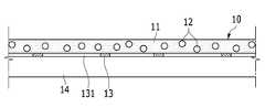
도 1은 본 발명의 제1 실시예에 따른 이방성 도전 필름의 단면도이고, 도 2는 도 1에 도시한 이방성 도전 필름의 평면도이다.FIG. 1 is a cross-sectional view of an anisotropic conductive film according to a first embodiment of the present invention, and FIG. 2 is a plan view of the anisotropic conductive film shown in FIG.
도 1과 도 2를 참고하면, 제1 실시예의 이방성 도전 필름(10)은 접착층(11), 도전 입자들(12), 지지층(13), 및 이형지(14)를 포함한다. 도전 입자들(12)은 접착층(11) 내부에 분산되어 있으며, 지지층(13)은 접착층(11)을 필름 형태로 유지시킨다. 이형지(14)는 지지층(13)의 일면에 위치한다.1 and 2, the anisotropic
보다 구체적으로, 접착층(11)은 열 압착에 의해 연질화되었다가 소정 온도에서 경화되는 절연성 고분자 수지로 이루어진다. 예를 들어, 접착층(11)은 열 경화성 고분자 수지, 열 가소성 고분자 수지, 라디칼 중합성 고분자 수지, 또는 고무계 수지 중합체 중 어느 하나를 포함할 수 있다.More specifically, the
열 경화성 고분자 수지로는 에폭시(epoxy) 수지, 페놀(phenol) 수지, 멜라멘(melamine) 수지 등이 있다. 열 가소성 고분자 수지로는 스티렌 부타디엔(styrene butadiene) 수지, 에틸렌 비닐(ethylene vinyl) 수지, 에스테르(ester) 수지, 실리콘(silicone) 수지, 페녹시(phenoxy) 수지, 아크릴(acryl) 수지, 아미드(amide)계 수지, 비닐부티랄(vinylbutyral) 수지 등이 있다.Thermosetting polymer resins include epoxy resins, phenol resins, and melamine resins. Examples of the thermoplastic polymer resin include styrene butadiene resin, ethylene vinyl resin, ester resin, silicone resin, phenoxy resin, acryl resin, amide ) -Based resin, and a vinylbutyral resin.
라디칼 중합성 수지로는 메틸아크릴레이트(methyacrylate), 에틸아크릴레이트(ethylacrylate), 비스페놀 A 에틸렌글리콜 변성 디아크릴레이트(bisphenaol A ethyleneglycol modified diacrylate) 등이 있다. 고무계 수지 중합체로는 아크릴로니트릴(acrylonitrile)계, 스티렌 부타디엔(styrene butadiene)계, 네오프렌(neoprene)계, 스티렌아크릴로니트릴(styrene acrylonitrile)계, 부타디엔(butadiene)계 등의 고무계 수지의 중합체가 있다.Examples of the radical polymerizable resin include methyacrylate, ethylacrylate, and bisphenol A ethyleneglycol modified diacrylate. Examples of the rubber-based resin polymer include polymers of rubber-based resins such as acrylonitrile, styrene butadiene, neoprene, styrene acrylonitrile, butadiene, and the like .
또한, 접착층(11)은 필요에 따라 충전제, 연화제, 착색제, 난연화제, 광안정제, 가교제 등의 첨가제를 더 포함할 수 있다.The
도전 입자들(12)은 전기적 도통을 위한 것으로서, 접착층(11) 내부에 고르게 분산되어 위치한다. 도전 입자들(12)은 금속 입자로 구성되거나 절연성 물질을 핵으로 하여 표면을 금속으로 피복시킨 입자 등으로 구성될 수 있다. 이때 금속으로는 니켈(Ni), 철(Fe), 구리(Cu), 알루미늄(Al), 주석(Sn), 아연(Zn), 크롬(Cr), 코발트(Co), 금(Au), 또는 은(Ag) 등이 사용될 수 있다.The
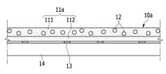
도 3은 도 1에 도시한 이방성 도전 필름의 변형예를 나타낸 단면도이다.3 is a cross-sectional view showing a modified example of the anisotropic conductive film shown in Fig.
도 3을 참고하면, 접착층(11a)은 도전 입자들(12)이 분산되어 위치하는 제1층(111)과, 도전 입자들(12)이 위치하지 않는 제2층(112)으로 구성될 수 있다. 이 경우 이방성 도전 필름(10a)의 접착력을 강화시키며, 보다 안정적인 접속을 수행할 수 있다.3, the
다시 도 1과 도 2를 참고하면, 지지층(13)은 접착층(11)의 일면에 위치하는 일정 두께의 절연층으로 형성된다. 지지층(13)은 복수의 개구부(131)를 가지는 그물망 형태로 이루어진다. 복수의 개구부(131) 각각은 도전 입자(12)보다 크게 형성된다. 예를 들어, 개구부(131) 각각의 크기는 도전 입자(12) 직경의 10배 내지 20배 범위로 설정될 수 있다.Referring back to FIGS. 1 and 2, the
접착층(11)과 그 내부에 분산된 도전 입자들(12)은 열 압착 과정에서 지지층(13)의 개구부(131)를 채운다. 따라서 이형지(14)가 제거된 이후 이방성 도전 필름(10)의 열 압착 과정에서 표시 패널의 전극과 칩 온 필름(chip on film, COF)의 전극은 개구부(131)에 위치한 도전 입자들(12)에 의해 전기적으로 접속되고, 개구부(131)를 채운 접착층(11) 물질에 의해 물리적으로 접착될 수 있다.The
지지층(13)의 개구부(131)는 원형, 삼각형, 사각형, 오각형 이상의 다각형 등 다양한 모양으로 형성될 수 있다. 도 2에서는 육각형의 개구부(131)를 가진 육각 그물망 형태의 지지층(13)을 예로 들어 도시하였다.The
지지층(13)의 내열 온도는 접착층(11)의 열 경화 온도보다 높다. 따라서 지지층(13)은 이방성 도전 필름(10)의 열 압착 공정에 영향을 받지 않으며, 최초 형태를 그대로 유지할 수 있다. 지지층(13)은 180℃ 이상의 내열 온도를 가지는 고 내열성 수지로 형성될 수 있다.The heat resistant temperature of the
예를 들어, 지지층(13)은 폴리페닐렌 설파이드(polyphenylene sulfide), 폴리에테르에테르케톤(polyetheretherketone), 폴리프탈아미드(polyphthalamide), 열가소성 폴리이미드(thermoplastic polyimide), 폴리술폰(polysulfone), 폴리에테르술폰(polyethersulfone), 및 폴리에테르이미드(polyetherimide) 중 어느 하나를 포함할 수 있다.For example, the
전술한 지지층(13)은 표시 패널과 칩 온 필름 사이에 잔류한다. 지지층(13)은 절연 물질로 형성되어 표시 패널과 칩 온 필름의 전기적 접속에 영향을 미치지 않으며, 미세 폭의 그물망 형태로 구성됨에 따라 표시 패널과 칩 온 필름의 물리적 접착에도 실질적인 영향을 미치지 않는다.The
또한, 지지층(13)은 촘촘한 그물망 구조로 인해 스스로 일정한 장력을 보유한다. 이로써 이형지(14)가 제거된 이후에도 접착층(11)은 지지층(13)에 의해 필름 형태를 유지할 수 있으므로 취급이 가능해진다. 즉 통상의 이방성 도전 필름은 이형지 없이 접착층만으로 필름 형태를 유지할 수 없었으며, 이로 인해 본압착 공정 이전 가압착 공정을 거쳐야 했다.Further, the
그러나 제1 실시예의 이방성 도전 필름(10)은 지지층(13)으로 인해 이형지(14) 없이도 접착층(11)을 필름 형태로 유지할 수 있으므로, 이형지(14) 제거 이후 접착층(11)의 취급이 가능해진다. 따라서 제1 실시예의 이방성 도전 필름(10)은 가압착 단계 없이 본압착 공정만으로 표시 패널과 칩 온 필름을 연결할 수 있다. 이방성 도전 필름(10)을 이용한 표시 패널과 칩 온 필름의 연결 과정에 대해서는 후술한다.However, since the anisotropic
도 4는 본 발명의 제2 실시예에 따른 이방성 도전 필름의 단면도이다.4 is a cross-sectional view of an anisotropic conductive film according to a second embodiment of the present invention.
도 4를 참고하면, 제2 실시예의 이방성 도전 필름(10b)은 지지층(132)이 접착층(11)의 일면 전체에 형성됨과 아울러 열 압착시 가해지는 압력에 의해 파단되는 것을 제외하고 전술한 제1 실시예와 같은 구성으로 이루어진다. 제1 실시예와 같은 부재에 대해서는 같은 도면 부호를 사용한다.4, the anisotropic
지지층(132)은 이형지(14)를 향한 접착층(11)의 일면 전체에 위치하여 이형지(14)가 제거된 면에 접착층(11) 물질이 드러나지 않도록 한다. 또한, 지지층(132)은 스스로 일정한 장력을 유지하여 이형지(14)가 제거된 이후 접착층(11)이 필름 형태를 유지하도록 한다. 따라서 이방성 도전 필름(10b)은 이형지(14) 제거 이후 접착층(11)의 취급이 가능하게 되어 가압착 단계를 생략할 수 있다.The
또한, 지지층(132)은 열 압착시 가해지는 압력에 의해 파단되어 도전 입자들(12)과 접착층(11) 물질이 지지층(132)을 관통하도록 한다. 예를 들어, 지지층(132)은 2MPa 내지 3MPa의 파단 압력을 가지는 절연층으로 형성될 수 있다.In addition, the
따라서 이형지(14)가 제거된 이후 이방성 도전 필름(10b)의 열 압착 과정에서 지지층(132)이 파단되면서 도전 입자들(12)과 접착층(11) 물질이 지지층(132)을 관통한다. 그 결과, 표시 패널의 전극과 칩 온 필름의 전극은 지지층(132)을 관통한 도전 입자들(12)에 의해 전기적으로 접속되고, 지지층(132)을 관통한 접착층(11) 물질에 의해 물리적으로 접착된다.Therefore, in the process of thermally compressing the anisotropic
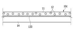
도 5는 본 발명의 제3 실시예에 따른 이방성 도전 필름의 단면도이다.5 is a cross-sectional view of an anisotropic conductive film according to a third embodiment of the present invention.
도 5를 참고하면, 제3 실시예의 이방성 도전 필름(10c)은 지지층(133)이 열 압착시 가해지는 열에 의해 융해되는 것을 제외하고 전술한 제2 실시예와 같은 구성으로 이루어진다. 제2 실시예와 같은 부재에 대해서는 같은 도면 부호를 사용한다.Referring to Fig. 5, the anisotropic
지지층(133)은 열 압착시 가해지는 열에 의해 융해되어 소멸된다. 즉 지지층(133)은 접착층(11)의 열 경화 온도보다 낮은 융해 온도를 가지는 고분자 수지로 형성된다. 예를 들어 지지층(133)은 접착층(11)의 열 경화 온도인 160℃ 내지 180℃보다 낮은 융해 온도를 가지는 저융점 고분자 수지로 형성될 수 있다.The
지지층(133)은 실온에서 일정한 장력을 유지하여 이형지(14)가 제거된 이후 접착층(11)이 필름 형태를 유지하도록 하는 반면 열 압착 과정에서는 열에 의해 융해되어 소멸된다. 따라서 표시 패널의 전극과 칩 온 필름의 전극은 도전 입자들(12)에 의해 전기적으로 접속되고, 접착층(11) 물질에 의해 물리적으로 접착된다.The
전술한 제1 실시예 내지 제3 실시예의 이방성 도전 필름(10, 10b, 10c)에서 지지층(13, 132, 133)은 공통적으로 접착층(11)의 일면에 위치하며, 표시 패널과 칩 온 필름의 전기적 접속 및 물리적 접착에 영향을 미치지 않으면서 일정한 장력을 유지하여 이형지(14)가 제거된 이후 접착층(11)을 필름 형태로 유지시키는 기능을 한다.In the anisotropic
도 6은 본 발명의 일 실시예에 따른 표시 장치의 제조 방법을 나타낸 공정 순서도이다.6 is a flow chart illustrating a method of manufacturing a display device according to an embodiment of the present invention.
도 6을 참고하면, 본 실시예에 따른 표시 장치의 제조 방법은 이방성 도전 필름을 준비하는 제1 단계(S10)와, 이방성 도전 필름에서 이형지를 제거하는 제2 단계(S20)와, 접착층과 지지층을 표시 패널의 제1 패드부 위에 배치하는 제3 단계(S30)와, 접착층과 지지층 위로 칩 온 필름의 제2 패드부를 배치한 다음 접착층과 지지층을 열 압착하여 제1 패드부와 제2 패드부를 접착 및 접속하는 제4 단계(S40)를 포함한다.Referring to FIG. 6, a method of manufacturing a display device according to the present embodiment includes a first step (S10) of preparing an anisotropic conductive film, a second step (S20) of removing a release paper from the anisotropic conductive film, A second pad portion of the chip on film is disposed on the adhesive layer and the support layer, and then the adhesive layer and the support layer are thermally bonded to each other to form a first pad portion and a second pad portion, And a fourth step (S40) of bonding and connecting.
제1 단계(S10)에서 이방성 도전 필름은 접착층, 도전 입자들, 지지층, 및 이형지를 포함하며, 전술한 제1 실시예 내지 제3 실시예 중 어느 한 실시예의 구성으로 이루어진다.In the first step S10, the anisotropic conductive film includes the adhesive layer, the conductive particles, the support layer, and the release paper, and has the configuration of any one of the first to third embodiments described above.
제2 단계(S20)에서 지지층으로부터 이형지가 분리된다. 이때 지지층은 이형지가 분리된 면으로 접착층 물질이 노출되지 않도록 하면서 자체적으로 일정한 장력을 보유한다. 따라서 이형지가 제거된 이후에도 접착층은 지지층에 의해 필름 형태를 유지할 수 있으며, 작업자의 손이나 자동화 공정의 기계 장치에서 이동 및 운반과 같은 취급이 가능해진다.In the second step S20, the release paper is separated from the support layer. At this time, the support layer has a self-sustaining tension so that the adhesive layer material is not exposed to the separated surface of the release paper. Therefore, even after the releasing paper has been removed, the adhesive layer can be kept in the form of a film by the supporting layer, and it becomes possible to handle such as moving and carrying in a machine of an operator's hand or an automation process.
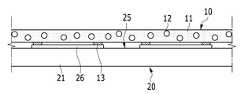
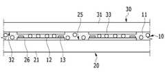
도 7과 도 8은 각각 도 6에 도시한 제3 단계의 표시 패널과 이방성 도전 필름을 개략적으로 나타낸 단면도와 평면도이다.7 and 8 are a cross-sectional view and a plan view schematically showing the display panel of the third step and the anisotropic conductive film shown in Fig. 6, respectively.
도 7과 도 8을 참고하면, 제3 단계(S30)에서 접착층(11)과 지지층(13)은 작업자의 손이나 자동화 공정의 기계 장치에 의해 이송되어 표시 패널(20)의 제1 패드부(25) 위에 배치된다. 제1 패드부(25)는 제1 기판(21) 상에 서로간 거리를 두고 배치된 복수의 제1 패드 전극(26)으로 구성된다.7 and 8, in the third step S30, the
도 7과 도 8에서는 그물망 형태의 지지층(13)을 구비한 제1 실시예의 이방성 도전 필름(10)을 예로 들어 도시하였다. 그물망 형태의 지지층(13)은 미세 폭으로 형성되므로 지지층(13)으로 인한 접착력 저하나 전기적 접속 성능 저하를 유발하지 않는다.7 and 8 illustrate the anisotropic
도 9는 도 6에 도시한 제4 단계의 표시 장치를 나타낸 단면도이다.9 is a cross-sectional view showing the display device of the fourth step shown in Fig.
도 9를 참고하면, 제4 단계(S40)에서 접착층(11)과 지지층(13) 위로 칩 온 필름(30)의 제2 패드부(32)가 배치된다. 제2 패드부(32)는 베이스 필름(31) 상에 서로간 거리를 두고 배치된 복수의 출력측 배선 전극(33)으로 구성된다. 제1 패드 전극(26)과 출력측 배선 전극(33)은 서로 같은 피치와 같은 폭을 갖도록 형성되며, 칩 온 필름(30)은 접착층(11) 및 지지층(13) 위에서 출력측 배선 전극(33)이 제1 패드 전극(26)과 일대일로 마주하도록 정렬된다.9, the
이때 칩 온 필름(30)은 테이프 캐리어 패키지(tape carrier package, TCP) 또는 연성 회로기판(flexible printed circuit, FPC)으로 대체될 수도 있다.At this time, the chip-on
이어서 제1 패드부(25)와 제2 패드부(32)로 열과 압력이 가해진다. 그러면 열에 의해 접착층(11)이 연화되고 압력에 의해 눌리면서 접착층(11) 물질이 지지층(13)의 개구부를 채우며, 제1 패드 전극들(26) 사이 및 출력측 배선 전극(33) 사이로 충진된다.Heat and pressure are then applied to the
그리고 도전 입자들(12)이 제1 패드 전극(26)과 출력측 배선 전극(33) 사이에서 두 전극(26, 33)과 접촉하면서 두 전극(26, 33)을 통전시킨다. 이후 접착층(11)이 경화되면서 제1 패드부(25)와 제2 패드부(32) 사이에 견고하게 접착된다. 이러한 열 압착 과정에서 지지층(13)은 접착층(11)의 열 경화 온도보다 높은 내열 온도를 가지므로 열 변형 없이 초기 상태를 그대로 유지할 수 있다.The
도 10은 도 6에 도시한 제4 단계의 다른 실시예를 나타낸 단면도이다.10 is a cross-sectional view showing another embodiment of the fourth step shown in Fig.
도 10을 참고하면, 표시 장치가 제2 실시예의 이방성 도전 필름(10b)을 구비하는 경우, 제4 단계의 열 압착 과정에서 지지층(132)이 파단되면서 도전 입자들(12)과 접착층(11) 물질이 지지층(132)을 관통한다. 제4 단계의 열 압착은 160℃ 내지 180℃의 온도 및 2MPa 내지 3MPa의 압력 조건에서 10초 내지 20초 가량 진행될 수 있다.10, when the display device includes the anisotropic
따라서 지지층(132)을 관통한 도전 입자들(12)이 제1 패드 전극(26) 및 출력측 배선 전극(33)과 접촉하면서 두 전극(26, 33)을 통전시킨다. 또한, 지지층(132)을 관통한 접착층(11) 물질이 출력측 배선 전극들(33) 사이로 충진되면서 제1 패드부(25) 및 제2 패드부(32)에 견고하게 접착된다.The
도 11은 도 6에 도시한 제4 단계의 또 다른 실시예를 나타낸 단면도이다.11 is a cross-sectional view showing still another embodiment of the fourth step shown in Fig.
도 11을 참고하면, 표시 장치가 제3 실시예의 이방성 도전 필름(10c)을 구비한 경우, 제4 단계의 열 압착 과정에서 지지층(133)이 열에 의해 융해되어 소멸된다. 따라서 열 압착 과정에서 도전 입자들(12)이 제1 패드 전극(26) 및 출력측 배선 전극(33)과 접촉하면서 두 전극(26, 33)을 접속시키고, 접착층(11) 물질이 제1 패드 전극들(26) 사이 및 출력측 배선 전극들(33) 사이에 충진되어 제1 패드부(25) 및 제2 패드부(32)에 견고하게 접착된다.Referring to Fig. 11, when the display device includes the anisotropic
전술한 표시 장치의 제조 방법에 따르면, 종래의 가압착 공정을 생략할 수 있으므로 전체 본딩 공정을 간소화하고, 접착제의 선(先)경화로 인한 접착 불량을 방지할 수 있다. 또한, 이형지가 제거된 이방성 도전 필름이 외부 환경에 노출되는 시간을 최소화할 수 있으므로 이물 유입에 따른 접속 불량도 효과적으로 방지할 수 있다.According to the above-described manufacturing method of the display device, since the conventional pressing and pressing process can be omitted, the entire bonding process can be simplified and adhesion failure due to pre-curing of the adhesive can be prevented. In addition, since the time during which the anisotropic conductive film from which the releasing paper is removed can be exposed to the external environment can be minimized, it is possible to effectively prevent connection failure due to foreign matter inflow.
한편, 상기에서는 이방성 도전 필름(10, 10b, 10c)을 이용한 표시 패널(20)과 칩 온 필름(30)의 연결 방법에 대해 설명하였으나, 칩 온 필름(30)과 인쇄 회로 기판을 연결할 때에도 전술한 방법이 그대로 적용될 수 있다.Although the connection method of the
도 12는 본 발명의 일 실시예에 따른 표시 장치의 부분 단면도이다.12 is a partial cross-sectional view of a display device according to an embodiment of the present invention.
도 12를 참고하면, 본 실시예에 따른 표시 장치(100)는 표시 패널(20)과, 표시 패널(20)로 제어 신호는 보내는 제어 회로가 형성된 인쇄 회로 기판(40)과, 표시 패널(20)과 인쇄 회로 기판(40)을 연결시키는 칩 온 필름(30)을 포함한다. 칩 온 필름(30)은 전술한 테이프 캐리어 패키지 또는 연성 회로 기판으로 대체될 수도 있다.12, the
또한, 표시 장치(100)는 표시 패널(20)의 제1 패드부(25)와 칩 온 필름(30)의 제2 패드부(32) 사이에 위치하는 제1 이방성 도전 필름(110)과, 칩 온 필름(30)의 제3 패드부(34)와 인쇄 회로 기판(40)의 제4 패드부(41) 사이에 위치하는 제2 이방성 도전 필름(120)을 포함한다. 제1 이방성 도전 필름(110)과 제2 이방성 도전 필름(120)은 열 압착 공정이 완료된 이후의 상태를 의미한다.The
표시 패널(20)은 제1 기판(21)과 제2 기판(22)을 포함하며, 제2 기판(22)으로 노출되지 않은 제1 기판(21)의 가장자리에 제1 패드 전극들(26)이 배치된 제1 패드부(25)가 위치한다. 표시 패널(20)은 유기 발광 다이오드를 구비한 유기 발광 표시 패널이거나, 액정층과 컬러 필터층을 구비한 액정 표시 패널일 수 있다. 유기 발광 표시 패널과 액정 표시 패널은 공지 기술이므로 자세한 설명은 생략한다.The
칩 온 필름(30)은 베이스 필름(31)과, 베이스 필름(31)의 일면에 형성된 배선 패턴(33, 35)과, 배선 패턴(33, 35)에 전기적으로 연결된 반도체 칩(36)과, 배선 패턴(33, 35)의 일부를 덮는 솔더 레지스트(37)를 포함할 수 있다. 배선 패턴(33, 35)은 반도체 칩(36)을 사이에 두고 서로 반대 측에 위치하는 출력측 배선 전극(33)과 입력측 배선 전극(35)으로 구분될 수 있다.The chip-on
칩 온 필름(30)의 일측 가장자리에는 출력측 배선 전극들(33)이 노출된 제2 패드부(32)가 위치하며, 칩 온 필름(30)의 반대측 가장자리에는 입력측 배선 전극들(35)이 노출된 제3 패드부(34)가 위치한다. 인쇄 회로 기판(40)의 제4 패드부(41)에는 제2 패드 전극들(42)이 위치한다. 칩 온 필름(30)은 휘어지는 성질을 지니므로 인쇄 회로 기판(40)이 표시 패널(20)의 후면에 위치하도록 구부러질 수 있다.The
제1 이방성 도전 필름(110)은 도 9와 도 10 및 도 11에 도시한 이방성 도전 필름(10, 10b, 10c) 중 어느 하나의 구성으로 이루어진다. 제1 이방성 도전 필름(110)은 제1 패드부(25)의 제1 패드 전극들(26)과 제2 패드부(32)의 출력측 배선 전극들(33)을 접속 및 접착시킨다.The first anisotropic
도 9의 경우, 제1 패드부(25)와 제2 패드부(32) 사이에 접착층(11) 및 도전 입자들(12)과 더불어 그물망 모양의 지지층(13)이 위치한다. 도 10의 경우, 제1 패드부(25)와 제2 패드부(32) 사이에 접착층(11) 및 도전 입자들(12)과 더불어 압력에 의해 파단된 지지층(132)이 위치한다. 도 11의 경우, 제1 패드부(25)와 제2 패드부(32) 사이에 접착층(11)과 도전 입자들(12)이 위치한다.9, a mesh-
제2 이방성 도전 필름(120)은 도 9와 도 10 및 도 11에 도시한 이방성 도전 필름(10, 10b, 10c) 중 어느 하나의 구성으로 이루어진다. 제2 이방성 도전 필름(110)은 제3 패드부(34)의 입력측 배선 전극들(35)과 제4 패드부(41)의 제2 패드 전극들(42)을 접속 및 접착시킨다.The second anisotropic
도 9의 경우, 제3 패드부(34)와 제4 패드부(41) 사이에 접착층(11) 및 도전 입자들(12)과 더불어 그물망 모양의 지지층(13)이 위치한다. 도 10의 경우, 제3 패드부(34)와 제4 패드부(41) 사이에 접착층(11) 및 도전 입자들(12)과 더불어 압력에 의해 파단된 지지층(132)이 위치한다. 도 11의 경우, 제3 패드부(34)와 제4 패드부(41) 사이에 접착층(11)과 도전 입자들(12)이 위치한다.9, a mesh-
상기에서는 본 발명의 바람직한 실시예에 대하여 설명하였지만, 본 발명은 이에 한정되는 것이 아니고 특허청구범위와 발명의 상세한 설명 및 첨부한 도면의 범위 안에서 여러 가지로 변형하여 실시하는 것이 가능하고 이 또한 본 발명의 범위에 속하는 것은 당연하다.While the present invention has been described in connection with what is presently considered to be practical exemplary embodiments, it is to be understood that the invention is not limited to the disclosed embodiments, but, on the contrary, Of course.
10, 10a, 10b, 10c: 이방성 도전 필름
11: 접착층12: 도전 입자들
13, 132, 133: 지지층14: 이형지
20: 표시 패널25: 제1 패드부
30: 칩 온 필름32: 제2 패드부
34: 제3 패드부40: 인쇄 회로 기판
41: 제4 패드부10, 10a, 10b, 10c: Anisotropic conductive film
11: Adhesive layer 12: Conductive particles
13, 132, 133: support layer 14: release paper
20: display panel 25: first pad portion
30: chip on film 32: second pad portion
34: third pad part 40: printed circuit board
41: fourth pad portion
Claims (19)
Translated fromKorean상기 접착층의 내부에 분산되어 위치하는 도전 입자들;
상기 접착층의 일면에 위치하며 상기 접착층을 필름 형태로 유지시키는 지지층; 및
상기 지지층의 일면에 위치하는 이형지
를 포함하는 이방성 도전 필름.An adhesive layer formed of a polymer resin;
Conductive particles dispersed in the adhesive layer;
A support layer located on one side of the adhesive layer and holding the adhesive layer in a film form; And
A release layer disposed on one surface of the support layer,
≪ / RTI >
상기 지지층은 복수의 개구부를 가진 그물망 형태로 이루어지는 이방성 도전 필름.The method according to claim 1,
Wherein the support layer is in the form of a net having a plurality of openings.
상기 복수의 개구부 각각은 상기 도전 입자의 직경보다 크게 형성되는 이방성 도전 필름.3. The method of claim 2,
Wherein each of the plurality of openings is formed larger than the diameter of the conductive particles.
상기 지지층의 내열 온도는 상기 고분자 수지의 열 경화 온도보다 높은 이방성 도전 필름.3. The method of claim 2,
Wherein the heat resistant temperature of the support layer is higher than the heat curing temperature of the polymer resin.
상기 지지층은 폴리페닐렌 설파이드, 폴리에테르에테르케톤, 폴리프탈아미드, 열가소성 폴리이미드, 폴리술폰, 폴리에테르술폰, 및 폴리에테르이미드 중 어느 하나를 포함하는 이방성 도전 필름.5. The method of claim 4,
Wherein the support layer comprises any one of polyphenylene sulfide, polyether ether ketone, polyphthalamide, thermoplastic polyimide, polysulfone, polyether sulfone, and polyether imide.
상기 지지층은 2MPa 내지 3MPa의 파단 압력을 가지는 절연층으로 형성되는 이방성 도전 필름.The method according to claim 1,
Wherein the supporting layer is formed of an insulating layer having a breaking pressure of 2 MPa to 3 MPa.
상기 지지층은 상기 고분자 수지의 열 경화 온도보다 낮은 융해 온도를 가지는 절연층으로 형성되는 이방성 도전 필름.The method according to claim 1,
Wherein the support layer is formed of an insulating layer having a melting temperature lower than a thermal curing temperature of the polymer resin.
상기 접착층은,
상기 고분자 수지에 상기 도전 입자들이 분산되어 있는 제1층; 및
상기 고분자 수지만으로 구성된 제2층
을 포함하는 이방성 도전 필름.8. The method according to any one of claims 1 to 7,
The adhesive layer
A first layer in which the conductive particles are dispersed in the polymer resin; And
A second layer composed only of the polymer resin
≪ / RTI >
상기 이방성 도전 필름에서 상기 이형지를 제거하는 단계;
상기 접착층과 상기 지지층을 표시 패널의 제1 패드부 위에 배치하는 단계; 및
상기 접착층과 상기 지지층 위로 칩 온 필름의 제2 패드부를 배치하고, 상기 접착층과 상기 지지층을 열 압착하여 상기 제1 패드부와 상기 제2 패드부를 접속 및 접착하는 단계
를 포함하는 표시 장치의 제조 방법.Preparing an anisotropic conductive film comprising conductive particles dispersed in the adhesive layer, a support layer disposed on one surface of the adhesive layer to maintain the adhesive layer in a film form, and a release sheet disposed on one surface of the support layer;
Removing the release paper from the anisotropic conductive film;
Disposing the adhesive layer and the supporting layer on the first pad portion of the display panel; And
A second pad portion of the chip-on film is disposed on the adhesive layer and the support layer, and the adhesive layer and the support layer are thermally bonded to each other to connect and bond the first pad portion and the second pad portion
And a step of forming the display device.
상기 지지층은 복수의 개구부를 가진 그물망 형태로 이루어지며,
상기 지지층의 내열 온도는 상기 접착층의 열 경화 온도보다 높은 표시 장치의 제조 방법.10. The method of claim 9,
Wherein the support layer is in the form of a mesh having a plurality of openings,
Wherein the heat resistant temperature of the support layer is higher than the heat curing temperature of the adhesive layer.
상기 열 압착 과정에서 상기 접착층 물질이 상기 복수의 개구부를 채우며,
상기 복수의 개구부에서 상기 도전 입자들이 상기 제1 패드부의 전극과 상기 제2 패드부의 전극 사이에 위치하는 표시 장치의 제조 방법.11. The method of claim 10,
Wherein the adhesive layer material fills the plurality of openings in the thermocompression process,
Wherein the conductive particles in the plurality of openings are positioned between the electrodes of the first pad portion and the electrodes of the second pad portion.
상기 지지층은 2MPa 내지 3MPa의 파단 압력을 가지며, 상기 열 압착 과정에서 파단되어 상기 접착층 물질과 상기 도전 입자들이 상기 지지층을 관통하는 표시 장치의 제조 방법.10. The method of claim 9,
Wherein the support layer has a breaking pressure of 2 MPa to 3 MPa and is broken in the thermocompression bonding process so that the adhesive layer material and the conductive particles pass through the support layer.
상기 지지층은 상기 접착층의 열 경화 온도보다 낮은 융해 온도를 가지며, 상기 열 압착 과정에서 융해되어 소멸되는 표시 장치의 제조 방법.10. The method of claim 9,
Wherein the support layer has a melting temperature lower than a thermal curing temperature of the adhesive layer, and is melted after the thermal compression process.
상기 제1 패드부와 마주하는 제2 패드부를 구비하는 칩 온 필름; 및
상기 제1 패드부와 상기 제2 패드부 사이에 위치하여 상기 제1 패드부와 상기 제2 패드부를 접속 및 접착시키는 제1 이방성 도전 필름을 포함하며,
상기 제1 이방성 도전 필름은,
고분자 수지로 형성된 접착층;
상기 제1 패드부와 상기 제2 패드부를 접속시키는 도전 입자들; 및
상기 접착층의 일면에 위치하는 지지층
을 포함하는 표시 장치.A display panel having a first pad portion;
A chip on film having a second pad portion facing the first pad portion; And
And a first anisotropic conductive film disposed between the first pad portion and the second pad portion to connect and bond the first pad portion and the second pad portion,
The first anisotropic conductive film may have a thickness
An adhesive layer formed of a polymer resin;
Conductive particles connecting the first pad portion and the second pad portion; And
A support layer disposed on one surface of the adhesive layer,
.
상기 지지층은 상기 고분자 수지로 채워진 복수의 개구부를 형성하는 그물망 형태로 이루어지는 표시 장치.15. The method of claim 14,
Wherein the support layer is in the form of a net to form a plurality of openings filled with the polymer resin.
상기 지지층은 복수의 파단 개구부를 형성하며,
상기 고분자 수지와 상기 도전 입자들은 상기 복수의 파단 개구부에서 상기 지지층을 관통하는 표시 장치.15. The method of claim 14,
The supporting layer forming a plurality of breaking openings,
Wherein the polymer resin and the conductive particles pass through the supporting layer at the plurality of breaking openings.
상기 칩 온 필름은 제3 패드부를 형성하고,
상기 표시 장치는,
상기 제3 패드부와 마주하는 제4 패드부를 구비하는 인쇄 회로 기판; 및
상기 제3 패드부와 상기 제4 패드부 사이에 위치하여 상기 제3 패드부와 상기 제4 패드부를 접속 및 접착시키는 제2 이방성 도전 필름을 더 포함하며,
상기 제2 이방성 도전 필름은,
고분자 수지로 형성된 접착층;
상기 제3 패드부와 상기 제4 패드부를 접속시키는 도전 입자들; 및
상기 접착층의 일면에 위치하는 지지층
을 포함하는 표시 장치.15. The method of claim 14,
The chip-on film forms a third pad portion,
The display device includes:
And a fourth pad portion facing the third pad portion; And
And a second anisotropic conductive film positioned between the third pad and the fourth pad to connect and bond the third pad and the fourth pad,
The second anisotropic conductive film may have a thickness
An adhesive layer formed of a polymer resin;
Conductive particles connecting the third pad portion and the fourth pad portion; And
A support layer disposed on one surface of the adhesive layer,
.
상기 지지층은 상기 고분자 수지로 채워진 복수의 개구부를 형성하는 그물망 형태로 이루어지는 표시 장치.18. The method of claim 17,
Wherein the support layer is in the form of a net to form a plurality of openings filled with the polymer resin.
상기 지지층은 복수의 파단 개구부를 형성하며,
상기 고분자 수지와 상기 도전 입자들은 상기 복수의 파단 개구부에서 상기 지지층을 관통하는 표시 장치.18. The method of claim 17,
The supporting layer forming a plurality of breaking openings,
Wherein the polymer resin and the conductive particles pass through the supporting layer at the plurality of breaking openings.
Priority Applications (2)
| Application Number | Priority Date | Filing Date | Title |
|---|---|---|---|
| KR1020130025114AKR20140110553A (en) | 2013-03-08 | 2013-03-08 | Anisotropic conductive film, display device, and manufacturing method of display device |
| US14/201,112US20140254119A1 (en) | 2013-03-08 | 2014-03-07 | Anisotropic conductive film, display device, and manufacturing method of display device |
Applications Claiming Priority (1)
| Application Number | Priority Date | Filing Date | Title |
|---|---|---|---|
| KR1020130025114AKR20140110553A (en) | 2013-03-08 | 2013-03-08 | Anisotropic conductive film, display device, and manufacturing method of display device |
Publications (1)
| Publication Number | Publication Date |
|---|---|
| KR20140110553Atrue KR20140110553A (en) | 2014-09-17 |
Family
ID=51487558
Family Applications (1)
| Application Number | Title | Priority Date | Filing Date |
|---|---|---|---|
| KR1020130025114AWithdrawnKR20140110553A (en) | 2013-03-08 | 2013-03-08 | Anisotropic conductive film, display device, and manufacturing method of display device |
Country Status (2)
| Country | Link |
|---|---|
| US (1) | US20140254119A1 (en) |
| KR (1) | KR20140110553A (en) |
Families Citing this family (10)
| Publication number | Priority date | Publication date | Assignee | Title |
|---|---|---|---|---|
| CN203206586U (en)* | 2013-02-27 | 2013-09-18 | 奥特斯(中国)有限公司 | A semi-finished product used for producing a printed circuit board |
| US10219384B2 (en) | 2013-11-27 | 2019-02-26 | At&S Austria Technologie & Systemtechnik Aktiengesellschaft | Circuit board structure |
| AT515101B1 (en) | 2013-12-12 | 2015-06-15 | Austria Tech & System Tech | Method for embedding a component in a printed circuit board |
| AT515447B1 (en) | 2014-02-27 | 2019-10-15 | At & S Austria Tech & Systemtechnik Ag | Method for contacting a component embedded in a printed circuit board and printed circuit board |
| US11523520B2 (en) | 2014-02-27 | 2022-12-06 | At&S Austria Technologie & Systemtechnik Aktiengesellschaft | Method for making contact with a component embedded in a printed circuit board |
| KR102304102B1 (en)* | 2015-01-14 | 2021-09-23 | 삼성디스플레이 주식회사 | Display device |
| CN107230444B (en)* | 2017-07-05 | 2020-11-03 | 张家港康得新光电材料有限公司 | Maintenance device of 3D display screen |
| KR102629350B1 (en)* | 2018-12-12 | 2024-01-25 | 삼성디스플레이 주식회사 | Display device and manufacturing method thereof |
| KR20200145985A (en)* | 2019-06-21 | 2020-12-31 | 삼성디스플레이 주식회사 | Display device and method of manufacturing display device |
| KR20220124309A (en)* | 2021-03-02 | 2022-09-14 | 삼성디스플레이 주식회사 | Adhesive member, display device, and manufacturing method of display device |
Family Cites Families (4)
| Publication number | Priority date | Publication date | Assignee | Title |
|---|---|---|---|---|
| FR2726397B1 (en)* | 1994-10-28 | 1996-11-22 | Commissariat Energie Atomique | ANISOTROPIC CONDUCTIVE FILM FOR MICROCONNECTICS |
| US6487002B1 (en)* | 2001-06-11 | 2002-11-26 | Xerox Corporation | Large area micro-structure template for creation of closely packed arrays |
| US7078095B2 (en)* | 2004-07-07 | 2006-07-18 | Xerox Corporation | Adhesive film exhibiting anisotropic electrical conductivity |
| US8802214B2 (en)* | 2005-06-13 | 2014-08-12 | Trillion Science, Inc. | Non-random array anisotropic conductive film (ACF) and manufacturing processes |
- 2013
- 2013-03-08KRKR1020130025114Apatent/KR20140110553A/ennot_activeWithdrawn
- 2014
- 2014-03-07USUS14/201,112patent/US20140254119A1/ennot_activeAbandoned
Also Published As
| Publication number | Publication date |
|---|---|
| US20140254119A1 (en) | 2014-09-11 |
Similar Documents
| Publication | Publication Date | Title |
|---|---|---|
| KR20140110553A (en) | Anisotropic conductive film, display device, and manufacturing method of display device | |
| JP6726070B2 (en) | Electronic component mounting method, electronic component joining structure, substrate device, display device, display system | |
| KR101975730B1 (en) | Anisotropic conductive film, method for producing anisotropic conductive film, method for producing connection body, and connection method | |
| JP4123998B2 (en) | Electronic circuit device and manufacturing method thereof | |
| EP1763295A2 (en) | Electronic component embedded board and its manufacturing method | |
| JPH03131089A (en) | How to connect the circuit board | |
| CN1411329A (en) | Circuit substrate connecting structure, liquid crystal display with same and mounting method | |
| KR100713333B1 (en) | Multilayer anisotropic conductive film | |
| JP6679320B2 (en) | Connection body manufacturing method, electronic component connection method | |
| JP2014146650A (en) | Wiring board and manufacturing method of the same | |
| JP4041649B2 (en) | Electronic component mounting method and electronic component mounting body | |
| CN105493279A (en) | System for attaching devices to flexible substrates | |
| KR20180035132A (en) | Mounting Method Of Electronic Component, Bonding Structure Of Electronic Component, Substrate Device, Display Device, And Display System | |
| TWI581972B (en) | A method of manufacturing a connecting body, and a method of connecting an electronic component | |
| KR100807352B1 (en) | Electrode having a plurality of protrusions on the electrode pad, an electronic device having a component mounting structure having the same and a method of mounting the components of the electronic device | |
| JP6370562B2 (en) | CONNECTION MANUFACTURING METHOD, FLEXIBLE BOARD CONNECTION METHOD, CONNECTION BODY AND FLEXIBLE SUBSTRATE | |
| JP6783537B2 (en) | Manufacturing method of the connector | |
| KR101008824B1 (en) | Semiconductor device having an electrode to which polymer particles are attached and semiconductor package using the same | |
| JP2007250619A5 (en) | ||
| JP2007035546A (en) | Press-bonding device and method | |
| JP5485510B2 (en) | Electronic device, electronic apparatus, and method of manufacturing electronic device | |
| KR102860690B1 (en) | Display device and manufacturing method thereof | |
| KR100646068B1 (en) | Anisotropic conductive film | |
| KR20090106777A (en) | Flexible circuit board and tape carrier package with electrodes with conductive particles attached | |
| KR100766181B1 (en) | Multilayer anisotropic conductive film |
Legal Events
| Date | Code | Title | Description |
|---|---|---|---|
| PA0109 | Patent application | Patent event code:PA01091R01D Comment text:Patent Application Patent event date:20130308 | |
| PG1501 | Laying open of application | ||
| PC1203 | Withdrawal of no request for examination | ||
| WITN | Application deemed withdrawn, e.g. because no request for examination was filed or no examination fee was paid |