KR20140110137A - Touch display apparatus and method of manufacturing the same - Google Patents
Touch display apparatus and method of manufacturing the sameDownload PDFInfo
- Publication number
- KR20140110137A KR20140110137AKR1020130022707AKR20130022707AKR20140110137AKR 20140110137 AKR20140110137 AKR 20140110137AKR 1020130022707 AKR1020130022707 AKR 1020130022707AKR 20130022707 AKR20130022707 AKR 20130022707AKR 20140110137 AKR20140110137 AKR 20140110137A
- Authority
- KR
- South Korea
- Prior art keywords
- wiring connection
- semiconductor
- forming
- base substrate
- pattern
- Prior art date
- Legal status (The legal status is an assumption and is not a legal conclusion. Google has not performed a legal analysis and makes no representation as to the accuracy of the status listed.)
- Withdrawn
Links
Images


Classifications
- H—ELECTRICITY
- H10—SEMICONDUCTOR DEVICES; ELECTRIC SOLID-STATE DEVICES NOT OTHERWISE PROVIDED FOR
- H10K—ORGANIC ELECTRIC SOLID-STATE DEVICES
- H10K59/00—Integrated devices, or assemblies of multiple devices, comprising at least one organic light-emitting element covered by group H10K50/00
- H10K59/40—OLEDs integrated with touch screens
- G—PHYSICS
- G02—OPTICS
- G02F—OPTICAL DEVICES OR ARRANGEMENTS FOR THE CONTROL OF LIGHT BY MODIFICATION OF THE OPTICAL PROPERTIES OF THE MEDIA OF THE ELEMENTS INVOLVED THEREIN; NON-LINEAR OPTICS; FREQUENCY-CHANGING OF LIGHT; OPTICAL LOGIC ELEMENTS; OPTICAL ANALOGUE/DIGITAL CONVERTERS
- G02F1/00—Devices or arrangements for the control of the intensity, colour, phase, polarisation or direction of light arriving from an independent light source, e.g. switching, gating or modulating; Non-linear optics
- G02F1/01—Devices or arrangements for the control of the intensity, colour, phase, polarisation or direction of light arriving from an independent light source, e.g. switching, gating or modulating; Non-linear optics for the control of the intensity, phase, polarisation or colour
- G02F1/13—Devices or arrangements for the control of the intensity, colour, phase, polarisation or direction of light arriving from an independent light source, e.g. switching, gating or modulating; Non-linear optics for the control of the intensity, phase, polarisation or colour based on liquid crystals, e.g. single liquid crystal display cells
- G02F1/133—Constructional arrangements; Operation of liquid crystal cells; Circuit arrangements
- G02F1/1333—Constructional arrangements; Manufacturing methods
- G02F1/13338—Input devices, e.g. touch panels
- G—PHYSICS
- G02—OPTICS
- G02F—OPTICAL DEVICES OR ARRANGEMENTS FOR THE CONTROL OF LIGHT BY MODIFICATION OF THE OPTICAL PROPERTIES OF THE MEDIA OF THE ELEMENTS INVOLVED THEREIN; NON-LINEAR OPTICS; FREQUENCY-CHANGING OF LIGHT; OPTICAL LOGIC ELEMENTS; OPTICAL ANALOGUE/DIGITAL CONVERTERS
- G02F1/00—Devices or arrangements for the control of the intensity, colour, phase, polarisation or direction of light arriving from an independent light source, e.g. switching, gating or modulating; Non-linear optics
- G02F1/01—Devices or arrangements for the control of the intensity, colour, phase, polarisation or direction of light arriving from an independent light source, e.g. switching, gating or modulating; Non-linear optics for the control of the intensity, phase, polarisation or colour
- G02F1/13—Devices or arrangements for the control of the intensity, colour, phase, polarisation or direction of light arriving from an independent light source, e.g. switching, gating or modulating; Non-linear optics for the control of the intensity, phase, polarisation or colour based on liquid crystals, e.g. single liquid crystal display cells
- G02F1/133—Constructional arrangements; Operation of liquid crystal cells; Circuit arrangements
- G02F1/136—Liquid crystal cells structurally associated with a semi-conducting layer or substrate, e.g. cells forming part of an integrated circuit
- G02F1/1362—Active matrix addressed cells
- G02F1/136204—Arrangements to prevent high voltage or static electricity failures
- G—PHYSICS
- G02—OPTICS
- G02F—OPTICAL DEVICES OR ARRANGEMENTS FOR THE CONTROL OF LIGHT BY MODIFICATION OF THE OPTICAL PROPERTIES OF THE MEDIA OF THE ELEMENTS INVOLVED THEREIN; NON-LINEAR OPTICS; FREQUENCY-CHANGING OF LIGHT; OPTICAL LOGIC ELEMENTS; OPTICAL ANALOGUE/DIGITAL CONVERTERS
- G02F1/00—Devices or arrangements for the control of the intensity, colour, phase, polarisation or direction of light arriving from an independent light source, e.g. switching, gating or modulating; Non-linear optics
- G02F1/01—Devices or arrangements for the control of the intensity, colour, phase, polarisation or direction of light arriving from an independent light source, e.g. switching, gating or modulating; Non-linear optics for the control of the intensity, phase, polarisation or colour
- G02F1/13—Devices or arrangements for the control of the intensity, colour, phase, polarisation or direction of light arriving from an independent light source, e.g. switching, gating or modulating; Non-linear optics for the control of the intensity, phase, polarisation or colour based on liquid crystals, e.g. single liquid crystal display cells
- G02F1/133—Constructional arrangements; Operation of liquid crystal cells; Circuit arrangements
- G02F1/136—Liquid crystal cells structurally associated with a semi-conducting layer or substrate, e.g. cells forming part of an integrated circuit
- G02F1/1362—Active matrix addressed cells
- G02F1/136209—Light shielding layers, e.g. black matrix, incorporated in the active matrix substrate, e.g. structurally associated with the switching element
- G—PHYSICS
- G06—COMPUTING OR CALCULATING; COUNTING
- G06F—ELECTRIC DIGITAL DATA PROCESSING
- G06F3/00—Input arrangements for transferring data to be processed into a form capable of being handled by the computer; Output arrangements for transferring data from processing unit to output unit, e.g. interface arrangements
- G06F3/01—Input arrangements or combined input and output arrangements for interaction between user and computer
- G06F3/03—Arrangements for converting the position or the displacement of a member into a coded form
- G06F3/041—Digitisers, e.g. for touch screens or touch pads, characterised by the transducing means
- G06F3/0412—Digitisers structurally integrated in a display
- G—PHYSICS
- G06—COMPUTING OR CALCULATING; COUNTING
- G06F—ELECTRIC DIGITAL DATA PROCESSING
- G06F3/00—Input arrangements for transferring data to be processed into a form capable of being handled by the computer; Output arrangements for transferring data from processing unit to output unit, e.g. interface arrangements
- G06F3/01—Input arrangements or combined input and output arrangements for interaction between user and computer
- G06F3/03—Arrangements for converting the position or the displacement of a member into a coded form
- G06F3/041—Digitisers, e.g. for touch screens or touch pads, characterised by the transducing means
- G06F3/042—Digitisers, e.g. for touch screens or touch pads, characterised by the transducing means by opto-electronic means
- H—ELECTRICITY
- H10—SEMICONDUCTOR DEVICES; ELECTRIC SOLID-STATE DEVICES NOT OTHERWISE PROVIDED FOR
- H10F—INORGANIC SEMICONDUCTOR DEVICES SENSITIVE TO INFRARED RADIATION, LIGHT, ELECTROMAGNETIC RADIATION OF SHORTER WAVELENGTH OR CORPUSCULAR RADIATION
- H10F39/00—Integrated devices, or assemblies of multiple devices, comprising at least one element covered by group H10F30/00, e.g. radiation detectors comprising photodiode arrays
- H10F39/10—Integrated devices
- H10F39/12—Image sensors
- H10F39/198—Contact-type image sensors [CIS]
- H—ELECTRICITY
- H10—SEMICONDUCTOR DEVICES; ELECTRIC SOLID-STATE DEVICES NOT OTHERWISE PROVIDED FOR
- H10F—INORGANIC SEMICONDUCTOR DEVICES SENSITIVE TO INFRARED RADIATION, LIGHT, ELECTROMAGNETIC RADIATION OF SHORTER WAVELENGTH OR CORPUSCULAR RADIATION
- H10F55/00—Radiation-sensitive semiconductor devices covered by groups H10F10/00, H10F19/00 or H10F30/00 being structurally associated with electric light sources and electrically or optically coupled thereto
- H10F55/10—Radiation-sensitive semiconductor devices covered by groups H10F10/00, H10F19/00 or H10F30/00 being structurally associated with electric light sources and electrically or optically coupled thereto wherein the radiation-sensitive semiconductor devices control the electric light source, e.g. image converters, image amplifiers or image storage devices
- H—ELECTRICITY
- H10—SEMICONDUCTOR DEVICES; ELECTRIC SOLID-STATE DEVICES NOT OTHERWISE PROVIDED FOR
- H10K—ORGANIC ELECTRIC SOLID-STATE DEVICES
- H10K59/00—Integrated devices, or assemblies of multiple devices, comprising at least one organic light-emitting element covered by group H10K50/00
- H10K59/10—OLED displays
- H10K59/12—Active-matrix OLED [AMOLED] displays
- H10K59/1201—Manufacture or treatment
- G—PHYSICS
- G02—OPTICS
- G02F—OPTICAL DEVICES OR ARRANGEMENTS FOR THE CONTROL OF LIGHT BY MODIFICATION OF THE OPTICAL PROPERTIES OF THE MEDIA OF THE ELEMENTS INVOLVED THEREIN; NON-LINEAR OPTICS; FREQUENCY-CHANGING OF LIGHT; OPTICAL LOGIC ELEMENTS; OPTICAL ANALOGUE/DIGITAL CONVERTERS
- G02F1/00—Devices or arrangements for the control of the intensity, colour, phase, polarisation or direction of light arriving from an independent light source, e.g. switching, gating or modulating; Non-linear optics
- G02F1/01—Devices or arrangements for the control of the intensity, colour, phase, polarisation or direction of light arriving from an independent light source, e.g. switching, gating or modulating; Non-linear optics for the control of the intensity, phase, polarisation or colour
- G02F1/13—Devices or arrangements for the control of the intensity, colour, phase, polarisation or direction of light arriving from an independent light source, e.g. switching, gating or modulating; Non-linear optics for the control of the intensity, phase, polarisation or colour based on liquid crystals, e.g. single liquid crystal display cells
- G02F1/133—Constructional arrangements; Operation of liquid crystal cells; Circuit arrangements
- G02F1/13306—Circuit arrangements or driving methods for the control of single liquid crystal cells
- G02F1/13312—Circuits comprising photodetectors for purposes other than feedback
- G—PHYSICS
- G02—OPTICS
- G02F—OPTICAL DEVICES OR ARRANGEMENTS FOR THE CONTROL OF LIGHT BY MODIFICATION OF THE OPTICAL PROPERTIES OF THE MEDIA OF THE ELEMENTS INVOLVED THEREIN; NON-LINEAR OPTICS; FREQUENCY-CHANGING OF LIGHT; OPTICAL LOGIC ELEMENTS; OPTICAL ANALOGUE/DIGITAL CONVERTERS
- G02F2202/00—Materials and properties
- G02F2202/10—Materials and properties semiconductor
- G—PHYSICS
- G02—OPTICS
- G02F—OPTICAL DEVICES OR ARRANGEMENTS FOR THE CONTROL OF LIGHT BY MODIFICATION OF THE OPTICAL PROPERTIES OF THE MEDIA OF THE ELEMENTS INVOLVED THEREIN; NON-LINEAR OPTICS; FREQUENCY-CHANGING OF LIGHT; OPTICAL LOGIC ELEMENTS; OPTICAL ANALOGUE/DIGITAL CONVERTERS
- G02F2203/00—Function characteristic
- G02F2203/11—Function characteristic involving infrared radiation
- G—PHYSICS
- G06—COMPUTING OR CALCULATING; COUNTING
- G06F—ELECTRIC DIGITAL DATA PROCESSING
- G06F2203/00—Indexing scheme relating to G06F3/00 - G06F3/048
- G06F2203/041—Indexing scheme relating to G06F3/041 - G06F3/045
- G06F2203/04103—Manufacturing, i.e. details related to manufacturing processes specially suited for touch sensitive devices
Landscapes
- Physics & Mathematics (AREA)
- Engineering & Computer Science (AREA)
- Nonlinear Science (AREA)
- General Physics & Mathematics (AREA)
- Crystallography & Structural Chemistry (AREA)
- Chemical & Material Sciences (AREA)
- Mathematical Physics (AREA)
- Optics & Photonics (AREA)
- General Engineering & Computer Science (AREA)
- Theoretical Computer Science (AREA)
- Microelectronics & Electronic Packaging (AREA)
- Human Computer Interaction (AREA)
- Manufacturing & Machinery (AREA)
- Devices For Indicating Variable Information By Combining Individual Elements (AREA)
- Liquid Crystal (AREA)
Abstract
Translated fromKoreanDescription
Translated fromKorean본 발명은 터치 표시 장치 및 이의 제조 방법에 관한 것으로, 더욱 상세하게는 정전기를 방지하는 터치 표시 장치 및 정전기를 방지할 수 있는 터치 표시 장치의 제조 방법에 관한 것이다.The present invention relates to a touch display device and a method of manufacturing the touch display device, and more particularly, to a touch display device for preventing static electricity and a method for manufacturing a touch display device capable of preventing static electricity.
최근, 소형, 경량화의 장점을 가지고 있는 평판 표시 장치가 주목받고 있다. 상기 평판표시 장치에는 LCD(liquid crystal display), OELD(organic electro luminescence display) 등이 있다.In recent years, flat panel display devices having advantages of small size and light weight have been attracting attention. The flat panel display includes a liquid crystal display (LCD), an organic electro luminescence display (OELD), and the like.
이러한 평판 표시 장치의 제조 공정은 대부분 유리 기판 등의 기판 상에서 수행되는데, 이러한 기판은 부도체이므로 순간적으로 발생하는 전하가 기판의 아래로 방전될 수 없어서 정전기에 매우 취약하다. 따라서, 상기 기판상에 형성된 절연막, TFT 또는 발광소자가 정전기에 의해 손상될 수 있다. 또한, 정전기에 의해 터치 패널에서 센서 구동시 가로줄 불량이 발현된다. 이는 게이트 입력단에서 발생하는 정전기가 원인이다.The fabrication process of such a flat panel display device is mostly performed on a substrate such as a glass substrate. Since such a substrate is non-conductive, an instantaneous charge can not be discharged below the substrate and is very vulnerable to static electricity. Therefore, the insulating film, TFT, or light emitting element formed on the substrate may be damaged by static electricity. In addition, when the sensor is driven in the touch panel by static electricity, a line defect is generated. This is caused by static electricity generated at the gate input terminal.
따라서, 종래에 정전기를 방지하기 위한 것으로서 스캔 라인 또는 데이터 라인의 끝부분에 다수의 스캔 라인 또는 데이터 라인을 각각 하나로 묶는 정전기 방지 배선을 형성하였다. 상기 정전기 방지 배선은 각각의 셀에 신호를 인가하여 평판 표시장치를 작동하기 위하여 단선(컷팅)되어야 한다. 이를 위해, 게이트 라인을 묶어 가드링을 형성하여 정전기 문제의 해결을 시도하였다. 그러나 종래의 정전기 방지 방법은 금속이 노출되어 공정 진행 중 부식의 우려가 있으며, 상기 가드링을 제거하는 공정에서 게이트 라인이 손상될 수 있어 표시장치의 품질이 저하되는 문제점이 있다.Therefore, in order to prevent static electricity, an anti-static wiring is formed to connect a plurality of scan lines or data lines to the ends of the scan lines or the data lines. The anti-static wiring must be disconnected (cut) to operate the flat panel display by applying a signal to each cell. For this purpose, we tried to solve the static electricity problem by bundling the gate lines and forming the guard ring. However, in the conventional static electricity prevention method, the metal is exposed and there is a risk of corrosion during the process. In the process of removing the guard ring, the gate line may be damaged and the quality of the display device is deteriorated.
이에, 본 발명의 기술적 과제는 이러한 점에서 착안된 것으로 본 발명의 목적은 정전기를 방지할 수 있는 터치 표시 장치를 제공하는 것이다.SUMMARY OF THE INVENTION Accordingly, the present invention has been made in view of the above problems, and it is an object of the present invention to provide a touch display device capable of preventing static electricity.
본 발명의 다른 목적은 상기 터치 표시 장치의 제조 방법을 제공하는 것이다.Another object of the present invention is to provide a manufacturing method of the touch display device.
상기한 본 발명의 목적을 실현하기 위한 일 실시예에 따른 터치 표시 장치는 베이스 기판, 상기 베이스 기판 위에 배치되고, 가시광은 차단하고 적외선 광을 투과하는 반도체 차광패턴, 상기 반도체 차광패턴 위에 배치되며, 입사되는 적외선 광에 대응하여 위치를 검출하는 센싱 소자, 상기 센싱 소자를 구동하기 위한 구동 소자, 상기 센싱 소자 또는 구동 소자와 전기적으로 연결되면 일 방향으로 연장되는 신호라인 및 상기 반도체 차광 패턴과 동일한 물질을 포함하며, 신호 라인의 아래에 배치되는 배선 연결부를 포함한다.According to another aspect of the present invention, there is provided a touch display device including a base substrate, a semiconductor light-shielding pattern disposed on the base substrate and shielding visible light and transmitting infrared light, A driving element for driving the sensing element, a signal line extending in one direction when electrically connected to the sensing element or the driving element, and a signal line extending in the same direction as the semiconductor light- And a wiring connection portion disposed below the signal line.
본 발명의 일 실시예에 있어서, 상기 반도체 차광 패턴은 비정질-실리콘게르마늄(a-SiGe)을 포함할 수 있다.In one embodiment of the present invention, the semiconductor light shielding pattern may include amorphous-silicon germanium (a-SiGe).
본 발명의 일 실시예에 있어서, 상기 센싱 소자는 상기 반도체 차광패턴 위에 배치된 반도체 패턴, 상기 반도체 패턴의 일단과 중첩하는 소스 전극, 상기 소스 전극과 이격되며, 상기 반도체 패턴의 타단과 중첩하는 드레인 전극 및 상기 소스 전극 및 드레인 전극 위에 배치된 게이트 전극을 포함할 수 있다.In one embodiment of the present invention, the sensing element may include a semiconductor pattern disposed on the semiconductor light-shielding pattern, a source electrode overlapping one end of the semiconductor pattern, a drain spaced apart from the source electrode, And a gate electrode disposed on the source electrode and the drain electrode.
본 발명의 일 실시예에 있어서, 상기 배선 연결부는 비정질-실리콘게르마늄(a-SiGe)을 포함할 수 있다.In one embodiment of the present invention, the wiring connection portion may include amorphous-silicon germanium (a-SiGe).
본 발명의 일 실시예에 있어서, 상기 반도체 차광 패턴과 상기 배선 연결부는 동일한 층에 형성될 수 있다.In one embodiment of the present invention, the semiconductor light shielding pattern and the wiring connection portion may be formed on the same layer.
상기한 본 발명의 목적을 실현하기 위한 다른 실시예에 따른 터치 표시 장치의 제조방법은 베이스 기판상에 가시광은 차단하고 적외선 광을 투과하는 반도체 차광 패턴, 상기 반도체 차광 패턴과 동일한 물질을 포함하며, 표시 영역에 배치되는 배선 연결부, 상기 표시 영역을 둘러싸는 주변 영역상에 배치되며, 상기 배선 연결부와 연결되는 가드링을 포함하는 반도체 층을 형성하는 단계, 상기 배선 연결부 위에 배치되어 일 방향으로 연장되는 신호 라인을 포함하는 금속 패턴을 형성하는 단계 및 상기 금속 패턴이 형성된 베이스 기판 상에, 입사되는 적외선 광에 대응하여 위치를 검출하기 위한 센싱 소자를 형성하는 단계를 포함한다.According to another aspect of the present invention, there is provided a method of manufacturing a touch display device including a base substrate, a semiconductor light shielding pattern blocking visible light and transmitting infrared light, and a material identical to the semiconductor light shielding pattern, Forming a semiconductor layer including a wiring connection portion disposed in a display region, a guard ring disposed on a peripheral region surrounding the display region and connected to the wiring connection portion, forming a semiconductor layer on the wiring connection portion, Forming a metal pattern including a signal line and a sensing element for detecting a position corresponding to incident infrared light on the base substrate on which the metal pattern is formed.
본 발명의 일 실시예에 있어서, 상기 센싱소자를 형성하는 단계는In one embodiment of the present invention, the step of forming the sensing element comprises
상기 반도체 차광 패턴이 형성된 베이스 기판 상에 반도체 패턴을 형성하는 단계, 상기 반도체 패턴이 형성된 베이스 기판 상에 소스 전극 및 드레인 전극을 형성하는 단계, 상기 소스 전극 및 드레인 전극이 형성된 베이스 기판 상에 절연층을 형성하는 단계 및 상기 절연층이 형성된 베이스 기판 상에 게이트 전극을 형성하는 단계를포함할수 있다.Forming a semiconductor pattern on the base substrate on which the semiconductor light shielding pattern is formed; forming a source electrode and a drain electrode on the base substrate on which the semiconductor pattern is formed; And forming a gate electrode on the base substrate on which the insulating layer is formed.
본 발명의 일 실시예에 있어서, 상기 반도체 층은 비정질-실리콘게르마늄을 포함할 수 있다.In one embodiment of the present invention, the semiconductor layer may comprise amorphous-silicon germanium.
본 발명의 일 실시예에 있어서, 상기 금속 패턴은 상기 주변 영역 상에 배치되며, 상기 신호 라인과 교차하는 방향으로 연장되는 공통전압배선 및 상기 주변 영역 상에 배치되며, 상기 신호 라인 및 상기 배선 연결부와 이격되는 패드부를 포함할 수 있다.In one embodiment of the present invention, the metal pattern is disposed on the peripheral region, and includes a common voltage wiring extending in a direction crossing the signal line, and a common voltage wiring disposed on the peripheral region, And a pad portion spaced apart from the pad portion.
본 발명의 일 실시예에 있어서, 상기 배선 연결부는 상기과 상기 신호 라인을 연결하며, 상기 가드링과 상기 패드부를 연결할 수 있다.In one embodiment of the present invention, the wiring connection part connects the signal line and the guard ring, and connects the guard ring and the pad part.
본 발명의 일 실시예에 있어서, 상기 절연층을 형성하는 단계에서 상기 가드링 및 상기 배선 연결부의 일부가 제거될 수 있다.In one embodiment of the present invention, in the step of forming the insulating layer, a part of the guard ring and the wiring connection part may be removed.
본 발명의 일 실시예에 있어서, 상기 신호 라인과 상기 패드부가 연결하는 연결 전극을 형성하는 단계를 더 포함하며, 상기 연결 전극은 상기 게이트 전극과 동일한 공정에서 형성될 수 있다.According to an embodiment of the present invention, the method may further include forming a connection electrode connecting the signal line and the pad portion, wherein the connection electrode may be formed in the same process as the gate electrode.
상기한 본 발명의 목적을 실현하기 위한 또 다른 실시예에 따른 터치 표시 장치의 제조방법은 베이스 기판 상에 가시광은 차단하고 적외선광을 투과하는 반도체 차광 패턴 및 상기 반도체 차광 패턴과 동일한 물질을 포함하며 표시 영역에 배치되는 배선 연결부를 포함하는 반도체 층을 형성하는 단계, 상기 배선 연결부 위에 배치되어 일 방향으로 연장되는 신호 라인을 포함하는 금속 패턴을 형성하는 단계 및 상기 게이트 금속 패턴이 형성된 베이스 기판 상에, 입사되는 적외선 광에 대응하여 위치를 검출하기 위한 센싱 소자를 형성하는 단계를 포함한다.According to another aspect of the present invention, there is provided a method of manufacturing a touch display device including a base substrate on which a visible light is shielded, a semiconductor light shielding pattern transmitting infrared light, and a material same as the semiconductor light shielding pattern, Forming a semiconductor layer including a wiring connection portion disposed in a display region, forming a metal pattern that is disposed on the wiring connection portion and includes signal lines extending in one direction, And forming a sensing element for detecting the position corresponding to the incident infrared light.
본 발명의 일 실시예에 있어서, 상기 센싱소자를 형성하는 단계는In one embodiment of the present invention, the step of forming the sensing element comprises
상기 반도체 차광 패턴이 형성된 베이스 기판 상에 반도체 패턴을 형성하는 단계, 상기 반도체 패턴이 형성된 베이스 기판 상에 소스 전극 및 드레인 전극을 형성하는 단계, 상기 소스 전극 및 드레인 전극이 형성된 베이스 기판 상에 절연층을 형성하는 단계 및 상기 절연층이 형성된 베이스 기판 상에 게이트 전극을 형성하는 단계를 포함할 수 있다.Forming a semiconductor pattern on the base substrate on which the semiconductor light shielding pattern is formed; forming a source electrode and a drain electrode on the base substrate on which the semiconductor pattern is formed; And forming a gate electrode on the base substrate on which the insulating layer is formed.
본 발명의 일 실시예에 있어서, 상기 반도체 층은 비정질-실리콘게르마늄을 포함할 수 있다.In one embodiment of the present invention, the semiconductor layer may comprise amorphous-silicon germanium.
본 발명의 일 실시예에 있어서, 상기 금속 패턴은 상기 주변 영역 상에 배치되며, 상기 신호 라인과 교차하는 방향으로 연장되는 공통전압배선 및 상기 주변 영역 상에 배치되며, 상기 신호 라인 및 상기 배선 연결부와 이격되는 패드부를 포함할 수 있다.In one embodiment of the present invention, the metal pattern is disposed on the peripheral region, and includes a common voltage wiring extending in a direction crossing the signal line, and a common voltage wiring disposed on the peripheral region, And a pad portion spaced apart from the pad portion.
본 발명의 일 실시예에 있어서, 상기 배선 연결부는 상기 신호 라인과 상기 패드부 사이를 연결할 수 있다.In one embodiment of the present invention, the wiring connection portion may connect between the signal line and the pad portion.
본 발명의 일 실시예에 있어서, 상기 절연층을 형성하는 단계에서 상기 배선 연결부의 일부가 제거될 수 있다.In one embodiment of the present invention, a part of the wiring connection portion may be removed in the step of forming the insulation layer.
본 발명의 일 실시예에 있어서, 상기 신호 라인과 상기 패드부를 연결하는 연결전극을 형성하는 단계를 더 포함하며, 상기 연결 전극은 상기 게이트 전극과 동일한 공정에서 형성될 수 있다.According to an embodiment of the present invention, the method may further include forming a connection electrode connecting the signal line and the pad portion, wherein the connection electrode may be formed in the same process as the gate electrode.
본 발명의 일 실시예에 있어서, 상기 배선 연결부는 상기 신호 라인과 상기 패드부 사이의 일부 영역에 상기 신호 라인 및 상기 패드부와 분리되어 형성될 수 있다.In one embodiment of the present invention, the wiring connection part may be formed separately from the signal line and the pad part in a part of the space between the signal line and the pad part.
이와 같은 터치 표시 장치 및 이의 제조방법에 따르면, 밴드 패스 필터 물질을 포함하는 가드링 및 배선 연결부를 이용하여, 게이트 라인 및 패드부 사이에서 정전기가 발생하지 않게 되고, 표시장치의 표시 품질을 향상시킬 수 있다.According to such a touch display device and its manufacturing method, static electricity is not generated between the gate line and the pad portion by using the guard ring and the wiring connection portion including the band-pass filter material, and the display quality of the display device is improved .
또한, 가드링이 밴드 패스 필터 물질을 이용하여 형성되므로 공정의 추가 없이 정전기를 방지할 수 있으며, 가드링 제거 공정에서 게이트 라인의 손상이 발생되지 않는다.In addition, since the guard ring is formed using the band-pass filter material, static electricity can be prevented without adding a process, and damage to the gate line in the guard ring removing process does not occur.
도 1은 본 발명의 일 실시예에 따른 터치 표시 장치에 가드링이 형성된 상태를 개략적으로 나타내는 평면도이다.
도 2는 도 1의 A 부분을 확대한 평면도이다.
도 3은 도 1의 B 부분을 확대한 평면도이다.
도 4는 본 발명의 일 실시예에 따른 터치 표시 장치의 단위 화소를 나타내는 평면도이다.
도 5는 도 도 1의 II-II' 라인 및 도 2의 I-I' 라인을 따라 절단한 단면도이다.
도 6a 내지 6e는 도 5의 터치 표시 장치의 제조방법을 설명하기 위한 단면도들이다.
도 7은 본 발명의 다른 실시예에 따른 터치 표시장치의 단면도이다.
도 8a 내지 8e는 도 7의 터치 표시 장치의 제조방법을 설명하기 위한 단면도들이다.
도 9는 본 발명의 또 다른 실시예에 따른 터치 표시장치의 단면도이다.
도 10a 내지 10e는 도 9의 터치 표시 장치의 제조방법을 설명하기 위한 단면도들이다.1 is a plan view schematically showing a guard ring formed on a touch display device according to an embodiment of the present invention.
2 is an enlarged plan view of a portion A in Fig.
3 is an enlarged plan view of a portion B in Fig.
4 is a plan view showing a unit pixel of a touch display device according to an embodiment of the present invention.
5 is a cross-sectional view taken along line II-II 'of FIG. 1 and line II' of FIG.
6A to 6E are cross-sectional views illustrating a method of manufacturing the touch display device of FIG.
7 is a cross-sectional view of a touch display device according to another embodiment of the present invention.
8A to 8E are cross-sectional views illustrating a method of manufacturing the touch display device of FIG.
9 is a cross-sectional view of a touch display device according to another embodiment of the present invention.
10A to 10E are cross-sectional views for explaining the manufacturing method of the touch display device of FIG.
이하, 첨부한 도면들을 참조하여, 본 발명의 바람직한 실시예를 보다 상세하게 설명하고자 한다.Hereinafter, preferred embodiments of the present invention will be described in detail with reference to the accompanying drawings.
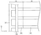
도 1은 본 발명의 일 실시예에 따른 터치 표시 장치에 가드링이 형성된 상태를 개략적으로 나타내는 평면도이다.1 is a plan view schematically showing a guard ring formed on a touch display device according to an embodiment of the present invention.
도 1을 참조하면, 도 1은 본 발명의 일 실시예에 따른 터치 표시 장치의 제조 단계에서 가드링(201)이 형성된 상태를 나타낸다. 상기 가드링은 표시 패널의 표시 영역(DA)을 둘러싸는 폐쇄된 사각형 형태로 주변 영역(PA)에 형성된다. 상기 가드링(201)은 터치 표시 장치가 제조되는 공정상에서 제거되므로, 완성된 터치 표시 장치에서는 존재하지 않는다. 표시 영역(DA) 내에는 스위칭 박막 트랜지스터 및 구동 박막 트랜지스터가 형성될 수 있다.1, a
도 2는 도 1의 A 부분을 확대한 평면도이다.2 is an enlarged plan view of a portion A in Fig.
도 2를 참조하면, 본 발명의 일 실시예에 따른 터치 표시 장치는 반도체층(200), 공통전압배선(302) 및 게이트 라인(301)을 포함한다. 상기 반도체층(200)은 가드링(201) 및 배선 연결부(202)를 포함한다. 상기 가드링(201)은 주변 영역(PA)에 형성되어 표시 영역(DA)을 둘러싸는 형태로 형성된다. 상기 공통전압배선(302)은 주변 영역(PA)에 형성되며 제1 방향으로 연장된다. 상기 게이트 라인(301)은 표시 영역(DA)에 형성되며 상기 제1 방향과 수직인 제2 방향으로 연장된다.Referring to FIG. 2, the touch display device includes a
완성된 터치 표시 장치에는 존재하지 않으나 본 발명의 일 실시예에 따른 터치 표시장치의 제조 단계에서 상기 가드링(201)이 먼저 형성된다. 상기 가드링(201)은 상기 표시 영역(DA)을 둘러싸는 형태로 형성되어 상기 게이트 라인(301) 및 상기 패드부(303) 사이에 발생되는 전위차를 제거하는 역할을 한다. 상기 가드링(201)은 밴드 패스 필터(Band Pass Filter : BPF) 물질을 포함할 수 있다. 상기 밴드 패스 필터 물질은 터치 패널에서 금속 패턴이 형성된 영역에 배치되어 가시광을 차단하는 차광 패턴(예컨대, Black-Matrix : BM)의 기능과 적외광 센싱 소자의 반도체 패턴이 형성된 영역에 형성되어 특정 파장대역의 광, 즉, 적외광을 투과하는 역할을 한다. 상기 밴드 패스 필터 물질은 비정질 실리콘 게르마늄(a-SiGe)을 포함할 수 있다. 상기 밴드 패스 필터 물질은 광차단 효과를 갖는 물질이지만 상기 밴드 패스 필터 물질은 낮은 저항값을 가지는 특성을 가지고 있다. 따라서 상기 밴드 패스 필터 물질은 본 발명의 일실시예에 따른 터치 표시 장치에서 상기 가드링(201)을 형성하는 재료로 사용되어 배선의 기능을 수행 할 수 있다.Although not present in the completed touch display device, the
상기 배선 연결부(202)는 주변 영역(PA)에 형성되어 상기 가드링(201)과 상기 게이트 라인(301) 사이를 연결한다. 상기 배선 연결부(202)는 상기 가드링(201)과 동일한 물질로 형성될 수 있다.The
도 3은 도 1의 B 부분을 확대한 평면도이다.3 is an enlarged plan view of a portion B in Fig.
도 3을 참조하면, 본 발명의 일 실시예에 따른 터치 표시 장치는 반도체층(200), 패드부(303) 및 게이트 라인(301)을 포함한다. 상기 반도체층(200)은 가드링(201) 및 배선 연결부(202)를 포함한다. 상기 가드링(201)은 주변 영역(PA)에 형성되어 표시 영역(DA)을 둘러싸는 형태로 형성된다. 상기 패드부(303)는 주변 영역(PA)에 형성되며 연결전극에 의해 상기 게이트 라인(301)과 연결된다. 상기 게이트 라인(301)은 표시 영역(DA)에 형성되며 상기 제1 방향과 수직인 제2 방향으로 연장된다.Referring to FIG. 3, the touch display device includes a
상기 배선 연결부(202)는 주변 영역(PA)에 형성되어 상기 가드링(201)과 상기 패드부(302) 사이를 연결한다. 따라서, 상기 가드링(201) 및 상기 배선 연결부(202)에 의해 연결되어 상기 게이트 라인(301)과 상기 패드부(303) 사이는 서로 등전위를 가지게 되므로 정전기가 발생하지 않게 된다. 상기 가드링(201) 및 상기 가드링(201)의 좌측과 상기 공통전압배선(302) 사이, 상기 공통전압배선(302)과 상기 게이트 라인(301) 사이 및 상기 가드링(201)의 우측과 상기 패드부(303) 사이를 연결하는 상기 배선 연결부(202)는 본 발명의 일 실시예에 따른 터치 표시 장치의 제조 단계 중 제2 절연층(404)을 식각하는 과정에서 동시에 식각된다. 따라서, 완성된 본 발명의 일 실시예에 따른 터치 표시장치에서는 상기 가드링(201) 및 상기 가드링(201)의 좌측과 상기 공통전압배선(302) 사이, 상기 공통전압배선(302)과 상기 게이트 라인(301) 및 상기 가드링(201)의 우측과 상기 패드부(303) 사이를 연결하는 상기 배선 연결부(202)는 존재하지 않는다.The
상기 배선 연결부(202)가 형성된 베이스 기판상에 게이트 금속 패턴(300)이 형성된다. 따라서, 상기 게이트 라인(301)은 상기 배선 연결부(202)와 중첩되게 형성되어, 상기 배선 연결부(202)를 통해, 상기 패널의 일 영역에서 상기 게이트 라인(301)과 상기 가드링(201)이 전기적으로 연결되고, 다른 영역에서 상기 가드링(201)과 상기 패드부(303)가 전기적으로 연결되므로 상기 게이트 라인(301)과 상기 패드부(303) 사이의 전위차가 제거된다.A gate metal pattern 300 is formed on the base substrate on which the
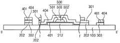
도 4는 본 발명의 일 실시예에 따른 터치 표시 장치의 단위 화소를 나타내는 평면도이다.4 is a plan view showing a unit pixel of a touch display device according to an embodiment of the present invention.
도 4를 참조하면, 발명의 일 실시예에 따른 터치 표시 장치는 신호 라인, 제1 전압 라인(VL1), 제2 전압 라인(VL2), 제1 반도체 차광패턴(210), 제2 반도체 차광패턴(212), 스위칭 소자(TR11), 센싱 소자(TR12) 및 커패시터(242)를 포함할 수 있다. 상기 신호 라인은 게이트 라인(301) 및 바이어스 전압 라인(BVL)을 포함할 수 있다.4, the touch display device includes a signal line, a first voltage line VL1, a second voltage line VL2, a first semiconductor light-
상기 게이트 라인(301)은 제1 방향(D1)으로 연장되어 게이트 신호를 인가한다. 상기 바이어스 전압 라인(BVL)은 상기 제1 방향(D1)으로 연장되어 바이어스 전압을 인가한다.The
상기 제1 전압 라인(VL1)은 상기 제1 방향(D1)과 교차하는 제2 방향(D2)으로 연장되어 제1 전압을 인가한다. 상기 제2 전압 라인(VL2)은 상기 제2 방향(D2)으로 연장되어 상기 제1 전압 라인(VL1)과 인접하게 배치되고, 제2 전압을 인가한다.The first voltage line VL1 extends in a second direction D2 intersecting the first direction D1 to apply a first voltage. The second voltage line VL2 extends in the second direction D2 and is disposed adjacent to the first voltage line VL1 and applies a second voltage.
상기 제1 반도체 차광패턴(210)은 반도체 물질을 포함한다. 예를 들면, 상기 반도체 물질은 비정질 실리콘 게르마늄(a-SiGe)을 포함할 수 있다. 상기 제1 반도체 차광패턴(210)은 상기 스위칭 소자(TR11)가 형성되는 영역에 대응하여 형성된다. 상기 제1 반도체 차광패턴(210)은 상기 스위칭 소자(TR11)로 입사되는 적외선 광은 투과하고 가시광은 차단한다.The first semiconductor
상기 제2 반도체 차광패턴(212)은 상기 비정질 실리콘 게르마늄(a-SiGe)을 포함할 수 있다. 상기 제2 반도체 차광패턴(212)은 상기 센싱 소자(TR12)가 형성되는 영역에 대응하여 형성된다. 상기 제2 반도체 차광패턴(212)은 상기 센싱 소자(TR12)로 입사되는 적외선 광은 투과하고 가시광은 차단한다.The second semiconductor
상기 제1 스위칭 소자(TR11)는 제1 반도체 패턴(230), 제1 소스 전극(SE1), 제1 드레인 전극(DE2) 및 제1 게이트 전극(GE1)을 포함한다.The first switching device TR11 includes a
상기 제1 반도체 패턴(230)은 상기 제1 절연층(401)이 형성된 베이스 기판 위에 상기 제1 반도체 차광패턴(210)과 중첩되게 배치된다. 상기 제1 반도체 패턴(230)은 액티브층 및 오믹 콘택층을 포함하는 이중층으로 형성될 수 있다. 상기 액티브층은 비정질 실리콘(a-Si)을 포함할 수 있다. 상기 오믹 콘택층은 n+ 비정질 실리콘을 포함할 수 있다.The
상기 제1 소스 전극(SE1) 및 제1 드레인 전극(DE1)은 상기 제1 반도체 패턴(230) 위에 서로 이격되어 배치된다. 상기 제1 소스 전극(SE1)은 상기 제1 전압 라인(VL1)과 연결되어 상기 제1 전압을 수신한다.The first source electrode SE1 and the first drain electrode DE1 are spaced apart from each other on the
상기 제1 소스 전극(SE1) 및 상기 제1 드레인 전극(DE1) 위에는 제2 절연층(404)이 배치된다. 상기 제2 절연층(404)에는 상기 제1 반도체 차광패턴(210)을 노출시키는 제1 콘택홀(CNT1)이 형성된다.A second insulating
상기 제1 게이트 전극(GE1)은 상기 제2 절연층(404) 위에 배치된다. 상기 제1 게이트 전극(GE1)은 상기 제1 콘택홀(CNT1)을 통해 상기 제1 반도체 차광패턴(210)과 전기적으로 연결된다. 상기 제1 반도체 차광패턴(210)은 상기 제1 게이트 전극(GE1)을 통해 상기 게이트 신호를 수신한다.The first gate electrode GE1 is disposed on the second insulating
상기 스위칭 소자(TR11)는 상기 제1 반도체 차광패턴(210)과 상기 제1 게이트 전극(GE1)을 포함하는 더블 게이트 구조를 가진다. 상기 스위칭 소자(TFT)는 상기 게이트 라인(301)에 인가되는 게이트 신호에 응답하여 상기 제1 전압 라인(VL1)에 인가되는 상기 제1 전압을 상기 센싱 소자(TR12)에 전달한다.The switching element TR11 has a double gate structure including the first semiconductor
상기 센싱 소자(TR12)는 적외선 광에 기초하여 상기 베이스 기판에 접촉된 물체의 위치를 검출한다. 예를 들면, 상기 센싱 소자(TR12)는 백라이트 어셈블리로부터 발생되어 상기 베이스 기판에 접촉된 상기 물체에 의해 반사된 적외선 광을 이용하여 상기 물체의 위치를 검출한다. 상기 백라이트 어셈블리는 상기 적외선 광을 발생하는 제1 광발생부 및 가시광을 발생하는 제2 광발생부를 포함할 수 있다.The sensing element TR12 detects the position of an object contacting the base substrate based on infrared light. For example, the sensing element TR12 detects the position of the object by using infrared light reflected from the object generated from the backlight assembly and contacting the base substrate. The backlight assembly may include a first light generator for generating the infrared light and a second light generator for generating visible light.
상기 센싱 소자(TR12)는 제2 반도체 패턴(503), 제2 소스 전극(501), 제2 드레인 전극(502) 및 제2 게이트 전극(610)을 포함한다.The sensing element TR12 includes a
상기 제2 반도체 패턴(503)은 상기 제1 절연층(401)이 형성된 베이스 기판 위에 상기 제2 반도체 차광패턴(212)과 중첩되게 배치된다. 상기 제2 반도체 패턴(503)은 비정질 실리콘 게르마늄(a-SiGe)을 포함하는 액티브층 및 n+ 비정질 실리콘을 포함하는 오믹 콘택층을 포함할 수 있다.The
상기 제2 소스 전극(501)은 상기 제2 반도체 패턴(503) 위에 배치되고, 상기 스위칭 소자(TR11)의 상기 제1 드레인 전극(DE1)으로부터 연장된다. 상기 제2 소스 전극(501)은 U자가 반복되는 요철 구조를 형성될 수 있다. 상기 제2 소스 전극(501)을 U자 형으로 형성하면 상기 적외선 광을 수광하기 위한 채널 영역을 넓게 할 수 있으며, 이에 따라서 채널을 통해 이동하는 전하의 이동도를 우수하게 하여 트랜지스터의 전기적 특성을 향상시킬 수 있다.The
상기 제2 드레인 전극(502)은 상기 제2 반도체 패턴(503) 위에 상기 제2 소스 전극(501)과 이격되어 배치되고, 상기 제2 소스 전극(501)에 대응하여 U자가 반복되는 요철 구조를 가질 수 있다.The
상기 제2 소스 전극(501) 및 상기 제2 드레인 전극(502) 위에는 상기 제2 절연층(404)이 배치된다. 상기 제2 절연층(404)은 상기 제2 반도체 차광패턴(212)을 노출시키는 제2 콘택홀(CNT2)을 더 포함한다.The second
상기 제2 게이트 전극(610)은 상기 제2 절연층(404) 위에 배치된다. 상기 제2 게이트 전극(610)은 상기 제2 콘택홀(CNT2)을 통해 상기 제2 반도체 차광패턴(212)과 전기적으로 연결된다. 상기 제2 반도체 차광패턴(212)은 상기 제2 게이트 전극(610)을 통해 게이트 신호를 수신한다.The
상기 센싱 소자(TR12)는 상기 제2 반도체 차광패턴(212)과 상기 제2 게이트 전극(610)을 포함하는 더블 게이트 구조를 가진다.The sensing element TR12 has a double gate structure including the second semiconductor
상기 커패시터(242)는 상기 센싱 소자(TR12)의 상기 제2 소스 전극(501)과 연결된 제1 전극(242a), 및 상기 제2 절연층(404)을 사이에 두고 상기 제1 전극(242a)과 중첩되게 형성되며 상기 바이어스 전압 라인(BVL)과 연결된 제2 전극(242b)을 포함한다. 상기 커패시터(242)는 상기 센싱 소자(TR12)의 상기 액티브층에 수광된 광의 양에 비례하여 전하를 충전하는 역할을 한다.The
상기 제1 게이트 전극(GE1), 제2 게이트 전극(610) 및 커패시터의 제2전극(242b)가 형성된 베이스 기판상에 블랙 매트릭스 패턴을 형성된다. 이어서, 상기 블랙매트릭스 패턴이 형성된 상기 베이스 기판 위에 컬러필터층을 형성한다. 상기 컬러필터층이 형성된 상기 베이스 기판위에 오버 코팅층을 형성한다. 이어서, 상기 오버 코팅층이 형성된 상기 베이스 기판 위에 상기 공통전극을 형성한다. 상기 컬러필터층은 화소 영역들(R, G, B)에 배치된다. 상기 컬러필터층은 적색 컬러필터, 녹색 컬러필터 및 청색 컬러필터를 포함할 수 있다.A black matrix pattern is formed on the base substrate on which the first gate electrode GE1, the
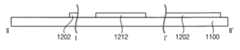
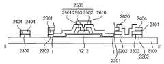
도 5는 도 1의 II-II' 라인 및 도 2의 I-I' 라인을 따라 절단한 단면도이다.5 is a cross-sectional view taken along line II-II 'of FIG. 1 and line I-I' of FIG.
도 5를 참조하면, 베이스 기판(100) 상에 반도체 층(200), 게이트 라인(301), 제1 절연층(401), 센싱 소자(500), 제2 절연층(404), 제2 게이트 전극(610) 및 연결 전극(620)이 형성된다. 상기 베이스 기판(100) 상에 상기 배선 연결부(202)가 형성된다. 상기 반도체 층(200)은 가드링(201), 배선 연결부(202) 및 제2 반도체 차광 패턴(212)을 포함한다. 상기 배선 연결부(202)는 상기 게이트 라인(301)과 중첩되며, 상기 제2 반도체 차광 패턴(212)은 센싱 소자(500)와 중첩한다.5, a
상기 배선 연결부(202)가 형성된 상기 베이스 기판(100) 상에 게이트 라인(301)이 형성된다. 상기 게이트 라인(301)은 제1 방향(D1)으로 연장되며, 게이트 신호를 전달한다. 상기 게이트 라인(301)이 형성된 후, 제1 절연층(401)이 형성되며, 센싱 소자(500)가 순차적으로 형성된다. 상기 센싱 소자(500)는 제2 소스 전극(501), 제2 드레인 전극(502) 및 제2 반도체 패턴(503)을 포함한다. 도면상에는 하나의 센싱 소자(500)만이 도시되었으나, 복수개의 센싱 소자가 형성될 수 있다. 상기 센싱 소자(500)가 형성된 후 제2 절연층(404)이 형성된다. 상기 제2 절연층(404)은 상기 센싱 소자(500)와 제2 게이트 전극(610)을 절연시키는 역할을 한다. 상기 제2 절연층(404) 상에 제2 게이트 전극(610) 및 연결 전극(620)이 형성된다. 상기 연결 전극(620)은 분리되어 있는 상기 게이트 라인(301)과 상기 패드부(303)를 연결하는 역할을 한다. 상기 제2 게이트 전극(610)과 상기 연결 전극(620)은 동일한 층으로 형성된다. 본 실시예에서는 상기 배선 연결부(202)가 상기 게이트 라인(301)과 중첩되는 것을 예를 들어 설명하였으나, 이에 한정되지 않고 상기 배선 연결부(202)는 상기 게이트 라인(301) 및 바이어스 전압라인을 포함하는 신호 라인들과 중첩될 수 있다.A
이하에서는 도면들을 참조하여, 본 발명의 일 실시예에 따른 터치 표시장치의 제조 방법에 대하여 설명한다.Hereinafter, a method of manufacturing a touch display device according to an embodiment of the present invention will be described with reference to the drawings.
도 5는 도 1의 II-II' 라인 및 도 2의 I-I' 라인을 따라 절단한 단면도이다. 도 6a 내지 6e는 도 5의 터치 표시 장치의 제조방법을 설명하기 위한 단면도들이다.5 is a cross-sectional view taken along line II-II 'of FIG. 1 and line I-I' of FIG. 6A to 6E are cross-sectional views illustrating a method of manufacturing the touch display device of FIG.
도 6a를 참조하면, 상기 베이스 기판(100) 상에 반도체 층(200)이 형성된다. 상기 반도체 층(200)은 상기 가드링(201), 상기 배선 연결부(202) 및 제2 반도체 차광 패턴(212)을 포함한다. 상기 가드링(201)은 표시 패널의 외곽을 둘러싸는 사각형 형태로 형성된다.Referring to FIG. 6A, a
상기 배선 연결부(202)는 상기 게이트 라인이 형성되는 위치 및 상기 가드링(201)의 좌측과 상기 공통전압배선(302) 사이, 상기 공통전압배선(302)과 상기 게이트 라인(301) 사이 및 상기 가드링(201)의 우측과 상기 패드부(303) 사이를 연결하도록 형성된다.The
상기 제2 반도체 차광 패턴(212)은 센싱 소자(500)가 형성되는 영역에 형성된다. 상기 제2 반도체 차광 패턴(212)은 밴드패스필터 물질을 포함하여, 가시광은 차단하고 적외선 광은 투과시킬 수 있다.The second semiconductor
도 6b를 참조하면, 상기 가드링(201) 및 상기 배선 연결부(202) 및 상기 제2 반도체 차광 패턴(212)이 형성된 베이스 기판(100) 상에 상기 게이트 금속 패턴(300)이 형성된다. 상기 게이트 금속 패턴(300)은 상기 게이트 라인(301), 상기 공통전압배선(302) 및 상기 패드부(303)를 포함한다.6B, the gate metal pattern 300 is formed on the
상기 게이트 라인(301) 및 상기 공통전압배선(302)은 상기 배선 연결부(202)와 중첩되도록 배치된다. 상기 패드부(303)는 상기 배선 연결부(202)와 중첩되지 않으며, 상기 가드링(201)의 우측과 연결되는 상기 배선 연결부(202)와 접촉하도록 형성된다. 따라서, 상기 게이트 라인(301)과 상기 공통 전압 배선(302)이 전기적으로 연결되고, 상기 패드부(303)는 상기 가드링(201)의 우측과 전기적으로 연결된다. 또한 상기 공통 전압 배선(302)이 상기 가드링(201)의 좌측과 전기적으로 연결되므로, 결과적으로 상기 게이트 라인(301), 상기 공통 전압 배선(302) 및 상기 패드부(303)는 모두 전기적으로 연결된다.The
즉, 상기 가드링(201) 및 상기 배선 연결부(202)는 낮은 저항값을 갖는 밴드 패스 필터 물질로 구성되므로 상기 게이트 금속 패턴(300)을 전기적으로 연결하여 전위를 갖도록 한다. 따라서, 정전기 발생으로 불량이 발생하는 상기 게이트 라인(301) 및 상기 패드부(303) 사이가 서로 등전위를 가지게 되어 정전기가 발생되지 않도록 하는 역할을 한다.That is, since the
도 6c를 참조하면, 상기 게이트 금속 패턴(300)이 형성된 베이스 기판(100) 상에 제1 절연층(401) 및 센싱 소자(500)가 순차적으로 형성된다. 상기 제1 절연층(401)이 형성된 후 상기 제2 반도체 차광 패턴(212)이 형성된 영역에 상기 센싱 소자(500)가 형성된다. 상기 센싱 소자(500)를 형성하는 과정은 건식 식각으로 진행된다. 이 과정에서 정전기가 발생될 수 있으며, 상기 게이트 라인(301) 및 상기 패드부(303) 사이의 전위차로 인해 정전기가 발생된다.Referring to FIG. 6C, a first insulating
그러나 본 발명의 일 실시예에 따른 터치 표시장치에서는 상기 가드링(201) 및 상기 배선 연결부(202)에 의해 상기 게이트 라인(301) 및 상기 패드부(303) 사이가 서로 등전위를 가지게 되어 정전기 발생을 방지할 수 있다.However, in the touch display device according to an embodiment of the present invention, the
도 6d를 참조하면, 상기 센싱 소자(500)가 형성된 베이스 기판(100) 상에 제2 절연층(404)이 형성된다. 상기 제2 절연층(404)은 상기 센싱 소자(500)와 제2 게이트 전극(610)을 절연시킨다. 도 6d는 상기 제2 절연층(404)이 식각되기 전의 상태를 나타낸다. 이후 상기 제2 절연층(404)이 식각되며, 이 과정에서 상기 가드링(201) 및 상기 가드링(201)의 좌측과 상기 공통전압배선(302) 사이, 상기 공통전압배선(302)과 상기 게이트 라인(301) 사이 및 상기 가드링(201)의 우측과 상기 패드부(303) 사이를 연결하는 상기 배선 연결부(202)가 동시에 식각된다.Referring to FIG. 6D, a second insulating
도 6e를 참조하면, 상기 제2 절연층(404)이 형성된 후에, 상기 제2 절연층(404)을 식각한 상태가 나타난다. 상기 제2 절연층(404)을 식각하는 과정에서 상기 가드링(201) 및 상기 가드링(201)의 좌측과 상기 공통전압배선(302) 사이, 상기 공통전압배선(302)과 상기 게이트 라인(301) 사이 및 상기 가드링(201)의 우측과 상기 패드부(303) 사이를 연결하는 상기 배선 연결부(202)가 동시에 식각된다. 따라서, 상기 가드링(201)은 완전히 제거되고 상기 배선 연결부(202)는 일부가 제거된다. 이 때, 상기 배선 연결부(202)는 상기 게이트 라인(301)의 하부 및 상기 공통전압배선(302)의 하부에 남겨진다. 즉, 제2 절연층(404)을 식각하는 과정에서 상기 가드링(201) 및 상기 배선 연결부(202)의 일부가 제거되어 상기 베이스 기판(100) 상에 배선 연결부(202)의 일부가 남겨지고, 상기 게이트 라인(301), 상기 공통전압배선(302), 상기 패드부(303) 및 센싱 소자(500)가 형성된 상태가 나타난다. 이 때, 연결 전극(620)에 의해 연결되기 위한 상기 게이트 라인(301)의 일부 및 상기 패드부(303)의 일부가 노출된다.Referring to FIG. 6E, after the second insulating
다시 도 5를 참조하면, 상기 제2 절연층(404)을 식각하는 과정에서 상기 가드링(201) 및 상기 배선 연결부(202)의 일부가 제거되고, 상기 베이스 기판(100) 상에 제2 게이트 전극(610) 및 연결 전극(620)이 형성된다. 상기 제2 게이트 전극(610) 및 연결 전극(620)은 동일한 층에 형성된다. 상기 연결 전극(620)은 일부가 노출된 상기 게이트 라인(301) 및 상기 패드부(303)를 연결하는 역할을 한다. 상기 연결 전극(620)이 분리되어 있는 상기 게이트 라인(301) 및 상기 패드부(303)를 연결하기 전에는 상기 게이트 라인(301)과 상기 패드부(303) 사이에 전위차가 존재하여 정전기가 발생할 수 있다. 그러나, 상기 가드링(201) 및 상기 배선 연결부(202)가 상기 연결 전극(620)이 상기 게이트 라인(301) 및 상기 패드부(303)를 연결하기 전까지 전위차를 제거하는 역할을 하게 되므로 정전기 발생이 방지된다. 본 실시예에서는 상기 배선 연결부(202)가 상기 게이트 라인(301)과 중첩되는 것을 설명하였으나, 이에 한정되지 않고 상기 배선 연결부(202)는 상기 게이트 라인(301) 및 바이어스 전압라인을 포함하는 신호 라인들과 중첩될 수 있다.5, a part of the
본 실시예에서는 밴드 패스 필터 물질을 포함하는 상기 가드링(201) 및 상기 배선 연결부(202)가 끊어진 금속 패턴의 양끝을 연결하여 전위차를 제거한다. 따라서, 끊어진 금속 패턴의 양끝이 서로 등전위를 가지게 되어 정전기가 방지된다. 또한 상기 가드링(201) 및 배선 연결부(202)는 밴드 패스 필터 물질을 이용하므로 식각 공정에서 용이하게 제거할 수 있으며, 가드링 제거 시 게이트 라인의 손상을 줄일 수 있다.In the present embodiment, the
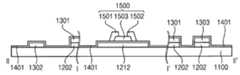
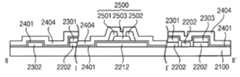
도 7은 본 발명의 다른 실시예에 따른 터치 표시장치의 단면도이다. 도 8a 내지 8e는 도 7의 터치 표시 장치의 제조방법을 설명하기 위한 단면도들이다.7 is a cross-sectional view of a touch display device according to another embodiment of the present invention. 8A to 8E are cross-sectional views illustrating a method of manufacturing the touch display device of FIG.
도 7을 참조하면, 본 발명의 일 실시예에 따른 터치 표시 장치는 베이스 기판(1100), 배선 연결부(1202), 게이트 금속 패턴(1300), 제1 절연층(1401), 센싱 소자(1500), 제2 절연층(1404), 제2 게이트 전극(1610) 및 연결 전극(1620)을 포함한다. 상기 게이트 금속 패턴(1300)은 게이트 라인(1301), 공통전압배선(1302) 및 패드부(1303)를 포함한다.7, a touch display device according to an embodiment of the present invention includes a
상기 베이스 기판(1100) 상에 상기 배선 연결부(1202)가 형성된다. 상기 배선 연결부(1202)는 상기 게이트 라인(1301) 및 상기 패드부(1303) 사이의 전위차를 제거하는 역할을 한다. 상기 배선 연결부(1202)는 밴드 패스 필터(Band Pass Filter : BPF) 물질을 포함할 수 있다.The
상기 배선 연결부(1202)는 처음에 상기 게이트 라인(1301)의 하부, 상기 패드부(1303)의 하부 및 상기 게이트 라인(1301) 및 상기 패드부(1303) 사이를 연결하도록 형성된다. 그러나 본 발명의 일 실시예에 따른 터치 표시 장치의 제조 공정에서, 제2 절연층(1404)을 식각하는 과정에서 상기 게이트 라인(1301) 및 상기 패드부(1303) 사이를 연결하도록 형성된 배선 연결부(1202)는 동시에 식각된다. 따라서, 완성된 본 발명의 일 실시예에 따른 터치 표시 장치에서는 일부가 제거되어 완성된 터치 표시 장치의 상기 베이스 기판(1100) 상에는 상기 게이트 라인(1301) 및 상기 패드부(1303)의 하부에만 존재한다.The
상기 배선 연결부(1202)가 형성된 상기 베이스 기판(1100) 상에 게이트 금속 패턴(1300)이 형성된다. 상기 게이트 금속 패턴(1300)은 게이트 라인(1301), 공통전압배선(1302) 및 패드부(1303)를 포함한다. 상기 게이트 라인(1301)은 복수 개가 배치되며, 제1 방향(D1)으로 연장된다. 상기 게이트 라인(1301)의 좌측에는 상기 공통전압배선(1302)이 배치된다. 상기 공통전압배선(1302)은 상기 게이트 라인(1301)이 연장되는 제1 방향(D1)과 수직인 제2 방향(D2)으로 연장된다. 상기 게이트 라인(1301)의 우측에는 상기 패드부(1303)가 배치된다. 상기 게이트 라인(1301) 및 상기 패드부(1303)는 연결 전극(1620)이 형성되기 전에는 서로 분리되어 있으며, 상기 게이트 라인(1301) 및 상기 패드부(1303) 사이의 전위차로 인하여 정전기가 발생하게 된다. 상기 정전기는 센서 구동시 표시장치의 가로줄을 발생시키며, 이로 인해 표시장치의 표시 품질이 저하되므로, 상기 연결 전극(1620)이 상기 게이트 라인(1301) 및 상기 패드부(1303)를 연결하기 전까지 과정에서 전위차를 제거하기 위해 상기 배선 연결부(1202)가 이용된다.A gate metal pattern 1300 is formed on the
상기 게이트 금속 패턴 형성된 베이스 기판(1100) 상에는 제1 절연층(1401)이 형성된다. 상기 제1 절연층(1401)이 형성된 베이스 기판(1100) 상에는 상기 센싱 소자(1500)가 형성된다. 상기 센싱 소자(1500)는 제2 소스 전극(1501), 제2 드레인 전극(1502) 및 제2 반도체 패턴(1503)을 포함한다.A first insulating
상기 센싱 소자(1500)가 형성된 베이스 기판(1100) 상에 제2 절연층(1404)이 형성된다. 상기 제2 절연층(1404)이 형성된 베이스 기판(1100) 상에는 제2 게이트 전극(1610) 및 연결 전극(1620)이 형성된다. 상기 제2 게이트 전극(1610) 및 연결 전극(1620)은 동일한 층에 형성된다. 상기 연결전극(1620)은 상기 게이트 라인(1301)과 상기 패드부(1303)를 연결한다.A second insulating
도 8a를 참조하면, 상기 베이스 기판(1100) 상에 반도체 층(1200)이형성된다. 상기 반도체 층(1200) 배선 연결부(1202) 및 제2 반도체 차광 패턴(1212)을 포함한다. 상기 배선 연결부(1202)는 상기 게이트 라인(1301)이 형성되는 위치 및 상기 패드부(1303)가 형성되는 위치에 형성되며, 상기 게이트 라인(1301)과 상기 패드부(1303) 사이를 연결하도록 형성된다.Referring to FIG. 8A, a semiconductor layer 1200 is formed on the
상기 제2 반도체 차광 패턴(1212)은 센싱 소자(1500)가 형성되는 영역에 형성된다. 상기 제2 반도체 차광 패턴(1212)은 밴드패스필터 물질을 포함하여, 가시광은 차단하고 적외선 광은 투과시킬 수 있다.The second semiconductor
도 8b를 참조하면, 상기 배선 연결부(1202)가 형성된 베이스 기판(1100) 상에 상기 게이트 금속 패턴(1300)이 형성된다. 상기 게이트 금속 패턴(1300)은 상기 게이트 라인(1301), 상기 공통전압배선(1302) 및 상기 패드부(1303)를 포함한다.Referring to FIG. 8B, the gate metal pattern 1300 is formed on a
상기 게이트 라인(1301) 및 상기 패드부(1303)는 상기 배선 연결부(1202)와 중첩되도록 배치된다. 상기 공통전압배선(1302)은 상기 배선 연결부(1202)와 중첩되지 않는다. 상기 배선 연결부(1202)는 낮은 저항값을 갖는 밴드 패스 필터 물질로 구성되므로, 상기 게이트 라인(1301) 및 상기 패드부(1303)를 연결하여 등전위를 갖도록 한다. 따라서, 정전기 발생으로 불량이 발생하는 상기 게이트 라인(1301) 및 상기 패드부(1303) 사이가 서로 등전위를 가지게 되어 정전기가 발생되지 않도록 하는 역할을 한다.The
도 8c를 참조하면, 상기 게이트 금속 패턴(1300)이 형성된 베이스 기판(1100) 상에 제1 절연층(1401) 및 센싱 소자(1500)가 순차적으로 형성된다. 상기 제1 절연층(1401)이 형성된 후 상기 제2 반도체 차광 패턴(1212)이 형성된 영역에 상기 센싱 소자(1500)가 형성된다. 상기 센싱 소자(1500)를 형성하는 과정은 건식 식각으로 진행된다. 이 과정에서 정전기가 발생될 수 있으며, 상기 게이트 라인(1301) 및 상기 패드부(1303) 사이의 전위차로 인해 정전기가 발생된다. 그러나 본 발명의 일 실시예에 따른 터치 표시장치에서는 상기 배선 연결부(1202)에 의해 상기 게이트 라인(1301) 및 상기 패드부(1303) 사이가 서로 등전위를 가지게 되어 정전기 발생을 방지할 수 있다.Referring to FIG. 8C, a first insulating
도 8d를 참조하면, 상기 센싱 소자(1500)가 형성된 베이스 기판(1100) 상에 제2 절연층(1404)이 형성된다. 상기 제2 절연층(1404)은 상기 센싱 소자(1500)와 제2 게이트 전극(1610)을 절연시킨다. 도8d는 상기 제2 절연층(1404)이 식각되기 전의 상태를 나타낸다. 이후 상기 제2 절연층(1404)이 식각되며, 상기 게이트 라인(1301)과 상기 패드부(1303) 사이를 연결하는 상기 배선 연결부(1202)가 동시에 식각된다.Referring to FIG. 8D, a second insulating
도 8e를 참조하면, 상기 제2 절연층(1404)이 형성된 후에, 상기 제2 절연층(1404)을 식각한 상태가 나타난다. 상기 제2 절연층(1404)을 식각하는 과정에서 상기 게이트 라인(1301)과 상기 패드부(1303) 사이를 연결하는 상기 배선 연결부(1202)가 동시에 식각된다. 따라서, 상기 배선 연결부(1202)는 일부가 제거되어 상기 게이트 라인(1301)의 하부 및 상기 패드부(1303)의 하부에 남겨진다. 즉, 상기 제2 절연층(1404)을 식각하는 과정에서 상기 배선 연결부(1202)의 일부가 제거되어 상기 베이스 기판(1100) 상에 상기 배선 연결부(1202)의 일부가 남겨지고, 상기 게이트 라인(1301), 상기 공통전압배선(1302), 상기 패드부(1303) 및 센싱 소자(1500)가 형성된 상태가 나타난다. 이 때, 연결 전극(1620)에 의해 연결되기 위한 상기 게이트 라인(1301)의 일부 및 상기 패드부(1303)의 일부가 노출된다.Referring to FIG. 8E, after the second insulating
다시 도 7을 참조하면, 상기 제2 절연층(1404)을 식각하는 과정에서 상기 배선 연결부(1202)의 일부가 제거되고, 상기 베이스 기판(1100) 상에 제2 게이트 전극(1610) 및 연결 전극(1620)이 형성된다. 상기 제2 게이트 전극(1610) 및 연결 전극(1620)은 동일한 층에 형성된다. 상기 연결 전극(1620)은 일부가 노출된 상기 게이트 라인(1301) 및 상기 패드부(1303)를 연결하는 역할을 한다. 상기 연결 전극(1620)이 분리되어 있는 상기 게이트 라인(1301) 및 상기 패드부(1303)를 연결하기 전에는 상기 게이트 라인(1301)과 상기 패드부(1303) 사이에 전위차가 존재하여 정전기가 발생할 수 있다. 그러나, 상기 배선 연결부(1202)가 상기 연결 전극(1620)이 상기 게이트 라인(1301) 및 상기 패드부(1303)를 연결하기 전까지 전위차를 제거하는 역할을 하게 되므로 정전기 발생이 방지된다. 본 실시예에서는 상기 배선 연결부(1202)가 상기 게이트 라인(1301)과 중첩되는 것을 예를 들어 설명하였으나, 이에 한정되지 않고 상기 배선 연결부(1202)는 상기 게이트 라인(1301) 및 바이어스 전압라인을 포함하는 신호 라인들과 중첩될 수 있다.7, a part of the
본 실시예에서는 밴드 패스 필터 물질을 포함하는 상기 배선 연결부(1202)가 끊어진 금속 패턴의 양끝을 연결하여 전위차를 제거한다. 따라서, 끊어진 금속 패턴의 양끝이 서로 등전위를 가지게 되어 정전기가 방지된다. 또한 상기 배선 연결부(1202)는 밴드 패스 필터 물질을 이용하므로 식각 공정에서 용이하게 제거할 수 있어 불량을 방지할 수 있다.In the present embodiment, the
도 9는 본 발명의 또 다른 실시예에 따른 터치 표시장치의 단면도이다. 도 10a 내지 10e는 도 9의 터치 표시 장치의 제조방법을 설명하기 위한 단면도들이다.9 is a cross-sectional view of a touch display device according to another embodiment of the present invention. 10A to 10E are cross-sectional views for explaining the manufacturing method of the touch display device of FIG.
도 9를 참조하면, 본 발명의 일 실시예에 따른 터치 표시 장치는 베이스 기판(2100), 배선 연결부(2202), 게이트 금속 패턴(2300), 제1 절연층(2401), 센싱 소자(2500), 제2 절연층(2404), 제2 게이트 전극(2610) 및 연결 전극(2620)을 포함한다. 상기 게이트 금속 패턴(2300)은 게이트 라인(2301), 공통전압배선(2302) 및 패드부(2303)를 포함한다.9, a touch display device according to an embodiment of the present invention includes a
상기 베이스 기판(2100) 상에 상기 배선 연결부(2202)가 형성된다. 상기 배선 연결부(2202)는 상기 게이트 라인(2301) 및 상기 패드부(2303) 사이의 전위차를 제거하는 역할을 한다. 상기 배선 연결부(2202)는 밴드 패스 필터(Band Pass Filter : BPF) 물질을 포함할 수 있다.The
상기 배선 연결부(2202)는 처음에 상기 게이트 라인(2301)의 하부 및 상기 패드부(2303)의 하부에 형성되며, 상기 게이트 라인(2301) 및 상기 패드부(2303) 사이를 연결하도록 형성된 도 8a 내지 도 8e에 도시된 실시예와는 달리 상기 게이트 라인(2301) 및 상기 패드부(2303) 사이에 상기 게이트 라인(2301) 및 상기 패드부(2303)와 분리되어 형성된다. 그러나 본 발명의 일 실시예에 따른 터치 표시 장치의 제조 공정에서, 제2 절연층(2404)을 식각하는 과정에서 상기 게이트 라인(2301) 및 상기 패드부(2303) 사이에 상기 게이트 라인(2301) 및 상기 패드부(2303)와 분리되어 형성된 상기 배선 연결부(2202)는 동시에 식각된다. 따라서, 완성된 본 발명의 일 실시예에 따른 터치 표시 장치에서 상기 배선 연결부(2202)는 일부가 제거되어 완성된 터치 표시 장치의 상기 베이스 기판(2100) 상에는 상기 게이트 라인(2301)의 하부 및 상기 패드부(2303)의 하부에만 존재한다.The
상기 배선 연결부(2202)가 형성된 상기 베이스 기판(2100) 상에 게이트 금속 패턴(2300)이 형성된다. 상기 게이트 금속 패턴(2300)은 게이트 라인(2301), 공통전압배선(2302) 및 패드부(2303)를 포함한다. 상기 게이트 라인(2301)은 복수 개가 배치되며, 제1 방향(D1)으로 연장된다. 상기 게이트 라인(2301)의 좌측에는 상기 공통전압배선(2302)이 배치된다. 상기 공통전압배선(2302)은 상기 게이트 라인(2301)이 연장되는 제1 방향(D1)과 수직인 제2 방향(D2)으로 연장된다. 상기 게이트 라인(2301)의 우측에는 상기 패드부(2303)가 배치된다. 상기 게이트 라인(2301) 및 상기 패드부(2303)는 연결 전극(2620)이 형성되기 전에는 서로 분리되어 있으며, 상기 게이트 라인(2301) 및 상기 패드부(2303) 사이의 전위차로 인하여 정전기가 발생하게 된다. 상기 정전기는 센서 구동시 표시장치의 가로줄을 발생시키며, 이로 인해 표시장치의 표시 품질이 저하되므로, 상기 연결 전극(2620)이 상기 게이트 라인(2301) 및 상기 패드부(2303)를 연결하기 전까지 과정에서 전위차를 제거하기 위해 상기 배선 연결부(2202)가 이용된다.A gate metal pattern 2300 is formed on the
상기 게이트 금속 패턴 형성된 베이스 기판(2100) 상에는 제1 절연층(2401)이 형성된다. 상기 제1 절연층(2401)은 상기 게이트 라인(2301)의 상부에 형성된다.A first insulating
상기 제1 절연층(2401)이 형성된 베이스 기판(2100) 상에는 상기 센싱 소자(2500)가 형성된다. 상기 센싱 소자(2500)는 제2 소스 전극(2501), 제2 드레인 전극(2502) 및 제2 반도체 패턴(2503)을 포함한다.The
상기 센싱 소자(2500)가 형성된 베이스 기판(2100) 상에 제2 절연층(2404)이 형성된다. 상기 제2 절연층(2404)이 형성된 베이스 기판(2100) 상에는 제2 게이트 전극(2620) 및 연결 전극(2620)이 형성된다. 상기 연결 전극(2620)은 상기 게이트 라인(2301)과 상기 패드부(2303)를 연결한다.A second insulating
도 10a를 참조하면, 상기 베이스 기판(2100) 상에 반도체 층(2200)이형성된다. 상기 반도체 층(2200) 배선 연결부(2202) 및 제2 반도체 차광 패턴(2212)을 포함한다. 상기 배선 연결부(2202)는 상기 게이트 라인(2301)이 형성되는 위치 및 상기 패드부(2303)가 형성되는 위치에 형성되며, 상기 게이트 라인(2301) 및 상기 패드부(2303) 사이를 연결하도록 형성된 도 8a 내지 도 8e에 도시된 실시예와는 달리 상기 게이트 라인(2301) 및 상기 패드부(2303) 사이에 상기 게이트 라인(2301) 및 상기 패드부(2303)와 분리되어 형성된다.Referring to FIG. 10A, a semiconductor layer 2200 is formed on the
상기 제2 반도체 차광 패턴(2212)은 센싱 소자(2500)가 형성되는 영역에 형성된다. 상기 제2 반도체 차광 패턴(2212)은 밴드패스필터 물질을 포함하여, 가시광은 차단하고 적외선 광은 투과시킬 수 있다.The second semiconductor
도 10b를 참조하면, 상기 배선 연결부(2202)가 형성된 베이스 기판(2100) 상에 상기 게이트 금속 패턴(2300)이 형성된다. 상기 게이트 금속 패턴(2300)은 상기 게이트 라인(2301), 상기 공통전압배선(2302) 및 상기 패드부(2303)를 포함한다. 상기 게이트 라인(2301) 및 상기 패드부(2303)는 상기 배선 연결부(2202)와 중첩되도록 배치된다. 상기공통전압배선(2302)은 상기 배선 연결부(2202)와 중첩되지 않는다. 상기 배선 연결부(2202)는 낮은 저항값을 갖는 밴드 패스 필터 물질로 구성되므로, 상기 게이트 라인(2301) 및 상기 패드부(2303) 사이에 상기 게이트 라인(2301) 및 상기 패드부(2303)과 분리되어 형성된 상기 배선 연결부(2202)가 플로팅 게이트로서 버퍼 역할을 수행한다. 따라서, 정전기 발생으로 불량이 발생하는 상기 게이트 라인(2301) 및 상기 패드부(2303) 사이에서 정전기가 발생되지 않도록 한다.Referring to FIG. 10B, the gate metal pattern 2300 is formed on a
도 10c를 참조하면, 상기 게이트 금속 패턴(2300)이 형성된 베이스 기판(2100) 상에 제1 절연층(2401) 및 센싱 소자(2500)가 순차적으로 형성된다. 상기 제1 절연층(2401)이 형성된 후 상기 제2 반도체 차광 패턴(2212)이 형성된 영역에 상기 센싱 소자(2500)가 형성된다. 상기 센싱 소자(2500)를 형성하는 과정은 건식 식각으로 진행된다. 이 과정에서 정전기가 발생될 수 있으며, 상기 게이트 라인(2301) 및 상기 패드부(2303) 사이의 전위차로 인해 정전기가 발생된다. 그러나 본 발명의 일 실시예에 따른 터치 표시장치에서는 상기 게이트 라인(2301) 및 상기 패드부(2303)와 분리되어 형성된 상기 배선 연결부(2202)가 플로팅 게이트로서 버퍼 역할을 수행하므로 정전기 발생을 방지할 수 있다.Referring to FIG. 10C, a first insulating
도 10d를 참조하면, 상기 센싱 소자(2500)가 형성된 베이스 기판(2100) 상에 제2 절연층(2404)이 형성된다. 상기 제2 절연층(2404)은 상기 센싱 소자(2500)와 제2 게이트 전극(2610)을 절연시킨다. 도10d는 상기 제2 절연층(2404)이 식각되기 전의 상태를 나타낸다. 이후 상기 제2 절연층(2404)이 식각되며, 상기 게이트 라인(2301) 및 상기 패드부(2303)와 분리되어 형성된 상기 배선 연결부(2202)가 동시에 식각된다.Referring to FIG. 10D, a second insulating
도 10e를 참조하면, 상기 제2 절연층(2404)이 형성된 후에, 상기 제2 절연층(2404)을 식각한 상태가 나타난다. 상기 제2 절연층(1404)을 식각하는 과정에서 상기 게이트 라인(2301) 및 상기 패드부(2303)와 분리되어 형성된 상기 배선 연결부(2202)가 동시에 식각된다. 따라서, 상기 배선 연결부(2202)는 일부가 제거되어 상기 게이트 라인(2301)의 하부 및 상기 패드부(2303)의 하부에 남겨진다. 즉, 상기 제2 절연층(2404)을 식각하는 과정에서 상기 배선 연결부(2202)의 일부가 제거되어 상기 베이스 기판(2100) 상에 상기 배선 연결부(2202)의 일부가 남겨지고, 상기 게이트 라인(2301), 상기 공통전압배선(2302), 상기 패드부(2303) 및 센싱 소자(2500)가 형성된 상태가 나타난다. 이 때, 상기 연결 전극(2620)에 의해 연결되기 위한 상기 게이트 라인(2301)의 일부 및 상기 패드부(2303)의 일부가 노출된다.Referring to FIG. 10E, after the second insulating
다시 도 9를 참조하면, 상기 제2 절연층(2404)을 식각하는 과정에서 상기 배선 연결부(2202)의 일부가 제거되고, 상기 베이스 기판(2100) 상에 제2 게이트 전극(2610) 및 연결 전극(2620)이 형성된다. 상기 연결 전극(2620)은 일부가 노출된 상기 게이트 라인(2301) 및 상기 패드부(2303)를 연결하는 역할을 한다. 상기 연결 전극(2620)이 분리되어 있는 상기 게이트 라인(2301) 및 상기 패드부(2303)를 연결하기 전에는 상기 게이트 라인(2301)과 상기 패드부(2303) 사이에 전위차가 존재하여 정전기가 발생할 수 있다. 그러나, 상기 배선 연결부(2202)가 상기 연결 전극(2620)이 상기 게이트 라인(2301) 및 상기 패드부(2303)를 연결하기 전까지 전위차를 줄여주는 버퍼 역할을 하게 되므로 정전기 발생이 방지된다. 본 실시예에서는 상기 배선 연결부(2202)가 상기 게이트 라인(2301)과 중첩되는 것을 예를 들어 설명하였으나, 이에 한정되지 않고 상기 배선 연결부(2202)는 상기 게이트 라인(2301) 및 바이어스 전압라인을 포함하는 신호 라인들과 중첩될 수 있다.9, a part of the
본 실시예에서는 밴드 패스 필터 물질을 포함하는 상기 배선 연결부(2202)가 끊어진 금속 패턴의 양끝 사이에서 플로팅 게이트로서 버퍼 역할을 한다. 따라서, 끊어진 금속 패턴의 양끝 사이에서 발생되는 정전기가 방지된다. 또한 상기 배선 연결부(2202)는 밴드 패스 필터 물질을 이용하므로 식각 공정에서 용이하게 제거할 수 있어 불량을 방지할 수 있다.In the present embodiment, the
이상에서 설명한 바와 같이, 본 발명의 터치 표시 장치 및 이를 이용하는 터치 표시 장치의 제조방법에 따르면, 표시 장치에서 발생되는 정전기를 방지하여 표시 품질을 향상시킬 수 있다.As described above, according to the touch display device of the present invention and the manufacturing method of the touch display device using the same, it is possible to prevent the static electricity generated in the display device and improve the display quality.
이상에서는 본 발명의 바람직한 실시예들을 참조하여 설명하였지만, 해당 기술분야의 숙련된 당업자 또는 해당 기술분야에 통상의 지식을 갖는 자라면 후술될 특허청구범위에 기재된 본 발명의 사상 및 기술 영역으로부터 벗어나지 않는 범위 내에서 본 발명을 다양하게 수정 및 변경시킬 수 있음을 이해할 수 있을 것이다.While the present invention has been described with reference to exemplary embodiments, it is to be understood that the invention is not limited to the disclosed exemplary embodiments, but, on the contrary, is intended to cover various modifications and equivalent arrangements included within the spirit and scope of the appended claims. It will be understood that various modifications and changes may be made thereto without departing from the scope of the present invention.
100, 1100, 2100: 베이스 기판201: 가드링
202: 배선 연결부300: 금속 패턴
301: 게이트 라인302: 공통전압배선
303: 패드부401: 제1 절연층
404: 제2 절연층500: 센싱 소자
501: 제2 소스 전극502: 제2 드레인 전극
503: 제2 반도체 패턴610: 제2 게이트 전극
620 : 연결 전극100, 1100, 2100: base substrate 201: guard ring
202: wiring connection part 300: metal pattern
301: gate line 302: common voltage wiring
303: pad portion 401: first insulating layer
404: second insulation layer 500: sensing element
501: second source electrode 502: second drain electrode
503: second semiconductor pattern 610: second gate electrode
620: connecting electrode
Claims (20)
Translated fromKorean상기 베이스 기판 위에 배치되고, 가시광은 차단하고 적외선 광을 투과하는 반도체 차광패턴;
상기 반도체 차광패턴 위에 배치되며, 입사되는 적외선 광에 대응하여 위치를 검출하는 센싱 소자;
상기 센싱 소자를 구동하기 위한 구동 소자;
상기 센싱 소자 또는 상기 구동 소자와 전기적으로 연결되며 일 방향으로 연장되는 신호 라인; 및
상기 반도체 차광 패턴과 동일한 물질을 포함하며, 상기 신호 라인의 아래에 배치되는 배선 연결부를 포함하는 터치 표시 장치.A base substrate;
A semiconductor light shielding pattern disposed on the base substrate and shielding visible light and transmitting infrared light;
A sensing element disposed on the semiconductor light shielding pattern and detecting a position corresponding to incident infrared light;
A driving element for driving the sensing element;
A signal line electrically connected to the sensing element or the driving element and extending in one direction; And
And a wiring connection portion including the same material as the semiconductor light shielding pattern and disposed under the signal line.
상기 반도체 차광패턴 위에 배치된 반도체 패턴;
상기 반도체 패턴의 일단과 중첩하는 소스 전극;
상기 소스 전극과 이격되며, 상기 반도체 패턴의 타단과 중첩하는 드레인 전극; 및
상기 소스 전극 및 드레인 전극 위에 배치된 게이트 전극을 포함하는 것을 특징으로 하는 터치 표시장치.2. The method of claim 1, wherein the sensing element
A semiconductor pattern disposed on the semiconductor light shielding pattern;
A source electrode overlapping one end of the semiconductor pattern;
A drain electrode spaced apart from the source electrode and overlapping with the other end of the semiconductor pattern; And
And a gate electrode disposed on the source electrode and the drain electrode.
상기 배선 연결부 위에 배치되어 일 방향으로 연장되는 신호 라인을 포함하는 금속 패턴을 형성하는 단계; 및
상기 금속 패턴이 형성된 베이스 기판 상에, 입사되는 적외선 광에 대응하여 위치를 검출하기 위한 센싱 소자를 형성하는 단계를 포함하는 터치 표시 장치의 제조방법.A semiconductor light shielding pattern for shielding visible light and transmitting infrared light on the base substrate; a wiring connection portion disposed on the display region, the wiring connection portion including the same material as the semiconductor light shielding pattern; Forming a semiconductor layer including a guard ring connected to the wiring connection portion;
Forming a metal pattern on the wiring connection portion and including signal lines extending in one direction; And
And forming a sensing element on the base substrate on which the metal pattern is formed to detect a position corresponding to incident infrared light.
상기 반도체 차광 패턴이 형성된 베이스 기판 상에 반도체 패턴을 형성하는 단계;
상기 반도체 패턴이 형성된 베이스 기판 상에 소스 전극 및 드레인 전극을 형성하는 단계;
상기 소스 전극 및 드레인 전극이 형성된 베이스 기판 상에 절연층을 형성하는 단계; 및
상기 절연층이 형성된 베이스 기판 상에 게이트 전극을 형성하는 단계를 포함하는 것을 특징으로 하는 터치 표시 장치의 제조방법.7. The method of claim 6, wherein forming the sensing element
Forming a semiconductor pattern on the base substrate on which the semiconductor light shielding pattern is formed;
Forming a source electrode and a drain electrode on the base substrate on which the semiconductor pattern is formed;
Forming an insulating layer on the base substrate on which the source electrode and the drain electrode are formed; And
And forming a gate electrode on the base substrate on which the insulating layer is formed.
상기 주변 영역 상에 배치되며, 상기 신호 라인과 교차하는 방향으로 연장되는 공통전압배선; 및
상기 주변 영역 상에 배치되며, 상기 신호 라인 및 상기 배선 연결부와 이격되는 패드부를 포함하는 것을 특징으로 하는 터치 표시 장치의 제조방법.7. The semiconductor device according to claim 6,
A common voltage line disposed on the peripheral region and extending in a direction crossing the signal line; And
And a pad portion disposed on the peripheral region and spaced apart from the signal line and the wiring connection portion.
상기 배선 연결부 위에 배치되어 일 방향으로 연장되는 신호 라인을 포함하는 금속 패턴을 형성하는 단계; 및
상기 금속 패턴이 형성된 베이스 기판 상에, 입사되는 적외선 광에 대응하여 위치를 검출하기 위한 센싱 소자를 형성하는 단계를 포함하는 터치 표시 장치의 제조방법.Forming a semiconductor layer on the base substrate, the semiconductor layer including a semiconductor light-shielding pattern that shields visible light and transmits infrared light, and a wiring connection portion that includes the same material as the semiconductor light-shielding pattern and is disposed in the display region;
Forming a metal pattern on the wiring connection portion and including signal lines extending in one direction; And
And forming a sensing element on the base substrate on which the metal pattern is formed to detect a position corresponding to incident infrared light.
상기 반도체 차광 패턴이 형성된 베이스 기판 상에 반도체 패턴을 형성하는 단계;
상기 반도체 패턴이 형성된 베이스 기판 상에 소스 전극 및 드레인 전극을 형성하는 단계;
상기 소스 전극 및 드레인 전극이 형성된 베이스 기판 상에 절연층을 형성하는 단계; 및
상기 절연층이 형성된 베이스 기판 상에 게이트 전극을 형성하는 단계를 포함하는 것을 특징으로 하는 터치 표시 장치의 제조방법.14. The method of claim 13, wherein forming the sensing element comprises:
Forming a semiconductor pattern on the base substrate on which the semiconductor light shielding pattern is formed;
Forming a source electrode and a drain electrode on the base substrate on which the semiconductor pattern is formed;
Forming an insulating layer on the base substrate on which the source electrode and the drain electrode are formed; And
And forming a gate electrode on the base substrate on which the insulating layer is formed.
상기 주변 영역 상에 배치되며, 상기 신호 라인과 교차하는 방향으로 연장되는 공통전압배선; 및
상기 주변 영역 상에 배치되며, 상기 신호 라인 및 상기 배선 연결부와 이격되는 및 패드부를 포함하는 것을 특징으로 하는 터치 표시 장치의 제조방법.14. The method of claim 13, wherein the metal pattern
A common voltage line disposed on the peripheral region and extending in a direction crossing the signal line; And
And a pad portion disposed on the peripheral region and spaced apart from the signal line and the wiring connection portion.
14. The method of claim 13, wherein the wiring connection part is formed separately from the signal line and the pad part in a region between the signal line and the pad part.
Priority Applications (2)
| Application Number | Priority Date | Filing Date | Title |
|---|---|---|---|
| KR1020130022707AKR20140110137A (en) | 2013-03-04 | 2013-03-04 | Touch display apparatus and method of manufacturing the same |
| US14/065,686US9389452B2 (en) | 2013-03-04 | 2013-10-29 | Electrostatic member in forming touch display apparatus and method of manufacturing the same |
Applications Claiming Priority (1)
| Application Number | Priority Date | Filing Date | Title |
|---|---|---|---|
| KR1020130022707AKR20140110137A (en) | 2013-03-04 | 2013-03-04 | Touch display apparatus and method of manufacturing the same |
Publications (1)
| Publication Number | Publication Date |
|---|---|
| KR20140110137Atrue KR20140110137A (en) | 2014-09-17 |
Family
ID=51420804
Family Applications (1)
| Application Number | Title | Priority Date | Filing Date |
|---|---|---|---|
| KR1020130022707AWithdrawnKR20140110137A (en) | 2013-03-04 | 2013-03-04 | Touch display apparatus and method of manufacturing the same |
Country Status (2)
| Country | Link |
|---|---|
| US (1) | US9389452B2 (en) |
| KR (1) | KR20140110137A (en) |
Families Citing this family (7)
| Publication number | Priority date | Publication date | Assignee | Title |
|---|---|---|---|---|
| CN104267856B (en) | 2014-09-29 | 2016-08-17 | 合肥鑫晟光电科技有限公司 | A kind of touch-control display panel and display device |
| KR102291466B1 (en) | 2015-01-20 | 2021-08-19 | 삼성디스플레이 주식회사 | Touch screen panel |
| KR102640164B1 (en)* | 2016-05-09 | 2024-02-23 | 삼성디스플레이 주식회사 | Thin film transistor array panel |
| JP6873753B2 (en)* | 2017-03-09 | 2021-05-19 | パナソニック液晶ディスプレイ株式会社 | Liquid crystal display device |
| CN109407883B (en)* | 2018-09-27 | 2022-04-26 | 合肥鑫晟光电科技有限公司 | Touch screen, manufacturing method thereof and display device |
| US10727284B2 (en)* | 2018-11-15 | 2020-07-28 | Wuhan China Star Optoelectronics Semiconductor Display Technology Co., Ltd. | Method of fabricating organic light-emitting diode touch display screen |
| US11520444B2 (en)* | 2020-04-21 | 2022-12-06 | Samsung Display Co., Ltd. | Display device and method of inspecting the same |
Family Cites Families (15)
| Publication number | Priority date | Publication date | Assignee | Title |
|---|---|---|---|---|
| JPH08243084A (en) | 1995-03-09 | 1996-09-24 | Seiko Epson Corp | Portable electronic devices |
| KR100249166B1 (en) | 1997-03-07 | 2000-03-15 | 김영환 | Esd protection circuit and manufacturing method thereof |
| GB2407207B (en) | 2003-10-13 | 2006-06-07 | Micron Technology Inc | Structure and method for forming a capacitively coupled chip-to-chip signalling interface |
| KR100999082B1 (en) | 2003-10-21 | 2010-12-07 | 삼성전자주식회사 | Thin Film Transistor Board |
| KR20080011855A (en) | 2006-08-01 | 2008-02-11 | 삼성전자주식회사 | Manufacturing Method of Display Cells and Display Cells |
| KR20080018720A (en) | 2006-08-25 | 2008-02-28 | 삼성전자주식회사 | Thin film transistor array panel |
| KR20080046891A (en) | 2006-11-23 | 2008-05-28 | 삼성전자주식회사 | Manufacturing method of liquid crystal display device |
| US20080204618A1 (en) | 2007-02-22 | 2008-08-28 | Min-Kyung Jung | Display substrate, method for manufacturing the same, and display apparatus having the same |
| US8232625B2 (en) | 2009-03-26 | 2012-07-31 | International Business Machines Corporation | ESD network circuit with a through wafer via structure and a method of manufacture |
| KR101073333B1 (en) | 2009-08-27 | 2011-10-12 | 삼성모바일디스플레이주식회사 | Touch Screen Panel and fabrication method thereof |
| US20120326973A1 (en)* | 2010-03-01 | 2012-12-27 | Sharp Kabushiki Kaisha | Display device |
| KR101718007B1 (en)* | 2010-08-13 | 2017-03-21 | 삼성디스플레이 주식회사 | Touch display panel and method of manufacturing the same |
| KR101726739B1 (en)* | 2010-12-21 | 2017-04-14 | 삼성디스플레이 주식회사 | Touch display substrate and touch display panel having the same |
| KR101770969B1 (en)* | 2011-01-21 | 2017-08-25 | 삼성디스플레이 주식회사 | Substrate of sensing touch and method of manufacturing the substrate |
| KR20130027188A (en)* | 2011-09-07 | 2013-03-15 | 삼성디스플레이 주식회사 | Display device and manufacturing method thereof |
- 2013
- 2013-03-04KRKR1020130022707Apatent/KR20140110137A/ennot_activeWithdrawn
- 2013-10-29USUS14/065,686patent/US9389452B2/ennot_activeExpired - Fee Related
Also Published As
| Publication number | Publication date |
|---|---|
| US20140247403A1 (en) | 2014-09-04 |
| US9389452B2 (en) | 2016-07-12 |
Similar Documents
| Publication | Publication Date | Title |
|---|---|---|
| US11714309B2 (en) | Display device | |
| KR20140110137A (en) | Touch display apparatus and method of manufacturing the same | |
| US12085823B2 (en) | Display device and semiconductor device | |
| US20110157039A1 (en) | Liquid crystal display device and method of fabricating the same | |
| KR101332048B1 (en) | Display device and method of manufacturing the same | |
| CN106873212A (en) | Backplane substrate including in-box touch panel, liquid crystal display device, and manufacturing method | |
| KR20150026033A (en) | Liquid crystal display device and method of fabricating the same | |
| CN103676375A (en) | Array substrate and manufacturing method thereof | |
| CN105093736A (en) | IPS array substrate, manufacture method thereof and display device | |
| US7995164B2 (en) | Array substrate having a particular light shielding portion in the non-display region | |
| US8502946B2 (en) | Array substrate of fringe field switching mode liquid crystal display panel and method of manufacturing the same | |
| KR20130061553A (en) | Display panel and fabrication method a display substrate for display panel | |
| KR101799938B1 (en) | Liquid crystal display device | |
| US20110169000A1 (en) | Display substrate and method of manufacturing the same | |
| TWI335483B (en) | Pixel structure and liquid crystal display panel | |
| CN103926761B (en) | A kind of test structure and its manufacturing method for array substrate | |
| US20110169004A1 (en) | Display device and manufacturing method therefor | |
| US8351015B2 (en) | Liquid crystal display panel and method for testing the same | |
| KR100686235B1 (en) | Substrate for Liquid Crystal Display | |
| KR101784445B1 (en) | Array substrate for Liquid crystal display device | |
| KR101327836B1 (en) | Liquid Crystal Display Device | |
| KR101441387B1 (en) | Liquid crystal display panel, manufacturing method thereof, and repair method using the same | |
| KR102048419B1 (en) | Liquid crystal display device | |
| KR101865704B1 (en) | Liquid crystal display device | |
| KR20080058036A (en) | Array substrate for liquid crystal display device and manufacturing method thereof |
Legal Events
| Date | Code | Title | Description |
|---|---|---|---|
| PA0109 | Patent application | Patent event code:PA01091R01D Comment text:Patent Application Patent event date:20130304 | |
| PG1501 | Laying open of application | ||
| PC1203 | Withdrawal of no request for examination | ||
| WITN | Application deemed withdrawn, e.g. because no request for examination was filed or no examination fee was paid |