KR20140108899A - Semiconductor device, and microprocessor, processor, system, data storage system and memory system including the semiconductor device - Google Patents
Semiconductor device, and microprocessor, processor, system, data storage system and memory system including the semiconductor deviceDownload PDFInfo
- Publication number
- KR20140108899A KR20140108899AKR1020130022761AKR20130022761AKR20140108899AKR 20140108899 AKR20140108899 AKR 20140108899AKR 1020130022761 AKR1020130022761 AKR 1020130022761AKR 20130022761 AKR20130022761 AKR 20130022761AKR 20140108899 AKR20140108899 AKR 20140108899A
- Authority
- KR
- South Korea
- Prior art keywords
- electrode
- memory
- semiconductor device
- variable resistance
- resistance element
- Prior art date
- Legal status (The legal status is an assumption and is not a legal conclusion. Google has not performed a legal analysis and makes no representation as to the accuracy of the status listed.)
- Granted
Links
Images


Classifications
- H—ELECTRICITY
- H10—SEMICONDUCTOR DEVICES; ELECTRIC SOLID-STATE DEVICES NOT OTHERWISE PROVIDED FOR
- H10N—ELECTRIC SOLID-STATE DEVICES NOT OTHERWISE PROVIDED FOR
- H10N70/00—Solid-state devices having no potential barriers, and specially adapted for rectifying, amplifying, oscillating or switching
- H10N70/20—Multistable switching devices, e.g. memristors
- G—PHYSICS
- G11—INFORMATION STORAGE
- G11C—STATIC STORES
- G11C13/00—Digital stores characterised by the use of storage elements not covered by groups G11C11/00, G11C23/00, or G11C25/00
- G11C13/0002—Digital stores characterised by the use of storage elements not covered by groups G11C11/00, G11C23/00, or G11C25/00 using resistive RAM [RRAM] elements
- G11C13/0004—Digital stores characterised by the use of storage elements not covered by groups G11C11/00, G11C23/00, or G11C25/00 using resistive RAM [RRAM] elements comprising amorphous/crystalline phase transition cells
- H—ELECTRICITY
- H10—SEMICONDUCTOR DEVICES; ELECTRIC SOLID-STATE DEVICES NOT OTHERWISE PROVIDED FOR
- H10N—ELECTRIC SOLID-STATE DEVICES NOT OTHERWISE PROVIDED FOR
- H10N70/00—Solid-state devices having no potential barriers, and specially adapted for rectifying, amplifying, oscillating or switching
- H10N70/801—Constructional details of multistable switching devices
- H10N70/821—Device geometry
- H10N70/826—Device geometry adapted for essentially vertical current flow, e.g. sandwich or pillar type devices
- H—ELECTRICITY
- H10—SEMICONDUCTOR DEVICES; ELECTRIC SOLID-STATE DEVICES NOT OTHERWISE PROVIDED FOR
- H10N—ELECTRIC SOLID-STATE DEVICES NOT OTHERWISE PROVIDED FOR
- H10N70/00—Solid-state devices having no potential barriers, and specially adapted for rectifying, amplifying, oscillating or switching
- H10N70/801—Constructional details of multistable switching devices
- H10N70/841—Electrodes
- H—ELECTRICITY
- H10—SEMICONDUCTOR DEVICES; ELECTRIC SOLID-STATE DEVICES NOT OTHERWISE PROVIDED FOR
- H10N—ELECTRIC SOLID-STATE DEVICES NOT OTHERWISE PROVIDED FOR
- H10N70/00—Solid-state devices having no potential barriers, and specially adapted for rectifying, amplifying, oscillating or switching
- H10N70/801—Constructional details of multistable switching devices
- H10N70/881—Switching materials
- H10N70/882—Compounds of sulfur, selenium or tellurium, e.g. chalcogenides
- H10N70/8828—Tellurides, e.g. GeSbTe
- H—ELECTRICITY
- H10—SEMICONDUCTOR DEVICES; ELECTRIC SOLID-STATE DEVICES NOT OTHERWISE PROVIDED FOR
- H10N—ELECTRIC SOLID-STATE DEVICES NOT OTHERWISE PROVIDED FOR
- H10N70/00—Solid-state devices having no potential barriers, and specially adapted for rectifying, amplifying, oscillating or switching
- H10N70/801—Constructional details of multistable switching devices
- H10N70/881—Switching materials
- H10N70/883—Oxides or nitrides
- H10N70/8833—Binary metal oxides, e.g. TaOx
- H—ELECTRICITY
- H10—SEMICONDUCTOR DEVICES; ELECTRIC SOLID-STATE DEVICES NOT OTHERWISE PROVIDED FOR
- H10N—ELECTRIC SOLID-STATE DEVICES NOT OTHERWISE PROVIDED FOR
- H10N70/00—Solid-state devices having no potential barriers, and specially adapted for rectifying, amplifying, oscillating or switching
- H10N70/801—Constructional details of multistable switching devices
- H10N70/881—Switching materials
- H10N70/883—Oxides or nitrides
- H10N70/8836—Complex metal oxides, e.g. perovskites, spinels
- G—PHYSICS
- G11—INFORMATION STORAGE
- G11C—STATIC STORES
- G11C2213/00—Indexing scheme relating to G11C13/00 for features not covered by this group
- G11C2213/50—Resistive cell structure aspects
- G11C2213/52—Structure characterized by the electrode material, shape, etc.
- H—ELECTRICITY
- H10—SEMICONDUCTOR DEVICES; ELECTRIC SOLID-STATE DEVICES NOT OTHERWISE PROVIDED FOR
- H10N—ELECTRIC SOLID-STATE DEVICES NOT OTHERWISE PROVIDED FOR
- H10N50/00—Galvanomagnetic devices
- H10N50/10—Magnetoresistive devices
Landscapes
- Chemical & Material Sciences (AREA)
- Crystallography & Structural Chemistry (AREA)
- Engineering & Computer Science (AREA)
- Materials Engineering (AREA)
- Semiconductor Memories (AREA)
- Hall/Mr Elements (AREA)
Abstract
Translated fromKoreanDescription
Translated fromKorean본 발명은 반도체 장치 및 이의 동작 방법에 관한 것으로, 더욱 상세하게는 가변 저항 소자를 포함하는 반도체 장치 및 이의 동작 방법에 관한 것이다.
The present invention relates to a semiconductor device and a method of operating the same, and more particularly, to a semiconductor device including a variable resistive element and a method of operating the same.
최근 전자기기의 소형화, 저전력화, 고성능화, 다양화 등에 따라 컴퓨터, 휴대용 통신기기 등 다양한 전자기기에서 정보를 저장할 수 있는 반도체 장치가 요구되고 있으며, 이에 대한 연구가 진행되고 있다. 이러한 반도체 장치로는 인가되는 전압 또는 전류에 따라 서로 다른 저항 상태 사이에서 스위칭하는 특성을 이용하여 데이터를 저장하는 반도체 장치, 예컨대 RRAM(Resistive Random Access Memory), PRAM(Phase-change Random Access Memory), FRAM(Ferroelectric Random Access Memory), MRAM(Magnetic Random Access Memory), 이-퓨즈(E-Fuse) 등이 있다.
2. Description of the Related Art In recent years, semiconductor devices capable of storing information in various electronic devices such as computers and portable communication devices have been demanded due to miniaturization, low power consumption, high performance, and diversification of electronic devices. Such a semiconductor device may be a semiconductor device such as a Resistive Random Access Memory (RRAM), a Phase-change Random Access Memory (PRAM), or the like, which stores data using characteristics of switching between different resistance states according to a voltage or current applied thereto. A ferroelectric random access memory (FRAM), a magnetic random access memory (MRAM), and an e-fuse.
본 발명의 일 실시예는, 가변 저항 소자에 인접하는 도전체를 통해 가변 저항 소자에 전기장을 인가하여 전류가 가변 저항 소자 내부에서 국부적인 영역으로 주입되도록 함으로써 가변 저항 소자의 스위칭 전류가 감소된 반도체 장치 및 이의 동작 방법을 제공한다.
According to an embodiment of the present invention, an electric field is applied to a variable resistance element through a conductor adjacent to the variable resistance element so that a current is injected into a local region within the variable resistance element, Device and method of operation thereof.
본 발명의 일 실시예에 따른 반도체 장치는, 제1 전극; 상기 제1 전극과 이격된 제2 전극; 상기 제1 전극과 상기 제2 전극 사이에 개재되는 가변 저항 소자; 및 상기 가변 저항 소자의 일측면 또는 타측면 중 어느 하나 이상에 배치되어 상기 가변 저항 소자에 이격된 채로 전기장을 인가하는 도전체를 포함할 수 있다.
A semiconductor device according to an embodiment of the present invention includes: a first electrode; A second electrode spaced apart from the first electrode; A variable resistance element interposed between the first electrode and the second electrode; And a conductor disposed on at least one side of the variable resistive element or on another side thereof for applying an electric field while being spaced apart from the variable resistive element.
본 발명의 일 실시예에 따른 마이크로프로세서는, 외부로부터 명령을 포함하는 신호를 수신받아 상기 명령의 추출이나 해독, 입력이나 출력의 제어를 수행하는 제어부; 상기 제어부가 명령을 해독한 결과에 따라서 연산을 수행하는 연산부; 및 상기 연산을 수행하는 데이터, 상기 연산을 수행한 결과에 대응하는 데이터 및 상기 연산을 수행하는 데이터의 주소 중 하나 이상을 저장하는 기억부를 포함하고, 상기 기억부는, 제1 전극; 상기 제1 전극과 이격된 제2 전극; 상기 제1 전극과 상기 제2 전극 사이에 개재되는 가변 저항 소자; 및 상기 가변 저항 소자의 일측면 또는 타측면 중 어느 하나 이상에 배치되어 상기 가변 저항 소자에 이격된 채로 전기장을 인가하는 도전체를 포함할 수 있다.
A microprocessor according to an embodiment of the present invention includes a control unit for receiving a signal including an instruction from the outside and controlling extraction or decoding of the instruction or input or output of the instruction; An operation unit for performing an operation according to a result of decoding the instruction by the control unit; And a storage unit for storing at least one of data for performing the operation, data corresponding to a result of performing the operation, and address of data for performing the operation, wherein the storage unit comprises: a first electrode; A second electrode spaced apart from the first electrode; A variable resistance element interposed between the first electrode and the second electrode; And a conductor disposed on at least one side of the variable resistive element or on another side thereof for applying an electric field while being spaced apart from the variable resistive element.
본 발명의 일 실시예에 따른 프로세서는, 외부로부터 입력된 명령에 따라 데이터를 이용하여 상기 명령에 대응하는 연산을 수행하는 코어부; 상기 연산을 수행하는 데이터, 상기 연산을 수행한 결과에 대응하는 데이터 및 상기 연산을 수행하는 데이터의 주소 중 하나 이상을 저장하는 캐시 메모리부; 및 상기 코어부와 상기 캐시 메모리부 사이에 연결되고, 상기 코어부와 상기 캐시 메모리부 사이에 데이터를 전송하는 버스 인터페이스를 포함하고, 상기 캐시 메모리부는, 제1 전극; 상기 제1 전극과 이격된 제2 전극; 상기 제1 전극과 상기 제2 전극 사이에 개재되는 가변 저항 소자; 및 상기 가변 저항 소자의 일측면 또는 타측면 중 어느 하나 이상에 배치되어 상기 가변 저항 소자에 이격된 채로 전기장을 인가하는 도전체를 포함할 수 있다.
A processor according to an embodiment of the present invention includes: a core unit for performing an operation corresponding to the instruction using data in accordance with an instruction input from the outside; A cache memory unit for storing at least one of data for performing the operation, data corresponding to a result of performing the operation, and address of data for performing the operation; And a bus interface connected between the core unit and the cache memory unit and transmitting data between the core unit and the cache memory unit, the cache memory unit comprising: a first electrode; A second electrode spaced apart from the first electrode; A variable resistance element interposed between the first electrode and the second electrode; And a conductor disposed on at least one side of the variable resistive element or on another side thereof for applying an electric field while being spaced apart from the variable resistive element.
본 발명의 일 실시예에 따른 시스템은, 외부로부터 입력된 명령을 해석하고 상기 명령을 해석한 결과에 따라 정보의 연산을 제어하는 프로세서; 상기 명령을 해석하기 위한 프로그램, 상기 정보를 저장하기 위한 보조기억장치; 상기 프로그램을 실행할 때 상기 프로세서가 상기 프로그램 및 상기 정보를 이용해 상기 연산을 수행할 수 있도록 상기 보조기억장치로부터 상기 프로그램 및 상기 정보를 이동시켜 저장하는 주기억장치; 및 상기 프로세서, 상기 보조기억장치 및 상기 주기억장치 중 하나 이상과 외부와의 통신을 수행하기 위한 인터페이스 장치를 포함하고, 상기 보조기억장치 및 상기 주기억장치 중 하나 이상은, 제1 전극; 상기 제1 전극과 이격된 제2 전극; 상기 제1 전극과 상기 제2 전극 사이에 개재되는 가변 저항 소자; 및 상기 가변 저항 소자의 일측면 또는 타측면 중 어느 하나 이상에 배치되어 상기 가변 저항 소자에 이격된 채로 전기장을 인가하는 도전체를 포함할 수 있다.
According to an embodiment of the present invention, there is provided a system including a processor for interpreting a command input from the outside and controlling an operation of information according to a result of analyzing the command; A program for interpreting the command, an auxiliary memory for storing the information; A main memory for moving and storing the program and the information from the auxiliary memory so that the processor can perform the calculation using the program and the information when the program is executed; And an interface device for performing communication with at least one of the processor, the auxiliary memory, and the main memory, and at least one of the auxiliary memory and the main memory includes: a first electrode; A second electrode spaced apart from the first electrode; A variable resistance element interposed between the first electrode and the second electrode; And a conductor disposed on at least one side of the variable resistive element or on another side thereof for applying an electric field while being spaced apart from the variable resistive element.
본 발명의 일 실시예에 따른 데이터 저장 시스템은, 데이터를 저장하며 공급되는 전원에 관계없이 저장된 데이터가 유지되는 저장 장치; 외부로부터 입력된 명령에 따라 상기 저장 장치의 데이터 입출력을 제어하는 컨트롤러; 상기 저장 장치와 외부 사이에 교환되는 데이터를 임시로 저장하는 임시 저장 장치; 및 상기 저장 장치, 상기 컨트롤러 및 상기 임시 저장 장치 중 하나 이상과 외부와의 통신을 수행하기 위한 인터페이스를 포함하고, 상기 저장 장치 및 상기 임시 저장 장치 중 하나 이상은, 제1 전극; 상기 제1 전극과 이격된 제2 전극; 상기 제1 전극과 상기 제2 전극 사이에 개재되는 가변 저항 소자; 및 상기 가변 저항 소자의 일측면 또는 타측면 중 어느 하나 이상에 배치되어 상기 가변 저항 소자에 이격된 채로 전기장을 인가하는 도전체를 포함할 수 있다.
A data storage system according to an embodiment of the present invention includes: a storage device that stores data and stores data stored regardless of a supplied power source; A controller for controlling data input / output of the storage device according to an instruction input from the outside; A temporary storage device for temporarily storing data exchanged between the storage device and the outside; And an interface for performing communication with at least one of the storage device, the controller, and the temporary storage device, wherein at least one of the storage device and the temporary storage device comprises: a first electrode; A second electrode spaced apart from the first electrode; A variable resistance element interposed between the first electrode and the second electrode; And a conductor disposed on at least one side of the variable resistive element or on another side thereof for applying an electric field while being spaced apart from the variable resistive element.
본 발명의 일 실시예에 따른 메모리 시스템은, 데이터를 저장하며 공급되는 전원에 관계없이 저장된 데이터가 유지되는 메모리; 외부로부터 입력된 명령에 따라 상기 메모리의 데이터 입출력을 제어하는 메모리 컨트롤러; 상기 메모리와 외부 사이에 교환되는 데이터를 버퍼링하기 위한 버퍼 메모리; 및 상기 메모리, 상기 메모리 컨트롤러 및 상기 버퍼 메모리 중 하나 이상과 외부와의 통신을 수행하기 위한 인터페이스를 포함하고, 상기 메모리 및 상기 버퍼 메모리 중 하나 이상은, 제1 전극; 상기 제1 전극과 이격된 제2 전극; 상기 제1 전극과 상기 제2 전극 사이에 개재되는 가변 저항 소자; 및 상기 가변 저항 소자의 일측면 또는 타측면 중 어느 하나 이상에 배치되어 상기 가변 저항 소자에 이격된 채로 전기장을 인가하는 도전체를 포함할 수 있다.
According to an aspect of the present invention, there is provided a memory system including: a memory that stores data and maintains stored data regardless of a supplied power source; A memory controller for controlling data input / output of the memory in response to a command input from the outside; A buffer memory for buffering data exchanged between the memory and the outside; And an interface for externally communicating with at least one of the memory, the memory controller, and the buffer memory, wherein at least one of the memory and the buffer memory comprises: a first electrode; A second electrode spaced apart from the first electrode; A variable resistance element interposed between the first electrode and the second electrode; And a conductor disposed on at least one side of the variable resistive element or on another side thereof for applying an electric field while being spaced apart from the variable resistive element.
본 기술에 따르면, 가변 저항 소자에 인접하는 도전체를 통해 가변 저항 소자에 전기장을 인가하여 전류가 가변 저항 소자 내부에서 국부적인 영역으로 주입되도록 함으로써 가변 저항 소자의 스위칭 전류를 감소시킬 수 있다.
According to this technique, an electric field is applied to the variable resistive element through a conductor adjacent to the variable resistive element so that current is injected into a local region within the variable resistive element, thereby reducing the switching current of the variable resistive element.
도 1은 본 발명의 제1 실시예에 따른 반도체 장치를 도시하는 단면도이다.
도 2a 내지 도 2d는 본 발명의 일 실시예에 따른 가변 저항 소자(100)를 도시하는 단면도이다.
도 3은 본 발명의 제1 실시예에 따른 반도체 장치의 동작 방법을 설명하기 위한 단면도이다.
도 4는 본 발명의 제2 실시예에 따른 반도체 장치를 도시하는 단면도이다.
도 5는 본 발명의 제2 실시예에 따른 반도체 장치의 동작 방법을 설명하기 위한 단면도이다.
도 6a 및 도 6b는 본 발명의 제3 실시예에 따른 반도체 장치 및 이의 동작 방법을 설명하기 위한 단면도이다.
도 7a 및 도 7b는 본 발명의 제4 실시예에 따른 반도체 장치 및 이의 동작 방법을 설명하기 위한 단면도이다.
도 8a 내지 도 8d는 본 발명의 일 실시예에 따른 반도체 장치의 구성예를 도시하는 단면도이다.
도 9는 본 발명의 일 실시예에 따른 마이크로프로세서(1000)의 구성도이다.
도 10은 본 발명의 일 실시예에 따른 프로세서(1100)의 구성도이다.
도 11은 본 발명의 일 실시예에 따른 시스템(1200)의 구성도이다.
도 12는 본 발명의 일 실시예에 따른 데이터 저장 시스템(1300)의 구성도이다.
도 13은 본 발명의 일 실시예에 따른 메모리 시스템(1400)의 구성도이다.1 is a cross-sectional view showing a semiconductor device according to a first embodiment of the present invention.
2A to 2D are sectional views showing a
3 is a cross-sectional view illustrating a method of operating the semiconductor device according to the first embodiment of the present invention.
4 is a cross-sectional view showing a semiconductor device according to a second embodiment of the present invention.
5 is a cross-sectional view illustrating a method of operating a semiconductor device according to a second embodiment of the present invention.
6A and 6B are cross-sectional views illustrating a semiconductor device and an operation method thereof according to a third embodiment of the present invention.
7A and 7B are cross-sectional views illustrating a semiconductor device and an operation method thereof according to a fourth embodiment of the present invention.
8A to 8D are cross-sectional views showing a configuration example of a semiconductor device according to an embodiment of the present invention.
9 is a configuration diagram of a
10 is a configuration diagram of a
11 is a configuration diagram of a
12 is a configuration diagram of a
13 is a configuration diagram of a
이하에서는, 본 발명의 가장 바람직한 실시예가 설명된다. 도면에 있어서, 두께와 간격은 설명의 편의를 위하여 표현된 것이며, 실제 물리적 두께에 비해 과장되어 도시될 수 있다. 본 발명을 설명함에 있어서, 본 발명의 요지와 무관한 공지의 구성은 생략될 수 있다. 각 도면의 구성요소들에 참조 번호를 부가함에 있어서, 동일한 구성 요소들에 한해서는 비록 다른 도면상에 표시되더라도 가능한 한 동일한 번호를 가지도록 하고 있음에 유의하여야 한다.
Hereinafter, the most preferred embodiment of the present invention will be described. In the drawings, the thickness and the spacing are expressed for convenience of explanation, and can be exaggerated relative to the actual physical thickness. In describing the present invention, known configurations irrespective of the gist of the present invention may be omitted. It should be noted that, in the case of adding the reference numerals to the constituent elements of the drawings, the same constituent elements have the same number as much as possible even if they are displayed on different drawings.
도 1은 본 발명의 제1 실시예에 따른 반도체 장치를 도시하는 단면도이다.1 is a cross-sectional view showing a semiconductor device according to a first embodiment of the present invention.
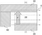
도 1을 참조하면, 본 발명의 제1 실시예에 따른 반도체 장치는 제1 전극(200), 제1 전극(200)과 이격된 제2 전극(300), 제1 전극(200)과 제2 전극(300) 사이에 개재되는 가변 저항 소자(100), 및 가변 저항 소자(100)에 이격된 채로 가변 저항 소자(100)에 전기장을 인가하는 도전체(400)를 포함할 수 있다.Referring to FIG. 1, a semiconductor device according to a first embodiment of the present invention includes a
가변 저항 소자(100)는 양단에 인가되는 전압 또는 전류에 따라 전기저항이 변화하여 적어도 서로 다른 두 저항 상태 사이에서 스위칭할 수 있는 구조를 포함할 수 있다. 예를 들어, 가변 저항 소자(100)는 스핀 전달 토크(Spin Transfer Torque; STT) 또는 자기장(Magnetic Field)에 의해 전기저항이 변하는 자기 터널 접합(Magnetic Tunnel Junction; MTJ) 구조를 포함할 수 있으며, 이외에도 산소 공공(Vacancy), 이온 등의 이동(Migration) 또는 물질의 상변화(Phase Change)에 의해 전기저항이 변하는 구조를 포함할 수 있다.The variable
제1 전극(200) 및 제2 전극(300)은 가변 저항 소자(100)에 전압 또는 전류를 인가할 수 있는 도전 물질을 포함할 수 있다. 예를 들어, 제1 및 제2 전극(200, 300)은 탄탈륨(Ta), 티타늄(Ti), 루테늄(Ru), 하프늄(Hf), 지르코늄(Zr), 알루미늄(Al), 텅스텐(W), 구리(Cu), 금(Au), 은(Ag), 백금(Pt), 니켈(Ni), 크롬(Cr), 코발트(Co) 등의 금속 또는 티타늄 질화물(TiN), 탄탈륨 질화물(TaN), 텅스텐 질화물(WN) 등의 금속 질화물을 포함하는 단일막이거나 이들의 조합으로 이루어진 다중막일 수 있다.The
도전체(400)는 가변 저항 소자(100)에 전기장을 인가하기 위한 것으로서 제1 및 제2 전극(200, 300)과 같은 도전 물질을 포함할 수 있으며, 이외에도 도핑된 실리콘 등의 다른 도전 물질을 포함할 수 있다. 특히, 도전체(400)에 전압이 인가되기만 하면 전기장이 생성될 수 있으므로 도전체(400)에 전류가 흐르지 않아도 무방하다. 즉, 도전체(400)는 폐쇄 회로(Closed Circuit)가 아닌 개방 회로(Open Circuit)로 구성될 수 있으며, 제1 및 제2 전극(200, 300)과 독립적으로 동작하거나 제1 및 제2 전극(200, 300)과 함께 동작할 수 있다.The
한편, 도전체(400)의 위치와 형태는 본 단면도에 도시된 것으로 한정되지 않으며, 요구되는 소자 특성 또는 제조 공정에 따라 다양하게 변형될 수 있다. 구체적으로 본 단면도에는 도전체(400)가 가변 저항 소자(100)의 좌측에 도시되어 있으나, 가변 저항 소자(100)의 우측 등 가변 저항 소자(100)에 전기장을 인가할 수 있는 다른 위치에 배치될 수도 있다. 특히, 가변 저항 소자(100)와 도전체(400)의 간격을 조절함으로써 가변 저항 소자(100)에 인가되는 전기장의 세기를 조절할 수 있으며, 필요에 따라 도전체(400)의 폭과 높이도 조절될 수 있다. 또한, 제1 전극(200)과 도전체(400)의 간격, 및 제2 전극(300)과 도전체(400)의 간격이 동일할 수 있으며, 경우에 따라 이들의 간격이 서로 다르더라도 무방하다.
Meanwhile, the position and shape of the
도 2a 내지 도 2d는 본 발명의 일 실시예에 따른 가변 저항 소자(100)를 도시하는 단면도이다.2A to 2D are sectional views showing a
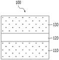
도 2a를 참조하면, 본 발명의 일 실시예에 따른 가변 저항 소자(100)는 제1 자성층(110), 제1 자성층(110)과 이격된 제2 자성층(130), 및 제1 자성층(110)과 제2 자성층(130) 사이에 개재되는 터널 장벽층(120)을 포함할 수 있다. 제1 자성층(110) 및 제2 자성층(130) 중 어느 하나는 자화 방향이 고정된 고정층(Pinned Layer)일 수 있으며, 다른 하나는 자화 방향이 가변적인 자유층(Free Layer)일 수 있다. 이때 가변 저항 소자(100)는 제1 및 제2 자성층(110, 130)의 자화 방향이 평행하면 저저항 상태로 될 수 있고, 이들의 자화 방향이 반평행하면 고저항 상태로 될 수 있다. 한편, 본 단면도에는 도시되지 않았으나 제1 자성층(110) 형성의 기초가 되는 기초층(Seed Layer)이 제1 자성층(110)의 하부에 배치될 수 있으며, 제2 자성층(130)을 보호하기 위한 보호층(Capping Layer)이 제2 자성층(130)의 상부에 배치될 수 있다.2A, a variable
여기서, 제1 및 제2 자성층(110, 130)은 철(Fe), 니켈(Ni), 코발트(Co), 가돌리늄(Gd), 디스프로슘(Dy) 등의 강자성 물질 또는 이들의 합금, 예컨대 코발트-철(CoFe), 니켈-철(NiFe), 코발트-철-니켈(CoFeNi) 등을 포함할 수 있으며, 제1 및 제2 자성층(110, 130)의 물성을 개선하기 위해 이러한 강자성 물질과 이들의 합금에 다양한 원소가 첨가될 수 있다. 예를 들어, 제1 및 제2 자성층(110, 130)은 코발트-철(CoFe)에 붕소(B)가 첨가된 코발트-철-붕소(CoFeB)로 이루어질 수 있으며, 붕소(B) 외에도 탄탈륨(Ta), 루테늄(Ru), 구리(Cu), 금(Au), 티타늄(Ti), 크롬(Cr), 은(Ag), 알루미늄(Al), 오스뮴(Os), 레늄(Re), 탄소(C), 산소(O), 질소(N), 팔라듐(Pd), 백금(Pt), 지르코늄(Zr), 아연(Zn), 이리듐(Ir), 텅스텐(W), 몰리브덴(Mo), 니오븀(Nb) 중 어느 하나 이상이 첨가될 수 있다. 한편, 제1 자성층(110)과 제2 자성층(130)은 동일한 물질로 이루어질 수도 있고, 서로 다른 물질로 이루어질 수도 있다.The first and second
또한, 터널 장벽층(120)은 마그네슘 산화물(MgO), 알루미늄 산화물(Al2O3), 실리콘 산화물(SiO2), 비스무스 산화물(Bi2O3), 마그네슘 질화물(MgN), 알루미늄 질화물(AlN), 실리콘 질화물(SiN), 불화 마그네슘(MgF2), 불화 칼슘(CaF2) 등의 비자성 절연 물질을 포함할 수 있다. 한편, 터널 장벽층(120)은 터널링 자기저항(Tunneling Magnetoresistance; TMR) 현상이 일어날 수 있을 정도의 얇은 두께를 가질 수 있으며, 상기 기초층 및 상기 보호층은 전술한 제1 및 제2 전극(200, 300)과 같이 금속, 금속 질화물 등의 도전 물질을 포함하는 단일막 또는 다중막일 수 있다.Further, the
도 2b를 참조하면, 본 발명의 일 실시예에 따른 가변 저항 소자(100)의 제1 자성층(110)은 하부 강자성층(112), 하부 강자성층(112)과 이격된 상부 강자성층(116), 및 하부 강자성층(112)과 상부 강자성층(116) 사이에 개재되는 비자성 스페이서층(114)을 포함하는 합성 반강자성층(Synthetic Anti-Ferromagnetic Layer; SAF Layer)일 수 있다. 이와 마찬가지로 제2 자성층(130)도 하부 강자성층(132), 하부 강자성층(132)과 이격된 상부 강자성층(136), 및 하부 강자성층(132)과 상부 강자성층(136) 사이에 개재되는 비자성 스페이서층(134)을 포함하는 합성 반강자성층(SAF Layer)일 수 있다.Referring to FIG. 2B, the first
여기서, 하부 강자성층(112, 132)과 상부 강자성층(116, 136)은 전술한 강자성 물질 또는 이들의 합금 등을 포함할 수 있으며, 이들은 반강자성적 또는 강자성적으로 결합(Coupling)될 수 있다. 또한, 비자성 스페이서층(114, 134)은 루테늄(Ru), 크롬(Cr), 구리(Cu), 티타늄(Ti), 텅스텐(W), 탄탈륨(Ta) 등을 포함할 수 있으며, 그 두께를 조절함으로써 하부 강자성층(112, 132)과 상부 강자성층(116, 136) 간의 교환 결합 특성을 조절할 수 있다. 한편, 본 단면도에는 제1 및 제2 자성층(110, 130) 모두가 합성 반강자성층(SAF Layer)인 것으로 도시되어 있으나, 제1 및 제2 자성층(110, 130) 중 어느 하나만 합성 반강자성층(SAF Layer)으로 구성될 수도 있다.Here, the lower
도 2c를 참조하면, 본 발명의 일 실시예에 따른 가변 저항 소자(100)는 자화 방향이 고정된 제1 자성층(110), 자화 방향이 가변적인 제2 자성층(130), 제1 자성층(110)과 제2 자성층(130) 사이에 개재되는 터널 장벽층(120), 및 제1 자성층(110)에 접하는 반강자성층(140)을 포함할 수 있다.Referring to FIG. 2C, the variable
여기서, 반강자성층(140)은 제1 자성층(110)의 자화 방향을 안정적으로 고정시키기 위한 것으로서 백금-망간(PtMn), 이리듐-망간(IrMn), 니켈-망간(NiMn), 철-망간(FeMn), 산화 니켈(NiO), 산화 코발트(CoO), 산화 철(Fe2O3), 염화 니켈(NiCl2), 염화 코발트(CoCl2), 염화 철(FeCl2) 등의 반강자성 물질을 포함할 수 있다. 한편, 본 실시예에서는 제1 자성층(110)이 고정층에 해당하므로 반강자성층(140)이 제1 자성층(110)의 하부에 접하도록 배치되어 있으나, 제2 자성층(130)이 고정층인 경우에는 반강자성층(140)이 제2 자성층(130)의 상부에 접하도록 배치될 수 있다.The
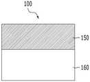
도 2d를 참조하면, 본 발명의 일 실시예에 따른 가변 저항 소자(100)는 가변 저항층(150), 및 가변 저항층(150)과 전기적으로 연결되는 스위칭층(160)을 포함할 수 있다. 가변 저항층(150)은 열에 의해 결정질 상태로 되거나 비정질 상태로 됨으로써 전기저항이 변하는 상변화 물질, 예컨대 게르마늄(Ge), 안티몬(Sb) 및 텔루륨(Te)이 소정 비율로 결합된 GST 등의 칼코게나이드(Chalcogenide) 계열의 물질을 포함할 수 있으며, 이외에도 인가되는 전압 또는 전류에 따라 그 내부에 필라멘트(Filament) 형태의 전류 통로가 생성되거나 소멸됨으로써 전기저항이 변하는 물질을 포함할 수 있다.2D, the variable
여기서, 전류 통로의 생성 또는 소멸에 따라 전기저항이 변하는 물질에는 STO(SrTiO3), BTO(BaTiO3), PCMO(Pr1-xCaxMnO3) 등의 페로브스카이트(Perovskite) 계열의 물질, 및 티타늄 산화물(TiO2), 하프늄 산화물(HfO2), 지르코늄 산화물(ZrO2), 알루미늄 산화물(Al2O3), 탄탈륨 산화물(Ta2O5), 니오븀 산화물(Nb2O5), 코발트 산화물(Co3O4), 니켈 산화물(NiO), 텅스텐 산화물(WO3), 란탄 산화물(La2O3) 등의 전이금속 산화물(Transition Metal Oxide, TMO) 등이 있다.Here, the material whose electric resistance changes depending on the generation or disappearance of the current path may be a perovskite series such as STO (SrTiO3 ), BTO (BaTiO3 ), PCMO (Pr1-x Cax MnO3 ) (TiO2 ), hafnium oxide (HfO2 ), zirconium oxide (ZrO2 ), aluminum oxide (Al2 O3 ), tantalum oxide (Ta2 O5 ), niobium oxide (Nb2 O5 ) , Transition metal oxide (TMO) such as cobalt oxide (Co3 O4 ), nickel oxide (NiO), tungsten oxide (WO3 ) and lanthanum oxide (La2 O3 ).
또한, 스위칭층(160)은 온/오프 동작이 가능한 트랜지스터 또는 단방향으로만 전류가 흐르는 다이오드를 포함할 수 있으며, 이외에도 비선형적인 전류-전압 특성을 갖는 비대칭 터널 장벽, 특정한 임계 온도에서 결정 구조의 변화 등에 의해 절연체에서 금속으로 혹은 금속에서 절연체로 전이됨으로써 전기저항이 급격히 변하는 금속-절연체 전이(Metal-Insulator Transition; MIT) 소자 또는 특정한 문턱 전압에서 스위칭이 가능한 오보닉(Ovonic) 스위칭 소자 등의 다른 선택 소자를 포함할 수 있다. 한편, 본 단면도에는 스위칭층(160)이 가변 저항층(150)의 하측에 접하는 것으로 도시되어 있으나, 스위칭층(160)이 가변 저항층(150)의 상측에 배치되거나 가변 저항층(150)에 직접 접하지 않아도 무방하다.
In addition, the
도 3은 본 발명의 제1 실시예에 따른 반도체 장치의 동작 방법을 설명하기 위한 단면도이다.3 is a cross-sectional view illustrating a method of operating the semiconductor device according to the first embodiment of the present invention.
도 3을 참조하면, 본 발명의 제1 실시예에 따른 반도체 장치의 제1 전극(200)에 음(-)의 전압을 인가하고, 제2 전극(300)에 양(+)의 전압을 인가하는 경우, 전자(e-)는 제1 전극(200)에서 제2 전극(300)으로 이동할 수 있다. 이때 전류의 방향은 전자의 이동 방향과 반대이므로 가변 저항 소자(100)의 상측에서 하측으로 전류가 흐를 수 있다. 한편, 제1 및 제2 전극(200, 300)에 인가되는 전압의 극성 및 크기는 다양하게 변화될 수 있다. 예를 들어, 제1 전극(200)에 양(+)의 전압을 인가하고, 제2 전극(300)에 음(-)의 전압을 인가할 수 있으며, 이에 따라 전류는 가변 저항 소자(100)의 하측에서 상측으로 흐를 수도 있다.3, a negative voltage is applied to the
여기서, 가변 저항 소자(100)의 좌측에 배치된 도전체(400)에 전압이 인가되지 않은 경우에는 가변 저항 소자(100)의 전체 영역으로 전류가 흐르게 되며, 이러한 경우 가변 저항 소자(100)를 고저항 상태에서 저저항 상태로 스위칭하거나, 반대로 저저항 상태에서 고저항 상태로 스위칭하는 데에 큰 전류가 소요된다. 그런데 도전체(400)에 양(+)의 전압을 인가하면 가변 저항 소자(100)의 좌측에서 우측으로 향하는 전기장(E)이 발생될 수 있다. 이때 전자(e-)에 전기장(E)의 방향(점선 화살표 참조)과 반대 방향으로 인력이 작용할 수 있으며, 이에 따라 전류는 가변 저항 소자(100) 내부에서 좌측의 국부적인 영역으로만 흐를 수 있다. 한편, 본 단면도에서 전자(e-)의 이동 방향 및 영역을 굵은 화살표로 표시하였으나 본 발명이 이에 한정되는 것은 아니다. 예를 들어, 전자(e-)는 제2 전극(300)에서 제1 전극(200)으로 이동할 수도 있으며, 도전체(400)에 음(-)의 전압을 인가하면 전기장(E)의 방향이 반대로 되어 전류는 가변 저항 소자(100) 내부에서 우측의 국부적인 영역으로만 흐를 수 있다.Here, when no voltage is applied to the
위와 같이 전류가 가변 저항 소자(100) 내의 국부적인 영역으로만 흐르는 경우, 가변 저항 소자(100)를 스위칭하는 데에 소요되는 전류가 감소하게 된다. 한편, 본 발명의 제1 실시예에 따른 반도체 장치의 도전체(400)는 제1 및 제2 전극(200, 300)과 독립적으로 동작할 수 있으므로 도전체(400)에는 제1 및 제2 전극(200, 300)에 인가되는 전압과 다른 전압이 인가될 수 있다. 특히, 도전체(400)에 인가되는 전압이 클수록 더 강한 전기장(E)이 발생될 수 있으며, 이에 따라 가변 저항 소자(100)의 스위칭 전류는 더욱 감소될 수 있다. 한편, 전기장(E)은 가변 저항 소자(100)에 흐르는 전류의 방향과 교차하는 방향으로 생성되면 족하며, 전기장(E)의 방향과 상기 전류의 방향이 반드시 수직일 필요는 없다.
When the current flows only in the local region in the variable
도 4는 본 발명의 제2 실시예에 따른 반도체 장치를 도시하는 단면도이다. 본 실시예를 설명함에 있어서, 전술한 제1 실시예와 실질적으로 동일한 부분에 대하여는 상세한 설명을 생략하기로 한다.4 is a cross-sectional view showing a semiconductor device according to a second embodiment of the present invention. In the following description of the present embodiment, a detailed description of parts that are substantially the same as those of the above-described first embodiment will be omitted.
도 4를 참조하면, 본 발명의 제2 실시예에 따른 반도체 장치는 제1 전극(200), 제1 전극(200)과 이격된 제2 전극(300), 제1 전극(200)과 제2 전극(300) 사이에 개재되는 가변 저항 소자(100), 및 가변 저항 소자(100)를 사이에 두고 한 쌍이 대칭적으로 배치되어 가변 저항 소자(100)에 전기장을 인가하는 한 쌍의 도전체(400)를 포함할 수 있다.Referring to FIG. 4, the semiconductor device according to the second embodiment of the present invention includes a
도전체(400)는 가변 저항 소자(100)에 전기장을 인가하기 위한 것으로서 제1 및 제2 전극(200, 300)과 같은 도전 물질을 포함할 수 있으며, 이외에도 도핑된 실리콘 등의 다른 도전 물질을 포함할 수 있다. 특히, 단결정 또는 다결정 실리콘에 불순물을 도핑함으로써 도전체(400)를 형성하는 경우에는 격자 부정합(Lattice Mismatch) 등에 의해 가변 저항 소자(100)에 인장 응력(Tensile Stress) 또는 압축 응력(Compressive Stress)이 가해질 수 있다. 이러한 응력은 가변 저항 소자(100)에 포함되는 자기 터널 접합(MTJ) 구조의 자기 이방성을 향상시키거나, 산소 공공 또는 이온 등의 이동도를 향상시킴으로써 가변 저항 소자(100)의 특성을 개선할 수 있다.
The
도 5는 본 발명의 제2 실시예에 따른 반도체 장치의 동작 방법을 설명하기 위한 단면도이다.5 is a cross-sectional view illustrating a method of operating a semiconductor device according to a second embodiment of the present invention.
도 5를 참조하면, 본 발명의 제2 실시예에 따른 반도체 장치의 제1 전극(200)에 음(-)의 전압을 인가하고, 제2 전극(300)에 양(+)의 전압을 인가하는 경우, 전자(e-)는 제1 전극(200)에서 제2 전극(300)으로 이동할 수 있다. 이때 전류의 방향은 전자의 이동 방향과 반대이므로 가변 저항 소자(100)의 상측에서 하측으로 전류가 흐를 수 있으며, 전술한 바와 같이 제1 및 제2 전극(200, 300)에 인가되는 전압의 극성 및 크기는 다양하게 변화될 수 있다.5, a negative voltage is applied to the
여기서, 한 쌍의 도전체(400) 각각은 서로 독립적으로 동작할 수 있으며, 도전체(400) 한 쌍 중 어느 하나와 다른 하나에 서로 다른 전압을 인가하면 가변 저항 소자(100)를 관통하는 전기장(E)이 발생될 수 있다. 예를 들어, 가변 저항 소자(100)의 좌측에 배치된 도전체(400)에 양(+)의 전압을 인가하고, 우측에 배치된 도전체(400)에 음(-)의 전압을 인가하면 가변 저항 소자(100)의 좌측에서 우측으로 향하는 전기장(E)이 발생될 수 있다. 이때 전자(e-)에 전기장(E)의 방향과 반대 방향으로 인력이 작용하여 전류가 가변 저항 소자(100) 내부에서 좌측의 국부적인 영역으로만 흐를 수 있다. 한편, 이와 반대로 가변 저항 소자(100)의 좌측에 배치된 도전체(400)에 음(-)의 전압을 인가하고, 우측에 배치된 도전체(400)에 양(+)의 전압을 인가하면 전기장(E)의 방향이 반대로 되어 전류는 가변 저항 소자(100) 내부에서 우측의 국부적인 영역으로만 흐를 수 있다.Here, each of the pair of
위와 같이 한 쌍의 도전체(400)에 인가되는 전압의 극성 및 크기는 다양하게 변화될 수 있으며, 도전체(400) 한 쌍 중 어느 하나와 다른 하나에 인가되는 전압의 차이가 클수록 더 강한 전기장(E)이 발생될 수 있다. 특히, 본 발명의 제2 실시예에 따른 반도체 장치의 도전체(400)는 가변 저항 소자(100)의 일측면 및 타측면에 한 쌍으로 배치되므로 전기장(E)의 세기가 더욱 강화되며, 이에 따라 가변 저항 소자(100)의 스위칭 전류를 크게 감소시킬 수 있다.
The polarity and magnitude of the voltage applied to the pair of
도 6a 및 도 6b는 본 발명의 제3 실시예에 따른 반도체 장치 및 이의 동작 방법을 설명하기 위한 단면도이다. 본 실시예를 설명함에 있어서, 전술한 제1 실시예와 실질적으로 동일한 부분에 대하여는 상세한 설명을 생략하기로 한다.6A and 6B are cross-sectional views illustrating a semiconductor device and an operation method thereof according to a third embodiment of the present invention. In the following description of the present embodiment, a detailed description of parts that are substantially the same as those of the above-described first embodiment will be omitted.
도 6a 및 도 6b를 참조하면, 본 발명의 제3 실시예에 따른 반도체 장치는 제1 전극(200), 제1 전극(200)과 이격된 제2 전극(300), 제1 전극(200)과 제2 전극(300) 사이에 개재되는 가변 저항 소자(100), 및 가변 저항 소자(100)에 이격된 채로 가변 저항 소자(100)에 전기장을 인가하는 도전체(400)를 포함할 수 있으며, 도전체(400)는 제2 전극(300)에 전기적으로 연결될 수 있다.6A and 6B, a semiconductor device according to a third embodiment of the present invention includes a
여기서, 도전체(400)는 제2 전극(300)에 직접 접속되거나(도 6a 참조), 배선(500) 등을 통해 접속될 수 있다(도 6b 참조). 이에 따라 제2 전극(300)에 인가되는 전압이 도전체(400)에도 인가될 수 있으며, 이러한 경우 도전체(400)에 전압을 인가하기 위한 별도의 회로 구성이 불필요하다. 이와 같이 도전체(400)를 제2 전극(300)에 전기적으로 연결하여 도전체(400)와 제2 전극(300)이 함께 동작되도록 구성함으로써 제조 공정을 단순화함과 동시에 제조 비용을 절감할 수 있다. 한편, 도전체(400)를 제2 전극(300)이 아닌 제1 전극(200)에 전기적으로 연결하여 도전체(400)와 제1 전극(200)이 함께 동작되도록 구성하여도 동일한 효과를 얻을 수 있다.
Here, the
도 7a 및 도 7b는 본 발명의 제4 실시예에 따른 반도체 장치 및 이의 동작 방법을 설명하기 위한 단면도이다. 본 실시예를 설명함에 있어서, 전술한 제2 실시예와 실질적으로 동일한 부분에 대하여는 상세한 설명을 생략하기로 한다.7A and 7B are cross-sectional views illustrating a semiconductor device and an operation method thereof according to a fourth embodiment of the present invention. In the following description of the present embodiment, a detailed description of the substantially same portions as those of the above-described second embodiment will be omitted.
도 7a 및 도 7b를 참조하면, 본 발명의 제4 실시예에 따른 반도체 장치는 제1 전극(200), 제1 전극(200)과 이격된 제2 전극(300), 제1 전극(200)과 제2 전극(300) 사이에 개재되는 가변 저항 소자(100), 및 가변 저항 소자(100)를 사이에 두고 한 쌍이 대칭적으로 배치되어 가변 저항 소자(100)에 전기장을 인가하는 한 쌍의 도전체(400)를 포함할 수 있으며, 도전체(400) 한 쌍 중 어느 하나는 제1 전극(200)에 전기적으로 연결될 수 있고, 다른 하나는 제2 전극(300)에 전기적으로 연결될 수 있다.7A and 7B, a semiconductor device according to a fourth embodiment of the present invention includes a
여기서, 한 쌍의 도전체(400) 각각은 제1 또는 제2 전극(200, 300)에 직접 접속되거나(도 7a 참조), 배선(500) 등을 통해 접속될 수 있다(도 7b 참조). 이에 따라 도전체(400) 한 쌍 중 어느 하나에는 제1 전극(200)에 인가되는 전압이 인가될 수 있고, 다른 하나에는 제2 전극(300)에 인가되는 전압이 인가될 수 있다. 이와 같이 도전체(400) 한 쌍 중 어느 하나를 제1 전극(200)에 전기적으로 연결하고, 다른 하나를 제2 전극(300)에 전기적으로 연결하는 경우, 도전체(400)에 전압을 인가하기 위한 별도의 회로 구성이 불필요하여 제조 공정을 단순화하면서 제조 비용을 절감할 수 있다.
Here, each of the pair of
도 8a 내지 도 8d는 본 발명의 일 실시예에 따른 반도체 장치의 구성예를 도시하는 단면도이다.8A to 8D are cross-sectional views showing a configuration example of a semiconductor device according to an embodiment of the present invention.
도 8a를 참조하면, 제1 전극(200), 제1 전극(200)과 이격된 제2 전극(300), 제1 전극(200)과 제2 전극(300) 사이에 개재되는 가변 저항 소자(100), 및 가변 저항 소자(100)의 일측면 또는 타측면 중 어느 하나 이상에 배치되어 가변 저항 소자(100)에 전기장을 인가하는 도전체(400)를 포함하는 본 발명의 일 실시예에 따른 반도체 장치의 제1 전극(200)은 트랜지스터에 전기적으로 연결될 수 있고, 제2 전극(300)은 비트 라인(660)에 접속될 수 있다.8A, a
상기 트랜지스터는 온/오프 동작을 하는 스위치로 사용되며, NMOS(N-channel Metal Oxide Semiconductor) 또는 PMOS(P-channel Metal Oxide Semiconductor) 트랜지스터일 수 있다. 이러한 트랜지스터는 기판(600) 상에 형성된 게이트 전극(610) 및 게이트 전극(610) 양측의 기판(600)에 형성된 소스 영역(620S) 및 드레인 영역(620D)을 포함할 수 있으며, 기판(600)과 게이트 전극(610) 사이에는 게이트 절연막(미도시됨)이 개재될 수 있다. 한편, 소스 영역(620S)은 콘택 플러그(630) 등을 통해 소스 라인(650)에 접속될 수 있고, 드레인 영역(620D)은 콘택 플러그(640) 등을 통해 제1 전극(200)에 접속될 수 있다.The transistor is used as a switch for on / off operation, and may be an NMOS (N-channel Metal Oxide Semiconductor) or a PMOS (P-channel Metal Oxide Semiconductor) transistor. These transistors may include a
여기서, 기판(600)은 실리콘(Si) 기판, 게르마늄(Ge) 기판, 실리콘-게르마늄(SiGe) 기판 또는 SOI(Silicon-On-Insulator) 기판일 수 있으며, 소스 영역(620S) 및 드레인 영역(620D)은 이온 주입 공정 등을 통해 기판(600)에 불순물을 주입함으로써 형성될 수 있다. 또한, 게이트 전극(610), 콘택 플러그(630, 640), 소스 라인(650) 및 비트 라인(660)은 금속, 금속 질화물 또는 도핑된 실리콘 등과 같은 도전 물질을 포함할 수 있다.Here, the
도 8b를 참조하면, 본 발명의 일 실시예에 따른 반도체 장치의 제1 전극(200)은 기판(700)에 매립된 게이트 전극(710)을 갖는 트랜지스터에 전기적으로 연결될 수 있고, 제2 전극(300)은 콘택 플러그(760) 등을 통해 비트 라인(780)에 접속될 수 있다. 게이트 전극(710)의 상부에는 보호층(730)이 형성될 수 있으며, 보호층(730) 양측의 기판(700)에는 불순물이 주입된 소스 영역(720S) 또는 드레인 영역(720D)이 형성될 수 있다. 한편, 소스 영역(720S)은 콘택 플러그(740) 등을 통해 소스 라인(770)에 접속될 수 있고, 드레인 영역(720D)은 콘택 플러그(750) 등을 통해 제1 전극(200)에 접속될 수 있다.8B, a
여기서, 기판(700)은 실리콘, 게르마늄 등을 포함하는 반도체 기판일 수 있고, 기판(700)과 게이트 전극(710) 사이에는 게이트 절연막(미도시됨)이 개재될 수 있다. 또한, 보호층(730)은 산화막 또는 질화막 계열의 물질을 포함할 수 있으며, 게이트 전극(710), 콘택 플러그(740, 750, 760), 소스 라인(770) 및 비트 라인(780)은 전술한 바와 같은 도전 물질을 포함할 수 있다.Here, the
도 8c를 참조하면, 본 발명의 일 실시예에 따른 반도체 장치의 제1 전극(200)은 수직형 채널층(800)을 갖는 트랜지스터에 전기적으로 연결될 수 있고, 제2 전극(300)은 콘택 플러그(820) 등을 통해 비트 라인(830)에 접속될 수 있다. 게이트 전극(810)은 채널층(800) 측면의 적어도 일부와 접할 수 있으며, 채널층(800)과 게이트 전극(810) 사이에는 게이트 절연막(미도시됨)이 개재될 수 있다. 한편, 채널층(800)의 상단은 제1 전극(200)에 접속될 수 있고, 채널층(800)의 하단은 소스 라인(840)에 접속될 수 있다.8C, a
여기서, 채널층(800)은 실리콘, 게르마늄 등과 같은 반도체 물질을 포함할 수 있으며, 채널층(800)의 상단 및 하단에는 불순물이 주입된 접합 영역(미도시됨)이 형성될 수 있다. 또한, 게이트 전극(810), 콘택 플러그(820), 비트 라인(830) 및 소스 라인(840)은 전술한 바와 같은 도전 물질을 포함할 수 있다.Here, the
도 8d를 참조하면, 본 발명의 일 실시예에 따른 반도체 장치의 제1 전극(200)은 선택 소자(900)의 일단에 전기적으로 연결될 수 있고, 제2 전극(300)은 콘택 플러그(910) 등을 통해 비트 라인(920)에 접속될 수 있다. 선택 소자(900)의 타단은 워드 라인(930)에 접속될 수 있으며, 비트 라인(920)과 워드 라인(930)은 서로 교차하는 방향으로 연장될 수 있다.8D, the
여기서, 선택 소자(900)는 쇼트키(Schottky) 다이오드, PN 다이오드, PIN 다이오드 또는 MIM 다이오드 등과 같은 다이오드일 수 있으며, 이외에도 비대칭 터널 장벽, 금속-절연체 전이(MIT) 소자 또는 오보닉 스위칭 소자 등을 포함할 수 있다. 또한, 콘택 플러그(910), 비트 라인(920) 및 워드 라인(930)은 전술한 바와 같은 도전 물질을 포함할 수 있다.
Here, the
도 9는 본 발명의 일 실시예에 따른 마이크로프로세서(1000)의 구성도이다.9 is a configuration diagram of a
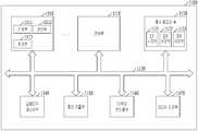
도 9에 도시된 바와 같이, 마이크로프로세서(Micro Processor Unit, 1000)는 다양한 외부 장치로부터 데이터를 받아서 처리한 후, 그 결과를 외부 장치로 보내는 일련의 과정을 제어하고 조정하는 일을 수행할 수 있으며 기억부(1010), 연산부(1020) 및 제어부(1030)를 포함할 수 있다. 마이크로프로세서(1000)는 중앙 처리 장치(Central Processing Unit; CPU), 그래픽 처리 장치(Graphic Processing Unit; GPU), 디지털 신호 처리 장치(Digital Signal Processor; DSP), 어플리케이션 프로세서(Application Processor; AP) 등 각종 처리장치일 수 있다.As shown in FIG. 9, a
기억부(1010)는 프로세서 레지스터(Processor Register) 또는 레지스터(Register) 등으로 마이크로프로세서(1000) 내에서 데이터를 저장하는 부분이며, 데이터 레지스터, 주소 레지스터, 부동 소수점 레지스터 등의 다양한 레지스터를 포함할 수 있다. 기억부(1010)는 연산부(1020)에서 연산을 수행하는 데이터나 수행결과 데이터, 수행을 위한 데이터가 저장되어 있는 주소를 일시적으로 저장하는 역할을 수행할 수 있다.The
기억부(1010)는 전술한 반도체 장치의 실시예들 중 하나를 포함할 수 있다. 전술한 실시예에 따른 반도체 장치를 포함하는 기억부(1010)는 제1 전극, 상기 제1 전극과 이격된 제2 전극, 상기 제1 전극과 상기 제2 전극 사이에 개재되는 가변 저항 소자, 및 상기 가변 저항 소자의 일측면 또는 타측면 중 어느 하나 이상에 배치되어 상기 가변 저항 소자에 이격된 채로 전기장을 인가하는 도전체를 포함할 수 있다. 본 실시예에 따른 기억부(1010)는 상기 도전체를 통해 가변 저항 소자에 전기장을 인가하여 전류가 가변 저항 소자 내부에서 국부적인 영역으로 주입되도록 함으로써 가변 저항 소자의 스위칭 전류를 감소시킬 수 있으므로 마이크로프로세서(1000)의 전력 소모를 줄일 수 있다.The
연산부(1020)는 마이크로프로세서(1000)의 내부에서 연산을 수행하는 부분으로 제어부(1030)가 명령을 해독한 결과에 따라 여러 가지 사칙 연산 또는 논리 연산을 수행한다. 연산부(1020)는 하나 이상의 산술 논리 연산 장치(Arithmetic and Logic Unit; ALU)를 포함할 수 있다.The
제어부(1030)는 기억부(1010), 연산부(1020) 및 마이크로프로세서(1000) 외부 장치로부터의 신호를 수신하여 명령의 추출이나 해독, 입력이나 출력의 제어 등을 수행하고, 프로그램으로 나타내어진 처리를 실행한다.The
본 실시예에 따른 마이크로프로세서(1000)는 기억부(1010) 이외에 외부 장치로부터 입력되거나 외부 장치로 출력할 데이터를 임시 저장할 수 있는 캐시 메모리부(1040)를 추가로 포함할 수 있으며, 이 경우 버스 인터페이스(1050)를 통해 기억부(1010), 연산부(1020) 및 제어부(1030)와 데이터를 주고 받을 수 있다.
The
도 10은 본 발명의 일 실시예에 따른 프로세서(1100)의 구성도이다.10 is a configuration diagram of a
도 10에 도시된 바와 같이, 프로세서(1100)는 다양한 외부 장치로부터 데이터를 받아서 처리한 후, 그 결과를 외부 장치로 보내는 일련의 과정을 제어하고 조정하는 일을 수행하는 마이크로프로세서 이외의 다양한 기능을 포함하여 성능을 향상시킬 수 있으며, 코어부(1110), 캐시 메모리부(1120) 및 버스 인터페이스(1130)를 포함할 수 있다. 본 실시예의 코어부(1110)는 외부 장치로부터 입력된 데이터를 산술 논리 연산하는 부분으로 기억부(1111), 연산부(1112), 제어부(1113)를 포함할 수 있다. 프로세서(1100)는 멀티 코어 프로세서(Multi Core Processor), 그래픽 처리 장치(Graphic Processing Unit; GPU), 어플리케이션 프로세서(Application Processor; AP) 등 각종 시스템 온 칩(System on Chip; SoC)일 수 있다.As shown in FIG. 10, the
기억부(1111)는 프로세서 레지스터(Processor Register) 또는 레지스터(Register) 등으로 프로세서(1100) 내에서 데이터를 저장하는 부분이며, 데이터 레지스터, 주소 레지스터, 부동 소수점 레지스터 등의 다양한 레지스터를 포함할 수 있다. 기억부(1111)는 연산부(1112)에서 연산을 수행하는 데이터나 수행결과 데이터, 수행을 위한 데이터가 저장되어 있는 주소를 일시적으로 저장하는 역할을 수행할 수 있다. 연산부(1112)는 프로세서(1100)의 내부에서 연산을 수행하는 부분으로 제어부(1113)가 명령을 해독한 결과에 따라 여러 가지 사칙 연산 또는 논리 연산을 수행한다. 연산부(1112)는 하나 이상의 산술 논리 연산 장치(Arithmetic and Logic Unit; ALU)를 포함할 수 있다. 제어부(1113)는 기억부(1111), 연산부(1112) 및 프로세서(1100) 외부 장치로부터의 신호를 수신하여 명령의 추출이나 해독, 입력이나 출력의 제어 등을 수행하고, 프로그램으로 나타내어진 처리를 실행한다.The
캐시 메모리부(1120)는 고속으로 동작하는 코어부(1110)와 저속으로 동작하는 외부 장치 간의 데이터 처리 속도 차이를 보완하기 위해 임시로 데이터를 저장하는 부분으로 1차 저장부(1121), 2차 저장부(1122) 및 3차 저장부(1123)를 포함할 수 있다. 일반적으로 캐시 메모리부(1120)는 1차, 2차 저장부(1121, 1122)를 포함하고 고용량이 필요할 경우 3차 저장부(1123)를 포함할 수 있으며, 필요 시에는 더 많은 저장부를 포함할 수 있다. 즉, 캐시 메모리부(1120)에 포함되는 저장부의 개수는 설계에 따라 달라질 수 있다. 여기서, 1차, 2차, 3차 저장부(1121, 1122, 1123)의 데이터 저장 및 판별 처리 속도는 같을 수도 있고 다를 수도 있으며, 각 저장부의 처리 속도가 다른 경우 1차 저장부(1121)의 속도가 제일 빠를 수 있다.The
캐시 메모리부(1120)의 1차, 2차, 3차 저장부(1121, 1122, 1123) 중 어느 하나 이상의 저장부는 전술한 반도체 장치의 실시예들 중 하나를 포함할 수 있다. 전술한 실시예에 따른 반도체 장치를 포함하는 캐시 메모리부(1120)는 제1 전극, 상기 제1 전극과 이격된 제2 전극, 상기 제1 전극과 상기 제2 전극 사이에 개재되는 가변 저항 소자, 및 상기 가변 저항 소자의 일측면 또는 타측면 중 어느 하나 이상에 배치되어 상기 가변 저항 소자에 이격된 채로 전기장을 인가하는 도전체를 포함할 수 있다. 본 실시예에 따른 캐시 메모리부(1120)는 상기 도전체를 통해 가변 저항 소자에 전기장을 인가하여 전류가 가변 저항 소자 내부에서 국부적인 영역으로 주입되도록 함으로써 가변 저항 소자의 스위칭 전류를 감소시킬 수 있으므로 프로세서(1100)의 전력 소모를 줄일 수 있다.Any one or more of the primary, secondary, and
버스 인터페이스(1130)는 코어부(1110)와 캐시 메모리부(1120)를 연결하여 데이터를 효율적으로 전송할 수 있게 해주는 부분이다. 한편, 본 구성도에는 캐시 메모리부(1120)의 1차, 2차, 3차 저장부(1121, 1122, 1123)가 모두 캐시 메모리부(1120)의 내부에 구성되는 것으로 도시되어 있으나, 캐시 메모리부(1120)의 1차 저장부(1121)는 코어부(1110)의 내부에 구성될 수도 있다. 이때 캐시 메모리부(1120)의 2차, 3차 저장부(1122, 1123)는 코어부(1110)의 외부에 구성하여 처리 속도 보완을 위한 기능을 더 강화할 수 있다.The
본 실시예에 따른 프로세서(1100)는 다수의 코어부(1110)를 포함할 수 있으며, 다수의 코어부(1110)는 캐시 메모리부(1120)를 공유할 수 있다. 다수의 코어부(1110)와 캐시 메모리부(1120)는 버스 인터페이스(1130)를 통해 연결될 수 있다. 다수의 코어부(1110)는 모두 전술한 코어부의 구성과 동일하게 구성될 수 있다. 다수의 코어부(1110)를 포함하는 경우 캐시 메모리부(1120)의 1차 저장부(1121)는 다수의 코어부(1110)의 개수에 대응하여 각각의 코어부(1110) 내에 구성되고, 2차 저장부(1122)와 3차 저장부(1123)는 다수의 코어부(1110)의 외부에 버스 인터페이스(1130)를 통해 공유되도록 구성될 수 있다.The
본 실시예에 따른 프로세서(1100)는 데이터를 저장하는 임베디드(Embedded) 메모리부(1140), 외부 장치와 유선 또는 무선으로 데이터를 송수신할 수 있는 통신모듈부(1150), 외부 기억장치를 구동하는 메모리 컨트롤부(1160), 외부 인터페이스 장치에 프로세서(1100)에서 처리된 데이터나 외부 입력장치에서 입력된 데이터를 가공하고 출력하는 미디어처리부(1170)를 추가로 포함할 수 있으며, 이외에도 다수의 모듈을 포함할 수 있다. 이 경우 추가되는 다수의 모듈들은 버스 인터페이스(1130)를 통해 코어부(1110), 캐시 메모리부(1120) 및 상호 간에 데이터를 주고 받을 수 있다.The
임베디드 메모리부(1140)는 휘발성 메모리뿐만 아니라 비휘발성 메모리도 포함할 수 있다. 휘발성 메모리는 DRAM(Dynamic Random Access Memory), Mobile DRAM, SRAM(Static Random Access Memory) 등을 포함할 수 있으며, 비휘발성 메모리는 ROM(Read Only Memory), NOR 플래시 메모리, NAND 플래시 메모리, 상변화 메모리(Phase-change Random Access Memory; PRAM), 저항성 메모리(Resistive Random Access Memory; RRAM), 스핀 주입 메모리(Spin Transfer Torque Random Access Memory; STT-RAM), 자기 메모리(Magnetic Random Access Memory; MRAM) 등을 포함할 수 있다.The embedded
통신모듈부(1150)는 유선 네트워크와 연결할 수 있는 모듈과 무선 네트워크와 연결할 수 있는 모듈을 모두 포함할 수 있다. 유선 네트워크 모듈은 유선 랜(Local Area Network; LAN), USB(Universal Serial Bus), 이더넷(Ethernet), 전력선 통신(Power Line Communication; PLC) 등을 포함할 수 있으며, 무선 네트워크 모듈은 적외선 통신(Infrared Data Association; IrDA), 코드분할 다중접속(Code Division Multiple Access; CDMA), 시분할 다중접속(Time Division Multiple Access; TDMA), 주파수분할 다중접속(Frequency Division Multiple Access; FDMA), 무선 랜(Wireless LAN), 유비쿼터스 센서 네트워크(Ubiquitous Sensor Network; USN), RFID(Radio Frequency IDentification), NFC(Near Field Communication), 지그비(Zigbee), 블루투스(Bluetooth), 와이브로(Wireless Broadband Internet; WiBro), LTE(Long Term Evolution), 고속 하향 패킷 접속(High Speed Downlink Packet Access; HSDPA), 광대역 코드분할 다중접속(Wideband CDMA; WCDMA), 초광대역 통신(Ultra WideBand; UWB) 등을 포함할 수 있다.The
메모리 컨트롤부(1160)는 프로세서(1100)와 서로 다른 통신 규격에 따라 동작하는 외부 저장장치 사이에 전송되는 데이터를 관리하기 위한 것으로 각종 메모리 컨트롤러, 예컨대 IDE(Integrated Device Electronics), SATA(Serial Advanced Technology Attachment), SCSI(Small Computer System Interface), RAID(Redundant Array of Independent Disks), SSD(Solid State Drive), PCMCIA(Personal Computer Memory Card International Association), eSATA(external SATA), USB(Universal Serial Bus), SD(Secure Digital) 카드, 미니 SD(mini Secure Digital) 카드, 마이크로 SD(micro Secure Digital) 카드, 고용량 SD(Secure Digital High Capacity; SDHC) 카드, 메모리 스틱(Memory Stick), 컴팩트 플래시(Compact Flash; CF) 카드, 스마트 미디어(Smart Media; SM) 카드, 멀티미디어 카드(Multi-Media Card; MMC), 내장 멀티미디어 카드(embedded MMC; eMMC) 등을 제어하는 컨트롤러를 포함할 수 있다.The
미디어처리부(1170)는 프로세서(1100)에서 처리된 데이터나 외부 입력장치에서 입력된 데이터를 가공하여 영상, 음성 및 기타 형태로 전달되도록 외부 인터페이스 장치로 출력하는 그래픽 처리 장치(Graphic Processing Unit; GPU), 디지털 신호 처리 장치(Digital Signal Processor; DSP), 고선명 오디오(High Definition Audio; HD Audio), 고선명 멀티미디어 인터페이스(High Definition Multimedia Interface; HDMI) 컨트롤러 등을 포함할 수 있다.
The
도 11은 본 발명의 일 실시예에 따른 시스템(1200)의 구성도이다.11 is a configuration diagram of a
도 11에 도시된 바와 같이, 시스템(1200)은 데이터를 처리하는 장치로 데이터에 대하여 일련의 조작을 수행하기 위해 입력, 처리, 출력, 통신, 저장 등을 수행할 수 있으며, 프로세서(1210), 주기억 장치(1220), 보조기억 장치(1230), 인터페이스 장치(1240)를 포함할 수 있다. 본 실시예에 따른 시스템(1200)은 컴퓨터(Computer), 서버(Server), PDA(Personal Digital Assistant), 태블릿 PC(Tablet Personal Computer), 휴대용 컴퓨터(Portable Computer), 무선 전화(Wireless Phone), 휴대 전화(Mobile Phone), 스마트폰(Smart Phone), 디지털 음악 재생기기(Digital Music Player), PMP(Portable Multimedia Player), 카메라(Camera), 위성항법장치(Global Positioning System; GPS), 비디오 카메라(Video Camera), 음성 녹음기(Voice Recorder), 텔레매틱스(Telematics), AV 시스템(Audio Visual System), 스마트 TV(Smart Television) 등의 각종 전자 시스템일 수 있다.As shown in FIG. 11, the
프로세서(1210)는 입력된 명령어의 해석과 시스템(1200)에 저장된 자료의 연산, 비교 등의 처리를 제어하는 시스템(1200)의 핵심적인 구성으로 마이크로프로세서(Micro Processor Unit; MPU), 중앙 처리 장치(Central Processing Unit; CPU), 싱글/멀티 코어 프로세서(Single/Multi Core Processor), 어플리케이션 프로세서(Application Processor; AP), 그래픽 처리 장치(Graphic Processing Unit; GPU), 디지털 신호 처리 장치(Digital Signal Processor; DSP) 등으로 구성될 수 있다.The
주기억 장치(1220)는 프로그램이 실행될 때 보조기억 장치(1230)로부터 프로그램이나 자료를 이동시켜 실행시킬 수 있는 기억 장소로 전원이 끊어져도 기억된 내용이 보존되며, 전술한 반도체 장치의 실시예들 중 하나를 포함할 수 있다. 전술한 실시예에 따른 반도체 장치를 포함하는 주기억 장치(1220)는 제1 전극, 상기 제1 전극과 이격된 제2 전극, 상기 제1 전극과 상기 제2 전극 사이에 개재되는 가변 저항 소자, 및 상기 가변 저항 소자의 일측면 또는 타측면 중 어느 하나 이상에 배치되어 상기 가변 저항 소자에 이격된 채로 전기장을 인가하는 도전체를 포함할 수 있다. 본 실시예에 따른 주기억 장치(1220)는 상기 도전체를 통해 가변 저항 소자에 전기장을 인가하여 전류가 가변 저항 소자 내부에서 국부적인 영역으로 주입되도록 함으로써 가변 저항 소자의 스위칭 전류를 감소시킬 수 있으므로 시스템(1200)의 전력 소모를 줄일 수 있다.The
주기억 장치(1220)는 전원이 꺼지면 모든 내용이 지워지는 휘발성 특성을 갖는 SRAM(Static Random Access Memory), DRAM(Dynamic Random Access Memory) 등을 더 포함할 수 있다. 이와 달리, 주기억 장치(1220)는 본 발명의 실시예에 따른 반도체 장치를 포함하지 않고, 전원이 꺼지면 모든 내용이 지워지는 휘발성 특성을 갖는 SRAM(Static Random Access Memory), DRAM(Dynamic Random Access Memory) 등을 포함할 수도 있다.The
보조기억 장치(1230)는 프로그램 코드나 데이터를 저장하기 위한 기억 장소로 주기억 장치(1220)보다 속도는 느리지만 많은 자료를 저장할 수 있으며, 전술한 반도체 장치의 실시예들 중 하나를 포함할 수 있다. 전술한 실시예에 따른 반도체 장치를 포함하는 보조기억 장치(1230)는 제1 전극, 상기 제1 전극과 이격된 제2 전극, 상기 제1 전극과 상기 제2 전극 사이에 개재되는 가변 저항 소자, 및 상기 가변 저항 소자의 일측면 또는 타측면 중 어느 하나 이상에 배치되어 상기 가변 저항 소자에 이격된 채로 전기장을 인가하는 도전체를 포함할 수 있다. 본 실시예에 따른 보조기억 장치(1230)는 상기 도전체를 통해 가변 저항 소자에 전기장을 인가하여 전류가 가변 저항 소자 내부에서 국부적인 영역으로 주입되도록 함으로써 가변 저항 소자의 스위칭 전류를 감소시킬 수 있으므로 시스템(1200)의 전력 소모를 줄일 수 있다.The
보조기억 장치(1230)는 자기 테이프, 자기 디스크, 레이저 디스크, 광자기 디스크, SSD(Solid State Drive), USB 메모리(Universal Serial Bus Memory; USB Memory), SD(Secure Digital) 카드, 미니 SD(mini Secure Digital) 카드, 마이크로 SD(micro Secure Digital) 카드, 고용량 SD(Secure Digital High Capacity; SDHC) 카드, 메모리 스틱(Memory Stick), 컴팩트 플래시(Compact Flash; CF) 카드, 스마트 미디어(Smart Media; SM) 카드, 멀티미디어 카드(Multi-Media Card; MMC), 내장 멀티미디어 카드(embedded MMC; eMMC) 등의 데이터 저장 시스템을 더 포함할 수 있다. 이와 달리, 보조기억 장치(1230)는 본 발명의 실시예에 따른 반도체 장치를 포함하지 않고, 자기 테이프, 자기 디스크, 레이저 디스크, 광자기 디스크, SSD(Solid State Drive), USB 메모리(Universal Serial Bus Memory; USB Memory), SD(Secure Digital) 카드, 미니 SD(mini Secure Digital) 카드, 마이크로 SD(micro Secure Digital) 카드, 고용량 SD(Secure Digital High Capacity; SDHC) 카드, 메모리 스틱(Memory Stick), 컴팩트 플래시(Compact Flash; CF) 카드, 스마트 미디어(Smart Media; SM) 카드, 멀티미디어 카드(Multi-Media Card; MMC), 내장 멀티미디어 카드(embedded MMC; eMMC) 등의 데이터 저장 시스템을 포함할 수도 있다.The
인터페이스 장치(1240)는 시스템(1200)과 외부 장치 간에 명령 및 데이터 등을 교환하기 위한 장치일 수 있으며, 키패드(Keypad), 키보드(Keyboard), 마우스(Mouse), 스피커(Speaker), 마이크(Mike), 각종 디스플레이(Display) 장치, 각종 휴먼 인터페이스 장치(Human Interface Device; HID) 또는 통신 장치일 수 있다. 상기 통신 장치는 유선 네트워크와 연결할 수 있는 모듈과 무선 네트워크와 연결할 수 있는 모듈을 모두 포함할 수 있다. 유선 네트워크 모듈은 유선 랜(Local Area Network; LAN), USB(Universal Serial Bus), 이더넷(Ethernet), 전력선 통신(Power Line Communication; PLC) 등을 포함할 수 있으며, 무선 네트워크 모듈은 적외선 통신(Infrared Data Association; IrDA), 코드분할 다중접속(Code Division Multiple Access; CDMA), 시분할 다중접속(Time Division Multiple Access; TDMA), 주파수분할 다중접속(Frequency Division Multiple Access; FDMA), 무선 랜(Wireless LAN), 유비쿼터스 센서 네트워크(Ubiquitous Sensor Network; USN), RFID(Radio Frequency IDentification), NFC(Near Field Communication), 지그비(Zigbee), 블루투스(Bluetooth), 와이브로(Wireless Broadband Internet; WiBro), LTE(Long Term Evolution), 고속 하향 패킷 접속(High Speed Downlink Packet Access; HSDPA), 광대역 코드분할 다중접속(Wideband CDMA; WCDMA), 초광대역 통신(Ultra WideBand; UWB) 등을 포함할 수 있다.
The
도 12는 본 발명의 일 실시예에 따른 데이터 저장 시스템(1300)의 구성도이다.12 is a configuration diagram of a
도 12에 도시된 바와 같이, 데이터 저장 시스템(1300)은 데이터를 저장하기 위한 구성으로 비휘발성 특성을 갖는 저장 장치(1310), 이를 제어하는 컨트롤러(1320) 및 외부 장치와 연결하는 인터페이스(1330)를 포함할 수 있다. 본 실시예에 따른 데이터 저장 시스템(1300)은 하드 디스크 드라이브(Hard Disk Drive; HDD), SSD(Solid State Drive), CD(Compact Disc), DVD(Digital Versatile Disc) 등의 디스크 형태이거나, USB 메모리(Universal Serial Bus Memory; USB Memory), SD(Secure Digital) 카드, 미니 SD(mini Secure Digital) 카드, 마이크로 SD(micro Secure Digital) 카드, 고용량 SD(Secure Digital High Capacity; SDHC) 카드, 메모리 스틱(Memory Stick), 컴팩트 플래시(Compact Flash; CF) 카드, 스마트 미디어(Smart Media; SM) 카드, 멀티미디어 카드(Multi-Media Card; MMC), 내장 멀티미디어 카드(embedded MMC; eMMC) 등의 카드 형태일 수 있다.12, the
컨트롤러(1320)는 저장 장치(1310)와 인터페이스(1330) 사이에서 데이터의 교환을 제어할 수 있다. 이를 위해 컨트롤러(1320)는 데이터 저장 시스템(1300)의 외부에서 인터페이스(1330)를 통해 입력된 명령어들을 연산 및 처리하기 위한 프로세서(1321)를 포함할 수 있다.The
인터페이스(1330)는 데이터 저장 시스템(1300)과 외부 장치 간에 명령 및 데이터 등을 교환하기 위한 것으로 데이터 저장 시스템(1300)이 카드 형태인 경우, USB 메모리(Universal Serial Bus Memory; USB Memory), SD(Secure Digital) 카드, 미니 SD(mini Secure Digital) 카드, 마이크로 SD(micro Secure Digital) 카드, 고용량 SD(Secure Digital High Capacity; SDHC) 카드, 메모리 스틱(Memory Stick), 컴팩트 플래시(Compact Flash; CF) 카드, 스마트 미디어(Smart Media; SM) 카드, 멀티미디어 카드(Multi-Media Card; MMC), 내장 멀티미디어 카드(embedded MMC; eMMC) 등과 호환될 수 있다. 또한, 인터페이스(1330)는 데이터 저장 시스템(1300)이 디스크 형태인 경우, IDE(Integrated Device Electronics), SATA(Serial Advanced Technology Attachment), SCSI(Small Computer System Interface), RAID(Redundant Array of Independent Disks), PCMCIA(Personal Computer Memory Card International Association), eSATA(external SATA), USB(Universal Serial Bus) 등과 호환될 수 있다.The
본 실시예에 따른 데이터 저장 시스템(1300)은 저장 장치(1310)와 인터페이스(1330) 간에 데이터를 효율적으로 전달하기 위한 임시 저장 장치(1340)를 포함할 수 있다. 저장 장치(1310) 또는 데이터를 임시로 저장하는 임시 저장 장치(1340)는 전술한 반도체 장치의 실시예들 중 하나를 포함할 수 있다. 전술한 실시예에 따른 반도체 장치를 포함하는 저장 장치(1310) 또는 임시 저장 장치(1340)는 제1 전극, 상기 제1 전극과 이격된 제2 전극, 상기 제1 전극과 상기 제2 전극 사이에 개재되는 가변 저항 소자, 및 상기 가변 저항 소자의 일측면 또는 타측면 중 어느 하나 이상에 배치되어 상기 가변 저항 소자에 이격된 채로 전기장을 인가하는 도전체를 포함할 수 있다. 본 실시예에 따른 저장 장치(1310) 또는 임시 저장 장치(1340)는 상기 도전체를 통해 가변 저항 소자에 전기장을 인가하여 전류가 가변 저항 소자 내부에서 국부적인 영역으로 주입되도록 함으로써 가변 저항 소자의 스위칭 전류를 감소시킬 수 있으므로 데이터 저장 시스템(1300)의 전력 소모를 줄일 수 있다.
The
도 13은 본 발명의 일 실시예에 따른 메모리 시스템(1400)의 구성도이다.13 is a configuration diagram of a
도 13에 도시된 바와 같이, 메모리 시스템(1400)은 데이터를 저장하기 위한 구성으로 비휘발성 특성을 갖는 메모리(1410), 이를 제어하는 메모리 컨트롤러(1420) 및 외부 장치와 연결하는 인터페이스(1430)를 포함할 수 있다. 본 실시예에 따른 메모리 시스템(1400)은 USB 메모리(Universal Serial Bus Memory; USB Memory), SD(Secure Digital) 카드, 미니 SD(mini Secure Digital) 카드, 마이크로 SD(micro Secure Digital) 카드, 고용량 SD(Secure Digital High Capacity; SDHC) 카드, 메모리 스틱(Memory Stick), 컴팩트 플래시(Compact Flash; CF) 카드, 스마트 미디어(Smart Media; SM) 카드, 멀티미디어 카드(Multi-Media Card; MMC), 내장 멀티미디어 카드(embedded MMC; eMMC) 등의 카드 형태일 수 있다.13, the
데이터를 저장하는 메모리(1410)는 전술한 반도체 장치의 실시예들 중 하나를 포함할 수 있다. 전술한 실시예에 따른 반도체 장치를 포함하는 메모리(1410)는 제1 전극, 상기 제1 전극과 이격된 제2 전극, 상기 제1 전극과 상기 제2 전극 사이에 개재되는 가변 저항 소자, 및 상기 가변 저항 소자의 일측면 또는 타측면 중 어느 하나 이상에 배치되어 상기 가변 저항 소자에 이격된 채로 전기장을 인가하는 도전체를 포함할 수 있다. 본 실시예에 따른 메모리(1410)는 상기 도전체를 통해 가변 저항 소자에 전기장을 인가하여 전류가 가변 저항 소자 내부에서 국부적인 영역으로 주입되도록 함으로써 가변 저항 소자의 스위칭 전류를 감소시킬 수 있으므로 메모리 시스템(1400)의 전력 소모를 줄일 수 있다.The
메모리(1410)는 비휘발성 특성을 갖는 ROM(Read Only Memory), NOR 플래시 메모리, NAND 플래시 메모리, 상변화 메모리(Phase-change Random Access Memory; PRAM), 저항성 메모리(Resistive Random Access Memory; RRAM), 스핀 주입 메모리(Spin Transfer Torque Random Access Memory; STT-RAM), 자기 메모리(Magnetic Random Access Memory; MRAM) 등을 더 포함할 수 있다.The
메모리 컨트롤러(1420)는 메모리(1410)와 인터페이스(1430) 사이에서 데이터의 교환을 제어할 수 있다. 이를 위해 메모리 컨트롤러(1420)는 메모리 시스템(1400)의 외부에서 인터페이스(1430)를 통해 입력된 명령어들을 연산 및 처리하기 위한 프로세서(1421)를 포함할 수 있다.
인터페이스(1430)는 메모리 시스템(1400)과 외부 장치 간에 명령 및 데이터 등을 교환하기 위한 것으로 USB 메모리(Universal Serial Bus Memory; USB Memory), SD(Secure Digital) 카드, 미니 SD(mini Secure Digital) 카드, 마이크로 SD(micro Secure Digital) 카드, 고용량 SD(Secure Digital High Capacity; SDHC) 카드, 메모리 스틱(Memory Stick), 컴팩트 플래시(Compact Flash; CF) 카드, 스마트 미디어(Smart Media; SM) 카드, 멀티미디어 카드(Multi-Media Card; MMC), 내장 멀티미디어 카드(embedded MMC; eMMC) 등과 호환될 수 있다.The
본 실시예에 따른 메모리 시스템(1400)은 메모리(1410)와 인터페이스(1430) 간에 데이터를 효율적으로 전달하기 위한 버퍼 메모리(1440)를 포함할 수 있다. 데이터를 임시로 저장하는 버퍼 메모리(1440)는 전술한 반도체 장치의 실시예들 중 하나를 포함할 수 있다. 전술한 실시예에 따른 반도체 장치를 포함하는 버퍼 메모리(1440)는 제1 전극, 상기 제1 전극과 이격된 제2 전극, 상기 제1 전극과 상기 제2 전극 사이에 개재되는 가변 저항 소자, 및 상기 가변 저항 소자의 일측면 또는 타측면 중 어느 하나 이상에 배치되어 상기 가변 저항 소자에 이격된 채로 전기장을 인가하는 도전체를 포함할 수 있다. 본 실시예에 따른 버퍼 메모리(1440)는 상기 도전체를 통해 가변 저항 소자에 전기장을 인가하여 전류가 가변 저항 소자 내부에서 국부적인 영역으로 주입되도록 함으로써 가변 저항 소자의 스위칭 전류를 감소시킬 수 있으므로 메모리 시스템(1400)의 전력 소모를 줄일 수 있다.The
버퍼 메모리(1440)는 휘발성 특성을 갖는 SRAM(Static Random Access Memory), DRAM(Dynamic Random Access Memory) 또는 비휘발성 특성을 갖는 ROM(Read Only Memory), NOR 플래시 메모리, NAND 플래시 메모리, 상변화 메모리(Phase-change Random Access Memory; PRAM), 저항성 메모리(Resistive Random Access Memory; RRAM), 스핀 주입 메모리(Spin Transfer Torque Random Access Memory; STT-RAM), 자기 메모리(Magnetic Random Access Memory; MRAM) 등을 더 포함할 수 있다. 이와 달리, 버퍼 메모리(1440)는 본 발명의 실시예에 따른 반도체 장치를 포함하지 않고, 휘발성 특성을 갖는 SRAM(Static Random Access Memory), DRAM(Dynamic Random Access Memory) 또는 비휘발성 특성을 갖는 ROM(Read Only Memory), NOR 플래시 메모리, NAND 플래시 메모리, 상변화 메모리(Phase-change Random Access Memory; PRAM), 저항성 메모리(Resistive Random Access Memory; RRAM), 스핀 주입 메모리(Spin Transfer Torque Random Access Memory; STT-RAM), 자기 메모리(Magnetic Random Access Memory; MRAM) 등을 포함할 수도 있다.The
이상에서 설명한 본 발명의 일 실시예에 따른 반도체 장치 및 이의 동작 방법에 의하면, 가변 저항 소자에 인접하는 도전체를 통해 가변 저항 소자에 전기장을 인가하여 전류가 가변 저항 소자 내부에서 국부적인 영역으로 주입되도록 함으로써 가변 저항 소자의 스위칭 전류를 감소시킬 수 있다.
According to the semiconductor device and the method of operating the same of the present invention as described above, an electric field is applied to the variable resistance element through the conductor adjacent to the variable resistance element to inject current into the local region from within the variable resistance element. The switching current of the variable resistive element can be reduced.
본 발명의 기술 사상은 상기 바람직한 실시예들에 따라 구체적으로 기록되었으나, 상기한 실시예는 그 설명을 위한 것이며 그 제한을 위한 것이 아님을 주의하여야 한다. 또한, 본 발명의 기술 분야의 통상의 전문가라면 본 발명의 기술 사상의 범위 내에서 다양한 실시예가 가능함을 이해할 수 있을 것이다.
It is to be noted that the technical spirit of the present invention has been specifically described in accordance with the above-described preferred embodiments, but it is to be understood that the above-described embodiments are intended to be illustrative and not restrictive. In addition, it will be understood by those of ordinary skill in the art that various embodiments are possible within the scope of the technical idea of the present invention.
100 : 가변 저항 소자
200 : 제1 전극
300 : 제2 전극
400 : 도전체
E : 전기장100: variable resistance element
200: first electrode
300: second electrode
400: conductor
E: Electric field
Claims (20)
Translated fromKorean상기 제1 전극과 이격된 제2 전극;
상기 제1 전극과 상기 제2 전극 사이에 개재되는 가변 저항 소자; 및
상기 가변 저항 소자의 일측면 또는 타측면 중 어느 하나 이상에 배치되어 상기 가변 저항 소자에 이격된 채로 전기장을 인가하는 도전체를 포함하는
반도체 장치.
A first electrode;
A second electrode spaced apart from the first electrode;
A variable resistance element interposed between the first electrode and the second electrode; And
And a conductor arranged on at least one side of the variable resistance element or on another side thereof for applying an electric field while being spaced apart from the variable resistance element
A semiconductor device.
상기 전기장은, 상기 가변 저항 소자에 흐르는 전류의 방향과 교차하는 방향으로 생성하는
반도체 장치.
The method according to claim 1,
The electric field is generated in a direction crossing the direction of a current flowing in the variable resistive element
A semiconductor device.
상기 도전체는, 상기 제1 또는 제2 전극에 전기적으로 연결되는
반도체 장치.
The method according to claim 1,
The conductor is electrically connected to the first or second electrode
A semiconductor device.
상기 도전체에 인가되는 전압과 상기 제1 또는 제2 전극에 인가되는 전압이 동일한
반도체 장치.
The method according to claim 1,
The voltage applied to the conductor and the voltage applied to the first or second electrode are the same
A semiconductor device.
상기 도전체는, 금속, 금속 질화물 또는 도핑된 실리콘 중 어느 하나 이상을 포함하는
반도체 장치.
The method according to claim 1,
Wherein the conductor comprises at least one of a metal, a metal nitride, or doped silicon
A semiconductor device.
상기 도전체는, 상기 가변 저항 소자를 사이에 두고 한 쌍이 배치되는
반도체 장치.
The method according to claim 1,
The conductors are arranged such that a pair of the variable resistive elements are interposed therebetween
A semiconductor device.
상기 도전체 한 쌍 중 어느 하나와 다른 하나는 서로 독립적으로 동작하는
반도체 장치.
The method according to claim 6,
Wherein one of the pair of conductors and the other of the pair of conductors operate independently of each other
A semiconductor device.
상기 도전체 한 쌍 중 어느 하나에 인가되는 전압과 다른 하나에 인가되는 전압이 서로 다른
반도체 장치.
The method according to claim 6,
Wherein a voltage applied to one of the pair of conductors and a voltage applied to the other are different from each other
A semiconductor device.
상기 도전체 한 쌍 중 어느 하나는 상기 제1 전극에 전기적으로 연결되고, 다른 하나는 상기 제2 전극에 전기적으로 연결되는
반도체 장치.
The method according to claim 6,
Wherein one of the pair of the conductors is electrically connected to the first electrode and the other is electrically connected to the second electrode
A semiconductor device.
상기 도전체 한 쌍이 상기 가변 저항 소자에 인장 응력 또는 압축 응력을 가하는
반도체 장치.
The method according to claim 6,
A pair of conductors applying tensile stress or compressive stress to the variable resistive element
A semiconductor device.
상기 가변 저항 소자는,
제1 자성층;
상기 제1 자성층과 이격된 제2 자성층; 및
상기 제1 자성층과 상기 제2 자성층 사이에 개재되는 터널 장벽층을 포함하는
반도체 장치.
The method according to claim 1,
The variable resistive element comprises:
A first magnetic layer;
A second magnetic layer spaced apart from the first magnetic layer; And
And a tunnel barrier layer interposed between the first magnetic layer and the second magnetic layer
A semiconductor device.
상기 제1 또는 제2 자성층은,
하부 강자성층;
상기 하부 강자성층과 이격된 상부 강자성층; 및
상기 하부 강자성층과 상기 상부 강자성층 사이에 개재되는 비자성 스페이서층을 포함하는
반도체 장치.
12. The method of claim 11,
The first or second magnetic layer may include a first magnetic layer,
A lower ferromagnetic layer;
An upper ferromagnetic layer spaced apart from the lower ferromagnetic layer; And
And a non-magnetic spacer layer interposed between the lower ferromagnetic layer and the upper ferromagnetic layer
A semiconductor device.
상기 제1 또는 제2 자성층에 접하는 반강자성층을 더 포함하는
반도체 장치.
12. The method of claim 11,
Further comprising an antiferromagnetic layer in contact with the first or second magnetic layer
A semiconductor device.
상기 가변 저항 소자는, 가변 저항층 및 스위칭층을 포함하는
반도체 장치.
The method according to claim 1,
The variable resistance element includes a variable resistance layer and a switching layer
A semiconductor device.
상기 가변 저항층은, 금속 산화물 또는 상변화 물질을 포함하는
반도체 장치.
15. The method of claim 14,
Wherein the variable resistive layer comprises a metal oxide or a phase change material,
A semiconductor device.
상기 제어부가 명령을 해독한 결과에 따라서 연산을 수행하는 연산부; 및
상기 연산을 수행하는 데이터, 상기 연산을 수행한 결과에 대응하는 데이터 및 상기 연산을 수행하는 데이터의 주소 중 하나 이상을 저장하는 기억부를 포함하고,
상기 기억부는,
제1 전극;
상기 제1 전극과 이격된 제2 전극;
상기 제1 전극과 상기 제2 전극 사이에 개재되는 가변 저항 소자; 및
상기 가변 저항 소자의 일측면 또는 타측면 중 어느 하나 이상에 배치되어 상기 가변 저항 소자에 이격된 채로 전기장을 인가하는 도전체를 포함하는
마이크로프로세서.
A controller for receiving a signal including an instruction from outside and controlling extraction or decoding of the instruction or input or output of the instruction;
An operation unit for performing an operation according to a result of decoding the instruction by the control unit; And
And a storage unit for storing at least one of data for performing the operation, data corresponding to a result of performing the operation, and address of data for performing the operation,
The storage unit stores,
A first electrode;
A second electrode spaced apart from the first electrode;
A variable resistance element interposed between the first electrode and the second electrode; And
And a conductor arranged on at least one side of the variable resistance element or on another side thereof for applying an electric field while being spaced apart from the variable resistance element
Microprocessor.
상기 연산을 수행하는 데이터, 상기 연산을 수행한 결과에 대응하는 데이터 및 상기 연산을 수행하는 데이터의 주소 중 하나 이상을 저장하는 캐시 메모리부; 및
상기 코어부와 상기 캐시 메모리부 사이에 연결되고, 상기 코어부와 상기 캐시 메모리부 사이에 데이터를 전송하는 버스 인터페이스를 포함하고,
상기 캐시 메모리부는,
제1 전극;
상기 제1 전극과 이격된 제2 전극;
상기 제1 전극과 상기 제2 전극 사이에 개재되는 가변 저항 소자; 및
상기 가변 저항 소자의 일측면 또는 타측면 중 어느 하나 이상에 배치되어 상기 가변 저항 소자에 이격된 채로 전기장을 인가하는 도전체를 포함하는
프로세서.
A core unit for performing an operation corresponding to the instruction using data according to an instruction input from the outside;
A cache memory unit for storing at least one of data for performing the operation, data corresponding to a result of performing the operation, and address of data for performing the operation; And
And a bus interface connected between the core unit and the cache memory unit and transmitting data between the core unit and the cache memory unit,
The cache memory unit,
A first electrode;
A second electrode spaced apart from the first electrode;
A variable resistance element interposed between the first electrode and the second electrode; And
And a conductor arranged on at least one side of the variable resistance element or on another side thereof for applying an electric field while being spaced apart from the variable resistance element
Processor.
상기 명령을 해석하기 위한 프로그램, 상기 정보를 저장하기 위한 보조기억장치;
상기 프로그램을 실행할 때 상기 프로세서가 상기 프로그램 및 상기 정보를 이용해 상기 연산을 수행할 수 있도록 상기 보조기억장치로부터 상기 프로그램 및 상기 정보를 이동시켜 저장하는 주기억장치; 및
상기 프로세서, 상기 보조기억장치 및 상기 주기억장치 중 하나 이상과 외부와의 통신을 수행하기 위한 인터페이스 장치를 포함하고,
상기 보조기억장치 및 상기 주기억장치 중 하나 이상은,
제1 전극;
상기 제1 전극과 이격된 제2 전극;
상기 제1 전극과 상기 제2 전극 사이에 개재되는 가변 저항 소자; 및
상기 가변 저항 소자의 일측면 또는 타측면 중 어느 하나 이상에 배치되어 상기 가변 저항 소자에 이격된 채로 전기장을 인가하는 도전체를 포함하는
시스템.
A processor for interpreting a command input from the outside and controlling an operation of information according to a result of interpreting the command;
A program for interpreting the command, an auxiliary memory for storing the information;
A main memory for moving and storing the program and the information from the auxiliary memory so that the processor can perform the calculation using the program and the information when the program is executed; And
And an interface device for performing communication with at least one of the processor, the auxiliary memory device, and the main memory device,
At least one of the auxiliary memory device and the main memory device,
A first electrode;
A second electrode spaced apart from the first electrode;
A variable resistance element interposed between the first electrode and the second electrode; And
And a conductor arranged on at least one side of the variable resistance element or on another side thereof for applying an electric field while being spaced apart from the variable resistance element
system.
외부로부터 입력된 명령에 따라 상기 저장 장치의 데이터 입출력을 제어하는 컨트롤러;
상기 저장 장치와 외부 사이에 교환되는 데이터를 임시로 저장하는 임시 저장 장치; 및
상기 저장 장치, 상기 컨트롤러 및 상기 임시 저장 장치 중 하나 이상과 외부와의 통신을 수행하기 위한 인터페이스를 포함하고,
상기 저장 장치 및 상기 임시 저장 장치 중 하나 이상은,
제1 전극;
상기 제1 전극과 이격된 제2 전극;
상기 제1 전극과 상기 제2 전극 사이에 개재되는 가변 저항 소자; 및
상기 가변 저항 소자의 일측면 또는 타측면 중 어느 하나 이상에 배치되어 상기 가변 저항 소자에 이격된 채로 전기장을 인가하는 도전체를 포함하는
데이터 저장 시스템.
A storage device that stores data and maintains stored data regardless of the supplied power;
A controller for controlling data input / output of the storage device according to an instruction input from the outside;
A temporary storage device for temporarily storing data exchanged between the storage device and the outside; And
And an interface for performing communication with at least one of the storage device, the controller, and the temporary storage device,
At least one of the storage device and the temporary storage device,
A first electrode;
A second electrode spaced apart from the first electrode;
A variable resistance element interposed between the first electrode and the second electrode; And
And a conductor arranged on at least one side of the variable resistance element or on another side thereof for applying an electric field while being spaced apart from the variable resistance element
Data storage system.
외부로부터 입력된 명령에 따라 상기 메모리의 데이터 입출력을 제어하는 메모리 컨트롤러;
상기 메모리와 외부 사이에 교환되는 데이터를 버퍼링하기 위한 버퍼 메모리; 및
상기 메모리, 상기 메모리 컨트롤러 및 상기 버퍼 메모리 중 하나 이상과 외부와의 통신을 수행하기 위한 인터페이스를 포함하고,
상기 메모리 및 상기 버퍼 메모리 중 하나 이상은,
제1 전극;
상기 제1 전극과 이격된 제2 전극;
상기 제1 전극과 상기 제2 전극 사이에 개재되는 가변 저항 소자; 및
상기 가변 저항 소자의 일측면 또는 타측면 중 어느 하나 이상에 배치되어 상기 가변 저항 소자에 이격된 채로 전기장을 인가하는 도전체를 포함하는
메모리 시스템.A memory that stores data and maintains stored data regardless of the power supplied;
A memory controller for controlling data input / output of the memory in response to a command input from the outside;
A buffer memory for buffering data exchanged between the memory and the outside; And
And an interface for performing communication with at least one of the memory, the memory controller, and the buffer memory,
At least one of the memory and the buffer memory,
A first electrode;
A second electrode spaced apart from the first electrode;
A variable resistance element interposed between the first electrode and the second electrode; And
And a conductor arranged on at least one side of the variable resistance element or on another side thereof for applying an electric field while being spaced apart from the variable resistance element
Memory system.
Priority Applications (3)
| Application Number | Priority Date | Filing Date | Title |
|---|---|---|---|
| KR1020130022761AKR102008412B1 (en) | 2013-03-04 | 2013-03-04 | Semiconductor device, and microprocessor, processor, system, data storage system and memory system including the semiconductor device |
| US14/195,729US9306163B2 (en) | 2013-03-04 | 2014-03-03 | Electronic device having resistance element |
| US15/016,122US9627061B2 (en) | 2013-03-04 | 2016-02-04 | Electronic device having resistance element |
Applications Claiming Priority (1)
| Application Number | Priority Date | Filing Date | Title |
|---|---|---|---|
| KR1020130022761AKR102008412B1 (en) | 2013-03-04 | 2013-03-04 | Semiconductor device, and microprocessor, processor, system, data storage system and memory system including the semiconductor device |
Publications (2)
| Publication Number | Publication Date |
|---|---|
| KR20140108899Atrue KR20140108899A (en) | 2014-09-15 |
| KR102008412B1 KR102008412B1 (en) | 2019-08-08 |
Family
ID=51420882
Family Applications (1)
| Application Number | Title | Priority Date | Filing Date |
|---|---|---|---|
| KR1020130022761AExpired - Fee RelatedKR102008412B1 (en) | 2013-03-04 | 2013-03-04 | Semiconductor device, and microprocessor, processor, system, data storage system and memory system including the semiconductor device |
Country Status (2)
| Country | Link |
|---|---|
| US (1) | US9306163B2 (en) |
| KR (1) | KR102008412B1 (en) |
Cited By (2)
| Publication number | Priority date | Publication date | Assignee | Title |
|---|---|---|---|---|
| US9306163B2 (en) | 2013-03-04 | 2016-04-05 | SK Hynix Inc. | Electronic device having resistance element |
| US9627061B2 (en) | 2013-03-04 | 2017-04-18 | SK Hynix Inc. | Electronic device having resistance element |
Families Citing this family (13)
| Publication number | Priority date | Publication date | Assignee | Title |
|---|---|---|---|---|
| JP2014011230A (en)* | 2012-06-28 | 2014-01-20 | Toshiba Corp | Semiconductor memory device and method of manufacturing the same |
| KR20160122915A (en) | 2015-04-14 | 2016-10-25 | 에스케이하이닉스 주식회사 | Electronic device |
| US10490741B2 (en) | 2013-06-05 | 2019-11-26 | SK Hynix Inc. | Electronic device and method for fabricating the same |
| KR20160073782A (en)* | 2014-12-17 | 2016-06-27 | 에스케이하이닉스 주식회사 | Electronic device and method for fabricating the same |
| US9865806B2 (en) | 2013-06-05 | 2018-01-09 | SK Hynix Inc. | Electronic device and method for fabricating the same |
| KR20150102302A (en) | 2014-02-28 | 2015-09-07 | 에스케이하이닉스 주식회사 | Electronic device and method for fabricating the same |
| KR20140142929A (en) | 2013-06-05 | 2014-12-15 | 에스케이하이닉스 주식회사 | Semiconductor device and method for manufacturing the same, and micro processor, processor, system, data storage system and memory system including the semiconductor device |
| US9747976B2 (en)* | 2014-01-30 | 2017-08-29 | Hewlett Packard Enterprise Development Lp | Charge trapping memristor |
| US9269898B2 (en)* | 2014-02-07 | 2016-02-23 | Crossbar, Inc. | Low temperature deposition for silicon-based conductive film |
| US10367137B2 (en) | 2014-12-17 | 2019-07-30 | SK Hynix Inc. | Electronic device including a semiconductor memory having a variable resistance element including two free layers |
| KR20160073859A (en)* | 2014-12-17 | 2016-06-27 | 에스케이하이닉스 주식회사 | Electronic device and method for fabricating the same |
| US10373679B1 (en)* | 2016-05-24 | 2019-08-06 | SK Hynix Inc. | Electronic device and method for reading data of resistive memory cell including drift recovery |
| US11482669B2 (en)* | 2019-09-10 | 2022-10-25 | Globalfoundries Singapore Pte. Ltd. | Memory device and a method for forming the memory device |
Citations (7)
| Publication number | Priority date | Publication date | Assignee | Title |
|---|---|---|---|---|
| US20100085824A1 (en)* | 2008-10-08 | 2010-04-08 | Elpida Memory,Inc. | Semiconductor device having delay control circuit |
| US8043869B2 (en)* | 2005-08-25 | 2011-10-25 | Samsung Electronics Co., Ltd. | Magnetic memory device and method of fabricating the same |
| US8049305B1 (en)* | 2008-10-16 | 2011-11-01 | Intermolecular, Inc. | Stress-engineered resistance-change memory device |
| KR20120086363A (en)* | 2009-12-25 | 2012-08-02 | 후지쯔 가부시끼가이샤 | Computational processing device |
| US20120246353A1 (en)* | 2011-03-24 | 2012-09-27 | Kil-Yeon Lim | Audio device and method of operating the same |
| US20120292724A1 (en)* | 2011-05-19 | 2012-11-22 | Woo-Chang Lim | Magnetic device |
| US20130015915A1 (en)* | 2011-07-14 | 2013-01-17 | Kabushiki Kaisha Toshiba | Semiconductor device |
Family Cites Families (5)
| Publication number | Priority date | Publication date | Assignee | Title |
|---|---|---|---|---|
| US5901018A (en) | 1997-10-24 | 1999-05-04 | International Business Machines Corporation | Magnetic tunnel junction magnetoresistive read head with sensing layer as rear flux guide |
| KR100642638B1 (en) | 2004-10-21 | 2006-11-10 | 삼성전자주식회사 | Methods of Driving Magnetic RAM Devices with Low Threshold Currents |
| US8310861B2 (en) | 2008-09-30 | 2012-11-13 | Micron Technology, Inc. | STT-MRAM cell structure incorporating piezoelectric stress material |
| JP5727836B2 (en) | 2011-03-30 | 2015-06-03 | 株式会社東芝 | Magnetic storage element, magnetic storage device, and domain wall motion method |
| KR102008412B1 (en) | 2013-03-04 | 2019-08-08 | 에스케이하이닉스 주식회사 | Semiconductor device, and microprocessor, processor, system, data storage system and memory system including the semiconductor device |
- 2013
- 2013-03-04KRKR1020130022761Apatent/KR102008412B1/ennot_activeExpired - Fee Related
- 2014
- 2014-03-03USUS14/195,729patent/US9306163B2/enactiveActive
Patent Citations (7)
| Publication number | Priority date | Publication date | Assignee | Title |
|---|---|---|---|---|
| US8043869B2 (en)* | 2005-08-25 | 2011-10-25 | Samsung Electronics Co., Ltd. | Magnetic memory device and method of fabricating the same |
| US20100085824A1 (en)* | 2008-10-08 | 2010-04-08 | Elpida Memory,Inc. | Semiconductor device having delay control circuit |
| US8049305B1 (en)* | 2008-10-16 | 2011-11-01 | Intermolecular, Inc. | Stress-engineered resistance-change memory device |
| KR20120086363A (en)* | 2009-12-25 | 2012-08-02 | 후지쯔 가부시끼가이샤 | Computational processing device |
| US20120246353A1 (en)* | 2011-03-24 | 2012-09-27 | Kil-Yeon Lim | Audio device and method of operating the same |
| US20120292724A1 (en)* | 2011-05-19 | 2012-11-22 | Woo-Chang Lim | Magnetic device |
| US20130015915A1 (en)* | 2011-07-14 | 2013-01-17 | Kabushiki Kaisha Toshiba | Semiconductor device |
Cited By (2)
| Publication number | Priority date | Publication date | Assignee | Title |
|---|---|---|---|---|
| US9306163B2 (en) | 2013-03-04 | 2016-04-05 | SK Hynix Inc. | Electronic device having resistance element |
| US9627061B2 (en) | 2013-03-04 | 2017-04-18 | SK Hynix Inc. | Electronic device having resistance element |
Also Published As
| Publication number | Publication date |
|---|---|
| US9306163B2 (en) | 2016-04-05 |
| US20140247648A1 (en) | 2014-09-04 |
| KR102008412B1 (en) | 2019-08-08 |
Similar Documents
| Publication | Publication Date | Title |
|---|---|---|
| KR102008412B1 (en) | Semiconductor device, and microprocessor, processor, system, data storage system and memory system including the semiconductor device | |
| KR102114285B1 (en) | Semiconductor device, and microprocessor, processor, system, data storage system and memory system including the semiconductor device | |
| US9590171B2 (en) | Electronic device and method for fabricating the same | |
| US9721635B2 (en) | Electronic device having semiconductor memory comprising variable resistance elements for storing data | |
| CN106206939B (en) | Electronic device and method of manufacturing the same | |
| US9564586B2 (en) | Electronic device and operation method thereof | |
| US9159912B2 (en) | Electronic device comprising semiconductor memory using metal electrode and metal compound layer surrounding sidewall of the metal electrode | |
| US10580969B2 (en) | Electronic device | |
| US9812504B2 (en) | Electronic device | |
| CN105474320A (en) | Perpendicular Spin Transfer Torque Memory (STTM) device with coupled free magnetic layer | |
| US9595326B2 (en) | Electronic device | |
| CN107039071B (en) | Electronic device and driving method thereof | |
| US10002903B2 (en) | Electronic device and method for fabricating the same | |
| US20160181320A1 (en) | Electronic device | |
| US9620711B2 (en) | Electronic device | |
| US9720828B2 (en) | Electronic device | |
| US9627061B2 (en) | Electronic device having resistance element | |
| US20150294704A1 (en) | Electronic device | |
| US9029927B2 (en) | Spin transistor, and semiconductor device, memory device, microprocessor, processor, system, data storage system and memory system including the spin transistor | |
| US9841915B1 (en) | Electronic device | |
| US9773548B2 (en) | Electronic device and method for driving the same |
Legal Events
| Date | Code | Title | Description |
|---|---|---|---|
| PA0109 | Patent application | St.27 status event code:A-0-1-A10-A12-nap-PA0109 | |
| PG1501 | Laying open of application | St.27 status event code:A-1-1-Q10-Q12-nap-PG1501 | |
| PN2301 | Change of applicant | St.27 status event code:A-3-3-R10-R13-asn-PN2301 St.27 status event code:A-3-3-R10-R11-asn-PN2301 | |
| A201 | Request for examination | ||
| PA0201 | Request for examination | St.27 status event code:A-1-2-D10-D11-exm-PA0201 | |
| E902 | Notification of reason for refusal | ||
| PE0902 | Notice of grounds for rejection | St.27 status event code:A-1-2-D10-D21-exm-PE0902 | |
| P11-X000 | Amendment of application requested | St.27 status event code:A-2-2-P10-P11-nap-X000 | |
| P13-X000 | Application amended | St.27 status event code:A-2-2-P10-P13-nap-X000 | |
| E701 | Decision to grant or registration of patent right | ||
| PE0701 | Decision of registration | St.27 status event code:A-1-2-D10-D22-exm-PE0701 | |
| PR0701 | Registration of establishment | St.27 status event code:A-2-4-F10-F11-exm-PR0701 | |
| PR1002 | Payment of registration fee | St.27 status event code:A-2-2-U10-U11-oth-PR1002 Fee payment year number:1 | |
| PG1601 | Publication of registration | St.27 status event code:A-4-4-Q10-Q13-nap-PG1601 | |
| PR1001 | Payment of annual fee | St.27 status event code:A-4-4-U10-U11-oth-PR1001 Fee payment year number:4 | |
| P22-X000 | Classification modified | St.27 status event code:A-4-4-P10-P22-nap-X000 | |
| P22-X000 | Classification modified | St.27 status event code:A-4-4-P10-P22-nap-X000 | |
| PC1903 | Unpaid annual fee | St.27 status event code:A-4-4-U10-U13-oth-PC1903 Not in force date:20230802 Payment event data comment text:Termination Category : DEFAULT_OF_REGISTRATION_FEE | |
| PC1903 | Unpaid annual fee | St.27 status event code:N-4-6-H10-H13-oth-PC1903 Ip right cessation event data comment text:Termination Category : DEFAULT_OF_REGISTRATION_FEE Not in force date:20230802 |