KR20140105566A - Proximity sensor - Google Patents
Proximity sensorDownload PDFInfo
- Publication number
- KR20140105566A KR20140105566AKR1020147019375AKR20147019375AKR20140105566AKR 20140105566 AKR20140105566 AKR 20140105566AKR 1020147019375 AKR1020147019375 AKR 1020147019375AKR 20147019375 AKR20147019375 AKR 20147019375AKR 20140105566 AKR20140105566 AKR 20140105566A
- Authority
- KR
- South Korea
- Prior art keywords
- light
- light emitting
- detected
- proximity sensor
- light receiving
- Prior art date
- Legal status (The legal status is an assumption and is not a legal conclusion. Google has not performed a legal analysis and makes no representation as to the accuracy of the status listed.)
- Withdrawn
Links
Images


Classifications
- G—PHYSICS
- G01—MEASURING; TESTING
- G01V—GEOPHYSICS; GRAVITATIONAL MEASUREMENTS; DETECTING MASSES OR OBJECTS; TAGS
- G01V8/00—Prospecting or detecting by optical means
- G01V8/10—Detecting, e.g. by using light barriers
- G01V8/20—Detecting, e.g. by using light barriers using multiple transmitters or receivers
- G—PHYSICS
- G01—MEASURING; TESTING
- G01B—MEASURING LENGTH, THICKNESS OR SIMILAR LINEAR DIMENSIONS; MEASURING ANGLES; MEASURING AREAS; MEASURING IRREGULARITIES OF SURFACES OR CONTOURS
- G01B11/00—Measuring arrangements characterised by the use of optical techniques
- G01B11/14—Measuring arrangements characterised by the use of optical techniques for measuring distance or clearance between spaced objects or spaced apertures
- G—PHYSICS
- G01—MEASURING; TESTING
- G01J—MEASUREMENT OF INTENSITY, VELOCITY, SPECTRAL CONTENT, POLARISATION, PHASE OR PULSE CHARACTERISTICS OF INFRARED, VISIBLE OR ULTRAVIOLET LIGHT; COLORIMETRY; RADIATION PYROMETRY
- G01J1/00—Photometry, e.g. photographic exposure meter
- G01J1/42—Photometry, e.g. photographic exposure meter using electric radiation detectors
- G01J1/429—Photometry, e.g. photographic exposure meter using electric radiation detectors applied to measurement of ultraviolet light
- G—PHYSICS
- G01—MEASURING; TESTING
- G01J—MEASUREMENT OF INTENSITY, VELOCITY, SPECTRAL CONTENT, POLARISATION, PHASE OR PULSE CHARACTERISTICS OF INFRARED, VISIBLE OR ULTRAVIOLET LIGHT; COLORIMETRY; RADIATION PYROMETRY
- G01J5/00—Radiation pyrometry, e.g. infrared or optical thermometry
- G01J5/0022—Radiation pyrometry, e.g. infrared or optical thermometry for sensing the radiation of moving bodies
- G01J5/0025—Living bodies
- G—PHYSICS
- G01—MEASURING; TESTING
- G01J—MEASUREMENT OF INTENSITY, VELOCITY, SPECTRAL CONTENT, POLARISATION, PHASE OR PULSE CHARACTERISTICS OF INFRARED, VISIBLE OR ULTRAVIOLET LIGHT; COLORIMETRY; RADIATION PYROMETRY
- G01J5/00—Radiation pyrometry, e.g. infrared or optical thermometry
- G01J5/02—Constructional details
- G01J5/08—Optical arrangements
- G01J5/0808—Convex mirrors
- G—PHYSICS
- G01—MEASURING; TESTING
- G01J—MEASUREMENT OF INTENSITY, VELOCITY, SPECTRAL CONTENT, POLARISATION, PHASE OR PULSE CHARACTERISTICS OF INFRARED, VISIBLE OR ULTRAVIOLET LIGHT; COLORIMETRY; RADIATION PYROMETRY
- G01J5/00—Radiation pyrometry, e.g. infrared or optical thermometry
- G01J5/02—Constructional details
- G01J5/08—Optical arrangements
- G01J5/0868—Means for illuminating a slit or a surface efficiently, e.g. entrance slit of a pyrometer or entrance face of a fiber
- G—PHYSICS
- G01—MEASURING; TESTING
- G01J—MEASUREMENT OF INTENSITY, VELOCITY, SPECTRAL CONTENT, POLARISATION, PHASE OR PULSE CHARACTERISTICS OF INFRARED, VISIBLE OR ULTRAVIOLET LIGHT; COLORIMETRY; RADIATION PYROMETRY
- G01J5/00—Radiation pyrometry, e.g. infrared or optical thermometry
- G01J5/02—Constructional details
- G01J5/08—Optical arrangements
- G01J5/0896—Optical arrangements using a light source, e.g. for illuminating a surface
- G—PHYSICS
- G01—MEASURING; TESTING
- G01S—RADIO DIRECTION-FINDING; RADIO NAVIGATION; DETERMINING DISTANCE OR VELOCITY BY USE OF RADIO WAVES; LOCATING OR PRESENCE-DETECTING BY USE OF THE REFLECTION OR RERADIATION OF RADIO WAVES; ANALOGOUS ARRANGEMENTS USING OTHER WAVES
- G01S17/00—Systems using the reflection or reradiation of electromagnetic waves other than radio waves, e.g. lidar systems
- G01S17/02—Systems using the reflection of electromagnetic waves other than radio waves
- G01S17/04—Systems determining the presence of a target
- G—PHYSICS
- G01—MEASURING; TESTING
- G01S—RADIO DIRECTION-FINDING; RADIO NAVIGATION; DETERMINING DISTANCE OR VELOCITY BY USE OF RADIO WAVES; LOCATING OR PRESENCE-DETECTING BY USE OF THE REFLECTION OR RERADIATION OF RADIO WAVES; ANALOGOUS ARRANGEMENTS USING OTHER WAVES
- G01S7/00—Details of systems according to groups G01S13/00, G01S15/00, G01S17/00
- G01S7/48—Details of systems according to groups G01S13/00, G01S15/00, G01S17/00 of systems according to group G01S17/00
- G01S7/481—Constructional features, e.g. arrangements of optical elements
- G01S7/4811—Constructional features, e.g. arrangements of optical elements common to transmitter and receiver
- G01S7/4813—Housing arrangements
- G—PHYSICS
- G01—MEASURING; TESTING
- G01S—RADIO DIRECTION-FINDING; RADIO NAVIGATION; DETERMINING DISTANCE OR VELOCITY BY USE OF RADIO WAVES; LOCATING OR PRESENCE-DETECTING BY USE OF THE REFLECTION OR RERADIATION OF RADIO WAVES; ANALOGOUS ARRANGEMENTS USING OTHER WAVES
- G01S7/00—Details of systems according to groups G01S13/00, G01S15/00, G01S17/00
- G01S7/48—Details of systems according to groups G01S13/00, G01S15/00, G01S17/00 of systems according to group G01S17/00
- G01S7/481—Constructional features, e.g. arrangements of optical elements
- G01S7/4814—Constructional features, e.g. arrangements of optical elements of transmitters alone
- G01S7/4815—Constructional features, e.g. arrangements of optical elements of transmitters alone using multiple transmitters
- G—PHYSICS
- G06—COMPUTING OR CALCULATING; COUNTING
- G06F—ELECTRIC DIGITAL DATA PROCESSING
- G06F3/00—Input arrangements for transferring data to be processed into a form capable of being handled by the computer; Output arrangements for transferring data from processing unit to output unit, e.g. interface arrangements
- G06F3/01—Input arrangements or combined input and output arrangements for interaction between user and computer
- G06F3/03—Arrangements for converting the position or the displacement of a member into a coded form
- G06F3/0304—Detection arrangements using opto-electronic means
- G—PHYSICS
- G06—COMPUTING OR CALCULATING; COUNTING
- G06F—ELECTRIC DIGITAL DATA PROCESSING
- G06F3/00—Input arrangements for transferring data to be processed into a form capable of being handled by the computer; Output arrangements for transferring data from processing unit to output unit, e.g. interface arrangements
- G06F3/01—Input arrangements or combined input and output arrangements for interaction between user and computer
- G06F3/03—Arrangements for converting the position or the displacement of a member into a coded form
- G06F3/033—Pointing devices displaced or positioned by the user, e.g. mice, trackballs, pens or joysticks; Accessories therefor
- G06F3/0354—Pointing devices displaced or positioned by the user, e.g. mice, trackballs, pens or joysticks; Accessories therefor with detection of 2D relative movements between the device, or an operating part thereof, and a plane or surface, e.g. 2D mice, trackballs, pens or pucks
- G06F3/03547—Touch pads, in which fingers can move on a surface
- H—ELECTRICITY
- H03—ELECTRONIC CIRCUITRY
- H03K—PULSE TECHNIQUE
- H03K17/00—Electronic switching or gating, i.e. not by contact-making and –breaking
- H03K17/94—Electronic switching or gating, i.e. not by contact-making and –breaking characterised by the way in which the control signals are generated
- H03K17/941—Electronic switching or gating, i.e. not by contact-making and –breaking characterised by the way in which the control signals are generated using an optical detector
- H03K17/943—Electronic switching or gating, i.e. not by contact-making and –breaking characterised by the way in which the control signals are generated using an optical detector using a plurality of optical emitters or detectors, e.g. keyboard
- H—ELECTRICITY
- H05—ELECTRIC TECHNIQUES NOT OTHERWISE PROVIDED FOR
- H05K—PRINTED CIRCUITS; CASINGS OR CONSTRUCTIONAL DETAILS OF ELECTRIC APPARATUS; MANUFACTURE OF ASSEMBLAGES OF ELECTRICAL COMPONENTS
- H05K1/00—Printed circuits
- H05K1/02—Details
- H05K1/0284—Details of three-dimensional rigid printed circuit boards
- H—ELECTRICITY
- H01—ELECTRIC ELEMENTS
- H01L—SEMICONDUCTOR DEVICES NOT COVERED BY CLASS H10
- H01L2924/00—Indexing scheme for arrangements or methods for connecting or disconnecting semiconductor or solid-state bodies as covered by H01L24/00
- H01L2924/15—Details of package parts other than the semiconductor or other solid state devices to be connected
- H01L2924/151—Die mounting substrate
- H01L2924/1515—Shape
- H01L2924/15153—Shape the die mounting substrate comprising a recess for hosting the device
- H01L2924/15155—Shape the die mounting substrate comprising a recess for hosting the device the shape of the recess being other than a cuboid
- H01L2924/15156—Side view
- H—ELECTRICITY
- H03—ELECTRONIC CIRCUITRY
- H03K—PULSE TECHNIQUE
- H03K17/00—Electronic switching or gating, i.e. not by contact-making and –breaking
- H03K17/94—Electronic switching or gating, i.e. not by contact-making and –breaking characterised by the way in which the control signals are generated
- H03K17/945—Proximity switches
- H03K2017/9455—Proximity switches constructional details
- H—ELECTRICITY
- H03—ELECTRONIC CIRCUITRY
- H03K—PULSE TECHNIQUE
- H03K2217/00—Indexing scheme related to electronic switching or gating, i.e. not by contact-making or -breaking covered by H03K17/00
- H03K2217/94—Indexing scheme related to electronic switching or gating, i.e. not by contact-making or -breaking covered by H03K17/00 characterised by the way in which the control signal is generated
- H03K2217/941—Indexing scheme related to electronic switching or gating, i.e. not by contact-making or -breaking covered by H03K17/00 characterised by the way in which the control signal is generated using an optical detector
- H03K2217/94111—Indexing scheme related to electronic switching or gating, i.e. not by contact-making or -breaking covered by H03K17/00 characterised by the way in which the control signal is generated using an optical detector having more than one emitter
- H—ELECTRICITY
- H05—ELECTRIC TECHNIQUES NOT OTHERWISE PROVIDED FOR
- H05K—PRINTED CIRCUITS; CASINGS OR CONSTRUCTIONAL DETAILS OF ELECTRIC APPARATUS; MANUFACTURE OF ASSEMBLAGES OF ELECTRICAL COMPONENTS
- H05K2201/00—Indexing scheme relating to printed circuits covered by H05K1/00
- H05K2201/03—Conductive materials
- H05K2201/0332—Structure of the conductor
- H05K2201/0335—Layered conductors or foils
- H05K2201/0338—Layered conductor, e.g. layered metal substrate, layered finish layer or layered thin film adhesion layer
- H—ELECTRICITY
- H05—ELECTRIC TECHNIQUES NOT OTHERWISE PROVIDED FOR
- H05K—PRINTED CIRCUITS; CASINGS OR CONSTRUCTIONAL DETAILS OF ELECTRIC APPARATUS; MANUFACTURE OF ASSEMBLAGES OF ELECTRICAL COMPONENTS
- H05K2201/00—Indexing scheme relating to printed circuits covered by H05K1/00
- H05K2201/10—Details of components or other objects attached to or integrated in a printed circuit board
- H05K2201/10007—Types of components
- H05K2201/10151—Sensor
- H—ELECTRICITY
- H05—ELECTRIC TECHNIQUES NOT OTHERWISE PROVIDED FOR
- H05K—PRINTED CIRCUITS; CASINGS OR CONSTRUCTIONAL DETAILS OF ELECTRIC APPARATUS; MANUFACTURE OF ASSEMBLAGES OF ELECTRICAL COMPONENTS
- H05K2201/00—Indexing scheme relating to printed circuits covered by H05K1/00
- H05K2201/20—Details of printed circuits not provided for in H05K2201/01 - H05K2201/10
- H05K2201/2054—Light-reflecting surface, e.g. conductors, substrates, coatings, dielectrics
- H—ELECTRICITY
- H05—ELECTRIC TECHNIQUES NOT OTHERWISE PROVIDED FOR
- H05K—PRINTED CIRCUITS; CASINGS OR CONSTRUCTIONAL DETAILS OF ELECTRIC APPARATUS; MANUFACTURE OF ASSEMBLAGES OF ELECTRICAL COMPONENTS
- H05K3/00—Apparatus or processes for manufacturing printed circuits
- H05K3/10—Apparatus or processes for manufacturing printed circuits in which conductive material is applied to the insulating support in such a manner as to form the desired conductive pattern
- H05K3/108—Apparatus or processes for manufacturing printed circuits in which conductive material is applied to the insulating support in such a manner as to form the desired conductive pattern by semi-additive methods; masks therefor
Landscapes
- Engineering & Computer Science (AREA)
- Physics & Mathematics (AREA)
- General Physics & Mathematics (AREA)
- Spectroscopy & Molecular Physics (AREA)
- General Engineering & Computer Science (AREA)
- Theoretical Computer Science (AREA)
- Remote Sensing (AREA)
- Radar, Positioning & Navigation (AREA)
- Computer Networks & Wireless Communication (AREA)
- Electromagnetism (AREA)
- Human Computer Interaction (AREA)
- Life Sciences & Earth Sciences (AREA)
- Geophysics (AREA)
- General Life Sciences & Earth Sciences (AREA)
- Microelectronics & Electronic Packaging (AREA)
- Switches Operated By Changes In Physical Conditions (AREA)
- Length Measuring Devices By Optical Means (AREA)
- Geophysics And Detection Of Objects (AREA)
- Measurement Of Optical Distance (AREA)
- Photometry And Measurement Of Optical Pulse Characteristics (AREA)
- Manufacturing Of Printed Circuit Boards (AREA)
Abstract
Translated fromKoreanDescription
Translated fromKorean본 발명은 피검출 물체를 검출하기 위한 근접 센서에 관한 것이다.The present invention relates to a proximity sensor for detecting an object to be detected.
최근, 휴대 정보 단말기 등의 전자 기기에서, 각 기능을 위해 제조된 모듈이 기판상에 조합되고 실장되는 경우가 많다. 따라서, 전자 기기의 고기능화가 급속하게 진전되고 있다. 자원 절약 및 휴대성의 관점으로부터, 전자 기기의 박형화 및 경량화가 요구되고 있다.2. Description of the Related Art In recent years, in an electronic device such as a portable information terminal, a module manufactured for each function is often combined and mounted on a substrate. Therefore, the functionalization of electronic devices is rapidly progressing. From the viewpoints of resource saving and portability, there is a demand for reduction in thickness and weight of electronic devices.
그러나, 전자 회로를 형성하는 글래스 에폭시 기판 등의 프린트 배선 기판은 평면적인 구조를 갖고 있고, 또한 전자 부품의 실장 형태에도 제약이 있다. 그러므로, 더 이상의 고기능화와 박형화와 경량화를 동시에 달성하는 것이 곤란하다.However, a printed wiring board such as a glass epoxy substrate for forming an electronic circuit has a planar structure, and there is also a restriction on the mounting form of the electronic component. Therefore, it is difficult to achieve further high-performance, thinning, and weight reduction at the same time.
이와 같은 배경 하에서 사출 성형 물품의 표면에 전기 회로를 직접적으로 형성하는 MID(Molded Interconnected Device) 기술이 각광을 받고 있다. MID 기술은 모듈을 실장하기 위한 모듈 기판에 기구 부품으로서의 기계적 기능과 배선 회로 기판으로서의 전기적 기능을 부여할 수 있다. 따라서, MID 기술에 따르면, 전자 기기의 소형화와 전자 기기를 포함하는 모듈 기판의 고정밀도화를 동시에 실현할 수 있고, 또한 모듈 기판의 조립 공수를 삭감할 수도 있다.Under such a background, a MID (Molded Interconnected Device) technology for directly forming an electric circuit on the surface of an injection-molded article is in the spotlight. The MID technology can impart mechanical functions as mechanical components and electrical functions as wiring circuit boards to module substrates for module mounting. Therefore, according to the MID technology, it is possible to simultaneously realize miniaturization of the electronic device and high-precision module substrate including the electronic device, and also to reduce the number of assembling steps of the module substrate.
또한, 휴대 단말기 또는 태블릿 단말기 등의 전자 기기에 근접 센서의 일례로서 터치리스 모션(touchless motion) 기능을 탑재하는 것이 검토되었다. 터치리스 모션 기능은 휴대 단말기 또는 태블릿 단말기 등의 전자 기기의 디스플레이에 유저의 손이 터치되지 않아도 유저의 손이 전자 기기의 디스플레이 상에서, 예를 들면 상하 방향 또는 좌우측 방향으로 움직인 것을 검출하는 기능이다.In addition, it has been studied to mount a touchless motion function as an example of a proximity sensor in an electronic device such as a portable terminal or a tablet terminal. The touchless motion function is a function for detecting that the user's hand is moving in the vertical direction or the left and right direction on the display of the electronic device even if the user's hand is not touched on the display of the electronic device such as the portable terminal or the tablet terminal .
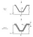
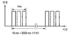
발광부로서의 3개의 LED 소자를 구동하여 터치리스 모션 기능을 실현하는 드라이버를 탑재한 수광 소자가 이미 제공되었다. 도 12a는 배경기술의 터치리스 모션 기능에서의 유저의 손의 좌우측 방향의 움직임의 검출 동작을 설명하는 도면이다. 도 12b는 배경기술의 터치리스 모션 기능에서의 유저의 손의 상하 방향의 움직임의 검출 동작을 설명하는 도면이다. 도 12c는 유저의 손의 좌우측 방향의 움직임에 대한 반사광의 신호 강도를 설명하는 그래프이다. 도 12d는 유저의 손의 상하 방향의 움직임에 대한 반사광의 신호 강도를 설명하는 그래프이다. 도 12e는 각 Ir-LED(101, 102 및 103)의 발광 타이밍을 설명하는 차트이다.A light receiving element equipped with a driver for realizing a touchless motion function by driving three LED elements as a light emitting portion has already been provided. 12A is a view for explaining the motion detection operation in the left and right directions of the user's hand in the touchless motion function of the background art. 12B is a view for explaining the motion detection operation of the user's hand in the up and down direction in the touchless motion function of the background art. 12C is a graph for explaining the signal intensity of the reflected light with respect to the movement in the left and right direction of the user's hand. 12D is a graph for explaining the signal intensity of the reflected light with respect to the vertical movement of the user's hand. 12E is a chart for explaining the light emission timings of the respective Ir-
도 12a에 도시한 바와 같이, 휴대 단말기(100)의 상부이며 휴대 단말기(100)의 하우징 내부에 도 12a의 지면의 가로 방향 및 세로 방향에 대하여 90°의 각도를 형성하도록 3개의 근적외 발광 소자(Ir-LED)(101, 102 및 103)가 배치되어 있다. 또한, 도 12a에 도시한 바와 같이, 휴대 단말기(100)의 상부이며 휴대 단말기(100)의 하우징 내부에 2개의 가로 방향의 Ir-LED(101 및 102) 사이에 수광 소자(105)가 배치되어 있다.12A, in order to form an angle of 90 DEG with respect to the horizontal and vertical directions of the paper of FIG. 12A in the upper portion of the
3개의 Ir-LED(101, 102 및 103)는 도 12e에 도시한 바와 같이 주기 10ms 내지 2000ms의 발광 주기와 가변 발광 타이밍을 갖도록 시분할 방식으로 발광한다. 도 12a 및 도 12c에 도시한 바와 같이 휴대 단말기(100)에 대하여 유저의 손(106)을 우측으로부터 좌측으로 이동시키면, 수광 소자(105)는 우측에 위치하는 2개의 Ir-LED(102 및 103)로부터 시분할 방식으로 발광된 광의 반사광을 수광한다. 수광 소자(105)는, 얼마 있다가, 좌측에 위치하는 다른 Ir-LED(101)로부터의 반사광을 또한 수광한다. 이 수광 타이밍의 편차에 의해 유저의 손(106)의 좌우측 방향의 움직임이 검출된다.The three Ir-
마찬가지로, 도 12c 및 도 12d에 도시한 바와 같이 휴대 단말기(100)에 대하여 유저의 손(106)을 아래로 이동시키면, 수광 소자(105)는 상측에 위치하는 2개의 Ir-LED(101 및 102)로부터 시분할 방식으로 발광된 광의 반사광을 수광한다. 수광 소자(105)는, 얼마 있다가, 하측에 위치하는 다른 Ir-LED(103)로부터의 반사광을 또한 수광한다. 이 수광 타이밍의 편차에 의해 유저의 손(106)의 상하 방향의 움직임이 검출된다.Similarly, when the user's
근접 센서에 관한 선행 기술로서, 기판, 이 기판 상에 열 형상으로 배치된 복수의 수광 소자, 및 각 수광 소자에 대하여 복수개씩 대응해서 설치되도록 열 형상으로 배치된 복수의 발광 소자를 포함하는 수광 및 발광 일체형 소자 어레이가 알려져 있다(예를 들면 특허 문헌 1 참조). 이 수광 및 발광 일체형 소자 어레이는 열 형상으로 설치된 발광 소자로부터의 광에 응답하여 검출 대상 물체로부터의 반사광의 크기(광전류의 크기)에 기초하여, 검출 대상물의 위치를 검출한다.As a prior art relating to a proximity sensor, there is known a proximity sensor including a substrate, a plurality of light receiving elements arranged in a row on the substrate, and a plurality of light receiving elements including a plurality of light emitting elements arranged in a columnar manner so as to correspond to each of the light receiving elements, Emitting element array is known (see, for example, Patent Document 1). The light-receiving and light-emitting element array detects the position of the object to be detected based on the magnitude of reflected light from the object to be detected (the magnitude of the photocurrent) in response to the light from the light-emitting element provided in a columnar form.
그러나, 상기한 배경기술의 근접 센서에는 다음 같은 문제가 있다. 배경기술에서, 휴대 단말기 또는 태블릿 단말기 등의 전자 기기에 터치리스 모션 기능을 탑재할 때 각각의 발광부로서의 예를 들면 Ir-LED를 개별로 기판에 배치하여야 한다. 그러므로, 전자 기기를 조립하는 세트 메이커가 기판을 설계할 때, 세트 메이커는 각 발광부와 수광부 간의 위치 관계를 결정하고 이 결정된 위치 관계에 적합한 발광부의 발광 타이밍(발광 주기)을 조정해야 한다. 따라서, 번거로운 설계를 행해야 한다.However, the proximity sensor of the background art described above has the following problems. In the background art, when a touchless motion function is mounted on an electronic device such as a portable terminal or a tablet terminal, for example, an Ir-LED as each light emitting portion must be individually arranged on a substrate. Therefore, when the set maker for assembling the electronic device designs the substrate, the set maker must determine the positional relationship between each light emitting portion and the light receiving portion and adjust the light emission timing (light emission period) of the light emitting portion suited to the determined positional relationship. Therefore, troublesome design must be performed.
한편, 특허 문헌 1에 기재된 수광 및 발광 일체형 소자 어레이는 소정의 방향(예를 들면, 가로 방향)에서의 검출 대상 물체의 위치를 실제로 검출하지만, 다른 방향(예를 들면, 세로 방향)을 포함하는 방향의 위치를 검출하지 않는다.On the other hand, the light-receiving and light-emitting element array disclosed in
본 발명은 배경기술의 사정을 고려하여 개발되었다. 본 발명의 목적은 미리 발광부의 발광 타이밍을 조정해서 기판의 설계를 간단히 하고 피검출 물체를 고정밀도로 검출할 수 있는 근접 센서를 제공하는 것이다.The present invention has been developed in view of the background art. SUMMARY OF THE INVENTION An object of the present invention is to provide a proximity sensor capable of adjusting a light emission timing of a light emitting portion in advance to simplify the design of a substrate and detecting the object to be detected with high accuracy.
본 발명의 제1 특징의 근접 센서는 피검출 물체를 검출하는 근접 센서로서, 기판; 그 전부가 직선 상에 배열되지 않도록 상기 기판의 표면에 실장되고, 광을 출사하는 적어도 3개의 발광부; 상기 3개의 발광부와 소정의 위치 관계를 갖도록 상기 기판의 표면에 실장되고, 상기 발광부로부터 출사되어 상기 피검출 물체에 의해 반사된 광으로부터 얻어지는 반사광을 수광하는 수광부를 포함하는 근접 센서이다.A proximity sensor according to a first aspect of the present invention is a proximity sensor for detecting an object to be detected, comprising: a substrate; At least three light emitting parts mounted on the surface of the substrate so that all of them are not arranged in a straight line, and emitting light; And a light receiving unit mounted on the surface of the substrate so as to have a predetermined positional relationship with the three light emitting units and receiving reflected light obtained from light emitted from the light emitting unit and reflected by the object to be detected.
본 발명의 제2 특징의 근접 센서에서, 상기 기판은 원샷 레이저 방법에 의해 제조된 3차원 회로 기판이다.In the proximity sensor of the second aspect of the present invention, the substrate is a three-dimensional circuit substrate manufactured by the one-shot laser method.
본 발명의 제3 특징의 근접 센서에서, 상기 적어도 3개의 발광부 및 상기 수광부는 각각 상기 기판의 표면에 형성된 오목부들에 실장된다.In the proximity sensor according to the third aspect of the present invention, the at least three light emitting portions and the light receiving portion are each mounted on the concave portions formed on the surface of the substrate.
본 발명의 제4 특징의 근접 센서에서, 상기 수광부는 상기 적어도 3개의 발광부로부터 출사되어 상기 피검출 물체에 의해 반사된 광으로부터 얻어지는 반사광의 수광 패턴에 기초하여, 상기 피검출 물체의 이동을 검출한다.In the proximity sensor of the fourth aspect of the present invention, the light-receiving unit detects the movement of the object to be detected based on the light-receiving pattern of the reflected light emitted from the light emitted from the at least three light-emitting units and reflected by the object to be detected do.
본 발명의 제5 특징의 근접 센서에서, 상기 적어도 3개의 발광부로부터 출사되는 광의 발광량이 서로 상이하고, 상기 수광부는 상기 반사된 광의 발광량에 기초하여, 상기 표면에 대하여 수직인 방향의 상기 피검출 물체까지의 거리를 검출한다.In the proximity sensor according to the fifth aspect of the present invention, the amounts of light emitted from the at least three light emitting portions are different from each other, and the light receiving portion is configured to detect, based on the amount of light emitted from the at least three light emitting portions, The distance to the object is detected.
본 발명의 제6 특징의 근접 센서에서, 상기 적어도 3개의 발광부가 실장되는 오목부들 각각은 상기 발광부로부터 출사되는 광이 외측을 향하도록, 상기 수광부에 대하여 상기 외측을 향해 변형된 개구부를 갖는다.In the proximity sensor according to the sixth aspect of the present invention, each of the concave portions in which the at least three light emitting portions are mounted has an opening portion deformed toward the outside with respect to the light receiving portion so that light emitted from the light emitting portion faces outward.
본 발명의 제7 특징의 근접 센서에서, 상기 수광부 및 3개의 상기 발광부가 상기 기판의 표면에 사각형의 네 코너에 배치된다.In the proximity sensor of the seventh aspect of the present invention, the light receiving unit and the three light emitting units are arranged at four corners of a square on the surface of the substrate.
본 발명의 제8 특징의 근접 센서에서, 상기 수광부가 상기 기판의 표면의 중앙에 배치되고, 4개의 발광부가 상기 수광부의 주위에 배치된다.In the proximity sensor of the eighth aspect of the present invention, the light receiving portion is disposed at the center of the surface of the substrate, and four light emitting portions are disposed around the light receiving portion.
본 발명에 따르면, 미리 발광부의 발광 타이밍을 조정해서 기판의 설계를 간단히 하고 피검출 물체를 고정밀도로 검출할 수 있다.According to the present invention, the emission timing of the light emitting portion can be adjusted in advance to simplify the design of the substrate, and the object to be detected can be detected with high accuracy.
도 1은 제1 실시예에 따른 근접 센서에서의 발광 소자 및 수광 소자의 배치를 도시하는 도면.
도 2는 제1 실시예에 따른 원샷 레이저 방법에 기초한 3차원 회로 기판의 제조 프로세스의 전반부를, 3차원 회로 기판의 단면도를 이용해서 시계열로 설명하는 도면.
도 3은 제1 실시예에 따른 원샷 레이저 방법에 기초한 3차원 회로 기판의 제조 프로세스의 후반부를, 3차원 회로 기판의 단면도를 이용해서 시계열로 설명하는 도면.
도 4는 금형 A와 금형 B를 이용해서 수지 기판을 형성하는 상태를 도시하는 도면.
도 5a 및 5b는 3차원 회로 기판에 발광 소자 및 수광 소자가 실장된 근접 센서의 단면 구조를 도시하는 단면도로, 도 5a는 도 1의 화살표 A-A선 방향으로부터 본 단면 구조를 도시하는 단면도이고, 도 5b는 도 1의 화살표 B-B선 방향으로부터 본 단면 구조를 도시하는 단면도.
도 6a 및 6b는 터치리스 모션의 검출시에 근접 센서 내의 수광 소자에 의해 검출된 검출 신호를 도시하는 타이밍 차트로, 도 6a는 피검출 물체가 도 1에 도시하는 근접 센서의 하측으로부터 상측으로 이동하는 경우를 도시하고, 도 6b는 피검출 물체가 도 1에 도시하는 근접 센서의 상측으로부터 하측으로 이동하는 경우를 도시한다.
도 7a 및 7b는 터치리스 모션의 검출시에 근접 센서 내의 수광 소자에 의해 검출된 검출 신호를 도시하는 타이밍 차트로, 도 7a는 피검출 물체가 도 1에 도시하는 근접 센서의 우측으로부터 좌측으로 이동하는 경우를 도시하고, 도 7b는 피검출 물체가 도 1에 도시하는 근접 센서의 좌측으로부터 우측으로 이동하는 경우를 도시한다.
도 8은 제2 실시예에 따른 근접 센서에서의 발광 소자 및 수광 소자의 배치를 도시하는 도면.
도 9a 및 9b는 피검출 물체까지의 거리에 대한 수광 소자의 검출 신호의 변화를 도시하는 그래프로, 도 9a는 수광 소자의 검출 신호의 예를 도시하는 그래프이고, 도 9b는 수광 소자의 검출 신호의 다른 예를 도시하는 그래프.
도 10a 내지 10c는 제3 실시예에 따른 근접 센서에서의 복수의 발광 소자가 각각 실장되는 3차원 회로 기판의 복수의 오목부의 형상, 및 각 발광 소자로부터 출사되는 광의 출사 방향을 도시하는 도면으로, 도 10a는 근접 센서의 평면도이고, 도 10b는 도 10a의 화살표 C-C선 방향으로부터 본 단면도이고, 도 10c는 제3 실시예의 변형예에 따른 근접 센서의 평면도.
도 11a 및 11b는 제4 실시예에 따른 근접 센서에서의 발광 소자 및 수광 소자의 배치를 도시하는 도면으로, 도 11a는 근접 센서의 평면도이고, 도 11b는 제4 실시예의 변형예에 따른 근접 센서의 평면도.
도 12a는 배경기술의 터치리스 모션 기능에서의 유저의 손의 수평 움직임의 검출 동작을 설명하는 도면이고, 도 12b는 배경기술의 터치리스 모션 기능에서의 유저의 손의 수직 움직임의 검출 동작을 설명하는 도면이고, 도 12c는 유저의 손의 수평 움직임에 대한 반사광의 신호 강도를 설명하는 그래프이고, 도 12d는 유저의 손의 수직 움직임에 대한 반사광의 신호 강도를 설명하는 그래프이고, 도 12e는 각 Ir-LED의 발광 타이밍을 설명하는 차트.BRIEF DESCRIPTION OF THE DRAWINGS Fig. 1 is a diagram showing the arrangement of a light emitting element and a light receiving element in a proximity sensor according to the first embodiment; Fig.
Fig. 2 is a diagram for explaining the first half of a manufacturing process of a three-dimensional circuit board based on the one-shot laser method according to the first embodiment in time series using a sectional view of a three-dimensional circuit board.
3 is a time-series explanatory diagram of a second half of a process for manufacturing a three-dimensional circuit board based on the one-shot laser method according to the first embodiment, using a sectional view of the three-dimensional circuit board.
4 is a view showing a state in which a resin substrate is formed using the molds A and B;
5A and 5B are cross-sectional views showing a cross-sectional structure of a proximity sensor in which a light emitting element and a light receiving element are mounted on a three-dimensional circuit board, FIG. 5A is a cross- 5B is a sectional view showing the sectional structure viewed from the direction of arrow BB in Fig.
6A and 6B are timing charts showing a detection signal detected by a light receiving element in the proximity sensor when touchless motion is detected. FIG. 6A is a timing chart in which the object to be detected moves from the lower side to the upper side And Fig. 6B shows a case where the object to be detected moves from the upper side to the lower side of the proximity sensor shown in Fig.
7A and 7B are timing charts showing detection signals detected by the light receiving elements in the proximity sensor at the time of detection of the touchless motion, and Fig. 7A is a timing chart in which the object to be detected moves from the right side to the left side Fig. 7B shows a case where the object to be detected moves from the left side to the right side of the proximity sensor shown in Fig. 1. Fig.
8 is a diagram showing the arrangement of a light emitting element and a light receiving element in the proximity sensor according to the second embodiment;
9A is a graph showing an example of a detection signal of a light receiving element, and FIG. 9B is a graph showing an example of a detection signal of the light receiving element. FIG. 9A is a graph showing a change in the detection signal of the light receiving element with respect to the distance to the object to be detected, Fig.
10A to 10C are views showing the shapes of a plurality of concave portions of a three-dimensional circuit board on which a plurality of light emitting elements in the proximity sensor according to the third embodiment are respectively mounted and the emitting direction of light emitted from each light emitting element, FIG. 10A is a plan view of the proximity sensor, FIG. 10B is a cross-sectional view taken along arrow CC in FIG. 10A, and FIG. 10C is a plan view of a proximity sensor according to a modification of the third embodiment.
11A and 11B are diagrams showing the arrangement of the light emitting element and the light receiving element in the proximity sensor according to the fourth embodiment. Fig. 11A is a plan view of the proximity sensor, FIG.
Fig. 12A is a view for explaining the detection operation of the horizontal movement of the user's hand in the touchless motion function of the background art, Fig. 12B is a view for explaining the detection operation of vertical movement of the user's hand in the touchless motion function of the background art 12D is a graph for explaining the signal intensity of the reflected light with respect to the vertical movement of the user's hand, and FIG. 12E is a graph illustrating the signal intensity of the reflected light with respect to the horizontal movement of the user's hand. A chart explaining the emission timing of the Ir-LED.
본 발명의 근접 센서의 각 실시예에 대해서 도면을 참조하여 설명한다.Each embodiment of the proximity sensor of the present invention will be described with reference to the drawings.
본 실시 형태의 근접 센서는 휴대 단말기 또는 태블릿 단말기 등의 전자 기기의 하우징 내부에 설치되어 유저의 손 또는 손가락 등의 피검출 물체를 검출한다.The proximity sensor of the present embodiment is installed inside a housing of an electronic device such as a portable terminal or a tablet terminal to detect an object to be detected such as a hand or a finger of a user.
(제1 실시예)(Embodiment 1)
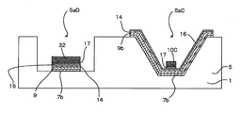
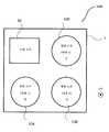
도 1은 제1 실시예에 따른 근접 센서(19)에서의 발광 소자 및 수광 소자의 배치를 도시하는 도면이다. 근접 센서(19)는 3차원 회로 기판(1)의 상면에 적어도 3개의 발광 소자(10A, 10B 및 10C)와 1개의 수광 소자(32)가 실장되어 구성되어 있다. 도 1에 도시한 바와 같이, 3차원 회로 기판(1)의 상면의 사각형의 네 코너에 3개의 발광 소자(10A, 10B 및 10C)와 수광 소자(32)가 배치되어 있다. 즉, 3차원 회로 기판(1)은 각 발광 소자(10A, 10B 및 10C)의 전기 회로가 실장되는, 예를 들면 원형의 저부(저면)와 이 저부(저면)의 주위를 둘러싸는 벽면으로 형성된 원형의 오목부(도시 생략), 및 수광 소자(32)의 전기 회로가 실장되는, 예를 들면 사각형의 저부(저면)와 이 저부(저면)의 주위를 둘러싸는 벽면으로 형성된 사각형의 오목부(도시 생략)를 포함하는 구성을 갖는다.1 is a diagram showing the arrangement of a light emitting element and a light receiving element in the
발광부로서의 발광 소자(10A, 10B 및 10C)는, 구동 전류가 공급되면, (발광 1), (발광 2) 및 (발광 3)의 순서로 시분할 방식으로 적외선(예를 들면, 근적외선)을 발하는 Ir-LED를 포함한다.The
수광부로서의 수광 소자(32)는 포토다이오드와 이 포토다이오드를 구동하기 위한 드라이버 회로를 포함하는 구성을 갖는다. 이 드라이버 회로는, 후술하는 바와 같이, 터치리스 모션 기능 및 피검출 물체까지의 거리를 검출하는 기능을 갖는다.The light-receiving
또한, MID 기술을 이용하는 제조 프로세스에 의해 제조된 3차원 회로 기판(1)에 발광 소자(10A, 10B 및 10C) 및 수광 소자(32)가 실장된다(도 4 참조). 이렇게 근접 센서(19)가 제조된다.Further, the
도 2는 제1 실시예에 따른 원샷 레이저 방법(원샷 레이저 윤곽 제거 방법)에 기초한 3차원 회로 기판의 제조 프로세스의 전반부를, 3차원 회로 기판의 단면도를 이용해서 시계열로 설명하는 도면이다. 도 3은 제1 실시예에 따른 원샷 레이저 방법에 기초한 3차원 회로 기판의 제조 프로세스의 후반부를, 3차원 회로 기판의 단면도를 이용해서 시계열로 설명하는 도면이다.2 is a diagram for explaining the first half of a manufacturing process of a three-dimensional circuit board based on the one-shot laser method (one-shot laser contour removal method) according to the first embodiment in a time series using a sectional view of a three-dimensional circuit board. Fig. 3 is a diagram for explaining the second half of the manufacturing process of a three-dimensional circuit board based on the one-shot laser method according to the first embodiment in a time series using a sectional view of the three-dimensional circuit board.
원샷 레이저 방법은 사출 성형을 한번 행하고, 사출 성형에 의해 제조된 기판 상에 원하는 전기 회로가 실장되는 회로 패턴의 주위의 윤곽을 레이저 광으로 조사하여 원하는 금속 층 또는 막을 형성시켜서 3차원 회로 기판을 제조하는 방법이다.The one-shot laser method is a method in which a three-dimensional circuit board is manufactured by performing injection molding once, irradiating a contour of a circuit pattern on which a desired electric circuit is mounted on a substrate manufactured by injection molding with laser light to form a desired metal layer or film .
도 2 및 도 3에서, 3차원 회로 기판(1)의 제조 프로세스의 설명을 간단히 하기 위해서, 도 1에 도시하는 발광 소자(10A, 10B 및 10C) 및 수광 소자(32)가 일체로 실장되는 3차원 회로 기판(1)의 제조 프로세스를, 예를 들면 발광 소자(10A)에 주목하여 설명한다. 도 2 및 도 3의 설명은 도 1에 도시하는 발광 소자(10A, 10B 및 10C) 및 수광 소자(32)가 일체로 실장되는 3차원 회로 기판(1)의 제조 프로세스에 적용가능하다.2 and 3, in order to simplify the description of the manufacturing process of the three-
원샷 레이저 방법에 기초한 3차원 회로 기판의 제조 프로세스(제조 방법)는 이하의 (공정 1) 내지 (공정 6)의 프로세스 순서에 따라 행해진다.The manufacturing process (manufacturing method) of the three-dimensional circuit substrate based on the one-shot laser method is performed according to the following process sequence of (process 1) to (process 6).
(공정 1) 1차 성형의 프로세스에서, 사출 성형기에, 예를 들면 발광 소자(10A)가 실장되는 3차원 회로 기판(1)의 각 오목부의 형상에 대응하는 금형을 형성하도록 금형 A와 금형 B가 설치된다. 금형 A와 금형 B 사이의 공간에 도금가능한 수지 재료가 주입된다. 수지 재료에는, 예를 들면 폴리프탈아미드(PPA), 알루미나(Al2O3) 및 질화 알루미늄(AlN)이 이용된다. (공정 1)의 프로세스는 본 실시예에 따른 3차원 회로 기판(1)을 준비하는 공정이다. 동 프로세스에서, 본 실시예에 따른 3차원 회로 기판(1)의 기초(1차 성형 물품)로서의 수지 기판(5)이 성형된다. 또한, 준비 공정은 (공정 1)의 1차 성형의 프로세스에서 수지 기판(5)을 사출 성형하는 공정으로 한정되지 않는다. 예를 들면, 준비 공정은 제삼자(제조 위탁자 등)로부터 구입한 수지 기판(5)을 이용하는 공정을 포함할 수 있다. 도 2에 도시한 바와 같이, 수지 기판(5)에 금형 A 및 금형 B의 형상에 대응하여 절구형(conical) 오목부(5a)가 형성된다.(Process 1) In the process of the primary molding, a mold A and a mold B (not shown) are formed in the injection molding machine so as to form a mold corresponding to the shape of each recess of the three-
도 4는 금형 A와 금형 B를 이용해서 수지 기판(5)을 형성하는 상태를 도시하는 도면이다. 금형 A에는 수지 기판(5)의 오목부(5a)에 맞닿는 볼록부(11a)가 형성되어 있다. 이 볼록부(11a)의 선단면(11b)은 미리 평탄한 면으로 연마되어 있고, 볼록부(11a)의 측면(11c)도 미리 평활한 면 또는 곡면으로 연마되어 있다.4 is a diagram showing a state in which the
(공정 1)의 프로세스에서, 미리 연마된 선단면(11b) 및 측면(11c)을 포함하는 금형 A를 이용함으로써 사출 성형된 수지 기판(5)의 오목부(5a)에 저부로서의 평활한 저면(5b) 및 평활한 벽면(5c)을 형성할 수 있다.(Step 1), the
(공정 1)의 프로세스에서, 사출 성형된 수지 기판(5)의 오목부(5a)에 평활한 저면(5b) 및 곡면적으로 매끄러운 벽면(5c)이 형성될 수 있다. (공정 1)의 프로세스와 (공정 2)의 프로세스 사이에서 1차 성형 물품으로서의 수지 기판(5)에 대하여 플라스마 처리되는 것이 바람직하다. 결과적으로, 수지 기판(5)의 표면이 활성화될 수 있다.A
(공정 2) 1차 성형의 프로세스의 다음의 메탈라이징의 프로세스에서, 수지 기판(5)의 표면 또는 전체 면에 스퍼터링에 의해 예를 들면 Cu 박막(구리 박막)(7)이 형성된다. (공정 2)의 프로세스에서, 수지 기판(5)의 표면 또는 전체 면에 형성되는 Cu 박막(7)의 두께는 예를 들면, 0.3μm이다. (공정 1)의 프로세스에서 연마된 금형 A가 이용되기 때문에, 수지 기판(5)의 오목부(5a)의 표면(저면(5b) 및 벽면(5c))은 평활하게 형성된다. 따라서, (공정 2)의 프로세스에서 수지 기판(5)의 표면에 형성된 Cu 박막(7)도 또한 평활하게 형성된다.(Process 2) In the following metallization process of the primary molding process, for example, a Cu thin film (copper thin film) 7 is formed on the surface or the entire surface of the
(공정 3) 메탈라이징의 프로세스의 다음의 레이저 패터닝의 프로세스에서, 원하는 발광 소자(10A)의 전기 회로가 실장되는 회로 패턴을 형성하는 개소를 포함하는 소정 범위 내의 윤곽(8)의 부분이 레이저 광에 의해 Cu 박막(7)으로부터 제거된다. 이 소정 범위는 수지 기판(5)의 오목부(5a)의 좌측 표면의 일부로부터 오목부(5a)의 좌측의 벽면(5c), 저면(5b), 오목부(5a)의 우측의 벽면(5c), 및 수지 기판(5)의 우측 표면의 일부(도시 생략)에까지 미친다(도 2의 (공정 3) 참조).(Process 3) In the process of laser patterning next to the metallization process, a portion of the contour 8 within a predetermined range including a portion forming a circuit pattern on which the electric circuit of the desired
또한, 도 2는 발광 소자(10A)에 주목한 제조 프로세스를 도시한다. 도 2에는 상세하게 도시하지는 않았지만, 본 실시예에 따른 3차원 회로 기판(1)에서는 그리고 도 2의 3차원 회로 기판(1)의 우측에는 발광 소자(10B)의 전기 회로가 실장되는 오목부가 마찬가지로 형성되어 있다. 전술한 소정 범위의 우측 단부는 발광 소자(10B)의 전기 회로가 실장되는 오목부(도시 생략)의 좌측 표면의 일부에 대응한다. 결과적으로, 수지 기판(5)의 저면(5b)에는 전술한 소정 범위 내의 윤곽(8)의 부분이 제거된 Cu 박막(7b)이 남고, 수지 기판(5)의 측면 및 배면에는 Cu 박막(7d)이 남는다.2 shows a manufacturing process paying attention to the
(공정 4) 레이저 패터닝의 프로세스의 다음의 전해 Cu 도금의 프로세스에서, 원하는 발광 소자(10A)의 전기 회로가 실장되는 급전 부분을 포함하는 소정 범위(전술한 범위 참조)에 전해 Cu(구리) 도금이 행해진다. 이 전해 Cu 도금에 의해, 원하는 발광 소자의 전기 회로가 실장되는 급전 부분을 포함하는 소정 범위 내의 윤곽(8)의 부분에 의해 둘러싸여진 Cu 박막(7b)에 Cu 도금층(9b)이 두껍게 도포된다. 즉, 소정의 두께를 갖는 Cu 도금층(9b)이 형성된다(도 2의 (공정 4) 참조). (공정 4)의 프로세스에서, Cu 도금층(9)의 두께는 12μm이다.(Process 4) In the process of electrolytic Cu plating subsequent to the process of laser patterning, electrolytic Cu (copper) plating is performed in a predetermined range (see the above-mentioned range) including a power feeding portion where the electric circuit of the desired
(공정 1)의 프로세스에서 연마된 금형이 이용되기 때문에, Cu 도금층(9b)의 기초 부분이 되는 수지 기판(5)의 성형 면 및 나아가 이 성형 면 상에 형성된 Cu 박막(7b)의 표면이 평활하다. 따라서, Cu 도금층(9b)의 두께는 비교적 얇을 수 있다.The forming surface of the
(공정 5) 전해 Cu 도금의 프로세스의 다음의 에칭의 프로세스에서, 전해 Cu 도금의 지난 프로세스에서 Cu 도금층(9b)이 형성된 수지 기판(5)에 대하여 등방성또는 이방성의 에칭이 행해진다. (공정 5)의 에칭에 의해, Cu 도금층(9b)의 표면은, 예를 들면 두께 2μm 정도로 균일하게 용융된다. 따라서, Cu 도금층(9b)의 표면은 평활해진다. 결과적으로, Cu 도금층(9b)의 두께는 10μm가 된다.(Step 5) In the next etching process of the electrolytic Cu plating process, isotropic or anisotropic etching is performed on the
(공정 5)의 에칭의 프로세스에서, Cu 도금층(9b) 이외에 수지 기판(5)의 표면의 일부, 측면 및 배면에 형성되어 있는 Cu 박막(7d)에 대하여도 에칭이 행해진다. 따라서, 수지 기판(5)의 표면의 일부, 측면 및 배면에 형성되어 있는 Cu 박막(7)이 에칭된다.Etching is also performed on the Cu
(공정 6) 최후에, 에칭의 프로세스의 다음의 전해 Ni-Au 도금의 프로세스에서, 전해 도금에 의해 니켈(Ni)의 도금층이 형성되고 마찬가지로 니켈(Ni)의 도금층 위에 금(Au)의 도금층이 더욱 형성된다.(Step 6) Finally, in the electrolytic Ni-Au plating process subsequent to the etching process, a plating layer of nickel (Ni) is formed by electrolytic plating, and a plating layer of gold (Au) is formed on the plating layer of nickel Respectively.
보다 구체적으로, 원하는 발광 소자(10A)의 전기 회로가 실장되는 급전 부분을 포함하는 소정 범위 내에 형성된 Cu 도금층(9b)에 대하여 와트욕(Watts bath)으로 전해 Ni 도금이 행해진다. 결과적으로, Cu 도금층(9b) 위에 Ni 도금층(14)이 형성된다(도 3의 (공정 6) 참조). (공정 6)의 프로세스에서, 와트욕을 이용하여 수지 기판(5)의 오목부(5a)의 저면(5b) 및 벽면(5c) 각각에 Ni 도금층(14)을 형성하여, 매우 높은 광택성을 실현할 수 있고, 이들 면을 평탄하고 평활하게 할 수 있다. 또한, 전술한 바와 같이 벽면(5c)은 평탄하지 않고 곡면일 수도 있다.More specifically, electrolytic Ni plating is performed on the
또한, (공정 6)의 프로세스에서, Ni 도금층(14)에 대하여 전해 Au 도금이 행해진다. 결과적으로, 수지 기판(5)의 오목부(5a)의 저면(5b) 및 벽면(5c) 위에 형성된 각 Ni 도금층(14) 위에 Au 도금층(16)(금막)이 더욱 형성된다.Further, in the process of (Step 6), electrolytic Au plating is performed on the
도 2 및 도 3에 도시한 원샷 레이저 방법에 의해, 본 실시예에 따른 3차원 회로 기판(1)에서, 원하는 발광 소자(10A)의 전기 회로가 실장되는 급전 부분을 포함하는 소정 범위 내에 Cu 박막(7b), Cu 도금층(9b), Ni 도금층(14) 및 Au 도금층(16)이 순차적으로 형성된다. 따라서, 본 실시예에 따른 3차원 회로 기판(1)에서, 발광 소자(10A)로부터의 광을 반사하기 위한 반사면으로서 설치된 수지 기판(5)의 벽면(5c) 위에 Cu 박막(7b), Cu 도금층(9b), Ni 도금층(14) 및 Au 도금층(16)이 순차적으로 형성된다.2 and 3, in the three-
이와 같은 프로세스에 의해 원샷 레이저 방법에 의한 3차원 회로 기판(1)이 제조된다. 또한, Cu 박막(7b)의 두께, 전해 도금에 의해 두껍게 도포된 Cu 도금층(9b)의 두께, 및 에칭 후의 Cu 도금층(9b)의 두께는 일례이다. 이들 두께는 이들 수치에 한정되지 않는다.The three-
도 5a 및 5b는 3차원 회로 기판(1)에 발광 소자(10A, 10B 및 10C) 및 수광 소자(32)가 실장된 근접 센서(19)의 단면 구조를 도시하는 단면도이다. 도 5a는 도 1의 화살표 A-A선 방향으로부터 본 단면 구조를 도시한다. 도 5b는 도 1의 화살표 B-B선 방향으로부터 본 단면 구조를 도시한다.5A and 5B are sectional views showing a sectional structure of a
오목부(5aA, 5aB 및 5aC)에는 각각 발광 소자(10A, 10B 및 10C)가 실장(배치)되고, 오목부(5aD)에는 수광 소자(32)가 실장된다. 이하의 설명에서, 오목부(5aA, 5aB 및 5aC)를 서로 구별할 필요가 없을 경우에는 간단히 오목부(5a)라고 칭한다.The
각 발광 소자(10A, 10B 및 10C)는 Au 도금층(16) 위에 실장되고, 발광 소자(10A, 10B 및 10C)와 Au 도금층(16)은 접착제(17)를 통해 서로 고정된다. 발광 소자(10A, 10B 및 10C)로부터 출사되는 광은 직접적으로 출사되거나 또는 대응하는 오목부(5aA, 5aB 및 5aC)의 벽면에 형성된 반사면에서 정반사된다. 따라서, 이 광은 확산을 억제하면서 전방(도 5a 및 5b 중 상방)으로 출사된다. 이 출사된 광이 유저의 손가락 또는 손 등의 피검출 물체에 의해 반사될 때, 반사광의 일부가 수광 소자(32)에 입사하고 수광 소자(32)에 의해 검출된다.Each of the
본 실시예에서, 3개의 발광 소자(10A, 10B 및 10C)는 미리 설정된 발광 타이밍(예를 들면, 200[msec]의 발광 주기)에서 시분할 방식으로 발광하도록 설정되어 있다. 또한, 3개의 발광 소자(10A, 10B 및 10C)는 동시에 발광하지 않고 광의 간섭을 피하기 위해, 예를 들면 1[msec]의 범위 내에서, 서로 시간적으로 어긋나게 해서 순차적으로 발광하는 것이 바람직하다.In this embodiment, the three
도 6a 및 6b는 터치리스 모션의 검출시에 근접 센서(19) 내의 수광 소자(32)에 의해 검출된 검출 신호를 도시하는 타이밍 차트이다. 종축은 검출 신호의 크기를 나타내고, 횡축은 시간을 나타낸다. 도 6a는 피검출 물체가 근접 센서(19)의 하측으로부터 상측으로 이동하는 경우를 나타낸다.6A and 6B are timing charts showing detection signals detected by the light-receiving
우선, 피검출 물체가 도 1에 도시하는 근접 센서(19)의 하측으로부터 상측으로 이동하는 경우, 수광 소자(32)는 각 발광 소자(10A 및 10B)로부터 출사된 광이 피검출 물체에 의해 반사되어 얻어지는 반사광을 검출하고, 검출 신호(1 및 2)를 출력한다. 검출 신호(1, 2 및 3)는 발광 소자(10A, 10B 및 10C)로부터 출사되는 광의 순서, 즉 (발광 1), (발광 2) 및 (발광 3)의 순서에 대응한다. 또한, 검출 신호(1, 2 및 3)는 수광 소자(32)에 내장된 드라이버 회로가 수광 소자(32)의 광전 변환에 의해 생긴 전기 에너지에 기초하여 생성해서 출력한 신호이다.First, when the object to be detected moves from the lower side to the upper side of the
도 6a에 도시한 바와 같이, 피검출 물체가 발광 소자(10A 및 10B)의 상방(도 1의 지면의 표면 방향, 이하의 설명에서 동일하게 적용됨)의 부분을 차단하도록 위치할 때 발광 소자(10A 및 10B)로부터의 광을 이 피검출 물체가 반사하고 있는 한, 검출 신호(1 및 2)는 전술한 발광 주기마다 출력된다.As shown in Fig. 6A, when the object to be detected is positioned so as to block the portion above the
피검출 물체가 발광 소자(10A 및 10B)의 상방을 통과하고 피검출 물체가 발광 소자(10C)를 차단하는 위치에 도달하면, 수광 소자(32)는 발광 소자(10C)로부터 출사된 광이 피검출 물체에 의해 반사되어 얻어지는 반사광을 검출하고, 검출 신호(3)를 출력한다.When the object to be detected passes above the
수광 소자(32)에 내장된 드라이버 회로는 검출 신호(1, 2 및 3)의 이러한 출력 패턴(수광 패턴)에 기초하여, 피검출 물체가 도 1에 도시하는 근접 센서(19)의 하측으로부터 상측으로 이동했다고 판단할 수 있다.The driver circuit built in the
도 6b는 피검출 물체가 도 1에 도시하는 근접 센서(19)의 상측으로부터 하측으로 이동하는 경우를 도시한다. 마찬가지로, 피검출 물체가 도 1에 도시하는 근접 센서(19)의 하측으로부터 상측으로 이동하는 경우, 수광 소자(32)는 발광 소자(10C)로부터 출사된 광이 피검출 물체에 의해 반사되어 얻어지는 반사광을 검출하고, 검출 신호(3)를 출력한다.6B shows a case where the object to be detected moves from the upper side to the lower side of the
도 6b에 도시한 바와 같이, 피검출 물체가 발광 소자(10C)의 상방의 부분을 차단하도록 위치할 때 발광 소자(10C)로부터의 광을 이 피검출 물체가 반사하고 있는 한, 검출 신호(3)는 전술한 발광 주기마다 출력된다.As long as the object to be detected reflects the light from the light emitting element 10C when the object to be detected is positioned so as to block the portion above the light emitting element 10C as shown in Fig. Is output every light emission period described above.
피검출 물체가 발광 소자(10C)의 상방을 통과하고 피검출 물체가 발광 소자(10A 및 10B)를 차단하는 위치에 도달하면, 수광 소자(32)는 발광 소자(10A 및 10B)로부터 각각 출사된 광이 피검출 물체에 의해 반사되어 얻어지는 반사광을 검출하고, 검출 신호(1 및 2)를 출력한다.When the object to be detected passes above the light emitting element 10C and the object to be detected reaches a position where it blocks the
수광 소자(32)에 내장된 드라이버 회로는 검출 신호(1, 2 및 3)의 이러한 출력 패턴(수광 패턴)에 기초하여, 피검출 물체가 도 1에 도시하는 근접 센서(19)의 상측으로부터 하측으로 이동했다고 판단할 수 있다.The driver circuit built in the
피검출 물체가 수직으로 이동하는 경우뿐만 아니라 수평으로 이동하는 경우에도, 마찬가지로, 검출 신호(1, 2 및 3)의 출력 패턴(수광 패턴)에 기초하여 피검출 물체의 이동 방향을 판단할 수 있다(도 7a 및 7b 참조). 도 7a 및 7b는 터치리스 모션의 검출시에 근접 센서 내의 수광 소자에 의해 검출된 검출 신호를 도시하는 타이밍 차트이다. 도 7a는 피검출 물체가 도 1에 도시하는 근접 센서의 우측으로부터 좌측으로 이동하는 경우를 도시한다. 도 7b는 피검출 물체가 도 1에 도시하는 근접 센서의 좌측으로부터 우측으로 이동하는 경우를 도시한다.The moving direction of the object to be detected can be determined based on the output pattern (light-receiving pattern) of the detection signals 1, 2, and 3 in the same manner, not only when the object to be detected moves vertically but also when it moves horizontally (See Figs. 7A and 7B). 7A and 7B are timing charts showing detection signals detected by the light-receiving elements in the proximity sensor at the time of detection of the touchless motion. 7A shows a case where the object to be detected moves from the right side to the left side of the proximity sensor shown in Fig. Fig. 7B shows a case where the object to be detected moves from the left side to the right side of the proximity sensor shown in Fig.
피검출 물체가 도 1에 도시하는 근접 센서(19)의 우측으로부터 좌측으로 이동하는 경우, 수광 소자(32)는 발광 소자(10B 및 10C)로부터 출사된 광이 피검출 물체에 의해 반사되어 얻어지는 반사광을 검출하고, 검출 신호(2 및 3)를 출력한다.When the object to be detected moves from the right side to the left side of the
도 7a에 도시한 바와 같이, 피검출 물체가 발광 소자(10B 및 10C)의 상방을 차단하도록 위치할 때 발광 소자(10B 및 10C)로부터의 광을 이 피검출 물체가 반사하고 있는 한, 검출 신호(2 및 3)는 전술한 발광 주기마다 출력된다.As long as the object to be detected reflects the light from the
피검출 물체가 발광 소자(10B 및 10C)의 상방을 통과하고 발광 소자(10A)를 차단하는 위치에 도달하면, 수광 소자(32)는 발광 소자(10A)로부터 출사된 광이 피검출 물체에 의해 반사되어 얻어지는 반사광을 검출하고, 검출 신호(1)를 출력한다.When the object to be detected reaches the position where it passes above the
수광 소자(32)에 내장된 드라이버 회로는 검출 신호(1, 2 및 3)의 이러한 출력 패턴(수광 패턴)에 기초하여 피검출 물체가 도 1에 도시하는 근접 센서(19)의 우측으로부터 좌측으로 이동했다고 판단할 수 있다.The driver circuit built in the
또한, 피검출 물체가 도 1에 도시하는 근접 센서(19)의 좌측으로부터 우측으로 이동하는 경우, 수광 소자(32)는 발광 소자(10A)로부터 출사된 광이 피검출 물체에 의해 반사되어 얻어지는 반사광을 검출하고, 검출 신호(1)를 출력한다.When the object to be detected moves from the left side to the right side of the
도 7b에 도시한 바와 같이, 피검출 물체가 발광 소자(10A)의 상방의 부분을 차단하도록 위치할 때 발광 소자(10A)로부터의 광을 이 피검출 물체가 반사하고 있는 한, 검출 신호(1)는 전술한 발광 주기마다 출력된다.As long as the object to be detected reflects the light from the
피검출 물체가 발광 소자(10A)의 상방을 통과하고 발광 소자(10B 및 10C)를 차단하는 위치에 도달하면, 수광 소자(32)는 발광 소자(10B 및 10C)로부터 출사된 광이 피검출 물체에 의해 반사되어 얻어지는 반사광을 검출하고, 검출 신호(2 및 3)를 출력한다.When the object to be detected reaches the position where it passes above the
수광 소자(32)에 내장된 드라이버 회로는 검출 신호(1, 2 및 3)의 이러한 출력 패턴(수광 패턴)에 기초하여 피검출 물체가 도 1에 도시하는 근접 센서(19)의 좌측으로부터 우측으로 이동했다고 판단할 수 있다.The driver circuit built in the
더 상세한 설명은 생략하지만, 수광 소자(32)에 내장된 드라이버 회로는 피검출 물체가 도 1에 도시하는 근접 센서(19)의 예를 들면 좌상측으로부터 우하측으로 경사 45°방향으로 이동하는 경우에도, 마찬가지로 피검출 물체의 이동 방향을 판단할 수 있다.Although not described in detail, the driver circuit built in the light-receiving
본 실시예에서는 발광 소자(10A, 10B 및 10C)에 공급되는 구동 전류값은 서로 동일한 값으로 설정되어 있으므로, 발광 소자(10A, 10B 및 10C)로부터 출사된 광을 수광 소자(32)가 검출해서 출력하는 검출 신호의 크기는 거의 동일하다.Since the drive current values supplied to the
이와 같이, 제1 실시예에 따른 근접 센서(19)에 따르면, 근접 센서(19)를 구성하는 발광 소자(10A, 10B 및 10C) 및 수광 소자(32)를 1개의 3차원 회로 기판(1) 위에 실장함으로써 하나로 패키지화할 수 있다. 따라서, 근접 센서(19)의 제조 과정에서, 3개의 발광 소자 간의 위치 관계가 고정되어 3개의 발광 소자의 위치 결정을 고정밀도로 실현할 수 있다. 그러므로, 미리 발광부의 발광 타이밍을 조정해서 기판의 설계를 간단히 하고, 피검출 물체를 고정밀도로 검출할 수 있다.As described above, according to the
또한, 원샷 레이저 방법을 이용해서 3차원 회로 기판(1)이 제조되므로, 고기능화, 박형화 및 경량화를 달성할 수 있다.In addition, since the three-
또한, 3개의 발광 소자와 1개의 수광 소자가 3차원 회로 기판(1)의 오목부들에 실장되므로, 위치 관계의 고정이 용이해진다.In addition, since the three light emitting elements and the one light receiving element are mounted on the recesses of the three-
또한, 3개의 발광 소자(10A, 10B 및 10C)와 1개의 수광 소자(32)가 소정의 위치 관계, 즉, 여기서는 사각형의 네 코너에 배치되어 있으므로, 조밀한 구성으로 될 수 있고, 터치리스 모션의 검출 시 수직 및 수평 검출이 용이해진다. 또한, 임의의 소정의 위치 관계가 이들 소자가 직선으로 배열되는 경우에 이용될 수 있다. 소자들은 임의로 배치될 수 있다.Further, since the three light emitting
(제2 실시예)(Second Embodiment)
제1 실시예는 근접 센서가 조립되어 있는 전자 기기의 디스플레이의 표면을 따라 손 또는 손가락 등의 피검출 물체를 이동시키는 터치리스 모션을 검출할 수 있는 근접 센서를 나타냈다. 제2 실시예는 터치리스 모션을 검출할 수 있을 뿐만 아니라 근접 센서가 조립되어 있는 전자 기기의 디스플레이의 표면으로부터 수직 방향(Z축 방향)에 있는 피검출 물체까지의 거리를 검출할 수 있는 근접 센서를 나타낸다.The first embodiment shows a proximity sensor capable of detecting a touchless motion that moves a subject such as a hand or a finger along a surface of a display of an electronic device in which a proximity sensor is assembled. The second embodiment is a proximity sensor capable of detecting touchless motion as well as detecting the distance from the surface of the display of the electronic device in which the proximity sensor is assembled to the object to be detected in the vertical direction (Z-axis direction) .
도 8은 제2 실시예에 따른 근접 센서(19A)에서의 발광 소자(10A, 10B 및 10C) 및 수광 소자(32)의 배치를 도시하는 도면이다. 제2 실시예에 따른 근접 센서(19A)는 제1 실시예에 따른 근접 센서(19)와 거의 동일한 구성을 갖는다. 그러므로, 제1 실시예와 동일한 구성 요소는 동일한 부호가 참조된다.8 is a diagram showing the arrangement of the
제2 실시예에 따른 근접 센서(19A)에서, 3개의 발광 소자(10A, 10B 및 10C)로부터 출사되는 근적외선의 광량(강도)이 서로 상이하다. 즉, 발광 소자(10A, 10B 및 10C)의 발광량은 각각 "약", "강" 및 "중"이다.In the
따라서, 발광 소자(10B)로부터 출사되는 근적외선이 가장 먼 거리(원거리)까지 닿고, 발광 소자(10C)로부터 출사되는 근적외선이 중거리까지 닿고, 발광 소자(10A)로부터 출사되는 근적외선은 근거리까지만 닿는다. 본 실시예에서, 각 발광 소자(10A, 10B 및 10C)로부터 출사된 광량을 각 발광 소자(10A, 10B 및 10C)에 공급되는 구동 전류의 크기에 따라 가변시킨다.Therefore, the near-infrared rays emitted from the
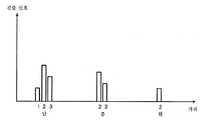
도 9a 및 9b는 피검출 물체까지의 거리에 대한 수광 소자(32)의 검출 신호의 변화를 도시하는 그래프이다. 도 9a는 수광 소자(32)의 검출 신호의 예를 도시하는 그래프이다. 피검출 물체가 근(단)거리에 있을 경우, 수광 소자(32)는 모든 발광 소자(10A, 10B 및 10C)로부터의 반사광을 수광하고, 모든 검출 신호(1, 2 및 3)를 출력한다. 또한, 피검출 물체가 중거리에 있을 경우, 수광 소자(32)는 발광 소자(10B 및 10C)로부터의 반사광을 검출하고, 검출 신호(2 및 3)를 출력한다. 또한, 피검출 물체가 원거리에 있을 경우, 수광 소자(32)는 발광 소자(10B)로부터의 반사광만을 검출하고, 검출 신호(2)를 출력한다.9A and 9B are graphs showing changes in the detection signal of the
도 9b는 수광 소자(32)의 검출 신호의 다른 예를 도시하는 그래프이다. 도 9b에 도시한 바와 같이, 수광 소자(32)는 각 발광 소자로부터의 반사광의 광량에 기초하여 광전 변환해서 생긴 전기 에너지에 기초하는 검출 신호의 신호값의 가산 값을 출력할 수 있다.FIG. 9B is a graph showing another example of the detection signal of the
구체적으로, 피검출 물체까지의 거리가 가까운(단거리) 경우, 수광 소자(32)는 모든 발광 소자(10A, 10B 및 10C)로부터의 반사광을 수광하고, 도 9a에 도시하는 모든 검출 신호(1, 2 및 3)의 가산 값에 상당하는 검출 신호를 출력한다. 또한, 피검출 물체까지의 거리가 조금 먼(중거리) 경우, 수광 소자(32)는 발광 소자(10B 및 10C)로부터의 반사광을 수광하고, 도 9a에 도시하는 검출 신호(2 및 3)의 가산 값에 상당하는 검출 신호를 출력한다. 또한, 피검출 물체까지의 거리가 먼(원거리) 경우, 수광 소자(32)는 발광 소자(10B)로부터의 반사광을 수광하고, 도 9a에 도시하는 검출 신호(2)에 상당하는 검출 신호를 출력한다.More specifically, when the distance to the object to be detected is close (short distance), the
수광 소자(32)는 검출 신호의 미리 설정된 복수의 임계값 S1, S2 및 S3과 반사광에 대응하는 검출 신호의 신호값에 기초하여, 피검출 물체까지의 거리가 단거리, 중거리 또는 원거리인지를 판단한다. 구체적으로, 검출 신호의 신호값이 임계값 S1 이상이며 임계값 S2 미만일 경우에, 수광 소자(32)는 피검출 물체까지의 거리가 원거리라고 판단한다. 마찬가지로, 검출 신호의 신호값이 임계값 S2 이상이며 임계값 S3 미만일 경우에, 수광 소자(32)는 피검출 물체까지의 거리가 중거리라고 판단한다. 또한, 검출 신호의 신호값이 임계값 S3 이상일 경우에, 수광 소자(32)는 피검출 물체까지의 거리가 근거리라고 판단한다.The
또한, 수광 소자(32)는 반사 광량이 외광 등의 노이즈를 고려해서 설정된 임계값 S1 이하일 경우에 드라이버 회로에 의해 검출 신호를 출력하지 않도록 설정되어 있다.The
이와 같이, 제2 실시예에 따른 근접 센서(19A)에 따르면, 피검출 물체의 터치리스 모션을 검출할 수 있을 뿐만 아니라, 근접 센서(19A)의 상면에 대하여 수직인 방향(Z축 방향)에서의 피검출 물체의 거리도 검출할 수 있다. 따라서, Z축 방향의 거리를 검출하기 위해서 다른 센서를 설치할 필요가 없고, 부품수를 늘리지 않도록 할 수 있다.As described above, according to the
본 실시예에서는 발광 소자(10A, 10B 및 10C)는 가로 방향과 세로 방향 사이가 90°가 되는 직각으로 배치되었지만, 거리만을 검출하기 위해서 특히 면 내에서의 발광 소자 간의 위치 관계는 한정되지 않고, 발광 소자는 임의로 배치될 수 있다.In the present embodiment, the
또한, 본 실시예에 따르면, 원거리, 중거리 및 단거리를 포함하는 3개의 거리를 판별한다. 그러나, 수광 소자의 검출 신호의 신호 레벨(수광량)에 대하여 복수의 임계값을 설정할 때, 보다 간격이 좁은 거리들을 판별할 수 있다. 예를 들면, "강"의 발광량을 갖는 발광 소자(10B)의 검출 신호의 신호 레벨에 대하여 복수의 임계값을 설정할 때, 원거리를 2개 이상의 거리로 구별할 수 있다. 이것은 중거리 및 단거리에서도 마찬가지이다.Further, according to the present embodiment, three distances including a long distance, a medium distance and a short distance are discriminated. However, when setting the plurality of threshold values with respect to the signal level (light reception amount) of the detection signal of the light receiving element, narrower distances can be discriminated. For example, when a plurality of threshold values are set for the signal level of the detection signal of the
(제3 실시예)(Third Embodiment)
제1 실시예에 따른 근접 센서에서, 발광 소자가 실장되는 3차원 회로 기판의 각 오목부의 벽면은 절구형으로 형성되어 있다. 제3 실시예에 따른 근접 센서에서, 복수의 발광 소자가 각각 실장되는 3차원 회로 기판의 복수의 오목부 각각의 벽면은 발광 소자로부터 출사된 광이 수광 소자에 의해 직접 수광되지 않도록 대응하는 수광 소자에 대하여 외측으로 기울어지도록 형성된다. 즉, 3차원 회로 기판의 각 오목부의 개구부는 변형된다.In the proximity sensor according to the first embodiment, the wall surface of each concave portion of the three-dimensional circuit board on which the light emitting element is mounted is formed in an ellipse shape. In the proximity sensor according to the third embodiment, the wall surfaces of each of the plurality of concave portions of the three-dimensional circuit substrate on which the plurality of light emitting elements are mounted are arranged such that the light emitted from the light emitting element is not directly received by the light receiving element, As shown in Fig. That is, the openings of the respective recesses of the three-dimensional circuit board are deformed.
도 10a 내지 10c는 제3 실시예에 따른 근접 센서(19B)에서의 복수의 발광 소자(10A, 10B 및 10C)가 각각 실장되는 3차원 회로 기판(1)의 복수의 오목부의 형상, 및 각 발광 소자(10A, 10B 및 10C)로부터 출사되는 광의 출사 방향을 도시하는 도면이다. 도 10a는 근접 센서(19B)의 평면도이다. 도 10b는 도 10a의 화살표 C-C선 방향으로부터 본 단면도이다. 제3 실시예에 따른 근접 센서(19B)는 3차원 회로 기판(1)의 각 오목부의 벽면의 형상을 제외하고, 제1 실시예에 따른 근접 센서(19)와 동일한 구성을 갖는다.10A to 10C are views showing the shape of a plurality of concave portions of the three-
수지 기판(5)에 형성된 오목부(5aA), 오목부(5aB) 및 오목부(5aC)는 각각 포물면의 초점에 위치하는 발광 소자(10A, 10B 및 10C)로부터 각각 출사된 광이 평행 광으로 반사될 수 있는 포물면에 가까운 면을 갖도록 형성되어 있다. 각 포물면은 대응하는 발광 소자로부터의 광이 평행 광으로 형성될 수 있는, 예를 들면 파라볼라 형상인 것이 바람직하다. 본 실시예에서, 오목부(5aA) 및 오목부(5aB)의 중심 축들은 각각 수지 기판(5)의 표면에 대하여 수직인 Z축에 대하여 가로 방향의 외측(도 10a의 좌측 방향 및 우측 방향)으로 약 30°기울어져 있다. 또한, 도 10b에 도시하지 않지만, 오목부(5aC)의 중심 축은 Z축에 대하여 세로 방향의 외측(도 10a의 상방향)으로 약 30°기울어져 있다.The concave portion 5aA, the concave portion 5aB and the concave portion 5aC formed on the
이와 같이, 각 오목부(5aA, 5aB 및 5aC)는 외측을 향해 변형된 개구부를 갖는다. 따라서, 발광 소자(10A, 10B 및 10C)로부터 출사된 광은 서로 간섭하지 않고 외측으로 확산할 수 있고 피검출 물체에 입사되게 된다. 그러므로, 근접 센서(19B)는 광의 간섭을 억제할 수 있고 피검출 물체의 오류 검출을 방지할 수 있다.Thus, the concave portions 5aA, 5aB, and 5aC have openings that are deformed toward the outside. Therefore, the light emitted from the
오목부(5aA), 오목부(5aB) 및 오목부(5aC)의 중심 축들은 도 10c에 도시한 바와 같이 각각 코너(도 10c의 우상 방향, 좌하 방향 및 우하 방향)의 외측을 향해 기울어질 수 있다. 결과적으로, 근접 센서(19B)는 발광 소자(10A, 10B 및 10C)로부터의 광을 서로 간섭시키지 않고 광을 출사할 수 있다.The center axes of the concave portions 5aA, 5aB and the concave portions 5aC are inclined toward the outside of the corners (the upper right direction, the lower left direction and the lower right direction in Fig. 10C) have. As a result, the
이와 같이, 제3 실시예에 따른 근접 센서(19B)에 따르면, 복수의 발광 소자로부터 출사되는 광의 간섭을 억제하여 피검출 물체에 의해 반사된 반사광이 어느 발광 소자로부터 출사되었는지를 적절하게 식별할 수 있다.As described above, according to the
(제4 실시예)(Fourth Embodiment)
제1 내지 제3 실시예에 따른 각 근접 센서는 발광 소자가 3개인 경우를 나타냈다. 그러나, 발광 소자의 수는 3개 이상이면 된다. 발광 소자의 수는 임의로 설정할 수 있다. 제4 실시예는 기판의 중앙에 수광 소자가 배치되고, 수광 소자 주위에 4개의 발광 소자가 배치된 근접 센서를 나타낸다.Each proximity sensor according to the first to third embodiments has a case where there are three light emitting elements. However, the number of light emitting elements may be three or more. The number of light emitting elements can be arbitrarily set. The fourth embodiment shows a proximity sensor in which a light receiving element is disposed at the center of a substrate and four light emitting elements are arranged around the light receiving element.
도 11a 및 11b는 제4 실시예에 따른 근접 센서(29A)에서의 발광 소자 및 수광 소자의 배치를 도시하는 도면이다. 도 11a는 근접 센서(29A)의 평면도이다. 도 11a에 도시하는 근접 센서(29A)에서, 각 오목부(25A, 25B, 25C 및 25D)의 벽면이 가로 방향(도 11a의 좌측 방향 또는 우측 방향) 또는 세로 방향(도 11a의 상방향 또는 하방향)의 외측에 향하도록 형성된다.Figs. 11A and 11B are diagrams showing the arrangement of light-emitting elements and light-receiving elements in the
한편, 도 11b에 도시하는 근접 센서(29B)에서, 오목부(35A, 35B, 35C 및 35D)의 벽면이 각각 코너(도 11b의 좌측 방향, 하방향, 우측 방향 및 상방향)의 외측에 향하도록 형성된다. 도 11b는 제4 실시예의 변형예에 따른 근접 센서(29B)의 평면도이다.On the other hand, in the
제4 실시예에 따른 근접 센서(29A)에 따르면, 터치리스 모션의 검출 시에 가로 방향 또는 세로 방향에 대하여 45°기울어진 방향으로부터 피검출 물체가 이동할 때 수광 소자(32)에 의해 검출되는 검출 신호의 출력 패턴은 고정된다. 따라서, 상/하 방향, 좌측/우측 방향, 우측 경사 45°방향 및 좌측 경사 45°방향, 즉 4개 방향의 검출 능력을 향상시킬 수 있다. 또한, 3차원 회로 기판(1)의 오목부의 벽면이 서로 외측을 향해 기울어져 있으므로, 4개의 발광 소자로부터 출사되는 광의 혼합을 억제할 수 있다.According to the
이상, 도면을 참조하면서 다양한 실시예에 대해서 설명했지만, 본 발명은 이들 실시예에 한정되지 않는 것은 물론이다. 당업자라면 특허청구범위에 기재된 범주 내에서 다양한 변경 예 또는 수정 예를 생각해낼 수 있는 것은 분명하다. 물론, 이들 예는 본 발명의 기술적 범위에 속하는 것이라고 이해된다.While the various embodiments have been described with reference to the drawings, it goes without saying that the present invention is not limited to these embodiments. It will be apparent to those skilled in the art that various modifications and variations can be devised within the scope of the appended claims. Of course, it is understood that these examples belong to the technical scope of the present invention.
예를 들면, 상기한 실시예들은 원샷 레이저 방법에 의해 3차원 회로 기판이 제조되는 경우를 나타냈지만, 제조 방법은 이것으로 한정되지 않는다. 3차원 회로 기판을 제조하는 방법으로서 사출 성형을 2번 행해서 제조하는 투샷법을 이용할 수 있다. 또한, 회로 패턴에 따라 레이저 광을 조사하고 레이저 광이 조사된 부분에만 도금 금속을 석출시킴으로써 회로를 형성하는 LDS(Laser Direct Structuring)법을 이용할 수 있다.For example, although the above-described embodiments show a case where a three-dimensional circuit board is manufactured by a one-shot laser method, the manufacturing method is not limited thereto. As a method of manufacturing a three-dimensional circuit board, a two-shot method in which injection molding is performed twice may be used. It is also possible to use an LDS (Laser Direct Structuring) method in which a circuit is formed by irradiating a laser beam in accordance with a circuit pattern and depositing a plating metal only on a portion irradiated with the laser beam.
본 출원은 2012년 1월 13일자 출원된 일본 특허 출원(일본 특원 2012-005554호)에 근거한 것이며, 그 내용은 여기에 참고로 병합된다.The present application is based on Japanese Patent Application (Japanese Patent Application No. 2012-005554) filed on January 13, 2012, the content of which is incorporated herein by reference.
<산업상의 이용 가능성>≪ Industrial Availability >
본 발명은 미리 발광부의 발광 타이밍을 조정해서 기판의 설계를 간단히 하고 피검출 물체를 고정밀도로 검출할 수 있는 피검출 물체를 검출하는 근접 센서를 제공하는데 유용하다.The present invention is useful for providing a proximity sensor that adjusts the emission timing of the light emitting portion in advance to simplify the design of the substrate and to detect the object to be detected which can detect the object to be detected with high accuracy.
1: 3차원 회로 기판
5: 기판
5a, 5aA, 5aB 및 5aC, 5aD, 25A, 25B, 25C, 25D: 오목부
5b: 저면
5c: 벽면
7: Cu 박막
8: 윤곽
9b: Cu 도금층
10A, 10B, 10C: 발광 소자
14: Ni 도금층
16: Au 도금층
17: 접착제
19, 19A, 19B, 29A, 29B: 근접 센서
32: 수광 소자1: Three-dimensional circuit board
5: substrate
5a, 5aA, 5aB and 5aC, 5aD, 25A, 25B, 25C, 25D:
5b: the bottom
5c: wall surface
7: Cu thin film
8: Contour
9b: Cu plating layer
10A, 10B, 10C: light emitting element
14: Ni plated layer
16: Au plating layer
17: Adhesive
19, 19A, 19B, 29A, 29B: proximity sensor
32: Light receiving element
Claims (8)
Translated fromKorean기판;
전부가 직선 상에 배열되지 않도록 상기 기판의 표면에 실장되고, 광을 출사하는 적어도 3개의 발광부;
상기 3개의 발광부와 미리 정해진 위치 관계를 갖도록 상기 기판의 표면에 실장되고, 상기 발광부로부터 출사되어 상기 피검출 물체에 의해 반사된 광으로부터 얻어지는 반사광을 수광하는 수광부
를 포함하는 근접 센서.1. A proximity sensor for detecting an object to be detected,
Board;
At least three light emitting parts mounted on the surface of the substrate so as not to be arranged in a straight line, and emitting light;
A light receiving portion mounted on the surface of the substrate so as to have a predetermined positional relationship with the three light emitting portions and receiving reflected light obtained from light emitted from the light emitting portion and reflected by the object to be detected;
.
상기 기판은 원샷 레이저 방법(one-shot laser method)에 의해 제조된 3차원 회로 기판인 근접 센서.The method according to claim 1,
Wherein the substrate is a three-dimensional circuit board fabricated by a one-shot laser method.
상기 적어도 3개의 발광부 및 상기 수광부는 각각 상기 기판의 표면에 형성된 오목부들에 실장되는 근접 센서.3. The method according to claim 1 or 2,
Wherein the at least three light emitting portions and the light receiving portions are mounted on the recesses formed on the surface of the substrate, respectively.
상기 수광부는, 상기 적어도 3개의 발광부로부터 출사되어 상기 피검출 물체에 의해 반사된 광으로부터 얻어지는 반사광의 수광 패턴에 기초하여, 상기 피검출 물체의 이동을 검출하는 근접 센서.4. The method according to any one of claims 1 to 3,
Wherein the light receiving unit detects the movement of the object to be detected based on a light receiving pattern of the reflected light emitted from the light emitted from the at least three light emitting units and reflected by the object to be detected.
상기 적어도 3개의 발광부로부터 출사되는 광의 발광량이 서로 상이하고,
상기 수광부는, 상기 반사광의 발광량에 기초하여, 상기 표면에 대하여 수직인 방향의 상기 피검출 물체까지의 거리를 검출하는 근접 센서.5. The method according to any one of claims 1 to 4,
The amount of light emitted from the at least three light emitting portions is different from each other,
And the light receiving unit detects a distance to the object to be detected in a direction perpendicular to the surface based on the amount of light of the reflected light.
상기 적어도 3개의 발광부가 실장되는 오목부들 각각은, 상기 발광부로부터 출사되는 광이 외측을 향하도록, 상기 수광부에 대하여 상기 외측을 향해 변형된(deformed) 개구부를 갖는 근접 센서.The method of claim 3,
Each of the concave portions in which the at least three light emitting portions are mounted has an opening that is deformed toward the outside with respect to the light receiving portion so that light emitted from the light emitting portion faces outward.
상기 수광부 및 3개의 상기 발광부가 상기 기판의 표면 상에서 직사각형의 네 코너에 배치되는 근접 센서.7. The method according to any one of claims 1 to 6,
Wherein the light receiving portion and the three light emitting portions are disposed at four rectangular corners on the surface of the substrate.
상기 기판의 표면의 중앙에 상기 수광부가 배치되고, 상기 수광부의 주위에 4개의 발광부가 배치되는 근접 센서.7. The method according to any one of claims 1 to 6,
Wherein the light-receiving unit is disposed at the center of the surface of the substrate, and four light-emitting units are disposed around the light-receiving unit.
Applications Claiming Priority (3)
| Application Number | Priority Date | Filing Date | Title |
|---|---|---|---|
| JPJP-P-2012-005554 | 2012-01-13 | ||
| JP2012005554AJP2013145174A (en) | 2012-01-13 | 2012-01-13 | Proximity sensor |
| PCT/JP2013/000094WO2013105510A1 (en) | 2012-01-13 | 2013-01-11 | Proximity sensor |
Publications (1)
| Publication Number | Publication Date |
|---|---|
| KR20140105566Atrue KR20140105566A (en) | 2014-09-01 |
Family
ID=48781459
Family Applications (1)
| Application Number | Title | Priority Date | Filing Date |
|---|---|---|---|
| KR1020147019375AWithdrawnKR20140105566A (en) | 2012-01-13 | 2013-01-11 | Proximity sensor |
Country Status (7)
| Country | Link |
|---|---|
| US (1) | US9223054B2 (en) |
| EP (1) | EP2804022A4 (en) |
| JP (1) | JP2013145174A (en) |
| KR (1) | KR20140105566A (en) |
| CN (1) | CN104054008B (en) |
| TW (1) | TW201337307A (en) |
| WO (1) | WO2013105510A1 (en) |
Families Citing this family (22)
| Publication number | Priority date | Publication date | Assignee | Title |
|---|---|---|---|---|
| KR102138510B1 (en)* | 2013-08-27 | 2020-07-28 | 엘지전자 주식회사 | Electronic device for sensing proximity touch and controlling method thereof |
| JP6247121B2 (en)* | 2014-03-17 | 2017-12-13 | アルプス電気株式会社 | Input device |
| JP2015179054A (en)* | 2014-03-20 | 2015-10-08 | 京セラディスプレイ株式会社 | display device |
| US9525770B2 (en)* | 2014-03-26 | 2016-12-20 | Google Technology Holdings LLC | Portable electronic device with dual, diagonal proximity sensors and mode switching functionality |
| KR101655810B1 (en)* | 2014-04-22 | 2016-09-22 | 엘지전자 주식회사 | Display apparatus for vehicle |
| KR102279790B1 (en) | 2015-03-10 | 2021-07-19 | 엘지전자 주식회사 | Display apparatus for vehicle |
| US9945948B2 (en)* | 2015-06-18 | 2018-04-17 | Nokia Technologies Oy | Method and apparatus for providing time-of-flight calculations using distributed light sources |
| KR102335306B1 (en)* | 2016-03-12 | 2021-12-03 | 닝보 써니 오포테크 코., 엘티디. | Array Imaging Module and Molded Photensitive Assembly and Manufacturing Method Thereof for Electronic Device |
| KR102511622B1 (en)* | 2016-06-09 | 2023-03-17 | 엘지전자 주식회사 | Refrigerator |
| KR102221083B1 (en) | 2016-07-07 | 2021-02-26 | 몰렉스 엘엘씨 | Molded interconnect device and method of manufacturing same |
| JP2019002794A (en)* | 2017-06-15 | 2019-01-10 | 日本精工株式会社 | Proximity sensor control method |
| CN107884066A (en)* | 2017-09-29 | 2018-04-06 | 深圳奥比中光科技有限公司 | Optical sensor and its 3D imaging devices based on flood lighting function |
| KR102523975B1 (en) | 2017-10-11 | 2023-04-20 | 삼성전자주식회사 | Light source integrated light sensing system and electronic apparatus including the same |
| CN108132138A (en)* | 2017-11-23 | 2018-06-08 | 矽力杰半导体技术(杭州)有限公司 | Optical sensing module |
| JP2019174125A (en)* | 2018-03-26 | 2019-10-10 | パイオニア株式会社 | Ranging device |
| JP2019174126A (en)* | 2018-03-26 | 2019-10-10 | パイオニア株式会社 | Ranging device |
| TWI685670B (en)* | 2018-05-07 | 2020-02-21 | 新加坡商光寶科技新加坡私人有限公司 | Proximity sensor module with two emitters |
| JP7300850B2 (en)* | 2019-03-07 | 2023-06-30 | アズビル株式会社 | Detection device and clamping device |
| JP2021150671A (en)* | 2020-03-16 | 2021-09-27 | ローム株式会社 | Light receiving ICs, proximity sensors, and electronic devices |
| CN114765662A (en)* | 2021-01-13 | 2022-07-19 | 富士康(昆山)电脑接插件有限公司 | Sensing module |
| EP4198554A1 (en)* | 2021-12-15 | 2023-06-21 | STMicroelectronics (Research & Development) Limited | Assembly comprising a display screen and a proximity sensor |
| US20240102852A1 (en)* | 2022-09-22 | 2024-03-28 | Apple Inc. | Optical Proximity Sensor |
Family Cites Families (19)
| Publication number | Priority date | Publication date | Assignee | Title |
|---|---|---|---|---|
| JPS6249257A (en) | 1985-08-29 | 1987-03-03 | Ajiya Rika Kogyo Kk | Inspection paper set for quick qualitative inspection of vanillyl mandelate in urine and use thereof |
| JPS633474A (en) | 1986-06-23 | 1988-01-08 | Toshiba Corp | Reflection type light-coupled element |
| JPH01171053A (en) | 1987-12-25 | 1989-07-06 | Fujitsu Ltd | Terminal device control method |
| JP3265449B2 (en) | 1996-01-25 | 2002-03-11 | シャープ株式会社 | Distance sensor |
| JP3437709B2 (en)* | 1996-04-16 | 2003-08-18 | 株式会社東芝 | Three-dimensional wiring type optical coupling device and reflection type optical coupling device |
| JP3240941B2 (en) | 1996-11-18 | 2001-12-25 | 松下電器産業株式会社 | Hand gesture detection method and device |
| JP2000075046A (en)* | 1998-08-31 | 2000-03-14 | Rohm Co Ltd | Reflection-type sensor and rotary operation detector |
| JP2001188087A (en)* | 1999-12-28 | 2001-07-10 | Bandai Co Ltd | Sensor means and recognition device using the same |
| JP2002131051A (en)* | 2000-10-26 | 2002-05-09 | Stanley Electric Co Ltd | Distance detection device |
| US7718451B2 (en)* | 2003-02-28 | 2010-05-18 | Osram Opto Semiconductor Gmbh | Method for producing an optoelectronic device with patterned-metallized package body and method for the patterned metalization of a plastic-containing body |
| KR101058309B1 (en)* | 2006-01-13 | 2011-08-22 | 파나소닉 주식회사 | 3D circuit board and its manufacturing method |
| JP4769859B2 (en)* | 2006-02-28 | 2011-09-07 | 富士通株式会社 | Reflected light detection device, reflection characteristic determination device, and object detection device |
| DK1880718T3 (en)* | 2006-07-10 | 2011-11-21 | Pfleger R Chem Fab | Pharmaceutical composition for oral administration with controlled release of active substance in the small intestine and method of preparation thereof |
| JP4389911B2 (en)* | 2006-08-30 | 2009-12-24 | パナソニック電工株式会社 | Fingerprint image input device |
| JP5294757B2 (en) | 2007-09-28 | 2013-09-18 | 京セラ株式会社 | Sensor device using light receiving / emitting integrated element array |
| US8217482B2 (en)* | 2007-12-21 | 2012-07-10 | Avago Technologies General Ip (Singapore) Pte. Ltd. | Infrared proximity sensor package with reduced crosstalk |
| US8258453B2 (en)* | 2009-04-29 | 2012-09-04 | Intersil Americas Inc. | Long range proximity and/or motion detector with ambient light detection capabilities |
| US8304733B2 (en)* | 2009-05-22 | 2012-11-06 | Motorola Mobility Llc | Sensing assembly for mobile device |
| KR101091515B1 (en)* | 2009-09-14 | 2011-12-08 | 대성전기공업 주식회사 | Remote touch pad device of vehicle and control method of the same |
- 2012
- 2012-01-13JPJP2012005554Apatent/JP2013145174A/enactivePending
- 2013
- 2013-01-07TWTW102100382Apatent/TW201337307A/ennot_activeIP Right Cessation
- 2013-01-11CNCN201380005307.4Apatent/CN104054008B/ennot_activeExpired - Fee Related
- 2013-01-11EPEP13736429.5Apatent/EP2804022A4/ennot_activeWithdrawn
- 2013-01-11WOPCT/JP2013/000094patent/WO2013105510A1/enactiveApplication Filing
- 2013-01-11USUS14/371,750patent/US9223054B2/ennot_activeExpired - Fee Related
- 2013-01-11KRKR1020147019375Apatent/KR20140105566A/ennot_activeWithdrawn
Also Published As
| Publication number | Publication date |
|---|---|
| US9223054B2 (en) | 2015-12-29 |
| CN104054008A (en) | 2014-09-17 |
| TW201337307A (en) | 2013-09-16 |
| US20150001414A1 (en) | 2015-01-01 |
| TWI563278B (en) | 2016-12-21 |
| JP2013145174A (en) | 2013-07-25 |
| WO2013105510A1 (en) | 2013-07-18 |
| EP2804022A4 (en) | 2015-07-15 |
| CN104054008B (en) | 2016-11-23 |
| EP2804022A1 (en) | 2014-11-19 |
Similar Documents
| Publication | Publication Date | Title |
|---|---|---|
| KR20140105566A (en) | Proximity sensor | |
| TWI652517B (en) | Method for manufacturing electronic products, related arrangement and product | |
| US8866064B2 (en) | Multi-directional proximity sensor | |
| EP2782150B1 (en) | Light emitting device package and backlight including same | |
| KR20140070532A (en) | Opto-electronic modules and methods of manufacturing the same | |
| KR101476994B1 (en) | Optical proximity sensor with ambient light sensor and method of making the same | |
| US20160076724A1 (en) | Light source support with integral connector | |
| JP6436296B2 (en) | 3D circuit board and sensor module using the 3D circuit board | |
| KR20100105486A (en) | Photoelectric transmitting or receiving device and manufacturing method thereof | |
| US20150330772A1 (en) | Proximity Sensor Having a Daughterboard-Mounted Light Detector | |
| US10418507B2 (en) | Opto-reflector | |
| CN111721233B (en) | Three-dimensional sensing device, light emitting module and control method thereof | |
| WO2023284369A1 (en) | Optical transmitter, depth module and terminal | |
| JP2013128013A (en) | Method of manufacturing three-dimensional circuit board, three-dimensional circuit board, proximity sensor, and light-emitting device | |
| KR101313623B1 (en) | Optical proximity sensor with ambient light sensor | |
| TWI814371B (en) | Optical sensor | |
| CN219959007U (en) | Optical sensing device | |
| KR101266436B1 (en) | The sensor module detecting target over 3-dimension | |
| KR20250145161A (en) | Sensor module and camera device comprising the same | |
| TWM648161U (en) | Optical sensing device | |
| KR20240124017A (en) | Light output device and camera device comprising the same | |
| JPH05314856A (en) | Illuminated switch device | |
| CN102032898A (en) | Tilt sensor |
Legal Events
| Date | Code | Title | Description |
|---|---|---|---|
| PA0105 | International application | Patent event date:20140711 Patent event code:PA01051R01D Comment text:International Patent Application | |
| PG1501 | Laying open of application | ||
| N231 | Notification of change of applicant | ||
| PN2301 | Change of applicant | Patent event date:20150803 Comment text:Notification of Change of Applicant Patent event code:PN23011R01D | |
| PC1203 | Withdrawal of no request for examination | ||
| WITN | Application deemed withdrawn, e.g. because no request for examination was filed or no examination fee was paid |