KR20140104778A - Methods for fabricating semiconductor devices having through vias - Google Patents
Methods for fabricating semiconductor devices having through viasDownload PDFInfo
- Publication number
- KR20140104778A KR20140104778AKR1020130018704AKR20130018704AKR20140104778AKR 20140104778 AKR20140104778 AKR 20140104778AKR 1020130018704 AKR1020130018704 AKR 1020130018704AKR 20130018704 AKR20130018704 AKR 20130018704AKR 20140104778 AKR20140104778 AKR 20140104778A
- Authority
- KR
- South Korea
- Prior art keywords
- substrate
- film
- via hole
- forming
- insulating film
- Prior art date
- Legal status (The legal status is an assumption and is not a legal conclusion. Google has not performed a legal analysis and makes no representation as to the accuracy of the status listed.)
- Withdrawn
Links
Images


Classifications
- H—ELECTRICITY
- H01—ELECTRIC ELEMENTS
- H01L—SEMICONDUCTOR DEVICES NOT COVERED BY CLASS H10
- H01L21/00—Processes or apparatus adapted for the manufacture or treatment of semiconductor or solid state devices or of parts thereof
- H01L21/70—Manufacture or treatment of devices consisting of a plurality of solid state components formed in or on a common substrate or of parts thereof; Manufacture of integrated circuit devices or of parts thereof
- H01L21/71—Manufacture of specific parts of devices defined in group H01L21/70
- H01L21/768—Applying interconnections to be used for carrying current between separate components within a device comprising conductors and dielectrics
- H01L21/76838—Applying interconnections to be used for carrying current between separate components within a device comprising conductors and dielectrics characterised by the formation and the after-treatment of the conductors
- H01L21/76841—Barrier, adhesion or liner layers
- H01L21/76853—Barrier, adhesion or liner layers characterized by particular after-treatment steps
- H01L21/76861—Post-treatment or after-treatment not introducing additional chemical elements into the layer
- H01L21/76864—Thermal treatment
- H—ELECTRICITY
- H01—ELECTRIC ELEMENTS
- H01L—SEMICONDUCTOR DEVICES NOT COVERED BY CLASS H10
- H01L21/00—Processes or apparatus adapted for the manufacture or treatment of semiconductor or solid state devices or of parts thereof
- H01L21/02—Manufacture or treatment of semiconductor devices or of parts thereof
- H01L21/04—Manufacture or treatment of semiconductor devices or of parts thereof the devices having potential barriers, e.g. a PN junction, depletion layer or carrier concentration layer
- H01L21/18—Manufacture or treatment of semiconductor devices or of parts thereof the devices having potential barriers, e.g. a PN junction, depletion layer or carrier concentration layer the devices having semiconductor bodies comprising elements of Group IV of the Periodic Table or AIIIBV compounds with or without impurities, e.g. doping materials
- H01L21/28—Manufacture of electrodes on semiconductor bodies using processes or apparatus not provided for in groups H01L21/20 - H01L21/268
- H—ELECTRICITY
- H01—ELECTRIC ELEMENTS
- H01L—SEMICONDUCTOR DEVICES NOT COVERED BY CLASS H10
- H01L21/00—Processes or apparatus adapted for the manufacture or treatment of semiconductor or solid state devices or of parts thereof
- H01L21/70—Manufacture or treatment of devices consisting of a plurality of solid state components formed in or on a common substrate or of parts thereof; Manufacture of integrated circuit devices or of parts thereof
- H01L21/71—Manufacture of specific parts of devices defined in group H01L21/70
- H01L21/768—Applying interconnections to be used for carrying current between separate components within a device comprising conductors and dielectrics
- H01L21/76838—Applying interconnections to be used for carrying current between separate components within a device comprising conductors and dielectrics characterised by the formation and the after-treatment of the conductors
- H01L21/76841—Barrier, adhesion or liner layers
- H01L21/76871—Layers specifically deposited to enhance or enable the nucleation of further layers, i.e. seed layers
- H01L21/76873—Layers specifically deposited to enhance or enable the nucleation of further layers, i.e. seed layers for electroplating
- H—ELECTRICITY
- H01—ELECTRIC ELEMENTS
- H01L—SEMICONDUCTOR DEVICES NOT COVERED BY CLASS H10
- H01L21/00—Processes or apparatus adapted for the manufacture or treatment of semiconductor or solid state devices or of parts thereof
- H01L21/70—Manufacture or treatment of devices consisting of a plurality of solid state components formed in or on a common substrate or of parts thereof; Manufacture of integrated circuit devices or of parts thereof
- H01L21/71—Manufacture of specific parts of devices defined in group H01L21/70
- H01L21/768—Applying interconnections to be used for carrying current between separate components within a device comprising conductors and dielectrics
- H01L21/76898—Applying interconnections to be used for carrying current between separate components within a device comprising conductors and dielectrics formed through a semiconductor substrate
Landscapes
- Engineering & Computer Science (AREA)
- Physics & Mathematics (AREA)
- Condensed Matter Physics & Semiconductors (AREA)
- General Physics & Mathematics (AREA)
- Manufacturing & Machinery (AREA)
- Computer Hardware Design (AREA)
- Microelectronics & Electronic Packaging (AREA)
- Power Engineering (AREA)
- Internal Circuitry In Semiconductor Integrated Circuit Devices (AREA)
Abstract
Description
Translated fromKorean본 발명은 반도체에 관한 것으로, 보다 구체적으로는 관통전극을 갖는 반도체 소자의 제조방법에 관한 것이다.BACKGROUND OF THE
반도체 소자는 다른 반도체 소자 내지 인쇄회로기판과 전기적으로 연결되기 위해 기판을 관통하는 관통전극이 제안된 바 있었다. 관통전극은 3차원 실장에 사용될 수 있고 기존의 솔더볼이나 솔더범프에 비해 빠른 전송 속도를 구현할 수 있다. 따라서, 기계적 및 전기적으로 신뢰성있게 관통전극을 형성할 필요가 있다 할 것이다.The semiconductor device has been proposed as a penetrating electrode that penetrates through the substrate to be electrically connected to other semiconductor devices or printed circuit boards. The through electrodes can be used for three-dimensional mounting and can achieve a higher transfer rate than conventional solder balls or solder bumps. Therefore, it is necessary to form the penetrating electrode reliably mechanically and electrically.
본 발명의 목적은 보다 안정적으로 신뢰성있는 관통전극을 갖는 반도체 소자의 제조방법을 제공함에 있다.An object of the present invention is to provide a method of manufacturing a semiconductor device having a more reliable and reliable penetrating electrode.
본 발명의 다른 목적은 박리 현상이 없는 관통전극을 갖는 반도체 소자의 제조방법을 제공함에 있다.It is another object of the present invention to provide a method of manufacturing a semiconductor device having a through electrode without peeling.
본 발명의 또 다른 목적은 보이드가 없는 관통전극을 갖는 반도체 소자의 제조방법을 제공함에 있다.It is still another object of the present invention to provide a method of manufacturing a semiconductor device having a void-free penetrating electrode.
상기 목적을 달성하기 위한 본 발명에 따른 반도체 소자의 제조방법은 씨드막을 형성한 이후에 인시튜로 어닐링하는 것을 일 특징으로 한다.According to another aspect of the present invention, there is provided a method of fabricating a semiconductor device, the method comprising annealing the seed film after in-situ annealing.
상기 특징을 구현할 수 있는 본 발명의 일 실시예에 따른 반도체 소자의 제조방법은: 기판의 상면을 향해 개구되고 상기 기판의 하면에 이르지 않는 비아홀을 형성하고; 상기 비아홀의 내면을 따라 연장되고 상기 기판의 상면을 덮는 비아절연막을 형성하고; 상기 비아절연막 상에 상기 비아절연막을 따라 연장되는 씨드막을 형성하고; 상기 씨드막을 형성한 후 인시튜로 상기 씨드막을 어닐링하고; 상기 씨드막을 이용한 전기도금으로 상기 비아홀을 채우는 도전막을 형성하고; 그리고 상기 기판의 상면을 평탄화하여 상기 비아홀 내에 상기 비아절연막으로 둘러싸이는 관통전극을 형성하는 것을 포함할 수 있다.According to another aspect of the present invention, there is provided a method of manufacturing a semiconductor device, comprising: forming a via hole opening toward a top surface of a substrate and not reaching a bottom surface of the substrate; Forming a via insulating film extending along an inner surface of the via hole and covering an upper surface of the substrate; Forming a seed film extending along the via insulating film on the via insulating film; Annealing the seed layer in situ after forming the seed layer; Forming a conductive film filling the via hole by electroplating using the seed film; And planarizing an upper surface of the substrate to form a penetrating electrode surrounded by the via insulating film in the via hole.
일 실시예의 방법에 있어서, 상기 씨드막을 형성하는 것은 상기 비아절연막 상에 불균일한 두께를 갖는 금속을 물리적기상증착하는 것을 포함할 수 있다. 상기 씨드막은 상기 기판의 상면에 인접한 상기 비아홀의 입구부에서는 큰 두께를 상기 기판의 하면에 인접한 상기 비아홀의 하단에서는 작은 두께를 가질 수 있다.In one embodiment, forming the seed film may comprise physical vapor deposition of a metal having a non-uniform thickness on the via insulating film. The seed layer may have a large thickness at the entrance of the via hole adjacent to the top surface of the substrate, and a small thickness at the bottom of the via hole adjacent to the bottom surface of the substrate.
일 실시예의 방법에 있어서, 상기 큰 두께의 씨드막은 상기 작은 두께의 씨드막에 비해 표면 거칠기(surface roughness)가 클 수 있다.In the method of one embodiment, the seed film having a large thickness may have a larger surface roughness than the seed film having the small thickness.
일 실시예의 방법에 있어서, 상기 인시튜 어닐링하는 것은 상기 씨드막을 리플로우시켜 상기 표면 거칠기를 감소시킬 수 있다.In one embodiment of the method, the in-situ annealing may reflow the seed film to reduce the surface roughness.
일 실시예의 방법에 있어서, 상기 씨드막을 형성하기 이전에 상기 비아절연막 상에 상기 비아절연막을 따라 연장되는 배리어막을 형성하는 것을 더 포함할 수 있다.The method of one embodiment may further include forming a barrier film extending along the via insulating film on the via insulating film before forming the seed film.
일 실시예의 방법에 있어서, 상기 기판의 하면을 리세스하여 상기 관통전극을 돌출시키고; 상기 리세스된 기판의 하면 상에 상기 관통전극을 덮는 하부절연막을 형성하고; 그리고 상기 하부절연막을 평탄화하여 상기 관통전극을 노출시키는 것을 더 포함할 수 있다.In one embodiment, the bottom surface of the substrate is recessed to protrude the penetrating electrode; Forming a lower insulating film on the lower surface of the recessed substrate to cover the penetrating electrode; And planarizing the lower insulating layer to expose the penetrating electrode.
일 실시예의 방법에 있어서, 상기 기판의 상면 상에 상기 관통전극과 전기적으로 연결되는 집적회로 및 금속배선을 형성하는 것; 상기 기판의 상면 상에 상기 금속배선에 접속되어 상기 관통전극과 전기적으로 연결되는 상부단자를 형성하는 것; 그리고 상기 하부절연막 상에 상기 관통전극과 전기적으로 연결되는 하부단자를 형성하는 것 중에서 적어도 어느 하나를 더 포함할 수 있다.The method of one embodiment further comprises forming an integrated circuit and a metal line on the top surface of the substrate, the integrated circuit being electrically connected to the through electrode; Forming an upper terminal connected to the metal wiring on the upper surface of the substrate and electrically connected to the penetrating electrode; And forming a lower terminal electrically connected to the penetrating electrode on the lower insulating film.
상기 특징을 구현할 수 있는 본 발명의 다른 실시예에 따른 반도체 소자의 제조방법은: 상면과 그 반대면인 하면을 갖는 기판을 제공하고; 상기 기판을 일부 관통하며 상기 기판의 상면을 향해 개구된 비아홀을 형성하고; 상기 비아홀의 내면을 덮는 비아절연막을 형성하고; 상기 비아절연막을 덮는 금속막을 물리적기상증착한 후 인시튜로 어닐링하고; 그리고 상기 금속막을 이용한 전기도금으로 상기 비아홀을 채우는 관통전극을 형성하는 것을 포함할 수 있다.According to another aspect of the present invention, there is provided a method of manufacturing a semiconductor device, the method comprising: providing a substrate having a top surface and a bottom surface opposite to the top surface; Forming a via hole partially penetrating the substrate and opening toward an upper surface of the substrate; Forming a via insulating film covering the inner surface of the via hole; Physical vapor deposition of a metal film covering the via insulating film, and then in-vitro annealing; And forming a penetrating electrode filling the via hole by electroplating using the metal film.
다른 실시예의 방법에 있어서, 상기 금속막은 상기 기판의 상면에 인접한 상기 비아홀의 입구부에선 거친 제1 표면을 가지며 상기 기판의 하면에 인접한 상기 비아홀의 하단에선 상기 제1 표면에 비해 매끄러운 제2 표면을 가질 수 있다.The metal film has a rough first surface at an entrance portion of the via hole adjacent to an upper surface of the substrate and a second surface at a lower end of the via hole adjacent to the lower surface of the substrate, Lt; / RTI >
다른 실시예의 방법에 있어서, 상기 제1 표면을 갖는 금속막의 두께는 상기 제2 표면을 갖는 금속막의 두께보다 클 수 있다.In another embodiment, the thickness of the metal film having the first surface may be greater than the thickness of the metal film having the second surface.
다른 실시예의 방법에 있어서, 상기 금속막은 구리를 포함하고, 상기 인시튜 어닐링은 150 내지 350℃ 온도에서 진행하는 것을 포함할 수 있다.In another embodiment of the method, the metal film comprises copper, and the in-situ annealing may comprise proceeding at a temperature of from 150 to 350 < 0 > C.
다른 실시예의 방법에 있어서, 상기 인시튜 어닐링은 대기압보다 낮은 압력에서 진행할 수 있다.In another embodiment of the method, the in-situ annealing can proceed at a pressure lower than atmospheric pressure.
다른 실시예의 방법에 있어서, 상기 비아절연막과 상기 금속막 사이에 배리어막을 형성하는 것을 더 포함할 수 있다.In another embodiment, the method may further include forming a barrier film between the via insulating film and the metal film.
다른 실시예의 방법에 있어서, 상기 비아홀을 형성하는 것은 상기 기판을 건식 식각하여 상기 기판의 일부를 관통하는 홀을 형성하는 것을 포함할 수 있다. 상기 비아홀의 입구는 상기 기판의 하면으로 갈수록 내리막 경사진 경사면을 가질 수 있다.In the method of another embodiment, forming the via hole may include dry etching the substrate to form a hole penetrating a part of the substrate. The entrance of the via hole may have an inclined surface inclined downward toward the bottom surface of the substrate.
본 발명에 의하면, 물리적기상증착으로 씨드막을 형성한 이후에 인시튜로 어닐링하므로써 불량한 표면 모폴로지를 개선시키므로써 씨드막과 관통전극의 계면에서의 보이드 및/또는 관통전극 내부에서의 보이드 발생을 억제할 수 있다. 이에 따라 보이드에 의해 발생할 수 있는 관통전극의 박리 현상 및/또는 전기적 불량을 없애므로써 기계적 및 전기적 특성은 물론 수율을 향상시킬 수 있는 효과를 얻을 수 있다.According to the present invention, after the seed film is formed by physical vapor deposition, the in-situ annealing improves the poor surface morphology, thereby suppressing the generation of voids at the interface between the seed film and the penetrating electrode and / or voids inside the penetrating electrode . As a result, the peeling phenomenon and / or the electrical failure which may be caused by the voids are eliminated, whereby the effect of improving the yield as well as the mechanical and electrical characteristics can be obtained.
도 1은 본 발명의 실시예에 따른 반도체 소자를 도시한 단면도이다.
도 2a 내지 2l은 본 발명의 일 실시예에 따른 반도체 소자의 제조방법을 도시한 단면도들이다.
도 3a 내지 3e는 본 발명의 다른 실시예에 따른 반도체 소자의 제조방법을 도시한 단면도들이다.
도 4a 내지 4c는 도 2l의 변형예들을 도시한 단면도들이다.
도 5a는 본 발명의 실시예에 따른 반도체 소자를 구비한 메모리 카드를 도시한 블록도이다.
도 5b는 본 발명의 실시예에 따른 반도체 소자를 응용한 정보 처리 시스템을 도시한 블록도이다.1 is a cross-sectional view showing a semiconductor device according to an embodiment of the present invention.
2A to 2L are cross-sectional views illustrating a method of manufacturing a semiconductor device according to an embodiment of the present invention.
3A to 3E are cross-sectional views illustrating a method of manufacturing a semiconductor device according to another embodiment of the present invention.
Figs. 4A to 4C are cross-sectional views showing modifications of Fig.
5A is a block diagram illustrating a memory card having a semiconductor device according to an embodiment of the present invention.
5B is a block diagram illustrating an information processing system using a semiconductor device according to an embodiment of the present invention.
이하, 본 발명에 따른 관통전극을 갖는 반도체 소자의 제조방법을 첨부한 도면을 참조하여 상세히 설명한다.Hereinafter, a method of manufacturing a semiconductor device having a penetrating electrode according to the present invention will be described in detail with reference to the accompanying drawings.
본 발명과 종래 기술과 비교한 이점은 첨부된 도면을 참조한 상세한 설명과 특허청구범위를 통하여 명백하게 될 것이다. 특히, 본 발명은 특허청구범위에서 잘 지적되고 명백하게 청구된다. 그러나, 본 발명은 첨부된 도면과 관련해서 다음의 상세한 설명을 참조함으로써 가장 잘 이해될 수 있다. 도면에 있어서 동일한 참조부호는 다양한 도면을 통해서 동일한 구성요소를 나타낸다.
BRIEF DESCRIPTION OF THE DRAWINGS The advantages of the present invention and its advantages over the prior art will be apparent from the detailed description and claims that follow. In particular, the invention is well pointed out and distinctly claimed in the claims. The invention, however, may best be understood by reference to the following detailed description when taken in conjunction with the accompanying drawings. Like reference numerals in the drawings denote like elements throughout the various views.
<반도체 소자의 예><Example of semiconductor device>
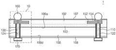
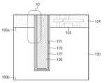
도 1은 본 발명의 실시예에 따른 반도체 소자를 도시한 단면도이다.1 is a cross-sectional view showing a semiconductor device according to an embodiment of the present invention.
도 1을 참조하면, 반도체 소자(1)는 전기적 신호를 기판(100)을 수직 관통하여 전달하는 전기적 연결부(10)를 포함할 수 있다. 전기적 연결부(10)는 기판(100)을 실질적으로 수직 관통하는 관통전극(130)을 포함할 수 있다. 관통전극(130)과 기판(100) 사이에는 관통전극(130)을 기판(100)으로부터 절연시키는 비아절연막(110)이 제공될 수 있다. 관통전극(130)과 비아절연막(110) 사이에 관통전극(130)의 구성 성분(예: 구리)이 기판(100)으로 확산하는 것을 저지할 수 있는 배리어막(122)이 더 제공될 수 있다.Referring to FIG. 1, the
관통전극(130)은 비아절연막(110) 혹은 배리어막(122) 상에 씨드막(124)을 증착하고, 씨드막(124)을 이용한 전기도금으로 형성할 수 있다. 본 실시예에 따르면, 씨드막(124)을 형성하고 인시튜(in-situ)로 어닐링 공정을 진행하여 씨드막(124)의 표면 거칠기(surface roughness)를 개선시키는 것을 포함할 수 있다. 이에 따르면, 관통전극(130)의 박리 현상을 억제할 수 있다. 이에 대해서는 도 2e 내지 2f를 참조하여 상세히 후술한다.The penetrating
반도체 소자(1)는 관통전극(130)과 전기적으로 연결되는 상부단자(160)와 하부단자(170) 중 적어도 어느 하나를 더 포함할 수 있다. 상부단자(160)는 기판(100)의 활성면(100a) 상에 하부단자(170)는 기판(100)의 비활성면(100d) 상에 배치될 수 있다. 상부단자(160)와 하부단자(170)는 솔더볼, 솔더범프, 재배선, 패드 등을 포함할 수 있다. 일례로, 상부단자(160)는 솔더볼을 하부단자(170)는 패드를 포함할 수 있다.The
기판(100)의 활성면(100a) 상에는 집적회로(103), 집적회로(103)와 전기적으로 연결되는 단층 혹은 복층 구조의 금속배선(152), 그리고 집적회로(103)와 금속배선(152)을 덮는 층간절연막(102)이 배치될 수 있다. 층간절연막(102) 상에는 상부단자(160)가 접속되는 본딩패드(154)를 열어놓는 상부절연막(107)이 배치될 수 있다. 금속배선(152)과 관통전극(130)이 전기적으로 연결되므로써 집적회로(103)와 관통전극(130)이 전기적으로 연결될 수 있다. 관통전극(130)은 집적회로(103)의 주위에 혹은 집적회로(103) 내에 배치될 수 있다. 기판(100)의 비활성면(100d) 상에는 하부절연막(108)이 배치될 수 있다. 전기적 연결부(10)는 이하에서 후술한 바와 같이 다양한 구조를 포함할 수 있다.
A single-layer or
<반도체 소자의 제조방법예 1><Method of
도 2a 내지 2l은 본 발명의 일 실시예에 따른 반도체 소자의 제조방법을 도시한 단면도들이다.2A to 2L are cross-sectional views illustrating a method of manufacturing a semiconductor device according to an embodiment of the present invention.
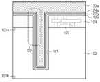
도 2a를 참조하면, 기판(100)에 비아홀(101)을 형성할 수 있다. 기판(100)은 집적회로(103)가 형성된 상면(100a)과 그 반대면인 제1 하면(100b)을 갖는 반도체 기판, 가령 실리콘 기판일 수 있다. 기판(100)의 상면(100a) 상에는 집적회로(103)를 덮는 제1 층간절연막(104)이 형성되어 있을 수 있다. 집적회로(103)는 메모리 회로, 로직 회로 혹은 이들의 조합일 수 있다. 제1 층간절연막(104)은 실리콘산화막이나 실리콘질화막을 증착하여 형성할 수 있다. 비아홀(101)은 기판(100)의 상면(100a)을 향해 개구되고 제1 하면(100b)에 이르지 않는 속이 빈 기둥(hollow pillar) 형태로 형성할 수 있다. 비아홀(101)은 기판(100)의 상면(100a)에서부터 제1 하면(100b)을 향해 실질적으로 수직할 수 있다. 비아홀(101)은 집적회로(103)의 주위, 가령 스크레이브 레인이나 이에 인접한 영역 혹은 집적회로(103)가 형성된 영역에 상당하는 제1 층간절연막(104)과 기판(100)을 건식 식각하여 형성할 수 있다. 일례로서, 비아홀(101)은 종횡비(aspect ratio)가 10:1 이상, 가령 수 ㎛의 폭(W)과 수십 ㎛의 길이(H)를 가질 수 있다.Referring to FIG. 2A, a via
도 2b를 참조하면, 비아홀(101)의 내면을 따라 연장되는 절연막(110a)을 형성하고, 비아홀(101)이 채워지도록 기판(100) 상에 도전막(130a)을 형성할 수 있다. 절연막(110a)은 실리콘산화막이나 실리콘질화막을 증착하여 형성할 수 있다. 도전막(130a)은 폴리실리콘, 구리, 텅스텐, 알루미늄 등을 증착하거나 도금하여 형성할 수 있다. 도전막(130a)을 구리 혹은 구리를 포함하는 도전체로 형성할 경우 구리의 확산을 저지할 수 있는 금속막(122a)을 절연막(110a) 상에 더 형성할 수 있다. 금속막(122a)은 타이타늄(Ti), 타이타늄질화물(TiN), 크롬(Cr), 탄탈륨(Ta), 탄탈륨질화물(TaN), 니켈(Ni), 텅스텐(W), 텅스텐나이트라이드(WN), 혹은 이들의 조합을 포함하는 금속을 증착하여 절연막(110a)을 따라 연장되는 형태로 형성할 수 있다.Referring to FIG. 2B, an insulating
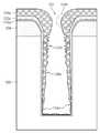
본 실시예에 따르면, 도전막(130a)은 구리를 전기도금하여 형성할 수 있다. 일례로, 절연막(110a) 혹은 금속막(122a) 상에 씨드막(124a)을 형성하고 씨드막(124a)을 이용한 전기도금으로 도전막(130a)을 형성할 수 있다. 씨드막(124a)은 금속을 증착하여 형성할 수 있다. 씨드막(124a)은 두께가 불균일하게 형성될 수 있다. 이에 대해선 도 2b의 일부(50)를 확대 도시한 도 2c를 참조하여 상세히 설명한다.According to the present embodiment, the
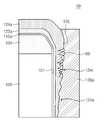
도 2c를 도 2b와 같이 참조하면, 비아홀(101)은 입구가 상대적으로 넓은 깔대기 형상을 가질 수 있다. 예컨대, 건식 식각으로 비아홀(101)을 형성하는 경우 제1 층간절연막(104)의 모서리가 더 식각되므로써 기판(100)을 향해 내려갈수록 내리막 경사진 경사면(101s)이 형성될 수 있다. 다른 예로, 비아홀(101)은 대체로 수직한 기둥 형태를 가질 수 있다.Referring to FIG. 2C, referring to FIG. 2B, the via
씨드막(124a)은 구리(Cu) 혹은 구리망간(CuMn) 등 구리를 포함하는 금속을 물리적기상증착(PVD)하여 형성할 수 있다. 씨드막(124a)은 비아홀(101)의 측면 및 바닥면에서의 스텝 커버리지(step coverage)를 확보하기 위해 비교적 두껍게 형성할 수 있다. 일례로, 비아홀(101)이 도 2a에서 설명한 것처럼 수 ㎛의 폭(W)과 수십 ㎛의 길이(H)를 가지는 경우 씨드막(124a)은 수십 내지 수백 nm의 두께를 가지도록 형성할 수 있다. 물리적기상층착의 특성에 의해 씨드막(124a)은 비아홀(101)의 입구에선 큰 두께를 아래로 내려갈수록 작은 두께를 가지는 불균일한 두께를 가질 수 있다. 아울러, 비아홀(101)의 상단부에선 모폴로지(morphology)가 상대적으로 거친 표면(124r)과 비아홀(101)의 하단부에선 상대적으로 매끄러운 표면(124s)을 갖는 씨드막(124a)이 형성될 수 있다. 다시 말해, 씨드막(124a)은 표면거칠기(surface roughness)가 큰 표면(124r)과 작은 표면(124s)을 가질 수 있다. 이는 물리적기상증착에 있어서 기판(100)을 향해 수직하게 내려오는 입자 이외에 비스듬히 내려오는 입자에 의해 상단부가 두껍고 거친 표면(124r)을 갖는 씨드막(124a)이 형성되는 것이라 여겨진다.The
도 2d에 도시된 바와 같이, 씨드막(124a)을 이용한 전기도금으로 도전막(130a)을 형성하면 거친 표면(124r)이 금속으로 완전히 채워지지 못하므로써 도전막(130a)과 씨드막(124a) 간의 경계(125)에서 보이드(60)가 생성될 수 있다. 보이드(60)에 의해 가령 후속하는 화학기계적연마(CMP) 혹은 어닐링 공정 등에서 관통전극(도 2h의 130)이 박리되는 현상이 일어날 수 있다.2d, when the
도 2e를 참조하면, 일 실시예에 따르면 씨드막(124a)을 형성하고 인시튜(in-situ)로 어닐링하므로써 거친 표면(124r,124s)을 매끄럽게 개선할 수 있다. 즉, 상기 어닐링으로써 씨드막(124a)을 리플로우시켜 표면(124r,124s)의 거칠기(roughness)를 개선할 수 있다. 본 실시예에 따르면, 대체로 표면거칠기가 큰 표면(124r)이 개선될 수 있다. 상기 인시튜 어닐링은 대기압보다 낮은 압력, 가령 (고)진공 상태에서 대략 150 내지 350℃ 혹은 150 내지 250℃ 온도에서 진행할 수 있다. 상기 온도 범위보다 낮은 온도로 어닐링을 진행하게 되면 씨드막(124a)의 리플로우가 어려워질 수 있고, 상기 온도 범위보다 높으면 씨드막(124a)의 응집(aggregation)이 일어날 수 있다. 어닐링은 1 내지 20분 동안 진행될 수 있다. 상기 인시튜 어닐링 공정은 씨드막(124a)을 형성하고 진공 상태를 계속 유지하면서 동일 챔버 혹은 다른 챔버에서 진행될 수 있다.Referring to FIG. 2E, it is possible to smoothly improve the
도 2f를 참조하면, 씨드막(124a)을 인시튜 어닐링한 후 도전막(130a)을 전기도금하면 씨드막(124a)의 거친 표면(124r,124s)이 매끄럽게 개선되므로써 씨드막(124a)과 도전막(130a)의 계면에서 보이드가 생성되지 아니할 수 있다. 다른 예로, 도 2g에 도시된 것처럼, 경사면(101s)은 제1 층간절연막(104)과 층간절연막(104)에 인접한 기판(100)까지 확장될 수 있다.2F, when the
도 2h를 참조하면, 평탄화 공정으로 제1 층간절연막(104)을 노출시킬 수 있다. 평탄화는 에치백이나 화학기계적 연마 공정으로 진행할 수 있다. 상기 평탄화에 의해 도전막(130a)은 기판(100)과 제1 층간절연막(104)을 대체로 수직 관통하는 기둥 형태의 관통전극(130)으로 형성되고, 절연막(110a)은 관통전극(130)을 기판(100)으로부터 전기적으로 절연시키는 비아절연막(110)으로 형성될 수 있다. 금속막(122a)을 더 형성한 경우, 상기 평탄화에 의해 금속막(122a)은 관통전극(130)을 이루는 성분(예: Cu)이 기판(100)이나 집적회로(103)로 확산하는 것을 방지하는 배리어막(122)으로 형성될 수 있다.Referring to FIG. 2H, the first
도 2i를 참조하면, 씨드막(124a)은 관통전극(130)의 일부를 이룰 수 있다. 씨드막(124a)이 관통전극(130)과 동일 또는 유사한 금속을 포함하는 경우 씨드막(124a)과 관통전극(130)의 경계(125)는 보이지 않을 수 있다. 이와 다르게, 씨드막(124a)이 관통전극(130)과 상이한 금속을 포함하는 경우 경계(125)는 보여질 수 있을 것이다. 가령, 경계(125)는 비아홀(101)을 따라 구불구불하게 연장된 형태를 가질 수 있다.Referring to FIG. 2I, the
도 2j를 참조하면, 백 엔드(Back End) 공정을 진행할 수 있다. 일례로, 제1 층간절연막(104) 상에 관통전극(130)과 접속하는 단층 혹은 복층의 금속배선(152)과, 금속배선(152)과 전기적으로 연결되는 본딩패드(154)와, 그리고 금속배선(152)과 본딩패드(154)를 덮는 제2 층간절연막(106)을 형성할 수 있다. 금속배선(152)과 본딩패드(154)는 구리나 알루미늄 등과 같은 금속을 증착하고 패터닝하여 형성할 수 있다. 제2 층간절연막(106)은 제1 층간절연막(104)과 동일하거나 유사한 절연체, 가령 실리콘산화막이나 실리콘질화막을 증착하여 형성할 수 있다. 제2 층간절연막(106) 상에 상부절연막(107)을 형성할 수 있다. 상부절연막(107)은 실리콘산화막, 실리콘질화막 혹은 폴리머 등을 증착한 후 패터닝하여 본딩패드(154)를 노출시키는 형태로 형성할 수 있다. 선택적으로 범프 공정을 더 진행하여 본딩패드(154)와 접속되는 솔더볼이나 솔더범프와 같은 상부단자(160)를 더 형성할 수 있다. 제1 층간절연막(104)과 제2 층간절연막(106)이 기판(100)과 상부절연막(107) 사이의 층간절연막(102)을 구성할 수 있다.Referring to FIG. 2J, a back end process can be performed. For example, on the first
도 2k를 참조하면, 기판(100)을 리세스하여 관통전극(130)을 돌출시킬 수 있다. 가령, 기판(100)을 구성하는 물질(예: 실리콘)을 선택적으로 제거할 수 있는 에천트나 슬러리를 이용한 식각, 화학기계적 연마, 그라인딩, 혹은 이들의 조합으로 기판(100)의 제1 하면(100b)을 리세스할 수 있다. 상기 리세스 공정은 제1 하면(100b)에 비해 상면(100a)에 더 인접하여 관통전극(130)의 하단부(130p)를 돌출시킬 수 있는 제3 하면(100d)이 드러날 때까지 진행할 수 있다. 일례로, 관통전극(130)을 노출시키지 않는 제2 하면(100c)이 드러나도록 기판(100)의 제1 하면(100b)을 화학기계적연마(CMP)하고, 제2 하면(100c)을 건식 식각하여 제3 하면(100d)까지 기판(100)을 더 리세스할 수 있다. 관통전극(130)을 돌출시키는 공정은 기판(100)의 상면(100a) 상에 접착막(72)의 개재하에 캐리어(70)가 부착된 상태에서 진행될 수 있다. 상기 관통전극(130)의 돌출 공정은 기판(100)의 상면(100a)이 위를 향한 상태로 혹은 기판(100)을 뒤집어 상면(100a)이 아래를 향한 상태에서 진행될 수 있다. 본 명세서에서 기판(100)의 상면(100a)은 활성면일 수 있고, 제3 하면(100d)은 비활성면일 수 있다.Referring to FIG. 2K, the
도 2l을 참조하면, 기판(100)의 비활성면(100d) 상에 하부절연막(108)을 형성할 수 있다. 일례로, 비활성면(100d) 상에 관통전극(130)을 덮는 실리콘산화막이나 실리콘질화막을 증착한 후 화학기계적 연마하여 평탄화된 하부절연막(108)을 형성할 수 있다. 관통전극(130)은 하부절연막(108)을 통해 노출될 수 있다. 그리고 하부절연막(108) 상에 관통전극(130)과 전기적으로 연결되는 하부단자(170)를 형성할 수 있다. 하부단자(170)와 관통전극(130) 사이에 금속막(172)을 더 형성하고 하부단자(170)를 덮는 도금막(174)을 더 형성할 수 있다. 상기 일련의 공정을 통해 전기적 연결부(11)를 갖는 도 1의 반도체 소자(1)를 형성할 수 있다.
Referring to FIG. 21, a lower insulating
<반도체 소자의 제조방법예 2>≪ Semiconductor Device Manufacturing Method Example 2 &
도 3a 내지 3e는 본 발명의 다른 실시예에 따른 반도체 소자의 제조방법을 도시한 단면도들이다.3A to 3E are cross-sectional views illustrating a method of manufacturing a semiconductor device according to another embodiment of the present invention.
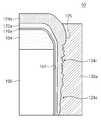
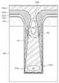
도 3a를 참조하면, 도 2a 및 2b에서 설명한 바와 동일 또는 유사한 공정으로 기판(100)에 비아홀(101)을 형성하고, 비아홀(101)의 내면을 따라 연장되는 절연막(110a)을 형성하고, 절연막(110a) 상에 금속을 물리적기상증착하여 씨드막(124a)을 형성할 수 있다. 절연막(110a)과 씨드막(124a) 사이에 금속막(122a)을 더 형성할 수 있다. 씨드막(124a)은 오버행(124h)을 가지며 불연속적인 프로파일을 가지도록 형성될 수 있다. 이에 대해선 도 3a의 일부를 확대 도시한 도 3b를 참조하여 상세히 설명한다.3A, a via
도 3b를 참조하면, 씨드막(124a)은 물리적기상증착 특성에 의해 비아홀(101)의 상단부에선 오버행(124h)을 가지며, 비아홀(101)의 하단부에선 금속이 불완전하게 증착되거나 혹은 증착되지 않아 생성된 절단부(124d)를 가질 수 있다. 도 2b에서와 마찬가지로, 씨드막(124a)은 비아홀(101)의 입구에선 큰 두께를 아래로 내려갈수록 작은 두께를 가지는 불균일한 두께를 가지며, 비아홀(101)의 상단부에선 모폴로지(morphology)가 상대적으로 거친 표면(124r)과 비아홀(101)의 하단부에선 상대적으로 매끄러운 표면(124s)을 가질 수 있다.3B, the
도 3c에 도시된 바와 같이, 본 실시예와 다르게 씨드막(124a)의 인시튜 어닐링을 하지 아니하고 씨드막(124a)을 이용한 전기도금으로 도전막(130a)을 형성하게 되면 도전막(130a)은 오버행(124h)에 의해 핀치-오프(pinch off)되어 생성되는 보이드(62), 및/또는 절단부(124d)에 의해 금속이 불완전하게 도금되거나 혹은 도금되지 않아 생성되는 보이드(64)를 가질 수 있다. 도 2d에서와 마찬가지로, 표면(124r)이 금속으로 완전히 채워지지 못하므로써 보이드(60)가 생성될 수 있다.As shown in FIG. 3C, when the
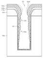
도 3d를 참조하면, 일 실시예에 따르면 씨드막(124a)을 형성하고 인시튜로 어닐링할 수 있다. 상기 인시튜 어닐링에 의해 씨드막(124a)이 리플로우되므로써 오버행(124) 및/또는 절단부(도 3b의 124d)가 제거되거나 완화되어 씨드막(124a)의 프로파일 내지 스텝 커버리지가 개선될 수 있다. 아울러, 상기 리플로우는 씨드막(124a)의 거친 표면(124r,124s)을 매끄럽게 개선시킬 수 있다. 상기 인시튜 어닐링은 도 2e에서 설명한 바와 동일 또는 유사한 공정 조건에서 진행될 수 있다.Referring to FIG. 3D, according to an embodiment, a
도 3e를 참조하면, 씨드막(124a)을 인시튜 어닐링한 후 전기도금으로 도전막(130a)을 형성할 수 있다. 씨드막(124a)의 프로파일 내지 스텝 커버리지가 개선되므로써 보이드 없는 도전막(130a)이 형성될 수 있다. 이어서, 도 2h 내지 2l에서 설명한 바와 동일 또는 유사한 공정으로 도 2l과 같은 전기적 연결부(11)를 갖는 도 1의 반도체 소자(1)를 형성할 수 있다.
Referring to FIG. 3E, after the
<전기적 연결부의 다른 예><Other examples of electrical connections>
도 4a 내지 4c는 도 2l의 변형예들을 도시한 단면도들이다. 이하에선 도 2l과 상이한 점에 대해서 상설하고 동일한 점에 대해서는 생략한다.Figs. 4A to 4C are cross-sectional views showing modifications of Fig. Hereinafter, the points are different from those in Fig. 21, and the same points are omitted.
도 4a를 참조하면, 전기적 연결부(12)는 집적회로(103)와 금속배선(152)이 형성된 이후에 형성된 관통전극(130)을 포함할 수 있다. 관통전극(130)은 층간절연막(102)과 기판(100)을 관통하는 기둥 형태일 수 있다. 상부절연막(107) 상에는 관통전극(130)과 본딩패드(154)를 전기적으로 연결하는 상부배선(153)이 더 배치될 수 있다. 관통전극(130)은 상부절연막(107)을 더 관통하여 상부배선(153)과 접속될 수 있다. 관통전극(130)의 상단 일부(50)는 도 2i와 동일 또는 유사한 구조를 가질 수 있다.Referring to FIG. 4A, the
도 4b를 참조하면, 전기적 연결부(13)는 관통전극(130)이 형성된 이후에 집적회로(103)와 금속배선(152)이 형성되기 이전에 형성된 관통전극(130)을 포함할 수 있다. 기판(100)의 활성면(100a) 상에 기판(100)과는 전기적으로 절연되며 관통전극(130)과는 전기적으로 연결되는 연결배선(156)이 더 제공될 수 있다. 관통전극(130)은 연결배선(156)과 금속배선(152)을 연결하는 연결비아(158)를 통해 금속배선(152) 및/또는 집적회로(103)와 전기적으로 연결되는 기판(100)을 관통하는 기둥 형태일 수 있다. 관통전극(130)의 상단 일부(50)는 도 2i와 동일 또는 유사한 구조를 가질 수 있다.Referring to FIG. 4B, the
도 4c를 참조하면, 전기적 연결부(14)는 집적회로(103)와 금속배선(152)이 형성된 이후에 기판(100)을 리세스한 이후에 형성된 관통전극(130)을 포함할 수 있다. 배리어막(122)은 연결배선(156)에 접하는 부분은 닫히고 하부단자(170)에 접하는 부분은 열린 컵 형태를 가질 수 있다. 관통전극(130)의 하단 일부(50)는 도 2i와 동일 또는 유사한 구조를 가질 수 있다.
Referring to FIG. 4C, the
<반도체 소자의 응용예><Application example of semiconductor device>
도 5a는 본 발명의 실시예에 따른 반도체 소자를 구비한 메모리 카드를 도시한 블록도이다. 도 5b는 본 발명의 실시예에 따른 반도체 소자를 응용한 정보 처리 시스템을 도시한 블록도이다.5A is a block diagram illustrating a memory card having a semiconductor device according to an embodiment of the present invention. 5B is a block diagram illustrating an information processing system using a semiconductor device according to an embodiment of the present invention.
도 5a를 참조하면, 상술한 본 발명의 실시예에 따른 반도체 소자(1)를 적어도 하나 포함하는 메모리(1210)는 메모리 카드(1200)에 응용될 수 있다. 일례로, 메모리 카드(1200)는 호스트(1230)와 메모리(1210) 간의 제반 데이터 교환을 제어하는 메모리 컨트롤러(1220)를 포함할 수 있다. 에스램(1221)은 중앙처리장치(1222)의 동작 메모리로서 사용될 수 있다. 호스트 인터페이스(1223)는 메모리 카드(1200)와 접속되는 호스트(1230)의 데이터 교환 프로토콜을 구비할 수 있다. 오류 수정 코드(1224)는 메모리(1210)로부터 독출된 데이터에 포함되는 오류를 검출 및 정정할 수 있다. 메모리 인터페이스(1225)는 메모리(1210)와 인터페이싱할 수 있다. 중앙처리장치(1222)는 메모리 컨트롤러(1220)의 데이터 교환을 위한 제반 제어 동작을 수행할 수 있다.Referring to FIG. 5A, the
도 5b를 참조하면, 정보 처리 시스템(1300)은 본 발명의 실시예에 따른 반도체 소자(1)를 적어도 하나 구비한 메모리 시스템(1310)을 포함할 수 있다. 정보 처리 시스템(1300)은 모바일 기기나 컴퓨터 등을 포함할 수 있다. 일례로, 정보 처리 시스템(1300)은 메모리 시스템(1310)과 각각 시스템 버스(1360)에 전기적으로 연결된 모뎀(1320), 중앙처리장치(1330), 램(1340), 유저인터페이스(1350)를 포함할 수 있다. 메모리 시스템(1310)은 메모리(1311)와 메모리 컨트롤러(1312)를 포함하며, 도 5a의 메모리 카드(1200)와 실질적으로 동일하게 구성될 수 있다. 이러한 메모리 시스템(1310)에는 중앙처리장치(1330)에 의해서 처리된 데이터 또는 외부에서 입력된 데이터가 저장될 수 있다. 정보 처리 시스템(1300)은 메모리 카드, 반도체 디스크 장치(Solid State Disk), 카메라 이미지 프로세서(Camera Image Sensor) 및 그 밖의 응용 칩셋(Application Chipset)으로 제공될 수 있다. 일례로, 메모리 시스템(1310)은 반도체 디스크 장치(SSD)로 구성될 수 있으며, 이 경우 정보 처리 시스템(1300)은 대용량의 데이터를 메모리 시스템(1310)에 안정적으로 그리고 신뢰성있게 저장할 수 있다.
Referring to FIG. 5B, the
이상의 발명의 상세한 설명은 개시된 실시 상태로 본 발명을 제한하려는 의도가 아니며, 본 발명의 요지를 벗어나지 않는 범위 내에서 다양한 다른 조합, 변경 및 환경에서 사용할 수 있다. 첨부된 청구범위는 다른 실시 상태도 포함하는 것으로 해석되어야 할 것이다.It is not intended to be exhaustive or to limit the invention to the precise form disclosed, and it will be apparent to those skilled in the art that various modifications and variations can be made in the present invention without departing from the spirit of the invention. The appended claims should be construed to include other embodiments.
Claims (10)
Translated fromKorean상기 비아홀의 내면을 따라 연장되고 상기 기판의 상면을 덮는 비아절연막을 형성하고;
상기 비아절연막 상에 상기 비아절연막을 따라 연장되는 씨드막을 형성하고;
상기 씨드막을 형성한 후 인시튜로 상기 씨드막을 어닐링하고;
상기 씨드막을 이용한 전기도금으로 상기 비아홀을 채우는 도전막을 형성하고; 그리고
상기 기판의 상면을 평탄화하여 상기 비아홀 내에 상기 비아절연막으로 둘러싸이는 관통전극을 형성하는 것을;
포함하는 반도체 소자의 제조방법.Forming a via hole that opens toward the upper surface of the substrate and does not reach the bottom surface of the substrate;
Forming a via insulating film extending along an inner surface of the via hole and covering an upper surface of the substrate;
Forming a seed film extending along the via insulating film on the via insulating film;
Annealing the seed layer in situ after forming the seed layer;
Forming a conductive film filling the via hole by electroplating using the seed film; And
Planarizing an upper surface of the substrate to form a penetrating electrode surrounded by the via insulating film in the via hole;
Wherein the semiconductor device is a semiconductor device.
상기 씨드막을 형성하는 것은 상기 비아절연막 상에 불균일한 두께를 갖는 금속을 물리적기상증착하는 것을 포함하고,
상기 씨드막은 상기 기판의 상면에 인접한 상기 비아홀의 입구부에서는 큰 두께를 상기 기판의 하면에 인접한 상기 비아홀의 하단에서는 작은 두께를 갖는 반도체 소자의 제조방법.The method according to claim 1,
Forming the seed film comprises physically vapor-depositing a metal having a non-uniform thickness on the via insulating film,
Wherein the seed layer has a large thickness at an inlet portion of the via hole adjacent to an upper surface of the substrate and a small thickness at a lower end of the via hole adjacent to a bottom surface of the substrate.
상기 큰 두께의 씨드막은 상기 작은 두께의 씨드막에 비해 표면 거칠기(surface roughness)가 큰 반도체 소자의 제조방법.3. The method of claim 2,
Wherein the seed film having a large thickness has a larger surface roughness than the seed film having the small thickness.
상기 기판의 하면을 리세스하여 상기 관통전극을 돌출시키고;
상기 리세스된 기판의 하면 상에 상기 관통전극을 덮는 하부절연막을 형성하고; 그리고
상기 하부절연막을 평탄화하여 상기 관통전극을 노출시키는 것을;
더 포함하는 반도체 소자의 제조방법.The method according to claim 1,
The bottom surface of the substrate is recessed to protrude the penetrating electrode;
Forming a lower insulating film on the lower surface of the recessed substrate to cover the penetrating electrode; And
Planarizing the lower insulating film to expose the penetrating electrode;
≪ / RTI >
상기 기판을 일부 관통하며 상기 기판의 상면을 향해 개구된 비아홀을 형성하고;
상기 비아홀의 내면을 덮는 비아절연막을 형성하고;
상기 비아절연막을 덮는 금속막을 물리적기상증착한 후 인시튜로 어닐링하고; 그리고
상기 금속막을 이용한 전기도금으로 상기 비아홀을 채우는 관통전극을 형성하는 것을;
포함하는 반도체 소자의 제조방법.Providing a substrate having an upper surface and a lower surface opposite thereto;
Forming a via hole partially penetrating the substrate and opening toward an upper surface of the substrate;
Forming a via insulating film covering the inner surface of the via hole;
Physical vapor deposition of a metal film covering the via insulating film, and then in-vitro annealing; And
Forming a through electrode for filling the via hole by electroplating using the metal film;
Wherein the semiconductor device is a semiconductor device.
상기 금속막은 상기 기판의 상면에 인접한 상기 비아홀의 입구부에선 거친 제1 표면을 가지며 상기 기판의 하면에 인접한 상기 비아홀의 하단에선 상기 제1 표면에 비해 매끄러운 제2 표면을 갖는 반도체 소자의 제조방법.6. The method of claim 5,
Wherein the metal film has a rough first surface at an inlet portion of the via hole adjacent to an upper surface of the substrate and a second surface at a lower end of the via hole adjacent to the lower surface of the substrate, the second surface being smoother than the first surface.
상기 제1 표면을 갖는 금속막의 두께는 상기 제2 표면을 갖는 금속막의 두께보다 큰 반도체 소자의 제조방법.The method according to claim 6,
Wherein the thickness of the metal film having the first surface is greater than the thickness of the metal film having the second surface.
상기 금속막은 구리를 포함하고,
상기 인시튜 어닐링은 150 내지 350℃ 온도에서 진행하는 것을 포함하는 반도체 소자의 제조방법.6. The method of claim 5,
Wherein the metal film comprises copper,
Wherein the in-situ annealing is performed at a temperature of 150 to 350 占 폚.
상기 인시튜 어닐링은 대기압보다 낮은 압력에서 진행하는 반도체 소자의 제조방법.9. The method of claim 8,
Wherein the in-situ annealing proceeds at a pressure lower than atmospheric pressure.
상기 비아홀을 형성하는 것은 상기 기판을 건식 식각하여 상기 기판의 일부를 관통하는 홀을 형성하는 것을 포함하고,
상기 비아홀의 입구는 상기 기판의 하면으로 갈수록 내리막 경사진 경사면을 갖는 반도체 소자의 제조방법.6. The method of claim 5,
Forming the via hole includes dry-etching the substrate to form a hole penetrating a part of the substrate,
And the entrance of the via hole has an inclined surface inclined downward toward the bottom surface of the substrate.
Priority Applications (2)
| Application Number | Priority Date | Filing Date | Title |
|---|---|---|---|
| KR1020130018704AKR20140104778A (en) | 2013-02-21 | 2013-02-21 | Methods for fabricating semiconductor devices having through vias |
| US14/183,817US9543200B2 (en) | 2013-02-21 | 2014-02-19 | Methods for fabricating semiconductor devices having through electrodes |
Applications Claiming Priority (1)
| Application Number | Priority Date | Filing Date | Title |
|---|---|---|---|
| KR1020130018704AKR20140104778A (en) | 2013-02-21 | 2013-02-21 | Methods for fabricating semiconductor devices having through vias |
Publications (1)
| Publication Number | Publication Date |
|---|---|
| KR20140104778Atrue KR20140104778A (en) | 2014-08-29 |
Family
ID=51351500
Family Applications (1)
| Application Number | Title | Priority Date | Filing Date |
|---|---|---|---|
| KR1020130018704AWithdrawnKR20140104778A (en) | 2013-02-21 | 2013-02-21 | Methods for fabricating semiconductor devices having through vias |
Country Status (2)
| Country | Link |
|---|---|
| US (1) | US9543200B2 (en) |
| KR (1) | KR20140104778A (en) |
Cited By (1)
| Publication number | Priority date | Publication date | Assignee | Title |
|---|---|---|---|---|
| KR20160110658A (en)* | 2015-03-10 | 2016-09-22 | 삼성전자주식회사 | Methods for fabricating semiconductor devices having through electrodes and methods for fabricating the same |
Families Citing this family (10)
| Publication number | Priority date | Publication date | Assignee | Title |
|---|---|---|---|---|
| US9449898B2 (en) | 2013-07-31 | 2016-09-20 | Taiwan Semiconductor Manufacturing Company, Ltd. | Semiconductor device having backside interconnect structure through substrate via and method of forming the same |
| US9837411B2 (en)* | 2015-07-14 | 2017-12-05 | Tower Semiconductors Ltd. | Semiconductor die with a metal via |
| US9899260B2 (en)* | 2016-01-21 | 2018-02-20 | Micron Technology, Inc. | Method for fabricating a semiconductor device |
| JP2019160893A (en)* | 2018-03-09 | 2019-09-19 | ソニーセミコンダクタソリューションズ株式会社 | Solid state imaging element, semiconductor device, electronic device, and manufacturing method |
| US10446729B1 (en)* | 2018-03-22 | 2019-10-15 | Innolux Corporation | Display device having an electronic device disposed on a first pad and a second pad |
| CN109712980B (en)* | 2018-11-21 | 2023-08-08 | 长江存储科技有限责任公司 | Manufacturing method of 3D memory device and 3D memory device |
| US11362066B2 (en)* | 2020-03-26 | 2022-06-14 | Taiwan Semiconductor Manufacturing Company, Ltd. | Semiconductor structure and manufacturing method thereof |
| KR102824470B1 (en)* | 2021-02-23 | 2025-06-26 | 삼성전자주식회사 | Semiconductor device and stacked semiconductor chips |
| CN113097420B (en)* | 2021-04-07 | 2024-04-05 | 京东方科技集团股份有限公司 | Electrode structure, preparation method thereof, display substrate and display device |
| KR102856349B1 (en) | 2021-04-16 | 2025-09-04 | 삼성전자주식회사 | Semiconductor chip and semiconductor package including the same |
Family Cites Families (21)
| Publication number | Priority date | Publication date | Assignee | Title |
|---|---|---|---|---|
| JP2623812B2 (en)* | 1989-01-25 | 1997-06-25 | 日本電気株式会社 | Method for manufacturing semiconductor device |
| US6475903B1 (en) | 1993-12-28 | 2002-11-05 | Intel Corporation | Copper reflow process |
| JP2003318178A (en) | 2002-04-24 | 2003-11-07 | Seiko Epson Corp | Semiconductor device and its manufacturing method, circuit board, and electronic equipment |
| TWI239629B (en)* | 2003-03-17 | 2005-09-11 | Seiko Epson Corp | Method of manufacturing semiconductor device, semiconductor device, circuit substrate and electronic apparatus |
| JP4182340B2 (en) | 2003-03-27 | 2008-11-19 | セイコーエプソン株式会社 | Semiconductor device and manufacturing method thereof, circuit board, and electronic apparatus |
| JP2005026313A (en)* | 2003-06-30 | 2005-01-27 | Shinko Electric Ind Co Ltd | Method of manufacturing wiring board |
| JP4307284B2 (en) | 2004-02-17 | 2009-08-05 | 三洋電機株式会社 | Manufacturing method of semiconductor device |
| US7709958B2 (en)* | 2004-06-18 | 2010-05-04 | Uri Cohen | Methods and structures for interconnect passivation |
| JP2006012889A (en) | 2004-06-22 | 2006-01-12 | Canon Inc | Semiconductor chip manufacturing method and semiconductor device manufacturing method |
| JP4456027B2 (en) | 2005-03-25 | 2010-04-28 | Okiセミコンダクタ株式会社 | Method for manufacturing through conductor |
| US7312148B2 (en)* | 2005-08-08 | 2007-12-25 | Applied Materials, Inc. | Copper barrier reflow process employing high speed optical annealing |
| JP4694305B2 (en) | 2005-08-16 | 2011-06-08 | ルネサスエレクトロニクス株式会社 | Manufacturing method of semiconductor wafer |
| US7629249B2 (en)* | 2006-08-28 | 2009-12-08 | Micron Technology, Inc. | Microfeature workpieces having conductive interconnect structures formed by chemically reactive processes, and associated systems and methods |
| JP2008085238A (en) | 2006-09-29 | 2008-04-10 | Citizen Miyota Co Ltd | Substrate having through electrode, and manufacturing method thereof |
| JP5022683B2 (en) | 2006-11-30 | 2012-09-12 | 株式会社東芝 | Manufacturing method of semiconductor device |
| KR100852602B1 (en) | 2006-12-27 | 2008-08-14 | 동부일렉트로닉스 주식회사 | Method of verifying interconnection reliability and method of manufacturing semiconductor device |
| US7704879B2 (en) | 2007-09-27 | 2010-04-27 | Tokyo Electron Limited | Method of forming low-resistivity recessed features in copper metallization |
| US8247030B2 (en)* | 2008-03-07 | 2012-08-21 | Tokyo Electron Limited | Void-free copper filling of recessed features using a smooth non-agglomerated copper seed layer |
| US7968460B2 (en)* | 2008-06-19 | 2011-06-28 | Micron Technology, Inc. | Semiconductor with through-substrate interconnect |
| US8049327B2 (en) | 2009-01-05 | 2011-11-01 | Taiwan Semiconductor Manufacturing Company, Ltd. | Through-silicon via with scalloped sidewalls |
| KR20110075390A (en) | 2009-12-28 | 2011-07-06 | 주식회사 동부하이텍 | Manufacturing Method of Semiconductor Device |
- 2013
- 2013-02-21KRKR1020130018704Apatent/KR20140104778A/ennot_activeWithdrawn
- 2014
- 2014-02-19USUS14/183,817patent/US9543200B2/enactiveActive
Cited By (1)
| Publication number | Priority date | Publication date | Assignee | Title |
|---|---|---|---|---|
| KR20160110658A (en)* | 2015-03-10 | 2016-09-22 | 삼성전자주식회사 | Methods for fabricating semiconductor devices having through electrodes and methods for fabricating the same |
Also Published As
| Publication number | Publication date |
|---|---|
| US9543200B2 (en) | 2017-01-10 |
| US20140235052A1 (en) | 2014-08-21 |
Similar Documents
| Publication | Publication Date | Title |
|---|---|---|
| KR20140104778A (en) | Methods for fabricating semiconductor devices having through vias | |
| US11469202B2 (en) | Semiconductor device | |
| US20200279802A1 (en) | Plurality of Different Size Metal Layers for a Pad Structure | |
| US11688693B2 (en) | Semiconductor packages and method of manufacture | |
| JP6297126B2 (en) | Package and method of forming transmission line thereof | |
| KR101992352B1 (en) | Semicondctor devices | |
| US9570418B2 (en) | Structure and method for package warpage control using dummy interconnects | |
| US7786581B2 (en) | Method of manufacturing a semiconductor device having an even coating thickness using electro-less plating, and related device | |
| KR101319701B1 (en) | Wafer Backside Interconnect Structure Connected To TSVs | |
| US8592310B2 (en) | Methods of manufacturing a semiconductor device | |
| US9087885B2 (en) | Method of fabricating semiconductor devices having through-silicon via (TSV) structures | |
| TWI387052B (en) | Method for forming a conductive viathrough a semiconductor device structure,method for fabricating a semiconductor device structure,semiconductor device structure,and electronic device | |
| US8791011B2 (en) | Through-silicon via structure formation process | |
| US9490205B2 (en) | Integrated circuit interconnects and methods of making same | |
| KR102411064B1 (en) | Methods for fabricating semiconductor devices having through electrodes and methods for fabricating the same | |
| CN113643994A (en) | Collars and associated systems and methods for metal-under-bump structures | |
| KR20170104045A (en) | Semiconductor devices having through electrodes and methods for fabricating the same | |
| US20220165633A1 (en) | Semiconductor structure having an anti-arcing pattern disposed on a passivation layer and method of fabricating the semiconductor structure | |
| TWI483372B (en) | Through-silicon via and fabrication method thereof | |
| US20250167123A1 (en) | Semiconductor die having a metal plate layer | |
| KR20150019089A (en) | Semiconductor devices having through vias and methods for fabricating the same | |
| US8531041B2 (en) | Semiconductor component having a plated through-hole and method for the production thereof |
Legal Events
| Date | Code | Title | Description |
|---|---|---|---|
| PA0109 | Patent application | Patent event code:PA01091R01D Comment text:Patent Application Patent event date:20130221 | |
| PG1501 | Laying open of application | ||
| PC1203 | Withdrawal of no request for examination | ||
| WITN | Application deemed withdrawn, e.g. because no request for examination was filed or no examination fee was paid |