KR20140103026A - Pattern inspection apparatus and pattern inspection method - Google Patents
Pattern inspection apparatus and pattern inspection methodDownload PDFInfo
- Publication number
- KR20140103026A KR20140103026AKR1020130161427AKR20130161427AKR20140103026AKR 20140103026 AKR20140103026 AKR 20140103026AKR 1020130161427 AKR1020130161427 AKR 1020130161427AKR 20130161427 AKR20130161427 AKR 20130161427AKR 20140103026 AKR20140103026 AKR 20140103026A
- Authority
- KR
- South Korea
- Prior art keywords
- light
- pattern
- image
- light source
- transparent substrate
- Prior art date
- Legal status (The legal status is an assumption and is not a legal conclusion. Google has not performed a legal analysis and makes no representation as to the accuracy of the status listed.)
- Granted
Links
Images


Classifications
- G—PHYSICS
- G01—MEASURING; TESTING
- G01N—INVESTIGATING OR ANALYSING MATERIALS BY DETERMINING THEIR CHEMICAL OR PHYSICAL PROPERTIES
- G01N21/00—Investigating or analysing materials by the use of optical means, i.e. using sub-millimetre waves, infrared, visible or ultraviolet light
- G01N21/84—Systems specially adapted for particular applications
- G01N21/88—Investigating the presence of flaws or contamination
- G01N21/95—Investigating the presence of flaws or contamination characterised by the material or shape of the object to be examined
- G01N21/956—Inspecting patterns on the surface of objects
Landscapes
- Physics & Mathematics (AREA)
- Health & Medical Sciences (AREA)
- Life Sciences & Earth Sciences (AREA)
- Chemical & Material Sciences (AREA)
- Analytical Chemistry (AREA)
- Biochemistry (AREA)
- General Health & Medical Sciences (AREA)
- General Physics & Mathematics (AREA)
- Immunology (AREA)
- Pathology (AREA)
- Investigating Materials By The Use Of Optical Means Adapted For Particular Applications (AREA)
- Length Measuring Devices By Optical Means (AREA)
Abstract
Translated fromKoreanDescription
Translated fromKorean본 발명은, 투명 기재상의 패턴을 검사하는 패턴 검사 장치 및 패턴 검사 방법에 관한 것이다.The present invention relates to a pattern inspection apparatus and a pattern inspection method for inspecting a pattern on a transparent substrate.
스마트폰 등에 이용되는 터치 패널의 제조에서는, PET(폴리에틸렌 텔레프탈레이트) 필름 등의 투명 필름상에 금속 배선 패턴이 형성된다. 인출선인 금속 배선 패턴은 터치 패널의 외측 가장자리부에 형성되고, 터치 패널의 화면인 중앙부에 형성되는 투명 전극 패턴에 접속된다. 근년에는, 터치 패널의 화면을 크게 하기 위해, 외측 가장자리부에 있어서의 금속 배선 패턴의 패턴 요소를 가늘게 하는 것이 행해진다. 이 경우, 종래와 같은 조건에서 같은 크기의 전류를 금속 배선 패턴에 흐르게 하기 때문에, 금속 배선 패턴의 두께를 종래의 것보다 크게 하여(애스펙트비를 높게 하여), 패턴 요소의 단면적이 유지된다.In the manufacture of a touch panel used in a smart phone or the like, a metal wiring pattern is formed on a transparent film such as a PET (polyethylene terephthalate) film. The metal wiring pattern as the lead line is formed on the outer edge portion of the touch panel and connected to the transparent electrode pattern formed at the central portion of the screen of the touch panel. In recent years, in order to enlarge the screen of the touch panel, a pattern element of the metal wiring pattern at the outer edge portion is made thin. In this case, since the current of the same size flows in the metal wiring pattern under the conventional conditions, the cross-sectional area of the pattern element is maintained by making the thickness of the metal wiring pattern larger than that of the conventional one (by increasing the aspect ratio).
또한, 일본국 특허 공개 소62-119444호 공보(문헌 1), 일본국 특허 공개2006-72147호 공보(문헌 2) 및 일본국 특허 공개 2006-105816호 공보(문헌 3)에서는, 투명한 기재의 한쪽의 주면에 조사되는 광의 반사광에 의거하는 반사 화상과, 기재의 다른쪽의 주면에 조사되는 광의 투과광에 의거하는 투과 화상을 취득함으로써, 기재상의 패턴을 검사하는 수법이 개시되어 있다.Further, in Japanese Patent Application Laid-Open No. 62-119444 (Document 1), Japanese Patent Application Laid-Open No. 2006-72147 (Document 2), and Japanese Patent Application Laid-Open No. 2006-105816 (Document 3) Discloses a method of inspecting a pattern on a substrate by obtaining a reflected image based on the reflected light of light to be irradiated on the main surface of the substrate and a transmitted image based on the transmitted light of the light irradiated on the other main surface of the substrate.
그런데, 금속 배선 패턴은, 예를 들어, 금속 박막을 부분적으로 에칭함으로써 형성된다. 이때, 에칭 조건에 의해서는 패턴 요소의 상면이 거칠어진 상태가 되거나, 패턴 요소가 샤프하게 에칭되지 않은 것이 있다. 따라서, 패턴 요소의 상면과, 패턴 요소의 끝부분(하부)의 쌍방을 검사하는 요구가 높아지고 있다. 전자 인쇄 기술에 의해 금속 배선 패턴을 형성하는 경우에는, 패턴 요소의 끝부분이 퍼지기 쉽기 때문에, 금속 배선 패턴에 있어서의 끝부분의 검사의 필요성이 더 높아진다.Incidentally, the metal wiring pattern is formed, for example, by partially etching the metal thin film. At this time, depending on the etching conditions, the upper surface of the pattern element becomes rough or the pattern element is not sharply etched. Accordingly, there is a growing demand for inspecting both the upper surface of the pattern element and the end portion (lower portion) of the pattern element. In the case of forming the metal wiring pattern by the electronic printing technique, since the end portion of the pattern element is easy to spread, the necessity of inspection of the end portion in the metal wiring pattern becomes higher.
이 경우에, 상기와 같이 미세한 패턴 요소의 화상을 취득하려면, 고해상도의(NA(개구수)가 높은) 광학계가 필요하다. 한편, 고해상도의 광학계에서는, 초점심도가 얕아져, 패턴 요소의 상면과 끝부분의 사이의 거리보다 작아진다. 따라서, 패턴 요소의 상면과 끝부분을 검사하려면, 포커스 위치를 변경한 2회의 화상 취득이 필요하다. 또, 문헌 1 내지 3의 수법을 응용하여, 패턴 요소의 상면을 나타내는 반사 화상과, 패턴 요소의 끝부분을 나타내는 투과 화상을 취득하는 것도 생각할 수 있다. 그러나, 어느 경우여도, 오버 에칭 등에 의해 패턴 요소의 끝부분이 가늘어져 있을 때에는, 패턴 요소의 끝부분 상태를 취득할 수 없다. 따라서, 패턴 요소의 끝부분에 있어서의 두꺼워짐이나 가늘어짐를 용이하게 검사하는 것이 가능한 신규 수법이 요구된다.In this case, in order to acquire images of the fine pattern elements as described above, a high-resolution optical system (having a high numerical aperture (NA)) is required. On the other hand, in a high-resolution optical system, the depth of focus becomes shallow and becomes smaller than the distance between the top surface and the end portion of the pattern element. Therefore, in order to inspect the top and end portions of the pattern element, it is necessary to obtain two images with the focus position changed. It is also conceivable to obtain a reflection image representing the upper surface of the pattern element and a transmission image representing the end portion of the pattern element by applying the techniques of the
본 발명은, 투명 기재상의 패턴을 검사하는 패턴 검사 장치를 위한 것이며, 패턴 요소의 끝부분에 있어서의 두꺼워짐이나 가늘어짐을 용이하게 검사하는 것을 목적으로 하고 있다.The present invention is directed to a pattern inspection apparatus for inspecting a pattern on a transparent substrate, and aims at easily inspecting thickening and tapering at the end of the pattern element.
본 발명에 따른 패턴 검사 장치는, 판형상 또는 필름형상의 투명 기재에 있어서 패턴이 형성된 한쪽의 주면에 제1 광원부로부터의 광을 조사하고, 상기 패턴의 상면으로부터의 상기 광의 반사광을 제1 수광부에서 수광하여 상면 반사 화상을 취득하는 제1 화상 취득부와, 상기 투명 기재의 다른쪽의 주면에 제2 광원부로부터의 광을 조사하고, 상기 한쪽의 주면에 접하는 상기 패턴의 하면으로부터의 상기 광의 반사광을 제2 수광부에서 수광하여 하면 반사 화상을 취득하는 제2 화상 취득부와, 상기 상면 반사 화상과 상기 하면 반사 화상에 의거하여 상기 패턴의 검사 결과를 취득하는 검사부를 구비한다. 본 발명에 의하면, 패턴 요소의 끝부분에 있어서의 두꺼워짐이나 가늘어짐를 용이하게 검사할 수 있다.The pattern inspection apparatus according to the present invention irradiates light from the first light source part to one main surface of a plate-like or film-like transparent substrate on which a pattern is formed, and transmits the light reflected from the upper surface of the pattern to the first light- A first image acquisition unit for acquiring a top-reflected image by receiving light; and a second image acquisition unit for irradiating light to the other main surface of the transparent substrate from the second light source unit, A second image capturing section for capturing a reflected image when light is received by the second light receiving section and an inspection section for obtaining the inspection result of the pattern on the basis of the top reflection image and the bottom reflection image. According to the present invention, thickening or tapering at the end portion of the pattern element can be easily checked.
본 발명의 한가지 바람직한 형태에서는, 상기 제1 광원부가, 제1 파장대의 광을 출사하고, 상기 제2 광원부가, 상기 제1 파장대와 상이한 제2 파장대의 광을 출사하며, 상기 제1 화상 취득부가, 상기 제2 파장대의 광이 상기 제1 수광부에 입사하는 것을 방지하는 광학 소자를 가지고, 상기 제2 화상 취득부가, 상기 제1 파장대의 광이 상기 제2 수광부에 입사하는 것을 방지하는 광학 소자를 가지며, 상기 상면 반사 화상과 상기 하면 반사 화상이 동시에 취득된다. 이에 의해, 투명 기재상의 패턴의 검사를 고속으로 행하는 것이 실현된다.In one preferred form of the present invention, the first light source unit emits light of a first wavelength band, and the second light source unit emits light of a second wavelength band different from the first wavelength band, And an optical element for preventing the light of the second wavelength range from entering the first light receiving portion, wherein the second image capturing portion includes an optical element for preventing the light of the first wavelength range from entering the second light receiving portion And the upper surface reflection image and the lower surface reflection image are acquired at the same time. Thus, it is possible to inspect the pattern on the transparent substrate at a high speed.
본 발명의 다른 바람직한 형태에서는, 패턴 검사 장치가, 상기 제1 광원부 또는 상기 제2 광원부로부터 출사되고, 상기 투명 기재를 투과한 광을 수광하여 투과 화상을 취득하는 제3 화상 취득부를 더 구비한다. 이에 의해, 패턴 요소의 상면에 있어서의 오목부를 검출하는 것이 용이해진다.In another preferred embodiment of the present invention, the pattern inspection apparatus further comprises a third image acquisition section that receives the light emitted from the first light source section or the second light source section and transmitted through the transparent substrate to acquire a transmission image. This makes it easy to detect the concave portion on the upper surface of the pattern element.
상기 패턴은 금속에서 형성되는 것이 바람직하다.The pattern is preferably formed of a metal.
본 발명은, 패턴 검사 장치를 이용하여 투명 기재상의 패턴을 검사하는 패턴 검사 방법을 위한 것이다.The present invention relates to a pattern inspection method for inspecting a pattern on a transparent substrate using a pattern inspection apparatus.
상기 서술의 목적 및 다른 목적, 특징, 양태 및 이점은, 첨부한 도면을 참조하여 이하에 행하는 이 발명의 상세한 설명에 의해 분명해진다.The above and other objects, features, aspects and advantages of the present invention will become apparent from the following detailed description of the present invention when taken in conjunction with the accompanying drawings.
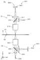
도 1은, 패턴 검사 장치의 구성을 도시하는 도이다.
도 2는, 화상 취득 유닛의 내부 구성을 도시하는 도이다.
도 3은, 투명 기재상의 패턴을 검사하는 동작의 흐름을 도시하는 도이다.
도 4는, 투명 기재상의 패턴을 도시하는 단면도이다.
도 5는, 투명 기재상의 패턴을 도시하는 단면도이다.
도 6은, 상면 반사 화상 및 하면 반사 화상에 있어서의 휘도값의 변화를 도시하는 도이다.
도 7은, 상면 반사 화상 및 하면 반사 화상에 있어서의 휘도값의 변화를 도시하는 도이다.
도 8은, 패턴 요소를 도시하는 평면도이다.
도 9는, 투과 화상을 도시하는 도이다.
도 10은, 상면 반사 화상을 도시하는 도이다.
도 11은, 다른 실시 형태에 따른 패턴 검사 장치에 있어서의 화상 취득 유닛의 구성을 도시하는 도이다.1 is a diagram showing a configuration of a pattern inspection apparatus.
2 is a diagram showing the internal configuration of the image acquisition unit.
3 is a diagram showing a flow of an operation for inspecting a pattern on a transparent substrate.
4 is a cross-sectional view showing a pattern on a transparent substrate.
5 is a cross-sectional view showing a pattern on a transparent substrate.
Fig. 6 is a graph showing the change in the luminance value in the top-side reflection image and the bottom-side reflection image.
Fig. 7 is a graph showing the change in the luminance value in the top-side reflection image and the bottom-reflection image.
8 is a plan view showing a pattern element.
9 is a diagram showing a transmission image.
10 is a diagram showing a top surface reflection image.
11 is a diagram showing a configuration of an image acquisition unit in a pattern inspection apparatus according to another embodiment.
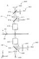
도 1은, 본 발명의 한가지 실시 형태에 따른 패턴 검사 장치(1)의 구성을 도시하는 도이다. 패턴 검사 장치(1)는, 수지제의 투명 기재(9)(예를 들어, PET필름)상에 금속으로 형성된 패턴을 검사하는 장치이다. 패턴 검사 장치(1)는, 연속 필름인 투명 기재(9)가 연속하는 부위를 도 1 중의 Y방향(이하, 「이동 방향」이라고 한다)에 연속적으로 이동하는 이동 기구(2), 이동 도상의 투명 기재(9)의 화상을 취득하는 화상 취득 유닛(3), 및, 패턴 검사 장치(1)의 전체 제어를 담당하는 제어부(11)를 구비한다. 제어부(11)는, 취득된 화상에 의거하여 패턴의 검사를 행하는 검사부(12)를 가진다. 또한, 검사부(12)는, 제어부(11)로부터 분리하여 설치되어도 된다.1 is a diagram showing the configuration of a
이동 기구(2)는, 도 1 중의 X방향(이동 방향에 수직인 방향)에 긴 2개의 롤러(21)를 가지고, 2개의 롤러(21)는, 화상 취득 유닛(3)을 사이에 두고 이동 방향으로 늘어서 있다. 2개의 롤러(21)의 (-Y)측에는, 검사 전의 투명 기재(9)의 롤을 유지함과 더불어 상기 롤로부터 투명 기재(9)의 각 부위를 송출하는 공급부(22)가 설치된다. 2개의 롤러(21)의 (+Y)측에는, 투명 기재(9)의 검사가 행해진 부위를 롤형상으로 권취하여 유지하는 권취부(23)가 설치된다. 이하의 설명에서는, 단순히 투명 기재(9)라고 하는 경우는 이동 방향으로의 이동 도상의 투명 기재(9)의 부위(즉, 2개의 롤러(21) 사이의 투명 기재(9)의 부위)를 의미하는 것으로 한다. 도 1에 도시하는 바와 같이, 2개의 롤러(21) 사이에 배치된 화상 취득 유닛(3)에서는, 투명 기재(9)는 도 1 중의 Z방향에 수직으로(즉, X방향 및 Y방향으로) 퍼진다.The
도 2는, 화상 취득 유닛(3)의 내부 구성을 도시하는 도이다. 화상 취득 유닛(3)은, 투명 기재(9)의 (+Z)측에 배치되는 제1 광원부(331), 제1 광학계(31), 제1 수광부(341) 및 제3 수광부(343), 및, 투명 기재(9)의 (-Z)측에 배치되는 제2 광원부(332), 제2 광학계(32) 및 제2 수광부(342)를 구비한다. 상세하게는, 제1 광원부(331)는 복수의 발광 다이오드(LED)가 일렬로 배열된 LED 어레이이며, 각 LED는 청색의 파장대의 광을 출사한다. 제1 광원부(331)로부터의 광은, 제1 광학계(31)의 콜리메이터 렌즈(311)에서 콜리메이트되고, 하프 미러(312)에서 반사하여 대물 렌즈(313)에 입사한다. 대물 렌즈(313)를 통과한 광은, 투명 기재(9)의 한쪽의((+Z)측의) 주면인 제1 주면(91)상에 조사된다. 제1 광원부(331)로부터의 광이 조사되는 투명 기재(9)상의 영역은, 이동 방향에 교차하는(바람직하게는, 이동 방향에 직교하는) 선형상 영역이다. 투명 기재(9)의 제1 주면(91)상에는 구리 등의 금속으로 패턴이 형성되어 있고, 대물 렌즈(313)로부터의 광 중 패턴에 조사되는 광은, 상기 패턴에서 반사하고, 다른 영역에 조사되는 광은 투명 기재(9)를 투과한다(후술의 도 4 및 도 5 참조).Fig. 2 is a diagram showing an internal configuration of the
패턴의 상면에서 반사한 광(주로, 패턴의 (+Z)방향을 향하는 면에서 반사한 광)은, 대물 렌즈(313)에 입사하고, 대물 렌즈(313)를 통과한 광이 하프 미러(312) 및 결상 렌즈(314)를 개재하여 다이크로익 미러(315)로 인도된다. 다이크로익 미러(315)는 청색의 파장대의 광을 반사하는 미러이며, 투명 기재(9)로부터의 청색의 광은, 다이크로익 미러(315)에서 반사하여 제1 수광부(341)로 인도된다. 제1 수광부(341)는, 복수의 수광 소자가 일렬로 배열된 라인 센서이고, 투명 기재(9)상의 선형상의 영역으로부터의 청색의 광이, 복수의 수광 소자의 수광면, 즉, 선형상의 수광 영역에서 받아들여진다. 정확히는, 제1 수광부(341)는, 패턴의 상면(즉 패턴의 (+Z)방향을 향하는 면)과 광학적으로 공역인 위치에 배치되어 있고, 이에 의해, 패턴의 상면으로부터의 반사광에 의거하는 라인 화상(화소가 1열로 늘어선 화상)이 제1 수광부(341)에서 취득된다. 라인 화상은 제어부(11)에 순차 출력된다.The light reflected from the upper surface of the pattern (mainly the light reflected from the surface facing the pattern in the + Z direction) is incident on the
제2 광원부(332)도, 제1 광원부(331)와 같은 LED어레이이며, 각 LED는 적색의 파장대의 광을 출사한다. 제2 광원부(332)로부터의 광은, 제2 광학계(32)의 콜리메이터 렌즈(321)에서 콜리메이터되고, 하프 미러(322)를 개재하여 대물 렌즈(323)에 입사한다. 대물 렌즈(323)를 통과한 광은, 투명 기재의(9)의 다른쪽의((-Z)측의) 주면인 제2 주면(92)상에 조사된다. 제2 광원부(332)로부터의 광이 조사되는 투명 기재(9)상의 영역은, 이동 방향에 교차하는(바람직하게는, 이동 방향에 직교하는) 선형상 영역이며, 제1 광원부(331)로부터의 광이 조사되는 선형상 영역과 Z방향에 있어서 거의 겹친다. 대물 렌즈(323)로부터의 광 중, 제1 주면(91)에 접하는(부착하는) 패턴의 하면에 조사되는 광은, 상기 하면에서 반사하고, 다른 영역에 조사되는 광은 투명 기재(9)를 투과한다(후술의 도 4 및 도 5).The second
패턴의 하면에서 반사한 광은, 대물 렌즈(323)에 입사한다. 대물 렌즈(323)를 통과한 광은, 하프 미러(322)에서 반사하고, 결상 렌즈(324) 및 밴드 패스 필터(325)를 개재하여 제2 수광부(342)로 인도된다. 밴드 패스 필터(325)는, 적색의 파장대의 광을 투과하고, 다른 파장대의 광을 차폐하기 때문에, 제2 수광부(342)에는, 제1 광원부(331)로부터 출사되어 투명 기재(9)를 투과한 광은 입사하지 않는다. 제2 수광부(342)는, 제1 수광부(341)와 같은 라인 센서이고, 투명 기재(9)상의 선형상 영역으로부터의 적색의 광이, 복수의 수광 소자의 수광면, 즉, 선형상의 수광 영역에서 받아들어진다. 정학히는, 제2 수광부(342)는, 패턴의 하면과 광학적으로 공역인 위치에 배치되어 있고, 이에 의해, 패턴의 하면으로부터의 반사광에 의거하는 라인 화상이 제2 수광부(342)에서 취득된다. 라인 화상은 제어부(11)에 순차 출력된다.The light reflected by the lower surface of the pattern is incident on the
한편, 제2 수광부(332)로부터 출사되어 투명 기재(9)를 투과한 적색의 광은, 투명 기재(9)에서 반사한 청색의 광과 마찬가지로, 대물 렌즈(313), 하프 미러(312) 및 결상 렌즈(314)를 개재하여 다이크로익 미러(315)로 인도된다. 투명 기재(9)로부터의 적색의 광은, 다이크로익 미러(315)를 투과하여 제3 수광부(343)로 인도된다. 기술한 바와 같이, 투명 기재(9)로부터의 청색의 광은, 다이크로익 미러(315)에서 반사하기 때문에, 제3 수광부(343)에는 입사하지 않는다. 제3 수광부(343)는, 제1 및 제2 수광부(341, 342)와 같은 라인 센서이고, 투명 기재(9)상의 선형상 영역을 투과한 적색의 광이 선형상의 수광 영역에서 받아들여진다. 정확히는, 제3 수광부(343)는, 패턴의 상면과 광학적으로 공역인 위치에 배치되고, 적색의 투과광에 의거하는 라인 화상이 제3 수광부(343)에서 취득된다. 라인 화상은 제어부(11)에 순차 출력된다. 또한, 패턴에 있어서의 상면 및 하면은, 중력 방향에 있어서의 상하 방향을 나타내는 것이 아니라, 패턴 검사 장치(1)에 있어서의 화상 취득 유닛(3)의 배치에 의해서는, 패턴의 상면이 연직 방향의 하방이나, 수평 방향을 향하고 있어도 된다.On the other hand, the red light emitted from the second
도 3은, 패턴 검사 장치(1)가 투명 기재(9)상의 패턴을 검사하는 동작의 흐름을 도시하는 도이다. 패턴의 검사에서는, 우선, 이동 기구(2)에 의해 투명 기재(9)의 이동 방향으로의 연속적인 이동이 개시된다(단계 Sll). 또, 제1 광원부(331) 및 제2 광원부(332)가 점등(연속 점등)되고, 투명 기재(9)상의 패턴의 상면에 청색의 광이 조사되며, 패턴의 하면에 적색의 광이 조사된다. 그리고, 투명 기재(9)의 연속 이동에 병행하여, 제1 수광부(341), 제2 수광부(342) 및 제3 수광부(343)의 각각에 있어서, 라인 화상이 순차 취득된다. 이에 의해, 제1 수광부(341)에서는, 패턴의 상면으로부터의 반사광에 의거하는 2차원 화상(이하, 「상면 반사 화상」이라고 한다)이 취득되고(단계 S12), 제2 수광부(342)에서는, 패턴의 하면으로부터의 반사광에 의거하는 2차원 화상(이하, 「하면 반사 화상」이라고 한다)이 취득되며(단계 S13), 제3 수광부(343)에서는, 투과광에 의거하는 2차원 화상(이하, 「투과 화상」이라고 한다)이 취득된다(단계 S14).3 is a diagram showing a flow of an operation in which the
여기서, 패턴 검사 장치(1)에 있어서 상면 반사 화상을 취득하기 위한 구성을 제1 화상 취득부(301)라고 부르면, 제1 화상 취득부(301)는, 제1 광원부(331), 제1 광학계(31) 및 제1 수광부(341)를 주된 구성 요소로서 포함한다. 즉, 제1 화상 취득부(301)에서는, 패턴이 형성된 제1 주면(91)에 제1 광원부(331)로부터의 광을 제1 광학계(31)를 개재하여 조사하고, 패턴의 상면으로부터의 상기 광의 반사광을 제1 광학계(31)를 개재하여 제1 수광부(341)에서 수광하여 상면 반사 화상이 취득된다.Here, if the configuration for acquiring the top-side reflected image in the
또, 하면 반사 화상을 취득하기 위한 구성을 제2 화상 취득부(302)라고 부르면, 제2 화상 취득부(302)는, 제2 광원부(332), 제2 광학계(32) 및 제2 수광부(342)를 주된 구성 요소로서 포함한다. 즉, 제2 화상 취득부(302)에서는, 제2 광원부(332)로부터의 광을 제2 광학계(32)를 개재하여 투명 기재(9)의 제2 주면(92)에 조사하고, 제1 주면(91)에 접하는 패턴의 하면으로부터의 상기 광의 반사광을 제2 광학계(32)를 개재하여 제2 수광부(342)에서 수광하여 하면 반사 화상이 취득된다.The second
또한, 투과 화상을 취득하기 위한 구성을 제3 화상 취득부(303)라고 부르면, 제3 화상 취득부(303)는, 제2 광원부(332), 제2 광학계(32)의 일부, 제1 광학계(31)의 일부, 및 제3 수광부(343)를 주된 구성 요소로서 포함한다. 즉, 제3 화상 취득부(303)에서는, 제2 광원부(332)로부터 출사된 광을 제2 광학계(32)를 개재하여 투명 기재(9)로 인도하고, 투명 기재(9)를 투과한 광을 제1 광학계(31)를 개재하여 제3 수광부(343)에서 수광하여 투과 화상이 취득된다.The third
제1 화상 취득부(301)와 제3 화상 취득부(303)의 사이에서는, 제1 광학계(31)의 일부가 공유되고, 제2 화상 취득부(302)와 제3 화상 취득부(303)의 사이에서는, 제2 광원부(332) 및 제2 광학계(32)의 일부가 공유된다. 실제로는, 제1 화상 취득부(301), 제2 화상 취득부(302) 및 제3 화상 취득부(303)에 있어서, 상면 반사 화상, 하면 반사 화상 및 투과 화상은, 동시에(병행하여) 취득된다. 또한, 투명 기재(9)를 화상 취득 유닛(3)에 대해 이동하는 이동 기구(2)가, 제1 화상 취득부(301), 제2 화상 취득부(302) 및 제3 화상 취득부(303)의 각각에 있어서의 구성 요소로서 파악되어도 된다.A part of the first
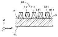
도 4 및 도 5는, 투명 기재(9)상의 패턴(81)의 일례를 도시하는 단면도이다. 본 실시 형태에 있어서의 패턴(81)은, 금속으로 형성되는 배선 패턴이다. 터치 패널에 이용되는 투명 기재(9)에서는, 패턴(81)은 상기 터치 패널의 외측 가장자리부에 상당하는 영역에 형성되고, 중앙부에 상당하는 영역에 ITO 등으로 형성되는 투명 전극 패턴과 접속된다. 즉, 패턴(81)은, 투명 전극 패턴과 접속되는 불투명 패턴이다. 패턴(81)은 복수의 패턴 요소(811)를 가진다. 각 패턴 요소(811)의 폭은, 예를 들어 10~30마이크로미터(μm)이다. 도 4 및 도 5, 및, 후술의 도 6 및 도 7의 상단에서는, 이상적인 패턴 요소(811)의 외형을 이점 쇄선으로 나타내고 있다. 도 4의 패턴 요소(811)에서는 끝부분이 가늘어져 있고(밑이 좁아져 있고), 도 5의 패턴 요소(811)에서는 끝부분이 두꺼워져 있다(퍼져 있다).4 and 5 are cross-sectional views showing an example of the
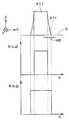
도 6 및 도 7은, 상면 반사 화상 및 하면 반사 화상에 있어서의 휘도값의 변화를 도시하는 도이다. 도 6 및 도 7의 상단은 각각 도 4 및 도 5의 일부의 패턴 요소(811)를 나타내고, 중단은 상기 패턴 요소(811)를 나타내는 상면 반사 화상에 있어서 X방향(에 대응하는 방향)에 늘어선 화소의 휘도값의 변화를 나타내며, 하단은 상기 패턴 요소(811)를 나타내는 하면 반사 화상에 있어서 X방향으로 늘어선 화소의 휘도값의 변화를 나타낸다.Figs. 6 and 7 are diagrams showing changes in the luminance value in the top-side reflection image and the bottom-reflection image, respectively. 6 and 7 show the
검사부(12)에서는, 상면 반사 화상, 하면 반사 화상 및 투과 화상에 의거하여 패턴의 검사 결과가 취득된다(단계 S15). 상세하게는, 하나의 검사 처리로서 상면 반사 화상과 하면 반사 화상이 비교된다. 패턴 요소(811)의 끝부분이 가늘어져 있는 도 6의 상단의 예에서는, 중단에 나타내는 상면 반사 화상에 있어서 패턴 요소(811)의 상면(즉, 투명 기재(9)와는 반대측을 향하는 면)에 대응하는 범위에 포함되는 화소의 휘도값이 높아지는데 비해, 하단에 나타내는 하면 반사 화상에서는 패턴 요소(811)의 하면(즉, 투명 기재(9)와 접하는 면)에 대응하는 범위에 포함되는 화소의 휘도값이 높아진다. 따라서, 검사부(12)에서는, 상면 반사 화상이 나타내는 패턴 요소(811)의 상면의 에지 위치와 하면 반사 화상이 나타내는 패턴 요소(811)의 하면의 에지 위치의 차를 취득함으로써, 패턴 요소(811)의 끝부분에 있어서의 가늘어짐량(W1)이 구해진다. 본 실시 형태에서는, 상면 반사 화상과 하면 반사 화상의 차분 화상을 구함으로써, 가늘어짐량(W1)이 취득된다(도 7의 예에 있어서 동일).In the
패턴 요소(811)의 끝부분이 두꺼워져 있는 도 7의 상단의 예에서는, 도 6의 예와 마찬가지로, 중단에 나타내는 상면 반사 화상에 있어서 패턴 요소(811)의 상면에 대응하는 범위에 포함되는 화소의 휘도값이 높아지는데 비해, 하단에 나타내는 하면 반사 화상에서는 패턴 요소(811)의 범위에 포함되는 화소의 휘도값이 높아진다. 따라서, 검사부(12)에서는, 상면 반사 화상이 나타내는 패턴 요소(811)의 상면의 에지 위치와 하면 반사 화상이 나타내는 패턴 요소(811)의 하면의 에지 위치의 차를 취득함으로써, 패턴 요소(811)의 끝부분에 있어서의 두꺼워짐량(W2)이 구해진다.In the upper example of Fig. 7 where the end portion of the
가늘어짐량(W1) 또는 두꺼워짐량(W2)은 소정의 역치와 비교되어, 상기 역치 이상인 경우에, 패턴 요소(811)의 끝부분에 있어서 허용 범위를 초과하여 가늘어지거나 또는 두꺼워지고 있는 것이, 패턴의 검사 결과로서 표시부(도시 생략)에 표시된다. 실제로는, 상면 반사 화상도 표시부에 표시되고, 조작자가 상면 반사 화상을 참조함으로써, 패턴 요소(811)의 상면 상태(상면이 거친 상태 등)가 확인된다. 또한, 역치는 가늘어짐량과 두꺼워짐량으로 개별적으로 설정되어도 된다.The taper amount W1 or the thickening amount W2 is compared with a predetermined threshold value so that it becomes thinner or thicker beyond the permissible range at the end of the
검사부(12)에 있어서의 다른 검사 처리에서는, 투과 화상에 의거하여 패턴 요소(811)의 상면에 있어서의 오목부의 유무가 검출된다. 여기서, 패턴 요소(811)의 상면에 있어서의 오목부는, 디쉬 다운으로도 불리고, 오목부가 발생한 부분에 있어 패턴 요소(811)의 두께가 작아진다. 수백 나노미터(nm)의 두께의 패턴 요소(811)에서는, 오목부가 발생한 부분에 있어서의 패턴 요소(811)의 두께가, 예를 들어 70nm 이하가 되고, 제2 광원부(332)로부터의 적색의 광에서는, 수백nm의 두께의 금속막의 투과율이 거의 0인데 비해, 70nm 이하의 두께의 금속막의 투과율은 비교적 높아진다.In the other inspection processing in the
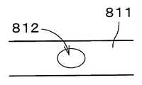
예를 들어, 도 8에 도시하는 패턴 요소(811)에 있어서 세선으로 둘러싸는 영역(812)(이하, 「디쉬 다운 영역(812)」이라고 한다)에 오목부가 발생되어 있는 경우, 도 9에 도시하는 바와 같이, 투과 화상에 있어서 패턴 요소(811)를 나타내는 영역의 대부분에서는 휘도값이 낮아(어두워)지지만, 디쉬 다운 영역(812)을 나타내는 영역에서는 휘도값이 주위보다 높아(밝아)진다. 도 9에서는, 평행 사선의 간격을 바꿈으로써 휘도값의 차이를 나타내고 있고, 평행 사선의 간격이 좁을수록 휘도값이 낮은 것을 나타낸다.For example, when a concave portion is generated in a
또, 제1 광원부(331)로부터의 청색의 광에서는, 수백nm의 두께의 금속막(예를 들어, Cu, Ag 등) 및 70nm 이하의 두께의 금속막의 투과율은 더불어 거의 0이지만, 디쉬 다운에 의해 반사광의 방향이 변화하기 때문에, 디쉬 다운 영역이 약간 어두워진다. 도 10에 도시하는 바와 같이, 상면 반사 화상에 있어서, 패턴 요소(811)의 상면을 나타내는 영역의 거의 전체의 휘도값이 높아(밝아)지지만, 디쉬 다운 영역은 약간 어두워진다. 따라서, 검사부(12)에서는, 투과 화상과 상면 반사 화상을 소정의 수법으로 합성함으로써, 디쉬 다운 영역(812)을 나타내는 화상을 취득하는 것, 즉, 디쉬 다운 영역(812)을 검출하는 것이 용이해진다. 소정의 면적 이상의 디쉬 다운 영역(812)이 검출돤 경우에는, 패턴 요소(811)의 상면에 오목부가 발생되어 있는 것이, 패턴의 검사 결과로서 표시부에 표시된다. 또한, 디쉬 다운 영역(812)의 화상이 표시부에 표시되어도 된다.In the blue light from the first
이상과 같이 하여, 상면 반사 화상, 하면 반사 화상 및 투과 화상에 의거하여 패턴의 검사 결과가 취득된다. 단계 S12~S15의 처리는, 투명 기재(9)가 일정한 거리만큼 이동할 때마다 반복 실행된다. 투명 기재(9)의 전체에 대한 검사가 완료하면, 제1 광원부(331) 및 제2 광원부(332)가 소등됨과 더불어, 투명 기재(9)의 이동이 정지되고, 검사가 종료한다(단계 S16). 또한, 검사부(12)에서는, 가늘어짐량(W1)이나 두꺼워짐량(W2), 혹은, 디쉬 다운 영역(812)의 면적 등이, 패턴의 검사 결과로서 취급되어도 된다. 환언하면, 패턴 검사 장치(1)는, 패턴의 두꺼워짐량 또는 가늘어짐량이나, 디쉬 다운 영역(812)의 면적 등을 측정하는 측정 장치로서 파악되어도 된다.As described above, the inspection result of the pattern is acquired based on the top-side reflection image, the bottom-side reflection image, and the transmission image. The processing of steps S12 to S15 is repeated every time the
이상으로 설명한 바와 같이, 패턴 검사 장치(1)에서는, 한쪽의 주면(만)에 패턴(81)이 형성된 투명 기재(9)에 대해, 제1 화상 취득부(301)에 의해 패턴(81)의 상면으로부터의 반사광에 의거하는 상면 반사 화상이 취득되고, 제2 화상 취득부(302)에 의해 패턴(81)의 하면으로부터의 반사광에 의거하는 하면 반사 화상이 취득된다. 그리고, 검사부(12)에 있어서, 상면 반사 화상과 하면 반사 화상에 의거하여 패턴(81)의 검사 결과가 취득된다. 이에 의해, 패턴 요소(811)의 끝부분에 있어서의 두꺼워짐이나 가늘어짐을 용이하게 검사할 수 있다.As described above, in the
또, 제1 화상 취득부(301)가, 제2 수광부(332)로부터의 광이 제1 수광부(341)에 입사하는 것을 방지하는 다이크로익 미러(315)를 가지고, 제2 화상 취득부(302)가, 제1 광원부(331)로부터의 광이 제2 수광부(342)에 입사하는 것을 방지하는 밴드 패스 필터(325)를 가진다. 이에 의해, 상면 반사 화상과 하면 반사 화상을 동시에 취득하는 것이 용이하게 가능해지고, 투명 기재(9)상의 패턴(81)의 검사를 고속으로 행하는 것이 실현된다.The first
또한, 패턴 검사 장치(1)에서는, 제2 광원부(332)로부터 출사되고, 투명 기재(9)를 투과한 광을 수광하여 투과 화상을 취득하는 제3 화상 취득부(303)가 더 설치된다. 이에 의해, 패턴 요소(811)의 상면에 있어서의 오목부를 검출하는 것이 용이해진다.The
도 11은, 본 발명의 다른 실시 형태에 따른 패턴 검사 장치(1)에 있어서의 화상 취득 유닛(3a)의 구성을 도시하는 도이다. 도 11의 화상 취득 유닛(3a)에서는, 도 2의 화상 취득 유닛(3)에 있어서의 다이크로익 미러(315), 제3 수광부(343) 및 밴드 패스 필터(325)가 생략되고, 제1 수광부(341)가 제3 수광부(343)의 위치에 배치된다. 다른 구성은, 도 2의 화상 취득 유닛(3)과 마찬가지로, 같은 구성에 같은 부호를 붙인다.11 is a diagram showing the configuration of the image acquisition unit 3a in the
화상 취득 유닛(3a)에서는, 제1 광원부(331)에 의해 제1 주면(91)상에 조사된 유닛(3a) 중, 패턴(81)으로부터의 반사광이 대물 렌즈(313), 하프 미러(312) 및 결상 렌즈(314)를 개재하여 제1 수광부(341)로 인도된다. 또, 제1 광원부(331)로부터의 광의 투명 기재(9)로부터의 투과광이, 대물 렌즈(323), 하프 미러(322) 및 결상 렌즈(324)를 개재하여 제2 수광부(342)로 인도된다. 한편, 제2 광원부(332)에 의해 제2 주면(92)상에 조사된 광 중, 패턴(81)의 하면으로부터의 반사광이 대물 렌즈(323), 하프 미러(322) 및 결상 렌즈(324)를 개재하여 제2 수광부(342)로 인도된다. 또, 제2 광원부(332)로부터의 광의 투명 기재(9)로부터의 투과광이 대물 렌즈(313), 하프 미러(312) 및 결상 렌즈(314)를 개재하여 제1 수광부(341)로 인도된다. 이와 같이, 제1 수광부(341)에서는, 제1 광원부(331)로부터의 광의 패턴(81)으로부터의 반사광과, 제2 광원부(332)로부터의 광의 투명 기재(9)로부터의 투과광이 수광 가능하다. 또, 제2 수광부(342)에서는, 제2 광원부(332)로부터의 광의 패턴(81)으로부터의 반사광과, 제1 광원부(331)로부터의 광의 투명 기재(9)로부터의 투과광이 수광 가능하다.The reflected light from the
화상 취득 유닛(3a)을 가지는 패턴 검사 장치(1)에서는, 이동 기구(2)에 의해 투명 기재(9)를 이동 방향으로 연속적으로 이동하면서, 제어부(11)(도 1 참조)의 제어에 의해, 제1 광원부(331)와 제2 광원부(332)가 교호로 반복하여 점등한다(즉, 제1 광원부(331)의 점등 및 제2 광원부(332)의 소등과, 제1 광원부(331)의 소등 및 제2 광원부(332)의 점등이 반복된다). 이에 의해, 제1 수광부(341)에서는, 패턴(81)의 상면으로부터의 반사광에 의거하는 상면 반사 화상의 라인 화상과, 투명 기재(9)로부터의 투과광에 의거하는 제1 투과 화상의 라인 화상이 교호로 취득된다. 또, 제2 수광부(342)에서는, 패턴(81)의 하면으로부터의 반사광에 의거하는 하면 반사 화상의 라인 화상과, 투명 기재(9)로부터의 투과광에 의거하는 제2 투과 화상의 라인 화상이 교호로 취득된다. 그리고, 검사부(12)에서는, 상기 처리예와 마찬가지로, 상면 반사 화상, 하면 반사 화상, 제1 투과 화상 및 제2 투과 화상에 의거하여 패턴의 검사 결과가 출력된다.The
또한, 화상 취득 유닛(3a)에서는, 상면 반사 화상을 취득하는 제1 화상 취득부(301)와, 제1 투과 화상을 취득하는 제3 화상 취득부(303)의 사이에 있어서, 제1 광학계(31)의 일부에 더해, 제1 수광부(341)가 공유된다. 제2 수광부(342)에서는, 반드시 제2 투과 화상이 취득될 필요는 없다.In the image acquisition unit 3a, the first
이상으로 설명한 바와 같이, 화상 취득 유닛(3a)을 가지는 패턴 검사 장치(1)에서는, 이동 기구(2)에 의해 투명 기재(9)를 연속적으로 이동하면서, 제1 광원부(331)와 제2 광원부(332)를 교호로 점등시킴으로써, 하나의 제1 수광부(341)를 이용하여 반사광에 의거하는 상면 반사 화상과, 투과광에 의거하는 투과 화상을 취득하는 것이 실현된다. 이에 의해, 패턴 검사 장치(1)에 있어서의 부품점수를 삭감할 수 있다. 또한, 도 11의 패턴 검사 장치(1)에서는, 제1 광원부(331)가 적색의 파장대의 광을 출사해도 된다.As described above, in the
상기 패턴 검사 장치(1)는 여러 가지 변형이 가능하다. 상기 실시 형태에서는, 제2 광원부(332)가 적색의 파장대의 광을 출사하지만, 적색에서 적외까지의 파장 범위에 포함되는 임의의 파장대(예를 들어, 근적외 파장대)의 광을 출사해도 된다. 이에 의해, 패턴 요소(811)의 상면에 있어서의 오목부를 용이하게 검출하는 것이 가능해진다. 또, 도 2의 제3 수광부(343)가 투명 기재(9)의 (-Z)측에 배치되고, 제1 광원부(331)가 상기 파장 범위에 포함되는 임의의 파장대의 광을 출사해도 된다. 이 경우, 제1 광원부(331)로부터 출사되고, 투명 기재(9)를 투과한 광이 제3 수광부(343)에서 수광되고, 투과 화상이 취득된다. 패턴 검사 장치(1)에 있어서의 검사 대상의 패턴의 종류에 의해서는, 제1 광원부(331) 및 제2 광원부(332)가 다른 파장대의 광을 출사해도 된다. 제1 광원부(331) 및 제2 광원부(332)는, LED 이외의 발광 소자나 램프를 광원으로서 가지고 있어도 된다.The
또, 화상 취득 유닛(3)의 설계에 의해서는, 제2 광원부(332)로부터의 광이 제1 수광부(341)에 입사하는 것을 방지하는 밴드 패스 필터가 제1 광학계(31)에 설치되고, 제1 광원부(331)로부터의 광이 제2 수광부(342)에 입사하는 것을 방지하는 다이크로익 미러가 제2 광학계(32)에 설치되어도 된다. 또, 특정의 파장대의 광만을 투과하는 또는 차폐하는 다른 종류의 광학 소자가 이용되어도 된다. 패턴 검사 장치(1)에 있어서 상면 반사 화상과 하면 반사 화상을 동시에 취득하려면, 제1 광원부(331)가, 제1 파장대의 광을 출사하고, 제2 광원부(332)가, 제1 파장대와 상이한 제2 파장대의 광을 출사하며, 제1 화상 취득부(301)가, 제2 파장대의 광이 제1 수광부(341)에 입사하는 것을 방지하는 광학 소자를 가지고, 제2 화상 취득부(302)가, 제1 파장대의 광이 제2 수광부(342)에 입사하는 것을 방지하는 광학 소자를 가지는 것이 중요해진다.According to the design of the
제1 수광부(341), 제2 수광부(342) 및 제3 수광부(343)는, 수광 소자가 2차원에 배열된 에리어 센서여도 된다. 이 경우에, 이동 기구가 투명 기재(9)를 단속적으로 이동 방향으로 이동(단계 이동)함으로써, 상면 반사 화상, 하면 반사 화상 및 투과 화상이 취득되어도 된다. 또, 도 11의 패턴 검사 장치(1)에 있어서, 투명 기재(9)를 단속적으로 이동하면서 투명 기재(9)의 각 정지 위치에서 제1 광원부(331) 및 제2 광원부(332)를 교호로 점등함으로써, 상면 반사 화상, 하면 반사 화상, 제1 투과 화상 및 제2 투과 화상이 고정밀도로 취득되어도 된다.The first
제1 광원부(331) 및 제2 광원부(332)의 배치, 및, 제1 수광부(341), 제2 수광부(342) 및 제3 수광부(343)의 배치는, 제1 광학계(31) 및 제2 광학계(32)의 구성에 맞추어 적당히 변경되어도 된다.The arrangement of the first
패턴 검사 장치(1)에서는, 화상 취득 유닛(3, 3a)을 투명 기재(9)에 대해 이동 방향으로 이동하는 이동 기구가 설치되어도 된다. 또, 투명 기재(9)를 투명한 스테이지상에 올려놓고, 상기 스테이지를 화상 취득 유닛에 대해 상대적으로 이동 방향으로 이동함으로써, 상면 반사 화상 및 투과 화상이 취득되어도 된다.In the
패턴 검사 장치(1)에 있어서의 검사의 대상물은, 필름형상의 투명 기재(9)에 형성된 패턴 이외에, 유리 등의 판형상의 투명 기재에 형성된 패턴이어도 된다. 투명 기재는, 터치 패널 이외에 이용되어도 된다. 또, 투명 기재상의 패턴은, 불투명하다면, 예를 들어 포토레지스트로 형성된 패턴 등이어도 된다.An object to be inspected in the
상기 실시 형태 및 각 변형예에 있어서의 구성은, 서로 모순되지 않는 한 적당히 조합해도 된다.The configurations of the above-described embodiment and the modified examples may be appropriately combined as long as they do not contradict each other.
발명을 상세하게 묘사하여 설명했으나, 기술된 설명은 예시로서 한정적인 것은 아니다. 따라서, 본 발명의 범위를 일탈하지 않는 한, 다수의 변형이나 양태가 가능하다고 할 수 있다.While the invention has been illustrated and described in detail, the description provided is by way of example and not of limitation. Therefore, many modifications and variations are possible without departing from the scope of the present invention.
1 패턴 검사 장치
9 투명 기재
12 검사부
81 패턴
91 제1 주면
92 제2 주면
301 제1 화상 취득부
302 제2 화상 취득부
303 제3 화상 취득부
315 다이크로익 미러
325 밴드 패스 필터
331 제1 광원부
332 제2 광원부
341 제1 수광부
342 제2 수광부
343 제3 수광부
811 패턴 요소1 pattern inspection device
9 Transparent substrate
12 Inspector
81 patterns
91 First week
92 Second Week
301 First image acquisition unit
302 Second image acquisition unit
303 Third image acquisition unit
315 Dichroic mirror
325 bandpass filter
331 First light source
332 Second light source part
341 First light receiving portion
342 Second light receiving portion
343 Third light receiving section
811 Pattern elements
Claims (10)
Translated fromKorean판형상 또는 필름형상의 투명 기재에 있어서 패턴이 형성된 한쪽의 주면에 제1 광원부로부터의 광을 조사하고, 상기 패턴의 상면으로부터의 상기 광의 반사광을 제1 수광부에서 수광하여 상면 반사 화상을 취득하는 제1 화상 취득부와,
상기 투명 기재의 다른쪽의 주면에 제2 광원부로부터의 광을 조사하고, 상기 한쪽의 주면에 접하는 상기 패턴의 하면으로부터의 상기 광의 반사광을 제2 수광부에서 수광하여 하면 반사 화상을 취득하는 제2 화상 취득부와,
상기 상면 반사 화상과 상기 하면 반사 화상에 의거하여 상기 패턴의 검사 결과를 취득하는 검사부를 구비하는, 패턴 검사 장치.A pattern inspection apparatus for inspecting a pattern on a transparent substrate,
A transparent substrate of a plate shape or a film shape is irradiated with light from the first light source part on one principal surface on which a pattern is formed and the reflected light of the light from the upper surface of the pattern is received by the first light receiving part, One image acquisition unit,
The second light receiving portion irradiates the other main surface of the transparent substrate with the light from the second light source portion and the reflected light from the lower surface of the pattern contacting the one main surface is received by the second light receiving portion, An acquisition unit,
And an inspection unit that acquires inspection results of the pattern on the basis of the top reflection image and the bottom reflection image.
상기 제1 광원부가, 제1 파장대의 광을 출사하고,
상기 제2 광원부가, 상기 제1 파장대와 상이한 제2 파장대의 광을 출사하며,
상기 제1 화상 취득부가, 상기 제2 파장대의 광이 상기 제1 수광부에 입사하는 것을 방지하는 광학 소자를 가지고,
상기 제2 화상 취득부가, 상기 제1 파장대의 광이 상기 제2 수광부에 입사하는 것을 방지하는 광학 소자를 가지며,
상기 상면 반사 화상과 상기 하면 반사 화상이 동시에 취득되는, 패턴 검사 장치.The method according to claim 1,
Wherein the first light source unit emits light of a first wavelength band,
The second light source unit emits light of a second wavelength band different from the first wavelength band,
The first image acquisition section has an optical element for preventing light of the second wavelength range from entering the first light receiving section,
The second image capturing section has an optical element for preventing light of the first wavelength range from entering the second light receiving section,
Wherein the upper reflection image and the lower reflection image are acquired simultaneously.
상기 제1 광원부 또는 상기 제2 광원부로부터 출사되고, 상기 투명 기재를 투과한 광을 수광하여 투과 화상을 취득하는 제3 화상 취득부를 더 구비하는, 패턴 검사 장치.The method according to claim 1,
Further comprising: a third image acquisition unit that acquires a transmission image, which is emitted from the first light source unit or the second light source unit and receives light transmitted through the transparent substrate.
상기 제1 광원부 또는 상기 제2 광원부로부터 출사되고, 상기 투명 기재를 투과한 광을 수광하여 투과 화상을 취득하는 제3 화상 취득부를 더 구비하는, 패턴 검사 장치.The method of claim 2,
Further comprising: a third image acquisition unit that acquires a transmission image, which is emitted from the first light source unit or the second light source unit and receives light transmitted through the transparent substrate.
상기 패턴이 금속으로 형성되는, 패턴 검사 장치.The method according to any one of claims 1 to 4,
Wherein the pattern is formed of a metal.
a) 판형상 또는 필름형상의 투명 기재에 있어서 패턴이 형성된 한쪽의 주면에 제1 광원부로부터의 광을 조사하고, 상기 패턴의 상면으로부터의 상기 광의 반사광을 제1 수광부에서 수광하여 제1 화상 취득부에서 상면 반사 화상을 취득하는 공정과,
b) 상기 투명 기재의 다른쪽의 주면에 제2 광원부로부터의 광을 조사하고, 상기 한쪽의 주면에 접하는 상기 패턴의 하면으로부터의 상기 광의 반사광을 제2 수광부에서 수광하여 제2 화상 취득부에서 하면 반사 화상을 취득하는 공정과,
c) 상기 상면 반사 화상과 상기 하면 반사 화상에 의거하여 상기 패턴의 검사 결과를 취득하는 공정을 구비하는, 패턴 검사 방법.A pattern inspection method for inspecting a pattern on a transparent substrate using a pattern inspection apparatus,
a) In a plate-like or film-shaped transparent substrate, light from the first light source section is irradiated onto one principal surface on which a pattern is formed, light reflected by the upper surface of the pattern is received by the first light receiving section, A step of acquiring a top-
b) The light from the second light source portion is irradiated to the other principal surface of the transparent substrate, and the reflected light from the lower surface of the pattern contacting the one main surface is received by the second light receiving portion, A step of obtaining a reflected image,
and (c) acquiring an inspection result of the pattern on the basis of the top reflection image and the bottom reflection image.
상기 제1 광원부가, 제1 파장대의 광을 출사하고,
상기 제2 광원부가, 상기 제1 파장대와 상이한 제2 파장대의 광을 출사하며,
상기 제1 화상 취득부가, 상기 제2 파장대의 광이 상기 제1 수광부에 입사하는 것을 방지하는 광학 소자를 가지고,
상기 제2 화상 취득부가, 상기 제1 파장대의 광이 상기 제2 수광부에 입사하는 것을 방지하는 광학 소자를 가지며,
상기 상면 반사 화상과 상기 하면 반사 화상이 동시에 취득되는, 패턴 검사 방법.The method of claim 6,
Wherein the first light source unit emits light of a first wavelength band,
The second light source unit emits light of a second wavelength band different from the first wavelength band,
The first image acquisition section has an optical element for preventing light of the second wavelength range from entering the first light receiving section,
The second image capturing section has an optical element for preventing light of the first wavelength range from entering the second light receiving section,
Wherein the upper surface reflection image and the lower surface reflection image are simultaneously acquired.
상기 제1 광원부 또는 상기 제2 광원부로부터 출사되고, 상기 투명 기재를 투과한 광을 제3 화상 취득부에서 수광하여 투과 화상을 취득하는 공정을 더 구비하는, 패턴 검사 방법.The method of claim 6,
Further comprising a step of receiving light transmitted from the first light source unit or the second light source unit and transmitted through the transparent substrate by a third image acquisition unit to acquire a transmission image.
상기 제1 광원부 또는 상기 제2 광원부로부터 출사되고, 상기 투명 기재를 투과한 광을 제3 화상 취득부에서 수광하여 투과 화상을 취득하는 공정을 더 구비하는, 패턴 검사 방법.The method of claim 7,
Further comprising a step of receiving light transmitted from the first light source unit or the second light source unit and transmitted through the transparent substrate by a third image acquisition unit to acquire a transmission image.
상기 패턴이 금속으로 형성되는, 패턴 검사 방법.The method according to any one of claims 6 to 9,
Wherein the pattern is formed of a metal.
Applications Claiming Priority (2)
| Application Number | Priority Date | Filing Date | Title |
|---|---|---|---|
| JPJP-P-2013-028216 | 2013-02-15 | ||
| JP2013028216AJP6085188B2 (en) | 2013-02-15 | 2013-02-15 | Pattern inspection device |
Publications (2)
| Publication Number | Publication Date |
|---|---|
| KR20140103026Atrue KR20140103026A (en) | 2014-08-25 |
| KR101577119B1 KR101577119B1 (en) | 2015-12-11 |
Family
ID=51309231
Family Applications (1)
| Application Number | Title | Priority Date | Filing Date |
|---|---|---|---|
| KR1020130161427AExpired - Fee RelatedKR101577119B1 (en) | 2013-02-15 | 2013-12-23 | Pattern inspection apparatus and pattern inspection method |
Country Status (4)
| Country | Link |
|---|---|
| JP (1) | JP6085188B2 (en) |
| KR (1) | KR101577119B1 (en) |
| CN (1) | CN103995008A (en) |
| TW (1) | TWI534424B (en) |
Cited By (1)
| Publication number | Priority date | Publication date | Assignee | Title |
|---|---|---|---|---|
| KR101879735B1 (en)* | 2017-03-15 | 2018-07-18 | (주)넥셀 | Method and apparatus for automatic generating training data and self-learning apparatus and method using the same |
Families Citing this family (6)
| Publication number | Priority date | Publication date | Assignee | Title |
|---|---|---|---|---|
| KR101712924B1 (en)* | 2015-02-03 | 2017-03-08 | 성우테크론 주식회사 | apparatus for optical inspection |
| JP6496159B2 (en)* | 2015-02-23 | 2019-04-03 | 株式会社Screenホールディングス | Pattern inspection apparatus and pattern inspection method |
| JP6450697B2 (en)* | 2016-03-22 | 2019-01-09 | Ckd株式会社 | Board inspection equipment |
| KR102037395B1 (en)* | 2017-09-25 | 2019-10-28 | 동우 화인켐 주식회사 | Transmissive optical inspection device and method of detecting film defect using the same |
| JP2021096112A (en)* | 2019-12-16 | 2021-06-24 | コニカミノルタ株式会社 | Inspection device for transparent body |
| KR102267705B1 (en)* | 2020-09-17 | 2021-06-22 | 주식회사 티에스아이코리아 | Inspection apparatus for chip on film |
Family Cites Families (12)
| Publication number | Priority date | Publication date | Assignee | Title |
|---|---|---|---|---|
| JPS53102792A (en)* | 1977-02-21 | 1978-09-07 | Hitachi Ltd | Simultaneous inspecting apparatus of inside and outside of body to be inspected |
| JP3418054B2 (en)* | 1996-02-16 | 2003-06-16 | 三井金属鉱業株式会社 | Wiring pattern line width measurement device |
| JP3378795B2 (en)* | 1998-03-27 | 2003-02-17 | シャープ株式会社 | Display device inspection apparatus and inspection method |
| JP4227272B2 (en)* | 1999-08-11 | 2009-02-18 | 株式会社エヌテック | Inspection device for articles using light of different wavelengths |
| JP2001305074A (en)* | 2000-04-19 | 2001-10-31 | Dainippon Printing Co Ltd | Inspection method and apparatus for plate-like work |
| JP4304690B2 (en)* | 2002-12-27 | 2009-07-29 | 国際技術開発株式会社 | Tape member inspection device |
| JP4403777B2 (en)* | 2003-11-07 | 2010-01-27 | ウシオ電機株式会社 | Wiring pattern inspection apparatus and method |
| JP2008026212A (en)* | 2006-07-24 | 2008-02-07 | Ushio Inc | Pattern inspection device |
| CN101887030A (en)* | 2009-05-15 | 2010-11-17 | 圣戈本玻璃法国公司 | Method and system for detecting defects on the surface and/or inside of a transparent substrate |
| KR101240564B1 (en)* | 2009-09-02 | 2013-03-14 | 아주하이텍(주) | Optical inspection apparatus and method of inspecting using the same |
| CN101806751B (en)* | 2010-03-02 | 2012-01-11 | 清华大学 | Double-light source transmission reflection imaging detection device for lint impurities |
| JP5585301B2 (en) | 2010-08-24 | 2014-09-10 | オムロン株式会社 | Visual inspection system for sheets |
- 2013
- 2013-02-15JPJP2013028216Apatent/JP6085188B2/ennot_activeExpired - Fee Related
- 2013-12-23KRKR1020130161427Apatent/KR101577119B1/ennot_activeExpired - Fee Related
- 2013-12-24TWTW102147906Apatent/TWI534424B/ennot_activeIP Right Cessation
- 2014
- 2014-02-17CNCN201410053709.8Apatent/CN103995008A/enactivePending
Cited By (1)
| Publication number | Priority date | Publication date | Assignee | Title |
|---|---|---|---|---|
| KR101879735B1 (en)* | 2017-03-15 | 2018-07-18 | (주)넥셀 | Method and apparatus for automatic generating training data and self-learning apparatus and method using the same |
Also Published As
| Publication number | Publication date |
|---|---|
| JP6085188B2 (en) | 2017-02-22 |
| CN103995008A (en) | 2014-08-20 |
| TW201447286A (en) | 2014-12-16 |
| JP2014157085A (en) | 2014-08-28 |
| TWI534424B (en) | 2016-05-21 |
| KR101577119B1 (en) | 2015-12-11 |
Similar Documents
| Publication | Publication Date | Title |
|---|---|---|
| KR101577119B1 (en) | Pattern inspection apparatus and pattern inspection method | |
| KR101588937B1 (en) | Pattern inspection apparatus and pattern inspection method | |
| US9110035B2 (en) | Method and system for detecting defects of transparent substrate | |
| WO2018088423A1 (en) | Optical inspection device | |
| US10887500B2 (en) | Optical inspection system | |
| WO2010097055A1 (en) | System and method for detecting defects of substrate | |
| WO2003064973A1 (en) | Three-dimensional measuring instrument, filter striped plate, and illuminating means | |
| JP2012042297A (en) | Imaging optical inspection apparatus | |
| CN101762611A (en) | Wiring pattern checking device | |
| JP6487617B2 (en) | Defect inspection method and defect inspection apparatus for microlens array | |
| KR20120031835A (en) | Apparatus for inspecting defects | |
| JP2012242268A (en) | Inspection device and inspection method | |
| JP4808072B2 (en) | Filter checkered plate, three-dimensional measuring device and illumination means | |
| JP5787668B2 (en) | Defect detection device | |
| KR101015808B1 (en) | Bonding electrode line width measuring apparatus and method | |
| JP2012068211A (en) | Distortion inspection device for sheet member and distortion inspection method for sheet member | |
| JP2004212353A (en) | Optical inspection apparatus | |
| TW201710664A (en) | Defect inspection device controls the main light source module relative to irradiation angle and irradiation position on the article under inspection | |
| WO2021090827A1 (en) | Inspection device | |
| JP2016125968A (en) | Check device and method for checking | |
| KR20160082392A (en) | Illumination unit and inspection apparatus | |
| KR20220011970A (en) | Apparatus and method for measuring micro lens used | |
| CN111795643A (en) | Apparatus for determining chip orientation | |
| JP2019138696A (en) | Visual inspection method and visual inspection device |
Legal Events
| Date | Code | Title | Description |
|---|---|---|---|
| A201 | Request for examination | ||
| PA0109 | Patent application | St.27 status event code:A-0-1-A10-A12-nap-PA0109 | |
| PA0201 | Request for examination | St.27 status event code:A-1-2-D10-D11-exm-PA0201 | |
| PG1501 | Laying open of application | St.27 status event code:A-1-1-Q10-Q12-nap-PG1501 | |
| PN2301 | Change of applicant | St.27 status event code:A-3-3-R10-R13-asn-PN2301 St.27 status event code:A-3-3-R10-R11-asn-PN2301 | |
| D13-X000 | Search requested | St.27 status event code:A-1-2-D10-D13-srh-X000 | |
| D14-X000 | Search report completed | St.27 status event code:A-1-2-D10-D14-srh-X000 | |
| E902 | Notification of reason for refusal | ||
| PE0902 | Notice of grounds for rejection | St.27 status event code:A-1-2-D10-D21-exm-PE0902 | |
| E13-X000 | Pre-grant limitation requested | St.27 status event code:A-2-3-E10-E13-lim-X000 | |
| P11-X000 | Amendment of application requested | St.27 status event code:A-2-2-P10-P11-nap-X000 | |
| P13-X000 | Application amended | St.27 status event code:A-2-2-P10-P13-nap-X000 | |
| E701 | Decision to grant or registration of patent right | ||
| PE0701 | Decision of registration | St.27 status event code:A-1-2-D10-D22-exm-PE0701 | |
| GRNT | Written decision to grant | ||
| PR0701 | Registration of establishment | St.27 status event code:A-2-4-F10-F11-exm-PR0701 | |
| PR1002 | Payment of registration fee | St.27 status event code:A-2-2-U10-U11-oth-PR1002 Fee payment year number:1 | |
| PG1601 | Publication of registration | St.27 status event code:A-4-4-Q10-Q13-nap-PG1601 | |
| LAPS | Lapse due to unpaid annual fee | ||
| PC1903 | Unpaid annual fee | St.27 status event code:A-4-4-U10-U13-oth-PC1903 Not in force date:20181208 Payment event data comment text:Termination Category : DEFAULT_OF_REGISTRATION_FEE | |
| PC1903 | Unpaid annual fee | St.27 status event code:N-4-6-H10-H13-oth-PC1903 Ip right cessation event data comment text:Termination Category : DEFAULT_OF_REGISTRATION_FEE Not in force date:20181208 |