KR20140102782A - Blade for transferring wafer and wafer transferring apparatus having the same - Google Patents
Blade for transferring wafer and wafer transferring apparatus having the sameDownload PDFInfo
- Publication number
- KR20140102782A KR20140102782AKR1020130015605AKR20130015605AKR20140102782AKR 20140102782 AKR20140102782 AKR 20140102782AKR 1020130015605 AKR1020130015605 AKR 1020130015605AKR 20130015605 AKR20130015605 AKR 20130015605AKR 20140102782 AKR20140102782 AKR 20140102782A
- Authority
- KR
- South Korea
- Prior art keywords
- wafer
- branch
- wafer transfer
- transfer blade
- blade
- Prior art date
- Legal status (The legal status is an assumption and is not a legal conclusion. Google has not performed a legal analysis and makes no representation as to the accuracy of the status listed.)
- Withdrawn
Links
Images


Classifications
- H—ELECTRICITY
- H01—ELECTRIC ELEMENTS
- H01L—SEMICONDUCTOR DEVICES NOT COVERED BY CLASS H10
- H01L21/00—Processes or apparatus adapted for the manufacture or treatment of semiconductor or solid state devices or of parts thereof
- H01L21/67—Apparatus specially adapted for handling semiconductor or electric solid state devices during manufacture or treatment thereof; Apparatus specially adapted for handling wafers during manufacture or treatment of semiconductor or electric solid state devices or components ; Apparatus not specifically provided for elsewhere
- H01L21/683—Apparatus specially adapted for handling semiconductor or electric solid state devices during manufacture or treatment thereof; Apparatus specially adapted for handling wafers during manufacture or treatment of semiconductor or electric solid state devices or components ; Apparatus not specifically provided for elsewhere for supporting or gripping
- H01L21/6838—Apparatus specially adapted for handling semiconductor or electric solid state devices during manufacture or treatment thereof; Apparatus specially adapted for handling wafers during manufacture or treatment of semiconductor or electric solid state devices or components ; Apparatus not specifically provided for elsewhere for supporting or gripping with gripping and holding devices using a vacuum; Bernoulli devices
- H—ELECTRICITY
- H01—ELECTRIC ELEMENTS
- H01L—SEMICONDUCTOR DEVICES NOT COVERED BY CLASS H10
- H01L21/00—Processes or apparatus adapted for the manufacture or treatment of semiconductor or solid state devices or of parts thereof
- H01L21/67—Apparatus specially adapted for handling semiconductor or electric solid state devices during manufacture or treatment thereof; Apparatus specially adapted for handling wafers during manufacture or treatment of semiconductor or electric solid state devices or components ; Apparatus not specifically provided for elsewhere
- H01L21/677—Apparatus specially adapted for handling semiconductor or electric solid state devices during manufacture or treatment thereof; Apparatus specially adapted for handling wafers during manufacture or treatment of semiconductor or electric solid state devices or components ; Apparatus not specifically provided for elsewhere for conveying, e.g. between different workstations
- H01L21/67739—Apparatus specially adapted for handling semiconductor or electric solid state devices during manufacture or treatment thereof; Apparatus specially adapted for handling wafers during manufacture or treatment of semiconductor or electric solid state devices or components ; Apparatus not specifically provided for elsewhere for conveying, e.g. between different workstations into and out of processing chamber
- H01L21/67742—Mechanical parts of transfer devices
- B—PERFORMING OPERATIONS; TRANSPORTING
- B25—HAND TOOLS; PORTABLE POWER-DRIVEN TOOLS; MANIPULATORS
- B25J—MANIPULATORS; CHAMBERS PROVIDED WITH MANIPULATION DEVICES
- B25J15/00—Gripping heads and other end effectors
- B25J15/06—Gripping heads and other end effectors with vacuum or magnetic holding means
- B25J15/0616—Gripping heads and other end effectors with vacuum or magnetic holding means with vacuum
- B25J15/0683—Details of suction cup structure, e.g. grooves or ridges
- H—ELECTRICITY
- H01—ELECTRIC ELEMENTS
- H01L—SEMICONDUCTOR DEVICES NOT COVERED BY CLASS H10
- H01L21/00—Processes or apparatus adapted for the manufacture or treatment of semiconductor or solid state devices or of parts thereof
- H01L21/67—Apparatus specially adapted for handling semiconductor or electric solid state devices during manufacture or treatment thereof; Apparatus specially adapted for handling wafers during manufacture or treatment of semiconductor or electric solid state devices or components ; Apparatus not specifically provided for elsewhere
- H01L21/683—Apparatus specially adapted for handling semiconductor or electric solid state devices during manufacture or treatment thereof; Apparatus specially adapted for handling wafers during manufacture or treatment of semiconductor or electric solid state devices or components ; Apparatus not specifically provided for elsewhere for supporting or gripping
- H01L21/687—Apparatus specially adapted for handling semiconductor or electric solid state devices during manufacture or treatment thereof; Apparatus specially adapted for handling wafers during manufacture or treatment of semiconductor or electric solid state devices or components ; Apparatus not specifically provided for elsewhere for supporting or gripping using mechanical means, e.g. chucks, clamps or pinches
- H01L21/68707—Apparatus specially adapted for handling semiconductor or electric solid state devices during manufacture or treatment thereof; Apparatus specially adapted for handling wafers during manufacture or treatment of semiconductor or electric solid state devices or components ; Apparatus not specifically provided for elsewhere for supporting or gripping using mechanical means, e.g. chucks, clamps or pinches the wafers being placed on a robot blade, or gripped by a gripper for conveyance
Landscapes
- Engineering & Computer Science (AREA)
- Physics & Mathematics (AREA)
- Condensed Matter Physics & Semiconductors (AREA)
- General Physics & Mathematics (AREA)
- Manufacturing & Machinery (AREA)
- Computer Hardware Design (AREA)
- Microelectronics & Electronic Packaging (AREA)
- Power Engineering (AREA)
- Robotics (AREA)
- Mechanical Engineering (AREA)
- Container, Conveyance, Adherence, Positioning, Of Wafer (AREA)
Abstract
Translated fromKoreanDescription
Translated fromKorean본 발명은 웨이퍼 이송용 블레이드 및 이를 포함하는 웨이퍼 이송 장치에 관한 것이다. 보다 상세하게는, 본 발명은 반도체 제조에 사용되는 웨이퍼 이송용 블레이드 및 이를 포함하는 웨이퍼 이송 장치에 관한 것이다.The present invention relates to a wafer transfer blade and a wafer transfer apparatus including the same. More particularly, the present invention relates to a wafer transfer blade used in semiconductor manufacturing and a wafer transfer apparatus including the same.
웨이퍼 이송장치는 일반적으로 웨이퍼를 이송하기 위한 블레이드를 포함한다. 웨이퍼 제조 공정 중, 상기 블레이드를 이용하여 상기 웨이퍼를 FOUP(front opening unified pod)에 수납하거나 꺼낸다. 이때 상기 블레이드에 의해, 또는 제조 공정 자체에서 발생한 정전기가 상기 웨이퍼가 로딩(loading) 또는 언로딩(un-loading)될 때, 상기 웨이퍼가 상기 블레이드로부터 떨어지는 것을 방해하여, 상기 웨이퍼가 상기 FOUP 내에서 이동하며 충격을 받는 문제가 있었다.The wafer transfer apparatus generally includes a blade for transferring the wafer. During the wafer fabrication process, the wafer is housed or taken out of the front opening unified pod (FOUP) using the blades. Wherein electrostatic charge generated by the blade or the manufacturing process itself prevents the wafer from falling off the blade when the wafer is loaded or unloaded so that the wafer is moved in the FOUP There was a problem moving and being shocked.
본 본 발명의 일 목적은 웨이퍼 언로딩(unloading) 시 충격을 최소화할 수 있는 웨이퍼 이송용 블레이드를 제공하는 데 있다.It is an object of the present invention to provide a wafer transfer blade capable of minimizing the impact upon wafer unloading.
본 발명의 다른 목적은 상기 블레이드를 포함하는 웨이퍼 이송 장치를 제공하는 데 있다.It is another object of the present invention to provide a wafer transfer apparatus including the blade.
다만, 본 발명의 해결하고자 하는 과제는 상기 언급된 과제에 한정되는 것이 아니며, 본 발명의 사상 및 영역으로부터 벗어나지 않는 범위에서 다양하게 확장될 수 있을 것이다.It is to be understood, however, that the present invention is not limited to the above-described embodiments and various modifications may be made without departing from the spirit and scope of the invention.
상술한 본 발명의 일 목적을 달성하기 위하여, 본 발명의 예시적인 실시예들에 따른 웨이퍼 이송용 블레이드는 웨이퍼를 지지하기 위한 몸체, 및 상기 몸체 상에 형성되고 진공압을 발생시켜 상기 웨이퍼를 흡착하는 진공홀을 구비하는 흡착부를 포함한다. 상기 몸체는 정전기 방지를 위한 금속 산화물을 포함한다.In order to accomplish one aspect of the present invention, a wafer transfer blade according to exemplary embodiments of the present invention includes a body for supporting a wafer, And a suction hole provided with a vacuum hole. The body includes a metal oxide for preventing static electricity.
예시적인 실시예들에 있어서, 상기 금속 산화물은 이산화 타이타늄(TiO2)일 수 있다.In exemplary embodiments, the metal oxide may be titanium dioxide (TiO2).
예시적인 실시예들에 있어서, 상기 몸체로부터 연장되는 제1 가지 및 상기 몸체로부터 연장되는 제2 가지를 더 포함할 수 있다. 상기 진공홀은 상기 몸체 상에 형성된 제1 진공홀, 상기 제1 가지 상에 형성된 제2 진공홀 및 상기 제2 가지 상에 형성된 제3 진공홀을 포함할 수 있다.In exemplary embodiments, the apparatus may further include a first branch extending from the body and a second branch extending from the body. The vacuum hole may include a first vacuum hole formed on the body, a second vacuum hole formed on the first branch, and a third vacuum hole formed on the second branch.
예시적인 실시예들에 있어서, 상기 몸체, 상기 제1 가지 및 상기 제2 가지는 Y자 형상을 이루고, 상기 제1 내지 제3 진공홀들은 삼각형 형상으로 배치될 수 있다.In the exemplary embodiments, the body, the first branch, and the second branch are Y-shaped, and the first to third vacuum holes may be arranged in a triangular shape.
예시적인 실시예들에 있어서, 상기 몸체, 상기 제1 가지 및 상기 제2 가지는 상기 웨이퍼가 이송될 때, 상기 웨이퍼와 접촉할 수 있다.In exemplary embodiments, the body, the first branch, and the second branch may contact the wafer as the wafer is transferred.
예시적인 실시예들에 있어서, 상기 몸체 상에 배치되고 개구가 형성된 제1 접촉 패드, 상기 제1 가지 상에 배치되고 개구가 형성된 제2 접촉 패드, 상기 제2 가지 상에 배치되고 개구가 형성된 제3 접촉 패드를 더 포함할 수 있다. 상기 제1 내지 제3 진공홀들은 각각 상기 제1 내지 제3 접촉 패드들의 개구와 연통될 수 있다. 상기 웨이퍼가 이송될 때, 상기 웨이퍼는 상기 제1 내지 제3 접촉 패드들과 접촉하고, 상기 몸체, 상기 제1 가지 및 상기 제2 가지와 이격될 수 있다.In exemplary embodiments, there is provided an electronic device including: a first contact pad disposed on the body and having an opening formed therein; a second contact pad disposed on the first branch and having an opening formed therein; 3 contact pads. The first through third vacuum holes may communicate with the openings of the first through third contact pads, respectively. When the wafer is transferred, the wafer may be in contact with the first to third contact pads, and may be spaced apart from the body, the first branch, and the second branch.
예시적인 실시예들에 있어서, 상기 제1 내지 제3 접촉 패드들은 폴리이미드계 플라스틱을 포함할 수 있다.In exemplary embodiments, the first to third contact pads may include a polyimide-based plastic.
예시적인 실시예들에 있어서, 상기 웨이퍼 이송용 블레이드는 상기 몸체와 전기적으로 연결되어 정전기를 제거하는 그라운드부를 더 포함할 수 있다.In exemplary embodiments, the wafer transfer blade may further include a ground portion electrically connected to the body to remove static electricity.
상술한 본 발명의 다른 목적을 달성하기 위하여, 본 발명의 예시적인 실시예들에 따른 웨이퍼 이송용 블레이드는 웨이퍼를 지지하기 위한 몸체, 및 상기 몸체의 상기 일측과 대향하는 타측에 형성된 제2 가이드월을 포함한다. 상기 몸체는 정전기 방지를 위한 금속 산화물을 포함한다.According to another aspect of the present invention, there is provided a wafer transfer blade comprising: a body for supporting a wafer; and a second guide formed on the other side of the body, . The body includes a metal oxide for preventing static electricity.
예시적인 실시예들에 있어서, 상기 몸체는 이산화 타이타늄(TiO2)을 포함할 수 있다.In exemplary embodiments, the body may comprise titanium dioxide (TiO2).
예시적인 실시예들에 있어서, 웨이퍼가 이송될 때, 상기 웨이퍼는 상기 몸체와 접촉할 수 있다.In exemplary embodiments, when the wafer is being transferred, the wafer may contact the body.
예시적인 실시예들에 있어서, 상기 웨이퍼 이송용 블레이드는 상기 몸체 상에 배치되는 복수의 접촉 패드를 더 포함할 수 있다. 웨이퍼가 이송될 때, 상기 웨이퍼는 상기 접촉 패드들과 접촉하고, 상기 몸체와 이격될 수 있다.In exemplary embodiments, the wafer transfer blade may further include a plurality of contact pads disposed on the body. When the wafer is transferred, the wafer may contact the contact pads and be spaced apart from the body.
상술한 본 발명의 다른 목적을 달성하기 위하여, 본 발명의 예시적인 실시예들에 따른 웨이퍼 이송장치는 웨이퍼 이송용 블레이드, 및 상기 웨이퍼 이송용 블레이드와 연결된 제1 암(arm)을 포함한다. 상기 웨이퍼 이송용 블레이드는 웨이퍼를 지지하기 위한 몸체, 및 상기 몸체 상에 형성되고 진공압을 발생시켜 상기 웨이퍼를 흡착하는 진공홀을 구비하는 흡착부를 포함하고, 상기 몸체는 정전기 방지를 위한 금속 산화물을 포함한다.According to another aspect of the present invention, there is provided a wafer transfer apparatus including a wafer transfer blade and a first arm connected to the wafer transfer blade. The wafer transfer blade includes a body for supporting a wafer, and a suction part formed on the body and having a vacuum hole for generating a vacuum pressure to attract the wafer. The body includes a metal oxide for preventing static electricity .
예시적인 실시예들에 있어서, 상기 웨이퍼 이송용 블레이드의 상기 몸체는 이산화 타이타늄(TiO2) 또는 알루미늄을 포함하는 세라믹을 포함할 수 있다.In exemplary embodiments, the body of the wafer transfer blade may comprise a ceramic comprising titanium dioxide (TiO2) or aluminum.
예시적인 실시예들에 있어서, 상기 웨이퍼 이송장치는 상기 제1 암에 연결되는 제2 암을 더 포함할 수 있다. 상기 제1 암과 상기 제2 암의 상호 움직임에 의해 상기 웨이퍼 이송용 블레이드가 웨이퍼의 하면과 수직하게 이동 가능할 수 있다.In exemplary embodiments, the wafer transfer apparatus may further include a second arm connected to the first arm. And the wafer transfer blade can be moved perpendicular to the lower surface of the wafer by the mutual movement of the first arm and the second arm.
본 발명의 실시예들에 따르면, 웨이퍼 이송용 블레이드는 전기절연저항이 상대적으로 낮은 금속 산화물을 포함하므로, IMP(implant) 공정 및 애슁(ashing) 공정을 거친 웨이퍼를 이송하는데 있어서, 정전기 발생을 효과적으로 방지할 수 있다.According to embodiments of the present invention, since the wafer transfer blade includes a metal oxide having a relatively low electrical insulation resistance, in transferring a wafer through an IMP (implant) process and an ashing process, .
또한, 상기 웨이퍼 이송용 블레이드는 몸체, 제1 가지 및 제2 가지 상에 각각 배치된 제1 내지 제3 진공홀을 포함하므로, 상기 웨이퍼에 대한 손상을 최소화 할 수 있다.In addition, since the wafer transfer blade includes the first through third vacuum holes disposed on the body, the first branch and the second branch, respectively, damage to the wafer can be minimized.
또한, 상기 웨이퍼 이송용 블레이드는 탄성 재질을 포함하는 제1 내지 제3 접촉 패드들을 포함하므로, 상기In addition, since the wafer transfer blade includes first to third contact pads including an elastic material,
또한, 상기 웨이퍼 이송용 블레이드를 포함하는 웨이퍼 이송 장치는 상기 웨이퍼 이송용 블레이드를 FOUP에 언로딩(un-loading) 시 상기 블레이드를 상기 웨이퍼와 수직인 방향으로 분리되므로, 상기 웨이퍼에 대한 손상을 최소화 할 수 있다.Further, the wafer transfer device including the wafer transfer blade separates the blade in a direction perpendicular to the wafer when unloading the wafer transfer blade to the FOUP, thereby minimizing damage to the wafer can do.
다만, 본 발명의 효과는 상기 언급한 효과에 한정되는 것이 아니며, 본 발명의 사상 및 영역으로부터 벗어나지 않는 범위에서 다양하게 확장될 수 있을 것이다.However, the effects of the present invention are not limited to the above-mentioned effects, and may be variously expanded without departing from the spirit and scope of the present invention.
도 1은 예시적인 실시예들에 따른 웨이퍼 이송용 블레이드를 나타내는 사시도이다.
도 2 는 본 발명의 다른 실시예에 따른 웨이퍼 이송용 블레이드를 나타내는 사시도이다.
도 3은 도 2의 상기 블레이드의 웨이퍼를 로딩(loading)을 설명하기 위한 단면도이다.
도 4는 본 발명의 다른 실시예에 따른 웨이퍼 이송용 블레이드를 나타내는 사시도이다.
도 5는 본 발명의 다른 실시예에 따른 웨이퍼 이송용 블레이드를 나타내는 사시도이다.
도 6은 도 5의 상기 블레이드의 웨이퍼를 로딩(loading)을 설명하기 위한 단면도이다.
도 7은 본 발명의 다른 실시예에 따른 웨이퍼 이송 장치를 나타내는 사시도이다.
도 8a 및 8b는 도7의 웨이퍼 이송장치가 웨이퍼 수납용기에 웨이퍼를 언로딩하는 것을 설명하기 위한 개략적인 단면도이다.1 is a perspective view illustrating a wafer transfer blade in accordance with exemplary embodiments.
2 is a perspective view showing a wafer transfer blade according to another embodiment of the present invention.
Fig. 3 is a sectional view for explaining loading of the wafer of the blade of Fig. 2; Fig.
4 is a perspective view showing a wafer transfer blade according to another embodiment of the present invention.
5 is a perspective view showing a wafer transfer blade according to another embodiment of the present invention.
6 is a cross-sectional view for explaining the loading of the wafer of the blade of Fig. 5;
7 is a perspective view showing a wafer transfer apparatus according to another embodiment of the present invention.
Figs. 8A and 8B are schematic cross-sectional views for explaining the wafer transfer device of Fig. 7 unloading a wafer into a wafer storage container. Fig.
본문에 개시되어 있는 본 발명의 실시예들에 대해서, 특정한 구조적 내지 기능적 설명들은 단지 본 발명의 실시예를 설명하기 위한 목적으로 예시된 것으로, 본 발명의 실시예들은 다양한 형태로 실시될 수 있으며 본문에 설명된 실시예들에 한정되는 것으로 해석되어서는 아니 된다.For the embodiments of the invention disclosed herein, specific structural and functional descriptions are set forth for the purpose of describing an embodiment of the invention only, and it is to be understood that the embodiments of the invention may be practiced in various forms, The present invention should not be construed as limited to the embodiments described in Figs.
본 발명은 다양한 변경을 가할 수 있고 여러 가지 형태를 가질 수 있는바, 특정 실시예들을 도면에 예시하고 본문에 상세하게 설명하고자 한다. 그러나 이는 본 발명을 특정한 개시 형태에 대해 한정하려는 것이 아니며, 본 발명의 사상 및 기술 범위에 포함되는 모든 변경, 균등물 내지 대체물을 포함하는 것으로 이해되어야 한다.The present invention is capable of various modifications and various forms, and specific embodiments are illustrated in the drawings and described in detail in the text. It is to be understood, however, that the invention is not intended to be limited to the particular forms disclosed, but on the contrary, is intended to cover all modifications, equivalents, and alternatives falling within the spirit and scope of the invention.
제 1, 제 2 등의 용어는 다양한 구성요소들을 설명하는데 사용될 수 있지만, 상기 구성요소들은 상기 용어들에 의해 한정되어서는 안 된다. 상기 용어들은 하나의 구성요소를 다른 구성요소로부터 구별하는 목적으로 사용될 수 있다. 예를 들어, 본 발명의 권리 범위로부터 이탈되지 않은 채 제 1 구성요소는 제 2 구성요소로 명명될 수 있고, 유사하게 제 2 구성요소도 제 1 구성요소로 명명될 수 있다.The terms first, second, etc. may be used to describe various components, but the components should not be limited by the terms. The terms may be used for the purpose of distinguishing one component from another. For example, without departing from the scope of the present invention, the first component may be referred to as a second component, and similarly, the second component may also be referred to as a first component.
어떤 구성요소가 다른 구성요소에 "연결되어" 있다거나 "접속되어" 있다고 언급된 때에는, 그 다른 구성요소에 직접적으로 연결되어 있거나 또는 접속되어 있을 수도 있지만, 중간에 다른 구성요소가 존재할 수도 있다고 이해되어야 할 것이다. 반면에, 어떤 구성요소가 다른 구성요소에 "직접 연결되어" 있다거나 "직접 접속되어" 있다고 언급된 때에는, 중간에 다른 구성요소가 존재하지 않는 것으로 이해되어야 할 것이다. 구성요소들 간의 관계를 설명하는 다른 표현들, 즉 "~사이에" 와 "바로 ~사이에" 또는 "~에 이웃하는" 과 "~에 직접 이웃하는" 등도 마찬가지로 해석되어야 한다.It is to be understood that when an element is referred to as being "connected" or "connected" to another element, it may be directly connected or connected to the other element, . On the other hand, when an element is referred to as being "directly connected" or "directly connected" to another element, it should be understood that there are no other elements in between. Other expressions that describe the relationship between components, such as "between" and "between" or "neighboring to" and "directly adjacent to" should be interpreted as well.
본 출원에서 사용한 용어는 단지 특정한 실시예를 설명하기 위해 사용된 것으로, 본 발명을 한정하려는 의도가 아니다. 단수의 표현은 문맥상 명백하게 다르게 뜻하지 않는 한, 복수의 표현을 포함한다. 본 출원에서, "포함하다" 또는 "가지다" 등의 용어는 설시된 특징, 숫자, 단계, 동작, 구성요소, 부분품 또는 이들을 조합한 것이 존재함을 지정하려는 것이지, 하나 또는 그 이상의 다른 특징들이나 숫자, 단계, 동작, 구성요소, 부분품 또는 이들을 조합한 것들의 존재 또는 부가 가능성을 미리 배제하지 않는 것으로 이해되어야 한다.The terminology used in this application is used only to describe a specific embodiment and is not intended to limit the invention. The singular expressions include plural expressions unless the context clearly dictates otherwise. In the present application, the terms "comprise", "having", and the like are intended to specify the presence of stated features, integers, steps, operations, elements, components, or combinations thereof, , Steps, operations, components, parts, or combinations thereof, as a matter of principle.
다르게 정의되지 않는 한, 기술적이거나 과학적인 용어를 포함해서 여기서 사용되는 모든 용어들은 본 발명이 속하는 기술분야에서 통상의 지식을 가진 자에 의해 일반적으로 이해되는 것과 동일한 의미이다. 일반적으로 사용되는 사전에 정의되어 있는 것과 같은 용어들은 관련 기술의 문맥상 가지는 의미와 일치하는 의미인 것으로 해석되어야 하며, 본 출원에서 명백하게 정의하지 않는 한, 이상적이거나 과도하게 형식적인 의미로 해석되지 않는다.Unless otherwise defined, all terms used herein, including technical or scientific terms, have the same meaning as commonly understood by one of ordinary skill in the art to which this invention belongs. Terms such as those defined in commonly used dictionaries should be construed as meaning consistent with meaning in the context of the relevant art and are not to be construed as ideal or overly formal in meaning unless expressly defined in the present application .
이하, 첨부한 도면들을 참조하여, 본 발명의 바람직한 실시예를 보다 상세하게 설명하고자 한다. 도면상의 동일한 구성요소에 대해서는 동일한 참조부호를 사용하고 동일한 구성요소에 대해서 중복된 설명은 생략한다.Hereinafter, preferred embodiments of the present invention will be described in detail with reference to the accompanying drawings. The same reference numerals are used for the same constituent elements in the drawings and redundant explanations for the same constituent elements are omitted.
도 1은 예시적인 실시예들에 따른 웨이퍼 이송용 블레이드를 나타내는 사시도이다.1 is a perspective view illustrating a wafer transfer blade in accordance with exemplary embodiments.
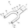
도 1을 참조하면, 웨이퍼 이송용 블레이드(100)는 몸체(102), 몸체(102)로부터 연장되는 제1 가지(104) 및 몸체(102)로부터 연장되는 제2 가지(106)를 포함하며, Y 자 형상을 갖는다.Referring to Figure 1, a
몸체(102), 제1 가지(104) 및 제2 가지(106)는 웨이퍼(도 3의 10 참조)에 정전기가 발생하지 않도록 방지하는 재질을 포함할 수 있다. 바람직하게는 몸체(102), 제1 가지(104) 및 제2 가지(106)는 전기절연저항이 상대적으로 낮은 금속 산화물을 포함할 수 있다. 예를 들면, 전기절연저항이 1옴에 가까운 이산화 타이타늄(titanium dioxide)을 포함할 수 있다. 또는, 몸체(102), 제1 가지(104) 및 제2 가지(106)의 표면이 이산화 타이타늄(titanium dioxide)으로 코팅될 수 있다. 또는, 몸체(102), 제1 가지(104) 및 제2 가지(106)는 알루미늄(aluminum)을 포함한 세라믹(ceramic) 재질을 포함할 수 있다.The
몸체(102), 제1 가지(104) 및 제2 가지(106)가 이산화 타이타늄(titanium dioxide)으로 만들어진 경우, IMP 공정 및 애슁(ashing) 공정을 거친 웨이퍼를 이송하는데 있어서, 종래 일반적인 웨이퍼 이송용 블레이드의 경우에 비해, 정전기량이 평균6kv/in 에서 0.1kv/in 로 줄어들었음을 실험에 의해 확인하였다.When the
웨이퍼 이송용 블레이드(100) 상에는 제1 내지 제3 진공홀들(110, 120, 130)이 배치된다. 제1 내지 제3 진공홀들(110, 120, 130)은 진공압을 발생시켜 상기 웨이퍼를 진공 흡착 시킨다. 제1 내지 제3 진공홀들(110, 120, 130)은 상기 웨이퍼를 이송하기 위해 적절한 위치에 배치될 수 있다. 예를 들면, 제1 진공홀(110)은 몸체(102) 상에 배치되고, 제2 진공홀(120)은 제1 가지(104) 상에 배치되고, 제3 진공홀(130)은 제2 가지(106) 상에 배치될 수 있다. 따라서, 상기 제1 내지 제3 진공홀들(110, 120, 130)은 삼각형으로 배치되어, 상기 삼각형의 중심이 상기 웨이퍼의 중심과 일치하도록 상기 웨이퍼를 웨이퍼 이송용 블레이드(100) 상에 위치시키고, 상기 진공압을 이용하여 상기 웨이퍼를 고정 시킨 후 이송할 수 있다. 이때, 상기 웨이퍼의 하면은 웨이퍼 이송용 블레이드(100)의 몸체(102), 제1 가지(104) 및 제2 가지(106)와 접촉하게 된다.First to third vacuum holes 110, 120, and 130 are disposed on the
제1 내지 제3 진공홀들(110, 120, 130)은 동일한 진공압을 발생하여, 상기 웨이퍼에 대해 동일한 힘을 가할 수 있다.The first to third vacuum holes 110, 120, and 130 generate the same vacuum pressure to apply the same force to the wafer.
도시하지는 않았으나, 상기 웨이퍼 이송용 블레이드(100)는 상기 몸체(102)와 전기적으로 연결되어 정전기를 제거할 수 있는 그라운드부를 더 포함할 수 있다.Although not shown, the
도 2 는 본 발명의 다른 실시예에 따른 웨이퍼 이송용 블레이드를 나타내는 사시도이다.2 is a perspective view showing a wafer transfer blade according to another embodiment of the present invention.
도 2를 참조하면, 웨이퍼 이송용 블레이드(200)는 가이드월(203), 제1 내지 제3 접촉 패드(212, 222, 232)를 더 포함하는 것을 제외하고, 도 1의 웨이퍼 이송용 블레이드(100)와 실질적으로 동일하다. 따라서 반복되는 설명은 생략하거나 간략히 한다.2, the
웨이퍼 이송용 블레이드(200)는 몸체(202), 몸체(202)로부터 연장되는 제1 가지(204) 및 몸체(202)로부터 연장되는 제2 가지(206)를 포함한다.The
웨이퍼 이송용 블레이드(200) 상에는 제1 내지 제3 접촉 패드들(212, 222, 232)이 배치된다. 제1 접촉 패드(212)는 몸체(202) 상에 배치되고, 제2 접촉 패드(222)는 제1 가지(204) 상에 배치되며, 제3 접촉 패드(232)는 제2 가지(206) 상에 배치된다. 제1 내지 제3 접촉 패드들(212, 222, 232)은 이송되는 웨이퍼(도 3의 10 참조)와 접촉하고, 소정의 두께를 가지므로, 몸체(202), 제1 가지(204) 및 제2 가지(206)가 상기 웨이퍼와 이격되도록 한다.First to
제1 내지 제3 접촉 패드들(212, 222, 232)은 상기 웨이퍼와 접촉하므로, 상기 웨이퍼 표면에 손상을 주지 않기 위해 탄성을 가진 재질로 이루어질 수 있다. 즉, 제1 내지 제3 접촉 패드들(212, 222, 232)은 폴리이미드계 플라스틱, 예를 들면, Dupont사의 Vespel로 이루어질 수 있다.The first to
몸체(202)에는 가이드월(203)이 형성된다. 가이드월(203)은 제1 내지 제3 접촉 패드들(212, 222, 232)의 두께보다 높은 높이를 가지므로, 웨이퍼 이송용 블레이드(200)에 안착되는 상기 웨이퍼가 정위치에서 벗어나는 것을 방지할 수 있다.A
도 3은 도 2의 상기 블레이드의 웨이퍼 로딩(loading)을 설명하기 위한 단면도이다.3 is a cross-sectional view for explaining wafer loading of the blade of FIG. 2;
도 2 및 3을 참조하면, 블레이드(200) 상에 웨이퍼(10)가 위치함에 따라, 제1 내지 제3 접촉 패드들(212, 222, 232)이 웨이퍼(10)와 접촉한다. 제1 내지 제3 접촉 패드들(212, 222, 232)은 소정의 두께를 가지므로, 몸체(202), 제1 가지(204) 및 제2 가지(206)가 웨이퍼(10)와 이격된다. 제1 내지 제3 접촉 패드들(212, 222, 232)에는 각각 제1 내지 제3 진공홀(210, 220, 230)이 형성되고, 몸체(202), 제1 가지(204) 및 제2 가지(206) 내에 형성되는 진공 통로(240)에 연결된다. 진공 통로(240)는 진공발생장치(미도시)에 연결되어, 필요에 따라 진공압을 발생하여, 웨이퍼(10)를 고정할 수 있다. 이때, 제1 내지 제3 접촉 패드들(212, 222, 232)은 탄성을 가진 재질로 이루어 지므로, 웨이퍼(10)에 손상을 가하지 않을 수 있다. 제1 내지 제3 접촉 패드들(212, 222, 232)은 폴리이미드계 플라스틱을 포함할 수 있고, 몸체(102), 제1 가지(104) 및 제2 가지(106)는 이산화 타이타늄(titanium dioxide)을 포함할 수 있으므로, 웨이퍼(10)에 정전기가 발생하는 것을 방지할 수 있다.Referring to FIGS. 2 and 3, as the
도 4는 본 발명의 다른 실시예에 따른 웨이퍼 이송용 블레이드를 나타내는 사시도이다.4 is a perspective view showing a wafer transfer blade according to another embodiment of the present invention.
도 4를 참조하면, 웨이퍼 이송용 블레이드(300)는 몸체(310), 제1 가이드월(320) 및 제2 가이드월(330)을 포함한다. 제1 가이드월(320) 및 제2 가이드월(330)은 몸체(310) 보다 높은 높이로 형성되어, 웨이퍼의 이탈을 방지한다.Referring to FIG. 4, the
상기 웨이퍼 이송시, 상기 웨이퍼는 몸체(310)상에 배치되어 몸체(310)와 접촉한다.Upon wafer transfer, the wafer is disposed on the
몸체(310)는 정전기가 발생하지 않도록 방지하는 재질을 포함할 수 있다. 바람직하게는 몸체(310)는 전기절연저항이 상대적으로 낮은 금속 산화물을 포함할 수 있다. 예를 들면, 이산화 타이타늄(titanium dioxide)을 포함할 수 있다. 또는, 몸체(310)의 표면이 이산화 타이타늄(titanium dioxide)으로 코팅될 수 있다. 또는, 몸체(310)는 알루미늄(aluminum)을 포함한 세라믹(ceramic) 재질을 포함할 수 있다.The
웨이퍼 이송용 블레이드(300)는 별도의 그립 부재가 없이 사용될 수 있으며, 또한, 몸체(310)상에 위치하는 상기 웨이퍼의 이탈을 방지하기 위해 별도의 그립 부재(미도시)를 더 포함할 수 있다.The
도 5는 본 발명의 다른 실시예에 따른 웨이퍼 이송용 블레이드를 나타내는 사시도이다.5 is a perspective view showing a wafer transfer blade according to another embodiment of the present invention.
도 5를 참조하면, 웨이퍼 이송용 블레이드(400)는 복수의 접촉 패드(440)를 더 포함하는 것을 제외하고, 도 4의 웨이퍼 이송용 블레이드(300)와 실질적으로 동일하다. 따라서 반복되는 설명은 생략하거나 간략히 한다.Referring to FIG. 5, the
접촉 패드들(440)은 몸체(410)상에 배치된다. 접촉 패드들(440)은 삼각형 형상으로 배치될 수 있다. 접촉 패드들(440)은 제1 가이드월(320) 및 제2 가이드월(330)의 높이보다 작은 소정의 두께를 가지며, 상기 웨이퍼가 몸체(310)로부터 이격되도록 한다.The
접촉 패드들(440)은 상기 웨이퍼와 접촉하므로, 상기 웨이퍼 표면에 손상을 주지 않기 위해 탄성을 가진 재질을 포함할 수 있다. 즉, 접촉 패드들(440)은 폴리이미드계 플라스틱, 예를 들면, Dupont사의 Vespel을 포함할 수 있다.The
도 6은 도 5의 상기 웨이퍼 이송용 블레이드의 웨이퍼를 로딩(loading)을 설명하기 위한 단면도이다.Fig. 6 is a sectional view for explaining loading of the wafer of the wafer transfer blade of Fig. 5;
도 5 및 6을 참조하면, 웨이퍼 이송용 블레이드(400) 상에 웨이퍼(10)가 위치함에 따라, 접촉 패드들(440)이 웨이퍼(10)와 접촉한다. 접촉 패드들(440)은 소정의 두께를 가지므로, 몸체(410)가 웨이퍼(10)와 이격된다. 웨이퍼 이송용 블레이드(400)는 제1 가이드월(320) 및 제2 가이드월(430)을 포함하므로, 웨이퍼(10)가 몸체(410)로부터 이탈되지 않고 고정될 수 있다. 이때, 접촉 패드들(440)은 탄성을 가진 재질을 포함할 수 있으므로, 웨이퍼(10)에 손상을 가하지 않을 수 있다. 접촉 패드들(440)은 폴리이미드계 플라스틱을 포함하고, 몸체(410)는 이산화 타이타늄(titanium dioxide)을 포함할 수 있으므로, 웨이퍼(10)에 정전기가 발생하는 것을 방지할 수 있다.Referring to FIGS. 5 and 6, as the
도 7은 본 발명의 다른 실시예에 따른 웨이퍼 이송 장치를 나타내는 사시도이다. 도 8a 및 8b는 도7의 웨이퍼 이송장치가 웨이퍼 수납용기에 웨이퍼를 언로딩하는 것을 설명하기 위한 개략적인 단면도이다.7 is a perspective view showing a wafer transfer apparatus according to another embodiment of the present invention. Figs. 8A and 8B are schematic cross-sectional views for explaining the wafer transfer device of Fig. 7 unloading a wafer into a wafer storage container. Fig.
도 7 내지 8b를 참조하면, 웨이퍼 이송장치(1000)는 웨이퍼 이송용 블레이드(200), 웨이퍼 이송용 블레이드(200)에 연결된 제1 암(1100) 및 제1 암(110)과 연결된 제2 암(1200)을 포함한다. 블레이드(200)는 도 2의 웨이퍼 이송용 블레이드와 실질적으로 동일하다. 제1 암(1100) 및 제2 암(1200)은 서로 상대적인 움직임이 가능하며, 이에 따라 웨이퍼 이송용 블레이드(200)를 상하 좌우로 이동시킬 수 있다.7 to 8B, the wafer transfer apparatus 1000 includes a
FOUP(front opening unified Pod 50)내에 위치한 웨이퍼(10)를 웨이퍼 이송장치(1000)를 이용하여 로딩(loading)하는 것이 도 8a에 설명된다. FOUP(50)은 내부에 웨이퍼(10)를 지지하기 위한 복수의 슬롯들(20)을 포함한다. 웨이퍼(10)는 슬롯(20)에 의해 지지되어, FOUP(50)의 내부에 수납된다. 웨이퍼 이송장치(1000)의 웨이퍼 이송용 블레이드(200)를 FOUP(50)에 수납된 웨이퍼(10) 하부에서부터 웨이퍼(10) 하부의 평면에 대해 수직한 방향으로 이동시켜 웨이퍼(10)를 로딩(loading)한다. 이때, 도 2에서 설명한 바와 같이 진공압을 이용하여 웨이퍼(10)를 고정시킬 수 있다.Loading of the
웨이퍼 이송용 블레이드(200)는 이산화 타이타늄(titanium dioxide)을 포함할 수 있고, 제1 내지 제3 접촉 패드들(212, 222, 도 2의 232 참조)은 폴리이미드계 플라스틱을 포함할 수 있으므로, 상기 과정에서 웨이퍼(10)에 정전기가 발생하는 것을 방지할 수 있다.The
웨이퍼(10)를 웨이퍼 이송장치(1000)를 이용하여 FOUP(50)내에 언로딩(un-loading)하는 것이 도 8a에 설명된다. 웨이퍼 이송장치(1000)의 웨이퍼 이송용 블레이드(200)를 이용하여 웨이퍼(10)를 슬롯(20) 상에 위치시킨다. 진공압을 소멸시키고, 웨이퍼 이송용 블레이드(200)를 웨이퍼 하부 표면으로부터 수직으로 이동시켜, 웨이퍼(10)를 FOUP(50) 내부에 언로딩(un-loading) 할 수 있다.The un-loading of the
웨이퍼 이송용 블레이드(200)는 이산화 타이타늄(titanium dioxide)을 포함할 수 있고, 제1 내지 제3 접촉 패드들(212, 222, 도 2의 232 참조)은 폴리이미드계 플라스틱을 포함할 수 있으므로, 상기 과정에서 웨이퍼(10)에 정전기가 발생하는 것을 방지할 수 있다. 따라서, 웨이퍼(10) 언로딩(un-loading)시 웨이퍼(10)가 정전기에 의해 웨이퍼 이송용 블레이드(200)에 들러붙어(sticking), 웨이퍼(10)가 슬롯(20)과 충격하는 것을 방지할 수 있다.The
본 발명의 실시예들에 따르면, 웨이퍼 이송용 블레이드는 전기절연저항이 상대적으로 낮은 금속 산화물을 포함하므로, IMP(implant) 공정 및 애슁(ashing) 공정을 거친 웨이퍼를 이송하는데 있어서, 정전기 발생을 효과적으로 방지할 수 있다.According to embodiments of the present invention, since the wafer transfer blade includes a metal oxide having a relatively low electrical insulation resistance, in transferring a wafer through an IMP (implant) process and an ashing process, .
또한, 상기 웨이퍼 이송용 블레이드는 몸체, 제1 가지 및 제2 가지 상에 각각 배치된 제1 내지 제3 진공홀을 포함하므로, 상기 웨이퍼에 대한 손상을 최소화 할 수 있다.In addition, since the wafer transfer blade includes the first through third vacuum holes disposed on the body, the first branch and the second branch, respectively, damage to the wafer can be minimized.
또한, 상기 웨이퍼 이송용 블레이드는 탄성 재질을 포함하는 제1 내지 제3 접촉 패드들을 포함하므로, 상기In addition, since the wafer transfer blade includes first to third contact pads including an elastic material,
또한, 상기 웨이퍼 이송용 블레이드를 포함하는 웨이퍼 이송 장치는 상기 웨이퍼 이송용 블레이드를 FOUP에 언로딩(un-loading) 시 상기 블레이드를 상기 웨이퍼와 수직인 방향으로 분리되므로, 상기 웨이퍼에 대한 손상을 최소화 할 수 있다.Further, the wafer transfer device including the wafer transfer blade separates the blade in a direction perpendicular to the wafer when unloading the wafer transfer blade to the FOUP, thereby minimizing damage to the wafer can do.
상술한 바와 같이 본 발명의 바람직한 실시예들을 참조하여 설명하였지만, 해당 기술 분야의 숙련된 당업자는 하기의 특허 청구의 범위에 기재된 본 발명의 사상 및 영역으로부터 벗어나지 않는 범위 내에서 본 발명을 다양하게 수정 및 변경시킬 수 있음을 이해할 수 있을 것이다It will be apparent to those skilled in the art that various modifications and variations can be made in the present invention without departing from the spirit and scope of the invention as defined in the appended claims. And can be changed
100, 200, 300, 400: 웨이퍼 이송용 블레이드
102: 몸체104: 제1 가지
106: 제2 가지110: 제1 진공홀
120: 제2 진공홀130: 제3 진공홀
212: 제1 접촉 패드222: 제2 접촉 패드
232: 제3 접촉 패드203: 가이드월100, 200, 300, 400: blade for wafer transfer
102: body 104: first branch
106: second branch 110: first vacuum hole
120: second vacuum hole 130: third vacuum hole
212: first contact pad 222: second contact pad
232: third contact pad 203: guide wall
Claims (10)
Translated fromKorean상기 몸체 상에 형성되고 진공압을 발생시켜 상기 웨이퍼를 흡착하는 진공홀을 구비하는 흡착부를 포함하고,
상기 몸체는 정전기 방지를 위한 금속 산화물을 포함하는 웨이퍼 이송용 블레이드.A body for supporting a wafer; And
And a vacuum hole formed on the body and generating vacuum pressure to attract the wafer,
Wherein the body comprises a metal oxide for preventing static electricity.
상기 진공홀은 상기 몸체 상에 형성된 제1 진공홀, 상기 제1 가지 상에 형성된 제2 진공홀 및 상기 제2 가지 상에 형성된 제3 진공홀을 포함하고,
상기 몸체, 상기 제1 가지 및 상기 제2 가지는 Y자 형상을 이루고, 상기 제1 내지 제3 진공홀들은 삼각형 형상으로 배치된 것을 특징으로 하는 웨이퍼 이송용 블레이드.3. The apparatus of claim 2, further comprising a first branch extending from the body and a second branch extending from the body,
Wherein the vacuum hole includes a first vacuum hole formed on the body, a second vacuum hole formed on the first branch, and a third vacuum hole formed on the second branch,
Wherein the body, the first branch, and the second branch are Y-shaped, and the first through third vacuum holes are arranged in a triangular shape.
상기 제1 내지 제3 진공홀들은 각각 상기 제1 내지 제3 접촉 패드들의 개구와 연통되고,
상기 웨이퍼가 이송될 때, 상기 웨이퍼는 상기 제1 내지 제3 접촉 패드들과 접촉하고, 상기 몸체, 상기 제1 가지 및 상기 제2 가지와 이격되는 것을 특징으로 하는 웨이퍼 이송용 블레이드.5. The device of claim 4, further comprising: a first contact pad disposed on the body and having an opening formed therein, a second contact pad disposed on the first branch and having an opening formed therein, a third contact disposed on the second branch, Further comprising a pad,
The first through third vacuum holes communicate with the openings of the first through third contact pads, respectively,
Wherein when the wafer is transferred, the wafer contacts the first through third contact pads, and is spaced apart from the body, the first branch, and the second branch.
상기 몸체의 상기 일측과 대향하는 타측에 형성된 제2 가이드월을 포함하고,
상기 몸체는 정전기 방지를 위한 금속 산화물을 포함하는 것을 특징으로 하는 웨이퍼 이송용 블레이드.A body for supporting a wafer; And
And a second guide wall formed on the other side opposite to the one side of the body,
Wherein the body comprises a metal oxide for preventing static electricity.
상기 웨이퍼 이송용 블레이드와 연결된 제1 암(arm)을 포함하는 웨이퍼 이송 장치.A body for supporting a wafer, and a suction part formed on the body and having a vacuum hole for generating vacuum pressure to suction the wafer, wherein the body comprises a metal oxide for preventing static electricity, ; And
And a first arm connected to the wafer transfer blade.
상기 제1 암에 연결되는 제2 암을 더 포함하고, 상기 제1 암과 상기 제2 암의 상호 움직임에 의해 상기 웨이퍼 이송용 블레이드가 웨이퍼의 하면과 수직하게 이동 가능한 것을 특징으로 하는 웨이퍼 이송장치.
10. The method of claim 9, wherein the body of the wafer transfer blade comprises titanium dioxide (TiO2)
Further comprising a second arm connected to the first arm, wherein the wafer transfer blade is vertically movable with respect to the lower surface of the wafer by mutual movement of the first arm and the second arm. .
Priority Applications (2)
| Application Number | Priority Date | Filing Date | Title |
|---|---|---|---|
| KR1020130015605AKR20140102782A (en) | 2013-02-14 | 2013-02-14 | Blade for transferring wafer and wafer transferring apparatus having the same |
| US14/178,392US20140227072A1 (en) | 2013-02-14 | 2014-02-12 | Wafer transfer blade and wafer transfer apparatus having the same |
Applications Claiming Priority (1)
| Application Number | Priority Date | Filing Date | Title |
|---|---|---|---|
| KR1020130015605AKR20140102782A (en) | 2013-02-14 | 2013-02-14 | Blade for transferring wafer and wafer transferring apparatus having the same |
Publications (1)
| Publication Number | Publication Date |
|---|---|
| KR20140102782Atrue KR20140102782A (en) | 2014-08-25 |
Family
ID=51297527
Family Applications (1)
| Application Number | Title | Priority Date | Filing Date |
|---|---|---|---|
| KR1020130015605AWithdrawnKR20140102782A (en) | 2013-02-14 | 2013-02-14 | Blade for transferring wafer and wafer transferring apparatus having the same |
Country Status (2)
| Country | Link |
|---|---|
| US (1) | US20140227072A1 (en) |
| KR (1) | KR20140102782A (en) |
Cited By (2)
| Publication number | Priority date | Publication date | Assignee | Title |
|---|---|---|---|---|
| WO2017135518A1 (en)* | 2016-02-05 | 2017-08-10 | 주식회사 이오테크닉스 | Wafer alignment apparatus and wafer transfer apparatus |
| KR20230166425A (en) | 2022-05-30 | 2023-12-07 | (주) 에이티엠 | Ceramic materials for transporting wafer and the manufacuring method of the same |
Families Citing this family (392)
| Publication number | Priority date | Publication date | Assignee | Title |
|---|---|---|---|---|
| JP5123851B2 (en)* | 2005-07-08 | 2013-01-23 | クロッシング オートメーション インコーポレイテッド | Work piece container for storing the work piece |
| US10378106B2 (en) | 2008-11-14 | 2019-08-13 | Asm Ip Holding B.V. | Method of forming insulation film by modified PEALD |
| US9394608B2 (en) | 2009-04-06 | 2016-07-19 | Asm America, Inc. | Semiconductor processing reactor and components thereof |
| US8802201B2 (en) | 2009-08-14 | 2014-08-12 | Asm America, Inc. | Systems and methods for thin-film deposition of metal oxides using excited nitrogen-oxygen species |
| US9312155B2 (en) | 2011-06-06 | 2016-04-12 | Asm Japan K.K. | High-throughput semiconductor-processing apparatus equipped with multiple dual-chamber modules |
| US9793148B2 (en) | 2011-06-22 | 2017-10-17 | Asm Japan K.K. | Method for positioning wafers in multiple wafer transport |
| US10364496B2 (en) | 2011-06-27 | 2019-07-30 | Asm Ip Holding B.V. | Dual section module having shared and unshared mass flow controllers |
| US10854498B2 (en) | 2011-07-15 | 2020-12-01 | Asm Ip Holding B.V. | Wafer-supporting device and method for producing same |
| US20130023129A1 (en) | 2011-07-20 | 2013-01-24 | Asm America, Inc. | Pressure transmitter for a semiconductor processing environment |
| US9017481B1 (en) | 2011-10-28 | 2015-04-28 | Asm America, Inc. | Process feed management for semiconductor substrate processing |
| US8946830B2 (en) | 2012-04-04 | 2015-02-03 | Asm Ip Holdings B.V. | Metal oxide protective layer for a semiconductor device |
| US9558931B2 (en) | 2012-07-27 | 2017-01-31 | Asm Ip Holding B.V. | System and method for gas-phase sulfur passivation of a semiconductor surface |
| US9659799B2 (en) | 2012-08-28 | 2017-05-23 | Asm Ip Holding B.V. | Systems and methods for dynamic semiconductor process scheduling |
| US9021985B2 (en) | 2012-09-12 | 2015-05-05 | Asm Ip Holdings B.V. | Process gas management for an inductively-coupled plasma deposition reactor |
| US9324811B2 (en) | 2012-09-26 | 2016-04-26 | Asm Ip Holding B.V. | Structures and devices including a tensile-stressed silicon arsenic layer and methods of forming same |
| US10714315B2 (en) | 2012-10-12 | 2020-07-14 | Asm Ip Holdings B.V. | Semiconductor reaction chamber showerhead |
| US9640416B2 (en) | 2012-12-26 | 2017-05-02 | Asm Ip Holding B.V. | Single-and dual-chamber module-attachable wafer-handling chamber |
| US20160376700A1 (en) | 2013-02-01 | 2016-12-29 | Asm Ip Holding B.V. | System for treatment of deposition reactor |
| US9589770B2 (en) | 2013-03-08 | 2017-03-07 | Asm Ip Holding B.V. | Method and systems for in-situ formation of intermediate reactive species |
| US9484191B2 (en) | 2013-03-08 | 2016-11-01 | Asm Ip Holding B.V. | Pulsed remote plasma method and system |
| US8993054B2 (en) | 2013-07-12 | 2015-03-31 | Asm Ip Holding B.V. | Method and system to reduce outgassing in a reaction chamber |
| US9018111B2 (en) | 2013-07-22 | 2015-04-28 | Asm Ip Holding B.V. | Semiconductor reaction chamber with plasma capabilities |
| US9793115B2 (en) | 2013-08-14 | 2017-10-17 | Asm Ip Holding B.V. | Structures and devices including germanium-tin films and methods of forming same |
| US9240412B2 (en) | 2013-09-27 | 2016-01-19 | Asm Ip Holding B.V. | Semiconductor structure and device and methods of forming same using selective epitaxial process |
| US9556516B2 (en) | 2013-10-09 | 2017-01-31 | ASM IP Holding B.V | Method for forming Ti-containing film by PEALD using TDMAT or TDEAT |
| US10179947B2 (en) | 2013-11-26 | 2019-01-15 | Asm Ip Holding B.V. | Method for forming conformal nitrided, oxidized, or carbonized dielectric film by atomic layer deposition |
| US10683571B2 (en) | 2014-02-25 | 2020-06-16 | Asm Ip Holding B.V. | Gas supply manifold and method of supplying gases to chamber using same |
| US10167557B2 (en) | 2014-03-18 | 2019-01-01 | Asm Ip Holding B.V. | Gas distribution system, reactor including the system, and methods of using the same |
| US9447498B2 (en) | 2014-03-18 | 2016-09-20 | Asm Ip Holding B.V. | Method for performing uniform processing in gas system-sharing multiple reaction chambers |
| US11015245B2 (en) | 2014-03-19 | 2021-05-25 | Asm Ip Holding B.V. | Gas-phase reactor and system having exhaust plenum and components thereof |
| US9343350B2 (en)* | 2014-04-03 | 2016-05-17 | Asm Ip Holding B.V. | Anti-slip end effector for transporting workpiece using van der waals force |
| US9404587B2 (en) | 2014-04-24 | 2016-08-02 | ASM IP Holding B.V | Lockout tagout for semiconductor vacuum valve |
| US10858737B2 (en) | 2014-07-28 | 2020-12-08 | Asm Ip Holding B.V. | Showerhead assembly and components thereof |
| US9543180B2 (en) | 2014-08-01 | 2017-01-10 | Asm Ip Holding B.V. | Apparatus and method for transporting wafers between wafer carrier and process tool under vacuum |
| US9890456B2 (en) | 2014-08-21 | 2018-02-13 | Asm Ip Holding B.V. | Method and system for in situ formation of gas-phase compounds |
| US9657845B2 (en) | 2014-10-07 | 2017-05-23 | Asm Ip Holding B.V. | Variable conductance gas distribution apparatus and method |
| US10941490B2 (en) | 2014-10-07 | 2021-03-09 | Asm Ip Holding B.V. | Multiple temperature range susceptor, assembly, reactor and system including the susceptor, and methods of using the same |
| KR102300403B1 (en) | 2014-11-19 | 2021-09-09 | 에이에스엠 아이피 홀딩 비.브이. | Method of depositing thin film |
| KR102263121B1 (en) | 2014-12-22 | 2021-06-09 | 에이에스엠 아이피 홀딩 비.브이. | Semiconductor device and manufacuring method thereof |
| US9478415B2 (en) | 2015-02-13 | 2016-10-25 | Asm Ip Holding B.V. | Method for forming film having low resistance and shallow junction depth |
| US10529542B2 (en) | 2015-03-11 | 2020-01-07 | Asm Ip Holdings B.V. | Cross-flow reactor and method |
| US10276355B2 (en) | 2015-03-12 | 2019-04-30 | Asm Ip Holding B.V. | Multi-zone reactor, system including the reactor, and method of using the same |
| US10458018B2 (en) | 2015-06-26 | 2019-10-29 | Asm Ip Holding B.V. | Structures including metal carbide material, devices including the structures, and methods of forming same |
| US10600673B2 (en) | 2015-07-07 | 2020-03-24 | Asm Ip Holding B.V. | Magnetic susceptor to baseplate seal |
| US9899291B2 (en) | 2015-07-13 | 2018-02-20 | Asm Ip Holding B.V. | Method for protecting layer by forming hydrocarbon-based extremely thin film |
| US10043661B2 (en) | 2015-07-13 | 2018-08-07 | Asm Ip Holding B.V. | Method for protecting layer by forming hydrocarbon-based extremely thin film |
| US10083836B2 (en) | 2015-07-24 | 2018-09-25 | Asm Ip Holding B.V. | Formation of boron-doped titanium metal films with high work function |
| US10087525B2 (en) | 2015-08-04 | 2018-10-02 | Asm Ip Holding B.V. | Variable gap hard stop design |
| US20170040205A1 (en)* | 2015-08-05 | 2017-02-09 | Lam Research Corporation | High-hardness-material-powder infused elastomer for high friction and compliance for silicon wafer transfer |
| US9647114B2 (en) | 2015-08-14 | 2017-05-09 | Asm Ip Holding B.V. | Methods of forming highly p-type doped germanium tin films and structures and devices including the films |
| US9711345B2 (en) | 2015-08-25 | 2017-07-18 | Asm Ip Holding B.V. | Method for forming aluminum nitride-based film by PEALD |
| US9960072B2 (en) | 2015-09-29 | 2018-05-01 | Asm Ip Holding B.V. | Variable adjustment for precise matching of multiple chamber cavity housings |
| US9909214B2 (en) | 2015-10-15 | 2018-03-06 | Asm Ip Holding B.V. | Method for depositing dielectric film in trenches by PEALD |
| US10211308B2 (en) | 2015-10-21 | 2019-02-19 | Asm Ip Holding B.V. | NbMC layers |
| US10322384B2 (en) | 2015-11-09 | 2019-06-18 | Asm Ip Holding B.V. | Counter flow mixer for process chamber |
| US9455138B1 (en) | 2015-11-10 | 2016-09-27 | Asm Ip Holding B.V. | Method for forming dielectric film in trenches by PEALD using H-containing gas |
| WO2017084079A1 (en)* | 2015-11-20 | 2017-05-26 | Acm Research (Shanghai) Inc. | Robot arm for transporting semiconductor substrates |
| US9905420B2 (en) | 2015-12-01 | 2018-02-27 | Asm Ip Holding B.V. | Methods of forming silicon germanium tin films and structures and devices including the films |
| US9607837B1 (en) | 2015-12-21 | 2017-03-28 | Asm Ip Holding B.V. | Method for forming silicon oxide cap layer for solid state diffusion process |
| US9735024B2 (en) | 2015-12-28 | 2017-08-15 | Asm Ip Holding B.V. | Method of atomic layer etching using functional group-containing fluorocarbon |
| US9627221B1 (en) | 2015-12-28 | 2017-04-18 | Asm Ip Holding B.V. | Continuous process incorporating atomic layer etching |
| US11139308B2 (en) | 2015-12-29 | 2021-10-05 | Asm Ip Holding B.V. | Atomic layer deposition of III-V compounds to form V-NAND devices |
| US10529554B2 (en) | 2016-02-19 | 2020-01-07 | Asm Ip Holding B.V. | Method for forming silicon nitride film selectively on sidewalls or flat surfaces of trenches |
| US9754779B1 (en) | 2016-02-19 | 2017-09-05 | Asm Ip Holding B.V. | Method for forming silicon nitride film selectively on sidewalls or flat surfaces of trenches |
| US10468251B2 (en) | 2016-02-19 | 2019-11-05 | Asm Ip Holding B.V. | Method for forming spacers using silicon nitride film for spacer-defined multiple patterning |
| US10501866B2 (en) | 2016-03-09 | 2019-12-10 | Asm Ip Holding B.V. | Gas distribution apparatus for improved film uniformity in an epitaxial system |
| US10343920B2 (en) | 2016-03-18 | 2019-07-09 | Asm Ip Holding B.V. | Aligned carbon nanotubes |
| US9892913B2 (en) | 2016-03-24 | 2018-02-13 | Asm Ip Holding B.V. | Radial and thickness control via biased multi-port injection settings |
| US10190213B2 (en) | 2016-04-21 | 2019-01-29 | Asm Ip Holding B.V. | Deposition of metal borides |
| US10865475B2 (en) | 2016-04-21 | 2020-12-15 | Asm Ip Holding B.V. | Deposition of metal borides and silicides |
| US10087522B2 (en) | 2016-04-21 | 2018-10-02 | Asm Ip Holding B.V. | Deposition of metal borides |
| US10367080B2 (en) | 2016-05-02 | 2019-07-30 | Asm Ip Holding B.V. | Method of forming a germanium oxynitride film |
| US10032628B2 (en) | 2016-05-02 | 2018-07-24 | Asm Ip Holding B.V. | Source/drain performance through conformal solid state doping |
| KR102592471B1 (en) | 2016-05-17 | 2023-10-20 | 에이에스엠 아이피 홀딩 비.브이. | Method of forming metal interconnection and method of fabricating semiconductor device using the same |
| US11453943B2 (en) | 2016-05-25 | 2022-09-27 | Asm Ip Holding B.V. | Method for forming carbon-containing silicon/metal oxide or nitride film by ALD using silicon precursor and hydrocarbon precursor |
| US10388509B2 (en) | 2016-06-28 | 2019-08-20 | Asm Ip Holding B.V. | Formation of epitaxial layers via dislocation filtering |
| US9859151B1 (en) | 2016-07-08 | 2018-01-02 | Asm Ip Holding B.V. | Selective film deposition method to form air gaps |
| US10612137B2 (en) | 2016-07-08 | 2020-04-07 | Asm Ip Holdings B.V. | Organic reactants for atomic layer deposition |
| US9793135B1 (en) | 2016-07-14 | 2017-10-17 | ASM IP Holding B.V | Method of cyclic dry etching using etchant film |
| US10714385B2 (en) | 2016-07-19 | 2020-07-14 | Asm Ip Holding B.V. | Selective deposition of tungsten |
| KR102354490B1 (en) | 2016-07-27 | 2022-01-21 | 에이에스엠 아이피 홀딩 비.브이. | Method of processing a substrate |
| US9812320B1 (en) | 2016-07-28 | 2017-11-07 | Asm Ip Holding B.V. | Method and apparatus for filling a gap |
| US10177025B2 (en) | 2016-07-28 | 2019-01-08 | Asm Ip Holding B.V. | Method and apparatus for filling a gap |
| KR102532607B1 (en) | 2016-07-28 | 2023-05-15 | 에이에스엠 아이피 홀딩 비.브이. | Substrate processing apparatus and method of operating the same |
| US10395919B2 (en) | 2016-07-28 | 2019-08-27 | Asm Ip Holding B.V. | Method and apparatus for filling a gap |
| US9887082B1 (en) | 2016-07-28 | 2018-02-06 | Asm Ip Holding B.V. | Method and apparatus for filling a gap |
| KR101856608B1 (en)* | 2016-07-29 | 2018-05-15 | 세메스 주식회사 | Apparatus for treating substrate |
| US10090316B2 (en) | 2016-09-01 | 2018-10-02 | Asm Ip Holding B.V. | 3D stacked multilayer semiconductor memory using doped select transistor channel |
| US10410943B2 (en) | 2016-10-13 | 2019-09-10 | Asm Ip Holding B.V. | Method for passivating a surface of a semiconductor and related systems |
| US10643826B2 (en) | 2016-10-26 | 2020-05-05 | Asm Ip Holdings B.V. | Methods for thermally calibrating reaction chambers |
| US11532757B2 (en) | 2016-10-27 | 2022-12-20 | Asm Ip Holding B.V. | Deposition of charge trapping layers |
| US10435790B2 (en) | 2016-11-01 | 2019-10-08 | Asm Ip Holding B.V. | Method of subatmospheric plasma-enhanced ALD using capacitively coupled electrodes with narrow gap |
| US10643904B2 (en) | 2016-11-01 | 2020-05-05 | Asm Ip Holdings B.V. | Methods for forming a semiconductor device and related semiconductor device structures |
| US10229833B2 (en) | 2016-11-01 | 2019-03-12 | Asm Ip Holding B.V. | Methods for forming a transition metal nitride film on a substrate by atomic layer deposition and related semiconductor device structures |
| US10714350B2 (en) | 2016-11-01 | 2020-07-14 | ASM IP Holdings, B.V. | Methods for forming a transition metal niobium nitride film on a substrate by atomic layer deposition and related semiconductor device structures |
| US10134757B2 (en) | 2016-11-07 | 2018-11-20 | Asm Ip Holding B.V. | Method of processing a substrate and a device manufactured by using the method |
| KR102546317B1 (en) | 2016-11-15 | 2023-06-21 | 에이에스엠 아이피 홀딩 비.브이. | Gas supply unit and substrate processing apparatus including the same |
| US10340135B2 (en) | 2016-11-28 | 2019-07-02 | Asm Ip Holding B.V. | Method of topologically restricted plasma-enhanced cyclic deposition of silicon or metal nitride |
| KR102762543B1 (en) | 2016-12-14 | 2025-02-05 | 에이에스엠 아이피 홀딩 비.브이. | Substrate processing apparatus |
| US11581186B2 (en) | 2016-12-15 | 2023-02-14 | Asm Ip Holding B.V. | Sequential infiltration synthesis apparatus |
| US11447861B2 (en) | 2016-12-15 | 2022-09-20 | Asm Ip Holding B.V. | Sequential infiltration synthesis apparatus and a method of forming a patterned structure |
| US9916980B1 (en) | 2016-12-15 | 2018-03-13 | Asm Ip Holding B.V. | Method of forming a structure on a substrate |
| KR102700194B1 (en) | 2016-12-19 | 2024-08-28 | 에이에스엠 아이피 홀딩 비.브이. | Substrate processing apparatus |
| US10269558B2 (en) | 2016-12-22 | 2019-04-23 | Asm Ip Holding B.V. | Method of forming a structure on a substrate |
| US10867788B2 (en) | 2016-12-28 | 2020-12-15 | Asm Ip Holding B.V. | Method of forming a structure on a substrate |
| US11390950B2 (en) | 2017-01-10 | 2022-07-19 | Asm Ip Holding B.V. | Reactor system and method to reduce residue buildup during a film deposition process |
| US10655221B2 (en) | 2017-02-09 | 2020-05-19 | Asm Ip Holding B.V. | Method for depositing oxide film by thermal ALD and PEALD |
| US10468261B2 (en) | 2017-02-15 | 2019-11-05 | Asm Ip Holding B.V. | Methods for forming a metallic film on a substrate by cyclical deposition and related semiconductor device structures |
| US10283353B2 (en) | 2017-03-29 | 2019-05-07 | Asm Ip Holding B.V. | Method of reforming insulating film deposited on substrate with recess pattern |
| US10529563B2 (en) | 2017-03-29 | 2020-01-07 | Asm Ip Holdings B.V. | Method for forming doped metal oxide films on a substrate by cyclical deposition and related semiconductor device structures |
| US10103040B1 (en) | 2017-03-31 | 2018-10-16 | Asm Ip Holding B.V. | Apparatus and method for manufacturing a semiconductor device |
| USD830981S1 (en) | 2017-04-07 | 2018-10-16 | Asm Ip Holding B.V. | Susceptor for semiconductor substrate processing apparatus |
| KR102457289B1 (en) | 2017-04-25 | 2022-10-21 | 에이에스엠 아이피 홀딩 비.브이. | Method for depositing a thin film and manufacturing a semiconductor device |
| US10770286B2 (en) | 2017-05-08 | 2020-09-08 | Asm Ip Holdings B.V. | Methods for selectively forming a silicon nitride film on a substrate and related semiconductor device structures |
| US10892156B2 (en) | 2017-05-08 | 2021-01-12 | Asm Ip Holding B.V. | Methods for forming a silicon nitride film on a substrate and related semiconductor device structures |
| US10446393B2 (en) | 2017-05-08 | 2019-10-15 | Asm Ip Holding B.V. | Methods for forming silicon-containing epitaxial layers and related semiconductor device structures |
| US10504742B2 (en) | 2017-05-31 | 2019-12-10 | Asm Ip Holding B.V. | Method of atomic layer etching using hydrogen plasma |
| US10886123B2 (en) | 2017-06-02 | 2021-01-05 | Asm Ip Holding B.V. | Methods for forming low temperature semiconductor layers and related semiconductor device structures |
| US12040200B2 (en) | 2017-06-20 | 2024-07-16 | Asm Ip Holding B.V. | Semiconductor processing apparatus and methods for calibrating a semiconductor processing apparatus |
| US11306395B2 (en) | 2017-06-28 | 2022-04-19 | Asm Ip Holding B.V. | Methods for depositing a transition metal nitride film on a substrate by atomic layer deposition and related deposition apparatus |
| US10685834B2 (en) | 2017-07-05 | 2020-06-16 | Asm Ip Holdings B.V. | Methods for forming a silicon germanium tin layer and related semiconductor device structures |
| KR20190009245A (en) | 2017-07-18 | 2019-01-28 | 에이에스엠 아이피 홀딩 비.브이. | Methods for forming a semiconductor device structure and related semiconductor device structures |
| US11374112B2 (en) | 2017-07-19 | 2022-06-28 | Asm Ip Holding B.V. | Method for depositing a group IV semiconductor and related semiconductor device structures |
| US11018002B2 (en) | 2017-07-19 | 2021-05-25 | Asm Ip Holding B.V. | Method for selectively depositing a Group IV semiconductor and related semiconductor device structures |
| US10541333B2 (en) | 2017-07-19 | 2020-01-21 | Asm Ip Holding B.V. | Method for depositing a group IV semiconductor and related semiconductor device structures |
| US10605530B2 (en) | 2017-07-26 | 2020-03-31 | Asm Ip Holding B.V. | Assembly of a liner and a flange for a vertical furnace as well as the liner and the vertical furnace |
| US10590535B2 (en) | 2017-07-26 | 2020-03-17 | Asm Ip Holdings B.V. | Chemical treatment, deposition and/or infiltration apparatus and method for using the same |
| US10312055B2 (en) | 2017-07-26 | 2019-06-04 | Asm Ip Holding B.V. | Method of depositing film by PEALD using negative bias |
| TWI815813B (en) | 2017-08-04 | 2023-09-21 | 荷蘭商Asm智慧財產控股公司 | Showerhead assembly for distributing a gas within a reaction chamber |
| US10770336B2 (en) | 2017-08-08 | 2020-09-08 | Asm Ip Holding B.V. | Substrate lift mechanism and reactor including same |
| US10692741B2 (en) | 2017-08-08 | 2020-06-23 | Asm Ip Holdings B.V. | Radiation shield |
| US11769682B2 (en) | 2017-08-09 | 2023-09-26 | Asm Ip Holding B.V. | Storage apparatus for storing cassettes for substrates and processing apparatus equipped therewith |
| US11139191B2 (en) | 2017-08-09 | 2021-10-05 | Asm Ip Holding B.V. | Storage apparatus for storing cassettes for substrates and processing apparatus equipped therewith |
| US10249524B2 (en) | 2017-08-09 | 2019-04-02 | Asm Ip Holding B.V. | Cassette holder assembly for a substrate cassette and holding member for use in such assembly |
| US10236177B1 (en) | 2017-08-22 | 2019-03-19 | ASM IP Holding B.V.. | Methods for depositing a doped germanium tin semiconductor and related semiconductor device structures |
| USD900036S1 (en) | 2017-08-24 | 2020-10-27 | Asm Ip Holding B.V. | Heater electrical connector and adapter |
| US11830730B2 (en) | 2017-08-29 | 2023-11-28 | Asm Ip Holding B.V. | Layer forming method and apparatus |
| US11056344B2 (en) | 2017-08-30 | 2021-07-06 | Asm Ip Holding B.V. | Layer forming method |
| KR102491945B1 (en) | 2017-08-30 | 2023-01-26 | 에이에스엠 아이피 홀딩 비.브이. | Substrate processing apparatus |
| US11295980B2 (en) | 2017-08-30 | 2022-04-05 | Asm Ip Holding B.V. | Methods for depositing a molybdenum metal film over a dielectric surface of a substrate by a cyclical deposition process and related semiconductor device structures |
| KR102401446B1 (en) | 2017-08-31 | 2022-05-24 | 에이에스엠 아이피 홀딩 비.브이. | Substrate processing apparatus |
| US10607895B2 (en) | 2017-09-18 | 2020-03-31 | Asm Ip Holdings B.V. | Method for forming a semiconductor device structure comprising a gate fill metal |
| KR102630301B1 (en) | 2017-09-21 | 2024-01-29 | 에이에스엠 아이피 홀딩 비.브이. | Method of sequential infiltration synthesis treatment of infiltrateable material and structures and devices formed using same |
| US10844484B2 (en) | 2017-09-22 | 2020-11-24 | Asm Ip Holding B.V. | Apparatus for dispensing a vapor phase reactant to a reaction chamber and related methods |
| US10658205B2 (en) | 2017-09-28 | 2020-05-19 | Asm Ip Holdings B.V. | Chemical dispensing apparatus and methods for dispensing a chemical to a reaction chamber |
| US10403504B2 (en) | 2017-10-05 | 2019-09-03 | Asm Ip Holding B.V. | Method for selectively depositing a metallic film on a substrate |
| US10319588B2 (en) | 2017-10-10 | 2019-06-11 | Asm Ip Holding B.V. | Method for depositing a metal chalcogenide on a substrate by cyclical deposition |
| US10923344B2 (en) | 2017-10-30 | 2021-02-16 | Asm Ip Holding B.V. | Methods for forming a semiconductor structure and related semiconductor structures |
| KR102443047B1 (en) | 2017-11-16 | 2022-09-14 | 에이에스엠 아이피 홀딩 비.브이. | Method of processing a substrate and a device manufactured by the same |
| US10910262B2 (en) | 2017-11-16 | 2021-02-02 | Asm Ip Holding B.V. | Method of selectively depositing a capping layer structure on a semiconductor device structure |
| US11022879B2 (en) | 2017-11-24 | 2021-06-01 | Asm Ip Holding B.V. | Method of forming an enhanced unexposed photoresist layer |
| WO2019103613A1 (en) | 2017-11-27 | 2019-05-31 | Asm Ip Holding B.V. | A storage device for storing wafer cassettes for use with a batch furnace |
| CN111344522B (en) | 2017-11-27 | 2022-04-12 | 阿斯莫Ip控股公司 | Including clean mini-environment device |
| US10290508B1 (en) | 2017-12-05 | 2019-05-14 | Asm Ip Holding B.V. | Method for forming vertical spacers for spacer-defined patterning |
| US10872771B2 (en) | 2018-01-16 | 2020-12-22 | Asm Ip Holding B. V. | Method for depositing a material film on a substrate within a reaction chamber by a cyclical deposition process and related device structures |
| KR102695659B1 (en) | 2018-01-19 | 2024-08-14 | 에이에스엠 아이피 홀딩 비.브이. | Method for depositing a gap filling layer by plasma assisted deposition |
| TWI799494B (en) | 2018-01-19 | 2023-04-21 | 荷蘭商Asm 智慧財產控股公司 | Deposition method |
| USD903477S1 (en) | 2018-01-24 | 2020-12-01 | Asm Ip Holdings B.V. | Metal clamp |
| US11018047B2 (en) | 2018-01-25 | 2021-05-25 | Asm Ip Holding B.V. | Hybrid lift pin |
| US10535516B2 (en) | 2018-02-01 | 2020-01-14 | Asm Ip Holdings B.V. | Method for depositing a semiconductor structure on a surface of a substrate and related semiconductor structures |
| USD880437S1 (en) | 2018-02-01 | 2020-04-07 | Asm Ip Holding B.V. | Gas supply plate for semiconductor manufacturing apparatus |
| US11081345B2 (en) | 2018-02-06 | 2021-08-03 | Asm Ip Holding B.V. | Method of post-deposition treatment for silicon oxide film |
| US10896820B2 (en) | 2018-02-14 | 2021-01-19 | Asm Ip Holding B.V. | Method for depositing a ruthenium-containing film on a substrate by a cyclical deposition process |
| WO2019158960A1 (en) | 2018-02-14 | 2019-08-22 | Asm Ip Holding B.V. | A method for depositing a ruthenium-containing film on a substrate by a cyclical deposition process |
| US10731249B2 (en) | 2018-02-15 | 2020-08-04 | Asm Ip Holding B.V. | Method of forming a transition metal containing film on a substrate by a cyclical deposition process, a method for supplying a transition metal halide compound to a reaction chamber, and related vapor deposition apparatus |
| US10658181B2 (en) | 2018-02-20 | 2020-05-19 | Asm Ip Holding B.V. | Method of spacer-defined direct patterning in semiconductor fabrication |
| KR102636427B1 (en) | 2018-02-20 | 2024-02-13 | 에이에스엠 아이피 홀딩 비.브이. | Substrate processing method and apparatus |
| US10975470B2 (en) | 2018-02-23 | 2021-04-13 | Asm Ip Holding B.V. | Apparatus for detecting or monitoring for a chemical precursor in a high temperature environment |
| US11473195B2 (en) | 2018-03-01 | 2022-10-18 | Asm Ip Holding B.V. | Semiconductor processing apparatus and a method for processing a substrate |
| US11629406B2 (en) | 2018-03-09 | 2023-04-18 | Asm Ip Holding B.V. | Semiconductor processing apparatus comprising one or more pyrometers for measuring a temperature of a substrate during transfer of the substrate |
| US11114283B2 (en) | 2018-03-16 | 2021-09-07 | Asm Ip Holding B.V. | Reactor, system including the reactor, and methods of manufacturing and using same |
| KR102646467B1 (en) | 2018-03-27 | 2024-03-11 | 에이에스엠 아이피 홀딩 비.브이. | Method of forming an electrode on a substrate and a semiconductor device structure including an electrode |
| US11088002B2 (en) | 2018-03-29 | 2021-08-10 | Asm Ip Holding B.V. | Substrate rack and a substrate processing system and method |
| US10510536B2 (en) | 2018-03-29 | 2019-12-17 | Asm Ip Holding B.V. | Method of depositing a co-doped polysilicon film on a surface of a substrate within a reaction chamber |
| US11230766B2 (en) | 2018-03-29 | 2022-01-25 | Asm Ip Holding B.V. | Substrate processing apparatus and method |
| KR102501472B1 (en) | 2018-03-30 | 2023-02-20 | 에이에스엠 아이피 홀딩 비.브이. | Substrate processing method |
| KR102600229B1 (en) | 2018-04-09 | 2023-11-10 | 에이에스엠 아이피 홀딩 비.브이. | Substrate supporting device, substrate processing apparatus including the same and substrate processing method |
| TWI811348B (en) | 2018-05-08 | 2023-08-11 | 荷蘭商Asm 智慧財產控股公司 | Methods for depositing an oxide film on a substrate by a cyclical deposition process and related device structures |
| US12025484B2 (en) | 2018-05-08 | 2024-07-02 | Asm Ip Holding B.V. | Thin film forming method |
| US12272527B2 (en) | 2018-05-09 | 2025-04-08 | Asm Ip Holding B.V. | Apparatus for use with hydrogen radicals and method of using same |
| KR20190129718A (en) | 2018-05-11 | 2019-11-20 | 에이에스엠 아이피 홀딩 비.브이. | Methods for forming a doped metal carbide film on a substrate and related semiconductor device structures |
| KR102596988B1 (en) | 2018-05-28 | 2023-10-31 | 에이에스엠 아이피 홀딩 비.브이. | Method of processing a substrate and a device manufactured by the same |
| US11718913B2 (en) | 2018-06-04 | 2023-08-08 | Asm Ip Holding B.V. | Gas distribution system and reactor system including same |
| TWI840362B (en) | 2018-06-04 | 2024-05-01 | 荷蘭商Asm Ip私人控股有限公司 | Wafer handling chamber with moisture reduction |
| US11286562B2 (en) | 2018-06-08 | 2022-03-29 | Asm Ip Holding B.V. | Gas-phase chemical reactor and method of using same |
| KR102568797B1 (en) | 2018-06-21 | 2023-08-21 | 에이에스엠 아이피 홀딩 비.브이. | Substrate processing system |
| US10797133B2 (en) | 2018-06-21 | 2020-10-06 | Asm Ip Holding B.V. | Method for depositing a phosphorus doped silicon arsenide film and related semiconductor device structures |
| KR102854019B1 (en) | 2018-06-27 | 2025-09-02 | 에이에스엠 아이피 홀딩 비.브이. | Periodic deposition method for forming a metal-containing material and films and structures comprising the metal-containing material |
| TWI873894B (en) | 2018-06-27 | 2025-02-21 | 荷蘭商Asm Ip私人控股有限公司 | Cyclic deposition methods for forming metal-containing material and films and structures including the metal-containing material |
| US10612136B2 (en) | 2018-06-29 | 2020-04-07 | ASM IP Holding, B.V. | Temperature-controlled flange and reactor system including same |
| KR102686758B1 (en) | 2018-06-29 | 2024-07-18 | 에이에스엠 아이피 홀딩 비.브이. | Method for depositing a thin film and manufacturing a semiconductor device |
| US10755922B2 (en) | 2018-07-03 | 2020-08-25 | Asm Ip Holding B.V. | Method for depositing silicon-free carbon-containing film as gap-fill layer by pulse plasma-assisted deposition |
| US10388513B1 (en) | 2018-07-03 | 2019-08-20 | Asm Ip Holding B.V. | Method for depositing silicon-free carbon-containing film as gap-fill layer by pulse plasma-assisted deposition |
| US10767789B2 (en) | 2018-07-16 | 2020-09-08 | Asm Ip Holding B.V. | Diaphragm valves, valve components, and methods for forming valve components |
| US10483099B1 (en) | 2018-07-26 | 2019-11-19 | Asm Ip Holding B.V. | Method for forming thermally stable organosilicon polymer film |
| US11053591B2 (en) | 2018-08-06 | 2021-07-06 | Asm Ip Holding B.V. | Multi-port gas injection system and reactor system including same |
| US10883175B2 (en) | 2018-08-09 | 2021-01-05 | Asm Ip Holding B.V. | Vertical furnace for processing substrates and a liner for use therein |
| US10829852B2 (en) | 2018-08-16 | 2020-11-10 | Asm Ip Holding B.V. | Gas distribution device for a wafer processing apparatus |
| US11430674B2 (en) | 2018-08-22 | 2022-08-30 | Asm Ip Holding B.V. | Sensor array, apparatus for dispensing a vapor phase reactant to a reaction chamber and related methods |
| KR102707956B1 (en) | 2018-09-11 | 2024-09-19 | 에이에스엠 아이피 홀딩 비.브이. | Method for deposition of a thin film |
| US11024523B2 (en) | 2018-09-11 | 2021-06-01 | Asm Ip Holding B.V. | Substrate processing apparatus and method |
| US11049751B2 (en) | 2018-09-14 | 2021-06-29 | Asm Ip Holding B.V. | Cassette supply system to store and handle cassettes and processing apparatus equipped therewith |
| CN110970344B (en) | 2018-10-01 | 2024-10-25 | Asmip控股有限公司 | Substrate holding apparatus, system comprising the same and method of using the same |
| US11232963B2 (en) | 2018-10-03 | 2022-01-25 | Asm Ip Holding B.V. | Substrate processing apparatus and method |
| KR102592699B1 (en) | 2018-10-08 | 2023-10-23 | 에이에스엠 아이피 홀딩 비.브이. | Substrate support unit and apparatuses for depositing thin film and processing the substrate including the same |
| US10847365B2 (en) | 2018-10-11 | 2020-11-24 | Asm Ip Holding B.V. | Method of forming conformal silicon carbide film by cyclic CVD |
| US10811256B2 (en) | 2018-10-16 | 2020-10-20 | Asm Ip Holding B.V. | Method for etching a carbon-containing feature |
| KR102546322B1 (en) | 2018-10-19 | 2023-06-21 | 에이에스엠 아이피 홀딩 비.브이. | Substrate processing apparatus and substrate processing method |
| KR102605121B1 (en) | 2018-10-19 | 2023-11-23 | 에이에스엠 아이피 홀딩 비.브이. | Substrate processing apparatus and substrate processing method |
| USD948463S1 (en) | 2018-10-24 | 2022-04-12 | Asm Ip Holding B.V. | Susceptor for semiconductor substrate supporting apparatus |
| US10381219B1 (en) | 2018-10-25 | 2019-08-13 | Asm Ip Holding B.V. | Methods for forming a silicon nitride film |
| US12378665B2 (en) | 2018-10-26 | 2025-08-05 | Asm Ip Holding B.V. | High temperature coatings for a preclean and etch apparatus and related methods |
| US11087997B2 (en) | 2018-10-31 | 2021-08-10 | Asm Ip Holding B.V. | Substrate processing apparatus for processing substrates |
| KR102748291B1 (en) | 2018-11-02 | 2024-12-31 | 에이에스엠 아이피 홀딩 비.브이. | Substrate support unit and substrate processing apparatus including the same |
| US11572620B2 (en) | 2018-11-06 | 2023-02-07 | Asm Ip Holding B.V. | Methods for selectively depositing an amorphous silicon film on a substrate |
| US11031242B2 (en) | 2018-11-07 | 2021-06-08 | Asm Ip Holding B.V. | Methods for depositing a boron doped silicon germanium film |
| US10847366B2 (en) | 2018-11-16 | 2020-11-24 | Asm Ip Holding B.V. | Methods for depositing a transition metal chalcogenide film on a substrate by a cyclical deposition process |
| US10818758B2 (en) | 2018-11-16 | 2020-10-27 | Asm Ip Holding B.V. | Methods for forming a metal silicate film on a substrate in a reaction chamber and related semiconductor device structures |
| US10559458B1 (en) | 2018-11-26 | 2020-02-11 | Asm Ip Holding B.V. | Method of forming oxynitride film |
| US12040199B2 (en) | 2018-11-28 | 2024-07-16 | Asm Ip Holding B.V. | Substrate processing apparatus for processing substrates |
| US11217444B2 (en) | 2018-11-30 | 2022-01-04 | Asm Ip Holding B.V. | Method for forming an ultraviolet radiation responsive metal oxide-containing film |
| KR102636428B1 (en) | 2018-12-04 | 2024-02-13 | 에이에스엠 아이피 홀딩 비.브이. | A method for cleaning a substrate processing apparatus |
| US11158513B2 (en) | 2018-12-13 | 2021-10-26 | Asm Ip Holding B.V. | Methods for forming a rhenium-containing film on a substrate by a cyclical deposition process and related semiconductor device structures |
| TWI874340B (en) | 2018-12-14 | 2025-03-01 | 荷蘭商Asm Ip私人控股有限公司 | Method of forming device structure, structure formed by the method and system for performing the method |
| TWI866480B (en) | 2019-01-17 | 2024-12-11 | 荷蘭商Asm Ip 私人控股有限公司 | Methods of forming a transition metal containing film on a substrate by a cyclical deposition process |
| KR102727227B1 (en) | 2019-01-22 | 2024-11-07 | 에이에스엠 아이피 홀딩 비.브이. | Semiconductor processing device |
| CN111524788B (en) | 2019-02-01 | 2023-11-24 | Asm Ip私人控股有限公司 | Method for forming topologically selective films of silicon oxide |
| TWI838458B (en) | 2019-02-20 | 2024-04-11 | 荷蘭商Asm Ip私人控股有限公司 | Apparatus and methods for plug fill deposition in 3-d nand applications |
| TWI873122B (en) | 2019-02-20 | 2025-02-21 | 荷蘭商Asm Ip私人控股有限公司 | Method of filling a recess formed within a surface of a substrate, semiconductor structure formed according to the method, and semiconductor processing apparatus |
| KR102626263B1 (en) | 2019-02-20 | 2024-01-16 | 에이에스엠 아이피 홀딩 비.브이. | Cyclical deposition method including treatment step and apparatus for same |
| TWI845607B (en) | 2019-02-20 | 2024-06-21 | 荷蘭商Asm Ip私人控股有限公司 | Cyclical deposition method and apparatus for filling a recess formed within a substrate surface |
| TWI842826B (en) | 2019-02-22 | 2024-05-21 | 荷蘭商Asm Ip私人控股有限公司 | Substrate processing apparatus and method for processing substrate |
| KR102858005B1 (en) | 2019-03-08 | 2025-09-09 | 에이에스엠 아이피 홀딩 비.브이. | Method for Selective Deposition of Silicon Nitride Layer and Structure Including Selectively-Deposited Silicon Nitride Layer |
| US11742198B2 (en) | 2019-03-08 | 2023-08-29 | Asm Ip Holding B.V. | Structure including SiOCN layer and method of forming same |
| KR102782593B1 (en) | 2019-03-08 | 2025-03-14 | 에이에스엠 아이피 홀딩 비.브이. | Structure Including SiOC Layer and Method of Forming Same |
| JP2020167398A (en) | 2019-03-28 | 2020-10-08 | エーエスエム・アイピー・ホールディング・ベー・フェー | Door openers and substrate processing equipment provided with door openers |
| KR102809999B1 (en) | 2019-04-01 | 2025-05-19 | 에이에스엠 아이피 홀딩 비.브이. | Method of manufacturing semiconductor device |
| KR20200123380A (en) | 2019-04-19 | 2020-10-29 | 에이에스엠 아이피 홀딩 비.브이. | Layer forming method and apparatus |
| KR20200125453A (en) | 2019-04-24 | 2020-11-04 | 에이에스엠 아이피 홀딩 비.브이. | Gas-phase reactor system and method of using same |
| US11289326B2 (en) | 2019-05-07 | 2022-03-29 | Asm Ip Holding B.V. | Method for reforming amorphous carbon polymer film |
| KR20200130121A (en) | 2019-05-07 | 2020-11-18 | 에이에스엠 아이피 홀딩 비.브이. | Chemical source vessel with dip tube |
| KR20200130652A (en) | 2019-05-10 | 2020-11-19 | 에이에스엠 아이피 홀딩 비.브이. | Method of depositing material onto a surface and structure formed according to the method |
| JP7612342B2 (en) | 2019-05-16 | 2025-01-14 | エーエスエム・アイピー・ホールディング・ベー・フェー | Wafer boat handling apparatus, vertical batch furnace and method |
| JP7598201B2 (en) | 2019-05-16 | 2024-12-11 | エーエスエム・アイピー・ホールディング・ベー・フェー | Wafer boat handling apparatus, vertical batch furnace and method |
| USD947913S1 (en) | 2019-05-17 | 2022-04-05 | Asm Ip Holding B.V. | Susceptor shaft |
| USD975665S1 (en) | 2019-05-17 | 2023-01-17 | Asm Ip Holding B.V. | Susceptor shaft |
| USD935572S1 (en) | 2019-05-24 | 2021-11-09 | Asm Ip Holding B.V. | Gas channel plate |
| USD922229S1 (en) | 2019-06-05 | 2021-06-15 | Asm Ip Holding B.V. | Device for controlling a temperature of a gas supply unit |
| KR20200141002A (en) | 2019-06-06 | 2020-12-17 | 에이에스엠 아이피 홀딩 비.브이. | Method of using a gas-phase reactor system including analyzing exhausted gas |
| KR20200141931A (en) | 2019-06-10 | 2020-12-21 | 에이에스엠 아이피 홀딩 비.브이. | Method for cleaning quartz epitaxial chambers |
| KR20200143254A (en) | 2019-06-11 | 2020-12-23 | 에이에스엠 아이피 홀딩 비.브이. | Method of forming an electronic structure using an reforming gas, system for performing the method, and structure formed using the method |
| USD944946S1 (en) | 2019-06-14 | 2022-03-01 | Asm Ip Holding B.V. | Shower plate |
| USD931978S1 (en) | 2019-06-27 | 2021-09-28 | Asm Ip Holding B.V. | Showerhead vacuum transport |
| KR20210005515A (en) | 2019-07-03 | 2021-01-14 | 에이에스엠 아이피 홀딩 비.브이. | Temperature control assembly for substrate processing apparatus and method of using same |
| JP7499079B2 (en) | 2019-07-09 | 2024-06-13 | エーエスエム・アイピー・ホールディング・ベー・フェー | Plasma device using coaxial waveguide and substrate processing method |
| CN112216646A (en) | 2019-07-10 | 2021-01-12 | Asm Ip私人控股有限公司 | Substrate supporting assembly and substrate processing device comprising same |
| KR20210010307A (en) | 2019-07-16 | 2021-01-27 | 에이에스엠 아이피 홀딩 비.브이. | Substrate processing apparatus |
| KR20210010816A (en) | 2019-07-17 | 2021-01-28 | 에이에스엠 아이피 홀딩 비.브이. | Radical assist ignition plasma system and method |
| KR102860110B1 (en) | 2019-07-17 | 2025-09-16 | 에이에스엠 아이피 홀딩 비.브이. | Methods of forming silicon germanium structures |
| US11643724B2 (en) | 2019-07-18 | 2023-05-09 | Asm Ip Holding B.V. | Method of forming structures using a neutral beam |
| TWI839544B (en) | 2019-07-19 | 2024-04-21 | 荷蘭商Asm Ip私人控股有限公司 | Method of forming topology-controlled amorphous carbon polymer film |
| KR20210010817A (en) | 2019-07-19 | 2021-01-28 | 에이에스엠 아이피 홀딩 비.브이. | Method of Forming Topology-Controlled Amorphous Carbon Polymer Film |
| TWI851767B (en) | 2019-07-29 | 2024-08-11 | 荷蘭商Asm Ip私人控股有限公司 | Methods for selective deposition utilizing n-type dopants and/or alternative dopants to achieve high dopant incorporation |
| CN112309899A (en) | 2019-07-30 | 2021-02-02 | Asm Ip私人控股有限公司 | Substrate processing apparatus |
| CN112309900A (en) | 2019-07-30 | 2021-02-02 | Asm Ip私人控股有限公司 | Substrate processing apparatus |
| US12169361B2 (en) | 2019-07-30 | 2024-12-17 | Asm Ip Holding B.V. | Substrate processing apparatus and method |
| US11587815B2 (en) | 2019-07-31 | 2023-02-21 | Asm Ip Holding B.V. | Vertical batch furnace assembly |
| US11227782B2 (en) | 2019-07-31 | 2022-01-18 | Asm Ip Holding B.V. | Vertical batch furnace assembly |
| US11587814B2 (en) | 2019-07-31 | 2023-02-21 | Asm Ip Holding B.V. | Vertical batch furnace assembly |
| CN112323048B (en) | 2019-08-05 | 2024-02-09 | Asm Ip私人控股有限公司 | Liquid level sensor for chemical source container |
| CN112342526A (en) | 2019-08-09 | 2021-02-09 | Asm Ip私人控股有限公司 | Heater assembly including cooling device and method of using same |
| USD965524S1 (en) | 2019-08-19 | 2022-10-04 | Asm Ip Holding B.V. | Susceptor support |
| USD965044S1 (en) | 2019-08-19 | 2022-09-27 | Asm Ip Holding B.V. | Susceptor shaft |
| JP2021031769A (en) | 2019-08-21 | 2021-03-01 | エーエスエム アイピー ホールディング ビー.ブイ. | Production apparatus of mixed gas of film deposition raw material and film deposition apparatus |
| USD979506S1 (en) | 2019-08-22 | 2023-02-28 | Asm Ip Holding B.V. | Insulator |
| KR20210024423A (en) | 2019-08-22 | 2021-03-05 | 에이에스엠 아이피 홀딩 비.브이. | Method for forming a structure with a hole |
| USD949319S1 (en) | 2019-08-22 | 2022-04-19 | Asm Ip Holding B.V. | Exhaust duct |
| USD930782S1 (en) | 2019-08-22 | 2021-09-14 | Asm Ip Holding B.V. | Gas distributor |
| USD940837S1 (en) | 2019-08-22 | 2022-01-11 | Asm Ip Holding B.V. | Electrode |
| US11286558B2 (en) | 2019-08-23 | 2022-03-29 | Asm Ip Holding B.V. | Methods for depositing a molybdenum nitride film on a surface of a substrate by a cyclical deposition process and related semiconductor device structures including a molybdenum nitride film |
| KR20210024420A (en) | 2019-08-23 | 2021-03-05 | 에이에스엠 아이피 홀딩 비.브이. | Method for depositing silicon oxide film having improved quality by peald using bis(diethylamino)silane |
| KR102806450B1 (en) | 2019-09-04 | 2025-05-12 | 에이에스엠 아이피 홀딩 비.브이. | Methods for selective deposition using a sacrificial capping layer |
| KR102733104B1 (en) | 2019-09-05 | 2024-11-22 | 에이에스엠 아이피 홀딩 비.브이. | Substrate processing apparatus |
| US11562901B2 (en) | 2019-09-25 | 2023-01-24 | Asm Ip Holding B.V. | Substrate processing method |
| CN112593212B (en) | 2019-10-02 | 2023-12-22 | Asm Ip私人控股有限公司 | Method for forming topologically selective silicon oxide film by cyclic plasma enhanced deposition process |
| KR20210042810A (en) | 2019-10-08 | 2021-04-20 | 에이에스엠 아이피 홀딩 비.브이. | Reactor system including a gas distribution assembly for use with activated species and method of using same |
| TW202128273A (en) | 2019-10-08 | 2021-08-01 | 荷蘭商Asm Ip私人控股有限公司 | Gas injection system, reactor system, and method of depositing material on surface of substratewithin reaction chamber |
| TWI846953B (en) | 2019-10-08 | 2024-07-01 | 荷蘭商Asm Ip私人控股有限公司 | Substrate processing device |
| TWI846966B (en) | 2019-10-10 | 2024-07-01 | 荷蘭商Asm Ip私人控股有限公司 | Method of forming a photoresist underlayer and structure including same |
| US12009241B2 (en) | 2019-10-14 | 2024-06-11 | Asm Ip Holding B.V. | Vertical batch furnace assembly with detector to detect cassette |
| TWI834919B (en) | 2019-10-16 | 2024-03-11 | 荷蘭商Asm Ip私人控股有限公司 | Method of topology-selective film formation of silicon oxide |
| US11637014B2 (en) | 2019-10-17 | 2023-04-25 | Asm Ip Holding B.V. | Methods for selective deposition of doped semiconductor material |
| KR102845724B1 (en) | 2019-10-21 | 2025-08-13 | 에이에스엠 아이피 홀딩 비.브이. | Apparatus and methods for selectively etching films |
| KR20210050453A (en) | 2019-10-25 | 2021-05-07 | 에이에스엠 아이피 홀딩 비.브이. | Methods for filling a gap feature on a substrate surface and related semiconductor structures |
| US11646205B2 (en) | 2019-10-29 | 2023-05-09 | Asm Ip Holding B.V. | Methods of selectively forming n-type doped material on a surface, systems for selectively forming n-type doped material, and structures formed using same |
| KR20210054983A (en) | 2019-11-05 | 2021-05-14 | 에이에스엠 아이피 홀딩 비.브이. | Structures with doped semiconductor layers and methods and systems for forming same |
| US11501968B2 (en) | 2019-11-15 | 2022-11-15 | Asm Ip Holding B.V. | Method for providing a semiconductor device with silicon filled gaps |
| KR102861314B1 (en) | 2019-11-20 | 2025-09-17 | 에이에스엠 아이피 홀딩 비.브이. | Method of depositing carbon-containing material on a surface of a substrate, structure formed using the method, and system for forming the structure |
| CN112951697B (en) | 2019-11-26 | 2025-07-29 | Asmip私人控股有限公司 | Substrate processing apparatus |
| US11450529B2 (en) | 2019-11-26 | 2022-09-20 | Asm Ip Holding B.V. | Methods for selectively forming a target film on a substrate comprising a first dielectric surface and a second metallic surface |
| CN120432376A (en) | 2019-11-29 | 2025-08-05 | Asm Ip私人控股有限公司 | Substrate processing apparatus |
| CN112885692B (en) | 2019-11-29 | 2025-08-15 | Asmip私人控股有限公司 | Substrate processing apparatus |
| JP7527928B2 (en) | 2019-12-02 | 2024-08-05 | エーエスエム・アイピー・ホールディング・ベー・フェー | Substrate processing apparatus and substrate processing method |
| KR20210070898A (en) | 2019-12-04 | 2021-06-15 | 에이에스엠 아이피 홀딩 비.브이. | Substrate processing apparatus |
| KR20210078405A (en) | 2019-12-17 | 2021-06-28 | 에이에스엠 아이피 홀딩 비.브이. | Method of forming vanadium nitride layer and structure including the vanadium nitride layer |
| KR20210080214A (en) | 2019-12-19 | 2021-06-30 | 에이에스엠 아이피 홀딩 비.브이. | Methods for filling a gap feature on a substrate and related semiconductor structures |
| JP7636892B2 (en) | 2020-01-06 | 2025-02-27 | エーエスエム・アイピー・ホールディング・ベー・フェー | Channeled Lift Pins |
| JP7730637B2 (en) | 2020-01-06 | 2025-08-28 | エーエスエム・アイピー・ホールディング・ベー・フェー | Gas delivery assembly, components thereof, and reactor system including same |
| US11993847B2 (en) | 2020-01-08 | 2024-05-28 | Asm Ip Holding B.V. | Injector |
| KR20210093163A (en) | 2020-01-16 | 2021-07-27 | 에이에스엠 아이피 홀딩 비.브이. | Method of forming high aspect ratio features |
| KR102675856B1 (en) | 2020-01-20 | 2024-06-17 | 에이에스엠 아이피 홀딩 비.브이. | Method of forming thin film and method of modifying surface of thin film |
| TWI889744B (en) | 2020-01-29 | 2025-07-11 | 荷蘭商Asm Ip私人控股有限公司 | Contaminant trap system, and baffle plate stack |
| TW202513845A (en) | 2020-02-03 | 2025-04-01 | 荷蘭商Asm Ip私人控股有限公司 | Semiconductor structures and methods for forming the same |
| KR20210100010A (en) | 2020-02-04 | 2021-08-13 | 에이에스엠 아이피 홀딩 비.브이. | Method and apparatus for transmittance measurements of large articles |
| US11776846B2 (en) | 2020-02-07 | 2023-10-03 | Asm Ip Holding B.V. | Methods for depositing gap filling fluids and related systems and devices |
| TW202146691A (en) | 2020-02-13 | 2021-12-16 | 荷蘭商Asm Ip私人控股有限公司 | Gas distribution assembly, shower plate assembly, and method of adjusting conductance of gas to reaction chamber |
| KR20210103956A (en) | 2020-02-13 | 2021-08-24 | 에이에스엠 아이피 홀딩 비.브이. | Substrate processing apparatus including light receiving device and calibration method of light receiving device |
| TWI855223B (en) | 2020-02-17 | 2024-09-11 | 荷蘭商Asm Ip私人控股有限公司 | Method for growing phosphorous-doped silicon layer |
| CN113410160A (en) | 2020-02-28 | 2021-09-17 | Asm Ip私人控股有限公司 | System specially used for cleaning parts |
| KR20210113043A (en) | 2020-03-04 | 2021-09-15 | 에이에스엠 아이피 홀딩 비.브이. | Alignment fixture for a reactor system |
| US11876356B2 (en) | 2020-03-11 | 2024-01-16 | Asm Ip Holding B.V. | Lockout tagout assembly and system and method of using same |
| KR20210116240A (en) | 2020-03-11 | 2021-09-27 | 에이에스엠 아이피 홀딩 비.브이. | Substrate handling device with adjustable joints |
| KR102775390B1 (en) | 2020-03-12 | 2025-02-28 | 에이에스엠 아이피 홀딩 비.브이. | Method for Fabricating Layer Structure Having Target Topological Profile |
| US12173404B2 (en) | 2020-03-17 | 2024-12-24 | Asm Ip Holding B.V. | Method of depositing epitaxial material, structure formed using the method, and system for performing the method |
| KR102755229B1 (en) | 2020-04-02 | 2025-01-14 | 에이에스엠 아이피 홀딩 비.브이. | Thin film forming method |
| TWI887376B (en) | 2020-04-03 | 2025-06-21 | 荷蘭商Asm Ip私人控股有限公司 | Method for manufacturing semiconductor device |
| TWI888525B (en) | 2020-04-08 | 2025-07-01 | 荷蘭商Asm Ip私人控股有限公司 | Apparatus and methods for selectively etching silcon oxide films |
| US11821078B2 (en) | 2020-04-15 | 2023-11-21 | Asm Ip Holding B.V. | Method for forming precoat film and method for forming silicon-containing film |
| KR20210128343A (en) | 2020-04-15 | 2021-10-26 | 에이에스엠 아이피 홀딩 비.브이. | Method of forming chromium nitride layer and structure including the chromium nitride layer |
| US11996289B2 (en) | 2020-04-16 | 2024-05-28 | Asm Ip Holding B.V. | Methods of forming structures including silicon germanium and silicon layers, devices formed using the methods, and systems for performing the methods |
| KR20210130646A (en) | 2020-04-21 | 2021-11-01 | 에이에스엠 아이피 홀딩 비.브이. | Method for processing a substrate |
| KR20210132600A (en) | 2020-04-24 | 2021-11-04 | 에이에스엠 아이피 홀딩 비.브이. | Methods and systems for depositing a layer comprising vanadium, nitrogen, and a further element |
| KR102866804B1 (en) | 2020-04-24 | 2025-09-30 | 에이에스엠 아이피 홀딩 비.브이. | Vertical batch furnace assembly comprising a cooling gas supply |
| TW202208671A (en) | 2020-04-24 | 2022-03-01 | 荷蘭商Asm Ip私人控股有限公司 | Methods of forming structures including vanadium boride and vanadium phosphide layers |
| KR20210132612A (en) | 2020-04-24 | 2021-11-04 | 에이에스엠 아이피 홀딩 비.브이. | Methods and apparatus for stabilizing vanadium compounds |
| CN113555279A (en) | 2020-04-24 | 2021-10-26 | Asm Ip私人控股有限公司 | Methods of forming vanadium nitride-containing layers and structures comprising the same |
| KR102783898B1 (en) | 2020-04-29 | 2025-03-18 | 에이에스엠 아이피 홀딩 비.브이. | Solid source precursor vessel |
| KR20210134869A (en) | 2020-05-01 | 2021-11-11 | 에이에스엠 아이피 홀딩 비.브이. | Fast FOUP swapping with a FOUP handler |
| JP7726664B2 (en) | 2020-05-04 | 2025-08-20 | エーエスエム・アイピー・ホールディング・ベー・フェー | Substrate processing system for processing a substrate |
| KR102788543B1 (en) | 2020-05-13 | 2025-03-27 | 에이에스엠 아이피 홀딩 비.브이. | Laser alignment fixture for a reactor system |
| TW202146699A (en) | 2020-05-15 | 2021-12-16 | 荷蘭商Asm Ip私人控股有限公司 | Method of forming a silicon germanium layer, semiconductor structure, semiconductor device, method of forming a deposition layer, and deposition system |
| KR20210143653A (en) | 2020-05-19 | 2021-11-29 | 에이에스엠 아이피 홀딩 비.브이. | Substrate processing apparatus |
| KR102795476B1 (en) | 2020-05-21 | 2025-04-11 | 에이에스엠 아이피 홀딩 비.브이. | Structures including multiple carbon layers and methods of forming and using same |
| KR20210145079A (en) | 2020-05-21 | 2021-12-01 | 에이에스엠 아이피 홀딩 비.브이. | Flange and apparatus for processing substrates |
| TWI873343B (en) | 2020-05-22 | 2025-02-21 | 荷蘭商Asm Ip私人控股有限公司 | Reaction system for forming thin film on substrate |
| KR20210146802A (en) | 2020-05-26 | 2021-12-06 | 에이에스엠 아이피 홀딩 비.브이. | Method for depositing boron and gallium containing silicon germanium layers |
| TWI876048B (en) | 2020-05-29 | 2025-03-11 | 荷蘭商Asm Ip私人控股有限公司 | Substrate processing device |
| TW202212620A (en) | 2020-06-02 | 2022-04-01 | 荷蘭商Asm Ip私人控股有限公司 | Apparatus for processing substrate, method of forming film, and method of controlling apparatus for processing substrate |
| TW202208659A (en) | 2020-06-16 | 2022-03-01 | 荷蘭商Asm Ip私人控股有限公司 | Method for depositing boron containing silicon germanium layers |
| TW202218133A (en) | 2020-06-24 | 2022-05-01 | 荷蘭商Asm Ip私人控股有限公司 | Method for forming a layer provided with silicon |
| TWI873359B (en) | 2020-06-30 | 2025-02-21 | 荷蘭商Asm Ip私人控股有限公司 | Substrate processing method |
| US12431354B2 (en) | 2020-07-01 | 2025-09-30 | Asm Ip Holding B.V. | Silicon nitride and silicon oxide deposition methods using fluorine inhibitor |
| TW202202649A (en) | 2020-07-08 | 2022-01-16 | 荷蘭商Asm Ip私人控股有限公司 | Substrate processing method |
| KR20220010438A (en) | 2020-07-17 | 2022-01-25 | 에이에스엠 아이피 홀딩 비.브이. | Structures and methods for use in photolithography |
| KR20220011092A (en) | 2020-07-20 | 2022-01-27 | 에이에스엠 아이피 홀딩 비.브이. | Method and system for forming structures including transition metal layers |
| TWI878570B (en) | 2020-07-20 | 2025-04-01 | 荷蘭商Asm Ip私人控股有限公司 | Method and system for depositing molybdenum layers |
| US12322591B2 (en) | 2020-07-27 | 2025-06-03 | Asm Ip Holding B.V. | Thin film deposition process |
| KR20220021863A (en) | 2020-08-14 | 2022-02-22 | 에이에스엠 아이피 홀딩 비.브이. | Method for processing a substrate |
| US12040177B2 (en) | 2020-08-18 | 2024-07-16 | Asm Ip Holding B.V. | Methods for forming a laminate film by cyclical plasma-enhanced deposition processes |
| TW202228863A (en) | 2020-08-25 | 2022-08-01 | 荷蘭商Asm Ip私人控股有限公司 | Method for cleaning a substrate, method for selectively depositing, and reaction system |
| US11725280B2 (en) | 2020-08-26 | 2023-08-15 | Asm Ip Holding B.V. | Method for forming metal silicon oxide and metal silicon oxynitride layers |
| TW202229601A (en) | 2020-08-27 | 2022-08-01 | 荷蘭商Asm Ip私人控股有限公司 | Method of forming patterned structures, method of manipulating mechanical property, device structure, and substrate processing system |
| TW202217045A (en) | 2020-09-10 | 2022-05-01 | 荷蘭商Asm Ip私人控股有限公司 | Methods for depositing gap filing fluids and related systems and devices |
| USD990534S1 (en) | 2020-09-11 | 2023-06-27 | Asm Ip Holding B.V. | Weighted lift pin |
| KR20220036866A (en) | 2020-09-16 | 2022-03-23 | 에이에스엠 아이피 홀딩 비.브이. | Silicon oxide deposition method |
| USD1012873S1 (en) | 2020-09-24 | 2024-01-30 | Asm Ip Holding B.V. | Electrode for semiconductor processing apparatus |
| TWI889903B (en) | 2020-09-25 | 2025-07-11 | 荷蘭商Asm Ip私人控股有限公司 | Semiconductor processing method |
| US12009224B2 (en) | 2020-09-29 | 2024-06-11 | Asm Ip Holding B.V. | Apparatus and method for etching metal nitrides |
| KR20220045900A (en) | 2020-10-06 | 2022-04-13 | 에이에스엠 아이피 홀딩 비.브이. | Deposition method and an apparatus for depositing a silicon-containing material |
| CN114293174A (en) | 2020-10-07 | 2022-04-08 | Asm Ip私人控股有限公司 | Gas supply unit and substrate processing apparatus including the same |
| TW202229613A (en) | 2020-10-14 | 2022-08-01 | 荷蘭商Asm Ip私人控股有限公司 | Method of depositing material on stepped structure |
| TW202232565A (en) | 2020-10-15 | 2022-08-16 | 荷蘭商Asm Ip私人控股有限公司 | Method of manufacturing semiconductor device, and substrate treatment apparatus using ether-cat |
| TW202217037A (en) | 2020-10-22 | 2022-05-01 | 荷蘭商Asm Ip私人控股有限公司 | Method of depositing vanadium metal, structure, device and a deposition assembly |
| TW202223136A (en) | 2020-10-28 | 2022-06-16 | 荷蘭商Asm Ip私人控股有限公司 | Method for forming layer on substrate, and semiconductor processing system |
| KR102556368B1 (en)* | 2020-10-30 | 2023-07-18 | 세메스 주식회사 | Transfer hand and substrate processing apparatus |
| TW202229620A (en) | 2020-11-12 | 2022-08-01 | 特文特大學 | Deposition system, method for controlling reaction condition, method for depositing |
| TW202229795A (en) | 2020-11-23 | 2022-08-01 | 荷蘭商Asm Ip私人控股有限公司 | A substrate processing apparatus with an injector |
| TW202235649A (en) | 2020-11-24 | 2022-09-16 | 荷蘭商Asm Ip私人控股有限公司 | Methods for filling a gap and related systems and devices |
| TW202235675A (en) | 2020-11-30 | 2022-09-16 | 荷蘭商Asm Ip私人控股有限公司 | Injector, and substrate processing apparatus |
| US12255053B2 (en) | 2020-12-10 | 2025-03-18 | Asm Ip Holding B.V. | Methods and systems for depositing a layer |
| TW202233884A (en) | 2020-12-14 | 2022-09-01 | 荷蘭商Asm Ip私人控股有限公司 | Method of forming structures for threshold voltage control |
| US11946137B2 (en) | 2020-12-16 | 2024-04-02 | Asm Ip Holding B.V. | Runout and wobble measurement fixtures |
| TW202232639A (en) | 2020-12-18 | 2022-08-16 | 荷蘭商Asm Ip私人控股有限公司 | Wafer processing apparatus with a rotatable table |
| TW202242184A (en) | 2020-12-22 | 2022-11-01 | 荷蘭商Asm Ip私人控股有限公司 | Precursor capsule, precursor vessel, vapor deposition assembly, and method of loading solid precursor into precursor vessel |
| TW202226899A (en) | 2020-12-22 | 2022-07-01 | 荷蘭商Asm Ip私人控股有限公司 | Plasma treatment device having matching box |
| TW202231903A (en) | 2020-12-22 | 2022-08-16 | 荷蘭商Asm Ip私人控股有限公司 | Transition metal deposition method, transition metal layer, and deposition assembly for depositing transition metal on substrate |
| USD981973S1 (en) | 2021-05-11 | 2023-03-28 | Asm Ip Holding B.V. | Reactor wall for substrate processing apparatus |
| USD980814S1 (en) | 2021-05-11 | 2023-03-14 | Asm Ip Holding B.V. | Gas distributor for substrate processing apparatus |
| USD980813S1 (en) | 2021-05-11 | 2023-03-14 | Asm Ip Holding B.V. | Gas flow control plate for substrate processing apparatus |
| USD1023959S1 (en) | 2021-05-11 | 2024-04-23 | Asm Ip Holding B.V. | Electrode for substrate processing apparatus |
| USD990441S1 (en) | 2021-09-07 | 2023-06-27 | Asm Ip Holding B.V. | Gas flow control plate |
| USD1060598S1 (en) | 2021-12-03 | 2025-02-04 | Asm Ip Holding B.V. | Split showerhead cover |
Family Cites Families (6)
| Publication number | Priority date | Publication date | Assignee | Title |
|---|---|---|---|---|
| JP4404481B2 (en)* | 1998-02-18 | 2010-01-27 | アプライド マテリアルズ インコーポレイテッド | Vacuum processing system, wafer handler and end effector |
| KR101119075B1 (en)* | 2007-03-12 | 2012-03-15 | 주식회사 코미코 | Apparatus for transferring a wafer |
| US8252624B2 (en)* | 2010-01-18 | 2012-08-28 | Applied Materials, Inc. | Method of manufacturing thin film solar cells having a high conversion efficiency |
| JP5071514B2 (en)* | 2010-04-21 | 2012-11-14 | 株式会社安川電機 | Horizontal articulated robot and substrate transfer system including the same |
| JP5966250B2 (en)* | 2011-03-16 | 2016-08-10 | 富士電機株式会社 | Substrate support jig |
| JP5345167B2 (en)* | 2011-03-18 | 2013-11-20 | 東京エレクトロン株式会社 | Substrate holding device |
- 2013
- 2013-02-14KRKR1020130015605Apatent/KR20140102782A/ennot_activeWithdrawn
- 2014
- 2014-02-12USUS14/178,392patent/US20140227072A1/ennot_activeAbandoned
Cited By (3)
| Publication number | Priority date | Publication date | Assignee | Title |
|---|---|---|---|---|
| WO2017135518A1 (en)* | 2016-02-05 | 2017-08-10 | 주식회사 이오테크닉스 | Wafer alignment apparatus and wafer transfer apparatus |
| KR20170093365A (en)* | 2016-02-05 | 2017-08-16 | 주식회사 이오테크닉스 | Wafer aligning apparatus and Wafer transfer apparatus |
| KR20230166425A (en) | 2022-05-30 | 2023-12-07 | (주) 에이티엠 | Ceramic materials for transporting wafer and the manufacuring method of the same |
Also Published As
| Publication number | Publication date |
|---|---|
| US20140227072A1 (en) | 2014-08-14 |
Similar Documents
| Publication | Publication Date | Title |
|---|---|---|
| KR20140102782A (en) | Blade for transferring wafer and wafer transferring apparatus having the same | |
| KR102330713B1 (en) | Substrate support apparatus having reduced substrate particle generation | |
| US8083063B2 (en) | Reticle POD and supporting components therebetween | |
| KR101660241B1 (en) | Systems, apparatus and methods for moving substrates | |
| KR101385443B1 (en) | Pick-up transfer collet for semiconductor chip | |
| US8863956B2 (en) | Packaging system for protection of IC wafers during fabrication, transport and storage | |
| US8336866B2 (en) | Stage for substrate | |
| US9508541B2 (en) | Apparatus and method for treating substrate | |
| KR102435772B1 (en) | Chuck table and cleaning apparatus | |
| JP5606517B2 (en) | Vacuum gripper assembly stabilized by a spring | |
| JP6254432B2 (en) | Prober system | |
| TWI776228B (en) | Substrate suction-holding structure and substrate transfer robot | |
| KR101619876B1 (en) | Suction pad for transferring device and the transferring device comprising the same | |
| JP5356163B2 (en) | Antistatic electrical equipment transport device | |
| JP5198499B2 (en) | Wiring board non-contact transfer device and wiring board manufacturing method | |
| KR102283430B1 (en) | A support unit for supporting the wafer storage container | |
| CN109427606B (en) | Semiconductor device structure for burn-in test and method thereof | |
| CN102024730B (en) | Placing mechanism, transport method of wafer having dicing frame | |
| CN101673696B (en) | Front-loading wafer cassettes with wafer restraints on the door | |
| JP7465550B2 (en) | Suction pad and substrate transport device | |
| KR20050091213A (en) | Receiving tray structure for semiconductor package | |
| US20220181190A1 (en) | Wafer fixing mechanism and wafer pre-cleaning machine using the wafer fixing mechanism | |
| KR101803416B1 (en) | Floating tray catch apparatus for semiconductor test device | |
| KR101499573B1 (en) | Method for unloading semiconductor device in testhandler | |
| JP2023122877A (en) | Electrode carry-out device |
Legal Events
| Date | Code | Title | Description |
|---|---|---|---|
| PA0109 | Patent application | Patent event code:PA01091R01D Comment text:Patent Application Patent event date:20130214 | |
| PG1501 | Laying open of application | ||
| PC1203 | Withdrawal of no request for examination | ||
| WITN | Application deemed withdrawn, e.g. because no request for examination was filed or no examination fee was paid |