KR20140097782A - Liquid Crystal Display Device and Method of manufacturing the sames - Google Patents
Liquid Crystal Display Device and Method of manufacturing the samesDownload PDFInfo
- Publication number
- KR20140097782A KR20140097782AKR1020130010278AKR20130010278AKR20140097782AKR 20140097782 AKR20140097782 AKR 20140097782AKR 1020130010278 AKR1020130010278 AKR 1020130010278AKR 20130010278 AKR20130010278 AKR 20130010278AKR 20140097782 AKR20140097782 AKR 20140097782A
- Authority
- KR
- South Korea
- Prior art keywords
- pixel
- substrate
- color filter
- liquid crystal
- layer
- Prior art date
- Legal status (The legal status is an assumption and is not a legal conclusion. Google has not performed a legal analysis and makes no representation as to the accuracy of the status listed.)
- Granted
Links
Images


Classifications
- G—PHYSICS
- G02—OPTICS
- G02F—OPTICAL DEVICES OR ARRANGEMENTS FOR THE CONTROL OF LIGHT BY MODIFICATION OF THE OPTICAL PROPERTIES OF THE MEDIA OF THE ELEMENTS INVOLVED THEREIN; NON-LINEAR OPTICS; FREQUENCY-CHANGING OF LIGHT; OPTICAL LOGIC ELEMENTS; OPTICAL ANALOGUE/DIGITAL CONVERTERS
- G02F1/00—Devices or arrangements for the control of the intensity, colour, phase, polarisation or direction of light arriving from an independent light source, e.g. switching, gating or modulating; Non-linear optics
- G02F1/01—Devices or arrangements for the control of the intensity, colour, phase, polarisation or direction of light arriving from an independent light source, e.g. switching, gating or modulating; Non-linear optics for the control of the intensity, phase, polarisation or colour
- G02F1/13—Devices or arrangements for the control of the intensity, colour, phase, polarisation or direction of light arriving from an independent light source, e.g. switching, gating or modulating; Non-linear optics for the control of the intensity, phase, polarisation or colour based on liquid crystals, e.g. single liquid crystal display cells
- G02F1/133—Constructional arrangements; Operation of liquid crystal cells; Circuit arrangements
- G02F1/136—Liquid crystal cells structurally associated with a semi-conducting layer or substrate, e.g. cells forming part of an integrated circuit
- G02F1/1362—Active matrix addressed cells
- G02F1/136222—Colour filters incorporated in the active matrix substrate
Landscapes
- Physics & Mathematics (AREA)
- Nonlinear Science (AREA)
- Liquid Crystal (AREA)
- Engineering & Computer Science (AREA)
- Microelectronics & Electronic Packaging (AREA)
- Mathematical Physics (AREA)
- Chemical & Material Sciences (AREA)
- Crystallography & Structural Chemistry (AREA)
- General Physics & Mathematics (AREA)
- Optics & Photonics (AREA)
Abstract
Translated fromKoreanDescription
Translated fromKorean본 발명은 액정표시장치에 관한 것으로서, 보다 구체적으로는 컬러 필터가 박막 트랜지스터 기판 상에 형성된 액정표시장치 및 그 제조방법에 관한 것이다.The present invention relates to a liquid crystal display device, and more particularly, to a liquid crystal display device in which a color filter is formed on a thin film transistor substrate and a method of manufacturing the same.
액정표시장치(Liquid Crystal Display Device)는 동작 전압이 낮아 소비 전력이 적고 휴대용으로 쓰일 수 있는 등의 이점으로 노트북 컴퓨터, 모니터, 우주선, 항공기 등에 이르기까지 응용분야가 넓고 다양하다.Liquid crystal display devices have a wide variety of applications ranging from notebook computers, monitors, spacecrafts and aircraft to the advantages of low power consumption and low power consumption and portable use.
액정표시장치는 상부 기판, 하부 기판, 및 상기 양 기판 사이에 형성된 액정층을 포함하여 구성되며, 전계 인가 유무에 따라 상기 액정층의 배열 상태가 조절되고 그에 따라 광의 투과도가 조절되어 화상이 표시되는 장치이다.The liquid crystal display device includes an upper substrate, a lower substrate, and a liquid crystal layer formed between the two substrates. The alignment of the liquid crystal layer is adjusted according to whether an electric field is applied or not, Device.
일반적으로, 상기 상부 기판 상에는 컬러 필터가 형성되어 있기 때문에 상기 상부 기판을 컬러 필터 기판이라고 칭하기도 한다. 또한, 상기 하부 기판 상에는 박막 트랜지스터가 형성되어 있기 때문에 상기 하부 기판을 박막 트랜지스터 기판이라고 칭하기도 한다.Generally, since the color filter is formed on the upper substrate, the upper substrate may be referred to as a color filter substrate. In addition, since the thin film transistor is formed on the lower substrate, the lower substrate may be referred to as a thin film transistor substrate.
그러나, 이와 같이 컬러 필터 기판과 박막 트랜지스터 기판을 이용한 액정표시장치는 별도의 제조 공정 라인을 통해서 컬러 필터 기판과 박막 트랜지스터 기판을 각각 제조한 후 양 기판을 합착하게 되므로 제조 공정을 단순화하는데 한계가 있다. 따라서, 제조 공정을 보다 단순화하기 위해서 컬러 필터를 박막 트랜지스터 기판 상에 형성하는 소위 COT(Color On TFT) 구조의 액정표시장치가 고안된 바 있다.However, the liquid crystal display device using the color filter substrate and the thin film transistor substrate has a limitation in simplifying the manufacturing process since the color filter substrate and the thin film transistor substrate are separately manufactured through separate manufacturing process lines, . Therefore, a so-called COT (Color On TFT) structure liquid crystal display device has been devised in which a color filter is formed on a thin film transistor substrate in order to simplify the manufacturing process.
이하 도면을 참조로 종래의 COT 구조의 액정표시장치(이하, 'COT 구조의 액정표시장치'를 '액정표시장치'로 약칭함)에 대해서 설명하기로 한다.Hereinafter, a liquid crystal display device of a conventional COT structure (hereinafter, a liquid crystal display device of a COT structure is abbreviated as a liquid crystal display device) will be described with reference to the drawings.
도 1a는 종래의 액정표시장치를 구성하는 하부 기판의 개략적인 평면도이고, 도 1b는 종래의 액정표시장치의 개략적인 단면도로서, 이는 도 1a의 I-I라인의 단면에 해당한다.1A is a schematic plan view of a lower substrate constituting a conventional liquid crystal display device, and FIG. 1B is a schematic cross-sectional view of a conventional liquid crystal display device, which corresponds to a cross-section of a line I-I in FIG. 1A.
도 1a에서 알 수 있듯이, 종래의 하부 기판(10) 상에는 게이트 라인(11) 및 데이터 라인(13)이 형성되어 있다.As shown in FIG. 1A, a
상기 게이트 라인(11)은 가로 방향으로 배열되어 있고, 상기 데이터 라인(13)은 세로 방향으로 배열되어 있다. 이와 같이 서로 교차 배열되어 있는 게이트 라인(11) 및 데이터 라인(13)에 의해서 복수 개의 화소가 정의된다. 상기 복수 개의 화소는 적색(R) 화소, 녹색(G) 화소, 및 청색(B) 화소로 이루어진다.The
한편, 도시하지는 않았지만, 상기 게이트 라인(11)과 데이터 라인(13)이 교차하는 영역에 박막 트랜지스터가 형성되어 있고, 상기 박막 트랜지스터는 화소 전극과 연결되어 있다.Though not shown, a thin film transistor is formed in a region where the
도 1b에서 알 수 있듯이, 종래의 액정표시장치는, 하부 기판(10), 상부 기판(20), 및 상기 양 기판(10, 20) 사이에 형성된 액정층(30)을 포함하여 이루어진다.1B, the conventional liquid crystal display device includes a
상기 하부 기판(10) 상에는, 보다 구체적으로, 상기 상부 기판(20)과 마주하는 상기 하부 기판(10)의 상면 상에는 제1 절연막(12)이 형성되어 있고, 상기 제1 절연막(12) 상에는 데이터 라인(13)이 형성되어 있고, 상기 데이터 라인(13) 상에는 제2 절연막(14)이 형성되어 있고, 상기 제2 절연막(14) 상에는 컬러 필터층(15)이 형성되어 있다. 상기 컬러 필터층(15)은 화소 별로 형성된 적색(R) 컬러 필터, 녹색(G) 컬러 필터, 및 청색(B) 컬러로 이루어진다. 상기 컬러 필터층(15) 상에는 제3 절연막(16)이 형성되어 있고, 상기 제3 절연막(16) 상에는 화소 전극(17) 및 공통 전극(18)이 형성되어 있다.More specifically, a first
상기 상부 기판(20) 상에는, 보다 구체적으로, 상기 하부 기판(10)과 마주하는 상기 상부 기판(20)의 하면 상에는 컬러 필터층이 형성되지 않고, 따라서, 상기 상부 기판(20)의 하면 상에는 아무런 구성이 형성되지 않을 수 있다.More specifically, a color filter layer is not formed on the lower surface of the
이와 같이 종래의 액정표시장치는 상기 하부 기판(10) 상에 박막 트랜지스터 및 컬러 필터층(15)이 함께 형성되어 있고 상기 상부 기판(10) 상에는 아무런 구성이 형성되지 않을 수 있기 때문에, 상기 상부 기판(10)의 제조 공정이 단순화되는 장점이 있다.As such, in the conventional liquid crystal display device, since the thin film transistor and the color filter layer 15 are formed on the
그러나, 이와 같은 종래의 액정표시장치는 적색(R) 화소, 녹색(G) 화소, 및 청색(B) 화소의 조합으로 이루어져 있기 때문에, 상기 적색(R) 화소 내에 형성된 적색(R) 컬러 필터, 상기 녹색(G) 화소 내에 형성된 녹색(G) 컬러 필터, 및 상기 청색(B) 화소 내에 형성된 청색(B) 컬러로 인해서 광투과율이 저하되고, 그에 따라 휘도를 향상시키는데 한계가 있다.However, since such a conventional liquid crystal display device is composed of a combination of red (R) pixels, green (G) pixels and blue (B) pixels, a red (R) color filter, The green (G) color filter formed in the green (G) pixel and the blue (B) color formed in the blue (B) pixel are lowered in light transmittance and there is a limit to improve the luminance accordingly.
본 발명은 전술한 종래의 문제점을 해결하기 위해 고안된 것으로서, 본 발명은 광투과율이 증가되어 휘도가 향상되는 액정표시장치 및 그 제조방법을 제공하는 것을 목적으로 한다.SUMMARY OF THE INVENTION It is an object of the present invention to provide a liquid crystal display device having improved light transmittance and improved brightness and a method of manufacturing the same.
본 발명은 상기 목적을 달성하기 위해서, 적색 화소, 녹색 화소, 청색 화소, 및 백색 화소를 포함하여 이루어진 제1 기판; 상기 제1 기판과 마주하는 제2 기판; 상기 제1 기판과 제2 기판 사이에 형성된 액정층; 상기 제1 기판 상의 적색 화소, 녹색 화소, 청색 화소, 및 백색 화소 각각에 형성된 박막 트랜지스터; 및 상기 제1 기판 상에 형성된 컬러 필터층을 포함하여 이루어지고, 상기 컬러 필터층은 상기 적색 화소 내에 형성된 적색 컬러 필터, 상기 녹색 화소 내에 형성된 녹색 컬러 필터 및 상기 청색 화소 내에 형성된 청색 컬러 필터로 이루어지고, 상기 컬러 필터층은 상기 제1 기판 상의 절연막 내에 구비된 단차 보상홀 내에 형성된 것을 특징으로 하는 액정표시장치를 제공한다.According to an aspect of the present invention, there is provided a liquid crystal display comprising: a first substrate including a red pixel, a green pixel, a blue pixel, and a white pixel; A second substrate facing the first substrate; A liquid crystal layer formed between the first substrate and the second substrate; A thin film transistor formed on each of the red pixel, the green pixel, the blue pixel, and the white pixel on the first substrate; And a color filter layer formed on the first substrate, wherein the color filter layer comprises a red color filter formed in the red pixel, a green color filter formed in the green pixel, and a blue color filter formed in the blue pixel, And the color filter layer is formed in the step difference compensation hole provided in the insulating film on the first substrate.
본 발명은 또한, 제1 기판 상에 제1 절연막층을 형성하고, 상기 제1 절연막층 상에 소스 전극 및 드레인 전극을 형성하는 공정; 상기 소스 전극 및 드레인 전극 상에 제2 절연막층을 형성하고, 상기 제2 절연막층 상에 포토 레지스트 패턴을 형성하는 공정; 상기 포토 레지스트 패턴을 마스크로 하여 상기 제2 절연막층 및 제1 절연막층을 식각하여, 상기 제1 기판이 노출되도록 단차 보상홀을 구비한 제2 절연막 및 제1 절연막을 형성하는 공정; 상기 단차 보상홀 내에 컬러 필터층을 형성하는 공정; 및 액정층을 사이에 두고 상기 제1 기판과 제2 기판을 합착하는 공정을 포함하여 이루어진 액정표시장치의 제조방법을 제공한다.The present invention also provides a method of manufacturing a semiconductor device, comprising: forming a first insulating film layer on a first substrate; forming a source electrode and a drain electrode on the first insulating film layer; Forming a second insulating film layer on the source electrode and the drain electrode, and forming a photoresist pattern on the second insulating film layer; Etching the second insulating film layer and the first insulating film layer using the photoresist pattern as a mask to form a second insulating film and a first insulating film having step difference compensation holes so that the first substrate is exposed; Forming a color filter layer in the step difference compensation hole; And bonding the first substrate and the second substrate to each other with the liquid crystal layer interposed therebetween.
이상과 같은 본 발명에 따르면 다음과 같은 효과가 있다.According to the present invention as described above, the following effects can be obtained.
본 발명의 액정표시장치는 적색(R) 화소, 녹색(G) 화소, 청색(B) 화소, 및 백색(W) 화소의 조합으로 이루어지고, 상기 백색(W) 화소 내에는 컬러 필터가 형성되지 않기 때문에, 종래에 비하여 컬러 필터로 인한 광투과율 저하 문제가 줄어든다. 따라서, 본 발명의 액정표시장치는 광투과율이 증가되어 휘도가 향상될 수 있다.The liquid crystal display device of the present invention comprises a combination of red (R) pixel, green (G) pixel, blue (B) pixel and white (W) pixel, and a color filter is not formed in the white The problem of lowering the light transmittance due to the color filter is reduced compared with the conventional case. Therefore, the liquid crystal display of the present invention can increase the light transmittance and improve the brightness.
또한, 본 발명의 액정표시장치에 따르면, 컬러 필터층이 적색(R), 녹색(G), 및 청색(B) 화소 내의 단차 보상홀 내에 형성되기 때문에, 컬러 필터층이 형성되어 있는 적색(R), 녹색(G), 및 청색(B) 화소와 컬러 필터층이 형성되지 않은 백색(W) 화소 사이에 단차가 최소화될 수 있다.Further, according to the liquid crystal display of the present invention, since the color filter layer is formed in the step difference compensation hole in the red (R), green (G), and blue (B) pixels, Green (G), and blue (B) pixels and white (W) pixels in which no color filter layer is formed can be minimized.
도 1a는 종래의 액정표시장치를 구성하는 하부 기판의 개략적인 평면도이고, 도 1b는 종래의 액정표시장치의 개략적인 단면도로서, 이는 도 1a의 I-I라인의 단면에 해당한다.
도 2는 본 발명의 일 실시예에 따른 액정표시장치를 구성하는 제1 기판(100)의 개략적인 평면도이다.
도 3은 본 발명의 일 실시예에 따른 액정표시장치의 개략적인 단면도로서, 이는 도 2의 I-I라인의 단면에 해당한다.
도 4는 본 발명의 다른 실시예에 따른 액정표시장치의 개략적인 단면도로서, 이는 도 2의 I-I라인의 단면에 해당한다.
도 5는 본 발명의 일 실시예에 따른 액정표시장치를 구성하는 제1 기판(100)의 보다 상세한 평면도이다.
도 6은 본 발명의 일 실시예에 따른 액정표시장치의 단면도로서, 이는 도 5의 I-I라인의 단면에 해당한다.
도 7a 내지 도 7g는 본 발명의 일 실시예에 따른 액정표시장치의 제조 공정을 도시한 개략적인 공정 단면도로서, 이는 전술한 도 6에 따른 액정표시장치의 제조 공정에 관한 것이다.FIG. 1A is a schematic plan view of a lower substrate constituting a conventional liquid crystal display device, and FIG. 1B is a schematic cross-sectional view of a conventional liquid crystal display device, which corresponds to a cross-section of a line II in FIG. 1A.
2 is a schematic plan view of a
FIG. 3 is a schematic cross-sectional view of a liquid crystal display device according to an embodiment of the present invention, which corresponds to a cross section of line II in FIG.
FIG. 4 is a schematic cross-sectional view of a liquid crystal display device according to another embodiment of the present invention, which corresponds to a cross section of the line II in FIG.
5 is a more detailed plan view of a
FIG. 6 is a cross-sectional view of a liquid crystal display device according to an embodiment of the present invention, which corresponds to the cross section of the line II in FIG.
7A to 7G are schematic process sectional views illustrating a manufacturing process of a liquid crystal display device according to an embodiment of the present invention, which relates to the manufacturing process of the liquid crystal display device according to FIG.
본 명세서에서 기술되는 "상에"라는 용어는 어떤 구성이 다른 구성의 바로 상면 또는 하면에 형성되는 경우뿐만 아니라 이들 구성들 사이에 제3의 구성이 개재되는 경우까지 포함하는 것을 의미한다.The term "on " as used herein is meant to encompass not only the case where a configuration is formed directly on top or bottom of another configuration, but also the case where a third configuration is interposed between these configurations.
이하, 도면을 참조로 본 발명의 바람직한 실시예에 대해서 상세히 설명하기로 한다.Hereinafter, preferred embodiments of the present invention will be described in detail with reference to the drawings.
도 2는 본 발명의 일 실시예에 따른 액정표시장치를 구성하는 제1 기판(100)의 개략적인 평면도이다.2 is a schematic plan view of a
도 2에서 알 수 있듯이, 본 발명의 일 실시예에 따른 제1 기판(100) 상에는 게이트 라인(110) 및 데이터 라인(130)이 형성되어 있다.As shown in FIG. 2, a
상기 게이트 라인(110)은 제1 방향, 예로서 가로 방향으로 배열되어 있고, 상기 데이터 라인(130)은 제1 방향과 상이한 제2 방향, 예로서 세로 방향으로 배열되어 있다. 이와 같이 서로 교차 배열되어 있는 게이트 라인(110) 및 데이터 라인(130)에 의해서 복수 개의 화소가 정의된다. 도면에는 상기 데이터 라인(130)이 곧은 직선 형태로 형성된 모습을 도시하였지만, 반드시 그에 한정되는 것은 아니고, 상기 데이터 라인(130)이 굽은(bent) 직선 형태로 형성될 수도 있다.The
한편, 도시하지는 않았지만, 상기 게이트 라인(110)과 데이터 라인(130)이 교차하는 영역에는 박막 트랜지스터가 형성되고, 상기 박막 트랜지스터는 화소 전극과 연결된다.Though not shown, a thin film transistor is formed in a region where the
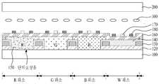
상기 복수 개의 화소는 적색(R) 화소, 녹색(G) 화소, 청색(B) 화소, 및 백색(W) 화소를 포함하여 이루어진다. 도면에는, 각각의 행(row)에서, 적색(R) 화소, 녹색(G) 화소, 청색(B) 화소 및 백색(W) 화소가 그 순서대로 배열된 모습이 도시되어 있지만, 반드시 그와 같은 배열로 한정되는 것은 아니고, 당업계에 공지된 다양한 배열 형태로 변경될 수 있다.The plurality of pixels include a red (R) pixel, a green (G) pixel, a blue (B) pixel, and a white (W) pixel. Although the figure shows a red (R) pixel, a green (G) pixel, a blue (B) pixel and a white (W) pixel arranged in that order in each row, The present invention is not limited to an array, and may be changed into various arrangements known in the art.
도 3은 본 발명의 일 실시예에 따른 액정표시장치의 개략적인 단면도로서, 이는 도 2의 I-I라인의 단면에 해당한다.FIG. 3 is a schematic cross-sectional view of a liquid crystal display according to an embodiment of the present invention, which corresponds to a cross section taken along line I-I of FIG.
도 3에서 알 수 있듯이, 본 발명의 일 실시예에 따른 액정표시장치는, 제1 기판(100), 제2 기판(200), 및 상기 양 기판(100, 200) 사이에 형성된 액정층(300)을 포함하여 이루어진다.3, the liquid crystal display according to an exemplary embodiment of the present invention includes a
상기 제1 기판(100) 상에는, 보다 구체적으로, 상기 제2 기판(200)과 마주하는 상기 제1 기판(100)의 일면 상에는 제1 절연막(120), 데이터 라인(130), 제2 절연막(140), 컬러 필터층(150), 제3 절연막(160), 화소 전극(170) 및 공통 전극(180)이 형성되어 있다.More specifically, a
상기 제1 절연막(120)은 상기 제1 기판(100)의 일면 상에 전체적으로 형성되어 있다.The first insulating
상기 데이터 라인(130)은 상기 제1 절연막(120) 상에 패턴 형성되어 있다. 일측의 데이터 라인(130)과 타측의 데이터 라인(130) 사이 영역에 적색(R) 화소, 녹색(G) 화소, 청색(B) 화소, 또는 백색(W) 화소가 형성된다.The
상기 제2 절연막(140)은 상기 데이터 라인(130) 상에 형성된다. 특히, 상기 제2 절연막(140)은 상기 제1 기판(100)의 일면 상에 전체적으로 형성되어 있다.The second
상기 컬러 필터층(150)은 상기 제2 절연막(140) 상에 형성된다. 상기 컬러 필터층(150)은 적색(R) 화소 내에 형성된 적색(R) 컬러 필터, 녹색(G) 화소 내에 형성된 녹색(G) 컬러 필터, 및 청색(B) 화소 내에 형성된 청색(B) 컬러를 포함하여 이루어진다. 상기 백색(W) 화소 내에는 상기 컬러 필터층(150)이 형성되지 않는다.The
이와 같이, 본 발명의 액정표시장치는 적색(R) 화소, 녹색(G) 화소, 청색(B) 화소, 및 백색(W) 화소의 조합으로 이루어지고, 상기 백색(W) 화소 내에는 컬러 필터층(150)이 형성되지 않기 때문에, 종래에 비하여 컬러 필터로 인한 광투과율 저하 문제가 줄어든다.As described above, the liquid crystal display of the present invention comprises a combination of red (R), green (G), blue (B) and white (W) pixels, The problem of lowering the light transmittance due to the color filter is reduced compared with the related art.
상기 제3 절연막(160)은 상기 컬러 필터층(150) 상에 형성된다. 특히, 상기 제3 절연막(160)은 상기 제1 기판(100)의 일면 상에 전체적으로 형성되어 있다.The third
상기 화소 전극(170) 및 공통 전극(180)은 상기 제3 절연막(160) 상에 패턴 형성되어 있다. 상기 화소 전극(170) 및 공통 전극(180)은 서로 평행하게 배열되어 있어 양자 사이에 수평 전계가 형성되고, 그와 같은 수평 전계에 의해서 상기 액정층(300)의 배열방향이 조절될 수 있다. 이와 같이, 수평 전계에 의해서 상기 액정층(300)의 배열방향이 조절되는 액정표시장치를 수평 전계(In-plane Switching) 모드 액정표시장치라고 칭하며, 본 발명에 따른 액정표시장치는 당업계에 공지된 다양한 형태의 수평 전계 모드 액정표시장치를 포함한다. 즉, 도면에는 상기 화소 전극(170)과 공통 전극(180)이 상기 제3 절연막(160) 상에 패턴 형성된 모습을 도시하였지만, 반드시 그에 한정되는 것은 아니고, 상기 화소 전극(170)과 공통 전극(180)이 서로 상이한 층에 형성될 수도 있다.The
또한, 본 발명에 따른 액정표시장치가 반드시 수평 전계(In-plane Switching) 모드 액정표시장치로 한정되는 것은 아니며, TN(Twisted Nematic) 모드 액정표시장치, FFS(Fringe Field Switching) 모드 액정표시장치, VA(Vertical Alignment) 모드 액정표시장치 등 당업계에 공지된 다양한 액정표시장치를 포함한다.In addition, the liquid crystal display according to the present invention is not limited to the in-plane switching mode liquid crystal display, but may be a twisted nematic (TN) mode liquid crystal display device, an FFS (Fringe Field Switching) And VA (Vertical Alignment) mode liquid crystal display devices.
상기 제2 기판(200) 상에는, 보다 구체적으로, 상기 제1 기판(100)과 마주하는 상기 제2 기판(200)의 일면 상에는 컬러 필터층이 형성되지 않고, 특히, 상기 제2 기판(200)의 일면 상에는 아무런 구성이 형성되지 않을 수 있다. 다만, 반드시 그에 한정되는 것은 아니고, 경우에 따라서, 상기 제2 기판(200)의 일면 상에 블랙 매트릭스(Black Matrix) 및/또는 컬럼 스페이서(Column Spacer)가 형성될 수 있다.More specifically, a color filter layer is not formed on one surface of the
상기 블랙 매트릭스는 화소 영역 이외의 영역으로 광이 투과하는 것을 방지하는 역할을 하는 것이고, 상기 컬럼 스페이서는 액정표시장치의 셀갭(cell gap)을 균일하게 유지시키는 역할을 하는 것이다.The black matrix serves to prevent light from being transmitted to regions other than the pixel region, and the column spacer serves to uniformly maintain the cell gap of the liquid crystal display device.
한편, 상기 블랙 매트릭스(Black Matrix) 및/또는 컬러 스페이서(Column Spacer)는 상기 제2 기판(200) 상에 형성되지 않고, 그 대신에 상기 제1 기판(100) 상에 형성될 수도 있다.Alternatively, the black matrix and / or the column spacer may be formed on the
또한, 상기 TN(Twisted Nematic) 모드 액정표시장치 및 VA(Vertical Alignment) 모드 액정표시장치는 수직 전계에 의해서 액정층(300)의 배열방향이 조절되며, 따라서, 상기 TN(Twisted Nematic) 모드 액정표시장치 및 VA(Vertical Alignment) 모드 액정표시장치의 경우, 상기 공통 전극(180)이 상기 제1 기판(100) 상에 형성되지 않고 그 대신에 상기 제2 기판(200) 상에 형성된다.In the TN (Twisted Nematic) mode liquid crystal display device and the VA (Vertical Alignment) mode liquid crystal display device, the alignment direction of the
한편, 이상과 같은 도 3에 도시한 액정표시장치는 백색(W) 화소 내에 컬러 필터층(150)이 형성되지 않기 때문에, 적색(R)/녹색(G)/청색(B) 화소와 백색(W) 화소 사이에 단차가 발생하게 된다. 이하에서 설명하는 도 4에 따른 액정표시장치는 적색(R)/녹색(G)/청색(B) 화소와 백색(W) 화소 사이의 단차를 최소화한 것이다.3 does not include the
도 4는 본 발명의 다른 실시예에 따른 액정표시장치의 개략적인 단면도로서, 이는 도 2의 I-I라인의 단면에 해당한다.4 is a schematic cross-sectional view of a liquid crystal display device according to another embodiment of the present invention, which corresponds to a cross section of the line I-I in FIG.
도 4에서 알 수 있듯이, 본 발명의 다른 실시예에 따른 액정표시장치는, 제1 기판(100), 제2 기판(200), 및 상기 양 기판(100, 200) 사이에 형성된 액정층(300)을 포함하여 이루어진다. 이하에서는, 전술한 실시예에 동일한 구성에 대한 반복 설명은 생략하기로 한다.4, the liquid crystal display according to another embodiment of the present invention includes a
상기 제1 기판(100) 상에는, 보다 구체적으로, 상기 제2 기판(200)과 마주하는 상기 제1 기판(100)의 일면 상에는 제1 절연막(120), 데이터 라인(130), 제2 절연막(140), 컬러 필터층(150), 제3 절연막(160), 화소 전극(170) 및 공통 전극(180)이 형성되어 있다.More specifically, a first insulating
상기 제1 절연막(120)은 상기 제1 기판(100)의 일면 상에 형성되어 있다.The first insulating
상기 제1 절연막(120)은 백색(W) 화소 내에서는 상기 제1 기판(100)의 일면 전체에 형성되지만, 상기 적색(R)/녹색(G)/청색(B) 화소 내에서는 상기 제1 기판(100)의 일면 전체에 형성되지 않는다. 보다 구체적으로, 상기 제1 절연막(120)은 상기 적색(R) 화소, 녹색(G) 화소, 및 청색(B) 화소에서 단차 보상홀을 구비하도록 형성된다. 따라서, 상기 제1 기판(100)의 일면은 상기 적색(R) 화소, 녹색(G) 화소, 및 청색(B) 화소 내에서는 상기 단차 보상홀에 의해서 외부로 노출되는 반면에, 상기 백색(W) 화소 내에서는 외부로 노출되지 않는다.The first insulating
상기 데이터 라인(130)은 상기 제1 절연막(120) 상에 패턴 형성되어 있다.The
상기 제2 절연막(140)은 상기 데이터 라인(130) 상에 형성된다.The second
상기 제2 절연막(140)은 백색(W) 화소 내에서는 상기 제1 기판(100)의 일면 전체에 형성되지만, 상기 적색(R)/녹색(G)/청색(B) 화소 내에서는 상기 제1 기판(100)의 일면 전체에 형성되지 않는다. 보다 구체적으로, 상기 제2 절연막(140)은 상기 적색(R) 화소, 녹색(G) 화소, 및 청색(B) 화소에서 상기 단차 보상홀을 구비하도록 형성된다. 따라서, 상기 제1 기판(100)의 일면은 상기 적색(R) 화소, 녹색(G) 화소, 및 청색(B) 화소 내에서 상기 단차 보상홀에 의해서 외부로 노출된다.The second
상기 컬러 필터층(150)은 상기 단차 보상홀 내에 형성된다. 보다 구체적으로, 상기 컬러 필터층(150)은 적색(R) 화소 내의 상기 단차 보상홀 내에 형성된 적색(R) 컬러 필터, 녹색(G) 화소 내의 상기 단차 보상홀 내에 형성된 녹색(G) 컬러 필터, 및 청색(B) 화소 내의 상기 단차 보상홀 내에 형성된 청색(B) 컬러를 포함하여 이루어진다. 이와 같은 컬러 필터층(150)은 상기 제1 기판(100)과 접촉하도록 형성된다.The
한편, 도시된 바와 같이, 상기 컬러 필터층(150)이 상기 제2 절연막(140)의 상면 상에 추가로 형성될 수 있다. 또한, 전술한 실시예와 마찬가지로, 상기 백색(W) 화소 내에는 상기 컬러 필터층(150)이 형성되지 않는다.Meanwhile, as shown in the figure, the
상기 제3 절연막(160)은 상기 컬러 필터층(150) 상에 형성된다. 특히, 상기 제3 절연막(160)은 상기 제1 기판(100)의 일면 상에 전체적으로 형성되어 있다.The third
상기 화소 전극(170) 및 공통 전극(180)은 상기 제3 절연막(160) 상에 패턴 형성되어 있다.The
이와 같이, 도 4에 도시한 본 발명의 다른 실시예에 따르면, 컬러 필터층(150)이 적색(R)/녹색(G)/청색(B) 화소 내의 단차 보상홀 내에 형성되기 때문에, 컬러 필터층(150)이 형성되어 있는 적색(R)/녹색(G)/청색(B) 화소와 컬러 필터층(150)이 형성되지 않은 백색(W) 화소 사이에 단차가 최소화될 수 있다.4, since the
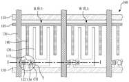
도 5는 본 발명의 일 실시예에 따른 액정표시장치를 구성하는 제1 기판(100)의 보다 상세한 평면도로서, 이는 청색(B) 화소 및 백색(W) 화소를 도시한 것이다. 도시하지는 않았지만, 적색(R) 화소 및 녹색(G) 화소의 구성은 사용되는 컬러 필터를 제외하고 청색(B) 화소의 구성과 동일하다.5 is a more detailed plan view of a
도 5에서 알 수 있듯이, 본 발명의 일 실시예에 따른 제1 기판(100) 상에는 게이트 라인(110), 데이터 라인(130), 박막 트랜지스터(T), 화소 전극(170) 및 공통 전극(180)이 형성되어 있다.5, a
전술한 바와 같이, 상기 게이트 라인(110)과 데이터 라인(130)은 서로 교차 배열되어 복수 개의 화소, 예로서, 청색(B) 화소 및 백색(W) 화소를 정의한다.As described above, the
상기 박막 트랜지스터(T)는 복수 개의 화소 각각에서 상기 게이트 라인(110)과 데이터 라인(130)이 교차하는 영역에 형성된다. 상기 박막 트랜지스터(T)는 게이트 전극(115), 소스 전극(132), 및 드레인 전극(134)을 포함하여 이루어진다. 상기 게이트 전극(115)은 상기 게이트 라인(110)에서 분기되어 있고, 상기 소스 전극(132)은 상기 데이터 라인(130)에서 분기되어 있고, 상기 드레인 전극(134)은 상기 소스 전극(132)과 마주하면서 이격되어 있다. 이와 같은 박막 트랜지스터(T)는 당업계에 공지된 다양한 형태로 변경될 수 있으며, 예를 들어, 게이트 전극(115)이 반도체층 아래에 형성되는 바텀 게이트(Bottom Gate) 구조뿐만 아니라 게이트 전극(115)이 반도체층 위에 형성된 탑 게이트(Top Gate) 구조로 형성될 수도 있다.The thin film transistor T is formed in a region where the
상기 화소 전극(170)은 복수 개의 화소 각각에서 콘택홀(CH)을 통해서 상기 박막 트랜지스터(T)의 드레인 전극(134)과 연결되어 있다.The
상기 공통 전극(180)은 복수 개의 화소 각각에서 상기 화소 전극(170)과 평행하게 배열되어 있으며, 이와 같은 공통 전극(180)은 공통 라인(185)과 연결되어 있다. 구체적으로 도시하지는 않았지만, 상기 공통 전극(180)과 공통 라인(185)은 서로 상이한 층에 형성될 수 있고, 이 경우, 소정의 콘택홀을 통해서 상기 공통 전극(180)과 공통 라인(185)이 서로 연결된다.The
도 6은 본 발명의 일 실시예에 따른 액정표시장치의 단면도로서, 이는 도 5의 I-I라인의 단면에 해당한다.FIG. 6 is a cross-sectional view of a liquid crystal display device according to an embodiment of the present invention, which corresponds to a cross section taken along the line I-I of FIG.
도 6에서 알 수 있듯이, 본 발명의 일 실시예에 따른 액정표시장치는 제1 기판(100), 상기 제1 기판(100)과 마주하는 제2 기판(200), 및 상기 제1 기판(100)과 제2 기판(200) 사이에 형성된 액정층(300)을 포함하여 이루어진다.6, the liquid crystal display according to an exemplary embodiment of the present invention includes a
상기 제1 기판(100) 상에는 게이트 전극(115)이 패턴 형성되어 있다. 상기 게이트 전극(115)은 청색(B) 화소 및 백색(W) 화소에 각각 패턴 형성되어 있다.A
상기 게이트 전극(115) 상에는 제1 절연막(120)이 형성되어 있다. 상기 제1 절연막(120)은 백색(W) 화소 내에서는 상기 제1 기판(100)의 일면 전체에 형성되지만, 상기 청색(B) 화소 내에서는 단차 보상홀을 구비하도록 형성된다.A first insulating
상기 제1 절연막(120) 상에는 반도체층(125)이 패턴 형성되어 있다. 상기 반도체층(125)은 청색(B) 화소 및 백색(W) 화소에 각각 패턴 형성되어 있다.A
상기 반도체층(125) 상에는 소스 전극(132) 및 드레인 전극(134)이 패턴 형성되어 있다. 상기 소스 전극(132) 및 드레인 전극(134)은 청색(B) 화소 및 백색(W) 화소에 각각 패턴 형성되어 있다. 또한, 상기 소스 전극(132)은 데이터 라인(130)에 연결된다.A
상기 소스 전극(132) 및 드레인 전극(134) 상에는 제2 절연막(140)이 형성되어 있다. 상기 제2 절연막(140)은 백색(W) 화소 내에서는 후술하는 콘택홀(CH)을 제외하고 상기 제1 기판(100)의 일면 전체에 형성되지만, 상기 청색(B) 화소 내에서는 후술하는 콘택홀(CH)과 더불어 상기 단차 보상홀을 구비하도록 형성된다.A second insulating
상기 단차 보상홀 내에는 컬러 필터층(150)이 형성되어 있다.A
상기 컬러 필터층(150)은 상기 청색(B) 화소 내의 단차 보상홀 내에 형성되어 있으며, 특히, 상기 단차 보상홀 내에서부터 상기 제2 절연막(140)의 상면까지 연장되어 있다. 따라서, 상기 컬러 필터층(150)은 박막 트랜지스터와 오버랩되도록 형성될 수 있다.The
상기 컬러 필터층(150)은 상기 백색(W) 화소에는 형성되지 않는다. 다만, 반드시 그에 한정되는 것은 아니고, 상기 컬러 필터층(150)이 상기 백색(W) 화소 내의 박막 트랜지스터와 오버랩되도록 형성될 수 있다. 즉, 전술한 도 5를 참조하면, 상기 백색(W) 화소는 게이트 라인(110)과 데이터 라인(130)에 의해서 정의되는 것으로서, 상기 백색(W) 화소 내에는 박막 트랜지스터(T)가 형성된 영역과 그렇지 않은 영역이 있다. 이때, 상기 박막 트랜지스터(T)가 형성된 영역은 광이 차단되는 영역이므로, 그 영역에 컬러 필터층(150)이 형성되어도 무방하다.The
상기 청색(B) 화소에 형성된 컬러 필터층(150) 및 상기 백색(W) 화소에 형성된 제2 절연막(140) 상에는 제3 절연막(160)이 형성되어 있다.A third insulating
상기 청색(B) 화소의 경우, 상기 제2 절연막(140), 컬러 필터층(150) 및 제3 절연막(160)에 콘택홀(CH)이 형성되어 있고, 상기 콘택홀(CH)에 의해서 상기 드레인 전극(134)의 소정 영역이 노출된다.In the case of the blue (B) pixel, a contact hole CH is formed in the second insulating
상기 백색(W) 화소의 경우, 상기 제2 절연막(140) 및 제3 절연막(160)에 콘택홀(CH)이 형성되어 있고, 상기 콘택홀(CH)에 의해서 상기 드레인 전극(134)의 소정 영역이 노출된다. 한편, 상기 컬러 필터층(150)이 상기 백색(W) 화소 내의 박막 트랜지스터(T)와 오버랩되도록 형성된 경우, 상기 백색(W) 화소 내의 컬러 필터층에도 콘택홀(CH)이 형성된다.In the case of the white (W) pixel, a contact hole CH is formed in the second insulating
상기 제3 절연막(160) 상에는 화소 전극(170)이 패턴 형성되어 있다. 상기 화소 전극(170)은 청색(B) 화소 및 백색(W) 화소에 각각 형성되며, 특히, 상기 콘택홀(CH)을 통해서 상기 드레인 전극(134)과 연결된다.A
도 7a 내지 도 7g는 본 발명의 일 실시예에 따른 액정표시장치의 제조 공정을 도시한 개략적인 공정 단면도로서, 이는 전술한 도 6에 따른 액정표시장치의 제조 공정에 관한 것이다.7A to 7G are schematic process sectional views illustrating a manufacturing process of a liquid crystal display device according to an embodiment of the present invention, which relates to the manufacturing process of the liquid crystal display device according to FIG.
전술한 바와 마찬가지로, 이하에는 청색(B) 화소 및 백색(W) 화소의 제조 공정에 대해서 도시하며, 적색(R) 화소 및 녹색(G) 화소의 제조 공정은 사용되는 컬러 필터를 제외하고 청색(B) 화소의 제조 공정과 동일하다.The manufacturing process of the red (R) pixel and the green (G) pixel is the same as the manufacturing process of the blue (B) pixel and the white B) pixel.
우선, 도 7a에서 알 수 있듯이, 제1 기판(100) 상에 게이트 전극(115)을 형성하고, 상기 게이트 전극(115) 상에 제1 절연막층(120a)을 형성하고, 상기 제1 절연막층(120a) 상에 반도체층(125)을 형성하고, 상기 반도체층(125) 상에 데이터 라인(130), 소스 전극(132) 및 드레인 전극(134)을 형성한다.7A, a
상기 게이트 전극(115)은 청색(B) 화소 및 백색(W) 화소에 각각 패턴 형성한다.The
상기 제1 절연막층(120a)은 상기 제1 기판(100) 상에 전체적으로 형성한다.The first insulating
상기 반도체층(125), 소스 전극(132) 및 드레인 전극(134)은 청색(B) 화소 및 백색(W) 화소에 각각 패턴 형성한다.The
한편, 도시된 바와 같이, 상기 게이트 전극(115)이 상기 반도체층(125) 아래에 형성될 수도 있지만(바텀 게이트 구조), 상기 게이트 전극(115)이 반도체층(125) 위에 형성될 수도 있다(탑 게이트 구조).The
다음, 도 7b에서 알 수 있듯이, 상기 소스 전극(132) 및 드레인 전극(134) 상에 제2 절연막층(140a)을 형성하고, 상기 제2 절연막층(140a) 상에 포토 레지스트 패턴(145)을 형성한다.7B, a second insulating
상기 제2 절연막층(140a)은 상기 제1 기판(100) 상에 전체적으로 형성한다.The second insulating
상기 포토 레지스트 패턴(145)은 제1 개구부(P1) 및 제2 개구부(P2)를 포함하고 있다.The
상기 제1 개구부(P1)는 후술하는 콘택홀(CH)에 대응하는 것으로서 청색(B) 화소 및 백색(W) 화소 각각에서 박막 트랜지스터의 드레인 전극(134)과 오버랩되도록 형성된다.The first opening P1 corresponds to the contact hole CH to be described later and overlaps with the
상기 제2 개구부(P2)는 후술하는 단차 보상홀에 대응하는 것으로서 청색(B) 화소에는 형성되지만 백색(W) 화소에는 형성되지 않는다. 상기 제2 개구부(P2)는 청색(B) 화소 내에서 박막 트랜지스터가 형성되지 않은 영역과 오버랩되도록 형성된다.The second opening P2 corresponds to the step difference compensation hole to be described later and is formed in the blue (B) pixel, but not in the white (W) pixel. The second opening P2 is formed so as to overlap with a region where the thin film transistor is not formed in the blue (B) pixel.
다음, 도 7c에서 알 수 있듯이, 포토 레지스트 패턴(145)을 마스크로 하여 상기 제2 절연막층(140a) 및 제1 절연막층(120a)을 식각하여 제2 절연막(140) 및 제1 절연막(120)을 패턴 형성하고, 그 후, 포토 레지스트 패턴(145)을 제거한다.7C, the second insulating
즉, 상기 제2 절연막(140)은 청색(B) 화소 및 백색(W) 화소 각각에서 콘택홀(CH)을 구비하여, 상기 콘택홀(CH)을 통해서 드레인 전극(134)이 외부로 노출된다. 또한, 상기 제2 절연막(140) 및 제1 절연막(120)은 상기 청색(B) 화소에서 단차 보상홀을 구비하여, 상기 단차 보상홀을 통해서 제1 기판(100)이 외부로 노출된다.That is, the second insulating
다음, 도 7d에서 알 수 있듯이, 상기 청색(B) 화소의 단차 보상홀 내에 컬러 필터층(150)을 형성한다.7D, a
상기 컬러 필터층(150)은 상기 단차 보상홀 내에서부터 상기 제2 절연막(140)의 상면까지 연장되어 박막 트랜지스터와 오버랩되도록 형성된다. 이때, 상기 컬러 필터층(150)은 콘택홀(CH)을 구비하도록 형성한다.The
한편, 도시하지는 않았지만, 상기 백색(W) 화소 내의 박막 트랜지스터와 오버랩되도록 컬러 필터층(150)을 추가로 형성할 수도 있다.Although not shown, the
다음, 도 7e에서 알 수 있듯이, 청색(B) 화소에 형성된 컬러 필터층(150) 및 백색(W) 화소에 형성된 제2 절연막(140) 상에 제3 절연막(160)을 형성한다.7E, a third
상기 제3 절연막(160)은 청색(B) 화소 및 백색(W) 화소 각각에서 콘택홀(CH)을 구비하도록 형성한다.The third
다음, 도 7f에서 알 수 있듯이, 상기 제3 절연막(160) 상에 화소 전극(170)을 형성한다. 상기 화소 전극(170)은 청색(B) 화소 및 백색(W) 화소에 각각 패턴 형성하며, 특히, 상기 콘택홀(CH)을 통해서 상기 드레인 전극(134)과 연결되도록 형성한다.Next, as shown in FIG. 7F, the
다음, 도 7g에서 알 수 있듯이, 액정층(300)을 사이에 두고 상기 제1 기판(100)과 제2 기판(200)을 합착한다.Next, as shown in FIG. 7G, the
상기 제1 기판(100)과 제2 기판(200)의 합착은 당업계에 공지된 진공주입법 또는 액정적하법을 이용하여 수행할 수 있다.The
100: 제1 기판 110: 게이트 라인
120: 제1 절연막 130: 데이터 라인
140: 제2 절연막 150: 컬러 필터층
160: 제3 절연막 170: 화소 전극
180: 공통 전극 200: 제2 기판
300: 액정층100: first substrate 110: gate line
120: first insulating film 130: data line
140: second insulating film 150: color filter layer
160: Third insulating film 170: Pixel electrode
180: common electrode 200: second substrate
300: liquid crystal layer
Claims (9)
Translated fromKorean상기 제1 기판과 마주하는 제2 기판;
상기 제1 기판과 제2 기판 사이에 형성된 액정층;
상기 제1 기판 상의 적색 화소, 녹색 화소, 청색 화소, 및 백색 화소 각각에 형성된 박막 트랜지스터; 및
상기 제1 기판 상에 형성된 컬러 필터층을 포함하여 이루어지고,
상기 컬러 필터층은 상기 적색 화소 내에 형성된 적색 컬러 필터, 상기 녹색 화소 내에 형성된 녹색 컬러 필터 및 상기 청색 화소 내에 형성된 청색 컬러 필터로 이루어지고,
상기 컬러 필터층은 상기 제1 기판 상의 절연막 내에 구비된 단차 보상홀 내에 형성된 것을 특징으로 하는 액정표시장치.A first substrate including a red pixel, a green pixel, a blue pixel, and a white pixel;
A second substrate facing the first substrate;
A liquid crystal layer formed between the first substrate and the second substrate;
A thin film transistor formed on each of the red pixel, the green pixel, the blue pixel, and the white pixel on the first substrate; And
And a color filter layer formed on the first substrate,
Wherein the color filter layer comprises a red color filter formed in the red pixel, a green color filter formed in the green pixel, and a blue color filter formed in the blue pixel,
And the color filter layer is formed in the step difference compensation hole provided in the insulating film on the first substrate.
상기 컬러 필터층은 상기 제1 기판과 접촉하도록 형성된 것을 특징으로 하는 액정표시장치.The method according to claim 1,
And the color filter layer is formed to be in contact with the first substrate.
상기 박막 트랜지스터는 게이트 전극, 소스 전극, 및 드레인 전극을 포함하여 이루어지고, 상기 절연막은 상기 게이트 전극 상에 형성된 제1 절연막 및 상기 소스 전극과 드레인 전극 상에 형성된 제2 절연막으로 이루어진 것을 특징으로 하는 액정표시장치.The method according to claim 1,
Wherein the thin film transistor includes a gate electrode, a source electrode, and a drain electrode, wherein the insulating film is composed of a first insulating film formed on the gate electrode and a second insulating film formed on the source electrode and the drain electrode Liquid crystal display device.
상기 절연막은 상기 백색 화소 내에서 상기 기판 상에 전체적으로 형성된 것을 특징으로 하는 액정표시장치.The method according to claim 1,
Wherein the insulating film is formed entirely on the substrate in the white pixel.
상기 컬러 필터층은 상기 박막 트랜지스터와 오버랩되도록 형성된 것을 특징으로 하는 액정표시장치.The method according to claim 1,
And the color filter layer is formed to overlap with the thin film transistor.
상기 컬러 필터층은 그 내부에 콘택홀이 형성되어 있고, 상기 콘택홀을 통해서 상기 박막 트랜지스터의 드레인 전극이 노출되는 것을 특징으로 하는 액정표시장치.6. The method of claim 5,
Wherein the color filter layer has a contact hole formed therein, and a drain electrode of the thin film transistor is exposed through the contact hole.
상기 소스 전극 및 드레인 전극 상에 제2 절연막층을 형성하고, 상기 제2 절연막층 상에 포토 레지스트 패턴을 형성하는 공정;
상기 포토 레지스트 패턴을 마스크로 하여 상기 제2 절연막층 및 제1 절연막층을 식각하여, 상기 제1 기판이 노출되도록 단차 보상홀을 구비한 제2 절연막 및 제1 절연막을 형성하는 공정;
상기 단차 보상홀 내에 컬러 필터층을 형성하는 공정; 및
액정층을 사이에 두고 상기 제1 기판과 제2 기판을 합착하는 공정을 포함하여 이루어진 액정표시장치의 제조방법.A step of forming a first insulating film layer on the first substrate and a source electrode and a drain electrode on the first insulating film layer;
Forming a second insulating film layer on the source electrode and the drain electrode, and forming a photoresist pattern on the second insulating film layer;
Etching the second insulating film layer and the first insulating film layer using the photoresist pattern as a mask to form a second insulating film and a first insulating film having step difference compensation holes so that the first substrate is exposed;
Forming a color filter layer in the step difference compensation hole; And
And bonding the first substrate and the second substrate to each other with the liquid crystal layer interposed therebetween.
상기 제1 기판은 적색 화소, 녹색 화소, 청색 화소, 및 백색 화소를 포함하여 이루어지고, 상기 단차 보상홀은 상기 적색 화소, 녹색 화소 및 청색 화소 내에 형성하는 것을 특징으로 하는 액정표시장치의 제조방법.8. The method of claim 7,
Wherein the first substrate includes a red pixel, a green pixel, a blue pixel, and a white pixel, and the step difference compensation hole is formed in the red pixel, the green pixel, and the blue pixel. .
상기 컬러 필터층은 상기 단차 보상홀 내에서부터 상기 제2 절연막의 상면까지 연장되며, 그 내부에 콘택홀을 구비하도록 형성하는 것을 특징으로 하는 액정표시장치의 제조방법.9. The method of claim 8,
Wherein the color filter layer extends from the step difference compensation hole to the upper surface of the second insulating film and includes a contact hole therein.
Priority Applications (1)
| Application Number | Priority Date | Filing Date | Title |
|---|---|---|---|
| KR1020130010278AKR102043862B1 (en) | 2013-01-30 | 2013-01-30 | Liquid Crystal Display Device and Method of manufacturing the sames |
Applications Claiming Priority (1)
| Application Number | Priority Date | Filing Date | Title |
|---|---|---|---|
| KR1020130010278AKR102043862B1 (en) | 2013-01-30 | 2013-01-30 | Liquid Crystal Display Device and Method of manufacturing the sames |
Publications (2)
| Publication Number | Publication Date |
|---|---|
| KR20140097782Atrue KR20140097782A (en) | 2014-08-07 |
| KR102043862B1 KR102043862B1 (en) | 2019-12-02 |
Family
ID=51744915
Family Applications (1)
| Application Number | Title | Priority Date | Filing Date |
|---|---|---|---|
| KR1020130010278AActiveKR102043862B1 (en) | 2013-01-30 | 2013-01-30 | Liquid Crystal Display Device and Method of manufacturing the sames |
Country Status (1)
| Country | Link |
|---|---|
| KR (1) | KR102043862B1 (en) |
Cited By (3)
| Publication number | Priority date | Publication date | Assignee | Title |
|---|---|---|---|---|
| KR20170074410A (en)* | 2015-12-22 | 2017-06-30 | 엘지디스플레이 주식회사 | Liquid Crystal Display Device And Method Of Fabricating The Same |
| KR20170129512A (en)* | 2016-05-17 | 2017-11-27 | 엘지디스플레이 주식회사 | Organic light emitting display device and method for fabricating the same |
| KR101875695B1 (en)* | 2015-11-30 | 2018-07-06 | 엘지디스플레이 주식회사 | Array Substrate For Liquid Crystal Display Device And Method Of Fabricating The Same |
Citations (5)
| Publication number | Priority date | Publication date | Assignee | Title |
|---|---|---|---|---|
| KR100397399B1 (en)* | 2001-02-22 | 2003-09-13 | 엘지.필립스 엘시디 주식회사 | transflective liquid crystal display and manufacturing method thereof |
| KR20040080778A (en)* | 2003-03-13 | 2004-09-20 | 삼성전자주식회사 | Liquid crystal displays using 4 color and panel for the same |
| KR20060079061A (en)* | 2004-12-31 | 2006-07-05 | 엘지.필립스 엘시디 주식회사 | LCD and its manufacturing method |
| KR20060120878A (en)* | 2005-05-23 | 2006-11-28 | 엘지.필립스 엘시디 주식회사 | LCD and its manufacturing method |
| KR20080025552A (en)* | 2006-09-18 | 2008-03-21 | 삼성전자주식회사 | Thin film transistor substrate, manufacturing method thereof and liquid crystal display panel having same |
- 2013
- 2013-01-30KRKR1020130010278Apatent/KR102043862B1/enactiveActive
Patent Citations (5)
| Publication number | Priority date | Publication date | Assignee | Title |
|---|---|---|---|---|
| KR100397399B1 (en)* | 2001-02-22 | 2003-09-13 | 엘지.필립스 엘시디 주식회사 | transflective liquid crystal display and manufacturing method thereof |
| KR20040080778A (en)* | 2003-03-13 | 2004-09-20 | 삼성전자주식회사 | Liquid crystal displays using 4 color and panel for the same |
| KR20060079061A (en)* | 2004-12-31 | 2006-07-05 | 엘지.필립스 엘시디 주식회사 | LCD and its manufacturing method |
| KR20060120878A (en)* | 2005-05-23 | 2006-11-28 | 엘지.필립스 엘시디 주식회사 | LCD and its manufacturing method |
| KR20080025552A (en)* | 2006-09-18 | 2008-03-21 | 삼성전자주식회사 | Thin film transistor substrate, manufacturing method thereof and liquid crystal display panel having same |
Cited By (3)
| Publication number | Priority date | Publication date | Assignee | Title |
|---|---|---|---|---|
| KR101875695B1 (en)* | 2015-11-30 | 2018-07-06 | 엘지디스플레이 주식회사 | Array Substrate For Liquid Crystal Display Device And Method Of Fabricating The Same |
| KR20170074410A (en)* | 2015-12-22 | 2017-06-30 | 엘지디스플레이 주식회사 | Liquid Crystal Display Device And Method Of Fabricating The Same |
| KR20170129512A (en)* | 2016-05-17 | 2017-11-27 | 엘지디스플레이 주식회사 | Organic light emitting display device and method for fabricating the same |
Also Published As
| Publication number | Publication date |
|---|---|
| KR102043862B1 (en) | 2019-12-02 |
Similar Documents
| Publication | Publication Date | Title |
|---|---|---|
| US8350792B2 (en) | Display device | |
| US10332917B2 (en) | Pixel unit and method for producing the same, array substrate and display apparatus | |
| CN103676333B (en) | Filter substrate and the liquid crystal indicator including this filter substrate | |
| KR101352113B1 (en) | Liquid Crystal Display Panel Of Horizontal Electronic Fileld Applying Type and Method of Fabricating the same | |
| JP4889388B2 (en) | Liquid crystal display | |
| US9239501B2 (en) | Liquid crystal display device | |
| JP5275861B2 (en) | Liquid crystal display device and electronic device | |
| KR101495467B1 (en) | Array substrate, liquid crystal display panel and driving method | |
| KR101835545B1 (en) | Liquid crystal display device and Method for manufacturing the same | |
| JP5292612B2 (en) | Liquid crystal display | |
| JP2017111327A (en) | Liquid crystal display | |
| JP6554403B2 (en) | Liquid crystal display | |
| JP4092309B2 (en) | Liquid crystal display | |
| KR100669377B1 (en) | Liquid Crystal Display and Manufacturing Method Thereof | |
| KR102089590B1 (en) | Liquid crystal display and manufacturing method thereof | |
| KR101697759B1 (en) | Liquid crystal display | |
| KR102009477B1 (en) | Method for manufacturing Liquid crystal display device | |
| KR102043862B1 (en) | Liquid Crystal Display Device and Method of manufacturing the sames | |
| KR20130034277A (en) | Liquid crystal display device and method for manufacturing the same | |
| TWI422910B (en) | Liquid crystal display panel | |
| US20140168045A1 (en) | Array substrate, liquid crystal display panel and driving method | |
| KR20140112289A (en) | Liquid crystal display and manufacturing method thereof | |
| KR20190061328A (en) | Display device | |
| JP2018205601A (en) | LCD panel | |
| KR20070088044A (en) | Array substrate of liquid crystal display device and manufacturing method thereof |
Legal Events
| Date | Code | Title | Description |
|---|---|---|---|
| PA0109 | Patent application | Patent event code:PA01091R01D Comment text:Patent Application Patent event date:20130130 | |
| PG1501 | Laying open of application | ||
| A201 | Request for examination | ||
| PA0201 | Request for examination | Patent event code:PA02012R01D Patent event date:20180110 Comment text:Request for Examination of Application Patent event code:PA02011R01I Patent event date:20130130 Comment text:Patent Application | |
| E902 | Notification of reason for refusal | ||
| PE0902 | Notice of grounds for rejection | Comment text:Notification of reason for refusal Patent event date:20181113 Patent event code:PE09021S01D | |
| E902 | Notification of reason for refusal | ||
| PE0902 | Notice of grounds for rejection | Comment text:Notification of reason for refusal Patent event date:20190507 Patent event code:PE09021S01D | |
| E701 | Decision to grant or registration of patent right | ||
| PE0701 | Decision of registration | Patent event code:PE07011S01D Comment text:Decision to Grant Registration Patent event date:20191105 | |
| GRNT | Written decision to grant | ||
| PR0701 | Registration of establishment | Comment text:Registration of Establishment Patent event date:20191106 Patent event code:PR07011E01D | |
| PR1002 | Payment of registration fee | Payment date:20191107 End annual number:3 Start annual number:1 | |
| PG1601 | Publication of registration | ||
| PR1001 | Payment of annual fee | Payment date:20221017 Start annual number:4 End annual number:4 | |
| PR1001 | Payment of annual fee | Payment date:20231016 Start annual number:5 End annual number:5 | |
| PR1001 | Payment of annual fee | Payment date:20241015 Start annual number:6 End annual number:6 |