KR20140095152A - Display device - Google Patents
Display deviceDownload PDFInfo
- Publication number
- KR20140095152A KR20140095152AKR1020130007567AKR20130007567AKR20140095152AKR 20140095152 AKR20140095152 AKR 20140095152AKR 1020130007567 AKR1020130007567 AKR 1020130007567AKR 20130007567 AKR20130007567 AKR 20130007567AKR 20140095152 AKR20140095152 AKR 20140095152A
- Authority
- KR
- South Korea
- Prior art keywords
- touch
- touch sensors
- base substrate
- gate
- disposed
- Prior art date
- Legal status (The legal status is an assumption and is not a legal conclusion. Google has not performed a legal analysis and makes no representation as to the accuracy of the status listed.)
- Withdrawn
Links
Images


Classifications
- G—PHYSICS
- G06—COMPUTING OR CALCULATING; COUNTING
- G06F—ELECTRIC DIGITAL DATA PROCESSING
- G06F3/00—Input arrangements for transferring data to be processed into a form capable of being handled by the computer; Output arrangements for transferring data from processing unit to output unit, e.g. interface arrangements
- G06F3/01—Input arrangements or combined input and output arrangements for interaction between user and computer
- G06F3/03—Arrangements for converting the position or the displacement of a member into a coded form
- G06F3/041—Digitisers, e.g. for touch screens or touch pads, characterised by the transducing means
- G06F3/0412—Digitisers structurally integrated in a display
- G—PHYSICS
- G06—COMPUTING OR CALCULATING; COUNTING
- G06F—ELECTRIC DIGITAL DATA PROCESSING
- G06F3/00—Input arrangements for transferring data to be processed into a form capable of being handled by the computer; Output arrangements for transferring data from processing unit to output unit, e.g. interface arrangements
- G06F3/01—Input arrangements or combined input and output arrangements for interaction between user and computer
- G06F3/03—Arrangements for converting the position or the displacement of a member into a coded form
- G06F3/041—Digitisers, e.g. for touch screens or touch pads, characterised by the transducing means
- G06F3/0416—Control or interface arrangements specially adapted for digitisers
- G06F3/04166—Details of scanning methods, e.g. sampling time, grouping of sub areas or time sharing with display driving
- G—PHYSICS
- G06—COMPUTING OR CALCULATING; COUNTING
- G06F—ELECTRIC DIGITAL DATA PROCESSING
- G06F3/00—Input arrangements for transferring data to be processed into a form capable of being handled by the computer; Output arrangements for transferring data from processing unit to output unit, e.g. interface arrangements
- G06F3/01—Input arrangements or combined input and output arrangements for interaction between user and computer
- G06F3/03—Arrangements for converting the position or the displacement of a member into a coded form
- G06F3/041—Digitisers, e.g. for touch screens or touch pads, characterised by the transducing means
- G06F3/044—Digitisers, e.g. for touch screens or touch pads, characterised by the transducing means by capacitive means
- G06F3/0443—Digitisers, e.g. for touch screens or touch pads, characterised by the transducing means by capacitive means using a single layer of sensing electrodes
- G—PHYSICS
- G06—COMPUTING OR CALCULATING; COUNTING
- G06F—ELECTRIC DIGITAL DATA PROCESSING
- G06F3/00—Input arrangements for transferring data to be processed into a form capable of being handled by the computer; Output arrangements for transferring data from processing unit to output unit, e.g. interface arrangements
- G06F3/01—Input arrangements or combined input and output arrangements for interaction between user and computer
- G06F3/03—Arrangements for converting the position or the displacement of a member into a coded form
- G06F3/041—Digitisers, e.g. for touch screens or touch pads, characterised by the transducing means
- G06F3/044—Digitisers, e.g. for touch screens or touch pads, characterised by the transducing means by capacitive means
- G06F3/0446—Digitisers, e.g. for touch screens or touch pads, characterised by the transducing means by capacitive means using a grid-like structure of electrodes in at least two directions, e.g. using row and column electrodes
- G—PHYSICS
- G06—COMPUTING OR CALCULATING; COUNTING
- G06F—ELECTRIC DIGITAL DATA PROCESSING
- G06F3/00—Input arrangements for transferring data to be processed into a form capable of being handled by the computer; Output arrangements for transferring data from processing unit to output unit, e.g. interface arrangements
- G06F3/01—Input arrangements or combined input and output arrangements for interaction between user and computer
- G06F3/03—Arrangements for converting the position or the displacement of a member into a coded form
- G06F3/041—Digitisers, e.g. for touch screens or touch pads, characterised by the transducing means
- G06F3/044—Digitisers, e.g. for touch screens or touch pads, characterised by the transducing means by capacitive means
- G06F3/0448—Details of the electrode shape, e.g. for enhancing the detection of touches, for generating specific electric field shapes, for enhancing display quality
- G—PHYSICS
- G09—EDUCATION; CRYPTOGRAPHY; DISPLAY; ADVERTISING; SEALS
- G09G—ARRANGEMENTS OR CIRCUITS FOR CONTROL OF INDICATING DEVICES USING STATIC MEANS TO PRESENT VARIABLE INFORMATION
- G09G3/00—Control arrangements or circuits, of interest only in connection with visual indicators other than cathode-ray tubes
- G09G3/20—Control arrangements or circuits, of interest only in connection with visual indicators other than cathode-ray tubes for presentation of an assembly of a number of characters, e.g. a page, by composing the assembly by combination of individual elements arranged in a matrix no fixed position being assigned to or needed to be assigned to the individual characters or partial characters
Landscapes
- Engineering & Computer Science (AREA)
- Theoretical Computer Science (AREA)
- General Engineering & Computer Science (AREA)
- Physics & Mathematics (AREA)
- General Physics & Mathematics (AREA)
- Human Computer Interaction (AREA)
- Quality & Reliability (AREA)
- Computer Hardware Design (AREA)
- Liquid Crystal (AREA)
- Devices For Indicating Variable Information By Combining Individual Elements (AREA)
- Position Input By Displaying (AREA)
Abstract
Translated fromKorean
Description
Translated fromKorean본 발명은 표시장치에 관한 것으로, 상세하게는 터치 이벤트를 감지할 수 있는 표시장치에 관한 것이다.The present invention relates to a display device, and more particularly to a display device capable of sensing a touch event.
터치패널은 터치 이벤트가 발생한 지점(이하, 터치지점)의 좌표정보를 획득하는 입력수단이다. 상기 터치패널은 키보드 및 마우스와 같은 입력 장치를 대체한다.The touch panel is input means for obtaining coordinate information of a point (hereinafter referred to as a touch point) at which a touch event occurs. The touch panel replaces an input device such as a keyboard and a mouse.
상기 터치패널은 그 동작원리에 따라 저항막 방식, 정전용량 방식, 전자기 유도방식으로 나뉜다. 상기 정전용량 방식의 상기 터치패널은 기능에 따라 구분되는 입력 터치전극과 출력 터치전극을 포함한다. 상기 입력 터치전극과 상기 출력 터치전극은 서로 절연되게 교차한다.The touch panel is divided into a resistance film type, a capacitance type, and an electromagnetic induction type according to its operation principle. The touch panel of the capacitive type includes an input touch electrode and an output touch electrode that are classified according to functions. The input touch electrode and the output touch electrode are insulated from each other.
일반적으로 상기 터치패널은 표시패널의 외부에 부착된다. 상기 표시패널은 상기 터치패널로부터 수신된 좌표정보에 대응하는 영상을 표시한다. 상기 표시패널에 부착된 상기 터치패널은 상기 표시장치의 두께를 증가시킨다. 별도로 제조된 상기 터치패널은 상기 표시장치의 비용을 증가시킨다.Generally, the touch panel is attached to the outside of the display panel. The display panel displays an image corresponding to the coordinate information received from the touch panel. The touch panel attached to the display panel increases the thickness of the display device. The separately manufactured touch panel increases the cost of the display device.
따라서, 본 발명은 터치 패널 기능이 부가된 표시장치를 제공하는 것을 목적으로 한다.Accordingly, it is an object of the present invention to provide a display device to which a touch panel function is added.
본 발명의 일 실시예에 따른 표시장치는 제1 베이스 기판, 복수 개의 게이트 라인들, 복수 개의 화소들, 복수 개의 터치센서들 및 터치감지부를 포함한다. 상기 제1 베이스 기판은 터치면을 제공하고, 차광영역과 복수 개의 화소영역들로 구분된다. 상기 복수 개의 게이트 라인들은 상기 제1 베이스 기판 상에 배치되고, 제1 방향으로 연장되며 상기 제1 방향과 교차하는 제2 방향으로 배열되고, 활성화 구간이 서로 다른 게이트 신호들을 각각 수신한다.A display device according to an embodiment of the present invention includes a first base substrate, a plurality of gate lines, a plurality of pixels, a plurality of touch sensors, and a touch sensing unit. The first base substrate provides a touch surface, and is divided into a light shielding region and a plurality of pixel regions. The plurality of gate lines are arranged on the first base substrate and arranged in a second direction extending in a first direction and intersecting the first direction, respectively, and receiving gate signals having different activation periods.
상고 복수 개의 화소들은 상기 복수 개의 화소영역들에 대응하게 배치되며, 상기 게이트 신호들에 응답하여 활성화된다. 상기 복수 개의 터치센서들은 상기 제1 베이스 기판 상에 배치되고, 상기 게이트 신호들을 감지신호들로 이용하여 상기 복수 개의 게이트 라인들과 정전결합된다. 상기 터치 감지부는 상기 복수 개의 터치센서들로부터 제공된 출력신호들로부터 터치지점의 좌표정보를 산출한다.The plurality of pixels are arranged corresponding to the plurality of pixel regions, and are activated in response to the gate signals. The plurality of touch sensors are disposed on the first base substrate and are electrostatically coupled to the plurality of gate lines using the gate signals as sense signals. The touch sensing unit calculates coordinate information of a touch point from output signals provided from the plurality of touch sensors.
상기 복수 개의 터치센서들은, 상기 제2 방향으로 연장된 형상으로, 상기 제1 방향의 너비는 상기 제2 방향을 따라 변경된다.The plurality of touch sensors may have a shape extending in the second direction, and the width of the first direction may be changed along the second direction.
상기 복수 개의 터치센서들은, 상기 제2 방향을 따라 상기 제1 방향의 너비가 증가되는 제1 터치센서들 및 상기 제2 방향을 따라 상기 제1 방향의 너비가 감소되는 제2 터치센서들을 포함한다.The plurality of touch sensors include first touch sensors whose widths in the first direction are increased along the second direction and second touch sensors whose widths in the first direction are decreased along the second direction .
상기 제1 터치센서들 및 상기 제2 터치센서들은 교번하게 배치된다. 상기 출력신호들 각각은 상기 게이트 신호들에 근거하여 생성된 레벨이 다른 복수 개의 펄스들을 포함한다.The first touch sensors and the second touch sensors are alternately arranged. Each of the output signals includes a plurality of pulses having different levels generated based on the gate signals.
상기 터치 감지부는 상기 복수 개의 펄스들의 변화된 레벨에 근거하여 상기 터치지점의 상기 제2 방향의 좌표정보를 산출한다. 상기 터치 감지부는 상기 복수 개의 펄스들 중 일부의 펄스들에 근거하여 상기 터치지점의 좌표정보를 산출한다.The touch sensing unit calculates coordinate information of the touch point in the second direction based on the changed level of the plurality of pulses. The touch sensing unit calculates coordinate information of the touch point based on a part of the plurality of pulses.
상기 복수 개의 게이트 라인들 및 상기 복수 개의 터치센서들은 상기 제1 베이스 기판의 하측에 배치된다. 상기 복수 개의 터치센서들은 상기 제1 베이스 기판의 하면 상에 배치되고, 상기 복수 개의 게이트 라인들은 상기 복수 개의 터치센서들을 커버하는 절연층 상에 배치된다.The plurality of gate lines and the plurality of touch sensors are disposed on the lower side of the first base substrate. The plurality of touch sensors are disposed on a lower surface of the first base substrate, and the plurality of gate lines are disposed on an insulating layer covering the plurality of touch sensors.
본 발명의 일 실시예에 따른 표시장치는 상기 제1 베이스 기판 상에 배치되고, 상기 복수 개의 터치센서들에 각각 연결되며, 상기 출력신호들을 상기 터치 감지부에 제공하는 복수 개의 연결라인들을 더 포함한다.The display device according to an embodiment of the present invention may further include a plurality of connection lines disposed on the first base substrate and connected to the plurality of touch sensors and providing the output signals to the touch sensing unit do.
본 발명의 일 실시예에 따른 표시장치의 상기 복수 개의 터치센서들은 복수 개의 그룹들로 구분되고, 상기 복수 개의 그룹들은 상기 제2 방향으로 나열된다.The plurality of touch sensors of the display device according to an embodiment of the present invention are divided into a plurality of groups, and the plurality of groups are arranged in the second direction.
본 발명의 일 실시예에 따른 표시장치의 상기 복수 개의 터치센서들은 매트릭스 형태로 배열된다. 상기 복수 개의 터치센서들은 실질적으로 동일한 형상 및 실질적으로 동일한 면적을 갖는다.The plurality of touch sensors of the display device according to an embodiment of the present invention are arranged in a matrix form. The plurality of touch sensors have substantially the same shape and substantially the same area.
상술한 바에 따르면, 상기 복수 개의 게이트 라인들은 터치패널의 입력 터치전극으로 동작하고, 상기 복수 개의 터치센서들은 터치패널의 출력 터치전극으로 동작한다. 상기 복수 개의 게이트 라인들에 인가된 상기 게이트 신호들은 상기 터치패널의 감지신호로 이용된다.The plurality of gate lines operate as input touch electrodes of the touch panel, and the plurality of touch sensors operate as output touch electrodes of the touch panel. The gate signals applied to the plurality of gate lines are used as sensing signals of the touch panel.
상기 표시장치는 하나의 도전층을 더 구비함으로써 터치 이벤트를 감지할 수 있다. 상기 표시장치는 별도의 터치패널을 구비한 표시장치보다 슬림하다. 또한, 낮은 비용으로 상기 표시장치를 제조할 수 있다.The display device may further include one conductive layer to detect a touch event. The display device is slimmer than a display device having a separate touch panel. Further, the display device can be manufactured at low cost.
상기 출력신호들 각각은 상기 게이트 라인들에 순차적으로 제공되는 상기 게이트 신호들에 근거하여 생성된 복수 개의 펄스들을 포함한다. 상기 터치감지부는 상기 복수 개의 펄스들 중 일부의 펄스로부터 터치지점의 좌표정보를 산출할 수 있다. 상기 게이트 라인들에 상기 게이트 신호들이 순차적으로 제공되는 프레임 구간 동안, 터치 이벤트를 복수 회 검출할 수 있다.Each of the output signals includes a plurality of pulses generated based on the gate signals sequentially provided to the gate lines. The touch sensing unit may calculate coordinate information of a touch point from a part of the plurality of pulses. The touch event may be detected a plurality of times during a frame period in which the gate signals are sequentially provided to the gate lines.
도 1은 본 발명의 일 실시예에 따른 표시장치의 블럭도이다.
도 2는 도 1에 도시된 표시패널의 부분 사시도이다.
도 3은 도 2에 도시된 제1 표시기판의 화소영역에 대응하는 배면도이다.
도 4는 도 3의 Ⅰ-Ⅰ' 에 대응하는 표시패널의 단면도이다.
도 5는 터치이벤트가 발생한 표시패널의 등가회로도이다.
도 6은 도 1에 도시된 표시패널에 인가되는 신호들의 타이밍도이다.
도 7은 도 1에 도시된 표시패널의 평면도이다.
도 8a 및 도 8b는 도 7의 AA영역에 대응하는 평면도이다.
도 9는 도 7에 도시된 제1 터치센서 및 제2 터치센서와 게이트 라인들을 도시한 평면도이다.
도 10은 게이트 신호들과 터치센서들에서 출력되는 출력신호들의 관계를 도시한 타이밍도이다.
도 11a 내지 도 11c는 좌표정보를 산출하는데 이용되는 펄스들을 도시한 도면이다.
도 12a 내지 도 12c는 터치지점의 위치에 따라 나타나는 펄스들의 레벨 변화를 도시한 도면이다.
도 13은 본 발명의 일 실시예에 따른 표시패널의 단면도이다.
도 14는 본 발명의 일 실시예에 따른 표시패널의 평면도이다.
도 15a 내지 도 15c는 본 발명의 일 실시예에 따른 표시패널의 평면도이다.
도 16은 본 발명의 일 실시예에 따른 표시패널의 평면도이다.1 is a block diagram of a display device according to an embodiment of the present invention.
2 is a partial perspective view of the display panel shown in Fig.
3 is a rear view corresponding to the pixel region of the first display substrate shown in Fig.
4 is a cross-sectional view of the display panel corresponding to I-I 'of Fig. 3;
5 is an equivalent circuit diagram of a display panel in which a touch event occurs.
6 is a timing diagram of signals applied to the display panel shown in Fig.
7 is a plan view of the display panel shown in Fig.
8A and 8B are plan views corresponding to the AA region of FIG.
9 is a plan view showing the first touch sensor, the second touch sensor and the gate lines shown in FIG.
10 is a timing chart showing the relationship between gate signals and output signals output from the touch sensors.
11A to 11C are diagrams showing pulses used to calculate coordinate information.
FIGS. 12A to 12C are diagrams showing the level changes of the pulses according to the position of the touch point. FIG.
13 is a sectional view of a display panel according to an embodiment of the present invention.
14 is a plan view of a display panel according to an embodiment of the present invention.
15A to 15C are plan views of a display panel according to an embodiment of the present invention.
16 is a plan view of a display panel according to an embodiment of the present invention.
이하, 첨부한 도면들을 참조하여 본 발명의 바람직한 실시예를 보다 상세하게 설명하고자 한다.Hereinafter, preferred embodiments of the present invention will be described in detail with reference to the accompanying drawings.
도 1은 본 발명의 일 실시예에 따른 표시장치의 블럭도이다. 도 2는 도 1에 도시된 표시패널의 부분 사시도이다. 도 3은 도 2에 도시된 제1 표시기판의 화소영역에 대응하는 배면도이다. 도 4는 도 3의 Ⅰ-Ⅰ' 에 대응하는 표시패널의 단면도이다. 도 5는 터치 이벤트가 발생한 표시패널의 등가회로도이다. 도 6은 도 1에 도시된 표시패널에 인가되는 신호들의 타이밍도이다.1 is a block diagram of a display device according to an embodiment of the present invention. 2 is a partial perspective view of the display panel shown in Fig. 3 is a rear view corresponding to the pixel region of the first display substrate shown in Fig. 4 is a cross-sectional view of the display panel corresponding to I-I 'of Fig. 3; 5 is an equivalent circuit diagram of a display panel in which a touch event occurs. 6 is a timing diagram of signals applied to the display panel shown in Fig.
도 1에 도시된 것과 같이, 상기 표시장치는 표시패널(DP), 신호 제어부(100), 게이트 구동부(200), 데이터 구동부(300) 및 터치 감지부(400)를 포함한다.1, the display device includes a display panel DP, a
상기 표시패널(DP)는 특별히 한정되는 것은 아니며, 예를 들어, 액정 표시패널(liquid crystal display panel), 유기발광 표시패널(organic light emitting display panel), 전기영동 표시패널(electrophoretic display panel), 일렉트로웨팅 표시패널(electrowetting display panel) 등이 채용될 수 있다. 본 실시예에서는 상기 액정표시패널을 예시적으로 설명한다. 한편, 상기 표시장치는 상기 액정표시패널에 광을 제공하는 백라이트 유닛(미도시), 및 한 쌍의 편광판(미도시)을 더 포함한다.The display panel DP is not particularly limited and may be, for example, a liquid crystal display panel, an organic light emitting display panel, an electrophoretic display panel, An electrowetting display panel or the like may be employed. In the present embodiment, the liquid crystal display panel will be described as an example. Meanwhile, the display device further includes a backlight unit (not shown) for providing light to the liquid crystal display panel, and a pair of polarizers (not shown).
상기 표시패널(DP)은 제1 표시기판(DS1), 상기 제1 표시기판(DS1)에 마주하는 제2 표시기판(DS2), 및 상기 제1 표시기판(DS1)과 상기 제2 표시기판(DS2) 사이에 배치된 액정층(LCL: 도 2 참조)을 포함한다. 한편, 상기 나열된 표시패널들 중 일부는, 예컨대 유기발광 표시패널은, 봉지층이 제2 표시기판을 대체할 수도 있다.The display panel DP includes a first display substrate DS1, a second display substrate DS2 facing the first display substrate DS1, and a second display substrate DS1 facing the first display substrate DS1 and the second display substrate DS1 And a liquid crystal layer (LCL: see Fig. On the other hand, in some of the display panels listed above, for example, an organic light emitting display panel, the sealing layer may replace the second display substrate.
상기 표시패널(DP)은 복수 개의 화소들(PX11~PXnm)을 포함한다. 상기 복수 개의 화소들(PX11~PXnm)은 복수 개의 화소영역들(PXA11~PXAnm)에 대응하게 배치된다. 상기 복수 개의 화소들(PX11~PXnm) 각각은 복수 개의 게이트 라인들(GL1~GLn) 중 대응하는 게이트 라인 및 복수 개의 데이터 라인들(DL1~DLm) 중 대응하는 데이터 라인에 연결된다. 상기 복수 개의 화소들(PX11~PXnm)은 상기 복수 개의 게이트 라인들(GL1~GLn)에 인가된 게이트 신호들에 응답하여 활성화된다. 후술하는 것과 같이 상기 복수 개의 화소들(PX11~PXnm)에 포함된 박막 트랜지스터들은 상기 게이트 신호들에 응답하여 턴-온된다. 상기 복수 개의 화소들(PX11~PXnm)은 매트릭스 형태로 배열될 수 있다.The display panel DP includes a plurality of pixels PX11 to PXnm . The plurality of pixels PX11 to PXnm are arranged corresponding to the plurality of pixel regions PXA11 to PXAnm . Each of the plurality of pixels PX11 to PXnm is connected to a corresponding one of the plurality of gate lines GL 1 to GLn and a corresponding one of the plurality of
상기 복수 개의 게이트 라인들(GL1~GLn) 및 상기 복수 개의 데이터 라인들(DL1~DLm)은 상기 제1 표시기판(DS1)에 배치된다. 상기 복수 개의 게이트 라인들(GL1~GLn)은 제1 방향(DR1)으로 연장되며 제2 방향(DR2)으로 배열된다. 상기 복수 개의 데이터 라인들(DL1~DLm)은 상기 복수 개의 게이트 라인들(GL1~GLn)과 절연되게 교차한다. 즉, 상기 복수 개의 데이터 라인들(DL1~DLm)은 상기 제2 방향(DR2)으로 연장되며 상기 제1 방향(DR1)으로 배열된다.The plurality of gate lines GL1 to GLn and the plurality of data lines DL1 to DLm are disposed on the first display substrate DS1. The plurality of gate lines GL1 to GLn extend in a first direction DR1 and are arranged in a second direction DR2. The plurality of data lines DL1 to DLm are insulated from the plurality of gate lines GL1 to GLn. That is, the plurality of data lines DL1 to DLm extend in the second direction DR2 and are arranged in the first direction DR1.
상기 제1 표시기판(DS1)은 복수 개의 공통 라인들(미도시) 및 복수 개의 터치센서들(미도시)을 포함한다. 상기 복수 개의 공통 라인들은 상기 게이트 라인들(GL1~GLn)에 일대일 대응하게 배치될 수 있다. 도 2 내지 도 4를 참조하여 상기 표시패널(DP)에 대해 상세히 검토한다.The first display substrate DS1 includes a plurality of common lines (not shown) and a plurality of touch sensors (not shown). The plurality of common lines may be arranged in a one-to-one correspondence with the gate lines GL1 to GLn. The display panel DP will be described in detail with reference to FIGS. 2 to 4. FIG.
도 2에 도시된 것과 같이, 상기 제1 표시기판(DS1)은 상기 제2 표시기판(DS2)의 상측에 배치된다. 상기 제1 표시기판(DS1)은 터치 이벤트가 발생하는 터치면을 제공한다. 상기 터치 이벤트는 상기 제1 표시기판(DS1)의 상면 상에서 발생하면 충분하고, 상기 제1 표시기판(DS1)의 상면에서 직접 발생하지 않아도 무관하다. 즉, 상기 제1 표시기판(DS1)의 상측에 배치된 편광판 또는 보호판 상에서 터치이벤트가 발생될 수 있다.As shown in FIG. 2, the first display substrate DS1 is disposed above the second display substrate DS2. The first display substrate DS1 provides a touch surface on which a touch event occurs. The touch event may be generated on the upper surface of the first display substrate DS1 and may not occur directly on the upper surface of the first display substrate DS1. That is, a touch event may be generated on the polarizing plate or the protection plate disposed on the upper side of the first display substrate DS1.
상기 표시패널(DP)은 차광영역(LSA)과 복수 개의 화소영역들(PXA)로 구분된다. 도 2에 도시된 상기 화소영역들(PXA)은 도 1에 도시된 상기 복수 개의 화소영역들(PXA11~PXAnm) 중 일부에 대응한다. 상기 화소영역들(PXA)에는 도 1에 도시된 상기 복수 개의 화소들(PX11~PXnm) 중 대응하는 화소들(PX)이 배치된다.The display panel DP is divided into a light shielding area LSA and a plurality of pixel areas PXA. The pixel regions PXA shown in FIG. 2 correspond to a part of the plurality of pixel regions PXA11 to PXAnm shown in FIG. The corresponding pixels PX of the plurality of pixels PX11 to PXnm shown in FIG. 1 are arranged in the pixel regions PXA.
상기 복수 개의 화소영역들(PXA)은 상기 백라이트 유닛으로부터 생성된 광을 통과시킨다. 상기 차광영역(LSA)은 상기 복수 개의 화소영역들(PXA)을 에워싼다. 상기 차광영역(LSA)은 상기 광을 차단한다. 한편, 본 실시예에에 따른 표시장치의 상기 백라이트 유닛으로부터 생성된 광이 통과하는 영역과 상기 복수 개의 화소영역들(PXA)이 반드시 동일할 것을 요구하지 않는다. 상기 복수 개의 화소영역들(PXA) 각각은 상기 광을 차단하는 부분을 포함할 수 있다.The plurality of pixel regions PXA pass light generated from the backlight unit. The light shielding region LSA surrounds the plurality of pixel regions PXA. The light shielding area LSA blocks the light. On the other hand, it is not required that the area where the light generated from the backlight unit of the display device according to the present embodiment passes and the plurality of pixel areas PXA are necessarily the same. Each of the plurality of pixel regions PXA may include a portion blocking the light.
도 3 및 4는 도 2에 도시된 화소영역들(PXA) 중 하나의 화소영역을 도시하였다. 상기 화소영역(PXA)에 배치된 화소(PX)는 박막 트랜지스터(TFT), 공통전극(CE) 및 화소전극(PE)을 포함한다. 상기 화소영역(PXA) 중 박막 트랜지스터(TFT)에 중첩하는 부분은 광을 차단할 수도 있다.Figs. 3 and 4 show one pixel region of the pixel regions PXA shown in Fig. The pixel PX disposed in the pixel region PXA includes a thin film transistor TFT, a common electrode CE, and a pixel electrode PE. A portion of the pixel region PXA overlapping the thin film transistor TFT may block light.
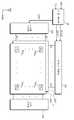
도 3 및 도 4에 도시된 것과 같이, 상기 제1 표시기판(DS1)은 제1 베이스 기판(SUB1), 상기 제1 베이스 기판(SUB1) 상에 배치된 복수 개의 절연층들 및 복수 개의 도전층들을 포함한다. 도 4는 복수 개의 터치센서들 중 하나의 터치센서(TSE)를 도시하였다.3 and 4, the first display substrate DS1 includes a first base substrate SUB1, a plurality of insulating layers disposed on the first base substrate SUB1, . Figure 4 shows one touch sensor (TSE) of a plurality of touch sensors.
상기 제1 베이스 기판(SUB1)의 하면에 상기 터치센서(TSE)가 배치된다. 상기 터치센서(TSE)는 반사율이 낮은 금속 또는 ITO(Indium Tin Oxide), Zno(Zinc Oxide)와 같은 투명한 금속 산화물 등으로 구성될 수 있다. 상기 반사율이 낮은 금속은 크롬 산화물(Chromium oxide), 크롬 질화물(Chromium nitride), 티타늄 산화물(Titanium oxide), 및 티타늄 질화물(Titanium nitride) 중 어느 하나 또는 이들의 합금 등을 포함할 수 있다.The touch sensor TSE is disposed on a lower surface of the first base substrate SUB1. The touch sensor TSE may be composed of a metal having a low reflectance or a transparent metal oxide such as ITO (Indium Tin Oxide) or Zno (Zinc Oxide). The low reflectance metal may include any one of chromium oxide, chromium nitride, titanium oxide, and titanium nitride, or an alloy thereof.
한편, 상기 제1 베이스 기판(SUB1)의 하면과 상기 터치센서(TSE) 사이에는 절연층이 더 배치될 수 있다. 상기 절연층은 적어도 하나의 유기막 및/또는 적어도 하나의 무기막을 포함할 수 있다.An insulating layer may further be disposed between the lower surface of the first base substrate SUB1 and the touch sensor TSE. The insulating layer may include at least one organic film and / or at least one inorganic film.
상기 터치센서(TSE) 상에 제1 절연층(10)이 배치된다. 상기 제1 절연층(10) 상에 게이트 라인(GLi)과 공통 라인(CLi)이 배치된다. 상기 게이트 라인(GLi)으로부터 상기 박막 트랜지스터(TFT)의 게이트 전극(GE)이 분기된다.A first insulating
상기 제1 절연층(10) 상에 상기 게이트 라인(GLi)과 상기 공통 라인(CLi)을 커버하는 제2 절연층(20)이 배치된다. 상기 제2 절연층(20) 상에 데이터 라인들(DLj, DLj+1)이 배치된다. 상기 제2 절연층(20) 상에 상기 게이트 전극(GE)과 중첩하는 반도체층(AL)이 배치된다. 상기 데이터 라인들(DLj, DLj+1) 중 하나의 데이터 라인(DLj)으로부터 상기 박막 트랜지스터(TFT)의 소오스 전극(SE)이 분기된다. 상기 제2 절연층(20) 상에 상기 소오스 전극(SE)과 이격되어 배치된 드레인 전극(DE)이 배치된다. 상기 소오스 전극(SE)과 상기 드레인 전극(DE)은 상기 반도체층(AL)에 각각 중첩한다.A second insulating
상기 제2 절연층(20) 상에 상기 데이터 라인들(DLj, DLj+1)을 커버하는 제3 절연층(30)이 배치된다. 상기 제3 절연층(30) 상에 공통전극(CE)이 배치된다. 상기 공통전극(CE)은 상기 제2 절연층(20) 및 상기 제3 절연층(30)을 관통하는 제1 콘택홀(CH1)을 통해 상기 공통 라인(CLi)에 연결된다.A third insulating
상기 제3 절연층(30) 상에 상기 공통전극(CE)을 커버하는 제4 절연층(40)이 배치된다. 상기 제4 절연층 상에 상기 공통전극(CE)에 중첩하는 상기 화소전극(PE)이 배치된다. 상기 화소전극(PE)은 상기 제3 절연층(30) 및 상기 제4 절연층(40)을 관통하는 제2 콘택홀(CH2)을 통해 상기 드레인 전극(DE)에 연결된다. 상기 제4 절연층(40) 상에는 상기 화소전극(PE)을 보호하는 보호층(미도시) 및 배향막(미도시)이 더 배치될 수 있다.A fourth insulating layer (40) covering the common electrode (CE) is disposed on the third insulating layer (30). And the pixel electrode PE overlapping the common electrode CE is disposed on the fourth insulating layer. The pixel electrode PE is connected to the drain electrode DE through a second contact hole CH2 passing through the third insulating
상기 화소전극(PE)은 복수 개의 슬릿들(SLT)을 포함한다. 상기 화소전극(PE)은 제1 가로부(P1), 상기 제1 가로부(P1)와 이격되어 배치된 제2 가로부(P2), 및 상기 제1 가로부(P1)와 상기 제2 가로부(P2)를 연결하는 복수 개의 세로부들(P3)을 포함할 수 있다. 한편, 상기 화소전극(PE)의 형상은 이에 제한되지 않고, 복수 개의 절개부들을 포함할 수도 있다.The pixel electrode PE includes a plurality of slits SLT. The pixel electrode PE includes a first lateral portion P1, a second lateral portion P2 spaced apart from the first lateral portion P1, and a second lateral portion P2 spaced apart from the first lateral portion P1 and the second lateral portion P1. And a plurality of vertical portions P3 connecting the portions P2. Meanwhile, the shape of the pixel electrode PE is not limited to this, and may include a plurality of cut-out portions.
상기 박막 트랜지스터(TFT)는 상기 게이트 라인(GLi)에 인가된 게이트 신호에 응답하여 상기 데이터 라인(DLj)에 인가된 데이터 전압을 출력한다. 상기 공통전극(CE)은 기준전압을 수신하고, 상기 화소전극(PE)은 상기 데이터 전압에 대응하는 화소전압을 수신한다. 상기 화소전압과 상기 기준전압은 서로 다른 레벨을 갖는다. 상기 공통전극(CE)과 상기 화소전극(PE)은 횡전계를 형성한다. 상기 횡전계에 의해 상기 액정층(LCL)에 포함된 방향자들의 배열이 변화된다.The thin film transistor TFT outputs a data voltage applied to the data line DLj in response to a gate signal applied to the gate line GLi. The common electrode CE receives a reference voltage, and the pixel electrode PE receives a pixel voltage corresponding to the data voltage. The pixel voltage and the reference voltage have different levels. The common electrode CE and the pixel electrode PE form a transverse electric field. The arrangement of the directors included in the liquid crystal layer (LCL) is changed by the transverse electric field.
한편, 다른 실시예에서 상기 공통전극(CE)과 상기 화소전극(PE)은 동일한 층 상에 배치될 수 있다. 또 다른 실시예에서 상기 공통전극(CE)은 상기 제2 표시기판(DS2) 상에 배치될 수 있고, 이때 상기 공통전극들(CE)과 상기 화소전극들(PE)은 수직전계를 형성한다.Meanwhile, in another embodiment, the common electrode CE and the pixel electrode PE may be disposed on the same layer. In yet another embodiment, the common electrode CE may be disposed on the second display substrate DS2, wherein the common electrodes CE and the pixel electrodes PE form a vertical electric field.
상기 제2 표시기판(DS2)은 제2 베이스 기판(SUB2), 차광층(BM), 컬러필터(CF)를 포함한다. 상기 차광층(BM)은 개구부(BM-OP)를 포함한다. 상기 컬러필터(CF)는 상기 개구부(BM-OP)에 중첩하게 배치된다. 실질적으로 상기 화소영역(PXA)은 상기 개구부(BM-OP)에 대응하고, 상기 차광영역(LSA)은 상기 차광층(BM)이 배치된 영역에 대응한다. 도 3 및 도 4는 하나의 화소영역(PXA)을 기준으로 도시하였으나, 상기 차광층(BM)은 도 2에 도시된 화소영역들(PXA)에 대응하는 개구부들을 포함한다.The second display substrate DS2 includes a second base substrate SUB2, a light-shielding layer BM, and a color filter CF. The light-shielding layer BM includes an opening (BM-OP). The color filter CF is arranged to overlap the opening BM-OP. Substantially the pixel region PXA corresponds to the opening portion BM-OP and the light shielding region LSA corresponds to a region where the light shielding layer BM is disposed. Although FIGS. 3 and 4 show one pixel region PXA as a reference, the light blocking layer BM includes openings corresponding to the pixel regions PXA shown in FIG.
또한, 상기 복수 개의 개구부들(BM-OP)에 중첩하게 복수 개의 컬러필터들(CF)이 배치될 수 있다. 상기 복수 개의 컬러필터들(CF)은 서로 다른 컬러를 갖는 컬러필터들을 포함할 수 있다. 예컨대, 상기 복수 개의 컬러필터들(CF) 중 일부는 레드, 다른 일부는 그린, 또 다른 일부는 블루 컬러를 가질 수 있다.In addition, a plurality of color filters CF may be disposed to overlap the plurality of openings BM-OP. The plurality of color filters CF may include color filters having different colors. For example, some of the plurality of color filters CF may have red, others may be green, and some may have blue color.
한편, 다른 실시예에서 상기 차광층(BM)과 상기 컬러필터(CF)는 상기 제1 베이스 기판(SUB1) 상에 배치될 수 있다. 예컨대, 상기 차광층(BM)과 상기 컬러필터(CF)는 상기 제1 절연층(10)을 대체할 수 있다.Meanwhile, in another embodiment, the light-shielding layer BM and the color filter CF may be disposed on the first base substrate SUB1. For example, the light-shielding layer BM and the color filter CF may replace the first insulating
도 5를 참조하여 터치 이벤트를 감지하는 상기 터치센서(TSE)의 동작원리를 설명한다. 상기 게이트 라인(GLi) 및 상기 게이트 전극(GE)에 전원전압(Pv)이 인가된다. 상기 전원전압(Pv)은 게이트 전압이다. 제1 저항(RGL)은 상기 게이트 라인(GLi)의 내부저항이고, 제2 저항(RTSE)은 상기 터치센서(TSE)의 내부저항이며, 제3 저항(RRD)은 상기 표시패널(DP)에 구비된 기타저항이다.The operation principle of the touch sensor TSE for sensing a touch event will be described with reference to FIG. The power source voltage Pv is applied to the gate line GLi and the gate electrode GE. The power supply voltage Pv is a gate voltage. The first resistor RGL is an internal resistance of the gate line GLi and the second resistor RTSE is an internal resistance of the touch sensor TSE and the third resistor RRD is an internal resistance of the display panel DP).
상기 게이트 라인(GLi)에 상기 게이트 전압이 인가됨에 따라 상기 터치센서(TSE)와 정전결합된다. 다시 말해, 상기 게이트 라인(GLi)과 상기 터치센서(TSE)는 커패시터(CGT)를 형성한다. 이때, 상기 게이트 라인(GLi)과 상기 공통전극(CE)은 제1 기생커패시터(CTC)를 형성하고, 상기 게이트 라인(GLi)과 상기 드레인 전극(DE) 및 상기 소오스 전극(SE)은 제2 기생커패시터(CTDS)를 형성한다.And is electrostatically coupled to the touch sensor TSE as the gate voltage is applied to the gate line GLi. In other words, the gate line GLi and the touch sensor TSE form a capacitor CGT . The gate line GLi and the common electrode CE form a first parasitic capacitor CTC and the gate line GLi and the drain electrode DE and the source electrode SE form a first parasitic capacitor CTC . To form a dual parasitic capacitor (CTDS ).
상기 제1 베이스 기판(SUB1) 상에 입력수단이 배치되면, 즉 터치이벤트가 발생하면, 상기 게이트 라인(GLi)과 상기 입력수단은 가변커패시터(CTI)를 형성한다. 그에 따라 상기 터치센서(TSE)의 전위는 낮아진다. 상기 터치 감지부(400)는 상기 터치 이벤트가 발생함에 따라 나타나는 상기 터치센서(TSE)의 전위 변화를 검출한다.When the input means is disposed on the first base substrate (SUB1), that is, when a touch event occurs, the gate line (GLi) and the input means form a variable capacitor (CTI). Whereby the potential of the touch sensor TSE is lowered. The
이러한 측면에서 상기 게이트 라인(GLi) 및 상기 게이트 전극(GE)은 터치패널의 입력 터치전극을 이루고, 상기 터치센서(TSE)는 상기 터치패널의 출력 터치전극을 이룬다. 상기 게이트 전압은 상기 터치패널의 감지신호로 이용된다.In this regard, the gate line GLi and the gate electrode GE form an input touch electrode of a touch panel, and the touch sensor TSE forms an output touch electrode of the touch panel. The gate voltage is used as a sensing signal of the touch panel.
도 1 및 도 6을 참조하면, 상기 신호 제어부(100)는 입력 영상신호들(RGB)을 수신하고, 상기 입력 영상신호들(RGB)을 상기 표시패널(DP)의 동작모드에 부합하는 영상데이터들(R'G'B')로 변환한다. 또한, 신호 제어부(100)는 각종 제어신호(CS), 예를 들면 수직동기신호(Vsync), 수평동기신호(Hsync), 메인 클럭신호, 데이터 인에이블신호 등을 입력받고, 제1 및 제2 제어신호들(CONT1, CONT2)을 출력한다.1 and 6, the
상기 게이트 구동부(200)는 상기 제1 제어신호(CONT1)에 응답하여 상기 복수 개의 게이트 라인들(GL1~GLn)에 게이트 신호들을 출력한다. 상기 제1 제어신호(CONT1)는 상기 게이트 구동부(200)의 동작을 개시하는 수직개시신호, 게이트 전압의 출력 시기를 결정하는 게이트 클럭신호 및 게이트 전압의 온 펄스폭을 결정하는 출력 인에이블 신호 등을 포함한다.The
상기 데이터 구동부(300)는 상기 제2 제어신호(CONT2) 및 상기 영상데이터들(R'G'B')을 수신한다. 상기 데이터 구동부(300)는 상기 영상데이터들(R'G'B')을 데이터 전압들(VRGB)로 변환하여 상기 데이터 라인들(DL1~DLm)에 제공한다.The
상기 제2 제어신호(CONT2)는 상기 데이터 구동부(300)의 동작을 개시하는 수평개시신호, 상기 데이터 전압들(VRGB)의 극성을 반전시키는 반전신호 및 상기 데이터 구동부(300)로부터 상기 데이터 전압들(VRGB)이 출력되는 시기를 결정하는 출력지시신호, 상기 데이터 전압들(VRGB)의 온/오프를 제어하는 데이터 인에이블 신호를 포함한다. 상기 데이터 인에이블 신호는 실질적으로 표시구간(DSP)과 비표시구간(BP)을 정의하는 신호이다.The second control signal CONT2 includes a horizontal start signal for starting the operation of the
상기 터치 감지부(400)는 상기 터치센서들로부터 제공된 출력신호들을 수신한다. 상기 터치 감지부(400)는 상기 출력신호들에 근거하여 상기 터치 이벤트가 발생한 지점의 좌표정보를 산출한다.The
예컨대, 상기 터치 감지부(400)는 상기 출력신호들을 수신하는 신호처리부들 및 멀티플랙서부 및 비교부를 포함할 수 있다. 상기 신호처리부들은 상기 터치센서들에 일대일 대응하게 구비될 수 있다.For example, the
상기 신호처리부들 각각은 증폭기, 노이즈 필터, 아날로그-디지털 컨버터 등을 포함한다. 상기 증폭기는 대응하는 출력신호를 증폭시킨다. 상기 노이즈 필터는 상기 증폭된 출력신호의 노이즈를 제거한다. 상기 아날로그-디지털 컨버터는 상기 노이즈가 제거된 출력신호를 디지털 신호로 변환한다.Each of the signal processing units includes an amplifier, a noise filter, an analog-to-digital converter, and the like. The amplifier amplifies the corresponding output signal. The noise filter removes noise of the amplified output signal. The analog-to-digital converter converts the noise-free output signal into a digital signal.
상기 멀티플랙서부는 상기 신호처리부들로부터 수신한 상기 디지털 신호들을 상기 비교부에 제공한다. 상기 비교부는 상기 디지털 신호들을 기준값에 비교하여 상기 터치센서들 중 상기 터치 이벤트가 발생한 지점상에 배치된 터치센서를 검출한다.The multiplexer section provides the digital signals received from the signal processing sections to the comparison section. The comparison unit compares the digital signals with a reference value to detect a touch sensor disposed on a point where the touch event occurred.
도 6에 도시된 것과 같이, 상기 수직동기신호(Vsync)는 복수 개의 프레임 구간들(FRn-1, FRn, FRn+1)을 정의한다. 상기 복수 개의 프레임 구간들(FRn-1, FRn, FRn+1)은 상기 표시구간(DSP)과 상기 비표시구간(BP)을 포함한다. 한편, 상기 비표시구간(BP)은 생략될 수 있다. 상기 수평동기신호(Hsync)는 상기 데이터 구동부(300)에서 상기 데이터 전압들(VRGB)이 출력되는 복수 개의 수평구간들을 정의한다.As shown in FIG. 6, the vertical synchronization signal Vsync defines a plurality of frame periods FRn-1, FRn, and FRn + 1. The plurality of frame periods FRn-1, FRn, and FRn + 1 include the display period DSP and the non-display period BP. On the other hand, the non-display period BP may be omitted. The horizontal synchronization signal Hsync defines a plurality of horizontal intervals in which the data voltages VRGB are output from the
상기 각각의 복수 개의 프레임 구간들(FRn-1, FRn, FRn+1) 동안 게이트 신호들(GSS1~GSSn)은 상기 게이트 라인들(GL1~GLn)에 순차적으로 인가된다. 상기 게이트 신호들(GSS1~GSSn)은 활성화 구간이 서로 다른 펄스신호들이다. 각각의 활성화 구간에서 상기 게이트 신호들(GSS1~GSSn)은 동일한 레벨을 갖는다.Gate signals GSS1 to GSSn are sequentially applied to the gate lines GL1 to GLn during each of the plurality of frame periods FRn-1, FRn, and FRn + 1. The gate signals GSS1 to GSSn are pulse signals having different activation periods. In each activation period, the gate signals GSS1 to GSSn have the same level.
상기 게이트 신호들(GSS1~GSSn)에 의해 상기 터치 감지부(400)에 인가되는 출력신호들이 형성된다. 이하, 상기 게이트 라인들(GL1~GLn), 상기 게이트 신호들(GSS1~GSSn), 상기 터치센서들, 및 상기 출력신호들에 대해 좀 더 상세히 검토한다.Output signals applied to the
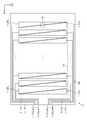
도 7은 도 1에 도시된 표시패널의 평면도이다. 도 8a 및 도 8b는 도 7의 AA영역에 대응하는 평면도이다. 도 7은 상기 제1 베이스 기판(SUB1: 도 4 참조)의 하면에 배치된 복수 개의 터치센서들(TSE1-1~TSE1-k, TSE2-1~TSE2-k)을 평면상에 투영하였다.7 is a plan view of the display panel shown in Fig. 8A and 8B are plan views corresponding to the AA region of FIG. FIG. 7 shows a plurality of touch sensors TSE1-1 to TSE1-k and TSE2-1 to TSE2-k disposed on the lower surface of the first base substrate SUB1 (see FIG. 4) on a plane.
상기 복수 개의 터치센서들(TSE1-1~TSE1-k, TSE2-1~TSE2-k) 각각은 상기 제2 방향(DR2)으로 연장된 형상이다. 상기 복수 개의 터치센서들(TSE1-1~TSE1-k, TSE2-1~TSE2-k) 각각의 상기 제1 방향(DR1)의 너비는 상기 제2 방향(DR2)으로 갈수록 변경된다. Each of the plurality of touch sensors TSE1-1 to TSE1-k and TSE2-1 to TSE2-k extends in the second direction DR2. The width of the first direction DR1 of each of the plurality of touch sensors TSE1-1 to TSE1-k and TSE2-1 to TSE2-k is changed in the second direction DR2.
상기 복수 개의 터치센서들(TSE1-1~TSE1-k, TSE2-1~TSE2-k)은 평면상에서 상기 표시패널의 일부영역(DA, 이하 표시영역)에 배치된다. 상기 표시영역(DA)은 상기 복수 개의 화소영역들(PXA11~PXAnm: 도 1 참조)을 포함한다.The plurality of touch sensors TSE1-1 to TSE1-k and TSE2-1 to TSE2-k are disposed in a partial area DA of the display panel on a plane. The display area DA includes the plurality of pixel areas PXA11 to PXAnm (see FIG. 1).
상기 표시영역(DA)에 인접하게 비표시영역(NDA)이 정의된다. 상기 비표시영역(NDA)은 상기 차광층(BM: 도 4 참조)에 중첩하는 영역이다. 상기 비표시영역(NDA)에 연결라인들(RL1-1~RL1-k, RL2-1~RL2-k)이 배치된다.A non-display area NDA is defined adjacent to the display area DA. The non-display area NDA is a region overlapping the light shielding layer (BM: see Fig. 4). The connection lines RL1-1 to RL1-k and RL2-1 to RL2-k are arranged in the non-display area NDA.
상기 연결라인들(RL1-1~RL1-k, RL2-1~RL2-k)은 상기 복수 개의 터치센서들(TSE1-1~TSE1-k, TSE2-1~TSE2-k)에 각각 연결된다. 상기 연결라인들(RL1-1~RL1-k, RL2-1~RL2-k)은 상기 복수 개의 터치센서들(TSE1-1~TSE1-k, TSE2-1~TSE2-k)로부터 출력된 상기 출력신호들(TSS1-1~TSS1-k, TSS2-1~TSS2-k)을 상기 터치 감지부(400: 도 1 참조)에 제공한다.The connection lines RL1-1 to RL1-k and RL2-1 to RL2-k are connected to the plurality of touch sensors TSE1-1 to TSE1-k and TSE2-1 to TSE2-k, respectively. The connection lines RL1-1 to RL1-k and RL2-1 to RL2-k are connected to the outputs of the plurality of touch sensors TSE1-1 to TSE1-k and TSE2-1 to TSE2- (TSS1-1 to TSS1-k, TSS2-1 to TSS2-k) to the touch sensing unit 400 (see FIG. 1).
상기 복수 개의 터치센서들(TSE1-1~TSE1-k, TSE2-1~TSE2-k)은 형상이 다른 제1 터치센서들(TSE1-1~TSE1-k)과 제2 터치센서들(TSE2-1~TSE2-k)을 포함한다. 상기 제1 터치센서들(TSE1-1~TSE1-k)의 상기 제1 방향(DR1)의 너비는 상기 제2 방향(DR2)으로 갈수록 감소한다. 상기 제2 터치센서들(TSE2-1~TSE2-k)의 제1 방향(DR1)의 너비는 상기 제2 방향(DR2)으로 갈수록 증가한다.The plurality of touch sensors TSE1-1 to TSE1-k and TSE2-1 to TSE2-k are connected to the first touch sensors TSE1-1 to TSE1-k and the second touch sensors TSE2- 1 to TSE2-k). The width of the first touch sensors TSE1-1 through TSE1-k in the first direction DR1 decreases in the second direction DR2. The width of the first direction DR1 of the second touch sensors TSE2-1 through TSE2-k increases as the distance d2 increases in the second direction DR2.
도 7에 도시된 것과 같이, 상기 제1 터치센서들(TSE1-1~TSE1-k)과 상기 제2 터치센서들(TSE2-1~TSE2-k)은 교번하게 배치된다. 상기 제1 터치센서들(TSE1-1~TSE1-k) 각각은 직각 삼각형상일 수 있다. 상기 제2 터치센서들(TSE2-1~TSE2-k)은 상기 제1 터치센서들(TSE1-1~TSE1-k)을 180도 회전시킨 직각 삼각형상이다. 상기 제1 터치센서들(TSE1-1~TSE1-k)과 상기 제2 터치센서들(TSE2-1~TSE2-k) 중 인접한 제1 터치센서와 제2 터치센서는 빗변이 마주하게 배치된다.As shown in FIG. 7, the first touch sensors TSE1-1 through TSE1-k and the second touch sensors TSE2-1 through TSE2-k are alternately arranged. Each of the first touch sensors TSE1-1 to TSE1-k may be a right triangle. The second touch sensors TSE2-1 through TSE2-k are rectangular triangles obtained by rotating the first touch sensors TSE1-1 through TSE1-k by 180 degrees. The first touch sensor and the second touch sensor adjacent to each other among the first touch sensors TSE1-1 through TSE1-k and the second touch sensors TSE2-1 through TSE2-k face each other with a hypotenuse.
도 8a에 도시된 것과 같이, 상기 제1 터치센서(TSE1-1) 및 상기 제2 터치센서(TSE2-1)는 상기 복수 개의 화소영역들(PXA11~PXAnm: 도 1 참조) 중 대응하는 화소영역들(PXA)에 각각 중첩한다. 상기 대응하는 화소영역들(PXA)을 통해 광이 통과하도록 상기 제1 터치센서(TSE1-1) 및 상기 제2 터치센서(TSE2-1)는 투명한 금속 산화물로 구성될 수 있다.As shown in FIG. 8A, the first touch sensor TSE1-1 and the second touch sensor TSE2-1 correspond to the corresponding one of the plurality of pixel regions PXA11 to PXAnm (see FIG. 1) And overlap each other in the pixel regions PXA. The first touch sensor TSE1-1 and the second touch sensor TSE2-1 may be made of a transparent metal oxide such that light passes through the corresponding pixel areas PXA.
도 8b에 도시된 것과 같이, 상기 제1 터치센서(TSE1-1) 및 상기 제2 터치센서(TSE2-1)는 상기 대응하는 화소영역들(PXA)에 인접한 차광영역(LSA)의 일부분에 중첩한다. 상기 제1 터치센서(TSE1-1) 및 상기 제2 터치센서(TSE2-1)는 상기 제1 방향(DR1)으로 연장된 복수 개의 가로부분들(TSE-L)과 상기 제2 방향(DR2)으로 연장된 복수 개의 세로부분들(TSE-C)을 포함한다.8B, the first touch sensor TSE1-1 and the second touch sensor TSE2-1 overlap a part of the light shielding area LSA adjacent to the corresponding pixel areas PXA, do. The first touch sensor TSE1-1 and the second touch sensor TSE2-1 have a plurality of transverse portions TSE-L extending in the first direction DR1 and a plurality of transverse portions TSE- And a plurality of longitudinal portions TSE-C extending to the longitudinal sides.
상기 복수 개의 가로부분들(TSE-L)과 상기 복수 개의 세로부분들(TSE-C)은 서로 연결되어 복수 개의 개구부들(TSE-OP)을 형성한다. 다시 말해, 상기 제1 터치센서(TSE1-1) 및 상기 제2 터치센서(TSE2-1) 각각은 상기 복수 개의 개구부들(TSE-OP)을 구비한 메쉬형상을 갖는다. 이때, 상기 제1 터치센서(TSE1-1) 및 상기 제2 터치센서(TSE2-1) 각각은 반사율이 낮은 금속으로 구성될 수 있다.The plurality of lateral portions TSE-L and the plurality of longitudinal portions TSE-C are connected to each other to form a plurality of openings TSE-OP. In other words, each of the first touch sensor TSE1-1 and the second touch sensor TSE2-1 has a mesh shape having the plurality of openings TSE-OP. At this time, each of the first touch sensor TSE1-1 and the second touch sensor TSE2-1 may be formed of a metal having low reflectance.
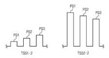
도 9는 도 7에 도시된 제1 터치센서 및 제2 터치센서와 게이트 라인들을 도시한 평면도이다. 도 10은 게이트 신호들과 터치센서들에서 출력되는 출력신호들의 관계를 도시한 타이밍도이다. 도 11a 내지 도 11c는 좌표정보를 산출하는데 이용되는 펄스들을 도시한 도면이다.9 is a plan view showing the first touch sensor, the second touch sensor and the gate lines shown in FIG. 10 is a timing chart showing the relationship between gate signals and output signals output from the touch sensors. 11A to 11C are diagrams showing pulses used to calculate coordinate information.
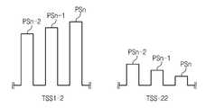
도 9는 상기 제1 터치센서들(TSE1-1~TSE1-k: 도 7 참조)과 상기 제2 터치센서들(TSE2-1~TSE2-k: 도 7 참조) 중 두 번째 배치된 제1 터치센서(TSE1-2)와 제2 터치센서(TSE2-2)를 도시하였다. 또한, 도 9는 상기 제2 방향(DR2)의 좌표정보가 다른 제1 내지 제3 터치지점들(TPP1, TPP2, TPP3)을 도시하였다.FIG. 9 is a diagram showing a relationship between the first touch sensors TSE1-1 through TSE1-k (see FIG. 7) and the second touches arranged second among the second touch sensors TSE2-1 through TSE2-k The sensors TSE1-2 and the second touch sensor TSE2-2 are shown. 9 shows the first to third touch points TPP1, TPP2 and TPP3 having different coordinate information in the second direction DR2.
상기 게이트 라인들(GL1~GLn)에 게이트 신호들(GSS1~GSSn)이 순차적으로 인가됨에 따라 상기 게이트 라인들(GL1~GLn)과 상기 제1 터치센서(TSE1-2)는 커패시터(CGT:도 5참조)를 형성한다. 상기 제2 터치센서(TSE2-2) 역시 상기 게이트 라인들(GL1~GLn)과 커패시터(CGT)를 형성한다.As the gate signals GSS1 to GSSn are sequentially applied to the gate lines GL1 to GLn, the gate lines GL1 to GLn and the first touch sensor TSE1-2 are connected to the capacitor CGT, 5). The second touch sensor TSE2-2 also forms the gate lines GL1 to GLn and the capacitor CGT .
도 10에 도시된 것과 같이, 상기 제1 터치센서(TSE1-2) 및 상기 제2 터치센서(TSE2-2)는 제1 출력신호(TSS1-2) 및 제2 출력신호(TSS2-2)를 각각 출력한다. 상기 제1 출력신호(TSS1-2) 및 상기 제2 출력신호(TSS2-2) 각각은 복수 개의 펄스들을 포함한다. 상기 복수 개의 펄스들은 상기 게이트 신호들(GSS1~GSSn)에 근거하여 생성된다.As shown in FIG. 10, the first touch sensor TSE1-2 and the second touch sensor TSE2-2 output the first output signal TSS1-2 and the second output signal TSS2-2 Respectively. Each of the first output signal TSS1-2 and the second output signal TSS2-2 includes a plurality of pulses. The plurality of pulses are generated based on the gate signals GSS1 to GSSn.
상기 제1 출력신호(TSS1-2) 및 상기 제2 출력신호(TSS2-2) 각각의 상기 복수 개의 펄스들의 레벨은 상기 게이트 라인들(GL1~GLn)과 상기 제1 터치센서(TSE1-2) 또는 상기 제2 터치센서(TSE2-2)의 중첩면적에 따라 결정된다. 상기 게이트 라인들(GL1~GLn)은 후순위로 갈수록 상기 제1 터치센서(TSE1-2)에 중첩하는 면적이 증가된다. 따라서, 상기 게이트 라인들(GL1~GLn)과 상기 제1 터치센서(TSE1-2)가 이루는 커패시터(CGT)에 충전된 전하량은 후순위로 갈수록 증가되고, 상기 제1 출력신호(TSS1-2)의 복수 개의 펄스들의 레벨은 후순위로 갈수록 증가된다.The level of the plurality of pulses of the first output signal TSS1-2 and the second output signal TSS2-2 is controlled by the gate lines GL1 to GLn and the first touch sensor TSE1-2, Or the overlap area of the second touch sensor TSE2-2. The area of the gate lines GL1 to GLn overlapping with the first touch sensor TSE1-2 increases as the position of the gate lines GL1 to GLn decreases. Therefore, the amount of charge charged in the capacitor CGT formed by the gate lines GL1 to GLn and the first touch sensor TSE1-2 increases as the subordinate order increases, and the first output signal TSS1-2, The level of the plurality of pulses of the pulse signal is increased toward the subordinate.
그에 반하여 상기 게이트 라인들(GL1~GLn)은 후순위로 갈수록 상기 제2 터치센서(TSE2-2)에 중첩하는 면적이 감소된다. 따라서, 상기 제2 출력신호(TSS2-2)의 복수 개의 펄스들의 레벨은 후순위로 갈수록 감소된다.On the other hand, the area of the gate lines GL1 to GLn overlapping with the second touch sensor TSE2-2 decreases as the position of the gate lines GL1 to GLn decreases. Therefore, the level of the plurality of pulses of the second output signal TSS2-2 decreases as it goes to the subordinate.
상기 터치 감지부(400: 도 1 참조)는 상기 표시구간(DSP) 동안 터치 이벤트가 발생하였는지 여부를 복수 측정할 수 있다. 상기 터치 감지부(400)는 상기 제1 출력신호(TSS1-2)의 상기 복수 개의 펄스들 중 일부의 펄스들 또는 상기 제2 출력신호(TSS2-2)의 상기 복수 개의 펄스들 중 일부의 펄스들만으로 터치 이벤트가 발생하였는지 여부를 측정할 수 있다.The touch sensing unit 400 (see FIG. 1) may measure a plurality of touch events during the display period (DSP). The
도 11a는 첫번째 게이트 라인 내지 세번째 게이트 라인(GL1~GL3: 도 9 참조)에 인가된 게이트 신호들(GSS1~GSS3, 이하 제1 내지 제3 게이트 신호들)에 의해 생성된 상기 제1 출력신호(TSS1-2) 및 상기 제2 출력신호(TSS1-2)를 도시하였다.11A shows the first output signal (FIG. 11A) generated by the gate signals (GSS1 to GSS3, hereinafter referred to as first to third gate signals) applied to the first to third gate lines GL1 to GL3 TSS1-2 and the second output signal TSS1-2.
상기 터치 이벤트가 발생하면, 상기 제1 터치센서(TSE1-2) 및/또는 상기 제2 터치센서(TSE2-2)과 상기 입력수단 사이에 의해 생성된 상기 가변커패시터(CTI:도 5참조)에 따라 상기 제1 내지 제3 게이트 신호들(GSS1~GSS3)에 의해 생성된 펄스들(PS1~PS3)의 레벨은 변경된다. 상기 터치 감지부(400)는 상기 펄스들(PS1~PS3)의 레벨 변화를 측정하여 상기 제1 내지 제3 게이트 신호들(GSS1~GSS3)이 활성화되는 시점에서 발생한 터치 이벤트를 검출한다.When an event occurs, the touch, the first touch sensor (TSE1-2) and / or the second touch sensor (TSE2-2) and the variable capacitor that is generated by means between the input(TI C: see FIG. 5) The levels of the pulses PS1 to PS3 generated by the first to third gate signals GSS1 to GSS3 are changed. The
한편, 상기 펄스들(PS1~PS3)의 레벨 변화량은 상기 제1 내지 제3 터치지점(TPP1, TPP2, TPP3)에 따라 다르다. 이에 대한 상세한 설명은 도 12a 내지 도 12b를 참조하여 후술한다.On the other hand, the amount of level change of the pulses PS1 to PS3 varies depending on the first to third touch points TPP1, TPP2 and TPP3. A detailed description thereof will be described later with reference to Figs. 12A to 12B.
도 11b는 i-1번째 내지 i+1번째 게이트 라인(GLi-1~GLi+1: 도 9 참조)에 인가된 게이트 신호들(GSSi-1~GSSi+1, 이하 i-1번째 내지 i+1번째 게이트 신호들)에 의해 생성된 상기 제1 출력신호(TSS1-2) 및 상기 제2 출력신호(TSS1-2)를 도시하였다. 도 11c는 n-2번째 내지 n번째 게이트 라인(GLin-2~GLn: 도 9 참조)에 인가된 게이트 신호들(GSSn-2~GSSn, 이하 n-2번째 내지 n번째 게이트 신호들)에 의해 생성된 상기 제1 출력신호(TSS1-2) 및 상기 제2 출력신호(TSS1-2)를 도시하였다.11B shows gate signals (GSSi-1 to
상기 터치 감지부(400)는 상기 i-1번째 내지 i+1번째 게이트 신호들(GSSi-1~GSSi+1)로부터 생성된 펄스들 또는 n-2번째 내지 n번째 게이트 신호들(GSSn-2~GSSn)로부터 생성된 펄스들을 이용하여 각각의 활성화 시점에서 발생한 터치 이벤트를 검출할 수 있다. 결과적으로, 상기 터치 감지부(400)는 상기 표시구간(DSP)에 생성된 상기 제1 출력신호(TSS1-2) 및/또는 상기 제2 출력신호(TSS1-2)의 복수 개의 펄스들 중 3개의 펄스 단위로 터치 이벤트 발생 여부를 측정할 수 있다. 따라서, 상기 표시구간(DSP) 동안에 복수 회의 터치 이벤트가 발생하더라고, 상기 복수 회의 터치 이벤트를 모두 검출할 수 있다.The
한편, 상기 터치 이벤트를 측정하는 주기는 변경될 있다. 예컨대, 상기 터치 이벤트는 5개의 펄스 단위로 측정되거나, 상기 표시구간(DSP)마다 1회씩 측정될 수도 있다.Meanwhile, the period for measuring the touch event may be changed. For example, the touch event may be measured in units of five pulses, or may be measured once in each of the display periods (DSP).
이하, 도 12a 내지 도 12c를 참조하여 상기 터치지점의 좌표산출방법에 대해 좀 더 상세히 검토한다. 도 12a 내지 도 12c는 터치지점의 위치에 따라 나타나는 펄스들의 레벨 변화를, 도 11a에 도시된 펄스들을 예시하여 도시하였다. 도 12a 내지 도 12c에 도시된 제1 내지 제3 펄스들(PS1~PS3)의 점선은 터치 이벤트가 발생하였을 때의 레벨을 나타낸다.Hereinafter, a method of calculating coordinates of the touch point will be described in more detail with reference to FIGS. 12A to 12C. Figs. 12A to 12C illustrate the level change of the pulses according to the position of the touch point by exemplifying the pulses shown in Fig. 11A. The dotted lines of the first to third pulses PS1 to PS3 shown in Figs. 12A to 12C indicate the level when the touch event occurs.
상기 제1 터치 센서들(TSE1-1~TSE1-k: 도 7 참조)과 상기 제2 터치 센서들(TSE2-1~TSE2-k: 도 7 참조)에 대한, 상기 레벨이 변경된 출력신호를 출력한 터치센서의 상대적 위치에 근거하여 상기 터치지점의 상기 제1 방향(DR1)의 좌표를 산출한다. 예컨대, 상기 두 번째 배치된 제1 터치센서(TSE1-2)와 제2 터치센서(TSE2-2)로부터 출력된 출력신호의 레벨이 변경되었다면, 상기 제1 터치센서들(TSE1-1~TSE1-k: 도 7 참조)과 상기 제2 터치센서들(TSE2-1~TSE2-k: 도 7 참조)에 대한 상기 두 번째 배치된 제1 터치센서(TSE1-2)와 제2 터치센서(TSE2-2)의 상대적 위치가 상기 터치지점의 제1 방향(DR1)의 좌표정보이다. 한편, 상기 터치지점의 제1 방향(DR1)의 좌표정보는 상기 제1 출력신호(TSS1-2) 및 상기 제2 출력신호(TSS1-2) 중 어느 하나의 신호에만 근거하여 산출될 수도 있다.The output signal of the level changed for the first touch sensors TSE1-1 through TSE1-k (see FIG. 7) and the second touch sensors TSE2-1 through TSE2-k (see FIG. 7) The coordinates of the touch point in the first direction DR1 are calculated based on the relative position of one touch sensor. For example, if the levels of the output signals output from the second touch sensor TSE1-2 and the second touch sensor TSE2-2 are changed, the first touch sensors TSE1-1 to TSE1- the first touch sensor TSE1-2 and the second touch sensor TSE2-2 for the second touch sensors TSE2-1 through TSE2-k (see FIG. 7) 2 is the coordinate information of the first direction DR1 of the touch point. The coordinate information in the first direction DR1 of the touch point may be calculated based on only one of the first output signal TSS1-2 and the second output signal TSS1-2.
상기 터치지점의 제2 방향(DR2)의 좌표정보는 상기 제1 출력신호(TSS1-2) 및/또는 상기 제2 출력신호(TSS1-2)의 상기 펄스들의 레벨 변화량에 근거하여 산출될 수 있다. 도 12a 내지 도 12c를 참조하면 상기 제1 출력신호(TSS1-2) 및 상기 제2 출력신호(TSS1-2) 각각의 펄스들의 레벨 변화량이 서로 다른 것을 알 수 있다.The coordinate information in the second direction DR2 of the touch point may be calculated based on the level change amount of the pulses of the first output signal TSS1-2 and / or the second output signal TSS1-2 . Referring to FIGS. 12A to 12C, it can be seen that the level variations of the pulses of the first output signal TSS1-2 and the second output signal TSS1-2 are different from each other.
도 12a는 제1 터치지점(TPP1: 도 9 참조)에서 터치이벤트가 발생한 것을 가정하였다. 상기 입력수단과 상기 제1 터치센서(TSE1-2)의 중첩면적은 상기 입력수단과 상기 제2 터치센서(TSE2-2)의 중첩면적보다 좁다. 따라서, 상기 제1 출력신호(TSS1-2)의 제1 내지 제3 펄스들(PS1~PS3)의 감소율은 상기 제2 출력신호(TSS2-2)의 제1 내지 제3 펄스들(PS1~PS3)의 감소율보다 적다.12A assumes that a touch event has occurred at the first touch point TPP1 (see FIG. 9). The overlapping area of the input means and the first touch sensor TSE1-2 is narrower than the overlapping area of the input means and the second touch sensor TSE2-2. Accordingly, the rate of decrease of the first to third pulses PS1 to PS3 of the first output signal TSS1-2 is smaller than the rate of decrease of the first to third pulses PS1 to PS3 of the second output signal TSS2-2, ).
도 12b는 제2 터치지점(TPP2: 도 9 참조)에서 터치이벤트가 발생한 것을 가정한 것이고, 도 12c는 제3 터치지점(TPP3: 도 9 참조)에서 터치이벤트가 발생한 것을 가정한 것이다. 상기 입력수단과 상기 제1 터치센서(TSE1-2)의 중첩면적이 증가할수록 상기 제1 출력신호(TSS1-2)의 제1 내지 제3 펄스들(PS1~PS3)의 감소율은 증가한다. 상기 입력수단과 상기 제2 터치센서(TSE2-2)의 중첩면적이 감소할수록 상기 제2 출력신호(TSS2-2)의 제1 내지 제3 펄스들(PS1~PS3)의 감소율은 감소한다.12B shows a case where a touch event occurs at the second touch point TPP2 (see FIG. 9), and FIG. 12C shows a case where a touch event occurs at the third touch point TPP3 (see FIG. 9). As the overlapping area of the input means and the first touch sensor TSE1-2 increases, the rate of decrease of the first through third pulses PS1 through PS3 of the first output signal TSS1-2 increases. The reduction rate of the first to third pulses PS1 to PS3 of the second output signal TSS2-2 decreases as the overlapping area of the input means and the second touch sensor TSE2-2 decreases.
상기 제1 출력신호(TSS1-2) 및 상기 제2 출력신호(TSS2-2) 중 어느 하나의 상기 제1 내지 제3 펄스들(PS1~PS3)의 감소율에 근거하여 상기 터치지점의 상기 제2 방향(DR2)의 좌표정보를 획득할 수 있다. 이러한 산출방법은 도 11b 및 도 11c에 도시된 펄스들에도 동일하게 적용될 수 있다. 또한, 서로 반비례하는 상기 제1 출력신호(TSS1-2)의 펄스들의 감소율과 상기 제2 출력신호(TSS2-2)의 펄스들의 감소율에 근거하여, 다시 말해 상기 제1 출력신호(TSS1-2) 및 상기 제2 출력신호(TSS2-2)를 상호보완하여, 더 정확한 상기 터치지점의 상기 제2 방향(DR2)의 좌표정보를 획득할 수 있다.Wherein the second output signal (TSS1-2) and the second output signal (TSS2-2) are generated based on the rate of decrease of the first to third pulses (PS1 to PS3) It is possible to obtain the coordinate information of the direction DR2. This calculation method can be equally applied to the pulses shown in Figs. 11B and 11C. Based on the reduction rate of the pulses of the first output signal TSS1-2 and the reduction rate of the pulses of the second output signal TSS2-2 inversely proportional to each other, And the second output signal (TSS2-2) to obtain more accurate coordinate information of the touch point in the second direction (DR2).
도 13는 본 발명의 일 실시예에 따른 표시패널의 단면도이다. 이하, 도 13를 참조하여 본 실시예에 따른 표시장치를 설명한다. 다만, 도 1 내지 도 12c를 참조하여 설명한 구성과 동일한 구성에 대한 상세한 설명은 생략한다.13 is a cross-sectional view of a display panel according to an embodiment of the present invention. Hereinafter, a display device according to the present embodiment will be described with reference to FIG. However, the detailed description of the same components as those described with reference to Figs. 1 to 12C will be omitted.
도 13에 도시된 표시장치는 도 4에 도시된 표시장치와 층구조가 일부 상이하다. 게이트 라인(미도시)은 상기 제1 베이스 기판(SUB1)의 하측에 배치되고, 상기 터치센서(TSE)는 상기 제1 베이스 기판(SUB1)의 상측에 배치된다.The display device shown in Fig. 13 is different in layer structure from the display device shown in Fig. A gate line (not shown) is disposed below the first base substrate SUB1, and the touch sensor TSE is disposed above the first base substrate SUB1.
도 13에 도시된 것과 같이, 상기 제1 베이스 기판(SUB1)의 하면에 공통 라인(CLi)과 상기 게이트 라인으로부터 분기된 게이트 전극(GE)이 배치된다. 상기 제1 베이스 기판(SUB1)의 하면 상에 상기 공통 라인(CLi)과 상기 게이트 라인을 커버하는 제1 절연층(10-1)이 배치된다. 상기 제1 절연층(10-1)은 도 4의 제2 절연층(20)에 대응한다.As shown in FIG. 13, a common line CLi and a gate electrode GE branched from the gate line are disposed on the lower surface of the first base substrate SUB1. A first insulating layer 10-1 covering the common line CLi and the gate line is disposed on the lower surface of the first base substrate SUB1. The first insulating layer 10-1 corresponds to the second insulating
상기 터치센서(TSE)는 상기 제1 베이스 기판(SUB1)의 상면에 배치된다. 상기 제1 베이스 기판(SUB1)의 상면에는 상기 터치센서(TSE)를 보호하는 보호판(SS)이 배치된다. 한편, 상기 터치센서(TSE)와 상기 제1 베이스 기판(SUB1)의 상면 사이에는 절연층(미도시)이 더 배치될 수 있다.The touch sensor TSE is disposed on the upper surface of the first base substrate SUB1. A protection plate SS for protecting the touch sensor TSE is disposed on the upper surface of the first base substrate SUB1. An insulating layer (not shown) may be further disposed between the touch sensor TSE and the upper surface of the first base substrate SUB1.
도 14는 본 발명의 일 실시예에 따른 표시패널의 평면도이다. 이하, 도 14을 참조하여 본 실시예에 따른 표시장치를 설명한다. 다만, 도 1 내지 도 13를 참조하여 설명한 구성과 동일한 구성에 대한 상세한 설명은 생략한다.14 is a plan view of a display panel according to an embodiment of the present invention. Hereinafter, a display device according to the present embodiment will be described with reference to FIG. However, the detailed description of the same components as those described with reference to Figs. 1 to 13 will be omitted.
도 14에 도시된 것과 같이, 표시장치(DP-1)에 구비된 복수 개의 터치센서들(TSE)은 복수 개의 그룹들로 구분될 수 있다. 상기 복수 개의 그룹들은 제2 방향(DR2)으로 나열된다. 도 14에는 2개의 그룹들(TSE-G1, TSE-G2)을 예시적으로 도시하였다. 도 14에서 상기 2개의 그룹들(TSE-G1, TSE-G2) 각각의 터치센서들에 연결된 연결라인들은 미도시 되었다.As shown in FIG. 14, the plurality of touch sensors TSE provided in the display device DP-1 may be divided into a plurality of groups. The plurality of groups are arranged in a second direction DR2. 14, two groups (TSE-G1, TSE-G2) are exemplarily shown. In FIG. 14, connection lines connected to the touch sensors of the two groups TSE-G1 and TSE-G2, respectively, are not shown.
상기 2개의 그룹들(TSE-G1, TSE-G2) 각각은 상기 제2 방향(DR2)으로 연장되며, 제1 방향(DR1)으로 나열된 터치센서들(TSE1, TSE2)을 포함한다. 상기 2개의 그룹(TSE-G1, TSE-G2)들 각각의 상기 터치센서들(TSE1, TSE2)은 도 7에 도시된 터치센서들(TSE1-1~TSE1-k, TSE2-1~TSE2-k)과 기능적으로 동일하다.Each of the two groups TSE-G1 and TSE-G2 extends in the second direction DR2 and includes touch sensors TSE1 and TSE2 arranged in a first direction DR1. The touch sensors TSE1 and TSE2 of each of the two groups TSE-G1 and TSE-G2 correspond to the touch sensors TSE1-1 to TSE1-k, TSE2-1 to TSE2-k ).
상기 2개의 그룹들(TSE-G1, TSE-G2) 각각의 터치지점 좌표정보 산출방법은 도 9 내지 도 12c를 참조하여 설명한 것과 동일하다. 다만, 상기 2개의 그룹들(TSE-G1, TSE-G2)은 서로 다른 상기 제2 방향(DR2)의 좌표정보를 갖는다.The touch point coordinate information calculation method of each of the two groups (TSE-G1, TSE-G2) is the same as that described with reference to Figs. 9 to 12C. However, the two groups TSE-G1 and TSE-G2 have coordinate information in the second direction DR2 different from each other.
상기 터치지점의 상기 제2 방향(DR2)의 좌표정보는 레벨이 변화된 출력신호를 출력한 터치센서가 상기 제1 그룹(TSE-G1)과 상기 제2 그룹(TSE-G2) 중 어느 그룹에 속하는지에 따라 1차적으로 산출된 후, 도 9 내지 도 12c를 참조하여 설명한 것과 동일한 방식으로 2차적으로 산출된다.The coordinate information of the touch point in the second direction DR2 may be obtained when the touch sensor outputting the level-changed output signal belongs to any one of the first group TSE-G1 and the second group TSE-G2 And then calculated in the same manner as described with reference to Figs. 9 to 12C.
도 15a 내지 도 15c는 본 발명의 일 실시예에 따른 표시패널의 평면도이다. 이하, 도 15a 내지 도 15c를 참조하여 본 실시예에 따른 표시장치를 설명한다. 다만, 도 1 내지 도 13을 참조하여 설명한 구성과 동일한 구성에 대한 상세한 설명은 생략한다. 도 15a 내지 도 15c에서 터치센서들에 연결된 연결라인들은 미도시 되었다.15A to 15C are plan views of a display panel according to an embodiment of the present invention. Hereinafter, a display device according to the present embodiment will be described with reference to FIGS. 15A to 15C. FIG. However, the detailed description of the same components as those described with reference to Figs. 1 to 13 will be omitted. The connection lines connected to the touch sensors in Figures 15A-15C are not shown.
도 15a에 도시된 것과 같이, 표시장치(DP-2)는 형상이 다른 제1 터치센서들(TSE10-1~TSE10-k)과 제2 터치센서들(TSE20-1~TSE20-k)을 포함한다. 상기 제1 터치센서들(TSE10-1~TSE10-k) 각각은 이등변 삼각형상일 수 있다. 상기 제2 터치센서들(TSE20-1~TSE20-k)은 상기 제1 터치센서들(TSE10-1~TSE10-k)이 180도 회전된 형상일 수 있다. 상기 제1 터치센서들(TSE10-1~TSE10-k)과 상기 제2 터치센서들(TSE20-1~TSE20-k)은 동일한 면적을 갖는다.15A, the display device DP-2 includes first touch sensors TSE10-1 through TSE10-k having different shapes and second touch sensors TSE20-1 through TSE20-k do. Each of the first touch sensors TSE10-1 to TSE10-k may be an isosceles triangle shape. The second touch sensors TSE20-1 through TSE20-k may be formed by rotating the first touch sensors TSE10-1 through TSE10-k by 180 degrees. The first touch sensors TSE10-1 through TSE10-k and the second touch sensors TSE20-1 through TSE20-k have the same area.
상기 제1 터치센서들(TSE10-1~TSE10-k)과 상기 제2 터치센서들(TSE20-1~TSE20-k)은 교번하게 배치된다. 상기 제1 터치센서들(TSE10-1~TSE10-k)의 꼭지점은 상기 제2 터치센서들(TSE20-1~TSE20-k)의 밑변에 인접하고, 상기 제2 터치센서들(TSE20-1~TSE20-k)의 꼭지점은 상기 제1 터치센서들(TSE10-1~TSE10-k)의 밑변에 인접한다.The first touch sensors TSE10-1 through TSE10-k and the second touch sensors TSE20-1 through TSE20-k are alternately arranged. The vertexes of the first touch sensors TSE10-1 to TSE10-k are adjacent to the base of the second touch sensors TSE20-1 to TSE20-k, and the vertices of the second touch sensors TSE20-1 to TSE10- TSE20-k are adjacent to the base of the first touch sensors TSE10-1 to TSE10-k.
상기 표시장치(DP-2)는 제3 터치센서(TSE30)와 제4 터치센서(TSE40)를 더 포함할 수 있다. 상기 제3 터치센서(TSE30)와 상기 제4 터치센서(TSE40)는 상기 표시영역(DA) 중 상기 제1 터치센서들(TSE10-1~TSE10-k)과 상기 제2 터치센서들(TSE20-1~TSE20-k)이 배치되지 않는 영역에 배치된다. 상기 제3 터치센서(TSE30)와 상기 제4 터치센서(TSE40)의 상기 제1 방향(DR1)의 너비는 상기 제2 방향(DR2)으로 갈수록 변경된다.The display device DP-2 may further include a third touch sensor TSE30 and a fourth touch sensor TSE40. The third touch sensor TSE30 and the fourth touch sensor TSE40 are connected to the first touch sensors TSE10-1 through TSE10-k and the second touch sensors TSE20- 1 to TSE20-k) are not disposed. The width of the third touch sensor TSE30 and the fourth touch sensor TSE40 in the first direction DR1 is changed in the second direction DR2.
도 15b에 도시된 것과 같이, 표시장치(DP-3)는 형상이 다른 제1 터치센서들(TSE100-1~TSE100-k)과 제2 터치센서들(TSE200-1~TSE200-k)을 포함한다. 상기 제1 터치센서들(TSE100-1~TSE100-k)과 상기 제2 터치센서들(TSE200-1~TSE200-k)은 교번하게 배치된다.15B, the display device DP-3 includes first touch sensors TSE100-1 to TSE100-k having different shapes and second touch sensors TSE200-1 to TSE200-k do. The first touch sensors TSE100-1 through TSE100-k and the second touch sensors TSE200-1 through TSE200-k are alternately arranged.
상기 제1 터치센서들(TSE100-1~TSE100-k) 각각은 등변 사다리꼴 형상일 수 있다. 상기 제2 터치센서들(TSE200-1~TSE200-k)은 상기 제1 터치센서들(TSE100-1~TSE100-6)이 180도 회전된 형상일 수 있다.Each of the first touch sensors TSE100-1 to TSE100-k may have an isosceles trapezoidal shape. The second touch sensors TSE200-1 to TSE200-k may have a shape in which the first touch sensors TSE100-1 to TSE100-6 are rotated 180 degrees.
도 15c에 도시된 것과 같이, 표시장치(DP-4)는 형상 및 면적이 다른 제1 터치센서들(TSE1000-1~TSE1000-k)과 제2 터치센서들(TSE2000-1~TSE2000-k)을 포함한다.15C, the display device DP-4 includes first touch sensors TSE1000-1 to TSE1000-k and second touch sensors TSE2000-1 to TSE2000-k having different shapes and areas, .
상기 제1 터치센서들(TSE1000-1~TSE1000-k) 및 제2 터치센서들(TSE2000-1~TSE2000-k)은 이등변 삼각형상에서 2개의 등변이 변형된 형상일 수 있다. 상기 제1 터치센서들(TSE1000-1~TSE1000-k)은 1개의 밑변과 볼록한 2개의 등변 및 3개의 꼭지점을 갖는다. 상기 제2 터치센서들(TSE2000-1~TSE2000-k)은 1개의 밑변과 오목한 2개의 등변 및 3개의 꼭지점을 갖는다. 상기 제1 터치센서들(TSE1000-1~TSE1000-k)과 상기 제2 터치센서들(TSE2000-1~TSE2000-k)은 교번하게 배치된다.The first touch sensors TSE1000-1 through TSE1000-k and the second touch sensors TSE2000-1 through TSE2000-k may be two equally deformed shapes on an isosceles triangle. The first touch sensors TSE1000-1 to TSE1000-k have one base and two convex sides and three vertexes. The second touch sensors TSE2000-1 to TSE2000-k have one base, two concave sides, and three vertices. The first touch sensors TSE1000-1 through TSE1000-k and the second touch sensors TSE2000-1 through TSE2000-k are alternately arranged.
상기 표시장치(DP-4)는 상기 표시영역(DA) 중 상기 제1 터치센서들(TSE1000-1~TSE1000-k)과 상기 제2 터치센서들(TSE2000-1~TSE2000-k)이 배치되지 않는 영역에 배치된 제3 터치센서(TSE3000)와 제4 터치센서(TSE4000)를 더 포함할 수 있다. 상기 제3 터치센서(TSE3000) 및 상기 제4 터치센서(TSE4000)는 변형된 직각 삼각형상이다. 상기 제3 터치센서(TSE3000)는 오목한 빗변을 갖고, 상기 제4 터치센서(TSE4000)는 볼록한 빗변을 갖는다.The display device DP-4 may be configured such that the first touch sensors TSE1000-1 to TSE1000-k and the second touch sensors TSE2000-1 to TSE2000-k are disposed in the display area DA (TSE3000) and a fourth touch sensor (TSE4000) disposed in a region where the first touch sensor The third touch sensor TSE3000 and the fourth touch sensor TSE4000 are deformed right triangular. The third touch sensor TSE3000 has a concave hypotenuse, and the fourth touch sensor TSE4000 has a convex hypotenuse.
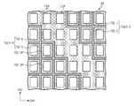
도 16은 본 발명의 일 실시예에 따른 표시패널의 평면도이다. 이하, 도 16를 참조하여 본 실시예에 따른 표시장치를 설명한다. 다만, 도 1 내지 도 13를 참조하여 설명한 구성과 동일한 구성에 대한 상세한 설명은 생략한다.16 is a plan view of a display panel according to an embodiment of the present invention. Hereinafter, a display device according to the present embodiment will be described with reference to FIG. However, the detailed description of the same components as those described with reference to Figs. 1 to 13 will be omitted.
도 16에 도시된 것과 같이, 표시장치(DP-5)는 매트릭스 형태로 배열된 상기 복수 개의 터치 센서들(TSE11~TSEpq)을 포함한다. 상기 복수 개의 터치 센서들(TSE11~TSEpq)은 상기 제1 베이스 기판(SUB1)의 상측 또는 하측에 배치될 수 있다.As shown in Fig. 16, the display device DP-5 includes the plurality of touch sensors TSE11 to TSEpq arranged in a matrix form. The plurality of touch sensors TSE11 to TSEpq may be disposed above or below the first base substrate SUB1.
상기 복수 개의 터치 센서들(TSE11~TSEpq)은 실질적으로 동일한 형상 및 실질적으로 동일한 면적을 갖는다. 상기 복수 개의 터치 센서들(TSE11~TSEpq)은 정사각형 뿐만 아니라, 원형, 다각형등으로 변형될 수 있다.The plurality of touch sensors TSE11 to TSEpq have substantially the same shape and substantially the same area. The plurality of touch sensors TSE11 to TSEpq may be modified into not only a square but also a circle, a polygon, or the like.
도시되지 않았으나, 상기 복수 개의 터치 센서들(TSE11~TSEpq)의 출력신호를 터치 감지부(400)에 제공하는 연결라인들이 배치될 수 있다. 상기 연결라인들은 차광영역(LSA: 도 2 참조)에 중첩하게 배치된다.Although not shown, connection lines for providing output signals of the plurality of touch sensors TSE11 to TSEpq to the
상기 복수 개의 터치 센서들(TSE11~TSEpq)은 상기 게이트 전압이 인가된 상기 게이트 라인들(GL1~GLn)과 정전결합된다. 상기 복수 개의 터치 센서들(TSE11~TSEpq)은 고유의 좌표정보를 갖는다. 따라서, 레벨이 변화된 출력신호를 검출하는 것만으로 터치지점의 좌표정보를 산출할 수 있다.The plurality of touch sensors TSE11 to TSEpq are electrostatically coupled to the gate lines GL1 to GLn to which the gate voltage is applied. The plurality of touch sensors TSE11 to TSEpq have unique coordinate information. Therefore, the coordinate information of the touch point can be calculated only by detecting the output signal whose level is changed.
이상에서는 본 발명의 바람직한 실시예를 참조하여 설명하였지만, 해당 기술 분야의 숙련된 당업자 또는 해당 기술 분야에 통상의 지식을 갖는 자라면, 후술될 특허청구범위에 기재된 본 발명의 사상 및 기술 영역으로부터 벗어나지 않는 범위 내에서 본 발명을 다양하게 수정 및 변경시킬 수 있음을 이해할 수 있을 것이다.While the present invention has been described in connection with what is presently considered to be the most practical and preferred embodiment, it is to be understood that the invention is not limited to the disclosed embodiments, but, on the contrary, It will be understood that various modifications and changes may be made thereto without departing from the scope of the present invention.
따라서, 본 발명의 기술적 범위는 명세서의 상세한 설명에 기재된 내용으로 한정되는 것이 아니라 특허청구범위에 의해 정하여져야만 할 것이다.Therefore, the technical scope of the present invention should not be limited to the contents described in the detailed description of the specification, but should be defined by the claims.
100: 신호 제어부200: 게이트 구동부
300: 데이터 구동부400: 터치 감지부
DP: 표시패널PXA: 화소영역
LSA: 차광영역TSE: 터치센서100: Signal control unit 200: Gate driver
300: Data driver 400: Touch sensing unit
DP: Display panel PXA: Pixel area
LSA: Shading area TSE: Touch sensor
Claims (20)
Translated fromKorean상기 제1 베이스 기판 상에 배치되고, 제1 방향으로 연장되며 상기 제1 방향과 교차하는 제2 방향으로 배열되고, 활성화 구간이 서로 다른 게이트 신호들을 각각 수신하는 복수 개의 게이트 라인들;
상기 복수 개의 화소영역들에 대응하게 배치되며, 상기 게이트 신호들에 응답하여 활성화되는 복수 개의 화소들;
상기 제1 베이스 기판 상에 배치되고, 상기 게이트 신호들을 감지신호들로 이용하여 상기 복수 개의 게이트 라인들과 정전결합되는 복수 개의 터치센서들; 및
상기 복수 개의 터치센서들로부터 제공된 출력신호들로부터 터치지점의 좌표정보를 산출하는 터치 감지부를 포함하는 표시장치.A first base substrate which provides a touch surface and is divided into a light shielding region and a plurality of pixel regions;
A plurality of gate lines arranged on the first base substrate and extending in a first direction and arranged in a second direction intersecting with the first direction, each of the gate lines receiving gate signals having different activation periods;
A plurality of pixels arranged corresponding to the plurality of pixel regions and activated in response to the gate signals;
A plurality of touch sensors disposed on the first base substrate and electrostatically coupled to the plurality of gate lines using the gate signals as sense signals; And
And a touch sensing unit for calculating coordinate information of a touch point from output signals provided from the plurality of touch sensors.
상기 복수 개의 터치센서들은,
상기 제2 방향으로 연장된 형상으로, 상기 제1 방향의 너비는 상기 제2 방향을 따라 변경되는 것을 특징으로 하는 표시장치.The method according to claim 1,
Wherein the plurality of touch sensors include:
And the width of the first direction is changed along the second direction in a shape extending in the second direction.
상기 복수 개의 터치센서들은,
상기 제2 방향을 따라 상기 제1 방향의 너비가 증가되는 제1 터치센서들; 및
상기 제2 방향을 따라 상기 제1 방향의 너비가 감소되는 제2 터치센서들을 포함하는 표시장치.3. The method of claim 2,
Wherein the plurality of touch sensors include:
First touch sensors whose widths in the first direction are increased along the second direction; And
And second touch sensors whose widths in the first direction are decreased along the second direction.
상기 제1 터치센서들 및 상기 제2 터치센서들은 교번하게 배치된 것을 특징으로 하는 표시장치.The method of claim 3,
Wherein the first touch sensors and the second touch sensors are alternately arranged.
상기 출력신호들 각각은 상기 게이트 신호들에 근거하여 생성된 레벨이 다른 복수 개의 펄스들을 포함하는 것을 특징으로 하는 표시장치.3. The method of claim 2,
Wherein each of the output signals includes a plurality of pulses having different levels generated based on the gate signals.
상기 터치 감지부는 상기 복수 개의 펄스들의 변화된 레벨에 근거하여 상기 터치지점의 상기 제2 방향의 좌표정보를 산출하는 것을 특징으로 하는 표시장치.6. The method of claim 5,
Wherein the touch sensing unit calculates coordinate information of the touch point in the second direction based on the changed level of the plurality of pulses.
상기 터치 감지부는 상기 복수 개의 펄스들 중 일부의 펄스들에 근거하여 상기 터치지점의 좌표정보를 산출하는 것을 특징으로 하는 표시장치.6. The method of claim 5,
Wherein the touch sensing unit calculates coordinate information of the touch point based on a part of the pulses among the plurality of pulses.
상기 복수 개의 터치센서들은 복수 개의 그룹들로 구분되고, 상기 복수 개의 그룹들은 상기 제2 방향으로 나열된 것을 특징으로 하는 표시장치.3. The method of claim 2,
Wherein the plurality of touch sensors are divided into a plurality of groups, and the plurality of groups are arranged in the second direction.
상기 복수 개의 게이트 라인들 및 상기 복수 개의 터치센서들은 상기 제1 베이스 기판의 하측에 배치된 것을 특징으로 하는 표시장치.The method according to claim 1,
Wherein the plurality of gate lines and the plurality of touch sensors are disposed on the lower side of the first base substrate.
상기 복수 개의 터치센서들은 상기 제1 베이스 기판의 하면 상에 배치되고,
상기 복수 개의 게이트 라인들은 상기 복수 개의 터치센서들을 커버하는 절연층 상에 배치된 것을 특징으로 하는 표시장치.10. The method of claim 9,
Wherein the plurality of touch sensors are disposed on a lower surface of the first base substrate,
Wherein the plurality of gate lines are disposed on an insulating layer covering the plurality of touch sensors.
상기 복수 개의 게이트 라인들은 상기 제1 베이스 기판의 하측에 배치되고, 상기 복수 개의 터치센서들은 상기 제1 베이스 기판의 상측에 배치된 것을 특징으로 하는 표시장치.The method according to claim 1,
Wherein the plurality of gate lines are disposed on the lower side of the first base substrate, and the plurality of touch sensors are disposed on the upper side of the first base substrate.
상기 제1 베이스 기판 상에 배치되고, 상기 복수 개의 터치센서들에 각각 연결되며, 상기 출력신호들을 상기 터치 감지부에 제공하는 복수 개의 연결라인들을 더 포함하는 표시장치.The method according to claim 1,
Further comprising a plurality of connection lines disposed on the first base substrate and connected to the plurality of touch sensors and providing the output signals to the touch sensing unit.
상기 제1 베이스 기판과 이격되어 배치된 제2 베이스 기판을 더 포함하는 표시장치.The method according to claim 1,
And a second base substrate spaced apart from the first base substrate.
상기 제1 베이스 기판과 상기 제2 베이스 기판 사이에 배치된 액정층을 더 포함하는 표시장치.14. The method of claim 13,
And a liquid crystal layer disposed between the first base substrate and the second base substrate.
상기 제1 베이스 기판 상에 배치되고, 상기 제2 방향으로 연장되며 상기 제1 방향으로 배열되고, 데이터 전압들을 수신하는 복수 개의 데이터 라인들을 더 포함하는 표시장치.15. The method of claim 14,
Further comprising a plurality of data lines arranged on the first base substrate and extending in the second direction and arranged in the first direction and receiving data voltages.
상기 복수 개의 화소들 각각은,
상기 복수 개의 게이트 라인들 중 대응하는 게이트 라인 및 상기 복수 개의 데이터 라인들 중 대응하는 데이터 라인에 연결되고, 상기 대응하는 게이트 라인에 인가된 게이트 신호에 응답하여 상기 대응하는 데이터 라인에 인가된 데이터 신호를 출력하는 박막 트랜지스터;
상기 박막 트랜지스터에 연결되어 상기 데이터 신호에 대응하는 화소전압을 수신하는 화소전극; 및
상기 화소전극과 전계를 형성하는 공통전극을 포함하는 것을 특징으로 하는 표시장치.16. The method of claim 15,
Wherein each of the plurality of pixels comprises:
A data line coupled to a corresponding one of the plurality of gate lines and to a corresponding one of the plurality of data lines, the data signal being applied to the corresponding data line in response to a gate signal applied to the corresponding gate line; A thin film transistor for outputting the thin film transistor;
A pixel electrode connected to the thin film transistor for receiving a pixel voltage corresponding to the data signal; And
And a common electrode which forms an electric field with the pixel electrode.
상기 복수 개의 화소영역들에 중첩하게 상기 제2 베이스 기판 상에 배치된 복수 개의 컬러필터들; 및
상기 차광영역에 중첩하게 상기 제2 베이스 기판 상에 배치된 블랙 매트릭스를 더 포함하는 표시장치.14. The method of claim 13,
A plurality of color filters disposed on the second base substrate to overlap the plurality of pixel regions; And
And a black matrix disposed on the second base substrate so as to overlap the light shielding region.
상기 복수 개의 터치센서들 각각은,
상기 복수 개의 화소영역들 중 일부의 화소영역들에 중첩하는 개구부들을 포함하는 것을 특징으로 하는 표시장치.The method according to claim 1,
Wherein each of the plurality of touch sensors comprises:
Wherein the plurality of pixel regions include openings overlapping the pixel regions of the plurality of pixel regions.
상기 복수 개의 터치센서들은 매트릭스 형태로 배열된 것을 특징으로 하는 표시장치.The method according to claim 1,
Wherein the plurality of touch sensors are arranged in a matrix form.
상기 복수 개의 터치센서들은 실질적으로 동일한 형상 및 실질적으로 동일한 면적을 갖는 것을 특징으로 하는 표시장치.20. The method of claim 19,
Wherein the plurality of touch sensors have substantially the same shape and substantially the same area.
Priority Applications (4)
| Application Number | Priority Date | Filing Date | Title |
|---|---|---|---|
| KR1020130007567AKR20140095152A (en) | 2013-01-23 | 2013-01-23 | Display device |
| CN201310218267.3ACN103941903A (en) | 2013-01-23 | 2013-06-04 | Display device |
| US13/910,919US9423899B2 (en) | 2013-01-23 | 2013-06-05 | Display device |
| JP2013126853AJP2014142908A (en) | 2013-01-23 | 2013-06-17 | Display device |
Applications Claiming Priority (1)
| Application Number | Priority Date | Filing Date | Title |
|---|---|---|---|
| KR1020130007567AKR20140095152A (en) | 2013-01-23 | 2013-01-23 | Display device |
Publications (1)
| Publication Number | Publication Date |
|---|---|
| KR20140095152Atrue KR20140095152A (en) | 2014-08-01 |
Family
ID=51189593
Family Applications (1)
| Application Number | Title | Priority Date | Filing Date |
|---|---|---|---|
| KR1020130007567AWithdrawnKR20140095152A (en) | 2013-01-23 | 2013-01-23 | Display device |
Country Status (4)
| Country | Link |
|---|---|
| US (1) | US9423899B2 (en) |
| JP (1) | JP2014142908A (en) |
| KR (1) | KR20140095152A (en) |
| CN (1) | CN103941903A (en) |
Cited By (1)
| Publication number | Priority date | Publication date | Assignee | Title |
|---|---|---|---|---|
| KR20170051797A (en)* | 2015-10-30 | 2017-05-12 | 엘지디스플레이 주식회사 | Sensor integrated type display device |
Families Citing this family (13)
| Publication number | Priority date | Publication date | Assignee | Title |
|---|---|---|---|---|
| EP3130984B1 (en)* | 2014-04-07 | 2019-09-04 | Murata Manufacturing Co., Ltd. | Touch panel and electronic device |
| KR102218624B1 (en) | 2014-05-26 | 2021-02-23 | 삼성디스플레이 주식회사 | Method of driving display panel and display apparatus for performing the same |
| TWI543054B (en)* | 2014-07-09 | 2016-07-21 | 晨星半導體股份有限公司 | Sensing electrode and sensing capacitance estimation method and apparatus |
| CN104407757A (en) | 2014-12-04 | 2015-03-11 | 深圳市华星光电技术有限公司 | Touch display device |
| KR102301502B1 (en)* | 2015-01-07 | 2021-09-24 | 삼성디스플레이 주식회사 | Touch screen panel comprising touch sensor |
| CN106201126B (en)* | 2015-01-13 | 2019-08-30 | 小米科技有限责任公司 | Touch screen and fingerprint recognition realization device and terminal device |
| KR20160098030A (en) | 2015-01-13 | 2016-08-18 | 시아오미 아이엔씨. | Apparatus for implementing functions of touch screen and fingerprint identification, and terminal device |
| CN104571768B (en) | 2015-01-30 | 2018-03-20 | 京东方科技集团股份有限公司 | A kind of array base palte, In-cell touch panel and display device |
| US10296147B2 (en)* | 2015-02-02 | 2019-05-21 | Samsung Display Co., Ltd. | Touch screen and display device including the same |
| CN115185395A (en)* | 2016-01-20 | 2022-10-14 | 株式会社半导体能源研究所 | Input device, input/output device and data processing device |
| WO2017213175A1 (en)* | 2016-06-09 | 2017-12-14 | シャープ株式会社 | Display device with touch panel and method for manufacturing display device with touch panel |
| US10474295B2 (en) | 2016-11-10 | 2019-11-12 | Samsung Display Co., Ltd. | Display device including sensor and auxiliary sensor parts |
| CN106908977B (en)* | 2017-04-28 | 2020-06-05 | 京东方科技集团股份有限公司 | A touch display substrate, a touch display device and a touch display method |
Family Cites Families (21)
| Publication number | Priority date | Publication date | Assignee | Title |
|---|---|---|---|---|
| KR20010094773A (en) | 2001-03-16 | 2001-11-03 | 장광식 정윤철 | Touch Panel with polarizer and Flat Panel Display with Touch Panel and manufacturing method thereof |
| US20070085838A1 (en) | 2005-10-17 | 2007-04-19 | Ricks Theodore K | Method for making a display with integrated touchscreen |
| US7973771B2 (en)* | 2007-04-12 | 2011-07-05 | 3M Innovative Properties Company | Touch sensor with electrode array |
| JP5295531B2 (en) | 2007-08-27 | 2013-09-18 | 一般財団法人電力中央研究所 | Ultrasonic flaw detection method and apparatus for surface flaw detection |
| JP2009116224A (en) | 2007-11-09 | 2009-05-28 | Seiko Instruments Inc | Touch panel integrated type liquid crystal display device, touch detecting method and portable terminal |
| KR20090059285A (en)* | 2007-12-06 | 2009-06-11 | 삼성전자주식회사 | Display panel |
| JP4816668B2 (en)* | 2008-03-28 | 2011-11-16 | ソニー株式会社 | Display device with touch sensor |
| KR101080183B1 (en)* | 2008-04-04 | 2011-11-07 | (주)멜파스 | Touch sensing apparatus having improved location detection performance for periphery touch |
| KR100994608B1 (en)* | 2008-04-18 | 2010-11-15 | (주)멜파스 | Contact sensing panel comprising an electrode-integrated window, and method of manufacturing the same |
| US20100289755A1 (en) | 2009-05-15 | 2010-11-18 | Honh Kong Applied Science and Technology Research Institute Co., Ltd. | Touch-Sensing Liquid Crystal Display |
| US8415958B2 (en)* | 2009-09-11 | 2013-04-09 | Synaptics Incorporated | Single layer capacitive image sensing |
| KR101588450B1 (en) | 2009-10-23 | 2016-01-25 | 엘지디스플레이 주식회사 | Touch sensor in-cell type organic electroluminescent device and methode of fabricating the same |
| KR101309862B1 (en) | 2009-12-10 | 2013-09-16 | 엘지디스플레이 주식회사 | Liquid Crystal Display Device Including Touch Panel |
| TWI412854B (en) | 2010-02-04 | 2013-10-21 | Chunghwa Picture Tubes Ltd | Touch-sensitive liquid crystal module and integrated touch-sensitive substrate |
| TWI441119B (en)* | 2010-04-02 | 2014-06-11 | Arolltech Co Ltd | Display with in-cell touch sensor |
| KR101691885B1 (en) | 2010-08-16 | 2017-01-02 | 엘지디스플레이 주식회사 | Liquid crystal display device with a built-in touch screen and method for manufacturing the same |
| KR101147085B1 (en) | 2010-08-19 | 2012-05-17 | 금오공과대학교 산학협력단 | Liquid crystal display device having touch sensor embedded therein |
| KR101085089B1 (en) | 2010-09-04 | 2011-11-18 | 이성호 | Capacitive touch detection means, detection method and touch screen panel using level shift, and display device incorporating such capacitive touch screen panel |
| KR101891985B1 (en) | 2010-10-08 | 2018-08-27 | 엘지디스플레이 주식회사 | Liquid crystal display device |
| JP5789113B2 (en)* | 2011-03-31 | 2015-10-07 | 株式会社Joled | Display device and electronic device |
| TWI438666B (en)* | 2011-07-12 | 2014-05-21 | Wintek Corp | Touch panel and touch-sensing display apparatus |
- 2013
- 2013-01-23KRKR1020130007567Apatent/KR20140095152A/ennot_activeWithdrawn
- 2013-06-04CNCN201310218267.3Apatent/CN103941903A/enactivePending
- 2013-06-05USUS13/910,919patent/US9423899B2/ennot_activeExpired - Fee Related
- 2013-06-17JPJP2013126853Apatent/JP2014142908A/ennot_activeWithdrawn
Cited By (1)
| Publication number | Priority date | Publication date | Assignee | Title |
|---|---|---|---|---|
| KR20170051797A (en)* | 2015-10-30 | 2017-05-12 | 엘지디스플레이 주식회사 | Sensor integrated type display device |
Also Published As
| Publication number | Publication date |
|---|---|
| CN103941903A (en) | 2014-07-23 |
| JP2014142908A (en) | 2014-08-07 |
| US9423899B2 (en) | 2016-08-23 |
| US20140204051A1 (en) | 2014-07-24 |
Similar Documents
| Publication | Publication Date | Title |
|---|---|---|
| KR20140095152A (en) | Display device | |
| US11740749B2 (en) | Touch sensor integrated display device | |
| KR101735386B1 (en) | Liquid crystal display device having touch sensor embedded therein, method for driving the same and method for fabricating the same | |
| KR102061569B1 (en) | Display device and driving mathod of the same | |
| US8553013B2 (en) | Liquid crystal display device having touch sensor embedded therein, method for driving the same, and method for fabricating the same | |
| KR101929427B1 (en) | Display device including touch sensor | |
| JP5665957B2 (en) | Touch screen integrated display | |
| KR101971147B1 (en) | Display device including touch sensor | |
| US20170357355A1 (en) | Display device provided with touch sensor | |
| KR101437866B1 (en) | Display device and control method thereof | |
| US9135845B2 (en) | Display apparatus including barrier panel and touch sensing part | |
| US20150084912A1 (en) | Display device with integrated touch screen | |
| JP2017097794A (en) | Touch detection device, display device with touch detection function, and cover member | |
| KR20150116932A (en) | Touch panel comprising touch sensor | |
| KR20140032043A (en) | Display device | |
| JP2019016283A (en) | Display | |
| US10521044B2 (en) | Display device having an auxiliary wiring | |
| JP2017021531A (en) | Touch detection apparatus and display device with touch detection function | |
| JP2008165435A (en) | Touch panel device | |
| KR20130033641A (en) | Touch sensor integrated type display | |
| JP2015007926A (en) | Display device with touch panel | |
| KR102302547B1 (en) | Display panel and display device including touch panel | |
| TWM453900U (en) | Liquid crystal display panel touch-control structure | |
| KR101367576B1 (en) | Capacitive Type Liquid Crystal Display Device with an Embedded Touch Sensor | |
| KR20120000466A (en) | LCD including touch sensor, driving method thereof and manufacturing method thereof |
Legal Events
| Date | Code | Title | Description |
|---|---|---|---|
| PA0109 | Patent application | Patent event code:PA01091R01D Comment text:Patent Application Patent event date:20130123 | |
| PG1501 | Laying open of application | ||
| PC1203 | Withdrawal of no request for examination | ||
| WITN | Application deemed withdrawn, e.g. because no request for examination was filed or no examination fee was paid |