KR20140092214A - Laser oscillator - Google Patents
Laser oscillatorDownload PDFInfo
- Publication number
- KR20140092214A KR20140092214AKR1020130152163AKR20130152163AKR20140092214AKR 20140092214 AKR20140092214 AKR 20140092214AKR 1020130152163 AKR1020130152163 AKR 1020130152163AKR 20130152163 AKR20130152163 AKR 20130152163AKR 20140092214 AKR20140092214 AKR 20140092214A
- Authority
- KR
- South Korea
- Prior art keywords
- laser
- semiconductor laser
- fiber
- reflection
- laser beam
- Prior art date
- Legal status (The legal status is an assumption and is not a legal conclusion. Google has not performed a legal analysis and makes no representation as to the accuracy of the status listed.)
- Ceased
Links
Images


Classifications
- H—ELECTRICITY
- H01—ELECTRIC ELEMENTS
- H01S—DEVICES USING THE PROCESS OF LIGHT AMPLIFICATION BY STIMULATED EMISSION OF RADIATION [LASER] TO AMPLIFY OR GENERATE LIGHT; DEVICES USING STIMULATED EMISSION OF ELECTROMAGNETIC RADIATION IN WAVE RANGES OTHER THAN OPTICAL
- H01S3/00—Lasers, i.e. devices using stimulated emission of electromagnetic radiation in the infrared, visible or ultraviolet wave range
- H01S3/05—Construction or shape of optical resonators; Accommodation of active medium therein; Shape of active medium
- H01S3/06—Construction or shape of active medium
- H01S3/063—Waveguide lasers, i.e. whereby the dimensions of the waveguide are of the order of the light wavelength
- H01S3/067—Fibre lasers
- H01S3/06754—Fibre amplifiers
- H—ELECTRICITY
- H01—ELECTRIC ELEMENTS
- H01S—DEVICES USING THE PROCESS OF LIGHT AMPLIFICATION BY STIMULATED EMISSION OF RADIATION [LASER] TO AMPLIFY OR GENERATE LIGHT; DEVICES USING STIMULATED EMISSION OF ELECTROMAGNETIC RADIATION IN WAVE RANGES OTHER THAN OPTICAL
- H01S3/00—Lasers, i.e. devices using stimulated emission of electromagnetic radiation in the infrared, visible or ultraviolet wave range
- H01S3/05—Construction or shape of optical resonators; Accommodation of active medium therein; Shape of active medium
- H01S3/08—Construction or shape of optical resonators or components thereof
- H01S3/081—Construction or shape of optical resonators or components thereof comprising three or more reflectors
- H01S3/082—Construction or shape of optical resonators or components thereof comprising three or more reflectors defining a plurality of resonators, e.g. for mode selection or suppression
- H—ELECTRICITY
- H01—ELECTRIC ELEMENTS
- H01S—DEVICES USING THE PROCESS OF LIGHT AMPLIFICATION BY STIMULATED EMISSION OF RADIATION [LASER] TO AMPLIFY OR GENERATE LIGHT; DEVICES USING STIMULATED EMISSION OF ELECTROMAGNETIC RADIATION IN WAVE RANGES OTHER THAN OPTICAL
- H01S3/00—Lasers, i.e. devices using stimulated emission of electromagnetic radiation in the infrared, visible or ultraviolet wave range
- H01S3/05—Construction or shape of optical resonators; Accommodation of active medium therein; Shape of active medium
- H01S3/06—Construction or shape of active medium
- H01S3/063—Waveguide lasers, i.e. whereby the dimensions of the waveguide are of the order of the light wavelength
- H01S3/067—Fibre lasers
- H—ELECTRICITY
- H01—ELECTRIC ELEMENTS
- H01S—DEVICES USING THE PROCESS OF LIGHT AMPLIFICATION BY STIMULATED EMISSION OF RADIATION [LASER] TO AMPLIFY OR GENERATE LIGHT; DEVICES USING STIMULATED EMISSION OF ELECTROMAGNETIC RADIATION IN WAVE RANGES OTHER THAN OPTICAL
- H01S5/00—Semiconductor lasers
- H01S5/10—Construction or shape of the optical resonator, e.g. extended or external cavity, coupled cavities, bent-guide, varying width, thickness or composition of the active region
- H01S5/14—External cavity lasers
- H01S5/146—External cavity lasers using a fiber as external cavity
- H01S5/147—External cavity lasers using a fiber as external cavity having specially shaped fibre, e.g. lensed or tapered end portion
- H—ELECTRICITY
- H01—ELECTRIC ELEMENTS
- H01S—DEVICES USING THE PROCESS OF LIGHT AMPLIFICATION BY STIMULATED EMISSION OF RADIATION [LASER] TO AMPLIFY OR GENERATE LIGHT; DEVICES USING STIMULATED EMISSION OF ELECTROMAGNETIC RADIATION IN WAVE RANGES OTHER THAN OPTICAL
- H01S2301/00—Functional characteristics
- H01S2301/20—Lasers with a special output beam profile or cross-section, e.g. non-Gaussian
- H01S2301/206—Top hat profile
- H—ELECTRICITY
- H01—ELECTRIC ELEMENTS
- H01S—DEVICES USING THE PROCESS OF LIGHT AMPLIFICATION BY STIMULATED EMISSION OF RADIATION [LASER] TO AMPLIFY OR GENERATE LIGHT; DEVICES USING STIMULATED EMISSION OF ELECTROMAGNETIC RADIATION IN WAVE RANGES OTHER THAN OPTICAL
- H01S5/00—Semiconductor lasers
- H01S5/10—Construction or shape of the optical resonator, e.g. extended or external cavity, coupled cavities, bent-guide, varying width, thickness or composition of the active region
- H01S5/1092—Multi-wavelength lasing
- H—ELECTRICITY
- H01—ELECTRIC ELEMENTS
- H01S—DEVICES USING THE PROCESS OF LIGHT AMPLIFICATION BY STIMULATED EMISSION OF RADIATION [LASER] TO AMPLIFY OR GENERATE LIGHT; DEVICES USING STIMULATED EMISSION OF ELECTROMAGNETIC RADIATION IN WAVE RANGES OTHER THAN OPTICAL
- H01S5/00—Semiconductor lasers
- H01S5/10—Construction or shape of the optical resonator, e.g. extended or external cavity, coupled cavities, bent-guide, varying width, thickness or composition of the active region
- H01S5/12—Construction or shape of the optical resonator, e.g. extended or external cavity, coupled cavities, bent-guide, varying width, thickness or composition of the active region the resonator having a periodic structure, e.g. in distributed feedback [DFB] lasers
- H01S5/1206—Construction or shape of the optical resonator, e.g. extended or external cavity, coupled cavities, bent-guide, varying width, thickness or composition of the active region the resonator having a periodic structure, e.g. in distributed feedback [DFB] lasers having a non constant or multiplicity of periods
- H01S5/1215—Multiplicity of periods
Landscapes
- Physics & Mathematics (AREA)
- Electromagnetism (AREA)
- Optics & Photonics (AREA)
- Engineering & Computer Science (AREA)
- Plasma & Fusion (AREA)
- Condensed Matter Physics & Semiconductors (AREA)
- General Physics & Mathematics (AREA)
- Lasers (AREA)
- Optical Couplings Of Light Guides (AREA)
- Semiconductor Lasers (AREA)
- Laser Beam Processing (AREA)
Abstract
Description
Translated fromKorean본 발명은, 레이저 발진기에 관한 것이며, 특히, 광 파이버를 통과시킴으로써 레이저광의 단면의 광 강도 분포의 균일성을 높이는 경우에 사용하기에 적합한 레이저 발진기에 관한 것이다.The present invention relates to a laser oscillator, and more particularly, to a laser oscillator suitable for use when increasing the uniformity of the light intensity distribution of the cross section of the laser light by passing the optical fiber.
최근, 단면의 광 강도 분포의 균일성이 높은 레이저광(이하, 플랫 톱 빔이라 칭함)을 얻기 위한 기술의 개발이 진행되고 있다. 예를 들면, 레이저광을 광 파이버를 통과시킴으로써, 플랫 톱 빔을 얻는 것이 제안되어 있다(예를 들면, 특허 문헌 1, 2 참조).In recent years, development of a technique for obtaining a laser beam (hereinafter referred to as a flat top beam) having high uniformity of light intensity distribution on a cross section has been progressing. For example, it has been proposed to obtain a flat top beam by passing a laser beam through an optical fiber (see, for example,
또한, 종래, 유도 라만 산란 및 유도 브릴루앙 산란을 이용하여, 임의의 파장의 레이저광으로부터 넓은 파장 영역의 범위 내로 확대된 레이저광을 얻는 것이 제안되어 있다(예를 들면, 특허 문헌 3 참조). 구체적으로는, 특허 문헌 3에 기재된 발명에서는, Nd : YAG 레이저로부터 파장 λ1의 레이저광을 광 파이버에 도입하고, 파이버 브래그 그레이팅(FBG)에 의해 레이저광을 반사함으로써, 유도 라만 산란이 활성화된다. 또한, Nd : YAG 레이저와 FBG 사이에, 파장 λ2를 포함하는 파장 영역 Δλ1의 레이저광을 반사하는 1쌍의 처프 파이버 브래그 그레이팅(CFBG)을 설치함으로써, CFBG에 의해 파장 λ2의 레이저광이 발진하고, 또한 유도 브릴루앙 산란에 의해 다파장의 레이저광이 발진한다. 그 결과, 파장 λ1의 레이저광으로부터 파장 영역 Δλ1의 레이저광이 얻어진다.In addition, conventionally, it has been proposed to obtain laser light that has been broadened to a wide wavelength range from laser light of an arbitrary wavelength, using inductive Raman scattering and induced Brillouin scattering (see, for example, Patent Document 3). Specifically, in the invention described in Patent Document 3, induced laser scattering is activated by introducing a laser beam of wavelength? 1 from an Nd: YAG laser into an optical fiber and reflecting the laser beam by fiber Bragg grating (FBG). Further, by providing a pair of chirped fiber Bragg gratings (CFBG) for reflecting the laser light in the wavelength range? 1 including the wavelength? 2 between the Nd: YAG laser and the FBG, the laser light of the wavelength? 2 is oscillated by the CFBG , And the multi-wavelength laser light oscillates due to the induced Brillouin scattering. As a result, a laser beam having a wavelength? 1 is obtained from the laser beam having the wavelength? 1.
여기서, 도 1 내지 도 3을 참조하여, 파이버 레이저로부터 출사되는 레이저광을 광 파이버를 통과시켜 플랫 톱 빔을 얻는 경우에 대하여 검토한다.Here, with reference to Figs. 1 to 3, a case will be examined in which a flat top beam is obtained by passing a laser beam emitted from a fiber laser through an optical fiber.
도 1의 레이저 발진기(11)는, 시드 LD(레이저 다이오드)(21) 및 파이버 증폭기(22)를 포함하는 파이버 레이저에 의해 구성된다. 그리고, 레이저 발진기(11)로부터 출사된 레이저광은, 렌즈계(12)를 통하여, 코어의 단면이 직사각형인 각형 광 파이버(13)에 도입되고, 각형 광 파이버(13)를 통과하여, 출사된다.The
도 2는 각형 광 파이버(13)로부터 출사된 레이저광의 조사면에 있어서의 빔 프로파일의 측정 결과를 모식적으로 도시하고 있다. 이 예에 도시된 바와 같이, 조사면에 있어서 다수의 스페클이 발생하여, 광 강도 분포에 변동이 발생하고 있다. 이것은, 레이저 발진기(11)로부터 출사되는 레이저광의 스펙트럼 폭이 좁고, 코히어런트성이 높음으로써, 레이저광의 간섭이 발생하기 쉽기 때문이다.2 schematically shows the measurement result of the beam profile on the irradiation surface of the laser light emitted from the prismatic
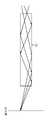
예를 들면, 도 3은 각형 광 파이버(13)를 통과하는 레이저광의 궤적의 예를 도시하고 있다. 도면 내의 화살표로 나타내어지는 바와 같이, 각형 광 파이버(13) 내의 상이한 궤적을 통과한 레이저광이, 조사면의 동일 위치에 조사되면, 각 레이저광의 파장이 동일하기 때문에 간섭이 일어난다. 그리고, 각형 광 파이버(13)로부터 출사된 동일한 파장의 레이저광이, 조사면에 있어서 불규칙한 위상 관계에 의해 서로 간섭하여, 불규칙한 간섭 패턴이 발생함으로써, 스페클이 증가하여, 광 강도 분포에 변동이 발생한다. 그 결과, 레이저 가공의 불균일이 발생하여, 가공 품질이 저하된다.For example, FIG. 3 shows an example of the locus of the laser light passing through the prismatic
따라서, 본 발명은, 레이저 발진기로부터 출사되는 레이저광을 광 파이버를 통과시킨 경우에, 단면의 광 강도 분포의 균일성을 향상시키도록 하는 것이다.Therefore, the present invention is intended to improve the uniformity of the light intensity distribution on the cross section when the laser beam emitted from the laser oscillator passes through the optical fiber.
본 발명의 제1 측면의 레이저 발진기는, 전반사면과 부분 반사면에 의해 구성되는 제1 광 공진기를 갖는 싱글 모드의 반도체 레이저와, 반도체 레이저의 부분 반사면으로부터 출사되는 광이 입사함과 함께, 반도체 레이저의 전반사면과의 사이에서 제2 광 공진기를 구성하는 회절 격자가 형성되어 있는 파이버 브래그 그레이팅과, 파이버 브래그 그레이팅으로부터 출사된 레이저광을 증폭하는 파이버 증폭기를 구비한다.A laser oscillator according to a first aspect of the present invention is a laser oscillator having a single mode semiconductor laser having a first optical resonator constituted by a total reflection plane and a partial reflection plane, A fiber Bragg grating in which a diffraction grating constituting a second optical resonator is formed between the optical waveguide and the total reflection plane of the semiconductor laser and a fiber amplifier for amplifying the laser light emitted from the fiber Bragg grating.
본 발명의 제1 측면의 레이저 발진기에 있어서는, 제1 광 공진기 및 제2 광 공진기에 의해, 상이한 파장의 레이저광이 발진된 후, 레이저광이 증폭된다.In the laser oscillator of the first aspect of the present invention, the laser light of different wavelength is oscillated by the first optical resonator and the second optical resonator, and then the laser light is amplified.
이에 의해, 레이저 발진기로부터 출사되는 레이저광의 스펙트럼 폭을 확장할 수 있다. 또한, 레이저 발진기로부터 출사되는 레이저광을 광 파이버를 통과시킨 경우에, 단면의 광 강도 분포의 균일성을 향상시킬 수 있다.As a result, the spectrum width of the laser beam emitted from the laser oscillator can be extended. In addition, when the laser beam emitted from the laser oscillator is passed through the optical fiber, the uniformity of the light intensity distribution on the end face can be improved.
이 파이버 브래그 그레이팅에는, 반사 대역이 상이한 복수의 회절 격자를 형성할 수 있다.In this fiber Bragg grating, a plurality of diffraction gratings having different reflection bands can be formed.
이에 의해, 간단한 구성에 의해, 레이저 발진기로부터 출사되는 레이저광의 스펙트럼 폭을 보다 확장할 수 있다.Thus, the spectral width of the laser beam emitted from the laser oscillator can be further expanded by a simple configuration.
이들 복수의 회절 격자의 각 반사 대역을, 인접하는 반사 대역의 일부와 겹치고, 복수의 회절 격자의 반사 대역을 중첩시킨 반사 대역을, 반도체 레이저의 피크 파장을 포함하도록 할 수 있다.The reflection band in which the respective reflection bands of the plurality of diffraction gratings are overlapped with a part of the adjacent reflection bands and the reflection bands of the plurality of diffraction gratings are overlapped can be made to include the peak wavelength of the semiconductor laser.
이 회절 격자의 반사 대역은, 반도체 레이저의 스펙트럼 폭보다 넓고, 반도체 레이저의 피크 파장을 포함하도록 할 수 있다.The reflection band of the diffraction grating is larger than the spectrum width of the semiconductor laser and can include the peak wavelength of the semiconductor laser.
이 파이버 증폭기로부터 출사된 레이저광을, 광 파이버를 통과시킨 후, 가공 대상물에 조사시키도록 할 수 있다.The laser beam emitted from the fiber amplifier can be irradiated to the object after passing through the optical fiber.
이에 의해, 단면의 광 강도 분포의 균일성이 높은 레이저광을 가공 대상물에 조사할 수 있어, 가공 품질이 향상된다.This makes it possible to irradiate an object to be processed with laser light having a high uniformity in the light intensity distribution on the cross section, thereby improving the processing quality.
본 발명의 제2 측면의 레이저 발진기는, 전반사면과 부분 반사면에 의해 구성되는 제1 광 공진기를 갖는 싱글 모드의 반도체 레이저와, 반도체 레이저의 부분 반사면으로부터 출사되는 광이 입사함과 함께, 반도체 레이저의 전반사면과의 사이에서 제2 광 공진기를 구성하는 회절 격자가 형성되어 있는 파이버 브래그 그레이팅을 구비하고, 파이버 브래그 그레이팅으로부터 출사되는 레이저광을 출사한다.A laser oscillator according to a second aspect of the present invention is a laser oscillator having a single mode semiconductor laser having a first optical resonator constituted by a total reflection surface and a partial reflection surface, And a fiber Bragg grating in which a diffraction grating constituting a second optical resonator is formed between the optical waveguide and the total reflection surface of the semiconductor laser, and the laser beam emitted from the fiber Bragg grating is emitted.
본 발명의 제2 측면의 레이저 발진기에 있어서는, 제1 광 공진기 및 제2 광 공진기에 의해, 상이한 파장의 레이저광이 발진된 후, 출사된다.In the laser oscillator of the second aspect of the present invention, laser light of a different wavelength is emitted by the first optical resonator and the second optical resonator, and then emitted.
이에 의해, 레이저 발진기로부터 출사되는 레이저광의 스펙트럼 폭을 확장할 수 있다. 또한, 레이저 발진기로부터 출사되는 레이저광을, 광 파이버를 통과시킨 경우에, 단면의 광 강도 분포의 균일성을 향상시킬 수 있다.As a result, the spectrum width of the laser beam emitted from the laser oscillator can be extended. In addition, when the laser beam emitted from the laser oscillator is passed through the optical fiber, the uniformity of the light intensity distribution on the cross section can be improved.
본 발명의 제1 측면 또는 제2 측면에 의하면, 레이저 발진기로부터 출사되는 레이저광의 스펙트럼 폭을 확장할 수 있다. 또한, 본 발명의 제1 측면 또는 제2 측면에 의하면, 레이저 발진기로부터 출사되는 레이저광을 광 파이버를 통과시킨 경우에, 단면의 광 강도 분포의 균일성을 향상시킬 수 있다.According to the first aspect or the second aspect of the present invention, the spectrum width of the laser beam emitted from the laser oscillator can be extended. Further, according to the first aspect or the second aspect of the present invention, when the laser beam emitted from the laser oscillator is passed through the optical fiber, the uniformity of the light intensity distribution on the cross section can be improved.
도 1은 종래의 레이저 가공 장치의 일례를 도시하는 도면.
도 2는 종래의 레이저 가공 장치로부터 출사되는 레이저광의 빔 프로파일의 예를 도시하는 도면.
도 3은 종래의 레이저 가공 장치의 각형 광 파이버를 통과하는 레이저광의 궤적의 예를 도시하는 도면.
도 4는 본 발명을 적용한 레이저 가공 장치의 일 실시 형태를 도시하는 도면.
도 5는 시드 LD의 구성예를 도시하는 도면.
도 6은 FBG의 구성예를 도시하는 도면.
도 7은 FBG의 반사 특성의 예를 도시하는 그래프.
도 8은 본 발명을 적용한 레이저 발진기의 레이저 발진의 원리를 설명하기 위한 도면.
도 9는 본 발명을 적용한 레이저 발진기로부터 출사되는 레이저광의 스펙트럼의 예를 도시하는 도면.
도 10은 본 발명을 적용한 레이저 가공 장치로부터 출사되는 레이저광의 빔 프로파일의 예를 도시하는 도면.
도 11은 본 발명을 적용한 레이저 가공 장치의 각형 광 파이버를 통과하는 레이저광의 궤적의 예를 도시하는 도면.1 is a view showing an example of a conventional laser machining apparatus.
2 is a view showing an example of a beam profile of laser light emitted from a conventional laser machining apparatus;
3 is a view showing an example of a locus of laser light passing through a prismatic optical fiber of a conventional laser machining apparatus;
4 is a diagram showing an embodiment of a laser machining apparatus to which the present invention is applied.
5 is a diagram showing a configuration example of a seed LD.
6 is a diagram showing a configuration example of an FBG;
7 is a graph showing an example of the reflection characteristic of the FBG;
8 is a view for explaining the principle of laser oscillation of a laser oscillator to which the present invention is applied.
9 is a view showing an example of a spectrum of laser light emitted from a laser oscillator to which the present invention is applied;
10 is a view showing an example of a beam profile of laser light emitted from a laser machining apparatus to which the present invention is applied;
11 is a diagram showing an example of a locus of laser light passing through a prismatic optical fiber of a laser machining apparatus to which the present invention is applied.
이하, 본 발명을 실시하기 위한 구체적인 내용(이하, 실시 형태라 함)에 대하여 설명한다. 또한, 설명은 이하의 순서로 행한다.Hereinafter, specific details (hereinafter referred to as embodiments) for carrying out the present invention will be described. The description will be made in the following order.
1. 실시 형태1. Embodiment
2. 변형예2. Variations
<1. 실시 형태><1. Embodiment>
[레이저 가공 장치의 구성예][Exemplary Configuration of Laser Processing Apparatus]
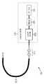
도 4는 본 발명을 적용한 레이저 가공 장치(101)의 일 실시 형태를 도시하고 있다. 레이저 가공 장치(101)는, 예를 들면 박막 태양 전지 패널이나 유기 EL 등의 가공에 사용된다. 또한, 레이저 가공 장치(101)는, 레이저 발진기(111), 렌즈계(112) 및 각형 광 파이버(113)를 포함하도록 구성된다.Fig. 4 shows an embodiment of a
레이저 발진기(111)는, 파이버 증폭기(123)에 의해 레이저광의 증폭을 행하는 파이버 레이저에 의해 구성되고, 시드 LD(레이저 다이오드)(121), 파이버 브래그 그레이팅(FBG)(122) 및 파이버 증폭기(123)를 포함하도록 구성된다.The laser oscillator 111 is constituted by a fiber laser that amplifies the laser light by the
시드 LD(121)는, 예를 들면 표준적인 싱글 모드의 반도체 레이저에 의해 구성되고, 소정 파장의 레이저광을 발진하고, 출사한다. 또한, 이하, 시드 LD(121)가, 피크 파장이 1062㎚인 레이저광을 발진하는 경우를 예로 들어 설명한다.The
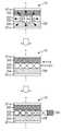
도 5는 시드 LD(121)의 구성예를 도시하고 있다. 시드 LD(121)는, +측의 전극(201a)과 -측의 전극(201b) 사이에, P형 반도체(202), 활성층(203) 및 N형 반도체(204)가 적층된 구성을 갖고 있다. 또한, 시드 LD(121)의 각 층에 대하여 수직인 방향의 측면이며, 서로 대향하는 측면의 한쪽에 전반사면(205)이 형성되고, 다른 쪽에 부분 반사면(206)이 형성되어 있다. 이 전반사면(205)과 부분 반사면(206)에 의해 광 공진기(이하, 내부 공진기라 칭함)가 구성된다.Fig. 5 shows a configuration example of the
도 4로 되돌아가서, FBG(122)는, 시드 LD(121)의 부분 반사면(206)측에 배치되며, 부분 반사면(206)으로부터 출사되는 광이 입사한다. FBG(122)는, 예를 들면 융착에 의해 시드 LD(121)에 접속된다.Returning to Fig. 4, the
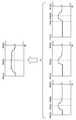
도 6은 FBG(122)의 구성예를 도시하고 있다. FBG(122)는, 코어(251)와 클래드(252)로 이루어지는 광 파이버의 코어(251) 중에, 중심 파장(브래그 파장)이 상이한 3개의 회절 격자(253a 내지 253c)를 광축 방향으로 배열하도록 형성한 것이다.6 shows an example of the configuration of the
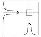
도 7은 회절 격자(253a 내지 253c) 및 FBG(122) 전체의 반사 특성의 예를 도시하고 있다. 구체적으로는, 도 7의 상측의 좌측 단부의 그래프는 회절 격자(253a)의 반사 특성을 나타내고, 한가운데의 그래프는 회절 격자(253b)의 반사 특성을 나타내고, 우측 단부의 그래프는 회절 격자(253c)의 반사 특성을 나타내고 있다. 또한, 도 7의 하측의 그래프는, FBG(122) 전체의 반사 특성을 나타내고 있다.7 shows examples of the reflection characteristics of the
회절 격자(253a 내지 253c)의 반사 대역의 대역 폭은, 표준적인 FBG의 회절 격자의 반사 대역보다 넓고, 또한, 시드 LD(121)의 스펙트럼 폭보다 넓게 되어 있다. 구체적으로는, 회절 격자(253a)의 반사 대역은, 1058㎚를 중심으로 하는 약 4㎚의 폭의 대역이다. 회절 격자(253b)의 반사 대역은, 시드 LD(121)의 피크 파장과 동일한 1062㎚를 중심으로 하는 약 4㎚의 폭의 대역이다. 회절 격자(253c)의 반사 대역은, 1066㎚를 중심으로 하는 약 4㎚의 폭의 대역이다.The band width of the reflection band of the
또한, 각 반사 대역은, 인접하는 반사 대역과 일부가 겹쳐 있다. 구체적으로는, 회절 격자(253a)의 반사 대역의 장파장측과, 회절 격자(253b)의 반사 대역의 단파장측이 일부 겹치고, 회절 격자(253b)의 반사 대역의 장파장측과, 회절 격자(253c)의 반사 대역의 단파장측이 일부 겹쳐 있다. 그리고, 회절 격자(253a 내지 253c)의 반사 대역을 중첩시킨 FBG(122) 전체의 반사 대역은, 1062㎚를 중심으로 하는 약 8㎚의 폭의 대역으로 된다.In addition, each reflection band partially overlaps with the adjacent reflection band. Specifically, the long wavelength side of the reflection band of the
이와 같이, 반사 대역이 상이한 복수의 회절 격자(253a 내지 253c)를 형성함으로써, 간단하게 반사 대역이 넓은 FBG(122)를 얻을 수 있다.By forming the plurality of
후술하는 바와 같이, 시드 LD(121)의 전반사면(205)과 FBG(122)의 회절 격자(253a 내지 253c)에 의해 3개의 광 공진기(이하, 외부 공진기라 칭함)가 구성되고, 각 외부 공진기에 있어서, 시드 LD(121)와는 상이한 파장의 레이저광이 발진한다. 그리고, 시드 LD(121) 단체에서 발진한 레이저광 및 각 외부 공진기에서 발진한 레이저광이, FBG(122)로부터 출사되어, 파이버 증폭기(123)에 입사한다.As described later, three optical resonators (hereinafter referred to as external resonators) are constituted by the
또한, 이하, 회절 격자(253a 내지 253c)를 개별적으로 구별할 필요가 없는 경우, 간단히, 회절 격자(253)라 칭한다.Hereinafter, when it is not necessary to distinguish the
도 4로 되돌아가서, 파이버 증폭기(123)는, 광 파이버를 매질로 하는 증폭기이며, FBG(122)로부터 출사된 레이저광을 증폭하여 출사한다. 파이버 증폭기(123)로부터 출사된 레이저광은, 렌즈계(112)에 의해 각형 광 파이버(113)에 도입된다.Returning to Fig. 4, the
각형 광 파이버(113)는, 코어의 단면이 직사각형이며, 입사한 레이저광의 단면을 직사각형으로 성형하여 출사한다. 또한, 후술하는 바와 같이, 각형 광 파이버(113)로부터 출사되는 레이저광은, 단면의 광 강도 분포의 균일성이 높은 플랫 톱 빔으로 된다.The prismatic
각형 광 파이버(113)로부터 출사된 레이저광은, 도시하지 않은 가공 광학계를 통하여, 예를 들면 박막 태양 전지 패널이나 유기 EL 등의 가공 대상물에 조사되어, 레이저 가공이 행해진다.The laser light emitted from the prismatic
[각형 광 파이버(113)로부터 출사되는 레이저광이 플랫 톱 빔으로 되는 원리][Principle that laser light emitted from prismatic
다음에, 도 8 내지 도 11을 참조하여, 각형 광 파이버(113)로부터 출사되는 레이저광이 플랫 빔으로 되는 원리에 대하여 설명한다.Next, with reference to Figs. 8 to 11, the principle that the laser beam emitted from the prismatic
도 8에 도시된 바와 같이, 시드 LD(21)의 전극(201a)과 전극(201b) 사이에 전압을 인가하면, 활성층(203)에 있어서 자연 방출광이 발생한다. 이 자연 방출광의 파장 특성은, 대략 가우스 분포에 따라서, 소정 파장(예를 들면, 1062㎚)을 중심으로 하는 비교적 넓은 대역 폭(예를 들면, 200㎚ 정도)을 갖고 있다. 그리고, 활성층(203)에 있어서, 이 자연 방출광을 시드광으로 하는 유도 방출이 발생되어, 유도 방출광이 발생한다. 또한, 전반사면(205)과 부분 반사면(206)으로 이루어지는 내부 공진기 사이를 자연 방출광 및 유도 방출광이 왕복하여, 유도 방출이 발생된다. 이때, 내부 공진기에 있어서, "내부 공진기의 공진기 길이=파장의 정수배"로 되는 파장의 광이 공진하여, 증폭된다. 이와 같이 하여, 소정 파장(예를 들면, 1062㎚)의 레이저광이 발진한다. 그리고, 발진한 레이저광, 및, 자연 방출광 및 유도 방출광의 일부를 포함하는 광이, 부분 반사면(206)으로부터 출사된다.8, spontaneous emission light is generated in the
또한, 부분 반사면(206)과 FBG(122)의 각 회절 격자(253)에 의해 구성되는 각 외부 공진기에 있어서도, 내부 공진기와 마찬가지로, 소정 파장의 레이저광이 발진한다. 그리고, 내부 공진기[시드 LD(121) 단체] 및 외부 공진기에 있어서 발진한 레이저광이, FBG(122)로부터 파이버 증폭기(123)를 향하여 출사된다.Also, in each of the external resonators constituted by the
여기서, 각 외부 공진기에 있어서, 각 회절 격자(253)의 반사 대역 내에서, 또한, "각 외부 공진기의 공진기 길이=파장의 정수배"로 되는 파장의 레이저광이 발진한다.Here, in each external resonator, a laser beam having a wavelength of "a resonator length of each external resonator = integer multiple of wavelength" oscillates within the reflection band of each
이와 같이, 시드 LD(21)(내부 공진기) 및 각 외부 공진기에 있어서, 시드 LD (21)의 피크 파장 및 당해 피크 파장 근방의 복수의 파장의 레이저광이 발진한다. 이에 의해, 시드 LD(121) 단체로부터 출사되는 레이저광보다 스펙트럼 폭이 넓은 레이저광이, 레이저 발진기(111)로부터 출사된다.As described above, the peak wavelength of the
도 9는 레이저 발진기(111)로부터 출사되는 레이저광의 스펙트럼의 일례이다. 이 예에 도시된 바와 같이, 레이저 발진기(111)로부터 출사되는 레이저광은, 시드 LD(121)의 피크 파장인 1062㎚ 외에, FBG(122)의 각 회절 격자(253)의 중심 파장 부근에도 피크가 나타남과 함께, 스펙트럼 폭이 확대되어 있다.9 is an example of the spectrum of the laser light emitted from the laser oscillator 111. Fig. As shown in this example, the laser light emitted from the laser oscillator 111 is incident on the
도 10은 각형 광 파이버(113)로부터 출사되는 레이저광의 조사면에 있어서의 빔 프로파일의 측정 결과를 모식적으로 도시하고 있다. 상술한 도 2의 예와 비교하면, 스페클이 감소하여, 광 강도 분포가 거의 균일해져 있다. 이것은, 종래의 레이저 발진기(11)(도 1)로부터 출사되는 레이저광과 비교하여, 레이저 발진기(111)로부터 출사되는 레이저광의 스펙트럼 폭이 넓고, 코히어런트성이 약함으로써, 레이저광의 간섭이 발생하기 어려워지기 때문이다.10 schematically shows the measurement result of the beam profile on the irradiation surface of the laser beam emitted from the prismatic
예를 들면, 도 11은, 도 1과 마찬가지로, 각형 광 파이버(113)로부터 출사되는 레이저광의 궤적의 예를 도시하고 있다. 또한, 각 화살표의 선의 종류의 차이는, 파장의 차이를 나타내고 있다. 이 도면과 같이, 상이한 파장의 레이저광이 조사면의 동일한 위치에 조사되었다고 해도, 각 레이저광은 간섭하지 않는다.For example, Fig. 11 shows an example of the locus of laser light emitted from the prismatic
그리고, 레이저광의 스펙트럼 폭이 넓어지고, 코히어런트성이 저하됨으로써, 각형 광 파이버(113) 내의 다른 궤적을 통과한 동일한 파장의 레이저광이, 조사면의 동일 위치에 조사되어, 간섭할 가능성이 낮아진다. 이에 의해, 조사면에 있어서 레이저광의 스페클이 감소하여, 광 강도 분포의 균일성이 향상된다. 그 결과, 레이저 가공의 불균일이 감소하여, 가공 품질이 향상된다.Since the spectral width of the laser beam is widened and the coherence property is lowered, the possibility that the laser beam of the same wavelength passing through another trajectory in the prismatic
또한, 레이저 발진기(111)는, 시드 LD(121)에 FBG(122)를 접속하는 것만의 간단한 구성에 의해 실현할 수 있기 때문에, 각종 조정 작업, 장치의 대형화, 비용의 상승 등의 발생을 억제할 수 있다.In addition, since the laser oscillator 111 can be realized by a simple configuration that connects the
또한, 레이저 가공 장치(101)는, 파이버 레이저로 이루어지는 레이저 발진기(111)를 사용하고 있기 때문에, 다른 고체 레이저를 사용한 경우와 비교하여, 레이저광의 반복 주파수, 펄스 폭, 출력 강도 등을 용이하게 독립하여 조정하는 것이 가능하다.Further, since the
<2. 변형예><2. Modifications>
이하, 상술한 본 발명의 실시 형태의 변형예에 대하여 설명한다.Modifications of the above-described embodiment of the present invention will be described below.
예를 들면, FBG(122)에 형성하는 회절 격자(253)의 수는, 3개로 한정되는 것은 아니고, 1 이상의 임의의 수로 설정할 수 있다.For example, the number of
또한, 회절 격자(253)의 반사 특성은, 도 7에 도시된 예에 한정되는 것은 아니고, 예를 들면 시드 LD(121)의 파장 특성 등에 따라서, 반사 대역의 중심 파장이나 대역 폭 등을 변경하는 것이 가능하다.The reflection characteristic of the
또한, 본 발명은, 코어의 단면이 직사각형 이외의 형상(예를 들면, 원형)의 광 파이버를 사용하는 경우에도 적용할 수 있다.The present invention can also be applied to the case where an optical fiber having a shape other than a rectangular cross section (for example, a circular shape) is used.
또한, 예를 들면 시드 LD(121)와 FBG(122)를 융착 등에 의해 물리적으로 접속하지 않고, 렌즈 등을 통하여, 광학적으로 접속하도록 해도 된다.Further, for example, the
또한, 예를 들면 시드 LD(121) 및 FBG(122)에 의해, 가공에 필요한 강도의 레이저광이 얻어지는 경우에는, 파이버 증폭기(123)를 설치하지 않도록 하는 것도 가능하다.In addition, for example, when the
또한, 본 발명은, FBG(122) 대신에, 시드 LD(121)의 전반사면과의 사이에서 외부 공진기를 구성하는 것이 가능한 광학 부품을 사용하는 것도 가능하다.In the present invention, it is also possible to use an optical component which can constitute an external resonator between the
또한, 본 기술의 실시 형태는, 상술한 실시 형태에 한정되는 것은 아니고, 본 기술의 요지를 일탈하지 않는 범위에서 다양한 변경이 가능하다.The embodiments of the present technology are not limited to the above-described embodiments, and various modifications can be made without departing from the gist of the present invention.
101 : 레이저 가공 장치
111 : 파이버 레이저
112 : 렌즈계
113 : 각형 광 파이버
121 : 시드 LD
122 : FBG
123 : 파이버 증폭기
201a, 201b : 전극
202 : P형 반도체
203 : 활성층
204 : N형 반도체
205 : 전반사면
206 : 부분 반사면
251 : 코어
252 : 클래드
253a 내지 253c : 회절 격자101: Laser processing device
111: Fiber laser
112: lens system
113: prismatic optical fiber
121: Seed LD
122: FBG
123: Fiber amplifier
201a, 201b: electrode
202: P-type semiconductor
203:
204: N-type semiconductor
205:
206: partial reflection surface
251: Core
252: clad
253a to 253c: a diffraction grating
Claims (6)
Translated fromKorean상기 반도체 레이저의 상기 부분 반사면으로부터 출사되는 광이 입사함과 함께, 상기 반도체 레이저의 상기 전반사면과의 사이에서 제2 광 공진기를 구성하는 회절 격자가 형성되어 있는 파이버 브래그 그레이팅과,
상기 파이버 브래그 그레이팅으로부터 출사된 레이저광을 증폭하는 파이버 증폭기를 구비하는, 레이저 발진기.A single mode semiconductor laser having a first optical resonator constituted by a total reflection plane and a partial reflection plane,
A fiber Bragg grating in which light emitted from the partial reflection surface of the semiconductor laser is incident and a diffraction grating constituting a second optical resonator is formed between the semiconductor laser and the total reflection surface of the semiconductor laser,
And a fiber amplifier for amplifying laser light emitted from the fiber Bragg grating.
상기 파이버 브래그 그레이팅에는, 반사 대역이 상이한 복수의 회절 격자가 형성되어 있는, 레이저 발진기.The method according to claim 1,
And a plurality of diffraction gratings having different reflection bands are formed in the fiber Bragg grating.
복수의 상기 회절 격자의 각 반사 대역은, 인접하는 반사 대역과 일부가 겹쳐 있고, 복수의 상기 회절 격자의 반사 대역을 중첩시킨 반사 대역은, 상기 반도체 레이저의 피크 파장을 포함하는, 레이저 발진기.3. The method of claim 2,
Each of the reflection bands of the plurality of diffraction gratings partially overlaps with the adjacent reflection bands and the reflection band in which the reflection bands of the plurality of diffraction gratings are overlapped includes the peak wavelength of the semiconductor laser.
상기 회절 격자의 반사 대역은, 상기 반도체 레이저의 스펙트럼 폭보다 넓고, 상기 반도체 레이저의 피크 파장을 포함하는, 레이저 발진기.The method according to claim 1,
Wherein a reflection band of the diffraction grating is wider than a spectral width of the semiconductor laser and includes a peak wavelength of the semiconductor laser.
상기 파이버 증폭기로부터 출사된 레이저광은, 광 파이버를 통과시킨 후, 가공 대상물에 조사되는, 레이저 발진기.The method according to claim 1,
Wherein the laser beam emitted from the fiber amplifier is irradiated to the object after passing through the optical fiber.
상기 반도체 레이저의 상기 부분 반사면으로부터 출사되는 광이 입사함과 함께, 상기 반도체 레이저의 상기 전반사면과의 사이에서 제2 광 공진기를 구성하는 회절 격자가 형성되어 있는 파이버 브래그 그레이팅을 구비하고,
상기 파이버 브래그 그레이팅으로부터 출사되는 레이저광을 출사하는, 레이저 발진기.A single mode semiconductor laser having a first optical resonator constituted by a total reflection plane and a partial reflection plane,
And a fiber Bragg grating in which light emitted from the partial reflection surface of the semiconductor laser is incident and a diffraction grating constituting a second optical resonator is formed between the semiconductor laser and the total reflection surface of the semiconductor laser,
And a laser beam emitted from the fiber Bragg grating is emitted.
Applications Claiming Priority (2)
| Application Number | Priority Date | Filing Date | Title |
|---|---|---|---|
| JP2013004707AJP6268706B2 (en) | 2013-01-15 | Laser oscillator | |
| JPJP-P-2013-004707 | 2013-01-15 |
Publications (1)
| Publication Number | Publication Date |
|---|---|
| KR20140092214Atrue KR20140092214A (en) | 2014-07-23 |
Family
ID=51146954
Family Applications (1)
| Application Number | Title | Priority Date | Filing Date |
|---|---|---|---|
| KR1020130152163ACeasedKR20140092214A (en) | 2013-01-15 | 2013-12-09 | Laser oscillator |
Country Status (3)
| Country | Link |
|---|---|
| US (1) | US20140198377A1 (en) |
| KR (1) | KR20140092214A (en) |
| CN (1) | CN103928827B (en) |
Families Citing this family (1)
| Publication number | Priority date | Publication date | Assignee | Title |
|---|---|---|---|---|
| JP2015005439A (en)* | 2013-06-21 | 2015-01-08 | スタンレー電気株式会社 | Vehicle headlamp and optical fiber bundle used for vehicle headlamp |
Family Cites Families (60)
| Publication number | Priority date | Publication date | Assignee | Title |
|---|---|---|---|---|
| US5043991A (en)* | 1989-12-28 | 1991-08-27 | General Dynamics Corp. Electronics Division | Device for compensating for thermal instabilities of laser diodes |
| US5134620A (en)* | 1990-11-20 | 1992-07-28 | General Instrument Corporation | Laser with longitudinal mode selection |
| US5151908A (en)* | 1990-11-20 | 1992-09-29 | General Instrument Corporation | Laser with longitudinal mode selection |
| US5191586A (en)* | 1991-07-18 | 1993-03-02 | General Instrument Corporation | Narrow band incoherent optical carrier generator |
| US5511083A (en)* | 1995-03-02 | 1996-04-23 | United Technologies Corporation | Polarized fiber laser source |
| US5594747A (en)* | 1995-03-06 | 1997-01-14 | Ball; Gary A. | Dual-wavelength pumped low noise fiber laser |
| US5696782A (en)* | 1995-05-19 | 1997-12-09 | Imra America, Inc. | High power fiber chirped pulse amplification systems based on cladding pumped rare-earth doped fibers |
| FR2736732B1 (en)* | 1995-07-13 | 1997-10-03 | Photonetics | STABILIZED WIDE SPECTRUM LIGHT SOURCE |
| EP0784362B1 (en)* | 1996-01-12 | 2003-03-26 | Corning O.T.I. S.p.A. | Rare-earth doped lithium niobate DBR laser |
| JP3120828B2 (en)* | 1996-04-08 | 2000-12-25 | 住友電気工業株式会社 | Semiconductor laser module |
| US5790722A (en)* | 1996-04-16 | 1998-08-04 | Hughes Electronics | High power optical fiber amplifier/laser system |
| US5912910A (en)* | 1996-05-17 | 1999-06-15 | Sdl, Inc. | High power pumped mid-IR wavelength systems using nonlinear frequency mixing (NFM) devices |
| GB9703078D0 (en)* | 1997-02-14 | 1997-04-02 | Univ Southampton | Optical fibre and optical fibre device |
| JP3206536B2 (en)* | 1997-02-21 | 2001-09-10 | 住友電気工業株式会社 | Semiconductor laser module |
| JPH1140883A (en)* | 1997-07-22 | 1999-02-12 | Ando Electric Co Ltd | Tunable semiconductor laser light source |
| US6049415A (en)* | 1997-12-08 | 2000-04-11 | Sdl, Inc. | Polarization maintaining fiber lasers and amplifiers |
| JPH11214799A (en)* | 1998-01-26 | 1999-08-06 | Furukawa Electric Co Ltd:The | Semiconductor laser module |
| US6195200B1 (en)* | 1998-02-18 | 2001-02-27 | Lucent Technologies Inc. | High power multiwavelength light source |
| US5966480A (en)* | 1998-02-23 | 1999-10-12 | Lucent Technologies Inc. | Article comprising an improved cascaded optical fiber Raman device |
| US6167066A (en)* | 1998-04-09 | 2000-12-26 | Hughes Electronics Corporation | Linearly-polarized, single-frequency fiber lasers |
| US6125222A (en)* | 1998-04-21 | 2000-09-26 | Scientific-Atlanta, Inc. | Fiber grating feedback stabilization of broad area laser diode |
| CA2269872A1 (en)* | 1998-04-23 | 1999-10-23 | Nec Corporation | A method of manufacturing a semiconductor optical waveguide array and an array-structured semiconductor optical device |
| JP4179662B2 (en)* | 1998-04-27 | 2008-11-12 | 富士通株式会社 | Optical amplifier and active optical fiber |
| AU3772099A (en)* | 1998-05-01 | 1999-11-23 | University Of New Mexico | Highly doped lasers and amplifiers |
| JP3097662B2 (en)* | 1998-06-08 | 2000-10-10 | 日本電気株式会社 | Optical fiber amplifier |
| US6188712B1 (en)* | 1998-11-04 | 2001-02-13 | Optigain, Inc. | Asymmetrical distributed feedback fiber laser |
| US6344921B1 (en)* | 1999-02-22 | 2002-02-05 | Almantas Galvanauskas | Optical parametric amplifiers and generators in optical communication systems |
| US6611369B2 (en)* | 1999-09-06 | 2003-08-26 | Furukawa Electric Co., Ltd. | Optical signal amplifier |
| US6407855B1 (en)* | 1999-10-29 | 2002-06-18 | Sdl, Inc. | Multiple wavelength optical sources |
| JP2001308454A (en)* | 2000-04-24 | 2001-11-02 | Fuji Photo Film Co Ltd | Light wavelength converting module |
| CA2343091C (en)* | 2000-05-25 | 2009-09-08 | Kyocera Corporation | Broadband amplified spontaneous emission light source |
| US6947463B2 (en)* | 2000-10-23 | 2005-09-20 | The Furukawa Electric Co., Ltd. | Semiconductor laser device for use in a laser module |
| US6507430B2 (en)* | 2001-02-23 | 2003-01-14 | Photon X, Inc. | Long wavelength optical amplifier |
| DE60209048T8 (en)* | 2001-03-09 | 2007-04-05 | Nippon Telegraph And Telephone Corp. | White light source |
| US6751241B2 (en)* | 2001-09-27 | 2004-06-15 | Corning Incorporated | Multimode fiber laser gratings |
| JP3682417B2 (en)* | 2001-05-01 | 2005-08-10 | 古河電気工業株式会社 | Semiconductor laser device, semiconductor laser module, and Raman amplifier using the same |
| JP2002341195A (en)* | 2001-05-16 | 2002-11-27 | Nec Corp | Semiconductor laser module |
| EP1271813B1 (en)* | 2001-06-29 | 2009-12-23 | Sumitomo Electric Industries, Ltd. | Pumping light source unit, raman amplifier, and optical transmission system |
| AU2002316478A1 (en)* | 2001-07-02 | 2003-01-21 | Ogg Technology Licensing, Llc. | Multi-wavelength optical fiber |
| US6693946B2 (en)* | 2001-07-05 | 2004-02-17 | Lucent Technologies Inc. | Wavelength-tunable lasers |
| US6580740B2 (en)* | 2001-07-18 | 2003-06-17 | The Furukawa Electric Co., Ltd. | Semiconductor laser device having selective absorption qualities |
| WO2003014771A2 (en)* | 2001-08-03 | 2003-02-20 | Ocg Technology Licensing, Llc | Optical fiber amplifier |
| US20030068125A1 (en)* | 2001-09-28 | 2003-04-10 | The Furukawa Electric Co., Ltd. | Semiconductor laser device, semiconductor laser module and optical fiber amplifier using the semiconductor laser module |
| US7116851B2 (en)* | 2001-10-09 | 2006-10-03 | Infinera Corporation | Optical signal receiver, an associated photonic integrated circuit (RxPIC), and method improving performance |
| US7283694B2 (en)* | 2001-10-09 | 2007-10-16 | Infinera Corporation | Transmitter photonic integrated circuits (TxPIC) and optical transport networks employing TxPICs |
| JP2003152274A (en)* | 2001-11-13 | 2003-05-23 | Furukawa Electric Co Ltd:The | Semiconductor laser device, semiconductor laser module, and Raman amplifier using the same |
| US6721088B2 (en)* | 2002-03-15 | 2004-04-13 | Ofs Fitel | Single-source multiple-order raman amplifier for optical transmission systems |
| FR2845833A1 (en)* | 2002-10-15 | 2004-04-16 | Cit Alcatel | SEMICONDUCTOR OPTICAL AMPLIFIER WITH LATERAL AND DISTRIBUTED GAIN STABILIZATION |
| US20050018732A1 (en)* | 2002-12-19 | 2005-01-27 | Aaron Bond | Uncooled and high temperature long reach transmitters, and high power short reach transmitters |
| US7190861B2 (en)* | 2003-01-15 | 2007-03-13 | Knopp Kevin J | Monolithic semiconductor light source with spectral controllability |
| JP4439193B2 (en)* | 2003-03-20 | 2010-03-24 | 富士通株式会社 | Semiconductor optical amplifier and optical amplification method |
| KR100559469B1 (en)* | 2003-06-09 | 2006-03-10 | 한국전자통신연구원 | Gain-clamped optical amplifier |
| KR100584413B1 (en)* | 2003-10-13 | 2006-05-26 | 삼성전자주식회사 | Broadband Light Source Using Semiconductor Optical Amplifier |
| KR100539906B1 (en)* | 2003-11-18 | 2005-12-28 | 삼성전자주식회사 | Reflective semiconductor optical amplifier light source |
| KR20050070566A (en)* | 2003-12-30 | 2005-07-07 | 삼성전자주식회사 | Multi-wavelength light source and wavelength-division multiplexing system using the same |
| US7693194B2 (en)* | 2004-08-12 | 2010-04-06 | Mitsubishi Electric Corporation | Fundamental-wave light source and wavelength converter |
| KR100987793B1 (en)* | 2008-10-10 | 2010-10-13 | 한국전자통신연구원 | Reflective semiconductor optical amplifier and optical signal processing method using same |
| GB2465754B (en)* | 2008-11-26 | 2011-02-09 | Univ Dublin City | A semiconductor optical amplifier with a reduced noise figure |
| KR101747153B1 (en)* | 2009-05-11 | 2017-06-14 | 오에프에스 피텔 엘엘씨 | Filter fiber for use in raman lasing applications and techniques for manufacturing same |
| KR20140011521A (en)* | 2012-06-27 | 2014-01-29 | 한국전자통신연구원 | External cavity laser using thin film filter and optical transmitter comprising external cavity laser |
- 2013
- 2013-12-09USUS14/100,300patent/US20140198377A1/ennot_activeAbandoned
- 2013-12-09KRKR1020130152163Apatent/KR20140092214A/ennot_activeCeased
- 2013-12-26CNCN201310738186.6Apatent/CN103928827B/enactiveActive
Also Published As
| Publication number | Publication date |
|---|---|
| US20140198377A1 (en) | 2014-07-17 |
| CN103928827B (en) | 2018-09-18 |
| JP2014138028A (en) | 2014-07-28 |
| CN103928827A (en) | 2014-07-16 |
Similar Documents
| Publication | Publication Date | Title |
|---|---|---|
| CN107615601B (en) | Laser module and laser processing device | |
| JP6807897B2 (en) | Reduction of laser spectral bandwidth | |
| CN109792129B (en) | Monolithic Visible Wavelength Fiber Laser | |
| EP2939316B1 (en) | Laser emitting apparatus and master oscillator power amplifier system | |
| US20180333807A1 (en) | Laser processing device, three-dimensional shaping device, and laser processing method | |
| US20230223735A1 (en) | Topologic insulator surface emitting laser system | |
| US12088060B2 (en) | Multi-wavelength laser generator using ring filter | |
| CN104321941A (en) | Pump radiation arrangement and method for pumping a laser-active medium | |
| US20180129059A1 (en) | Lighting apparatus with corresponding diffractive optical element | |
| US20210083458A1 (en) | Semiconductor optical amplifier | |
| KR20160045067A (en) | Ultra high power single mode fiber laser system | |
| US9490607B2 (en) | External cavity laser with single mode-hop-free tuning | |
| US20190013645A1 (en) | Wavelength Stabilized Diode Laser | |
| US10864600B2 (en) | Laser machining device | |
| KR20140092214A (en) | Laser oscillator | |
| US20220140563A1 (en) | Optical device and laser apparatus | |
| US10693273B2 (en) | Reflector, fiber cavity, and fiber laser | |
| JP6268706B2 (en) | Laser oscillator | |
| CN104600549A (en) | Mode-controllable coherent feedback optical fiber random laser device | |
| US20230134631A1 (en) | Asymmetric chirped fiber bragg grating for diode laser of fiber amplifier | |
| US10389087B2 (en) | Method and apparatus for spectral narrowing and wavelength stabilization of broad-area lasers | |
| Sumpf et al. | Comparison of electro-optical, spectral, and spatial beam parameters of 785 nm DBR tapered lasers with different grating lengths | |
| RU135193U1 (en) | SINGLE FREQUENCY TUNABLE SEMICONDUCTOR LASER | |
| Koyama | High Power VCSEL Amplifier for 3D Sensing | |
| US20250237821A1 (en) | Optical phased array, laser assembly and method for operating same |
Legal Events
| Date | Code | Title | Description |
|---|---|---|---|
| A201 | Request for examination | ||
| PA0109 | Patent application | Patent event code:PA01091R01D Comment text:Patent Application Patent event date:20131209 | |
| PA0201 | Request for examination | ||
| PG1501 | Laying open of application | ||
| PE0902 | Notice of grounds for rejection | Comment text:Notification of reason for refusal Patent event date:20140826 Patent event code:PE09021S01D | |
| E601 | Decision to refuse application | ||
| PE0601 | Decision on rejection of patent | Patent event date:20141224 Comment text:Decision to Refuse Application Patent event code:PE06012S01D Patent event date:20140826 Comment text:Notification of reason for refusal Patent event code:PE06011S01I |