KR20140086807A - Semiconductor structures and methods of forming the same - Google Patents
Semiconductor structures and methods of forming the sameDownload PDFInfo
- Publication number
- KR20140086807A KR20140086807AKR1020130102989AKR20130102989AKR20140086807AKR 20140086807 AKR20140086807 AKR 20140086807AKR 1020130102989 AKR1020130102989 AKR 1020130102989AKR 20130102989 AKR20130102989 AKR 20130102989AKR 20140086807 AKR20140086807 AKR 20140086807A
- Authority
- KR
- South Korea
- Prior art keywords
- gate stack
- gate
- dielectric layer
- thickness
- region
- Prior art date
- Legal status (The legal status is an assumption and is not a legal conclusion. Google has not performed a legal analysis and makes no representation as to the accuracy of the status listed.)
- Granted
Links
- 238000000034methodMethods0.000titleclaimsabstractdescription33
- 239000004065semiconductorSubstances0.000titledescription10
- 239000000758substrateSubstances0.000claimsabstractdescription39
- 229910052751metalInorganic materials0.000claimsdescription8
- 239000002184metalSubstances0.000claimsdescription8
- 239000010410layerSubstances0.000description112
- 239000011295pitchSubstances0.000description19
- 238000005530etchingMethods0.000description7
- 238000002955isolationMethods0.000description7
- 229920002120photoresistant polymerPolymers0.000description7
- 230000015572biosynthetic processEffects0.000description6
- 238000005229chemical vapour depositionMethods0.000description6
- 238000000151depositionMethods0.000description6
- 238000004519manufacturing processMethods0.000description6
- 125000006850spacer groupChemical group0.000description6
- XUIMIQQOPSSXEZ-UHFFFAOYSA-NSiliconChemical compound[Si]XUIMIQQOPSSXEZ-UHFFFAOYSA-N0.000description5
- 230000008901benefitEffects0.000description5
- 239000000463materialSubstances0.000description5
- 230000003647oxidationEffects0.000description5
- 238000007254oxidation reactionMethods0.000description5
- 229910052710siliconInorganic materials0.000description5
- 239000010703siliconSubstances0.000description5
- 238000000231atomic layer depositionMethods0.000description4
- 150000004767nitridesChemical class0.000description4
- 238000005240physical vapour depositionMethods0.000description4
- BASFCYQUMIYNBI-UHFFFAOYSA-NplatinumChemical compound[Pt]BASFCYQUMIYNBI-UHFFFAOYSA-N0.000description4
- 229910021332silicideInorganic materials0.000description4
- FVBUAEGBCNSCDD-UHFFFAOYSA-Nsilicide(4-)Chemical compound[Si-4]FVBUAEGBCNSCDD-UHFFFAOYSA-N0.000description4
- 229910052715tantalumInorganic materials0.000description4
- 229910052581Si3N4Inorganic materials0.000description3
- VYPSYNLAJGMNEJ-UHFFFAOYSA-NSilicium dioxideChemical compoundO=[Si]=OVYPSYNLAJGMNEJ-UHFFFAOYSA-N0.000description3
- 238000005516engineering processMethods0.000description3
- 238000004518low pressure chemical vapour depositionMethods0.000description3
- 230000000873masking effectEffects0.000description3
- 238000000623plasma-assisted chemical vapour depositionMethods0.000description3
- 238000012545processingMethods0.000description3
- HQVNEWCFYHHQES-UHFFFAOYSA-Nsilicon nitrideChemical compoundN12[Si]34N5[Si]62N3[Si]51N64HQVNEWCFYHHQES-UHFFFAOYSA-N0.000description3
- 229910052814silicon oxideInorganic materials0.000description3
- 239000000126substanceSubstances0.000description3
- GUVRBAGPIYLISA-UHFFFAOYSA-Ntantalum atomChemical compound[Ta]GUVRBAGPIYLISA-UHFFFAOYSA-N0.000description3
- 229910052719titaniumInorganic materials0.000description3
- 239000010936titaniumSubstances0.000description3
- KRHYYFGTRYWZRS-UHFFFAOYSA-NFluoraneChemical compoundFKRHYYFGTRYWZRS-UHFFFAOYSA-N0.000description2
- ZOKXTWBITQBERF-UHFFFAOYSA-NMolybdenumChemical compound[Mo]ZOKXTWBITQBERF-UHFFFAOYSA-N0.000description2
- PXHVJJICTQNCMI-UHFFFAOYSA-NNickelChemical compound[Ni]PXHVJJICTQNCMI-UHFFFAOYSA-N0.000description2
- KDLHZDBZIXYQEI-UHFFFAOYSA-NPalladiumChemical compound[Pd]KDLHZDBZIXYQEI-UHFFFAOYSA-N0.000description2
- KJTLSVCANCCWHF-UHFFFAOYSA-NRutheniumChemical compound[Ru]KJTLSVCANCCWHF-UHFFFAOYSA-N0.000description2
- RTAQQCXQSZGOHL-UHFFFAOYSA-NTitaniumChemical compound[Ti]RTAQQCXQSZGOHL-UHFFFAOYSA-N0.000description2
- 229910052782aluminiumInorganic materials0.000description2
- 238000004380ashingMethods0.000description2
- 229910017052cobaltInorganic materials0.000description2
- 239000010941cobaltSubstances0.000description2
- GUTLYIVDDKVIGB-UHFFFAOYSA-Ncobalt atomChemical compound[Co]GUTLYIVDDKVIGB-UHFFFAOYSA-N0.000description2
- 230000008021depositionEffects0.000description2
- 239000003989dielectric materialSubstances0.000description2
- 239000002019doping agentSubstances0.000description2
- 229910052735hafniumInorganic materials0.000description2
- 239000012535impuritySubstances0.000description2
- 229910044991metal oxideInorganic materials0.000description2
- 150000004706metal oxidesChemical class0.000description2
- 229910052750molybdenumInorganic materials0.000description2
- 239000011733molybdenumSubstances0.000description2
- 229910052697platinumInorganic materials0.000description2
- 229910052707rutheniumInorganic materials0.000description2
- -1titanium silicideChemical compound0.000description2
- WFKWXMTUELFFGS-UHFFFAOYSA-NtungstenChemical compound[W]WFKWXMTUELFFGS-UHFFFAOYSA-N0.000description2
- 229910052721tungstenInorganic materials0.000description2
- 239000010937tungstenSubstances0.000description2
- ZOXJGFHDIHLPTG-UHFFFAOYSA-NBoronChemical compound[B]ZOXJGFHDIHLPTG-UHFFFAOYSA-N0.000description1
- 229910052692DysprosiumInorganic materials0.000description1
- 229910052688GadoliniumInorganic materials0.000description1
- GYHNNYVSQQEPJS-UHFFFAOYSA-NGalliumChemical compound[Ga]GYHNNYVSQQEPJS-UHFFFAOYSA-N0.000description1
- 229910003855HfAlOInorganic materials0.000description1
- CBENFWSGALASAD-UHFFFAOYSA-NOzoneChemical compound[O-][O+]=OCBENFWSGALASAD-UHFFFAOYSA-N0.000description1
- OAICVXFJPJFONN-UHFFFAOYSA-NPhosphorusChemical compound[P]OAICVXFJPJFONN-UHFFFAOYSA-N0.000description1
- 229910000577Silicon-germaniumInorganic materials0.000description1
- ATJFFYVFTNAWJD-UHFFFAOYSA-NTinChemical compound[Sn]ATJFFYVFTNAWJD-UHFFFAOYSA-N0.000description1
- NRTOMJZYCJJWKI-UHFFFAOYSA-NTitanium nitrideChemical compound[Ti]#NNRTOMJZYCJJWKI-UHFFFAOYSA-N0.000description1
- HMDDXIMCDZRSNE-UHFFFAOYSA-N[C].[Si]Chemical compound[C].[Si]HMDDXIMCDZRSNE-UHFFFAOYSA-N0.000description1
- LEVVHYCKPQWKOP-UHFFFAOYSA-N[Si].[Ge]Chemical compound[Si].[Ge]LEVVHYCKPQWKOP-UHFFFAOYSA-N0.000description1
- 229910045601alloyInorganic materials0.000description1
- 239000000956alloySubstances0.000description1
- 230000004075alterationEffects0.000description1
- XAGFODPZIPBFFR-UHFFFAOYSA-NaluminiumChemical compound[Al]XAGFODPZIPBFFR-UHFFFAOYSA-N0.000description1
- 238000013459approachMethods0.000description1
- 229910052785arsenicInorganic materials0.000description1
- RQNWIZPPADIBDY-UHFFFAOYSA-Narsenic atomChemical compound[As]RQNWIZPPADIBDY-UHFFFAOYSA-N0.000description1
- 229910052788bariumInorganic materials0.000description1
- 229910052796boronInorganic materials0.000description1
- 230000003247decreasing effectEffects0.000description1
- 238000013461designMethods0.000description1
- 238000011161developmentMethods0.000description1
- 238000007598dipping methodMethods0.000description1
- 230000006870functionEffects0.000description1
- 229910052733galliumInorganic materials0.000description1
- VBJZVLUMGGDVMO-UHFFFAOYSA-Nhafnium atomChemical compound[Hf]VBJZVLUMGGDVMO-UHFFFAOYSA-N0.000description1
- 229910000449hafnium oxideInorganic materials0.000description1
- WIHZLLGSGQNAGK-UHFFFAOYSA-Nhafnium(4+);oxygen(2-)Chemical compound[O-2].[O-2].[Hf+4]WIHZLLGSGQNAGK-UHFFFAOYSA-N0.000description1
- 229910052738indiumInorganic materials0.000description1
- APFVFJFRJDLVQX-UHFFFAOYSA-Nindium atomChemical compound[In]APFVFJFRJDLVQX-UHFFFAOYSA-N0.000description1
- 239000012212insulatorSubstances0.000description1
- 239000011229interlayerSubstances0.000description1
- 229910052746lanthanumInorganic materials0.000description1
- 229910052745leadInorganic materials0.000description1
- 150000002739metalsChemical class0.000description1
- 239000000203mixtureSubstances0.000description1
- 229910052759nickelInorganic materials0.000description1
- 229910052758niobiumInorganic materials0.000description1
- 239000010955niobiumSubstances0.000description1
- GUCVJGMIXFAOAE-UHFFFAOYSA-Nniobium atomChemical compound[Nb]GUCVJGMIXFAOAE-UHFFFAOYSA-N0.000description1
- 229910052763palladiumInorganic materials0.000description1
- 229910052698phosphorusInorganic materials0.000description1
- 239000011574phosphorusSubstances0.000description1
- 238000000206photolithographyMethods0.000description1
- 238000002294plasma sputter depositionMethods0.000description1
- 229910021420polycrystalline siliconInorganic materials0.000description1
- 229920005591polysiliconPolymers0.000description1
- 150000004760silicatesChemical class0.000description1
- HBMJWWWQQXIZIP-UHFFFAOYSA-Nsilicon carbideChemical compound[Si+]#[C-]HBMJWWWQQXIZIP-UHFFFAOYSA-N0.000description1
- 229910010271silicon carbideInorganic materials0.000description1
- 229910052712strontiumInorganic materials0.000description1
- 238000006467substitution reactionMethods0.000description1
- MZLGASXMSKOWSE-UHFFFAOYSA-Ntantalum nitrideChemical compound[Ta]#NMZLGASXMSKOWSE-UHFFFAOYSA-N0.000description1
- 229910021341titanium silicideInorganic materials0.000description1
- 238000012546transferMethods0.000description1
- XLYOFNOQVPJJNP-UHFFFAOYSA-NwaterChemical compoundOXLYOFNOQVPJJNP-UHFFFAOYSA-N0.000description1
- 229910052727yttriumInorganic materials0.000description1
- 229910052725zincInorganic materials0.000description1
- 229910052726zirconiumInorganic materials0.000description1
Images


Classifications
- H—ELECTRICITY
- H10—SEMICONDUCTOR DEVICES; ELECTRIC SOLID-STATE DEVICES NOT OTHERWISE PROVIDED FOR
- H10D—INORGANIC ELECTRIC SEMICONDUCTOR DEVICES
- H10D84/00—Integrated devices formed in or on semiconductor substrates that comprise only semiconducting layers, e.g. on Si wafers or on GaAs-on-Si wafers
- H10D84/01—Manufacture or treatment
- H10D84/0123—Integrating together multiple components covered by H10D12/00 or H10D30/00, e.g. integrating multiple IGBTs
- H10D84/0126—Integrating together multiple components covered by H10D12/00 or H10D30/00, e.g. integrating multiple IGBTs the components including insulated gates, e.g. IGFETs
- H10D84/0165—Integrating together multiple components covered by H10D12/00 or H10D30/00, e.g. integrating multiple IGBTs the components including insulated gates, e.g. IGFETs the components including complementary IGFETs, e.g. CMOS devices
- H10D84/0172—Manufacturing their gate conductors
- H10D84/0179—Manufacturing their gate conductors the gate conductors having different shapes or dimensions
- H—ELECTRICITY
- H10—SEMICONDUCTOR DEVICES; ELECTRIC SOLID-STATE DEVICES NOT OTHERWISE PROVIDED FOR
- H10D—INORGANIC ELECTRIC SEMICONDUCTOR DEVICES
- H10D30/00—Field-effect transistors [FET]
- H10D30/01—Manufacture or treatment
- H10D30/021—Manufacture or treatment of FETs having insulated gates [IGFET]
- H10D30/0415—Manufacture or treatment of FETs having insulated gates [IGFET] of FETs having ferroelectric gate insulators
- H—ELECTRICITY
- H10—SEMICONDUCTOR DEVICES; ELECTRIC SOLID-STATE DEVICES NOT OTHERWISE PROVIDED FOR
- H10D—INORGANIC ELECTRIC SEMICONDUCTOR DEVICES
- H10D84/00—Integrated devices formed in or on semiconductor substrates that comprise only semiconducting layers, e.g. on Si wafers or on GaAs-on-Si wafers
- H10D84/01—Manufacture or treatment
- H10D84/0123—Integrating together multiple components covered by H10D12/00 or H10D30/00, e.g. integrating multiple IGBTs
- H10D84/0126—Integrating together multiple components covered by H10D12/00 or H10D30/00, e.g. integrating multiple IGBTs the components including insulated gates, e.g. IGFETs
- H10D84/0135—Manufacturing their gate conductors
- H—ELECTRICITY
- H10—SEMICONDUCTOR DEVICES; ELECTRIC SOLID-STATE DEVICES NOT OTHERWISE PROVIDED FOR
- H10D—INORGANIC ELECTRIC SEMICONDUCTOR DEVICES
- H10D84/00—Integrated devices formed in or on semiconductor substrates that comprise only semiconducting layers, e.g. on Si wafers or on GaAs-on-Si wafers
- H10D84/01—Manufacture or treatment
- H10D84/0123—Integrating together multiple components covered by H10D12/00 or H10D30/00, e.g. integrating multiple IGBTs
- H10D84/0126—Integrating together multiple components covered by H10D12/00 or H10D30/00, e.g. integrating multiple IGBTs the components including insulated gates, e.g. IGFETs
- H10D84/0144—Manufacturing their gate insulating layers
- H—ELECTRICITY
- H10—SEMICONDUCTOR DEVICES; ELECTRIC SOLID-STATE DEVICES NOT OTHERWISE PROVIDED FOR
- H10D—INORGANIC ELECTRIC SEMICONDUCTOR DEVICES
- H10D84/00—Integrated devices formed in or on semiconductor substrates that comprise only semiconducting layers, e.g. on Si wafers or on GaAs-on-Si wafers
- H10D84/01—Manufacture or treatment
- H10D84/0123—Integrating together multiple components covered by H10D12/00 or H10D30/00, e.g. integrating multiple IGBTs
- H10D84/0126—Integrating together multiple components covered by H10D12/00 or H10D30/00, e.g. integrating multiple IGBTs the components including insulated gates, e.g. IGFETs
- H10D84/0165—Integrating together multiple components covered by H10D12/00 or H10D30/00, e.g. integrating multiple IGBTs the components including insulated gates, e.g. IGFETs the components including complementary IGFETs, e.g. CMOS devices
- H10D84/0181—Manufacturing their gate insulating layers
- H—ELECTRICITY
- H10—SEMICONDUCTOR DEVICES; ELECTRIC SOLID-STATE DEVICES NOT OTHERWISE PROVIDED FOR
- H10D—INORGANIC ELECTRIC SEMICONDUCTOR DEVICES
- H10D84/00—Integrated devices formed in or on semiconductor substrates that comprise only semiconducting layers, e.g. on Si wafers or on GaAs-on-Si wafers
- H10D84/01—Manufacture or treatment
- H10D84/02—Manufacture or treatment characterised by using material-based technologies
- H10D84/03—Manufacture or treatment characterised by using material-based technologies using Group IV technology, e.g. silicon technology or silicon-carbide [SiC] technology
- H10D84/038—Manufacture or treatment characterised by using material-based technologies using Group IV technology, e.g. silicon technology or silicon-carbide [SiC] technology using silicon technology, e.g. SiGe
- H—ELECTRICITY
- H10—SEMICONDUCTOR DEVICES; ELECTRIC SOLID-STATE DEVICES NOT OTHERWISE PROVIDED FOR
- H10D—INORGANIC ELECTRIC SEMICONDUCTOR DEVICES
- H10D84/00—Integrated devices formed in or on semiconductor substrates that comprise only semiconducting layers, e.g. on Si wafers or on GaAs-on-Si wafers
- H10D84/80—Integrated devices formed in or on semiconductor substrates that comprise only semiconducting layers, e.g. on Si wafers or on GaAs-on-Si wafers characterised by the integration of at least one component covered by groups H10D12/00 or H10D30/00, e.g. integration of IGFETs
- H10D84/82—Integrated devices formed in or on semiconductor substrates that comprise only semiconducting layers, e.g. on Si wafers or on GaAs-on-Si wafers characterised by the integration of at least one component covered by groups H10D12/00 or H10D30/00, e.g. integration of IGFETs of only field-effect components
- H10D84/83—Integrated devices formed in or on semiconductor substrates that comprise only semiconducting layers, e.g. on Si wafers or on GaAs-on-Si wafers characterised by the integration of at least one component covered by groups H10D12/00 or H10D30/00, e.g. integration of IGFETs of only field-effect components of only insulated-gate FETs [IGFET]
- H10D84/85—Complementary IGFETs, e.g. CMOS
Landscapes
- Metal-Oxide And Bipolar Metal-Oxide Semiconductor Integrated Circuits (AREA)
- Electrodes Of Semiconductors (AREA)
- Insulated Gate Type Field-Effect Transistor (AREA)
Abstract
Translated fromKorean
Description
Translated fromKorean본 출원은 발명의 명칭이 "Novel Power Gating Approach on TGO Devices in HKMG CMOS Technology"이고 2012년 12월 28일자에 출원된 미국 가특허 번호 제61/747,106호의 우선권을 주장하고, 이 출원은 참조에 의해 그 전체가 본 명세서에 통합된다.This application claims the benefit of US Patent No. 61 / 747,106, filed December 28, 2012, entitled " Novel Power Gating Approach on TGO Devices in HKMG CMOS Technology, " The entirety of which is incorporated herein by reference.
반도체 집적 회로(IC) 산업은 급속한 성장을 이루었다. IC 물질 및 설계에서 기술적 진보는 IC 세대를 만들었고, 각각의 세대는 이전 세대보다 더욱 작고 더욱 복잡한 회로를 갖는다. 그러나, 이러한 진보는 IC 제조 및 처리의 복잡성을 증가시키고, 이러한 진보를 실현하기 위해, IC 제조 및 처리에서 유사한 개발이 필요하다.The semiconductor integrated circuit (IC) industry has achieved rapid growth. Technological advances in IC materials and design have created IC generations, each with smaller and more complex circuits than previous generations. However, these advances increase the complexity of IC fabrication and processing and require similar development in IC fabrication and processing to realize this advance.
IC 진화 동안에, 피처 크기[예컨대, 제조 공정을 이용하여 생성될 수 있는 가장 작은 컴포넌트(또는 라인)]는 감소한 반면, 기능 밀도(예컨대, 칩 영역당 상호접속된 디바이스의 수)는 일반적으로 증가하였다. 이러한 축소 공정은 일반적으로 생산 효율성을 증가시키고 관련 비용을 낮춤으로써 이점을 제공한다. 그러나, 디바이스를 지속적으로 축소시킴으로써, 상호접속된 디바이스들의 다양한 성능 특성들 간의 차이가 악화될 수 있다.During IC evolution, the feature size (e.g., the smallest component (or line) that can be generated using a fabrication process) has decreased while the functional density (e.g., the number of interconnected devices per chip area) has generally increased . This shrinking process generally offers benefits by increasing production efficiency and lowering the associated costs. However, by continuously shrinking the device, the difference between the various performance characteristics of the interconnected devices may deteriorate.
본 발명의 목적은 반도체 구조물 및 반도체 구조물을 형성하는 방법을 제공하는 것이다.It is an object of the present invention to provide a method of forming a semiconductor structure and a semiconductor structure.
실시예는 구조물이다. 구조물은 기판의 각각 3개의 영역에 3개의 디바이스들을 포함한다. 제 1 디바이스는 제 1 게이트 스택을 포함하고, 제 1 게이트 스택은 제 1 유전층을 포함한다. 제 2 디바이스는 제 2 게이트 스택을 포함하고, 제 2 게이트 스택은 제 2 유전층을 포함한다. 제 3 디바이스는 제 3 게이트 스택을 포함하고, 제 3 게이트 스택은 제 3 유전층을 포함한다. 제 3 유전층의 두께는 제 2 유전층의 두께보다 얇고, 제 2 유전층의 두께는 제 1 유전층의 두께보다 얇다. 제 3 게이트 스택의 게이트 길이는 결국 제 1 게이트 스택의 게이트 길이 및 제 2 게이트 스택의 게이트 길이와 상이하다.An embodiment is a structure. The structure includes three devices in each of three regions of the substrate. The first device comprises a first gate stack, wherein the first gate stack comprises a first dielectric layer. The second device comprises a second gate stack, and the second gate stack comprises a second dielectric layer. The third device comprises a third gate stack, and the third gate stack comprises a third dielectric layer. The thickness of the third dielectric layer is thinner than the thickness of the second dielectric layer, and the thickness of the second dielectric layer is thinner than the thickness of the first dielectric layer. The gate length of the third gate stack eventually differs from the gate length of the first gate stack and the gate length of the second gate stack.
다른 실시예는 구조물이다. 구조물은 기판의 제 1 영역, 제 2 영역 및 제 3 영역을 포함한다. 제 1 영역은 제 1 디바이스 및 제 2 디바이스를 포함한다. 제 2 영역은 제 3 디바이스 및 제 4 디바이스를 포함한다. 제 3 영역은 제 5 디바이스 및 제 6 디바이스를 포함한다. 제 1 디바이스, 제 2 디바이스, 제 3 디바이스, 제 4 디바이스, 제 5 디바이스 및 제 6 디바이스는 제 1 게이트 스택, 제 2 게이트 스택, 제 3 게이트 스택, 제 4 게이트 스택, 제 5 게이트 스택, 및 제 6 게이트 스택을 각각 포함한다. 제 1 게이트 스택 및 제 2 게이트 스택 각각은 제 1 두께를 갖는 제 1 유전층을 포함한다. 제 3 게이트 스택 및 제 4 게이트 스택 각각은 제 2 두께를 갖는 제 2 유전층을 포함한다. 제 5 게이트 스택 및 제 6 게이트 스택 각각은 제 3 두께를 갖는 제 3 유전층을 포함한다. 제 3 두께는 제 2 두께보다 크고, 제 2 두께는 제 1 두께보다 크다. 제 1 게이트 스택, 제 2 게이트 스택, 제 3 게이트 스택, 제 4 게이트 스택, 제 5 게이트 스택, 및 제 6 게이트 스택은 각각 제 1 게이트 스택, 제 2 게이트 스택, 제 3 게이트 스택, 제 4 게이트 스택, 제 5 게이트 스택, 및 제 6 게이트 스택의 대향하는 측벽들 사이에 각각의 길이를 갖는다. 제 1 길이 및 제 2 길이 각각은 제 3 길이, 제 4 길이, 제 5 길이 및 제 6 길이 각각의 치수와 상이하다. 제 1 피치는 제 1 게이트 스택과 제 2 게이트 스택 사이이다. 제 2 피치는 제 3 게이트 스택과 제 4 게이트 스택 사이이다. 제 3 피치는 제 5 게이트 스택과 제 6 게이트 스택 사이이다.Another embodiment is a structure. The structure includes a first region, a second region and a third region of the substrate. The first area includes a first device and a second device. And the second area includes a third device and a fourth device. And the third area includes a fifth device and a sixth device. The first device, the second device, the third device, the fourth device, the fifth device, and the sixth device may include a first gate stack, a second gate stack, a third gate stack, a fourth gate stack, And a sixth gate stack, respectively. Each of the first gate stack and the second gate stack includes a first dielectric layer having a first thickness. Each of the third gate stack and the fourth gate stack includes a second dielectric layer having a second thickness. Each of the fifth gate stack and the sixth gate stack includes a third dielectric layer having a third thickness. The third thickness is greater than the second thickness, and the second thickness is greater than the first thickness. The first gate stack, the second gate stack, the third gate stack, the fourth gate stack, the fifth gate stack, and the sixth gate stack each have a first gate stack, a second gate stack, a third gate stack, Stack, the fifth gate stack, and the opposing sidewalls of the sixth gate stack. Each of the first length and the second length is different from the dimensions of the third length, the fourth length, the fifth length and the sixth length, respectively. The first pitch is between the first gate stack and the second gate stack. The second pitch is between the third gate stack and the fourth gate stack. The third pitch is between the fifth gate stack and the sixth gate stack.
추가의 실시예는 방법이다. 방법은 기판의 제 1 영역에 제 1 유전층을 형성하는 단계, 기판의 제 2 영역에 제 2 유전층을 형성하는 단계, 기판의 제 3 영역에 제 3 유전층을 형성하는 단계, 제 1 유전층을 포함하는 제 1 게이트 스택을 형성하는 단계, 제 2 유전층을 포함하는 제 2 게이트 스택을 형성하는 단계, 및 제 3 유전층을 포함하는 제 3 게이트 스택을 형성하는 단계를 포함한다. 제 1 유전층은 제 1 두께를 갖고, 제 2 유전층은 제 2 두께를 갖고, 제 3 유전층은 제 3 두께를 갖는다. 제 1 두께는 제 2 두께보다 크고, 제 2 두께는 제 3 두께보다 크다. 제 1 게이트 스택은 제 1 게이트 길이를 갖고, 제 2 게이트 스택은 제 2 게이트 길이를 갖고, 제 3 게이트 스택은 제 3 게이트 길이를 갖는다. 제 3 게이트 길이는 제 1 게이트 길이 및 제 2 게이트 길이보다 크거나 작다.A further embodiment is the method. The method includes the steps of forming a first dielectric layer in a first region of a substrate, forming a second dielectric layer in a second region of the substrate, forming a third dielectric layer in a third region of the substrate, Forming a first gate stack, forming a second gate stack comprising a second dielectric layer, and forming a third gate stack comprising a third dielectric layer. The first dielectric layer has a first thickness, the second dielectric layer has a second thickness, and the third dielectric layer has a third thickness. The first thickness is greater than the second thickness, and the second thickness is greater than the third thickness. The first gate stack has a first gate length, the second gate stack has a second gate length, and the third gate stack has a third gate length. The third gate length is greater than or less than the first gate length and the second gate length.
본 발명에 따르면, 반도체 구조물 및 반도체 구조물을 형성하는 방법을 제공하는 것이 가능하다.According to the present invention, it is possible to provide a method of forming a semiconductor structure and a semiconductor structure.
본 실시예 및 본 실시예의 장점의 보다 완벽한 이해를 위해, 이제부터 첨부된 도면들을 참조하면서 이하의 상세한 설명에 대해 설명을 한다.
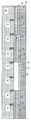
도 1 내지 도 8은 실시예에 따른 공정 흐름 및 구조물을 나타낸다.BRIEF DESCRIPTION OF THE DRAWINGS For a more complete understanding of the present embodiments and advantages thereof, reference is now made to the following detailed description taken in conjunction with the accompanying drawings, in which: FIG.
Figures 1-8 illustrate process flows and structures according to embodiments.
이하에서는 본 실시예들의 제조 및 이용을 자세하게 설명한다. 하지만, 본 발명개시는 폭넓은 다양한 특정한 상황에서 구현될 수 있는 수많은 적용 가능한 발명의 개념을 제공한다는 점을 이해해야 한다. 설명하는 특정한 실시예들은 개시된 주제를 제조하고 이용하는 특정한 방법들에 대한 단순한 예시에 불과하며, 상이한 실시예들의 범위를 한정시키려는 것은 아니다.Hereinafter, the manufacture and use of the embodiments will be described in detail. However, it should be understood that the disclosure of the present invention provides a number of applicable inventive concepts that can be implemented in a wide variety of specific contexts. The particular embodiments described are merely illustrative of specific ways of making and using the disclosed subject matter and are not intended to limit the scope of the different embodiments.
실시예들은 특정한 상황 즉, 반도체 디바이스를 형성하기 위한 공정에 관하여 기술될 것이고, 여기서 디바이스들 중 적어도 3개의 디바이스들은 디바이스들 간의 상이한 두께를 갖는 게이트 스택의 유전층을 포함한다. 더욱이, 디바이스들의 게이트 길이가 다양한 방식으로 바이어스될 수 있다. 다른 실시예들은 디바이스들의 수 및/또는 유전층의 두께를 변화시키는 것은 물론, 바이어싱을 다르게 하는 것을 고려한다. 이하에 특별한 순서로 기술되었지만, 방법 실시예들은 임의의 논리적인 순서로 수행될 수 있다. 부가적으로, 도면에서 사용되는 동일한 참조 번호는 동일한 컴포넌트를 나타낸다.Embodiments will be described with respect to a particular situation, i.e., a process for forming a semiconductor device, wherein at least three of the devices include a dielectric layer of a gate stack having different thicknesses between the devices. Moreover, the gate lengths of the devices can be biased in a variety of ways. Other embodiments contemplate different biasing as well as varying the number of devices and / or the thickness of the dielectric layer. Although described in a particular order below, method embodiments may be performed in any logical order. Additionally, like reference numerals used in the drawings denote like components.
도 1 내지 도 8은 실시예에 따른 공정 흐름 및 구조물을 나타낸다. 도 1은 기판(20)을 나타낸다. 기판(20)은 반도체 기판일 수 있고, 반도체 기판은 또한 실리콘 기판, 실리콘 탄소 기판, 실리콘 게르마늄 기판, 또는 다른 반도체 물질로 형성된 기판일 수 있다. 기판(20)은 벌크 기판, 실리콘 온 인슐레이터(semiconductor-on-insulator; SOI) 기판, 또는 다른 수용 가능한 기판일 수 있다. 기판(20)은 p형 불순물 또는 n형 불순물로 경도핑(lightly dope)될 수 있다. 기판(20)의 제 1 영역(22), 제 2 영역(24), 제 3 영역(26), 및 제 4 영역(28)이 도 1에서 식별된다. 실시예에서, 제 1 영역(22)은 코어 회로를 위한 디바이스들을 포함하는 것과 같은 얇은 코어 영역으로, 여기서 트랜지스터들은 얇은 게이트 유전체를 갖고; 제 2 영역(24)은 코어 회로를 위한 디바이스들을 포함하는 것과 같은 두꺼운 코어 영역으로, 여기서 트랜지스터들은 비교적 두꺼운 게이트 유전체를 갖고; 제 3 영역(26)은 신호를 입력 및/또는 출력하는데 이용되는 디바이스들을 포함하는 것과 같은 입출력 영역이며; 제 4 영역(28)은 SRAM 영역과 같은 메모리 영역이다.Figures 1-8 illustrate process flows and structures according to embodiments. Figure 1 shows a
기판(20)은 쉘로우 트렌치 분리 영역과 같은 분리 영역(30)을 더 포함한다. 분리 영역(30)은 기판(20)에서 별도의 디바이스들의 활성 영역들을 전기적으로 분리시키는데 이용될 수 있다. 일부 분리 영역(30)은 제 1 영역(22), 제 2 영역(24), 제 3 영역(26) 및 제 4 영역(28) 중 인접한 영역들 간의 경계들을 각각 디마크(demark)할 수 있다. 분리 영역(30)의 형성은 트렌치(도시되지 않음)를 형성하기 위해 기판(20)을 에칭하는 단계, 및 분리 영역(30)을 형성하기 위해 유전체 물질로 트렌치를 충진하는 단계를 포함할 수 있다. 분리 영역(30)은 예를 들어 고밀도 플라즈마에 의해 퇴적된 실리콘 산화물로 형성될 수 있지만, 다양한 기술에 따라 형성된 다른 유전체 물질들이 또한 이용될 수 있다.The
제 1 유전층(32)이 기판(20) 위에 형성된다. 실시예에서, 제 1 유전층(32)은 열 산화, 고밀도 플라즈마 퇴적 등에 의해 형성된 산화층이다. 다른 실시예들에서, 제 1 유전층(32)은 임의의 수용 가능한 기술에 의해 형성된 실리콘 산화질화물 등일 수 있다. 제 1 유전층(32)은 대략 25 Å와 대략 40 Å 사이의 두께를 가질 수 있다. 특정한 두께가 본 명세서에 예로서 제공되었지만, 상이한 실시예들은 예컨대 상이한 기술 크기의 경우 다른 두께를 가질 수 있다.A first
도 2는 제 2 영역(24) 및 제 4 영역(28)에 두꺼운 계면층(36)의 형성을 나타낸다. 제 1 유전층(32)은 예를 들어 제 2 영역(24) 및 제 4 영역(28)을 노출하면서 제 1 영역(22) 및 제 3 영역(26)을 커버하기 위해 제 1 유전층(32) 위에 포토레지스트(34)를 패턴화하고, 그 후에 예컨대 저농도 불화 수소산(dilute hydrofluoric acid; dHF)에 담그는 것에 의해 제 1 유전층(32)의 노출된 부분을 에칭함으로써 제 2 영역(24) 및 제 4 영역(28)으로부터 제거된다. 두꺼운 계면층(36)이 제 2 영역(24) 및 제 4 영역(28)에 있는 기판(20) 상에 퇴적된다. 두꺼운 계면층(36)은 실리콘 산화물, 실리콘 질화물, 실리콘 산화질화물 등 또는 이들의 조합을 포함할 수 있고, 열 산화 또는 화학적 산화[예를 들어, 오존 탈이온(de-ionized; DI)수에 담금], 적절한 퇴적 기술 등을 이용하여 형성될 수 있다. 실시예에서, 두꺼운 계면층(36)은 대략 10 Å와 대략 20 Å 사이의 두께를 갖는다. 실시예에서, 두꺼운 계면층(36)은 제 1 유전층(32)의 두께보다 얇은 두께를 갖는다. 그 후에, 포토레지스트(34)는 예를 들어 적절한 애싱 공정을 이용하여 제거될 수 있다.Figure 2 shows the formation of a
도 3은 제 1 영역(22)에 얇은 계면층(40)의 형성을 나타낸다. 제 1 유전층(32)은 예를 들어 제 1 영역(22)을 노출하면서 제 3 영역(26)의 제 1 유전층(32) 및 제 2 영역(24)의 두꺼운 계면층(36) 및 제 4 영역(28)의 두꺼운 계면층(36) 위에 포토레지스트(38)를 패턴화하고, 그 후에 예컨대 dHF에 담그는 것에 의해 제 1 유전층(32)의 노출된 부분을 에칭함으로써 제 1 영역(22)으로부터 제거된다. 얇은 계면층(40)이 제 1 영역(22)에 있는 기판(20) 상에 퇴적된다. 얇은 계면층(40)은 실리콘 산화물, 실리콘 질화물, 실리콘 산화질화물 등 또는 이들의 조합을 포함할 수 있고, 열 산화 또는 화학적 산화(예를 들어, 오존 DI 수에 담금), 적절한 퇴적 기술 등을 이용하여 형성될 수 있다. 실시예에서, 얇은 계면층(40)은 대략 10 Å와 대략 15 Å 사이의 두께를 갖는다. 실시예에서, 얇은 계면층(40)은 두꺼운 계면층(36)의 두께보다 얇은 두께를 갖는다. 추가의 실시예에서, 얇은 계면층(40)의 두께는 두꺼운 계면층(36)의 두께보다 작고, 그 차이는 대략 1 Å과 대략 5 Å 사이와 같은, 대략 1 Å보다 크거나 같다. 그 후에, 포토레지스트(38)는 예를 들어 적절한 애싱 공정을 이용하여 제거될 수 있다.Figure 3 shows the formation of a
도 4는 제 1 영역(22), 제 2 영역(24), 제 3 영역(26) 및 제 4 영역(28)에서 각각 얇은 계면층(40), 두꺼운 계면층(36), 제 1 유전층(32) 및 두꺼운 계면층(36) 상에 형성된 고유전율(high-k) 유전층(42)을 도시한다. 고유전율(high-k) 유전층(42)은 하프늄 산화물(Hf02), 또는 금속 산화물, 질화물 금속 산화물과 같은 다른 물질, 또는 Hf, Al, La, Zr, Ti, Ta, Ba, Sr, Pb, Zn, Y, Gd, Dy의 실리케이트, 이들의 조합, 및 이들의 다층을 포함할 수 있다. 특정한 예들은 Hf02, HfZrOx, HfAlOx, HfLaOx, HffiOx, HffaOx, HffiTaOx, La03, Zr02, Al203, Ta205, Ti02, 및 이들의 조합을 포함한다. 고유전율(high-k) 유전층(42)은 원자층 증착(atomic layer deposition; ALD), 플라즈마 향상된 화학적 기상 증착(plasma enhanced chemical vapor deposition; PECVD), 저압 화학적 기상 증착(low-pressure chemical vapor deposition; LPCVD), 유기 금속 화학적 기상 증착(metalorganic chemical vapor deposition; MOCVD), 플라즈마 향상된 원자층 증착(plasma enhanced atomic layer deposition; PEALD), 물리적 기상 증착(physical vapor deposition; PVD) 등을 이용하여 형성될 수 있다. 실시예에서, 고유전율(high-k) 유전층(42)의 k 값은 대략 7.0보다 크다. 일부 실시예들에서, 고유전율(high-k) 유전층(42)은 대략 10 Å와 대략 15 Å 사이와 같은, 적어도 10 Å의 두께를 갖지만, 다른 실시예들은 다른 두께를 고려한다.Figure 4 shows a thin
도 5에서, 캡핑층(44)이 제 1 영역(22), 제 2 영역(24), 제 3 영역(26) 및 제 4 영역(28)에서 각각 고유전율(high-k) 유전층(42) 상에 형성된다. 캡핑층(44)의 예시적인 물질은 탄탈륨, 티타늄, 몰리브덴, 텅스텐, 루데늄, 백금, 코발트, 니켈, 팔라듐, 니오브, 및 합금 및/또는 이들의 질화물을 포함한다. 특히, 캡핑층(44)은 TiN 및 TaN과 같은, 금속 질화물을 포함할 수 있다. 캡핑층(44)은 PVD, ALD, 또는 다른 적용 가능한 화학적 기상 증착(CVD) 방법에 의해 형성될 수 있다. 캡핑층(44)은 대략 1.5 nm와 대략 4 nm 사이의 두께를 가질 수 있다.5, the
도 6은 제 1 영역(22), 제 2 영역(24), 제 3 영역(26) 및 제 4 영역(28)에서 각각 캡핑층(44) 상에 게이트 전극층(46)의 형성을 나타낸다. 게이트 전극층(46)은, 폴리실리콘(도핑 또는 비도핑됨), 금속(예컨대, 탄탈륨, 티타늄, 몰리브덴, 텅스텐, 백금, 알루미늄, 하프늄, 루테늄), 금속 실리사이드(예컨대, 티타늄 실리사이드, 코발트 실리사이드, 니켈 실리사이드, 탄탈륨 실리사이드), 금속 질화물(예컨대, 티타늄 질화물, 탄탈륨 질화물) 등 또는 이들의 조합과 같은 전도성 물질을 포함한다. 게이트 전극층(46)은 CVD, LPCVD, PVD, 또는 다른 수용 가능한 퇴적 기술을 이용하여 퇴적될 수 있다. 게이트 전극층(46)의 퇴적이 컨포멀(conformal)하면, 화학적 기계적 연마(chemical mechanical polish; CMP)와 같은 평탄화 기술이 게이트 전극층(46)을 평탄화하는데 이용될 수 있다.Figure 6 shows the formation of the
도 7은 제 1 영역(22)에서 게이트 스택들(50 및 52), 제 2 영역(24)에서 게이트 스택들(54 및 56), 제 3 영역(26)에서 게이트 스택들(58 및 60), 및 제 4 영역(28)에서 게이트 스택들(62 및 64)의 형성을 나타낸다. 게이트 스택들(50 및 52)은 얇은 계면층(40), 고유전율(high-k) 유전층(42), 캡핑층(44) 및 게이트 전극층(46)을 포함한다. 게이트 스택들(54, 56, 62 및 64)은 두꺼운 계면층(36), 고유전율(high-k) 유전층(42), 캡핑층(44) 및 게이트 전극층(46)을 포함한다. 게이트 스택들(58 및 60)은 제 1 유전층(32), 고유전율(high-k) 유전층(42), 캡핑층(44) 및 게이트 전극층(46)을 포함한다. 게이트 스택들(50, 52, 54, 56, 58, 60, 62, 및 64)은 게이트 전극층(46) 위에 마스크층을 퇴적하고 마스크층 위에 포토레지스트를 퇴적함으로써 형성될 수 있다. 포토레지스트는 포토리소그래피를 이용하여 패턴화될 수 있고, 후속 에칭은 포토레지스트의 패턴을 마스크층으로 전달시킬 수 있다. 마스크층을 이용하여, 게이트 스택들(50, 52, 54, 56, 58, 60, 62, 및 64)의 다양한 층들이 에칭되어 게이트 스택들(50, 52, 54, 56, 58, 60, 62, 및 64)을 형성할 수 있다. 다양한 마스킹 단계 및/또는 에칭 단계들이 모든 게이트 스택들(50, 52, 54, 56, 58, 60, 62, 및 64)에 대해 동시에 수행될 수 있거나, 일부 마스킹 단계 및/또는 에칭 단계들은 오직 하나의 영역 내의 게이트 스택들에 대해서 수행되고 유사한 마스킹 단계 및/또는 에칭 단계들이 다른 영역들 내의 게이트 스택들에 대해 별도로 수행된다.7 shows the gate stacks 50 and 52 in the
도 7은 예시적인 게이트 길이(66, 68, 70, 및 72) 및 피치(74 및 76)를 더욱 도시한다. 도 7에서, 게이트 길이는 게이트 스택의 대향하는 측벽들 사이의 거리이다. 게이트 길이(66, 68, 70, 및 72)이 게이트 스택들(50, 52, 54, 및 56)에 대해 각각 도시된다. 도 7에서, 피치는 인접한 게이트 스택들의 대응하는 측벽들 사이의 거리이다. 피치(74)는 게이트 스택들(50 및 52) 사이에 도시되고, 피치(76)는 게이트 스택들(54 및 56) 사이에 도시된다. 다른 게이트 스택들 및 다른 영역들이 또한 명시적으로 도시되지 않은 피치 및 게이트 길이를 갖는다.Figure 7 further illustrates
다양한 게이트 길이는 특정한 애플리케이션을 위해 수정되거나 바이어스될 수 있다. 예를 들어, 게이트 스택들(54 및 56)의 게이트 길이들(70 및 72) 각각은, 임계 치수일 수 있고, 게이트 스택들(50 및 52)의 게이트 길이들(66 및 68)은 예컨대 대략 +/- 5 nm 만큼 임계 치수로부터 달라질 수 있다. 이 예에서, 게이트 스택들(58, 60, 62, 및 64)의 게이트 길이는 또한 임계 치수일 수 있으므로, 제 1 영역(22)의 게이트 스택들(50 및 52)은 제 2 영역(24), 제 3 영역(26) 및 제 4 영역(28)의 게이트 스택들에서 이용되는 임계 치수에 대해 각각 게이트 길이 바이어스를 가질 수 있다. 게다가, 게이트 스택들(50 및 52)은 상이한 게이트 길이(66 및 68)를 가질 수 있다. 즉, 상이하게 바이어스될 수 있다. 실시예에서, 게이트 스택들(54, 56, 58, 60, 62, 및 64)의 게이트 길이는 대략 30 nm와 같은 임계 치수이고, 게이트 스택들(50 및 52)의 게이트 길이(66 및 68)은 임계 치수보다 대략 2 nm 내지 3 nm 커서, 대략 32 nm 내지 대략 33 nm와 같다. 다른 실시예들에서, 게이트 스택들(54, 56, 58, 60, 62, 및 64)은 서로 다른 게이트 길이를 갖는다. 예컨대, 게이트 스택들(54, 56, 58, 60, 62, 및 64)의 일부는 또한 바이어스될 수 있다.The various gate lengths may be modified or biased for a particular application. For example, each of the
일부 실시예들에서, 영역 내에서 이웃하는 게이트 스택들 간의 피치는 다른 영역들 내에서 이웃하는 게이트 스택들 간의 피치와 동일하다. 예를 들어, 게이트 스택들(50 및 52) 간의 피치(74), 게이트 스택들(54 및 56) 간의 피치(76), 게이트 스택들(58 및 60) 간의 피치, 및 게이트 스택들(62 및 64) 간의 피치는 동일하다. 실시예에서, 이러한 피치들은 대략 130 nm와 같은, 대략 90 nm와 대략 150 nm 사이일 수 있지만, 다양한 다른 피치들이 예컨대 상이한 기술 노드로 이용될 수 있다. 다른 실시예들에서, 피치들은 영역들 간에, 및/또는 주어진 영역 내의 다양한 디바이스들 사이에 변할 수 있다.In some embodiments, the pitch between neighboring gate stacks in an area is equal to the pitch between neighboring gate stacks in other areas. For example, the
도 8은 게이트 스택들(50, 52, 54, 56, 58, 60, 62, 및 64) 중 각각의 게이트 스택을 포함하는 다양한 트랜지스터들을 위해 스페이서(80) 및 소스/드레인 영역(82)의 형성을 나타낸다. 스페이서(80) 및 소스/드레인 영역(82)은 각각의 게이스 스택에 대해 도시되었지만, 도면을 보기 어렵게 하지 않기 위해서 모두 특별하게 참조 번호로 표시되지 않았다. 스페이서(80)는 예컨대 스페이서층을 블랭킷 퇴적하고, 그 이후에 스페이서(80)를 남기기 위해서 스페이서층을 이방성 에칭함으로써 게이트 스택들(50, 52, 54, 56, 58, 60, 62, 및 64)의 측벽 상에 형성된다. 스페이서층은 실리콘 질화물, 산화질화물, 실리콘 탄화물, 실리콘 산화질화물, 산화물 등을 포함할 수 있고, CVD, PECVD, 스퍼터, 및 다른 적합한 기술과 같은 방법에 의해 퇴적될 수 있다.8 illustrates the formation of
소스/드레인 영역(82)은 게이트 스택들(50, 52, 54, 56, 58, 60, 62, 및 64)의 대향하는 측면들 상의 기판(20)에 형성된다. 형성될 트랜지스터가 pFET와 같은 p형 트랜지스터인 실시예에서, 소스/드레인 영역(82)은 붕소, 갈륨, 인듐 등과 같은 적합한 p형 도펀트를 주입함으로써 형성될 수 있다. 유사하게, 형성될 트랜지스터가 nFET와 같은 n형 트랜지스터인 실시예에서, 소스/드레인 영역(82)은 인, 비소 등과 같은 적합한 n형 도펀트를 주입함으로써 형성될 수 있다. 다수의 다른 공정들, 단계들이 소스/드레인 영역(82)을 형성하는데 이용될 수 있다.A source /
명시적으로 도시되지 않았지만, 기술 분야의 당업자는 추가의 처리 단계들이 도 8의 구조물 상에 수행될 수 있다는 것을 용이하게 이해할 것이다. 예를 들어, 에칭 정지층이 게이트 스택들(50, 52, 54, 56, 58, 60, 62, 및 64)을 포함하는 트랜지스터 위에 그리고 인접하게 형성될 수 있고, 층간 유전체(interlayer dielectric; ILD)가 에칭 정지층 위에 형성될 수 있다. 각각의 소스/드레인 영역(82)에 대한 콘택이 ILD에 형성될 수 있다. 다른 에칭 정지층이 ILD 위에 형성될 수 있고, 금속간 유전체(inter-metal dielectric; IMD) 및 다른 대응하는 금속들이 에칭 정지층 위에 형성될 수 있다.Although not explicitly shown, one of ordinary skill in the art will readily understand that additional processing steps may be performed on the structure of FIG. For example, an etch stop layer may be formed on and adjacent to a transistor comprising gate stacks 50, 52, 54, 56, 58, 60, 62, and 64, and an interlayer dielectric (ILD) May be formed on the etching stop layer. A contact to each source /
실시예들은 장점을 가질 수 있다. 예를 들어, 일부 실시예들의 다양한 디바이스들은 주어진 애플리케이션에 대해 더욱 양호한 성능 특성을 갖도록 설계될 수 있다. 상이한 유전체 두께를 허용하고, 다양한 게이트 바이어싱을 허용함으로써, 디바이스는 애플리케이션이 더욱 양호하게 수행되도록 더욱 특별하게 설계될 수 있다. 일 예로 생산 레벨(Iddq 대 Fmax) 성능이 최적화될 수 있다는 것을 들 수 있다.Embodiments may have advantages. For example, the various devices of some embodiments may be designed to have better performance characteristics for a given application. By allowing different dielectric thicknesses and allowing a variety of gate biasing, the device can be more specifically designed to perform the application better. One example is that the production level (Iddq to Fmax) performance can be optimized.
실시예는 구조물이다. 구조물은 기판의 각각 3개의 영역에 3개의 디바이스들을 포함한다. 제 1 디바이스는 제 1 게이트 스택을 포함하고, 제 1 게이트 스택은 제 1 유전층을 포함한다. 제 2 디바이스는 제 2 게이트 스택을 포함하고, 제 2 게이트 스택은 제 2 유전층을 포함한다. 제 3 디바이스는 제 3 게이트 스택을 포함하고, 제 3 게이트 스택은 제 3 유전층을 포함한다. 제 3 유전층의 두께는 제 2 유전층의 두께보다 얇고, 제 2 유전층의 두께는 제 1 유전층의 두께보다 얇다. 제 3 게이트 스택의 게이트 길이는 결국 제 1 게이트 스택의 게이트 길이 및 제 2 게이트 스택의 게이트 길이와 상이하다.An embodiment is a structure. The structure includes three devices in each of three regions of the substrate. The first device comprises a first gate stack, wherein the first gate stack comprises a first dielectric layer. The second device comprises a second gate stack, and the second gate stack comprises a second dielectric layer. The third device comprises a third gate stack, and the third gate stack comprises a third dielectric layer. The thickness of the third dielectric layer is thinner than the thickness of the second dielectric layer, and the thickness of the second dielectric layer is thinner than the thickness of the first dielectric layer. The gate length of the third gate stack eventually differs from the gate length of the first gate stack and the gate length of the second gate stack.
다른 실시예는 구조물이다. 구조물은 기판의 제 1 영역, 제 2 영역 및 제 3 영역을 포함한다. 제 1 영역은 제 1 디바이스 및 제 2 디바이스를 포함한다. 제 2 영역은 제 3 디바이스 및 제 4 디바이스를 포함한다. 제 3 영역은 제 5 디바이스 및 제 6 디바이스를 포함한다. 제 1 디바이스, 제 2 디바이스, 제 3 디바이스, 제 4 디바이스, 제 5 디바이스 및 제 6 디바이스는 제 1 게이트 스택, 제 2 게이트 스택, 제 3 게이트 스택, 제 4 게이트 스택, 제 5 게이트 스택, 및 제 6 게이트 스택을 각각 포함한다. 제 1 게이트 스택 및 제 2 게이트 스택 각각은 제 1 두께를 갖는 제 1 유전층을 포함한다. 제 3 게이트 스택 및 제 4 게이트 스택 각각은 제 2 두께를 갖는 제 2 유전층을 포함한다. 제 5 게이트 스택 및 제 6 게이트 스택 각각은 제 3 두께를 갖는 제 3 유전층을 포함한다. 제 3 두께는 제 2 두께보다 크고, 제 2 두께는 제 1 두께보다 크다. 제 1 게이트 스택, 제 2 게이트 스택, 제 3 게이트 스택, 제 4 게이트 스택, 제 5 게이트 스택, 및 제 6 게이트 스택은 각각 제 1 게이트 스택, 제 2 게이트 스택, 제 3 게이트 스택, 제 4 게이트 스택, 제 5 게이트 스택, 및 제 6 게이트 스택의 대향하는 측벽들 사이에 각각의 길이를 갖는다. 제 1 길이 및 제 2 길이 각각은 제 3 길이, 제 4 길이, 제 5 길이 및 제 6 길이 각각의 치수와 상이하다. 제 1 피치는 제 1 게이트 스택과 제 2 게이트 스택 사이이다. 제 2 피치는 제 3 게이트 스택과 제 4 게이트 스택 사이이다. 제 3 피치는 제 5 게이트 스택과 제 6 게이트 스택 사이이다.Another embodiment is a structure. The structure includes a first region, a second region and a third region of the substrate. The first area includes a first device and a second device. And the second area includes a third device and a fourth device. And the third area includes a fifth device and a sixth device. The first device, the second device, the third device, the fourth device, the fifth device, and the sixth device may include a first gate stack, a second gate stack, a third gate stack, a fourth gate stack, And a sixth gate stack, respectively. Each of the first gate stack and the second gate stack includes a first dielectric layer having a first thickness. Each of the third gate stack and the fourth gate stack includes a second dielectric layer having a second thickness. Each of the fifth gate stack and the sixth gate stack includes a third dielectric layer having a third thickness. The third thickness is greater than the second thickness, and the second thickness is greater than the first thickness. The first gate stack, the second gate stack, the third gate stack, the fourth gate stack, the fifth gate stack, and the sixth gate stack each have a first gate stack, a second gate stack, a third gate stack, Stack, the fifth gate stack, and the opposing sidewalls of the sixth gate stack. Each of the first length and the second length is different from the dimensions of the third length, the fourth length, the fifth length and the sixth length, respectively. The first pitch is between the first gate stack and the second gate stack. The second pitch is between the third gate stack and the fourth gate stack. The third pitch is between the fifth gate stack and the sixth gate stack.
추가의 실시예는 방법이다. 방법은 기판의 제 1 영역에 제 1 유전층을 형성하는 단계, 기판의 제 2 영역에 제 2 유전층을 형성하는 단계, 기판의 제 3 영역에 제 3 유전층을 형성하는 단계, 제 1 유전층을 포함하는 제 1 게이트 스택을 형성하는 단계, 제 2 유전층을 포함하는 제 2 게이트 스택을 형성하는 단계, 및 제 3 유전층을 포함하는 제 3 게이트 스택을 형성하는 단계를 포함한다. 제 1 유전층은 제 1 두께를 갖고, 제 2 유전층은 제 2 두께를 갖고, 제 3 유전층은 제 3 두께를 갖는다. 제 1 두께는 제 2 두께보다 크고, 제 2 두께는 제 3 두께보다 크다. 제 1 게이트 스택은 제 1 게이트 길이를 갖고, 제 2 게이트 스택은 제 2 게이트 길이를 갖고, 제 3 게이트 스택은 제 3 게이트 길이를 갖는다. 제 3 게이트 길이는 제 1 게이트 길이 및 제 2 게이트 길이보다 크거나 작다.A further embodiment is the method. The method includes the steps of forming a first dielectric layer in a first region of a substrate, forming a second dielectric layer in a second region of the substrate, forming a third dielectric layer in a third region of the substrate, Forming a first gate stack, forming a second gate stack comprising a second dielectric layer, and forming a third gate stack comprising a third dielectric layer. The first dielectric layer has a first thickness, the second dielectric layer has a second thickness, and the third dielectric layer has a third thickness. The first thickness is greater than the second thickness, and the second thickness is greater than the third thickness. The first gate stack has a first gate length, the second gate stack has a second gate length, and the third gate stack has a third gate length. The third gate length is greater than or less than the first gate length and the second gate length.
본 발명개시의 실시예들 및 이들의 장점들을 자세하게 설명하였지만, 다양한 변경, 대체, 및 변동이 첨부된 청구범위들에 의해 정의된 발명개시의 범위 및 사상으로부터 일탈하지 않고서 행해질 수 있다는 것을 이해해야 한다. 더욱이, 본 출원의 범위는 상세한 설명에서 설명된 공정, 머신, 제품, 문제의 구성, 수단, 방법, 및 단계의 특정한 실시예들로 한정되는 것을 의도하지 않는다. 본 발명분야의 당업자라면 본 발명개시에 따라 이용될 수 있는 본 명세서에서 설명된 대응하는 실시예들과 실질적으로 동일한 기능을 수행하거나 이와 실질적으로 동일한 결과를 달성하는, 현존하거나 후에 개발될 공정, 머신, 제품, 문제의 구성, 수단, 방법, 및 단계를 본 발명개시로부터 손쉽게 알 수 있을 것이다. 따라서, 첨부된 청구항들은 이와 같은 공정, 머신, 제품, 문제의 구성, 수단, 방법, 및 단계를 청구항의 범위 내에 포함하는 것으로 한다.While the embodiments of the present disclosure and their advantages have been described in detail, it should be understood that various changes, substitutions, and alterations can be made herein without departing from the scope and spirit of the invention as defined by the appended claims. Moreover, the scope of the present application is not intended to be limited to the specific embodiments of the process, machine, product, configuration of matter, means, methods and steps described in the detailed description. Those skilled in the art of the present invention will recognize that existing or later developed processes, machines, and apparatus that perform substantially the same functions or achieve substantially the same results as the corresponding embodiments described herein, , Product, configuration, means, method, and steps of the problem will be readily apparent from the disclosure of the present invention. Accordingly, the appended claims are intended to include within their scope such processes, machines, products, problem compositions, means, methods, and steps.
Claims (10)
Translated fromKorean제 2 게이트 스택을 포함하는 제 2 디바이스로서, 상기 제 2 디바이스는 상기 기판의 제 2 영역에 있고, 상기 제 2 게이트 스택은 제 2 유전층을 포함하며, 상기 제 2 유전층의 두께는 상기 제 1 유전층의 두께보다 얇은 것인 제 2 디바이스; 및
제 3 게이트 스택을 포함하는 제 3 디바이스로서, 상기 제 3 디바이스는 상기 기판의 제 3 영역에 있고, 상기 제 3 게이트 스택은 제 3 유전층을 포함하며, 상기 제 3 유전층의 두께는 상기 제 2 유전층의 두께보다 얇고, 상기 제 3 게이트 스택의 게이트 길이는 상기 제 1 게이트 스택의 게이트 길이 및 상기 제 2 게이트 스택의 게이트 길이와 상이한 것인 제 3 디바이스
를 포함하는 구조물.A first device comprising a first gate stack, the first device being in a first region of a substrate, the first gate stack comprising a first dielectric layer;
A second device including a second gate stack, wherein the second device is in a second region of the substrate, the second gate stack comprises a second dielectric layer, the thickness of the second dielectric layer is greater than the thickness of the first dielectric layer The second device being thinner than the thickness of the first device; And
A third device comprising a third gate stack, the third device being in a third region of the substrate, the third gate stack including a third dielectric layer, the thickness of the third dielectric layer being greater than the thickness of the second dielectric layer The gate length of the third gate stack being different from the gate length of the first gate stack and the gate length of the second gate stack,
≪ / RTI >
상기 기판의 제 2 영역으로서, 상기 제 2 영역은 제 3 디바이스 및 제 4 디바이스를 포함하고, 상기 제 3 디바이스는 제 3 게이트 스택을 포함하고, 상기 제 4 디바이스는 제 4 게이트 스택을 포함하고, 상기 제 3 게이트 스택 및 상기 제 4 게이트 스택 각각은 제 2 두께를 갖는 제 2 유전층을 포함하고, 상기 제 2 두께는 상기 제 1 두께보다 크고, 상기 제 3 게이트 스택은 상기 제 3 게이트 스택의 대향하는 측벽 간에 제 3 길이를 갖고, 상기 제 4 게이트 스택은 상기 제 4 게이트 스택의 대향하는 측벽 간에 제 4 길이를 갖고, 제 2 피치는 상기 제 3 게이트 스택과 상기 제 4 게이트 스택 간에 있는 것인 제 2 영역; 및
상기 기판의 제 3 영역으로서, 상기 제 3 영역은 제 5 디바이스 및 제 6 디바이스를 포함하고, 상기 제 5 디바이스는 제 5 게이트 스택을 포함하고, 상기 제 6 디바이스는 제 6 게이트 스택을 포함하고, 상기 제 5 게이트 스택 및 상기 제 6 게이트 스택 각각은 제 3 두께를 갖는 제 3 유전층을 포함하고, 상기 제 3 두께는 상기 제 2 두께보다 크고, 상기 제 5 게이트 스택은 상기 제 5 게이트 스택의 대향하는 측벽 간에 제 5 길이를 갖고, 상기 제 6 게이트 스택은 상기 제 6 게이트 스택의 대향하는 측벽 간에 제 6 길이를 갖고, 제 3 피치는 상기 제 5 게이트 스택과 상기 제 6 게이트 스택 간에 있고, 상기 제 1 길이 및 상기 제 2 길이 각각은 상기 제 3 길이, 상기 제 4 길이, 상기 제 5 길이 및 상기 제 6 길이 각각의 치수와 상이한 것인 제 3 영역
을 포함하는 구조물.Wherein the first region comprises a first device and a second device, the first device comprises a first gate stack, the second device comprises a second gate stack, Wherein each of the first gate stack and the second gate stack comprises a first dielectric layer having a first thickness, the first gate stack having a first length between opposing sidewalls of the first gate stack, The stack having a second length between opposing sidewalls of the second gate stack, the first pitch being between the first gate stack and the second gate stack;
Wherein the second region comprises a third device and a fourth device, the third device comprises a third gate stack, the fourth device comprises a fourth gate stack, Wherein each of the third gate stack and the fourth gate stack includes a second dielectric layer having a second thickness, the second thickness is greater than the first thickness, and the third gate stack is opposite the third gate stack Wherein the fourth gate stack has a fourth length between opposing sidewalls of the fourth gate stack and the second pitch is between the third gate stack and the fourth gate stack, A second region; And
Wherein the third region comprises a fifth device and a sixth device, the fifth device comprises a fifth gate stack, the sixth device comprises a sixth gate stack, Wherein the fifth gate stack and the sixth gate stack each comprise a third dielectric layer having a third thickness, the third thickness is greater than the second thickness, and the fifth gate stack is opposite the fifth gate stack Wherein the sixth gate stack has a sixth length between opposing sidewalls of the sixth gate stack and a third pitch between the fifth gate stack and the sixth gate stack, Each of the first length and the second length being different from the dimensions of the third length, the fourth length, the fifth length and the sixth length, respectively,
≪ / RTI >
상기 기판의 제 4 영역으로서, 상기 제 4 영역은 제 7 디바이스 및 제 8 디바이스를 포함하고, 상기 제 7 디바이스는 제 7 게이트 스택을 포함하고, 상기 제 8 디바이스는 제 8 게이트 스택을 포함하고, 상기 제 7 게이트 스택 및 상기 제 8 게이트 스택 각각은 상기 제 2 두께를 갖는 상기 제 2 유전층을 포함하는 것인 제 4 영역
을 더 포함하는 구조물.The method according to claim 6,
Wherein the fourth region comprises a seventh device and an eighth device, the seventh device comprises a seventh gate stack, the eighth device comprises an eighth gate stack, Wherein each of said seventh gate stack and said eighth gate stack comprises said second dielectric layer having said second thickness.
≪ / RTI >
상기 기판의 제 2 영역에 제 2 유전층을 형성하는 단계로서, 상기 제 2 유전층은 제 2 두께를 갖고, 상기 제 1 두께는 상기 제 2 두께보다 큰 것인 제 2 유전층 형성 단계;
상기 기판의 제 3 영역에 제 3 유전층을 형성하는 단계로서, 상기 제 3 유전층은 제 3 두께를 갖고, 상기 제 2 두께는 상기 제 3 두께보다 큰 것인 제 3 유전층 형성 단계;
상기 제 1 유전층을 포함하는 제 1 게이트 스택을 형성하는 단계로서, 상기 제 1 게이트 스택은 제 1 게이트 길이를 갖는 것인 제 1 게이트 스택 형성 단계;
상기 제 2 유전층을 포함하는 제 2 게이트 스택을 형성하는 단계로서, 상기 제 2 게이트 스택은 제 2 게이트 길이를 갖는 것인 제 2 게이트 스택 형성 단계; 및
상기 제 3 유전층을 포함하는 제 3 게이트 스택을 형성하는 단계로서, 상기 제 3 게이트 스택은 제 3 게이트 길이를 갖고, 상기 제 3 게이트 길이는 상기 제 1 게이트 길이 및 상기 제 2 게이트 길이보다 크거나 작은 것인 제 3 게이트 스택 형성 단계
를 포함하는 방법.Forming a first dielectric layer in a first region of the substrate, the first dielectric layer having a first thickness;
Forming a second dielectric layer in a second region of the substrate, the second dielectric layer having a second thickness, wherein the first thickness is greater than the second thickness;
Forming a third dielectric layer in a third region of the substrate, wherein the third dielectric layer has a third thickness, and wherein the second thickness is greater than the third thickness;
Forming a first gate stack comprising the first dielectric layer, the first gate stack having a first gate length;
Forming a second gate stack comprising the second dielectric layer, the second gate stack having a second gate length; And
Forming a third gate stack comprising the third dielectric layer, the third gate stack having a third gate length, the third gate length being greater than the first gate length and the second gate length, A third gate stack forming step
≪ / RTI >
상기 제 1 유전층, 상기 제 2 유전층 및 상기 제 3 유전층 위에 고유전율(high-k) 유전층을 형성하는 단계; 및
상기 고유전율(high-k) 유전층 위에 금속을 포함하는 게이트 전극층을 형성하는 단계
를 더 포함하고,
상기 제 1 게이트 스택, 상기 제 2 게이트 스택, 및 상기 제 3 게이트 스택 각각은 상기 고유전율(high-k) 유전층 및 상기 게이트 전극층을 더 포함하는 것인 방법.9. The method of claim 8,
Forming a high-k dielectric layer on the first dielectric layer, the second dielectric layer, and the third dielectric layer; And
Forming a gate electrode layer comprising a metal on the high-k dielectric layer;
Further comprising:
Wherein each of the first gate stack, the second gate stack, and the third gate stack further comprises the high-k dielectric layer and the gate electrode layer.
상기 기판의 제 4 영역에 상기 제 2 유전층을 형성하는 단계; 및
상기 제 2 유전층을 포함하는 제 4 게이트 스택을 형성하는 단계
를 더 포함하는 방법.9. The method of claim 8,
Forming the second dielectric layer in a fourth region of the substrate; And
Forming a fourth gate stack including the second dielectric layer
≪ / RTI >
Applications Claiming Priority (4)
| Application Number | Priority Date | Filing Date | Title |
|---|---|---|---|
| US201261747106P | 2012-12-28 | 2012-12-28 | |
| US61/747,106 | 2012-12-28 | ||
| US13/795,834 | 2013-03-12 | ||
| US13/795,834US9059022B2 (en) | 2012-12-28 | 2013-03-12 | Semiconductor structures and methods of forming the same |
Publications (2)
| Publication Number | Publication Date |
|---|---|
| KR20140086807Atrue KR20140086807A (en) | 2014-07-08 |
| KR101581500B1 KR101581500B1 (en) | 2015-12-30 |
Family
ID=51016196
Family Applications (1)
| Application Number | Title | Priority Date | Filing Date |
|---|---|---|---|
| KR1020130102989AActiveKR101581500B1 (en) | 2012-12-28 | 2013-08-29 | Semiconductor structures and methods of forming the same |
Country Status (3)
| Country | Link |
|---|---|
| US (3) | US9059022B2 (en) |
| KR (1) | KR101581500B1 (en) |
| CN (1) | CN103915437B (en) |
Cited By (1)
| Publication number | Priority date | Publication date | Assignee | Title |
|---|---|---|---|---|
| KR20160045542A (en)* | 2014-10-17 | 2016-04-27 | 타이완 세미콘덕터 매뉴팩쳐링 컴퍼니 리미티드 | Fin field effect transistor (finfet) device and method for forming the same |
Families Citing this family (5)
| Publication number | Priority date | Publication date | Assignee | Title |
|---|---|---|---|---|
| US9059022B2 (en) | 2012-12-28 | 2015-06-16 | Taiwan Semiconductor Manufacturing Company, Ltd. | Semiconductor structures and methods of forming the same |
| CN104952734B (en)* | 2015-07-16 | 2020-01-24 | 矽力杰半导体技术(杭州)有限公司 | Semiconductor structure and method of making the same |
| US9722076B2 (en)* | 2015-08-29 | 2017-08-01 | Taiwan Semiconductor Manufacturning Co., Ltd. | Method for manufacturing semiconductor device with contamination improvement |
| KR102839405B1 (en) | 2020-09-11 | 2025-08-04 | 삼성전자주식회사 | Semiconductor device |
| US12199094B2 (en)* | 2021-11-05 | 2025-01-14 | Micron Technology, Inc. | Apparatuses including Finfets having different gate oxide configurations, and related computing systems |
Citations (3)
| Publication number | Priority date | Publication date | Assignee | Title |
|---|---|---|---|---|
| KR20040079116A (en)* | 2003-03-06 | 2004-09-14 | 삼성전자주식회사 | Semiconductor device having triple gate insulating layers and method of fabricating the same |
| US20080230814A1 (en)* | 2007-03-20 | 2008-09-25 | Taiwan Semiconductor Manufacturing Co., Ltd. | Methods for fabricating a semiconductor device |
| JP2008235693A (en)* | 2007-03-22 | 2008-10-02 | Seiko Epson Corp | Semiconductor device manufacturing method and semiconductor device |
Family Cites Families (14)
| Publication number | Priority date | Publication date | Assignee | Title |
|---|---|---|---|---|
| JP2002368122A (en)* | 2001-06-12 | 2002-12-20 | Nec Corp | Semiconductor device and manufacturing method thereof |
| US6670248B1 (en)* | 2002-08-07 | 2003-12-30 | Chartered Semiconductor Manufacturing Ltd. | Triple gate oxide process with high-k gate dielectric |
| US6787421B2 (en) | 2002-08-15 | 2004-09-07 | Freescale Semiconductor, Inc. | Method for forming a dual gate oxide device using a metal oxide and resulting device |
| US7441211B1 (en) | 2005-05-06 | 2008-10-21 | Blaze Dfm, Inc. | Gate-length biasing for digital circuit optimization |
| US7550346B2 (en)* | 2005-08-03 | 2009-06-23 | Dongbu Electronics Co., Ltd. | Method for forming a gate dielectric of a semiconductor device |
| EP2648220B1 (en)* | 2006-06-30 | 2017-11-08 | Fujitsu Semiconductor Limited | Floating gate memory device with trench isolation and method for manufacturing thereof |
| JP2008270380A (en)* | 2007-04-18 | 2008-11-06 | Matsushita Electric Ind Co Ltd | Semiconductor device and manufacturing method thereof |
| JP2010027823A (en)* | 2008-07-18 | 2010-02-04 | Nec Electronics Corp | Method of manufacturing semiconductor device, and semiconductor device |
| JP5268792B2 (en)* | 2009-06-12 | 2013-08-21 | パナソニック株式会社 | Semiconductor device |
| US8105892B2 (en)* | 2009-08-18 | 2012-01-31 | International Business Machines Corporation | Thermal dual gate oxide device integration |
| JP5368584B2 (en)* | 2009-12-24 | 2013-12-18 | ルネサスエレクトロニクス株式会社 | Semiconductor device and manufacturing method thereof |
| US8470675B2 (en)* | 2010-10-20 | 2013-06-25 | Texas Instruments Incorporated | Thick gate oxide for LDMOS and DEMOS |
| US8440520B2 (en)* | 2011-08-23 | 2013-05-14 | Tokyo Electron Limited | Diffused cap layers for modifying high-k gate dielectrics and interface layers |
| US9059022B2 (en) | 2012-12-28 | 2015-06-16 | Taiwan Semiconductor Manufacturing Company, Ltd. | Semiconductor structures and methods of forming the same |
- 2013
- 2013-03-12USUS13/795,834patent/US9059022B2/enactiveActive
- 2013-08-01CNCN201310331501.3Apatent/CN103915437B/enactiveActive
- 2013-08-29KRKR1020130102989Apatent/KR101581500B1/enactiveActive
- 2015
- 2015-05-22USUS14/720,216patent/US9679817B2/enactiveActive
- 2017
- 2017-06-12USUS15/620,479patent/US10276447B2/enactiveActive
Patent Citations (3)
| Publication number | Priority date | Publication date | Assignee | Title |
|---|---|---|---|---|
| KR20040079116A (en)* | 2003-03-06 | 2004-09-14 | 삼성전자주식회사 | Semiconductor device having triple gate insulating layers and method of fabricating the same |
| US20080230814A1 (en)* | 2007-03-20 | 2008-09-25 | Taiwan Semiconductor Manufacturing Co., Ltd. | Methods for fabricating a semiconductor device |
| JP2008235693A (en)* | 2007-03-22 | 2008-10-02 | Seiko Epson Corp | Semiconductor device manufacturing method and semiconductor device |
Cited By (10)
| Publication number | Priority date | Publication date | Assignee | Title |
|---|---|---|---|---|
| KR20160045542A (en)* | 2014-10-17 | 2016-04-27 | 타이완 세미콘덕터 매뉴팩쳐링 컴퍼니 리미티드 | Fin field effect transistor (finfet) device and method for forming the same |
| US9653605B2 (en) | 2014-10-17 | 2017-05-16 | Taiwan Semiconductor Manufacturing Company, Ltd. | Fin field effect transistor (FinFET) device and method for forming the same |
| US10164108B2 (en) | 2014-10-17 | 2018-12-25 | Taiwan Semiconductor Manufacturing Co., Ltd. | Fin field effect transistor (FinFET) device and method for forming the same |
| US10164109B2 (en) | 2014-10-17 | 2018-12-25 | Taiwan Semiconductor Manufacturing Co., Ltd. | Fin field effect transistor (FinFET) device and method for forming the same |
| US10546956B2 (en) | 2014-10-17 | 2020-01-28 | Taiwan Semiconductor Manufacturing Co., Ltd. | Fin field effect transistor (FinFET) device and method for forming the same |
| US10686077B2 (en) | 2014-10-17 | 2020-06-16 | Taiwan Semiconductor Manufacturing Co., Ltd. | Fin field effect transistor (FinFET) device and method for forming the same |
| US10840378B2 (en) | 2014-10-17 | 2020-11-17 | Taiwan Semiconductor Manufacturing Co., Ltd. | Fin field effect transistor (FinFET) device and method for forming the same |
| US10964819B2 (en) | 2014-10-17 | 2021-03-30 | Taiwan Semiconductor Manufacturing Co., Ltd. | Fin field effect transistor (FinFET) device and method for forming the same |
| US11158744B2 (en) | 2014-10-17 | 2021-10-26 | Taiwan Semiconductor Manufacturing Co., Ltd. | Fin field effect transistor (FinFET) device and method for forming the same |
| US11721762B2 (en) | 2014-10-17 | 2023-08-08 | Taiwan Semiconductor Manufacturing Co., Ltd. | Fin field effect transistor (FinFET) device and method for forming the same |
Also Published As
| Publication number | Publication date |
|---|---|
| KR101581500B1 (en) | 2015-12-30 |
| US20140183648A1 (en) | 2014-07-03 |
| CN103915437A (en) | 2014-07-09 |
| US10276447B2 (en) | 2019-04-30 |
| US9679817B2 (en) | 2017-06-13 |
| US9059022B2 (en) | 2015-06-16 |
| CN103915437B (en) | 2016-12-28 |
| US20150255352A1 (en) | 2015-09-10 |
| US20170278755A1 (en) | 2017-09-28 |
Similar Documents
| Publication | Publication Date | Title |
|---|---|---|
| US9263445B2 (en) | Method of fabricating dual high-k metal gates for MOS devices | |
| CN101789397B (en) | Manufacturing method of semiconductor device | |
| US8093116B2 (en) | Method for N/P patterning in a gate last process | |
| US9196611B2 (en) | Reduced substrate coupling for inductors in semiconductor devices | |
| TWI395296B (en) | Semiconductor device manufacturing method | |
| US9219125B2 (en) | Device and methods for high-k and metal gate stacks | |
| US10276447B2 (en) | Semiconductor structures and methods of forming the same | |
| US8349680B2 (en) | High-k metal gate CMOS patterning method | |
| CN113113492A (en) | Semiconductor device with a plurality of semiconductor chips | |
| US8835294B2 (en) | Method for improving thermal stability of metal gate | |
| US8183644B1 (en) | Metal gate structure of a CMOS semiconductor device | |
| CN105244284A (en) | Metal gate structure of a field effect transistor | |
| CN103123930A (en) | (110) surface orientation for reducing fermi-level-pinning between high-k dielectric and group iii-v compound semiconductor substrate | |
| US10847634B2 (en) | Field effect transistor and method of forming the same | |
| US20110117734A1 (en) | Method of Fabricating High-K Poly Gate Device | |
| US20250194153A1 (en) | Backside gate contact and backside cross-couple connect | |
| US20250311359A1 (en) | Semiconductor structure with dielectric gate cap |
Legal Events
| Date | Code | Title | Description |
|---|---|---|---|
| A201 | Request for examination | ||
| PA0109 | Patent application | Patent event code:PA01091R01D Comment text:Patent Application Patent event date:20130829 | |
| PA0201 | Request for examination | ||
| PG1501 | Laying open of application | ||
| E902 | Notification of reason for refusal | ||
| PE0902 | Notice of grounds for rejection | Comment text:Notification of reason for refusal Patent event date:20150309 Patent event code:PE09021S01D | |
| E701 | Decision to grant or registration of patent right | ||
| PE0701 | Decision of registration | Patent event code:PE07011S01D Comment text:Decision to Grant Registration Patent event date:20150925 | |
| GRNT | Written decision to grant | ||
| PR0701 | Registration of establishment | Comment text:Registration of Establishment Patent event date:20151223 Patent event code:PR07011E01D | |
| PR1002 | Payment of registration fee | Payment date:20151223 End annual number:3 Start annual number:1 | |
| PG1601 | Publication of registration | ||
| FPAY | Annual fee payment | Payment date:20191213 Year of fee payment:5 | |
| PR1001 | Payment of annual fee | Payment date:20191213 Start annual number:5 End annual number:5 | |
| PR1001 | Payment of annual fee | Payment date:20201210 Start annual number:6 End annual number:6 | |
| PR1001 | Payment of annual fee | Payment date:20221207 Start annual number:8 End annual number:8 | |
| PR1001 | Payment of annual fee | Payment date:20231207 Start annual number:9 End annual number:9 |