KR20140078504A - Organic light emitting display device and method for driving the same - Google Patents
Organic light emitting display device and method for driving the sameDownload PDFInfo
- Publication number
- KR20140078504A KR20140078504AKR1020120147934AKR20120147934AKR20140078504AKR 20140078504 AKR20140078504 AKR 20140078504AKR 1020120147934 AKR1020120147934 AKR 1020120147934AKR 20120147934 AKR20120147934 AKR 20120147934AKR 20140078504 AKR20140078504 AKR 20140078504A
- Authority
- KR
- South Korea
- Prior art keywords
- compensation
- pixel
- range
- data
- driving
- Prior art date
- Legal status (The legal status is an assumption and is not a legal conclusion. Google has not performed a legal analysis and makes no representation as to the accuracy of the status listed.)
- Granted
Links
Images


Classifications
- G—PHYSICS
- G01—MEASURING; TESTING
- G01R—MEASURING ELECTRIC VARIABLES; MEASURING MAGNETIC VARIABLES
- G01R31/00—Arrangements for testing electric properties; Arrangements for locating electric faults; Arrangements for electrical testing characterised by what is being tested not provided for elsewhere
- G01R31/26—Testing of individual semiconductor devices
- G01R31/2601—Apparatus or methods therefor
- G—PHYSICS
- G09—EDUCATION; CRYPTOGRAPHY; DISPLAY; ADVERTISING; SEALS
- G09G—ARRANGEMENTS OR CIRCUITS FOR CONTROL OF INDICATING DEVICES USING STATIC MEANS TO PRESENT VARIABLE INFORMATION
- G09G3/00—Control arrangements or circuits, of interest only in connection with visual indicators other than cathode-ray tubes
- G09G3/006—Electronic inspection or testing of displays and display drivers, e.g. of LED or LCD displays
- G—PHYSICS
- G09—EDUCATION; CRYPTOGRAPHY; DISPLAY; ADVERTISING; SEALS
- G09G—ARRANGEMENTS OR CIRCUITS FOR CONTROL OF INDICATING DEVICES USING STATIC MEANS TO PRESENT VARIABLE INFORMATION
- G09G3/00—Control arrangements or circuits, of interest only in connection with visual indicators other than cathode-ray tubes
- G09G3/20—Control arrangements or circuits, of interest only in connection with visual indicators other than cathode-ray tubes for presentation of an assembly of a number of characters, e.g. a page, by composing the assembly by combination of individual elements arranged in a matrix no fixed position being assigned to or needed to be assigned to the individual characters or partial characters
- G09G3/22—Control arrangements or circuits, of interest only in connection with visual indicators other than cathode-ray tubes for presentation of an assembly of a number of characters, e.g. a page, by composing the assembly by combination of individual elements arranged in a matrix no fixed position being assigned to or needed to be assigned to the individual characters or partial characters using controlled light sources
- G09G3/30—Control arrangements or circuits, of interest only in connection with visual indicators other than cathode-ray tubes for presentation of an assembly of a number of characters, e.g. a page, by composing the assembly by combination of individual elements arranged in a matrix no fixed position being assigned to or needed to be assigned to the individual characters or partial characters using controlled light sources using electroluminescent panels
- G09G3/32—Control arrangements or circuits, of interest only in connection with visual indicators other than cathode-ray tubes for presentation of an assembly of a number of characters, e.g. a page, by composing the assembly by combination of individual elements arranged in a matrix no fixed position being assigned to or needed to be assigned to the individual characters or partial characters using controlled light sources using electroluminescent panels semiconductive, e.g. using light-emitting diodes [LED]
- G09G3/3208—Control arrangements or circuits, of interest only in connection with visual indicators other than cathode-ray tubes for presentation of an assembly of a number of characters, e.g. a page, by composing the assembly by combination of individual elements arranged in a matrix no fixed position being assigned to or needed to be assigned to the individual characters or partial characters using controlled light sources using electroluminescent panels semiconductive, e.g. using light-emitting diodes [LED] organic, e.g. using organic light-emitting diodes [OLED]
- G09G3/3225—Control arrangements or circuits, of interest only in connection with visual indicators other than cathode-ray tubes for presentation of an assembly of a number of characters, e.g. a page, by composing the assembly by combination of individual elements arranged in a matrix no fixed position being assigned to or needed to be assigned to the individual characters or partial characters using controlled light sources using electroluminescent panels semiconductive, e.g. using light-emitting diodes [LED] organic, e.g. using organic light-emitting diodes [OLED] using an active matrix
- G—PHYSICS
- G09—EDUCATION; CRYPTOGRAPHY; DISPLAY; ADVERTISING; SEALS
- G09G—ARRANGEMENTS OR CIRCUITS FOR CONTROL OF INDICATING DEVICES USING STATIC MEANS TO PRESENT VARIABLE INFORMATION
- G09G2320/00—Control of display operating conditions
- G09G2320/02—Improving the quality of display appearance
- G09G2320/029—Improving the quality of display appearance by monitoring one or more pixels in the display panel, e.g. by monitoring a fixed reference pixel
- G09G2320/0295—Improving the quality of display appearance by monitoring one or more pixels in the display panel, e.g. by monitoring a fixed reference pixel by monitoring each display pixel
- G—PHYSICS
- G09—EDUCATION; CRYPTOGRAPHY; DISPLAY; ADVERTISING; SEALS
- G09G—ARRANGEMENTS OR CIRCUITS FOR CONTROL OF INDICATING DEVICES USING STATIC MEANS TO PRESENT VARIABLE INFORMATION
- G09G2320/00—Control of display operating conditions
- G09G2320/04—Maintaining the quality of display appearance
- G09G2320/043—Preventing or counteracting the effects of ageing
- G09G2320/045—Compensation of drifts in the characteristics of light emitting or modulating elements
Landscapes
- Engineering & Computer Science (AREA)
- Physics & Mathematics (AREA)
- General Physics & Mathematics (AREA)
- Computer Hardware Design (AREA)
- Theoretical Computer Science (AREA)
- Electroluminescent Light Sources (AREA)
- Control Of El Displays (AREA)
- Control Of Indicators Other Than Cathode Ray Tubes (AREA)
Abstract
Translated fromKoreanDescription
Translated fromKorean본 발명은 유기 발광 디스플레이 장치에 관한 것으로, 보상 수렴 시간을 단축시킴과 아울러, 화소의 보상 성능을 향상시킬 수 있는 유기 발광 디스플레이 장치와 이의 구동 방법에 관한 것이다.BACKGROUND OF THE INVENTION 1. Field of the Invention [0002] The present invention relates to an organic light emitting display device, and more particularly, to an organic light emitting display device and a driving method thereof, which can reduce compensation convergence time and improve pixel compensation performance.
일반적인 유기 발광 디스플레이 장치는 복수의 데이터 라인과 복수의 게이트 라인의 교차에 의해 정의되는 화소 영역에 형성된 복수의 화소를 포함하는 디스플레이 패널, 및 각 화소를 발광시키는 패널 구동부를 포함하여 구성된다.A general organic light emitting display device includes a display panel including a plurality of pixels formed in pixel regions defined by intersections of a plurality of data lines and a plurality of gate lines, and a panel driver for emitting each pixel.
도 1은 종래 기술에 따른 유기 발광 디스플레이 장치의 화소 구조를 설명하기 위한 회로도이다.1 is a circuit diagram illustrating a pixel structure of an organic light emitting display device according to a related art.
도 1을 참조하면, 상기 디스플레이 패널의 각 화소는, 제1 스위칭 TFT(ST1), 제2 스위칭 TFT(ST2), 드라이빙 TFT(DT), 커패시터(Cst) 및 유기 발광 다이오드(OLED)를 구비한다.Referring to FIG. 1, each pixel of the display panel includes a first switching TFT ST1, a second switching TFT ST2, a driving TFT DT, a capacitor Cst, and an organic light emitting diode OLED .
제1 스위칭 TFT(ST1)은 게이트 라인(GL)에 공급되는 스캔 신호(scan, 또는 게이트 신호)에 따라 스위칭되어, 데이터 라인(DL)에 공급되는 데이터 전압(Vdata)을 드라이빙 TFT(DT)에 공급한다.The first switching TFT ST1 is switched according to a scan signal (scan or gate signal) supplied to the gate line GL to supply the data voltage Vdata supplied to the data line DL to the driving TFT DT Supply.
드라이빙 TFT(DT)는 제1 스위칭 트랜지스터(ST1)로부터 공급되는 데이터 전압(Vdata)에 따라 스위칭되어, 전원 라인(PL)에 공급되는 제1 구동 전원(VDD)으로부터 유기 발광 다이오드(OLED)로 흐르는 데이터 전류(Ioled)를 제어한다.The driving TFT DT is switched in accordance with the data voltage Vdata supplied from the first switching transistor ST1 to be supplied to the organic light emitting diode OLED from the first driving power supply VDD supplied to the power supply line PL Thereby controlling the data current Ioled.
커패시터(Cst)는 드라이빙 TFT(DT)의 게이트 단자와 소스 단자 사이에 접속되어 드라이빙 TFT(DT)의 게이트 단자에 공급되는 데이터 전압(Vdata)에 대응되는 전압을 저장하고, 저장된 전압으로 드라이빙 TFT(DT)를 턴-온(turn-on)시킨다.The capacitor Cst is connected between the gate terminal and the source terminal of the driving TFT DT and stores a voltage corresponding to the data voltage Vdata supplied to the gate terminal of the driving TFT DT, DT) of the signal.
유기 발광 다이오드(OLED)는 드라이빙 TFT(DT)의 소스 단자와 캐소드 전원(VSS) 사이에 전기적으로 접속되어 드라이빙 TFT(DT)로부터 공급되는 데이터 전류(Ioled)에 의해 발광한다.The organic light emitting diode OLED is electrically connected between the source terminal of the driving TFT DT and the cathode power supply VSS and emits light by the data current Ioled supplied from the driving TFT DT.
이러한, 종래 기술에 따른 유기 발광 디스플레이 장치의 각 화소는, 데이터 전압(Vdata)에 따른 드라이빙 TFT(DT)의 스위칭을 이용하여 제1 구동 전원(VDD)으로부터 유기 발광 다이오드(OLED)로 흐르는 데이터 전류(Ioled)의 크기를 제어하여 유기 발광 다이오드(OLED)를 발광시킴으로써 소정의 영상을 표시한다.Each pixel of the organic light emitting display device according to the related art uses a data current Vdata flowing from the first driving power supply VDD to the organic light emitting diode OLED by switching the driving TFT DT according to the data voltage Vdata. And controls the size of the organic light emitting diode OLED to display a predetermined image.
그러나, TFT의 제조 공정의 불균일성에 따라 드라이빙 TFT(DT)의 문턱 전압(Vth)/이동도 특성이 화소 마다 다르게 나타나는 문제점이 있다. 이에 따라, 일반적인 유기 발광 디스플레이 장치에서는 각 화소의 드라이빙 TFT(DT)에 동일한 데이터 전압(Vdata)을 인가하더라도 유기 발광 다이오드(OLED)에 흐르는 전류의 편차로 인해 균일한 화질을 구현할 수 없다는 문제점이 있다.However, there is a problem that the threshold voltage (Vth) / mobility characteristic of the driving TFT (DT) varies from pixel to pixel depending on the non-uniformity of the manufacturing process of the TFT. Accordingly, even when the same data voltage (Vdata) is applied to the driving TFT DT of each pixel in a general organic light emitting display device, there is a problem that a uniform image quality can not be realized due to a deviation of a current flowing through the organic light emitting diode OLED .
이러한, 문제점을 개선하기 위해서, 게이트 라인(GL)과 동일 방향으로 형성된 센싱 신호 라인(SL)이 추가로 구비하고, 상기 센싱 신호 라인(SL)에 인가되는 센스 신호(sense)에 따라 스위칭되어 유기 발광 다이오드(OLED)로 공급되는 데이터 전류(Ioled)를 드라이브 IC의 ADC(analog to digital converter)로 공급하는 제2 스위칭 TFT(ST2)를 추가로 구비하였다.In order to solve such a problem, a sensing signal line SL formed in the same direction as the gate line GL is additionally provided. The sensing signal line SL is switched according to a sense signal applied to the sensing signal line SL, And a second switching TFT (ST2) for supplying the data current (Ioled) supplied to the light emitting diode (OLED) to an analog to digital converter (ADC) of the drive IC.
전체 화소 또는 일부 화소의 제2 스위칭 TFT(ST2)를 선택적으로 스위칭시켜 기준 전원 라인(RL)에 충전된 전압을 검출하고, 검출된 전압을 각 화소(P)의 드라이빙 TFT(DT)의 문턱 전압/이동도에 대응되는 보상 데이터로 변환한다.The second switching TFT ST2 of all the pixels or some pixels is selectively switched to detect the voltage charged in the reference power supply line RL and the detected voltage is applied to the threshold voltage of the driving TFT DT of each pixel P / Mobility. ≪ / RTI >
이러한 방식으로 복수 프레임의 블랭크(blank) 기간에 걸쳐 디스플레이 패널의 모든 화소의 드라이빙 TFT(DT)의 문턱 전압/이동도를 검출하고, 검출된 문턱 전압/이동도에 기초한 보상 데이터를 이용하여 화소에 인가되는 데이데 전압(Vdata)을 보상한다.In this manner, the threshold voltage / mobility of the driving TFT (DT) of all the pixels of the display panel is detected over a blank period of a plurality of frames, and compensation data based on the detected threshold voltage / And compensates the applied data voltage (Vdata).
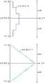
도 2는 종래 기술에 따른 화소 보상 방법을 나타내는 도면이다.2 is a diagram illustrating a pixel compensation method according to the prior art.
도 2를 참조하면, 종래 기술의 외부 보상 방법에서, 화상을 표시하는 디스플레이 구동 기간 중, 데이터 드라이버의 ADC의 레인지를 고정시켜 실시간(real time)으로 화소의 열화 정도를 센싱하고 있다.Referring to FIG. 2, in the external compensation method of the related art, the range of the ADC of the data driver is fixed during the display driving period for displaying an image, and the degree of degradation of the pixel is sensed in real time.
ADC의 레인지에 따라서 보상 데이터의 레인지가 결정되는데, 보상 데이터가 10비트로 생성되는 경우, 화소에서 센싱 된 전압 값을 총 1024 단계로 구분할 수 있다. 예로서, ACD가 ±3V의 레인지를 가지는 경우, 상기 10비트 보상 데이터는 약 2.9mV(3/1024) 단위로 보상이 이루어지도록 할 수 있다. 한편, ADC가 ±1V의 레인지를 가지는 경우, 상기 10비트 보상 데이터는 약 1.02mV(1/1024) 단위로 보상이 이루어지도록 할 수 있다.The range of the compensation data is determined according to the range of the ADC. When the compensation data is generated with 10 bits, the voltage value sensed by the pixel can be divided into 1024 steps. For example, if the ACD has a range of ± 3V, the 10-bit compensation data may be compensated in units of about 2.9 mV (3/1024). On the other hand, when the ADC has a range of ± 1 V, the 10-bit compensation data can be compensated in units of about 1.02 mV (1/1024).
보상 레인지가 넓은 경우, 화소의 보상이 빠르게 이루어지도록 할 수 있지만 이에 따라 노이즈의 영향도 증가하는 문제점이 있다. 즉, 목표로 한 보상 값에 수렴하는 시간은 줄일 수 있지만 노이즈에 민감한 특성을 가지게 된다.If the compensation range is wide, the compensation of the pixel can be performed quickly, but the influence of the noise also increases. That is, the time to converge to the target compensation value can be reduced, but the characteristic is sensitive to noise.
한편, 보상 레인지 좁은 경우, 노이즈의 영향을 줄여 목표한 보상 값에 정확하게 보상이 이루어지도록 할 수 있지만, 이에 따라 보상에 소요되는 시간이 길어지는 문제점이 있다. 즉, 목표로 한 보상 값에 근접하도록 보상이 이루어지도록 할 수 있지만, 목표한 보상 값에 수렴하기까지 장시간이 소요되는 문제점이 있다.On the other hand, when the compensation range is narrow, it is possible to reduce the influence of the noise to compensate the target compensation value accurately, but there is a problem that the time required for the compensation becomes longer. That is, although compensation can be made to approach the target compensation value, there is a problem that it takes a long time to converge to the target compensation value.
종래 기술에 따른 유기 발광 디스플레이 장치는 ACD의 레인지 값 즉, 화소의 보상 레인지를 하나의 값으로 고정하여 외부 보상을 구동함으로 인해, 보상 레인지를 넓게 한 경우에는 노이즈가 증가하여 화질이 떨어지는 문제점이 있고, 반대로 보상 레인지를 좁게 한 경우에는 보상에 소요되는 시간이 길어지는 문제점이 있다.The OLED display device according to the related art has a problem that noise is increased and image quality is deteriorated when the compensation range is widened by driving the external compensation by fixing the range value of the ACD, that is, the compensation range of the pixel to one value . On the contrary, when the compensation range is narrowed, the time required for compensation becomes long.
본 발명은 전술한 문제점을 해결하기 위한 것으로, 외부 보상을 위한 센싱 데이터의 노이즈 영향을 줄일 수 있는 유기 발광 디스플레이 장치와 이의 구동 방법을 제공하는 것을 기술적 과제로 한다.An object of the present invention is to provide an organic light emitting display device and a method of driving the same that can reduce the influence of noise of sensing data for external compensation.
본 발명은 전술한 문제점을 해결하기 위한 것으로, 외부 보상 성능을 향상시킬 수 있는 유기 발광 디스플레이 장치와 이의 구동 방법을 제공하는 것을 기술적 과제로 한다.SUMMARY OF THE INVENTION It is an object of the present invention to provide an organic light emitting display device and a driving method thereof that can improve external compensation performance.
본 발명은 전술한 문제점을 해결하기 위한 것으로, 외부 보상의 센싱 에러가 발생하는 것을 방지할 수 있는 유기 발광 디스플레이 장치와 이의 구동 방법을 제공하는 것을 기술적 과제로 한다.An object of the present invention is to provide an organic light emitting display device and a method of driving the same that can prevent a sensing error of external compensation from occurring.
위에서 언급된 본 발명의 기술적 과제 외에도, 본 발명의 다른 특징 및 이점들이 이하에서 기술되거나, 그러한 기술 및 설명으로부터 본 발명이 속하는 기술분야에서 통상의 지식을 가진 자에게 명확하게 이해될 수 있을 것이다.Other features and advantages of the invention will be set forth in the description which follows, or may be obvious to those skilled in the art from the description and the claims.
상술한 과제를 달성하기 위한 본 발명의 실시 예에 따른 유기 발광 디스플레이 장치의 구동 방법은, 디스플레이 패널에 형성된 복수의 화소를 외부 보상하는 유기 발광 디스플레이 장치의 구동 방법에 있어서, 상기 디스플레이 패널에 구성된 복수의 화소 보상 구동 시 복수의 보상 레인지를 적용하되, 상기 디스플레이 패널의 초기 구동 시점에 적용되는 보상 레인지와 상기 초기 구동 시점 이후에 적용되는 보상 레인지는 서로 상이한 것을 특징으로 한다.According to an aspect of the present invention, there is provided a method of driving an organic light emitting display device that compensates a plurality of pixels formed on a display panel by external compensation, A compensation range applied at an initial driving time point of the display panel and a compensation range applied after the initial driving time point are different from each other.
상술한 과제를 달성하기 위한 유기 발광 디스플레이 장치는, 디스플레이 패널에 형성된 복수의 화소를 외부 보상하는 유기 발광 디스플레이 장치에 있어서, 유기 발광 다이오드 및 상기 유기 발광 다이오드를 발광시키는 화소 회로로 구성된 복수의 화소를 포함하는 디스플레이 패널; 상기 복수의 화소 구동을 위한 스캔 신호, 센싱을 위한 센스 신호 및 구동 전압을 공급하는 게이트 드라이버; 화소의 보상 구동 시 시간에 따라 보상 레인지를 가변시켜 상기 화소에 충전된 전압을 센싱하고 각 화소를 보상하는 데이터 드라이버; 상기 게이트 드라이버와 상기 데이터 드라이버를 디스플레이 모드 및 센싱 모드로 동작하도록 제어하는 타이밍 컨트롤러; 및 상기 복수의 화소의 보상을 위한 보상 데이터가 저장된 메모리;를 포함하고, 상기 디스플레이 패널의 초기 구동 시점에는 제1 보상 레인지를 적용하여 화소의 보상 구동이 이루어지도록 하고, 상기 초기 구동 시점 이후, 화상의 디스플레이 구동 시에는 제2 보상 레인지를 적용하여 화상의 보상 구동이 이루어지도록 하는 것을 특징으로 한다.According to an aspect of the present invention, there is provided an organic light emitting diode (OLED) display device for external compensation of a plurality of pixels formed on a display panel, the OLED display including a plurality of pixels each including an organic light emitting diode and a pixel circuit for emitting the organic light emitting diode A display panel including the display panel; A gate driver for supplying a scan signal for driving the plurality of pixels, a sense signal for sensing, and a drive voltage; A data driver for varying a compensation range according to a time during compensation driving of the pixel to sense a voltage charged in the pixel and compensate each pixel; A timing controller for controlling the gate driver and the data driver to operate in a display mode and a sensing mode; And a memory for storing compensation data for compensation of the plurality of pixels, wherein compensation driving of a pixel is performed by applying a first compensation range at an initial driving time of the display panel, The compensation drive of the image is performed by applying the second compensation range.
본 발명의 실시 예에 따른 유기 발광 디스플레이 장치와 이의 구동 방법은 센싱 데이터의 노이즈 영향을 줄일 수 있다.The organic light emitting display device and the driving method thereof according to the embodiment of the present invention can reduce the noise influence of the sensing data.
본 발명의 실시 예에 따른 유기 발광 디스플레이 장치와 이의 구동 방법은 외부 보상 성능을 향상시킬 수 있다.The organic light emitting display device and the driving method thereof according to the embodiment of the present invention can improve the external compensation performance.
본 발명의 실시 예에 따른 유기 발광 디스플레이 장치와 이의 구동 방법은 외부 보상의 센싱 에러가 발생하는 것을 방지할 수 있다.The organic light emitting display device and the driving method thereof according to the embodiment of the present invention can prevent a sensing error of external compensation from occurring.
이 밖에도, 본 발명의 실시 예들을 통해 본 발명의 또 다른 특징 및 이점들이 새롭게 파악될 수도 있을 것이다.In addition, other features and advantages of the present invention may be newly understood through embodiments of the present invention.
도 1은 종래 기술에 따른 유기 발광 디스플레이 장치의 화소 구조를 설명하기 위한 회로도이다.
도 2는 종래 기술에 따른 화소 보상 방법을 나타내는 도면이다.
도 3은 본 발명의 실시 예에 따른 유기 발광 디스플레이 장치를 개략적으로 나타내는 도면이다.
도 4는 본 발명의 실시 예에 따른 유기 발광 디스플레이 장치의 데이터 드라이버 및 화소 구조를 나타내는 도면이다.
도 5 내지 도 8은 본 발명의 실시 예에 따른 화소 보상 방법을 설명하기 위한 도면이다.1 is a circuit diagram illustrating a pixel structure of an organic light emitting display device according to a related art.
2 is a diagram illustrating a pixel compensation method according to the prior art.
3 is a view schematically showing an organic light emitting display device according to an embodiment of the present invention.
4 is a diagram illustrating a data driver and pixel structure of an organic light emitting display device according to an embodiment of the present invention.
5 to 8 are diagrams for explaining a pixel compensation method according to an embodiment of the present invention.
본 명세서에서 각 도면의 구성요소들에 참조번호를 부가함에 있어서 동일한 구성 요소들에 한해서는 비록 다른 도면상에 표시되더라도 가능한 한 동일한 번호를 가지도록 하고 있음에 유의하여야 한다.It should be noted that, in the specification of the present invention, the same reference numerals as in the drawings denote the same elements, but they are numbered as much as possible even if they are shown in different drawings.
한편, 본 명세서에서 서술되는 용어의 의미는 다음과 같이 이해되어야 할 것이다.Meanwhile, the meaning of the terms described in the present specification should be understood as follows.
단수의 표현은 문맥상 명백하게 다르게 정의하지 않는 한 복수의 표현을 포함하는 것으로 이해되어야 하고, "제1", "제 2" 등의 용어는 하나의 구성요소를 다른 구성요소로부터 구별하기 위한 것으로, 이들 용어들에 의해 권리범위가 한정되어서는 아니 된다.The word " first, "" second," and the like, used to distinguish one element from another, are to be understood to include plural representations unless the context clearly dictates otherwise. The scope of the right should not be limited by these terms.
"포함하다" 또는 "가지다" 등의 용어는 하나 또는 그 이상의 다른 특징이나 숫자, 단계, 동작, 구성요소, 부분품 또는 이들을 조합한 것들의 존재 또는 부가 가능성을 미리 배제하지 않는 것으로 이해되어야 한다.It should be understood that the terms "comprises" or "having" does not preclude the presence or addition of one or more other features, integers, steps, operations, elements, components, or combinations thereof.
"적어도 하나"의 용어는 하나 이상의 관련 항목으로부터 제시 가능한 모든 조합을 포함하는 것으로 이해되어야 한다. 예를 들어, "제1 항목, 제 2 항목 및 제 3 항목 중에서 적어도 하나"의 의미는 제1 항목, 제 2 항목 또는 제 3 항목 각각 뿐만 아니라 제1 항목, 제 2 항목 및 제 3 항목 중에서 2개 이상으로부터 제시될 수 있는 모든 항목의 조합을 의미한다.It should be understood that the term "at least one" includes all possible combinations from one or more related items. For example, the meaning of "at least one of the first item, the second item and the third item" means not only the first item, the second item or the third item, but also the second item and the second item among the first item, Means any combination of items that can be presented from more than one.
이하, 본 발명에 따른 유기 발광 디스플레이 장치와 이의 구동 방법의 바람직한 실시 예를 첨부된 도면을 참조하여 상세히 설명한다.Hereinafter, preferred embodiments of the organic light emitting display device and the driving method thereof according to the present invention will be described in detail with reference to the accompanying drawings.
도 3은 본 발명의 실시 예에 따른 유기 발광 디스플레이 장치를 개략적으로 나타내는 도면이고, 도 4는 본 발명의 실시 예에 따른 유기 발광 디스플레이 장치의 데이터 드라이버 및 화소 구조를 나타내는 도면이다.FIG. 3 is a schematic view of an organic light emitting display device according to an embodiment of the present invention, and FIG. 4 is a diagram illustrating a data driver and pixel structure of an organic light emitting display device according to an embodiment of the present invention.
도 3 및 도 4를 참조하면, 본 발명의 실시 예에 따른 유기 발광 디스플레이 장치는 디스플레이 패널(100) 및 패널 구동부를 포함하여 구성된다.3 and 4, the organic light emitting display device according to the embodiment of the present invention includes a
상기 디스플레이 패널(100)은 복수의 게이트 라인(GL), 복수의 센싱 신호 라인(SL), 복수의 데이터 라인(DL), 복수의 구동 전원 라인(PL), 복수의 기준 전원 라인(RL) 및 복수의 화소(P)를 포함한다.The
복수의 화소(P)는 제1 구동 전원(VDD)이 공급되는 드라이빙 TFT(DT)의 게이트 전극과 소스 전극 간에 접속된 커패시터(Cst)에 데이터 전압(Vdata)과 기준 전압(Vref)의 차 전압(Vdata-Vref)을 충전하고, 커패시터(Cst)의 충전 전압에 따라 제1 구동 전원(VDD)으로부터 드라이빙 TFT(DT)를 통해 제2 구동 전원(VSS)으로 흐르는 데이터 전류(Ioled)로 유기 발광 다이오드(OLED)를 발광시킨다.The plurality of pixels P are connected to the capacitor Cst connected between the gate electrode and the source electrode of the driving TFT DT to which the first driving power supply VDD is supplied with the difference voltage Vdata between the data voltage Vdata and the reference voltage Vref And the data current Ioled flowing from the first driving power supply VDD to the second driving power supply VSS via the driving TFT DT is charged with the organic light emission (Vdata-Vref) according to the charging voltage of the capacitor Cst. Thereby causing the diode OLED to emit light.
상기 복수의 화소(P) 각각은 적색 화소, 녹색 화소, 청색 화소, 및 백색 화소 중 어느 하나로 이루어질 수 있다. 하나의 영상을 표시하는 하나의 단위 화소는 인접한 적색 화소, 녹색 화소, 및 청색 화소로 이루어지거나, 인접한 적색 화소, 녹색 화소, 청색 화소, 및 백색 화소로 이루어질 수 있다.Each of the plurality of pixels P may be any one of a red pixel, a green pixel, a blue pixel, and a white pixel. One unit pixel for displaying one image may be composed of adjacent red pixels, green pixels, and blue pixels, or may be composed of adjacent red pixels, green pixels, blue pixels, and white pixels.
상기 복수의 화소(P) 각각은 디스플레이 패널(100)에 정의된 화소 영역에 형성된다. 이를 위해, 상기 디스플레이 패널(100)은 상기 화소 영역을 정의하도록 상기 복수의 게이트 라인(GL), 복수의 센싱 신호 라인(SL), 복수의 데이터 라인(DL), 복수의 구동 전원 라인(PL) 및 복수의 기준 전원 라인(RL)이 형성되어 있다.Each of the plurality of pixels P is formed in a pixel region defined in the
상기 복수의 게이트 라인(GL)과 복수의 센싱 신호 라인(SL)은 디스플레이 패널(100) 내에서 제1 방향(예로서, 수평 방향)으로 나란히 형성될 수 있다. 이때, 게이트 라인(GL)에는 패널 구동부의 게이트 드라이버(300)로부터 스캔 신호(scan, 게이트 구동 신호)가 인가되고, 센싱 신호 라인(SL)에는 센싱 신호(sense)가 인가된다.The plurality of gate lines GL and the plurality of sensing signal lines SL may be formed in parallel in the first direction (e.g., the horizontal direction) in the
상기 복수의 데이터 라인(DL)은 상기 복수의 게이트 라인(GL) 및 복수의 센싱 신호 라인(SL)과 교차하도록 제2 방향(예로서, 수직 방향)으로 형성될 수 있다. 이때, 데이터 라인(DL)에는 패널 구동부의 데이터 드라이버(200)로부터 데이터 전압(Vdata)이 공급된다. 데이터 전압(Vdata)은 해당 화소(P)의 드라이빙 TFT(DT)의 문턱 전압에 대응되는 보상 전압이 부가된 전압 레벨을 가지며, 상기 보상 전압에 대해서는 후술하기로 한다.The plurality of data lines DL may be formed in a second direction (e.g., a vertical direction) so as to intersect the plurality of gate lines GL and the plurality of sensing signal lines SL. At this time, the data voltage Vdata is supplied from the
상기 복수의 기준 전압 라인(RL)은 상기 복수의 데이터 라인(DL) 각각과 나란하게 형성된다. 이러한, 기준 전압 라인(RL)에는 상기 패널 구동부로부터 기준 전압(Vref) 또는 프리차징 전압(Vpre)이 선택적으로 공급될 수 있다. 이때, 상기 기준 전압(Vref)은 각 화소(P)의 데이터 충전 기간 동안 각 기준 전압 라인(RL)에 공급되며, 상기 프리차징 전압(Vpre)은 각 화소(P)의 드라이빙 TFT(DT)의 문턱 전압/이동도를 검출하는 검출 기간에 기준 전압 라인(RL)에 공급될 수 있다.The plurality of reference voltage lines RL are formed in parallel with the plurality of data lines DL. The reference voltage line RL may be selectively supplied with the reference voltage Vref or the precharging voltage Vpre from the panel driver. At this time, the reference voltage Vref is supplied to each reference voltage line RL during the data charging period of each pixel P, and the precharging voltage Vpre is supplied to the driving TFT DT of each pixel P And may be supplied to the reference voltage line RL in the detection period for detecting the threshold voltage / mobility.
상기 복수의 구동 전원 라인(PL)은 상기 게이트 라인(GL)과 나란하게 형성될 수 있으며, 제1 구동 전원(VDD)을 화소(P)에 공급한다.The plurality of driving power supply lines PL may be formed in parallel with the gate lines GL and supply the first driving power VDD to the pixels P. [
도 4에 도시된 바와 같이, 복수의 화소(P) 각각은 데이터 충전 기간 동안에 데이터 전압(Vdata)과 기준 전압(Vref)의 차 전압(Vdata-Vref)을 상기 커패시터(Cst)에 충전하고, 상기 발광 기간 동안 커패시터(Cst)의 충전 전압에 따라 데이터 전류(Ioled)를 유기 발광 다이오드(OLED)에 공급하는 화소 회로(PC)를 포함한다.4, each of the plurality of pixels P charges the capacitor Cst with a difference voltage Vdata-Vref between the data voltage Vdata and the reference voltage Vref during a data charging period, And a pixel circuit PC for supplying the data current Ioled to the organic light emitting diode OLED according to the charging voltage of the capacitor Cst during the light emission period.
각 화소(P)의 화소 회로(PC)는 제1 스위칭 TFT(ST1), 제2 스위칭 TFT(ST2), 상기 드라이빙 TFT(DT), 및 커패시터(Cst)를 포함하여 구성된다. 여기서, 상기 TFT들(ST1, ST2, DT)은 N형 TFT로서 a-Si TFT, poly-Si TFT, Oxide TFT, Organic TFT 등이 될 수 있다. 그러나, 이에 한정되지 않고, 상기 TFT들(ST1, ST2, DT)은 P형 TFT로 형성될 수도 있다.The pixel circuit PC of each pixel P includes a first switching TFT ST1, a second switching TFT ST2, the driving TFT DT, and a capacitor Cst. Here, the TFTs ST1, ST2, and DT may be an a-Si TFT, a poly-Si TFT, an oxide TFT, an organic TFT, or the like as an N-type TFT. However, the present invention is not limited to this, and the TFTs ST1, ST2, and DT may be formed of a P-type TFT.
상기 제1 스위칭 TFT(ST1)는 게이트 라인(GL)에 접속된 게이트 전극, 데이터 라인(DL)에 접속된 소스 전극(제1 전극), 및 드라이빙 TFT(DT)의 게이트 전극과 연결된 제1 노드(n1)에 접속된 드레인 전극(제2 전극)을 포함한다. 이러한, 제1 스위칭 TFT(ST1)는 게이트 라인(GL)에 공급되는 게이트 온 전압 레벨의 스캔 신호에 따라 턴-온(turn-on)되어, 데이터 라인(DL)에 공급되는 데이터 전압(Vdata)을 제1 노드(n1) 즉, 드라이빙 TFT(DT)의 게이트 전극에 공급한다.The first switching TFT ST1 includes a gate electrode connected to the gate line GL, a source electrode connected to the data line DL (first electrode), and a first node connected to the gate electrode of the driving TFT DT (second electrode) connected to the drain electrode n1. The first switching TFT ST1 is turned on according to a scan signal having a gate-on voltage level supplied to the gate line GL and is supplied with the data voltage Vdata supplied to the data line DL. To the first node n1, that is, the gate electrode of the driving TFT DT.
상기 제2 스위칭 TFT(ST2)는 센싱 신호 라인(SL)에 접속된 게이트 전극, 기준 전압 라인(RL)에 접속된 소스 전극(제1 전극) 및 드라이빙 TFT(DT)과 유기 발광 다이오드(OLED)가 연결된 제2 노드(n2)에 접속된 드레인 전극(제2 전극)을 포함한다. 이러한, 상기 제2 스위칭 TFT(ST2)는 상기 센싱 신호 라인(SL)에 공급되는 게이트 온 전압 레벨의 센싱 신호(sense)에 따라 턴-온(turn-on)되어, 기준 전압 라인(RL)에 공급되는 기준 전압(Vref, 또는 프리차징 전압)을 드라이빙 TFT(DT)의 드레인 전극에 공급한다.The second switching TFT ST2 includes a gate electrode connected to the sensing signal line SL, a source electrode (first electrode) connected to the reference voltage line RL and the driving TFT DT and the organic light emitting diode OLED. And a drain electrode (second electrode) connected to a second node n2 connected to the second node n2. The second switching TFT ST2 is turned on according to a sensing signal sense of a gate-on voltage level supplied to the sensing signal line SL and is supplied to the reference voltage line RL And supplies the supplied reference voltage Vref or precharged voltage to the drain electrode of the driving TFT DT.
상기 커패시터(Cst)는 상기 드라이빙 TFT(DT)의 게이트 전극과 드레인 전극, 즉, 상기 제1 노드(n1) 및 제2 노드(n2) 사이에 접속되어 있다. 이러한, 커패시터(Cst)는 제1 노드(n1) 및 제2 노드(n2) 각각에 공급되는 전압의 차 전압을 충전한 후, 충전된 전압에 따라 상기 드라이빙 TFT(DT)를 스위칭시킨다.The capacitor Cst is connected between the gate electrode and the drain electrode of the driving TFT DT, that is, between the first node n1 and the second node n2. The capacitor Cst charges the difference voltage between the voltages supplied to the first node n1 and the second node n2, and then switches the driving TFT DT according to the charged voltage.
상기 드라이빙 TFT(DT)는 상기 제1 스위칭 TFT(ST1)의 드레인 전극과 상기 커패시터(Cst)의 제1 전극에 공통으로 접속된 게이트 전극을 포함한다. 그리고, 상기 드라이빙 TFT(DT)는 상기 구동 전원 라인(PL)에 접속된 소스 전극을 포함한다. 또한, 상기 드라이빙 TFT(DT)는 상기 제2 스위칭 TFT(ST2)의 드레인 전극과 상기 커패시터(Cst)의 제2 전극 및 상기 유기 발광 다이오드(OLED)의 애노드에 공통으로 접속된 드레인 전극을 포함한다.The driving TFT DT includes a gate electrode commonly connected to a drain electrode of the first switching TFT (ST1) and a first electrode of the capacitor (Cst). The driving TFT DT includes a source electrode connected to the driving power supply line PL. The driving TFT DT includes a drain electrode of the second switching TFT ST2, a second electrode of the capacitor Cst, and a drain electrode commonly connected to an anode of the organic light emitting diode OLED .
이러한, 상기 드라이빙 TFT(DT)는 발광 기간마다 상기 커패시터(Cst)의 전압에 의해 턴-온됨으로써 제1 구동 전원(VDD)에 의해 유기 발광 다이오드(OLED)로 흐르는 전류 량을 제어한다.The driving TFT DT controls the amount of current flowing to the organic light emitting diode OLED by the first driving power supply VDD by being turned on by the voltage of the capacitor Cst every light emitting period.
상기 유기 발광 다이오드(OLED)는 상기 화소 회로(PC), 즉 드라이빙 TFT(DT)로부터 공급되는 데이터 전류(Ioled)에 의해 발광하여 데이터 전류(Ioled)에 대응되는 휘도를 가지는 단색 광을 방출한다.The organic light emitting diode OLED emits monochromatic light having a luminance corresponding to the data current Ioled by the data current Ioled supplied from the pixel circuit PC, i.e., the driving TFT DT.
이를 위해, 상기 유기 발광 다이오드(OLED)는 화소 회로(PC)의 제2 노드(n2)에 접속된 애노드 전극(미도시), 애노드 전극 상에 형성된 유기층(미도시), 및 유기층 상에 형성되어 제2 구동 전원(VSS)이 공급되는 캐소드 전극(미도시)을 포함한다.The organic light emitting diode OLED includes an anode electrode (not shown) connected to the second node n2 of the pixel circuit PC, an organic layer (not shown) formed on the anode electrode, and an organic layer And a cathode electrode (not shown) to which the second driving power supply VSS is supplied.
유기층은 정공 수송층/유기 발광층/전자 수송층의 구조 또는 정공 주입층/정공 수송층/유기 발광층/전자 수송층/전자 주입층의 구조를 가지도록 형성될 수 있다. 나아가, 상기 유기층은 상기 유기 발광층의 발광 효율 및/또는 수명 등을 향상시키기 위한 기능층을 더 포함하여 이루어질 수 있다. 이때, 상기 제2 구동 전원(VSS)은 라인 형태로 형성된 제2 구동 전원 라인(미도시)을 통해 상기 유기 발광 다이오드(OLED)의 캐소드 전극에 공급될 수 있다.The organic layer may have a structure of a hole transporting layer / an organic light emitting layer / an electron transporting layer or a structure of a hole injecting layer / a hole transporting layer / an organic light emitting layer / an electron transporting layer / an electron injecting layer. Further, the organic layer may further include a functional layer for improving the luminous efficiency and / or lifetime of the organic light emitting layer. At this time, the second driving power source VSS may be supplied to the cathode electrode of the organic light emitting diode OLED through a second driving power line (not shown) formed in a line shape.
상기 패널 구동부는 데이터 드라이버(200), 게이트 드라이버(300), 타이밍 컨트롤러(400) 및 결함 화소 데이터 및 보상 데이터가 저장되는 메모리(500)를 포함하여 구성된다.The panel driver includes a
상기 게이트 드라이버(300)는 복수의 게이트 라인(GL) 및 복수의 센싱 신호 라인(SL)과 연결되어 타이밍 컨트롤러(400)의 제어에 따라 상기 디스플레이 모드와 상기 센싱 모드로 동작한다.The
상기 디스플레이 모드 시, 상기 게이트 드라이버(300)는 각 화소(P)의 데이터 충전 기간마다 게이트 온 전압 레벨의 스캔 신호를 복수의 게이트 라인(GL1~GLm)에 순차적으로 공급함과 동시에, 제1 전압 레벨의 제1 구동 전원(VDD)을 복수의 제1 구동 전원 라인(PL1 내지 PLm)에 공급한다.In the display mode, the
또한, 상기 게이트 드라이버(300)는 각 화소(P)의 발광 기간마다 상기 스캔 신호를 게이트 오프 전압 레벨로 낮추고, 제1 전압 레벨과 다른 제 2 전압 레벨의 제1 구동 전원(VDD)을 제1 구동 전원 라인(PL1 내지 PLm)에 공급한다. 이때, 상기 제1 전압 레벨은 상기 제 2 전압 레벨보다 낮은 전압 레벨을 가지거나, 상기 기준 전압(Vref)과 같거나 낮은 전압 레벨을 갖는다.The
한편, 상기 디스플레이 모드 시, 상기 게이트 드라이버(300)는 각 화소(P)의 데이터 충전 기간 동안 해당하는 제1 구동 전원 라인(PL1 내지 PLm)을 플로팅(Floating)시킬 수도 있다.Meanwhile, in the display mode, the
상기 센싱 모드 시, 상기 게이트 드라이버(300)는 각 화소(P)의 초기화 기간 및 검출 전압 충전 기간마다 게이트 온 전압 레벨의 스캔 신호를 복수의 게이트 라인에 공급함과 동시에, 제1 전압 레벨의 제1 구동 전원(VDD)을 제1 구동 전원 라인(1PL1 내지 1PLm)에 공급한다.In the sensing mode, the
또한, 상기 게이트 드라이버(300)는 각 화소(P)의 전압 센싱 기간마다 게이트 온 전압 레벨의 센싱 신호(sense)를 센싱 신호 라인(SL)에 공급함과 동시에, 제 2 전압 레벨의 제1 구동 전원(VDD)을 제1 구동 전원 라인(PL1 내지 PLm)에 공급한다.The
한편, 상기 센싱 모드 시, 상기 게이트 드라이버(300)는 각 화소(P)의 초기화 기간 동안 해당하는 제1 구동 전원 라인(1PL1 내지 1PLm)을 플로팅(Floating)시킬 수도 있다.Meanwhile, in the sensing mode, the
상기 타이밍 컨트롤러(400)는 상기 데이터 드라이버(200)와 상기 게이트 드라이버(300) 각각을 상기 디스플레이 모드로 동작시키고, 사용자의 설정 또는 설정된 드라이빙 TFT의 문턱 전압/이동도 검출 시점에서는 상기 데이터 드라이버(200)와 상기 게이트 드라이버(300) 각각을 상기 센싱 모드로 동작시킨다.The
상기 센싱 모드는 디스플레이 패널(100)이 제조된 후, 제품으로 출하되기 전에 수행될 수 있다. 또한, 상기 센싱 모드는 제품으로 출시된 이후, 디스플레이 패널(100)의 초기 구동시점에 수행될 수 있다. 또한, 상기 센싱 모드는 디스플레이 패널(100)의 장시간 구동 이후 종료시점에 수행될 수 있다. 그리고, 상기 센싱 모드는 디스플레이 패널(100)에 영상을 표시하는 프레임의 블랭크 기간에서 수행될 수 있다.The sensing mode may be performed after the
디스플레이 패널(100)이 제조된 후, 제품으로 출하되기 전에 디스플레이 패널(100)의 전체 화소를 센싱하고, 센싱 결과에 따라 전체 화소의 보상 데이터를 생성하고, 생성된 보상 데이터를 메모리(500)에 저장해 놓을 수 있다.After the
디스플레이 패널(100)의 초기 구동시점 또는 장시간 구동 이후 종료시점의 센싱 모드에서, 상기 타이밍 컨트롤러(400)는 한 프레임 동안 디스플레이 패널(100)의 모든 화소(P)의 드라이빙 TFT(DT)의 문턱 전압/이동도를 검출한다.The
상기 블랭크 기간의 센싱 모드에서, 상기 타이밍 컨트롤러(400)는 상기 블랭크 기간마다 1개의 수평 라인에 형성된 화소(P)의 드라이빙 TFT(DT)의 문턱 전압/이동도를 검출할 수 있다.In the sensing mode of the blank period, the
이러한, 방식으로 상기 타이밍 컨트롤러(400)는 복수 프레임의 블랭크 기간에 걸쳐 디스플레이 패널(100)의 모든 화소(P)의 드라이빙 TFT(DT)의 문턱 전압/이동도를 검출할 수 있다.In this manner, the
상기 센싱 모드 시, 상기 타이밍 컨트롤러(400)는 상기 타이밍 동기 신호(TSS)에 기초하여 1 수평 기간 단위로 상기 각 게이트 라인 그룹(G1 내지 Gm)에 접속된 각 화소(P)의 드라이빙 TFT(DT)의 문턱 전압/이동도를 검출하기 위한 데이터 제어 신호(DCS), 게이트 제어 신호(GCS) 및 전원 제어 신호(PCS)를 생성하고, 이를 이용해 상기 데이터 드라이버(200)와 상기 게이트 드라이버(300) 각각의 구동을 센싱 모드로 제어한다.In the sensing mode, the
상기 타이밍 동기 신호(TSS)는 수직 동기 신호(Vsync), 수평 동기 신호(Hsync), 데이터 인에이블(DE), 클럭(DCLK) 등이 될 수 있다. 상기 게이트 제어 신호(GCS)는 게이트 스타트 신호, 및 복수의 클럭 신호 등으로 이루어질 수 있다. 데이터 제어 신호(DCS)는 데이터 스타트 신호, 데이터 쉬프트 신호, 및 데이터 출력 신호 등으로 이루어질 수 있다. 그리고, 상기 전원 제어 신호(PCS)는 전원 스타트 신호, 및 전원 쉬프트 신호 등으로 이루어질 수 있다.The timing synchronization signal TSS may be a vertical synchronization signal Vsync, a horizontal synchronization signal Hsync, a data enable DE, a clock DCLK, or the like. The gate control signal GCS may be a gate start signal, a plurality of clock signals, or the like. The data control signal DCS may be a data start signal, a data shift signal, a data output signal, or the like. The power control signal PCS may be a power start signal, a power supply shift signal, or the like.
상기 센싱 모드 시, 상기 타이밍 컨트롤러(400)는 설정된 검출용 데이터를 생성하여 상기 데이터 드라이버(200)에 공급한다.In the sensing mode, the
상기 디스플레이 모드 시, 상기 타이밍 컨트롤러(400)는 상기 센싱 모드에 의해 상기 데이터 드라이버(200)로부터 제공된 각 화소(P)의 센싱 데이터(sensing data)에 기초하여 외부로부터 입력되는 입력 데이터(Idata)를 보정하여 화소 데이터(DATA)를 생성한다.In the display mode, the
그리고, 생성된 화소 데이터(DATA)를 디스플레이 패널(100)에 형성된 각 데이터 라인(DL)에 공급한다. 이때, 상기 각 화소(P)에 공급될 화소 데이터(DATA)는 각 화소(P)의 드라이빙 TFT(DT)의 문턱 전압/이동도를 보상하기 위한 보상 전압이 반영된 전압 레벨을 갖는다.The generated pixel data (DATA) is supplied to each data line (DL) formed on the display panel (100). The pixel data DATA to be supplied to each pixel P has a voltage level at which a compensation voltage for compensating the threshold voltage / mobility of the driving TFT DT of each pixel P is reflected.
상기 입력 데이터(Idata)는 하나의 단위 화소에 공급될 적색, 녹색, 및 청색의 입력 데이터로 이루어질 수 있다. 그리고, 상기 단위 화소가 적색 화소, 녹색 화소, 및 청색 화소로 이루어진 경우, 하나의 화소 데이터(DATA)는 적색, 녹색, 또는 청색의 데이터일 수 있다.The input data Idata may be input data of red, green, and blue to be supplied to one unit pixel. When the unit pixel is composed of a red pixel, a green pixel, and a blue pixel, one pixel data (DATA) may be red, green, or blue data.
반면에, 상기 단위 화소가 적색 화소, 녹색 화소, 청색 화소 및 백색 화소로 이루어진 경우, 하나의 화소 데이터(DATA)는 적색, 녹색, 청색, 또는 백색의 데이터일 수 있다.On the other hand, when the unit pixel is composed of a red pixel, a green pixel, a blue pixel and a white pixel, one pixel data (DATA) may be data of red, green, blue or white.
메모리(500)에는 디스플레이 패널(100)의 화소(P) 각각에 대한 보상 데이터가 화소 배치 구조에 대응되도록 맵핑되어 있다.In the
상기 센싱 모드에 따라 상기 데이터 드라이버(200)에 의해 검출된 화소(P) 각각에 대한 초기 검출 데이터가 화소 배치 구조에 대응되도록 메모리(500)에 맵핑되어 있다. 상기 초기 검출 데이터는 디스플레이 패널(100)의 출하 시점 또는 초기 구동시점에 전술한 센싱 모드의 수행을 통해 검출된 디스플레이 패널(100)의 모든 화소(P)에 대한 드라이빙 TFT(DT)의 문턱 전압/이동도에 대응되는 전압 값이 될 수 있다.The initial detection data for each of the pixels P detected by the
데이터 드라이버(200)는 복수의 데이터 라인(D1 내지 Dn)에 연결되어 타이밍 컨트롤러(400)의 모드 제어에 따라 디스플레이 모드와 센싱 모드로 동작한다. 디스플레이 모드는 각 화소에 데이터 전압을 충전시키는 데이터 충전 기간 및 유기 발광 다이오드(OLED)를 발광시키는 발광 기산으로 구동할 수 있다. 그리고, 상기 센싱 모드는 각 화소를 초기화 시키는 초기화 기간, 센싱 전압 충전 기간 및 센싱 기간으로 구동할 수 있다.The
디스플레이 모드 시, 상기 데이터 드라이버(200)는 상기 각 화소(P)의 데이터 충전 기간마다 상기 기준 전압(Vref)을 상기 기준 전압 라인(RL)에 공급함과 동시에, 상기 타이밍 컨트롤러(400)로부터 공급되는 화소 데이터(DATA)를 데이터 전압(Vdata)으로 변환하여 해당 데이터 라인(D1 내지 Dn)에 공급한다.In the display mode, the
상기 센싱 모드 시, 상기 데이터 드라이버(200)는 별도의 검출 기간마다 프리차징 전압(Vpre)을 상기 기준 전압 라인(RL)에 공급함과 동시에, 상기 타이밍 컨트롤러(400)로부터 공급되는 검출용 화소 데이터(DATA)를 검출용 데이터 전압(Vdata)으로 변환하여 해당 데이터 라인(D1 내지 Dn)에 공급한다.In the sensing mode, the
이후, 상기 프리차징 전압(Vpre)과 상기 검출용 데이터 전압(Vdata)에 의해 각 화소(P)의 드라이빙 TFT(DT)에 흐르는 전류에 대응되는 전압이 각 기준 전압 라인(RL)에 충전되도록 상기 각 기준 전압 라인(RL)을 플로팅(floating)시킨 다음, 센싱부(230)를 통해 상기 각 기준 전압 라인(RL)에 충전된 전압을 검출한다. 그리고, 검출된 전압을 각 화소(P)의 드라이빙 TFT(DT)의 문턱 전압/이동도에 대응되는 센싱 데이터(sensing data)로 변환하여 타이밍 컨트롤러(400)에 제공한다.Thereafter, the voltage corresponding to the current flowing through the driving TFT DT of each pixel P is charged in each reference voltage line RL by the precharging voltage Vpre and the detecting data voltage Vdata, The reference voltage line RL is floated and the voltage charged in the reference voltage line RL is detected through the
이를 위해, 상기 데이터 드라이버(200)는 도 4에 도시된 바와 같이, 데이터 전압 생성부(210), 기준 전압(Vref) 생성부(220), 센싱부(230) 및 스위칭부(240)를 포함하여 구성된다.4, the
상기 데이터 전압 생성부(210)는 입력되는 상기 화소 데이터(DATA)를 데이터 전압(Vdata)으로 변환하여 데이터 라인(DL)에 공급한다. 이를 위해, 상기 데이터 전압 생성부(210)는 샘플링 신호를 생성하는 쉬프트 레지스터, 샘플링 신호에 따라 화소 데이터(DATA)를 래치하는 래치부, 복수의 기준 감마 전압을 이용하여 복수의 계조 전압을 생성하는 계조 전압 생성부, 복수의 계조 전압 중에서 래치된 화소 데이터(DATA)에 대응되는 계조 전압을 데이터 전압(Vdata)으로 선택하여 출력하는 디지털-아날로그 변환부(DAC), 및 상기 데이터 전압(Vdata)을 출력하는 출력부를 포함하여 구성될 수 있다.The
상기 기준 전압 생성부(220)는 상기 프리차징 전압(Vpre) 및 상기 기준 전압(Vref)을 생성하고, 생성된 상기 프리차징 전압(Vpre) 및 상기 기준 전압(Vref)을 스위칭부(240)를 통해 각 화소에 공급한다.The
상기 스위칭부(240)는 상기 기준 전압(Vref) 또는 상기 프리차징 전압(Vpre)을 기준 전압 라인(RL)에 공급하고, 기준 전압 라인(RL)을 플로팅 시킨 후 센싱부(230)에 접속시킨다. 또한, 센싱부(230)를 구성하는 복수의 센싱 블록(230a, 230b) 중 하나의 센싱부가 기준 전압 라인(RL)에 충전된 전압을 검출할 수 있도록 스위칭 한다.The
구체적으로, 상기 스위칭부(240)는 상기 디스플레이 모드에 따른 타이밍 컨트롤러(400)의 제어에 따라 기준 전압(Vref)을 기준 전압 라인(RL)에 공급한다. 반면에, 상기 스위칭부(240)는 상기 센싱 모드에 따른 타이밍 컨트롤러(400)의 제어에 따라 프리차징 전압(Vpre)을 기준 전압 라인(RL)에 공급한 다음, 기준 전압 라인(RL)을 플로팅 시킨다. 이후, 기준 전압 라인(RL)을 센싱부(230)에 접속시킨다.Specifically, the
상기 센싱부(230)는 센싱 블록(230a, 230b)을 포함하며, 제1 센싱 블록(230a)과 제2 센싱 블록(230b)은 상이한 레인지를 가지는 ADC로 구성될 수 있다. 예로서, 제1 센싱 블록(230a)은 ±3V의 레인지를 가질 수 있고, 제2 센싱 블록(230b)은 ±1V의 레인지를 가질 수 있다.The
상기 센싱부(230)를 구성하는 복수의 센싱 블록(230a, 230b) 중 하나의 센싱 블록이 상기 스위칭부(240)의 스위칭에 의해 기준 전압 라인(RL)에 접속되어 상기 기준 전압 라인(RL)에 충전된 전압을 검출한다.One sensing block of the plurality of
제1 센싱 블록(230a)과 제2 센싱 블록(230b) 중에서, 상기 스위칭부(240)에 의해 제1 센싱 블록(230a)이 선택되면, ±3V의 레인지로 보상 데이터가 생성되어 화소의 보상이 빠르게 이루어지도록 할 수 있다. 즉, 목표 보상 값에 수렴하는 시간을 줄일 수 있다.When the
한편, 제1 센싱 블록(230a)과 제2 센싱 블록(230b) 중에서, 상기 스위칭부(240)에 의해 제2 센싱 블록(230b)이 선택되면, ±1V의 레인지로 보상 데이터가 생성되어 목표 보상 값에 근접하게 보상이 이루어지도록 할 수 있다. 즉, 목표 보상 값에 보다 근접한 값으로 상이 이루어지도록 할 수 있다.Meanwhile, if the
디스플레이 패널(100)의 초기 구동 시점에서는 ±3V의 레인지로 화소의 보상 구동이 이루어지도록 하고, 이후 디스플레이 구동 시점에서는 ±1V의 레인지로 화소의 보상 구동이 이루어지도록 할 수 있다. 또한, 초기 구동 시점 이후, 시간 경과에 따라서 보상 레인지를 감소시켜 화소의 보상 구동이 이루어지도록 할 수 있다.It is possible to compensate and drive the pixel with a range of ± 3 V at the initial driving time of the
상기 센싱부(230)를 구성하는 복수의 센싱 블록(230a, 230b)은 검출된 전압에 대응되는 디지털 형태의 센싱 데이터(sensing data)를 생성하여 타이밍 컨트롤러(400)에 제공한다.The plurality of
상기 기준 전압 라인(RL)으로부터 검출된 전압은, 시간 변화에 따라서 드라이빙 TFT(DT)에 흐르는 전류와 기준 전압 라인(RL)의 정전 용량의 비율로 결정될 수 있다. 이때, 상기 센싱 데이터(sensing data)는 각 화소(P)의 드라이빙 TFT(DT)에 대한 문턱 전압/이동도에 대응되는 데이터로 이루어진다.The voltage detected from the reference voltage line RL can be determined by the ratio of the current flowing in the driving TFT DT to the capacitance of the reference voltage line RL with time change. At this time, the sensing data is composed of data corresponding to the threshold voltage / mobility of each pixel P with respect to the driving TFT DT.
여기서, 사용자가 유기 발광 디스플레이 장치의 전원을 온(on) 시키면, 화상이 디스플레이 되기 전까지 대략 1~2초 가량의 소요된다. 이러한, 화상의 디스플레이 구동이 시작되는 초기 구동 시점에 디스플레이 패널(100)의 전체 화소에 대해서 센싱 구동이 이루어지고, 초기 구동 시점의 센싱 결과에 기초하여 전체 화소를 보상하게 된다.Here, when the user turns on the power of the organic light emitting display device, it takes about 1 to 2 seconds until the image is displayed. At the initial driving timing at which the display driving of the image is started, all the pixels of the
본 발명의 실시 예에 따른 유기 발광 디스플레이 장치는 이러한, 초기 구동 시점의 외부 보상 구동 시, 노이즈에 의한 센싱 에러를 줄여 화질 저하를 방지하면서, 목표 보상 값으로 빠르게 전체 화소가 보상 되도록 한다.The organic light emitting display device according to the embodiment of the present invention can reduce the sensing error due to the noise during the external compensation driving at the initial driving time so as to prevent degradation of the image quality and quickly compensate the entire pixels with the target compensation value.
도 5 내지 도 8은 본 발명의 실시 예에 따른 화소 보상 방법을 설명하기 위한 도면이다.5 to 8 are diagrams for explaining a pixel compensation method according to an embodiment of the present invention.
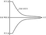
도 5에 도시된 바와 같이, 보상 레인지가 큰 경우, 화소의 보상을 빠르게 수행할 수 있는 반면, 레인지 보다 작은 노이즈도 센싱하게 되고, 노이즈가 보상에 반영되므로 노이즈에 다소 취약한 특성을 가질 수 있다.As shown in FIG. 5, when the compensation range is large, the compensation of the pixel can be performed quickly, while the noise smaller than the range is sensed, and the noise is reflected in the compensation, so that the characteristic can be somewhat vulnerable to noise.
한편, 도 6에 도시된 바와 같이, 보상 레인지가 작은 경우, 일정 크기의 노이즈를 필터링 할 수 있어 노이즈에 강하고, 각 화소의 보상 값이 보상 목표 값에 정확하게 수렴하도록 할 수 있는 반면, 화소의 보상에 시간이 많이 소요될 수 있다.On the other hand, as shown in FIG. 6, when the compensation range is small, it is possible to filter the noise of a predetermined size, so that it is resistant to noise, and the compensation value of each pixel can be accurately converged to the compensation target value, Can take a lot of time.
본 발명에서는 이러한, 큰 보상 레인지와 작은 보상 레인지의 적용에 따른 장점을 이용하여 화소의 보상이 이루어지도록 한다.In the present invention, compensation of a pixel is performed by taking advantage of the advantages of applying a large compensation range and a small compensation range.
도 7 및 도 8을 참조하면, 유기 발광 디스플레이 장치가 파워 온(on)된 후, 사용 시간이 지속되면 드라이빙 TFT가 열화되어 초기 특성과 차이가 생긴다. 드라이빙 TFT의 열화를 그대로 방치하면 화상의 품질이 떨어지므로, 각 화소의 드라이빙 TFT가 열화된 정도에 따라서 외부 보상을 수행하여 각 화소를 초기 상태로 만들어 준다.Referring to FIGS. 7 and 8, when the organic light emitting display device is turned on, the driving TFT is deteriorated and the difference from the initial characteristics occurs. If the deterioration of the driving TFT is left unchanged, the quality of the image is deteriorated. Therefore, external compensation is performed according to the degree of deterioration of the driving TFT of each pixel, thereby making each pixel into an initial state.
여기서, 초기 구동 시점에는 상기 센싱부(230)를 구성하는 복수의 센싱 블록(230a, 230b) 중에서 큰 레인지를 가지는 제1 센싱 블록(230a)을 이용하여 각 화소를 센싱하고, 상기 센싱 결과 기초하여 큰 레인지로 전체 화소를 보상한다. 이를 통해, 각 화소의 보상 값이 목표 보상 값으로 수렴하는 시간을 단축시킬 수 있다.At the initial driving time, each pixel is sensed using a
이후, 각 화소의 보상 값이 목표 보상 값에 수렴된 이후에는 상기 센싱부(230)를 구성하는 복수의 센싱 블록(230a, 230b) 중에서 작은 레인지를 가지는 제2 센싱 블록(230b)을 이용하여 각 화소를 센싱하고, 상기 센싱 결과 기초하여 작은 레인지로 전체 화소를 보상한다. 이를 통해, 각 화소의 보상 값이 목표 보상 값으로 정확이 수렴되도록 하여 보상 에러를 줄일 수 있다.After the compensation value of each pixel is converged to the target compensation value, the
이와 같이, 화소의 보상 구동 시 보상 레인지를 가변시켜, 유기 발광 디스플레이 장치의 파워가 온(on)되는 초기 구동 구간에는 큰 보상 레인지를 적용하여 각 화소의 보상 값을 목표 보상 값에 빠르게 수렴되도록 한다. 초기 구동 구간의 보상에 의해 보상 값이 안정화 된 이후, 화상의 디스플레이 구동 구간에는 작은 보상 레인지를 적용하여 각 화소의 보상 값을 목표 보상 값에 더욱 근접하게 수렴되도록 한다.In this way, the compensating range of the pixel is varied during the compensating driving of the pixel, and the compensation value of each pixel is rapidly converged to the target compensating value by applying a large compensation range to the initial driving period in which the power of the organic light emitting display device is turned on . After the compensation value is stabilized by the compensation of the initial driving period, a small compensation range is applied to the display driving period of the image so that the compensation value of each pixel converges more closely to the target compensation value.
이와 같이, 가변 레인지를 적용하여 각 화소(P)의 드라이빙 TFT(DT)의 문턱 전압/이동도 변화에 따른 전류 변화량을 추측하여 보상 값을 결정하고, 가변 레인지의 보상 값에 따라 입력 데이터(Idata)를 보정하여 각 화소를 보상한다. 이를 통해, 각 화소의 드라이빙 TFT(DT)의 문턱 전압/이동도의 변화가 보상된 데이터 전압(Vdata)에 의해 최초 입력 데이터(Idata)에 대응되는 휘도로 발광하게 된다.In this manner, the variable range is applied to determine the compensation value by estimating the amount of current change according to the threshold voltage / mobility change of the driving TFT DT of each pixel P, and the compensation value of the variable range is applied to the input data Idata ) Is compensated to compensate each pixel. Thus, a change in the threshold voltage / mobility of the driving TFT DT of each pixel is caused to emit at a luminance corresponding to the initial input data Idata by the compensated data voltage Vdata.
상술한 본 발명의 실시 예에 따른 유기 발광 디스플레이 장치와 이의 구동 방법은 센싱 데이터의 노이즈 영향을 줄이고, 외부 보상 성능을 향상시킬 수 있다. 또한, 외부 보상의 센싱 에러가 발생하는 것을 방지할 수 있다.The organic light emitting display device and the driving method thereof according to the embodiment of the present invention can reduce the noise influence of the sensing data and improve the external compensation performance. In addition, it is possible to prevent a sensing error of the external compensation from occurring.
상술한 설명에서는 서로 다른 레인지를 가지는 2개의 보상 레인지를 이용하여 복수의 화소를 보상하는 것으로 설명하였으나, 이에 한정되지 않고 서로 다른 레인지를 가지는 3개 이상의 보상 레인지를 이용하여 화소를 보상할 수도 있다. 예로서, 제1 보상 레인지는 ±1V의 레인지, 제2 보상 레인지는 ±3V의 레인지 및 제3 보상 레인지는 ±5V의 보상 레인지로 복수의 화소를 보상할 수 있다.In the above description, a plurality of pixels are compensated using two compensation ranges having different ranges. However, the present invention is not limited to this, and it is possible to compensate pixels using three or more compensation ranges having different ranges. For example, the first compensation range can compensate for a plurality of pixels in a range of +/- 1 V, the second compensation range in a range of +/- 3 V, and the third compensation range in a compensation range of +/- 5 V. [
본 발명이 속하는 기술분야의 당 업자는 상술한 본 발명이 그 기술적 사상이나 필수적 특징을 변경하지 않고서 다른 구체적인 형태로 실시될 수 있다는 것을 이해할 수 있을 것이다. 그러므로, 이상에서 기술한 실시 예들은 모든 면에서 예시적인 것이며 한정적인 것이 아닌 것으로 이해해야만 한다.It will be understood by those skilled in the art that the present invention can be embodied in other specific forms without departing from the spirit or essential characteristics thereof. It is therefore to be understood that the above-described embodiments are illustrative in all aspects and not restrictive.
본 발명의 범위는 상기 상세한 설명보다는 후술하는 특허청구범위에 의하여 나타내어지며, 특허청구범위의 의미 및 범위 그리고 그 등가 개념으로부터 도출되는 모든 변경 또는 변형된 형태가 본 발명의 범위에 포함되는 것으로 해석되어야 한다.The scope of the present invention is defined by the appended claims rather than the detailed description and all changes or modifications derived from the meaning and scope of the claims and their equivalents are to be construed as being included within the scope of the present invention do.
100: 디스플레이 패널200: 데이터 드라이버
300: 게이트 드라이버400: 타이밍 컨트롤러
500: 메모리100: display panel 200: data driver
300: Gate driver 400: Timing controller
500: Memory
Claims (10)
Translated fromKorean상기 디스플레이 패널에 구성된 복수의 화소 보상 구동 시 복수의 보상 레인지를 적용하되,
상기 디스플레이 패널의 초기 구동 시점에 적용되는 보상 레인지와 상기 초기 구동 시점 이후에 적용되는 보상 레인지는 서로 상이한 것을 특징으로 하는 유기 발광 디스플레이 장치의 구동 방법.A driving method of an organic light emitting display device for externally compensating a plurality of pixels formed on a display panel,
Wherein a plurality of compensating ranges are applied to a plurality of pixel compensating drives configured on the display panel,
Wherein the compensation range applied at the initial driving time of the display panel and the compensation range applied after the initial driving time are different from each other.
상기 디스플레이 패널의 초기 구동 시점에는 제1 보상 레인지를 적용하여 화소의 보상 구동이 이루어지도록 하고,
상기 초기 구동 시점 이후, 화상의 디스플레이 구동 시에는 제2 보상 레인지를 적용하여 화상의 보상 구동이 이루어지도록 하는 것을 특징으로 하는 유기 발광 디스플레이 장치의 구동 방법.The method according to claim 1,
A first compensating range is applied to an initial driving point of the display panel so as to compensate and drive a pixel,
Wherein the compensating driving of the image is performed by applying a second compensation range when the display driving of the image is performed after the initial driving point.
상기 제1 보상 레인지보다 상기 제2 보상 레인지가 작은 값을 가지는 것을 특징으로 하는 유기 발광 디스플레이 장치의 구동 방법.3. The method of claim 2,
Wherein the second compensation range has a smaller value than the first compensation range.
상기 초기 구동 시점에는 큰 보상 레인지를 적용하여 각 화소의 보상 값이 목표 보상 값에 빠르게 수렴되도록 하는 것을 특징으로 하는 유기 발광 디스플레이 장치의 구동 방법.The method according to claim 1,
Wherein a large compensation range is applied at the initial driving time so that a compensation value of each pixel is quickly converged to a target compensation value.
상기 초기 구동 시점 이후에는 작은 보상 레인지를 적용하여 각 화소의 보상 값이 목표 보상 값에 정확히 수렴되도록 하는 것을 특징으로 하는 유기 발광 디스플레이 장치의 구동 방법.The method according to claim 1,
Wherein a small compensation range is applied after the initial driving time so that the compensation value of each pixel is accurately converged to the target compensation value.
상기 디스플레이 패널의 초기 구동 시점 이후 시간 경과에 따라서 보상 레인지를 감소시키는 것을 특징으로 하는 유기 발광 디스플레이 장치의 구동 방법.The method according to claim 1,
Wherein the compensating range is decreased according to a lapse of time after an initial driving time of the display panel.
유기 발광 다이오드 및 상기 유기 발광 다이오드를 발광시키는 화소 회로로 구성된 복수의 화소를 포함하는 디스플레이 패널;
상기 복수의 화소 구동을 위한 스캔 신호, 센싱을 위한 센스 신호 및 구동 전압을 공급하는 게이트 드라이버;
화소의 보상 구동 시 시간에 따라 보상 레인지를 가변시켜 상기 화소에 충전된 전압을 센싱하고 각 화소를 보상하는 데이터 드라이버;
상기 게이트 드라이버와 상기 데이터 드라이버를 디스플레이 모드 및 센싱 모드로 동작하도록 제어하는 타이밍 컨트롤러; 및
상기 복수의 화소의 보상을 위한 보상 데이터가 저장된 메모리;를 포함하고,
상기 디스플레이 패널의 초기 구동 시점에는 제1 보상 레인지를 적용하여 화소의 보상 구동이 이루어지도록 하고, 상기 초기 구동 시점 이후, 화상의 디스플레이 구동 시에는 제2 보상 레인지를 적용하여 화상의 보상 구동이 이루어지도록 하는 것을 특징으로 하는 유기 발광 디스플레이 장치.An organic light emitting display device for external compensation of a plurality of pixels formed on a display panel,
1. A display device comprising: a display panel including a plurality of pixels each comprising an organic light emitting diode and a pixel circuit for emitting the organic light emitting diode;
A gate driver for supplying a scan signal for driving the plurality of pixels, a sense signal for sensing, and a drive voltage;
A data driver for varying a compensation range according to a time during compensation driving of the pixel to sense a voltage charged in the pixel and compensate each pixel;
A timing controller for controlling the gate driver and the data driver to operate in a display mode and a sensing mode; And
And a memory for storing compensation data for compensation of the plurality of pixels,
The first compensating range is applied to the initial driving time of the display panel so that the compensating driving of the pixel is performed and the compensating driving of the image is performed by applying the second compensating range at the time of displaying the image after the initial driving time The organic light emitting display device comprising:
상기 초기 구동 시점에는 큰 보상 레인지를 적용하여 각 화소의 보상 값을 목표 보상 값에 빠르게 수렴시키는 것을 특징으로 하는 유기 발광 디스플레이 장치.8. The method of claim 7,
Wherein the compensation value of each pixel is quickly converged to a target compensation value by applying a large compensation range at the initial driving time.
상기 초기 구동 시점 이후에는 작은 보상 레인지를 적용하여 각 화소의 보상 값을 목표 보상 값에 정확히 수렴시키는 것을 특징으로 하는 유기 발광 디스플레이 장치.8. The method of claim 7,
And after the initial driving time, a small compensation range is applied to converge the compensation value of each pixel to the target compensation value.
상기 초기 구동 시점에는 상기 제2 보상 레인지보다 큰 보상 레인지를 가지는 상기 제1 보상 레인지로 화소를 보상하고,
상기 초기 구동 시점 이후 디스플레이 구동 시점에는 상기 제1 보상 레인지보다 작은 보상 레인지를 가지는 상기 제2 보상 레인지로 화소를 보상하는 것을 특징으로 하는 유기 발광 디스플레이 장치.8. The method of claim 7,
Compensating the pixel with the first compensation range having a compensation range larger than the second compensation range at the initial driving time,
And compensates the pixel with the second compensation range having a compensation range smaller than the first compensation range at the display driving time after the initial driving time point.
Priority Applications (1)
| Application Number | Priority Date | Filing Date | Title |
|---|---|---|---|
| KR1020120147934AKR101965787B1 (en) | 2012-12-17 | 2012-12-17 | Organic light emitting display device and method for driving the same |
Applications Claiming Priority (1)
| Application Number | Priority Date | Filing Date | Title |
|---|---|---|---|
| KR1020120147934AKR101965787B1 (en) | 2012-12-17 | 2012-12-17 | Organic light emitting display device and method for driving the same |
Publications (2)
| Publication Number | Publication Date |
|---|---|
| KR20140078504Atrue KR20140078504A (en) | 2014-06-25 |
| KR101965787B1 KR101965787B1 (en) | 2019-04-04 |
Family
ID=51130104
Family Applications (1)
| Application Number | Title | Priority Date | Filing Date |
|---|---|---|---|
| KR1020120147934AActiveKR101965787B1 (en) | 2012-12-17 | 2012-12-17 | Organic light emitting display device and method for driving the same |
Country Status (1)
| Country | Link |
|---|---|
| KR (1) | KR101965787B1 (en) |
Cited By (6)
| Publication number | Priority date | Publication date | Assignee | Title |
|---|---|---|---|---|
| KR20160047676A (en)* | 2014-10-22 | 2016-05-03 | 엘지디스플레이 주식회사 | Display device and timing controller |
| KR20160048265A (en)* | 2014-10-23 | 2016-05-04 | 엘지디스플레이 주식회사 | Display device and the method for driving the same |
| KR20180043914A (en)* | 2016-10-21 | 2018-05-02 | 엘지디스플레이 주식회사 | Display device and its driving method |
| KR20220068365A (en)* | 2020-11-19 | 2022-05-26 | 주식회사 엘엑스세미콘 | Pixel sensing apparatus and panel driving apparatus |
| CN116137139A (en)* | 2021-11-16 | 2023-05-19 | 乐金显示有限公司 | Degradation compensation circuit and display device including the same |
| US11727863B2 (en) | 2021-08-13 | 2023-08-15 | Samsung Display Co., Ltd. | Display device which senses and compensates for degradation of a pixel and method of driving display device |
Families Citing this family (1)
| Publication number | Priority date | Publication date | Assignee | Title |
|---|---|---|---|---|
| KR102727501B1 (en) | 2020-01-02 | 2024-11-11 | 삼성디스플레이 주식회사 | Display device and driving method thereof |
Citations (1)
| Publication number | Priority date | Publication date | Assignee | Title |
|---|---|---|---|---|
| KR20060134938A (en)* | 2003-11-25 | 2006-12-28 | 이스트맨 코닥 캄파니 | OLED display with aging compensation |
- 2012
- 2012-12-17KRKR1020120147934Apatent/KR101965787B1/enactiveActive
Patent Citations (1)
| Publication number | Priority date | Publication date | Assignee | Title |
|---|---|---|---|---|
| KR20060134938A (en)* | 2003-11-25 | 2006-12-28 | 이스트맨 코닥 캄파니 | OLED display with aging compensation |
Cited By (6)
| Publication number | Priority date | Publication date | Assignee | Title |
|---|---|---|---|---|
| KR20160047676A (en)* | 2014-10-22 | 2016-05-03 | 엘지디스플레이 주식회사 | Display device and timing controller |
| KR20160048265A (en)* | 2014-10-23 | 2016-05-04 | 엘지디스플레이 주식회사 | Display device and the method for driving the same |
| KR20180043914A (en)* | 2016-10-21 | 2018-05-02 | 엘지디스플레이 주식회사 | Display device and its driving method |
| KR20220068365A (en)* | 2020-11-19 | 2022-05-26 | 주식회사 엘엑스세미콘 | Pixel sensing apparatus and panel driving apparatus |
| US11727863B2 (en) | 2021-08-13 | 2023-08-15 | Samsung Display Co., Ltd. | Display device which senses and compensates for degradation of a pixel and method of driving display device |
| CN116137139A (en)* | 2021-11-16 | 2023-05-19 | 乐金显示有限公司 | Degradation compensation circuit and display device including the same |
Also Published As
| Publication number | Publication date |
|---|---|
| KR101965787B1 (en) | 2019-04-04 |
Similar Documents
| Publication | Publication Date | Title |
|---|---|---|
| KR102007370B1 (en) | Organic light emitting display device and method for driving the same | |
| KR102027169B1 (en) | Organic light emitting display device and method for driving the same | |
| KR101983764B1 (en) | Organic light emitting display and method for driving the same | |
| KR102033374B1 (en) | Organic light emitting display device and method for driving the same | |
| US10896637B2 (en) | Method of driving organic light emitting display device | |
| KR101960788B1 (en) | Organic light emitting display device and method for driving the same | |
| KR101982825B1 (en) | Organic light emitting display device and method for driving the same | |
| US10002569B2 (en) | Organic light emitting display device | |
| KR101965787B1 (en) | Organic light emitting display device and method for driving the same | |
| KR101997766B1 (en) | Device for sensing control of organic light emitting display device and method for sensing using the same | |
| KR20150025987A (en) | Organic light emitting display and method of driving the same | |
| KR102004285B1 (en) | Driving method for organic light emitting display | |
| KR101535822B1 (en) | Light emitting display and method for driving the same | |
| KR102706727B1 (en) | Display and driving method thereof | |
| KR20160083613A (en) | Organic light emitting display device and methdo of driving the same |
Legal Events
| Date | Code | Title | Description |
|---|---|---|---|
| PA0109 | Patent application | Patent event code:PA01091R01D Comment text:Patent Application Patent event date:20121217 | |
| PG1501 | Laying open of application | ||
| A201 | Request for examination | ||
| PA0201 | Request for examination | Patent event code:PA02012R01D Patent event date:20171211 Comment text:Request for Examination of Application Patent event code:PA02011R01I Patent event date:20121217 Comment text:Patent Application | |
| E902 | Notification of reason for refusal | ||
| PE0902 | Notice of grounds for rejection | Comment text:Notification of reason for refusal Patent event date:20181205 Patent event code:PE09021S01D | |
| E701 | Decision to grant or registration of patent right | ||
| PE0701 | Decision of registration | Patent event code:PE07011S01D Comment text:Decision to Grant Registration Patent event date:20190328 | |
| PR0701 | Registration of establishment | Comment text:Registration of Establishment Patent event date:20190329 Patent event code:PR07011E01D | |
| PR1002 | Payment of registration fee | Payment date:20190329 End annual number:3 Start annual number:1 | |
| PG1601 | Publication of registration | ||
| PR1001 | Payment of annual fee | Payment date:20220210 Start annual number:4 End annual number:4 | |
| PR1001 | Payment of annual fee | Payment date:20230215 Start annual number:5 End annual number:5 | |
| PR1001 | Payment of annual fee | Payment date:20240215 Start annual number:6 End annual number:6 | |
| PR1001 | Payment of annual fee | Payment date:20250218 Start annual number:7 End annual number:7 |