KR20140077408A - Method for manufacturing phosphor film and the phosphor film manufactured by the same - Google Patents
Method for manufacturing phosphor film and the phosphor film manufactured by the sameDownload PDFInfo
- Publication number
- KR20140077408A KR20140077408AKR1020120146185AKR20120146185AKR20140077408AKR 20140077408 AKR20140077408 AKR 20140077408AKR 1020120146185 AKR1020120146185 AKR 1020120146185AKR 20120146185 AKR20120146185 AKR 20120146185AKR 20140077408 AKR20140077408 AKR 20140077408A
- Authority
- KR
- South Korea
- Prior art keywords
- green sheet
- fluorescent film
- film
- glass
- pattern
- Prior art date
- Legal status (The legal status is an assumption and is not a legal conclusion. Google has not performed a legal analysis and makes no representation as to the accuracy of the status listed.)
- Ceased
Links
Images


Classifications
- H—ELECTRICITY
- H10—SEMICONDUCTOR DEVICES; ELECTRIC SOLID-STATE DEVICES NOT OTHERWISE PROVIDED FOR
- H10H—INORGANIC LIGHT-EMITTING SEMICONDUCTOR DEVICES HAVING POTENTIAL BARRIERS
- H10H20/00—Individual inorganic light-emitting semiconductor devices having potential barriers, e.g. light-emitting diodes [LED]
- H10H20/80—Constructional details
- H10H20/85—Packages
- H—ELECTRICITY
- H05—ELECTRIC TECHNIQUES NOT OTHERWISE PROVIDED FOR
- H05B—ELECTRIC HEATING; ELECTRIC LIGHT SOURCES NOT OTHERWISE PROVIDED FOR; CIRCUIT ARRANGEMENTS FOR ELECTRIC LIGHT SOURCES, IN GENERAL
- H05B33/00—Electroluminescent light sources
- H05B33/12—Light sources with substantially two-dimensional radiating surfaces
- H05B33/14—Light sources with substantially two-dimensional radiating surfaces characterised by the chemical or physical composition or the arrangement of the electroluminescent material, or by the simultaneous addition of the electroluminescent material in or onto the light source
- H05B33/145—Arrangements of the electroluminescent material
- H—ELECTRICITY
- H05—ELECTRIC TECHNIQUES NOT OTHERWISE PROVIDED FOR
- H05B—ELECTRIC HEATING; ELECTRIC LIGHT SOURCES NOT OTHERWISE PROVIDED FOR; CIRCUIT ARRANGEMENTS FOR ELECTRIC LIGHT SOURCES, IN GENERAL
- H05B33/00—Electroluminescent light sources
- H05B33/10—Apparatus or processes specially adapted to the manufacture of electroluminescent light sources
- H—ELECTRICITY
- H10—SEMICONDUCTOR DEVICES; ELECTRIC SOLID-STATE DEVICES NOT OTHERWISE PROVIDED FOR
- H10H—INORGANIC LIGHT-EMITTING SEMICONDUCTOR DEVICES HAVING POTENTIAL BARRIERS
- H10H20/00—Individual inorganic light-emitting semiconductor devices having potential barriers, e.g. light-emitting diodes [LED]
- H10H20/80—Constructional details
- H10H20/85—Packages
- H10H20/851—Wavelength conversion means
- H10H20/8511—Wavelength conversion means characterised by their material, e.g. binder
- H—ELECTRICITY
- H10—SEMICONDUCTOR DEVICES; ELECTRIC SOLID-STATE DEVICES NOT OTHERWISE PROVIDED FOR
- H10H—INORGANIC LIGHT-EMITTING SEMICONDUCTOR DEVICES HAVING POTENTIAL BARRIERS
- H10H20/00—Individual inorganic light-emitting semiconductor devices having potential barriers, e.g. light-emitting diodes [LED]
- H10H20/80—Constructional details
- H10H20/85—Packages
- H10H20/851—Wavelength conversion means
- H10H20/8516—Wavelength conversion means having a non-uniform spatial arrangement or non-uniform concentration, e.g. patterned wavelength conversion layer or wavelength conversion layer with a concentration gradient
- H—ELECTRICITY
- H10—SEMICONDUCTOR DEVICES; ELECTRIC SOLID-STATE DEVICES NOT OTHERWISE PROVIDED FOR
- H10H—INORGANIC LIGHT-EMITTING SEMICONDUCTOR DEVICES HAVING POTENTIAL BARRIERS
- H10H20/00—Individual inorganic light-emitting semiconductor devices having potential barriers, e.g. light-emitting diodes [LED]
- H10H20/80—Constructional details
- H10H20/85—Packages
- H10H20/851—Wavelength conversion means
- H10H20/8515—Wavelength conversion means not being in contact with the bodies
Landscapes
- Engineering & Computer Science (AREA)
- Manufacturing & Machinery (AREA)
- Led Device Packages (AREA)
Abstract
Translated fromKoreanDescription
Translated fromKorean본 발명은 형광막 제조방법 및 그 형광막에 관한 것으로, 더욱 자세하게는 형광막 그린시트를 이용한 형광막 제조방법 및 그 형광막에 관한 것이다.The present invention relates to a fluorescent film production method and a fluorescent film thereof, and more particularly, to a fluorescent film production method using a fluorescent film green sheet and a fluorescent film thereof.
LED(Light Emitting Diode) 형광체 패키지(Package)기술은 일반적으로 실리콘 봉지재에 형광체를 혼합 후 칩에 도포하여 사용되고 있으나, 근래 LED의 성능 향상을 위해 고출력 광원 사용이 확대됨에 따라 수지의 열화 및 변색, 그리고 형광체의 온도 신뢰성 저하로 효율 저하가 발생 되고 있다.LED (Light Emitting Diode) phosphor package technology is generally applied to a chip after mixing a phosphor in a silicon encapsulant. However, in recent years, as the use of a high output light source has been expanded to improve the performance of an LED, deterioration, And the efficiency is deteriorated due to a decrease in the temperature reliability of the phosphor.
이러한 문제를 개선하기 위해, 칩 위에 형광체가 포함된 수지를 직접 도포하지 않고, 칩과 거리를 두는 리모트 타입(Remote Type)의 형광체 기술이 요구되고 있다.In order to solve such a problem, there has been demanded a remote type phosphor technology in which a resin containing a phosphor is not directly applied on a chip but is spaced from the chip.
이를 위해, 기존의 봉지재 대신 플라스틱(Plastic), 유리(Glass) 또는 유리-세라믹(Glass-ceramics)으로 대체한 플레이트(Plate) 타입의 형광체를 제조하고 있다.For this purpose, a plate type fluorescent material is prepared by replacing the existing sealing material with plastic, glass, or glass-ceramics.
본 발명이 해결하고자 하는 과제는 이러한 플레이트 타입의 형광체를 제작할 때, 보다 저렴하고 손쉽게 대면적의 Plate를 제작함과 동시에, 패터닝(Patterning)을 통해 효율을 높이는 형광막 제조방법 및 그 형광막을 제공함에 있다.A problem to be solved by the present invention is to provide a fluorescent film manufacturing method and a fluorescent film thereof which can produce a plate having a large area easily and inexpensively when fabricating such a plate type fluorescent material and increase the efficiency through patterning have.
상기 과제를 이루기 위하여 본 발명의 일 측면은 형광막 제조방법을 제공한다. 상기 형광막 제조방법은 지지기판 상에 형광막 그린시트를 부착하는 단계, 상기 형광막 그린시트 상에 유리막 그린시트를 부착하는 단계, 상기 형광막 그린시트 및 유리막 그린시트가 형성된 지지기판을 몰드 프레싱하여 상기 유리막 그린시트 상에 패턴을 형성하는 단계 및 상기 형광막 그린시트 및 패턴된 유리막 그린시트를 소성하여 형광막 및 패턴된 유리막을 형성하는 단계를 포함할 수 있다.According to one aspect of the present invention, there is provided a method for fabricating a fluorescent film. The fluorescent film manufacturing method includes the steps of attaching a fluorescent film green sheet on a support substrate, attaching a glass film green sheet on the fluorescent film green sheet, pressing the support substrate on which the fluorescent film green sheet and the glass film green sheet are formed, To form a pattern on the glass film green sheet, and firing the fluorescent film green sheet and the patterned glass film green sheet to form a fluorescent film and a patterned glass film.
상기 몰드 프레싱하여 상기 유리막 그린시트 상에 패턴을 형성하는 단계는 상기 형광막 그린시트의 상부에도 패턴이 형성되도록 몰드 프레싱하는 것을 특징으로 한다.The step of forming a pattern on the green sheet green sheet by the mold pressing is characterized in that the green sheet is mold-pressed so that a pattern is formed on the green sheet.
상기 유리막 그린시트를 부착하는 단계 이전에, 상기 형광막 그린시트를 소성하여 형광막을 형성하는 단계를 더 포함할 수 있다.The step of baking the fluorescent film green sheet to form a fluorescent film may be further included before the step of attaching the glass film green sheet.
상기 과제를 이루기 위하여 본 발명의 다른 측면은 지지기판 상에 형광막 그린시트를 부착하는 단계, 상기 형광막 그린시트 상에 유리막 그린시트를 부착하는 단계, 상기 형광막 그린시트 및 유리막 그린시트를 소성하여 형광막 및 유리막을 형성하는 단계 및 상기 소성된 유리막 상에 패턴을 형성하는 단계를 포함하는 형광막 제조방법을 제공한다.According to another aspect of the present invention, there is provided a method for manufacturing a green sheet, comprising the steps of: attaching a green sheet of a phosphor sheet to a support substrate; attaching a green sheet to the green sheet; Thereby forming a fluorescent film and a glass film, and forming a pattern on the fired glass film.
상기 형광막 그린시트는 필름 상에 유리 분말, 형광체 분말, 유기 바인더 및 분산제를 혼합하여 코팅시켜 형성된 것을 특징으로 한다.The fluorescent film green sheet is formed by mixing a glass powder, a phosphor powder, an organic binder and a dispersing agent on a film and coating the same.
상기 소성 온도는 500℃ 내지 620℃인 것을 특징으로 한다.The firing temperature is 500 ° C to 620 ° C.
상기 지지기판 하부에 렌즈부를 형성하는 단계를 더 포함할 수 있다.And forming a lens portion below the support substrate.
상기 패턴을 형성하는 단계는, 상기 소성된 유리막 및 형광막에 패턴을 형성하는 것을 특징으로 한다.The pattern forming step is characterized by forming a pattern on the fired glass film and the fluorescent film.
상기 패턴은 홀 패턴, 라인 패턴, 홈 패턴 또는 요철 패턴을 포함할 수 있다.The pattern may include a hole pattern, a line pattern, a groove pattern, or a concavo-convex pattern.
상기 유리막 및 형광막의 패턴의 종횡비(aspect ratio)는 2 대 1 내지 6 대 1인 것을 특징으로 한다.And the aspect ratio of the patterns of the glass film and the fluorescent film is 2: 1 to 6: 1.
상기 과제를 이루기 위하여 본 발명의 또 다른 측면은 상술한 제조방법에 의해 제조된 형광막을 제공한다.According to another aspect of the present invention, there is provided a fluorescent film produced by the above-described method.
상기 과제를 이루기 위하여 본 발명의 또 다른 측면은 발광 소자 패키지를 제공한다. 상기 발광 소자 패키지는 장착부를 구비하는 패키지 몸체, 상기 장착부에 장착되는 발광 소자, 상기 발광 소자 상에 위치하는 지지기판, 상기 지지기판 상에 위치하는 형광막 및 상기 형광막 상에 위치하는 패턴된 유리막을 포함할 수 있다.According to another aspect of the present invention, there is provided a light emitting device package. The light emitting device package includes a package body having a mounting portion, a light emitting element mounted on the mounting portion, a supporting substrate positioned on the light emitting element, a fluorescent film positioned on the supporting substrate, and a patterned glass film . ≪ / RTI >
상기 형광막의 상부는 패턴된 것을 특징으로 한다.And the upper portion of the fluorescent film is patterned.
상기 지지기판의 하부에 형성된 렌즈부를 더 포함할 수 있다.And a lens unit formed at a lower portion of the supporting substrate.
상기 형광막 및 패턴된 유리막은 형광막 그린시트 및 패턴된 유리막 그린시트를 소성하여 제조된 것을 특징으로 한다.The fluorescent film and the patterned glass film are produced by firing a fluorescent film green sheet and a patterned glass film green sheet.
본 발명에 따르면, 그린시트의 플렉서블(flexible)한 특성을 이용하여 다양한 형상의 형광막 제작이 용이해지고, 나아가 대면적의 형광막을 상대적으로 저가의 공정을 통해 대량 생산할 수 있는 장점이 있다.According to the present invention, it is easy to manufacture various shapes of fluorescent films using the flexible characteristics of the green sheet, and further, a large-area fluorescent film can be mass-produced through a relatively low-cost process.
또한, 몰드 프레싱 공정에 의해 패턴된 유리막을 형성할 수 있을 뿐만 아니라, 형광막 상부에도 패턴을 형성할 수 있는 바, 형광체 표면적이 증가하여 광 추출 효율이 더욱 향상될 수 있다.In addition, not only a patterned glass film can be formed by a mold pressing process, but also a pattern can be formed on the fluorescent film. As a result, the light extraction efficiency can be further improved by increasing the surface area of the phosphor.
또한, 지지기판 하부에 렌즈부를 형성함으로써, 발광 소자의 광이 패키지 몸체의 내부에서 소실되는 양을 최소화하고, 내부 광의 추출 효율을 향상시킬 수 있다.In addition, by forming the lens portion below the supporting substrate, the amount of light emitted from the light emitting element inside the package body can be minimized, and the extraction efficiency of the internal light can be improved.
또한, 형광막 그린시트 및 유리막 그린시트를 이용하여 형광막 또는 형광막 및 유리막에 패턴을 형성하고, 이러한 패턴의 종횡비를 높여 반사형 형광막을 제조함으로써, 외부로 방출되는 광추출 효율을 보다 향상시킬 수 있다.Further, by forming a pattern on a fluorescent film or a fluorescent film and a glass film by using a fluorescent film green sheet and a glass film green sheet, and by producing a reflection type fluorescent film by increasing the aspect ratio of such a pattern, .
본 발명의 기술적 효과들은 이상에서 언급한 것들로 제한되지 않으며, 언급되지 않은 또 다른 기술적 효과들은 아래의 기재로부터 당업자에게 명확하게 이해될 수 있을 것이다.The technical effects of the present invention are not limited to those mentioned above, and other technical effects not mentioned can be clearly understood by those skilled in the art from the following description.
도 1은 본 발명의 일 실시예에 따른 형광막 제조방법을 공정단계에 따라 나타낸 단면도들이다.
도 2는 본 발명의 일 실시예에 따른 형광막 제조방법을 공정단계에 따라 나타낸 단면도들이다.
도 3은 본 발명의 일 실시예에 따른 형광막 제조방법을 공정단계에 따라 나타낸 단면도들이다.
도 4는 본 발명의 일 실시예에 따른 형광막의 SEM 이미지이다.
도 5는 본 발명의 일 실시예에 따른 형광막의 SEM 이미지들이다.
도 6은 본 발명의 일 실시예에 따른 형광막을 포함하는 발광 소자 패키지를 나타낸 개략도이다.
도 7은 본 발명의 일 실시예에 따른 발광 소자 패키지를 나타낸 개략도들이다.
도 8은 본 발명의 일 실시예에 따른 발광 소자 패키지를 나타낸 개략도들이다.
도 9는 본 발명의 일 실시예에 따른 유리막의 패턴 구조의 종횡비에 따른 광추출 효율을 설명하기 위한 발광 소자 패키지의 개략도이다.
도 10은 본 발명의 일 실시예에 따른 형광막의 광학 시뮬레이션 결과를 나타낸 도면들이다.
도 11은 본 발명의 일 실시예에 따른 조명장치의 사시도이다.
도 12는 본 발명의 일 실시예에 따른 조명장치의 분리 사시도이다.FIG. 1 is a cross-sectional view illustrating a method of manufacturing a fluorescent film according to an embodiment of the present invention.
FIG. 2 is a cross-sectional view illustrating a method of manufacturing a fluorescent film according to an exemplary embodiment of the present invention. Referring to FIG.
FIG. 3 is a cross-sectional view illustrating a method of manufacturing a fluorescent film according to an exemplary embodiment of the present invention. Referring to FIG.
4 is an SEM image of a fluorescent film according to an embodiment of the present invention.
5 is SEM images of a fluorescent film according to an embodiment of the present invention.
6 is a schematic view illustrating a light emitting device package including a fluorescent film according to an embodiment of the present invention.
7 is a schematic view illustrating a light emitting device package according to an embodiment of the present invention.
8 is a schematic view illustrating a light emitting device package according to an embodiment of the present invention.
9 is a schematic view of a light emitting device package for explaining light extraction efficiency according to an aspect ratio of a pattern structure of a glass film according to an embodiment of the present invention.
10 is a diagram showing the results of optical simulation of a fluorescent film according to an embodiment of the present invention.
11 is a perspective view of a lighting apparatus according to an embodiment of the present invention.
12 is an exploded perspective view of a lighting apparatus according to an embodiment of the present invention.
이하, 첨부된 도면을 참고하여 본 발명에 의한 실시예를 상세히 설명하면 다음과 같다.Hereinafter, embodiments of the present invention will be described in detail with reference to the accompanying drawings.
본 발명이 여러 가지 수정 및 변형을 허용하면서도, 그 특정 실시예들이 도면들로 예시되어 나타내어지며, 이하에서 상세히 설명될 것이다. 그러나 본 발명을 개시된 특별한 형태로 한정하려는 의도는 아니며, 오히려 본 발명은 청구항들에 의해 정의된 본 발명의 사상과 합치되는 모든 수정, 균등 및 대용을 포함한다.While the invention is susceptible to various modifications and alternative forms, specific embodiments thereof are shown by way of example in the drawings and will herein be described in detail. Rather, the intention is not to limit the invention to the particular forms disclosed, but rather, the invention includes all modifications, equivalents and substitutions that are consistent with the spirit of the invention as defined by the claims.
층, 영역 또는 지지기판과 같은 요소가 다른 구성요소 "상(on)"에 존재하는 것으로 언급될 때, 이것은 직접적으로 다른 요소 상에 존재하거나 또는 그 사이에 중간 요소가 존재할 수도 있다는 것을 이해할 수 있을 것이다.It will be understood that when an element such as a layer, region or supporting substrate is referred to as being present on another element "on," it is understood that it may be directly on the other element or intermediate elements may be present therebetween will be.
비록 제1, 제2 등의 용어가 여러 가지 요소들, 성분들, 영역들, 층들 및/또는 지역들을 설명하기 위해 사용될 수 있지만, 이러한 요소들, 성분들, 영역들, 층들 및/또는 지역들은 이러한 용어에 의해 한정되어서는 안 된다는 것을 이해할 것이다.Although the terms first, second, etc. may be used to describe various elements, components, regions, layers and / or regions, such elements, components, regions, layers and / And should not be limited by these terms.
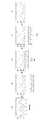
도 1은 본 발명의 일 실시예에 따른 형광막 제조방법을 공정단계에 따라 나타낸 단면도들이다.FIG. 1 is a cross-sectional view illustrating a method of manufacturing a fluorescent film according to an embodiment of the present invention.
도 1(a)를 참조하면, 지지기판(30) 상에 형광막 그린시트(40) 및 유리막 그린시트(50)를 차례로 형성한다.Referring to Fig. 1 (a), a fluorescent film
보다 구체적으로 설명하면, 먼저, 지지기판(30) 상에 형광막 그린시트(40)를 부착할 수 있다.More specifically, first, the
지지기판(30)은 형광막 그린시트(40)를 지지하는 지지기판으로서, 후술하는 소성 단계에서도 견딜 수 있고, 투명한 재질로 이루어진 기판이면 어느 것이나 가능할 것이다. 예를 들어, 지지기판(30)은 유리 기판일 수 있다.The
지지기판(30) 상에 형광막 그린시트(40)를 부착하는 단계는 예컨대, 라미네이션법(lamination)을 이용하여 부착할 수 있다.The step of attaching the
이 때의 형광막 그린시트(40)는 별도의 필름 상에 유리 분말, 형광체 분말 및 유기 바인더를 혼합하여 코팅함으로써 형성될 수 있다. 이 때의 필름은 PET(polyethylene terephthalate) 필름일 수 있다.The fluorescent film
유리 분말은 매트릭스(matrix)가 되는 역할로서, 형광체를 매트릭스 내에 고정시키면서도 투과율을 감소시키지 않는 고투과율 특성을 갖는 물질이면 어느 것이나 가능하다. 예를 들어, 유리 분말은 SiO2-B2O3-RO(R은 Mg, Ca, Sr 또는 Ba)계 유리, SiO2-B2O3계 유리, SiO2-B2O3-R2O(R은 Li, Na 또는 K)계 유리, SiO2-B2O3-Al2O3계 유리, SiO2-B2O3-ZnO계 유리 및 ZnO-B2O3계 유리로 구성된 군에서 선택된 적어도 어느 하나를 포함할 수 있다.The glass powder serves as a matrix, and any material can be used as long as it has a high transmittance characteristic that does not decrease the transmittance while fixing the phosphor in the matrix. For example, the glass powder may be SiO2 -B2 O3 -RO (R is Mg, Ca, Sr or Ba) glass, SiO2 -B2 O3 glass, SiO2 -B2 O3 -R2 O2 -based glass, SiO2 -B2 O3 -Al2 O3 -based glass, SiO2 -B2 O3 -ZnO-based glass, and ZnO-B2 O3 -based glass And at least one selected from the group consisting of < RTI ID = 0.0 >
형광체 분말은 YAG계 형광체, 실리케이트계 형광체, 황화물계 형광체, 질화물계 형광체 또는 이들의 혼합물질을 포함할 수 있다. 예를 들어, 녹색계의 광을 발광하는 형광체 분말은 Ba2SiO4:Eu2+, Sr2SiO4:Eu2+, SrAl2O4:Eu2+, Sr4Al14O25:Eu2+, SrGa2S4:Eu2+, CaGa2S4:Eu2+, SrSi2AlO2-N3:Eu2+, (Ca,Sr,Ba)Si2N2O2:Eu2+, YSiO2N:Tb3+, Y2Si3O3N4:Tb3+, Gd2Si3O3N4:Tb3+ 또는 이들의 혼합물질을 포함할 수 있다. 예를 들어, 적색계의 광을 발광하는 형광체 분말은 Sr3SiO5:Eu2+, SrS:Eu2+, CaS:Eu2+, Sr2Si5N8:Eu2+, Ca2Si5N8:Eu2+, CaAlSiN3, (Ca,Sr,Ba)2Si5N8:Eu2+, LaSi3N5:Eu2+,Sr-α-SiAlON 또는 이들의 혼합물질을 포함할 수 있다.The phosphor powder may include a YAG-base phosphor, a silicate-base phosphor, a sulfide-base phosphor, a nitride-base phosphor, or a mixture thereof. For example, phosphor powder that emits light of green-based lightBa 2 SiO 4: Eu 2 + , Sr 2 SiO 4: Eu 2 +, SrAl 2 O 4: Eu 2 +, Sr 4 Al 14 O 25: Eu 2+, SrGa 2 S 4: Eu 2+, CaGa 2 S 4: Eu 2 +, SrSi 2 AlO 2 -N 3: Eu 2 +, (Ca, Sr, Ba) Si 2 N 2 O 2: Eu 2 +, YSiO2 N: Tb3+ , Y2 Si3 O3 N4 : Tb3+ , Gd2 Si3 O3 N4 : Tb3+, or a mixture thereof. For example, phosphor powder that emits light of the red light isSr 3 SiO 5: Eu 2 + , SrS: Eu 2 +, CaS: Eu 2 +, Sr 2 Si 5 N 8: Eu 2+, Ca 2 Si 5 N8: Eu 2 +, CaAlSiN 3 , (Ca, Sr, Ba) 2 Si 5 N 8: Eu 2 +, LaSi 3 N 5: may includeEu 2 +, Sr-α- SiAlON , or a mixture of these materials .
유기 바인더는 후술하는 소성 공정 중에 번 아웃(burn out)되어, 최종 생성물에는 거의 남지 않는 성분으로 아크릴(Acryl)계 수지(Resin), 비닐(Vinyl)계 수지 또는 실리콘(Silicone)계 수지 등이 사용될 수 있다. 예를 들어, 유기 바인더로 폴리비닐부티랄 수지 또는 메타아크릴 수지를 사용할 수 있다. 한편, 이러한 유기 바인더는 액상 형태로 사용될 수 있다.The organic binder is a component which burns out during the firing process to be described later and hardly remains in the final product, and an acrylic resin, a vinyl resin or a silicone resin is used . For example, a polyvinyl butyral resin or a methacrylic resin may be used as the organic binder. On the other hand, such an organic binder can be used in a liquid form.
한편, 유리 분말, 형광체 분말 및 유기 바인더에 분산제를 더 혼합하여 코팅시켜 그린시트를 제조할 수 있다. 이러한 분산제는 음이온계와 양쪽성 분산제를 주로 사용할 수 있으며 예컨대, 아크릴계 또는 아세테이트계를 사용할 수 있다.On the other hand, a green sheet can be produced by further mixing and coating a glass powder, a phosphor powder and an organic binder with a dispersant. The dispersing agent may be an anionic type and an amphoteric dispersing agent. For example, an acrylic type or an acetate type may be used.
따라서, 이렇게 제조된 형광막 그린시트(40)는 유기 수지 및 무기 고형분을 포함한다. 이러한 유기 수지는 유기 바인더를 포함한다. 또한, 이러한 유기 수지는 분산제를 더 포함할 수 있다. 또한, 이러한 무기 고형분은 매트릭스(matrix)가 되는 유리 성분 및 형광체 성분을 포함한다.Thus, the fluorescent film
유기 수지에 유기 바인더 및 분산제가 포함되고, 무기 고형분에 유리 성분 및 형광체 성분이 포함된 그린시트를 예로 들면, 이러한 그린시트의 조성범위는 질량백분율로, 12% 내지 25%의 유기 수지와 75% 내지 88%의 무기 고형분을 포함할 수 있다.For example, in the case of a green sheet containing an organic binder and a dispersant in an organic resin and containing a glass component and a phosphor component in the inorganic solid content, the composition range of the green sheet is a percentage by mass, an organic resin of 12% to 25% To 88% of inorganic solids.
이 때의 유기 수지의 조성범위는 질량백분율로, 99.2% 내지 99.9%의 유기 바인더 및 0.1% 내지 0.8%의 분산제를 포함할 수 있다.The composition range of the organic resin at this time may include 99.2% to 99.9% of an organic binder and 0.1% to 0.8% of a dispersant in a mass percentage.
이 때의 무기 고형분의 조성범위는 질량백분율로, 60% 내지 90%의 유리 성분 및 10% 내지 40%의 형광체 성분을 포함할 수 있다.In this case, the composition range of the inorganic solid content may include 60% to 90% of the glass component and 10% to 40% of the phosphor component by mass percentage.
그 다음에, 형광막 그린시트(40) 상에 유리막 그린시트(50)를 부착할 수 있다.Then, the glass film
유리막 그린시트(50)는 별도의 필름 상에 유리 분말 및 유기 바인더를 혼합하여 코팅시켜 제조될 수 있다. 한편, 유리 분말 및 유기 바인더를 혼합시에 분산제를 더 혼합하여 코팅시켜 제조될 수 있다. 따라서, 유리막 그린시트(50)의 조성은 유기 수지 및 무기 고형분을 포함할 수 있다. 예컨대, 이러한 유기 수지는 유기 바인더와 분산제를 포함할 수 있고, 이러한 무기 고형분은 유리 성분을 포함할 수 있다.The glass sheet
따라서, 이와 같이 제조된 유리막 그린시트(50)를 형광막 그린시트(40) 상에 부착할 수 있다.Thus, the glass sheet
다만, 경우에 따라 형광막 그린시트(40) 상에 유리막 그린시트(50)를 직접 코팅시켜 제조할 수도 있다.However, the
한편, 형광막 그린시트(40) 상에 유리막 그린시트(50)를 부착하는 단계 이전에, 형광막 그린시트(40)를 소성하여 형광막(41)을 형성하는 단계를 더 포함할 수 있다. 이 경우, 소성된 형광막(41) 상에 유리막 그린시트(50)를 부착할 수 있다. 또한, 형광막(41) 상에 유리막 그린시트(50)를 코팅하여 직접 형성할 수 있다.On the other hand, before the step of attaching the glass sheet
이러한 형광막 그린시트(40) 및 유리막 그린시트(50)는 플렉서블한 특성을 가지고 있기에, 후술하는 몰드 프레싱 공정을 이용하여 다양한 형상을 손쉽게 패터닝할 수 있는 장점이 있다.Since the fluorescent film
도 1(b) 내지 도 1(d)를 참조하면, 상기 형광막 그린시트(40) 및 유리막 그린시트(50)가 형성된 지지기판(30)을 몰드 프레싱하여 유리막 그린시트(50) 상에 패턴을 형성한다.1 (b) to 1 (d), the supporting
예를 들어, 형광막 그린시트(40) 및 유리막 그린시트(50)가 형성된 지지기판(30) 상에 몰드를 사용하여 유리막 그린시트(50)에 압력을 가하여 유리막 그린시트(50) 상에 패턴을 형성할 수 있다.A pressure is applied to the glass film
이 때 사용되는 몰드의 형상은 다양하게 조절할 수 있다. 예를 들어, 몰드 형상 자체를 라운드(round) 형상으로 제작하거나, 쐐기 패턴 형상으로 제작하는 등 다양한 형상으로 제작할 수 있다.The shape of the mold used at this time can be varied. For example, the mold shape itself may be formed into a round shape or a wedge pattern shape.
따라서, 유리막 그린시트(50) 상에 이러한 몰드의 형상에 대응하는 형상으로 패턴이 형성될 수 있다.Therefore, a pattern can be formed on the glass sheet
이러한 유리막 그린시트(50) 상에 형성된 패턴은 홀 패턴, 라인 패턴, 홈 패턴 또는 요철 패턴을 포함할 수 있다. 한편, 이러한 패턴은 마이크로 렌즈 형상의 패턴일 수 있다.The pattern formed on the glass film
도 1(e)를 참조하면, 상기 형광막 그린시트(40) 및 패턴된 유리막 그린시트(50)를 소성하여 형광막(41) 및 패턴된 유리막(51)을 형성한다.Referring to Fig. 1 (e), the fluorescent film
이렇게 형광막 그린시트(40) 및 패턴된 유리막 그린시트(50)를 소성할 경우, 형광막 그린시트(40) 및 유리막 그린시트(50) 내에 포함된 유기 수지는 번 아웃(burn out)되고, 형광막(41) 및 패턴된 유리막(51)이 형성될 수 있다.When the fluorescent film
이 때의 소성 온도는 500℃ 내지 620℃일 수 있다. 만일, 소성 온도가 500℃ 미만인 경우, 그린시트 내의 기포가 제거되지 않아, 투과율이 낮아지는 문제가 있다. 또한, 만일, 소성 온도가 620℃를 상회하는 경우도 그린시트 내에 기포가 생성되어 투과율이 낮아지는 문제가 있다.The firing temperature at this time may be 500 ° C to 620 ° C. If the firing temperature is less than 500 占 폚, bubbles in the green sheet are not removed and the transmittance is lowered. Further, even if the firing temperature exceeds 620 占 폚, bubbles are generated in the green sheet and the transmittance is lowered.
한편, 소성 과정을 통해 유리막 그린시트(50) 상에 형성된 패턴의 형상은 변형될 수도 있다. 예를 들어, 패턴이 각진 형상인 경우, 소성에 의해 라운드지게 변형될 수도 있다. 이렇게 라운드지게 변형될 경우 렌즈 형상이 되므로 광추출 효율이 보다 향상될 수 있다.On the other hand, the shape of the pattern formed on the glass
한편, 지지기판(30) 하부에 렌즈부(60)를 더 형성하는 단계(미도시)를 더 포함할 수 있다. 예를 들어, 지지기판(30)의 아래쪽에 폴리머 비드(Polymer beads) 또는 수지(Resin)를 도포하여 렌즈 형상의 렌즈부를 형성할 수 있다.The method may further include forming a
따라서, 본 발명에 의하면 그린시트를 이용하여 패턴 구조의 형광막을 손쉽게 제조할 수 있고, 나아가 대면적의 플레이트 형광막을 제작할 수 있다.Therefore, according to the present invention, it is possible to easily produce a fluorescent film having a pattern structure by using a green sheet, and further, a plate fluorescent film having a large area can be produced.
이하, 본 발명의 다른 실시예에 따른 형광막 제조방법을 설명한다.Hereinafter, a method of manufacturing a phosphor film according to another embodiment of the present invention will be described.
도 2는 본 발명의 일 실시예에 따른 형광막 제조방법을 공정단계에 따라 나타낸 단면도들이다.FIG. 2 is a cross-sectional view illustrating a method of manufacturing a fluorescent film according to an exemplary embodiment of the present invention. Referring to FIG.
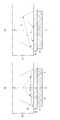
도 2(a)를 참조하면, 지지기판(30) 상에 형광막 그린시트(40) 및 유리막 그린시트(50)를 차례로 형성한다. 이에 대한 형성방법은 도 1(a)에서 상술한 내용과 동일한 바, 자세한 설명은 생략한다.Referring to Fig. 2 (a), a phosphor sheet
도 2(b) 내지 도 2(d)를 참조하면, 상기 형광체막 그린시트(40) 및 유리막 그린시트(50)가 형성된 지지기판(30)을 몰드 프레싱하여 유리막 그린시트(50) 상에 패턴을 형성하되, 상기 형광막 그린시트(40)의 상부에도 패턴이 형성되도록 몰드 프레싱한다.2 (b) to 2 (d), the supporting
이는 형광막 그린시트(40)의 강도와 연신율을 조절함으로써, 유리막 그린시트(50) 뿐만 아니라 형광막 그린시트(40)까지 패턴이 형성될 수 있다. 또한, 몰드 프레싱의 압력을 조절하여, 유리막 그린시트(50)뿐만 아니라 형광막 그린시트(40)까지 패턴을 형성할 수 있다.This can be achieved by adjusting the strength and elongation of the fluorescent film
도 2(e)를 참조하면, 패턴된 형광막 그린시트(40) 및 패턴된 유리막 그린시트(50)를 소성하여 패턴된 형광막(41) 및 패턴된 유리막(51)을 형성한다. 이때의 소성 공정의 내용은 도 1(e)에서 상술한 내용과 동일하다.Referring to FIG. 2 (e), the patterned fluorescent film
한편, 지지기판(30) 하부에 렌즈부(60)를 더 형성하는 단계(미도시)를 더 포함할 수 있다. 예를 들어, 지지기판(30)의 아래쪽에 폴리머 비드(Polymer beads) 또는 수지(Resin)를 도포하여 렌즈 형상의 렌즈부를 형성할 수 있다.The method may further include forming a
본 발명에 의하면, 몰드 프레싱 공정에 의해 패턴된 유리막(51)을 형성할 수 있을 뿐만 아니라, 형광막(41) 상부에도 패턴을 형성할 수 있다. 따라서, 형광막(41) 상부에도 패턴이 형성됨으로써, 형광체 표면적이 증가하여 광 추출 효율이 더욱 향상될 수 있다.According to the present invention, not only the patterned
이하, 본 발명의 다른 실시예에 따른 형광막 제조방법을 설명한다.Hereinafter, a method of manufacturing a phosphor film according to another embodiment of the present invention will be described.
도 3은 본 발명의 일 실시예에 따른 형광막 제조방법을 공정단계에 따라 나타낸 단면도들이다.FIG. 3 is a cross-sectional view illustrating a method of manufacturing a fluorescent film according to an exemplary embodiment of the present invention. Referring to FIG.
도 3(a)를 참조하면, 지지기판(30) 상에 형광막 그린시트(40) 및 유리막 그린시트(50)를 차례로 형성한다. 이는 도 1(a)에서 상술한 내용과 동일하다.3 (a), a phosphor sheet
도 3(b)를 참조하면, 형광막 그린시트(40) 및 유리막 그린시트(50)를 소성하여 형광막(41) 및 유리막(51)을 형성한다. 이 때의 소성온도는 500℃ 내지 620℃일 수 있다.Referring to FIG. 3 (b), the fluorescent film
도 3(c)를 참조하면, 소성된 유리막(51) 상에 패턴을 형성한다.Referring to FIG. 3 (c), a pattern is formed on the fired
소성된 유리막(51) 상에 패턴을 형성하는 단계는 소성된 유리막(51) 상에 레지스트 패턴(미도시)을 형성하는 단계, 레지스트 패턴 사이에 노출된 유리막(51)을 식각하는 단계 및 레지스트 패턴을 제거하는 단계를 포함할 수 있다.The step of forming a pattern on the fired
예를 들어, 유리막(51) 상부에 스핀코팅 등 다양한 방법을 이용하여 레지스트층(미도시)을 형성한 후, 형성된 레지스트층을 패터닝하여 레지스트 패턴을 형성할 수 있다. 그 다음에, 이러한 레지스트층을 리소그라피법을 사용하여 패터닝할 수 있다. 이러한 레지스트 패턴은 홀 패턴 등 다양한 패턴일 수 있다. 그 다음에 레지스트 패턴 사이에 유리막을 화학적 에칭(Chemical Etching) 등의 방법을 이용하여 식각하고, 레지스트 패턴을 제거할 수 있다.For example, a resist layer (not shown) may be formed on the
한편, 도 3(d)를 참조하면, 형광막 그린시트(40) 및 유리막 그린시트(50)를 소성하여 형광막(41) 및 유리막(51)을 형성한 이후에, 소성된 유리막(51) 뿐만 아니라 형광막(41)까지 패턴을 형성할 수 도 있다. 즉, 소성된 형광막(41) 및 유리막(51)에 패턴을 형성하는 단계는 소성된 유리막(51) 상에 레지스트 패턴을 형성하는 단계, 레지스트 패턴 사이에 노출된 유리막(51)을 식각하는 단계, 유리막(51)을 식각하여 노출된 형광막(41)을 식각하는 단계 및 레지스트 패턴을 제거하는 단계를 포함할 수 있다.3 (d), after the fluorescent film
한편, 지지기판(30) 하부에 렌즈부(60)를 더 형성하는 단계(미도시)를 더 포함할 수 있다. 예를 들어, 지지기판(30)의 아래쪽에 폴리머 비드(Polymer beads) 또는 수지(Resin)를 도포하여 렌즈 형상의 렌즈부를 형성할 수 있다.The method may further include forming a
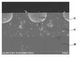
도 4는 본 발명의 일 실시예에 따른 형광막의 SEM 이미지이다.4 is an SEM image of a fluorescent film according to an embodiment of the present invention.
도 4를 참조하면, 유리 지지기판(30) 상에 형성된 형광막 그린시트 및 유리막 그린시트를 550℃에서 소성하여 형광막(41) 및 유리막(51)을 형성한 후, 포토레지스트법 및 화학적 에칭을 통해 유리막(51) 상부에 패턴을 제작하였다. 도시된 바와 같이, 유리막(51)에 홀 패턴이 형성됨을 알 수 있다.4, the fluorescent film green sheet and the glass film green sheet formed on the
또한, 도 5는 본 발명의 일 실시예에 따른 형광막의 SEM 이미지들이다. 도 5(a) 내지 도 5(d)를 참조하면, 패턴의 폭과 간격을 다양하게 조절하여 제조할 수 있음을 알 수 있다. 따라서, 형광체 함량 및 종류에 따라 목적하는 광학적 설계치에 부합하도록 수㎛ 내지 수백㎛의 폭 또는 간격을 갖는 패턴을 제조하여 다양하게 응용할 수 있다.5 is SEM images of a fluorescent film according to an embodiment of the present invention. Referring to FIGS. 5 (a) to 5 (d), it can be seen that the width and spacing of the pattern can be variously adjusted. Accordingly, a pattern having a width or an interval of several micrometers to several hundreds of micrometers can be produced in accordance with a desired optical design value according to the content and type of the phosphor, and various applications can be made.
도 6은 본 발명의 일 실시예에 따른 형광막을 포함하는 발광 소자 패키지를 나타낸 개략도이다.6 is a schematic view illustrating a light emitting device package including a fluorescent film according to an embodiment of the present invention.
도 6을 참조하면, 발광 소자 패키지(1)는 패키지 몸체(10), 발광 소자(20), 지지기판(30), 형광막(41) 및 패턴된 유리막(51)을 포함한다.Referring to FIG. 6, the light emitting
패키지 몸체(10)는 발광 소자(20)가 장착되는 장착부(11)를 구비할 수 있다. 이러한 패키지 몸체(10)에는 장착부(11)에 장착되는 발광 소자(20)와 전기적으로 연결되는 리드(도시되지 않음) 및 히트 싱크(도시되지 않음)가 구비될 수 있으나, 여기에서는 설명을 생략한다.The
도시하는 바와 같이, 장착부(11)는 패키지 몸체(10)의 상면에서 내측으로 함몰된 홈 형상으로 이루어질 수 있고, 따라서, 발광 소자(20)가 장착되는 면 주변에 경사면(12)을 가질 수 있다. 이 경사면(12)은 반사면으로 작용할 수 있다.As shown in the figure, the mounting
또한, 이 장착부(11)는 충진재(도시되지 않음)로 채워질 수 있다. 이러한 충진재는 실리콘 젤이나 에폭시 수지와 같은 물질이 이용될 수 있다. 이러한 충진재는 후술하는 발광 소자(20)를 보호하고 밀봉하는 역할을 한다.Further, the mounting
발광 소자(20)는 장착부(11)에 장착된다. 이러한 발광 소자(20)는 다양한 발광 소자가 이용될 수 있으나, 그 일례로 LED가 이용될 수 있다.The
지지기판(30)은 발광 소자(20)가 장착되는 장착부(11) 상에 위치할 수 있다. 이러한 지지기판(30)은 발광 소자(20)에서 발광되는 광이 외부로 방출하도록 투명 재질의 기판일 수 있다. 따라서, 이러한 지지기판(30)은 도 1 내지 도 3에서 설명한 지지기판(30)을 그대로 이용할 수 있다.The supporting
형광막(41)은 지지기판(30) 상에 위치할 수 있다. 형광막(41)은 발광 소자(20)에서 발광하는 광의 적어도 일부의 파장을 변환할 수 있다. 즉, 형광막(41)은 발광 소자(20)에서 방출하는 광을 흡수하여 변환된 파장의 광을 방출하는 것으로서, 발광 소자 패키지(1)에서는 발광 소자(20) 및 형광막(41)에서 방출하는 광의 혼합된 광이 방출될 수 있다.The
패턴된 유리막(51)은 형광막(41) 상에 위치할 수 있다.The patterned
이러한 형광막 및 패턴된 유리막은 도 1 내지 도 3에서 설명한 바와 같이 형광막 그린시트 및 유리막 그린시트를 이용하여 제조된 것을 특징으로 한다. 예를 들어, 형광막 및 패턴된 유리막은 형광막 그린시트 및 패턴된 유리막 그린시트를 소성하여 제조할 수 있다.The fluorescent film and the patterned glass film are produced using the fluorescent film green sheet and the glass film green sheet as described in Figs. 1 to 3. For example, a fluorescent film and a patterned glass film can be produced by firing a fluorescent film green sheet and a patterned glass film green sheet.
또한, 형광막(41)과 유리막(51)의 구조는 이에 한정되지 않고, 도 1 내지 도 3을 통해 제조될 수 있는 다양한 패턴 구조가 모두 적용될 수 있다. 예컨대, 형광막(41) 및 유리막(51) 둘다 패턴된 구조가 적용될 수 있다.In addition, the structures of the
한편, 지지기판(30)의 하부에 렌즈부(미도시)가 더 위치할 수 있다. 렌즈부는 지지기판(30)의 하부의 적어도 일부에 형성될 수도 있고, 패턴 형상으로 형성될 수도 있다.On the other hand, a lens unit (not shown) may be further disposed under the
도시된 화살표는 발광 소자(20)에서 방출된 광이 패턴된 유리막(51)에서 굴절됨을 나타낸다. 이렇게 굴절된 광이 형광막(41)을 다시 한번 통과함으로써, 형광막(41)의 광변환 효율을 증가시킬 수 있음을 알 수 있다.The arrows shown indicate that the light emitted from the
이하, 지지기판(30)의 하부에 렌즈부가 더 위치하는 경우의 광추출 효율의 향상효과를 설명한다.Hereinafter, the effect of improving the light extraction efficiency in the case where the lens portion is further disposed under the
도 7은 본 발명의 일 실시예에 따른 발광 소자 패키지를 나타낸 개략도들이다.7 is a schematic view illustrating a light emitting device package according to an embodiment of the present invention.
도 7(a) 및 도 7(b)의 발광 소자 패키지는 발광 소자(20)가 장착된 패키지 몸체(10) 상에 지지기판(30) 및 형광막(41)이 위치한다. 다만, 도 7(a)는 지지기판(30)의 하부에 렌즈부가 위치하지 않는 경우이고, 도 7(b)는 지지기판(30)의 하부에 렌즈부(60)가 위치하는 경우이다.7A and 7B, the supporting
도 7(a)를 참조하면, 도시된 화살표는 발광 소자(20)에 의해 발광된 광의 일부가 지지기판(30)의 계면에서 산란되어 패키지 몸체(10) 내에서 소실되는 것을 나타낸다.Referring to FIG. 7 (a), the arrows shown indicate that a part of the light emitted by the
도 7(b)를 참조하면, 도시된 화살표는 발광 소자(20)에 의해 발광된 광이 지지기판(30)의 하부에 위치하는 렌즈부(60)에 의해 외부로 방출되는 것을 나타낸다.Referring to FIG. 7 (b), the arrows indicate that the light emitted by the
즉, 이러한 렌즈부(60)에 의해 도 7(a)와 달리 발광 소자(20)의 광이 패키지 몸체(10)의 내부에서 소실되는 양을 최소화하고, 내부 광의 추출 효율을 향상시킬 수 있음을 알 수 있다.That is, unlike FIG. 7 (a), the
도 8은 본 발명의 일 실시예에 따른 발광 소자 패키지를 나타낸 개략도들이다.8 is a schematic view illustrating a light emitting device package according to an embodiment of the present invention.
도 8(a) 내지 도 8(c)를 참조하면, 발광 소자 패키지는 발광 소자(20)가 장착된 패키지 몸체(10) 상에 지지기판(30) 및 형광막(41)이 위치하고, 지지기판(30)의 하부에 각각 다양한 형상의 렌즈부(60)가 위치하고 있다. 한편, 도 8(c)의 경우, 형광막(41) 상에 패턴된 유리막(51)이 더 위치하고 있다.8A to 8C, in the light emitting device package, the supporting
이러한 다양한 렌즈부(60)의 구조는 광학적 구조 설계 목적에 따라 다양하게 응용될 수 있다.The structure of the
도 9는 본 발명의 일 실시예에 따른 유리막의 패턴 구조의 종횡비에 따른 광추출 효율을 설명하기 위한 발광 소자 패키지의 개략도이다.9 is a schematic view of a light emitting device package for explaining light extraction efficiency according to an aspect ratio of a pattern structure of a glass film according to an embodiment of the present invention.
도 9를 참조하면, 발광 소자 패키지는 발광 소자(20)가 장착된 패키지 몸체(10) 상에 지지기판(30) 및 패턴된 형광막(41)이 위치한다.Referring to FIG. 9, the light emitting device package includes a supporting
이 때, 형광막(41)의 패턴 구조의 종횡비(Aspect Ratio)를 높여서 반사형 형광막(41)이 형성된다. 이 때의 형광막(41)의 패턴의 종횡비는 2 대 1 이상 일 수 있다. 만일, 형광막(41)의 패턴의 종횡비가 2 대 1보다 작은 경우 패턴 구조에 의한 반사효과가 충분하지 않을 수 있다. 바람직하게, 이 때의 형광막(41)의 패턴의 종횡비는 2 대 1 내지 6 대 1일 수 있다.At this time, the aspect ratio of the pattern structure of the
한편, 경우에 따라, 패턴된 형광막(41) 상에 형광막(41)의 패턴에 대응하여 패턴된 유리막(미도시)이 더 위치할 수 있다. 이 경우, 형광막과 유리막에 형성된 패턴 전체를 고려하여 종횡비를 조절할 수 있다.On the other hand, a glass film (not shown) patterned corresponding to the pattern of the
따라서, 형광막(41)의 패턴의 종횡비를 2 대 1 내지 6 대 1로 제작함으로써, 패턴 구조가 없는 형광막(투과형 형광막)보다 높은 효율을 갖는 반사형 형광막을 제작할 수 있다.Therefore, by fabricating the aspect ratio of the pattern of the
이하, 반사형 형광막의 외부로 광추출되는 효율의 증가를 광학 시뮬레이션 결과를 통하여 설명한다.Hereinafter, an increase in the efficiency of light extraction to the outside of the reflection type fluorescent film will be described through the results of optical simulation.
도 10은 본 발명의 일 실시예에 따른 형광막(41)의 광학 시뮬레이션 결과를 나타낸 도면들이다.10 is a diagram showing the results of optical simulation of the
도 10(a)를 참조하면, 발광 소자 패키지는 발광 소자(20)가 장착된 패키지 몸체(10) 상에 패턴되지 않은 형광막(41)을 포함한 경우이고, 도 10(b)를 참조하면, 발광 소자 패키지는 발광 소자(2)가 장착된 패키지 몸체(10) 상에 지지기판(30) 및 패턴된 형광막(41)을 포함한 경우이다. 이 때의 발광 소자(20)는 청색광을 발광하는 발광 다이오드이다.10A, a light emitting device package includes a patterned
도 10(a)의 발광 소자 패키지에서, 발광 소자(20)에서 발광된 광이 일부는 내부로 산란되어 소실되고 일부는 형광막(41)을 투과하여 외부로 방출된다.In the light emitting device package of Fig. 10 (a), the light emitted from the
보다 구체적으로 설명하면, 발광 소자(20)에서 발출된 청색광의 형광막 투과율은 30%, 패키지 내부로의 back 반사율은 20%, 형광막 흡수율은 50%이다. 이 때, 형광막(41)에 흡수된 흡수광의 가시광 변환효율은 70%인 바, 형광막 흡수율인 50%에 가시광 변환효율인 70%를 곱한 값인 35%가 변환된 가시광이다. 또한, 변환된 가시광의 패키지 내부로의 back 반사율은 40%이므로 최종적으로 외부로 투과되는 가시광은 21%이다. 따라서, 청색광으로 형광막(41)을 투과한 30%와 청색광이 형광막(41)에서 가시광으로 변환되어 외부로 방출된 21%를 더하면 최종 투과된 광은 51%가 된다.More specifically, the transmittance of the blue light emitted from the
도 10(b)의 발광 소자 패키지에서도 발광 소자(20)에서 발광된 광이 일부는 내부로 산란되어 소실되고 일부는 형광막(41)을 투과하여 외부로 방출된다.In the light emitting device package of FIG. 10 (b), part of the light emitted from the
보다 구체적으로 설명하면, 발광 소자(20)에서 방출된 청색광의 형광막 투과율은 30%, 패키지 내부로의 back 반사율은 30%, 형광막 흡수율은 40%이다. 이 때, 형광막(41)에 흡수된 흡수광의 가시광 변환효율은 70%인 바, 형광막 흡수율인 40%에 가시광 변환효율인 70%를 곱한 값인 28%가 변환된 가시광이다. 또한, 변환된 가시광의 패키지 내부로의 back 반사율은 10%이므로 최종적으로 외부로 투과되는 가시광은 약 25%이다. 따라서, 청색광으로 형광막(41)을 투과한 30%와 청색광이 형광막(41)에서 가시광으로 변환되어 외부로 방출된 25%를 더하면 최종 투과된 광은 55%가 된다.More specifically, the transmittance of the blue light emitted from the
도 10(b)의 반사형 형광막은 패턴을 형성하기 위해 형광막의 일부가 식각되어 형광막 흡수율이 감소된다. 즉, 형광막의 광 흡수율은 40%로서, 도 10(a)의 투과형 형광막의 광 흡수율인 50%보다 작게 된다.In the reflection type fluorescent film of Fig. 10 (b), a part of the fluorescent film is etched to form a pattern, so that the absorption rate of the fluorescent film is reduced. That is, the light absorption rate of the fluorescent film is 40%, which is smaller than the light absorption rate of 50% of the transmission type fluorescent film of Fig. 10 (a).
다만, 반사형 형광막에 흡수된 광이 반사형 형광막의 패턴 구조에 의해 반사되어 외부로 나가는 비중이 증가된다. 따라서, 반사형 형광막의 변환된 가시광의 back 반사율은 투과형 형광막의 변환된 가시광의 back 반사율인 40%보다 매우 작은 10%가 된다.However, the light absorbed by the reflection type fluorescent film is reflected by the pattern structure of the reflection type fluorescent film and the specific gravity going out is increased. Therefore, the back reflectance of the converted visible light of the reflective fluorescent film becomes 10%, which is much smaller than the back reflectance of 40% of the converted visible light of the transmissive fluorescent film.
따라서, 최종적으로 외부로 투과된 광은 반사형 형광막을 이용한 경우가 투과형 형광막을 이용한 경우보다 10% 가까이 효율이 증가함을 알 수 있다.Therefore, it can be seen that the efficiency of the ultraviolet light which is finally transmitted to the outside is increased by about 10% when the reflective fluorescent film is used, compared to the case using the transmissive fluorescent film.
따라서, 본 발명에 의하면, 형광막 그린시트 및 유리막 그린시트를 이용하여 형광막 또는 형광막 및 유리막에 패턴을 형성하고, 이러한 패턴의 종횡비를 높여 반사형 형광막을 제조함으로써, 외부로 방출되는 광추출 효율을 보다 향상시킬 수 있다.Therefore, according to the present invention, a pattern is formed on a fluorescent film or a fluorescent film and a glass film by using a fluorescent film green sheet and a glass film green sheet, and the reflection type fluorescent film is produced by increasing the aspect ratio of such pattern, The efficiency can be further improved.
이하, 본 발명의 일 실시예에 따른 조명장치에 대하여 도 11 및 도 12를 참조하여 설명한다.Hereinafter, a lighting apparatus according to an embodiment of the present invention will be described with reference to Figs. 11 and 12. Fig.
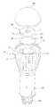
도 11은 본 발명의 일 실시예에 따른 조명장치의 사시도이고, 도 12는 본 발명의 일 실시예에 따른 조명장치의 분리 사시도이다.FIG. 11 is a perspective view of a lighting apparatus according to an embodiment of the present invention, and FIG. 12 is an exploded perspective view of a lighting apparatus according to an embodiment of the present invention.
도 11 및 도 12를 참조하면, 조명장치는 히트싱크(100), 렌즈 유닛(200), 발광 유닛(300), 전장부(미도시), 케이스(500) 및 전원 소켓(600)을 포함한다.11 and 12, the lighting apparatus includes a
히트싱크(Heat sink, H, 100)는 외관을 형성하며 중공부(111)를 갖는 외측 하우징(110) 및 이러한 중공부(111)에 배치되며, 길이방향으로 연장된 내측 하우징(120)을 포함할 수 있다.A
외측 하우징(110)은 조명장치가 작동 시, 발광 유닛(300)에서 발생하는 열을 외부로 발산하기 위하여 무게가 가볍고 열 전도성이 높은 재질로 형성될 수 있고, 바람직하게 수지 재질로 형성될 수 있다.The
중공부(111)는 외측 하우징(110)의 길이방향을 따라 관통하여 형성되어 있고, 예컨대, 중공부(111)는 실린더 형상을 가질 수 있다. 이러한 중공부(111)에는 내측 하우징(120), 전장부, 케이스(500) 등이 삽입될 수 있다.The
내측 하우징(120)은 외측 하우징(110)의 중공부(111)에 마련된다. 내측 하우징(120)에는 외측 하우징(110)을 향하여 돌출된 복수의 핀을 마련할 수 있다. 이러한 핀들은 내측 하우징(120)의 표면적을 증가시키고, 내측 하우징(120)과 외측 하우징(110)의 접촉 면적을 증가시켜 방열 효율을 향상킬 수 있다.The
따라서, 발광 유닛(300)에서 발생한 열은 내측 하우징(120)으로 전달되고, 내측 하우징(120)으로 전달된 열은 외측 하우징(110)을 통해 외부로 발산되며, 조명장치의 방열이 이루어진다.The heat generated in the
렌즈 유닛(200)은 외측 하우징(110)에 장착된다. 렌즈 유닛(200)은 외측 하우징(110)에 장착된 발광 유닛(300)에서 방출되는 빛을 외부로 안내하는 기능을 수행하고, 적어도 하나 이상의 집광렌즈를 포함할 수 있다.The
이러한 렌즈 유닛(200)은 발광 유닛(300)에서 방출되는 빛을 확산시켜 발광 효율을 향상시킬 수 있도록, 폴리카보네이트 또는 아크릴 등의 수지로 이루어진 확산판을 벌브(bulb) 형태로 성형하는 것으로 제조될 수 있다.The
발광 유닛(300)은 기판(310)과 기판(310)에 실장된 발광 소자 패키지(1)를 포함한다. 이러한 기판(310)은 인쇄회로기판일 수 있다. 예를 들어, 발광 소자 패키지(1)는 인쇄회로기판 상에 표면실장기술(SMT) 방식으로 부착될 수 있다.The
이러한 발광 소자 패키지(1)는 도 1 내지 도 3에서 설명한 제조방법에 의해 제조된 형광막을 포함할 수 있다. 또한, 이러한 발광 소자 패키지(1)는 도 6 내지 도 10에서 설명한 발광 소자 패키지(1)일 수 있다. 따라서, 이에 대한 자세한 설명은 생략한다.The light emitting
한편, 발광 유닛(300)은 내측 하우징(120)에 장착될 수 있다. 즉, 발광 유닛(300)의 기판(310)은 내측 하우징(120)에 체결될 수 있다. 이를 위하여 조명 장치는 발광 유닛(300)의 기판(310)을 관통하여 내측 하우징(120)에 고정되는 체결수단(미도시)을 추가로 포함할 수 있다.Meanwhile, the
이러한 체결수단은 스크류일 수 있으며, 기판(310)에는 발광 다이오드 발광 다이오드 패키지(10)가 실장된 일면과 그 배면을 관통하는 제1 체결홀(311)이 마련되고, 내측 하우징(120)에는 제1 체결홀(311)과 대응되는 위치에 제2 체결홀(121)이 마련될 수 있다.The fastening means may be a screw and a
한편, 조명 장치는 발광 유닛(300)과 내측 하우징(120) 사이에 배치되는 열전도 패드(400)를 추가로 포함할 수 있다. 이러한 열전도 패드(400)가 발광 유닛(300)과 내측 하우징(120) 사이에 배치되는 경우 열전도 패드(400)에는 기판(310)의 제1 체결홀(311) 및 내측 하우징(120)의 제2 체결홀(121)과 대응되는 위치에 제3 체결홀(401)이 마련될 수 있다. 따라서, 이러한 구조에서 상술한 체결수단에 의하여 발광 유닛(300)과 열전도 패드(400)가 내측 하우징(120)에 고정될 수 있다.Meanwhile, the lighting device may further include a heat
따라서, 열전도 패드(400)는 발광 유닛(300)과 내측 하우징(120) 사이의 열 전달 성능을 높이고, 발광 유닛(300)과 내측 하우징(120)의 접촉면적을 증가시켜 방열 효율을 향상시킬 수 있다.The
전장부(미도시)는 외측 하우징(110)의 중공부(111)에 배치되며, 발광 유닛(300)과 전기적으로 연결된다. 이러한 전장부는 발광 유닛(300)에 전원을 공급하며, 발광 유닛과 전기적으로 연결되는 회로부 및 이러한 회로부를 절연시키기 위하여 회로부와 케이스 사이 공간에 충진되는 절연부를 포함할 수 있다.(Not shown) is disposed in the
한편, 회로부와 케이스 사이 공간에 충진되는 절연부는 실리콘으로 형성될 수 있다.Meanwhile, the insulating portion filled in the space between the circuit portion and the case may be formed of silicon.
케이스(500)는 전장부를 둘러싸며 외측 하우징(110)의 중공부(111)에 삽입된다. 예를 들어, 케이스(500)는 일부 영역이 내측 하우징(120) 내부에 배치되도록 외측 하우징(110)의 중공부(111)에 삽입될 수 있다.The
또한, 케이스(500) 및 외측 하우징(110)의 중공부(111)에는 케이스(500)의 용이한 삽입을 위한 구조가 각각 마련될 수 있다. 일 예로서, 케이스(500)의 외주면에는 가이드 돌기(미도시)가 마련될 수 있고, 외측 하우징(110)의 중공부(111)의 내주면에는 삽입과정에서 케이스(500)의 가이드 돌기가 안내되는 가이드 홈부(미도시)가 마련될 수 있다.In addition, the
전원 소켓(600)은 케이스(500)에 장착될 수 있다.The
한편, 본 명세서와 도면에 개시된 본 발명의 실시 예들은 이해를 돕기 위해 특정 예를 제시한 것에 지나지 않으며, 본 발명의 범위를 한정하고자 하는 것은 아니다. 여기에 개시된 실시 예들 이외에도 본 발명의 기술적 사상에 바탕을 둔 다른 변형 예들이 실시 가능하다는 것은, 본 발명이 속하는 기술 분야에서 통상의 지식을 가진 자에게 자명한 것이다.It should be noted that the embodiments of the present invention disclosed in the present specification and drawings are only illustrative of specific examples for the purpose of understanding and are not intended to limit the scope of the present invention. It will be apparent to those skilled in the art that other modifications based on the technical idea of the present invention are possible in addition to the embodiments disclosed herein.
1: 발광 소자 패키지10: 패키지 몸체
20: 발광 소자30: 지지기판
40: 형광막 그린시트41: 형광막
50: 유리막 그린시트51: 유리막
60: 렌즈부100: 히트싱크
110: 외측 하우징111: 중공부
120: 내측 하우징200: 렌즈 유닛
300: 발광 유닛310: 기판
400: 열전도 패드500: 케이스
600: 전원 소켓1: Light emitting device package 10: Package body
20: light emitting element 30: support substrate
40: fluorescent film green sheet 41: fluorescent film
50: glass sheet green sheet 51: glass sheet
60: Lens part 100: Heat sink
110: outer housing 111: hollow
120: inner housing 200: lens unit
300: light emitting unit 310: substrate
400: heat conduction pad 500: case
600: Power socket
Claims (15)
Translated fromKorean상기 형광막 그린시트 상에 유리막 그린시트를 부착하는 단계;
상기 형광막 그린시트 및 유리막 그린시트가 형성된 지지기판을 몰드 프레싱하여 상기 유리막 그린시트 상에 패턴을 형성하는 단계; 및
상기 형광막 그린시트 및 패턴된 유리막 그린시트를 소성하여 형광막 및 패턴된 유리막을 형성하는 단계를 포함하는 형광막 제조방법.Attaching a green sheet of fluorescent film on a support substrate;
Attaching a glass film green sheet on the fluorescent film green sheet;
Forming a pattern on the glass film green sheet by mold pressing the support substrate on which the fluorescent film green sheet and the glass film green sheet are formed; And
And firing the fluorescent film green sheet and the patterned glass film green sheet to form a fluorescent film and a patterned glass film.
상기 몰드 프레싱하여 상기 유리막 그린시트 상에 패턴을 형성하는 단계는 상기 형광막 그린시트의 상부에도 패턴이 형성되도록 몰드 프레싱하는 것을 특징으로 하는 형광막 제조방법.The method according to claim 1,
Wherein the step of forming a pattern on the green sheet green sheet by the mold pressing comprises a step of molding pressing the green sheet to form a pattern on the green sheet.
상기 유리막 그린시트를 부착하는 단계 이전에,
상기 형광막 그린시트를 소성하여 형광막을 형성하는 단계를 더 포함하는 형광막 제조방법.The method according to claim 1,
Prior to attaching the glass sheet green sheet,
And firing the fluorescent film green sheet to form a fluorescent film.
상기 형광막 그린시트 상에 유리막 그린시트를 부착하는 단계;
상기 형광막 그린시트 및 유리막 그린시트를 소성하여 형광막 및 유리막을 형성하는 단계; 및
상기 소성된 유리막 상에 패턴을 형성하는 단계를 포함하는 형광막 제조방법.Attaching a green sheet of fluorescent film on a support substrate;
Attaching a glass film green sheet on the fluorescent film green sheet;
Baking the fluorescent film green sheet and the glass film green sheet to form a fluorescent film and a glass film; And
And forming a pattern on the fired glass film.
상기 형광막 그린시트는 필름 상에 유리 분말, 형광체 분말, 유기 바인더 및 분산제를 혼합하여 코팅시켜 형성된 것을 특징으로 하는 형광막 제조방법.The method according to claim 1 or 4,
Wherein the fluorescent film green sheet is formed by mixing a glass powder, a phosphor powder, an organic binder and a dispersing agent on a film to form a coating.
상기 소성 온도는 500℃ 내지 620℃인 것을 특징으로 하는 형광막 제조방법.The method according to claim 1 or 4,
Wherein the baking temperature is 500 ° C to 620 ° C.
상기 지지기판 하부에 렌즈부를 형성하는 단계를 더 포함하는 형광막 제조방법.5. The method according to any one of claims 1 to 4,
And forming a lens portion below the support substrate.
상기 패턴을 형성하는 단계는,
상기 소성된 유리막 및 형광막에 패턴을 형성하는 것을 특징으로 하는 형광막 제조방법.5. The method of claim 4,
Wherein forming the pattern comprises:
And forming a pattern on the fired glass film and the fluorescent film.
상기 패턴은 홀 패턴, 라인 패턴, 홈 패턴 또는 요철 패턴을 포함하는 형광막 제조방법.5. The method according to any one of claims 1 to 4,
Wherein the pattern comprises a hole pattern, a line pattern, a groove pattern, or a concavo-convex pattern.
상기 유리막 및 형광막의 패턴의 종횡비(aspect ratio)는 2 대 1 내지 6 대 1인 것을 특징으로 하는 형광막 제조방법.9. The method of claim 8,
Wherein the aspect ratio of the patterns of the glass film and the fluorescent film is 2: 1 to 6: 1.
상기 장착부에 장착되는 발광 소자;
상기 발광 소자 상에 위치하는 지지기판;
상기 지지기판 상에 위치하는 형광막; 및
상기 형광막 상에 위치하는 패턴된 유리막을 포함하는 발광 소자 패키지.A package body having a mounting portion;
A light emitting element mounted on the mounting portion;
A supporting substrate positioned on the light emitting element;
A fluorescent film disposed on the supporting substrate; And
And a patterned glass film disposed on the fluorescent film.
상기 형광막의 상부는 패턴된 것을 특징으로 하는 발광 소자 패키지.13. The method of claim 12,
Wherein an upper portion of the fluorescent film is patterned.
상기 지지기판의 하부에 형성된 렌즈부를 더 포함하는 발광 소자 패키지.The method according to claim 12 or 13,
And a lens portion formed at a lower portion of the supporting substrate.
상기 형광막 및 패턴된 유리막은 형광막 그린시트 및 패턴된 유리막 그린시트를 소성하여 제조된 것을 특징으로 하는 발광 소자 패키지.13. The method of claim 12,
Wherein the fluorescent film and the patterned glass film are manufactured by firing a fluorescent film green sheet and a patterned glass film green sheet.
Priority Applications (3)
| Application Number | Priority Date | Filing Date | Title |
|---|---|---|---|
| KR1020120146185AKR20140077408A (en) | 2012-12-14 | 2012-12-14 | Method for manufacturing phosphor film and the phosphor film manufactured by the same |
| EP13176341.9AEP2743999B1 (en) | 2012-12-14 | 2013-07-12 | Light emitting device package including phosphor film, and method of manufacturing the same. |
| US13/951,277US20140167605A1 (en) | 2012-12-14 | 2013-07-25 | Light emitting device package including phosphor film, method of manufacturing the same, and lighting apparatus using the same |
Applications Claiming Priority (1)
| Application Number | Priority Date | Filing Date | Title |
|---|---|---|---|
| KR1020120146185AKR20140077408A (en) | 2012-12-14 | 2012-12-14 | Method for manufacturing phosphor film and the phosphor film manufactured by the same |
Publications (1)
| Publication Number | Publication Date |
|---|---|
| KR20140077408Atrue KR20140077408A (en) | 2014-06-24 |
Family
ID=48771354
Family Applications (1)
| Application Number | Title | Priority Date | Filing Date |
|---|---|---|---|
| KR1020120146185ACeasedKR20140077408A (en) | 2012-12-14 | 2012-12-14 | Method for manufacturing phosphor film and the phosphor film manufactured by the same |
Country Status (3)
| Country | Link |
|---|---|
| US (1) | US20140167605A1 (en) |
| EP (1) | EP2743999B1 (en) |
| KR (1) | KR20140077408A (en) |
Families Citing this family (8)
| Publication number | Priority date | Publication date | Assignee | Title |
|---|---|---|---|---|
| CN106030836B (en)* | 2014-03-10 | 2019-04-05 | 欧司朗光电半导体有限公司 | Wavelength conversion element, light-emitting semiconductor component, and manufacturing method thereof |
| CN104175578A (en)* | 2014-07-08 | 2014-12-03 | 华南师范大学 | Manufacturing method of LED fluorescent powder prefabricated film |
| WO2016087600A1 (en)* | 2014-12-04 | 2016-06-09 | Osram Sylvania Inc. | Method for producing a ceramic conversion element, ceramic conversion element and optoelectronic device |
| KR102252992B1 (en) | 2014-12-12 | 2021-05-20 | 삼성전자주식회사 | Method for manufacturing semiconductor light emitting device package |
| JP6602111B2 (en)* | 2015-08-28 | 2019-11-06 | 三星電子株式会社 | Semiconductor light emitting device |
| DE102016105988A1 (en)* | 2016-04-01 | 2017-10-05 | Osram Opto Semiconductors Gmbh | Converter for partial conversion of a primary radiation and light-emitting component |
| JP7187879B2 (en)* | 2018-08-08 | 2022-12-13 | セイコーエプソン株式会社 | Wavelength conversion element, light source device and projector |
| CN112563397A (en)* | 2020-12-07 | 2021-03-26 | 扬州中科半导体照明有限公司 | LED chip array module and manufacturing method thereof |
Family Cites Families (10)
| Publication number | Priority date | Publication date | Assignee | Title |
|---|---|---|---|---|
| US6023130A (en)* | 1995-09-06 | 2000-02-08 | Kyocera Corporation | Plasma display substrate and a production method thereof |
| JP2002267956A (en)* | 2001-03-08 | 2002-09-18 | Sony Corp | Micromirror and method of manufacturing the same |
| US20050046321A1 (en)* | 2001-10-31 | 2005-03-03 | Yoshinori Suga | Display apparatus |
| CN100511732C (en)* | 2003-06-18 | 2009-07-08 | 丰田合成株式会社 | Light emitting device |
| US8481977B2 (en)* | 2006-03-24 | 2013-07-09 | Goldeneye, Inc. | LED light source with thermally conductive luminescent matrix |
| JP4978886B2 (en)* | 2006-06-14 | 2012-07-18 | 日本電気硝子株式会社 | Phosphor composite material and phosphor composite member |
| WO2009119034A1 (en)* | 2008-03-26 | 2009-10-01 | Panasonic Corporation | Semiconductor light-emitting apparatus |
| CN102782089B (en)* | 2010-02-04 | 2015-07-22 | 日东电工株式会社 | Luminescent ceramic laminate and manufacturing method thereof |
| JP2012182376A (en)* | 2011-03-02 | 2012-09-20 | Stanley Electric Co Ltd | Wavelength conversion member and light source device |
| US9115868B2 (en)* | 2011-10-13 | 2015-08-25 | Intematix Corporation | Wavelength conversion component with improved protective characteristics for remote wavelength conversion |
- 2012
- 2012-12-14KRKR1020120146185Apatent/KR20140077408A/ennot_activeCeased
- 2013
- 2013-07-12EPEP13176341.9Apatent/EP2743999B1/enactiveActive
- 2013-07-25USUS13/951,277patent/US20140167605A1/ennot_activeAbandoned
Also Published As
| Publication number | Publication date |
|---|---|
| EP2743999B1 (en) | 2019-09-04 |
| US20140167605A1 (en) | 2014-06-19 |
| EP2743999A3 (en) | 2016-11-09 |
| EP2743999A2 (en) | 2014-06-18 |
Similar Documents
| Publication | Publication Date | Title |
|---|---|---|
| KR20140077408A (en) | Method for manufacturing phosphor film and the phosphor film manufactured by the same | |
| CN101711435B (en) | Lighting device with wavelength converting element held by support structure with opening | |
| JP6646593B2 (en) | LED lighting unit | |
| JP5318976B2 (en) | Lamp cover and LED lamp using the same | |
| CN104205378B (en) | LED modules with highly reflective carrier | |
| TWI614452B (en) | Photoluminescence wavelength conversion member for solid state light emitting device and lamp | |
| US9897789B2 (en) | Light emitting device package and lighting device having the same | |
| CN102563405B (en) | Comprise the means of illumination of photoluminescent sheet | |
| US20100181582A1 (en) | Light emitting devices with phosphor wavelength conversion and methods of manufacture thereof | |
| CN101365907B (en) | Illumination system and display device | |
| US20120153311A1 (en) | Low-cost solid-state based light emitting devices with photoluminescent wavelength conversion and their method of manufacture | |
| CN108987551A (en) | The manufacturing method of light emitting device and light emitting device | |
| CN105588008A (en) | Light source module and lighting device having the same | |
| CN103547858A (en) | LED-Based Light Sources for Light-Emitting Devices and Lighting Arrangements with Photoluminescence Wavelength Conversion | |
| CN102165613A (en) | LEDs with controlled angular non-uniformity | |
| CN102859259A (en) | LED based pedestal-type lighting structure | |
| CN105190916A (en) | Light emitting device with wavelength conversion layer | |
| TW201220549A (en) | Light source, device including light source, and/or methods of making the same | |
| CN103190007A (en) | Optic assembly utilizing quantum dots | |
| KR20160079973A (en) | Light source module | |
| JP2016076699A (en) | Light emitting device | |
| KR20130016940A (en) | Lighting device | |
| JP2012009696A (en) | Light emitting device and led illuminating equipment | |
| TW201403870A (en) | Light emitting diode element and manufacturing mathod thereof | |
| KR101701746B1 (en) | Led lighting device |
Legal Events
| Date | Code | Title | Description |
|---|---|---|---|
| PA0109 | Patent application | Patent event code:PA01091R01D Comment text:Patent Application Patent event date:20121214 | |
| PG1501 | Laying open of application | ||
| A201 | Request for examination | ||
| PA0201 | Request for examination | Patent event code:PA02012R01D Patent event date:20171018 Comment text:Request for Examination of Application Patent event code:PA02011R01I Patent event date:20121214 Comment text:Patent Application | |
| E902 | Notification of reason for refusal | ||
| PE0902 | Notice of grounds for rejection | Comment text:Notification of reason for refusal Patent event date:20180821 Patent event code:PE09021S01D | |
| E601 | Decision to refuse application | ||
| PE0601 | Decision on rejection of patent | Patent event date:20190208 Comment text:Decision to Refuse Application Patent event code:PE06012S01D Patent event date:20180821 Comment text:Notification of reason for refusal Patent event code:PE06011S01I |