KR20140070340A - Oled display device having touch sensor and method of fabricating the same - Google Patents
Oled display device having touch sensor and method of fabricating the sameDownload PDFInfo
- Publication number
- KR20140070340A KR20140070340AKR1020130091068AKR20130091068AKR20140070340AKR 20140070340 AKR20140070340 AKR 20140070340AKR 1020130091068 AKR1020130091068 AKR 1020130091068AKR 20130091068 AKR20130091068 AKR 20130091068AKR 20140070340 AKR20140070340 AKR 20140070340A
- Authority
- KR
- South Korea
- Prior art keywords
- routing
- base layer
- layer
- touch electrodes
- routing wiring
- Prior art date
- Legal status (The legal status is an assumption and is not a legal conclusion. Google has not performed a legal analysis and makes no representation as to the accuracy of the status listed.)
- Granted
Links
Images


Classifications
- G—PHYSICS
- G06—COMPUTING OR CALCULATING; COUNTING
- G06F—ELECTRIC DIGITAL DATA PROCESSING
- G06F3/00—Input arrangements for transferring data to be processed into a form capable of being handled by the computer; Output arrangements for transferring data from processing unit to output unit, e.g. interface arrangements
- G06F3/01—Input arrangements or combined input and output arrangements for interaction between user and computer
- G06F3/03—Arrangements for converting the position or the displacement of a member into a coded form
- G06F3/041—Digitisers, e.g. for touch screens or touch pads, characterised by the transducing means
- G06F3/0412—Digitisers structurally integrated in a display
- H—ELECTRICITY
- H10—SEMICONDUCTOR DEVICES; ELECTRIC SOLID-STATE DEVICES NOT OTHERWISE PROVIDED FOR
- H10K—ORGANIC ELECTRIC SOLID-STATE DEVICES
- H10K59/00—Integrated devices, or assemblies of multiple devices, comprising at least one organic light-emitting element covered by group H10K50/00
- H10K59/40—OLEDs integrated with touch screens
- G—PHYSICS
- G06—COMPUTING OR CALCULATING; COUNTING
- G06F—ELECTRIC DIGITAL DATA PROCESSING
- G06F2203/00—Indexing scheme relating to G06F3/00 - G06F3/048
- G06F2203/041—Indexing scheme relating to G06F3/041 - G06F3/045
- G06F2203/04103—Manufacturing, i.e. details related to manufacturing processes specially suited for touch sensitive devices
Landscapes
- Engineering & Computer Science (AREA)
- General Engineering & Computer Science (AREA)
- Theoretical Computer Science (AREA)
- Human Computer Interaction (AREA)
- Physics & Mathematics (AREA)
- General Physics & Mathematics (AREA)
- Electroluminescent Light Sources (AREA)
Abstract
Translated fromKoreanDescription
Translated fromKorean본 발명은 터치 센서를 구비하는 표시장치 및 그 제조방법에 관한 것으로, 특히 두께와 무게를 줄이고 제조비용을 줄일 수 있는 터치 센서를 구비하는 유기 발광 다이오드(Organic Light Emitting Diodes, OLED)표시장치 및 그 제조방법에 관한 것이다.
The present invention relates to a display device having a touch sensor and a manufacturing method thereof, and more particularly to an organic light emitting diode (OLED) display device having a touch sensor capable of reducing thickness and weight and manufacturing cost, And a manufacturing method thereof.
최근, 평판 디스플레이 시장은 액정표시장치(Liquid Crystal Display, LCD)와 OLED 표시장치가 주류를 이루고 있다. 이 중 OLED 표시장치는 LCD와 다르게 자발광소자로서, LCD에 사용되는 백라이트가 필요하지 않고, 경량 박형이 가능해 점차 시장을 넓혀가고 있다.2. Description of the Related Art In recent years, the flat panel display market is mainly comprised of a liquid crystal display (LCD) and an OLED display. Of these, OLED display devices are self-luminous devices unlike LCDs, and do not require a backlight used in LCDs. Lightweight thin type OLED display devices are gradually expanding the market.
또한, 최근에는 플렉서블(flexible) 플라스틱이나 메탈 호일(metal foil)과 같이 유연성 있는 재료를 기판으로 사용하여 종이처럼 휘어져도 표시성능을 그대로 유지할 수 있게 제조된 플렉서블(flexible) OLED 표시장치가 차세대 평판표시장치로 급부상중이다.In recent years, flexible OLED display devices, which are manufactured using a flexible material such as a flexible plastic or a metal foil as a substrate and capable of maintaining the display performance even when bent like paper, It is emerging as a device.
이 플렉서블 OLED 표시장치의 기판은 경량이고, 내충격성이 우수하며 저렴한 장점을 갖는 반면, 외부로부터 수분 또는 산소의 침투가 용이한 단점이 있다.The substrate of this flexible OLED display device is lightweight, has excellent impact resistance and is inexpensive, but has a disadvantage that moisture or oxygen can easily penetrate from the outside.
이와 같은 이유로, 플렉서블 OLED 표시장치는 적어도 3층으로 이뤄진 보호필름(13)을 포함해 구성된다.For this reason, the flexible OLED display device is composed of a protective film 13 consisting of at least three layers.
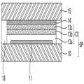
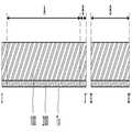
이하, 도 1a 및 도 1b를 참조하여, 종래의 플렉서블 OLED 표시장치에 대해 상세히 설명하기로 한다. 도 1a는 종래의 플렉서블 OLED 표시장치을 개략적으로 도시한 단면도이고 도 1b는 종래의 터치센서를 구비하는 OLED표시장치에 관한 것으로, 도 1a의 OLED 표시장치에 적용된 터치 센서를 도시한 단면도이다.Hereinafter, a conventional flexible OLED display device will be described in detail with reference to FIGS. 1A and 1B. FIG. 1A is a cross-sectional view schematically illustrating a conventional flexible OLED display, FIG. 1B is a cross-sectional view illustrating a touch sensor applied to the OLED display of FIG. 1A, and FIG.
도 1a를 참조하면, 플렉서블 OLED 표시장치는 데이터 라인들, 게이트 라인들 및 박막 트랜지스터 등의 표시소자가 형성된 박막 트랜지스터(TFT) 기판(10)과, TFT 기판(10) 상에 형성되는 유기 발광다이오드(OLED)(11)와, TFT 기판(10)과 OLED(11)를 인캡슐레이트하는 보호막(13)을 포함한다.1A, a flexible OLED display device includes a thin film transistor (TFT) substrate 10 on which display elements such as data lines, gate lines, and thin film transistors are formed, and an organic light emitting diode (OLED) 11, and a protective film 13 encapsulating the TFT substrate 10 and the OLED 11.
보호막(13)은 외부로부터 산소 및 수분이 OLED 내부로 침투하는 것을 방지하는 구성이다. 일반적으로 보호막(13)은 2층의 무기 보호막(13a, 13c)과, 2층의 무기 보호막(13a, 13c) 사이에 배치되는 1층의 유기 보호막(13b)으로 이뤄진다. 무기 보호막(13a, 13c)은 산소 및 수분의 침투를 방지하는데 있어 유기 보호막(13b)보다 적합하며, 유기 보호막(13b)은 무기 보호막(13a, 13c)의 내충격성을 보완하는 역할을 한다.The protective film 13 prevents the penetration of oxygen and moisture from the outside into the OLED. In general, the protective film 13 is composed of two layers of the inorganic
여기에서, 무기 보호막(13a, 13c)은 실리콘산화물(SiO2), 실리콘 질화물(SixNy), 실리콘 산화질화물(SiON), 알루미늄 산화물(AlOx), 알루미늄 질화물(AlNx), 산화티타늄(TiO2), 산화아연(ZnOx) 등으로 이뤄지며, 유기 보호막은 모노머(monomer) 또는 고분자 박막이 사용되는데, 모노머로는 아크릴레이트 모노머(acrylate monomer), 페닐아세틸렌(phenylacetylene), 디아민(diamine) 및 디안하이드라이드(dianhydride), 실록산(siloxane), 실란(silane), 파릴렌(parylene) 등이 사용된다. 고분자 박막으로는 폴리에틸렌(polyethylene), 폴리프로필렌(polypropylene)과 같은 올레핀계 폴리머, 폴리에틸렌테레프탈레이트(polyethylene terephthalate, PET), 플루오로 수지(fluororesin), 폴리실록산(polysiloxane) 등이 사용된다.Here, the inorganic protection film (13a, 13c) is a silicon oxide (SiO2), silicon nitride (SixNy), silicon oxynitride (SiON), aluminum oxide (AlOx), aluminum nitride (AlNx), titanium oxide (TiO2), And zinc oxide (ZnOx). The organic protective film is a monomer or a thin film of a polymer. Examples of the monomer include acrylate monomer, phenylacetylene, diamine and dianhydride Siloxane, silane, parylene, and the like are used. As the polymer thin film, an olefin polymer such as polyethylene or polypropylene, polyethylene terephthalate (PET), fluororesin, polysiloxane, or the like is used.
플렉서블 OLED는 이처럼 구성된 3층 구조의 보호막(13)을 통해 외부로부터 수분 및 산소가 OLED(11) 내부로 침투하는 것을 방지할 수 있다.The flexible OLED can prevent moisture and oxygen from penetrating into the OLED 11 from the outside through the protective film 13 having such a three-layer structure.
도 1a에서, 미설명부호 14는 반사방지막으로, 일반적으로 선편광필름 및 원편광필름이 적층된 구조를 이루고 있으며, 15는 윈도우 커버(window cover)이고, 18은 TFT 기판(10)과 윈도우 커버(15) 사이에 형성되어 내부를 밀봉하기 위한 실런트(sealant)이며, DP는 표시패널을 나타낸다.1A,
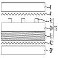
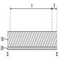
도 1b를 참조하면, 플렉서블 OLED 표시장치는 윈도우 커버(W)와 OLED 표시패널 사이에 형성되는 터치 센서를 포함한다.Referring to FIG. 1B, the flexible OLED display includes a touch sensor formed between the window cover W and the OLED display panel.
터치 센서는 일반적으로 터치된 부분을 감지하는 방식에 따라, 상판 또는 하판에 금속 전극을 형성하여 직류전압을 인가한 상태에서 터치된 위치를 저항에 따른 전압 구배(voltage gradient)로 판단하는 저항막 방식(resistive type), 도전막에 등전위를 형성하고 터치에 따른 상하판의 전압 변화가 일어난 위치를 감지하여 터치된 부분을 감지하는 정전용량 방식(capacitive type), 전자펜이 도전막을 터치함에 따라 유도되는 LC값을 읽어들여 터치된 부분을 감지하는 전자 유도 방식(electromagnetic type) 등으로 구별될 수 있으며, 그 외에도 광학 방식, 초음파 방식 등이 알려져 있다.A touch sensor is a resistance film type in which a metal electrode is formed on a top plate or a bottom plate in accordance with a method of sensing a touched portion and a touched position is judged as a voltage gradient according to a resistance in a state in which a DC voltage is applied a resistive type, a capacitive type in which an equal potential is formed on a conductive film and a touched portion is sensed by sensing a position where voltage changes of the upper and lower plates due to the touch are sensed, And an electromagnetic type in which the LC value is read to detect the touched portion. In addition, an optical method, an ultrasonic method, and the like are known.
이 중 요즘 시장에서 가장 많이 사용되는 정전용량 방식은 X축 전극패턴들과 Y축 전극패턴들을 교차시켜 매트릭스를 형성하고, 매트릭스 상의 임의의 위치에서 터치가 이루어지는 경우, 정전용량이 변화되는 매트릭스 상의 X축과 Y축의 좌표를 찾아내어 터치 위치를 검출하므로 접촉력이 작은 경우에도 터치위치를 감지할 수 있는 이점이 있다.The most widely used capacitive method in the market today is to form a matrix by crossing the X-axis electrode patterns and the Y-axis electrode patterns, and when a touch is made at an arbitrary position on the matrix, Axis and Y-axis are detected and the touch position is detected, there is an advantage that the touch position can be detected even when the contact force is small.
도 1b의 플렉서블 OLED에 적용된 터치 센서는 정정용량 방식 터치 센서이다.The touch sensor applied to the flexible OLED of Fig. 1B is a capacitive touch sensor.
도 1b를 참조하면, 터치 센서는 투명 기판(20) 상의 일면에 서로 나란하게 형성되는 복수의 터치 구동 전극들(Tx)과, 투명 기판(20)의 타면 상에 형성되며, 복수의 터치 구동전극들(Tx)과 교차하는 방향으로 나란하게 형성되는 복수의 터치 센싱 전극들(Rx)을 포함한다. 이와 같이 형성된 터치 센서의 상면(터치 센싱 전극들(RX)이 형성된 면)에는 제 1 접착제(A1)에 의해 윈도우 커버(W)가 부착되고, 터치 센서의 하면(터치 구동 전극들(.Tx)이 형성된 면)에는 제 2 접착제(A2)에 의해 표시장치(DP)가 부착된다.1B, the touch sensor includes a plurality of touch driving electrodes Tx formed on one surface of a transparent substrate 20 in parallel with each other, a plurality of touch driving electrodes Tx formed on the other surface of the transparent substrate 20, And a plurality of touch sensing electrodes Rx formed in parallel to each other in a direction intersecting the plurality of touch sensing electrodes Tx. The window cover W is attached to the upper surface of the touch sensor (the surface on which the touch sensing electrodes RX are formed) by the first adhesive A1 and the lower surface of the touch sensor (the touch driving electrodes Tx) The display device DP is attached by the second adhesive A2.
상술한 바와 같이 종래의 플렉서블 OLED 표시장치에 따르면 터치 센서는 접착제에 의해 OLED 표시장치에 상판부착(add on) 방식으로 부착된다.As described above, according to the conventional flexible OLED display device, the touch sensor is attached to the OLED display device in an add-on manner by an adhesive.
그러나, 이와 같이 상판부착 방식으로 플렉서블 OLED 표시장치에 터치 센서를 부착하면, 터치 센서의 추가로 인해 두께 및 무게, 그리고 제조 비용이 증가하는 등의 문제점이 있었다.
However, when the touch sensor is attached to the flexible OLED display device by the method of attaching the upper plate, there is a problem that thickness, weight, and manufacturing cost are increased due to the addition of the touch sensor.
본 발명은 상술한 종래의 문제점을 해소하기 위한 것으로, 플렉서블 OLED 표시장치의 구성요소를 이용함으로써 하여 플렉서블 OLED 표시장치의 두께와 무게를 줄이고 제조비용을 줄일 수 있는 플렉서블 OLED 표시장치 및 그 제조방법을 제공하는 것을 목적으로 한다.
SUMMARY OF THE INVENTION The present invention has been made in view of the above problems and it is an object of the present invention to provide a flexible OLED display device capable of reducing the thickness and weight of a flexible OLED display device and reducing manufacturing costs by using the components of the flexible OLED display device, The purpose is to provide.
상기 목적 달성을 위해 본 발명에 따르는 터치센서를 구비하는 유기 발광 다이오드 표시장치는, 유기 발광 다이오드와 상기 유기 발광 다이오드를 보호하기 위한 보호막이 형성된 기판과, 상기 기판 상에 형성되는 터치 센서를 구비하는 유기 발광 다이오드 표시장치로서, 상기 터치 센서는, 베이스층; 상기 베이스층의 제 1 면에서 제1 방향으로 형성되는 복수의 제 1 터치 전극들; 상기 베이스층의 제 1 면과 대향하는 제 2 면에서 상기 제 1 방향과 교차하는 제 2 방향으로 형성되는 복수의 제 2 터치 전극들; 상기 기판의 제 1 면에서 상기 복수의 제 1 전극들과 각각 연결된 복수의 제 1 라우팅 배선들; 상기 기판의 제 1 면에 형성되며 상기 복수의 제 1 라우팅 배선들과 분리된 복수의 제 2 라우팅 배선들; 및 상기 기판의 제 2 면에 형성되며, 상기 복수의 제 2 라우팅 배선들과 홀을 통해 각각 연결되는 복수의 제 3 라우팅 배선들을 포함하며, 상기 베이스층은 배리어층, 스크래치 방지층, 및 원 편광막 중의 적어도 하나인 것을 특징으로 한다.To achieve the above object, an organic light emitting diode display device having a touch sensor according to the present invention includes a substrate having an organic light emitting diode, a protective layer for protecting the organic light emitting diode, and a touch sensor formed on the substrate. An organic light emitting diode display device, comprising: a base layer; A plurality of first touch electrodes formed in a first direction on a first surface of the base layer; A plurality of second touch electrodes formed on a second surface of the base layer opposite to the first surface in a second direction intersecting with the first direction; A plurality of first routing interconnections each connected to the plurality of first electrodes on a first side of the substrate; A plurality of second routing lines formed on a first surface of the substrate and separated from the plurality of first routing lines; And a plurality of third routing interconnections formed on a second surface of the substrate and connected to the plurality of second routing interconnections through holes, respectively, the base layer comprising a barrier layer, a scratch resistant layer, Or the like.
상기 유기 발광 다이오드 표시장치는 상기 터치 센서 상부에 배치되는 원 편광막을 더 포함하며, 상기 베이스층은 상기 배리어층 및 상기 스크래치 방지층 중의 어느 하나인 것을 특징으로 한다.The organic light emitting diode display device may further include a circular polarizer film disposed on the touch sensor, wherein the base layer is one of the barrier layer and the scratch prevention layer.
상기 유기 발광 다이오드 표시장치는 상기 터치 센서 상부에 배열되는 선 편광막을 더 포함하며, 상기 베이스층은 상기 원 편광막인 것을 특징으로 한다.The organic light emitting diode display further includes a linear polarizer film arranged on the touch sensor, wherein the base layer is the circular polarizer film.
상기 터치 센서는 상기 베이스층과 상기 제 2 터치 전극들, 및 제 3 라우팅 배선들 사이에 형성되는 무기막을 더 포함할 수도 있다.The touch sensor may further include an inorganic film formed between the base layer, the second touch electrodes, and third routing wirings.
또한, 상기 홀은 상기 제 2 라우팅 배선, 상기 베이스층, 상기 제 3 라우팅 배선을 관통하는 관통홀일 수 있다.The hole may be a through hole passing through the second routing wiring, the base layer, and the third routing wiring.
또한, 상기 홀은 상기 제 2 라우팅 배선, 및 상기 베이스층을 관통하여 상기 제 3 라우팅 배선을 노출시키는 콘택홀 또는 상기 제 3 라우팅 배선 및 상기 베이스층을 관통하여 상기 제 2 라우팅 배선을 노출시키는 콘택홀일 수 있다.The hole is formed in the contact hole for exposing the third routing wiring through the second routing wiring and the base layer or the contact hole for exposing the second routing wiring through the third routing wiring and the base layer. Hole.
상기 터치 센서는 또한 상기 홀 내에 형성되어 상기 제 2 라우팅 배선과 상기 제 3 라우팅 배선을 연결하는 연결부를 더 포함할 수 있다.The touch sensor may further include a connection portion formed in the hole and connecting the second routing wiring and the third routing wiring.
상기 제 1 및 제 2 터치 전극들은 투명 도전층으로 형성되고, 상기 제 1, 제 2 및 제 3 라우팅 배선들은 투명 도전층과 금속층으로 형성된다.The first and second touch electrodes are formed of a transparent conductive layer, and the first, second, and third routing wirings are formed of a transparent conductive layer and a metal layer.
또한, 상기 목적달성을 위한 본 발명에 따르는 유기 발광 다이오드 표시장치 제조방법은, 기판 상에 유기 발광 다이오드와 상기 유기 발광 다이오드를 보호하기 위한 보호막을 형성하는 단계와 상기 보호막 상에 터치 센서를 형성하는 단계를 포함하는 유기 발광 다이오드 표시장치 제조방법으롯, 상기 터치 센서 형성단계는, 터치 전극 형성영역과 라우팅 배선 형성영역을 구비하는 베이스층을 준비하는 제 1 단계; 상기 베이스층의 제 1 면과 제 2 면에 각각 투명도전층과 금속층을 순차적으로 형성하는 제 2 단계; 포토리소그래피 공정을 이용하여 상기 제 1 면의 전극 형성영역에 투명 도전층으로 된 복수의 제 1 터치 전극을 형성하고, 제 1 면의 라우팅 배선 영역에 투명도전층과 금속층으로 되어 상기 복수의 제 1 터치전극들과 각각 연결되는 복수의 제 1 라우팅 배선들과, 상기 복수의 제 1 라우팅 배선들과 연결되지 않도록 복수의 제 2 라우팅 배선들을 형성하며, 상기 제 2 면의 전극 형성영역에 투명 도전층으로 된 복수의 제 2 터치 전극을 형성하고, 제 2 면의 라우팅 배선 영역에 투명도전층과 금속층으로 된 복수의 제 3 라우팅 배선들을 형성하는 제 3 단계; 상기 복수의 제 2 라우팅 배선들, 상기 베이스층, 및 상기 제 3 라우팅 배선들 중 상기 베이스층을 포함하는 적어도 2개를 관통하도록 홀을 형성하는 제 4 단계; 및 상기 홀에 금속물질을 채워 상기 제 2 라우팅 배선들을 상기 제 3 라우팅 배선들에 각각 연결하는 연결부들을 형성하는 제 5 단계를 포함한다.According to another aspect of the present invention, there is provided a method of manufacturing an organic light emitting diode display device, the method including forming an organic light emitting diode and a protective layer on the substrate, Wherein the step of forming the touch sensor includes the steps of: preparing a base layer having a touch electrode formation region and a routing wiring formation region; A second step of sequentially forming a transparent conductive layer and a metal layer on the first and second surfaces of the base layer, respectively; Forming a plurality of first touch electrodes made of a transparent conductive layer in an electrode formation region of the first surface by using a photolithography process; forming a transparent conductive layer and a metal layer in the routing wiring region of the first surface, A plurality of first routing wirings connected to the electrodes and a plurality of second routing wirings not connected to the plurality of first routing wirings, and a transparent conductive layer A third step of forming a plurality of second wiring lines made of a transparent conductive layer and a metal layer in a routing wiring region of a second surface; A fourth step of forming holes to penetrate at least two of the plurality of second routing wirings, the base layer, and the third routing wirings including the base layer; And a fifth step of filling the hole with a metal material to form connection portions connecting the second routing wires to the third routing wires, respectively.
또한, 상기 제 2 단계는 제 1 마스크를 이용한 포토리소그래피 공정으로 투명 도전층과 금속층으로 된 복수의 제 1 및 제 2 터치 전극들, 복수의 제 1 라우팅 배선들, 복수의 제 2 및 제 3 라우팅 배선들을 형성하는 단계; 및 제 2 마스크를 이용한 포토리소그래피 공정으로 투명 도전층으로 된 복수의 제 1 및 제 2 터치 전극들과, 투명 도전층과 금속층으로 된 복수의 제 1 라우팅 배선들, 복수의 제 2 및 제 3 라우팅 배선들을 형성하는 단계를 포함한다.In the second step, a plurality of first and second touch electrodes made of a transparent conductive layer and a metal layer, a plurality of first routing wiring lines, a plurality of second and third routing lines, and a plurality of second routing lines are formed by a photolithography process using a first mask. Forming wirings; A plurality of first and second touch electrodes made of a transparent conductive layer in a photolithography process using a second mask and a plurality of first routing wirings made of a transparent conductive layer and a metal layer, And forming wirings.
또한, 상기 제 1 단계 후, 상기 베이스층의 제 2 면에 무기막을 형성하는 단계를 더 포함하며, 상기 복수의 제 2 터치 전극들과, 상기 복수의 제 3 라우팅 배선들은 상기 무기막 상에 형성되는 것을 특징으로 한다.The method may further include forming an inorganic film on the second surface of the base layer after the first step, wherein the plurality of second touch electrodes and the plurality of third routing interconnections are formed on the inorganic film .
상기 제 1 단계 후, 상기 홀들은 레이저 드릴 방법(laser drill method), CNC (Computerized Numerical Control) 드릴 방법, 펀칭(punching) 방법 중 어느 하나의 방법으로 형성될 수 있다.After the first step, the holes may be formed by any one of a laser drill method, a CNC (drilling method), and a punching method.
또한, 상기 연결부들은 스크린 프린팅 방법(screen printing method), 디스펜스 방법(dispense method), 잉크젯 방법(inkjet method), 전기 도금 방법 중 어느 하나의 방법에 의해 형성될 수 있다.
The connection portions may be formed by any one of a screen printing method, a dispense method, an inkjet method, and an electroplating method.
본 발명에 따르면, 터치 센서의 베이스층이 플렉서블 OLED의 배리어층(barrier layer), 스크래치 방지층, 원 편광막(circular polarization film) 중의 적어도 하나의 기능을 겸하기 때문에 이 터치 센서를 플렉서블 OLED 표시장치에 적용하면, 플렉서블 OLED 표시장치의 두께와 무게를 줄임과 동시에 제조비용을 줄일 수 있는 효과를 얻을 수 있다.According to the present invention, since the base layer of the touch sensor also functions as at least one of the barrier layer of the flexible OLED, the anti-scratch layer, and the circular polarization film, the touch sensor can be applied to the flexible OLED display The effect of reducing the thickness and weight of the flexible OLED display device and reducing the manufacturing cost can be obtained.
도 1a는 종래의 플렉서블 OLED 표시장치의 구성을 개략적으로 도시한 단면도이다.
도 1b는 터치 센서를 구비하는 종래의 플렉서블 OLED 표시장치의 구성을 개략적으로 도시한 단면도이다.
도 2는 본 발명의 실시예에 따른 터치 센서를 구비하는 플렉서브 OLED 표시장치의 구성을 도시한 단면도이다.
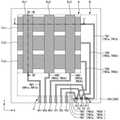
도 3은 도 2에 도시된 터치 센서(TS)를 도시한 평면도이다.
도 4a는 도 3에 도시된 라인 I-I'및 II-II'을 따라 취한 단면도이다.
도 4b는 도 3의 라인 III-III'을 따라 취한 단면도이다.
도 5는 본 발명의 실시예에 따른 터치센서를 제조하기 위한 제 1 공정을 도시한 평면도이다.
도 6a는 도 5의 라인 I-I' 및 II-II'을 따라 취한 단면도이다.
도 6b는 도 5의 라인 III-III'을 따라 취한 단면도이다.
도 7은 본 발명의 실시예에 따른 터치센서를 제조하기 위한 제 2 공정을 도시한 평면도이다.
도 8a는 도 7의 라인 I-I' 및 II-II'을 따라 취한 단면도이다.
도 8b는 도 7의 라인 III-III'을 따라 취한 단면도이다.
도 9는 본 발명의 실시예에 따른 터치센서를 제조하기 위한 제 3 공정을 도시한 평면도이다.
도 10a는 도 9의 라인 I-I' 및 II-II'을 따라 취한 단면도이다.
도 10b는 도 9의 라인 III-III'을 따라 취한 단면도이다.
도 11은 본 발명의 실시예에 따른 터치센서를 제조하기 위한 제 4 공정을 도시한 평면도이다.
도 12a는 도 11의 라인 I-I' 및 II-II'을 따라 취한 단면도이다.
도 12b는 도 11의 라인 III-III'을 따라 취한 단면도이다.1A is a cross-sectional view schematically showing the structure of a conventional flexible OLED display device.
1B is a cross-sectional view schematically showing the structure of a conventional flexible OLED display device having a touch sensor.
2 is a cross-sectional view illustrating a structure of a PLL sub-OLED display device having a touch sensor according to an embodiment of the present invention.
3 is a plan view showing the touch sensor TS shown in Fig.
4A is a cross-sectional view taken along lines I-I 'and II-II' shown in FIG. 3;
FIG. 4B is a cross-sectional view taken along line III-III 'of FIG. 3; FIG.
5 is a plan view showing a first process for manufacturing a touch sensor according to an embodiment of the present invention.
FIG. 6A is a cross-sectional view taken along lines II 'and II-II' of FIG. 5; FIG.
FIG. 6B is a cross-sectional view taken along line III-III 'of FIG. 5; FIG.
7 is a plan view showing a second process for manufacturing a touch sensor according to an embodiment of the present invention.
FIG. 8A is a cross-sectional view taken along lines II 'and II-II' of FIG. 7; FIG.
FIG. 8B is a cross-sectional view taken along line III-III 'of FIG. 7. FIG.
9 is a plan view showing a third process for manufacturing a touch sensor according to an embodiment of the present invention.
10A is a cross-sectional view taken along lines II 'and II-II' of FIG.
10B is a cross-sectional view taken along line III-III 'of FIG.
11 is a plan view showing a fourth step for manufacturing a touch sensor according to an embodiment of the present invention.
12A is a cross-sectional view taken along lines II 'and II-II' of FIG.
12B is a cross-sectional view taken along the line III-III 'of FIG.
이하, 첨부 도면을 참조하여 본 발명에 따른 바람직한 실시예들을 상세히 설명한다. 명세서 전체에 걸쳐서 동일한 참조번호들은 실질적으로 동일한 구성요소들을 의미한다.Hereinafter, preferred embodiments according to the present invention will be described in detail with reference to the accompanying drawings. Like reference numerals throughout the specification denote substantially identical components.
이하, 본 발명의 실시예에 따른 OLED 표시장치를 도 2 내지 도 도 4b를 참조하여 보다 상세히 설명한다.Hereinafter, an OLED display according to an embodiment of the present invention will be described in detail with reference to FIGS. 2 to 4B. FIG.
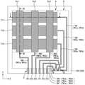
도 2는 본 발명의 실시예에 따른 터치 센서를 구비하는 플렉서브 OLED 표시장치의 구성을 도시한 단면도이고, 도 3은 도 2에 도시된 터치 센서(TS)를 도시한 평면도이며, 도 4a는 도 3에 도시된 라인 I-I' 및 II-II'을 따라 취한 단면도이고, 도 4b는 도 3의 라인 III-III'을 따라 취한 단면도이다.FIG. 3 is a plan view showing the touch sensor TS shown in FIG. 2, and FIG. 4A is a cross-sectional view of the touch sensor according to the first embodiment of the present invention. Sectional view taken along lines II 'and II-II' shown in FIG. 3, and FIG. 4b is a sectional view taken along line III-III 'shown in FIG.
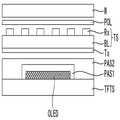
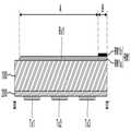
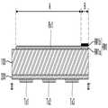
도 2를 참조하면, 본 발명의 실시예에 따르는 OLED 표시장치는 데이터 라인들, 게이트 라인들 및 박막 트랜지스터 등의 표시소자(도시생략)가 형성된 박막 트랜지스터 기판(TFTA)과, TFT 기판(TFTA) 상에 형성되는 유기 발광다이오드(OLED)(11)와, 유기 발광 다이오드를 감싸도록 형성되어 외부로부터 산소나 수분이 침투하는 것을 방지하기 위한 제 1 보호막(PAS1), 제 1 보호막(PAS1) 상에 형성되어 외부로부터 산소나 수분이 침투하는 것을 방지하기 위한 제 2 보호막(PAS2), 제 2 보호막(PAS2) 상에 형성되는 터치 센서(TS), 터치 센서 상부에 배치되어 투과광을 일정 방향으로 통과시키는 편광막(POL), 및 편광막(POL) 상에 배치되어 터치 센서를 보호하기 위한 윈도우 커버(W)를 포함한다.2, an OLED display according to an embodiment of the present invention includes a thin film transistor substrate (TFTA) having display lines (not shown) such as data lines, gate lines and thin film transistors formed thereon, a TFT substrate (TFTA) A first passivation layer PAS1 formed to surround the organic light emitting diode and preventing oxygen or moisture from penetrating from the outside, a first passivation layer PAS1 formed on the first passivation layer PAS1, A second protective film PAS2 for preventing penetration of oxygen or moisture from the outside, a touch sensor TS formed on the second protective film PAS2, and a touch sensor TS disposed on the touch sensor for passing the transmitted light in a predetermined direction A polarizing film POL, and a window cover W disposed on the polarizing film POL to protect the touch sensor.
터치 센서(TS)는 베이스층(BL)과 그 상하부에 각각 형성되는 제 1 터치전극들(Rx1~Rx3) 및 터치 구동전극들(Tx)을 포함한다.The touch sensor TS includes a base layer BL and first touch electrodes Rx1 to Rx3 and touch driving electrodes Tx formed on upper and lower portions thereof.
도 3 및 도 4a, 도 4b를 참조하면, 본 발명의 실시예에 따른 터치 센서(TS)는 터치 전극들이 형성되는 터치전극 형성영역(A), 터치 전극들과 각각 접속되는 라우팅 배선들이 형성되는 라우팅 배선 형성영역(B) 및 라우팅 배선들과 터치 구동회로의 신호라인들을 연결하기 위한 라우팅 패드들이 형성되는 패드 형성영역(C)을 포함한다.3 and 4A and 4B, the touch sensor TS according to the embodiment of the present invention includes a touch electrode formation area A where touch electrodes are formed, and routing wires connected to the touch electrodes, respectively And a pad formation region (C) in which routing pads for connecting the routing wiring formation region (B) and the signal lines of the touch driving circuit with the routing wirings are formed.
전극 형성부(A)는 베이스층(100)의 일면 상에 형성되는 복수의 제 1 터치 전극들(Rx1~Rx3)과, 베이스층(100)의 타면에서 무기막(200)을 사이에 두고 상기 복수의 제 1 전극들(Rx)과 교차하도록 형성되는 복수의 제 2 터치 전극들(Tx1~Tx3)을 포함한다.The electrode forming portion A includes a plurality of first touch electrodes Rx1 to Rx3 formed on one surface of the
제 1 터치 전극들(Rx1~Rx3)은 베이스층(100)의 일면(예를 들면, 상면)에 형성되며, 제 1 방향(예컨대, Y축 방향)으로 서로 나란하게 배열된다. 복수의 제 2 터치 전극들(Tx1~Tx3)은 베이스층(100)의 타면(예를 들면, 하면)에 형성된 무기막(200)에 형성되며, 상기 제 1 터치 전극들(Rx1~Rx3)과 교차하는 제 2 방향(예컨대, X축 방향)으로 서로 나란하게 배열된다. 이처럼, 제 1 및 제 2 전극들(Rx1~Rx3, Tx1~Tx3)은 베이스층(100) 및 무기막(200)을 사이에 두고, 서로 교차되도록 배열되어 있으므로 서로 절연상태를 유지한다.The first touch electrodes Rx1 to Rx3 are formed on one surface (e.g., an upper surface) of the
본 발명의 실시예에 따른 터치 센서에서 베이스층(100)은 폴리카보네이트(Poly Carbonate; PC), 사이클로 올레핀 폴리머(Cyclo Olefin Polymer; COP)처럼 연신되지 않은 광등방성 필름으로 형성된다.In the touch sensor according to the embodiment of the present invention, the
또한, 본 발명의 실시예에 따른 터치 센서(TS)의 베이스층(100)은 OLED 표시장치의 산소나 수분 침투의 방지를 위한 배리어층(barrier layer), 스크래치 방지층, 원 편광막(circular polarization film) 중의 적어도 하나의 기능을 겸할 수 있다. 다만, 터치 센서(Ts)의 베이스층(BL)이 배리어층 또는 스크래치 방지층의 기능을 겸할 경우, 도 2에 도시된 편광막(POL)은 원 편광막이 되며, 원 편광막의 기능을 겸할 경우, 도 2에 도시된 편광막은 선 편광막(linear polarization film)이 된다.In addition, the
제 1 및 제 2 터치 전극들(Rx1~Rx3, Tx1~Tx3)은 ITO(Indium Tin Oxide), IZO(Indium Zinc Oxide), GZO(Gallium-doped Zinc Oxide), 금속 메쉬형(metal mesh type) 투명 전극, 금속 나노와이어(metal nanowire), 또는 탄소 계열 투명 전극들과 같은 투명 도전성 물질로 형성된다.The first and second touch electrodes Rx1 to Rx3 and Tx1 to Tx3 are formed of indium tin oxide (ITO), indium zinc oxide (IZO), gallium-doped zinc oxide (GZO) Electrode, a metal nanowire, or a carbon-based transparent electrode.
베이스층(100)의 하면에 형성된 무기막(200)은 실리콘 산화물(SiO2), 실리콘 질화물(SiNx), 실리콘 산화질화물(SiOxNy), 알루미늄 산화물(AlOx), 알루미늄 질화물(AlNx), 산화 티타늄(TIO2), 산화아연(ZnO)과 같은 물질로 형성된다.
라우팅 배선 형성영역(B)은 베이스층(100)의 전극 형성영역(A) 외곽에 형성되는 복수의 제 1 라우팅 배선들(RW1~RW3)과, 복수의 제 2 라우팅 배선들(TW1'~TW3')과, 복수의 제 3 라우팅 배선들(TW1~TW3)과, 복수의 홀들(holes)(H1~H3)과, 상기 홀(H1~H3)들을 통해 상기 복수의 제 2 라우팅 배선들(TW1'~TW3')과 복수의 제 3 라우팅 배선들(TW1~TW3)을 각각 연결하는 복수의 연결부들(C1~C3)을 포함한다.The routing wiring formation region B includes a plurality of first routing wirings RW1 to RW3 formed outside the electrode formation region A of the
복수의 제 1 라우팅 배선들(RW1~RW3)은 제1 터치 전극들(Rx1~Rx3)로부터 각각 연장되는 제1층들(RW1a~RW3a)과, 상기 제1층들(RW1a~RW3a) 상에 각각 형성되는 제2층들(RW1b~RW3b)의 이중층(double layer)으로 형성된다.The plurality of first routing wirings RW1 to RW3 are respectively formed on the first layers RW1a to RW3a extending from the first touch electrodes Rx1 to Rx3 and the first layers RW1a to RW3a, Is formed as a double layer of the second layers RW1b to RW3b.
복수의 제 2 라우팅 배선들(TW1'~TW3')은 각각 복수의 홀들(H1~H3)에 채워진 복수의 연결부(C1~C3)에 의해 복수의 제 3 라우팅 배선들(TW1~TW3)에 접속되며, 제1층들(TW1a'~TW3a')과, 상기 제1층들(TW1a'~TW3a') 상에 각각 형성되는 제2층들(TW1b'~TW3b')의 이중층(double layer)으로 형성된다.The plurality of second routing wirings TW1 'to TW3' are connected to the plurality of third routing wirings TW1 to TW3 by the plurality of connection portions C1 to C3 filled in the plurality of holes H1 to H3, respectively And is formed of a double layer of first layers TW1a 'to TW3a' and second layers TW1b 'to TW3b' formed on the first layers TW1a 'to TW3a', respectively.
복수의 제 3 라우팅 배선들(TW1~TW3)은 제 2 터치 전극들(Tx1~Tx3)로부터 각각 연장되는 제1층들(TW1a~TW3a)과, 상기 제1층들(TW1a~TW3a) 상에 각각 형성되는 제2층들(TW1b~TW3b)의 이중층(double layer)으로 형성된다.The plurality of third routing wirings TW1 to TW3 are respectively formed on the first layers TW1a to TW3a extending from the second touch electrodes Tx1 to Tx3 and the first layers TW1a to TW3a respectively, Is formed as a double layer of the second layers (TW1b to TW3b).
상술한 바와 같이, 제 1, 제 2 및 제 3 라우팅 배선들(RW1~RW3, TW1'~TW3', TW1~TW3)의 각각은 제1층(RW1a~RW3a, TW1a'~TW3a', TW1a~TW3a)과 제2층(RW1b~RW3b, TW1b'~TW3b', TW1b~TW3b)의 2층 구조로 이뤄져 있다. 이중 제1층(RW1a~RW3a, TW1a'~TW3a', TW1a~TW3a)은 투명 금속층으로서, ITO(Indium Tin Oxide), IZO(Indioum Zinc Oxide), GZO(Gallium-doped Zinc Oxide), 금속 메쉬형(metal mesh type) 투명 전극, 금속 나노와이어(metal Nano Wire), 또는 탄소 계열 투명 전극들과 같은 투명 도전성 물질로 형성되고, 제 2 층(RW1b~RW3b, TW1b'~TW3b', TW1b~TW3b)은 Al, AlNd, Mo, MoTi, Cu, Cr, Ag, Ag 계열 합금들과 같은 금속물질로 형성된다.As described above, each of the first, second, and third routing wirings RW1 to RW3, TW1 'to TW3', and TW1 to TW3 includes first layers RW1a to RW3a and TW1a 'to TW3a' Layer structure of the second layer (RW1b to RW3b, TW1b 'to TW3b', TW1b to TW3b). The first layer (RW1a to RW3a, TW1a 'to TW3a', TW1a to TW3a) is formed of a transparent metal layer such as ITO (Indium Tin Oxide), IZO (Indium Zinc Oxide), GZO (Gallium-doped Zinc Oxide) (RW1b to RW3b, TW1b 'to TW3b', TW1b to TW3b) formed of a transparent conductive material such as a metal mesh type transparent electrode, a metal nano wire, or a carbon-based transparent electrode, Is formed of a metal material such as Al, AlNd, Mo, MoTi, Cu, Cr, Ag, or Ag-based alloys.
본 발명의 실시예에서 복수의 홀들(H1~H3)은 복수의 제 2 라우팅 배선들(TW1'~TW3'), 베이스층(100), 무기막(200), 및 복수의 제 3 라우팅 배선들(TW1~TW3)의 각각을 관통하도록 형성되는 관통홀들(through holes)의 형태로 형성되었다. 그러나, 본 발명이 이에 한정되는 것은 아니며, 복수의 홀들(H1~H3)은 복수의 제 2 라우팅 배선들(TW1'~TW3'), 베이스층(100) 및 무기막(200)을 관통하여 복수의 제 3 라우팅 배선들(TW1~TW3)이 노출되도록 하거나, 또는 복수의 제 3 라우팅 배선들(TW1~TW3), 무기막(200), 및 베이스층(100)을 관통하여 복수의 제 2 라우팅 배선들(TW1'~TW3')이 노출되도록 하는 콘택홀들(contact holes)의 형태로 형성될 수도 있다.In the embodiment of the present invention, the plurality of holes H1 to H3 include a plurality of second routing wirings TW1 'to TW3', a
복수의 연결부들(C1~C3)은 상기 복수의 홀들(H1~H3)에 각각 채워져 무기막(200)상에 형성된 복수의 제 2 라우팅 배선들(TW1'~TW3')과 베이스층(100)의 일면에 형성된 복수의 제 3 라우팅 배선들(TW1~TW3)을 각각 연결한다. 연결부들(C1~C3)은 Al, AlNd, Mo, MoTi, Cu, Cr, Ag, Ag 계열 합금과 같은 금속물질로 형성된다.The plurality of connection portions C1 to C3 are filled in the plurality of holes H1 to H3 to form a plurality of second routing wirings TW1 'to TW3' formed on the
패드 형성부(C)는 베이스층(100)의 라우팅 배선부(B)에 인접하여 형성되는 복수의 제 1 라우팅 패드들(RP1~RP3)과, 복수의 제 2 라우팅 패드들(TP1~TP3)을 포함한다.The pad forming portion C includes a plurality of first routing pads RP1 to RP3 formed adjacent to the routing wiring portion B of the
복수의 제 1 라우팅 패드들(RP1~RP3)은 각각 복수의 제 1 라우팅 배선들(RW1~RW3)을 통해 복수의 제 1 터치 전극들(Rx1~Rx3)에 각각 접속되고, 복수의 제 2 라우팅 패드들(TP1~TP3)은 각각 복수의 제 2 라우팅 배선들(TW1'~TW3'), 복수의 연결부들(C1~C3), 및 복수의 제 3 라우팅 배선들(TW1~TW3)을 통해 복수의 제 2 터치 전극들(Tx1~Tx3)에 각각 접속된다. 제 1 및 제 2 라우팅 패드들(RP1~RP3, TP1~TP3) 또한 라우팅 배선들과 마찬가지로 투명 도전성 물질로 된 제1층과 금속물질로 된 제2층 의 2층 구조로 형성된다.The plurality of first routing pads RP1 to RP3 are respectively connected to the plurality of first touch electrodes Rx1 to Rx3 through a plurality of first routing wirings RW1 to RW3, The pads TP1 to TP3 are respectively connected to a plurality of second routing wirings TW1 'to TW3', a plurality of connection portions C1 to C3 and a plurality of third routing wirings TW1 to TW3, The second touch electrodes Tx1 to Tx3, respectively. The first and second routing pads RP1 to RP3 and TP1 to TP3 are also formed in a two-layer structure of a first layer made of a transparent conductive material and a second layer made of a metal material, similar to the routing wiring.
이하, 도 5 내지 도 12b를 참조하여 본 발명의 실시예에 따르는 터치 센서(TS)의 제조방법에 대해서 설명한다.Hereinafter, a method of manufacturing the touch sensor TS according to the embodiment of the present invention will be described with reference to FIGS. 5 to 12B. FIG.
우선, 도 5, 도 6a, 및 도 6b를 참조하여 베이스층(100)에 무기막(200)을 형성하는 공정에 대해 설명하기로 한다. 도 5는 본 발명의 실시예에 따른 터치 센서를 제조하기 위한 제 1 공정을 도시한 평면도이고, 도 6a는 도 5의 라인 I-I' 및 II-II'을 따라 취한 단면도이며, 도 6b는 도 5의 라인 III-III'을 따라 취한 단면도이다.First, the process of forming the
도 5, 도 6a, 및 도 6b를 참조하면, 폴리카보네이트(Poly Carbonate; PC), 사이클로 올레핀 폴리머(Cyclo Olefin Polymer; COP)처럼 연신되지 않은 광등방성 필름으로 형성된 베이스층(100)의 일면 상에 스퍼터링법(sputtering)법과 같은 증착법을 이용하여 실리콘 산화막(SiO2), 실리콘 질화막(SiNx), 실리콘 산화질화막(SiON), 알루미늄 산화물(AlOx), 질화 알루미늄(AlNx), 산화 티타늄(TiO2), 산화아연(ZnO)과 같은 물질로부터 선택된 무기막(200)이 형성된다.Referring to FIGS. 5, 6A and 6B, on one side of a
다음으로, 도 7, 도 8a, 및 도 8b를 참조하여 제 1 및 제 2 터치 전극들, 제 1 및 제 2 터치 라우팅 배선들, 및 제 1 및 제 2 라우팅 패드들을 형성하는 공정에 대해 설명하기로 한다. 도 7은 도 7은 본 발명의 실시예에 따른 터치 센서를 제조하기 위한 제 2 공정을 도시한 평면도이고, 도 8a는 도 7의 라인 I-I' 및 II-II'을 따라 취한 단면도이며, 도 8b는 도 7의 라인 III-III'을 따라 취한 단면도이다.Next, the process of forming the first and second touch electrodes, the first and second touch routing wirings, and the first and second routing pads will be described with reference to Figs. 7, 8A, and 8B . FIG. 7 is a plan view showing a second process for manufacturing a touch sensor according to an embodiment of the present invention, FIG. 8A is a sectional view taken along lines II 'and II-II' of FIG. 7, and FIG. Is a cross-sectional view taken along the line III-III 'in FIG.
도 7, 도 8a, 및 도 8b를 참조하면, 베이스층(100)의 일면과 베이스층(100)의 타면에 형성된 무기막(200) 상에 각각 투명 도전층과 금속층을 순차적으로 형성된 후 이를 패터닝하여, 복수의 제 1 및 제 2 터치 전극들(Rx1~Rx3, Tx1~Tx3), 복수의 제 1 라우팅 배선들(RW1~RW3), 복수의 제 2 및 제 3 라우팅 배선들(TW1'~TW3' TW1~TW3), 및 복수의 제 1 및 제 2 라우팅 패드들(RP1~RP3, TP1~TP3)이 형성된다.Referring to FIGS. 7, 8A, and 8B, a transparent conductive layer and a metal layer are sequentially formed on one side of the
보다 구체적으로 설명하면, PECVD(a plasma-enhanced chemical vapor deposition) 등의 증착공정을 이용하여 베이스층(100)의 일면 상과 베이스층(100)의 타면에 형성된 무기막(200) 상에 각각 투명 도전층과 금속층이 순차적으로 증착된다.More specifically, on the
다음으로, 베이스층(100) 상의 금속층과 무기막(200) 상의 금속층 상에 각각 포토레지스트를 전면 도포한다. 그리고, 제 1 마스크를 이용한 포토리소그래피 공정을 이용하여, 베이스층(100) 상에 제 1 포토레지스트 패턴(도시생략)을 형성하고, 제 2 마스크를 이용한 포토리소그래피 공정을 이용하여 무기막(200) 상에 제 2 포토레지스트 패턴(도시생략)을 형성한다. 제 1 포토레지스트 패턴은 복수의 제 1 터치 전극들(Rx1~Rx3), 복수의 제 1 라우팅 배선들(RW1~RW3), 복수의 제 2 라우팅 배선들(TW1'~TW3'), 및 복수의 제 1 및 제 2 라우팅 패드들(RP1~RP3, TP1~TP3)이 형성될 영역을 제외한 베이스층(100) 상의 금속층을 노출시킨다. 제 2 포토레지스트 패턴은 복수의 제 2 터치 전극들(Tx1~Tx3)과 복수의 제 3 라우팅 배선들(TW1~TW3)이 형성될 영역을 제외한 무기막(200) 상의 금속층을 노출시킨다.Next, the photoresist is entirely coated on the metal layer on the
제 1 포토레지스트 패턴을 통해 노출된 베이스층(100) 상의 금속층 및 투명 도전층을 에칭으로 제거한 후, 금속층 상에 잔류하는 제 1 포토레지스트 패턴을 제거하면, 투명 도전층과 금속층으로 된 2중층(double layer) 구조의 복수의 제 1 터치 전극들(Rx1~Rx3), 복수의 제 1 라우팅 배선들(RW1~RW3), 복수의 제 2 라우팅 배선들(TW1'~TW3'), 및 복수의 제 1 및 제 2 라우팅 패드들(RP1~RP3, TP1~TP3)이 베이스층(100) 상에 형성된다.After the metal layer and the transparent conductive layer on the
또한, 제 2 포토레지스트 패턴을 통해 노출된 무기막(200) 상의 금속층 및 투명 도전층을 에칭으로 제거한 후, 금속층 상에 잔류하는 제 2 포토레지스트 패턴을 제거하면, 투명 도전층과 금속층으로 된 2중층(double layer) 구조의 복수의 제 2 터치 전극들(Tx1~Tx3)과 복수의 제 3 라우팅 배선들(TW1~TW3)이 무기막(200) 상에 형성된다.When the metal layer and the transparent conductive layer on the
결과적으로, 복수의 제 1 터치 전극들(Rx1~Rx3), 복수의 제 1 라우팅 배선들(RW1~RW3), 복수의 제 2 라우팅 배선들(TW1'~TW3'), 및 복수의 제 1 및 제 2 라우팅 패드들(RP1~RP3, TP1~TP3)은 베이스층(100)의 일면 상에 형성되고, 제 2 터치 전극들(Tx1~Tx3), 및 복수의 제 3 라우팅 배선들(TW1~TW3)은 베이스층(100)의 타면 상에 형성된 무기막(200)에 형성된다.As a result, a plurality of first touch electrodes Rx1 to Rx3, a plurality of first routing wirings RW1 to RW3, a plurality of second routing wirings TW1 'to TW3' The second routing pads RP1 to RP3 and TP1 to TP3 are formed on one surface of the
다음으로, 복수의 제 1 터치 전극들(RX1~Rx3), 복수의 제 1 라우팅 배선들(RW1~RW3), 복수의 제 2 라우팅 배선들(TW1'~TW3'), 및 복수의 제 1 및 제 2 라우팅 패드들(RP1~RP3, TP1~TP3)이 형성된 베이스층(100)과, 복수의 제 2 터치 전극들(Tx1~Tx3) 및 복수의 제 3 라우팅 배선들(TW1~TW3)이 형성된 무기막(200) 상에 각각 포토레지스트를 전면 도포한다. 그리고, 제 3 마스크를 이용한 포토리소그래피 공정을 이용하여 이중층의 복수의 제 1 터치 전극들(Rx1~Rx3)이 형성된 베이스층(100) 상에 제 3 포토레지스트 패턴(도시생략)을 형성하고, 제 4 마스크를 이용한 포토리소그래피 공정을 이용하여 이중층의 복수의 제 2 터치 전극들(Tx1~Tx3)이 형성된 무기막(200) 상에 제 4 포토레지스트 패턴(도시생략)을 형성한다. 제 3 포토레지스트 패턴은 2중층의 제 1 터치 전극들(Rx1~Rx3)을 노출시키고, 제 4 포토레지스트 패턴은 2중층의 제 2 터치 전극들(Tx1~Tx3)을 노출시킨다.Next, a plurality of first touch electrodes RX1 to Rx3, a plurality of first routing wirings RW1 to RW3, a plurality of second routing wirings TW1 'to TW3' A
그리고, 제 3 포토레지스트 패턴을 통해 노출된 2중층의 제 1 터치 전극들(Rx1~Rx3)의 금속층을 에칭으로 제거한 후, 잔류하는 제 3 포토레지스트 패턴을 제거하면, 투명 도전층으로 된 복수의 제 1 터치 전극들(RX1~Rx3)이 베이스층(100)의 터치 전극 형성영역(A)에 형성된다.After the metal layer of the first touch electrodes Rx1 to Rx3 of the double layer exposed through the third photoresist pattern is removed by etching and the remaining third photoresist pattern is removed, The first touch electrodes RX1 to RX3 are formed in the touch electrode formation area A of the
또한, 제 4 포토레지스트 패턴을 통해 노출된 2중층의 제 2 터치 전극들(Tx1~Tx3)의 금속층을 에칭으로 제거한 후, 잔류하는 제 4 포토레지스트 패턴을 제거하면, 투명 도전층으로 된 복수의 제 2 터치 전극들(Tx1~Tx3)이 무기막(200)의 터치 전극 형성영역(A)에 형성된다.When the remaining metal layer of the second touch electrodes Tx1 to Tx3 exposed through the fourth photoresist pattern is removed by etching and the remaining fourth photoresist pattern is removed, a plurality of The second touch electrodes Tx1 to Tx3 are formed in the touch electrode formation area A of the
한편, 베이스층(100)의 라우팅 배선 형성영역(B)에는 2층 구조의 복수의 제 1 라우팅 배선들(RW1~RW3) 및 복수의 제 2 라우팅 배선들(TW1'~TW3')이 형성되고, 무기막(200)의 라우팅 배선 형성영역(B)에는 2층 구조의 복수의 제 3 라우팅 배선들(TW1~TW3)이 형성된다. 또한, 베이스층(100)의 패드 형성영역(C)에는 2층 구조의 복수의 제 1 및 제 2 라우팅 패드들(RP1~RP3, TP1~TP3)이 형성된다.On the other hand, a plurality of first routing wirings RW1 to RW3 and a plurality of second routing wirings TW1 'to TW3' having a two-layer structure are formed in the routing wiring formation area B of the
투명 도전층은 ITO(Indium Tin Oxide), IZO(Indioum Zinc Oxide), GZO(Gallium-doped Zinc Oxide), 금속 메쉬형 투명 전극, 금속 나노 와이어, 탄소 계열 투명 전극들 같은 투명 도전성 물질로 형성되고, 금속층은 Al, AlNd, Mo, MoTi, Cu, Cr, Ag, Ag 계열 합금들과 같은 금속물질로 형성된다.The transparent conductive layer is formed of a transparent conductive material such as indium tin oxide (ITO), indium zinc oxide (IZO), gallium-doped zinc oxide (GZO), metal mesh type transparent electrode, metal nanowire, The metal layer is formed of a metal material such as Al, AlNd, Mo, MoTi, Cu, Cr, Ag, Ag series alloys.
이상의 설명에서는 복수의 제 1 및 제 2 터치 전극들(Rx1~Rx3, Tx1~Tx3), 복수의 제 1 라우팅 배선들(RW1~RW3), 복수의 제 2 및 제 3 라우팅 배선들(TW1'~TW3', TW1~TW3), 및 복수의 제 1 및 제 2 라우팅 패드들(RP1~RP3, TP1~TP3)을 형성하기 위해 2개의 마스크가 이용되는 예를 설명했지만, 하프톤 마스크를 사용하면, 하나의 마스크 공정으로도 실시 가능하다. 하프톤 마스크 공정은 당업계에 알려져 있는 공지의 기술이므로, 여기에서는 그에 대한 설명은 생략하기로 한다.In the above description, a plurality of first and second touch electrodes Rx1 to Rx3, Tx1 to Tx3, a plurality of first routing wirings RW1 to RW3, a plurality of second and third routing wirings TW1 ' TW3 ', TW1 to TW3) and two masks are used to form the plurality of first and second routing pads (RP1 to RP3, TP1 to TP3), but using a halftone mask, It is also possible to use a single mask process. Since the halftone mask process is a well-known technique known in the art, a description thereof will be omitted here.
다음으로, 도 9, 도 10a, 및 도 10b를 참조하여 라우팅 배선 형성영역(B)에 복수의 홀들을 형성하는 제 3 공정에 대해 설명하기로 한다. 도 9는 도 7은 본 발명의 실시예에 따른 터치 센서를 제조하기 위한 제 3 공정을 도시한 평면도이고, 도 10a는 도 9의 라인 I-I' 및 II-II'을 따라 취한 단면도이며, 도 10b는 도 9의 라인 III-III'을 따라 취한 단면도이다.Next, a third process for forming a plurality of holes in the routing wiring formation region B will be described with reference to Figs. 9, 10A, and 10B. FIG. 9 is a plan view showing a third process for manufacturing a touch sensor according to an embodiment of the present invention, FIG. 10A is a cross-sectional view taken along lines II 'and II-II' of FIG. 9, Is a cross-sectional view taken along the line III-III 'in FIG.
도 9, 도 10a, 및 도 10b를 참조하면, 제 2 라우팅 배선들(TW1'~TW3'), 베이스층(100), 무기막(200), 및 제 3 라우팅 배선들(TW1~TW3)을 각각 관통하는 복수의 홀들(H1~H3)이 형성된다. 복수의 홀들(H1~H3)은 포토리소그래피 공정을 통해 형성될 수 있지만, 바람직하게는 레이저 드릴 방법(laser drill method), CNC (Computerized Numerical Control) 드릴 방법, 펀칭(punching) 방법 등을 이용하여 형성된다.Referring to FIGS. 9, 10A and 10B, the second routing wirings TW1 'to TW3', the
본 발명의 실시예에서, 상기 복수의 홀들(H1~H3)은 관통홀(through holes)의 형태로 형성되었다. 그러나, 본 발명이 이에 한정되는 것은 아니며, 복수의 홀들(H1~H3)은 복수의 제 2 라우팅 배선들(TW1'~TW3'), 베이스층(100) 및 무기막(200)을 관통하여 복수의 제 3 라우팅 배선들(TW1~TW3)이 노출되도록 하거나, 또는 복수의 제 3 라우팅 배선들(TW1~TW3), 무기막(200), 및 베이스층(100)을 관통하여 복수의 제 2 라우팅 배선들(TW1'~TW3')이 노출되도록 하는 콘택홀들(contact holes)의 형태로 형성될 수도 있다.In the embodiment of the present invention, the plurality of holes H1 to H3 are formed in the form of through holes. However, the present invention is not limited thereto, and the plurality of holes H1 to H3 may be formed by penetrating the plurality of second routing wirings TW1 'to TW3', the
다음으로, 도 11, 도 12a, 및 도 12b를 참조하여 복수의 제 2 라우팅 배선들(TW1'~TW3')과 복수의 제 3 라우팅 배선들(TW1~TW3)를 각각 연결하는 복수의 연결부들(C1~C3)을 형성하는 공정에 대해 설명하기로 한다. 도 11은 본 발명의 실시예에 따른 터치 센서를 제조하기 위한 제 4 공정을 도시한 평면도이고, 도 12a는 도 11의 라인 I-I' 및 II-II'을 따라 취한 단면도이며, 도 12b는 도 11의 라인 III-III'을 따라 취한 단면도이다.Next, referring to Figs. 11, 12A and 12B, a plurality of connecting portions connecting the plurality of second routing wirings TW1 'to TW3' and the plurality of third routing wirings TW1 to TW3, respectively, (C1 to C3) will be described. 11 is a plan view showing a fourth step for manufacturing a touch sensor according to an embodiment of the present invention, FIG. 12A is a cross-sectional view taken along lines II 'and II-II' of FIG. 11, Sectional view taken along line III-III 'of FIG.
도 11, 도 12a, 및 도 12b를 참조하면, 복수의 홀들(H1~H3)이 형성된 베이스층(100)과 무기막층(200) 양쪽에서 스크린 프린팅 방법(screen printing method), 디스펜스 방법(dispense method), 잉크젯 방법(inkjet method), 전기 도금 방법에 의해 복수의 홀들(H1~H3)에 금속물질을 채워 복수의 연결부들(C1~C3)을 형성한다. 복수의 연결부들(C1~C3)은 베이스층(100)에 형성된 제 2 라우팅 배선들(TW1'~TW3')과 무기막(200)에 형성된 제 3 라우팅 배선들(TW1~TW3)을 복수의 홀들(H1~H3)을 통해 각각 연결한다.Referring to FIGS. 11, 12A, and 12B, a screen printing method, a dispense method (dispensing method), and a dispensing method are performed in both the
금속물질로는 Al, AlNd, Mo, MoTi, Cu, Cr, Ag, Ag 계열 합금과 같은 금속물질이 이용된다.As the metal material, a metal material such as Al, AlNd, Mo, MoTi, Cu, Cr, Ag, Ag alloy is used.
상술한 바와 같이, 본 발명의 실시예에에 따른 터치 센서의 베이스층(100)은 플렉서블 OLED의 배리어층(barrier layer), 스크래치 방지층, 원 편광막(circular polarization film) 중의 적어도 하나의 기능을 겸하기 때문에 이 터치 센서를 플렉서블 OLED 표시장치에 적용하면, 플렉서블 OLED 표시장치의 두께와 무게를 줄임과 동시에 제조비용을 줄일 수 있는 효과를 얻을 수 있다.As described above, the
또한, 본 발명의 실시예에 따르는 터치 센서를 구비하는 OLED 표시장치에서는 터치센서의 베이스층으로서 OLED 표시장치에 포함되어 있던 배리어층, 스크래치 방지층, 원편광층이 사용될 수 있다. 따라서, 콘택홀을 통해 베이스층의 양면에 각각 형성되는 제 2 및 제 3 라우팅 배선들을 서로 연결하여 베이스층의 일면에 외부회로와 접속을 위한 제 1 및 제 2 터치패드들을 모두 형성할 수 있기 때문에, 외부 회로와의 연결을 위한 구성이 매우 간단해 지는 효과를 얻을 수 있다. 이는 베이스층이 유리와 같이 강도가 매우 높은 물질로 형성되는 경우, 베이스층에 홀을 형성하기 곤란하여 베이스층의 양면에 각각 제 1 및 제 2 터치 패드들을 형성하여야 하기 때문에 매우 효과적인 기술적 특징이다.In addition, in the OLED display device having the touch sensor according to the embodiment of the present invention, the barrier layer, the anti-scratch layer, and the circularly polarized layer included in the OLED display device may be used as the base layer of the touch sensor. Therefore, since the first and second touch pads for connecting to the external circuit can be formed on one surface of the base layer by connecting the second and third routing wirings formed on both sides of the base layer through the contact hole, , And the configuration for connection with an external circuit becomes very simple. This is a very effective technical feature because it is difficult to form a hole in the base layer when the base layer is formed of a very high-strength material such as glass, so that first and second touch pads are respectively formed on both sides of the base layer.
이상 설명한 내용을 통해 당업자라면 본 발명의 기술사상을 일탈하지 아니하는 범위에서 다양한 변경 및 수정이 가능함을 알 수 있을 것이다. 예를 들어, 터치 센서를 형성할 때, 복수의 제 1 터치 전극, 복수의 제 1 라우팅 배선들, 복수의 제 2 라우팅 배선들, 복수의 제 2 터치 전극들, 복수의 제 3 라우팅 배선들은 동시에 형성하거나 순차적으로 형성할 수 있으며, 복수의 제 1 터치 전극, 복수의 제 1 라우팅 배선들, 상기 복수의 제 2 라우팅 배선들, 및 상기 복수의 제 2 터치 전극들을 먼저 동시에 형성하고, 나중에 복수의 제 2 터치 전극들과 상기 복수의 제 3 라우팅 배선들을 동시에 형성할 수도 있다.It will be apparent to those skilled in the art that various modifications and variations can be made in the present invention without departing from the spirit or scope of the invention. For example, when forming a touch sensor, a plurality of first touch electrodes, a plurality of first routing wires, a plurality of second routing wires, a plurality of second touch electrodes, and a plurality of third routing wires are simultaneously A plurality of first routing wires, a plurality of second routing wires, and a plurality of second touch electrodes are formed at the same time, and a plurality of first touch electrodes, a plurality of first routing wires, The second touch electrodes and the plurality of third routing wirings may be simultaneously formed.
따라서, 본 발명의 기술적 범위는 발명의 상세한 설명에 기재된 내용으로 한정되는 것이 아니라 특허 청구의 범위에 의해 정하여져야만 할 것이다.
Therefore, the technical scope of the present invention should not be limited to the contents described in the detailed description of the invention but should be defined by the claims.
100 : 베이스층200 : 무기막
C1~C3 : 연결부H1~H3 : 홀
Rx1~Rx3 : 제 1 터치전극Tx1~Tx3 : 제 2 터치전극
RW1~RW3 : 제 1 라우팅 배선TW1'~TW3' : 제 2 라우팅 배선
TW1~TW3 : 제 3 라우팅 배선100: base layer 200: inorganic film
C1 to C3: Connections H1 to H3: Hole
Rx1 to Rx3: first touch electrodes Tx1 to Tx3: second touch electrodes
RW1 to RW3: first routing wiring TW1 'to TW3': second routing wiring
TW1 to TW3: third routing wiring
Claims (17)
Translated fromKorean상기 터치 센서는,
베이스층;
상기 베이스층의 제 1 면에서 제1 방향으로 형성되는 복수의 제 1 터치 전극들;
상기 베이스층의 제 1 면과 대향하는 제 2 면에서 상기 제 1 방향과 교차하는 제 2 방향으로 형성되는 복수의 제 2 터치 전극들;
상기 베이스층의 제 1 면에서 상기 복수의 제 1 전극들과 각각 연결된 복수의 제 1 라우팅 배선들;
상기 베이스층의 제 1 면에 형성되며 상기 복수의 제 1 라우팅 배선들과 분리된 복수의 제 2 라우팅 배선들; 및
상기 베이스층의 제 2 면에 형성되며, 상기 복수의 제 2 라우팅 배선들과 홀을 통해 각각 연결되는 복수의 제 3 라우팅 배선들을 포함하며,
상기 베이스층은 배리어층, 스크래치 방지층, 및 원 편광막 중의 하나인 것을 특징으로 하는 유기 발광 다이오드 표시장치.An organic light emitting diode (OLED) display device, comprising: a substrate having an organic light emitting diode and a protective layer formed thereon for protecting the organic light emitting diode; and a touch sensor formed on the substrate,
The touch sensor includes:
A base layer;
A plurality of first touch electrodes formed in a first direction on a first surface of the base layer;
A plurality of second touch electrodes formed on a second surface of the base layer opposite to the first surface in a second direction intersecting with the first direction;
A plurality of first routing interconnections each connected to the plurality of first electrodes on a first surface of the base layer;
A plurality of second routing lines formed on a first surface of the base layer and separated from the plurality of first routing lines; And
And a plurality of third routing wirings formed on a second surface of the base layer and connected to the plurality of second routing wirings through holes, respectively,
Wherein the base layer is one of a barrier layer, an anti-scratch layer, and a circular polarizer film.
상기 원 평광막은 터치 센서 상부에 배치되며,
상기 베이스층은 상기 배리어층 및 상기 스크래치 방지층 중의 어느 하나인 것을 특징으로 하는 유기 발광 다이오드 표시장치.The method according to claim 1,
The circular polarizer film is disposed on the touch sensor,
Wherein the base layer is one of the barrier layer and the anti-scratch layer.
상기 터치 센서 상부에 배열되는 선 편광막을 더 포함하며,
상기 베이스층은 상기 원 편광막인 것을 특징으로 하는 유기 발광 다이오드 표시장치.The method according to claim 1,
And a linear polarizer film arranged on the touch sensor,
And the base layer is the circular polarizer film.
상기 베이스층과 상기 제 2 터치 전극들, 및 제 3 라우팅 배선들 사이에 형성되는 무기막을 더 포함하는 것을 특징으로 하는 유기 발광 다이오드 표시장치.4. The method according to any one of claims 1 to 3,
And an inorganic film formed between the base layer, the second touch electrodes, and the third routing interconnection.
상기 홀은 상기 제 2 라우팅 배선, 상기 베이스층, 상기 무기막 및 상기 제 3 라우팅 배선을 관통하는 관통홀인 것을 특징으로 하는 유기 발광 다이오드 표시장치.5. The method of claim 4,
Wherein the hole is a through hole passing through the second routing wiring, the base layer, the inorganic film, and the third routing wiring.
상기 홀은 상기 제 2 라우팅 배선, 상기 베이스층, 및 상기 무기막을 관통하여 상기 제 3 라우팅 배선을 노출시키는 콘택홀인 것을 특징으로 하는 유기 발광 다이오드 표시장치.5. The method of claim 4,
Wherein the hole is a contact hole through the second routing wiring, the base layer, and the inorganic film to expose the third routing wiring.
상기 홀은 상기 제 3 라우팅 배선, 상기 무기막 및 상기 베이스층을 관통하여 상기 제 2 라우팅 배선을 노출시키는 콘택홀인 것을 특징으로 하는 유기 발광 다이오드 표시장치.5. The method of claim 4,
Wherein the hole is a contact hole that penetrates the third routing wiring, the inorganic film, and the base layer to expose the second routing wiring.
상기 홀 내에 형성되어 상기 제 2 라우팅 배선과 상기 제 3 라우팅 배선을 연결하는 연결부를 더 포함하는 것을 특징으로 하는 유기 발광 다이오드 표시장치4. The method according to any one of claims 1 to 3,
And a connection portion formed in the hole and connecting the second routing wiring and the third routing wiring.
상기 제 1 및 제 2 터치 전극들은 투명 도전층으로 형성되는 것을 특징으로 하는 유기 발광 다이오드 표시장치.4. The method according to any one of claims 1 to 3,
Wherein the first and second touch electrodes are formed of a transparent conductive layer.
상기 제 1, 제 2 및 제 3 라우팅 배선들은 투명 도전층과 금속층으로 이루어지는 것을 특징으로 하는 유기 발광 다이오드 표시장치.4. The method according to any one of claims 1 to 3,
Wherein the first, second, and third routing wirings are formed of a transparent conductive layer and a metal layer.
상기 터치 센서 형성단계는,
터치 전극 형성영역과 라우팅 배선 형성영역을 구비하는 베이스층을 준비하는 제 1 단계;
상기 베이스층의 제 1 면과 제 2 면에 각각 투명도전층과 금속층을 순차적으로 형성하는 제 2 단계;
상기 제 1 면의 전극 형성영역에 복수의 제 1 터치 전극을 형성하고, 제 1 면의 라우팅 배선 형성영역에 상기 복수의 제 1 터치전극들과 각각 연결되는 복수의 제 1 라우팅 배선들과, 상기 복수의 제 1 라우팅 배선들로부터 분리된 복수의 제 2 라우팅 배선들을 형성하며, 상기 제 2 면의 전극 형성영역에 복수의 제 2 터치 전극을 형성하고, 상기 제 2 면의 라우팅 배선 영역에 복수의 제 3 라우팅 배선들을 형성하는 제 3 단계;
상기 제 2 라우팅 배선, 상기 베이스층, 및 상기 제 3 라우팅 배선 중 상기 제 2 라우팅 배선 또는 상기 제 3 라우팅 배선을 제외한 적어도 2개를 관통하도록 홀을 형성하는 제 4 단계; 및
상기 홀에 금속물질을 채워 상기 제 2 라우팅 배선을 상기 제 3 라우팅 배선에 연결하는 연결부를 형성하는 제 5 단계를 포함하는 유기 발광 다이오드 표시장치 제조방법.A method of fabricating an organic light emitting diode display device, comprising: forming an organic light emitting diode (OLED) and a protective layer on the substrate to protect the organic light emitting diode; and forming a touch sensor on the protective layer,
In the touch sensor forming step,
A first step of preparing a base layer having a touch electrode formation region and a routing wiring formation region;
A second step of sequentially forming a transparent conductive layer and a metal layer on the first and second surfaces of the base layer, respectively;
A plurality of first routing wirings formed in the electrode formation region of the first surface and each connected to the plurality of first touch electrodes in a routing wiring formation region of the first surface, Wherein a plurality of second routing wirings separated from a plurality of first routing wirings are formed, a plurality of second touch electrodes are formed in an electrode formation region of the second surface, and a plurality of second routing wirings A third step of forming third routing wirings;
A fourth step of forming a hole through at least two of the second routing wiring, the base layer, and the third routing wiring except for the second routing wiring or the third routing wiring; And
And a fifth step of filling the hole with a metal material to form a connection portion connecting the second routing wiring to the third routing wiring.
상기 제 2 단계는 제 1 마스크를 이용하여 상기 투명 도전층과 상기 금속층으로 된 복수의 제 1 터치 전극들, 복수의 제 1 라우팅 배선들 및 복수의 제 2 라우팅 배선들을 형성하고, 제 2 마스크를 이용하여 상기 투명 도전층과 상기 금속층으로 된 복수의 제 2 터치 전극들, 복수의 제 3 라우팅 배선들을 형성하는 단계; 및
제 3 마스크를 이용하여 투명 도전층으로 된 복수의 제 1 터치 전극들을 형성하고, 제 4 마스크를 이용하여 복수의 제 3 터치전극들을 형성하는 단계를 포함하는 것을 특징으로 하는 유기 발광 다이오드 표시장치 제조방법.12. The method of claim 11,
The second step includes forming a plurality of first touch electrodes, a plurality of first routing wiring lines and a plurality of second routing wiring lines, each of the transparent conductive layer and the metal layer using a first mask, Forming a plurality of second touch electrodes and a plurality of third routing interconnections using the transparent conductive layer and the metal layer; And
Forming a plurality of first touch electrodes made of a transparent conductive layer using a third mask and forming a plurality of third touch electrodes using a fourth mask, Way.
상기 제 3 단계에서, 상기 복수의 제 1 터치 전극, 상기 복수의 제 1 라우팅 배선들, 상기 복수의 제 2 라우팅 배선들, 및 상기 복수의 제 2 터치 전극들은 동시에 형성되고, 상기 복수의 제 2 터치 전극들과 상기 복수의 제 3 라우팅 배선들은 동시에 형성되거나, 순차적으로 형성되는 것을 특징으로 하는 유기 발광 다이오드 표시장치 제조방법.12. The method of claim 11,
In the third step, the plurality of first touch electrodes, the plurality of first routing wiring lines, the plurality of second routing wiring lines, and the plurality of second touch electrodes are simultaneously formed, and the plurality of second Wherein the plurality of third routing wirings and the plurality of touch electrodes are formed simultaneously or sequentially.
상기 제 3 단계에서, 상기 복수의 제 1 터치 전극, 상기 복수의 제 1 라우팅 배선들, 상기 복수의 제 2 라우팅 배선들, 상기 복수의 제 2 터치 전극들, 및 상기 복수의 제 3 라우팅 배선들은 동시에 형성되는 것을 특징으로 하는 유기 발광 다이오드 표시장치 제조방법.12. The method of claim 11,
In the third step, the plurality of first touch electrodes, the plurality of first routing wiring lines, the plurality of second routing wiring lines, the plurality of second touch electrodes, and the plurality of third routing wiring lines Wherein the organic light emitting diode display device is formed at the same time.
상기 베이스층이 준비된 후, 상기 베이스층의 제 2 면 상에 무기막을 형성하는 단계를 더 포함하는 것을 특징으로 하는 유기 발광 다이오드 표시장치 제조방법.12. The method of claim 11,
And forming an inorganic film on the second surface of the base layer after the base layer is prepared.
상기 홀은 레이저 드릴 방법(laser drill method), CNC (Computerized Numerical Control) 드릴 방법, 펀칭(punching) 방법 중 어느 하나의 방법으로 형성되는 것을 특징으로 하는 유기 발광 다이오드 표시장치 제조방법16. The method according to any one of claims 11 to 15,
Wherein the holes are formed by any one of a laser drill method, a CNC (drilling method), and a punching method.
상기 연결부들은 스크린 프린팅 방법(screen printing method), 디스펜스 방법(dispense method), 잉크젯 방법(inkjet method), 전기 도금 방법 중 어느 하나의 방법에 의해 형성되는 것을 특징으로 하는 유기 발광 다이오드 표시장치 제조방법.16. The method according to any one of claims 11 to 15,
Wherein the connection portions are formed by any one of a screen printing method, a dispense method, an inkjet method, and an electroplating method.
Priority Applications (3)
| Application Number | Priority Date | Filing Date | Title |
|---|---|---|---|
| US14/023,662US9853092B2 (en) | 2012-11-30 | 2013-09-11 | OLED display device having touch sensor and method of manufacturing the same |
| JP2013188359AJP5784088B2 (en) | 2012-11-30 | 2013-09-11 | Organic light emitting diode display device and manufacturing method thereof |
| CN201310430093.7ACN103855188B (en) | 2012-11-30 | 2013-09-18 | There is OLED display and the manufacture method thereof of touch sensor |
Applications Claiming Priority (2)
| Application Number | Priority Date | Filing Date | Title |
|---|---|---|---|
| KR1020120138207 | 2012-11-30 | ||
| KR20120138207 | 2012-11-30 |
Publications (2)
| Publication Number | Publication Date |
|---|---|
| KR20140070340Atrue KR20140070340A (en) | 2014-06-10 |
| KR102040647B1 KR102040647B1 (en) | 2019-11-06 |
Family
ID=51125255
Family Applications (1)
| Application Number | Title | Priority Date | Filing Date |
|---|---|---|---|
| KR1020130091068AActiveKR102040647B1 (en) | 2012-11-30 | 2013-07-31 | Oled display device having touch sensor and method of fabricating the same |
Country Status (1)
| Country | Link |
|---|---|
| KR (1) | KR102040647B1 (en) |
Cited By (5)
| Publication number | Priority date | Publication date | Assignee | Title |
|---|---|---|---|---|
| KR20160074299A (en) | 2014-12-18 | 2016-06-28 | 삼성전기주식회사 | Apparatus including a touch sensor module |
| KR20170123482A (en) | 2016-04-29 | 2017-11-08 | 동우 화인켐 주식회사 | Color Filter Having Touch Sensor Integrated Therein and Fabrication Method for the Same |
| KR20180059633A (en)* | 2016-11-25 | 2018-06-05 | 엘지디스플레이 주식회사 | Flexible Electroluminescent Display Device |
| US10236334B2 (en) | 2016-09-07 | 2019-03-19 | Samsung Display Co., Ltd. | Organic light emitting diode display |
| US10763857B2 (en) | 2016-06-01 | 2020-09-01 | Samsung Display Co., Ltd. | Touch panel, electronic device including same, and method for manufacturing touch panel |
Families Citing this family (2)
| Publication number | Priority date | Publication date | Assignee | Title |
|---|---|---|---|---|
| KR20230057506A (en) | 2021-10-21 | 2023-05-02 | 삼성디스플레이 주식회사 | Display device |
| KR20230127404A (en) | 2022-02-24 | 2023-09-01 | 삼성디스플레이 주식회사 | Input sensing part and display device including the same |
Citations (2)
| Publication number | Priority date | Publication date | Assignee | Title |
|---|---|---|---|---|
| US20030052867A1 (en)* | 2001-09-20 | 2003-03-20 | Alps Electric Co., Ltd. | Capacitive input device |
| US20120242615A1 (en)* | 2011-03-22 | 2012-09-27 | Sony Corporation | Display device and electronic apparatus |
- 2013
- 2013-07-31KRKR1020130091068Apatent/KR102040647B1/enactiveActive
Patent Citations (4)
| Publication number | Priority date | Publication date | Assignee | Title |
|---|---|---|---|---|
| US20030052867A1 (en)* | 2001-09-20 | 2003-03-20 | Alps Electric Co., Ltd. | Capacitive input device |
| JP2003099185A (en)* | 2001-09-20 | 2003-04-04 | Alps Electric Co Ltd | Input device |
| US20120242615A1 (en)* | 2011-03-22 | 2012-09-27 | Sony Corporation | Display device and electronic apparatus |
| JP2012198416A (en)* | 2011-03-22 | 2012-10-18 | Sony Corp | Display device and electronic apparatus |
Cited By (9)
| Publication number | Priority date | Publication date | Assignee | Title |
|---|---|---|---|---|
| KR20160074299A (en) | 2014-12-18 | 2016-06-28 | 삼성전기주식회사 | Apparatus including a touch sensor module |
| KR20170123482A (en) | 2016-04-29 | 2017-11-08 | 동우 화인켐 주식회사 | Color Filter Having Touch Sensor Integrated Therein and Fabrication Method for the Same |
| US10890994B2 (en) | 2016-04-29 | 2021-01-12 | Dongwoo Fine-Chem Co., Ltd. | Touch sensor integrated color filter and manufacturing method for the same |
| US11550413B2 (en) | 2016-04-29 | 2023-01-10 | Dongwoo Fine-Chem Co., Ltd. | Touch sensor integrated color filter and manufacturing method for the same |
| US10763857B2 (en) | 2016-06-01 | 2020-09-01 | Samsung Display Co., Ltd. | Touch panel, electronic device including same, and method for manufacturing touch panel |
| US11169649B2 (en) | 2016-06-01 | 2021-11-09 | Samsung Display Co., Ltd. | Touch panel, electronic device including same, and method for manufacturing touch panel |
| US10236334B2 (en) | 2016-09-07 | 2019-03-19 | Samsung Display Co., Ltd. | Organic light emitting diode display |
| KR20180059633A (en)* | 2016-11-25 | 2018-06-05 | 엘지디스플레이 주식회사 | Flexible Electroluminescent Display Device |
| US11678545B2 (en) | 2016-11-25 | 2023-06-13 | Lg Display Co., Ltd. | Flexible electroluminescent display device |
Also Published As
| Publication number | Publication date |
|---|---|
| KR102040647B1 (en) | 2019-11-06 |
Similar Documents
| Publication | Publication Date | Title |
|---|---|---|
| JP5784088B2 (en) | Organic light emitting diode display device and manufacturing method thereof | |
| US11251394B2 (en) | Organic light emitting display and method of fabricating the same | |
| KR102040647B1 (en) | Oled display device having touch sensor and method of fabricating the same | |
| KR102066099B1 (en) | Organic light emitting display and fabricating method thereof | |
| KR102089340B1 (en) | Organic light emitting display with touch sensor and fabricating method thereof | |
| TWI719973B (en) | Flexible display device and method of manufacturing the same | |
| KR20250051631A (en) | Display device and fabricating method thereof | |
| KR101980766B1 (en) | Organic light emitting diode display device including touch panel | |
| KR20150001019A (en) | Organic Light Emitting Diode Display Device capable of bending bezel area thereof | |
| JP7232579B2 (en) | OLED integrated touch sensor and OLED display containing same | |
| CN112567322A (en) | Display device | |
| KR20180058165A (en) | Flexible display device | |
| KR20160090473A (en) | Touch panel and display apparatus having the same | |
| KR20160128513A (en) | Display device with touch sensor | |
| CN104750335A (en) | Touch panel and method of fabricating the same | |
| KR102367249B1 (en) | Flexible touch panel and method for manufacturing flexible touch panel | |
| KR102007662B1 (en) | Display device having minimizded bezel | |
| US9880683B2 (en) | Touch panel and organic light emitting diode display device | |
| KR102009807B1 (en) | Organic light emitting display | |
| KR102387795B1 (en) | Organic light emitting display with touch sensor | |
| KR20180044640A (en) | Touch screen panel, display device with the same, and method of manufacturing the same | |
| KR101799266B1 (en) | Touch sensor integrated with oled and oled display device comprising the same | |
| KR102437183B1 (en) | Display device | |
| KR102146272B1 (en) | Touch sensor and manufacturing method therof | |
| KR102320593B1 (en) | Display device |
Legal Events
| Date | Code | Title | Description |
|---|---|---|---|
| PA0109 | Patent application | St.27 status event code:A-0-1-A10-A12-nap-PA0109 | |
| PG1501 | Laying open of application | St.27 status event code:A-1-1-Q10-Q12-nap-PG1501 | |
| A201 | Request for examination | ||
| PA0201 | Request for examination | St.27 status event code:A-1-2-D10-D11-exm-PA0201 | |
| E902 | Notification of reason for refusal | ||
| PE0902 | Notice of grounds for rejection | St.27 status event code:A-1-2-D10-D21-exm-PE0902 | |
| E13-X000 | Pre-grant limitation requested | St.27 status event code:A-2-3-E10-E13-lim-X000 | |
| P11-X000 | Amendment of application requested | St.27 status event code:A-2-2-P10-P11-nap-X000 | |
| P13-X000 | Application amended | St.27 status event code:A-2-2-P10-P13-nap-X000 | |
| E701 | Decision to grant or registration of patent right | ||
| PE0701 | Decision of registration | St.27 status event code:A-1-2-D10-D22-exm-PE0701 | |
| GRNT | Written decision to grant | ||
| PR0701 | Registration of establishment | St.27 status event code:A-2-4-F10-F11-exm-PR0701 | |
| PR1002 | Payment of registration fee | St.27 status event code:A-2-2-U10-U11-oth-PR1002 Fee payment year number:1 | |
| PG1601 | Publication of registration | St.27 status event code:A-4-4-Q10-Q13-nap-PG1601 | |
| PR1001 | Payment of annual fee | St.27 status event code:A-4-4-U10-U11-oth-PR1001 Fee payment year number:4 | |
| P22-X000 | Classification modified | St.27 status event code:A-4-4-P10-P22-nap-X000 | |
| PR1001 | Payment of annual fee | St.27 status event code:A-4-4-U10-U11-oth-PR1001 Fee payment year number:5 | |
| PR1001 | Payment of annual fee | St.27 status event code:A-4-4-U10-U11-oth-PR1001 Fee payment year number:6 | |
| PR1001 | Payment of annual fee | St.27 status event code:A-4-4-U10-U11-oth-PR1001 Fee payment year number:7 |