KR20140069727A - Deserializer - Google Patents
DeserializerDownload PDFInfo
- Publication number
- KR20140069727A KR20140069727AKR1020120137369AKR20120137369AKR20140069727AKR 20140069727 AKR20140069727 AKR 20140069727AKR 1020120137369 AKR1020120137369 AKR 1020120137369AKR 20120137369 AKR20120137369 AKR 20120137369AKR 20140069727 AKR20140069727 AKR 20140069727A
- Authority
- KR
- South Korea
- Prior art keywords
- data
- clock
- generated
- internal clock
- sorting
- Prior art date
- Legal status (The legal status is an assumption and is not a legal conclusion. Google has not performed a legal analysis and makes no representation as to the accuracy of the status listed.)
- Granted
Links
Images


Classifications
- H—ELECTRICITY
- H03—ELECTRONIC CIRCUITRY
- H03M—CODING; DECODING; CODE CONVERSION IN GENERAL
- H03M9/00—Parallel/series conversion or vice versa
- H—ELECTRICITY
- H03—ELECTRONIC CIRCUITRY
- H03M—CODING; DECODING; CODE CONVERSION IN GENERAL
- H03M5/00—Conversion of the form of the representation of individual digits
- H03M5/02—Conversion to or from representation by pulses
Landscapes
- Engineering & Computer Science (AREA)
- Theoretical Computer Science (AREA)
- Dram (AREA)
Abstract
Translated fromKorean
Description
Translated fromKorean본 발명은 직병렬변환기에 관한 것이다.
The present invention relates to a serial-parallel converter.
최근 반도체시스템의 동작속도가 증가함에 따라 반도체시스템에 포함된 반도체칩들 사이에 고속(high spped)의 데이터 전송률(transfer rate)이 요구되는 추세이다. 반도체칩들 사이에서 직렬로 입출력되는 데이터에 대해 고속의 데이터 전송률 또는 데이터 고대역폭(high-bandwidth)을 만족시키기 위해 프리페치(prefetch)가 적용된다. 프리페치란 직렬로 들어온 데이터를 각각 래치하여 병렬화하는 것을 말한다. 데이터를 병렬화하기 위해서는 위상이 서로 다른 클럭, 즉, 다중위상(multi-phase)클럭이 반도체칩 내부에서 생성되어 데이터 입출력에 이용된다.
Recently, as the operation speed of a semiconductor system increases, a high spending data rate is required between semiconductor chips included in a semiconductor system. A prefetch is applied to the data input / output serially between the semiconductor chips to satisfy a high data rate or a high-bandwidth data. Prefetch refers to latching and parallelizing data received in series. In order to parallelize the data, a clock having a different phase, i.e., a multi-phase clock, is generated inside the semiconductor chip and used for data input / output.
본 발명은 데이터스트로브신호를 분주하여 다중위상클럭을 생성하고, 다중위상클럭을 이용하여 직렬로 들어온 데이터를 병렬화하여 정렬하는 직병렬변환기를 제공한다.
The present invention provides a serial-to-parallel converter that generates a multiphase clock by dividing a data strobe signal, and parallelizes and arranges serial data that is input using a multiphase clock.
이를 위해 본 발명은 라이트커맨드 및 라이트레이턴시신호에 따라 발생되는 제1 펄스를 포함하는 위상감지신호에 응답하여 제1 내지 제4 내부클럭 중 하나의 클럭의 위상을 감지하여 선택신호를 생성하는 선택신호생성부; 선택신호에 응답하여 제1 정렬데이터그룹 또는 제2 정렬데이터그룹을 제1 선택정렬데이터그룹으로 선택하여 전달하는 제1 선택부; 및 선택신호에 응답하여 상기 제1 정렬데이터그룹 또는 상기 제2 정렬데이터그룹을 제2 선택정렬데이터그룹으로 선택하여 전달하는 제2 선택부를 포함하는 직병렬변환기를 제공한다.To this end, according to the present invention, a selection signal for generating a selection signal by sensing the phase of one of the first to fourth internal clocks in response to a phase detection signal including a first pulse generated in response to a write command and a write latency signal, Generating unit; A first selector for selecting and delivering the first sorting data group or the second sorting data group as a first selected sorting data group in response to the selection signal; And a second selector for selecting the first sorting data group or the second sorting data group as a second selected sorting data group and delivering the selected sorting data group in response to the selection signal.
또한, 본 발명은 라이트커맨드 및 라이트레이턴시신호에 따라 발생되는 제1 펄스를 포함하는 위상감지신호, 제2 펄스를 포함하는 제1 데이터입력클럭 및 제3 펄스를 포함하는 제2 데이터입력클럭을 생성하는 위상제어부; 상기 위상감지신호에 응답하여 제1 내지 제4 내부클럭 중 하나의 클럭의 위상을 감지하여 생성된 선택신호에 응답하여 제1 정렬데이터그룹 또는 제2 정렬데이터그룹을 제1 선택정렬데이터그룹으로 선택하여 전달하고, 상기 선택신호에 응답하여 상기 제1 정렬데이터그룹 또는 상기 제2 정렬데이터그룹을 제2 선택정렬데이터그룹으로 선택하여 전달하는 데이터선택부; 및 상기 제1 데이터입력클럭에 응답하여 상기 제1 선택정렬데이터그룹을 래치하여 제1 내부데이터그룹을 생성하고, 상기 제2 데이터입력클럭에 응답하여 상기 제2 선택정렬데이터그룹을 래치하여 제2 내부데이터그룹을 생성하는 내부데이터생성부를 포함하는 직병렬변환기를 포함하는 직병렬변환기를 제공한다.
Also, the present invention generates a second data input clock including a phase detection signal including a first pulse generated according to a write command and a write latency signal, a first data input clock including a second pulse, and a third pulse A phase control unit; In response to the selection signal generated by sensing the phase of one of the first to fourth internal clocks in response to the phase detection signal, selects the first sorting data group or the second sorting data group as the first selected sorting data group A data selector for selecting the first sorting data group or the second sorting data group as a second selected sorting data group in response to the selection signal; And latching the first selected sorting data group in response to the first data input clock to generate a first internal data group and latching the second selected sorting data group in response to the second data input clock, And an internal data generator for generating an internal data group. The serializer includes a serializer and a serializer.
본 발명에 의하면 위상이 반전된 다중위상클럭이 생성되더라도 오류 없이 데이터를 입력받아 정렬할 수 있는 효과가 있다.
According to the present invention, even if a multi-phase clock having a phase inverted is generated, data can be received and arranged without errors.
도 1은 본 발명의 일 실시예에 따른 직병렬변환기의 구성을 도시한 블럭도이다.
도 2는 도 1에 도시된 직병렬변환기에 포함된 데이터정렬부의 구성을 도시한 블럭도이다.
도 3은 도 1에 도시된 직병렬변환기에 포함된 데이터선택부의 구성을 도시한 블럭도이다.
도 4 및 도 5는 도 1에 도시된 직병렬변환기의 동작을 설명하기 위한 타이밍도이다.1 is a block diagram illustrating a configuration of a serial-to-parallel converter according to an embodiment of the present invention.
FIG. 2 is a block diagram illustrating a configuration of a data arrangement unit included in the serial-to-parallel converter shown in FIG.
3 is a block diagram showing the configuration of a data selector included in the serial-to-parallel converter shown in FIG.
4 and 5 are timing charts for explaining the operation of the serial-to-parallel converter shown in FIG.
이하, 실시예를 통하여 본 발명을 더욱 상세히 설명하기로 한다. 이들 실시예는 단지 본 발명을 예시하기 위한 것이며, 본 발명의 권리 보호 범위가 이들 실시예에 의해 제한되는 것은 아니다.Hereinafter, the present invention will be described in more detail with reference to Examples. These embodiments are only for illustrating the present invention, and the scope of rights of the present invention is not limited by these embodiments.
도 1은 본 발명의 일 실시예에 따른 직병렬변환기의 구성을 도시한 블럭도이다.1 is a block diagram illustrating a configuration of a serial-to-parallel converter according to an embodiment of the present invention.
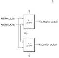
도 1에 도시된 바와 같이, 본 실시예에 따른 직병렬변환기는 내부클럭생성부(1), 데이터정렬부(2), 위상제어부(3), 선택신호생성부(4), 데이터선택부(5) 및 내부데이터생성부(6)를 포함한다.1, the serial-to-parallel converter according to the present embodiment includes an
내부클럭생성부(1)는 데이터스트로브신호(DQS) 및 반전데이터스트로브신호(DQSB)를 분주하여 제1 내부클럭(IDQS), 제2 내부클럭(QDQS), 제3 내부클럭(IDQSB) 및 제4 내부클럭(QDQSB)을 생성한다. 내부클럭생성부(1)는 주파수 분주기로 구현되고, 제1 내부클럭(IDQS), 제2 내부클럭(QDQS), 제3 내부클럭(IDQSB) 및 제4 내부클럭(QDQSB)의 주기는 데이터스트로브신호(DQS) 및 반전데이터스트로브신호(DQSB)의 주기보다 2배 크게 생성된다. 제2 내부클럭(QDQS)은 제1 내부클럭(IDQS)보다 90°만큼 위상이 늦고, 제3 내부클럭(IDQSB)은 제2 내부클럭(QDQS)보다 90°만큼 위상이 늦으며, 제4 내부클럭(QDQSB)은 제3 내부클럭(IDQSB)보다 90°만큼 위상이 늦다.The internal
데이터정렬부(2)는 제1 내부클럭(IDQS), 제2 내부클럭(QDQS), 제3 내부클럭(IDQSB) 및 제4 내부클럭(QDQSB)에 응답하여 데이터(DIN)를 정렬하여 제1 내지 제8 정렬데이터(ALIGN<1:8>)를 생성한다. 데이터정렬부(2)의 보다 구체적인 구성 및 동작은 도 2를 참고하여 후술한다.The
위상제어부(3)는 라이트커맨드(WT)가 입력되고 라이트레이턴시(WL)가 경과된 시점부터 클럭(CLK)의 정수배만큼의 주기가 경과된 시점에서 발생하는 제1 펄스를 포함하는 위상감지신호(IWT_PD)를 생성한다. 본 실시예에서, 위상감지신호(IWT_PD)의 제1 펄스는 제2 내부클럭(QDQS)의 위상을 감지하기 위해 라이트커맨드(WT)가 입력되고 라이트레이턴시(WL)가 경과된 시점부터 클럭(CLK)의 두주기 구간(2tCK) 경과한 시점에서 발생된다. 또한, 위상제어부(3)는 라이트커맨드(WT)가 입력되고 라이트레이턴시(WL)가 경과된 시점부터 클럭(CLK)의 정수배만큼의 주기가 경과된 시점에서 발생하는 제2 펄스를 포함하는 제1 데이터입력클럭(DINCLK<1>) 및 제3 펄스를 포함하는 제2 데이터입력클럭(DINCLK<2>)을 생성한다. 본 실시예에서, 제1 데이터입력클럭(DINCLK<1>)의 제2 펄스는 라이트커맨드(WT)가 입력되고 라이트레이턴시(WL)가 경과된 시점부터 클럭(CLK)의 네주기 구간(4tCK) 경과한 시점에서 발생된다. 또한, 본 실시예에서, 제2 데이터입력클럭(DINCLK<2>)의 제3 펄스는 라이트커맨드(WT)가 입력되고 라이트레이턴시(WL)가 경과된 시점부터 클럭(CLK)의 다섯주기 구간(5tCK) 경과한 시점에서 발생된다. 실시예에 따라서, 위상감지신호(IWT_PD) 및 제1 및 제2 데이터입력클럭(DINCLK<1:2>)의 펄스 발생시점 및 펄스폭은 다양하게 설정할 수 있다.The
선택신호생성부(4)는 위상감지신호(IWT_PD)에 응답하여 제1 내부클럭(IDQS), 제2 내부클럭(QDQS), 제3 내부클럭(IDQSB) 및 제4 내부클럭(QDQSB) 중 하나의 클럭을 감지하여 선택신호(SEL)를 생성한다. 본 실시예에서, 선택신호(SEL)는 위상감지신호(IWT_PD)가 발생된 시점에서 제2 내부클럭(QDQS)의 위상에 따라 논리레벨이 결정된다. 즉, 위상감지신호(IWT_PD)의 라이징 에지에서 제2 내부클럭(QDQS)이 로직하이레벨을 갖는 경우 선택신호(SEL)는 로직하이레벨을 갖고, 위상감지신호(IWT_PD)의 라이징 에지에서 제2 내부클럭(QDQS)이 로직로우레벨을 갖는 경우 선택신호(SEL)는 로직로우레벨을 갖는다. 선택신호(SEL)가 로직하이레벨로 생성되는 것은 데이터(DIN)가 입력되는 시점부터 제1 내부클럭(IDQS), 제2 내부클럭(QDQS), 제3 내부클럭(IDQSB) 및 제4 내부클럭(QDQSB)의 순서로 차례로 생성됨을 의미한다. 즉, 제1 내부클럭(IDQS), 제2 내부클럭(QDQS), 제3 내부클럭(IDQSB) 및 제4 내부클럭(QDQSB)이 정상적으로 생성될 때 선택신호(SEL)는 로직하이레벨로 생성된다. 한편, 선택신호(SEL)가 로직로우레벨로 생성되는 것은 데이터(DIN)가 입력되는 시점부터 제3 내부클럭(IDQSB), 제4 내부클럭(QDQSB)제1 내부클럭(IDQS) 및 제2 내부클럭(QDQS)의 순서로 차례로 생성됨를 의미한다. 즉, 제1 내부클럭(IDQS), 제2 내부클럭(QDQS), 제3 내부클럭(IDQSB) 및 제4 내부클럭(QDQSB)의 위상이 반전되어 생성될 때 선택신호(SEL)는 로직로우레벨로 생성된다. 실시예에 따라서, 선택신호생성부(4)는 위상감지신호(IWT_PD)에 응답하여 제1 내부클럭(IDQS), 제3 내부클럭(IDQSB) 및 제4 내부클럭(QDQSB) 중 하나를 감지하여 선택신호(SEL)를 생성하도록 설정될 수 있다.The
데이터선택부(5)는 선택신호(SEL)의 레벨에 따라 제1 내지 제8 정렬데이터(ALIGN<1:8>)를 선택적으로 제1 내지 제8 선택정렬데이터(ALIGNSEL<1:8>)로 전달한다. 본 실시예에서 데이터선택부(5)는 선택신호(SEL)가 로직하이레벨인 경우 제1 정렬데이터그룹을 제1 선택정렬데이터그룹으로 전달하고, 제2 정렬데이터그룹을 제2 선택정렬데이터그룹으로 전달한다. 제1 정렬데이터그룹은 제1 정렬데이터(ALIGN<1>), 제2 정렬데이터(ALIGN<2>), 제5 정렬데이터(ALIGN<5>) 및 제6 정렬데이터(ALIGN<6>)를 포함한다. 제2 정렬데이터그룹은 제3 정렬데이터(ALIGN<3>), 제4 정렬데이터(ALIGN<4>), 제7 정렬데이터(ALIGN<7>) 및 제8 정렬데이터(ALIGN<8>)를 포함한다. 제1 선택정렬데이터그룹은 제1 선택정렬데이터(ALIGNSEL<1>), 제2 선택정렬데이터(ALIGNSEL<2>), 제5 선택정렬데이터(ALIGNSEL<5>) 및 제6 선택정렬데이터(ALIGNSEL<6>)를 포함한다. 제2 선택정렬데이터그룹은 제3 선택정렬데이터(ALIGNSEL<3>), 제4 선택정렬데이터(ALIGNSEL<4>), 제7 선택정렬데이터(ALIGNSEL<7>) 및 제8 선택정렬데이터(ALIGNSEL<8>)를 포함한다. 한편, 본 실시예에서 데이터선택부(5)는 선택신호(SEL)가 로직로우레벨인 경우 제2 정렬데이터그룹을 제1 선택정렬데이터그룹으로 전달하고, 제1 정렬데이터그룹을 제2 선택정렬데이터그룹으로 전달한다. 데이터선택부(5)보다 구체적인 구성 및 동작은 도 3을 참고하여 후술한다.The
내부데이터생성부(6)는 제1 및 제2 데이터입력클럭(DINCLK<1:2>)에 동기하여 제1 내지 제8 선택정렬데이터(ALIGNSEL<1:8>)를 래치하여 제1 내지 제8 내부데이터(IDATA)를 래치한다. 본 실시예에서 내부데이터생성부(6)는 제1 데이터입력클럭(DINCLK<1>)에 동기하여 제1 선택정렬데이터그룹을 래치하여 제1 내부데이터그룹을 생성하고, 제2 데이터입력클럭(DINCLK<2>)에 동기하여 제2 선택정렬데이터그룹을 래치하여 제2 내부데이터그룹을 생성한다. 제1 내부데이터그룹은 제1 내부데이터(IDATA<1>), 제2 내부데이터(IDATA<2>), 제5 내부데이터(IDATA<5>) 및 제6 내부데이터(IDATA<6>)를 포함한다. 제2 내부데이터그룹은 제3 내부데이터(IDATA<3>), 제4 내부데이터(IDATA<4>), 제7 내부데이터(IDATA<7>) 및 제8 내부데이터(IDATA<8>)를 포함한다.The
도 2는 데이터정렬부(2)의 구성을 도시한 블럭도이다.FIG. 2 is a block diagram showing the configuration of the
도 2에 도시된 바와 같이, 데이터정렬부(2)는 클럭버퍼부(21) 및 정렬부(22) 로 구성된다. 클럭버퍼부(21)는 제1 내지 제4 버퍼(211~214)로 구성된다. 정렬부(22)는 제1 내지 제6 래치(221~226)로 구성된다.As shown in FIG. 2, the
제1 버퍼(211)는 제1 내부클럭(IDQS)의 라이징에지에 동기하여 데이터(DIN)를 버퍼링하여 제1 정렬데이터(ALIGN<1>)로 출력한다. 제2 버퍼(212)는 제2 내부클럭(QDQS)의 라이징에지에 동기하여 데이터(DIN)를 버퍼링하여 제2 정렬데이터(ALIGN<2>)로 출력한다. 제3 버퍼(213)는 제3 내부클럭(IDQSB)의 라이징에지에 동기하여 데이터(DIN)를 버퍼링하여 제3 정렬데이터(ALIGN<3>)로 출력한다. 제4 버퍼(214)는 제4 내부클럭(QDQSB)의 라이징에지에 동기하여 데이터(DIN)를 버퍼링하여 제4 정렬데이터(ALIGN<4>)로 출력한다. 본 실시예에서, 제1 내지 제4 버퍼(211~214)는 플립플롭으로 구현되어 입력되는 데이터를 래치하고, 버퍼링하여 출력한다.The
제1 래치(221)는 제3 내부클럭(IDQSB)의 라이징에지에 동기하여 제1 정렬데이터(ALIGN<1>)를 래치하여 출력한다. 제2 래치(222)는 제4 내부클럭(QDQSB)의 라이징에지에 동기하여 제1 래치(221)의 출력신호를 래치하여 출력한다. 제3 래치(223)는 제4 내부클럭(QDQSB)의 라이징에지에 동기하여 제2 버퍼(212)의 출력신호를 래치하여 출력한다. 제4 래치(224)는 제1 내부클럭(IDQS)의 라이징에지에 동기하여 제3 정렬데이터(ALIGN<3>)를 래치하여 출력한다. 제5 래치(225)는 제4 내부클럭(QDQSB)의 라이징에지에 동기하여 제4 래치(224)의 출력신호를 래치하여 출력한다. 제6 래치(226)는 제2 내부클럭(QDQS)의 라이징에지에 동기하여 제4 정렬데이터(ALIGN<4>)의 출력신호를 래치하여 출력한다. 본 실시예에서, 제1 내지 제6 래치(221~226)는 플립플롭으로 구현되어 입력되는 데이터를 래치하고, 버퍼링하여 출력한다.The
데이터정렬부(2)는 선택신호(SEL)가 로직하이레벨인 경우 클럭(CLK)에 동기되어 입력되는 데이터를 순차적으로 래치하여 제1 정렬데이터(ALIGN<1>), 제2 정렬데이터(ALIGN<2>), 제3 정렬데이터(ALIGN<3>) 및 제4 정렬데이터(ALIGN<1:4>)를 클럭(CLK)의 반주기구간(0.5tCK)의 구간만큼의 시간 간격으로 순차적으로 생성한다. 또한, 데이터정렬부(2)는 선택신호(SEL)가 로직하이레벨일 때 제1 정렬데이터(ALIGN<1>)를 클럭(CLK)의 1.5 주기구간(1.5tCK)만큼 지연시켜 제5 정렬데이터(ALIGN<5>)를 생성하고, 제2 정렬데이터(ALIGN<2>)를 클럭(CLK)의 1 주기구간(1tCK)만큼 지연시켜 제6 정렬데이터(ALIGN<6>)를 생성하며, 제3 정렬데이터(ALIGN<3>)를 클럭(CLK)의 1.5 주기구간(1.5tCK)만큼 지연시켜 제7 정렬데이터(ALIGN<7>)를 생성하고, 제4 정렬데이터(ALIGN<4>)를 클럭(CLK)의 1 주기구간(1tCK)만큼 지연시켜 제8 정렬데이터(ALIGN<8>)를 생성한다. 한편, 데이터정렬부(2)는 선택신호(SEL)가 로직로우레벨인 경우 클럭(CLK)에 동기되어 입력되는 데이터를 순차적으로 래치하여 제3 정렬데이터(ALIGN<3>), 제4 정렬데이터(ALIGN<1:4>)를 클럭(CLK)의 반주기구간(0.5tCK)의 구간만큼의 시간 간격으로 순차적으로 생성한다. 또한, 데이터정렬부(2)는 선택신호(SEL)가 로직로우레벨일 때 제3 정렬데이터(ALIGN<3>)를 클럭(CLK)의 1.5 주기구간(1.5tCK)만큼 지연시켜 제7 정렬데이터(ALIGN<7>)를 생성하고, 제4 정렬데이터(ALIGN<4>)를 클럭(CLK)의 1 주기구간(1tCK)만큼 지연시켜 제8 정렬데이터(ALIGN<8>)를 생성하며, 제1 정렬데이터(ALIGN<1>)를 클럭(CLK)의 1.5 주기구간(1.5tCK)만큼 지연시켜 제5 정렬데이터(ALIGN<5>)를 생성하고, 제2 정렬데이터(ALIGN<2>)를 클럭(CLK)의 1 주기구간(1tCK)만큼 지연시켜 제6 정렬데이터(ALIGN<6>)를 생성한다.When the selection signal SEL is at a logic high level, the
도 4는 데이터선택부(5)의 구성을 도시한 블럭도이다.Fig. 4 is a block diagram showing the configuration of the
도 4에 도시된 바와 같이, 데이터선택부(5)는 제1 선택부(51) 및 제2 선택부(52)로 구성된다. 제1 선택부(51)는 선택신호(SEL)가 로직하이레벨인 경우 제1 정렬데이터그룹(ALGN<1,2,5,6>)을 제1 선택정렬데이터그룹(ALGNSEL<1,2,5,6>)으로 전달한다. 제1 선택부(51)는 선택신호(SEL)가 로직로우레벨인 경우 제2 정렬데이터그룹(ALGN<3,4,7,8>)을 제1 선택정렬데이터그룹(ALGNSEL<1,2,5,6>)으로 전달한다. 제2 선택부(52)는 선택신호(SEL)가 로직하이레벨인 경우 제2 정렬데이터그룹(ALGN<3,4,7,8>)을 제2 선택정렬데이터그룹(ALGNSEL<3,4,7,8>)으로 전달한다. 제2 선택부(52)는 선택신호(SEL)가 로직로우레벨인 경우 제1 정렬데이터그룹(ALGN<1,2,5,6>)을 제2 선택정렬데이터그룹(ALGNSEL<3,4,7,8>)으로 전달한다.As shown in FIG. 4, the
이상 살펴본 직병렬변환기의 동작을 도 3 및 도 4를 참고하여 살펴보되, 데이터가 입력될 때 내부클럭들의 위상이 정상적으로 생성(선택신호(SEL)가 로직하이레벨)되는 경우와 반전되어 생성(선택신호(SEL)가 로직로우레벨)되는 경우를 나누어 살펴보면 다음과 같다. 본 실시예에서 라이트레이턴시(WL)는 2로 설정되고, tDQSS는 1tCK로 설정된 경우를 가정한다. tDQSS는 데이터스트로브신호(DQS)와 클럭(CLK) 간의 도메인 크로싱 마진에 대한 스펙을 나타낸다. 즉, tDQSS는 클럭(CLK)에 동기하여 유효한 데이터스트로브신호(DQS)가 생성되기 위해 필요한 최소구간으로 정의할 수 있다. 라이트커맨드(WT)가 입력되고, 라이트레이턴시(WL)가 경과된 시점부터 데이터(DIN)가 입력되는 시점까지의 구간은 프리앰블구간(tWPRE)으로 정의하며, 본 실시예에서 프리앰블구간(tWPRE)은 tDQSS로 설정되었지만 실시예에 따라서 tDQSS+ (정수배)*tCK의 구간으로 설정될 수 있다.3 and 4, when the phase of the internal clocks is normally generated (the selection signal SEL is at a logic high level) when data is input, the operation of the serial-to- The signal SEL is at a logic low level). In this embodiment, it is assumed that the write latency WL is set to 2 and the tDQSS is set to 1 tCK. tDQSS indicates a specification of a domain crossing margin between the data strobe signal (DQS) and the clock (CLK). That is, tDQSS can be defined as a minimum interval required for generating a valid data strobe signal DQS in synchronization with the clock CLK. A section from the time when the write command WT is input to the time when the write latency WL elapses to the time when the data DIN is input is defined as a preamble section tWPRE. In this embodiment, the preamble section tWPRE is tDQSS, but it may be set to the interval of tDQSS + (integer multiple) * tCK according to the embodiment.
도 4를 참고하여 직병렬변환기의 동작을 살펴보면 다음과 같다.The operation of the serial-to-parallel converter will be described with reference to FIG.
t11 시점에서 라이트커맨드(WT)가 입력되면 t13 시점에서 데이터(DIN)가 입력되고, 위상감지신호(IWT_PD)의 제1 펄스는 라이트레이턴시(WL)가 경과된 t12 시점부터 2tCK 구간이 경과된 t15 시점에서 발생한다. 위상감지신호(IWT_PD)의 라이징에지인 t15 시점에서 제2 내부클럭(QDQS)의 위상은 로직하이레벨이므로, 선택신호(SEL)는 로직하이레벨로 생성된다. 제1 데이터입력클럭(DINCLK<1>)의 제2 펄스는 라이트커맨드(WT)가 입력되고 라이트레이턴시(WL)가 경과된 t12시점부터 클럭(CLK)의 네주기 구간(4tCK) 경과한 t19 시점에서 발생된다. 또한, 제2 데이터입력클럭(DINCLK<2>)의 제3 펄스는 라이트커맨드(WT)가 입력되고 라이트레이턴시(WL)가 경과된 t12시점부터 클럭(CLK)의 다섯주기 구간(5tCK) 경과한 t21시점에서 발생된다.When the write command WT is input at time t11, the data DIN is input at time t13, and the first pulse of the phase detection signal IWT_PD is input to the time t15 at which 2 tCK sections have elapsed from the time t12 at which the write latency WL has elapsed. Lt; / RTI > The phase of the second internal clock signal QDQS at the time t15, which is the rising edge of the phase detection signal IWT_PD, is at a logic high level, so that the selection signal SEL is generated at a logic high level. The second pulse of the first data input clock DINCLK < 1 > is input at the timing t19 when the write command WT is inputted and after the four cycle section 4tCK of the clock CLK from the time t12 when the write latency WL has elapsed Lt; / RTI > The third pulse of the second data input clock DINCLK < 2 > is a pulse of the clock signal CLK that has elapsed from the time point t12 at which the write command WT is input and the write latency WL has elapsed to the fifth cycle interval 5tCK of the clock CLK lt; / RTI >
제1 내부클럭(IDQS), 제2 내부클럭(QDQS), 제3 내부클럭(IDQSB) 및 제4 내부클럭(QDQSB)은 tDQSS가 경과된 t13 시점부터 정상적으로 발생한다. 제1 내부클럭(IDQS)은 t13 시점에서부터 주기신호로 발생한다. 제2 내부클럭(QDQS)은 t13 시점에서 90°만큼 지연된 t14 시점에서부터 주기신호로 발생한다. 제3 내부클럭(IDQSB)은 t14 시점에서 90°만큼 지연된 t15 시점에서부터 주기신호로 발생한다. 제4 내부클럭(QDQSB)은 t15 시점에서 90°만큼 지연된 t16 시점에서부터 주기신호로 발생한다.The first internal clock IDQS, the second internal clock QDQS, the third internal clock IDQSB and the fourth internal clock QDQSB normally occur from t13 when tDQSS has elapsed. The first internal clock IDQS is generated as a periodic signal from the time t13. The second internal clock signal QDQS is generated as a periodic signal from the time t14 delayed by 90 degrees at time t13. The third internal clock IDQSB is generated as a periodic signal from a time point t15 delayed by 90 degrees at time t14. The fourth internal clock signal QDQSB is generated as a periodic signal from a time t16 delayed by 90 degrees at time t15.
데이터정렬부(2)는 클럭(CLK)에 동기되어 입력되는 데이터를 순차적으로 래치하여 제1 정렬데이터(ALIGN<1>), 제2 정렬데이터(ALIGN<2>), 제3 정렬데이터(ALIGN<3>) 및 제4 정렬데이터(ALIGN<4>)를 클럭(CLK)의 반주기구간(0.5tCK)의 구간만큼의 시간 간격으로 순차적으로 생성한다. 제1 정렬데이터(ALIGN<1>)는 t13~t17 구간동안 데이터(DIN)의 첫번째 신호를 래치하고, t17~t21 구간동안 데이터(DIN)의 다섯번째 신호를 래치한다. 제2 정렬데이터(ALIGN<2>)는 t14~t18 구간동안 데이터(DIN)의 두번째 신호를 래치하고, t18~t22 구간동안 데이터(DIN)의 여섯번째 신호를 래치한다. 제3 정렬데이터(ALIGN<3>)는 t15~t19 구간동안 데이터(DIN)의 세번째 신호를 래치하고, t19~t23 구간동안 데이터(DIN)의 일곱번째 신호를 래치한다. 제4 정렬데이터(ALIGN<4>)는 t16~t20 구간동안 데이터(DIN)의 네번째 신호를 래치하고, t20~t24 구간동안 데이터(DIN)의 여덟번째 신호를 래치한다.The
데이터정렬부(2)는 제1 정렬데이터(ALIGN<1>)를 클럭(CLK)의 1.5 주기구간(1.5tCK)만큼 지연시켜 제5 정렬데이터(ALIGN<5>)를 생성하고, 제2 정렬데이터(ALIGN<2>)를 클럭(CLK)의 1 주기구간(1tCK)만큼 지연시켜 제6 정렬데이터(ALIGN<6>)를 생성하며, 제3 정렬데이터(ALIGN<3>)를 클럭(CLK)의 1.5 주기구간(1.5tCK)만큼 지연시켜 제7 정렬데이터(ALIGN<7>)를 생성하고, 제4 정렬데이터(ALIGN<4>)를 클럭(CLK)의 1 주기구간(1tCK)만큼 지연시켜 제8 정렬데이터(ALIGN<8>)를 생성한다. 그 결과, 제5 정렬데이터(ALIGN<5>)는 t16~t20 구간동안 데이터(DIN)의 첫번째 신호를 래치하고, t20~t24 구간동안 데이터(DIN)의 다섯번째 신호를 래치한다. 제6 정렬데이터(ALIGN<6>)는 t16~t20 구간동안 데이터(DIN)의 두번째 신호를 래치하고, t20~t24 구간동안 데이터(DIN)의 여섯번째 신호를 래치한다. 제7 정렬데이터(ALIGN<7>)는 t18~t22 구간동안 데이터(DIN)의 세번째 신호를 래치하고, t22~t25 구간동안 데이터(DIN)의 일곱번째 신호를 래치한다. 제8 정렬데이터(ALIGN<8>)는 t18~t22 구간동안 데이터(DIN)의 네번째 신호를 래치하고, t22~t25 구간동안 데이터(DIN)의 여덟번째 신호를 래치한다.The
데이터선택부(5)는 로직하이레벨의 선택신호(SEL)를 입력받아, 제1 정렬데이터그룹(ALGN<1,2,5,6>)을 제1 선택정렬데이터그룹(ALGNSEL<1,2,5,6>)으로 전달하고, 제2 정렬데이터그룹(ALGN<3,4,7,8>)을 제2 선택정렬데이터그룹(ALGNSEL<3,4,7,8>)으로 전달한다. The
내부데이터생성부(6)는 제1 데이터입력클럭(DINCLK<1>)의 제2 펄스가 입력되는 t19 시점에 동기하여 제1 선택정렬데이터그룹(ALGNSEL<1,2,5,6>)을 래치하여 제1 내부데이터그룹(IDATA<1,2,5,6>)을 생성하고, 제2 데이터입력클럭(DINCLK<2>)의 제3 펄스가 입력되는 t21 시점에 동기하여 제2 선택정렬데이터그룹(ALGNSEL<3,4,7,8>)을 래치하여 제2 내부데이터그룹(DINCLK<3,4,7,8>)을 생성한다.The internal
도 5를 참고하여 직병렬변환기의 동작을 살펴보면 다음과 같다.The operation of the serial-to-parallel converter will be described with reference to FIG.
t31 시점에서 라이트커맨드(WT)가 입력되면 t33 시점에서 데이터(DIN)가 입력되고, 위상감지신호(IWT_PD)의 제1 펄스는 라이트레이턴시(WL)가 경과된 t32 시점부터 2tCK 구간이 경과된 t35 시점에서 발생한다. 위상감지신호(IWT_PD)의 라이징에지인 t35 시점에서 제2 내부클럭(QDQS)의 위상은 로직로우레벨이므로, 선택신호(SEL)는 로직로우레벨로 생성된다. 제1 데이터입력클럭(DINCLK<1>)의 제2 펄스는 라이트커맨드(WT)가 입력되고 라이트레이턴시(WL)가 경과된 t32시점부터 클럭(CLK)의 네주기 구간(4tCK) 경과한 t39 시점에서 발생된다. 또한, 제2 데이터입력클럭(DINCLK<2>)의 제3 펄스는 라이트커맨드(WT)가 입력되고 라이트레이턴시(WL)가 경과된 t32시점부터 클럭(CLK)의 다섯주기 구간(5tCK) 경과한 t41시점에서 발생된다.When the write command WT is input at time t31, the data DIN is input at time t33, and the first pulse of the phase detection signal IWT_PD is input at time t35 when the 2tCK section has elapsed from the time t32 when the write latency WL has elapsed Lt; / RTI > Since the phase of the second internal clock signal QDQS at the time t35, which is the rising edge of the phase detection signal IWT_PD, is at a logic low level, the selection signal SEL is generated at a logic low level. The second pulse of the first data input clock DINCLK < 1 > is input at the time t39 when the write command WT is input and the four cycles section 4tCK of the clock CLK has elapsed from the time t32 at which the write latency WL has elapsed Lt; / RTI > The third pulse of the second data input clock DINCLK < 2 > is a clock pulse that has passed the five cycle interval 5tCK of the clock CLK from the time point t32 when the write command WT is input and the write latency WL has elapsed lt; / RTI >
제1 내부클럭(IDQS), 제2 내부클럭(QDQS), 제3 내부클럭(IDQSB) 및 제4 내부클럭(QDQSB)은 tDQSS가 경과된 t33 시점부터 위상이 반전되어 발생한다. 제3 내부클럭(IDQSB)은 t33 시점에서부터 주기신호로 발생한다. 제4 내부클럭(QDQSB)은 t33 시점에서 90°만큼 지연된 t34 시점에서부터 주기신호로 발생한다. 제1 내부클럭(IDQS)은 t34 시점에서 90°만큼 지연된 t35 시점에서부터 주기신호로 발생한다. 제2 내부클럭(QDQS)은 t35 시점에서 90°만큼 지연된 t36 시점에서부터 주기신호로 발생한다.The first internal clock IDQS, the second internal clock QDQS, the third internal clock IDQSB and the fourth internal clock QDQSB are generated by inverting the phase from t33 when tDQSS has elapsed. The third internal clock IDQSB is generated as a periodic signal from the time t33. The fourth internal clock signal QDQSB is generated as a periodic signal from time t34 delayed by 90 degrees at time t33. The first internal clock IDQS is generated as a periodic signal from a time t35 delayed by 90 degrees at time t34. The second internal clock signal QDQS is generated as a periodic signal from the time t36 delayed by 90 degrees at time t35.
데이터정렬부(2)는 클럭(CLK)에 동기되어 입력되는 데이터를 순차적으로 래치하여 제3 정렬데이터(ALIGN<3>), 제4 정렬데이터(ALIGN<4>), 제1 정렬데이터(ALIGN<1>) 및 제2 정렬데이터(ALIGN<2>)를 클럭(CLK)의 반주기구간(0.5tCK)의 구간만큼의 시간 간격으로 순차적으로 생성한다. 제3 정렬데이터(ALIGN<3>)는 t33~t37 구간동안 데이터(DIN)의 첫번째 신호를 래치하고, t37~t41 구간동안 데이터(DIN)의 다섯번째 신호를 래치한다. 제4 정렬데이터(ALIGN<4>)는 t34~t38 구간동안 데이터(DIN)의 두번째 신호를 래치하고, t38~t42 구간동안 데이터(DIN)의 여섯번째 신호를 래치한다. 제1 정렬데이터(ALIGN<1>)는 t35~t39 구간동안 데이터(DIN)의 세번째 신호를 래치하고, t39~t43 구간동안 데이터(DIN)의 일곱번째 신호를 래치한다. 제2 정렬데이터(ALIGN<2>)는 t36~t40 구간동안 데이터(DIN)의 네번째 신호를 래치하고, t40~44 구간동안 데이터(DIN)의 여덟번째 신호를 래치한다.The
데이터정렬부(2)는 제1 정렬데이터(ALIGN<1>)를 클럭(CLK)의 1.5 주기구간(1.5tCK)만큼 지연시켜 제5 정렬데이터(ALIGN<5>)를 생성하고, 제2 정렬데이터(ALIGN<2>)를 클럭(CLK)의 1 주기구간(1tCK)만큼 지연시켜 제6 정렬데이터(ALIGN<6>)를 생성하며, 제3 정렬데이터(ALIGN<3>)를 클럭(CLK)의 1.5 주기구간(1.5tCK)만큼 지연시켜 제7 정렬데이터(ALIGN<7>)를 생성하고, 제4 정렬데이터(ALIGN<4>)를 클럭(CLK)의 1 주기구간(1tCK)만큼 지연시켜 제8 정렬데이터(ALIGN<8>)를 생성한다. 그 결과, 제7 정렬데이터(ALIGN<7>)는 t36~t40 구간동안 데이터(DIN)의 첫번째 신호를 래치하고, t40~t44 구간동안 데이터(DIN)의 다섯번째 신호를 래치한다. 제8 정렬데이터(ALIGN<8>)는 t36~t40 구간동안 데이터(DIN)의 두번째 신호를 래치하고, t40~t44 구간동안 데이터(DIN)의 여섯번째 신호를 래치한다. 제5 정렬데이터(ALIGN<5>)는 t38~t42 구간동안 데이터(DIN)의 세번째 신호를 래치하고, t42~t45 구간동안 데이터(DIN)의 일곱번째 신호를 래치한다. 제6 정렬데이터(ALIGN<6>)는 t38~t42 구간동안 데이터(DIN)의 네번째 신호를 래치하고, t42~t45 구간동안 데이터(DIN)의 여덟번째 신호를 래치한다.The
데이터선택부(5)는 로직로우레벨의 선택신호(SEL)를 입력받아, 제2 정렬데이터그룹(ALGN<3,4,7,8>)을 제1 선택정렬데이터그룹(ALGNSEL<1,2,5,6>)으로 전달하고, 제1 정렬데이터그룹(ALGN<1,2,5,6>)을 제2 선택정렬데이터그룹(ALGNSEL<3,4,7,8>)으로 전달한다. The
내부데이터생성부(6)는 제1 데이터입력클럭(DINCLK<1>)의 제2 펄스가 입력되는 t39 시점에 동기하여 제1 선택정렬데이터그룹(ALGNSEL<1,2,5,6>)을 래치하여 제1 내부데이터그룹(IDATA<1,2,5,6>)을 생성하고, 제2 데이터입력클럭(DINCLK<2>)의 제3 펄스가 입력되는 t21 시점에 동기하여 제2 선택정렬데이터그룹(ALGNSEL<3,4,7,8>)을 래치하여 제2 내부데이터그룹(DINCLK<3,4,7,8>)을 생성한다.The
이상 살펴본 바와 같이, 본 실시예에 따른 직병렬변환기는 멀티위상을 갖는 내부클럭들이 정상적으로 생성된 경우와 반전되어 비정상적으로 생성된 경우를 가정하여 데이터들을 각각 정렬시키고, 정렬된 데이터들을 위상이 반전된 데이터들을 포함하는 그룹으로 나누어 선택적으로 전달함으로써, 내부클럭의 위상이 반전된 경우에도 오류없이 데이터를 입력받아 정렬할 수 있다.
As described above, the serial-to-parallel converter according to the present embodiment aligns data on the assumption that internal clocks having multi-phases are normally generated and inverted and generated abnormally, respectively, The data can be received and arranged without error even when the phase of the internal clock is inverted.
1: 내부클럭생성부2: 데이터정렬부
3: 위상제어부4: 선택신호생성부
5: 데이터선택부6: 내부데이터생성부
21: 클럭버퍼부22: 정렬부
211~214: 제1 내지 제4 버퍼221~226: 제1 내지 제6 래치
51: 제1 선택부 52: 제2 선택부1: internal clock generating unit 2: data sorting unit
3: phase control unit 4: selection signal generation unit
5: Data selection unit 6: Internal data generation unit
21: clock buffer unit 22:
211 to 214: first to
51: first selector 52: second selector
Claims (26)
Translated fromKorean선택신호에 응답하여 제1 정렬데이터그룹 또는 제2 정렬데이터그룹을 제1 선택정렬데이터그룹으로 선택하여 전달하는 제1 선택부; 및
선택신호에 응답하여 상기 제1 정렬데이터그룹 또는 상기 제2 정렬데이터그룹을 제2 선택정렬데이터그룹으로 선택하여 전달하는 제2 선택부를 포함하는 직병렬변환기.
A selection signal generator for generating a selection signal by sensing a phase of one of the first to fourth internal clocks in response to a phase detection signal including a first pulse generated according to a write command and a write latency signal;
A first selector for selecting and delivering the first sorting data group or the second sorting data group as a first selected sorting data group in response to the selection signal; And
And a second selector for selecting and delivering the first sorting data group or the second sorting data group as a second selected sorting data group in response to the selection signal.
The serial-parallel converter of claim 1, wherein the first to fourth internal clocks are generated by dividing a data strobe signal and an inverted data strobe signal.
3. The method of claim 2, wherein the second internal clock is delayed by 90 degrees with respect to the first internal clock, the third internal clock is delayed by 90 degrees with respect to the second internal clock, Is phase shifted by 90 degrees with respect to the third internal clock.
제1 내부클럭에 동기하여 데이터가 래치되어 생성된 제1 정렬데이터, 제2 내부클럭에 동기하여 상기 데이터가 래치되어 생성된 제2 정렬데이터, 제3 내부클럭에 동기하여 상기 데이터가 래치되어 생성된 제4 정렬데이터, 상기 제3 및 제4 내부클럭에 동기하여 상기 제1 정렬데이터가 래치되어 생성된 제5 정렬데이터, 상기 제4 내부클럭에 동기하여 상기 제2 정렬데이터가 래치되어 생성된 제6 정렬데이터, 상기 제1 및 제4 내부클럭에 동기하여 상기 제3 정렬데이터가 래치되어 생성된 제7 정렬데이터 및 상기 제2 내부클럭에 동기하여 상기 제4 정렬데이터가 래치되어 생성된 제8 정렬데이터 중에서, 상기 제1 정렬데이터그룹은 상기 제1, 제2, 제5 및 제6 정렬데이터를 포함하고, 상기 제2 정렬데이터그룹은 상기 제3, 제4, 제7 및 제8 정렬데이터를 포함하는 직병렬변환기.
The method according to claim 1,
The first alignment data generated by latching the data in synchronization with the first internal clock, the second alignment data generated by latching the data in synchronization with the second internal clock, the data is latched and generated in synchronization with the third internal clock Fourth alignment data generated by latching the first alignment data in synchronization with the third and fourth internal clocks, and second alignment data generated by latching and generating the second alignment data in synchronization with the fourth internal clock Sixth alignment data, seventh alignment data generated by latching the third alignment data in synchronization with the first and fourth internal clocks, and seventh alignment data generated by latching the fourth alignment data in synchronization with the second internal clock The first sorting data group includes the first, second, fifth, and sixth sorting data, and the second sorting data group includes the third, fourth, seventh, and eighth sorting data Occupational duties containing data Column converter.
The method of claim 1, wherein the selection signal has a first level when the first internal clock, the second internal clock, the third internal clock, and the fourth internal clock are generated in the order of data input And a second level when the third internal clock, the fourth internal clock, the first internal clock, and the third internal clock are generated in the order of the input of the data.
6. The serial-to-parallel converter according to claim 5, wherein when the selection signal has the first level, the first selector selects and delivers the first sorting data group as the first selected sorting data group.
7. The serial-parallel converter according to claim 6, wherein when the selection signal has the first level, the second selector selects and delivers the second sorting data group as the second selection sorting data group.
8. The serial-to-parallel converter according to claim 7, wherein when the selection signal has the second level, the first selector selects and delivers the second sorting data group as the first selected sorting data group.
9. The serial-to-parallel converter according to claim 8, wherein, when the selection signal has the second level, the second selector selects and delivers the first sorting data group as the second selection sorting data group.
The serial-to-parallel converter according to claim 1, wherein the first pulse of the phase detection signal is generated after the write command is input and a period corresponding to an integer multiple of a clock has elapsed after a write latency period has elapsed.
The method of claim 1, further comprising: latching the first selected sorting data group in response to a first data input clock including a second pulse generated in accordance with the write command and the write latency signal to generate a first internal data group And an internal data generating unit.
12. The data latch circuit according to claim 11, wherein the internal data generator latches the second selected sorting data group in response to a second data input clock including a third pulse generated in accordance with the write command and the write latency signal, A serial-to-parallel converter for generating data groups.
The serial-parallel converter according to claim 12, wherein the second pulse of the first data input clock is generated after the write command is input and a period corresponding to an integer multiple of the clock has elapsed after the write latency period has elapsed.
14. The serial-to-parallel converter according to claim 13, wherein the third pulse of the second data input clock is generated after the second pulse of the first data input clock is generated after an interval of an integer multiple of the clock has elapsed.
상기 위상감지신호에 응답하여 제1 내지 제4 내부클럭 중 하나의 클럭의 위상을 감지하여 생성된 선택신호에 응답하여 제1 정렬데이터그룹 또는 제2 정렬데이터그룹을 제1 선택정렬데이터그룹으로 선택하여 전달하고, 상기 선택신호에 응답하여 상기 제1 정렬데이터그룹 또는 상기 제2 정렬데이터그룹을 제2 선택정렬데이터그룹으로 선택하여 전달하는 데이터선택부; 및
상기 제1 데이터입력클럭에 응답하여 상기 제1 선택정렬데이터그룹을 래치하여 제1 내부데이터그룹을 생성하고, 상기 제2 데이터입력클럭에 응답하여 상기 제2 선택정렬데이터그룹을 래치하여 제2 내부데이터그룹을 생성하는 내부데이터생성부를 포함하는 직병렬변환기.
A phase control unit generating a second data input clock including a phase detection signal including a first pulse generated according to a write command and a write latency signal, a first data input clock including a second pulse, and a third pulse;
In response to the selection signal generated by sensing the phase of one of the first to fourth internal clocks in response to the phase detection signal, selects the first sorting data group or the second sorting data group as the first selected sorting data group A data selector for selecting the first sorting data group or the second sorting data group as a second selected sorting data group in response to the selection signal; And
Latching the first selected sorting data group in response to the first data input clock to generate a first internal data group and latching the second selected sorting data group in response to the second data input clock, And an internal data generator for generating a data group.
16. The serial-to-parallel converter according to claim 15, wherein the first pulse of the phase detection signal is generated after the write command is input and a period corresponding to an integer multiple of the clock has elapsed after the write latency period has elapsed.
16. The serial-parallel converter of claim 15, wherein the second pulse of the first data input clock is generated after the write command is input and a period of an integer multiple of the clock has elapsed after the write latency period has elapsed.
18. The serial-to-parallel converter according to claim 17, wherein the third pulse of the second data input clock is generated after an interval of an integer multiple of the clock has elapsed after the second pulse of the first data input clock has been generated.
16. The serial-to-parallel converter according to claim 15, wherein the first to fourth internal clocks are generated by dividing a data strobe signal and an inverted data strobe signal.
The method of claim 19, wherein the second internal clock is delayed by 90 degrees with respect to the first internal clock, the third internal clock is delayed by 90 degrees with respect to the second internal clock, Is phase shifted by 90 degrees with respect to the third internal clock.
제1 내부클럭에 동기하여 데이터가 래치되어 생성된 제1 정렬데이터, 제2 내부클럭에 동기하여 상기 데이터가 래치되어 생성된 제2 정렬데이터, 제3 내부클럭에 동기하여 상기 데이터가 래치되어 생성된 제4 정렬데이터, 상기 제3 및 제4 내부클럭에 동기하여 상기 제1 정렬데이터가 래치되어 생성된 제5 정렬데이터, 상기 제4 내부클럭에 동기하여 상기 제2 정렬데이터가 래치되어 생성된 제6 정렬데이터, 상기 제1 및 제4 내부클럭에 동기하여 상기 제3 정렬데이터가 래치되어 생성된 제7 정렬데이터 및 상기 제2 내부클럭에 동기하여 상기 제4 정렬데이터가 래치되어 생성된 제8 정렬데이터 중에서, 상기 제1 정렬데이터그룹은 상기 제1, 제2, 제5 및 제6 정렬데이터를 포함하고, 상기 제2 정렬데이터그룹은 상기 제3, 제4, 제7 및 제8 정렬데이터를 포함하는 직병렬변환기.
16. The method of claim 15,
The first alignment data generated by latching the data in synchronization with the first internal clock, the second alignment data generated by latching the data in synchronization with the second internal clock, the data is latched and generated in synchronization with the third internal clock Fourth alignment data generated by latching the first alignment data in synchronization with the third and fourth internal clocks, and second alignment data generated by latching and generating the second alignment data in synchronization with the fourth internal clock Sixth alignment data, seventh alignment data generated by latching the third alignment data in synchronization with the first and fourth internal clocks, and seventh alignment data generated by latching the fourth alignment data in synchronization with the second internal clock The first sorting data group includes the first, second, fifth, and sixth sorting data, and the second sorting data group includes the third, fourth, seventh, and eighth sorting data Occupational duties containing data Column converter.
16. The method of claim 15, wherein the select signal has a first level when the first internal clock, the second internal clock, the third internal clock, and the fourth internal clock are generated in the order of data input And a second level when the third internal clock, the fourth internal clock, the first internal clock, and the third internal clock are generated in the order of the input of the data.
23. The deserializer according to claim 22, wherein the data selector selects and delivers the first sorting data group as the first selected sorting data group when the selection signal has the first level.
24. The serial-to-parallel converter according to claim 23, wherein the data selector selects and delivers the second sorting data group as the second selected sorting data group when the selection signal has the first level.
25. The deserializer of claim 24, wherein the data selector selects and delivers the second sorting data group as the first selected sorting data group when the selection signal has the second level.
Priority Applications (5)
| Application Number | Priority Date | Filing Date | Title |
|---|---|---|---|
| KR1020120137369AKR101886671B1 (en) | 2012-11-29 | 2012-11-29 | Deserializer |
| US13/846,906US8823426B2 (en) | 2012-10-24 | 2013-03-18 | Deserializers |
| CN201310302936.5ACN103780265B (en) | 2012-10-24 | 2013-07-18 | Deserializer and method of deserialization |
| US14/446,574US8928370B2 (en) | 2012-10-24 | 2014-07-30 | Deserializers |
| US14/446,603US8928371B2 (en) | 2012-10-24 | 2014-07-30 | Deserializers |
Applications Claiming Priority (1)
| Application Number | Priority Date | Filing Date | Title |
|---|---|---|---|
| KR1020120137369AKR101886671B1 (en) | 2012-11-29 | 2012-11-29 | Deserializer |
Publications (2)
| Publication Number | Publication Date |
|---|---|
| KR20140069727Atrue KR20140069727A (en) | 2014-06-10 |
| KR101886671B1 KR101886671B1 (en) | 2018-08-09 |
Family
ID=51124758
Family Applications (1)
| Application Number | Title | Priority Date | Filing Date |
|---|---|---|---|
| KR1020120137369AExpired - Fee RelatedKR101886671B1 (en) | 2012-10-24 | 2012-11-29 | Deserializer |
Country Status (1)
| Country | Link |
|---|---|
| KR (1) | KR101886671B1 (en) |
Citations (2)
| Publication number | Priority date | Publication date | Assignee | Title |
|---|---|---|---|---|
| KR950025539A (en)* | 1994-02-04 | 1995-09-18 | 김광호 | Serial and parallel conversion interface circuit |
| KR20120110431A (en)* | 2011-03-29 | 2012-10-10 | 에스케이하이닉스 주식회사 | A semiconductor memory apparatus |
- 2012
- 2012-11-29KRKR1020120137369Apatent/KR101886671B1/ennot_activeExpired - Fee Related
Patent Citations (2)
| Publication number | Priority date | Publication date | Assignee | Title |
|---|---|---|---|---|
| KR950025539A (en)* | 1994-02-04 | 1995-09-18 | 김광호 | Serial and parallel conversion interface circuit |
| KR20120110431A (en)* | 2011-03-29 | 2012-10-10 | 에스케이하이닉스 주식회사 | A semiconductor memory apparatus |
Also Published As
| Publication number | Publication date |
|---|---|
| KR101886671B1 (en) | 2018-08-09 |
Similar Documents
| Publication | Publication Date | Title |
|---|---|---|
| KR102143654B1 (en) | Semiconductor memory device | |
| US7975162B2 (en) | Apparatus for aligning input data in semiconductor memory device | |
| KR100639616B1 (en) | Delay-Locked Loops and Locking Methods in Semiconductor Memory Devices | |
| KR102517463B1 (en) | Semiconductor device | |
| US10725950B2 (en) | Peripheral interface circuit for serial memory | |
| US7499370B2 (en) | Synchronous semiconductor memory device | |
| KR101009335B1 (en) | Semiconductor memory device and driving method thereof | |
| KR102167598B1 (en) | Semiconductor device | |
| KR20190020390A (en) | Semiconductor device | |
| US8928371B2 (en) | Deserializers | |
| KR20150080060A (en) | Receiver circuit for correcting skew, semiconductor apparatus and system including the same | |
| US7450442B2 (en) | Semiconductor memory device with increased domain crossing margin | |
| KR101905894B1 (en) | Semiconductor chip and semiconductor system | |
| JP2009043342A (en) | Semiconductor memory device | |
| KR101246986B1 (en) | Memory device including a memory block having a fixed latency data output | |
| KR20090071893A (en) | Data input circuit of semiconductor memory device and control method thereof | |
| KR20150005366A (en) | Semiconductor device and semiconductor system | |
| JP5005928B2 (en) | Interface circuit and storage control device including the interface circuit | |
| KR100884589B1 (en) | Multi phase clock generator and multi phase clock generation method | |
| US7561490B2 (en) | Semiconductor memory device and method for driving the same | |
| KR20140052417A (en) | Deserializer | |
| US20150035575A1 (en) | Data output circuits | |
| KR101886671B1 (en) | Deserializer | |
| US9058859B2 (en) | Data output circuit | |
| KR101914297B1 (en) | Deserializer |
Legal Events
| Date | Code | Title | Description |
|---|---|---|---|
| PA0109 | Patent application | St.27 status event code:A-0-1-A10-A12-nap-PA0109 | |
| PN2301 | Change of applicant | St.27 status event code:A-3-3-R10-R13-asn-PN2301 St.27 status event code:A-3-3-R10-R11-asn-PN2301 | |
| PG1501 | Laying open of application | St.27 status event code:A-1-1-Q10-Q12-nap-PG1501 | |
| PN2301 | Change of applicant | St.27 status event code:A-3-3-R10-R13-asn-PN2301 St.27 status event code:A-3-3-R10-R11-asn-PN2301 | |
| P22-X000 | Classification modified | St.27 status event code:A-2-2-P10-P22-nap-X000 | |
| A201 | Request for examination | ||
| PA0201 | Request for examination | St.27 status event code:A-1-2-D10-D11-exm-PA0201 | |
| P11-X000 | Amendment of application requested | St.27 status event code:A-2-2-P10-P11-nap-X000 | |
| P13-X000 | Application amended | St.27 status event code:A-2-2-P10-P13-nap-X000 | |
| E902 | Notification of reason for refusal | ||
| PE0902 | Notice of grounds for rejection | St.27 status event code:A-1-2-D10-D21-exm-PE0902 | |
| P11-X000 | Amendment of application requested | St.27 status event code:A-2-2-P10-P11-nap-X000 | |
| P13-X000 | Application amended | St.27 status event code:A-2-2-P10-P13-nap-X000 | |
| E701 | Decision to grant or registration of patent right | ||
| PE0701 | Decision of registration | St.27 status event code:A-1-2-D10-D22-exm-PE0701 | |
| PR0701 | Registration of establishment | St.27 status event code:A-2-4-F10-F11-exm-PR0701 | |
| PR1002 | Payment of registration fee | St.27 status event code:A-2-2-U10-U11-oth-PR1002 Fee payment year number:1 | |
| PG1601 | Publication of registration | St.27 status event code:A-4-4-Q10-Q13-nap-PG1601 | |
| PR1001 | Payment of annual fee | St.27 status event code:A-4-4-U10-U11-oth-PR1001 Fee payment year number:4 | |
| PR1001 | Payment of annual fee | St.27 status event code:A-4-4-U10-U11-oth-PR1001 Fee payment year number:5 | |
| PC1903 | Unpaid annual fee | St.27 status event code:A-4-4-U10-U13-oth-PC1903 Not in force date:20230803 Payment event data comment text:Termination Category : DEFAULT_OF_REGISTRATION_FEE | |
| PC1903 | Unpaid annual fee | St.27 status event code:N-4-6-H10-H13-oth-PC1903 Ip right cessation event data comment text:Termination Category : DEFAULT_OF_REGISTRATION_FEE Not in force date:20230803 |