KR20140068627A - Resistive random access memory devices having variable resistance layers and methods for fabricating the same - Google Patents
Resistive random access memory devices having variable resistance layers and methods for fabricating the sameDownload PDFInfo
- Publication number
- KR20140068627A KR20140068627AKR1020120136333AKR20120136333AKR20140068627AKR 20140068627 AKR20140068627 AKR 20140068627AKR 1020120136333 AKR1020120136333 AKR 1020120136333AKR 20120136333 AKR20120136333 AKR 20120136333AKR 20140068627 AKR20140068627 AKR 20140068627A
- Authority
- KR
- South Korea
- Prior art keywords
- film
- channel
- gate
- vertical
- insulating film
- Prior art date
- Legal status (The legal status is an assumption and is not a legal conclusion. Google has not performed a legal analysis and makes no representation as to the accuracy of the status listed.)
- Withdrawn
Links
Images


Classifications
- H—ELECTRICITY
- H10—SEMICONDUCTOR DEVICES; ELECTRIC SOLID-STATE DEVICES NOT OTHERWISE PROVIDED FOR
- H10N—ELECTRIC SOLID-STATE DEVICES NOT OTHERWISE PROVIDED FOR
- H10N70/00—Solid-state devices having no potential barriers, and specially adapted for rectifying, amplifying, oscillating or switching
- H10N70/20—Multistable switching devices, e.g. memristors
- H10N70/24—Multistable switching devices, e.g. memristors based on migration or redistribution of ionic species, e.g. anions, vacancies
- H—ELECTRICITY
- H10—SEMICONDUCTOR DEVICES; ELECTRIC SOLID-STATE DEVICES NOT OTHERWISE PROVIDED FOR
- H10B—ELECTRONIC MEMORY DEVICES
- H10B63/00—Resistance change memory devices, e.g. resistive RAM [ReRAM] devices
- H10B63/30—Resistance change memory devices, e.g. resistive RAM [ReRAM] devices comprising selection components having three or more electrodes, e.g. transistors
- H10B63/34—Resistance change memory devices, e.g. resistive RAM [ReRAM] devices comprising selection components having three or more electrodes, e.g. transistors of the vertical channel field-effect transistor type
- H—ELECTRICITY
- H10—SEMICONDUCTOR DEVICES; ELECTRIC SOLID-STATE DEVICES NOT OTHERWISE PROVIDED FOR
- H10B—ELECTRONIC MEMORY DEVICES
- H10B63/00—Resistance change memory devices, e.g. resistive RAM [ReRAM] devices
- H10B63/80—Arrangements comprising multiple bistable or multi-stable switching components of the same type on a plane parallel to the substrate, e.g. cross-point arrays
- H10B63/84—Arrangements comprising multiple bistable or multi-stable switching components of the same type on a plane parallel to the substrate, e.g. cross-point arrays arranged in a direction perpendicular to the substrate, e.g. 3D cell arrays
- H—ELECTRICITY
- H10—SEMICONDUCTOR DEVICES; ELECTRIC SOLID-STATE DEVICES NOT OTHERWISE PROVIDED FOR
- H10D—INORGANIC ELECTRIC SEMICONDUCTOR DEVICES
- H10D84/00—Integrated devices formed in or on semiconductor substrates that comprise only semiconducting layers, e.g. on Si wafers or on GaAs-on-Si wafers
- H10D84/01—Manufacture or treatment
- H10D84/0123—Integrating together multiple components covered by H10D12/00 or H10D30/00, e.g. integrating multiple IGBTs
- H10D84/0126—Integrating together multiple components covered by H10D12/00 or H10D30/00, e.g. integrating multiple IGBTs the components including insulated gates, e.g. IGFETs
- H10D84/016—Integrating together multiple components covered by H10D12/00 or H10D30/00, e.g. integrating multiple IGBTs the components including insulated gates, e.g. IGFETs the components including vertical IGFETs
- H—ELECTRICITY
- H10—SEMICONDUCTOR DEVICES; ELECTRIC SOLID-STATE DEVICES NOT OTHERWISE PROVIDED FOR
- H10N—ELECTRIC SOLID-STATE DEVICES NOT OTHERWISE PROVIDED FOR
- H10N70/00—Solid-state devices having no potential barriers, and specially adapted for rectifying, amplifying, oscillating or switching
- H10N70/801—Constructional details of multistable switching devices
- H10N70/821—Device geometry
- H10N70/826—Device geometry adapted for essentially vertical current flow, e.g. sandwich or pillar type devices
- H10N70/8265—Device geometry adapted for essentially vertical current flow, e.g. sandwich or pillar type devices on sidewalls of dielectric structures, e.g. mesa-shaped or cup-shaped devices
- H—ELECTRICITY
- H10—SEMICONDUCTOR DEVICES; ELECTRIC SOLID-STATE DEVICES NOT OTHERWISE PROVIDED FOR
- H10N—ELECTRIC SOLID-STATE DEVICES NOT OTHERWISE PROVIDED FOR
- H10N70/00—Solid-state devices having no potential barriers, and specially adapted for rectifying, amplifying, oscillating or switching
- H10N70/801—Constructional details of multistable switching devices
- H10N70/881—Switching materials
- H10N70/883—Oxides or nitrides
- H10N70/8833—Binary metal oxides, e.g. TaOx
Landscapes
- Semiconductor Memories (AREA)
Abstract
Translated fromKoreanDescription
Translated fromKorean본 발명은 반도체에 관한 것으로, 보다 구체적으로는 저항 메모리 소자 및 그 제조방법에 관한 것이다.BACKGROUND OF THE
가변저항체로 구성된 박막에 전압이 인가되면 그 전압의 방향에 따라 박막의 저항이 현저히 변하는 현상이 발견되었고 이러한 현상이 메모리 소자에 응용되었다. 이처럼 인가된 전압의 극성에 의존하여 저항값이 달라지는 가변저항막을 이용하는 것이 불휘발 특성을 갖는 저항 메모리 소자이다.When a voltage is applied to a thin film composed of a variable resistor, the resistance of the thin film is remarkably changed according to the direction of the voltage. This phenomenon is applied to the memory device. The use of a variable resistance film whose resistance value varies depending on the polarity of the applied voltage is a resistive memory element having a nonvolatile characteristic.
본 발명의 목적은 개선된 전기적 특성을 갖는 저항 메모리 소자 및 그 제조방법을 제공함에 있다.It is an object of the present invention to provide a resistance memory device having improved electrical characteristics and a method of manufacturing the same.
상기 목적을 달성하기 위한 본 발명에 따른 저항 메모리 소자 및 그 제조방법은 게이트들을 수직방향으로 적층하고, 게이트들을 수평방향으로 리세스시키고 가변저항막을 리세스된 게이트들을 향해 신장된 돌출부를 형성하는 것을 특징으로 한다.According to an aspect of the present invention, there is provided a method of fabricating a resistive memory device including the steps of stacking gates in a vertical direction, recessing gates in a horizontal direction, and forming a protruding portion of the variable resistive film toward the recessed gates .
본 발명은 채널을 리세스된 게이트들을 따라 수직방향 및 수평방향으로 반복되게 연장되게 형성하고, 가변저항막의 돌출부가 채널의 수직방향으로 연장된 부분을 가로지르는 형태로 형성하는 것을 다른 특징으로 한다.The present invention is characterized in that the channel is formed so as to repeatedly extend in the vertical direction and the horizontal direction along the recessed gates, and the projecting portion of the variable resistance film is formed to cross the portion extending in the vertical direction of the channel.
본 발명은 가변저항막의 돌출부에 필라멘트가 생성되게 하여 채널을 따라 흐르는 전류를 필라멘트를 경유하게 하므로써 전류를 수직하게 흐르게 하는 것을 특징으로 한다. The present invention is characterized in that a filament is generated in a protruding portion of a variable resistance film so that a current flowing along a channel is passed through a filament to flow a current perpendicularly.
상기 특징을 구현할 수 있는 본 발명의 실시예에 따른 저항 메모리 소자는: 기판 상에 절연막들과 게이트들이 수직방향으로 적층된 게이트 스택; 상기 게이트 스택을 상기 수직방향으로 관통하여 상기 기판과 전기적으로 연결되는 채널; 상기 채널과 상기 게이트들 사이에 배치된 게이트 절연막; 그리고 상기 채널의 연장방향을 따라 배치된 가변저항막을 포함할 수 있다. 상기 게이트 스택은 상기 게이트가 수평방향으로 리세스되어 형성된 벽감을 포함할 수 있다. 상기 가변저항막은 상기 벽감을 향해 상기 수평방향으로 신장되고 상기 게이트들 중 적어도 어느 하나와 상기 수평방향으로 오버랩될 수 있다.A resistive memory device according to an embodiment of the present invention capable of realizing the above features includes: a gate stack in which insulating films and gates are stacked in a vertical direction on a substrate; A channel penetrating the gate stack in the vertical direction and electrically connected to the substrate; A gate insulating film disposed between the channel and the gates; And a variable resistance film disposed along the extending direction of the channel. The gate stack may include a niche formed by recessing the gate in a horizontal direction. The variable resistive film may extend in the horizontal direction toward the niche and overlap with at least one of the gates in the horizontal direction.
본 실시예의 소자에 있어서, 상기 가변저항막은: 상기 채널을 따라 상기 수직방향으로 연장된 수직막과; 상기 수직막으로부터 상기 수평방향으로 신장된 돌출부를 포함할 수 있다.In the element of the present embodiment, the variable resistance film includes: a vertical film extending in the vertical direction along the channel; And a protrusion extending in the horizontal direction from the vertical film.
본 실시예의 소자에 있어서, 상기 채널은: 상기 절연막을 따라 상기 수직방향으로 연장되어 상기 돌출부와 상기 수직방향으로 오버랩되는 제1 채널부와; 상기 벽감 내에서 상기 게이트를 따라 상기 수직방향으로 연장되어 상기 게이트와 상기 수평방향으로 오버랩되는 제2 채널부와; 그리고 상기 벽감 내에서 상기 수평방향으로 연장되어 상기 제1 채널부와 상기 제2 채널부를 이어주는 제3 채널부를 포함할 수 있다. 상기 채널은 상기 게이트 스택 내에서 상기 수직방향으로 연속적으로 연장될 수 있다.In the device of this embodiment, the channel may include: a first channel portion extending in the vertical direction along the insulating film and overlapping with the protrusion in the vertical direction; A second channel portion extending in the vertical direction along the gate in the niche and overlapped with the gate in the horizontal direction; And a third channel portion extending in the horizontal direction within the niche and connecting the first channel portion and the second channel portion. The channel may extend continuously in the vertical direction within the gate stack.
본 실시예의 소자에 있어서, 상기 가변저항막의 수직막은 상기 제1 채널부를 따라 상기 수직방향으로 연장될 수 있다. 상기 가변저항막의 돌출부는 상기 벽감 내부로 삽입되고 상기 제1 채널부의 두께보다 큰 길이를 가질 수 있다.In the device of this embodiment, the vertical film of the variable resistance film may extend in the vertical direction along the first channel portion. The projecting portion of the variable resistive film may be inserted into the inside of the niche and have a length larger than the thickness of the first channel portion.
본 실시예의 소자에 있어서, 상기 가변저항막의 수직막은 상기 제1 채널부를 따라 상기 수직방향으로 연장될 수 있다. 상기 가변저항막의 돌출부는 상기 벽감 내부로 삽입되지 아니하고 상기 제1 채널부의 두께와 동일하거나 작은 길이를 가질 수 있다.In the device of this embodiment, the vertical film of the variable resistance film may extend in the vertical direction along the first channel portion. The projecting portion of the variable resistance film may have a length equal to or less than the thickness of the first channel portion without being inserted into the interior of the niche.
본 실시예의 소자에 있어서, 상기 제2 채널부는 상기 제1 채널부 및 상기 제3 채널부에 비해 작은 두께를 가질 수 있다.In the device of the present embodiment, the second channel portion may have a thickness smaller than that of the first channel portion and the third channel portion.
본 실시예의 소자에 있어서, 상기 게이트의 길이는 상기 제2 채널부의 길이보다 클 수 있다.In the device of this embodiment, the length of the gate may be greater than the length of the second channel portion.
본 실시예의 소자에 있어서, 상기 게이트 절연막은: 상기 절연막의 측면과 상기 제1 채널부 사이에 배치된 제1 게이트 절연막과; 상기 벽감 내에서 상기 게이트와 상기 제2 채널부 사이에 배치된 제2 게이트 절연막; 그리고 상기 벽감 내에서 상기 수평방향으로 연장되어 상기 제1 게이트 절연막과 상기 제2 게이트 절연막을 이어주는 제3 게이트 절연막을 포함하여 상기 게이트 스택 내에서 상기 수직방향으로 연속적인 형태를 가질 수 있다.In the device of this embodiment, the gate insulating film may include: a first gate insulating film disposed between a side surface of the insulating film and the first channel portion; A second gate insulating film disposed between the gate and the second channel portion in the niches; And a third gate insulating film extending in the horizontal direction within the niches to connect the first gate insulating film and the second gate insulating film, and may have a continuous shape in the vertical direction in the gate stack.
본 실시예의 소자에 있어서, 상기 게이트 절연막은 상기 게이트와 상기 제2 채널부에 삽입된 아일랜드 형태를 가질 수 있다.In the device of this embodiment, the gate insulating film may have an island shape inserted into the gate and the second channel portion.
본 실시예의 소자에 있어서, 상기 제2 게이트 절연막은 상기 제1 게이트 절연막 및 상기 제3 게이트 절연막에 비해 큰 두께를 가질 수 있다.In the device of this embodiment, the second gate insulating film may have a larger thickness than the first gate insulating film and the third gate insulating film.
본 실시예의 소자에 있어서, 상기 가변저항막은 상기 벽감 내부로 삽입된 복수개의 돌출부들을 포함할 수 있다. 상기 돌출부들은 상기 채널의 연장방향을 따라 상기 수직방향으로 불연속적으로 배열될 수 있다.In the element of the present embodiment, the variable resistance film may include a plurality of protrusions inserted into the inside of the niche. The protrusions may be discontinuously arranged in the vertical direction along the extending direction of the channel.
상기 특징을 구현할 수 있는 본 발명의 실시예에 따른 저항 메모리 소자의 제조방법은: 기판 상에 절연막들과 희생막들을 적층하고; 상기 절연막들과 희생막들을 수직 관통하는 수직홀을 형성하고; 상기 희생막들을 수평하게 리세스시켜 상기 수직홀 내에 벽감을 형성하고; 상기 벽감의 내면을 따라 굴곡 연장되는 채널을 형성하고; 상기 벽감을 향해 신장되어 상기 채널을 수평하게 가로지르는 가변저항막을 형성하고; 그리고 상기 희생막들을 게이트들로 대체하는 것을 포함할 수 있다. 상기 가변저항막은 상기 게이트들 중 적어도 어느 하나와 수평하게 오버랩될 수 있다.A method of fabricating a resistive memory device according to an embodiment of the present invention capable of realizing the above features comprises: laminating insulating films and sacrificial films on a substrate; A vertical hole penetrating through the insulating films and the sacrificial films vertically; Horizontally recessing the sacrificial films to form a niche within the vertical holes; Forming a channel that bends along the inner surface of the niche; Forming a variable resistive film extending horizontally across the channel extending toward the niche; And replacing the sacrificial films with gates. The variable resistance film may overlap horizontally with at least one of the gates.
본 실시예의 방법에 있어서, 상기 가변저항막을 형성하는 것은: 상기 채널이 형성된 수직홀을 전이금속산화막으로 채워, 상기 수직홀을 따라 수직 연장된 수직막과; 상기 수직막으로부터 연장되어 상기 벽감을 향해 돌출되는 돌출부를 형성하는 것을 포함할 수 있다. 상기 가변저항막은, 상기 수직홀 내에서 상기 게이트들의 적층 방향을 따라 수직 연장된 하단은 닫히고 상단은 열린 컵 형태와 상기 수직홀을 완전히 채우는 기둥 형태 중 어느 하나일 수 있다.In the method of this embodiment, forming the variable resistance film may include: forming a vertical hole in which the vertical hole in which the channel is formed is filled with a transition metal oxide film and extends vertically along the vertical hole; And forming protrusions extending from the vertical film and protruding toward the niche. The variable resistance film may be any one of a vertically extending lower end closed along the stacking direction of the gates in the vertical hole, and an upper end opened form and a column form completely filling the vertical hole.
본 실시예의 방법에 있어서, 상기 가변저항막을 형성하는 것은: 상기 채널이 형성된 수직홀을 전이금속산화막으로 채워, 상기 수직홀을 따라 수직 연장된 수직막과; 상기 수직막으로부터 연장되어 상기 벽감을 향해 돌출되는 돌출부를 형성하고; 그리고 상기 수직막을 선택적으로 제거하는 것을 포함할 수 있다. 상기 가변저항막은 상기 수직홀 내에서 상기 게이트들의 적층 방향을 따라 불연속적으로 배열된 복수개의 돌출부들일 수 있다.In the method of this embodiment, forming the variable resistance film may include: forming a vertical hole in which the vertical hole in which the channel is formed is filled with a transition metal oxide film and extends vertically along the vertical hole; A protrusion extending from the vertical film and protruding toward the niche; And selectively removing the vertical film. The variable resistive film may be a plurality of protrusions arranged discontinuously along the stacking direction of the gates in the vertical holes.
본 실시예의 방법에 있어서, 상기 희생막을 게이트들로 대체하는 것은: 상기 희생막들과 상기 절연막들을 패터닝하여 상기 기판을 노출시키는 트렌치를 형성하고; 상기 트렌치를 통해 노출된 상기 희생막들을 선택적으로 제거하여 상기 절연막들 사이에 스페이스들을 형성하고; 그리고 상기 스페이스들을 도전막으로 채워 상기 게이트들을 형성하는 것을 포함할 수 있다.In the method of this embodiment, replacing the sacrificial film with gates: patterning the sacrificial films and the insulating films to form a trench exposing the substrate; Selectively removing the sacrificial layers exposed through the trench to form spaces between the insulating films; And filling the spaces with a conductive film to form the gates.
본 실시예의 방법에 있어서, 상기 채널과 상기 게이트들 사이에 게이트 절연막을 형성하는 것을 더 포함할 수 있다.In the method of this embodiment, it may further comprise forming a gate insulating film between the channel and the gates.
본 실시예의 방법에 있어서, 상기 게이트 절연막을 형성하는 것은: 상기 채널을 형성하기 이전에, 상기 수직홀의 내측벽과 상기 기판을 덮는 증착막을 형성한 후 상기 기판을 덮는 증착막을 선택적으로 제거하여 상기 기판을 노출시키는 것을 포함할 수 있다.Forming a gate insulating film on the substrate; forming a gate insulating film on the gate insulating film; forming a deposition film covering the inner wall of the vertical hole and the substrate before forming the channel; Lt; / RTI >
본 실시예의 방법에 있어서, 상기 게이트 절연막을 형성하는 것은: 상기 스페이스들을 형성한 이후에, 상기 스페이스들을 통해 노출된 상기 채널의 측면을 열산화시키는 것을 포함할 수 있다.In the method of this embodiment, forming the gate insulator film may include: after forming the spaces, thermally oxidizing the side of the channel exposed through the spaces.
본 실시예의 방법에 있어서, 상기 게이트 절연막을 형성하는 것은: 상기 채널을 형성하기 이전에, 상기 수직홀의 내측벽과 상기 기판을 덮는 증착막을 형성한 후 상기 기판을 덮는 증착막을 선택적으로 제거하여 상기 기판을 노출시키고, 상기 스페이스들을 형성한 이후에 상기 스페이스들을 통해 노출된 상기 게이트 절연막을 제거하여 상기 채널을 노출시키고, 이후에 상기 노출된 채널을 열산화시키는 것을 포함할 수 있다.Forming a gate insulating film on the substrate; forming a gate insulating film on the gate insulating film; forming a deposition film covering the inner wall of the vertical hole and the substrate before forming the channel; And exposing the channel by removing the gate insulating layer exposed through the spaces after forming the spaces, and then thermally oxidizing the exposed channel.
본 발명에 의하면, 가변저항막은 수직하게 연장되는 채널을 가로지르는 돌출부를 포함하고 그 돌출부에 전기장이 가해져 전기적 경로가 생성될 수 있다. 따라서, 전기장 방향을 변경시키므로써 바이폴라 스위칭이 가능해지고 유니폴라 스위칭에 비해 작은 전류에 의해서도 저항 메모리 소자가 동작할 수 있는 효과가 있다. 게다가, 가변저항막의 돌출부에 보다 균일한 전기장이 가해질 수 있으므로 전기적 특성이 향상되는 효과를 얻을 수 있다. 아울러, 게이트 절연막과 채널을 원하는 두께를 가지도록 형성할 수 있어 전기적 특성 향상은 물론 소자의 축소화를 구현할 수 있는 효과가 있다.According to the present invention, the variable resistance film includes protrusions which cross a channel extending vertically, and an electric field can be applied to the protrusions to generate an electric path. Therefore, the bipolar switching can be performed by changing the electric field direction, and the resistance memory element can be operated by a small current as compared with the unipolar switching. In addition, since a more uniform electric field can be applied to the projecting portion of the variable resistance film, an effect of improving the electrical characteristics can be obtained. In addition, since the gate insulating film and the channel can be formed to have a desired thickness, it is possible to realize an improvement in electrical characteristics as well as a device miniaturization.
도 1은 본 발명의 일 실시예에 따른 저항 메모리 소자의 등가회로도이다.
도 2는 본 발명의 일 실시예에 따른 저항 메모리 소자를 도시한 단면도이다.
도 3a는 본 발명의 일 실시예에 따른 저항 메모리 소자의 셀 일부를 확대 도시한 단면도이다.
도 3b 내지 3d는 도 3a의 변형예를 도시한 단면도이다.
도 4a는 본 발명의 일 실시예에 따른 저항 메모리 소자의 일부를 도시한 단면도이다.
도 4b는 본 발명의 일 실시예에 따른 저항 메모리 소자에 있어서 선택 셀의 일부를 도시한 단면도이다.
도 4c는 도 4b와 등가 구조를 도시한 단면도이다.
도 5a 내지 5j는 본 발명의 일 실시예에 따른 저항 메모리 소자의 제조방법을 도시한 단면도들이다.
도 6a 내지 6e는 본 발명의 다른 실시예에 따른 저항 메모리 소자의 제조방법을 도시한 단면도들이다.
도 7a 내지 7e는 본 발명의 또 다른 실시예에 따른 저항 메모리 소자의 제조방법을 도시한 단면도들이다.
도 8a 내지 8e는 본 발명의 또 다른 실시예에 따른 저항 메모리 소자의 제조방법을 도시한 단면도들이다.
도 9a 내지 9d는 본 발명의 또 다른 실시예에 따른 저항 메모리 소자의 제조방법을 도시한 단면도들이다.
도 9e는 본 발명의 또 다른 실시예에 따른 저항 메모리 소자의 셀 일부를 확대 도시한 단면도이다.
도 10a 내지 10d는 본 발명의 또 다른 실시예에 따른 저항 메모리 소자의 제조방법을 도시한 단면도들이다.
도 10e는 본 발명의 또 다른 실시예에 따른 저항 메모리 소자의 셀 일부를 확대 도시한 단면도이다.
도 11a 내지 11d는 본 발명의 또 다른 실시예에 따른 저항 메모리 소자의 제조방법을 도시한 단면도들이다.
도 11e는 본 발명의 또 다른 실시예에 따른 저항 메모리 소자의 셀 일부를 확대 도시한 단면도이다.
도 12a 내지 12d는 본 발명의 또 다른 실시예에 따른 저항 메모리 소자의 제조방법을 도시한 단면도들이다.
도 12e는 본 발명의 또 다른 실시예에 따른 저항 메모리 소자의 셀 일부를 확대 도시한 단면도이다.
도 13a 내지 13d는 본 발명의 또 다른 실시예에 따른 저항 메모리 소자의 제조방법을 도시한 단면도들이다.
도 13e는 본 발명의 또 다른 실시예에 따른 저항 메모리 소자의 셀 일부를 확대 도시한 단면도이다.
도 14a는 본 발명의 실시예에 따른 저항 메모리 소자를 구비한 메모리 카드를 도시한 블록도이다.
도 14b는 본 발명의 실시예에 따른 저항 메모리 소자를 응용한 정보 처리 시스템을 도시한 블록도이다.1 is an equivalent circuit diagram of a resistance memory device according to an embodiment of the present invention.
2 is a cross-sectional view illustrating a resistance memory element according to an embodiment of the present invention.
3A is an enlarged cross-sectional view of a portion of a cell of a resistance memory device according to an embodiment of the present invention.
Figs. 3B to 3d are sectional views showing a modification of Fig. 3A.
4A is a cross-sectional view illustrating a portion of a resistive memory device according to an embodiment of the present invention.
4B is a cross-sectional view illustrating a portion of a selected cell in a resistance memory device according to an embodiment of the present invention.
4C is a sectional view showing an equivalent structure to FIG. 4B.
5A to 5J are cross-sectional views illustrating a method of manufacturing a resistance memory device according to an embodiment of the present invention.
6A to 6E are cross-sectional views illustrating a method of manufacturing a resistance memory device according to another embodiment of the present invention.
7A to 7E are cross-sectional views illustrating a method of manufacturing a resistance memory device according to another embodiment of the present invention.
8A to 8E are cross-sectional views illustrating a method of manufacturing a resistance memory device according to another embodiment of the present invention.
9A to 9D are cross-sectional views illustrating a method of manufacturing a resistive memory device according to another embodiment of the present invention.
9E is an enlarged cross-sectional view of a portion of a cell of a resistance memory device according to another embodiment of the present invention.
10A to 10D are cross-sectional views illustrating a method of manufacturing a resistance memory device according to another embodiment of the present invention.
10E is an enlarged cross-sectional view of a portion of a cell of the resistance memory device according to another embodiment of the present invention.
11A to 11D are cross-sectional views illustrating a method of manufacturing a resistance memory device according to another embodiment of the present invention.
11E is an enlarged cross-sectional view of a portion of a cell of a resistance memory device according to another embodiment of the present invention.
12A to 12D are cross-sectional views illustrating a method of manufacturing a resistance memory device according to another embodiment of the present invention.
12E is an enlarged cross-sectional view of a portion of a cell of a resistance memory device according to another embodiment of the present invention.
13A to 13D are cross-sectional views illustrating a method of manufacturing a resistance memory device according to another embodiment of the present invention.
13E is an enlarged cross-sectional view of a portion of a cell of a resistance memory device according to another embodiment of the present invention.
14A is a block diagram showing a memory card having a resistance memory element according to an embodiment of the present invention.
FIG. 14B is a block diagram illustrating an information processing system employing a resistance memory device according to an embodiment of the present invention.
이하, 본 발명에 따른 저항 메모리 소자 및 그 제조방법을 첨부한 도면을 참조하여 상세히 설명한다.Hereinafter, a resistance memory device and a method of manufacturing the same according to the present invention will be described in detail with reference to the accompanying drawings.
본 발명과 종래 기술과 비교한 이점은 첨부된 도면을 참조한 상세한 설명과 특허청구범위를 통하여 명백하게 될 것이다. 특히, 본 발명은 특허청구범위에서 잘 지적되고 명백하게 청구된다. 그러나, 본 발명은 첨부된 도면과 관련해서 다음의 상세한 설명을 참조함으로써 가장 잘 이해될 수 있다. 도면에 있어서 동일한 참조부호는 다양한 도면을 통해서 동일한 구성요소를 나타낸다.
BRIEF DESCRIPTION OF THE DRAWINGS The advantages of the present invention and its advantages over the prior art will be apparent from the detailed description and claims that follow. In particular, the invention is well pointed out and distinctly claimed in the claims. The invention, however, may best be understood by reference to the following detailed description when taken in conjunction with the accompanying drawings. Like reference numerals in the drawings denote like elements throughout the various views.
<등가회로도><Equivalent circuit diagram>
도 1은 본 발명의 일 실시예에 따른 저항 메모리 소자의 등가회로도이다.1 is an equivalent circuit diagram of a resistance memory device according to an embodiment of the present invention.
도 1을 참조하면, 반도체 메모리 소자(1000)는 공통 소오스 라인(CSL), 복수개의 비트라인들(BL1,BL2,BL3), 그리고 공통 소오스 라인(CSL)과 비트라인들(BL1~BL3) 사이에 배치되는 복수개의 셀 스트링들(CSTR)을 포함할 수 있다.1, a
비트라인들(BL1~BL3)은 2차원적으로 배열되고, 비트라인들(BL1~BL3) 각각에는 복수개의 셀 스트링들(CSTR)이 병렬 연결될 수 있다. 복수개의 셀 스트링들(CSTR)은 공통 소오스 라인(CSL)에 공통으로 연결될 수 있다. 일 실시예에 따르면, 공통 소오스 라인(CSL)은 2차원적으로 배열된 복수개의 라인들을 포함할 수 있다.The bit lines BL1 to BL3 are arranged two-dimensionally and a plurality of cell strings CSTR may be connected in parallel to each of the bit lines BL1 to BL3. A plurality of cell strings CSTR may be connected in common to the common source line CSL. According to one embodiment, the common source line CSL may comprise a plurality of lines arranged two-dimensionally.
셀 스트링들(CSTR) 각각은 공통 소오스 라인(CSL)에 접속하는 접지 선택 트랜지스터(GST), 비트라인들(BL1~BL3) 중 어느 하나에 전기적으로 연결된 스트링 선택 트랜지스터(SST), 그리고 접지 선택 트랜지스터(GST) 및 스트링 선택 트랜지스터(SST) 사이에 수직 배열된 복수개의 메모리 셀 트랜지스터들(MCT)을 포함할 수 있다. 접지 선택 트랜지스터(GST), 스트링 선택 트랜지스터(SST) 및 메모리 셀 트랜지스터들(MCT)은 직렬 연결될 수 있다. 공통 소오스 라인(CSL)은 복수개의 접지 선택 트랜지스터들(GST)에 전기적으로 공통으로 연결될 수 있다.Each of the cell strings CSTR includes a ground selection transistor GST connected to the common source line CSL, a string selection transistor SST electrically connected to any one of the bit lines BL1 to BL3, And a plurality of memory cell transistors MCT vertically arranged between the gate selection transistor GST and the string selection transistor SST. The ground selection transistor (GST), the string selection transistor (SST) and the memory cell transistors (MCT) may be connected in series. The common source line CSL may be electrically connected in common to the plurality of ground selection transistors GST.
일례에 따르면, 반도체 메모리 소자(1000)는 독립적으로 전기적으로 제어되는 복수개의 스트링 선택 라인들(SSL1,SSL2,SSL3)을 포함할 수 있다. 스트링 선택라인들(SSL1~SSL3) 각각은 스트링 선택 트랜지스터(SST)의 게이트 전극으 사용될 수 있다. 접지 선택라인(GSL)은 접지 선택 트랜지스터(GST)의 게이트 전극으로 사용될 수 있다. 워드라인들(WL1,WL2,WL3,WL4) 각각은 메모리 셀 트랜지스터(MCT)의 게이트 전극으로 사용될 수 있다. 다른 예로, 접지 선택 라인(GSL)은 스트링 선택 라인들(SSL1~SSL3)처럼 독립적으로 전기적으로 제어 가능한 복수개의 라인들을 포함할 수 있다.According to an example, the
반도체 메모리 소자(1000)는 수직 적층된 메모리 셀 트랜지스터들(MCT) 각각이 데이터 저장 요소(data storage element)로서 가변저항체(VR)를 포함하는 수직 저항 메모리 소자(Vertical Resitive Random Access Memory)일 수 있다.The
이하에선 상기 등가회로도에 상당하는 다양한 실시예들에 따른 저항 메모리 소자들에 대해 기술한다.
Hereinafter, the resistance memory elements according to various embodiments corresponding to the equivalent circuit diagram will be described.
<실시예 1>≪ Example 1 >
도 2는 본 발명의 일 실시예에 따른 저항 메모리 소자를 도시한 단면도이다.2 is a cross-sectional view illustrating a resistance memory element according to an embodiment of the present invention.
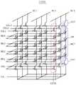
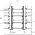
도 2를 참조하면, 제1 저항 메모리 소자(1)는 기판(100) 상에 배치된 게이트 스택(20), 게이트 스택(20)을 관통하여 기판(100)과 전기적으로 연결되는 채널(140), 채널(140)을 따라 연장되어 채널(140)과 접하는 가변저항막(150), 그리고 채널(140)과 전기적으로 연결된 비트라인(190)을 포함할 수 있다. 제1 저항 메모리 소자(1)는 인접한 게이트 스택들(20) 사이에 그리고 게이트 스택(20)과 비트라인(190) 사이에 제공된 층간절연막(170), 그리고 층간절연막(170)을 관통하여 채널(140)과 비트라인(190)을 전기적으로 연결하는 플러그(180)를 더 포함할 수 있다.Referring to Figure 2, a first
기판(100)은 제1 도전형(예: P형)으로 도핑된 단결정 실리콘 웨이퍼를 포함할 수 있다. 기판(100)은 인접한 게이트 스택들(20) 사이에 공통 소오스(101)를 포함할 수 있다. 공통 소오스(101)는 기판(100)과 반대되는 제2 도전형(예: N형)으로 도핑될 수 있다. 공통 소오스(101)는 비트라인(190)의 연장방향(예: 좌우방향)과 대체로 직교하는 방향(예: 전후방향)으로 연장될 수 있다.The
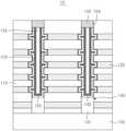
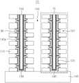
게이트 스택(20)은 채널(140)의 연장방향(예: 수직방향)을 따라 교대로 적층된 몰드절연막들(110)과 게이트들(160)을 포함할 수 있다. 게이트 스택(20), 게이트 스택(20)을 관통하는 채널(140), 채널(140)과 접하는 가변저항막(150)은 셀 스트링(CSTR)을 구성할 수 있다. 본 발명을 이에 한정하려는 의도는 전혀 아닌 단지 일례로서 도 2에는 하나의 비트라인(190)에 병렬 연결된 두 개의 셀 스트링들(CSTR)이 도시되어 있다.The
게이트들(160) 중 최하층의 제1 게이트(161)는 공통 소오스(101)와 채널(140) 간의 전기적 연결을 제어하는 접지 선택라인(GSL), 최상층의 제6 게이트(166)는 비트라인(190)과 채널(140) 간의 전기적 연결을 제어하는 스트링 선택라인(SSL1~SSL3), 그리고 중간층의 제2 내지 제5 게이트들(162~165)은 실질적으로 정보를 저장할 수 있는 워드라인들(WL1~WL4)을 구성할 수 있다. 게이트들(160)은 제1 수평방향(예: 전후방향)으로, 그리고 비트라인(190)은 제1 수평방향과 대체로 직교하는 제2 수평방향(예: 좌우방향)으로 연장될 수 있다. 게이트들(160)은 서로 동일하거나 유사한 두께(수직길이)를 가질 수 있다. 제2 내지 제5 게이트들(162~165)은 메모리 셀을, 제1 및 제6 게이트들(161,166)은 비메모리 셀들을 구성할 수 있다. 제1 게이트(160) 및 제6 게이트(160) 각각은 하나의 도전막 혹은 복수개(예: 2개)의 도전막들을 포함할 수 있다.The lowest gate
몰드절연막들(110)은 기판(100)과 제1 게이트(161) 사이의 제1 몰드절연막(111), 제1 게이트(161)와 제6 게이트(165) 사이의 제2 내지 제6 몰드절연막들(112~116), 그리고 제6 게이트(166) 상의 제7 몰드절연막들(117)을 포함할 수 있다. 몰드절연막들(110)은 동일하거나 유사한 두께를 가지거나 혹은 서로 다른 두께를 가질 수 있다. 일례로, 몰드절연막들(110) 중에서 제2 몰드절연막(112)과 제6 몰드절연막(116)은 상대적으로 큰 두께를 가질 수 있다.The
도 1을 더 참조하면, 비트라인(190)은 BL1~BL3 중에서 어느 하나, 가변저항막(150)은 VR, 그리고 공통 소오스(101)는 CSL에 상당할 수 있다. 가령, 우측의 셀 스트링(CSTR)의 게이트 스택(20)에 있어서, 비트라인(190)은 BL1, 제1 게이트(161)는 GSL, 제6 게이트(166)는 SSL1, 그리고 제2 내지 제5 게이트들(162~165)은 GSL과 SSL1 사이의 WL1~WL4에 상당할 수 있다. 좌측의 셀 스트링(CSTR)에 있어서, 비트라인(190)은 BL2, 제1 게이트(161)는 GSL, 제6 게이트(166)는 SSL2, 그리고 제2 내지 제5 게이트들(162~165)은 GSL2와 SSL2 사이의 WL1~WL4에 상당할 수 있다.1, the
채널(140)은 그 하단이 기판(100)과 전기적으로 연결되고 그 상단은 비트라인(190)과 전기적으로 연결될 수 있다. 채널(140)은 하단이 닫히고 상단이 열린 컵 형태를 가질 수 있다. 예를 들면, 채널(140)은 불순물이 도핑되지 않거나 혹은 기판(100)과 동일하게 제1 도전형(예: P형)으로 도핑된 단결정 혹은 다결정 실리콘을 포함할 수 있다. 채널(140)의 상단은 플러그(180)를 통해 비트라인(190)과 전기적으로 연결되는 드레인(102)으로 정의될 수 있다. 드레인(102)은 공통 소오스(101)와 동일하게 제2 도전형(예: N형)으로 도핑될 수 있다. 채널(140)과 게이트(160) 사이에 가령 실리콘산화막과 같은 게이트 절연막(130)이 제공될 수 있다. 일례로, 게이트 절연막(130)은 게이트 스택(20)을 관통하는 연속적인 형태를 가질 수 있다.The
가변저항막(150)은 채널(140)과 동일 또는 유사하게 하단은 닫히고 상단은 열린 컵 형태를 가질 수 있다. 이 경우, 가변저항막(150)의 컵 형태의 내부에 매립절연막(155)이 제공될 수 있다. 매립절연막(155)은 실리콘산화막을 포함할 수 있다. 다른 예로, 가변저항막(150)은 속이 찬 기둥 형태를 가질 수 있고, 이 경우엔 매립절연막(155)이 형성되지 않을 수 있다. 가변저항막(150)은 인가된 전기장의 방향 및/또는 세기, 혹은 가변저항막(150)의 양단에 걸린 전압차에 따라 내부 저항이 바뀌는 전이금속산화막을 포함할 수 있다. 예를 들면, 가변저항막(150)은 지르코늄(Zr), 하프늄(Hf), 알루미늄(Al), 니켈(Ni), 구리(Cu), 몰리브덴(Mo), 탄탈륨(Ta), 타이타늄(Ti), 텅스텐(W), 크롬(Cr), 스트론튬(Sr), 란탄(La), 망간(Mn), 칼슘(Ca), 프라세오디뮴(Praseodymium, Pr)을 포함하는 그룹에서 선택되는 적어도 하나의 산화막을 포함할 수 있다.The
본 실시예에 따르면, 게이트들(160)은 기판(100)의 상면과 평행한 측방향으로 리세스될 수 있다. 게이트들(160)의 리세스에 의해 게이트 절연막(130)과 채널(140)은 구불구불하게 연장될 수 있다. 가변저항막(150)은 게이트들(160)을 향해 돌출된 돌출부(150p)를 포함할 수 있다. 이하에서 제1 저항 메모리 소자(1)의 셀(91)에 대해 도 3a를 참조하여 상세히 설명한다.
According to the present embodiment, the
<실시예 1의 셀 구조><Cell structure of Example 1>
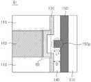
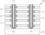
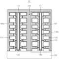
도 3a는 본 발명의 일 실시예에 따른 저항 메모리 소자의 셀 일부를 확대 도시한 단면도이다. 도 3b 내지 3d는 도 3a의 변형예를 도시한 단면도이다. 이하에선 제3 게이트(163)에 해당하는 셀에 대해 설명하며, 이는 다른 게이트들(160)에 해당하는 셀들에 해당될 수 있다.3A is an enlarged cross-sectional view of a portion of a cell of a resistance memory device according to an embodiment of the present invention. Figs. 3B to 3d are sectional views showing a modification of Fig. 3A. Hereinafter, a cell corresponding to the
도 3a를 도 2와 같이 참조하면, 제3 게이트(163)는 기판(100)의 상면과 평행한 방향(예: 좌우방향)으로 리세스되고, 이에 따라 제3 게이트(163)의 측면(163s)은 제3 몰드절연막(113)의 측면(113s) 및 제4 몰드절연막(110)의 측면(114s)과 공면을 이루지 아니할 수 있다. 다시 말해, 제3 게이트(163의 측면(163s)은 제3 몰드절연막(113) 및 제4 몰드절연막(114)의 측면들(113s,114s)과 수직 정렬되지 않을 수 있다.Referring to FIG. 3A, the
제3 게이트(163)의 리세스는 제3 몰드절연막(113)과 제4 몰드절연막(114) 사이에 벽감(80: alcove)을 형성할 수 있다. 게이트 절연막(130)은 수직방향과 수평방향으로 반복 연장되는 형태를 가질 수 있다. 가령, 게이트 절연막(130)은 제3 몰드절연막(113)의 측면(113s)을 따라 수직하게 연장되고, 벽감(80)의 내면을 따라 브라켓 형태로 연장되고, 그리고 제4 몰드절연막(114)의 측면(114s)을 따라 수직하게 연장될 수 있다. 게이트 절연막(130)은 그 연장방향을 따라 실질적으로 동일한 두께를 가질 수 있다. 다른 예로, 게이트 절연막(130)은 제3 게이트(163)의 측면(163s)과 접하는 부분이 다른 부분에 비해 큰 두께를 가질 수 있다.The recess of the
채널(140)은 게이트 절연막(130)과 동일 또는 유사하게 수직방향과 수평방향으로 반복 연장되는 형태를 가질 수 있다. 가령 채널(140)은 제3 몰드절연막(113)과 제4 몰드절연막(114)의 측면들(113s,114s)을 따라 수직한 형태로 그리고 벽감(80)의 내면을 따라 브라켓 형태로 연장될 수 있다. 그러므로, 제3 게이트(163)는 채널(140)의 길이(Lc)에 비해 클 수 있다. 소자의 축소화에 의해 몰드절연막들(113,114) 사이의 간격이 줄어들어 채널(140)의 길이(Lc)가 축소되더라도 상대적으로 큰 게이트 길이(Lg)를 가질 수 있어 트랜지스터의 신뢰성을 확보할 수 있다. 채널(140)은 그 연장방향을 따라 실질적으로 동일한 두께를 가질 수 있다. 다른 예로, 채널(140)은 제3 게이트(163)의 측면(163s)과 오버랩된 부분이 다른 부분에 비해 크거나 작은 두께를 가질 수 있다.The
가변저항막(150)은 제3 몰드절연막(113)과 제4 몰드절연막(114)의 측면들(113s,114s)을 따라 수직하게 연장될 수 있다. 본 실시예에 따르면, 가변저항막(150)은 벽감(80)을 향해 신장된 돌출부(150p)를 포함할 수 있다. 가변저항막(150)의 돌출부(150p)는 채널(140)의 수직하게 연장된 부분을 가로질러 벽감(80)의 내부로 삽입될 수 있다. 벽감(80) 내부로 삽입된 가변저항막(150)의 돌출부(150p)는 제3 몰드절연막(113)과 제4 몰드절연막(114)과 상하 오버랩될 수 있다. 이 경우 가변저항막(150)의 돌출부(150p)의 길이는 채널(130)의 두께에 비해 클 수 있다. 본 실시예에 따르면, 채널(140)은 전체적으로 수직하게 연장되지 아니하지만, 전류의 흐름(실선화살표)은 가변저항막(150)의 돌출부(150p)를 관통하여 채널(140)을 따라 수직할 수 있다.The variable
도 4b에서 후술한 것처럼 가변저항막(150)의 돌출부(150p)에 전기적 경로로 제공되는 필라멘트(도 4b의 150f)가 생성될 수 있다. 따라서, 돌출부(150p)에 미치는 전기장의 방향을 바꾸므로써 셀(91)의 저항의 상태를 스위칭하여 셀(91)에 정보를 저장하거나 지울 수 있다. 돌출부(150p)의 두께(Tp)를 축소할 수 있으므로 필라멘트(도 4b의 150f)의 생성이 용이해질 수 있고, 이에 따라 용이한 스위칭이 가능할 수 있다. 그리고, 돌출부(150p)에 균일한 전기장이 미칠 수 있어 전기적 특성이 향상될 수 있다.A filament (150f in Fig. 4B) provided in an electrical path can be generated on the
도 3b를 참조하면, 산소교환막(151)과 배리어막(152) 중 적어도 어느 하나가 더 제공될 수 있다. 산소교환막(151)은 가변저항막(150)에 포함된 것과 동일한 전이금속을 포함하는 산화막일 수 있다. 산소교환막(151)은 가변저항막(150)과 산소들을 주고받을 수 있다. 예를 들어 쓰기 동작시, 가변저항막(150) 내의 전이금속과 결합된 산소들의 일부가 빠져나가(즉, 전이금속의 환원) 가변저항막(150)은 고저항 상태에서 저저항 상태로 변할 수 있다. 이때, 산소들은 가변저항막(150)에서 산소교환막(151)으로 이동될 수 있다. 지우기 동작시, 산소교환막(151)에 포함된 산소들이 가변저항막(150)으로 이동되어 가변저항막(150) 내의 전이금속과 결합하고(즉, 전이금속의 산화) 가변저항막(150)은 저저항 상태에서 고저항 상태로 변할 수 있다. 배리어막(152)은 가변저항막(150)에 포함된 것과 상이한 전이금속을 포함하는 산화막일 수 있다. 배리어막(152)은 가변저항막(150)에 포함된 산소들이 채널(140)로 이동되는 것을 막을 수 있다. 배리어막(152)은 채널(140)과 가변저항막(150) 사이에, 산소교환막(151)은 가변저항막(150)과 매립절연막(155) 사이에 혹은 배리어막(152)과 가변저항막(150) 사이에 배치될 수 있다.Referring to FIG. 3B, at least one of the
도 3c를 참조하면, 가변저항막(150)의 돌출부(150p)는 채널(140)의 수직 부분을 가로지르되 벽감(80)의 내부로 삽입되지 아니할 수 있다. 일례로, 가변저항막(150)의 돌출부(150p)는 채널(140)의 수직 부분의 두께(D)와 동일 또는 유사한 길이(L1)를 가질 수 있다. 일례에 따르면, 가변저항막(150)의 돌출부(150p)는 제3 몰드절연막(113)과 제4 몰드절연막(114)과 상하 오버랩되지 않을 수 있다.3C,
도 3d를 참조하면, 가변저항막(150)의 돌출부(150p)는 벽감(80)의 내부로 삽입되지 아니하고 채널(140)의 수직 부분을 일부 가로지르도록 신장될 수 있다. 일례로, 가변저항막(150)의 돌출부(150p)는 채널(140)의 수직 부분의 두께(D)보다 작은 길이(L2)를 가질 수 있다.The
셀(91)의 구조는 도 3a 내지 3d에 제한되지 아니하며 후술한 바와 같이 다양한 구조를 가질 수 있다.
The structure of the
<실시예 1의 동작>≪ Operation of
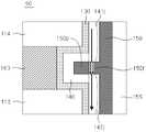
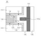
도 4a는 본 발명의 일 실시예에 따른 저항 메모리 소자의 일부를 도시한 단면도이다. 도 4b는 본 발명의 일 실시예에 따른 저항 메모리 소자에 있어서 선택 셀을 도시한 단면도이다. 도 4c는 도 4b와 등가 구조를 도시한 단면도이다.4A is a cross-sectional view illustrating a portion of a resistive memory device according to an embodiment of the present invention. 4B is a cross-sectional view illustrating a selected cell in a resistance memory device according to an embodiment of the present invention. 4C is a sectional view showing an equivalent structure to FIG. 4B.
도 4a를 도 1과 같이 참조하면, 비트라인(BL1)과 공통 소오스 라인(CSL) 사이의 셀 스트링(60)을 선택하고, 그 셀 스트링(60)에서 제2 워드라인(WL2)이 속한 셀(90)을 선택한 경우를 가정한다. 쓰기 및 지우기 동작시 선택 셀(90)의 저항이 바뀌도록 하고, 그 저항에 따른 전류 세기를 읽게 하여 읽기 동작을 할 수 있다.Referring to FIG. 4A, the
쓰기 동작의 경우, 선택 셀(90)에는 문턱전압(Vth)보다 낮은 전압(예: 0V)을 걸어 턴-오프시키고, 비선택 셀들에는 문턱전압보다 큰 전압(Vpass)을 걸어 턴-온시키고, 공통 소오스(101)는 접지하고, 그리고 비트라인(190)에는 선택 셀(90)이 저저항 상태로 바뀔 수 있는 전압(+V)을 인가할 수 있다. 비선택된 셀 스트링들과 전기적으로 연결된 비트라인들(BL2,BL3)에는 공통 소오스(101)와 동일한 전압(0V)을 걸어줄 수 있다. 상기 쓰기 전압 조건은 단지 일례이지 본발명을 이에 한정하려는 의도는 전혀 아니다.In the case of the write operation, a voltage (for example, 0 V) lower than the threshold voltage Vth is applied to the selected
도 4b를 참조하면, 상기 쓰기 전압 조건에 의해 제3 게이트(163)에 인접한 채널(140)에는 제3 게이트(163)와 이에 인접한 제2 게이트(162) 및 제4 게이트(164) 사이의 프린지 필드(fringe field)와 같은 전기장에 의해 접합영역들(141j,142j)이 형성될 수 있다. 제1 접합영역(141j)에는 비트라인(190)에 인가된 전압(+V)이 걸릴 수 있고, 제2 접합영역(142j)에는 공통 소오스(101)에 걸린 전압(0V)이 걸릴 수 있다. 제1 접합영역(141j)과 제2 접합영역(142j) 사이에 발생한 전압차에 의해 가변저항막(150)의 돌출부(150p)에 전기장(점선화살표)이 형성될 수 있다. 상기 전기장에 의해 가변저항막(150)의 돌출부(150p) 내에 포함된 산소들이 다른 곳으로 이동하여 전이금속으로 환원되고, 전이금속의 환원에 의해 가변저항막(150)의 돌출부(150p)를 수직하게 관통하는 필라멘트(150f)와 같은 전기적 경로가 형성될 수 있다. 필라멘트(150f)가 형성된 선택 셀(90)을 데이터 '1'이 저장된 것 혹은 'ON' 상태로 간주할 수 있다.Referring to FIG. 4B, in the
도 4a에 도시된 것처럼, 선택된 셀 스트링(60)에서의 전류 흐름(실선화살표)은 비선택 셀들에서는 브라켓 형태의 채널(140)을 따라 구불구불하고, 도 4b에 도시된 바와 같이 선택 셀(90)에서는 가변저항막(150)의 돌출부(150p)에 형성된 필라멘트(150f)를 관통하므로써 수직할 수 있다.4A, the current flow (solid line arrow) in the selected
가변저항막(150)이 접합영역들(141j,142j)의 측면에 배치되어 있더라도 제1 접합영역(141j)과 제2 접합영역(142j) 사이의 돌출부(150p)에 필라멘트(150f)가 형성될 수 있다. 그러므로 선택 셀(90)은 도 4c에 도시된 것처럼 상부전극(41j)과 하부전극(42j) 사이에 배치된 가변저항막(50)에 수직한 전기장(점선화살표)에 의해 필라멘트(50f)가 생성되어 수직한 전류 흐름(실선화살표)을 갖는 셀(90c)과 등가일 수 있다.The
지우기 동작의 경우, 선택 셀(90)에는 턴-오프에 필요한 전압(예: 0V)을 인가하고, 비선택 셀들에는 턴-온에 필요한 전압(Vpass)을 인가하고, 비트라인(190)은 접지하고, 그리고 공통 소오스(101)에는 선택 셀(90)이 고저항 상태로 바뀔 수 있는 전압(+V)을 인가할 수 있다. 비선택된 셀 스트링들과 전기적으로 연결된 비트라인들(BL2,BL3)에는 공통 소오스(101)와 동일한 전압(+V)을 걸어줄 수 있다. 상기 지우기 전압 조건은 단지 일례이지 본발명을 이에 한정하려는 의도는 전혀 아니다.In the case of the erase operation, the voltage (for example, 0 V) required for turn-off is applied to the selected
상기 지우기 전압 조건에 의해 제1 접합영역(141j)에는 비트라인(190)에 인가된 전압(예: 0V)이 걸리고 제2 접합영역(142j)에는 공통 소오스(101)에 인가된 전압(+V)이 걸릴 수 있다. 제1 접합영역(141j)과 제2 접합영역(142j) 사이에 발생한 전압차에 의해 전기장 방향이 바뀌게 되고, 산소들이 필라멘트(150f)를 이루던 전이금속들로 이동되어 전이금속들이 산화될 수 있다. 이로써, 가변저항막(150)의 돌출부(150p)에 형성되어 있던 필라멘트(150f)가 사라질 수 있다. 필라멘트(150f)가 사라진 선택 셀(90)을 데이터 '0'이 저장된 것 혹은 'OFF' 상태로 간주할 수 있다.A voltage (for example, 0 V) applied to the
읽기 동작의 경우, 선택 셀(90)에는 턴-오프에 필요한 전압(예: 0V)을 인가하고, 비선택 셀들에는 턴-온에 필요한 전압(Vpass)을 인가하고, 공통 소오스(101)는 접지하고, 그리고 비트라인(190)에는 선택 셀(90)의 저항 상태를 감지할 수 있는 전압(Vread)을 인가할 수 있다. 비선택된 셀 스트링들과 전기적으로 연결된 비트라인들(BL2,BL3)에는 공통 소오스(101)와 동일한 전압(0V)을 걸어줄 수 있다. 상기 읽기 전압 조건은 단지 일례이지 본발명을 이에 한정하려는 의도는 전혀 아니다.In the case of a read operation, a voltage (for example, 0 V) required for turn-off is applied to the selected
상기 읽기 전압 조건에 의해 선택 셀(90)에 필라멘트(150f)가 형성된 경우 전류 흐름(실선화살표)이 감지될 수 있다. 이 경우 선택 셀(90)에 데이터 '1'이 저장되어 있음을 알 수 있다. 이와 다르게, 선택 셀(90)에 필라멘트(150f)가 없는 경우 전류는 감지되지 않을 수 있다. 이 경우 선택 셀(90)에 데이터 '0'이 저장되어 있음을 알 수 있다.When the
본 실시예에 따르면, 선택 셀(90)이 포함된 셀 스트링(60)의 양단의 극성을 뒤바꾸므로써 바이폴라 스위칭(bipolar switching)이 가능할 수 있다. 가령 선택 셀(90)이 포함된 셀 스트링(60)에 전기적으로 연결된 공통 소오스(101)와 비트라인(190)에 걸린 전압을 뒤바꿈으로써 쓰기 및 지우기 동작이 가능할 수 있다. 이에 반해, 유니폴라 스위칭(unipolar switching) 방식의 저항 메모리 소자는 한쪽 극성 전압의 크기를 달리하므로써 스위칭이 가능할 수 있다. 그러므로, 본 실시예의 바이폴라 스위칭이 가능한 저항 메모리 소자는 유니폴라 스위칭이 가능한 저항 메모리 소자에 비해 상대적으로 작은 전류로 동작이 가능할 수 있다.
According to the present embodiment, bipolar switching may be possible by reversing the polarity of both ends of the
<실시예 1의 제조방법>≪ Production method of Example 1 >
도 5a 내지 5j는 본 발명의 일 실시예에 따른 저항 메모리 소자의 제조방법을 도시한 단면도들이다.5A to 5J are cross-sectional views illustrating a method of manufacturing a resistance memory device according to an embodiment of the present invention.
도 5a를 참조하면, 기판(100) 상에 수직홀(103)을 갖는 몰드 스택(10)을 형성할 수 있다. 기판(100)은 가령 제1 도전형(예: N형)으로 도핑된 단결정 실리콘 웨이퍼를 포함할 수 있다. 몰드 스택(10)은 식각선택비가 상이한 몰드절연막들(110)과 몰드희생막들(120)을 교대로 적층하여 형성할 수 있다. 일례로, 몰드절연막들(110)은 실리콘산화막(예: SiOx)을 몰드희생막들(120)은 실리콘질화막(예: SiNx)을 증착하여 형성할 수 있다. 몰드 스택(10)을 이방성 식각하여 기판(100)을 노출시키는 수직홀(103)을 형성할 수 있다.Referring to FIG. 5A, a
도 5b를 참조하면, 기판(100)의 상면과 평행한 방향(예: 좌우방향)을 따라 몰드희생막들(120)을 리세스시킬 수 있다. 일례로, 몰드희생막들(120)을 선택적으로 제거할 수 있는 에천트의 제공으로 수직홀(103)을 통해 노출된 몰드희생막들(120)의 측면들(120s)을 식각할 수 있다. 이에 따라 수직홀(103)을 통해 노출된 몰드희생막들(120)의 측면들(120s)과 몰드절연막들(110)의 측면들(110s)은 공면을 이루지 않을 수 있다. 몰드희생막들(120)의 리세스에 의해 수직홀(103)의 내표면은 벽감(80)을 갖는 울퉁불퉁한 형태를 가질 수 있다.Referring to FIG. 5B, the mold
도 5c를 참조하면, 게이트 절연막(130)을 형성할 수 있다. 게이트 절연막(130)은 절연체의 증착과 선택적 식각으로 수직홀(103)의 내측면을 따라 연장된 형태로 형성할 수 있다. 가령, 화학기상증착으로 몰드 스택(10)을 덮는 실리콘산화막을 증착하고 기판(100)의 상면이 노출되도록 이방성 식각하여 게이트 절연막(130)을 형성할 수 있다. 상기 이방성 식각에 의해 최상층의 몰드절연막(110) 상에 증착된 실리콘산화막이 제거될 수 있다. 수직홀(103)의 내표면은 벽감(80)을 가지고 있기 때문에 게이트 절연막(130)은 수직홀(103)의 내표면의 프로파일을 따라 울퉁불퉁한 형태를 가질 수 있다.Referring to FIG. 5C, a
도 5d를 참조하면, 수직홀(103) 내에 반도체막(140a)과 전이금속산화막(150a)을 형성할 수 있다. 예컨대, 반도체막(140a)은 불순물이 도핑되지 않거나 혹은 기판(100)과 동일하게 제1 도전형(예: P형)으로 도핑된 단결정 혹은 다결정 실리콘을 증착하여 형성할 수 있다. 전이금속산화막(150a)은 지르코늄(Zr), 하프늄(Hf), 알루미늄(Al), 니켈(Ni), 구리(Cu), 몰리브덴(Mo), 탄탈륨(Ta), 타이타늄(Ti), 텅스텐(W), 크롬(Cr), 스트론튬(Sr), 란탄(La), 망간(Mn), 칼슘(Ca), 프라세오디뮴(Pr)을 포함하는 그룹에서 선택된 적어도 하나의 산화막을 증착하여 형성할 수 있다. 반도체막(140a)과 전이금속산화막(150a)은 몰드 스택(10)의 프로파일을 따라 연속적으로 연장되어 최상층의 몰드절연막(110)을 덮는 형태로 형성할 수 있다.Referring to FIG. 5D, the
선택적으로 전이금속산화막(150a)은 수직홀(103)을 완전히 채우지 않는 컵 형태로 형성할 수 있다. 이 경우 전이금속산화막(150a)의 컵 형태의 내부를 채우는 절연막(155a)을 더 형성할 수 있다. 절연막(155a)은 실리콘산화막을 증착하여 전이금속산화막(150a)을 덮는 형태로 형성할 수 있다. 다른 예로, 전이금속산화막(150a)은 수직홀(103)을 완전히 채우는 기둥 형태로 형성할 수 있다. 이 경우엔 절연막(155a)을 형성하는 것을 스킵할 수 있다.Alternatively, the transition
도 5e를 참조하면, 평탄화 공정으로 채널(140)과 가변저항막(150)을 형성할 수 있다. 가령 절연막(155a)과 전이금속산화막(150a) 그리고 반도체막(140a)을 화학기계적 연마하거나 에치백하여 최상층의 몰드절연막(110)이 노출되도록 평탄화할 수 있다. 이에 따라, 수직홀(103) 내에는 몰드 스택(10)을 수직 관통하여 몰드희생막들(120) 및 몰드절연막들(110)과 접하는 게이트 절연막(130), 하단은 닫히고 상단은 열린 컵 형태를 가지며 기판(100)과 전기적으로 연결된 채널(140), 그리고 매립절연막(155)에 의해 내부가 채워진 컵 형태를 갖는 가변저항막(150)이 형성될 수 있다. 일 실시예에 따르면, 몰드절연막들(110) 사이에 벽감(80)이 형성되어 있기 때문에, 채널(140)은 벽감(80)의 내면을 따라 연장된 브라켓 형태를 포함하고 가변저항막(150)은 벽감(80)을 향해 신장된 돌출부(150p)를 포함할 수 있다.Referring to FIG. 5E, the
도 5f를 참조하면, 몰드 스택(10)을 관통하는 트렌치(105)를 형성할 수 있다. 일례로, 이방성 식각으로 몰드 스택(10)을 패터닝하여 기판(100)을 노출시키는 트렌치(105)를 형성할 수 있다. 트렌치(105)는 몰드절연막들(110)과 몰드희생막들(120)의 측벽들을 노출시킬 수 있다. 트렌치(105)는 기판(100)을 가로지르는 방향(예: 전후방향)으로 연장된 라인 형태일 수 있다. 몰드 스택(10)은 트렌치(105)의 연장방향과 동일한 방향(예: 전후방향)으로 연장된 라인 형태를 가질 수 있다.Referring to FIG. 5F, a
도 5g를 참조하면, 가변저항막(150)을 따라 몰드절연막들(110)이 수직으로 이격 배열된 몰드 윙(15)을 형성할 수 있다. 일례로, 트렌치(105)를 통해 에천트를 제공하는 등방성 식각으로 몰드희생막들(120)을 선택적으로 제거할 수 있다. 상기 등방성 식각에 있어서 몰드절연막들(110)이 실리콘산화막이고 몰드희생막들(120)이 실리코질화막이면 에천트로서 인산(H3PO4)을 채택할 수 있다. 몰드희생막들(120)의 선택적 식각에 의해 몰드절연막들(110) 사이에는 게이트 절연막(130)을 노출시키는 스페이스들(107)이 형성될 수 있다.Referring to FIG. 5G, the
도 5h를 참조하면, 몰드 윙(15)을 덮는 도전막(160a)을 형성할 수 있다. 가령, 기판(100) 상에 실리콘, 금속, 금속질화물, 금속실리사이드 등을 증착하여 도전막(160a)을 형성할 수 있다. 도전막(160a)은 트렌치(105)와 스페이스들(107)을 매립할 수 있다.Referring to FIG. 5H, a
도 5i를 참조하면, 몰드절연막들(110) 사이에 게이트들(160)이 형성된 게이트 스택(20)을 형성할 수 있다. 가령, 도전막(160a)을 평탄화한 후 이방성 식각으로 패터닝하여 스페이스들(107)을 채우는 게이트들(160)을 형성할 수 있다. 트렌치(105)를 통해 노출된 기판(100)에 불순물을 주입하여 기판(100)과 다른 제2 도전형(예: N형)으로 도핑된 공통 소오스(101)를 형성할 수 있다. 채널(140)의 상단부에 불순물을 주입하여 공통 소오스(101)와 동일한 제2 도전형(예: N형)으로 도핑된 드레인(102)을 형성할 수 있다. 공통 소오스(101)와 드레인(102)은 동시에 형성할 수 있다. 복수개의 공통 소오스들(101)은 서로 전기적으로 연결되어 전압 인가시 등전위 상태를 가질 수 있다. 게이트들(160)과 공통 소오스(101)는 트렌치(105)의 연장방향과 동일한 방향(예: 전후방향)으로 연장될 수 있다.Referring to FIG. 5I, a
도 5j를 참조하면, 기판(100) 상에 층간절연막(170)을 형성하고 층간절연막(170) 상에 드레인(102)과 전기적으로 연결된 비트라인(190)을 형성할 수 있다. 예컨대, 기판(100) 상에 실리콘산화막을 증착하여 트렌치(105)를 매립하며 게이트 스택(20)을 덮는 층간절연막(170)을 형성할 수 있다. 층간절연막(170)을 관통하여 드레인(102)과 연결된 플러그(180)를 형성하고, 층간절연막(170) 상에 플러그(180)와 연결된 비트라인(190)을 형성할 수 있다. 비트라인(190)은 게이트들(160)의 연장방향(예: 전후방향)과 교차하는 방향(예: 좌우방향)으로 연장될 수 있다. 다른 예로, 기판(100) 상에 게이트 스택(20)을 덮는 절연체를 증착한 후 평탄화하여 트렌치(105)를 매립하는 절연막을 형성하고, 그리고 평탄화된 그 절연막 상에 또 다른 절연막을 더 층착하여 층간절연막(170)을 형성할 수 있다. 상기 일련의 공정들을 통해 도 2에 도시된 바와 같은 제1 저항 메모리 소자(1)를 제조할 수 있다.
Referring to FIG. 5J, an
<실시예 2>≪ Example 2 >
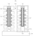
도 6a 내지 6e는 본 발명의 다른 실시예에 따른 저항 메모리 소자의 제조방법을 도시한 단면도들이다. 이하에선 실시예 1과 상이한 점에 대해 상설하고 동일한 점에 대해서는 개설하거나 생략하기로 하며, 이는 다른 실시예들에 대해서도 마찬가지다.6A to 6E are cross-sectional views illustrating a method of manufacturing a resistance memory device according to another embodiment of the present invention. The following points are different from the first embodiment and the same points will be described or omitted, which is also true for the other embodiments.
도 6a를 참조하면, 몰드 스택(10)을 관통하는 수직홀(103)을 형성하고 수직홀(103)의 하단부에 제1 반도체막(141)을 형성할 수 있다. 제1 반도체막(141)은 수직홀(103)을 통해 노출된 기판(100)으로부터 실리콘을 에피 성장시키거나 혹은 증착하여 형성할 수 있다. 제1 반도체막(141)은 불순물이 도핑되지 않거나 혹은 기판(100)과 동일하게 제1 도전형(예: P형)으로 도핑된 단결정 혹은 다결정 실리콘일 수 있다. 제1 반도체막(141)은 최하층의 몰드희생막(120)과 좌우 오버랩될 수 있다. 그리고, 몰드희생막들(120)을 리세스하여 몰드절연막들(110) 사이에 벽감(80)을 형성하고, 수직홀(103)의 내측면을 따라 연장되는 게이트 절연막(130)을 형성할 수 있다. 게이트 절연막(130)은 실리콘산화막의 증착과 이방성 식각으로 형성할 수 있다.Referring to FIG. 6A, a
다른 예로, 몰드 스택(10)은 2회로 나누어 형성할 수 있다. 예컨대, 기판(100) 상에 2개의 몰드절연막들(110) 사이에 몰드희생막(120)이 배치된 하부스택(10b)을 형성하고, 하부스택(10b)을 관통하여 기판(100)을 노출시키는 하부 홀(103b)을 형성하고, 하부 홀(103b)이 채워지도록 실리콘을 에피 성장시키거나 증착하여 제1 반도체막(141)을 형성할 수 있다. 하부스택(10b) 상에 몰드절연막들(110)과 몰드희생막들(120)을 교대로 적층하여 상부스택(10t)을 형성하고, 상부스택(10t)을 관통하여 제1 반도체막(141)을 노출시키는 수직홀(103)을 형성하고, 수직홀(103)을 통해 노출된 몰드희생막들(120)을 리세스하여 벽감(80)을 형성할 수 있다.As another example, the
도 6b를 참조하면, 수직홀(103) 내에 하단은 닫히고 상단은 열린 컵 형태를 가지며 제1 반도체막(141)과 연결된 제2 반도체막(142), 그리고 매립절연막(155)에 의해 내부가 채워진 컵 형태를 갖는 가변저항막(150)을 형성할 수 있다. 수직홀(103)의 상단부에 드레인(102)을 형성할 수 있다. 제2 반도체막(142)은 제1 반도체막(141)과 동일한 물질일 수 있다. 제1 반도체막(141)과 제2 반도체막(142)은 채널(140)을 구성할 수 있다. 드레인(102)은 채널(140)과 가변저항막(150)과 매립절연막(155)의 상단부들을 식각하여 홀(104)을 형성하고, 그 홀(104)을 불순물로 도핑된 실리콘으로 채워 형성할 수 있다. 다른 예로, 도 5i에서와 같이 채널(140)의 상단부에 불순물을 주입하여 드레인(102)을 형성할 수 있다.Referring to FIG. 6B, the
도 6c를 참조하면, 몰드 스택(10)을 관통하여 기판(100)을 노출시키는 트렌치(105)를 형성하고, 그리고 트렌치(105)를 통해 노출된 몰드희생막들(120)을 제거하여 몰드 윙(15)을 형성할 수 있다. 본 실시예에 따르면, 스페이스들(107)을 통해서 채널(140)의 일부와 게이트 절연막(130)이 노출될 수 있다. 가령, 벌크 구조를 갖는 채널(140)의 하단 측면(141s)이 노출될 수 있다.6C, a
도 6d를 참조하면, 노출된 채널(140)의 측면(141s)을 열처리 공정으로 산화시켜 제2 게이트 절연막(135)을 형성할 수 있다. 상기 열처리 공정시 트렌치(105)를 통해 노출된 기판(100)이 산화되어 절연막(130a)이 형성될 수 있다. 드레인(102)은 트렌치(105)를 형성하기 위한 마스크(70)로 가려질 수 있어 절연막이 형성되지 않을 수 있다.Referring to FIG. 6D, the
도 6e를 참조하면, 도 5h 내지 5j에서 설명한 바와 동일 또는 유사한 공정으로 제2 저항 메모리 소자(2)를 제조할 수 있다. 셀(92)은 도 3a에 도시된 셀(91)과 실질적으로 동일할 수 있다.Referring to FIG. 6E, the second
본 실시예에 따르면, 가변저항막(150)은 접지 선택라인(GSL)을 구성하는 최하층의 게이트(160)를 제외한 다른 게이트들(160)과 좌우 오버랩될 수 있다. 따라서, 접지 선택라인(GSL)에는 가변저항막(150)이 없을 수 있다. 그러므로, 접지 선택라인(GSL)의 셀(92a)은 다른 셀들(93)과 달리 아일랜드 형태의 제2 게이트 채널(135)이 게이트(160)와 채널(140) 사이에 한정된 구조를 가질 수 있다.According to the present embodiment, the
채널(140)은 최하층의 게이트(160)와 좌우 오버랩되는 벌크 구조가 컵 구조와 연결된 하이브리드 형태를 가질 수 있다. 게이트 절연막(130,135)이 기판(100)의 상면 아래로 침입되어 형성될 염려가 전혀 없으므로 공통 소오스(101)와 채널(140) 간의 전류 흐름이 양호해질 수 있다.
The
<실시예 3>≪ Example 3 >
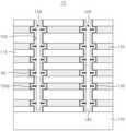
도 7a 내지 7e는 본 발명의 또 다른 실시예에 따른 저항 메모리 소자의 제조방법을 도시한 단면도들이다.7A to 7E are cross-sectional views illustrating a method of manufacturing a resistance memory device according to another embodiment of the present invention.
도 7a를 참조하면, 도 6a 및 6b에서 설명한 바와 동일 또는 유사한 공정으로 제1 몰드 스택(10a)을 형성할 수 있다. 가령, 기판(100) 상에 몰드절연막들(110)과 몰드희생막(120)을 교대로 반복 적층하여 제1 몰드 스택(10a)을 형성하고, 제1 몰드 스택(10a)을 관통하는 수직홀(103)을 형성할 수 있다. 에피 성장 혹은 증착으로 수직홀(103) 내에 기판(100)과 연결되는 제1 반도체막(141)을 형성하고, 수직홀(103)을 통해 노출된 몰드희생막들(120)을 리세스하여 벽감(80)을 형성할 수 있다. 그리고 벽감(80)이 형성된 수직홀(103) 내에 게이트 절연막(130)과 채널(140)과 매립절연막(155)을 형성할 수 있다. 채널(140)은 제1 반도체막(141)과 연결될 수 있다.Referring to FIG. 7A, the
도 7b를 참조하면, 제1 몰드 스택(10a) 상에 몰드절연막들(110) 사이에 몰드희생막(120)이 배치된 제2 몰드 스택(10b)을 형성하고, 그리고 제2 몰드 스택(10b)을 관통하는 제2 수직홀(103b)을 형성할 수 있다. 제2 수직홀(103b)에 의해 적어도 채널(140)이 노출될 수 있다. 이에 따라 제1 몰드 스택(10a) 상에 수직홀(103)과 상하 정렬된 제2 수직홀(103b)을 갖는 제2 몰드 스택(10b)이 적층된 몰드 스택(10)을 형성할 수 있다.7B, a
도 7c를 참조하면, 제2 수직홀(103b)을 제3 반도체막(143)으로 채울 수 있다. 제3 반도체막(143)은 제2 반도체막(142)과 연결될 수 있다. 일 실시예에 따르면, 제1 반도체막(141)과 제2 반도체막(142) 그리고 제3 반도체막(143)은 서로 연결되어 채널(140)을 형성할 수 있다. 제1 반도체막(141)과 제3 반도체막(143)은 벌크 구조를 가질 수 있고, 제2 반도체막(142)은 브라켓 형태를 포함하는 컵 구조를 가질 수 있다. 제3 반도체막(143)의 상단에 불순물을 주입하여 드레인(102)을 형성할 수 있다. 다른 예로, 제3 반도체막(143)을 일부 제거하여 홀(104)을 형성하고, 그 홀(104)은 불순물로 도핑된 실리콘으로 채워 드레인(102)을 형성할 수 있다.Referring to FIG. 7C, the second
도 7d를 참조하면, 몰드 스택(10)을 패터닝하여 트렌치(105)를 형성하고 몰드희생막들(120)을 선택적으로 제거하여 몰드절연막들(110) 사이에 스페이스들(107)이 형성된 몰드 윙(15)을 형성할 수 있다. 스페이스들(107)을 통해 채널(140)의 측면 일부와 게이트 절연막(130)이 노출될 수 있다. 일례로, 벌크 구조를 갖는 채널(140)의 하단 측면(141s) 및 상단 측면(143s)이 노출될 수 있다. 노출된 채널(140)의 측면들(141s,143s)을 열처리하여 산화시킬 수 있다.7D, the
도 7e를 참조하면, 상기 열처리에 의해 채널(140)의 하단과 상단의 측면들에는 제2 게이트 절연막(135)이 형성될 수 있다. 상기 열처리에 의해 기판(100)의 상면이 산화되어 절연막(130a)이 더 형성될 수 있다. 이어서, 도 5h 내지 5j에서 설명한 바와 동일 또는 유사한 공정으로 제3 저항 메모리 소자(3)를 제조할 수 있다. 셀(93)은 도 3a에 도시된 셀(91)과 실질적으로 동일할 수 있다.Referring to FIG. 7E, the second
본 실시예에 따르면, 가변저항막(150)은 최하층의 게이트(160)와 최상층의 게이트(160)를 제외한 다른 게이트들(160)과 좌우 오버랩될 수 있다. 따라서, 접지 선택라인(GSL)과 스트링 선택라인(SSL)에는 가변저항막(150)이 없을 수 있다. 그러므로, 접지 선택라인(GSL)과 스트링 선택라인(SSL)의 셀(93a)은 다른 셀들(93)과 달리 아일랜드 형태의 제2 게이트 채널(135)이 게이트(160)와 채널(140) 사이에 한정된 구조를 가질 수 있다.According to the present embodiment, the
채널(140)은 최하층의 게이트(160)와 최상층의 게이트(160)와 좌우 오버랩되는 벌크 구조가 컵 구조의 상단 및 하단에 연결된 하이브리드 형태를 가질 수 있다.
The
<실시예 4><Example 4>
도 8a 내지 8e는 본 발명의 또 다른 실시예에 따른 저항 메모리 소자의 제조방법을 도시한 단면도들이다.8A to 8E are cross-sectional views illustrating a method of manufacturing a resistance memory device according to another embodiment of the present invention.
도 8a를 참조하면, 도 5a 내지 5e에서 설명한 바와 동일 또는 유사한 공정으로 제1 몰드 스택(10a)을 형성할 수 있다. 가령, 기판(100) 상에 몰드절연막들(110)과 몰드희생막(120)을 교대로 반복 적층하여 제1 몰드 스택(10a)을 형성하고, 제1 몰드 스택(10a)을 관통하며 벽감(80)을 갖는 수직홀(103)을 형성할 수 있다. 수직홀(103) 내에 기판(100)과 연결되는 제1 반도체막(141)과 매립절연막(155)이 내부에 채워진 가변저항막(150)을 형성할 수 있다.Referring to FIG. 8A, the
도 8b를 참조하면, 제1 몰드 스택(10a) 상에 몰드절연막들(110) 사이에 몰드희생막(120)이 배치된 제2 몰드 스택(10b)을 형성하고, 그리고 제2 몰드 스택(10b)을 관통하는 제2 수직홀(103b)을 형성할 수 있다. 제2 수직홀(103b)에 의해 적어도 제1 반도체막(141)이 노출될 수 있다. 이에 따라 제1 몰드 스택(10a) 상에 수직홀(103)과 상하 정렬된 제2 수직홀(103b)을 갖는 제2 몰드 스택(10b)이 적층된 몰드 스택(10)을 형성할 수 있다.8B, a
도 8c를 참조하면, 제2 수직홀(103b)을 제2 반도체막(142)으로 채울 수 있다. 제2 반도체막(142)은 제1 반도체막(141)과 연결될 수 있다. 일 실시예에 따르면, 제1 반도체막(141)은 서로 연결되어 채널(140)을 형성할 수 있다. 제2 반도체막(142)은 벌크 구조를 가질 수 있고, 제1 반도체막(141)은 브라켓 형태를 포함하는 컵 구조를 가질 수 있다. 제2 반도체막(142)의 상단에 불순물을 주입하여 드레인(102)을 형성할 수 있다. 다른 예로, 제2 반도체막(142)을 일부 제거하여 홀(104)을 형성하고, 그 홀(104)은 불순물로 도핑된 실리콘으로 채워 드레인(102)을 형성할 수 있다.Referring to FIG. 8C, the second
도 8d를 참조하면, 몰드 스택(10)을 패터닝하여 트렌치(105)를 형성하고 몰드희생막들(120)을 선택적으로 제거하여 몰드절연막들(110) 사이에 스페이스들(107)이 형성된 몰드 윙(15)을 형성할 수 있다. 스페이스들(107)을 통해 채널(140)의 측면 일부와 게이트 절연막(130)이 노출될 수 있다. 일례로, 벌크 구조를 갖는 채널(140)의 상단 측면(142s)이 노출될 수 있다. 노출된 채널(140)의 측면(142s)을 열처리하여 산화시킬 수 있다.8D, the
도 8e를 참조하면, 상기 열처리에 의해 채널(140)의 상단의 측면(142s)에는 제2 게이트 절연막(135)이 형성될 수 있다. 상기 열처리에 의해 기판(100)의 상면이 산화되어 절연막(130a)이 더 형성될 수 있다. 이어서, 도 5h 내지 5j에서 설명한 바와 동일 또는 유사한 공정으로 제4 저항 메모리 소자(4)를 제조할 수 있다. 셀(94)은 도 3a에 도시된 셀(91)과 실질적으로 동일할 수 있다.Referring to FIG. 8E, the second
본 실시예에 따르면, 가변저항막(150)은 최상층의 게이트(160)를 제외한 다른 게이트들(160)과 좌우 오버랩될 수 있다. 따라서, 스트링 선택라인(SSL)에는 가변저항막(150)이 없을 수 있다. 그러므로, 스트링 선택라인(SSL)의 셀(94a)은 다른 셀들(94)과 달리 아일랜드 형태의 제2 게이트 채널(135)이 게이트(160)와 채널(140) 사이에 한정된 구조를 가질 수 있다.According to the present embodiment, the
채널(140)은 최상층의 게이트(160)와 좌우 오버랩되는 벌크 구조가 컵 구조의 상단에 연결된 하이브리드 형태를 가질 수 있다.
The
<실시예 5>≪ Example 5 >
도 9a 내지 9d는 본 발명의 또 다른 실시예에 따른 저항 메모리 소자의 제조방법을 도시한 단면도들이다. 도 9e는 본 발명의 또 다른 실시예에 따른 저항 메모리 소자의 셀 일부를 확대 도시한 단면도이다.9A to 9D are cross-sectional views illustrating a method of manufacturing a resistive memory device according to another embodiment of the present invention. 9E is an enlarged cross-sectional view of a portion of a cell of a resistance memory device according to another embodiment of the present invention.
도 9a를 참조하면, 도 5a 내지 5e에서 설명한 바와 동일 또는 유사한 공정으로 채널(140)과 가변저항막(150)이 포함된 몰드 스택(10)을 형성할 수 있다. 본 실시예에 따르면, 수직홀(103) 내에 도 5e의 게이트 절연막(130)이 형성되지 아니할 수 있다.Referring to FIG. 9A, a
도 9b를 참조하면, 도 5f 및 5g에서 설명한 바와 동일 또는 유사한 공정으로 몰드 스택(10)을 관통하여 기판(100)을 노출시키는 트렌치(105)를 형성하고, 그리고 트렌치(105)를 통해 노출된 몰드희생막들(120)을 제거하여 몰드 윙(15)을 형성할 수 있다. 본 실시예에 따르면, 스페이스들(107)을 통해서 채널(140)의 측면(140s)이 노출될 수 있다.Referring to FIG. 9B, a
도 9c를 참조하면, 노출된 채널(140)의 측면(140s)을 산화시켜 게이트 절연막(130)을 형성할 수 있다. 일례로, 게이트 절연막(130)은 산소를 포함하는 가스 분위기에서 노출된 채널(140)의 측면(140s)을 산화시키는 열처리 공정으로 형성된 열산화막일 수 있다. 열산화막은 산소와 채널(140)에 포함된 실리콘이 화학반응을 통해 형성되기 때문에 실리콘이 소모될 수 있다. 이에 따라 도 9e에서 후술한 것처럼 채널(140)은 불균일한 두께를 가질 수 있다. 상기 열처리 공정시 트렌치(105)를 통해 노출된 기판(100)이 산화되어 절연막(130a)이 더 형성될 수 있다. 채널(140)의 상단은 트렌치(105)를 형성하기 위한 마스크(70)에 의해 가려질 수 있어 절연막이 형성되지 않을 수 있다.Referring to FIG. 9C, the
도 9d를 참조하면, 도 5h 내지 5j에서 설명한 바와 동일 또는 유사한 공정으로 제5 저항 메모리 소자(5)를 제조할 수 있다. 본 실시예에 따르면, 게이트 절연막(130)은 게이트(160)와 채널(140) 사이에 한정된 아일랜드 형태의 게이트 절연막(130)을 갖는 셀(95)이 형성될 수 있다.Referring to Fig. 9D, a fifth
도 9e를 참조하면, 게이트 절연막(130)은 게이트(160)와 채널(140) 사이에 한정되기 때문에 게이트(160)와 오버랩되는 채널(140)의 길이(Lc)는 게이트(160)의 길이(Lg)와 동일할 수 있다. 그리고 게이트 절연막(130)은 채널(140)을 소모하여 형성되기 때문에 채널(140)은 그 연장방향을 따라 불균일한 두께를 가질 수 있다. 이를테면, 채널(140)은 게이트(160)와 좌우 오버랩되는 부분은 작은 제1 두께(d1)를, 몰드절연막(110)과 좌우 오버랩되는 부분은 큰 제2 두께(d2)를, 몰드절연막(110)과 가변저항막(150)의 돌출부(150p) 사이의 부분은 대체로 제2 두께(d2)와 동일 또는 유사한 제3 두께(d3)를 가질 수 있다.9E, since the
게이트 절연막(130)은 도 9d에 도시된 것처럼 기판(100)의 상면 아래로 돌출되어 형성될 염려가 전혀 없을 수 있다. 따라서, 공통 소오스(101)와 채널(140) 사이의 전류 흐름은 방해받지 않을 수 있다.
The
<실시예 6>≪ Example 6 >
도 10a 내지 10d는 본 발명의 또 다른 실시예에 따른 저항 메모리 소자의 제조방법을 도시한 단면도들이다. 도 10e는 본 발명의 또 다른 실시예에 따른 저항 메모리 소자의 셀 일부를 확대 도시한 단면도이다.10A to 10D are cross-sectional views illustrating a method of manufacturing a resistance memory device according to another embodiment of the present invention. 10E is an enlarged cross-sectional view of a portion of a cell of the resistance memory device according to another embodiment of the present invention.
도 10a를 참조하면, 몰드 스택(10)을 관통하는 수직홀(103) 내에 게이트 절연막(130)과 채널(140) 그리고 가변저항막(150)을 형성할 수 있다. 본 실시예에 따르면, 가변저항막(150)은 수직홀(103)을 따라 수직 연장되고 벽감(80) 내부로 삽입되는 돌출부(150p)를 포함할 수 있다.Referring to FIG. 10A, the
도 10b를 참조하면, 가변저항막(150)을 식각하여 돌출부(150p)를 제외하고 제거할 수 있다. 가령 전이금속산화막을 선택적으로 제거할 수 있는 에천트를 이용한 이방성 식각으로 가변저항막(150)을 식각할 수 있다. 이 경우 가변저항막(150)이 제거되어 채널(140)을 노출시키는 내부 홀(106)이 수직홀(103) 내에 형성될 수 있다. 돌출부(150p)는 벽감(80) 내에 삽입되어 있기 때문에 식각되지 아니하고 잔류할 수 있다.Referring to FIG. 10B, the
도 10c를 참조하면, 내부 홀(106)을 매립절연막(155)으로 채울 수 있다. 매립절연막(155)은 실리콘산화막을 증착한 후 평탄화하여 형성할 수 있다. 본 실시예에 따르면, 돌출부(150p: 이하, 가변저항막)는 채널(140)과 매립절연막(155)으로 둘러싸인 아일랜드 형태를 가질 수 있다.Referring to FIG. 10C, the
도 10d를 참조하면, 도 5f 내지 5j에서 설명한 바와 동일 또는 유사한 공정으로 기판(100) 상에 트렌치(105)를 매립하는 층간절연막(170)을 형성하고 층간절연막(170)을 관통하여 드레인(102)과 연결되는 플러그(180)를 형성하고, 그리고 층간절연막(170) 상에 플러그(180)를 통해 드레인(102)과 전기적으로 연결되는 비트라인(190)을 형성할 수 있다. 제6 저항 메모리 소자(6)를 제조할 수 있다. 본 실시예에 따르면, 제6 저항 메모리 소자(6)는 게이트들(160)과 대응되는 아일랜드 형태의 가변저항막(150p)을 가질 수 있다.10D, an
도 10e를 참조하면, 도 4b에서 이미 언급한 바와 같이 본 실시예의 아일랜드 형태의 가변저항막(150p)에 필라멘트(150f)가 생성될 수 있다. 그러므로, 전류 흐름(실선화살표)은 가변저항막(150p)을 통과하여 수직할 수 있다. 게이트(160)와 오버랩되는 채널(140)의 길이(Lc)는 게이트(160)의 길이(Lg)에 비해 짧을 수 있다.
Referring to FIG. 10E, as already mentioned in FIG. 4B, the
<실시예 7>≪ Example 7 >
도 11a 내지 11d는 본 발명의 또 다른 실시예에 따른 저항 메모리 소자의 제조방법을 도시한 단면도들이다. 도 11e는 본 발명의 또 다른 실시예에 따른 저항 메모리 소자의 셀 일부를 확대 도시한 단면도이다.11A to 11D are cross-sectional views illustrating a method of manufacturing a resistance memory device according to another embodiment of the present invention. 11E is an enlarged cross-sectional view of a portion of a cell of a resistance memory device according to another embodiment of the present invention.
도 11a를 참조하면, 도 5a 내지 5g에서 설명한 바와 동일 또는 유사한 공정으로 기판(100) 상에 몰드 윙(15)을 형성할 수 있다. 스페이스들(107)은 게이트 절연막(131: 이하, 제1 게이트 절연막)을 노출시킬 수 있다.Referring to FIG. 11A, the
도 11b를 참조하면, 스페이스들(107)을 통해 노출된 제1 게이트 절연막(131)을 선택적으로 제거할 수 있다. 가령 불산(HF)과 같은 에천트를 트렌치(105)를 통해 제공하여 제1 게이트 절연막(131)을 식각할 수 있다. 이에 따라, 벽감(80) 내에 형성된 채널(140)의 측면(140s)이 노출될 수 있다. 제1 게이트 절연막(130)은 연속적으로 연장되지 아니하고 벽감(80) 내부에서 끊길 수 있다. 제1 게이트 절연막(131)과 몰드절연막(110)이 동일한 물질(예: 실리콘산화막)을 포함하는 경우 몰드절연막(110)이 일부 식각될 수 있다. 그러나, 제1 게이트 절연막(131)은 몰드절연막(110)에 비해 매우 얇게 형성된 경우 몰드절연막(110)의 식각량은 거의 무시할 수 있다.Referring to FIG. 11B, the first
도 11c를 참조하면, 열처리 공정으로 노출된 채널(140)의 측면(140s)을 산화시킬 수 있다. 상기 열처리 공정에 의해 채널(140)의 일부가 제2 게이트 절연막(132)으로 형성될 수 있다. 상기 열처리 공정의 조건에 따라 채널(140)의 소모량이 달라질 수 있다. 채널(140)의 소모량이 달라지므로해서 제2 게이트 절연막(132)은 제1 게이트 절연막(131)과 동일하거나 상이한 두께를 가질 수 있다. 제2 게이트 절연막(132)에 의해 끊겨 있는 제1 게이트 절연막(131)이 이어질 수 있어 연속적으로 연장된 게이트 절연막(130)이 형성될 수 있다. 제2 게이트 절연막(132) 형성시 트렌치(105)를 통해 노출된 기판(100)이 산화되어 절연막(130a)이 더 형성될 수 있다.Referring to FIG. 11C, the
도 11d를 참조하면, 도 5h 내지 5j에서 설명한 바와 동일 또는 유사한 공정으로 제7 저항 메모리 소자(7)를 제조할 수 있다. 본 실시예에 따르면, 제7 저항 메모리 소자(7)는 게이트 절연막(130)과 채널(140) 중 적어도 어느 하나가 연장방향을 따라 그 두께가 달라지는 셀(97)을 가질 수 있다.Referring to FIG. 11D, the seventh
도 11e를 참조하면, 도 11c에서 언급한 바와 같이 제2 게이트 절연막(132)은 채널(140)을 소모하여 형성될 수 있다. 그러므로, 채널(140)은 소모된 부분이 다른 부분에 비해 두께가 얇은 형태를 가질 수 있다. 이를테면, 채널(140)은 게이트(160)와 좌우 오버랩되는 부분은 작은 제1 두께(d1)를, 몰드절연막(110)과 좌우 오버랩되는 부분은 큰 제2 두께(d2)를, 그리고 가변저항막(150)의 둘출부(150p)와 몰드절연막(110) 사이의 부분은 대체로 제2 두께(d2)와 동일 또는 유사한 제3 두께(d3)를 가질 수 있다. 게이트(160)에 인접한 채널(140)의 길이(Lc)는 게이트(160)의 길이(Lg)에 비해 짧을 수 있다.Referring to FIG. 11E, the second
도 11c에서 전술한 것처럼 제2 게이트 절연막(132)은 열처리 공정 조건에 따라 그 두께가 달라질 수 있다. 그러므로 게이트 절연막(130)은 그 연장방향을 따라 달라지는 두께를 가질 수 있다. 예를들어, 게이트 절연막(130)은 게이트(160)와 인접한 부분은 제1 두께(t1)를, 몰드절연막(110)과 좌우 오버랩되는 부분은 제2 두께(t2)를, 그리고 가변저항막(150)의 돌출부(150p)와 몰드절연막(110) 사이의 부분은 제3 두께(t3)를 가질 수 있다. 게이트 절연막(130)의 제2 두께(t2)와 제3 두께(t3)는 대체로 동일 또는 유사할 수 있다. 게이트 절연막(130)의 제1 두께(t1)는 채널(140)의 소모량에 의존할 수 있다. 가령 채널(140) 소모량이 많은 경우 제1 두께(t1)는 제2 두께(t2) 및/또는 제3 두께(t3)보다 클 수 있다. 본 실시예에 따르면, 열처리 공정 조건을 제어하므로써 게이트 절연막(130)의 제1 두께(t1)를 원하는 값을 가지도록 할 수 있다.The thickness of the second
얇은 제3 두께(t3)와 두꺼운 제1 두께(t1)를 가지도록 게이트 절연막(130)을 형성할 수 있기 때문에, 몰드절연막들(110) 사이의 간격을 줄일 수 있고 게이트 절연막(130)의 절연 특성을 유지할 수 있다. 몰드절연막들(110) 사이의 축소된 간격은 게이트 스택(20)의 높이를 작게 할 수 있기 때문에 제7 저항 메모리 소자(7)의 높이를 줄일 수 있다.
Since the
<실시예 8>≪ Example 8 >
도 12a 내지 12d는 본 발명의 또 다른 실시예에 따른 저항 메모리 소자의 제조방법을 도시한 단면도들이다. 도 12e는 본 발명의 또 다른 실시예에 따른 저항 메모리 소자의 셀 일부를 확대 도시한 단면도이다.12A to 12D are cross-sectional views illustrating a method of manufacturing a resistance memory device according to another embodiment of the present invention. 12E is an enlarged cross-sectional view of a portion of a cell of a resistance memory device according to another embodiment of the present invention.
도 12a를 참조하면, 도 9a 및 9b에서 설명한 바와 동일 또는 유사한 공정으로 몰드 윙(15)을 형성할 수 있다. 스페이스들(107)을 통해 채널(140)의 측면(140s)이 노출될 수 있다. 본 실시예에 따르면, 도 5e에 도시된 것과 같이 채널(140)을 덮는 게이트 절연막(130)이 형성되지 아니할 수 있다.Referring to FIG. 12A, the
도 12b를 참조하면, 몰드 윙(15)을 감싸는 절연막(130a)을 형성한 후 몰드 윙(15)을 덮는 도전막(160a)을 형성할 수 있다. 절연막(130a)은 실리콘산화막을 층착하여 몰드 윙(15)의 프로파일을 따라 연장될 수 있다. 절연막(130a)은 몰드절연막(110)과 채널(140) 그리고 기판(100)을 덮는 연속적인 형태를 가질 수 있다.Referring to FIG. 12B, a
도 12c를 참조하면, 도전막(160a)을 평탄화한 후 이방성 식각하여 스페이스들(107)을 채우는 게이트들(160)을 포함하는 게이트 스택(20)을 형성할 수 있다. 절연막(130a)은 일부 식각되어 스페이스의 내면을 덮는 게이트 절연막(130)으로 형성될 수 있다. 다른 예로 절연막(130a)은 식각되지 아니할 수 있다. 불순물의 주입으로 기판(100)에는 공통 소오스(101)를 채널(140)의 상단부에는 드레인(102)을 형성할 수 있다. 불순물 주입으로 기판(100)에 공통 소오스(101)를 형성하고, 채널(140)의 상단에 드레인(102)을 형성할 수 있다.Referring to FIG. 12C, the
도 12d를 참조하면, 도 5j에서 설명한 바와 동일 또는 유사한 공정으로 제8 저항 메모리 소자(8)를 제조할 수 있다. 본 실시예에 따르면, 셀(98)은 게이트(160)의 상면과 하면 그리고 채널(140)을 바라보는 측면을 둘러싸는 브라켓 형태를 갖는 게이트 절연막(130)을 포함할 수 있다.Referring to FIG. 12D, the eighth
도 12e를 참조하면, 게이트 절연막(130)은 게이트(160)가 채워지는 스페이스(107)의 일부를 차지할 수 있다. 그러므로, 게이트(160)와 오버랩되는 채널(140)의 길이(Lc)는 게이트(160)의 길이(Lg)에 비해 클 수 있다.
Referring to FIG. 12E, the
<실시예 9>≪ Example 9 >
도 13a 내지 13d는 본 발명의 또 다른 실시예에 따른 저항 메모리 소자의 제조방법을 도시한 단면도들이다. 도 13e는 본 발명의 또 다른 실시예에 따른 저항 메모리 소자의 셀 일부를 확대 도시한 단면도이다.13A to 13D are cross-sectional views illustrating a method of manufacturing a resistance memory device according to another embodiment of the present invention. 13E is an enlarged cross-sectional view of a portion of a cell of a resistance memory device according to another embodiment of the present invention.
도 13a를 참조하면, 도 5a 내지 5g에서 설명한 바와 동일 또는 유사한 공정으로 기판(100) 상에 몰드 윙(15)을 형성할 수 있다. 스페이스들(107)은 게이트 절연막(131: 이하, 제1 게이트 절연막)을 노출시킬 수 있다.Referring to FIG. 13A, the
도 13b를 참조하면, 몰드 윙(15)을 감싸는 제2 게이트 절연막(133)을 형성한 후 몰드 윙(15)을 덮는 도전막(160a)을 형성할 수 있다. 제2 게이트 절연막(133)은 실리콘산화막을 층착하여 몰드절연막들(110)과 제1 게이트 절연막(131) 그리고 기판(100)을 덮는 연속적인 형태로 형성할 수 있다. 본 실시예에 따르면, 제1 게이트 절연막(131)과 제2 게이트 절연막(132)을 포함하는 복합절연막(130b)이 형성될 수 있다.Referring to FIG. 13B, a
도 13c를 참조하면, 도전막(160a)을 평탄화한 후 이방성 식각하여 스페이스들(107)을 채우는 게이트들(160)을 포함하는 게이트 스택(20)을 형성할 수 있다. 복합절연막(130b)은 일부 식각되어 스페이스(107)의 내면을 덮는 게이트 절연막(130)으로 형성될 수 있다. 다른 예로 복합절연막(130b)은 식각되지 아니할 수 있다. 불순물의 주입으로 기판(100)에는 공통 소오스(101)를 채널(140)의 상단부에는 드레인(102)을 형성할 수 있다.Referring to FIG. 13C, the
도 13d를 참조하면, 기판(100) 상에 트렌치(105)를 매립하는 층간절연막(170)을 형성하고 층간절연막(170)을 관통하여 드레인(102)과 연결되는 플러그(180)를 형성하고, 그리고 층간절연막(170) 상에 플러그(180)를 통해 드레인(102)과 전기적으로 연결되는 비트라인(190)을 형성할 수 있다. 상기 일련의 공정을 통해 제9 저항 메모리 소자(9)를 제조할 수 있다.13D, an
도 13e를 참조하면, 셀(99)은 채널(140)과 인접하여 브라켓 형태로 연장되는 제1 두께(Ta)를 갖는 제1 게이트 절연막(130)과 채널(140)의 게이트(160)의 상면과 하면 그리고 채널(140)을 바라보는 측면을 둘러싸는 브라켓 형태를 갖는 제2 두께(Tb)를 갖는 제2 게이트 절연막(130)을 갖는 게이트 절연막(130)을 포함할 수 있다. 본 실시예에 따르면, 게이트(160)와 채널(140) 사이에 제1 게이트 절연막(130)과 제2 게이트 절연막(130)이 접하므로 원하는 두께를 갖는 게이트 절연막(130)을 형성할 수 있다. 다시 말해, 게이트(160)와 오버랩되는 게이트 절연막(130)의 두께(Ta+Tb)를 임의로 설정할 수 있다.13E, the
게이트(160)와 오버랩되는 채널(140)의 길이(Lc)는 게이트(160)의 길이(Lg)와 동일하거나 상이할 수 있다. 일례로, 제1 두께(Ta)와 제2 두께(Tb)가 동일 또는 유사하면 채널(140) 길이(Lc)와 게이트(160) 길이(Lg)는 동일 또는 유사할 수 있다. 제1 두께(Ta)가 제2 두께(Tb)보다 큰 경우 채널(140) 길이(Lg)는 게이트(160) 길이(Lg)보다 작을 수 있다.
The length Lc of the
<응용예><Application example>
도 14a는 본 발명의 실시예에 따른 저항 메모리 소자를 구비한 메모리 카드를 도시한 블록도이다. 도 14b는 본 발명의 실시예에 따른 저항 메모리 소자를 응용한 정보 처리 시스템을 도시한 블록도이다.14A is a block diagram showing a memory card having a resistance memory element according to an embodiment of the present invention. FIG. 14B is a block diagram illustrating an information processing system employing a resistance memory device according to an embodiment of the present invention.
도 14a를 참조하면, 상술한 본 발명의 실시예들에 따른 저항 메모리 소자들(1~9) 중 적어도 어느 하나를 포함하는 메모리(1210)는 메모리 카드(1200)에 응용될 수 있다. 일례로, 메모리 카드(1200)는 호스트(1230)와 메모리(1210) 간의 제반 데이터 교환을 제어하는 메모리 컨트롤러(1220)를 포함할 수 있다. 에스램(1221)은 중앙처리장치(1222)의 동작 메모리로서 사용될 수 있다. 호스트 인터페이스(1223)는 메모리 카드(1200)와 접속되는 호스트(1230)의 데이터 교환 프로토콜을 구비할 수 있다. 오류 수정 코드(1224)는 메모리(1210)로부터 독출된 데이터에 포함되는 오류를 검출 및 정정할 수 있다. 메모리 인터페이스(1225)는 메모리(1210)와 인터페이싱할 수 있다. 중앙처리장치(1222)는 메모리 컨트롤러(1220)의 데이터 교환을 위한 제반 제어 동작을 수행할 수 있다.Referring to FIG. 14A, the
도 14b를 참조하면, 정보 처리 시스템(1300)은 본 발명의 실시예들에 따른 저항 메모리 소자들(1~9) 중 적어도 어느 하나를 구비한 메모리 시스템(1310)을 포함할 수 있다. 정보 처리 시스템(1300)은 모바일 기기나 컴퓨터 등을 포함할 수 있다. 일례로, 정보 처리 시스템(1300)은 메모리 시스템(1310)과 각각 시스템 버스(1360)에 전기적으로 연결된 모뎀(1320), 중앙처리장치(1330), 램(1340), 유저인터페이스(1350)를 포함할 수 있다. 메모리 시스템(1310)은 메모리(1311)와 메모리 컨트롤러(1312)를 포함하며, 도 14a의 메모리 카드(1200)와 실질적으로 동일하게 구성될 수 있다. 이러한 메모리 시스템(1310)에는 중앙처리장치(1330)에 의해서 처리된 데이터 또는 외부에서 입력된 데이터가 저장될 수 있다.Referring to FIG. 14B, the
정보 처리 시스템(1300)은 메모리 카드, 반도체 디스크 장치(Solid State Disk), 카메라 이미지 프로세서(Camera Image Sensor) 및 그 밖의 응용 칩셋(Application Chipset)으로 제공될 수 있다. 일례로, 메모리 시스템(1310)은 반도체 디스크 장치(SSD)로 구성될 수 있으며, 이 경우 정보 처리 시스템(1300)은 대용량의 데이터를 메모리 시스템(1310)에 안정적으로 그리고 신뢰성있게 저장할 수 있다.
The
이상의 발명의 상세한 설명은 개시된 실시 상태로 본 발명을 제한하려는 의도가 아니며, 본 발명의 요지를 벗어나지 않는 범위 내에서 다양한 다른 조합, 변경 및 환경에서 사용할 수 있다. 첨부된 청구범위는 다른 실시 상태도 포함하는 것으로 해석되어야 할 것이다.It is not intended to be exhaustive or to limit the invention to the precise form disclosed, and it will be apparent to those skilled in the art that various modifications and variations can be made in the present invention without departing from the spirit of the invention. The appended claims should be construed to include other embodiments.
Claims (10)
Translated fromKorean상기 게이트 스택을 상기 수직방향으로 관통하여 상기 기판과 전기적으로 연결되는 채널;
상기 채널과 상기 게이트들 사이에 배치된 게이트 절연막; 그리고
상기 채널의 연장방향을 따라 배치된 가변저항막을 포함하고,
상기 게이트 스택은 상기 게이트가 수평방향으로 리세스되어 형성된 벽감을 포함하고,
상기 가변저항막은 상기 벽감을 향해 상기 수평방향으로 신장되고 상기 게이트들 중 적어도 어느 하나와 상기 수평방향으로 오버랩되는 저항 메모리 소자.A gate stack in which insulating films and gates are stacked in a vertical direction on a substrate;
A channel penetrating the gate stack in the vertical direction and electrically connected to the substrate;
A gate insulating film disposed between the channel and the gates; And
And a variable resistance film disposed along the extending direction of the channel,
Wherein the gate stack includes a niche formed by recessing the gate in a horizontal direction,
Wherein the variable resistive film is stretched in the horizontal direction toward the niche and overlaps with at least one of the gates in the horizontal direction.
상기 가변저항막은: 상기 채널을 따라 상기 수직방향으로 연장된 수직막과; 그리고 상기 수직막으로부터 상기 수평방향으로 신장된 돌출부를 포함하는 저항 메모리 소자.The method according to claim 1,
Wherein the variable resistance film comprises: a vertical film extending in the vertical direction along the channel; And a protrusion extending in the horizontal direction from the vertical film.
상기 채널은:
상기 절연막을 따라 상기 수직방향으로 연장되어 상기 돌출부와 상기 수직방향으로 오버랩되는 제1 채널부와;
상기 벽감 내에서 상기 게이트를 따라 상기 수직방향으로 연장되어 상기 게이트와 상기 수평방향으로 오버랩되는 제2 채널부와; 그리고
상기 벽감 내에서 상기 수평방향으로 연장되어 상기 제1 채널부와 상기 제2 채널부를 이어주는 제3 채널부를 포함하고,
상기 채널은 상기 게이트 스택 내에서 상기 수직방향으로 연속적으로 연장된 저항 메모리 소자.3. The method of claim 2,
The channel includes:
A first channel part extending in the vertical direction along the insulating film and overlapping with the protrusion in the vertical direction;
A second channel portion extending in the vertical direction along the gate in the niche and overlapped with the gate in the horizontal direction; And
And a third channel portion extending in the horizontal direction within the niche and connecting the first channel portion and the second channel portion,
Wherein the channel extends continuously in the vertical direction within the gate stack.
상기 가변저항막의 수직막은 상기 제1 채널부를 따라 상기 수직방향으로 연장되고, 상기 가변저항막의 돌출부는 상기 벽감 내부로 삽입되고 상기 제1 채널부의 두께보다 큰 길이를 갖는 저항 메모리 소자.The method of claim 3,
Wherein a vertical film of the variable resistance film extends in the vertical direction along the first channel portion and a protrusion of the variable resistance film is inserted into the inside of the niche and has a length larger than the thickness of the first channel portion.
상기 가변저항막의 수직막은 상기 제1 채널부를 따라 상기 수직방향으로 연장되고, 상기 가변저항막의 돌출부는 상기 벽감 내부로 삽입되지 아니하고 상기 제1 채널부의 두께와 동일하거나 작은 길이를 갖는 저항 메모리 소자.The method of claim 3,
Wherein a vertical film of the variable resistance film extends in the vertical direction along the first channel portion and a protrusion of the variable resistance film is not inserted into the inside of the niche and has a length equal to or smaller than the thickness of the first channel portion.
상기 게이트 절연막은:
상기 절연막의 측면과 상기 제1 채널부 사이에 배치된 제1 게이트 절연막과; 상기 벽감 내에서 상기 게이트와 상기 제2 채널부 사이에 배치된 제2 게이트 절연막; 그리고 상기 벽감 내에서 상기 수평방향으로 연장되어 상기 제1 게이트 절연막과 상기 제2 게이트 절연막을 이어주는 제3 게이트 절연막을 포함하여 상기 게이트 스택 내에서 상기 수직방향으로 연속적인 형태를 갖거나, 혹은
상기 게이트와 상기 제2 채널부에 삽입된 아일랜드 형태를 갖는 저항 메모리 소자.The method of claim 3,
Wherein the gate insulating film comprises:
A first gate insulating film disposed between a side surface of the insulating film and the first channel portion; A second gate insulating film disposed between the gate and the second channel portion in the niches; And a third gate insulating film extending in the horizontal direction within the niches and connecting the first gate insulating film and the second gate insulating film, the third gate insulating film having a continuous shape in the vertical direction in the gate stack,
And an island shape inserted into the gate and the second channel portion.
상기 가변저항막은 상기 벽감 내부로 삽입된 복수개의 돌출부들을 포함하고,
상기 돌출부들은 상기 채널의 연장방향을 따라 상기 수직방향으로 불연속적으로 배열된 저항 메모리 소자.The method according to claim 1,
Wherein the variable resistive film includes a plurality of protrusions inserted into the interior of the niche,
Wherein the protrusions are arranged discontinuously in the vertical direction along the extension direction of the channel.
상기 절연막들과 희생막들을 수직 관통하는 수직홀을 형성하고;
상기 희생막들을 수평하게 리세스시켜 상기 수직홀 내에 벽감을 형성하고;
상기 벽감의 내면을 따라 굴곡 연장되는 채널을 형성하고;
상기 벽감을 향해 신장되어 상기 채널을 수평하게 가로지르는 가변저항막을 형성하고; 그리고
상기 희생막들을 게이트들로 대체하는 것을 포함하고,
상기 가변저항막은 상기 게이트들 중 적어도 어느 하나와 수평하게 오버랩되는 저항 메모리 소자의 제조방법.Depositing insulating films and sacrificial films on the substrate;
A vertical hole penetrating through the insulating films and the sacrificial films vertically;
Horizontally recessing the sacrificial films to form a niche within the vertical holes;
Forming a channel that bends along the inner surface of the niche;
Forming a variable resistive film extending horizontally across the channel extending toward the niche; And
Replacing the sacrificial films with gates,
Wherein the variable resistance film horizontally overlaps with at least one of the gates.
상기 가변저항막을 형성하는 것은:
상기 채널이 형성된 수직홀을 전이금속산화막으로 채워, 상기 수직홀을 따라 수직 연장된 수직막과; 상기 수직막으로부터 연장되어 상기 벽감을 향해 돌출되는 돌출부를 형성하는 것을 포함하고,
상기 가변저항막은, 상기 수직홀 내에서 상기 게이트들의 적층 방향을 따라 수직 연장된 하단은 닫히고 상단은 열린 컵 형태와 상기 수직홀을 완전히 채우는 기둥 형태 중 어느 하나인 저항 메모리 소자의 제조방법.9. The method of claim 8,
The variable resistance film is formed by:
A vertical film vertically extending along the vertical hole, the vertical hole being filled with the transition metal oxide film; And forming a protrusion extending from the vertical film and projecting toward the niche,
Wherein the variable resistance film is any one of a vertically extending lower end closed along the stacking direction of the gates in the vertical hole and a top opened form of a cup and a vertical form completely filling the vertical hole.
상기 가변저항막을 형성하는 것은:
상기 채널이 형성된 수직홀을 전이금속산화막으로 채워, 상기 수직홀을 따라 수직 연장된 수직막과; 상기 수직막으로부터 연장되어 상기 벽감을 향해 돌출되는 돌출부를 형성하고; 그리고
상기 수직막을 선택적으로 제거하는 것을 포함하고,
상기 가변저항막은 상기 수직홀 내에서 상기 게이트들의 적층 방향을 따라 불연속적으로 배열된 복수개의 돌출부들인 저항 메모리 소자의 제조방법.9. The method of claim 8,
The variable resistance film is formed by:
A vertical film vertically extending along the vertical hole, the vertical hole being filled with the transition metal oxide film; A protrusion extending from the vertical film and protruding toward the niche; And
Selectively removing said vertical film,
Wherein the variable resistive film is a plurality of protrusions discontinuously arranged along the stacking direction of the gates in the vertical hole.
Priority Applications (3)
| Application Number | Priority Date | Filing Date | Title |
|---|---|---|---|
| KR1020120136333AKR20140068627A (en) | 2012-11-28 | 2012-11-28 | Resistive random access memory devices having variable resistance layers and methods for fabricating the same |
| US14/090,803US9059395B2 (en) | 2012-11-28 | 2013-11-26 | Resistive random access memory devices having variable resistance layers and related methods |
| CN201310625348.5ACN103855181A (en) | 2012-11-28 | 2013-11-28 | Resistive random access memory devices having variable resistance layers and methods of fabricating same |
Applications Claiming Priority (1)
| Application Number | Priority Date | Filing Date | Title |
|---|---|---|---|
| KR1020120136333AKR20140068627A (en) | 2012-11-28 | 2012-11-28 | Resistive random access memory devices having variable resistance layers and methods for fabricating the same |
Publications (1)
| Publication Number | Publication Date |
|---|---|
| KR20140068627Atrue KR20140068627A (en) | 2014-06-09 |
Family
ID=50772440
Family Applications (1)
| Application Number | Title | Priority Date | Filing Date |
|---|---|---|---|
| KR1020120136333AWithdrawnKR20140068627A (en) | 2012-11-28 | 2012-11-28 | Resistive random access memory devices having variable resistance layers and methods for fabricating the same |
Country Status (3)
| Country | Link |
|---|---|
| US (1) | US9059395B2 (en) |
| KR (1) | KR20140068627A (en) |
| CN (1) | CN103855181A (en) |
Cited By (10)
| Publication number | Priority date | Publication date | Assignee | Title |
|---|---|---|---|---|
| KR20160059930A (en)* | 2014-11-19 | 2016-05-27 | 매크로닉스 인터내셔널 컴퍼니 리미티드 | Vertical and 3d memory devices and methods of manufacturing the same |
| KR102179934B1 (en)* | 2019-06-04 | 2020-11-17 | 서울대학교산학협력단 | 3 dimensional resistive switching memory device and method of fabricating the same |
| KR20210058568A (en)* | 2019-11-14 | 2021-05-24 | 삼성전자주식회사 | Resistive memory device controlling bitline voltage |
| KR20210083125A (en)* | 2019-12-26 | 2021-07-06 | 에스케이하이닉스 주식회사 | non volatile memory device having resistance change structure |
| KR20210087092A (en)* | 2019-06-13 | 2021-07-09 | 웨스턴 디지털 테크놀로지스, 인코포레이티드 | Three-dimensional memory device including limited current paths and methods of manufacturing the same |
| KR20210100388A (en)* | 2020-02-06 | 2021-08-17 | 삼성전자주식회사 | Semiconductor device including an insulating pattern and a variable resistance layer |
| KR20220011005A (en)* | 2020-07-20 | 2022-01-27 | 삼성전자주식회사 | Vertical nonvolatile Memory Device including memory cell string |
| KR20220031835A (en)* | 2020-09-04 | 2022-03-14 | 삼성전자주식회사 | Memory device and method of manufacturing the same |
| US12402312B2 (en) | 2022-01-04 | 2025-08-26 | Samsung Electronics Co., Ltd. | Method of manufacturing semiconductor device |
| US12446234B2 (en) | 2022-01-21 | 2025-10-14 | SK Hynix Inc. | Resistive memory device and manufacturing method of the resistive memory device |
Families Citing this family (43)
| Publication number | Priority date | Publication date | Assignee | Title |
|---|---|---|---|---|
| KR20140142887A (en)* | 2013-06-05 | 2014-12-15 | 에스케이하이닉스 주식회사 | 3 Dimension Semiconductor Device And Method of Manufacturing The same |
| KR102154784B1 (en)* | 2013-10-10 | 2020-09-11 | 삼성전자주식회사 | Semiconductor device and method of manufacturing the same |
| KR20150080769A (en)* | 2014-01-02 | 2015-07-10 | 에스케이하이닉스 주식회사 | Semiconductor device and method of manufacturing the same |
| KR20150124517A (en)* | 2014-04-28 | 2015-11-06 | 에스케이하이닉스 주식회사 | Electronic device |
| WO2016018412A1 (en)* | 2014-07-31 | 2016-02-04 | Hewlett-Packard Development Company, L.P. | 3d resistive memory |
| TWI559585B (en)* | 2014-10-28 | 2016-11-21 | 力晶科技股份有限公司 | Resistive random access memory and method for manufacturing the same |
| KR20160145322A (en)* | 2015-06-10 | 2016-12-20 | 에스케이하이닉스 주식회사 | Electronic device |
| KR102447489B1 (en)* | 2015-09-02 | 2022-09-27 | 삼성전자주식회사 | semiconductor memory device |
| US9589982B1 (en)* | 2015-09-15 | 2017-03-07 | Macronix International Co., Ltd. | Structure and method of operation for improved gate capacity for 3D NOR flash memory |
| KR102485088B1 (en) | 2015-11-10 | 2023-01-05 | 삼성전자주식회사 | Vertical memory devices and methods of manufacturing the same |
| WO2017091778A1 (en)* | 2015-11-24 | 2017-06-01 | Fu-Chang Hsu | 3d vertical memory array cell structures and processes |
| JP6775349B2 (en)* | 2016-08-09 | 2020-10-28 | 東京エレクトロン株式会社 | Manufacturing method of non-volatile storage device |
| JP6758124B2 (en)* | 2016-08-29 | 2020-09-23 | 富士通セミコンダクターメモリソリューション株式会社 | Manufacturing method of 3D stacked chain type memory device |
| KR102551799B1 (en) | 2016-12-06 | 2023-07-05 | 삼성전자주식회사 | Semiconductor devices |
| US10109680B1 (en)* | 2017-06-14 | 2018-10-23 | Sandisk Technologies Llc | Methods and apparatus for three-dimensional nonvolatile memory |
| JP2019057555A (en)* | 2017-09-20 | 2019-04-11 | 東芝メモリ株式会社 | Storage device |
| WO2019118931A1 (en) | 2017-12-16 | 2019-06-20 | Hsu Fu Chang | 3d vertical memory array cell structures with individual selectors and processes |
| JP7259944B2 (en)* | 2019-04-25 | 2023-04-18 | 株式会社ソシオネクスト | semiconductor equipment |
| JP2021002629A (en) | 2019-06-24 | 2021-01-07 | キオクシア株式会社 | Storage device |
| KR102710732B1 (en)* | 2019-07-30 | 2024-09-27 | 삼성전자주식회사 | Nonvolatile memory device and operating method of the same |
| KR102710731B1 (en)* | 2019-07-31 | 2024-09-27 | 삼성전자주식회사 | Nonvolatile memory device and operating method of the same |
| KR102657759B1 (en)* | 2019-09-06 | 2024-04-17 | 에스케이하이닉스 주식회사 | non volatile memory device having resistance change memory layer |
| KR102762975B1 (en) | 2019-09-06 | 2025-02-10 | 삼성전자주식회사 | Semiconductor device including data storage structrue |
| KR102796867B1 (en) | 2019-12-27 | 2025-04-17 | 삼성전자주식회사 | Variable resistance memory device |
| KR102796866B1 (en) | 2019-12-27 | 2025-04-17 | 삼성전자주식회사 | Variable resistance memory device |
| JP6985431B2 (en)* | 2020-01-06 | 2021-12-22 | ウィンボンド エレクトロニクス コーポレーション | Resistor change type storage device |
| JP6908738B1 (en)* | 2020-01-06 | 2021-07-28 | ウィンボンド エレクトロニクス コーポレーション | Resistive random access memory |
| KR102824587B1 (en) | 2020-01-14 | 2025-06-24 | 삼성전자주식회사 | Vertical nonvolatile Memory Device including memory cell string |
| KR102793899B1 (en)* | 2020-02-13 | 2025-04-11 | 에스케이하이닉스 주식회사 | non volatile memory device having resistance change layer and method of operating non volatile memory device |
| US11502128B2 (en)* | 2020-06-18 | 2022-11-15 | Taiwan Semiconductor Manufacturing Company, Ltd. | Memory device and method of forming the same |
| EP3961735B1 (en) | 2020-08-13 | 2025-04-09 | Samsung Electronics Co., Ltd. | Variable resistance memory device |
| US11744167B2 (en) | 2020-11-27 | 2023-08-29 | Samsung Electronics Co., Ltd. | Semiconductor apparatus including a phase change material layer having a first and a second chalcogen layer |
| KR20220132716A (en)* | 2021-03-23 | 2022-10-04 | 삼성전자주식회사 | Memory device including vertical stack structure and method of manufacturing the same |
| TWI761193B (en)* | 2021-04-28 | 2022-04-11 | 華邦電子股份有限公司 | Resistive random access memory cell and method of fabricating the same |
| CN113644087A (en)* | 2021-08-10 | 2021-11-12 | 长江先进存储产业创新中心有限责任公司 | Phase change memory and manufacturing method thereof |
| JP2023035085A (en)* | 2021-08-31 | 2023-03-13 | キオクシア株式会社 | Resistance change type non-volatile memory |
| JP2023041280A (en)* | 2021-09-13 | 2023-03-24 | キオクシア株式会社 | Storage device |
| KR20230043611A (en)* | 2021-09-24 | 2023-03-31 | 삼성전자주식회사 | Memory devices including vertical stack structure, methods of manufacturing the same and electronic apparatuses including memory device |
| KR102624196B1 (en)* | 2021-10-06 | 2024-01-11 | 한양대학교 산학협력단 | 3d resistive random access memory |
| KR20230075568A (en)* | 2021-11-23 | 2023-05-31 | 삼성전자주식회사 | Semiconductor devices |
| KR20230075707A (en) | 2021-11-23 | 2023-05-31 | 삼성전자주식회사 | Semiconductor devices and data storage systems including the same |
| JP2023130092A (en)* | 2022-03-07 | 2023-09-20 | キオクシア株式会社 | Lamination type three-dimensional semiconductor memory |
| CN118338647A (en)* | 2023-01-03 | 2024-07-12 | 长鑫存储技术有限公司 | Semiconductor structure and forming method thereof |
Family Cites Families (43)
| Publication number | Priority date | Publication date | Assignee | Title |
|---|---|---|---|---|
| US6754124B2 (en)* | 2002-06-11 | 2004-06-22 | Micron Technology, Inc. | Hybrid MRAM array structure and operation |
| JP4822841B2 (en)* | 2005-12-28 | 2011-11-24 | 株式会社東芝 | Semiconductor memory device and manufacturing method thereof |
| JP2008251059A (en) | 2007-03-29 | 2008-10-16 | Toshiba Corp | Nonvolatile semiconductor memory device and data erasing method thereof |
| JP5175525B2 (en)* | 2007-11-14 | 2013-04-03 | 株式会社東芝 | Nonvolatile semiconductor memory device |
| JP2009135131A (en)* | 2007-11-28 | 2009-06-18 | Toshiba Corp | Semiconductor memory device |
| JP5244454B2 (en)* | 2008-05-19 | 2013-07-24 | 株式会社東芝 | Nonvolatile memory device and manufacturing method thereof |
| JP5191803B2 (en)* | 2008-05-29 | 2013-05-08 | 株式会社東芝 | Method for manufacturing nonvolatile memory device |
| KR20100025333A (en)* | 2008-08-27 | 2010-03-09 | 삼성전자주식회사 | Method for programming and sensing semiconductor device |
| US8130537B2 (en)* | 2008-09-09 | 2012-03-06 | Qimonda Ag | Phase change memory cell with MOSFET driven bipolar access device |
| JP2010080685A (en)* | 2008-09-26 | 2010-04-08 | Toshiba Corp | Nonvolatile storage device and method for fabricating the same |
| JP4881400B2 (en)* | 2009-03-23 | 2012-02-22 | 株式会社東芝 | Nonvolatile semiconductor memory device and screening method thereof |
| JP4792097B2 (en)* | 2009-03-25 | 2011-10-12 | 株式会社東芝 | Nonvolatile memory device and manufacturing method thereof |
| JP5390918B2 (en) | 2009-04-14 | 2014-01-15 | シャープ株式会社 | Nonvolatile semiconductor memory device and manufacturing method thereof |
| JP2011014817A (en)* | 2009-07-06 | 2011-01-20 | Toshiba Corp | Nonvolatile semiconductor memory device |
| JP4945619B2 (en)* | 2009-09-24 | 2012-06-06 | 株式会社東芝 | Semiconductor memory device |
| JP4913190B2 (en)* | 2009-09-24 | 2012-04-11 | 株式会社東芝 | Nonvolatile memory device |
| KR20110035525A (en)* | 2009-09-30 | 2011-04-06 | 삼성전자주식회사 | Nonvolatile Memory Device and Manufacturing Method Thereof |
| JP5388814B2 (en)* | 2009-11-24 | 2014-01-15 | 株式会社東芝 | Semiconductor memory device |
| JP5558090B2 (en) | 2009-12-16 | 2014-07-23 | 株式会社東芝 | Resistance variable memory cell array |
| KR20110093309A (en) | 2010-02-12 | 2011-08-18 | 주식회사 하이닉스반도체 | 3D structure nonvolatile memory device and method of manufacturing same |
| JP2011171393A (en)* | 2010-02-16 | 2011-09-01 | Toshiba Corp | Nonvolatile memory |
| JP2011176226A (en)* | 2010-02-25 | 2011-09-08 | Toshiba Corp | Semiconductor memory device and manufacturing method thereof |
| JP2011199215A (en)* | 2010-03-24 | 2011-10-06 | Hitachi Ltd | Semiconductor memory device |
| JP5508944B2 (en)* | 2010-06-08 | 2014-06-04 | 株式会社東芝 | Semiconductor memory device |
| JP2011258776A (en)* | 2010-06-09 | 2011-12-22 | Toshiba Corp | Nonvolatile semiconductor memory |
| JP2012019191A (en)* | 2010-06-10 | 2012-01-26 | Toshiba Corp | Nonvolatile storage device manufacturing method |
| KR20110135692A (en)* | 2010-06-11 | 2011-12-19 | 삼성전자주식회사 | 3D semiconductor memory device and manufacturing method thereof |
| US8310864B2 (en)* | 2010-06-15 | 2012-11-13 | Macronix International Co., Ltd. | Self-aligned bit line under word line memory array |
| JP2012028590A (en) | 2010-07-23 | 2012-02-09 | Toshiba Corp | Semiconductor device and manufacturing method of the same |
| CN101976676A (en)* | 2010-09-13 | 2011-02-16 | 北京大学 | Three-dimensional nonvolatile memory array and preparation method thereof |
| JP2012074542A (en) | 2010-09-29 | 2012-04-12 | Hitachi Ltd | Nonvolatile storage device and method of manufacturing the same |
| KR101811308B1 (en)* | 2010-11-10 | 2017-12-27 | 삼성전자주식회사 | Non-volatile memory device having resistance changeable element and method of forming the same |
| CN102544049B (en)* | 2010-12-22 | 2014-04-16 | 中国科学院微电子研究所 | Three-dimensional semiconductor memory device and preparation method thereof |
| KR101202199B1 (en) | 2010-12-27 | 2012-11-16 | 광주과학기술원 | 3-dimensional resistance change memory device, resistance change memory device array, and electronic product including the device |
| JP2013020682A (en)* | 2011-07-14 | 2013-01-31 | Toshiba Corp | Nonvolatile semiconductor memory device |
| KR101808822B1 (en)* | 2011-08-04 | 2017-12-14 | 삼성전자주식회사 | Semiconductor devices and methods for fabricating the same |
| KR101835114B1 (en)* | 2011-09-07 | 2018-03-06 | 삼성전자주식회사 | Three Dimensional Semiconductor Device And Method Of Fabricating The Same |
| US20130334594A1 (en)* | 2012-06-15 | 2013-12-19 | Jerome A. Imonigie | Recessed gate memory apparatuses and methods |
| KR102003526B1 (en)* | 2012-07-31 | 2019-07-25 | 삼성전자주식회사 | Semiconductor memory devices and methods for fabricating the same |
| US9076879B2 (en)* | 2012-09-11 | 2015-07-07 | Samsung Electronics Co., Ltd. | Three-dimensional semiconductor memory device and method for fabricating the same |
| KR102031187B1 (en)* | 2012-10-05 | 2019-10-14 | 삼성전자주식회사 | Vertical type memory device |
| KR102078597B1 (en)* | 2013-06-27 | 2020-04-08 | 삼성전자주식회사 | Semiconductor device |
| KR102147911B1 (en)* | 2013-07-02 | 2020-10-14 | 삼성전자주식회사 | Semiconductor memory devices and methods for fabricating the same |
- 2012
- 2012-11-28KRKR1020120136333Apatent/KR20140068627A/ennot_activeWithdrawn
- 2013
- 2013-11-26USUS14/090,803patent/US9059395B2/enactiveActive
- 2013-11-28CNCN201310625348.5Apatent/CN103855181A/enactivePending
Cited By (10)
| Publication number | Priority date | Publication date | Assignee | Title |
|---|---|---|---|---|
| KR20160059930A (en)* | 2014-11-19 | 2016-05-27 | 매크로닉스 인터내셔널 컴퍼니 리미티드 | Vertical and 3d memory devices and methods of manufacturing the same |
| KR102179934B1 (en)* | 2019-06-04 | 2020-11-17 | 서울대학교산학협력단 | 3 dimensional resistive switching memory device and method of fabricating the same |
| KR20210087092A (en)* | 2019-06-13 | 2021-07-09 | 웨스턴 디지털 테크놀로지스, 인코포레이티드 | Three-dimensional memory device including limited current paths and methods of manufacturing the same |
| KR20210058568A (en)* | 2019-11-14 | 2021-05-24 | 삼성전자주식회사 | Resistive memory device controlling bitline voltage |
| KR20210083125A (en)* | 2019-12-26 | 2021-07-06 | 에스케이하이닉스 주식회사 | non volatile memory device having resistance change structure |
| KR20210100388A (en)* | 2020-02-06 | 2021-08-17 | 삼성전자주식회사 | Semiconductor device including an insulating pattern and a variable resistance layer |
| KR20220011005A (en)* | 2020-07-20 | 2022-01-27 | 삼성전자주식회사 | Vertical nonvolatile Memory Device including memory cell string |
| KR20220031835A (en)* | 2020-09-04 | 2022-03-14 | 삼성전자주식회사 | Memory device and method of manufacturing the same |
| US12402312B2 (en) | 2022-01-04 | 2025-08-26 | Samsung Electronics Co., Ltd. | Method of manufacturing semiconductor device |
| US12446234B2 (en) | 2022-01-21 | 2025-10-14 | SK Hynix Inc. | Resistive memory device and manufacturing method of the resistive memory device |
Also Published As
| Publication number | Publication date |
|---|---|
| US9059395B2 (en) | 2015-06-16 |
| CN103855181A (en) | 2014-06-11 |
| US20140145137A1 (en) | 2014-05-29 |
Similar Documents
| Publication | Publication Date | Title |
|---|---|---|
| KR20140068627A (en) | Resistive random access memory devices having variable resistance layers and methods for fabricating the same | |
| US11825660B2 (en) | Semiconductor device having ferroelectric material and method of fabricating the same | |
| US10490571B2 (en) | Semiconductor device having ferroelectric layer and method of manufacturing the same | |
| US10128266B2 (en) | Three-dimensional semiconductor memory device | |
| KR102789289B1 (en) | Semiconductor memory device and semiconductor device | |
| US9373635B2 (en) | Semiconductor memory devices and methods of fabricating the same | |
| US9543316B2 (en) | Semiconductor memory device and method of fabricating the same | |
| KR102003526B1 (en) | Semiconductor memory devices and methods for fabricating the same | |
| KR102681114B1 (en) | Semiconductor memory device | |
| KR101835114B1 (en) | Three Dimensional Semiconductor Device And Method Of Fabricating The Same | |
| US9812526B2 (en) | Three-dimensional semiconductor devices | |
| KR102640292B1 (en) | Semiconductor memory device, semiconductor structure, and semiconductor device | |
| US20200411553A1 (en) | Ferroelectric memory device containing a series connected select gate transistor and method of forming the same | |
| KR20180134122A (en) | semiconductor device having ferroelectric layer and method of fabricating the same | |
| KR20170036877A (en) | Three dimensional semiconductor device | |
| CN108735754A (en) | Semiconductor device | |
| KR20170036878A (en) | Three dimensional semiconductor device | |
| KR20130137509A (en) | Resistive random-access memory device, methods of operating and fabricating the same | |
| CN109244078A (en) | Semiconductor storage unit and conductor structure | |
| US11778833B2 (en) | Nonvolatile memory device | |
| KR102492296B1 (en) | Three Dimensional Semiconductor Memory Devices | |
| KR102712151B1 (en) | Three-dimensional semiconductor memory device including ferroelectric thin film and manufacturing method of the same | |
| US12254915B1 (en) | Integrated circuit structure and method for forming and operating the same |
Legal Events
| Date | Code | Title | Description |
|---|---|---|---|
| PA0109 | Patent application | Patent event code:PA01091R01D Comment text:Patent Application Patent event date:20121128 | |
| PG1501 | Laying open of application | ||
| PC1203 | Withdrawal of no request for examination | ||
| WITN | Application deemed withdrawn, e.g. because no request for examination was filed or no examination fee was paid |