KR20140068182A - Wireless communication with dielectric media - Google Patents
Wireless communication with dielectric mediaDownload PDFInfo
- Publication number
- KR20140068182A KR20140068182AKR1020147009610AKR20147009610AKR20140068182AKR 20140068182 AKR20140068182 AKR 20140068182AKR 1020147009610 AKR1020147009610 AKR 1020147009610AKR 20147009610 AKR20147009610 AKR 20147009610AKR 20140068182 AKR20140068182 AKR 20140068182A
- Authority
- KR
- South Korea
- Prior art keywords
- dielectric
- ehf
- communication
- signal
- dielectric material
- Prior art date
- Legal status (The legal status is an assumption and is not a legal conclusion. Google has not performed a legal analysis and makes no representation as to the accuracy of the status listed.)
- Granted
Links
Images


Classifications
- H—ELECTRICITY
- H04—ELECTRIC COMMUNICATION TECHNIQUE
- H04B—TRANSMISSION
- H04B5/00—Near-field transmission systems, e.g. inductive or capacitive transmission systems
- H04B5/70—Near-field transmission systems, e.g. inductive or capacitive transmission systems specially adapted for specific purposes
- H04B5/79—Near-field transmission systems, e.g. inductive or capacitive transmission systems specially adapted for specific purposes for data transfer in combination with power transfer
- H—ELECTRICITY
- H01—ELECTRIC ELEMENTS
- H01Q—ANTENNAS, i.e. RADIO AERIALS
- H01Q1/00—Details of, or arrangements associated with, antennas
- H01Q1/12—Supports; Mounting means
- H01Q1/22—Supports; Mounting means by structural association with other equipment or articles
- H01Q1/2291—Supports; Mounting means by structural association with other equipment or articles used in bluetooth or WI-FI devices of Wireless Local Area Networks [WLAN]
- H—ELECTRICITY
- H01—ELECTRIC ELEMENTS
- H01L—SEMICONDUCTOR DEVICES NOT COVERED BY CLASS H10
- H01L23/00—Details of semiconductor or other solid state devices
- H01L23/48—Arrangements for conducting electric current to or from the solid state body in operation, e.g. leads, terminal arrangements ; Selection of materials therefor
- H01L23/488—Arrangements for conducting electric current to or from the solid state body in operation, e.g. leads, terminal arrangements ; Selection of materials therefor consisting of soldered or bonded constructions
- H01L23/495—Lead-frames or other flat leads
- H—ELECTRICITY
- H01—ELECTRIC ELEMENTS
- H01L—SEMICONDUCTOR DEVICES NOT COVERED BY CLASS H10
- H01L23/00—Details of semiconductor or other solid state devices
- H01L23/552—Protection against radiation, e.g. light or electromagnetic waves
- H—ELECTRICITY
- H01—ELECTRIC ELEMENTS
- H01L—SEMICONDUCTOR DEVICES NOT COVERED BY CLASS H10
- H01L23/00—Details of semiconductor or other solid state devices
- H01L23/58—Structural electrical arrangements for semiconductor devices not otherwise provided for, e.g. in combination with batteries
- H01L23/64—Impedance arrangements
- H01L23/66—High-frequency adaptations
- H—ELECTRICITY
- H01—ELECTRIC ELEMENTS
- H01Q—ANTENNAS, i.e. RADIO AERIALS
- H01Q1/00—Details of, or arrangements associated with, antennas
- H01Q1/36—Structural form of radiating elements, e.g. cone, spiral, umbrella; Particular materials used therewith
- H01Q1/38—Structural form of radiating elements, e.g. cone, spiral, umbrella; Particular materials used therewith formed by a conductive layer on an insulating support
- H—ELECTRICITY
- H01—ELECTRIC ELEMENTS
- H01Q—ANTENNAS, i.e. RADIO AERIALS
- H01Q23/00—Antennas with active circuits or circuit elements integrated within them or attached to them
- H—ELECTRICITY
- H01—ELECTRIC ELEMENTS
- H01Q—ANTENNAS, i.e. RADIO AERIALS
- H01Q7/00—Loop antennas with a substantially uniform current distribution around the loop and having a directional radiation pattern in a plane perpendicular to the plane of the loop
- H—ELECTRICITY
- H01—ELECTRIC ELEMENTS
- H01Q—ANTENNAS, i.e. RADIO AERIALS
- H01Q9/00—Electrically-short antennas having dimensions not more than twice the operating wavelength and consisting of conductive active radiating elements
- H01Q9/04—Resonant antennas
- H01Q9/0485—Dielectric resonator antennas
- H—ELECTRICITY
- H01—ELECTRIC ELEMENTS
- H01Q—ANTENNAS, i.e. RADIO AERIALS
- H01Q9/00—Electrically-short antennas having dimensions not more than twice the operating wavelength and consisting of conductive active radiating elements
- H01Q9/04—Resonant antennas
- H01Q9/16—Resonant antennas with feed intermediate between the extremities of the antenna, e.g. centre-fed dipole
- H01Q9/26—Resonant antennas with feed intermediate between the extremities of the antenna, e.g. centre-fed dipole with folded element or elements, the folded parts being spaced apart a small fraction of operating wavelength
- H01Q9/265—Open ring dipoles; Circular dipoles
- H—ELECTRICITY
- H04—ELECTRIC COMMUNICATION TECHNIQUE
- H04B—TRANSMISSION
- H04B1/00—Details of transmission systems, not covered by a single one of groups H04B3/00 - H04B13/00; Details of transmission systems not characterised by the medium used for transmission
- H04B1/06—Receivers
- H04B1/16—Circuits
- H04B1/18—Input circuits, e.g. for coupling to an antenna or a transmission line
- H—ELECTRICITY
- H04—ELECTRIC COMMUNICATION TECHNIQUE
- H04B—TRANSMISSION
- H04B1/00—Details of transmission systems, not covered by a single one of groups H04B3/00 - H04B13/00; Details of transmission systems not characterised by the medium used for transmission
- H04B1/38—Transceivers, i.e. devices in which transmitter and receiver form a structural unit and in which at least one part is used for functions of transmitting and receiving
- H04B1/40—Circuits
- H—ELECTRICITY
- H05—ELECTRIC TECHNIQUES NOT OTHERWISE PROVIDED FOR
- H05K—PRINTED CIRCUITS; CASINGS OR CONSTRUCTIONAL DETAILS OF ELECTRIC APPARATUS; MANUFACTURE OF ASSEMBLAGES OF ELECTRICAL COMPONENTS
- H05K1/00—Printed circuits
- H05K1/02—Details
- H05K1/0213—Electrical arrangements not otherwise provided for
- H05K1/0237—High frequency adaptations
- H05K1/0243—Printed circuits associated with mounted high frequency components
- H—ELECTRICITY
- H05—ELECTRIC TECHNIQUES NOT OTHERWISE PROVIDED FOR
- H05K—PRINTED CIRCUITS; CASINGS OR CONSTRUCTIONAL DETAILS OF ELECTRIC APPARATUS; MANUFACTURE OF ASSEMBLAGES OF ELECTRICAL COMPONENTS
- H05K1/00—Printed circuits
- H05K1/02—Details
- H05K1/14—Structural association of two or more printed circuits
- H05K1/144—Stacked arrangements of planar printed circuit boards
- H—ELECTRICITY
- H05—ELECTRIC TECHNIQUES NOT OTHERWISE PROVIDED FOR
- H05K—PRINTED CIRCUITS; CASINGS OR CONSTRUCTIONAL DETAILS OF ELECTRIC APPARATUS; MANUFACTURE OF ASSEMBLAGES OF ELECTRICAL COMPONENTS
- H05K9/00—Screening of apparatus or components against electric or magnetic fields
- H05K9/0007—Casings
- H05K9/0056—Casings specially adapted for microwave applications
- H—ELECTRICITY
- H01—ELECTRIC ELEMENTS
- H01L—SEMICONDUCTOR DEVICES NOT COVERED BY CLASS H10
- H01L2223/00—Details relating to semiconductor or other solid state devices covered by the group H01L23/00
- H01L2223/58—Structural electrical arrangements for semiconductor devices not otherwise provided for
- H01L2223/64—Impedance arrangements
- H01L2223/66—High-frequency adaptations
- H01L2223/6661—High-frequency adaptations for passive devices
- H01L2223/6677—High-frequency adaptations for passive devices for antenna, e.g. antenna included within housing of semiconductor device
- H—ELECTRICITY
- H01—ELECTRIC ELEMENTS
- H01L—SEMICONDUCTOR DEVICES NOT COVERED BY CLASS H10
- H01L2224/00—Indexing scheme for arrangements for connecting or disconnecting semiconductor or solid-state bodies and methods related thereto as covered by H01L24/00
- H01L2224/01—Means for bonding being attached to, or being formed on, the surface to be connected, e.g. chip-to-package, die-attach, "first-level" interconnects; Manufacturing methods related thereto
- H01L2224/10—Bump connectors; Manufacturing methods related thereto
- H01L2224/15—Structure, shape, material or disposition of the bump connectors after the connecting process
- H01L2224/16—Structure, shape, material or disposition of the bump connectors after the connecting process of an individual bump connector
- H01L2224/161—Disposition
- H01L2224/16151—Disposition the bump connector connecting between a semiconductor or solid-state body and an item not being a semiconductor or solid-state body, e.g. chip-to-substrate, chip-to-passive
- H01L2224/16221—Disposition the bump connector connecting between a semiconductor or solid-state body and an item not being a semiconductor or solid-state body, e.g. chip-to-substrate, chip-to-passive the body and the item being stacked
- H01L2224/16245—Disposition the bump connector connecting between a semiconductor or solid-state body and an item not being a semiconductor or solid-state body, e.g. chip-to-substrate, chip-to-passive the body and the item being stacked the item being metallic
- H—ELECTRICITY
- H01—ELECTRIC ELEMENTS
- H01L—SEMICONDUCTOR DEVICES NOT COVERED BY CLASS H10
- H01L2224/00—Indexing scheme for arrangements for connecting or disconnecting semiconductor or solid-state bodies and methods related thereto as covered by H01L24/00
- H01L2224/01—Means for bonding being attached to, or being formed on, the surface to be connected, e.g. chip-to-package, die-attach, "first-level" interconnects; Manufacturing methods related thereto
- H01L2224/26—Layer connectors, e.g. plate connectors, solder or adhesive layers; Manufacturing methods related thereto
- H01L2224/31—Structure, shape, material or disposition of the layer connectors after the connecting process
- H01L2224/32—Structure, shape, material or disposition of the layer connectors after the connecting process of an individual layer connector
- H01L2224/321—Disposition
- H01L2224/32151—Disposition the layer connector connecting between a semiconductor or solid-state body and an item not being a semiconductor or solid-state body, e.g. chip-to-substrate, chip-to-passive
- H01L2224/32221—Disposition the layer connector connecting between a semiconductor or solid-state body and an item not being a semiconductor or solid-state body, e.g. chip-to-substrate, chip-to-passive the body and the item being stacked
- H01L2224/32225—Disposition the layer connector connecting between a semiconductor or solid-state body and an item not being a semiconductor or solid-state body, e.g. chip-to-substrate, chip-to-passive the body and the item being stacked the item being non-metallic, e.g. insulating substrate with or without metallisation
- H—ELECTRICITY
- H01—ELECTRIC ELEMENTS
- H01L—SEMICONDUCTOR DEVICES NOT COVERED BY CLASS H10
- H01L2224/00—Indexing scheme for arrangements for connecting or disconnecting semiconductor or solid-state bodies and methods related thereto as covered by H01L24/00
- H01L2224/01—Means for bonding being attached to, or being formed on, the surface to be connected, e.g. chip-to-package, die-attach, "first-level" interconnects; Manufacturing methods related thereto
- H01L2224/26—Layer connectors, e.g. plate connectors, solder or adhesive layers; Manufacturing methods related thereto
- H01L2224/31—Structure, shape, material or disposition of the layer connectors after the connecting process
- H01L2224/32—Structure, shape, material or disposition of the layer connectors after the connecting process of an individual layer connector
- H01L2224/321—Disposition
- H01L2224/32151—Disposition the layer connector connecting between a semiconductor or solid-state body and an item not being a semiconductor or solid-state body, e.g. chip-to-substrate, chip-to-passive
- H01L2224/32221—Disposition the layer connector connecting between a semiconductor or solid-state body and an item not being a semiconductor or solid-state body, e.g. chip-to-substrate, chip-to-passive the body and the item being stacked
- H01L2224/32245—Disposition the layer connector connecting between a semiconductor or solid-state body and an item not being a semiconductor or solid-state body, e.g. chip-to-substrate, chip-to-passive the body and the item being stacked the item being metallic
- H—ELECTRICITY
- H01—ELECTRIC ELEMENTS
- H01L—SEMICONDUCTOR DEVICES NOT COVERED BY CLASS H10
- H01L2224/00—Indexing scheme for arrangements for connecting or disconnecting semiconductor or solid-state bodies and methods related thereto as covered by H01L24/00
- H01L2224/01—Means for bonding being attached to, or being formed on, the surface to be connected, e.g. chip-to-package, die-attach, "first-level" interconnects; Manufacturing methods related thereto
- H01L2224/42—Wire connectors; Manufacturing methods related thereto
- H01L2224/44—Structure, shape, material or disposition of the wire connectors prior to the connecting process
- H01L2224/45—Structure, shape, material or disposition of the wire connectors prior to the connecting process of an individual wire connector
- H01L2224/45001—Core members of the connector
- H01L2224/4501—Shape
- H01L2224/45012—Cross-sectional shape
- H01L2224/45015—Cross-sectional shape being circular
- H—ELECTRICITY
- H01—ELECTRIC ELEMENTS
- H01L—SEMICONDUCTOR DEVICES NOT COVERED BY CLASS H10
- H01L2224/00—Indexing scheme for arrangements for connecting or disconnecting semiconductor or solid-state bodies and methods related thereto as covered by H01L24/00
- H01L2224/01—Means for bonding being attached to, or being formed on, the surface to be connected, e.g. chip-to-package, die-attach, "first-level" interconnects; Manufacturing methods related thereto
- H01L2224/42—Wire connectors; Manufacturing methods related thereto
- H01L2224/44—Structure, shape, material or disposition of the wire connectors prior to the connecting process
- H01L2224/45—Structure, shape, material or disposition of the wire connectors prior to the connecting process of an individual wire connector
- H01L2224/45001—Core members of the connector
- H01L2224/45099—Material
- H—ELECTRICITY
- H01—ELECTRIC ELEMENTS
- H01L—SEMICONDUCTOR DEVICES NOT COVERED BY CLASS H10
- H01L2224/00—Indexing scheme for arrangements for connecting or disconnecting semiconductor or solid-state bodies and methods related thereto as covered by H01L24/00
- H01L2224/01—Means for bonding being attached to, or being formed on, the surface to be connected, e.g. chip-to-package, die-attach, "first-level" interconnects; Manufacturing methods related thereto
- H01L2224/42—Wire connectors; Manufacturing methods related thereto
- H01L2224/47—Structure, shape, material or disposition of the wire connectors after the connecting process
- H01L2224/48—Structure, shape, material or disposition of the wire connectors after the connecting process of an individual wire connector
- H01L2224/481—Disposition
- H01L2224/48151—Connecting between a semiconductor or solid-state body and an item not being a semiconductor or solid-state body, e.g. chip-to-substrate, chip-to-passive
- H01L2224/48221—Connecting between a semiconductor or solid-state body and an item not being a semiconductor or solid-state body, e.g. chip-to-substrate, chip-to-passive the body and the item being stacked
- H01L2224/48225—Connecting between a semiconductor or solid-state body and an item not being a semiconductor or solid-state body, e.g. chip-to-substrate, chip-to-passive the body and the item being stacked the item being non-metallic, e.g. insulating substrate with or without metallisation
- H01L2224/48227—Connecting between a semiconductor or solid-state body and an item not being a semiconductor or solid-state body, e.g. chip-to-substrate, chip-to-passive the body and the item being stacked the item being non-metallic, e.g. insulating substrate with or without metallisation connecting the wire to a bond pad of the item
- H—ELECTRICITY
- H01—ELECTRIC ELEMENTS
- H01L—SEMICONDUCTOR DEVICES NOT COVERED BY CLASS H10
- H01L2224/00—Indexing scheme for arrangements for connecting or disconnecting semiconductor or solid-state bodies and methods related thereto as covered by H01L24/00
- H01L2224/01—Means for bonding being attached to, or being formed on, the surface to be connected, e.g. chip-to-package, die-attach, "first-level" interconnects; Manufacturing methods related thereto
- H01L2224/42—Wire connectors; Manufacturing methods related thereto
- H01L2224/47—Structure, shape, material or disposition of the wire connectors after the connecting process
- H01L2224/48—Structure, shape, material or disposition of the wire connectors after the connecting process of an individual wire connector
- H01L2224/481—Disposition
- H01L2224/48151—Connecting between a semiconductor or solid-state body and an item not being a semiconductor or solid-state body, e.g. chip-to-substrate, chip-to-passive
- H01L2224/48221—Connecting between a semiconductor or solid-state body and an item not being a semiconductor or solid-state body, e.g. chip-to-substrate, chip-to-passive the body and the item being stacked
- H01L2224/48245—Connecting between a semiconductor or solid-state body and an item not being a semiconductor or solid-state body, e.g. chip-to-substrate, chip-to-passive the body and the item being stacked the item being metallic
- H01L2224/48247—Connecting between a semiconductor or solid-state body and an item not being a semiconductor or solid-state body, e.g. chip-to-substrate, chip-to-passive the body and the item being stacked the item being metallic connecting the wire to a bond pad of the item
- H—ELECTRICITY
- H01—ELECTRIC ELEMENTS
- H01L—SEMICONDUCTOR DEVICES NOT COVERED BY CLASS H10
- H01L2224/00—Indexing scheme for arrangements for connecting or disconnecting semiconductor or solid-state bodies and methods related thereto as covered by H01L24/00
- H01L2224/01—Means for bonding being attached to, or being formed on, the surface to be connected, e.g. chip-to-package, die-attach, "first-level" interconnects; Manufacturing methods related thereto
- H01L2224/42—Wire connectors; Manufacturing methods related thereto
- H01L2224/47—Structure, shape, material or disposition of the wire connectors after the connecting process
- H01L2224/49—Structure, shape, material or disposition of the wire connectors after the connecting process of a plurality of wire connectors
- H01L2224/491—Disposition
- H01L2224/4912—Layout
- H01L2224/49171—Fan-out arrangements
- H—ELECTRICITY
- H01—ELECTRIC ELEMENTS
- H01L—SEMICONDUCTOR DEVICES NOT COVERED BY CLASS H10
- H01L2224/00—Indexing scheme for arrangements for connecting or disconnecting semiconductor or solid-state bodies and methods related thereto as covered by H01L24/00
- H01L2224/73—Means for bonding being of different types provided for in two or more of groups H01L2224/10, H01L2224/18, H01L2224/26, H01L2224/34, H01L2224/42, H01L2224/50, H01L2224/63, H01L2224/71
- H01L2224/732—Location after the connecting process
- H01L2224/73251—Location after the connecting process on different surfaces
- H01L2224/73265—Layer and wire connectors
- H—ELECTRICITY
- H01—ELECTRIC ELEMENTS
- H01L—SEMICONDUCTOR DEVICES NOT COVERED BY CLASS H10
- H01L24/00—Arrangements for connecting or disconnecting semiconductor or solid-state bodies; Methods or apparatus related thereto
- H01L24/01—Means for bonding being attached to, or being formed on, the surface to be connected, e.g. chip-to-package, die-attach, "first-level" interconnects; Manufacturing methods related thereto
- H01L24/10—Bump connectors ; Manufacturing methods related thereto
- H01L24/15—Structure, shape, material or disposition of the bump connectors after the connecting process
- H01L24/16—Structure, shape, material or disposition of the bump connectors after the connecting process of an individual bump connector
- H—ELECTRICITY
- H01—ELECTRIC ELEMENTS
- H01L—SEMICONDUCTOR DEVICES NOT COVERED BY CLASS H10
- H01L24/00—Arrangements for connecting or disconnecting semiconductor or solid-state bodies; Methods or apparatus related thereto
- H01L24/01—Means for bonding being attached to, or being formed on, the surface to be connected, e.g. chip-to-package, die-attach, "first-level" interconnects; Manufacturing methods related thereto
- H01L24/26—Layer connectors, e.g. plate connectors, solder or adhesive layers; Manufacturing methods related thereto
- H01L24/31—Structure, shape, material or disposition of the layer connectors after the connecting process
- H01L24/32—Structure, shape, material or disposition of the layer connectors after the connecting process of an individual layer connector
- H—ELECTRICITY
- H01—ELECTRIC ELEMENTS
- H01L—SEMICONDUCTOR DEVICES NOT COVERED BY CLASS H10
- H01L24/00—Arrangements for connecting or disconnecting semiconductor or solid-state bodies; Methods or apparatus related thereto
- H01L24/01—Means for bonding being attached to, or being formed on, the surface to be connected, e.g. chip-to-package, die-attach, "first-level" interconnects; Manufacturing methods related thereto
- H01L24/42—Wire connectors; Manufacturing methods related thereto
- H01L24/47—Structure, shape, material or disposition of the wire connectors after the connecting process
- H01L24/48—Structure, shape, material or disposition of the wire connectors after the connecting process of an individual wire connector
- H—ELECTRICITY
- H01—ELECTRIC ELEMENTS
- H01L—SEMICONDUCTOR DEVICES NOT COVERED BY CLASS H10
- H01L24/00—Arrangements for connecting or disconnecting semiconductor or solid-state bodies; Methods or apparatus related thereto
- H01L24/01—Means for bonding being attached to, or being formed on, the surface to be connected, e.g. chip-to-package, die-attach, "first-level" interconnects; Manufacturing methods related thereto
- H01L24/42—Wire connectors; Manufacturing methods related thereto
- H01L24/47—Structure, shape, material or disposition of the wire connectors after the connecting process
- H01L24/49—Structure, shape, material or disposition of the wire connectors after the connecting process of a plurality of wire connectors
- H—ELECTRICITY
- H01—ELECTRIC ELEMENTS
- H01L—SEMICONDUCTOR DEVICES NOT COVERED BY CLASS H10
- H01L24/00—Arrangements for connecting or disconnecting semiconductor or solid-state bodies; Methods or apparatus related thereto
- H01L24/73—Means for bonding being of different types provided for in two or more of groups H01L24/10, H01L24/18, H01L24/26, H01L24/34, H01L24/42, H01L24/50, H01L24/63, H01L24/71
- H—ELECTRICITY
- H01—ELECTRIC ELEMENTS
- H01L—SEMICONDUCTOR DEVICES NOT COVERED BY CLASS H10
- H01L2924/00—Indexing scheme for arrangements or methods for connecting or disconnecting semiconductor or solid-state bodies as covered by H01L24/00
- H01L2924/0001—Technical content checked by a classifier
- H01L2924/00014—Technical content checked by a classifier the subject-matter covered by the group, the symbol of which is combined with the symbol of this group, being disclosed without further technical details
- H—ELECTRICITY
- H01—ELECTRIC ELEMENTS
- H01L—SEMICONDUCTOR DEVICES NOT COVERED BY CLASS H10
- H01L2924/00—Indexing scheme for arrangements or methods for connecting or disconnecting semiconductor or solid-state bodies as covered by H01L24/00
- H01L2924/10—Details of semiconductor or other solid state devices to be connected
- H01L2924/102—Material of the semiconductor or solid state bodies
- H01L2924/1025—Semiconducting materials
- H01L2924/10251—Elemental semiconductors, i.e. Group IV
- H01L2924/10253—Silicon [Si]
- H—ELECTRICITY
- H01—ELECTRIC ELEMENTS
- H01L—SEMICONDUCTOR DEVICES NOT COVERED BY CLASS H10
- H01L2924/00—Indexing scheme for arrangements or methods for connecting or disconnecting semiconductor or solid-state bodies as covered by H01L24/00
- H01L2924/10—Details of semiconductor or other solid state devices to be connected
- H01L2924/11—Device type
- H01L2924/14—Integrated circuits
- H—ELECTRICITY
- H01—ELECTRIC ELEMENTS
- H01L—SEMICONDUCTOR DEVICES NOT COVERED BY CLASS H10
- H01L2924/00—Indexing scheme for arrangements or methods for connecting or disconnecting semiconductor or solid-state bodies as covered by H01L24/00
- H01L2924/15—Details of package parts other than the semiconductor or other solid state devices to be connected
- H01L2924/151—Die mounting substrate
- H01L2924/153—Connection portion
- H01L2924/1531—Connection portion the connection portion being formed only on the surface of the substrate opposite to the die mounting surface
- H01L2924/15311—Connection portion the connection portion being formed only on the surface of the substrate opposite to the die mounting surface being a ball array, e.g. BGA
- H—ELECTRICITY
- H01—ELECTRIC ELEMENTS
- H01L—SEMICONDUCTOR DEVICES NOT COVERED BY CLASS H10
- H01L2924/00—Indexing scheme for arrangements or methods for connecting or disconnecting semiconductor or solid-state bodies as covered by H01L24/00
- H01L2924/20—Parameters
- H01L2924/207—Diameter ranges
- H—ELECTRICITY
- H01—ELECTRIC ELEMENTS
- H01L—SEMICONDUCTOR DEVICES NOT COVERED BY CLASS H10
- H01L2924/00—Indexing scheme for arrangements or methods for connecting or disconnecting semiconductor or solid-state bodies as covered by H01L24/00
- H01L2924/30—Technical effects
- H01L2924/301—Electrical effects
- H01L2924/3011—Impedance
- H—ELECTRICITY
- H01—ELECTRIC ELEMENTS
- H01L—SEMICONDUCTOR DEVICES NOT COVERED BY CLASS H10
- H01L2924/00—Indexing scheme for arrangements or methods for connecting or disconnecting semiconductor or solid-state bodies as covered by H01L24/00
- H01L2924/30—Technical effects
- H01L2924/301—Electrical effects
- H01L2924/3025—Electromagnetic shielding
- H—ELECTRICITY
- H04—ELECTRIC COMMUNICATION TECHNIQUE
- H04B—TRANSMISSION
- H04B5/00—Near-field transmission systems, e.g. inductive or capacitive transmission systems
- H04B5/20—Near-field transmission systems, e.g. inductive or capacitive transmission systems characterised by the transmission technique; characterised by the transmission medium
- H04B5/24—Inductive coupling
- H04B5/26—Inductive coupling using coils
- H04B5/266—One coil at each side, e.g. with primary and secondary coils
- H—ELECTRICITY
- H05—ELECTRIC TECHNIQUES NOT OTHERWISE PROVIDED FOR
- H05K—PRINTED CIRCUITS; CASINGS OR CONSTRUCTIONAL DETAILS OF ELECTRIC APPARATUS; MANUFACTURE OF ASSEMBLAGES OF ELECTRICAL COMPONENTS
- H05K1/00—Printed circuits
- H05K1/18—Printed circuits structurally associated with non-printed electric components
- H05K1/181—Printed circuits structurally associated with non-printed electric components associated with surface mounted components
- H—ELECTRICITY
- H05—ELECTRIC TECHNIQUES NOT OTHERWISE PROVIDED FOR
- H05K—PRINTED CIRCUITS; CASINGS OR CONSTRUCTIONAL DETAILS OF ELECTRIC APPARATUS; MANUFACTURE OF ASSEMBLAGES OF ELECTRICAL COMPONENTS
- H05K2201/00—Indexing scheme relating to printed circuits covered by H05K1/00
- H05K2201/07—Electric details
- H05K2201/0707—Shielding
- H05K2201/0723—Shielding provided by an inner layer of PCB
- H—ELECTRICITY
- H05—ELECTRIC TECHNIQUES NOT OTHERWISE PROVIDED FOR
- H05K—PRINTED CIRCUITS; CASINGS OR CONSTRUCTIONAL DETAILS OF ELECTRIC APPARATUS; MANUFACTURE OF ASSEMBLAGES OF ELECTRICAL COMPONENTS
- H05K2201/00—Indexing scheme relating to printed circuits covered by H05K1/00
- H05K2201/10—Details of components or other objects attached to or integrated in a printed circuit board
- H05K2201/10431—Details of mounted components
- H05K2201/10507—Involving several components
- H05K2201/10522—Adjacent components
Landscapes
- Engineering & Computer Science (AREA)
- Microelectronics & Electronic Packaging (AREA)
- Physics & Mathematics (AREA)
- Power Engineering (AREA)
- Condensed Matter Physics & Semiconductors (AREA)
- General Physics & Mathematics (AREA)
- Computer Hardware Design (AREA)
- Computer Networks & Wireless Communication (AREA)
- Signal Processing (AREA)
- Toxicology (AREA)
- Electromagnetism (AREA)
- Health & Medical Sciences (AREA)
- Near-Field Transmission Systems (AREA)
- Variable-Direction Aerials And Aerial Arrays (AREA)
- Details Of Aerials (AREA)
Abstract
Translated fromKoreanDescription
Translated fromKorean본 개시는 유전체 매체를 통한 통신을 포함하는, EHF 통신들을 위한 시스템들 및 방법과 관련된다.The present disclosure relates to systems and methods for EHF communications, including communications over a dielectric medium.
반도체 제조 및 회로 설계 기술들의 발전은 한층 더 높은 동작 주파수들을 갖는 집적 회로(Integrated Circuit)들의 개발 및 생산을 가능하게 해 왔다. 결국, 이러한 집적 회로들을 포함하는 전자 제품들 및 시스템들은 이전의 세대들의 제품들보다 훨씬 더 높은 기능성을 제공할 수 있게 되었다. 이러한 추가적인 기능성은 일반적으로 한층 더 높은 속도로 한층 더 많은 데이터의 처리하는 것을 포함한다.Advances in semiconductor fabrication and circuit design techniques have enabled the development and production of integrated circuits with even higher operating frequencies. As a result, electronic products and systems including these integrated circuits can provide much higher functionality than products of previous generations. This additional functionality typically involves processing more data at a higher rate.
많은 전자 시스템들은 이러한 고속 IC들이 장착되고 다양한 신호들을 이러한 고속 IC들로 라우트하고 다양한 신호들이 이러한 IC들로부터 라우트되는 복수의 인쇄 회로 기판(Printed Circuit Board)들을 포함한다. 적어도 2개의 PCB들을 포함하고 이러한 PCB들 간의 통신이 필요성이 존재하는 전자 시스템에 있어서, 기판들 간의 정보 흐름을 용이하게 하기 위해 다양한 커넥터 및 후면 기판(backplane) 아키텍처들이 개발되었다. 커넥터 및 후면 기판 아키텍처들은 결과적으로 신호 품질 또는 무결성의 저하를 초래하는 신호 경로로의 다양한 임피던스 불연속을 도입한다. 신호-전달 기계적 커넥터(signal-carrying mechanical connector)들과 같은 전통적인 수단들에 의한 기판들의 연결은 해결을 위해 일반적으로 값 비싼 전자 기기들을 요구하는 불연속들을 발생시킨다. 전통적인 기계적 커넥터들은 또한 시간이 지나면 수명이 다하고(wear out), 정확한 조정(alignment) 및 제조 방법들을 요구하며, 기계적 충돌에 영향을 받기 쉽다.Many electronic systems include a plurality of Printed Circuit Boards in which these high speed ICs are mounted and various signals are routed to these high speed ICs and various signals are routed from these ICs. Various connector and backplane architectures have been developed to facilitate the flow of information between substrates in an electronic system that includes at least two PCBs and in which there is a need for communication between such PCBs. The connector and backplane architectures introduce a variety of impedance discontinuities into the signal path resulting in degraded signal quality or integrity. The connection of the substrates by conventional means such as signal-carrying mechanical connectors produces discontinuities that generally require costly electronics for solution. Traditional mechanical connectors also wear out over time, require precise alignment and manufacturing methods, and are susceptible to mechanical impact.
제1 예시에서, 전자 디바이스는 제1 유전체 기판; 상기 기판에 의해 지지되는 데이터를 처리하기 위한 적어도 하나의 제1 전자회로; 및 제1 안테나를 포함하는 적어도 하나의 제1 통신 유닛을 포함할 수 있다. 상기 제1 통신 유닛은 디지털 정보를 포함하는 제1 EHF 전자기 신호 및 상기 적어도 하나의 제1 전자 회로에 의해 컨덕트되는 제1 데이터 신호 간의 변환(converting)을 위해 상기 적어도 하나의 제1 전자 회로와 통신하며 상기 기판에 장착될 수 있다. 상기 제1 전자기 신호는 상기 제1 안테나에 의해 제1 신호 경로를 따라 전송 또는 수신될 수 있다. 제1 전자기(ElectroMagnetic; EM) 신호 가이드(guide) 어셈블리는 상기 제1 신호 경로 내에서 상기 제1 안테나에 근접하게 배치된 제1 유전체 물질로 구성된 제1 유전체 소자(element)를 포함할 수 있다. EM 신호 가이드는 상기 제1 신호 경로를 따라 연장하는 측면들(sides)을 포함할 수 있다. 제1 슬리브 소자는 상기 제1 유전체 소자의 측면들의 적어도 일부분을 따라 상기 제1 유전체 소자 주위에서 연장할 수 있다. 상기 제1 슬리브 소자는 상기 제1 유전체 소자의 측면들을 통한 상기 제1 전자기 신호의 전송을 저해(impeding)할 수 있다.In a first example, the electronic device comprises a first dielectric substrate; At least one first electronic circuit for processing data supported by the substrate; And at least one first communication unit comprising a first antenna. The first communication unit is operatively coupled to the at least one first electronic circuit for converting between a first EHF electromagnetic signal comprising digital information and a first data signal carried by the at least one first electronic circuit, And can be mounted on the substrate. The first electromagnetic signal may be transmitted or received along a first signal path by the first antenna. A first electromagnetic (EM) signal guide assembly may include a first dielectric element comprised of a first dielectric material disposed proximate to the first antenna within the first signal path. The EM signal guide may include sides extending along the first signal path. The first sleeve element may extend around the first dielectric element along at least a portion of the sides of the first dielectric element. The first sleeve element may impede transmission of the first electromagnetic signal through the sides of the first dielectric element.
제2 예시에서, 제1 전자 커넥터 소자는 제1 EHF 통신-링크(comm-link) 칩, 상기 제1 통신-링크 칩을 감싸고(encasing) 상기 제1 칩으로부터 상기 제1 통신-링크 칩으로부터 이격된(spaced from) 제1 인터페이스 표면 쪽을 향하여 연장하는 제1 유전체 물질을 포함할 수 있다. 상기 제1 통신-링크 칩은 상기 유전체 물질 및 상기 제1 인터페이스 표면을 통해 연장하는 제1 신호 경로를 갖는 전자기 신호를 전송 또는 수신하도록 구성될 수 있다. 전기적으로 전도성 있는 쉴딩(shielding) 물질은 상기 유전체 물질에 의해 지지될 수 있고 상기 제1 통신-링크 칩 주위의 상기 제1 인터페이스 표면의 제1 측면으로부터 상기 제1 인터페이스 표면 반대쪽의(opposite) 상기 제1 인터페이스 표면의 상기 제1 측면으로부터 이격된 상기 제1 인터페이스 표면의 제2 측면으로 연장할 수 있다.In a second example, the first electronic connector element comprises a first EHF comm-link chip, encasing the first communication-link chip, spaced from the first chip and away from the first communication- And a first dielectric material extending toward the first interface surface from the first interface surface. The first communication-link chip may be configured to transmit or receive an electromagnetic signal having the dielectric material and a first signal path extending through the first interface surface. An electrically conductive shielding material may be supported by the dielectric material and may extend from a first side of the first interface surface around the first communication-link chip to a second side of the first interface- 1 interface surface to a second side of the first interface surface spaced from the first side of the interface surface.
제3 예시에서, 시스템은 제1 디바이스 및 제2 디바이스를 포함할 수 있다. 제1 디바이스는 제1 전자회로 및 제1 유전체 물질을 포함하는 제1 전자 커넥터 부품을 포함할 수 있다. 제1 EHF 통신-링크 칩은 제1 유전체 물질에 내장될 수 있고 상기 제1 유전체 물질을 통과하는(passing through) 제1 신호 경로를 따라 전파하는 제1 전자기 신호를 통신하기 위해 상기 제1 전기 회로에 연결될 수 있다. 전기적으로 전도성 있는 쉴딩 레이어는 상기 제1 유전체 물질 내의 상기 제1 신호 경로의 적어도 일부 주위에서 연장할 수 있다. 상기 제2 디바이스는 제2 전기 회로; 및 제2 유전체 물질 및 상기 제2 유전체 물질에 내장되고 상기 제2 유전체 물질을 통과하는 제2 신호 경로를 따라 전파하는 제2 전자기 신호를 통신하기 위해 상기 제2 전기 회로에 연결된 제2 EHF 통신-링크 칩을 포함하는 제2 전자 커넥터 부품을 포함할 수 있다. 상기 제1 및 제2 전자 커넥터 부품들이 상기 제1 신호 경로가 상기 제2 신호 경로에 정렬되고 상기 제2 유전체 물질과 접촉하는 상기 제1 유전체 물질과 함께 위치될 때 상기 제1 및 제2 EHF 통신-링크 칩들은 서로 간에 통신하도록 구성될 수 있다. 상기 제1 및 제2 신호 경로들을 따르는 통신은 충분히 전체적으로 상기 제1 유전체 물질 및 상기 제2 유전체 물질을 통해 일어날 수 있다.In a third example, the system may include a first device and a second device. The first device may include a first electronic connector and a first electronic connector component including a first dielectric material. The first EHF communication-link chip may be embedded in a first dielectric material and is connected to the first electrical circuit for communicating a first electromagnetic signal propagating along a first signal path passing through the first dielectric material. Lt; / RTI > An electrically conductive shielding layer may extend around at least a portion of the first signal path in the first dielectric material. The second device comprising: a second electrical circuit; And a second EHF communication coupled to the second electrical circuit for communicating a second electromagnetic signal embedded in the second dielectric material and propagating along a second signal path passing through the second dielectric material, And a second electronic connector component including a link chip. Wherein the first and second electrical connector components are located in the first and second EHF communications when the first signal path is aligned with the first dielectric material that is aligned with the second signal path and in contact with the second dielectric material. The link chips may be configured to communicate with each other. Communication along the first and second signal paths may occur sufficiently throughout the first and second dielectric materials.
제4 예시는 제1 전기적으로 전도성 있는 커넥터 소자를 포함하는 제1 전자 디바이스 및 EHF 전자기 신호 커넥터 소자를 포함하는 제2 전자 디바이스 간의 상호 연결(interconnect)을 위한 어댑터를 포함할 수 있다. 상기 어댑터는 유전체 물질, 상기 유전체 물질에 내장되고 상기 전자기 신호 커넥터 소자와 전자기 신호를 통신하도록 구성된 EHF 통신-링크 칩, 및 상기 통신-링크 칩과 전기적으로 연결되고 상기 제1 전기적으로 전도성 있는 커넥터 소자에 전기적으로 연결하도록 구성된 제2 전기적으로 전도성 있는 커넥터 소자를 포함할 수 있다.A fourth example may include an adapter for the interconnect between a first electronic device comprising a first electrically conductive connector element and a second electronic device comprising an EHF electromagnetic signal connector element. The adapter includes a dielectric material, an EHF communication-link chip embedded in the dielectric material and configured to communicate an electromagnetic signal with the electromagnetic signal connector element, and a second electrically conductive connector element electrically coupled to the communication- And a second electrically conductive connector element configured to electrically connect to the connector.
제5 예시에서, 시스템은 제1 디바이스 및 제2 디바이스를 포함할 수 있다. 상기 제1 디바이스는 제1 EHF 전자기 신호를 전송하도록 구성된 제1 EHF 통신-신호 칩 어셈블리, 상기 제1 EHF 통신-칩 어셈블리를 부분적으로 둘러싸는 제1 쉴드, 및 상기 제1 EHF 통신-링크 칩 어셈블리와 통신하는 제1 회로를 포함할 수 있다.In a fifth example, the system may include a first device and a second device. The first device includes a first EHF communication-signal chip assembly configured to transmit a first EHF electromagnetic signal, a first shield partially surrounding the first EHF communication-chip assembly, and a first shield that partially surrounds the first EHF communication- Lt; RTI ID = 0.0 > 1 < / RTI >
상기 제2 디바이스는 상기 제1 EHF 전자기 신호를 수신하도록 구성된 제2 EHF 통신-신호 칩 어셈블리 및 상기 제2 EHF 통신-칩 어셈블리를 부분적으로 둘러싸는 제2 쉴드를 포함할 수 있다. 상기 제1 및 제2 쉴드들은 상기 제1 및 제2 디바이스들이 정렬된 때 상기 제1 및 제2 통신-링크 칩 어셈블리들 주위에서 상호 간에 충분히 연속적인 쉴드를 생성하도록 구성될 수 있다.The second device may include a second EHF communication-signal chip assembly configured to receive the first EHF electromagnetic signal and a second shield partially surrounding the second EHF communication-chip assembly. The first and second shields may be configured to generate a sufficiently continuous shield with each other around the first and second communication-link chip assemblies when the first and second devices are aligned.
이러한 시스템들 및 방법들의 이점들은 이후 도면들 및 상세한 설명을 고려하여 더 쉽게 이해될 것이다.The advantages of such systems and methods will be more readily appreciated in view of the following figures and detailed description.
도 1은 다이(die) 및 안테나를 포함하는 집적 회로(Integrated Circuit; IC) 패키지의 제1 예시를 나타내는 간략화된 도식적인 부감도(schematic overhead view)를 나타낸다.
도 2는 IC 패키지 및 인쇄 회로 기판(Printed Circuit Board; PCB)을 포함하는 예시적인 통신 디바이스의 도식적인 측면도를 나타낸다.
도 3은 외부 회로 컨덕터들을 갖는 IC 패키지를 포함하는 또 다른 예시적인 통신 디바이스의 등각 투영도(isometric view)를 나타낸다.
도 4는 도 3의 예시적인 통신 디바이스의 저면도를 나타낸다.
도 5는 유도 파워 수신기 및 유전체 가이딩 구조들을 갖는 IC 패키지들을 포함하는 예시적인 휴대용 디바이스의 투시도(perspective view)를 나타낸다.
도 6은 도 5의 휴대용 디바이스의 부분적인 분해 조립도(exploded view)를 나타낸다.
도 7은 유도 파워 소스 및 IC 패키지들을 포함하는 예시적인 베이스 유닛과 마주보는 도 5의 휴대용 디바이스를 나타낸다.
도 8은 상호 정렬된 휴대용 디바이스 및 도 7의 베이스 유닛의 측면도를 나타낸다.
도 9는 각각 부분적인 쉴딩을 포함하는 비정렬된 예시적인 제1 및 제2 전자 디바이스들의 블록도를 나타낸다.
도 10은 각각 부분적인 쉴딩을 포함하는 정렬된 예시적인 제1 및 제2 전자 디바이스들의 블록도를 나타낸다.
도 11은 예시적인 커넥터의 투시도를 나타낸다.
도 12는 도 11의 예시적인 커넥터의 또 다른 투시도를 나타낸다.
도 13은 예시적인 외부 디바이스와 근접한 예시적인 커넥터를 나타낸다.
도 14는 예시적인 외부 디바이스와 인접한 예시적인 커넥터의 단면도를 나타낸다.
도 15는 예시적인 커넥터의 메이팅 표면의 평면도를 나타낸다.
도 16은 도 15 내의 선 16-16을 따라 취해진 횡단면을 나타낸다.
도 17은 예시적인 어댑터 시스템의 다이어그램을 나타낸다.Figure 1 shows a simplified schematic overhead view illustrating a first example of an integrated circuit (IC) package including a die and an antenna.
Figure 2 shows a schematic side view of an exemplary communication device including an IC package and a printed circuit board (PCB).
Figure 3 shows an isometric view of another exemplary communication device comprising an IC package with external circuit conductors.
Figure 4 shows a bottom view of the exemplary communication device of Figure 3;
5 shows a perspective view of an exemplary portable device including IC packages having an inductive power receiver and dielectric guiding structures.
Figure 6 shows a partial exploded view of the portable device of Figure 5;
Figure 7 shows the portable device of Figure 5 facing an exemplary base unit that includes an inductive power source and IC packages.
Fig. 8 shows a side view of the interlaced portable device and the base unit of Fig. 7. Fig.
Figure 9 shows a block diagram of unaligned exemplary first and second electronic devices, each including partial shielding.
10 shows a block diagram of exemplary exemplary first and second electronic devices including partial shielding.
11 shows a perspective view of an exemplary connector.
Figure 12 shows another perspective view of the exemplary connector of Figure 11;
13 shows an exemplary connector in proximity to an exemplary external device.
14 shows a cross-sectional view of an exemplary connector adjacent to an exemplary external device.
15 shows a top view of a mating surface of an exemplary connector.
16 shows a cross-section taken along line 16-16 in Fig.
17 shows a diagram of an exemplary adapter system.
무선 통신은 디바이스 상의 구성 요소들 간의 신호 통신을 제공하기 위해 사용되거나 디바이스들 간의 통신을 제공할 수 있다. 무선 통신은 기계적 및 전기적 저하에 종속되지 않는 인터페이스를 제공한다. 칩들 간의 무선 통신을 적용하는 시스템들의 예시들은 미국특허 제 5,621,913호 및 미국 공개 특허 출원 제2010/0159829호에 개시되고, 그 개시들은 본 문서에 모든 목적들을 위해 참조로서 전부 포함된다.Wireless communication may be used to provide signal communication between components on a device or may provide communication between devices. Wireless communication provides an interface that is not subject to mechanical and electrical degradation. Examples of systems for applying wireless communication between chips are disclosed in U.S. Patent No. 5,621,913 and U.S. Published Patent Application No. 2010/0159829, the disclosures of which are incorporated herein by reference in their entirety for all purposes.
일 예에서, 밀착-결합된(tightly-coupled) 송신기/수신기 쌍들은 제1 전도(conduction) 경로의 단자 부분(terminal portion)에 배치된 송신기 및 제2 전도 경로의 단자 부분에 배치된 수신기와 함께 배치될(deployed) 수 있다. 송신기 및 수신기는 전송된 에너지의 세기에 따라 서로 근접하도록 배치될 수 있고, 제1 전도 경로 및 제2 전도 경로는 서로에 대하여 인접하지 않을 수 있다. 몇몇의 예시들에서, 송신기 및 수신기는 송신기/수신기 쌍의 안테나들과 함께 가깝게 배치된 분리된 회로 캐리어들 상에 배치될 수 있다.In one example, tightly-coupled transmitter / receiver pairs are combined with a transmitter disposed in a terminal portion of a first conduction path and a receiver disposed in a terminal portion of a second conduction path Can be deployed. The transmitter and the receiver may be arranged to be close to each other according to the intensity of the transmitted energy, and the first conduction path and the second conduction path may not be adjacent to each other. In some instances, the transmitter and the receiver may be disposed on separate circuit carriers disposed close together with the antennas of the transmitter / receiver pair.
후술될 내용에서, 송신기 및/또는 수신기는 IC 패키지로서 구성될 수 있고, IC 패키지 내에는 다이에 인접한 하나 이상의 안테나들이 배치될 수 있고 이상의 안테나들은 유전체 또는 절연 캡술화(encapsulation) 또는 결합 물질(bond material)에 의해 제자리에 고정될 수 있다. 안테나는 또한 리드 프레임 기판에 의해 제자리에 고정될 수 있다. IC 패키지들에 내장된 EHF 안테나들의 예시들은 도면들 내에 도시되고 후술된다. IC 패키지들은, 다양한 방식들로 구성될 수 있으며, 또한 단순한 패키지들로서 참조될 수 있고, 또한 EHF 통신 유닛들, 통신 유닛들, 통신 디바이스들, 통신-링크(comm-link) 칩들, 통신-링크 칩 어셈블리들, 통신-링크 칩 패키지들, 및/또는 통신-링크 패키지들로서 다양하게 참조되는 무선 통신 유닛 들의 예시일 수도 있음에 유의한다. 예컨대, IC 패키지들, 통신 유닛들, 통신 디바이스들, 통신-링크 칩들, 통신-링크 칩 어셈블리들, 통신-링크 칩 패키지들, 및/또는 통신-링크 패키지들은 각각 하나 이상의 IC들, 칩들, 또는 다이들을 포함할 수 있고 특별한 어플리케이션들을 위해 적절한 회로 기능성을 가질 수 있다.In the following, the transmitter and / or the receiver may be configured as an IC package, and one or more antennas adjacent to the die may be disposed in the IC package and the antennas may be formed of dielectric or insulating encapsulation or bond material can be held in place. The antenna may also be held in place by the lead frame substrate. Examples of EHF antennas embedded in IC packages are shown in the figures and described below. The IC packages can be configured in a variety of ways and can also be referred to as simple packages and can also be referred to as EHF communication units, communication units, communication devices, comm-link chips, It should be noted that it may be an example of wireless communication units that are variously referenced as assemblies, communication-link chip packages, and / or communication-link packages. For example, IC packages, communication units, communication devices, communication-link chips, communication-link chip assemblies, communication-link chip packages, and / or communication- Dice and may have appropriate circuit functionality for particular applications.
도 1은 10으로 일반적으로 지시되는 예시적인 IC 패키지를 나타낸다. IC 패키지(10)는 칩 또는 다이(12), 전기 및 전자기(ElectroMagnetic; EM) 신호들 간의 변환을 제공하는 트랜스듀서(14), 트랜스듀서를 다이(12) 내에 포함된 송신기 또는 수신기 회로와 연결된 결합 패드들(22 및 24)과 전기적으로 연결하는, 결합 와이어(bond wire)들(18 및 20)과 같은, 전도성 커넥터들(16)을 포함한다. IC 패키지(10)는 다이 및/또는 트랜스듀서의 적어도 일 부분의 주위에 형성된 캡슐화 물질(26)을 더 포함한다. 이러한 예시에서, 캡슐화 물질(26)은 다이(12), 전도성 커넥터들(16) 및 트랜스듀서(14)를 커버하고, 가상선들로 표시되고 따라서 다이 및 트랜스듀서의 세부사항은 실선들로 도시될 수 있다.Figure 1 shows an exemplary IC package generally designated 10.
다이(12)는 적합한 다이 기판 상의 소형화된 회로로서 구성되는 여하한 적합한 구조를 포함하고 칩 또는 집적 회로(Integrated Circuit; IC)로서 또한 참조되는 구성 요소와 기능적으로 동등하다. 다이 기판은 여하한 적합한 반도체 물질일 수 있다. 예컨대, 다이 기판은 실리콘일 수 있다. 다이(12)는 길이 및 폭 치수를 가질 수 있고, 치수의 각각은 약 1.0mm에서 약 2.0mm일 수 있고 바람직하게는 약 1.2mm에서 약 1.5mm일 수 있다. 다이(12)는 또한 외부 회로들과의 연결을 제공하는 도 1에 도시되지 않은 리드 프레임과 같은 추가적인 전기 컨덕터들(16)과 함께 장착될 수 있다. 파선들로 표시된 트랜스포머(28)는 다이(12) 상의 회로 및 트랜스듀서(14) 간의 임피던스 매칭을 제공할 수 있다.The
트랜스듀서(14)는 접힌 다이폴(folded dipole) 또는 루프 안테나(30)의 형태일 수 있고, EHF 스펙트럼 내의 주파수와 같은 무선 주파수들 상에서 동작하도록 구성될 수 있고, 전자기 신호들을 전송 및/또는 수신하도록 구성될 수 있다. 안테나(30)는 다이(12)로부터 분리되지만 적합한 컨덕터들(16)에 의해 다이(12)와 동작적으로 연결되고(operatively connected), 다이(12)에 인접하게 위치된다.The
안테나(30)의 치수(dimension)들은 전자기 주파수 스펙트럼의 EHF 대역 내에서의 동작을 위해 적합하다. 일 예에서, 안테나(30)의 루프 구성은 0.1mm의 밴드 물질, 루프의 입구(mouth of loop)에서 0.1mm의 틈을 갖고 1.4 mm의 길이 및 0.53mm의 너비를 갖는 루프의 배치를 포함하고, 다이(12)의 에지(edge)로부터 루프의 에지는 대략 0.2mm이다.The dimensions of the
캡슐화 물질(26)은 고정된 상대적 위치들 내에서 IC 패키지(10)의 다양한 구성 요소들의 고정을 보조하기 위해 사용된다. 캡슐화 물질(26)은 IC 패키지(10)의 전기적 및 전자적 구성 요소들을 위한 전기적 절연 및 물리적 보호를 제공하도록 구성되는 여하한 적합한 물질일 수 있다. 예컨대, 또한, 절연체로서 참조되는 캡슐화 물질(26)은 몰드 콤파운드(mold compound), 유리, 플라스틱 또는 세라믹일 수 있다. 캡슐화 물질(26)은 또한 여하한 적합한 형태로 형성될 수 있다. 예컨대, 캡슐화 물질(26)은 직사각 블록의 형태일 수 있고, 다이를 외부 회로들과 연결하는 컨덕터들(16)의 연결되지 않은 종단들을 제외한 IC 패키지(10)의 모든 구성 요소들을 캡슐화할 수 있다. 외부 연결들은 다른 회로들 또는 구성 요소들과 함께 형성될 수 있다.The encapsulating
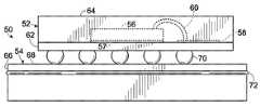
도 2는 예시적인 인쇄 회로 기판(Printed Circuit Board; PCB)(54)에 플립-장착된(flip-mounted) IC 패키지(52)를 포함하는 통신 디바이스(50)의 대표적인 측면도를 나타낸다. 이러한 예시에서, IC 패키지(52)는 다이(56), 접지 평면(57), 안테나(58), 다이와 안테나를 연결하는 결합 와이어(60)를 포함하는 결합 와이어들을 포함하는 것으로 나타내어질 수 있다. 다이, 안테나, 결합 와이어들은 패키지 기판(62) 상에 장착되고 캡슐화 물질(64) 내에 캡슐화된다. 접지 평면(57)은 다이(56)의 더 낮은 표면에 장착될 수 있고, 다이를 위한 전기적 접지를 제공하도록 구성된 여하한 적합한 구조일 수 있다. PCB(54)는 주요 면 또는 표면(68)을 갖는 상단 유전체 층(66)을 포함할 수 있다. IC 패키지(52)는 표면(68)에 금속배선 패턴(metallization pattern)(미도시)에 부착된 플립-마운팅 범프(flip-mounting bump)들로 플립-장착된다.2 illustrates an exemplary side view of a
PCB(54)는 PCB(54) 내에서 접지 평면을 형성하는 전도성 물질로 구성된 층(68)과 이격된 층(72)을 더 포함할 수 있다. PCB 접지 평면은 PCB(54) 상의 회로들 및 구성 요소들에게 전기적 접지를 제공하도록 구성되는 여하한 적합한 구조일 수 있다.The
도 3 및 도 4는 외부 회로 컨덕터들(84 및 86)을 갖는 IC 패키지(82)를 포함하는 또 다른 예시적인 통신 디바이스(80)를 나타낸다. 이러한 예시에서, IC 패키지(82)는 다이(88), 리드 프레임(90), 결합 와이어들의 형태의 전도성 커넥터들(92), 안테나(94), 캡슐화 물질(96) 및 도시를 간략하게 하기 위해 도시되지 않은 다른 구성 요소들을 포함할 수 있다. 다이(88)는 리드 프레임(90)으로 전기 통신 내에 장착될 수 있고, 리드 프레임(90)은 하나 이상의 다른 회로들을 다이(90)와 동작적으로 연결하는 것을 허용하도록 구성된 전기 컨덕터들 또는 리드들(98)의 여하한 적합한 배열일 수 있다. 안테나(94)는 리드 프레임(90)을 생산하는 제조 프로세스의 일부로서 구축될 수 있다.Figures 3 and 4 illustrate another
리드들(98)은, 패키지 기판(62)에 대응하는, 가상선들로 표시된 리드 프레임 기판(100)에 내장되거나 고정될 수 있다. 리드 프레임 기판은 리드들(98)을 소정의 배열로 충분히 고정하도록 구성된 여하한 적합한 절연체일 수 있다. 다이(88) 및 리드 프레임(90)의 리드들(98) 간의 전기적 통신은 전도성 커넥터들(92)를 사용하는 여하한 적합한 방법에 의해 달성될 수 있다. 언급된 것처럼, 전도성 커넥터들(92)은 다이(88)의 회로 상의 단자(terminal)들을 대응하는 리드 컨덕터들(98)과 전기적으로 연결하는 결합 와이어들을 포함할 수 있다. 예컨대, 컨덕터 또는 리드(98)는 리드 프레임 기판(100)의 상부 표면 상에 형성된 판금된 리드(plated lead)(102), 기판을 통해 연장하는 바이어(via)(104), IC 패키지(82)를 PCB와 같은 베이스 기판 상의 회로(미도시)에 장착하는 플립-마운팅 범프(106)를 포함할 수 있다. 베이스 기판 상의 회로는 외부 컨덕터(84)와 같은 외부 컨덕터들을 포함할 수 있고, 예컨대, 범프(106)를 베이스 기판을 통해 연장하는 추가적인 바이어(110)에 연결하는 스트립(strip) 컨덕터(108)를 포함할 수 있다. 다른 바이어들(112)은 리드 프레임 기판(100)을 통해 연장할 수 있고 베이스 기판을 통해 연장하는 추가적인 바이어들(114)이 존재할 수 있다.The leads 98 may be embedded or fixed in the
또 다른 예시에서, 다이(88)는 반전(invert)될 수 있고 전도성 커넥터들(92)은, 전술된 것처럼, 범프들, 또는 다이 솔더 볼(solder ball)들을 포함할 수 있고, 일반적으로 "플립 칩(filp chip)" 배열로서 알려진 것처럼 다이(88)의 회로 상의 포인트들을 대응하는 리드들(98)에 직접적으로 전기적으로 연결하도록 구성될 수 있다.In another example, the die 88 can be inverted and the conductive connectors 92 can include bumps, or die solder balls, as described above, May be configured to electrically connect the points on the circuitry of the die 88 directly to corresponding leads 98 as known as a " chip "chip arrangement.
제1 및 제2 IC 패키지(10)는 하나의 PCB 상에 함께 위치될 수 있고 인트라-PCB(intra-PCB) 통신을 제공할 수 있다. 다른 예시들에서, 제1 IC 패키지(10)는 제1 PCB 상에 위치될 수 있고 제2 IC 패키지(10)는 제2 PCB 상에 위치될 수 있고 따라서, 인트라-PCB 통신을 제공할 수 있다.The first and second IC packages 10 can be co-located on one PCB and can provide intra-PCB (intra-PCB) communication. In other examples, the
도 5 및 6으로 돌아와서, 예시적인 휴대용 디바이스가 설명될 것이다. 휴대용 디바이스(120)는 유도 파워 시스템을 사용하여 무선으로 파워를 제공받고 또한 하나 이상의 IC 패키지들(10)을 사용하여 무선으로 통신하도록 구성된 여하한 디바이스일 수 있다. 휴대용 디바이스(120)는 EHF 통신 회로(122), 데이터 스토리지 유닛(124), 로컬 파워 스토리지 디바이스(126) 및/또는 유도 파워 수신기(128)을 포함할 수 있다. 휴대용 디바이스(120)의 구성 요소들은 케이스(미도시) 내에 포함될 수 있다. 도 5 및 6은 다양한 구성 요소들의 가능한 위치들을 보여주는 휴대용 디바이스(120)의 예시를 묘사한다. 도 6은 도 5 내에 도시된 디바이스의 부분적인 분해된 버전이다. 휴대용 디바이스는 휴대용 매체 디바이스(Portable Media device; PMD)일 수 있고, 휴대폰, 개인 휴대 정보 단말기(Personal Digital Assistant; PDA), MP3 플레이어들, 노트북 컴퓨터, 또는 태블릿의 형태를 취할 수 있다.Returning to Figures 5 and 6, an exemplary handheld device will be described. The
EHF 통신 회로(122)는 하나 이상의 IC 패키지들(10)을 사용하여 무선으로 통신하도록 구성된 여하한 회로일 수 있다. 예컨대, EHF 통신 회로(122)는 2개의 IC 패키지들(130 및 132)를 포함할 수 있고, 도 5 및 6에서 묘사된 것처럼 하나는 송신기로서 구성되고 나머지는 수신기로서 구성될 수 있다. IC 패키지들(130 및 132)는 동일한 디바이스 내의 다른 이러한 칩들 보다는 다른 디바이스들 내의 다른 IC 패키지들과 통신하도록 구성될 수 있다. 몇몇의 예시들에서, 송신기로서 구성된 IC 패키지로, 단지 하나의 IC 패키지가 포함될 수 있다.The
EHF 통신 회로(122)는 디지털 데이터 스토리지 유닛(124)과 전기 통신 내에 있을 수 있다. 데이터 스토리지 유닛(124)은 데이터를 독출 및 기입하는 것이 가능한 여하한 적절한 데이터 스토리지 유닛일 수 있다. 예컨대, 데이터 스토리지 유닛(124)은 IC 칩, 카드, 디스크 또는 솔리드 스테이트 드라이브(Solid State Drive; SSD)일 수 있다. 전형적인 동작에서, EHF 통신 회로(122)는 데이터 스토리지 유닛(124) 및 외부 디바이스 간에 데이터를 전송할 수 있다.The
EHF 통신 유닛(122)는 또한 로컬 파워 스토리지 디바이스(126)로부터 파워를 수신할 수 있다. 파워 스토리지 디바이스(126)는 장래의 사용을 위한 전기 에너지를 저장하도록 구성된 여하한 적절한 디바이스일 수 있다. 예컨대, 파워 스토리지 디바이스(126)는 리튬 이온 배터리, 연료 전지, 울트라캐패시터, 또는 여하한 다른 충전 및 방전될 수 있는 배터리-유사 디바이스일 수 있다. 전형적으로, 이러한 디바이스에 의해 공급되는 전압은 회로 및 IC 패키지들에 의해 사용 가능한 전압으로 만들기 위해 EHF 통신 회로(122) 내의 적절한 회로망을 사용하여 스텝 다운(stepped down)될 필요가 있을 수 있다. IC 패키지(130 및 132)와 같은 IC 패키지들은 대략 1.2 내지 3.3V의 범위 내에서 동작한다.The
유도 파워 수신기(128)는 로컬 파워 스토리지 디바이스(126)와 전기 통신 내에 있을 수 있고 파워 스토리지 디바이스(126)를 충전하기 위해 기능할 수 있다. 유도 파워 수신기(128)는 파워 소스로부터의 무선 에너지 전송을 수신하는 것이 가능한 여하한 적절한 디바이스일 수 있다. 예컨대, 유도 파워 수신기(128)는 분리된 충전 디바이스 내에 배치된 1차 코일에 의해 전류가 유도되는 2차 코일(129)을 포함할 수 있다. 이러한 유도 충전의 일종에 대한 세계적인 개방 표준들이 개발되고 있다. 예컨대, 무선 파워 컨소시움(Wireless Power Consortium)에 의해 개발된 "Qi" 표준은 상업적인 상품들 내에서 활용되기 시작했다.The
도 5 및 6에서 도시된 휴대용 디바이스(120)는 전도성 서프레서(134), 유전체 절연 배리어(136), 및 유전체 지시 부분(138)을 더 포함할 수 있다. 전도성 서프레서(134)는 기생(spurious) EHF 방사의 진입 또는 방출(ingress or egress)을 억제하도록 구성되는 여하한 적절한 구조일 수 있다. 예컨대 서프레서(134)는 유전체 절연 배리어(136) 주위에 횡방향으로 배치된 전도성 물질의 확장으로서 구축될 수 있다. 유전체 절연 배리어(136)는 서프레서(134)로부터 유전체 지시 부분(138)을 절연하도록 구성된 여하한 적합한 구조 또는 틈일 수 있다. 예컨대, 유전체 절연 배리어(136)는 거품과 같은 낮은-Er 유전체일 수 있고 또는 유전체 지시 부분(138)을 횡방향으로 둘러싸는 공기 틈일 수 있다. 유전체 지시 부분(138)은 EHF 방사를 향상 및/또는 지시하도록 구성된 여하한 적절한 유전체 구조일 수 있다. 예컨대, 유전체 지시 부분(138)은 플라스틱과 같은 높은-Er 물질의 블록일 수 있다.The
휴대용 디바이스(120)과 같은 휴대용 디바이스는 독립적으로 기능할 수 있고(예컨대, 휴대용 미디어 디바이스처럼), 상호작용 및/또는 다른 디바이스들로부터 파워를 수신할 수 있다. 예컨대, 베이스 유닛은 하나의 이러한 디바이스일 수 있다. 도 7 및 8에서처럼, 베이스 유닛(140)은 휴대용 디바이스(120)와 무선으로 통신하도고 휴대용 디바이스(120)로 무선으로 파워를 공급하도록 구성된 여하한 적절한 디바이스일 수 있다. 예컨대, 베이스 유닛(140)은 유도 파워 소스(142) 및/또는 EHF 통신 회로(144)를 둘러싸는(enclose) 하우징(미도시)를 포함할 수 있다.A portable device, such as the
몇몇의 예시들에서, 베이스 유닛(140)은 호스트 컨트롤러(미도시)를 포함하거나 호스트 컨트롤러와 통신할 수 있고, 호스트 컨트롤러는 휴대용 디바이스(120) 및 베이스 유닛(140)을 포함하는 전체 시스템의 전자적인 활동을 제어하도록 구성된 여하한 적절한 디바이스 또는 구성 요소일 수 있다. 예컨대, 호스트 컨트롤러는 소프트웨어 및/또는 펌웨어를 통해 휴대용 디바이스(120) 및 퍼스널 컴퓨터 간의 데이터의 동기화를 조정(coordinate)하도록 구성된 퍼스널 컴퓨팅 디바이스일 수 있다. 다른 예시들에서, 호스트 컨트롤러는 비디오 플레이어; 오디오 플레이어; 보안 시스템; 디스플레이 시스템; 음악, 비디오 및/또는 오디오북 제작기(organizeer); 데이터 백업 스토리지 시스템; 휴대 전화 매니저 등 중 하나 또는 모두를 포함할 수 있다.In some instances, the
몇몇의 실시예들에서, 2개의 디바이스들의 적어도 몇몇의 역할들은 서로 바뀔 수 있음에 유의한다. 따라서, 호스트 컨트롤러는 휴대용 디바이스(120) 내에 배치될 수 있고 베이스 유닛(140)은 스토리지 유닛(124)와 같은 스토리지 유닛을 포함할 수 있다. 다른 예시들에서, 디바이스들 양자는, 디바이스-투-디바이스(device-to-device) 데이터 복사와 같은 기능성을 가능하게 하는, 호스트 컨트롤러 및/또는 스토리지 유닛(12)를 포함할 수 있다. 다른 실시예들에서, 휴대용 디바이스(120)는 작업(transaction)을 제어할 수 있고 그로 인해 휴대용 디바이스(120) 상에서 재생 또는 가용한 비디오가 비디오 디스플레이를 포함하는 베이스 유닛(140) 상에 나타날 수 있다. 이러한 작업은 휴대용 기기로부터 전체적으로 제어될 수 있다.It is noted that in some embodiments, at least some of the roles of the two devices may be interchanged. Thus, the host controller may be located within the
유도 파워 소스(142)는 유도 파워 수신기(128)에 무선으로 전기 파워를 제공하도록 구성된 여하한 적절한 디바이스일 수 있다. 전술된 것처럼, 유도 파워 소스(142)는 1차 코일(146)을 포함할 수 있다.The
EHF 통신 회로(144)는, 휴대용 디바이스(120) 내에서 IC 패키지(들)로 및 IC 패키지(들)로부터 정보를 전송하도록 구성된, IC 패키지들(148 및 150)과 같은, 하나 이상의 IC 패키지들(10)을 포함할 수 있다. 휴대용 디바이스(120) 내의 각 송신기 IC 패키지에 대해, 대응하는 수신기 IC 패키지는 베이스 유닛(140) 내에서 제공될 수 있다. 유사한 방식(similar fashion)으로, 휴대용 디바이스(120) 내의 수신기는 베이스 유닛(140) 내에 대응하는 송신기를 가질 수 있다. 몇몇의 예시들에서, IC 패키지들은 송수신기(transceiver)들로서 구성될 수 있고, 디바이스 당 하나의 IC 패키지를 사용하여 각각 양-방향 링크가 마련될(established) 수 있다. 데이터 전송을 용이하게 하기 위해, 결과적인 송신기-수신기 또는 송수신기-송수신기 쌍들은 적절한 일반적인 디바이스들의 정렬이 또한 IC 패키지들의 모든 쌍들을 정렬하도록 배치될 수 있다.
대안적으로, 몇몇의 송신기-수신기 또는 송수신기-송수신기 쌍들은 디바이스들이 제1 구성 내에 배치될 때 정렬될 수 있고, 다른 것들은 디바이스들이 제2 구성 내에 배치될 때 정렬될 수 있다. 예컨대, 베이스 유닛(140)는 인터페이스 표면 상에 마킹들의 2개의 세트들을 제공할 수 있다. 마킹들의 한 세트는 휴대용 디바이스(120)가 데이터 동기화를 가능하게 하기 위해 배치될 곳을 지시할 수 있고, 나머지는 휴대용 디바이스(120)가 음악 재생 또는 몇몇의 다른 기능성들을 가능하게 하기 위해 배치될 곳을 지시할 수 있으며, 양자의 위치들은 배터리 충전을 동시에 허용할 수 있다.Alternatively, some of the transmitter-receiver or transceiver-transceiver pairs may be aligned when the devices are placed in the first configuration, and others may be aligned when the devices are placed in the second configuration. For example, the
도 7 및 도 8은 휴대용 디바이스(120) 및 베이스 유닛(140)을 나타낸다. 도 7에서 묘사된 것처럼, 유도 파워 소스(142) 및 IC 패키지들(148 및 150)은 휴대용 디바이스(120) 내의 대응하는 구성 요소들을 보완하는 공간적 배열 내에서 배치 및 구성될 수 있다. 도 8은 이러한 보완적인 배열을 도시하고, 베이스 유닛(140)에 도킹 정렬(docking alignment)되는 휴대용 디바이스(120)를 묘사한다. 앞서 언급된 것처럼, 각 디바이스는 송신기 및 수신기로서 각각 구성된 2개의 IC 패키지들 보다는 송수신기로서 구성된 단일한 IC 패키지를 포함할 수 있다.Figs. 7 and 8 show the
휴대용 디바이스(120) 및 베이스 유닛(140)과 같은 디바이스들 간에 전송 및 수신될 수 있는 EHF 신호들에 대해, 주어진 면허권 있는 방출 대역(licensed emissions band)에 대한 정부의 방출 제한(governmental emissions limit)들이 존재할 수 있다. 변조되지 않은 신호는 방출의 더 좁은 대역을 제공할 수 있고, 이로 인해 몇몇의 어플리케이션들 내에서 방출 제한의 위반을 회피할 수 있음에 유의한다. 한편, 변조된 신호는 몇몇의 어플리케이션들 내에서 면허권 있는 대역 외부에서 연장할 수 있는 방출의 더 넓은 대역을 제공할 수 있다.For EHF signals that can be transmitted and received between devices such as the
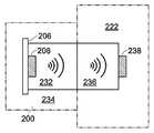
도 9 및 도 10은 주어진 대역의 외부에서 연장할 수 있는 방출의 생성을 제한하도록 구성된 2개의 예시적인 디바이스들을 나타내는 블록도이다. 제1 전자 디바이스(160)의 일부는 IC 패키지들(10)의 2개의 예시들, 베이스밴드 변조 회로(169)에 전기적으로 연결된, 특히 송신기(162) 및 수신기(164)를 포함할 수 있다. 불연속 쉴드(168)는 IC 패키지들(162 및 164)를 부분적으로 둘러쌀 수 있다. 예컨대, 제1 전자 디바이스(160)의 일부는 EHF 신호들을 억제(inhibit) 또는 차단하도록 동작하는 물질의 층 또는 섹션(section)을 포함할 수 있다. 쉴드(168)는 EHF 주파수를 갖는 전자기 신호들을 억제 또는 차단하도록 구성된 여하한 적절한 물질을 포함할 수 있다. 예컨대, 접지된 전자기적으로 전도성 있는 물질은 EHF 신호를 접지로 드레인(drain)할 수 있고 소산(dissipative)하는 물질은 EHF 신호를 흡수하고 이를 물질 내에서 열로 변환할 수 있다. 이러한 쉴딩 층 또는 섹션은 모든 방향에서 연속적인 쉴드를 형성하지 않는 다는 점에서 불연속일 수 있고, 하나 이상의 방향들에서 오히려 개구부 또는 개구부들을 포함한다. 부분적인 쉴딩 구성은 U-형태의 단면으로서 도 9 및 10에서 나타내어진다. 하기에서 더 설명되는 것처럼, 쉴드(168)은 또 다른 디바이스 상의 대응하는 쉴드와의 메이팅 관계를 용이하게 하도록 구성될 수 있다.Figures 9 and 10 are block diagrams illustrating two exemplary devices configured to limit the generation of emissions that can extend outside of a given band. A portion of the first
송신기 칩(162)은 전술된 IC 패키지(10)의 예시일 수 있고, 베이스밴드 변조 회로(169)와 함께 상위 시리즈들(upstream series) 내의 디바이스(160) 내의 하나 이상의 회로들에 의해 제공되는 EHF 신호를 전송하기 위해 적합화될 수 있다. 예컨대, 송신기 칩(162)은 충분히 일정한 신호, 변조된 신호, 단속적인 신호, 이들의 조합, 또는 EHF 대역 내에서 전송 가능한 여하한 다른 신호를 전송할 수 있다. 리시버 칩(164)은 또한 이전에 설명된 IC 패키지(10)의 예시일 수 있고, EHF 신호를 수신하고 전자적 형태의 그 신호를 제1 디바이스(160) 내의 베이스밴드 변조 회로(169)를 포함하는 하나 이상의 회로들로 제공하기 위해 적합화될 수 있다. 송신기 및 수신기 패키지들(162 및 164)은 몇몇의 예시들 내에서 전송 및 수신의 양자를 수행하도록 구성된 단일한 송수신기 패키지에 의해 교체될 수 있다.The
베이스밴드 변조 회로(169)는 하나 이상의 입력들에 기반하여 둘 이상의 신호들 간을 선택하도록 구성된 여하한 적절한 회로일 수 있다. 도 9 및 10에 도시된 실시예에서, 베이스밴드 변조 회로(169)는 송신기 칩(162), 수신기 칩(164), 변조된 신호 생성기, 및 변조되지 않은 신호 생성기와 같은 하나 이상의 신호 생성 회로들로부터 입력들을 수신하기 위해 적합화된 멀티플렉서 회로를 포함할 수 있다.The
도 9 및 10을 계속하여 참조하면, 제2 전자 디바이스(176)은 제1 디바이스(160)과 유사할 수 있고, 제1 디바이스(160)의 대응하는 구성 요소들과 유사한 기능들 및 연결들을 갖는 송신기 칩(178), 수신기 칩(180), 베이스밴드 변조 회로(185) 및 쉴드(184)를 포함할 수 있다.9 and 10, the second
도 9 및 10에서 묘사된 것처럼, 디바이스들(160 및 176)은 미정렬 상태에서 정렬된 관계로 물리적으로 이동될 수 있다. 이러한 맥락에서, 정렬은 송신기-수신기 쌍들의, 즉 송신기(178) 및 수신기(164)뿐만 아니라, 즉, 송신기(162) 및 수신기(180)의 축상의 및 근위(axial and proximal)의 정렬을 참조한다. 다른 예시들에서, 이들은 적절한 송수신기-송수신기 쌍에 의해 교체될 수 있다. 이러한 쌍들의 적절한 정렬은 적어도 하나의 쌍들 간의 EHF 신호 통신 및 따라서 제1 및 제2 디바이스들 간의 통신을 허용할 수 있다. 디바이스들(160 및 176)의 쉴드들은 또한 송신기-수신기 또는 송수신기-송수신기 쌍들이 적절한 정렬 내에 있을 때 쉴드들이 정렬되는 것을 보장하도록 구성될 수 있다. 이전에 언급된 것처럼, 불연속 쉴드(168) 및 불연속 쉴드(184)는 메이트들로서 구성될 수 있고, 쉴드들이 정열된 및 메이트된 위치 내에 배치될 때 IC 패키지들의 쌍들 주위에서 단일한 연속적인 쉴드를 형성하는 것이 가능하다.As depicted in Figures 9 and 10,
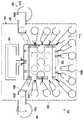
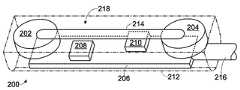
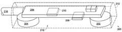
이제 도 11 및 12로 돌아가서, 하나 이상의 IC 패키지들을 포함하는(incorporating) 예시적인 커넥터(200)가 묘사된다. 커넥터(200)는 또 다른 디바이스 또는 시스템 상의 대응하는 커넥터 부품에 대한 영 또는 낮은-삽입 EHF 연결 인터페이스를 제공하도록 구성된 여하한 적합한 커넥터 부품일 수 있다. 커넥터(200)는 2개의 자석들(202 및 204), 커넥터 PCB(206), 208 및 210으로서 라벨된 2개의 IC 패키지들(10), 커넥터 바디(212) 및/또는 커넥터 정렬 부분(214)를 포함할 수 있다. 또한, 커넥터(200)는 전기적으로 및 물리적으로 케이블(216)에 연결될 수 있다.Turning now to Figures 11 and 12, an
커넥터 바디(212)는 커넥터(200)의 다른 구성 요소들을 위한 하우징 또는 컨테이너로서 역할할 수 있다. 몇몇의 예시들에서, 커넥터 바디(212)는 적절한 유전체 물질 또는 물질들을 사용하여 PCB(206) 및 IC 패키지들(208 및 210)을 캡슐화할 수 있다. 커넥터 바디(212)는 또한 사용자에 의한 편리한 조작을 허용하도록 크기가 결정되고 구성될 수 있다. 자석들(202 및 204)는 적어도 부분적으로 커넥터 바디(212) 내에 보관될 수 있고, 자석들 양자가 커넥터 바디(212)의 메이팅 표면(218)과 충분히 같은 높이(flush with)가 되도록 장착될 수 있다.The
메이팅 표면(218)은 적절한 물리적 커플링 표면에 대응하는 디바이스 상의 대응하는 커넥터를 제공하도록 구성될 수 있다. 몇몇의 예시들에서, 메이팅 표면(218)은 평면이다. 다른 예시들에서, 메이팅 표면(218)은 굽어진다(curved). 또 다른 예시들에서, 메이팅 표면(218)은 정렬 부분(214)를 포함할 수 있다. 정렬 부분(214)은 도 13에 도시된 것처럼, 사용자에게 물리적인 정렬 피드백을 제공하게 위한, 돌출부(protrusion), 릿지(ridge), 노브(knob), 베벨(bevel), 핀(pin), 함몰부(recess) 또는 외부 디바이스(222)의 대응하는 목표 연결 영역(220) 상의 대응하는 부분에 메이팅하도록 구성된 다른 멤버(member)일 수 있다.The
자석들(202 및 204)은 커넥터(200)를 릴리즈 가능하게 근접하게 정렬된 외부 디바이스(222)의 목표 연결 영역(220)에 고정하도록 구성된 여하한 자기 구성 요소들일 수 있다. 이러한 맥락에서, 정렬 및 근접은, 충분히 정렬될 필요가 있고 주어진 패키지들의 쌍 간의 통신이 가능하도록 충분히 가까울 필요가 있는, IC 패키지들의 정렬 및 근접을 참조할 수 있다. 몇몇의 예시들에서, 자석들(202 및 204)는 영구 자석들 이다. 다른 예시들에서, 자석들(202 및 204)은 전자석들이다. 또 다른 예시들에서, 자석들(202 및 204)은 목표 연결 영역(220) 상의 또는 인근의 자석들을 자기적으로 끌어당기는 것이 가능한 철금속(ferrous material)으로 구축된다.The
IC 패키지들(208 및 210)은 커넥터 PCB(206) 상에 장착될 수 있다. 몇몇의 예시들에서, 더 많은 또는 더 적은 패키지들, 어셈블리들, 또는 칩들이 제공될 수 있다. IC 패키지들(208 및 210)은 IC 패키지(208)의 안테나가 IC 패키지(210)의 안테나에 대해 직교하도록 향하여, 편극 효과들을 활용할 수 있도록 PCB(206) 상에 장착될 수 있다. 다시 말해, 직교하는 방향은 직교하는 EHF 신호들이 서로 충분히 간섭하지 않을 것이기 때문에 패키지들이 서로 가깝게 장착되는 것을 허용할 수 있다.The IC packages 208 and 210 may be mounted on the
커넥터 PCB(206) 및 관련된 회로들은 커넥터(200)가 커넥터(200)의 외부의 소스로부터 파워 및/또는 정보의 신호들을 획득하는 것을 허용하도록 케이블(216)에 전기적으로 연결될 수 있다. 예컨대, 케이블(216)은 커넥터(200)에게 퍼스널 컴퓨터 또는 다른 호스트 디바이스로 및/또는 퍼스널 컴퓨터 또는 다른 호스트 디바이스로부터의 데이터 신호 경로를 제공할 뿐만 아니라 전기적 파워를 제공할 수 있다.The
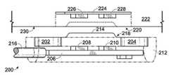
도 13은 도시된 외부 디바이스(222)에 근접하는 커넥터(220)를 나타낸다. 도 13에서 묘사된 것처럼, 외부 디바이스(222)는 2개의 외부 디바이스의 에지(230) 인근에 배치된 IC 패키지들(226 및 228)을 갖는 외부 디바이스 PCB(224)를 포함할 수 있다. 몇몇의 예시들에서, 각각 하나 이상의 칩들을 포함하는, 더 많은 또는 더 적은 IC 패키지들이 제공될 수 있다. 에지(230)에서 목표 연결 영역(220)은 자석들(202 및 204)이 부착하는 자기적으로 끌어당기는 표면을 제공하는 철금속 또는 여하한 다른 물질로 구성된 부분들을 포함할 수 있다. 예컨대, 커넥터(200)를 외부 디바이스(220)의 목표 연결 영역(220) 인근에 배치하는 것은 자석들(202 및 204)이 목표 연결 영역(220)에 끌어당겨지는 것을 야기하고, 커넥터(200)를 IC 패키지들(208 및 210)이 IC 패키지들(226 및 228)과 정렬하고 통신하도록 허용하는 적절한 위치 및 정렬로 당길 수 있다.13 shows a
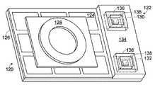
도 14에 묘사된 것처럼, 커넥터 바디(212)는 IC 패키지(208 및/또는 210)(편의를 위해 도 14에서는 IC 패키지(208)로서 도시됨)의 적어도 일부를 둘러싸는 제1 유전체 물질(232) 및 제1 유전체 물질(232)의 적어도 일부를 둘러싸는 제2 유전체 물질(234)를 포함할 수 있다. 제1 유전체 물질(232)은 제2 유전체 물질(234)에 비해 상대적으로 높은 유전률을 가질 수 있다. 예컨대, 유전체 물질(232)은 대략 2 내지 대략 5의 유전률을 갖는 플라스틱을 포함할 수 있고, 유전체 물질(234)은 상대적으로 더 낮은 유전률을 갖는 물질(substance)을 포함할 수 있다. 몇몇의 예시들에서, 유전체 물질(234)은 거품 또는 공기 틈을 포함할 수 있다.14, the
제1 유전체 물질(232)은 IC 패키지(208)로부터 커넥터(200)의 메이팅 표면(218)의 영역에 미치는(spanning) 물질의 체적(volume)으로서 구성될 수 있다. 더 낮은 유전율 물질에 의해 둘러싸인 더 높은 유전율 물질을 포함하는, 이러한 구조는 유전체 물질(232)을 통해 전송된 EHF 신호의 집중(focusing) 및 쉐이핑(shaping)을 용이하게 할 수 있다. 몇몇의 예시들에서, 대응하는 높은-유전체 물질(236)은 외부 디바이스(222)의 표면에서 목표 연결 영역(220)으로부터 하나 이상의 IC 패키지들(238)에 미치는 외부 디바이스 내에 포함될 수 있다. 이러한 예시에서, 목표 연결 영역(220)에 근접하는 정렬 커넥터(200)는 EHF 신호가 패키지(208)로부터 패키지(238)로 통해서 전파할 수 있는 충분히 연속적인 유전체 물질의 경로를 생성한다.The first
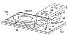
도 15 및 16은 커넥터(250)의 2개의 뷰들을 묘사하고, 이는 도 9 및 10에 대해 설명된 것과 유사한 부분적인 쉴딩을 포함하는 커넥터(200)의 예시일 수 있다. 도 16은 도 15 내의 선 16-16을 따라 취해진 횡단면을 나타낸다.. 커넥터(200)과 유사하게, 커넥터(250)는 2개의 자석들(252 및 254), PCB(256), 2개의 IC 패키지들(258 및 260), 및 바디(262)를 포함할 수 있고, 포함된 제1 유전체 물질(264)은 IC 패키지들에 근접하고 제1 유전체 물질(264)을 둘러싸는 제2 유전체 물질(266)은 더 낮은 유전율을 갖는다.Figures 15 and 16 depict two views of the
이러한 예시에서, 쉐이딩 물질(268)은 커넥터 바디(262)의 적어도 일부 내에서 제공될 수 있다. 쉐이딩 물질(268)은 들어오는 및 나가는 기생 EHF 방사를 흡수하거나 아니면 차단하도록 구성된 여하한 소산하는 또는 전기적으로 전도성 있는 물질 또는 레이어를 포함할 수 있다. 예컨대, 쉐이딩 물질(268)은 IC 패키지들 주위를 감싸고 메이팅 표면(270)의 적어도 일부는 남겨두는 구리 시트 또는 레이어를 포함할 수 있다. EHF 방사에 대해 흡수 및/또는 소산하는 쉴드로서 동작함에 더하여, 쉴딩 물질(268)은 커넥터(250) 내의 하나 이상의 회로들을 위한 전기 회로 접지를 제공할 수 있다.In this example, the
도 17은 전술된 구성 요소들의 몇몇을 포함하는 예시적인 어댑터(280)의 측단면 뷰를 묘사하는 간략화된 다이어그램이다. 어댑터(280)는 IC 패키지-가능 외부 디바이스(282)를 표준 기계적인 또는 물리적인 플러그-타입 커넥터와 함께 사용하기 위해 적합화하도록 구성된 여하한 적절한 시스템일 수 있다. 어댑터(280)는 어댑터 슬리브(284), 암(female) 커넥터 소자(286), IC 패키지(288), 및 유전체 및 쉴딩 구조(290)를 포함할 수 있다.17 is a simplified diagram depicting a side sectional view of an
어댑터 슬리브(284)는 어댑터를 위한 하우징일 수 있고 또한 외부 디바이스(282)의 적어도 일부 주위에서 밀접하게 꼭 맞을(fit) 수 있고, 외부 디바이스의 IC 패키지(292)를 IC 패키지(288)에 정렬한다. 예컨대, 어댑터 슬리브(284)는 디바이스를 위한 부분적인 케이스로서 구성될 수 있다. IC 패키지(288)는 슬리브(284)가 디바이스(282)에 부착될 때 외부 디바이스 내에서 IC 패키지(292)와 정렬 및 통신할 수 있다. IC 패키지(288)는 또한 암 커넥터 소자(286)와 전기 통신 내에 있을 수 있다. 암 커넥터 소자(286)는 물리적인 플러그-타입 커넥터의 대응하는 수(male) 커넥터 소자(294)에 대한 표준 플러그-인 커넥터 인터페이스를 나타낼 수 있다.The
IC 패키지(288)는 전술된 구조들과 유사한 유전체 및 쉴딩 구조(290)에 내장되거나 또는 유전체 및 쉴딩 구조(290)에 의해 둘러싸여질 수 있다. 구조(290)는 도 17에 묘사된 것처럼, 쉴딩 물질 또는 레이어(300) 뿐만 아니라 IC 패키지(288)를 둘러싸는 높은-유전률 물질(296), 낮은-유전률 물질(298)에 의해 부분적으로 둘러싸이는 물질(296)을 포함할 수 있다. IC 패키지들(288 및 292) 간의 EHF 신호의 통신은 구조(290)에 의해 용이해질 수 있다. 전술된 것처럼, 신호는 또한 암 커넥터 소자(286)를 통해 IC 패키지(288) 및 수 커넥터 소자(294) 간에 통신될 수 있다. 따라서, 어댑터(280)는 물리적인 커넥터 시스템 및 IC 패키지-가능, 물리적-커넥터리스(connectorless) 외부 디바이스(282) 간을 적합화할 수 있다.The
따라서, 무선 파워 및 데이터 전송을 제공하기 위한 전술된 시스템, 디바이스, 또는 방법은 하나 이상의 하기의 예시들을 포함할 수 있다.Thus, the above-described system, device, or method for providing wireless power and data transmission may include one or more of the following examples.
제1 실시예에서, 전자 디바이스는 제1 유전체 기판, 기판에 의해 지지되는 데이터를 처리하기 위한 적어도 하나의 제1 전자 회로, 및 제1 안테나를 포함하는 적어도 하나의 제1 통신 유닛을 포함할 수 있다. 제1 통신 유닛은 디지털 정보를 포함하는 제1 EHF 전자기 신호 및 적어도 하나의 제1 전자 회로에 의해 컨덕트되는 제1 데이터 신호 간의 변환(converting)을 위해 적어도 하나의 제1 전자 회로와 통신하며 기판에 장착될 수 있다. 제1 전자기 신호는 제1 안테나에 의해 제1 신호 경로를 따라 전송 또는 수신될 수 있다. 제1 전자기(ElectroMagnetic; EM)) 신호 가이드(guide) 어셈블리는 제1 신호 경로 내에서 제1 안테나에 근접하게 배치된 제1 유전체 물질로 구성된 제1 유전체 소자를 포함할 수 있다. 제1 EM 신호 가이드는 제1 신호 경로를 따라 연장하는 측면들(sides)을 포함할 수 있다. 제1 슬리브 소자는 제1 유전체 소자의 측면들의 적어도 일부분을 따라 제1 유전체 소자 주위에서 연장할 수 있다. 제1 슬리브 소자는 제1 유전체 소자의 측면들을 통한 제1 전자기 신호의 전송을 저해할 수 있다.In a first embodiment, an electronic device may comprise a first dielectric substrate, at least one first electronic circuit for processing data supported by the substrate, and at least one first communication unit comprising a first antenna have. The first communication unit communicates with at least one first electronic circuit for converting between a first EHF electromagnetic signal comprising digital information and a first data signal conducted by at least one first electronic circuit, As shown in FIG. The first electromagnetic signal may be transmitted or received along the first signal path by the first antenna. A first electromagnetic (EM)) signal guide assembly may include a first dielectric element comprised of a first dielectric material disposed proximate to a first antenna within a first signal path. The first EM signal guide may include sides extending along the first signal path. The first sleeve element may extend around the first dielectric element along at least a portion of the sides of the first dielectric element. The first sleeve element may impede transmission of the first electromagnetic signal through the sides of the first dielectric element.
제1 슬리브 소자는 전기적으로 전도성 있는 물질(electrically conductive material), 전자기적으로 흡수성 있는 물질(electromagnetically absorptive material), 전자기적으로 소산하는 물질(electromagnetically dissipative material) 및 제1 유전체 소자의 유전율보다 더 낮은 유전율을 갖는 제2 유전체 물질 중 하나로 구성될 수 있다.The first sleeve element may comprise an electrically conductive material, an electromagnetically absorptive material, an electromagnetically dissipative material, and a dielectric constant lower than the dielectric constant of the first dielectric element. And a second dielectric material having a second dielectric material.
제1 슬리브 소자는 제2 유전체 물질로 구성되고 제1 유전체 소자의 측면들에 대응하는 상기 신호 경로를 따라 연장하는 측면들을 포함할 수 있다. 신호 가이드는 제1 슬리브 소자의 측면들 주위에 배치되는 제2 슬리브 소자를 포함할 수 있고, 전자기적으로 소산하는 물질로 구성될 수 있다.The first sleeve element may comprise side surfaces that are comprised of a second dielectric material and that extend along the signal path corresponding to the sides of the first dielectric element. The signal guide may include a second sleeve element disposed about the sides of the first sleeve element and may be constructed of a material that dissipates electronically.
제1 통신 유닛은 송수신기일 수 있다.The first communication unit may be a transceiver.
적어도 하나의 제1 통신 유닛은 제2 안테나를 포함하는 제2 통신 유닛을 포함할 수 있다. 제2 통신 유닛은 디지털 정보를 포함하는 제2 EHF 전자기 신호 및 적어도 하나의 제1 전자 회로에 의해 컨덕트되는 제2 데이터 신호 간의 변환을 위해 적어도 하나의 제1 전자 회로와 통신하며 기판에 장착될 수 있다. 제2 전자기 신호는 제2 안테나에 의해 제2 신호 경로를 따라 전송 또는 수신될 수 있다. 전자기 신호 가이드 어셈블리는 제2 신호 경로 내에서 제2 안테나에 근접하게 배치된 제3 유전체 물질로 구성되고 제2 신호 경로를 따라 연장하는 측면들을 포함하는 제2 유전체 소자를 포함할 수 있다. 제2 슬리브 소자는 제2 유전체 소자의 측면들의 적어도 일부분을 따라 제2 유전체 소자 주위에서 연장할 수 있다. 제2 슬리브 소자는 제2 유전체 소자의 측면들을 통한 제2 전자기 신호의 전송을 저해할 수 있다.The at least one first communication unit may comprise a second communication unit comprising a second antenna. The second communication unit communicates with at least one first electronic circuit for conversion between a second EHF electromagnetic signal comprising digital information and a second data signal conducted by at least one first electronic circuit, . The second electromagnetic signal may be transmitted or received along a second signal path by a second antenna. The electromagnetic signal guide assembly may comprise a second dielectric element comprised of a third dielectric material disposed proximate to the second antenna within the second signal path and including sides extending along the second signal path. The second sleeve element may extend around the second dielectric element along at least a portion of the sides of the second dielectric element. The second sleeve element may impede the transmission of the second electromagnetic signal through the sides of the second dielectric element.
제2 슬리브 소자는 제2 유전체 소자의 유전율보다 더 낮은 유전율을 갖는 제4 유전체 물질로 구성될 수 있다. 제2 슬리브 소자는 제2 유전체 소자의 측면들에 대응하는 제2 신호 경로를 따라 연장하는 측면들을 포함할 수 있다. 신호 가이드 어셈블리는, 제1 및 제2 슬리브 소자들 간을 연속적으로 연장하고, 전기적으로 전도성 있는 물질로 구성된, 제1 및 제2 슬리브 소자들의 측면들 주위에 배치된 슬리브 어셈블리를 더 포함할 수 있다.The second sleeve element may be comprised of a fourth dielectric material having a lower dielectric constant than the dielectric constant of the second dielectric element. The second sleeve element may include sides extending along a second signal path corresponding to the sides of the second dielectric element. The signal guide assembly may further include a sleeve assembly that extends continuously between the first and second sleeve elements and is disposed about the sides of the first and second sleeve elements, the sleeve assembly being comprised of an electrically conductive material .
제1 통신 유닛은 송신기이고, 제2 통신 유닛은 수신기일 수 있다.The first communication unit may be a transmitter and the second communication unit may be a receiver.
전자 시스템은 제1 전자 디바이스 및 제2 유전체 기판, 제2 기판에 의해 지지되는 데이터를 처리하기 위한 적어도 하나의 제2 전자 회로 및 제2 안테나를 포함하는 적어도 하나의 제2 통신 유닛을 포함하는 제2 전자 디바이스를 포함할 수 있다. 제2 통신 유닛은 디지털 정보를 포함하는 제2 EHF EM 신호 및 적어도 하나의 제2 전자 회로에 의해 컨덕트되는 제2 데이터 신호 간의 변환을 위해 적어도 하나의 제2 전자 회로와 통신하며 제2 기판에 장착될 수 있다. 제2 전자기 신호는 제2 안테나에 의해 제2 신호 경로를 따라 전송 또는 수신될 수 있다. 제2 EM 신호 가이드 어셈블리는 제2 신호 경로 내에서 제2 안테나에 근접하게 배치된 제2 유전체 물질로 구성되고 제2 신호 경로를 따라 연장하는 측면들을 포함하는 제2 유전체 소자를 포함할 수 있다. 제2 슬리브 소자는 제2 유전체 소자의 측면들의 적어도 일부분을 따라 제2 유전체 소자 주위에서 연장할 수 있다. 제2 슬리브 소자는 제2 유전체 소자의 측면들을 통한 제2 전자기 신호의 전송을 저해할 수 있다.The electronic system includes at least one second communication unit comprising a first electronic device and a second dielectric substrate, at least one second electronic circuit for processing data supported by the second substrate, and a second antenna. 2 < / RTI > electronic device. The second communication unit is in communication with at least one second electronic circuit for conversion between a second EHF EM signal comprising digital information and a second data signal carried by at least one second electronic circuit, Can be mounted. The second electromagnetic signal may be transmitted or received along a second signal path by a second antenna. The second EM signal guide assembly may include a second dielectric element comprised of a second dielectric material disposed proximate to the second antenna within the second signal path and including sides extending along the second signal path. The second sleeve element may extend around the second dielectric element along at least a portion of the sides of the second dielectric element. The second sleeve element may impede the transmission of the second electromagnetic signal through the sides of the second dielectric element.
제1 통신 유닛은 송신기일 수 있고, 제2 통신 유닛은 제1 가이드 어셈블리가 제2 가이드 어셈블리에 근접하고 마주보게(facing) 위치될 때 제1 통신 유닛과 통신하도록 구성되는 수신기일 수 있다.The first communication unit may be a transmitter and the second communication unit may be a receiver configured to communicate with the first communication unit when the first guide assembly is proximate and facing the second guide assembly.
제1 및 제2 유전체 소자들은 각각 제1 및 제2 신호 경로들을 횡단하는 대응하는 치수(dimension)들을 가질 수 있다. 제1 가이드 어셈블리가 제2 가이드 어셈블리에 근접하고 마주보게 위치되고 제2 신호 경로가 제1 신호 경로에 정렬될 때, 제1 슬리브 소자는 제2 슬리브 소자에 정렬할 수 있고 제1 및 제2 슬리브 소자들은 조합하여(in combination) 제1 및 제2 유전체 소자들의 측면들을 통한 제1 전자기 신호의 전송을 저해할 수 있다.The first and second dielectric elements may each have corresponding dimensions traversing the first and second signal paths. When the first guide assembly is positioned close to and facing the second guide assembly and the second signal path is aligned with the first signal path, the first sleeve element can be aligned with the second sleeve element and the first and second sleeves The elements may in combination inhibit the transmission of the first electromagnetic signal through the sides of the first and second dielectric elements.
제1 및 제2 슬리브 소자들은 제1 슬리브 소자가 제2 슬리브 소자에 반대로 배치(placed against)될 때 제1 및 제2 유전체 소자들을 따라 연장하는 조합하여 전기, 자기 또는 전자기 쉴드를 형성하는 물질로 구성될 수 있다.The first and second sleeve elements are made of a material that forms a combination electrical, magnetic or electromagnetic shield extending along the first and second dielectric elements when the first sleeve element is placed against the second sleeve element Lt; / RTI >
두 가이드 어셈블리들의 제1 및 제2 유전체 소자들은 동일한 횡단면 치수들을 가질 수 있고, 제1 및 제2 슬리브 소자들은 각각 제1 및 제2 통신 유닛들 뒤에서 연장(extend behind)할 수 있다.The first and second dielectric elements of the two guide assemblies may have the same cross-sectional dimensions, and the first and second sleeve elements may extend behind the first and second communication units, respectively.
제2 예시에서, 제1 전자 커넥터 소자는 제1 EHF 통신-링크(comm-link) 칩, 제1 통신-링크 칩을 감싸고(encasing) 제1 칩으로부터 제1 통신-링크 칩으로부터 이격된(spaced from) 제1 인터페이스 표면 쪽을 향하여 연장하는 제1 유전체 물질을 포함할 수 있다. 제1 통신-링크 칩은 유전체 물질 및 제1 인터페이스 표면을 통해 연장하는 제1 신호 경로를 갖는 전자기 신호를 전송 또는 수신하도록 구성될 수 있다. 쉴딩 물질은 유전체 물질에 의해 지지되고 제1 통신-링크 칩 주위의 제1 인터페이스 표면의 제1 측면으로부터 제1 인터페이스 표면 반대쪽의(opposite) 제1 인터페이스 표면의 제1 측면으로부터 이격된 제1 인터페이스 표면의 제2 측면으로 연장할 수 있다. 쉴딩 물질은 전기적으로 전도성 있는 물질, 전자기적으로 흡수성 있는 물질 및 전자기적으로 소산하는 물질 중 하나로 구성될 수 있다.In a second example, the first electronic connector element comprises a first EHF comm-link chip, a first communication-link chip encapsulated, spaced from the first chip to a first communication- from the first interface surface toward the first interface surface. The first communication-link chip may be configured to transmit or receive an electromagnetic signal having a dielectric material and a first signal path extending through the first interface surface. The shielding material is supported by the dielectric material and extends from a first side of the first interface surface around the first communication-link chip to a first interface surface opposite the first side of the first interface surface opposite the first interface surface As shown in FIG. The shielding material may be comprised of one of an electrically conductive material, an electronically absorbing material, and an electronically dissipative material.
쉴딩 물질은 인터페이스 표면 주위에서 연속적인 루프(continuous loop)를 형성할 수 있다.The shielding material may form a continuous loop around the interface surface.
쉴딩 물질은 전기적으로 전도성 있고 제1 통신-링크 칩의 회로 접지에 연결될 수 있다.The shielding material may be electrically conductive and connected to the circuit ground of the first communication-link chip.
쉴딩 물질은 전자기 신호로부터 쉴딩 물질에 이르는 EHF 방사를 충분히 흡수 및 소산하도록 구성될 수 있다.The shielding material may be configured to fully absorb and dissipate EHF radiation from the electromagnetic signal to the shielding material.
시스템은 제1 전자 커넥터 소자 및 제2 전자 커넥터 소자를 포함할 수 있다. 제1 전자 커넥터 소자는 제1 인터페이스 표면의 적어도 일부를 형성하는 제1 메이팅 소자를 더 포함할 수 있다. 제2 전자 커넥터 소자는 제2 EHF 통신-링크 칩, 제2 통신-링크 칩으로부터 이격된 제2 메이팅 표면, 및 제2 인터페이스 표면의 적어도 일부를 형성하는 제2 메이팅 소자를 포함할 수 있다. 제2 통신-링크 칩은 제2 인터페이스 표면을 통해 연장하는 제2 신호 경로를 갖는 전자기 신호를 전송 또는 수신하도록 구성될 수 있다. 제1 및 제2 메이팅 소자들은 보완적이고 제1 및 제2 인터페이스 표면들 중 하나 내에서 형성된 함몰부(recess) 및 제1 및 제2 인터페이스 표면들의 나머지 내에서 형성된 돌출부의 조합을 포함하고, 돌출부는 제1 및 제2 인터페이스 표면들이 서로 근접하게 배치될 때 함몰부 내에서 리시브(receive)되도록 구성된다. 제1 및 제2 통신-링크 칩들은 제1 전자 커넥터 소자 및 제2 전자 커넥터 소자 간의 EHF 신호를 통신하도록 구성될 수 있다.The system may include a first electronic connector element and a second electronic connector element. The first electronic connector element may further include a first mating element forming at least a portion of the first interface surface. The second electronic connector element may include a second mating element forming a second EHF communication-link chip, a second mating surface spaced from the second communication-link chip, and at least a portion of the second interface surface. The second communication-link chip may be configured to transmit or receive an electromagnetic signal having a second signal path extending through the second interface surface. The first and second mating elements are complementary and comprise a combination of a recess formed in one of the first and second interface surfaces and a projection formed in the remainder of the first and second interface surfaces, And is configured to receive within the depression when the first and second interface surfaces are disposed adjacent to each other. The first and second communication-link chips may be configured to communicate the EHF signal between the first electronic connector element and the second electronic connector element.
제1 전자 커넥터 소자는 제1 신호 경로를 횡단하는 제1 유전체 물질을 적어도 부분적으로 둘러싸는 제2 유전체 물질을 더 포함할 수 있고, 제1 유전체 물질은 제2 유전체 물질의 유전률보다 충분히 더 높은 유전률을 가질 수 있다.The first electronic connector element may further comprise a second dielectric material at least partially surrounding the first dielectric material traversing the first signal path, wherein the first dielectric material has a dielectric constant sufficiently higher than the dielectric constant of the second dielectric material Lt; / RTI >
제1 전자 커넥터의 제1 통신-링크 칩은 집적회로(Integrated Circuit; IC), IC와 통신하는 안테나, 및 IC 및 안테나를 고정된 위치(location) 내에 고정하는 절연체를 포함할 수 있다.The first communication-link chip of the first electronic connector may include an integrated circuit (IC), an antenna in communication with the IC, and an insulator to secure the IC and antenna within a fixed location.
제1 전자 커넥터의 제1 유전체 물질은 약 2 내지 약 5 사이의 유전률을 가질 수 있다.The first dielectric material of the first electronic connector may have a dielectric constant between about 2 and about 5.
제3 예시에서, 시스템은 제1 디바이스 및 제2 디바이스를 포함할 수 있다. 제1 디바이스는 제1 전기 회로 및 제1 유전체 물질을 포함하는 제1 전자 커넥터 부품을 포함할 수 있다. 제1 EHF 통신-링크 칩은 제1 유전체 물질에 내장될 수 있고 제1 유전체 물질을 통과하는(passing through) 제1 신호 경로를 따라 전파하는 제1 전자기 신호를 통신하기 위해 제1 전기 회로에 연결될 수 있다. 전기적으로 전도성 있는 쉴딩 레이어는 제1 유전체 물질 상기 제1 신호 경로의 적어도 일부 주위에서 연장할 수 있다. 제2 디바이스는 제2 전기 회로 및 제2 유전체 물질 및 제2 유전체 물질에 내장되고 제2 유전체 물질을 통과하는 제2 신호 경로를 따라 전파하는 제2 전자기 신호를 통신하기 위해 제2 전기 회로에 연결된 제2 EHF 통신-링크 칩을 포함하는 제2 전자 커넥터 부품을 포함할 수 있다. 제1 및 제2 전자 커넥터 부품들이 제1 신호 경로가 제2 신호 경로에 정렬되고 제2 유전체 물질과 접촉하는 제1 유전체 물질과 함께 위치될 때 제1 및 제2 EHF 통신-링크 칩들은 서로 간에 통신하도록 구성될 수 있다. 제1 및 제2 신호 경로들을 따르는 통신은 충분히 전체적으로 제1 유전체 물질 및 상기 제2 유전체 물질을 통해 일어날 수 있다.In a third example, the system may include a first device and a second device. The first device may include a first electrical connector and a first electrical connector component including a first dielectric material. The first EHF communications-link chip is coupled to the first electrical circuit for communicating a first electromagnetic signal that is embedded in the first dielectric material and propagates along a first signal path passing through the first dielectric material . An electrically conductive shielding layer may extend around at least a portion of the first signal path of the first dielectric material. The second device is coupled to the second electrical circuit for communicating a second electromagnetic signal embedded in the second electrical circuit and the second dielectric material and the second dielectric material and propagating along a second signal path through the second dielectric material And a second electronic connector component including a second EHF communications-link chip. When the first and second electronic connector components are positioned with a first dielectric material with a first signal path aligned with a second signal path and in contact with a second dielectric material, the first and second EHF communication- Lt; / RTI > Communication along the first and second signal paths may occur entirely through the first dielectric material and the second dielectric material.
전기적으로 전도성 있는 쉴딩 레이어는 전기적으로 전도성 있을 수 있고 제1 전기 회로를 위한 회로 접지에 연결될 수 있다.The electrically conductive shielding layer may be electrically conductive and may be connected to the circuit ground for the first electrical circuit.
전기적으로 전도성 있는 쉴딩 레이어는 EHF 전자기 방사를 충분히 흡수 및 소산하도록 구성될 수 있다.The electrically conductive shielding layer can be configured to fully absorb and dissipate EHF electromagnetic radiation.
제4 예시는 제1 전기적으로 전도성 있는 커넥터 소자를 포함하는 제1 전자 디바이스 및 EHF 전자기 신호 커넥터 소자를 포함하는 제2 전자 디바이스 간의 상호 연결(interconnect)을 위한 어댑터를 포함할 수 있다. 어댑터는 유전체 물질, 유전체 물질에 내장되고 전자기 신호 커넥터 소자와 전자기 신호를 통신하도록 구성된 EHF 통신-링크 칩, 및 통신-링크 칩과 전기적으로 연결되고 제1 전기적으로 전도성 있는 커넥터 소자에 전기적으로 연결하도록 구성된 제2 전기적으로 전도성 있는 커넥터 소자를 포함할 수 있다.A fourth example may include an adapter for the interconnect between a first electronic device comprising a first electrically conductive connector element and a second electronic device comprising an EHF electromagnetic signal connector element. The adapter includes a dielectric material, an EHF communication-link chip embedded in the dielectric material and configured to communicate an electromagnetic signal with the electromagnetic signal connector element, and an EHF communication-link chip electrically connected to the first electrically conductive connector element And may comprise a second electrically conductive connector element configured.
어댑터는 채널을 형성하는 슬리브를 더 포함할 수 있다. 통신-링크 칩은 채널의 제1 종단에서 배치될 수 있다. 슬리브는 전자기 신호 커넥터 소자를 리시브(receive)하도록 크기가 결정되고(sized) 구성될 수 있다.The adapter may further include a sleeve forming a channel. The communication-link chip may be located at the first end of the channel. The sleeve may be sized and configured to receive an electromagnetic signal connector element.
제5 예시에서, 시스템은 제1 디바이스 및 제2 디바이스를 포함할 수 있다. 제1 디바이스는 제1 EHF 전자기 신호를 전송하도록 구성된 제1 EHF 통신-신호 칩 어셈블리, 제1 EHF 통신-칩 어셈블리를 부분적으로 둘러싸는 제1 쉴드, 및 상기 제1 EHF 통신-링크 칩 어셈블리와 통신하는 제1 회로를 포함할 수 있다. 제2 디바이스는 제1 EHF 전자기 신호를 수신하도록 구성된 제2 EHF 통신-신호 칩 어셈블리 및 제2 EHF 통신-칩 어셈블리를 부분적으로 둘러싸는 제2 쉴드를 포함할 수 있다. 제1 및 제2 쉴드들은 제1 및 제2 디바이스들이 정렬된 때 제1 및 제2 통신-링크 칩 어셈블리들 주위에서 상호 간에 충분히 연속적인 쉴드를 생성하도록 구성될 수 있다.In a fifth example, the system may include a first device and a second device. The first device includes a first EHF communications-signal chip assembly configured to transmit a first EHF electromagnetic signal, a first shield partially surrounding the first EHF communications-chip assembly, and a second shield configured to communicate with the first EHF communications- And a second circuit for generating a second control signal. The second device may include a second EHF communication-signal chip assembly configured to receive the first EHF electromagnetic signal and a second shield partially surrounding the second EHF communication-chip assembly. The first and second shields may be configured to generate a sufficiently continuous shield with respect to each other around the first and second communication-link chip assemblies when the first and second devices are aligned.
제1 EHF 통신-링크 칩 어셈블리는 제1 회로와 통신할 수 있고 제1 및 제2 디바이스들이 정렬된 때 제2 EHF 전자기 신호를 수신하도록 구성될 수 있다. 제2 디바이스는 제2 회로를 더 포함할 수 있고, 제2 EHF 통신-링크 칩 어셈블리는 제2 회로와 통신하고 제2 EHF 전자기 신호를 전송하도록 구성될 수 있다.The first EHF communication-link chip assembly may be configured to communicate with the first circuit and to receive a second EHF electromagnetic signal when the first and second devices are aligned. The second device may further comprise a second circuit, and the second EHF communication-link chip assembly may be configured to communicate with the second circuit and to transmit a second EHF electromagnetic signal.
제1 및 제2 디바이스들은 디바이스들의 정렬이 제1 및 제2 EHF 통신-링크 칩 어셈블리들의 충분한 정렬을 야기하도록(result in) 구성될 수 있고, 제1 및 제2 EHF 통신-링크 칩 어셈블리들의 충분한 정렬은 제1 및 제2 EHF 통신-링크 칩 어셈블리들 간의 적합한(adequate) 신호 통신을 가능하게 하기 위해 충분한 횡방향(lateral) 및 근위의(proximal) 정렬 양자를 포함한다.The first and second devices may be configured to cause the alignment of the devices to result in sufficient alignment of the first and second EHF communication-link chip assemblies, and the first and second EHF communication- The alignment includes both sufficient lateral and proximal alignment to enable adequate signal communication between the first and second EHF communication-link chip assemblies.
제1 EHF 통신-링크 칩 어셈블리는 절연체, 집적회로(Integrated Circuit; IC) 및 IC와 통신하는 안테나를 포함할 수 있고 IC에 대한 위치 내에서 절연체에 의해 고정된다.
The first EHF communications-link chip assembly may include an insulator, an integrated circuit (IC), and an antenna in communication with the IC and is secured by an insulator within the position relative to the IC.
산업상 이용 가능성Industrial availability
본 문서에서 설명된 발명들은 다른 디바이스들과 통신하는 디바이스들 또는 디바이스들 내의 구성 요소들 간의 통신을 포함하는 디바이스들을 사용하는 전자 및 통신 업계들과 같은 산업 상 및 상업 상의 업계들과 관련된다.The inventions described herein relate to industrial and commercial industries, such as the electronics and telecommunications industries, which use devices that communicate with other devices or components within devices.
본 문서에 기재된 개시는 독립적인 유용성(independent utility)을 갖는 복수의 별개의 발명들을 포괄하는 것으로 간주된다. 이러한 발명들의 각각은 각각의 바람직한 형태(preferred form)로 개시되었지만, 그것들의 특정한 실시예들은 많은 변형물들을 포함할 수 있고 본 문서에 개시되고 설명된 것으로서 제한하여 해석되는 것으로 간주되지 않아야 한다. 각 예시는 전술된 기재 내에 개시된 실시예를 정의하지만, 어떠한 예시도 최종적으로 청구되는 모든 특징들 또는 조합들을 필수적으로 포함하지 않는다. "하나" 또는 "제1"의 요소 또는 이들의 균등물(equivalent)이 인용하는 설명은 하나 이상의 이러한 요소들을 포함하고, 둘 이상의 이러한 요소들을 요구하는 것이 아니며 이들을 배제하는 것도 아니다. 나아가, 첫 번째, 두 번째 또는 세 번째와 같은 서수의 지표들(ordinal indicators)은 식별된 요소들을 위한 요소들 간의 구별을 위해 사용되고, 이러한 요소들을 필수로 하거나 요소들의 수를 제한하는 것을 나타내지 않으며, 특별히 기재되지 않는 한 이러한 요소들의 특별한 위치 또는 순서를 나타내지 않는다.The disclosures in this document are considered to encompass a plurality of separate inventions with independent utility. While each of these inventions has been disclosed in its preferred form, specific embodiments thereof may include many variations and should not be construed as limiting the invention to those disclosed and described herein. Each example defines an embodiment disclosed in the foregoing description, but any illustration does not necessarily include all features or combinations that are ultimately claimed. The recitation quoted by "one" or "first" elements or their equivalents encompasses one or more of these elements and does not preclude or exclude the need for more than one such element. Furthermore, ordinal indicators such as first, second or third are used for distinction between the elements for the identified elements and do not indicate that these elements are essential or limit the number of elements, Quot; does not denote a particular location or order of these elements unless specifically stated otherwise.
본 발명은 앞서 언급한 동작 원리들 및 바람직한 실시예들을 참조하여 도시 및 설명되었으나, 본 발명의 본질 및 범위를 벗어나지 않고 실시될 수 있는 형식 및 세부적인 다양한 변경들은 해당 기술 분야에서 통상의 지식을 가진 자에게 명백할 것이다. 본 발명은 첨부된 청구 범위의 범위 내에 속하는 이러한 대체들, 개조들 및 변형들을 포괄하도록 의도된다.Although the present invention has been shown and described with reference to the foregoing operational principles and preferred embodiments, it will be appreciated by those skilled in the art that changes in form and details may be made without departing from the spirit and scope of the invention, It will be clear to the person. The invention is intended to cover such alternatives, modifications and variations that fall within the scope of the appended claims.
Claims (29)
Translated fromKorean상기 기판에 의해 지지되는, 데이터를 처리하기 위한, 적어도 하나의 제1 전자 회로;
제1 안테나를 포함하는 적어도 하나의 제1 통신 유닛 - 상기 제1 통신 유닛은 디지털 정보를 포함하는 제1 EHF 전자기 신호 및 상기 적어도 하나의 제1 전자 회로에 의해 컨덕트되는 제1 데이터 신호 간의 변환(converting)을 위해 상기 적어도 하나의 제1 전자 회로와 통신하며 상기 기판에 장착되고, 상기 제1 전자기 신호는 상기 제1 안테나에 의해 제1 신호 경로를 따라 전송 또는 수신됨 -; 및
상기 제1 신호 경로 내에서 상기 제1 안테나에 근접하게 배치된 제1 유전체 물질로 구성되고 상기 제1 신호 경로를 따라 연장하는 측면들(sides)을 포함하는 제1 유전체 소자(element), 및 상기 제1 유전체 소자의 측면들의 적어도 일부분을 따라 상기 제1 유전체 소자 주위에서 연장하는 제1 슬리브 소자를 포함하는 제1 전자기 신호 가이드(guide) 어셈블리를 포함하고, 상기 제1 슬리브 소자는 상기 제1 유전체 소자의 측면들을 통한 상기 제1 전자기 신호의 전송을 저해하는(impeding), 전자 디바이스.A first dielectric substrate;
At least one first electronic circuit, supported by the substrate, for processing data;
At least one first communication unit comprising a first antenna, the first communication unit comprising a first EHF electromagnetic signal comprising digital information and a conversion between a first data signal carried by the at least one first electronic circuit wherein the first electromagnetic signal is transmitted or received along a first signal path by the first antenna, the first electromagnetic signal being in communication with and transmitting to the at least one first electronic circuit for converting; And
A first dielectric element comprising a first dielectric material disposed proximate to the first antenna within the first signal path and including sides extending along the first signal path, The first sleeve element including a first sleeve element and a first sleeve element extending around the first dielectric element along at least a portion of the sides of the first dielectric element, And impeding transmission of the first electromagnetic signal through the sides of the device.
상기 제1 슬리브 소자는 전기적으로 전도성 있는 물질(electrically conductive material), 전자기적으로 흡수성 있는 물질(electromagnetically absorptive material), 전자기적으로 소산하는 물질(electromagnetically dissipative material) 및 상기 제1 유전체 소자의 유전율보다 더 낮은 유전율을 갖는 제2 유전체 물질 중 하나로 구성되는, 전자 디바이스.The method according to claim 1,
The first sleeve element may comprise an electrically conductive material, an electromagnetically absorptive material, an electromagnetically dissipative material, and a dielectric constant greater than that of the first dielectric element. And a second dielectric material having a low dielectric constant.
상기 제1 슬리브 소자는 상기 제2 유전체 물질로 구성되고 상기 제1 유전체 소자의 측면들에 대응하는 상기 신호 경로를 따라 연장하는 측면들을 포함하고, 상기 신호 가이드는 상기 제1 슬리브 소자의 측면들 주위에 배치되고 전자기적으로 소산하는 물질로 구성된 제2 슬리브 소자를 포함하는, 전자 디바이스.3. The method of claim 2,
Wherein the first sleeve element comprises side surfaces that are comprised of the second dielectric material and that extend along the signal path corresponding to the sides of the first dielectric element, And a second sleeve element made of a material that is disposed in the first housing and is electromagnetically dissipated.
상기 제1 통신 유닛은 송수신기(transceiver)인, 전자 디바이스.The method according to claim 1,
Wherein the first communication unit is a transceiver.
상기 적어도 하나의 제1 통신 유닛은 제2 안테나를 포함하는 제2 통신 유닛을 포함하고, 상기 제2 통신 유닛은 디지털 정보를 포함하는 제2 EHF 전자기 신호 및 상기 적어도 하나의 제1 전자 회로에 의해 컨덕트되는 제2 데이터 신호 간의 변환을 위해 상기 적어도 하나의 제1 전자 회로와 통신하며 상기 기판에 장착되고, 상기 제2 전자기 신호는 상기 제2 안테나에 의해 제2 신호 경로를 따라 전송 또는 수신되고,
상기 전자기 신호 가이드 어셈블리는 상기 제2 신호 경로 내에서 상기 제2 안테나에 근접하게 배치된 제3 유전체 물질로 구성되고 상기 제2 신호 경로를 따라 연장하는 측면들(sides)을 포함하는 제2 유전체 소자, 및 상기 제2 유전체 소자의 측면들의 적어도 일부분을 따라 상기 제2 유전체 소자 주위에서 연장하는 제2 슬리브 소자를 더 포함하고, 상기 제2 슬리브 소자는 상기 제2 유전체 소자의 측면들을 통한 상기 제2 전자기 신호의 전송을 저해하는, 전자 디바이스.The method according to claim 1,
Wherein the at least one first communication unit comprises a second communication unit comprising a second antenna and the second communication unit comprises a second EHF electromagnetic signal comprising digital information and the at least one first electronic circuit Wherein the second electromagnetic signal is transmitted or received along a second signal path by the second antenna in communication with and communicating with the at least one first electronic circuit for conversion between a second data signal being conducted ,
Wherein the electromagnetic signal guide assembly comprises a second dielectric element comprising a third dielectric material disposed proximate to the second antenna within the second signal path and including sides extending along the second signal path, And a second sleeve element extending around the second dielectric element along at least a portion of the sides of the second dielectric element, wherein the second sleeve element comprises a second sleeve element extending along the second side of the second dielectric element, An electronic device that inhibits transmission of an electromagnetic signal.
상기 제2 슬리브 소자는 상기 제2 유전체 소자의 유전율보다 더 낮은 유전율을 갖는 제4 유전체 물질로 구성되고, 상기 제2 슬리브 소자는 상기 제2 유전체 소자의 측면들에 대응하는 제2 신호 경로를 따라 연장하는 측면들을 포함하고, 상기 신호 가이드 어셈블리는, 상기 제1 및 제2 슬리브 소자들 간을 연속적으로 연장하고, 전기적으로 전도성 있는 물질, 전자기적으로 흡수성 있는 물질 및 전자기적으로 소산하는 물질 중 하나로 구성된, 상기 제1 및 제2 슬리브 소자들의 측면들 주위에 배치된 슬리브 어셈블리를 더 포함하는, 전자 디바이스.6. The method of claim 5,
Wherein the second sleeve element is comprised of a fourth dielectric material having a lower dielectric constant than the dielectric constant of the second dielectric element and the second sleeve element is disposed along a second signal path corresponding to the sides of the second dielectric element. Wherein the signal guide assembly comprises a plurality of first and second sleeve elements extending continuously between the first and second sleeve elements and having one of an electrically conductive material, an electromagnetically absorbent material and an electromagnetically dissipative material Further comprising a sleeve assembly disposed about the sides of said first and second sleeve elements.
상기 제1 통신 유닛은 송신기(transmitter)이고, 상기 제2 통신 유닛은 수신기(receiver)인, 전자 디바이스.6. The method of claim 5,
Wherein the first communication unit is a transmitter and the second communication unit is a receiver.
상기 전자 시스템은
제2 유전체 기판;
상기 제2 기판에 의해 지지되는, 데이터를 처리하기 위한, 적어도 하나의 제2 전자 회로;
제2 안테나를 포함하는 적어도 하나의 제2 통신 유닛 - 상기 제2 통신 유닛은 디지털 정보를 포함하는 제2 EHF 전자기 신호 및 상기 적어도 하나의 제2 전자 회로에 의해 컨덕트되는 제2 데이터 신호 간의 변환을 위해 상기 적어도 하나의 제2 전자 회로와 통신하며 상기 제2 기판에 장착되고, 상기 제2 전자기 신호는 상기 제2 안테나에 의해 제2 신호 경로를 따라 전송 또는 수신됨 -; 및
상기 제2 신호 경로 내에서 상기 제2 안테나에 근접하게 배치된 제2 유전체 물질로 구성되고 상기 제2 신호 경로를 따라 연장하는 측면들(sides)을 포함하는 제2 유전체 소자, 및 상기 제2 유전체 소자의 측면들의 적어도 일부분을 따라 상기 제2 유전체 소자 주위에서 연장하는 제2 슬리브 소자를 포함하는 제2 전자기 신호 가이드(guide) 어셈블리를 포함하는
제2 전자 디바이스를 더 포함하고, 상기 제2 슬리브 소자는 상기 제2 유전체 소자의 측면들을 통한 상기 제2 전자기 신호의 전송을 저해하는, 전자 시스템.An electronic system comprising the electronic device of claim 1 as a first electronic device,
The electronic system
A second dielectric substrate;
At least one second electronic circuit, supported by the second substrate, for processing data;
At least one second communication unit comprising a second antenna, said second communication unit comprising a conversion between a second EHF electromagnetic signal comprising digital information and a second data signal carried by said at least one second electronic circuit Wherein the second electromagnetic signal is transmitted or received along a second signal path by the second antenna, the second electromagnetic signal being in communication with the at least one second electronic circuit for the second antenna and being mounted to the second substrate; And
A second dielectric element comprising a second dielectric material disposed proximate to the second antenna within the second signal path and including sides extending along the second signal path, A second electromagnetic signal guide assembly including a second sleeve element extending around the second dielectric element along at least a portion of the sides of the element
Further comprising a second electronic device, wherein the second sleeve element inhibits transmission of the second electromagnetic signal through the sides of the second dielectric element.
상기 제1 통신 유닛은 송신기고, 상기 제2 통신 유닛은 상기 제1 가이드 어셈블리가 상기 제2 가이드 어셈블리에 근접하고 마주보게(facing) 위치될 때 상기 제1 통신 유닛과 통신하도록 구성되는 수신기인, 전자 시스템.9. The method of claim 8,
Wherein the first communication unit is a transmitter and the second communication unit is a receiver configured to communicate with the first communication unit when the first guide assembly is proximate and facing the second guide assembly, Electronic system.
상기 제1 및 제2 유전체 소자들은 각각 상기 제1 및 제2 신호 경로들을 횡단하는 대응하는 치수(dimension)들을 갖고, 상기 제1 가이드 어셈블리가 상기 제2 가이드 어셈블리에 근접하고 마주보게 위치되고 상기 제2 신호 경로가 상기 제1 신호 경로에 정렬될 때, 상기 제1 슬리브 소자는 상기 제2 슬리브 소자에 정렬하고 상기 제1 및 제2 슬리브 소자들은 조합하여(in combination) 상기 제1 및 제2 유전체 소자들의 측면들을 통한 제1 전자기 신호의 전송을 저해하는, 전자 시스템.10. The method of claim 9,
Wherein the first and second dielectric elements each have corresponding dimensions traversing the first and second signal paths, the first guide assembly is positioned proximate to and facing the second guide assembly, 2 signal path is aligned with the first signal path, the first sleeve element is aligned with the second sleeve element and the first and second sleeve elements are combined in the combination, And inhibits transmission of the first electromagnetic signal through the sides of the elements.
상기 제1 및 제2 슬리브 소자들은 상기 제1 슬리브 소자가 상기 제2 슬리브 소자에 반대로 배치(placed against)될 때 상기 제1 및 제2 유전체 소자들을 따라 연장하는 조합하여 전기, 자기 또는 전자기 쉴드를 형성하는 물질로 구성되는, 전자 시스템.11. The method of claim 10,
The first and second sleeve elements may comprise a combination of electrical, magnetic or electromagnetic shields extending along the first and second dielectric elements when the first sleeve element is placed against the second sleeve element ≪ / RTI >
두 가이드 어셈블리들의 상기 제1 및 제2 유전체 소자들은 동일한 횡단면 치수들을 갖고, 상기 제1 및 제2 슬리브 소자들은 각각 상기 제1 및 제2 통신 유닛들 뒤에서 연장(extend behind)하는, 전자 시스템.12. The method of claim 11,
Wherein said first and second dielectric elements of both guide assemblies have identical cross sectional dimensions and wherein said first and second sleeve elements each extend behind said first and second communication units.
상기 제1 통신-링크 칩을 감싸고(encasing) 상기 제1 칩으로부터 상기 제1 통신-링크 칩으로부터 이격된(spaced from) 제1 인터페이스 표면 쪽을 향하여 연장하는 제1 유전체 물질 - 상기 제1 통신-링크 칩은 상기 유전체 물질 및 상기 제1 인터페이스 표면을 통해 연장하는 제1 신호 경로를 갖는 전자기 신호를 전송 또는 수신하도록 구성됨 -; 및
상기 유전체 물질에 의해 지지되고 상기 제1 통신-링크 칩 주위의 상기 제1 인터페이스 표면의 제1 측면으로부터 상기 제1 인터페이스 표면 반대쪽의(opposite) 상기 제1 인터페이스 표면의 상기 제1 측면으로부터 이격된 상기 제1 인터페이스 표면의 제2 측면으로 연장하는 쉴딩(shielding) 물질 - 상기 쉴딩 물질은 전기적으로 전도성 있는 물질, 전자기적으로 흡수성 있는 물질 및 전자기적으로 소산하는 물질 중 하나로 구성됨 -
을 포함하는, 제1 전자 커넥터 소자.A first EHF comm-link chip,
Link chip and a first dielectric material extending from the first chip toward a first interface surface spaced from the first communication-link chip, The link chip being configured to transmit or receive an electromagnetic signal having the dielectric material and a first signal path extending through the first interface surface; And
And a second interface disposed between the first side of the first interface surface and the second side of the first interface surface opposite the first interface surface, A shielding material extending to a second side of the first interface surface, the shielding material comprising one of an electrically conductive material, an electromagnetically absorbent material, and an electromagnetically dissipative material,
And a second electrical connector.
상기 쉴딩 물질은 상기 인터페이스 표면 주위에서 연속적인 루프(continuous loop)를 형성하는, 제1 전자 커넥터 소자.14. The method of claim 13,
Wherein the shielding material forms a continuous loop around the interface surface.
상기 쉴딩 물질은 전기적으로 전도성 있고 상기 제1 통신-링크 칩의 회로 접지에 연결되는, 제1 전자 커넥터 소자.14. The method of claim 13,
Wherein the shielding material is electrically conductive and connected to the circuit ground of the first communication-link chip.
상기 쉴딩 물질은 상기 전자기 신호로부터 상기 쉴딩 물질에 이르는 EHF 방사를 충분히(substantially) 흡수 및 소산하도록 구성되는, 제1 전자 커넥터 소자.14. The method of claim 13,
Wherein the shielding material is configured to substantially absorb and dissipate EHF radiation from the electromagnetic signal to the shielding material.
상기 제1 전자 커넥터 소자는 상기 제1 인터페이스 표면의 적어도 일부를 형성하는 제1 메이팅 소자를 더 포함하고, 상기 제2 전자 커넥터 소자는 제2 EHF 통신-링크 칩, 상기 제2 통신-링크 칩으로부터 이격된 제2 메이팅 표면 및 제2 인터페이스 표면의 적어도 일부를 형성하는 제2 메이팅 소자를 포함하고, 상기 제2 통신-링크 칩은 상기 제2 인터페이스 표면을 통해 연장하는 제2 신호 경로를 갖는 전자기 신호를 전송 또는 수신하도록 구성되고, 상기 제1 및 제2 메이팅 소자들은 보완적이고 상기 제1 및 제2 인터페이스 표면들 중 하나 내에서 형성된 함몰부(recess) 및 상기 제1 및 제2 인터페이스 표면들의 나머지 내에서 형성된 돌출부의 조합을 포함하고, 상기 돌출부는 상기 제1 및 제2 인터페이스 표면들이 서로 근접하게 배치될 때 상기 함몰부 내에서 리시브(receive)되도록 구성되고, 상기 제1 및 제2 통신-링크 칩들은 상기 제1 전자 커넥터 소자 및 상기 제2 전자 커넥터 소자 간의 EHF 신호를 통신하도록 구성되는, 시스템.14. A system comprising a first electronic connector element and a second electronic connector element of claim 13,
Wherein the first electronic connector element further comprises a first mating element forming at least a portion of the first interface surface, the second electronic connector element comprises a second EHF communications-link chip, And a second mating element forming a second mating surface spaced apart and forming at least a portion of a second interface surface, wherein the second communications-link chip includes an electromagnetic signal having a second signal path extending through the second interface surface Wherein the first and second mating elements are complementary and comprise a recess formed in one of the first and second interface surfaces and a recess in the other of the first and second interface surfaces, Wherein the protrusions comprise a combination of protrusions formed in the recesses in the recesses when the first and second interface surfaces are disposed adjacent to each other, And configured such that (receive), the first and second communication-link chips are the first electronic device and the connector, being configured to communicate the EHF signals between the second electronic device connector.
상기 제1 신호 경로를 횡단하는 상기 제1 유전체 물질을 적어도 부분적으로 둘러싸는 제2 유전체 물질을 더 포함하고, 상기 제1 유전체 물질은 상기 제2 유전체 물질의 유전률보다 충분히 더 높은 유전률을 갖는, 제1 전자 커넥터 소자.14. The method of claim 13,
Further comprising a second dielectric material at least partially surrounding the first dielectric material traversing the first signal path, the first dielectric material having a dielectric constant sufficiently higher than a dielectric constant of the second dielectric material, 1 electronic connector element.
상기 제1 통신-링크 칩은 집적회로(Integrated Circuit; IC), 상기 IC와 통신하는 안테나 및 상기 IC 및 안테나를 고정된 위치(location) 내에 고정하는 절연체를 포함하는, 제1 전자 커넥터 소자.14. The method of claim 13,
Wherein the first communication-link chip comprises an integrated circuit (IC), an antenna in communication with the IC, and an insulator securing the IC and antenna within a fixed location.
상기 제1 유전체 물질은 대략 2 내지 대략 5 사이의 유전률을 갖는, 제1 전자 커넥터 소자.14. The method of claim 13,
Wherein the first dielectric material has a dielectric constant between about 2 and about 5.
을 포함하는 제1 디바이스; 및
제2 전기 회로; 및 제2 유전체 물질 및 상기 제2 유전체 물질에 내장되고 상기 제2 유전체 물질을 통과하는 제2 신호 경로를 따라 전파하는 제2 전자기 신호를 통신하기 위해 상기 제2 전기 회로에 연결된 제2 EHF 통신-링크 칩을 포함하는 제2 전자 커넥터 부품
을 포함하는 제2 디바이스
를 포함하고,
상기 제1 및 제2 전자 커넥터 부품들이 상기 제1 신호 경로가 상기 제2 신호 경로에 정렬되고 상기 제2 유전체 물질과 접촉하는 상기 제1 유전체 물질과 함께 위치될 때 상기 제1 및 제2 EHF 통신-링크 칩들은 서로 간에 통신하도록 구성되고, 상기 제1 및 제2 신호 경로들을 따르는 통신은 충분히 전체적으로 상기 제1 유전체 물질 및 상기 제2 유전체 물질을 통해 일어나는, 시스템.A first electrical circuit; And a first dielectric material, a first dielectric material, a first dielectric material, a first dielectric material, and a second dielectric material, the first dielectric material having a first dielectric material, 1 EHF communications link chip and an electrically conductive shielding layer extending around at least a portion of the first signal path in the first dielectric material
A first device comprising: And
A second electrical circuit; And a second EHF communication coupled to the second electrical circuit for communicating a second electromagnetic signal embedded in the second dielectric material and propagating along a second signal path passing through the second dielectric material, A second electronic connector component including a link chip
Lt; RTI ID = 0.0 >
Lt; / RTI >
Wherein the first and second electrical connector components are located in the first and second EHF communications when the first signal path is aligned with the first dielectric material that is aligned with the second signal path and in contact with the second dielectric material. The link chips are configured to communicate with each other, and communications along the first and second signal paths occur through the first dielectric material and the second dielectric material sufficiently fully.
상기 전기적으로 전도성 있는 쉴딩 레이어는 상기 제1 전기 회로를 위한 회로 접지인, 시스템.22. The method of claim 21,
Wherein the electrically conductive shielding layer is circuit ground for the first electrical circuit.
상기 전기적으로 전도성 있는 쉴딩 레이어는 EHF 전자기 방사를 충분히 흡수 및 소산하도록 구성되는, 시스템.22. The method of claim 21,
Wherein the electrically conductive shielding layer is configured to fully absorb and dissipate EHF electromagnetic radiation.
유전체 물질;
상기 유전체 물질에 내장되고 상기 전자기 신호 커넥터 소자와 전자기 신호를 통신하도록 구성된 EHF 통신-링크 칩; 및
상기 통신-링크 칩과 전기적으로 연결되고 상기 제1 전기적으로 전도성 있는 커넥터 소자에 전기적으로 연결하도록 구성된 제2 전기적으로 전도성 있는 커넥터 소자
를 포함하는, 어댑터.An adapter for interconnecting a first electronic device comprising a first electrically conductive connector element and a second electronic device comprising an EHF electromagnetic signal connector element,
Dielectric material;
An EHF communication-link chip embedded in the dielectric material and configured to communicate electromagnetic signals with the electromagnetic signal connector element; And
A second electrically conductive connector element electrically connected to the communication-link chip and configured to electrically connect to the first electrically-
.
채널을 형성하는 슬리브를 더 포함하고,
상기 통신-링크 칩은 상기 채널의 제1 종단에서 배치되고, 상기 슬리브는 상기 전자기 신호 커넥터 소자를 리시브(receive)하도록 크기가 결정되고(sized) 구성되는, 어댑터.25. The method of claim 24,
Further comprising a sleeve forming a channel,
Wherein the communication link chip is disposed at a first end of the channel and the sleeve is sized and configured to receive the electromagnetic signal connector element.
를 포함하는 제1 디바이스; 및
상기 제1 EHF 전자기 신호를 수신하도록 구성된 제2 EHF 통신-신호 칩 어셈블리 및 상기 제2 EHF 통신-칩 어셈블리를 부분적으로 둘러싸는 제2 쉴드
를 포함하는 제2 디바이스
를 포함하고,
상기 제1 및 제2 쉴드들은 상기 제1 및 제2 디바이스들이 정렬된 때 상기 제1 및 제2 통신-링크 칩 어셈블리들 주위에서 상호 간에 충분히 연속적인 쉴드를 생성하도록 구성되는, 시스템.A first EHF communications-signal chip assembly configured to transmit a first EHF electromagnetic signal, a first shield partially surrounding the first EHF communications-chip assembly, and a second shield that partially surrounds the first EHF communications- Circuit
A first device comprising: And
A second EHF communication-signal chip assembly configured to receive the first EHF electromagnetic signal and a second shield partially surrounding the second EHF communication-
Lt; RTI ID = 0.0 >
Lt; / RTI >
Wherein the first and second shields are configured to generate a sufficiently continuous shield with each other around the first and second communication-link chip assemblies when the first and second devices are aligned.
상기 제1 EHF 통신-링크 칩 어셈블리는 상기 제1 회로와 통신하고 상기 제1 및 제2 디바이스들이 정렬된 때 제2 EHF 전자기 신호를 수신하도록 구성되고; 상기 제2 디바이스는 제2 회로를 더 포함하고, 상기 제2 EHF 통신-링크 칩 어셈블리는 상기 제2 회로와 통신하고 상기 제2 EHF 전자기 신호를 전송하도록 구성되는, 시스템.27. The method of claim 26,
The first EHF communication-link chip assembly is configured to communicate with the first circuit and receive a second EHF electromagnetic signal when the first and second devices are aligned; Wherein the second device further comprises a second circuit and the second EHF communication-link chip assembly is configured to communicate with the second circuit and to transmit the second EHF electromagnetic signal.
상기 제1 및 제2 디바이스들은 상기 디바이스들의 정렬이 상기 제1 및 제2 EHF 통신-링크 칩 어셈블리들의 충분한 정렬을 야기하도록(result in) 구성되고, 상기 제1 및 제2 EHF 통신-링크 칩 어셈블리들의 충분한 정렬은 상기 제1 및 제2 EHF 통신-링크 칩 어셈블리들 간의 적합한(adequate) 신호 통신을 가능하게 하기 위해 충분한 횡방향(lateral) 및 근위의(proximal) 정렬 양자를 포함하는, 시스템.27. The method of claim 26,
Wherein the first and second devices are configured to cause the alignment of the devices to result in sufficient alignment of the first and second EHF communication-link chip assemblies, wherein the first and second EHF communication-link chip assemblies Wherein sufficient alignment of the first and second EHF communication-link chip assemblies includes both sufficient lateral and proximal alignment to enable adequate signal communication between the first and second EHF communication-link chip assemblies.
상기 제1 EHF 통신-링크 칩 어셈블리는 절연체, 집적회로(Integrated Circuit; IC) 및 상기 IC와 통신하는 안테나를 포함하고 상기 IC에 대한 위치 내에서 상기 절연체에 의해 고정되는, 시스템.27. The method of claim 26,
Wherein the first EHF communications-link chip assembly comprises an insulator, an integrated circuit (IC) and an antenna in communication with the IC, and is secured by the insulator within a position relative to the IC.
Applications Claiming Priority (7)
| Application Number | Priority Date | Filing Date | Title |
|---|---|---|---|
| US201161535277P | 2011-09-15 | 2011-09-15 | |
| US61/535,277 | 2011-09-15 | ||
| US201161570709P | 2011-12-14 | 2011-12-14 | |
| US61/570,709 | 2011-12-14 | ||
| US201261592491P | 2012-01-30 | 2012-01-30 | |
| US61/592,491 | 2012-01-30 | ||
| PCT/US2012/055488WO2013040396A1 (en) | 2011-09-15 | 2012-09-14 | Wireless communication with dielectric medium |
Publications (2)
| Publication Number | Publication Date |
|---|---|
| KR20140068182Atrue KR20140068182A (en) | 2014-06-05 |
| KR101879907B1 KR101879907B1 (en) | 2018-08-16 |
Family
ID=47010739
Family Applications (1)
| Application Number | Title | Priority Date | Filing Date |
|---|---|---|---|
| KR1020147009610AActiveKR101879907B1 (en) | 2011-09-15 | 2012-09-14 | Wireless communication with dielectric medium |
Country Status (7)
| Country | Link |
|---|---|
| US (5) | US8909135B2 (en) |
| EP (1) | EP2759067B1 (en) |
| JP (2) | JP5844472B2 (en) |
| KR (1) | KR101879907B1 (en) |
| CN (1) | CN106330268B (en) |
| TW (2) | TWI554165B (en) |
| WO (1) | WO2013040396A1 (en) |
Families Citing this family (62)
| Publication number | Priority date | Publication date | Assignee | Title |
|---|---|---|---|---|
| US9960820B2 (en) | 2008-12-23 | 2018-05-01 | Keyssa, Inc. | Contactless data transfer systems and methods |
| US8554136B2 (en) | 2008-12-23 | 2013-10-08 | Waveconnex, Inc. | Tightly-coupled near-field communication-link connector-replacement chips |
| US9954579B2 (en) | 2008-12-23 | 2018-04-24 | Keyssa, Inc. | Smart connectors and associated communications links |
| US9474099B2 (en) | 2008-12-23 | 2016-10-18 | Keyssa, Inc. | Smart connectors and associated communications links |
| US9191263B2 (en) | 2008-12-23 | 2015-11-17 | Keyssa, Inc. | Contactless replacement for cabled standards-based interfaces |
| US8794980B2 (en) | 2011-12-14 | 2014-08-05 | Keyssa, Inc. | Connectors providing HAPTIC feedback |
| US9219956B2 (en) | 2008-12-23 | 2015-12-22 | Keyssa, Inc. | Contactless audio adapter, and methods |
| KR101615082B1 (en) | 2011-03-24 | 2016-04-29 | 키사, 아이엔씨. | Integrated circuit with electromagnetic communication |
| US8714459B2 (en) | 2011-05-12 | 2014-05-06 | Waveconnex, Inc. | Scalable high-bandwidth connectivity |
| US9614590B2 (en) | 2011-05-12 | 2017-04-04 | Keyssa, Inc. | Scalable high-bandwidth connectivity |
| US8811526B2 (en) | 2011-05-31 | 2014-08-19 | Keyssa, Inc. | Delta modulated low power EHF communication link |
| TWI569031B (en) | 2011-06-15 | 2017-02-01 | 奇沙公司 | Near-end sensing and distance measurement using EHF signals |
| KR101879907B1 (en) | 2011-09-15 | 2018-08-16 | 키사, 아이엔씨. | Wireless communication with dielectric medium |
| EP2769477A1 (en) | 2011-10-20 | 2014-08-27 | Keyssa, Inc. | Low-profile wireless connectors |
| TWI562555B (en) | 2011-10-21 | 2016-12-11 | Keyssa Inc | Contactless signal splicing |
| US9344201B2 (en) | 2012-01-30 | 2016-05-17 | Keyssa, Inc. | Shielded EHF connector assemblies |
| US9559790B2 (en) | 2012-01-30 | 2017-01-31 | Keyssa, Inc. | Link emission control |
| CN107276641B (en) | 2012-03-02 | 2021-07-02 | 凯萨股份有限公司 | Duplex communication system and method |
| CN104303436B (en) | 2012-03-06 | 2017-04-05 | 凯萨股份有限公司 | System for constraining operating parameters of an EHF communication chip |
| EP2832192B1 (en) | 2012-03-28 | 2017-09-27 | Keyssa, Inc. | Redirection of electromagnetic signals using substrate structures |
| CN104321930A (en) | 2012-04-17 | 2015-01-28 | 凯萨股份有限公司 | Dielectric lens structures for interchip communication |
| EP2883271B1 (en) | 2012-08-10 | 2020-07-22 | Keyssa, Inc. | Dielectric coupling systems for ehf communications |
| US9374154B2 (en) | 2012-09-14 | 2016-06-21 | Keyssa, Inc. | Wireless connections with virtual hysteresis |
| WO2014100058A1 (en) | 2012-12-17 | 2014-06-26 | Waveconnex, Inc. | Modular electronics |
| US9325384B2 (en)* | 2013-03-15 | 2016-04-26 | Keyssa, Inc. | Misalignment-tolerant high-density multi-transmitter/receiver modules for extremely-high frequency (EHF) close-proximity wireless connections |
| TWI551093B (en) | 2013-03-15 | 2016-09-21 | 奇沙公司 | Extremely high frequency communication chip |
| EP2974058B1 (en) | 2013-03-15 | 2020-07-15 | Keyssa, Inc. | Contactless ehf data communication |
| KR20150132459A (en) | 2013-03-15 | 2015-11-25 | 키사, 아이엔씨. | Ehf secure communication device |
| US9407731B2 (en) | 2013-05-16 | 2016-08-02 | Keyssa, Inc. | Extremely high frequency converter |
| WO2015023781A2 (en) | 2013-08-13 | 2015-02-19 | Keyssa, Inc. | Contactless communication unit connector assemblies |
| EP2863473B1 (en)* | 2013-10-16 | 2019-03-20 | Airbus Defence and Space GmbH | Space-Borne Antenna System |
| WO2015058203A1 (en) | 2013-10-18 | 2015-04-23 | Keyssa, Inc. | Contactless communication unit connector assemblies with signal directing structures |
| WO2015116597A1 (en)* | 2014-01-28 | 2015-08-06 | Team Oil Tools, Lp | Method and apparatus for downhole tool actuation |
| US9602648B2 (en) | 2015-04-30 | 2017-03-21 | Keyssa Systems, Inc. | Adapter devices for enhancing the functionality of other devices |
| US9947983B2 (en)* | 2015-08-05 | 2018-04-17 | Keyssa, Inc. | Contactless signal conduit structures |
| US20170110787A1 (en) | 2015-10-14 | 2017-04-20 | Apple Inc. | Electronic Devices With Millimeter Wave Antennas And Metal Housings |
| US10049801B2 (en)* | 2015-10-16 | 2018-08-14 | Keyssa Licensing, Inc. | Communication module alignment |
| US10455375B2 (en) | 2015-11-21 | 2019-10-22 | Nanoport Technology Inc. | Controlling access to a hardware resource of an electronic device by a magnetically attachable electronic device |
| US10498379B2 (en) | 2015-12-08 | 2019-12-03 | Intel Corporation | Wireless interconnects on flexible cables between computing platforms |
| US10389454B2 (en) | 2015-12-14 | 2019-08-20 | Keyssa Systems, Inc. | Cross-talk blocking structures for EM communication |
| US10547339B2 (en) | 2016-01-29 | 2020-01-28 | Apple Inc. | Electronic devices having millimeter wave wireless data transfer capabilities |
| US9684612B1 (en) | 2016-02-02 | 2017-06-20 | Nanoport Technology Inc. | Mobile device capable of determining spatial relationships and methods |
| US10772192B2 (en)* | 2016-05-03 | 2020-09-08 | Keyssa Systems, Inc. | Board-to-board contactless connectors and methods for the assembly thereof |
| US10615489B2 (en)* | 2016-06-08 | 2020-04-07 | Futurewei Technologies, Inc. | Wearable article apparatus and method with multiple antennas |
| US10250418B2 (en) | 2016-08-02 | 2019-04-02 | Keyssa Systems, Inc. | EHF receiver architecture with dynamically adjustable discrimination threshold |
| WO2018141064A1 (en)* | 2017-02-03 | 2018-08-09 | Nanoport Technology Inc. | Multi-device video and audio |
| US10211970B2 (en)* | 2017-03-31 | 2019-02-19 | Intel Corporation | Millimeter wave CMOS engines for waveguide fabrics |
| US10469112B2 (en)* | 2017-05-31 | 2019-11-05 | Silicon Laboratories Inc. | System, apparatus and method for performing automatic gain control in a receiver for a packet-based protocol |
| US10348871B2 (en)* | 2017-07-03 | 2019-07-09 | Essential Products, Inc. | Transmission stack for extremely high frequency wireless communication |
| US10462345B2 (en) | 2017-08-11 | 2019-10-29 | Essential Products, Inc. | Deformable structure that compensates for displacement of a camera module of a camera accessory |
| CN107565919B (en)* | 2017-08-21 | 2020-11-17 | 南京理工大学 | S-band isolation amplifier with integrated packaging structure |
| US10673780B2 (en)* | 2017-12-11 | 2020-06-02 | Keyssa Systems, Inc. | Computing devices using extremely high frequency (EHF) electromagnetic communication |
| CN109994851B (en) | 2018-01-03 | 2022-02-22 | 富顶精密组件(深圳)有限公司 | Wireless Communication Interconnection System |
| US10593635B2 (en)* | 2018-03-27 | 2020-03-17 | Nxp B.V. | Multi-die and antenna array device |
| TWI673510B (en)* | 2018-07-17 | 2019-10-01 | 昇雷科技股份有限公司 | Doppler radar with bondwire interconnection structure |
| WO2020206625A1 (en)* | 2019-04-10 | 2020-10-15 | Intel Corporation | Resilient electrical connectors for electromagnetic interference shielding structures in integrated circuit assemblies |
| US11177553B2 (en)* | 2019-05-03 | 2021-11-16 | Qualcomm Incorporated | Interface connector for supporting millimeter wave wireless communications |
| US11094652B1 (en)* | 2020-07-24 | 2021-08-17 | Realtek Semiconductor Corp. | Configurable radio transceiver and method thereof |
| JP7638662B2 (en)* | 2020-10-22 | 2025-03-04 | キヤノン株式会社 | Wireless transmission system, control method, and program |
| CN215869946U (en) | 2021-08-05 | 2022-02-18 | 东莞富强电子有限公司 | Magnetic connector |
| US12374799B2 (en)* | 2021-11-22 | 2025-07-29 | Samsung Electronics Co., Ltd. | Electronic device including antenna |
| US12334889B1 (en) | 2023-12-14 | 2025-06-17 | Silicon Laboratories Inc. | Gain contol to optimize sensitivity and blocking performance |
Citations (2)
| Publication number | Priority date | Publication date | Assignee | Title |
|---|---|---|---|---|
| US20080159243A1 (en)* | 2006-12-30 | 2008-07-03 | Broadcom Corporation | Local wireless communications within a device |
| US20090218701A1 (en)* | 2008-02-28 | 2009-09-03 | Broadcom Corporation | Inductively coupled integrated circuit with magnetic communication path and methods for use therewith |
Family Cites Families (214)
| Publication number | Priority date | Publication date | Assignee | Title |
|---|---|---|---|---|
| US2753551A (en) | 1951-06-20 | 1956-07-03 | Raytheon Mfg Co | Circularly polarized radio object locating system |
| DE1081075B (en) | 1956-04-24 | 1960-05-05 | Marie G R P | Dielectric lens |
| US3796831A (en) | 1972-11-13 | 1974-03-12 | Rca Corp | Pulse modulation and detection communications system |
| US3971930A (en) | 1974-04-24 | 1976-07-27 | The United States Of America As Represented By The Administrator Of The National Aeronautics And Space Administration | Polarization compensator for optical communications |
| JPS57206125A (en) | 1981-06-15 | 1982-12-17 | Toshiba Corp | Hysteresis circuit |
| US4497068A (en) | 1982-01-25 | 1985-01-29 | Eaton Corporation | Encoding system for optic data link |
| US4694504A (en) | 1985-06-03 | 1987-09-15 | Itt Electro Optical Products, A Division Of Itt Corporation | Synchronous, asynchronous, and data rate transparent fiber optic communications link |
| US5459405A (en) | 1991-05-22 | 1995-10-17 | Wolff Controls Corp. | Method and apparatus for sensing proximity of an object using near-field effects |
| US5621913A (en) | 1992-05-15 | 1997-04-15 | Micron Technology, Inc. | System with chip to chip communication |
| US5485166A (en) | 1993-05-27 | 1996-01-16 | Savi Technology, Inc. | Efficient electrically small loop antenna with a planar base element |
| JP3390209B2 (en) | 1993-06-01 | 2003-03-24 | 大日本印刷株式会社 | Signal transmission equipment |
| DE19512334C1 (en) | 1995-04-01 | 1996-08-29 | Fritsch Klaus Dieter | Electromechanical connection device |
| US5543808A (en) | 1995-05-24 | 1996-08-06 | The United States Of America As Represented By The Secretary Of The Army | Dual band EHF, VHF vehicular whip antenna |
| US6351237B1 (en) | 1995-06-08 | 2002-02-26 | Metawave Communications Corporation | Polarization and angular diversity among antenna beams |
| SG46955A1 (en) | 1995-10-28 | 1998-03-20 | Inst Of Microelectronics | Ic packaging lead frame for reducing chip stress and deformation |
| US5754948A (en) | 1995-12-29 | 1998-05-19 | University Of North Carolina At Charlotte | Millimeter-wave wireless interconnection of electronic components |
| US5894473A (en) | 1996-02-29 | 1999-04-13 | Ericsson Inc. | Multiple access communications system and method using code and time division |
| GB9606593D0 (en)* | 1996-03-29 | 1996-06-05 | Symmetricom Inc | An antenna system |
| US5956626A (en) | 1996-06-03 | 1999-09-21 | Motorola, Inc. | Wireless communication device having an electromagnetic wave proximity sensor |
| US6072433A (en) | 1996-07-31 | 2000-06-06 | California Institute Of Technology | Autonomous formation flying sensor |
| TW440113U (en)* | 1997-02-04 | 2001-06-07 | Auden Techno Corp | Receiving-message gain device of mobile phone in car |
| US6554646B1 (en) | 1998-12-14 | 2003-04-29 | Berg Electronics Group, Inc. | Electrical connector assembly |
| JP3373753B2 (en) | 1997-03-28 | 2003-02-04 | 株式会社東芝 | Ultra-high frequency band wireless communication equipment |
| JP3786497B2 (en)* | 1997-06-13 | 2006-06-14 | 富士通株式会社 | Semiconductor module with built-in antenna element |
| US5941729A (en) | 1997-09-10 | 1999-08-24 | International Business Machines Corporation | Safe-snap computer cable |
| JP3889885B2 (en) | 1998-02-27 | 2007-03-07 | シャープ株式会社 | Millimeter-wave transmitter, millimeter-wave receiver, millimeter-wave transmission / reception system, and electronic device |
| US6590544B1 (en) | 1998-09-01 | 2003-07-08 | Qualcomm, Inc. | Dielectric lens assembly for a feed antenna |
| US6607136B1 (en) | 1998-09-16 | 2003-08-19 | Beepcard Inc. | Physical presence digital authentication system |
| US6492973B1 (en) | 1998-09-28 | 2002-12-10 | Sharp Kabushiki Kaisha | Method of driving a flat display capable of wireless connection and device for driving the same |
| US6542720B1 (en) | 1999-03-01 | 2003-04-01 | Micron Technology, Inc. | Microelectronic devices, methods of operating microelectronic devices, and methods of providing microelectronic devices |
| US6252767B1 (en) | 1999-06-22 | 2001-06-26 | Hewlett-Packard Company | Low impedance hinge for notebook computer |
| JP2001044715A (en) | 1999-07-29 | 2001-02-16 | Dainippon Printing Co Ltd | Signal transmission board and signal transmission device |
| AU7346800A (en) | 1999-09-02 | 2001-03-26 | Automated Business Companies | Communication and proximity authorization systems |
| US6538609B2 (en) | 1999-11-10 | 2003-03-25 | Xm Satellite Radio Inc. | Glass-mountable antenna system with DC and RF coupling |
| JP2001169342A (en) | 1999-12-10 | 2001-06-22 | Hitachi Kokusai Electric Inc | Wireless access system |
| US6647246B1 (en) | 2000-01-10 | 2003-11-11 | Industrial Technology Research Institute | Apparatus and method of synchronization using delay measurements |
| DE10028937A1 (en) | 2000-06-16 | 2002-01-17 | Comet Vertriebsgmbh | Planar antenna with waveguide arrangement |
| US7068733B2 (en) | 2001-02-05 | 2006-06-27 | The Directv Group, Inc. | Sampling technique for digital beam former |
| US7769347B2 (en) | 2001-05-02 | 2010-08-03 | Trex Enterprises Corp. | Wireless communication system |
| US6882239B2 (en) | 2001-05-08 | 2005-04-19 | Formfactor, Inc. | Electromagnetically coupled interconnect system |
| US6967347B2 (en) | 2001-05-21 | 2005-11-22 | The Regents Of The University Of Colorado | Terahertz interconnect system and applications |
| US6534784B2 (en) | 2001-05-21 | 2003-03-18 | The Regents Of The University Of Colorado | Metal-oxide electron tunneling device for solar energy conversion |
| US6888235B2 (en)* | 2001-09-26 | 2005-05-03 | Molex Incorporated | Power delivery system for integrated circuits utilizing discrete capacitors |
| US7146139B2 (en) | 2001-09-28 | 2006-12-05 | Siemens Communications, Inc. | System and method for reducing SAR values |
| JP3852338B2 (en) | 2002-01-15 | 2006-11-29 | 株式会社Kddi研究所 | Method for disconnecting communication link of mobile station in road-to-vehicle communication system |
| AU2003276809A1 (en) | 2002-06-14 | 2003-12-31 | Laird Technologies, Inc. | Composite emi shield |
| US6977551B2 (en) | 2002-07-19 | 2005-12-20 | Micro Mobio | Dual band power amplifier module for wireless communication devices |
| JP2004064353A (en)* | 2002-07-26 | 2004-02-26 | Tdk Corp | Antenna component, antenna system, and communication apparatus |
| DE10242645A1 (en) | 2002-09-13 | 2004-03-25 | Magcode Ag | Method of creating electrical connection to modules e.g. in motor vehicle, by using magnetic bodies in current providing unit and current receiving unit to form contact automatically |
| US7603710B2 (en) | 2003-04-03 | 2009-10-13 | Network Security Technologies, Inc. | Method and system for detecting characteristics of a wireless network |
| US7024232B2 (en) | 2003-04-25 | 2006-04-04 | Motorola, Inc. | Wireless communication device with variable antenna radiation pattern and corresponding method |
| US7213766B2 (en) | 2003-11-17 | 2007-05-08 | Dpd Patent Trust Ltd | Multi-interface compact personal token apparatus and methods of use |
| JP2005210676A (en)* | 2003-12-25 | 2005-08-04 | Hitachi Ltd | Wireless IC tag, wireless IC tag manufacturing method, and wireless IC tag manufacturing apparatus |
| US7761092B2 (en) | 2004-02-06 | 2010-07-20 | Sony Corporation | Systems and methods for communicating with multiple devices |
| FR2871312B1 (en) | 2004-06-03 | 2006-08-11 | St Microelectronics Sa | CHARGE MODULATION IN AN ELECTROMAGNETIC TRANSPONDER |
| US7615856B2 (en) | 2004-09-01 | 2009-11-10 | Sanyo Electric Co., Ltd. | Integrated antenna type circuit apparatus |
| GB2419454A (en) | 2004-10-19 | 2006-04-26 | Pranil Ram | Multiple monitor display apparatus |
| US8527003B2 (en) | 2004-11-10 | 2013-09-03 | Newlans, Inc. | System and apparatus for high data rate wireless communications |
| US8060102B2 (en) | 2004-12-14 | 2011-11-15 | Bce Inc. | System and method for coverage analysis in a wireless network |
| GB0428046D0 (en) | 2004-12-22 | 2005-01-26 | Artimi Ltd | Contactless connector systems |
| US7515106B2 (en) | 2004-12-29 | 2009-04-07 | Avago Technologies General Ip (Singapore) Pte. Ltd. | Non-resonant antennas embedded in wireless peripherals |
| JP3793822B1 (en) | 2005-01-07 | 2006-07-05 | オプテックス株式会社 | Microwave sensor |
| US8212678B2 (en) | 2005-02-07 | 2012-07-03 | Nxp B.V. | RFID system, gate arrangement with RFID system and method of detecting transponders |
| US7501947B2 (en) | 2005-05-04 | 2009-03-10 | Tc License, Ltd. | RFID tag with small aperture antenna |
| US8244179B2 (en) | 2005-05-12 | 2012-08-14 | Robin Dua | Wireless inter-device data processing configured through inter-device transmitted data |
| JP2007036722A (en) | 2005-07-27 | 2007-02-08 | Toshiba Corp | Semiconductor device |
| US7352567B2 (en) | 2005-08-09 | 2008-04-01 | Apple Inc. | Methods and apparatuses for docking a portable electronic device that has a planar like configuration and that operates in multiple orientations |
| US7342299B2 (en) | 2005-09-21 | 2008-03-11 | International Business Machines Corporation | Apparatus and methods for packaging antennas with integrated circuit chips for millimeter wave applications |
| US7812775B2 (en) | 2005-09-23 | 2010-10-12 | California Institute Of Technology | Mm-wave fully integrated phased array receiver and transmitter with on-chip antennas |
| US7311526B2 (en) | 2005-09-26 | 2007-12-25 | Apple Inc. | Magnetic connector for electronic device |
| JP2007157829A (en) | 2005-12-01 | 2007-06-21 | Matsushita Electric Ind Co Ltd | Semiconductor device |
| GB0525635D0 (en) | 2005-12-16 | 2006-01-25 | Innovision Res & Tech Plc | Chip card and method of data communication |
| US20070147425A1 (en) | 2005-12-28 | 2007-06-28 | Wavesat | Wireless modem |
| US7599427B2 (en) | 2005-12-30 | 2009-10-06 | Honeywell International Inc. | Micro range radio frequency (RF) communications link |
| US7512395B2 (en) | 2006-01-31 | 2009-03-31 | International Business Machines Corporation | Receiver and integrated AM-FM/IQ demodulators for gigabit-rate data detection |
| US8014416B2 (en) | 2006-02-14 | 2011-09-06 | Sibeam, Inc. | HD physical layer of a wireless communication device |
| US7664461B2 (en) | 2006-03-02 | 2010-02-16 | Broadcom Corporation | RFID reader architecture |
| US7899394B2 (en) | 2006-03-16 | 2011-03-01 | Broadcom Corporation | RFID system with RF bus |
| US7341376B2 (en) | 2006-03-23 | 2008-03-11 | General Electric Company | Method for aligning radiographic inspection system |
| JP4702178B2 (en) | 2006-05-19 | 2011-06-15 | ソニー株式会社 | Semiconductor coupling device, semiconductor element, and high-frequency module |
| JP4506722B2 (en) | 2006-05-19 | 2010-07-21 | ソニー株式会社 | Semiconductor element coupling device, semiconductor element, high-frequency module, and semiconductor element coupling method |
| US7598923B2 (en) | 2006-05-22 | 2009-10-06 | Sony Corporation | Apparatus and method for communications via multiple millimeter wave signals |
| US7808087B2 (en) | 2006-06-01 | 2010-10-05 | Broadcom Corporation | Leadframe IC packages having top and bottom integrated heat spreaders |
| US8674888B2 (en) | 2006-06-21 | 2014-03-18 | Broadcom Corporation | Integrated circuit with power supply line antenna structure and methods for use therewith |
| US8709872B2 (en) | 2006-06-21 | 2014-04-29 | Broadcom Corporation | Integrated circuit with electromagnetic intrachip communication and methods for use therewith |
| US8081699B2 (en) | 2006-07-15 | 2011-12-20 | Kazimierz Siwiak | Wireless communication system and method with elliptically polarized radio frequency signals |
| US7860473B2 (en) | 2006-07-17 | 2010-12-28 | Sony Corporation | Systems and methods for providing millimeter wave signal improvements |
| US7936274B2 (en) | 2006-08-30 | 2011-05-03 | Exponent Inc. | Shield for radio frequency ID tag or contactless smart card |
| CN101145810B (en)* | 2006-09-11 | 2011-06-15 | 索尼株式会社 | Communication system and communication apparatus |
| EP2070155A4 (en) | 2006-10-03 | 2013-04-03 | Beam Networks Ltd | Phased shifted oscilator and antenna |
| US8271713B2 (en) | 2006-10-13 | 2012-09-18 | Philips Electronics North America Corporation | Interface systems for portable digital media storage and playback devices |
| US9065682B2 (en) | 2006-11-01 | 2015-06-23 | Silicon Image, Inc. | Wireless HD MAC frame format |
| US20080112101A1 (en) | 2006-11-15 | 2008-05-15 | Mcelwee Patrick T | Transmission line filter for esd protection |
| US8041227B2 (en) | 2006-11-16 | 2011-10-18 | Silicon Laboratories Inc. | Apparatus and method for near-field communication |
| US7820990B2 (en) | 2006-12-11 | 2010-10-26 | Lockheed Martin Corporation | System, method and apparatus for RF directed energy |
| GB0700671D0 (en) | 2006-12-15 | 2007-02-21 | Innovision Res & Tech Plc | Nfc communicator and method of data communication |
| US7460077B2 (en) | 2006-12-21 | 2008-12-02 | Raytheon Company | Polarization control system and method for an antenna array |
| EP1936741A1 (en) | 2006-12-22 | 2008-06-25 | Sony Deutschland GmbH | Flexible substrate integrated waveguides |
| US7595766B2 (en)* | 2006-12-29 | 2009-09-29 | Broadcom Corporation | Low efficiency integrated circuit antenna |
| US8064533B2 (en) | 2006-12-29 | 2011-11-22 | Broadcom Corporation | Reconfigurable MIMO transceiver and method for use therewith |
| US8121541B2 (en) | 2007-01-31 | 2012-02-21 | Broadcom Corporation | Integrated circuit with intra-chip and extra-chip RF communication |
| US8200156B2 (en) | 2007-01-31 | 2012-06-12 | Broadcom Corporation | Apparatus for allocation of wireless resources |
| US8374157B2 (en) | 2007-02-12 | 2013-02-12 | Wilocity, Ltd. | Wireless docking station |
| JP5034857B2 (en) | 2007-10-12 | 2012-09-26 | ソニー株式会社 | Connector system |
| US8164167B2 (en) | 2007-03-09 | 2012-04-24 | Nanyang Technological University | Integrated circuit structure and a method of forming the same |
| US7755174B2 (en)* | 2007-03-20 | 2010-07-13 | Nuvotonics, LLC | Integrated electronic components and methods of formation thereof |
| JP2008241268A (en) | 2007-03-26 | 2008-10-09 | Kokuritsu Seishin Shinkei Center | Position detection system using IC tag |
| US8063769B2 (en) | 2007-03-30 | 2011-11-22 | Broadcom Corporation | Dual band antenna and methods for use therewith |
| CA2687120A1 (en) | 2007-05-08 | 2008-11-13 | Scanimetrics Inc. | Ultra high speed signal transmission/reception |
| WO2008142957A1 (en)* | 2007-05-10 | 2008-11-27 | Murata Manufacturing Co., Ltd. | Wireless ic device |
| US20080290959A1 (en) | 2007-05-22 | 2008-11-27 | Mohammed Ershad Ali | Millimeter wave integrated circuit interconnection scheme |
| US8351982B2 (en) | 2007-05-23 | 2013-01-08 | Broadcom Corporation | Fully integrated RF transceiver integrated circuit |
| US7768457B2 (en) | 2007-06-22 | 2010-08-03 | Vubiq, Inc. | Integrated antenna and chip package and method of manufacturing thereof |
| WO2009002464A2 (en) | 2007-06-22 | 2008-12-31 | Vubiq Incorporated | System and method for wireless communication in a backplane fabric architecture |
| US7617342B2 (en) | 2007-06-28 | 2009-11-10 | Broadcom Corporation | Universal serial bus dongle device with wireless telephony transceiver and system for use therewith |
| US7908420B2 (en) | 2007-07-31 | 2011-03-15 | Broadcom Corporation | Processing system with millimeter wave host interface and method for use therewith |
| EP2034623A1 (en) | 2007-09-05 | 2009-03-11 | Nokia Siemens Networks Oy | Adaptive adjustment of an antenna arrangement for exploiting polarization and/or beamforming separation |
| US8965309B2 (en) | 2007-09-18 | 2015-02-24 | Broadcom Corporation | Method and system for calibrating a power amplifier |
| US8856633B2 (en) | 2007-10-03 | 2014-10-07 | Qualcomm Incorporated | Millimeter-wave communications for peripheral devices |
| US8121542B2 (en) | 2007-10-16 | 2012-02-21 | Rafi Zack | Virtual connector based on contactless link |
| US8428528B2 (en) | 2007-10-24 | 2013-04-23 | Biotronik Crm Patent Ag | Radio communications system designed for a low-power receiver |
| JP5064969B2 (en) | 2007-10-26 | 2012-10-31 | オリンパス株式会社 | connector |
| CN101334470B (en) | 2008-07-29 | 2011-01-26 | 国民技术股份有限公司 | System and method for controlling mobile terminal radio frequency communication distance |
| KR101189625B1 (en)* | 2007-10-31 | 2012-10-12 | 니타 가부시키가이샤 | Wireless communication improving sheet body, wireless IC tag and wireless communication system using the wireless communication improving sheet body and the wireless IC tag |
| EP2220777A4 (en) | 2007-11-26 | 2011-04-20 | INVIOLABLE CONTAINER LOCATION SYSTEM | |
| US8213757B2 (en) | 2007-12-06 | 2012-07-03 | Telefonaktiebolaget L M Ericsson (Publ) | Combined display and antenna arrangement |
| US7873122B2 (en) | 2008-01-08 | 2011-01-18 | Qualcomm Incorporated | Methods and devices for wireless chip-to-chip communications |
| TWI348280B (en) | 2008-01-21 | 2011-09-01 | Univ Nat Taiwan | Dual injection locked frequency dividing circuit |
| US7750435B2 (en) | 2008-02-27 | 2010-07-06 | Broadcom Corporation | Inductively coupled integrated circuit and methods for use therewith |
| US8415777B2 (en) | 2008-02-29 | 2013-04-09 | Broadcom Corporation | Integrated circuit with millimeter wave and inductive coupling and methods for use therewith |
| US20090227205A1 (en) | 2008-03-04 | 2009-09-10 | Broadcom Corporation | Inductively coupled integrated circuit with multiple access protocol and methods for use therewith |
| US20090236701A1 (en) | 2008-03-18 | 2009-09-24 | Nanyang Technological University | Chip arrangement and a method of determining an inductivity compensation structure for compensating a bond wire inductivity in a chip arrangement |
| JP4292231B1 (en) | 2008-03-24 | 2009-07-08 | 株式会社東芝 | Electronics |
| JP4497222B2 (en) | 2008-03-26 | 2010-07-07 | ソニー株式会社 | COMMUNICATION DEVICE, COMMUNICATION METHOD, AND COMPUTER PROGRAM |
| US8269344B2 (en) | 2008-03-28 | 2012-09-18 | Broadcom Corporation | Method and system for inter-chip communication via integrated circuit package waveguides |
| US8416880B2 (en) | 2008-03-31 | 2013-04-09 | Nxp B.V. | Digital modulator |
| TWM344275U (en)* | 2008-04-15 | 2008-11-11 | Min-Hong Shen | Assembled cell phone clipping seat for vehicle |
| US20090280765A1 (en) | 2008-05-07 | 2009-11-12 | Ahmadreza Rofougaran | Method And System For On-Demand Filtering In A Receiver |
| CN102067682B (en) | 2008-06-16 | 2014-07-16 | 日本电气株式会社 | Base station control module, wireless base station, base station control device, and base station control method |
| JP2010103982A (en) | 2008-09-25 | 2010-05-06 | Sony Corp | Millimeter wave transmission device, millimeter wave transmission method, and millimeter wave transmission system |
| US8131645B2 (en) | 2008-09-30 | 2012-03-06 | Apple Inc. | System and method for processing media gifts |
| WO2010042859A1 (en) | 2008-10-10 | 2010-04-15 | Zapmytv.Com, Inc. | Controlled delivery of content data streams to remote users |
| US8346234B2 (en) | 2008-11-08 | 2013-01-01 | Absolute Software Corporation | Secure platform management with power savings capacity |
| EP2347440A1 (en) | 2008-11-19 | 2011-07-27 | Nxp B.V. | Millimetre-wave radio antenna module |
| US8324990B2 (en) | 2008-11-26 | 2012-12-04 | Apollo Microwaves, Ltd. | Multi-component waveguide assembly |
| US7998852B2 (en)* | 2008-12-04 | 2011-08-16 | Freescale Semiconductor, Inc. | Methods for forming an RF device with trench under bond pad feature |
| US20100149149A1 (en) | 2008-12-15 | 2010-06-17 | Lawther Joel S | Display system |
| US8554136B2 (en) | 2008-12-23 | 2013-10-08 | Waveconnex, Inc. | Tightly-coupled near-field communication-link connector-replacement chips |
| US8794980B2 (en) | 2011-12-14 | 2014-08-05 | Keyssa, Inc. | Connectors providing HAPTIC feedback |
| US20100167645A1 (en) | 2008-12-25 | 2010-07-01 | Kabushiki Kaisha Toshiba | Information processing apparatus |
| TWI384814B (en) | 2009-02-06 | 2013-02-01 | Univ Nat Taiwan | Differential radio frequency signal transmitter and receiver and wireless radio frequency signal transceiver system |
| US8326221B2 (en) | 2009-02-09 | 2012-12-04 | Apple Inc. | Portable electronic device with proximity-based content synchronization |
| EP2401825B1 (en) | 2009-02-26 | 2013-12-04 | Battelle Memorial Institute | Submersible vessel data communications system |
| JP2010256973A (en) | 2009-04-21 | 2010-11-11 | Sony Corp | Information processing device |
| WO2010124165A1 (en) | 2009-04-23 | 2010-10-28 | Battelle Memorial Institute | Inductively and optically coupled interconnect |
| US8179333B2 (en)* | 2009-05-08 | 2012-05-15 | Anokiwave, Inc. | Antennas using chip-package interconnections for millimeter-wave wireless communication |
| JP2010268183A (en)* | 2009-05-14 | 2010-11-25 | Murata Mfg Co Ltd | Antenna and radio communication apparatus |
| US8244189B2 (en) | 2009-05-20 | 2012-08-14 | Broadcom Corporation | Method and system for chip-to-chip mesh networks |
| CA2765063C (en) | 2009-06-10 | 2016-08-23 | The Regents Of University Of California | Milli-meter-wave-wireless-interconnect (m2w2 - interconnect) method for short-range communications with ultra-high data rate capability |
| US9007968B2 (en) | 2009-06-16 | 2015-04-14 | Samsung Electronics Co., Ltd. | System and method for wireless multi-band networks association and maintenance |
| JP5278210B2 (en) | 2009-07-13 | 2013-09-04 | ソニー株式会社 | Wireless transmission system, electronic equipment |
| US8605826B2 (en) | 2009-08-04 | 2013-12-10 | Georgia Tech Research Corporation | Multi-gigabit millimeter wave receiver system and demodulator system |
| WO2011019017A1 (en) | 2009-08-13 | 2011-02-17 | ソニー株式会社 | Electronic device, signal transmission device, and signal transmission method |
| JP5316305B2 (en)* | 2009-08-13 | 2013-10-16 | ソニー株式会社 | Wireless transmission system and wireless transmission method |
| US9305606B2 (en) | 2009-08-17 | 2016-04-05 | Micron Technology, Inc. | High-speed wireless serial communication link for a stacked device configuration using near field coupling |
| JP2011044953A (en) | 2009-08-21 | 2011-03-03 | Sony Corp | Wired transmission line for av device |
| US8237617B1 (en)* | 2009-09-21 | 2012-08-07 | Sprint Communications Company L.P. | Surface wave antenna mountable on existing conductive structures |
| CN102024290B (en) | 2009-09-23 | 2014-01-15 | 国民技术股份有限公司 | Method and system for controlling radio frequency communication distance |
| EP2309608B1 (en) | 2009-10-09 | 2014-03-19 | Ondal Medical Systems GmbH | Rotatable electrical coupling and connector therefor |
| US8902016B2 (en) | 2009-10-21 | 2014-12-02 | Stmicroelectronics S.R.L. | Signal transmission through LC resonant circuits |
| US8390249B2 (en) | 2009-11-30 | 2013-03-05 | Broadcom Corporation | Battery with integrated wireless power receiver and/or RFID |
| US9094054B2 (en) | 2009-11-30 | 2015-07-28 | Broadcom Corporation | IC controlled wireless power operation and applications thereof including control channel communication configuration |
| US8279611B2 (en) | 2009-12-09 | 2012-10-02 | Research In Motion Limited | Flexible cable having rectangular waveguide formed therein and methods of manufacturing same |
| US8407890B2 (en) | 2010-01-25 | 2013-04-02 | Freescale Semiconductor Inc. | Method of manufacting an electronic device module with integrated antenna structure |
| US8583836B2 (en) | 2010-02-03 | 2013-11-12 | Stmicroelectronics, Inc. | Packet-based digital display interface signal mapping to bi-directional serial interface signals |
| EP2360923A1 (en) | 2010-02-24 | 2011-08-24 | Thomson Licensing | Method for selectively requesting adaptive streaming content and a device implementing the method |
| JP5665074B2 (en) | 2010-03-19 | 2015-02-04 | シリコンライブラリ株式会社 | Radio transmission system and radio transmitter, radio receiver, radio transmission method, radio reception method, and radio communication method used therefor |
| JP5500679B2 (en) | 2010-03-19 | 2014-05-21 | シリコンライブラリ株式会社 | Radio transmission system and radio transmitter, radio receiver, radio transmission method, radio reception method, and radio communication method used therefor |
| JP5375738B2 (en) | 2010-05-18 | 2013-12-25 | ソニー株式会社 | Signal transmission system |
| US8843076B2 (en) | 2010-07-06 | 2014-09-23 | Intel Corporation | Device, system and method of wireless communication over a beamformed communication link |
| US8871565B2 (en) | 2010-09-13 | 2014-10-28 | Semiconductor Energy Laboratory Co., Ltd. | Method for manufacturing semiconductor device |
| KR101288173B1 (en) | 2010-09-17 | 2013-07-18 | 삼성전기주식회사 | Terminal and wireless communication method thereof |
| US8358596B2 (en) | 2010-09-20 | 2013-01-22 | Research In Motion Limited | Communications system providing mobile wireless communications device application module associations for respective wireless communications formats and related methods |
| US9118217B2 (en) | 2010-09-30 | 2015-08-25 | Broadcom Corporation | Portable computing device with wireless power distribution |
| KR20120088484A (en) | 2010-10-13 | 2012-08-08 | 한국전자통신연구원 | Antenna structure using multilayered substrate |
| WO2012082518A1 (en) | 2010-12-15 | 2012-06-21 | 3M Innovative Properties Company | Electrical connectors including electromagnetic interference (emi) absorbing material |
| US8725315B2 (en) | 2010-12-17 | 2014-05-13 | GM Global Technology Operations LLC | Bi-directional VHF UHF polling mechanisms for intelligent PEPS polling |
| JP5644521B2 (en)* | 2011-01-14 | 2014-12-24 | ソニー株式会社 | Signal transmission device and electronic device |
| JP2012147351A (en) | 2011-01-14 | 2012-08-02 | Sony Corp | Signal transmission device, electronic device, and signal transmission method |
| US20120214411A1 (en) | 2011-02-23 | 2012-08-23 | Texas Instruments | System and method of near field communication tag presence detection for smart polling |
| KR101615082B1 (en) | 2011-03-24 | 2016-04-29 | 키사, 아이엔씨. | Integrated circuit with electromagnetic communication |
| US8714459B2 (en) | 2011-05-12 | 2014-05-06 | Waveconnex, Inc. | Scalable high-bandwidth connectivity |
| WO2012155135A2 (en) | 2011-05-12 | 2012-11-15 | Waveconnex, Inc. | Scalable high-bandwidth connectivity |
| US20120286927A1 (en) | 2011-05-12 | 2012-11-15 | Andreas Hagl | Wake Channel Indication for Passive Entry System |
| US9614590B2 (en) | 2011-05-12 | 2017-04-04 | Keyssa, Inc. | Scalable high-bandwidth connectivity |
| JP5959630B2 (en) | 2011-05-31 | 2016-08-02 | ケッサ・インコーポレーテッド | Delta modulation low power EHF communication link |
| US8811526B2 (en) | 2011-05-31 | 2014-08-19 | Keyssa, Inc. | Delta modulated low power EHF communication link |
| TWI569031B (en) | 2011-06-15 | 2017-02-01 | 奇沙公司 | Near-end sensing and distance measurement using EHF signals |
| US9054749B2 (en) | 2011-06-29 | 2015-06-09 | Broadcom Corporation | Optimizing power consumption in a near field communications (NFC) environment |
| CN103947126B (en) | 2011-07-05 | 2016-07-06 | 基萨公司 | EHF communication with galvanic isolation and dielectric transmission media |
| US20130278360A1 (en)* | 2011-07-05 | 2013-10-24 | Waveconnex, Inc. | Dielectric conduits for ehf communications |
| KR101874641B1 (en) | 2011-08-08 | 2018-07-05 | 삼성전자주식회사 | Portable terminal with wireless charging coil and antenna element in same plane |
| KR101879907B1 (en) | 2011-09-15 | 2018-08-16 | 키사, 아이엔씨. | Wireless communication with dielectric medium |
| EP2769477A1 (en) | 2011-10-20 | 2014-08-27 | Keyssa, Inc. | Low-profile wireless connectors |
| TWI562555B (en) | 2011-10-21 | 2016-12-11 | Keyssa Inc | Contactless signal splicing |
| CN107276641B (en)* | 2012-03-02 | 2021-07-02 | 凯萨股份有限公司 | Duplex communication system and method |
| US20130278468A1 (en) | 2012-04-20 | 2013-10-24 | Wilocity | Arrangement of millimeter-wave antennas in electronic devices having a radiation energy blocking casing |
| US9054750B2 (en) | 2012-04-23 | 2015-06-09 | Qualcomm Incorporated | Methods and apparatus for improving RF discovery for peer mode communications |
| US9692476B2 (en) | 2012-04-25 | 2017-06-27 | 3M Innovative Properties Company | Wireless connectors |
| EP2883271B1 (en)* | 2012-08-10 | 2020-07-22 | Keyssa, Inc. | Dielectric coupling systems for ehf communications |
| CN104094468B (en) | 2012-12-21 | 2016-01-20 | 株式会社村田制作所 | Interface unit and computer |
| WO2015058203A1 (en)* | 2013-10-18 | 2015-04-23 | Keyssa, Inc. | Contactless communication unit connector assemblies with signal directing structures |
| KR102152653B1 (en) | 2014-08-18 | 2020-09-08 | 엘지이노텍 주식회사 | Wireless apparatus for receiving power |
| US10468919B2 (en) | 2016-08-24 | 2019-11-05 | Keyssa Systems, Inc. | Charging ports with integrated contactless communication units |
- 2012
- 2012-09-14KRKR1020147009610Apatent/KR101879907B1/enactiveActive
- 2012-09-14TWTW101133650Apatent/TWI554165B/enactive
- 2012-09-14WOPCT/US2012/055488patent/WO2013040396A1/enunknown
- 2012-09-14USUS13/618,138patent/US8909135B2/enactiveActive
- 2012-09-14JPJP2014530867Apatent/JP5844472B2/enactiveActive
- 2012-09-14CNCN201610994899.2Apatent/CN106330268B/enactiveActive
- 2012-09-14TWTW105126763Apatent/TWI619410B/enactive
- 2012-09-14EPEP12770351.0Apatent/EP2759067B1/enactiveActive
- 2014
- 2014-11-05USUS14/533,545patent/US9787349B2/enactiveActive
- 2015
- 2015-11-18JPJP2015225521Apatent/JP6166329B2/enactiveActive
- 2016
- 2016-11-23USUS15/360,647patent/US10027018B2/enactiveActive
- 2018
- 2018-05-24USUS15/988,957patent/US10381713B2/enactiveActive
- 2019
- 2019-06-24USUS16/450,790patent/US10707557B2/enactiveActive
Patent Citations (2)
| Publication number | Priority date | Publication date | Assignee | Title |
|---|---|---|---|---|
| US20080159243A1 (en)* | 2006-12-30 | 2008-07-03 | Broadcom Corporation | Local wireless communications within a device |
| US20090218701A1 (en)* | 2008-02-28 | 2009-09-03 | Broadcom Corporation | Inductively coupled integrated circuit with magnetic communication path and methods for use therewith |
Also Published As
| Publication number | Publication date |
|---|---|
| US20150065069A1 (en) | 2015-03-05 |
| JP2016040957A (en) | 2016-03-24 |
| KR101879907B1 (en) | 2018-08-16 |
| TWI619410B (en) | 2018-03-21 |
| CN106330268A (en) | 2017-01-11 |
| TWI554165B (en) | 2016-10-11 |
| JP5844472B2 (en) | 2016-01-20 |
| US10381713B2 (en) | 2019-08-13 |
| JP6166329B2 (en) | 2017-07-19 |
| US10027018B2 (en) | 2018-07-17 |
| CN104115418A (en) | 2014-10-22 |
| US10707557B2 (en) | 2020-07-07 |
| US9787349B2 (en) | 2017-10-10 |
| US8909135B2 (en) | 2014-12-09 |
| US20170077591A1 (en) | 2017-03-16 |
| WO2013040396A1 (en) | 2013-03-21 |
| JP2014531814A (en) | 2014-11-27 |
| EP2759067B1 (en) | 2019-11-06 |
| US20180277927A1 (en) | 2018-09-27 |
| US20190379103A1 (en) | 2019-12-12 |
| CN106330268B (en) | 2019-01-22 |
| TW201320838A (en) | 2013-05-16 |
| EP2759067A1 (en) | 2014-07-30 |
| US20130070817A1 (en) | 2013-03-21 |
| TW201644336A (en) | 2016-12-16 |
Similar Documents
| Publication | Publication Date | Title |
|---|---|---|
| US10707557B2 (en) | Wireless communication with dielectric medium | |
| CN103650362B (en) | Electronic devices, systems containing electronic devices, data devices and data cards | |
| EP2792031B1 (en) | Connectors providing haptic feedback | |
| CN105977643B (en) | Antenna assembly and communication terminal | |
| WO2014199861A1 (en) | Antenna device and communication-terminal device | |
| WO2014199862A1 (en) | Antenna device and communication-terminal device | |
| US20180330859A1 (en) | Communication module alignment | |
| US10403586B2 (en) | Signal isolation structures for EM communication | |
| CN104115418B (en) | Wireless Communication in Dielectric Media | |
| US10389454B2 (en) | Cross-talk blocking structures for EM communication |
Legal Events
| Date | Code | Title | Description |
|---|---|---|---|
| PA0105 | International application | Patent event date:20140411 Patent event code:PA01051R01D Comment text:International Patent Application | |
| PG1501 | Laying open of application | ||
| PA0201 | Request for examination | Patent event code:PA02012R01D Patent event date:20170831 Comment text:Request for Examination of Application | |
| PA0302 | Request for accelerated examination | Patent event date:20170831 Patent event code:PA03022R01D Comment text:Request for Accelerated Examination | |
| E902 | Notification of reason for refusal | ||
| PE0902 | Notice of grounds for rejection | Comment text:Notification of reason for refusal Patent event date:20171002 Patent event code:PE09021S01D | |
| E902 | Notification of reason for refusal | ||
| PE0902 | Notice of grounds for rejection | Comment text:Notification of reason for refusal Patent event date:20180222 Patent event code:PE09021S01D | |
| E701 | Decision to grant or registration of patent right | ||
| PE0701 | Decision of registration | Patent event code:PE07011S01D Comment text:Decision to Grant Registration Patent event date:20180625 | |
| GRNT | Written decision to grant | ||
| PR0701 | Registration of establishment | Comment text:Registration of Establishment Patent event date:20180712 Patent event code:PR07011E01D | |
| PR1002 | Payment of registration fee | Payment date:20180712 End annual number:3 Start annual number:1 | |
| PG1601 | Publication of registration | ||
| PR1001 | Payment of annual fee | Payment date:20210629 Start annual number:4 End annual number:4 | |
| PR1001 | Payment of annual fee | Payment date:20220615 Start annual number:5 End annual number:5 | |
| PR1001 | Payment of annual fee | Payment date:20240617 Start annual number:7 End annual number:7 | |
| PR1001 | Payment of annual fee | Payment date:20250616 Start annual number:8 End annual number:8 |