KR20140064025A - Semiconductor apparatus and test method thereof - Google Patents
Semiconductor apparatus and test method thereofDownload PDFInfo
- Publication number
- KR20140064025A KR20140064025AKR1020120130883AKR20120130883AKR20140064025AKR 20140064025 AKR20140064025 AKR 20140064025AKR 1020120130883 AKR1020120130883 AKR 1020120130883AKR 20120130883 AKR20120130883 AKR 20120130883AKR 20140064025 AKR20140064025 AKR 20140064025A
- Authority
- KR
- South Korea
- Prior art keywords
- data
- output
- test
- pad
- outputting
- Prior art date
- Legal status (The legal status is an assumption and is not a legal conclusion. Google has not performed a legal analysis and makes no representation as to the accuracy of the status listed.)
- Withdrawn
Links
Images


Classifications
- G—PHYSICS
- G01—MEASURING; TESTING
- G01R—MEASURING ELECTRIC VARIABLES; MEASURING MAGNETIC VARIABLES
- G01R31/00—Arrangements for testing electric properties; Arrangements for locating electric faults; Arrangements for electrical testing characterised by what is being tested not provided for elsewhere
- G01R31/28—Testing of electronic circuits, e.g. by signal tracer
- G01R31/317—Testing of digital circuits
- G01R31/3181—Functional testing
- G01R31/319—Tester hardware, i.e. output processing circuits
- G01R31/31903—Tester hardware, i.e. output processing circuits tester configuration
- G01R31/31905—Interface with the device under test [DUT], e.g. arrangements between the test head and the DUT, mechanical aspects, fixture
- G—PHYSICS
- G11—INFORMATION STORAGE
- G11C—STATIC STORES
- G11C29/00—Checking stores for correct operation ; Subsequent repair; Testing stores during standby or offline operation
- G—PHYSICS
- G01—MEASURING; TESTING
- G01R—MEASURING ELECTRIC VARIABLES; MEASURING MAGNETIC VARIABLES
- G01R31/00—Arrangements for testing electric properties; Arrangements for locating electric faults; Arrangements for electrical testing characterised by what is being tested not provided for elsewhere
- G01R31/28—Testing of electronic circuits, e.g. by signal tracer
- G01R31/317—Testing of digital circuits
- G01R31/31712—Input or output aspects
- G—PHYSICS
- G01—MEASURING; TESTING
- G01R—MEASURING ELECTRIC VARIABLES; MEASURING MAGNETIC VARIABLES
- G01R31/00—Arrangements for testing electric properties; Arrangements for locating electric faults; Arrangements for electrical testing characterised by what is being tested not provided for elsewhere
- G01R31/26—Testing of individual semiconductor devices
- G—PHYSICS
- G01—MEASURING; TESTING
- G01R—MEASURING ELECTRIC VARIABLES; MEASURING MAGNETIC VARIABLES
- G01R31/00—Arrangements for testing electric properties; Arrangements for locating electric faults; Arrangements for electrical testing characterised by what is being tested not provided for elsewhere
- G01R31/28—Testing of electronic circuits, e.g. by signal tracer
- G01R31/317—Testing of digital circuits
- G01R31/3181—Functional testing
- G01R31/319—Tester hardware, i.e. output processing circuits
- G01R31/31917—Stimuli generation or application of test patterns to the device under test [DUT]
- G01R31/31924—Voltage or current aspects, e.g. driver, receiver
- G—PHYSICS
- G11—INFORMATION STORAGE
- G11C—STATIC STORES
- G11C29/00—Checking stores for correct operation ; Subsequent repair; Testing stores during standby or offline operation
- G11C29/04—Detection or location of defective memory elements, e.g. cell constructio details, timing of test signals
- G11C29/08—Functional testing, e.g. testing during refresh, power-on self testing [POST] or distributed testing
- G11C29/12—Built-in arrangements for testing, e.g. built-in self testing [BIST] or interconnection details
- G11C29/1201—Built-in arrangements for testing, e.g. built-in self testing [BIST] or interconnection details comprising I/O circuitry
- G—PHYSICS
- G11—INFORMATION STORAGE
- G11C—STATIC STORES
- G11C29/00—Checking stores for correct operation ; Subsequent repair; Testing stores during standby or offline operation
- G11C29/04—Detection or location of defective memory elements, e.g. cell constructio details, timing of test signals
- G11C29/08—Functional testing, e.g. testing during refresh, power-on self testing [POST] or distributed testing
- G11C29/12—Built-in arrangements for testing, e.g. built-in self testing [BIST] or interconnection details
- G11C29/38—Response verification devices
- G11C29/40—Response verification devices using compression techniques
- G—PHYSICS
- G11—INFORMATION STORAGE
- G11C—STATIC STORES
- G11C29/00—Checking stores for correct operation ; Subsequent repair; Testing stores during standby or offline operation
- G11C29/04—Detection or location of defective memory elements, e.g. cell constructio details, timing of test signals
- G11C29/08—Functional testing, e.g. testing during refresh, power-on self testing [POST] or distributed testing
- G11C29/48—Arrangements in static stores specially adapted for testing by means external to the store, e.g. using direct memory access [DMA] or using auxiliary access paths
Landscapes
- Physics & Mathematics (AREA)
- General Physics & Mathematics (AREA)
- Engineering & Computer Science (AREA)
- General Engineering & Computer Science (AREA)
- Tests Of Electronic Circuits (AREA)
- Testing Or Measuring Of Semiconductors Or The Like (AREA)
- Semiconductor Integrated Circuits (AREA)
Abstract
Description
Translated fromKorean본 발명은 반도체 장치 및 이의 테스트 방법에 관한 것으로, 더 상세하게는 반도체 장치의 데이터 출력 경로 테스트에 관한 것이다.The present invention relates to a semiconductor device and a test method thereof, and more particularly to a data output path test of a semiconductor device.
반도체 장치를 제조함에 있어서, 생산 효율을 증대시키기 위해 반도체 장치가 정상적으로 동작하는지 여부에 대하여 테스트 공정을 실시한다. 반도체 장치에 대한 테스트 공정은, 반도체 장치의 패드에 전기적 신호를 인가한 후 출력되는 데이터가 정상적인지를 확인함으로써 이루어진다.In manufacturing a semiconductor device, a test process is performed to determine whether the semiconductor device operates normally in order to increase the production efficiency. The testing process for the semiconductor device is performed by checking whether the output data is normal after applying an electrical signal to the pad of the semiconductor device.
한편, 최근에 TSV(Through Silicon Via)를 이용하여 반도체 칩을 적층하는 반도체 장치가 개발되고 있는데, 이러한 반도체 장치의 경우 입출력 패드로서 일 예로 범프 패드(bump pad) 구조를 채용하고 있다. 즉, 반도체 패키지 내에 TSV를 통하여 복수의 칩이 연결되고, 범프 패드는 각 칩의 TSV 간 신호를 전달하는 역할을 한다. 범프 패드는 데이터 출력 로드(load)가 작기 때문에, 범프 패드로 데이터를 출력하는 출력 드라이버 또한 일반적인 반도체 장치보다 구동력이 떨어진다.Meanwhile, a semiconductor device for stacking semiconductor chips using a through silicon via (TSV) has been developed. In such a semiconductor device, a bump pad structure is adopted as an input / output pad. That is, a plurality of chips are connected through the TSV in the semiconductor package, and the bump pad transmits TSV signals between the chips. Since the bump pad has a small data output load, the output driver that outputs data to the bump pad also has lower driving power than a general semiconductor device.
따라서, 상기 반도체 장치는 범프 패드 구조만을 이용해서는 프로브 테스트 장비의 로드를 감당할 수 없다. 따라서 프로브 테스트를 위한 별도의 회로 및 패드를 구비하게 된다.Therefore, the semiconductor device can not handle the load of the probe test equipment using only the bump pad structure. Therefore, a separate circuit and pad for probe test are provided.
도 1은 일반적인 범프 패드 구조의 반도체 장치에 대한 블록도이다.1 is a block diagram of a semiconductor device having a general bump pad structure.
도 1의 반도체 장치는 데이터 출력부(1), 입출력 패드(2), 프로브 테스트 출력부(3) 및 프로브 패드(4)를 포함한다.The semiconductor device of FIG. 1 includes a
리드 동작 시 메모리 셀(미도시)에 저장된 데이터가 데이터 라인(GIO)을 통해 전송된다. 데이터 출력부(1)는 전송 데이터(DI)를 수신하여 출력 데이터(DO)를 입출력 패드(2)로 출력한다. 이때, 입출력 패드(2)는 스펙 상 데이터 출력 로드가 작게 설정될 수 있고, 일 예로 범프 패드 구조로 형성될 수 있다.During the read operation, data stored in a memory cell (not shown) is transferred through the data line GIO. The
프로브 패드(4)는 반도체 장치 내 메모리 셀의 정상 여부에 대한 프로브 테스트를 수행하기 위하여 구비된다. 프로브 테스트 출력부(3)는 테스트 모드 신호(TM)가 활성화되면, 상기 전송 데이터(DI)를 수신하여 프로브 테스트 데이터(PDO)로 출력한다. 프로브 테스트 출력부(3)는 상기 데이터 출력부(1)보다 데이터 구동력이 크게 설정된다. 상기 프로브 테스트 데이터(PDO)는 프로브 패드(4)를 통해 외부로 출력될 수 있다.The
이렇게 프로브 테스트를 위한 프로브 테스트 출력부(3) 및 프로브 패드(4)를 구비함으로써 상기 반도체 장치에 대한 프로브 테스트를 수행할 수 있다. 프로브 테스트를 통해 메모리 셀에 존재하는 불량을 검증할 수 있다.The
그러나 반도체 장치에 잠재된 불량은 비단 메모리 셀에만 존재하는 것이 아니라 반도체 장치 내 다양한 부분에 존재할 수 있다. 예컨대, 데이터를 외부로 출력하는 데이터 출력 경로 즉, 출력 드라이버 및 관련 회로에도 잠재적인 불량이 존재할 수 있다. 따라서, 이에 대한 잠재적인 불량을 사전에 스크린하여 반도체 장치의 생산 효율을 늘리는 방안이 모색되고 있다.However, potential defects in the semiconductor device may exist in various parts of the semiconductor device, rather than only in the memory cell. For example, there may be a potential failure in the data output path, i.e., the output driver and associated circuitry, for outputting data to the outside. Accordingly, a method of increasing the production efficiency of a semiconductor device by screening a potential defect in advance is sought.
본 발명은 데이터 출력 경로의 불량을 테스트 할 수 있는 반도체 장치 및 이의 테스트 방법을 제공한다.The present invention provides a semiconductor device and a test method thereof capable of testing a defect in a data output path.
본 발명의 일 실시예에 따른 반도체 장치는 데이터 출력 경로 테스트 모드 시 입출력 패드로 출력되는 출력 데이터를 수신하여 프로브 패드로 전송하는 테스트 출력부를 포함한다.The semiconductor device according to an embodiment of the present invention includes a test output unit for receiving output data output to an input / output pad in a data output path test mode and transmitting the output data to a probe pad.
본 발명의 일 실시예에 따른 반도체 장치는 데이터 라인을 통해 전송되는 전송 데이터를 입출력 패드로 출력하는 데이터 출력부; 및 테스트 모드 시, 상기 전송 데이터 및 상기 입출력 패드로 출력 되는 출력 데이터 중 어느 하나를 수신하여 프로브 패드로 출력하는 테스트 출력부를 포함한다.A semiconductor device according to an embodiment of the present invention includes a data output unit for outputting transmission data transmitted through a data line to an input / output pad; And a test output unit for receiving any one of the transmission data and the output data output to the input / output pad and outputting the received data to the probe pad in a test mode.
본 발명의 일 실시예에 따른 반도체 장치의 테스트 방법은 복수의 메모리 셀에 동일한 레벨의 데이터를 일괄적으로 라이트(write)하는 단계; 상기 복수의 메모리 셀에 라이트된 상기 데이터를 리드(read)하여 입출력 패드로 출력하는 단계; 및 상기 입출력 패드로 출력되는 출력 데이터를 프로브 패드로 출력하는 단계를 포함한다.A method of testing a semiconductor device according to an embodiment of the present invention includes: collectively writing data at a same level to a plurality of memory cells; Reading the data written in the plurality of memory cells and outputting the read data to an input / output pad; And outputting output data to the input / output pad to a probe pad.
본 기술에 의하면 반도체 장치의 데이터 출력 경로의 불량 테스트가 가능하다.According to this technique, a defective test of the data output path of the semiconductor device is possible.
도 1은 일반적인 범프 패드 구조의 반도체 장치를 나타내는 블록도,
도 2는 본 발명의 실시예에 따른 반도체 장치를 나타내는 블록도,
도 3은 도 2의 테스트 출력부의 구체적인 실시예를 나타내는 블록도,
도 4는 도 3의 압축부의 구체적인 실시예를 나타내는 회로도,
도 5는 본 발명의 실시예에 따른 반도체 장치의 테스트 방법을 나타내는 순서도이다.1 is a block diagram showing a semiconductor device having a general bump pad structure,
2 is a block diagram showing a semiconductor device according to an embodiment of the present invention;
Figure 3 is a block diagram illustrating a specific embodiment of the test output of Figure 2;
Fig. 4 is a circuit diagram showing a concrete embodiment of the compression unit of Fig. 3,
5 is a flowchart showing a method of testing a semiconductor device according to an embodiment of the present invention.
이하에서는 첨부된 도면을 참조하여 본 발명의 실시예를 보다 상세히 설명하기로 한다.Hereinafter, embodiments of the present invention will be described in detail with reference to the accompanying drawings.
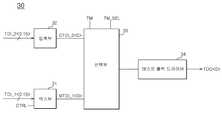
도 2는 본 발명의 실시예에 따른 반도체 장치의 블록도로서, 데이터를 외부로 출력하는 데이터 출력 경로에 대하여 도시하고 있다.2 is a block diagram of a semiconductor device according to an embodiment of the present invention, showing a data output path for outputting data to the outside.
도 2의 반도체 장치는 데이터 출력부(10), 입출력 패드(20), 테스트 출력부(30) 및 프로브 패드(40)를 포함한다.2 includes a
상기 데이터 출력부(10)는 데이터 라인(GIO)으로부터 전송되는 전송 데이터(DI)를 수신하여 외부로 출력하기 위한 출력 데이터(DO)를 생성한다. 구체적으로, 데이터 출력부(10)는 데이터를 클럭에 동기시켜 출력하는 플립플랍, 데이터를 구동하는 출력 드라이버 등의 회로를 포함할 수 있다.The
상기 입출력 패드(20)는 출력 데이터(DO)를 외부로 출력하는 패드이다. 본 실시예에서는 상기 입출력 패드(20)로 출력 로드가 작은 패드를 사용하는 데, 일 예로 범프(bump) 패드를 사용할 수 있다. 입출력 패드(20)의 출력 로드가 작기 때문에, 상기 데이터 출력부(10)의 구동력 또한 작게 설정된다.The input /
상기 테스트 출력부(30)는 테스트 모드 신호(TM)에 응답하여 활성화되고, 테스트 선택 신호(TM_SEL)에 응답하여 전송 데이터(DI)를 제 1 테스트 입력 데이터(TDI_1)로 수신하거나, 출력 데이터(DO)를 제 2 테스트 입력 데이터(TDI_2)로 수신한다. 즉, 테스트 출력부(30)가 활성화된 상태에서, 제 1 레벨의 테스트 선택 신호(TM_SEL)가 인가되면 전송 데이터(DI)를 수신하여 이를 테스트 데이터(TDO)로서 프로브 패드(40)로 출력하고, 제 2 레벨의 테스트 선택 신호(TM_SEL)가 인가되면 입출력 패드(20)로부터 출력 데이터(DO)를 수신하여 이를 테스트 데이터(TDO)로서 프로브 패드(40)로 출력한다.The
상기 프로브 패드(40)는 테스트 데이터(TDO)를 외부로 출력하는 패드이다. 프로브 패드(40)는 프로브 테스트를 위해 별도로 구비된 패드이기 때문에, 상기 입출력 패드(20)보다 출력 로드가 크게 설정된다. 프로브 패드(40)의 출력 로드가 비교적 크기 때문에, 테스트 출력부(30)의 구동력은 상기 데이터 출력부(10)의 구동력 보다 크게 설정된다.The
본 발명의 실시예에 따른 반도체 장치의 동작을 설명하면 다음과 같다.The operation of the semiconductor device according to the embodiment of the present invention will now be described.
우선, 노멀 동작 시 데이터 리드 동작과 같은 데이터 출력 동작을 수행하는 경우, 예컨대 메모리 셀에 저장된 데이터가 데이터 라인(GIO)을 통해 데이터 출력부(10)로 전송된다. 데이터 출력부(10)는 전송 데이터(DI)를 수신하여 출력 데이터(DO)로서 입출력 패드(20)로 출력한다. 이때, 테스트 모드 신호(TM)가 비활성화되어 테스트 출력부(30)로 인가되므로, 테스트 출력부(30)는 비활성화 상태가 된다.First, when performing a data output operation such as a data read operation in a normal operation, for example, data stored in a memory cell is transferred to the
테스트 모드 시, 데이터 리드 동작과 같은 데이터 출력 동작을 수행하는 경우, 마찬가지로 예컨대 메모리 셀에 저장된 데이터가 데이터 라인(GIO)을 통해 데이터 출력부(10)로 전송된다. 데이터 출력부(10)는 전송 데이터(DI)를 수신하여 출력 데이터(DO)로서 입출력 패드(20)로 출력한다.In the test mode, when a data output operation such as a data read operation is performed, data stored in, for example, a memory cell is transferred to the
이때, 테스트 모드 신호(TM)가 활성화되어 테스트 출력부(30)로 인가되기 때문에, 테스트 출력부(30)는 활성화 상태가 된다. 테스트 선택 신호(TM_SEL)에 응답하여 테스트 출력부(30)의 동작 모드가 결정된다. 예컨대, 제 1 레벨의 테스트 선택 신호(TM_SEL)가 인가되면, 테스트 출력부(30)는 제 1 모드로 동작하여 데이터 라인(GIO)을 통해 전송되는 전송 데이터(DI)를 수신하여 테스트 데이터(TDO)로서 출력한다. 반면, 제 2 레벨의 테스트 선택 신호(TM_SEL)가 인가되면, 테스트 출력부(30)는 제 2 모드로 동작하여 입출력 패드(20)로 출력되는 출력 데이터(DO)를 수신하여 테스트 데이터(TDO)로 출력한다.At this time, since the test mode signal TM is activated and applied to the
요약하면, 본 발명의 실시예에 따른 반도체 장치는 테스트 출력부(30)를 통해 데이터 라인(GIO)으로 전송되는 전송 데이터(DI) 또는 입출력 패드(20)로 출력되는 출력 데이터(DO)를 프로브 패드(40)로 출력하여 프로브 테스트를 수행할 수 있다. 즉, 제 1 모드에서는 예컨대 데이터 라인(GIO)에 실린 메모리 셀에 저장된 데이터에 대한 프로브 테스트를 수행함으로써 메모리 셀 불량을 검증할 수 있고, 제 2 모드에서는 출력 경로를 거쳐 입출력 패드(20)로 출력되는 데이터에 대한 프로브 테스트를 수행함으로써 데이터 출력 경로 불량을 검증할 수 있다.The semiconductor device according to the embodiment of the present invention includes transmission data DI transmitted to the data line GIO through the
예컨대, 제 1 모드의 테스트 모드에서 출력되는 테스트 데이터(TDO)가 설정 값으로 출력된다면 이는 메모리 셀에 불량이 없음을 의미한다. 그러나 이때 제 2 모드의 테스트 모드에서 출력되는 테스트 데이터(TDO)가 비설정 값으로 출력된다면 이를 통해 데이터 출력 경로에 불량이 존재함을 알 수 있다.For example, if the test data (TDO) output in the test mode of the first mode is output as a set value, it means that there is no defect in the memory cell. However, if the test data (TDO) outputted in the test mode of the second mode is outputted as a non-set value at this time, it is found that there is a defect in the data output path.
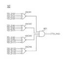
도 3은 상기 테스트 출력부(30)의 구체적인 실시예를 나타내는 블록도이다.3 is a block diagram showing a specific embodiment of the
상기 테스트 출력부(30)는 먹스부(31), 압축부(32), 선택부(33) 및 테스트 출력 드라이버(34)를 포함한다.The
상기 먹스부(31)는 제어 신호(CTRL)에 응답하여 복수의 제 1 테스트 입력 데이터(TDI_1<0:15>) 중 어느 하나를 선택 전송 데이터(MTDI_1<0>)로 출력한다. 복수의 제 1 테스트 입력 데이터(TDI_1<0:15>)는 복수의 데이터 라인(GIO)을 통해 전송되는 복수의 전송 데이터(DI)에 해당한다. 제어 신호(CTRL)는 복수의 제 1 테스트 입력 데이터(TDI_1<0:15>) 중 어느 하나를 선택하기 위하여 인가되는 것으로, 제어 신호(CTRL)을 가변시킴으로써 모든 제 1 테스트 입력 데이터(TDI_1<0:15>)에 대한 테스트를 수행할 수 있다. 본 발명의 실시예에 따른 반도체 장치는 먹스부(31)를 통해 데이터를 선택적으로 테스트 할 수 있기 때문에, 입출력 패드(20)보다 적은 개수의 프로브 패드(40)만으로 모든 데이터에 대한 테스트를 수행할 수 있다.The
상기 압축부(32)는 복수의 제 2 테스트 입력 데이터(TDI_2<0:15>)를 압축하여 압축 데이터(CTDI_2<0>)로 출력한다. 압축 기법은 동시에 복수의 데이터를 검증하고자 할 때 사용되는 것으로, 예컨대 상기 복수의 제 2 테스트 입력 데이터(TDI_2<0:15>)가 모두 동일한 레벨일 경우 제 1 레벨의 압축 데이터(CTDI_2<0>)를 생성하도록 하고, 그렇지 않으면 제 2 레벨의 상기 압축 데이터(CTDI_2<0>)를 생성하도록 하는 방식으로 설정될 수 있다. 즉, 모두 동일한 레벨의 데이터가 출력되도록 설정되어 있다면, 반도체 장치에 불량이 없는 경우 제 1 레벨의 압축 데이터(CTDI_2<0>)를 출력할 것이고, 반도체 장치에 불량이 존재하여 데이터 레벨에 영향을 끼칠 경우 제 2 레벨의 압축 데이터(CTDI_2<0>)를 출력할 것이다.The
상기 선택부(33)는 테스트 모드 신호(TM)에 응답하여 활성화되고, 테스트 선택 신호(TM_SEL)에 응답하여 선택 전송 데이터(MTDI_1<0>)를 수신하여 출력하거나, 압축 데이터(CTDI_2<0>)를 수신하여 출력한다. 즉, 선택부(33)가 활성화된 상태에서, 제 1 레벨의 테스트 선택 신호(TM_SEL)가 인가되면 선택 전송 데이터(MTDI_1<0>)를 선택하여 출력하고, 제 2 레벨의 테스트 선택 신호(TM_SEL)가 인가되면 압축 데이터(CTDI_2<0>)를 수신하여 출력한다.The
상기 테스트 출력 드라이버(34)는 상기 선택부(33)의 출력을 수신하여 이를 테스트 데이터(TDO<0>)로 구동하여 프로브 패드(40)로 출력한다.The
도 4는 상기 압축부(32)의 구체적인 일 실시예를 나타내는 회로도이다.4 is a circuit diagram showing a specific embodiment of the
상기 압축부(32)는 제 1 내지 제 4 배타적 논리 부정합 소자(XNOR1~4) 및 앤드 게이트(AD1)를 포함한다.The
각각의 배타적 논리 부정합 소자(XNOR1~4)는 각각 소정 개수의 제 1 테스트 입력 데이터(TDI_1<0:15>)를 수신하여 배타적 논리 부정합 연산을 수행한다. 배타적 논리 부정합 소자는 복수의 입력 값의 레벨이 모두 동일한 경우에는 하이 레벨의 출력 신호를 생성하고, 복수의 입력 갑의 레벨 중 어느 하나라도 상이한 경우에는 로우 레벨의 출력 신호를 생성한다. 예컨대, 각각의 논리 부정합 소자(XNOR1~4)는 4-input의 소자로서, 제 1 논리 부정합 소자(XNOR1)는 TDI_2<0> 내지 TDI_2<3>에 대한 배타적 논리 부정합 연산을 수행하고, 제 2 논리 부정합 소자(XNOR2)는 TDI_2<4> 내지 TDI_2<7>에 대한 배타적 논리 부정합 연산을 수행하며, 제 3 논리 부정합 소자(XNOR3)는 TDI_2<8> 내지 TDI_2<11>에 대한 배타적 논리 부정합 연산을 수행하고, 제 4 논리 부정합 소자(XNOR4)는 TDI_2<12> 내지 TDI_2<15>에 대한 배타적 논리 부정합 연산을 수행한다.Each of the exclusive logical mismatching elements XNOR1 to XNOR4 receives a predetermined number of first test input data TDI_1 < 0:15 > to perform an exclusive logical mismatch operation. The exclusive logical mismatching element generates a high-level output signal when the levels of the plurality of input values are all the same, and generates a low-level output signal when any one of the levels of the plurality of input terminals is different. For example, each of the logical mismatch devices XNOR1 to XNOR4 is a 4-input device, the first logical mismatch device XNOR1 performs an exclusive logical mismatch operation on TDI_2 <0> to TDI_2 <3> The logical mismatch element XNOR2 performs an exclusive logical mismatch operation on TDI_2 <4> to TDI_2 <7>, and the third logical mismatch element XNOR3 performs an exclusive logical mismatch operation on TDI_2 <8> to TDI_2 < And the fourth logical mismatch element XNOR4 performs an exclusive logical mismatch operation on TDI_2 <12> to TDI_2 <15>.
앤드 게이트(AD1)는 상기 제 1 내지 제 4 배타적 논리 부정합 소자(XNOR1~4)의 출력을 수신하여 앤드 조합하여 압축 데이터(CTDI_2<0>)로서 출력한다. 상기 제 1 내지 제 4 배타적 논리 부정합 소자(XNOR1~4)의 출력이 모두 하이 레벨인 경우에는 하이 레벨의 압축 데이터(CTDI_2<0>)를 생성하나, 상기 제 1 내지 제 4 배타적 논리 부정합 소자(XNOR1~4)의 출력 중 어느 하나라도 로우 레벨인 경우에는 로우 레벨의 압축 데이터(CTDI_2<0>)를 생성한다.The AND gate AD1 receives and combines the outputs of the first to fourth exclusive logical mismatching elements XNOR1 to XNOR4 and outputs the resultant as compressed data CTDI_2 <0>. Level compressed data CTDI_2 <0> when the outputs of the first to fourth exclusive logical mismatching devices XNOR1 to XNOR4 are all at a high level, but the first to fourth exclusive logical mismatching devices Level compressed data CTDI_2 < 0 >) when any one of the outputs of the XOR gates XNOR1 to XNOR4 is at the low level.
도 5는 본 발명의 실시예에 따른 반도체 장치의 데이터 출력 경로 테스트 방법을 나타내는 순서도이다.5 is a flowchart showing a data output path test method of a semiconductor device according to an embodiment of the present invention.
테스트 모드에서 우선 메모리 셀에 데이터를 라이트하는 동작을 수행한다. 활성화된 라이트 명령(WRITE)이 인가되면(S1), 복수의 메모리 셀에 하이 레벨 또는 로우 레벨의 동일한 데이터를 라이트 한다(S1_1).In the test mode, data is written to the memory cell first. When the activated write command WRITE is applied (S1), the same data of a high level or a low level is written in a plurality of memory cells (S1_1).
이후 라이트된 데이터에 대한 리드 동작을 수행한다. 활성화된 리드 명령(READ)이 인가되면(S2), 상기 복수의 메모리 셀에 라이트된 데이터가 데이터 출력 회로를 거쳐 입출력 패드로 출력된다(S2_1). 이렇게 입출력 패드로 출력된 데이터를 프로브 패드를 통하여 외부로 출력함으로써 데이터 출력 경로의 불량을 할 수 있다. 다만, 설계의 효율을 위해 프로브 패드의 개수는 한정적이기 때문에, 이렇게 입출력 패드로 출력된 복수의 데이터를 압축하는 단계가 추가될 수 있다(S2_2). 압축은 앞서 설명한 바와 같이, 복수의 데이터 레벨이 모두 동일한 경우에는 제 1 레벨의 압축 데이터를 생성하고, 복수의 데이터 레벨 중 어느 하나라도 상이한 경우에는 제 2 레벨의 압축 데이터를 생성하는 방식으로 수행된다. 이러한 압축 데이터를 테스트 데이터로서 프로브 패드로 출력(S2_3)하고, 상기 테스트 데이터를 외부에서 프로빙함으로써 데이터 출력 경로에 대한 프로브 테스트를 수행할 수 있다.And then performs a read operation on the written data. When the activated read command READ is applied (S2), the data written in the plurality of memory cells is output to the input / output pad via the data output circuit (S2_1). By outputting the data output through the input / output pad to the outside via the probe pad, the data output path can be defective. However, since the number of probe pads is limited for the efficiency of design, a step of compressing a plurality of data output to the input / output pad may be added (S2_2). As described above, compression is performed in such a manner that compressed data of a first level is generated when a plurality of data levels are identical to each other, and compressed data of a second level is generated when any one of a plurality of data levels is different . The compressed data is outputted to the probe pad as test data (S2_3), and the probe test on the data output path can be performed by probing the test data from the outside.
따라서, 본 발명의 실시예에 따르면, 반도체 메모리 장치의 데이터 출력 경로의 불량에 대한 검증을 수행할 수 있다. 당업자라면, 메모리 셀 불량 테스트를 수행하여 메모리 셀 불량이 없음이 검증되었고, 이후 데이터 출력 경로 테스트를 수행하여 테스트 데이터를 통해 불량이 존재함을 확인하였다면, 이를 통해 출력 드라이버 내지는 출력 회로를 포함하는 데이터 출력 경로에 불량이 존재함을 알 수 있을 것이다.Therefore, according to the embodiment of the present invention, it is possible to perform verification of the failure of the data output path of the semiconductor memory device. Those skilled in the art will appreciate that if a memory cell failure test has been performed to verify that there is no memory cell failure and then a data output path test is performed to confirm that there is a failure through the test data, It can be seen that there is a defect in the output path.
본 발명이 속하는 기술분야의 당업자는 본 발명이 그 기술적 사상이나 필수적 특징을 변경하지 않고서 다른 구체적인 형태로 실시될 수 있으므로, 이상에서 기술한 실시예들은 모든 면에서 예시적인 것이며 한정적인 것이 아닌 것으로서 이해해야만 한다. 본 발명의 범위는 상기 상세한 설명보다는 후술하는 특허청구범위에 의하여 나타내어지며, 특허청구범위의 의미 및 범위 그리고 그 등가개념으로부터 도출되는 모든 변경 또는 변형된 형태가 본 발명의 범위에 포함되는 것으로 해석되어야 한다.It will be understood by those skilled in the art that various changes in form and details may be made therein without departing from the spirit and scope of the present invention as defined by the following claims and their equivalents. Only. The scope of the present invention is defined by the appended claims rather than the detailed description and all changes or modifications derived from the meaning and scope of the claims and their equivalents are to be construed as being included within the scope of the present invention do.
10 : 데이터 출력부 20 : 입출력 패드
30 : 데이터 출력부 40 : 프로브 패드
31 : 먹스부 32 : 먹스부
33 : 선택부 34 : 테스트 출력 드라이버10: Data output unit 20: Input / output pad
30: Data output unit 40: Probe pad
31: Mux 32: Mux
33: Selector 34: Test output driver
Claims (12)
Translated fromKorean상기 테스트 출력부는,
상기 데이터 출력 경로 테스트 모드 시 복수의 상기 입출력 패드로 출력되는 복수의 상기 출력 데이터를 수신하고, 이를 압축한 압축 데이터를 상기 프로브 패드로 출력하는 반도체 장치.The method according to claim 1,
The test-
And a plurality of output data output to the plurality of input / output pads in the data output path test mode, and outputs the compressed data compressed by the plurality of output data to the probe pads.
상기 테스트 출력부는,
상기 복수의 출력 데이터가 모두 동일한 레벨일 경우 제 1 레벨의 상기 압축 데이터를 생성하고, 그렇지 않으면 제 2 레벨의 상기 압축 데이터를 생성하는 반도체 장치.3. The method of claim 2,
The test-
And generates the compressed data of the first level when the plurality of output data are all at the same level, and otherwise generates the compressed data of the second level.
테스트 모드 시, 상기 전송 데이터 및 상기 입출력 패드로 출력 되는 출력 데이터 중 어느 하나를 수신하여 프로브 패드로 출력하는 테스트 출력부를 포함하는 반도체 장치.A data output unit for outputting transmission data transmitted through a data line to an input / output pad; And
And a test output unit for receiving one of the transmission data and the output data output to the input / output pad and outputting the received data to the probe pad in a test mode.
상기 테스트 출력부는,
테스트 모드 신호에 응답하여 활성화되는 반도체 장치.5. The method of claim 4,
The test-
And is activated in response to a test mode signal.
상기 테스트 출력부는,
테스트 선택 신호에 응답하여 제 1 모드 시 상기 전송 데이터를 수신하여 상기 프로브 패드로 출력하고, 제 2 모드 시 상기 출력 데이터를 수신하여 상기 프로브 패드로 출력하는 반도체 장치.6. The method of claim 5,
The test-
Receiving the transmission data in a first mode in response to a test selection signal and outputting the transmission data to the probe pad in a first mode and receiving the output data in a second mode and outputting the output data to the probe pad.
상기 테스트 출력부는,
제어 신호에 응답하여 복수의 상기 데이터 라인을 통해 전송되는 복수의 상기 전송 데이터 중 어느 하나를 선택 전송 데이터로 출력하는 먹스부;
복수의 상기 입출력 패드로 출력되는 복수의 상기 출력 데이터를 압축하여 압축 데이터로 출력하는 압축부;
활성화된 테스트 모드 신호가 인가되면, 테스트 선택 신호에 응답하여 상기 선택 전송 데이터 및 상기 압축 데이터 중 어느 하나를 출력하는 선택부; 및
상기 선택부의 출력을 테스트 데이터로서 상기 프로브 패드로 출력하는 테스트 출력 드라이버를 포함하는 반도체 장치.5. The method of claim 4,
The test-
A multiplexer for outputting any one of the plurality of transmission data transmitted through the plurality of data lines in response to a control signal as selective transmission data;
A compression unit that compresses a plurality of output data output from the plurality of input / output pads and outputs the compressed data as compressed data;
A selection unit for outputting either the selected transmission data or the compressed data in response to a test selection signal when an activated test mode signal is applied; And
And a test output driver for outputting the output of the selector as test data to the probe pad.
상기 압축부는,
상기 복수의 출력 데이터가 모두 동일한 레벨일 경우 제 1 레벨의 상기 압축 데이터를 생성하고, 그렇지 않으면 제 2 레벨의 상기 압축 데이터를 생성하는 반도체 장치.8. The method of claim 7,
Wherein the compression unit comprises:
And generates the compressed data of the first level when the plurality of output data are all at the same level, and otherwise generates the compressed data of the second level.
상기 선택부는,
상기 테스트 선택 신호에 응답하여 제 1 모드 시 상기 선택 전송 데이터를 선택하여 출력하고, 제 2 모드 시 상기 압축 데이터를 선택하여 출력하는 반도체 장치.8. The method of claim 7,
Wherein the selection unit comprises:
Selects and outputs the selected transmission data in a first mode in response to the test selection signal, and selects and outputs the compressed data in a second mode.
상기 복수의 메모리 셀에 라이트된 상기 데이터를 리드(read)하여 입출력 패드로 출력하는 단계; 및
상기 입출력 패드로 출력되는 출력 데이터를 프로브 패드로 출력하는 단계를 포함하는 반도체 장치의 테스트 방법.Collectively writing data of a same level to a plurality of memory cells;
Reading the data written in the plurality of memory cells and outputting the read data to an input / output pad; And
And outputting the output data output to the input / output pad to a probe pad.
상기 프로브 패드로 출력하는 단계는,
복수의 상기 입출력 패드로 출력되는 복수의 출력 데이터를 압축하여 압축 데이터를 생성하는 단계; 및
상기 압축 데이터를 테스트 데이터로서 상기 프로브 패드로 출력하는 단계를 포함하는 반도체 장치의 테스트 방법.11. The method of claim 10,
Wherein the step of outputting to the probe pad comprises:
Outputting a plurality of output data to a plurality of input / output pads to generate compressed data; And
And outputting the compressed data as test data to the probe pad.
상기 압축 데이터를 생성하는 단계는,
상기 복수의 출력 데이터가 모두 동일한 레벨일 경우 제 1 레벨의 상기 압축 데이터를 생성하고, 그렇지 않으면 제 2 레벨의 상기 압축 데이터를 생성하는 반도체 장치의 테스트 방법.12. The method of claim 11,
Wherein the step of generating compressed data comprises:
And generating the compressed data of the first level when the plurality of output data are all at the same level, and otherwise generating the compressed data of the second level.
Priority Applications (2)
| Application Number | Priority Date | Filing Date | Title |
|---|---|---|---|
| KR1020120130883AKR20140064025A (en) | 2012-11-19 | 2012-11-19 | Semiconductor apparatus and test method thereof |
| US13/846,132US20140143620A1 (en) | 2012-11-19 | 2013-03-18 | Semiconductor apparatus and test method thereof |
Applications Claiming Priority (1)
| Application Number | Priority Date | Filing Date | Title |
|---|---|---|---|
| KR1020120130883AKR20140064025A (en) | 2012-11-19 | 2012-11-19 | Semiconductor apparatus and test method thereof |
Publications (1)
| Publication Number | Publication Date |
|---|---|
| KR20140064025Atrue KR20140064025A (en) | 2014-05-28 |
Family
ID=50729140
Family Applications (1)
| Application Number | Title | Priority Date | Filing Date |
|---|---|---|---|
| KR1020120130883AWithdrawnKR20140064025A (en) | 2012-11-19 | 2012-11-19 | Semiconductor apparatus and test method thereof |
Country Status (2)
| Country | Link |
|---|---|
| US (1) | US20140143620A1 (en) |
| KR (1) | KR20140064025A (en) |
Families Citing this family (1)
| Publication number | Priority date | Publication date | Assignee | Title |
|---|---|---|---|---|
| KR101208960B1 (en)* | 2010-11-26 | 2012-12-06 | 에스케이하이닉스 주식회사 | Semiconductor apparatus and test method thereof |
- 2012
- 2012-11-19KRKR1020120130883Apatent/KR20140064025A/ennot_activeWithdrawn
- 2013
- 2013-03-18USUS13/846,132patent/US20140143620A1/ennot_activeAbandoned
Also Published As
| Publication number | Publication date |
|---|---|
| US20140143620A1 (en) | 2014-05-22 |
Similar Documents
| Publication | Publication Date | Title |
|---|---|---|
| US20070241766A1 (en) | Semiconductor integrated circuit | |
| US8867287B2 (en) | Test circuit and method of semiconductor memory apparatus | |
| TWI660183B (en) | Component inspection method, probe card, interposer and inspection device | |
| KR20150097074A (en) | Test circuit and semiconductor apparatus including the same | |
| KR20150005297A (en) | Parallel test device and method | |
| KR101143443B1 (en) | Semiconductor apparatus and its repairing method | |
| US7202692B2 (en) | Semiconductor chip and method of testing the same | |
| US20080077830A1 (en) | Internal signal monitoring device in semiconductor memory device and method for monitoring the same | |
| CN113097198B (en) | Stacked semiconductor device and test method thereof | |
| CN112562770B (en) | Semiconductor device with test circuit | |
| KR102805977B1 (en) | Memory device and test operation thereof | |
| KR20210080928A (en) | Stacked semiconductor device and test method thereof | |
| US20240412799A1 (en) | Circuits And Methods For Memory Built-In-Self-Tests | |
| KR101282722B1 (en) | Memory device and test method for memory device | |
| CN112599183B (en) | Apparatus and method for providing a clock to a data path | |
| US9299403B2 (en) | Semiconductor devices and semiconductor systems including the same | |
| KR20140064025A (en) | Semiconductor apparatus and test method thereof | |
| KR20110002678A (en) | Semiconductor memory device and test method thereof | |
| CN101915892B (en) | Chip test circuit | |
| CN103886914B (en) | Channel control circuit and the semiconductor devices with channel control circuit | |
| KR20140075347A (en) | Semiconductor apparatus | |
| KR100728564B1 (en) | Test mode signal generator of semiconductor memory device | |
| KR20120080352A (en) | Semiconductor memory apparatus, check circuit for parallel test therefor | |
| KR20110108558A (en) | Semiconductor memory device and compression test method | |
| KR101124282B1 (en) | Parallel compression tester of a memory device |
Legal Events
| Date | Code | Title | Description |
|---|---|---|---|
| PA0109 | Patent application | Patent event code:PA01091R01D Comment text:Patent Application Patent event date:20121119 | |
| PG1501 | Laying open of application | ||
| PC1203 | Withdrawal of no request for examination | ||
| WITN | Application deemed withdrawn, e.g. because no request for examination was filed or no examination fee was paid |