KR20140061982A - Usb peripheral device detection on an unpowered bus - Google Patents
Usb peripheral device detection on an unpowered busDownload PDFInfo
- Publication number
- KR20140061982A KR20140061982AKR20130138350AKR20130138350AKR20140061982AKR 20140061982 AKR20140061982 AKR 20140061982AKR 20130138350 AKR20130138350 AKR 20130138350AKR 20130138350 AKR20130138350 AKR 20130138350AKR 20140061982 AKR20140061982 AKR 20140061982A
- Authority
- KR
- South Korea
- Prior art keywords
- voltage
- power line
- bus
- nominal
- usb
- Prior art date
- Legal status (The legal status is an assumption and is not a legal conclusion. Google has not performed a legal analysis and makes no representation as to the accuracy of the status listed.)
- Granted
Links
Images


Classifications
- G—PHYSICS
- G01—MEASURING; TESTING
- G01R—MEASURING ELECTRIC VARIABLES; MEASURING MAGNETIC VARIABLES
- G01R19/00—Arrangements for measuring currents or voltages or for indicating presence or sign thereof
- G01R19/165—Indicating that current or voltage is either above or below a predetermined value or within or outside a predetermined range of values
- G—PHYSICS
- G01—MEASURING; TESTING
- G01R—MEASURING ELECTRIC VARIABLES; MEASURING MAGNETIC VARIABLES
- G01R31/00—Arrangements for testing electric properties; Arrangements for locating electric faults; Arrangements for electrical testing characterised by what is being tested not provided for elsewhere
- G01R31/28—Testing of electronic circuits, e.g. by signal tracer
- G01R31/2832—Specific tests of electronic circuits not provided for elsewhere
- G—PHYSICS
- G06—COMPUTING OR CALCULATING; COUNTING
- G06F—ELECTRIC DIGITAL DATA PROCESSING
- G06F13/00—Interconnection of, or transfer of information or other signals between, memories, input/output devices or central processing units
- G06F13/38—Information transfer, e.g. on bus
- G06F13/40—Bus structure
- G06F13/4063—Device-to-bus coupling
- G06F13/4068—Electrical coupling
- G06F13/4072—Drivers or receivers
- G—PHYSICS
- G06—COMPUTING OR CALCULATING; COUNTING
- G06F—ELECTRIC DIGITAL DATA PROCESSING
- G06F13/00—Interconnection of, or transfer of information or other signals between, memories, input/output devices or central processing units
- G06F13/38—Information transfer, e.g. on bus
- G06F13/40—Bus structure
- G06F13/4063—Device-to-bus coupling
- G06F13/4068—Electrical coupling
- G06F13/4081—Live connection to bus, e.g. hot-plugging
- G—PHYSICS
- G06—COMPUTING OR CALCULATING; COUNTING
- G06F—ELECTRIC DIGITAL DATA PROCESSING
- G06F2213/00—Indexing scheme relating to interconnection of, or transfer of information or other signals between, memories, input/output devices or central processing units
- G06F2213/0042—Universal serial bus [USB]
- Y—GENERAL TAGGING OF NEW TECHNOLOGICAL DEVELOPMENTS; GENERAL TAGGING OF CROSS-SECTIONAL TECHNOLOGIES SPANNING OVER SEVERAL SECTIONS OF THE IPC; TECHNICAL SUBJECTS COVERED BY FORMER USPC CROSS-REFERENCE ART COLLECTIONS [XRACs] AND DIGESTS
- Y02—TECHNOLOGIES OR APPLICATIONS FOR MITIGATION OR ADAPTATION AGAINST CLIMATE CHANGE
- Y02D—CLIMATE CHANGE MITIGATION TECHNOLOGIES IN INFORMATION AND COMMUNICATION TECHNOLOGIES [ICT], I.E. INFORMATION AND COMMUNICATION TECHNOLOGIES AIMING AT THE REDUCTION OF THEIR OWN ENERGY USE
- Y02D10/00—Energy efficient computing, e.g. low power processors, power management or thermal management
Landscapes
- Engineering & Computer Science (AREA)
- General Engineering & Computer Science (AREA)
- Theoretical Computer Science (AREA)
- Physics & Mathematics (AREA)
- General Physics & Mathematics (AREA)
- Computer Hardware Design (AREA)
- Power Sources (AREA)
- Debugging And Monitoring (AREA)
- Bus Control (AREA)
- Direct Current Feeding And Distribution (AREA)
Abstract
Translated fromKoreanDescription
Translated fromKorean본 발명은 전력 라인을 구비한 통신 인터페이스를 포함하는 가정용 전자 장비의 분야에 관한 것이다. 구체적으로, 본 발명은 전력 라인이 활성화되지 않을 때 인터페이스에 대한 주변 장비의 아이템의 접속을 검출하기 위한 방법에 관한 것이다.The present invention relates to the field of household electronic equipment comprising a communication interface with power lines. Specifically, the present invention relates to a method for detecting connection of items of peripheral equipment to an interface when a power line is not activated.
USB 인터페이스를 특성화하는 장비의 아이템에 대한 USB 주변 장치의 접속을 검출할 수 있는 방법들이 존재한다. 첫 번째 방법은 USB 버스의 데이터 라인들의 전위들의 변화들을 검출하는 것이며, 이들 라인은 풀업(pull-up) 또는 풀다운(pull-down) 저항기들을 구비한다. 다른 방법은 USB 버스의 명목 전압 V_BUS에 대응하는 전위가 제품의 USB 인터페이스 상에 출현하는지를 검출하는 것이다.There are ways to detect the connection of a USB peripheral to an item of equipment that characterizes the USB interface. The first method is to detect changes in the potentials of the data lines of the USB bus, these lines having pull-up or pull-down resistors. Another method is to detect whether a potential corresponding to the nominal voltage V_BUS of the USB bus appears on the USB interface of the product.
특정 방법들은 스캐닝되는 피더 라인들 또는 데이터 라인들의 상이한 전위들(또는 상태들)이 구별될 수 있도록 회로들이 급전되는 것을 필요로 한다. 다른 방법들은 USB 인터페이스와 인터페이스에 접속된 주변 장치 사이에서 프로토콜에 따라 데이터 교환들이 가능하도록 USB 버스에 명목상 급전하는 것을 필요로 한다.Certain methods require that the circuits be powered so that the different potentials (or states) of the feeder lines or data lines being scanned can be distinguished. Other methods require nominally feeding the USB bus so that data can be exchanged between the USB interface and peripherals connected to the interface according to the protocol.
그러나, 가정용 장비들의 전기 소비를 줄여야 하는 제약이 점점 더 커지고 있으며, 그들의 전기 소비를 줄이기 위해 다가오는 수년 내에 적용되어야 하는 공적 지령은 가능한 어느 곳에서나 소비를 줄일 것을 요구한다.However, the constraints of reducing the electricity consumption of household appliances are increasingly increasing, and the public order to be applied within the coming years to reduce their electricity consumption requires that consumption be reduced wherever possible.
본 발명은 특히 장비의 아이템이 저소비 모드로 또는 스탠바이 모드로 구성됨으로 인해 장비의 아이템의 USB 인터페이스가 그의 명목 전압에 의해 급전되지 않을 때 또는 인터페이스의 명목 전압이 인가되지 않을 때 그리고 잔여 전압이 인터페이스의 전력 라인 상에 존재할 때 장비의 아이템의 USB 인터페이스에 대한 USB 주변 장치의 접속을 검출하기 위한 방법을 제안함으로써 상황을 개선할 수 있다.The present invention is particularly advantageous when the USB interface of an item of equipment is not powered by its nominal voltage due to the item of equipment being configured in a low consumption mode or in a standby mode, or when the nominal voltage of the interface is not applied, The situation can be improved by suggesting a method for detecting the connection of the USB peripheral to the USB interface of the item of equipment when it is on the power line.
더 구체적으로, 본 발명은 전자 장치의 통신 인터페이스에 대한 주변 장치의 접속을 검출하기 위한 방법에 관한 것으로서, 상기 통신 인터페이스는 상기 주변 장치에 전력을 공급하기 위한 전압 전력 라인을 포함하고, 동작 전압 값들의 범위 내의 명목 값이 상기 전력 라인과 관련되며, 상기 방법은More specifically, the present invention relates to a method for detecting a connection of a peripheral device to a communication interface of an electronic device, the communication interface comprising a voltage power line for powering the peripheral device, Wherein a nominal value within the range of the power line is associated with the power line,
- 상기 전자 장치에 의해, 상기 전력 라인의 상기 동작 전압 값들의 범위 사이에 포함되는 명목 전압을 인가하는 단계,- applying, by the electronic device, a nominal voltage comprised between a range of the operating voltage values of the power line,
- 상기 전자 장치에 의해, 상기 전력 라인에 인가되는 상기 명목 동작 전압을 중단하는 단계,- stopping, by the electronic device, the nominal operating voltage applied to the power line,
- 상기 전력 라인 상에서, 상기 명목 전압 값의 임계치보다 낮은 잔여 전압의 존재시에, 상기 인터페이스에 대한 상기 주변 장치의 상기 접속으로부터 발생하는 과도 신호(transient signal)를 검출하는 단계,Detecting on the power line a transient signal resulting from the connection of the peripheral device to the interface in the presence of a residual voltage lower than a threshold of the nominal voltage value,
- 검출된 상기 과도 신호에 따라 제어 신호를 생성하는 단계,Generating a control signal in accordance with the detected transient signal,
- 생성된 상기 제어 신호에 따라 상기 명목 전압을 상기 전압 전력 라인에 인가하는 단계- applying the nominal voltage to the voltage power line according to the generated control signal
를 포함한다..
예를 들어, USB 통신 인터페이스의 경우, 전력 라인은 일반적으로 V_BUS로 지칭된다.For example, in the case of a USB communication interface, the power line is commonly referred to as V_BUS.
본 발명의 일 실시예에 따르면, 상기 통신 인터페이스는 유니버설 직렬 버스(Universal Serial Bus) 표준에 적합하다.According to an embodiment of the present invention, the communication interface is compliant with the Universal Serial Bus standard.
본 발명의 일 실시예에 따르면, 상기 잔여 전압은 전용 전력 공급 회로에 의해 생성된다.According to an embodiment of the present invention, the residual voltage is generated by a dedicated power supply circuit.
본 발명의 일 실시예에 따르면, 상기 임계치는 상기 명목 전압의 10% 이하이다.According to an embodiment of the present invention, the threshold value is 10% or less of the nominal voltage.
본 발명의 일 실시예에 따르면, 상기 과도 신호는 상기 잔여 전압의 전압 강하이다.According to an embodiment of the present invention, the transient signal is a voltage drop of the residual voltage.
본 발명은 전자 장치에서 전력을 공급하고, 상기 전자 장치의 통신 인터페이스에 대한 주변 장치의 접속을 검출하기 위한 회로에 관한 것으로서, 상기 통신 인터페이스는 상기 주변 장치에 전력을 공급하기 위한 전압 전력 라인을 포함하고, 동작 전압 값들의 명목 범위가 상기 전력 라인과 관련되며, 상기 검출 회로는The present invention relates to a circuit for powering an electronic device and detecting a connection of a peripheral device to the communication interface of the electronic device, the communication interface including a voltage power line for powering the peripheral device , A nominal range of operating voltage values is associated with the power line, and the detection circuit
- 상기 전자 장치에 의해, 상기 전력 라인에 상기 명목 동작 전압 값들의 범위 사이에 포함되는 명목 전압을 인가하기 위한 전압 생성기 회로,- a voltage generator circuit for applying, by the electronic device, a nominal voltage comprised between the range of nominal operating voltage values to the power line,
- 상기 명목 전압 값의 임계치보다 낮은 잔여 전압의 존재시에, 상기 인터페이스에 대한 상기 주변 장치의 상기 접속으로부터 발생하는 과도 신호를 검출하는 회로,A circuit for detecting a transient signal originating from the connection of the peripheral device to the interface in the presence of a residual voltage lower than a threshold of the nominal voltage value,
- 검출된 상기 과도 신호에 따라 제어 신호를 생성하는 회로A circuit for generating a control signal in accordance with the detected transient signal;
를 포함한다..
본 발명의 일 실시예에 따르면, 상기 전압 전력 라인 V_BUS는 유니버설 직렬 버스 표준에 적합한 커넥터에 인가된다.According to one embodiment of the present invention, the voltage power line V_BUS is applied to a connector conforming to the universal serial bus standard.
본 발명은 전술한 바와 같은 전력을 공급하고 검출하기 위한 회로를 포함하는 임의의 전자 장치와 더 관련된다.The invention further relates to any electronic device comprising a circuit for supplying and detecting power as described above.
첨부된 도면들을 참조하는 아래의 설명을 읽을 때 본 발명이 더 잘 이해될 것이며, 다른 구체적인 특징들 및 장점들이 드러날 것이다. 도면들에서:
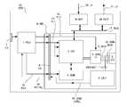
도 1은 본 발명의 일 실시예에 따른 접속 검출 회로를 구비한, USB 표준에 적합한 통신 인터페이스를 포함하는 디지털 텔레비전의 수신기-디코더 타입의 전자 장비의 아이템을 도시한다.
도 2는 도 1의 USB 인터페이스의 접속 검출 회로를 도시한다.
도 3은 도 1에 도시된 장비의 인터페이스에 대한 USB 주변 장치의 접속에 이어지는 도 2에 도시된 검출 회로에 의한 주변 장치의 검출 및 인터페이스의 활성화에 대응하는 시퀀스를 도시한다.
도 4는 검출 및 활성화 방법의 단계들을 나타내는 도면이다.BRIEF DESCRIPTION OF THE DRAWINGS The present invention will be better understood and other specific features and advantages will emerge from reading the following description with reference to the accompanying drawings. In the drawings:
BRIEF DESCRIPTION OF THE DRAWINGS Figure 1 shows an item of a receiver-decoder type electronic equipment of a digital television comprising a communication interface adapted to the USB standard, with connection detection circuitry according to an embodiment of the invention.
2 shows a connection detection circuit of the USB interface of Fig.
3 shows a sequence corresponding to the detection of the peripheral device and the activation of the interface by the detection circuit shown in Fig. 2 following the connection of the USB peripheral device to the interface of the equipment shown in Fig.
4 is a diagram showing the steps of the detection and activation method.
도 1 내지 3에서, 도시된 모듈들은 물리적으로 구별 가능한 유닛들에 대응하거나 대응하지 않을 수 있는 기능 유닛들이다. 예를 들어, 이들 모듈 또는 이들 중 일부는 단일 컴포넌트 내에 함께 그룹화되거나, 동일 소프트웨어의 기능들을 구성한다. 이와 달리, 다른 실시예들에 따르면, 일부 모듈들은 개별 물리 엔티티들(entities)로 구성된다.1 to 3, the illustrated modules are functional units that may or may not correspond to physically distinguishable units. For example, these modules, or some of them, are grouped together within a single component or make up the functions of the same software. Alternatively, according to other embodiments, some modules are configured with individual physical entities.
제한적이 아니라 일반적으로, 본 발명은 통신 인터페이스가 명목 전력을 공급받지 않을 때 통신 인터페이스에 대한 주변 장치의 접속을 검출하기 위한 방법 및 회로에 관한 것이다. 따라서, 검출은 명목 모드에서 인터페이스의 전력 공급의 활성화를 가능하게 한다. 이것은 유리하게도 주변 장치의 접속의 검출시에 통신 인터페이스의 사용을 허가하기 위해 명목 모드에서 통신 인터페이스에 전력을 공급해야 하는 것을 방지한다. 중요한 이점은 이것이 결과적으로 에너지 소비의 제한을 돕는다는 것이다.In general, and not by way of limitation, the invention relates to a method and circuit for detecting the connection of a peripheral device to a communication interface when the communication interface is not supplied with nominal power. Thus, the detection enables activation of the power supply of the interface in the nominal mode. This advantageously prevents the communication interface from being powered in the nominal mode to allow use of the communication interface upon detection of the connection of the peripheral device. An important advantage is that this helps limit energy consumption as a result.
"명목 모드"는 전압이 그의 명목 값 주위의 값들의 범위 사이에 포함되는 전력 공급 모드를 의미하는 것으로 이해한다. 일례는 5 볼트의 명목 전압에 대해 4.5 볼트 내지 5.5 볼트의 전압들의 범위 사이에 포함되는 전압의 인가이다. 본 발명의 설명에서 명목 값 전압은 그것이 급전하는 장치 또는 장치들 또는 모듈들의 정상 동작을 가능하게 하는 전압으로서 정의된다는 점에 유의해야 한다. 예를 들어, USB 통신 인터페이스에 대해, 명목 전압은 인터페이스의 명목(또는 정상) 동작에, 특히 호스트 장비와 접속된 주변 장치 사이의 데이터의 교환에 적합한 전압이다."Nominal mode" is understood to mean a power supply mode in which a voltage is included between a range of values around its nominal value. An example is the application of a voltage comprised between a range of voltages of 4.5 volts to 5.5 volts for a nominal voltage of 5 volts. It should be noted that in the description of the present invention, the nominal voltage is defined as the voltage that enables the normal operation of the device or devices or modules that it powers. For example, for a USB communication interface, a nominal voltage is a voltage suitable for nominal (or normal) operation of an interface, and in particular for exchanging data between a host device and a connected peripheral device.
도 1은 본 발명의 바람직한 실시예에 따른, 예를 들어 디지털 텔레비전의 수신기-디코더 타입의 전자 장비 STB(10)의 아이템을 도시한다. 전자 장비의 아이템은 마더보드라고도 하는 메인 보드 MB(9), 전력 공급 모듈 PSU(1), 입력 모듈 INP(18) 및 출력 모듈 OUT(19)을 포함한다. 마더보드 MB(9)는 많은 요소 가운데 특히 전력 인터페이스 USBPI(3), 버스 USB-BUS(16), 검출 회로 DET(8) 및 커넥터 USB C3(5)로 구성된 USB 통신 인터페이스를 포함한다. 검출 회로 DET(8)는 검출 버스 USB-DET에 의해 버스 USB-BUS(16)에 접속된다.1 shows an item of a receiver-decoder type
마더보드는 장비 STB(10)의 아이템을 위한 제어 및 처리 유닛으로서 작용하는 코어 회로 CU(2)를 포함한다. 마더보드 MB(9)는 스탠바이(또는 저소비) 모드 관리 회로 KDB(4)도 포함한다. 회로 KDB(4)는 마더보드 MB(9)의 인터페이스 USB의 전력 인터페이스 USB PI(3)의 전력 라인 PL2(12) 또는 심지어 마더보드 MB(9)의 제어 회로 CU(2)의 전력 라인 PL1(11)과 같은 전력 공급 모듈 PSU(1)의 출력에서의 특정 전력 라인들의 제어된 활성화를 가능하게 하는 신호 PCTRL(14)을 제어한다. 신호 PLA(13)는 전력 공급 모듈 PSU(1)의 상태, 즉 스탠바이(또는 저소비) 모드의 구성인지 아닌지를 관리 회로 KDB(4)에 알린다. 모든 라인들 PL1(11), PL2(12), PLA(13) 및 PCTRL(14)은 커넥터 C2(6)에 의해 마더보드 MB(9)에 접속된다. 주변 장치 USB의 검출 회로 DET(8)는 전력 라인들 PL1(11) 및 PL2(12)의 제어된 활성화를 가능하게 하는, 신호 PCTRL(14)에 접속된 신호 USB-CTRL(15)을 공급한다.The motherboard includes a core circuit CU (2) serving as a control and processing unit for items of equipment STB (10). The motherboard MB 9 also includes a standby (or low consumption) mode management circuit KDB (4). The circuit KDB 4 is connected to the
입력 모듈 INP(18)는 입력 링크 L1(20)에 의해 수신되는 디지털 텔레비전 신호들의 수신 및 복조에 유용한 모든 회로들을 포함한다. 출력 모듈 OUT(19)은 오디오 및 비디오 신호들을 예를 들어 텔레비전 세트와 같은 외부 복원 장치(여기에 도시되지 않음)에 공급한다. 신호들은 예를 들어 SCART 커넥터 또는 HDMI 케이블일 수 있는 링크 L2(21)에 의해 운반된다. 제어 유닛 CU(2)와 입력 INP(18) 및 출력 OUT(19) 모듈들 각각 사이에서 교환되는 모든 신호들은 상호접속 버스 BUS(17)에 의해 운반된다. 제어 회로 CU(2)는 디지털 텔레비전을 위한 시청각 프로그램들의 전송에 특정한 방법들을 이용하여 코딩된 시청각 콘텐츠의 수신 및 디코딩 기능들에 필요한 모든 회로들을 포함한다. 필터링, 디멀티플렉싱, 기억, 디코딩 및 신호 라우팅 동작들을 총체적으로 수행하는 이들 회로는, 이 분야의 기술자들에게 잘 알려져 있고 본 발명의 이해에 필요하지 않으므로 여기에 도시되지 않는다.Input module INP 18 includes all the circuits available for receiving and demodulating digital television signals received by
전력 공급 모듈 PSU(1)는 커넥터 C1(7)에 의해 본선 전류(mains current)에 의해 급전된다.The power
본 발명의 바람직한 실시예에 따르면, 전력 라인들 PL1(11) 및 PL2(12)는 수신기-디코더 장비 STB(10)가 스탠바이 모드로 구성될 때 디스에이블(disable)된다. USB 통신 인터페이스의 전력 인터페이스 USBPI(3)에 급전하는 전력 라인 PL2(12)는 명목적으로 공급되는 것이 아니라, 예를 들어 회로들의 하나 이상의 전기적 특성에 의해 존재할 수 있게 되는 잔여 전압을 운반한다. 이것은 이러한 목적을 위해 유리하게 설계되고 교정된(calibrated) 저장소 커패시터(reservoir capacitor)의 존재 또는 심지어 기생 커패시터의 적절한 이용일 수 있다.According to a preferred embodiment of the present invention, the
본 발명의 변형 실시예에 따르면, 잔여 전압은 회로들에 특정한 전기적 특성들이 아니라 이러한 용도로 설계된 특정 전력 라인(200)으로부터 온다.In accordance with an alternative embodiment of the present invention, the residual voltage comes from a
잔여 전압의 존재는 주변 장치가 커넥터 C3(5) 상에서 통신 인터페이스에 접속될 때 버스 USB-BUS(16) 상의 과도 신호의 출현에 기여한다.The presence of the residual voltage contributes to the appearance of a transient signal on bus USB-BUS 16 when the peripheral device is connected to the communication interface on connector C3 (5).
"글리치(glitch)"라고도 하는 과도 신호는 검출 회로 DET(8)에 의해 증폭되며, 교정된 신호 USB-CTRL(15)이 모듈 PSU(1)의 입력에서 제어 신호 PCTRL(14)로서 사용되게 하기 위해 검출 모듈 DET(8)의 출력에서 이용 가능하도록 포맷팅된다. 모듈 PSU(1)의 입력에서의 신호 PCTRL(14)의 활성화는 USB 통신 인터페이스에서 사용할 충분한 명목 전압을 운반하는 전력 라인 PL2(12)의 활성화, 특히 수신기-디코더 STB(10)의 제어 회로 CU2와 인터페이스 USB의 커넥터 C3(5)에 접속된 USB 주변 장치 사이의 데이터 교환의 활성화를 유도한다. 주변 장치 USB는 예를 들어 USB 키, 외부 하드 디스크 또는 통신 인터페이스와 호환되는 저장 매체일 수 있다.A transient signal, also referred to as a " glitch ", is amplified by the
도 2는 도 1에 도시된 검출 회로 DET(8)는 물론, 수신기-디코더 STB(10)가 스탠바이 또는 저소비 모드로 구성될 때를 포함하여 전력이 공급되는 것을 가능하게 하는 전력 회로(200)의 상세들을 도시한다. 전력 공급 장치(210)는 도 1에 도시된 모듈 PSU(1) 내에 포함되며, 이러한 목적을 위해 제어될 때 라인 PL2(12) 상에 명목 전압을 공급한다. 이어서, 이 명목 전압은 수신기-디코더 STB(10)의 USB 통신 인터페이스의 전력 인터페이스 USBPI(3)에 인가된다. 모듈(230)은 USB 인터페이스의 전력 라인에 접속된 USB 주변 장치를 나타낸다. 모듈(220)은 USB 인터페이스의 전력 라인의 전기적 특성들(저항 및 용량)을 나타낸다.2 is a block diagram of a
본 발명의 특정한 비제한적인 실시예에 따르면, 전력 회로(200)는 전력 회로(210)의 서브어셈블리이다.According to certain non-limiting embodiments of the present invention, the
수신기-디코더 STB(10)의 USB 소켓 C3(5) 상에 접속된 USB 주변 장치의 접속을 검출하도록 적응되는 검출 모듈 DET(8)은 3개의 메인 모듈(810, 820, 830)로 구성된다.The
모듈(810)은 USB 소켓에 대한 주변 장치의 접속의 사실로 인해 나타나는 과도 신호(또는 글리치)의 증폭에 적합한 증폭기이다.
모듈(820)은 증폭기(810)에 의해 증폭된 과도 신호로부터 피크 교정 신호를 형성하는 단안정(monostable) 모듈이다.The
모듈(830)은 USB 버스의 전력 라인이 명목 전압을 공급받을 때 출력에서의 과도 신호의 검출을 금지하는 NOR 게이트 회로를 구성한다. 수신기-디코더 장비 STB(10)가 스탠바이 모드로 구성되지 않고, USB 인터페이스(또는 버스)의 전력 라인이 명목 값 전압을 공급받을 때, 방금 접속된 주변 장치의 검출은 호스트의 주도하에, 즉 수신기-디코더 STB의 제어 유닛 CU(2)의 주도하에 예를 들어 열거 단계(enumeration phase) 또는 선언 단계(declaration phase)와 같은 사전 정의된 프로토콜에 따른 데이터 교환들에 의해 달성된다는 점에 유의한다. 이 경우, 프로토콜 교환들은 소프트웨어 제어하에 가장 빈번하게 수행된다.
따라서, 본 발명의 바람직한 실시예에 따른 주변 장치의 접속을 검출하기 위한 방법은 방전된 커패시터가 적어도 부분적으로 충전된 다른 커패시터에 갑자기 접속될 때 불가피하게 발생하는 과도 신호의 검출에 의존한다. 접속의 순간에 나타나는 전압은 관련된 커패시터들의 ESR(등가 직렬 저항) 값들의 비율에 의존한다. USB 표준에 적합한 통신 인터페이스의 상황 내에서, 고려할 커패시터들은 일반적으로 약 120 uF 의 값을 갖는 전해 커패시터들이다. 이러한 타입의 커패시터의 경우, 통상의 ESR 값들은 250 내지 500 밀리옴(mΩ) 정도이다. 종종, 소형 세라믹 커패시터가 6 밀리옴의 ESR 값을 갖는 10 uF 커패시터와 병렬로 접속된다. USB 주변 장치도 입력에서 30 밀리옴의 공통 ESR 값에 대해 1 uF 정도의 그의 등가 커패시터를 갖는다. USB 표준은 30 밀리옴보다 일반적으로 훨씬 더 큰 ESR에 대응하는 10 uF 정도의 핫 접속(인터페이스가 명목 값 전압을 공급받을 때)에 대한 10 uF의 화학 커패시터의 이용을 지정한다. USB 주변 장치의 커패시터의 ESR 값을 더 정밀하게 설정하기 위하여, 일반적으로 30 밀리옴보다 큰 와이어들 및 관련 콘택 저항기의 저항 값이 추가되어야 한다.Thus, a method for detecting the connection of a peripheral device in accordance with a preferred embodiment of the present invention relies on the detection of a transient signal that inevitably occurs when the discharged capacitor is suddenly connected to another capacitor that is at least partially charged. The voltage appearing at the moment of connection depends on the ratio of the ESR (equivalent series resistance) values of the associated capacitors. In the context of a communication interface that conforms to the USB standard, the capacitors to be considered are generally electrolytic capacitors having a value of about 120 uF. For this type of capacitor, typical ESR values are on the order of 250 to 500 milliohms (m?). Often, a small ceramic capacitor is connected in parallel with a 10 uF capacitor with an ESR value of 6 milliohms. The USB peripheral also has its equivalent capacitor on the order of 1 uF for a common ESR value of 30 milliohms. The USB standard specifies the use of a 10 uF chemical capacitor for a 10 uF hot connection (when the interface is supplied with nominal voltage) that corresponds to a much larger ESR, typically greater than 30 milli ohms. To more precisely set the ESR values of the capacitors of USB peripheral devices, the resistance values of the wires and associated contact resistors, generally greater than 30 milli ohms, have to be added.
이를 고려하여, USB 인터페이스의 전력 라인에 대한 주변 장치의 접속에 고유한 전압 강하의 값이 아래의 공식으로부터 제1 근사화에 의해 계산될 수 있다.In view of this, the value of the voltage drop inherent in the connection of the peripheral device to the power line of the USB interface can be calculated by the first approximation from the following formula.
V0 x (1 -(Rcu + Rc1) / (Rcu + Rc1 + Rc2))V0 x (1 - (Rcu + Rc1) / (Rcu + Rc1 + Rc2))
여기서, V0은 USB 인터페이스의 전력 라인에 인가되는 잔여 전압이다.Here, V0 is the residual voltage applied to the power line of the USB interface.
V0은 USB 인터페이스의 전력 라인의 명목 전압 값의 임계치보다 작다.V0 is less than the threshold of the nominal voltage value of the power line of the USB interface.
USB 인터페이스에 대한 임계치의 일례는 예를 들어 명목 값의 10%, 즉 0.5 볼트이다.An example of a threshold for the USB interface is for example 10% of the nominal value, or 0.5 volts.
Rc1 및 Rc2는 각각 USB 주변 장치에 접속된 커패시터 및 USB 인터페이스의 전력 라인의 소형 세라믹 커패시터의 ESR 값들이다.Rc1 and Rc2 are the ESR values of the small ceramic capacitors in the power line of the capacitors and the USB interface respectively connected to the USB peripherals.
Rcu는 전력 라인의 와이어의 등가 저항 및 콘택 저항이다.Rcu is the equivalent resistance and contact resistance of the wires in the power line.
이것은 일반적으로 접속 동안의 전압 강하가 0.91 x V0 정도인 것으로 간주한다는 것을 의미한다.This generally means that the voltage drop during the connection is assumed to be on the order of 0.91 x V0.
종래 기술에 따르면, USB 표준에 적합한 통신 인터페이스의 전력 라인 상에 잔여 전압이 존재하지 않는다. 그러나, 주변 장치의 접속으로부터 발생하는 전압 강하 타입의 과도 신호를 검출하기 위하여, 저전위가 요구된다. 이것은, 본 발명의 바람직한 실시예에 따르면, 예를 들어 수신기-디코더 STB(10)가 스탠바이 모드에 있을 때와 같이, USB 인터페이스가 명목적으로 급전되지 않을 때 USB 인터페이스의 전력 라인에 150 mV 정도의 잔여 전압이 인가되는 이유이다. 따라서, 이러한 약 150 mV의 잔여 전압은 14 mV(0.09 x 150 mV) 정도의 과도 전압 강하의 출현을 가능하게 한다. 이러한 과도 전압 강하는 검출 회로 DET(8)의 증폭기 모듈(810)에 의해 증폭된 후에, 검출 모듈 DET(8)의 출력에서 신호 USB-CTRL(15)을 생성하도록 단안정 모듈(820)에 의해 포맷팅된다. 이어서, 이 신호는 전력 공급 모듈 PSU(1)의 출력에서 전력 라인들, 특히 USB 인터페이스의 전력 라인에 전력을 공급하는 데 사용되는 전력 라인 PL2(12)의 활성화를 제어하는 신호 PCTRL(14)과 쌍으로 결합되거나(conjugated) 직접 케이블링된다(directly cabled).According to the prior art, there is no residual voltage on the power line of the communication interface conforming to the USB standard. However, in order to detect a voltage drop type transient signal arising from the connection of a peripheral device, a low potential is required. This is because, according to the preferred embodiment of the present invention, when the USB interface is not powered for the purpose, for example, when the receiver-
따라서, 전력 공급(200) 및 검출 회로들 DET(8)은 수신기-디코더 STB(10) 타입의 전자 장치의 USB 통신 인터페이스에 대한 주변 장치의 접속을 검출할 수 있으며, USB 통신 인터페이스는 주변 장치에 전력을 공급하기 위한 전압 전력 라인 V_USB를 포함하고, 명목 동작 전압 값이 전력 라인과 관련되며, 방법은Thus, the
- 전자 장치 STB(10)에 의해, 예를 들어 5 볼트와 같은 전력 라인 V_BUS의 명목 동작 전압 값들의 범위 사이에 포함되는 명목 전압을 인가하는 단계,- applying a nominal voltage comprised by a range of nominal operating voltage values of the power line V_BUS, for example 5 volts, by the
- 전자 장치 STB(10)에 의해, 전력 공급 모듈 PSU(1)를 통해, 전력 라인 V_BUS에 인가되는 명목 동작 전압을 중단하는 단계,- stopping the nominal operating voltage applied to the power line V_BUS by the
- 전력 라인 V_BUS 상에서, 예를 들어 150 mV와 같은 명목 전압 값의 임계치보다 낮은 잔여 전압의 존재시에, USB 인터페이스에 대한 주변 장치의 접속으로부터 발생하는 과도 전압 강하를 검출하는 단계 - 이 경우에 전압 강하는 통상적으로 14 mV 정도임 -,Detecting a transient voltage drop resulting from the connection of the peripheral device to the USB interface in the presence of a residual voltage on the power line V_BUS lower than a threshold of a nominal voltage value such as for example 150 mV, The drop is typically around 14 mV -
- 검출된 과도 신호, 즉 본 발명의 바람직한 실시예에 따르면 평균 14 mV의 과도 전압 강하에 따라 제어 신호 USB-CTRL을 생성하는 단계,- generating a control signal USB-CTRL according to the detected transient signal, i.e. according to a preferred embodiment of the present invention, with an average voltage drop of 14 mV,
- 검출 회로 DET(8)의 출력에서 생성된 제어 신호 USB-CTRL에 따라 5 볼트의 명목 전압을 전압 전력 라인 V_BUS에 인가하는 단계- applying a nominal voltage of 5 volts to the voltage power line V_BUS according to the control signal USB-CTRL generated at the output of the detection circuit DET (8)
를 포함한다..
전자 장치 STB(10) 내의 검출 회로 DET(8)는 전자 장치 STB(10)의 USB 통신 인터페이스에 대한 주변 장치의 접속의 검출에 적합하며, 통신 인터페이스는 주변 장치의 공급을 위한 전압 전력 라인 V_BUS를 포함하고, 명목 동작 전압 값들의 범위가 이 전력 라인과 관련되고, 검출 회로 DET(8)는 명목 동작 전압 값들의 범위 내에 포함된 명목 전압의 전자 장치 STB(10)에 의한 그의 전력 공급 모듈 PSU(1)를 통한 인가를 위한 전압 생성기 회로와 관련된다. 모듈 DET(8)는 예를 들어 150 mV와 같은 명목 전압 값의 임계치보다 낮은 잔여 전압의 존재시에 전자 장치 STB(10)의 USB 통신 인터페이스에 대한 주변 장치의 접속으로부터 발생하는 과도 전압 강하(과도 신호라고도 함)의 검출 회로를 더 구성한다. 모듈 DET(8)는 검출된 과도 전압 강하에 따른 제어 신호 USB-CTRL(15)의 생성 회로를 포함한다.The detection circuit DET (8) in the
도 3은 수신기-디코더 STB(10)의 USB 인터페이스의 커넥터 C3(5)에 접속된 주변 장치의 검출을 도시한다.3 shows the detection of a peripheral device connected to the
시간 t1에서, 주변 장치는 커넥터 C3(5)에 접속되는 반면, 전력 라인은 5 볼트와 동일한 USB 버스의 명목 전력 공급 전압 값보다 훨씬 낮은 단지 150 mV 정도의 잔여 전압을 공급한다. 이어서, 과도 신호로서 간주되는 과도 전압 강하가 전력 라인 상에 나타난다. 이 전압 강하는 검출 회로 DET(8)에 의해 증폭 및 포맷팅된다. 이것은 본 발명의 바람직한 실시예에 따르면 10 ms 이상의 기간 동안, 즉 시간 t2까지의 기간 동안 교정되는 신호 USB-CTRL(15)의 활성화를 유발한다. 이어서, 이 신호 USB-CTRL(15)은 시간 t3에서 라인들 PL1(11) 및 PL2(12)를 활성화하는 전력 공급 모듈 PSU(1)로 전송된다. USB 버스 USB-BUS(16)의 전력 라인 V_BUS는 전력 인터페이스 회로 USBPI(3)에 의한 전력 라인 PL2(12)의 상태에 의존한다.At time t1, the peripheral device is connected to connector C3 (5), while the power line supplies a residual voltage of only 150 mV, much lower than the nominal power supply voltage value of the USB bus, which is equal to 5 volts. Subsequently, a transient voltage drop that appears to be a transient signal appears on the power line. This voltage drop is amplified and formatted by the detection circuit DET (8). This leads to activation of the signal USB-CTRL 15, which is calibrated during a period of 10 ms or more, i.e. up to time t2 according to a preferred embodiment of the present invention. This signal USB-CTRL 15 is then transmitted to power
시간 t4에서, 제2 주변 장치가 접속되는 반면, 전력 라인 V_BUS는 5 볼트 정도의 그의 명목 값에서 급전된다. 이 경우, 신호 USB-CTRL은 모듈 NOR(830)로 인해 검출 회로 DET(8)의 출력에서 활성화되지 않는다는 점에 유의한다.At time t4, the second peripheral is connected, while the power line V_BUS is fed at its nominal value on the order of 5 volts. Note that in this case, the signal USB-CTRL is not activated at the output of the
도 4는 방법의 주요 단계들을 나타내는 도면이다. 단계 S0은 수신기-디코더 장비 STB(10)의 스탠바이 모드 구성에 대응한다. 스탠바이 모드는 예를 들어 사용자의 명령에 따라 들어간다. 스탠바이 모드에서의 입력 명령의 검출에 이어서, 리모컨 수신기에 링크된 모듈 KDB(4)는 전력 공급 모듈 PSU(1)를 제어하여, 장비 STB의 세트를 스탠바이 모드로 구성하고, 그의 전기 소비를 낮춘다. 신호 PCTR(14)이 이러한 목적을 위해 설정되며, 전력 공급 모듈 PSU(1)는 전력 라인들 PL1(11) 및 PL2(12) 상의 명목 전압들의 공급을 중지하고, 따라서 마더보드 MB(9)의 특정 회로들을 비활성화하며, 이는 스탠바이 모드 구성에 대응한다.Figure 4 is a diagram showing the main steps of the method. Step SO corresponds to the standby mode configuration of the receiver-
이러한 구성에서는 결과적으로 단계 S1로부터 라인 PL2(12) 상에 잔여 전압이 존재한다. 본 발명의 바람직한 실시예에 따르면, 이 잔여 전압은 150 mV 정도이며, 저장소 커패시터를 포함하는 회로에 의해 생성된다. 일 변형예에 따르면, 이러한 목적을 위해 전력 공급 모듈 PSU(1) 내에 전압 생성기 회로가 특정하게 제공된다.In this configuration, as a result, there is a residual voltage on the
이 전압은 USB 통신 인터페이스의 전력 인터페이스 USBPI(3)의 입력에서 인가되며, 또한 USB 버스 USB-BUS(16)의 전력 라인 V_BUS 상에서 발견된다.This voltage is applied at the input of the power interface USBPI 3 of the USB communication interface and is also found on the power line V_BUS of the USB bus USB-BUS 16.
라인 V_BUS는 장비 STB(10)의 아이템의 커넥터 USB C3(5)에 더 접속된다.The line V_BUS is further connected to the
단계 S2에서, 주변 장치가 커넥터 USB C3(5)에 접속될 때, "글리치"가 검출 회로 DET(8)에 의해 검출되며, 이는 단계 S3에서 검출 회로의 출력에서 신호 USB-CTRL(15)을 활성화하는 효과를 갖는다. 신호 USB-CTRL(15)은 전력 공급 모듈 PCTRL(14)의 제어 신호에 결합되며, 따라서 정상 전력 공급 모드, 즉 마더보드 MB(9)의 모든 기능들이 이용 가능한, 스탠바이 모드 밖의 정상 동작 모드로의 그의 구성을 위해 모듈 PSU(1)를 제어할 수 있다. 제어 신호들 USB-CTRL(15) 및 PCTRL(14)을 결합하기 위한 방법은 본 발명의 이해에 필요하지 않으므로 여기서는 상술되지 않는다.In step S2, when a peripheral device is connected to the
단계 S4에서, 모듈 PSU(1)는 명목 모드로 구성되며, 명목 전압이 전력 라인들 PL1(11) 및 PL2(12) 상에서 이용 가능하다. 이 경우, 본 발명의 실시예에 따르면, 버스 USB-BUS(16)의 전압 V_BUS의 명목 값은 4.5 내지 5.5 볼트의 전압 값들의 범위 내에 포함되며, 통상적으로 5 볼트와 동일하다. 이 전압은 USB 통신 인터페이스의 커넥터 C3(5) 상에서 이용 가능하며, 접속된 주변 장치에 급전할 수 있다. 제어 유닛도 급전되며, 이는 USB 통신 인터페이스의 논리적 제어를 가능하게 한다. 이어서, 단계 S0에서의 새로운 스탠바이 모드 구성까지 통신 인터페이스의 사용이 가능하다.In step S4, the
단계 S4에 대응하는 장비 STB(10)의 아이템의 정상 모드 구성은 모듈들(2, 3, 5, 8)에 의해 구성되는 인터페이스 USB 상의 주변 장치의 접속에 이어서 스탠바이 모드로부터 벗어남으로써 행해질 수 있지만, 정상 모드로의 임의의 다른 구성 수단에 의해서도 행해질 수 있다는 점에 유의한다. 정상 모드로의 다른 구성 수단은 예를 들어 (키패드 또는 리모컨의 버튼을 누름으로써) 스탠바이 모드로부터 벗어나기 위한 사용자의 액션, 장비의 프로그래밍된 웨이크-업(wake-up) 또는 심지어 파워 업 후의 초기화이다.The normal mode configuration of the item of
본 발명은 전술한 실시예로 한정되는 것이 아니라, 주변 장치의 접속에 의해 통신 인터페이스의 전력 라인 상에 유도되는 전압 변동의 검출을 가능하게 하는 임의의 회로에도 적용되며, 접속은 인터페이스가 스탠바이 또는 저소비 모드로 구성될 때 그리고 결과적으로 인터페이스의 전력 라인이 그의 명목 값보다 훨씬 낮은(예를 들어, 정상 모드에서의 전력 공급 전압의 명목 값의 20%보다 낮은) 잔여 전압만을 공급할 때 발생한다.The present invention is not limited to the embodiments described above but is also applied to any circuit that enables detection of voltage variations induced on a power line of a communication interface by connection of a peripheral device, Mode and consequently when the power line of the interface supplies a residual voltage that is much lower than its nominal value (e.g., less than 20% of the nominal value of the power supply voltage in normal mode).
변형 실시예에 따르면, 인터페이스는 인터페이스의 여러 동작 모드에 각각 대응하는 여러 값의 명목 전압을 운반하도록 적응되는 전압 라인에 의해 급전될 수 있다. 이 경우, 설명되는 잔여 전압은 명목 전압 값들 중 하나, 우선적으로는 이들 값 중 최소 값을 참조하여 정의된다.According to an alternative embodiment, the interface may be powered by a voltage line adapted to carry multiple values of nominal voltage, each corresponding to different operating modes of the interface. In this case, the described residual voltage is defined with reference to one of the nominal voltage values, preferentially the minimum value of these values.
변형 실시예에 따르면, 검출되는 과도 신호는 잔여 전압의 변화 또는 변동이 아니다. 이 변형예에 따르면, 잔여 전압은 사전 정의된 주파수에서 교정되는 주기파의 형태로 인가된다. 따라서, 주변 장치의 접속은 주기파의 주파수의 변화에 의해 검출될 수 있으며, 따라서 변화는 적합한 검출 회로에 의해 검출될 수 있다.According to an alternative embodiment, the detected transient signal is not a change or variation in the residual voltage. According to this variant, the residual voltage is applied in the form of a periodic wave that is calibrated at a predefined frequency. Thus, the connection of the peripheral device can be detected by a change in the frequency of the periodic wave, so that the change can be detected by an appropriate detection circuit.
다른 변형 실시예들에 따르면, 검출되는 과도 신호는 전류 변화에 대응한다.According to other alternative embodiments, the detected transient signal corresponds to a current change.
전술한 실시예는 텔레비전 수신기-디코더 장비 타입의 아이템에서 본 발명을 설명한다. 그러나, 본 발명은 이러한 타입의 장비에만 적용되는 것이 아니라, 예를 들어 FireWire 인터페이스(IEEE 1394), HDMI 인터페이스(고화질 멀티미디어 인터페이스), PoE(Power on Ethernet) 인터페이스 또는 심지어 온보드 장비의 상호접속을 가능하게 하는 차량 내의 통신 인터페이스와 같은 인터페이스에 접속된 외부 주변 장치에 급전하도록 설계된 전력 라인을 갖는 통신 인터페이스를 포함하는 임의의 장비에도 적용된다.The above-described embodiment describes the present invention in an item of a television receiver-decoder equipment type. However, the present invention does not only apply to this type of equipment but also allows for interconnection of, for example, FireWire interface (IEEE 1394), HDMI interface (High Definition Multimedia Interface), Power on Ethernet And a communication interface having a power line designed to power an external peripheral device connected to an interface, such as a communication interface within the vehicle.
본 발명은 예를 들어 사무실 컴퓨터, 휴대용 컴퓨터, 태블릿, 텔레비전 세트, 하이파이 시스템, 광대역 통신 네트워크에 대한 액세스 게이트웨이, 자동차 라디오, 가정용 라디오, 송수신기 장치, 개인용 뮤직 플레이어, 시청각 콘텐츠의 프로젝터, 정지 카메라, 캠코더, 카메라, 도량형 장비의 아이템, 의료 진단 또는 의료 관리 장비의 아이템에도 적용된다.The present invention may be used, for example, in office computers, portable computers, tablets, television sets, hi-fi systems, access gateways to broadband communication networks, car radios, home radios, transceiver devices, personal music players, , Cameras, items of metrology equipment, items of medical diagnosis or medical care equipment.
Claims (10)
Translated fromKorean상기 통신 인터페이스(2, 3, 5, 8)는 상기 주변 장치(230)에 전력을 공급하기 위한 전압 전력 라인(V_BUS)을 포함하고, 명목 동작 전압 값이 상기 전력 라인(V_BUS)과 관련되며, 상기 방법은
- 상기 전자 장치에 의해, 상기 전력 라인(V_BUS)에서 명목 동작 전압을 인가하는 단계,
- 상기 전자 장치(10)에 의해, 상기 전력 라인(V_BUS)에 인가되는 상기 명목 동작 전압을 중단하는 단계(S1),
- 상기 전력 라인(V_BUS) 상에서, 상기 명목 전압 값의 임계치보다 낮은 잔여 전압의 존재시에, 상기 인터페이스(2, 3, 5, 8)에 대한 상기 주변 장치(230)의 상기 접속으로부터 발생하는 과도 신호(transient signal)를 검출하는 단계,
- 생성된 제어 신호에 따라 상기 명목 전압을 상기 전압 전력 라인(V_BUS)에 인가하는 단계
를 포함하는 것을 특징으로 하는, 주변 장치의 접속 검출 방법.A method for detecting a connection of a peripheral device (230) to a communication interface of an electronic device (10)
Wherein the communication interface comprises a voltage power line for supplying power to the peripheral device, the nominal operating voltage value being related to the power line V_BUS, The method
- applying, by said electronic device, a nominal operating voltage in said power line (V_BUS)
- stopping (S1) the nominal operating voltage applied to the power line (V_BUS) by the electronic device (10)
- a transition from said connection of said peripheral device (230) to said interface (2,3,5, 8) in the presence of a residual voltage lower than a threshold of said nominal voltage value on said power line (V_BUS) Detecting a transient signal,
- applying said nominal voltage to said voltage power line (V_BUS) in accordance with the generated control signal
And detecting the connection of the peripheral device.
상기 통신 인터페이스는 유니버설 직렬 버스(Universal Serial Bus) 표준에 적합한 것을 특징으로 하는, 주변 장치의 접속 검출 방법.The method according to claim 1,
Wherein the communication interface conforms to a universal serial bus standard.
상기 잔여 전압은 전용 전력 공급 회로에 의해 생성되는 것을 특징으로 하는, 주변 장치의 접속 검출 방법.3. The method according to claim 1 or 2,
Characterized in that the residual voltage is generated by a dedicated power supply circuit.
상기 임계치는 상기 명목 전압의 10% 이하인 것을 특징으로 하는, 주변 장치의 접속 검출 방법.3. The method according to claim 1 or 2,
Wherein the threshold is less than or equal to 10% of the nominal voltage.
상기 과도 신호는 상기 잔여 전압의 전압 강하인 것을 특징으로 하는, 주변 장치의 접속 검출 방법.3. The method according to claim 1 or 2,
Wherein the transient signal is a voltage drop of the residual voltage.
상기 통신 인터페이스는 상기 주변 장치(230)에 전력을 공급하기 위한 전압 전력 라인(V_BUS)을 포함하고, 명목 동작 전압 값이 상기 전력 라인(V_BUS)과 관련되며, 전력을 공급하고 검출하기 위한 상기 회로(200, 8)는
- 상기 전자 장치(10)에 의해, 상기 전력 라인(V_BUS)에 명목 동작 전압을 인가하기 위한 전압 생성기 회로(200),
- 상기 명목 전압 값의 임계치보다 낮은 잔여 전압의 존재시에, 상기 인터페이스에 대한 상기 주변 장치의 상기 접속으로부터 발생하는 과도 신호를 검출하는 회로(810)
를 포함하는 것을 특징으로 하는, 전력 공급 및 검출 회로.As circuits 200 and 8 for supplying power and detecting the connection of the peripheral device 230 to the communication interfaces 2, 3, 5 and 8 of the electronic device 10 in the electronic device 10 ,
Wherein the communication interface comprises a voltage power line (V_BUS) for powering the peripheral device (230), wherein a nominal operating voltage value is associated with the power line (V_BUS) (200, 8)
- a voltage generator circuit (200) for applying a nominal operating voltage to said power line (V_BUS) by said electronic device (10)
- circuitry (810) for detecting a transient signal originating from the connection of the peripheral device to the interface, in the presence of a residual voltage lower than the threshold of the nominal voltage value,
The power supply and detection circuit comprising:
상기 임계치는 상기 명목 전압의 10% 이하인 것을 특징으로 하는, 전력 공급 및 검출 회로.The method according to claim 6,
Wherein the threshold is less than or equal to 10% of the nominal voltage.
상기 과도 신호는 상기 잔여 전압의 전압 강하인 것을 특징으로 하는, 전력 공급 및 검출 회로.8. The method according to claim 6 or 7,
And wherein the transient signal is a voltage drop of the residual voltage.
상기 전압 전력 라인(V_BUS)은 유니버설 직렬 버스 표준에 적합한 커넥터(C3)에 인가되는 것을 특징으로 하는, 전력 공급 및 검출 회로.8. The method according to claim 6 or 7,
Characterized in that the voltage power line (V_BUS) is applied to a connector (C3) conforming to the universal serial bus standard.
Applications Claiming Priority (2)
| Application Number | Priority Date | Filing Date | Title |
|---|---|---|---|
| FR12/60842 | 2012-11-14 | ||
| FR1260842AFR2998070A1 (en) | 2012-11-14 | 2012-11-14 | DETECTION OF USB DEVICE ON A NON-POWERED BUS |
Publications (2)
| Publication Number | Publication Date |
|---|---|
| KR20140061982Atrue KR20140061982A (en) | 2014-05-22 |
| KR102123533B1 KR102123533B1 (en) | 2020-06-16 |
Family
ID=48224851
Family Applications (1)
| Application Number | Title | Priority Date | Filing Date |
|---|---|---|---|
| KR1020130138350AActiveKR102123533B1 (en) | 2012-11-14 | 2013-11-14 | Circuit for supplying power to a peripheral device and detecting, in an electronic device, a connection of the peripheral device to a communication interface of the electronic device, electronic device and method therefor |
Country Status (14)
| Country | Link |
|---|---|
| US (1) | US9506976B2 (en) |
| EP (2) | EP3026568A1 (en) |
| JP (1) | JP6406809B2 (en) |
| KR (1) | KR102123533B1 (en) |
| CN (1) | CN103810066B (en) |
| AU (1) | AU2013257430C1 (en) |
| BR (1) | BR102013029022B1 (en) |
| ES (1) | ES2577865T3 (en) |
| FR (1) | FR2998070A1 (en) |
| MX (1) | MX340514B (en) |
| MY (1) | MY164080A (en) |
| PT (1) | PT2733620T (en) |
| RU (1) | RU2649764C2 (en) |
| TW (1) | TWI639083B (en) |
Families Citing this family (10)
| Publication number | Priority date | Publication date | Assignee | Title |
|---|---|---|---|---|
| CN104167692B (en)* | 2014-09-03 | 2017-11-03 | 国家电网公司 | High voltage line maintenance smart electronicses servicing unit |
| TWI641944B (en)* | 2017-05-12 | 2018-11-21 | 飛捷科技股份有限公司 | Electronic device having an auxiliary device for waking and an auxiliar method for waking applied therein |
| US10503235B2 (en) | 2017-10-24 | 2019-12-10 | Hing S Tong | Wake from off state power system |
| US11133841B2 (en) | 2019-03-29 | 2021-09-28 | Texas Instruments Incorporated | Data transmission via power line |
| RU2731451C1 (en)* | 2019-04-30 | 2020-09-03 | Акционерное общество "Актив-софт" | Automatic device and method of mechanical testing of usb-devices |
| CN112670964B (en)* | 2020-12-30 | 2023-05-12 | 深圳市科陆电子科技股份有限公司 | Residual voltage detection method, system and storage medium for distribution feeder terminal |
| RU207279U1 (en)* | 2021-07-29 | 2021-10-21 | Государственное автономное учреждение Калининградской области "Калининградский государственный научно-исследовательский центр информационной и технической безопасности" | USB CONNECTOR |
| CN113535498A (en)* | 2021-08-06 | 2021-10-22 | 南京创维平面显示科技有限公司 | Automatic test method, automatic detection device and computer readable storage medium |
| CN114253191B (en)* | 2021-12-17 | 2024-03-19 | 深圳市莫尼迪科技有限责任公司 | HDMI interface reverse power supply circuit and power supply method |
| US11941269B2 (en)* | 2022-03-22 | 2024-03-26 | Western Digital Technologies, Inc. | Data storage device with enhanced power mode management |
Citations (2)
| Publication number | Priority date | Publication date | Assignee | Title |
|---|---|---|---|---|
| JP2005182385A (en)* | 2003-12-18 | 2005-07-07 | Seiko Epson Corp | PHYSICAL LAYER CIRCUIT, DATA TRANSFER CONTROL DEVICE, AND ELECTRONIC DEVICE |
| JP2011223669A (en)* | 2010-04-06 | 2011-11-04 | On Semiconductor Trading Ltd | Charger for portable electronic apparatus |
Family Cites Families (25)
| Publication number | Priority date | Publication date | Assignee | Title |
|---|---|---|---|---|
| US6928562B2 (en)* | 2001-03-09 | 2005-08-09 | International Business Machines Corporation | Method and system for managing power in a system having an internal USB HUB |
| JP2002318647A (en) | 2001-04-19 | 2002-10-31 | Mitsubishi Electric Corp | Detecting device and detecting method thereof |
| TW512232B (en) | 2001-05-08 | 2002-12-01 | Prolific Technology Inc | USB connection-detection circuitry and operation methods of the same |
| FR2830164B1 (en)* | 2001-09-26 | 2005-08-05 | Bull Sa | HOT INSERTION OF AN ELECTRONIC CARD IN A SYSTEM |
| US6903950B2 (en)* | 2001-12-03 | 2005-06-07 | Mobility Electronics, Inc. | Programmable power converter |
| US7421594B2 (en)* | 2002-08-21 | 2008-09-02 | Fujitsu Limited | Bus power device and power-source control method |
| US7791319B2 (en)* | 2003-02-21 | 2010-09-07 | Research In Motion Limited | Circuit and method of operation for an electrical power supply |
| JP5016783B2 (en)* | 2004-08-11 | 2012-09-05 | 株式会社東芝 | Information processing apparatus and power supply control method thereof |
| US7679317B2 (en) | 2005-02-15 | 2010-03-16 | Research In Motion Limited | Systems and methods for charging a chargeable USB device |
| JP4298721B2 (en)* | 2005-05-26 | 2009-07-22 | キヤノン株式会社 | Information processing apparatus and control method thereof |
| US7565561B2 (en) | 2005-05-26 | 2009-07-21 | Canon Kabushiki Kaisha | System for controlling voltage supplied to communication interface between energy-saving mode and normal mode through the used of a resistor upon whether external device is connected |
| US7908414B2 (en) | 2006-04-25 | 2011-03-15 | Lexmark International, Inc. | Detecting by USB client device a connection to host USB device wherein power is not supply from host USB device to USB client device |
| DE102006030962A1 (en)* | 2006-07-03 | 2008-01-31 | Endress + Hauser Flowtec Ag | Field device electronics powered by an external electrical power supply |
| KR100826149B1 (en)* | 2006-11-24 | 2008-04-30 | 국방과학연구소 | Instantaneous high power power supply and method for fire extinguisher fire control system |
| TWI334545B (en) | 2007-02-12 | 2010-12-11 | Via Tech Inc | A usb device and a mode detecting method thereof |
| US8024491B1 (en) | 2007-08-20 | 2011-09-20 | Cypress Semiconductor Corporation | Detecting a connection to an unpowered host |
| US8084987B2 (en)* | 2008-02-13 | 2011-12-27 | Active-Semi, Inc. | USB port with smart power management |
| US8375234B2 (en) | 2008-02-19 | 2013-02-12 | Winbond Electronics Corporation | Wakeup of a non-powered universal serial bus |
| US7635280B1 (en) | 2008-07-30 | 2009-12-22 | Apple Inc. | Type A USB receptacle with plug detection |
| RU2421772C2 (en)* | 2009-06-15 | 2011-06-20 | Закрытое акционерное общество "Ди Эс Технолоджи" | Self-synchronised computing device with adaptive kernel power mode |
| US8830073B2 (en)* | 2009-12-01 | 2014-09-09 | Apple Inc. | Power converter with reduced power consumption when toggling between sleep and normal modes during device charging |
| JP2011129061A (en)* | 2009-12-21 | 2011-06-30 | Ricoh Co Ltd | Information processor |
| CN102130488A (en)* | 2010-01-19 | 2011-07-20 | 深圳市龙威盛电子科技有限公司 | Intelligent low power consumption power adapter |
| TW201128380A (en) | 2010-02-08 | 2011-08-16 | Inventec Appliances Corp | Universal serial bus system |
| CN202513641U (en)* | 2012-01-04 | 2012-10-31 | 耐思电气(嘉兴)有限公司 | Charger with zero standby power consumption |
- 2012
- 2012-11-14FRFR1260842Apatent/FR2998070A1/ennot_activeWithdrawn
- 2013
- 2013-10-23MYMYPI2013003876Apatent/MY164080A/enunknown
- 2013-10-31TWTW102139436Apatent/TWI639083B/enactive
- 2013-11-07RURU2013149832Apatent/RU2649764C2/enactive
- 2013-11-11USUS14/076,446patent/US9506976B2/enactiveActive
- 2013-11-11BRBR102013029022-0Apatent/BR102013029022B1/enactiveIP Right Grant
- 2013-11-12AUAU2013257430Apatent/AU2013257430C1/enactiveActive
- 2013-11-13EPEP16150323.0Apatent/EP3026568A1/ennot_activeCeased
- 2013-11-13EPEP13005348.1Apatent/EP2733620B1/enactiveActive
- 2013-11-13PTPT130053481Tpatent/PT2733620T/enunknown
- 2013-11-13MXMX2013013230Apatent/MX340514B/enactiveIP Right Grant
- 2013-11-13ESES13005348.1Tpatent/ES2577865T3/enactiveActive
- 2013-11-14CNCN201310565621.XApatent/CN103810066B/enactiveActive
- 2013-11-14JPJP2013236113Apatent/JP6406809B2/enactiveActive
- 2013-11-14KRKR1020130138350Apatent/KR102123533B1/enactiveActive
Patent Citations (2)
| Publication number | Priority date | Publication date | Assignee | Title |
|---|---|---|---|---|
| JP2005182385A (en)* | 2003-12-18 | 2005-07-07 | Seiko Epson Corp | PHYSICAL LAYER CIRCUIT, DATA TRANSFER CONTROL DEVICE, AND ELECTRONIC DEVICE |
| JP2011223669A (en)* | 2010-04-06 | 2011-11-04 | On Semiconductor Trading Ltd | Charger for portable electronic apparatus |
Also Published As
| Publication number | Publication date |
|---|---|
| RU2013149832A (en) | 2015-05-20 |
| US20140132083A1 (en) | 2014-05-15 |
| RU2649764C2 (en) | 2018-04-04 |
| JP2014139773A (en) | 2014-07-31 |
| EP2733620A1 (en) | 2014-05-21 |
| BR102013029022A2 (en) | 2014-10-29 |
| MX340514B (en) | 2016-07-12 |
| JP6406809B2 (en) | 2018-10-17 |
| BR102013029022B1 (en) | 2022-06-28 |
| TW201418977A (en) | 2014-05-16 |
| AU2013257430A1 (en) | 2014-05-29 |
| MX2013013230A (en) | 2015-02-10 |
| EP3026568A1 (en) | 2016-06-01 |
| ES2577865T3 (en) | 2016-07-19 |
| BR102013029022A8 (en) | 2018-05-29 |
| PT2733620T (en) | 2016-07-07 |
| CN103810066B (en) | 2018-08-07 |
| FR2998070A1 (en) | 2014-05-16 |
| AU2013257430B2 (en) | 2019-07-04 |
| MY164080A (en) | 2017-11-30 |
| US9506976B2 (en) | 2016-11-29 |
| AU2013257430C1 (en) | 2020-01-30 |
| KR102123533B1 (en) | 2020-06-16 |
| HK1198217A1 (en) | 2015-03-13 |
| EP2733620B1 (en) | 2016-05-18 |
| CN103810066A (en) | 2014-05-21 |
| TWI639083B (en) | 2018-10-21 |
Similar Documents
| Publication | Publication Date | Title |
|---|---|---|
| KR102123533B1 (en) | Circuit for supplying power to a peripheral device and detecting, in an electronic device, a connection of the peripheral device to a communication interface of the electronic device, electronic device and method therefor | |
| EP1782224B1 (en) | Apparatus and method for enabling digital and analog data communication over a data bus | |
| US9414147B2 (en) | Method and device for earphone and USB to share micro-USB interface | |
| KR102187117B1 (en) | Audio jack system | |
| WO2013097356A1 (en) | Hdmi multiplexing method, hdmi, and hdmi-equipped device | |
| CN204155270U (en) | PC structure with common interface | |
| US20040232768A1 (en) | Portable electronic device for receiving power over a network | |
| CN207518016U (en) | Wireless charging built-up circuit and device | |
| CN112217967A (en) | Network camera | |
| CN109478174B (en) | Switch for reversible interface | |
| JP4260632B2 (en) | Apparatus and method for sharing a signal control line | |
| JP6792045B2 (en) | Video output device | |
| HK1198217B (en) | Peripheral device detection on an unpowered bus | |
| CN207663436U (en) | Sound card audio conversion circuit and data transmission set | |
| CN105204817A (en) | Information processing method and electronic equipment | |
| US20040250174A1 (en) | Analog ethernet detector | |
| CN111404538B (en) | Connection circuit and connection method thereof | |
| JP2014154967A (en) | Electronic apparatus | |
| TW201201536A (en) | PoE interface card | |
| JP2007116243A (en) | Signal transmission system |
Legal Events
| Date | Code | Title | Description |
|---|---|---|---|
| PA0109 | Patent application | Patent event code:PA01091R01D Comment text:Patent Application Patent event date:20131114 | |
| PG1501 | Laying open of application | ||
| PA0201 | Request for examination | Patent event code:PA02012R01D Patent event date:20180712 Comment text:Request for Examination of Application Patent event code:PA02011R01I Patent event date:20131114 Comment text:Patent Application | |
| E902 | Notification of reason for refusal | ||
| PE0902 | Notice of grounds for rejection | Comment text:Notification of reason for refusal Patent event date:20190325 Patent event code:PE09021S01D | |
| E90F | Notification of reason for final refusal | ||
| PE0902 | Notice of grounds for rejection | Comment text:Final Notice of Reason for Refusal Patent event date:20190919 Patent event code:PE09021S02D | |
| PN2301 | Change of applicant | Patent event date:20191023 Comment text:Notification of Change of Applicant Patent event code:PN23011R01D | |
| E701 | Decision to grant or registration of patent right | ||
| PE0701 | Decision of registration | Patent event code:PE07011S01D Comment text:Decision to Grant Registration Patent event date:20200312 | |
| GRNT | Written decision to grant | ||
| PR0701 | Registration of establishment | Comment text:Registration of Establishment Patent event date:20200610 Patent event code:PR07011E01D | |
| PR1002 | Payment of registration fee | Payment date:20200611 End annual number:3 Start annual number:1 | |
| PG1601 | Publication of registration | ||
| PR1001 | Payment of annual fee | Payment date:20240528 Start annual number:5 End annual number:5 |