KR20140058252A - Liquid crystal display device and driving method the same - Google Patents
Liquid crystal display device and driving method the sameDownload PDFInfo
- Publication number
- KR20140058252A KR20140058252AKR1020120125037AKR20120125037AKR20140058252AKR 20140058252 AKR20140058252 AKR 20140058252AKR 1020120125037 AKR1020120125037 AKR 1020120125037AKR 20120125037 AKR20120125037 AKR 20120125037AKR 20140058252 AKR20140058252 AKR 20140058252A
- Authority
- KR
- South Korea
- Prior art keywords
- subpixels
- data
- sub
- pixels
- color
- Prior art date
- Legal status (The legal status is an assumption and is not a legal conclusion. Google has not performed a legal analysis and makes no representation as to the accuracy of the status listed.)
- Withdrawn
Links
Images


Classifications
- G—PHYSICS
- G09—EDUCATION; CRYPTOGRAPHY; DISPLAY; ADVERTISING; SEALS
- G09G—ARRANGEMENTS OR CIRCUITS FOR CONTROL OF INDICATING DEVICES USING STATIC MEANS TO PRESENT VARIABLE INFORMATION
- G09G3/00—Control arrangements or circuits, of interest only in connection with visual indicators other than cathode-ray tubes
- G09G3/20—Control arrangements or circuits, of interest only in connection with visual indicators other than cathode-ray tubes for presentation of an assembly of a number of characters, e.g. a page, by composing the assembly by combination of individual elements arranged in a matrix no fixed position being assigned to or needed to be assigned to the individual characters or partial characters
- G09G3/34—Control arrangements or circuits, of interest only in connection with visual indicators other than cathode-ray tubes for presentation of an assembly of a number of characters, e.g. a page, by composing the assembly by combination of individual elements arranged in a matrix no fixed position being assigned to or needed to be assigned to the individual characters or partial characters by control of light from an independent source
- G09G3/36—Control arrangements or circuits, of interest only in connection with visual indicators other than cathode-ray tubes for presentation of an assembly of a number of characters, e.g. a page, by composing the assembly by combination of individual elements arranged in a matrix no fixed position being assigned to or needed to be assigned to the individual characters or partial characters by control of light from an independent source using liquid crystals
- G09G3/3611—Control of matrices with row and column drivers
- G09G3/3648—Control of matrices with row and column drivers using an active matrix
- G—PHYSICS
- G02—OPTICS
- G02F—OPTICAL DEVICES OR ARRANGEMENTS FOR THE CONTROL OF LIGHT BY MODIFICATION OF THE OPTICAL PROPERTIES OF THE MEDIA OF THE ELEMENTS INVOLVED THEREIN; NON-LINEAR OPTICS; FREQUENCY-CHANGING OF LIGHT; OPTICAL LOGIC ELEMENTS; OPTICAL ANALOGUE/DIGITAL CONVERTERS
- G02F1/00—Devices or arrangements for the control of the intensity, colour, phase, polarisation or direction of light arriving from an independent light source, e.g. switching, gating or modulating; Non-linear optics
- G02F1/01—Devices or arrangements for the control of the intensity, colour, phase, polarisation or direction of light arriving from an independent light source, e.g. switching, gating or modulating; Non-linear optics for the control of the intensity, phase, polarisation or colour
- G02F1/13—Devices or arrangements for the control of the intensity, colour, phase, polarisation or direction of light arriving from an independent light source, e.g. switching, gating or modulating; Non-linear optics for the control of the intensity, phase, polarisation or colour based on liquid crystals, e.g. single liquid crystal display cells
- G02F1/133—Constructional arrangements; Operation of liquid crystal cells; Circuit arrangements
- G—PHYSICS
- G09—EDUCATION; CRYPTOGRAPHY; DISPLAY; ADVERTISING; SEALS
- G09G—ARRANGEMENTS OR CIRCUITS FOR CONTROL OF INDICATING DEVICES USING STATIC MEANS TO PRESENT VARIABLE INFORMATION
- G09G2300/00—Aspects of the constitution of display devices
- G09G2300/04—Structural and physical details of display devices
- G09G2300/0421—Structural details of the set of electrodes
- G09G2300/0426—Layout of electrodes and connections
- G—PHYSICS
- G09—EDUCATION; CRYPTOGRAPHY; DISPLAY; ADVERTISING; SEALS
- G09G—ARRANGEMENTS OR CIRCUITS FOR CONTROL OF INDICATING DEVICES USING STATIC MEANS TO PRESENT VARIABLE INFORMATION
- G09G2330/00—Aspects of power supply; Aspects of display protection and defect management
- G09G2330/02—Details of power systems and of start or stop of display operation
- G09G2330/021—Power management, e.g. power saving
- G—PHYSICS
- G09—EDUCATION; CRYPTOGRAPHY; DISPLAY; ADVERTISING; SEALS
- G09G—ARRANGEMENTS OR CIRCUITS FOR CONTROL OF INDICATING DEVICES USING STATIC MEANS TO PRESENT VARIABLE INFORMATION
- G09G3/00—Control arrangements or circuits, of interest only in connection with visual indicators other than cathode-ray tubes
- G09G3/20—Control arrangements or circuits, of interest only in connection with visual indicators other than cathode-ray tubes for presentation of an assembly of a number of characters, e.g. a page, by composing the assembly by combination of individual elements arranged in a matrix no fixed position being assigned to or needed to be assigned to the individual characters or partial characters
- G09G3/34—Control arrangements or circuits, of interest only in connection with visual indicators other than cathode-ray tubes for presentation of an assembly of a number of characters, e.g. a page, by composing the assembly by combination of individual elements arranged in a matrix no fixed position being assigned to or needed to be assigned to the individual characters or partial characters by control of light from an independent source
- G09G3/36—Control arrangements or circuits, of interest only in connection with visual indicators other than cathode-ray tubes for presentation of an assembly of a number of characters, e.g. a page, by composing the assembly by combination of individual elements arranged in a matrix no fixed position being assigned to or needed to be assigned to the individual characters or partial characters by control of light from an independent source using liquid crystals
- G09G3/3607—Control arrangements or circuits, of interest only in connection with visual indicators other than cathode-ray tubes for presentation of an assembly of a number of characters, e.g. a page, by composing the assembly by combination of individual elements arranged in a matrix no fixed position being assigned to or needed to be assigned to the individual characters or partial characters by control of light from an independent source using liquid crystals for displaying colours or for displaying grey scales with a specific pixel layout, e.g. using sub-pixels
- G—PHYSICS
- G09—EDUCATION; CRYPTOGRAPHY; DISPLAY; ADVERTISING; SEALS
- G09G—ARRANGEMENTS OR CIRCUITS FOR CONTROL OF INDICATING DEVICES USING STATIC MEANS TO PRESENT VARIABLE INFORMATION
- G09G3/00—Control arrangements or circuits, of interest only in connection with visual indicators other than cathode-ray tubes
- G09G3/20—Control arrangements or circuits, of interest only in connection with visual indicators other than cathode-ray tubes for presentation of an assembly of a number of characters, e.g. a page, by composing the assembly by combination of individual elements arranged in a matrix no fixed position being assigned to or needed to be assigned to the individual characters or partial characters
- G09G3/34—Control arrangements or circuits, of interest only in connection with visual indicators other than cathode-ray tubes for presentation of an assembly of a number of characters, e.g. a page, by composing the assembly by combination of individual elements arranged in a matrix no fixed position being assigned to or needed to be assigned to the individual characters or partial characters by control of light from an independent source
- G09G3/36—Control arrangements or circuits, of interest only in connection with visual indicators other than cathode-ray tubes for presentation of an assembly of a number of characters, e.g. a page, by composing the assembly by combination of individual elements arranged in a matrix no fixed position being assigned to or needed to be assigned to the individual characters or partial characters by control of light from an independent source using liquid crystals
- G09G3/3611—Control of matrices with row and column drivers
- G09G3/3614—Control of polarity reversal in general
Landscapes
- Physics & Mathematics (AREA)
- Engineering & Computer Science (AREA)
- General Physics & Mathematics (AREA)
- Crystallography & Structural Chemistry (AREA)
- Chemical & Material Sciences (AREA)
- Theoretical Computer Science (AREA)
- Computer Hardware Design (AREA)
- Nonlinear Science (AREA)
- Mathematical Physics (AREA)
- Optics & Photonics (AREA)
- Control Of Indicators Other Than Cathode Ray Tubes (AREA)
- Liquid Crystal Display Device Control (AREA)
- Liquid Crystal (AREA)
- General Engineering & Computer Science (AREA)
Abstract
Translated fromKoreanDescription
Translated fromKorean본 발명은 액정 표시 장치 및 그의 구동 방법에 관한 것이다.The present invention relates to a liquid crystal display and a driving method thereof.
액정 표시 장치(Liquid Crystal Display)는 전계를 이용하여 유전 이방성을 갖는 액정의 광투과율을 조절함으로써 화상을 표시하게 된다.BACKGROUND ART A liquid crystal display (LCD) displays images by adjusting the light transmittance of a liquid crystal having dielectric anisotropy using an electric field.
일반적으로 액정 표시 장치는 다수의 화소들이 매트릭스 형태로 배열된 액정 패널과, 액정 패널을 구동하기 위한 구동 회로와, 액정 패널에 광을 조사하기 위한 백라이트 유닛을 구비한다.In general, a liquid crystal display device includes a liquid crystal panel in which a plurality of pixels are arranged in a matrix form, a driving circuit for driving the liquid crystal panel, and a backlight unit for irradiating light to the liquid crystal panel.
이러한 액정 표시 장치는 제품군이 다양해지고 보급이 확대됨에 따라 대형화, 박형화, 고화질, 저전력 소비를 위한 연구가 계속되고 있다.As such a liquid crystal display device is diversified and spread widely, researches for a large size, thin type, high image quality, and low power consumption are continuing.
본 발명은 상기와 같은 문제점을 해결하기 위한 것으로, 화질을 향상시킴과 아울러 소비전력을 절감할 수 있는 액정 표시 장치 및 그의 구동방법을 제공하는데 그 목적이 있다.SUMMARY OF THE INVENTION It is an object of the present invention to provide a liquid crystal display device and a driving method thereof that can improve image quality and reduce power consumption.
상기와 같은 목적을 달성하기 위해, 본 발명의 실시 예에 따른 액정 표시 장치는 m/2개의 데이터 라인과 2n개의 게이트 라인의 교차되어 m×n개의 서브픽셀을 정의하고; 상기 서브픽셀들은 제1 내지 제4 색을 갖고서 스트라이프 형태로 배열되고; 제1 및 제2 게이트 라인 사이에 제1 내지 제4 서브픽셀로 구성된 제1 화소와, 제5 내지 제8 서브픽셀로 구성된 제2화소가 배열되되, 상기 제1 및 제2 서브픽셀은 제1 및 제2 데이터 라인 사이에 배열되고, 상기 제3 및 제4 서브픽셀은 상기 제2 및 제3 데이터 라인 사이에 배열되고, 상기 제5 및 제6 서브픽셀은 상기 제3 및 제4 데이터 라인 사이에 배열되고, 상기 제7 및 제8 서브픽셀은 상기 제4 및 제5 데이터 라인 사이에 배열되고; 상기 제1 서브픽셀은 상기 제1 데이터 라인에 접속되고, 상기 제2 및 제3 서브픽셀은 상기 제2 데이터 라인에 접속되고, 상기 제4 및 제6 서브픽셀은 상기 제3 데이터 라인에 접속되고, 상기 제5 및 제8 서브픽셀은 상기 제4 데이터 라인에 접속되고, 상기 제7 서브픽셀은 상기 제5 데이터 라인에 접속되며; 상기 제1 및 제2 화소가 열방향으로 번갈아가며 배열됨과 아울러 행방향으로 번갈아가며 배열되는 것을 특징으로 한다.In order to achieve the above object, a liquid crystal display according to an embodiment of the present invention defines mxn subpixels intersecting m / 2 data lines and 2n gate lines; The subpixels are arranged in a stripe shape with first to fourth colors; A first pixel composed of first through fourth sub-pixels and a second pixel composed of fifth through eighth sub-pixels are arranged between the first and second gate lines, the first and second sub- And the third and fourth subpixels are arranged between the second and third data lines and the fifth and sixth subpixels are arranged between the third and fourth data lines, And the seventh and eighth subpixels are arranged between the fourth and fifth data lines; The first and second subpixels are connected to the first data line, the second and third subpixels are connected to the second data line, the fourth and sixth subpixels are connected to the third data line The fifth and eighth subpixels are connected to the fourth data line, and the seventh subpixel is connected to the fifth data line; The first and second pixels are alternately arranged in the column direction and alternately arranged in the row direction.
상기 제1 및 제5 서브픽셀은 상기 제1 색을 갖고, 상기 제2 및 제6 서브픽셀은 상기 제2 색을 갖고, 상기 제3 및 제7 서브픽셀은 상기 제3 색을 갖고, 상기 제4 및 제8 서브픽셀은 상기 제4 색을 갖는 것을 특징으로 한다.Wherein the first and fifth sub-pixels have the first color, the second and sixth sub-pixels have the second color, the third and seventh sub-pixels have the third color, 4 and the eighth sub-pixel have the fourth color.
1프레임 기간 동안 인접한 데이터 라인에 서로 다른 극성의 데이터 전압이 인가되는 것을 특징으로 한다.And data voltages of different polarities are applied to adjacent data lines during one frame period.
상기 제2, 제4, 제5, 제7 서브픽셀은 상기 제1 게이트 라인에 접속되고, 상기 제1, 제3, 제6, 제8 서브픽셀은 상기 제2 게이트 라인에 접속되는 것을 특징으로 한다.Pixels are connected to the first gate line, and the first, third, sixth, and eighth sub-pixels are connected to the second gate line. do.
상기 제1 색은 적색이고, 상기 제2 색은 녹색이고, 상기 제3 색은 청색이고, 상기 제4 색은 백색인 것을 특징으로 한다.The first color is red, the second color is green, the third color is blue, and the fourth color is white.
또한, 상기와 같은 목적을 달성하기 위해, 본 발명의 실시 예에 따른 액정 표시 장치의 구동 방법은 2n개의 게이트 라인에 스캔 펄스를 순차적으로 공급하고, 상기 스캔 펄스에 동기하여 m/2개의 데이터 라인에 데이터 전압을 공급하여, 2개의 데이터 라인 사이에 2열씩 배열되되, 제1 내지 제4색을 갖고서 스트라이프 형태로 배열되는 m×n개의 서브픽셀을 구동하는 단계를 포함하고; 상기 m×n개의 서브픽셀을 구동하는 단계는 제1 및 제2 게이트 라인 사이에 제1 내지 제4 서브픽셀로 구성된 제1 화소를 구동하는 단계와, 상기 제1 및 제2 게이트 라인 사이에 제5 및 제8 서브픽셀로 구성된 제2 화소를 구동하는 단계를 포함하고; 상기 제1 및 제2 서브픽셀은 제1 및 제2 데이터 라인 사이에 배열되고, 상기 제3 및 제4 서브픽셀은 상기 제2 및 제3 데이터 라인 사이에 배열되고, 상기 제5 및 제6 서브픽셀은 상기 제3 및 제4 데이터 라인 사이에 배열되고, 상기 제7 및 제8 서브픽셀은 상기 제4 및 제5 데이터 라인 사이에 배열되고; 상기 제1 서브픽셀은 상기 제1 데이터 라인에 접속되고, 상기 제2 및 제3 서브픽셀은 상기 제2 데이터 라인에 접속되고, 상기 제4 및 제6 서브픽셀은 상기 제3 데이터 라인에 접속되고, 상기 제5 및 제8 서브픽셀은 상기 제4 데이터 라인에 접속되고, 상기 제7 서브픽셀은 상기 제5 데이터 라인에 접속되며; 상기 제1 및 제2 화소가 열방향으로 번갈아가며 배열됨과 아울러 행방향으로 번갈아가며 배열되는 것을 특징으로 한다.According to another aspect of the present invention, there is provided a method of driving a liquid crystal display device, comprising: supplying scan pulses to 2n gate lines in sequence; And driving the mxn subpixels arranged in two rows between the two data lines, the mxn subpixels having the first to fourth colors arranged in a stripe form; Wherein driving the mxn subpixels comprises driving a first pixel comprised of first through fourth subpixels between first and second gate lines, driving a first pixel comprised of first through fourth subpixels between the first and second gate lines, 5 and an eighth sub-pixel; Wherein the first and second subpixels are arranged between first and second data lines, the third and fourth subpixels are arranged between the second and third data lines, the fifth and sixth subpixels are arranged between the first and second data lines, Pixels are arranged between the third and fourth data lines, the seventh and eighth sub-pixels are arranged between the fourth and fifth data lines; The first and second subpixels are connected to the first data line, the second and third subpixels are connected to the second data line, the fourth and sixth subpixels are connected to the third data line The fifth and eighth subpixels are connected to the fourth data line, and the seventh subpixel is connected to the fifth data line; The first and second pixels are alternately arranged in the column direction and alternately arranged in the row direction.
상기 제1 및 제5 서브픽셀은 상기 제1 색을 갖고, 상기 제2 및 제6 서브픽셀은 상기 제2 색을 갖고, 상기 제3 및 제7 서브픽셀은 상기 제3 색을 갖고, 상기 제4 및 제8 서브픽셀은 상기 제4 색을 갖는 것을 특징으로 한다.Wherein the first and fifth sub-pixels have the first color, the second and sixth sub-pixels have the second color, the third and seventh sub-pixels have the third color, 4 and the eighth sub-pixel have the fourth color.
m/2개의 데이터 라인에 데이터 전압을 공급하는 단계는 1프레임 기간 동안 인접한 데이터 라인에 서로 다른 극성의 데이터 전압을 공급하는 단계인 것을 특징으로 한다.The step of supplying the data voltage to m / 2 data lines is characterized by supplying data voltages of different polarities to the adjacent data lines during one frame period.
상기 제1 색은 적색이고, 상기 제2 색은 녹색이고, 상기 제3 색은 청색이고, 상기 제4 색은 백색인 것을 특징으로 한다.The first color is red, the second color is green, the third color is blue, and the fourth color is white.
상기 제1 화소를 구동하는 단계는 상기 제1 게이트 라인으로부터 제공된 스캔 펄스에 응답하여 상기 제2 및 제4 서브픽셀에 각각 제2 극성의 데이터 전압과 제1 극성의 데이터 전압을 공급하고, 이어서 상기 제2 게이트 라인으로부터 제공된 스캔 펄스에 응답하여 상기 제1 및 제3 서브픽셀에 각각 상기 제1 극성의 데이터 전압과 상기 제2 극성의 데이터 전압을 공급하는 단계를 포함하고; 상기 제2 화소를 구동하는 단계는 상기 제1 게이트 라인으로부터 제공된 스캔 펄스에 응답하여 상기 제5 및 제7 서브픽셀에 각각 상기 제2 극성의 데이터 전압과 상기 제1 극성의 데이터 전압을 공급하고, 이어서 제2 게이트 라인으로부터 제공된 스캔 펄스에 응답하여 상기 제6 및 제8 서브픽셀에 각각 상기 제1 극성의 데이터 전압과 상기 제2 극성의 데이터 전압을 공급하는 단계를 포함하는 것을 특징으로 한다.Wherein driving the first pixel supplies a data voltage of a second polarity and a data voltage of a first polarity to the second and fourth subpixels in response to a scan pulse provided from the first gate line, Supplying a data voltage of the first polarity and a data voltage of the second polarity to the first and third subpixels, respectively, in response to a scan pulse provided from a second gate line; Wherein the driving the second pixel supplies the data voltages of the second polarity and the data voltages of the first polarity to the fifth and seventh subpixels, respectively, in response to a scan pulse provided from the first gate line, And supplying a data voltage of the first polarity and a data voltage of the second polarity to the sixth and eighth sub-pixels, respectively, in response to a scan pulse provided from the second gate line.
본 발명은 액정 패널을 DRD(Double Rate Driving) 방식으로 구동하고, Z 인버전 방식으로 구동하여 데이터 구동회로의 출력 채널 수를 줄이고 소비전력을 절감한다. 그리고 서브픽셀들이 제1 내지 제4색을 갖도록 구성하여 제1 내지 제3색을 갖는 구조에 비해서 투과율을 향상시켜 휘도가 향상된다.The present invention drives a liquid crystal panel by a DRD (Double Rate Driving) method and drives by a Z-inversion method, thereby reducing the number of output channels of a data driving circuit and reducing power consumption. In addition, the subpixels are configured to have the first to fourth colors, and the transmittance is improved and the brightness is improved as compared with the structure having the first to third colors.
또한, 본 발명은 단색 패턴을 표시할 경우 수직 방향 또는 수평 방향으로 동일 극성의 데이터 전압이 인가되는 것을 방지하도록 하여, 단색 패턴에서 수직 방향 또는 수평 방향의 라인 딤을 방지하고 화질이 향상된다.Also, the present invention prevents the application of the same polarity data voltage in the vertical direction or the horizontal direction when a monochromatic pattern is displayed, thereby preventing the line dim in the vertical direction or the horizontal direction in the monochromatic pattern and improving the image quality.
도 1은 본 발명의 실시 예에 따른 액정 표시 장치의 구성도이다.
도 2는 도 1에 도시된 액정 패널(10)을 나타낸 평면도이다.
도 3은 도 2에 도시된 액정 패널(10)의 구동 방법을 설명하기 위한 것이다.
도 4a 내지 도 4c는 실시 예에 따른 액정 패널(10)이 단색 패턴을 표시할 경우를 나타낸 평면도이다.1 is a configuration diagram of a liquid crystal display device according to an embodiment of the present invention.
2 is a plan view showing the
FIG. 3 is for explaining a driving method of the
4A to 4C are plan views showing a case where the
이하, 본 발명의 실시 예에 따른 액정 표시 장치 및 그의 구동 방법을 첨부된 도면을 참조하여 보다 상세히 설명하면 다음과 같다.Hereinafter, a liquid crystal display device and a driving method thereof according to embodiments of the present invention will be described in detail with reference to the accompanying drawings.
실시 예는 액정 패널을 DRD(Double Rate Driving) 방식으로 구동하고, Z 인버전 방식으로 구동하여 데이터 구동회로(12)의 출력 채널 수를 줄이고 소비전력을 절감한다. 그리고 서브픽셀들이 제1 내지 제4색을 갖도록 구성하여 제1 내지 제3색을 갖는 구조에 비해서 투과율을 향상시켜 휘도가 향상된다.In the embodiment, the liquid crystal panel is driven by the DRD (Double Rate Driving) method and driven by the Z-inversion method, thereby reducing the number of output channels of the
참고로, DRD 방식은 m/2개의 데이터 라인과 2n개의 게이트 라인을 이용하여 m×n개의 서브픽셀을 구동하는 방식이며, 데이터 라인의 수를 줄여 데이터 구동회로의 출력 채널 수를 줄이는 기술이다. 그리고 Z 인버전 구동은 1프레임 기간 동안 인접한 데이터 라인에 서로 다른 극성의 데이터 전압을 인가하면서도 2열의 서브픽셀이 1개의 데이터 라인을 공유하여 지그재그 형태로 접속되도록 함으로써 서브픽셀을 도트 인버전 방식으로 구동하면서도 데이터 구동회로 라인 인버전 방식으로 구동되도록 하여 데이터 구동회로의 소비전력을 절감하는 기술이다.For reference, the DRD method drives m × n subpixels using m / 2 data lines and 2n gate lines, and is a technique for reducing the number of output lines of a data driving circuit by reducing the number of data lines. In the Z-inversion driving, subpixels in two rows share one data line and are connected in a zigzag manner while applying data voltages of different polarities to adjacent data lines for one frame period, thereby driving subpixels in a dot-inversion manner While it is driven by a version method that is a data driving circuit line, thereby reducing the power consumption of the data driving circuit.
한편, 제1 내지 제4 색의 서브픽셀들을 스트라이프 형태로 배열하고, 이들을 DRD 방식 및 Z 인버전 방식으로 구동하면, 단색 패턴에서 수직 방향 또는 수평 방향으로 동일 극성이 반복되어 수직 방향 또는 수평 방향으로 라인 딤이 발생되는 문제점이 있다. 실시 예는 제1 내지 제4 색의 서브픽셀들을 스트라이프 형태로 배열하고, 이들을 DRD 방식 및 Z 인버전 방식으로 구동하면서도 라인 딤을 방지할 수 있는 구조를 제안한다.On the other hand, when the first to fourth color subpixels are arranged in a stripe form and are driven by the DRD method and the Z inversion method, the same polarity is repeated in the vertical direction or the horizontal direction in the monochromatic pattern, There is a problem that a line dim is generated. The embodiment proposes a structure in which subpixels of the first to fourth colors are arranged in a stripe form and the line dim is prevented while driving them by the DRD method and the Z inversion method.
도 1은 본 발명의 실시 예에 따른 액정 표시 장치의 구성도이다.1 is a configuration diagram of a liquid crystal display device according to an embodiment of the present invention.
도 1에 도시된 액정 표시 장치는 액정 패널(10)과, 타이밍 제어부(11)와, 데이터 구동회로(12)와, 게이트 구동회로(14)를 구비한다.The liquid crystal display device shown in Fig. 1 includes a
액정 패널(10)은 두 장의 유리기판 사이에 형성된 액정층을 갖는다. 액정패널(10)은 m/2개의 데이터 라인들(D1 내지 Dm/2)과 2n(n은 자연수)개의 게이트 라인들(G1 내지 G2n)의 교차 구조에 의해 매트릭스 형태로 배치된 m×n 개의 서브픽셀들을 포함하여 DRD 방식과 Z 인버전 방식으로 구동된다. 이러한 액정 패널(10)에 관해서는 도 2 및 도 3을 참조하여 구체적으로 후술한다.The
타이밍 제어부(11)는 시스템(미도시)으로부터 공급되는 수평 동기신호(Hsync), 수직 동기신호(Vsync), 데이터 인에이블신호(DE) 및 도트 클럭(DCLK) 등의 타이밍신호들을 이용하여 데이터 구동회로(12)의 동작 타이밍을 제어하기 위한 데이터 제어신호와, 게이트 구동회로(14)의 동작 타이밍을 제어하기 위한 게이트 제어신호를 발생한다. 또한, 타이밍 제어부(11)는 시스템으로부터 공급되는 디지털 비디오 데이터(RGB)를 액정 패널(10)의 해상도에 맞게 재정렬하여 데이터 구동회로(12)에 공급한다.The
데이터 제어신호는 데이터 구동회로(12) 내에서 디지털 비디오 데이터(RGB)의 샘플링 시작점을 지시하는 소스 스타트 펄스(SSP), 라이징 에지(Rising Edge) 또는 폴링 에지(Falling Edge)에 기준하여 데이터 구동회로(12) 내에서 디지털 비디오 데이터(RGB)의 래치동작을 지시하는 소스 샘플링 클럭(SSC), 데이터 구동회로(12)의 출력을 지시하는 소스 출력 인에이블 신호(SOE), 및 액정 패널(10)의 서브픽셀들에 공급될 데이터 전압의 극성을 지시하는 극성제어신호(POL)등을 포함한다.The data control signal is supplied to the
게이트 제어신호는 한 화면이 표시되는 1 수직기간 중에서 스캔이 시작되는 시작 수평라인을 지시하는 게이트 스타트 펄스(GSP), 게이트 구동회로(14) 내의 쉬프트 레지스터에 입력되어 게이트 스타트 펄스(GSP)를 순차적으로 쉬프트시키기 위한 타이밍 제어신호로써 TFT의 온(ON) 기간에 대응하는 펄스폭으로 발생되는 게이트 쉬프트 클럭신호(GSC), 게이트 구동회로(14)의 출력을 지시하는 게이트 출력 인에이블 신호(GOE)등을 포함한다.The gate control signal is input to the shift register in the
데이터 구동회로(12)는 타이밍 제어부(11)의 제어 하에 디지털 비디오 데이터(RGB)를 래치한다. 그리고 데이터 구동회로(12)는 디지털 비디오 데이터(RGB)를 극성제어신호(POL)에 따라 아날로그 정극성/부극성 감마전압으로 변환하여 정극성/부극성 아날로그 데이터 전압을 발생하고 그 데이터 전압을 데이터라인들(D1 내지 Dm/2)에 공급한다. 이러한 데이터 구동회로(12)는 1프레임 기간 동안 인접한 데이터 라인(D1 내지 Dm/2)에 서로 다른 극성의 데이터 전압을 공급한다.The
게이트 구동회로(14)는 타이밍 제어부(11)의 제어 하에 아날로그 데이터 전압이 공급될 액정 패널(10)의 수평라인을 선택하는 스캔 펄스를 발생하고, 이 스캔 펄스를 게이트 라인들(G1 내지 G2n)에 순차적으로 공급한다.The
이하, 실시 예에 따른 액정 패널(10)의 구조를 구체적으로 설명한다.Hereinafter, the structure of the
도 2는 도 1에 도시된 액정 패널(10)을 나타낸 평면도이다. 그리고 도 3은 도 2에 도시된 액정 패널(10)의 구동 방법을 설명하기 위한 것이다.2 is a plan view showing the
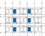
도 2 및 도 3에서 정극성 데이터 전압은 '+'로 표기하고, 부극성 데이터 전압은 '-'로 표기하였다. 그리고 이하에서는 홀수번째 데이터 라인에는 정극성 데이터 전압(+)이 인가되고, 짝수번째 데이터 라인에는 부극성 데이터 전압(-)이 인가되는 특정 프레임만을 예를 들어 설명한다.In FIGS. 2 and 3, the positive data voltage is denoted by '+' and the negative data voltage is denoted by '-'. Hereinafter, a specific frame in which the positive data voltage (+) is applied to the odd-numbered data lines and the negative data voltage (-) is applied to the even-numbered data lines will be described as an example.
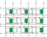
도 2를 참조하면, 서브픽셀들은 제1 내지 제4색을 갖고서 스트라이프 형태로 배열된다. 그리고 서브픽셀들은 2개의 데이터 라인 사이에 2열씩 배열된다.Referring to FIG. 2, subpixels are arranged in a stripe form with first through fourth colors. And the subpixels are arranged in two rows between the two data lines.
여기서, 제1 색은 적색(R)이고, 제2 색은 녹색(G)이고, 제3 색은 청색(B)이고, 제4 색은 백색(W)일 수 있다. 단, 제1 내지 제4 색은 RGBW에 국한되는 것은 아니나, 이하에서는 설명의 편의를 위해 제1 내지 제4 색이 RGBW인 것으로 설명한다.Here, the first color may be red (R), the second color may be green (G), the third color may be blue (B), and the fourth color may be white (W). However, although the first to fourth colors are not limited to RGBW, the first to fourth colors will be described as RGBW for convenience of explanation.
한편, 액정 패널(10)은 RGBW 서브픽셀의 조합으로 구성된 제1 및 제2 화소(P1, P2)를 구비한다. 제1 및 제2 화소(P1, P2)는 열방향으로 번갈아가며 배열됨과 아울러 행방향으로 번갈아가며 배열된다.On the other hand, the
제1 화소(P1)는 제1 내지 제4 서브픽셀(sp1~sp4)을 구비한다.The first pixel P1 includes first through fourth sub-pixels sp1 through sp4.
제1 서브픽셀(sp1)은 좌측 홀수번째 데이터 라인(D1, D3, D5, …)과 짝수번째 게이트 라인(G2, G4, G6, …)에 접속되고 적색(R)을 갖는다. 제2 서브픽셀(sp2)은 우측 짝수번째 데이터 라인(D2, D4, D6, …)과 홀수번째 게이트 라인(G1, G3, G5, …)에 접속되고 녹색(G)을 갖는다. 제3 서브픽셀(sp3)은 좌측 짝수번째 데이터 라인(D2, D4, D6, …)과 짝수번째 게이트 라인(G2, G4, G6, …)에 접속되고 청색(B)을 갖는다. 제4 서브픽셀(sp4)은 우측 홀수번째 데이터 라인(D3, D5, …)과 홀수번째 게이트 라인(G1, G3, G5, …)에 접속되고 백색(W)을 갖는다.The first sub-pixel sp1 is connected to the left odd-numbered data lines D1, D3, D5, ... and the even-numbered gate lines G2, G4, G6, ... and has red (R). The second sub-pixel sp2 is connected to the even-numbered data lines D2, D4, D6, ... and the odd-numbered gate lines G1, G3, G5, ... and has green (G). The third sub-pixel sp3 is connected to the even-numbered data lines D2, D4, D6, ... and the even-numbered gate lines G2, G4, G6, ... and has blue (B). The fourth sub-pixel sp4 is connected to the odd-numbered gate lines G1, G3, G5, ... and the odd-numbered data lines D3, D5, ..., and has a white color W.
제2 화소(P2)는 제5 내지 제8 서브픽셀(sp5~sp8)을 구비한다.And the second pixel P2 includes the fifth to eighth sub-pixels sp5 to sp8.
제5 서브픽셀(sp5)은 우측 짝수번째 데이터 라인(D2, D4, D6, …)과 홀수번째 게이트 라인(G1, G3, G5, …)에 접속되고 적색(R)을 갖는다. 제6 서브픽셀(sp6)은 좌측 홀수번째 데이터 라인(D1, D3, D5, …)과 짝수번째 게이트 라인(G2, G4, G6, …)에 접속되고 녹색(G)을 갖는다. 제7 서브픽셀(sp7)은 우측 홀수번째 데이터 라인(D3, D5, …)과 홀수번째 게이트 라인(G1, G3, G5, …)에 접속되고 청색(B)을 갖는다. 제8 서브픽셀(sp8)은 좌측 짝수번째 데이터 라인(D2, D4, D6, …)과 짝수번째 게이트 라인(G2, G4, G6, …)에 접속되고 백색(W)을 갖는다.The fifth sub-pixel sp5 is connected to the even-numbered data lines D2, D4, D6, ... and the odd-numbered gate lines G1, G3, G5, ... and has red (R). The sixth subpixel sp6 is connected to the left odd-numbered data lines D1, D3, D5, ... and the even-numbered gate lines G2, G4, G6, ... and has green (G). The seventh subpixel sp7 is connected to the odd-numbered gate lines G1, G3, G5, ... and the odd-numbered data lines D3, D5, ..., and has a blue color B. The eighth sub-pixel sp8 is connected to the even-numbered data lines D2, D4, D6, ... and the even-numbered gate lines G2, G4, G6, ... and has a white color W.
이하, 제1 및 제2 화소(P1, P2)의 구동 방법을 도 3을 참조하여 설명한다. 도 3에서 화살표는 데이터 전압이 인가되는 순서를 나타낸다.Hereinafter, a method of driving the first and second pixels P1 and P2 will be described with reference to FIG. In Fig. 3, arrows indicate the order in which the data voltages are applied.
제1 화소(P1)는 홀수번째 게이트 라인(G1, G3, G5, …)으로부터 제공된 스캔 펄스에 응답하여 제2 및 제4 서브픽셀(sp2, sp4)에 데이터 전압이 공급된다. 구체적으로, 제2 서브픽셀(sp2)은 홀수번째 게이트 라인(G1, G3, G5, …)으로부터 제공된 스캔 펄스에 응답하여 우측 짝수번째 데이터 라인(D2, D4, D6, …)으로부터 부극성 데이터 전압(-)이 공급된다. 그리고 제4 서브픽셀(sp4)은 홀수번째 게이트 라인(G1, G3, G5, …)으로부터 제공된 스캔 펄스에 응답하여 우측 홀수번째 데이터 라인(D3, D5, …)으로부터 정극성 데이터 전압(+)이 공급된다.The first pixel P1 is supplied with the data voltage to the second and fourth sub-pixels sp2 and sp4 in response to the scan pulse supplied from the odd gate lines G1, G3, G5,. In detail, the second sub-pixel sp2 receives the negative polarity data voltage V2 from the right-side even-numbered data lines D2, D4, D6, ... in response to the scan pulse supplied from the odd gate lines G1, G3, G5, (-) is supplied. The fourth sub-pixel sp4 receives positive polarity data voltages (+) from the odd-numbered right data lines D3, D5, ... in response to the scan pulses supplied from the odd-numbered gate lines G1, G3, G5, .
이어서, 제1 화소(P1)는 짝수번째 게이트 라인(G2, G4, G6, …)으로부터 제공된 스캔 펄스에 응답하여 제1 및 제3 서브픽셀(sp1, sp3)에 데이터 전압이 공급된다. 구체적으로, 제1 서브픽셀(sp1)은 짝수번째 게이트 라인(G2, G4, G6, …)으로부터 제공된 스캔 펄스에 응답하여 좌측 홀수번째 데이터 라인(D1, D3, D5, …)으로부터 정극성 데이터 전압(+)이 공급된다. 그리고 제3 서브픽셀(sp3)은 짝수번째 게이트 라인(G2, G4, G6, …)으로부터 제공된 스캔 펄스에 응답하여 좌측 짝수번째 데이터 라인(D2, D4, D6, …)으로부터 부극성 데이터 전압(-)이 공급된다.The first pixel P1 is supplied with the data voltage to the first and third sub-pixels sp1 and sp3 in response to the scan pulse supplied from the even-numbered gate lines G2, G4, G6, .... Specifically, the first sub-pixel sp1 receives the positive polarity data voltage V1 from the left odd-numbered data lines D1, D3, D5, ... in response to the scan pulses provided from the even-numbered gate lines G2, G4, G6, (+) Is supplied. The third sub-pixel sp3 is supplied with the negative data voltage (-) from the even-numbered data lines D2, D4, D6, ... in response to the scan pulses provided from the even-numbered gate lines G2, G4, G6, Is supplied.
제2 화소(P2)는 홀수번째 게이트 라인(G1, G3, G5, …)으로부터 제공된 스캔 펄스에 응답하여 제5 및 제7 서브픽셀(sp5, sp7)에 데이터 전압이 공급된다. 구체적으로, 제5 서브픽셀(sp5)은 홀수번째 게이트 라인(G1, G3, G5, …)으로부터 제공된 스캔 펄스에 응답하여 우측 짝수번째 데이터 라인(D2, D4, D6, …)으로부터 부극성 데이터 전압(-)이 공급된다. 그리고 제7 서브픽셀(sp7)은 홀수번째 게이트 라인(G1, G3, G5, …)으로부터 제공된 스캔 펄스에 응답하여 우측 홀수번째 데이터 라인(D3, D5, …)으로부터 정극성 데이터 전압(+)이 공급된다.The second pixel P2 is supplied with the data voltage to the fifth and seventh sub-pixels sp5 and sp7 in response to the scan pulse supplied from the odd gate lines G1, G3, G5, .... Specifically, the fifth sub-pixel sp5 receives the negative data voltages D2, D4, D6, ... from the even-numbered data lines D2, D4, D6, ... in response to the scan pulses provided from the odd gate lines G1, G3, G5, (-) is supplied. The seventh sub-pixel sp7 receives positive polarity data voltages (+) from the odd-numbered right data lines D3, D5, ... in response to the scan pulses supplied from the odd-numbered gate lines G1, G3, G5, .
이어서, 제2 화소(P2)는 짝수번째 게이트 라인(G2, G4, G6, …)으로부터 제공된 스캔 펄스에 응답하여 제6 및 제8 서브픽셀(sp6, sp8)에 데이터 전압이 공급된다. 구체적으로, 제6 서브픽셀(sp6)은 짝수번째 게이트 라인(G2, G4, G6, …)으로부터 제공된 스캔 펄스에 응답하여 좌측 홀수번째 데이터 라인(D1, D3, D5, …)으로부터 정극성 데이터 전압(+)이 공급된다. 그리고 제8 서브픽셀(sp8)은 짝수번째 게이트 라인(G2, G4, G6, …)으로부터 제공된 스캔 펄스에 응답하여 좌측 짝수번째 데이터 라인(D2, D4, D6, …)으로부터 부극성 데이터 전압(-)이 공급된다.Then, the second pixel P2 is supplied with the data voltage to the sixth and eighth sub-pixels sp6 and sp8 in response to the scan pulse provided from the even-numbered gate lines G2, G4, G6, .... Specifically, the sixth sub-pixel sp6 is supplied with the positive polarity data voltage V1 from the left odd-numbered data lines D1, D3, D5, ... in response to the scan pulses provided from the even-numbered gate lines G2, G4, G6, (+) Is supplied. The eighth sub-pixel sp8 is supplied with the negative data voltage (-) from the even-numbered data lines D2, D4, D6, ... in response to the scan pulses provided from the even-numbered gate lines G2, G4, G6, Is supplied.
도 4a 내지 도 4c는 실시 예에 따른 액정 패널(10)이 단색 패턴을 표시할 경우를 나타낸 평면도이다.4A to 4C are plan views showing a case where the
도 4a를 참조하면, 적색(R) 패턴을 표시할 경우, 적색(R)을 갖는 서브픽셀들(sp1, sp5)에 정극성 데이터 전압(+)과 부극성 데이터 전압(+)이 행방향과 열방향으로 번갈아가며 공급되는 것을 알 수 있고, 도 4b를 참조하면, 녹색(G) 패턴을 표시할 경우, 녹색(G)을 갖는 서브픽셀들(sp2, sp6)에 정극성 데이터 전압(+)과 부극성 데이터 전압(+)이 행방향과 열방향으로 번갈아가며 공급되는 것을 알 수 있고, 도 4c를 참조하면 청색(B) 패턴을 표시할 경우, 청색(B)을 갖는 서브픽셀들(sp3, sp7)에 정극성 데이터 전압(+)과 부극성 데이터 전압(+)이 행방향과 열방향으로 번갈아가며 공급되는 것을 알 수 있다.4A, when a red (R) pattern is displayed, a positive data voltage (+) and a negative data voltage (+) are applied to the subpixels sp1 and sp5 having red (R) Referring to FIG. 4B, when a green (G) pattern is displayed, positive polarity data voltages (+) are applied to the sub-pixels sp2 and sp6 having green (G) Referring to FIG. 4C, when a blue (B) pattern is displayed, the subpixels sp3 (blue) having blue (B) are alternately supplied in the row direction and the column direction. (+) and the negative data voltage (+) are alternately supplied in the row direction and the column direction, respectively.
따라서, 실시 예는 단색 패턴을 표시할 경우 수직 방향 또는 수평 방향으로 동일 극성의 데이터 전압이 인가되는 것을 방지하고, 수직 방향 또는 수평 방향의 라인 딤을 방지하여 화질이 향상된다.Therefore, in the embodiment, when a monochromatic pattern is displayed, it is prevented that the data voltage of the same polarity is applied in the vertical direction or the horizontal direction, and the line dim in the vertical direction or the horizontal direction is prevented.
이상에서 설명한 본 발명은 상술한 실시 예 및 첨부된 도면에 한정되는 것이 아니고, 본 발명의 기술적 사상을 벗어나지 않는 범위 내에서 여러 가지 치환, 변형 및 변경이 가능하다는 것이 본 발명이 속하는 기술분야에서 통상의 지식을 가진 자에게 있어 명백할 것이다.It will be apparent to those skilled in the art that various modifications and variations can be made in the present invention without departing from the spirit or scope of the general inventive concept as defined by the appended claims and their equivalents. Will be clear to those who have knowledge of.
10: 액정패널11: 타이밍 제어부
12: 데이터 구동회로14: 게이트 구동회로10: liquid crystal panel 11: timing controller
12: Data driving circuit 14: Gate driving circuit
Claims (10)
Translated fromKorean상기 서브픽셀들은 제1 내지 제4 색을 갖고서 스트라이프 형태로 배열되고;
제1 및 제2 게이트 라인 사이에 제1 내지 제4 서브픽셀로 구성된 제1 화소와, 제5 내지 제8 서브픽셀로 구성된 제2화소가 배열되되, 상기 제1 및 제2 서브픽셀은 제1 및 제2 데이터 라인 사이에 배열되고, 상기 제3 및 제4 서브픽셀은 상기 제2 및 제3 데이터 라인 사이에 배열되고, 상기 제5 및 제6 서브픽셀은 상기 제3 및 제4 데이터 라인 사이에 배열되고, 상기 제7 및 제8 서브픽셀은 상기 제4 및 제5 데이터 라인 사이에 배열되고;
상기 제1 서브픽셀은 상기 제1 데이터 라인에 접속되고, 상기 제2 및 제3 서브픽셀은 상기 제2 데이터 라인에 접속되고, 상기 제4 및 제6 서브픽셀은 상기 제3 데이터 라인에 접속되고, 상기 제5 및 제8 서브픽셀은 상기 제4 데이터 라인에 접속되고, 상기 제7 서브픽셀은 상기 제5 데이터 라인에 접속되며;
상기 제1 및 제2 화소가 열방향으로 번갈아가며 배열됨과 아울러 행방향으로 번갈아가며 배열되는 것을 특징으로 하는 액정 표시 장치.defining mxn subpixels intersecting m / 2 data lines and 2n gate lines;
The subpixels are arranged in a stripe shape with first to fourth colors;
A first pixel composed of first through fourth sub-pixels and a second pixel composed of fifth through eighth sub-pixels are arranged between the first and second gate lines, the first and second sub- And the third and fourth subpixels are arranged between the second and third data lines and the fifth and sixth subpixels are arranged between the third and fourth data lines, And the seventh and eighth subpixels are arranged between the fourth and fifth data lines;
The first and second subpixels are connected to the first data line, the second and third subpixels are connected to the second data line, the fourth and sixth subpixels are connected to the third data line The fifth and eighth subpixels are connected to the fourth data line, and the seventh subpixel is connected to the fifth data line;
Wherein the first and second pixels are alternately arranged in the column direction and are alternately arranged in the row direction.
상기 제1 및 제5 서브픽셀은 상기 제1 색을 갖고, 상기 제2 및 제6 서브픽셀은 상기 제2 색을 갖고, 상기 제3 및 제7 서브픽셀은 상기 제3 색을 갖고, 상기 제4 및 제8 서브픽셀은 상기 제4 색을 갖는 것을 특징으로 하는 액정 표시 장치.The method according to claim 1,
Wherein the first and fifth sub-pixels have the first color, the second and sixth sub-pixels have the second color, the third and seventh sub-pixels have the third color, 4 and the eighth sub-pixel have the fourth color.
1프레임 기간 동안 인접한 데이터 라인에 서로 다른 극성의 데이터 전압이 인가되는 것을 특징으로 하는 액정 표시 장치.The method according to claim 1,
And data voltages having different polarities are applied to adjacent data lines during one frame period.
상기 제2, 제4, 제5, 제7 서브픽셀은 상기 제1 게이트 라인에 접속되고, 상기 제1, 제3, 제6, 제8 서브픽셀은 상기 제2 게이트 라인에 접속되는 것을 특징으로 하는 액정 표시 장치.The method according to claim 1,
Pixels are connected to the first gate line, and the first, third, sixth, and eighth sub-pixels are connected to the second gate line. .
상기 제1 색은 적색이고, 상기 제2 색은 녹색이고, 상기 제3 색은 청색이고, 상기 제4 색은 백색인 것을 특징으로 하는 액정 표시 장치.The method according to claim 1,
Wherein the first color is red, the second color is green, the third color is blue, and the fourth color is white.
상기 m×n개의 서브픽셀을 구동하는 단계는 제1 및 제2 게이트 라인 사이에 제1 내지 제4 서브픽셀로 구성된 제1 화소를 구동하는 단계와, 상기 제1 및 제2 게이트 라인 사이에 제5 및 제8 서브픽셀로 구성된 제2 화소를 구동하는 단계를 포함하고;
상기 제1 및 제2 서브픽셀은 제1 및 제2 데이터 라인 사이에 배열되고, 상기 제3 및 제4 서브픽셀은 상기 제2 및 제3 데이터 라인 사이에 배열되고, 상기 제5 및 제6 서브픽셀은 상기 제3 및 제4 데이터 라인 사이에 배열되고, 상기 제7 및 제8 서브픽셀은 상기 제4 및 제5 데이터 라인 사이에 배열되고;
상기 제1 서브픽셀은 상기 제1 데이터 라인에 접속되고, 상기 제2 및 제3 서브픽셀은 상기 제2 데이터 라인에 접속되고, 상기 제4 및 제6 서브픽셀은 상기 제3 데이터 라인에 접속되고, 상기 제5 및 제8 서브픽셀은 상기 제4 데이터 라인에 접속되고, 상기 제7 서브픽셀은 상기 제5 데이터 라인에 접속되며;
상기 제1 및 제2 화소가 열방향으로 번갈아가며 배열됨과 아울러 행방향으로 번갈아가며 배열되는 것을 특징으로 하는 액정 표시 장치의 구동 방법.The scan lines are sequentially supplied to the 2n gate lines and the data voltages are supplied to m / 2 data lines in synchronization with the scan pulses, and the data lines are arranged in two rows between the two data lines, And driving m x n subpixels arranged in a stripe form;
Wherein driving the mxn subpixels comprises driving a first pixel comprised of first through fourth subpixels between first and second gate lines, driving a first pixel comprised of first through fourth subpixels between the first and second gate lines, 5 and an eighth sub-pixel;
Wherein the first and second subpixels are arranged between first and second data lines, the third and fourth subpixels are arranged between the second and third data lines, the fifth and sixth subpixels are arranged between the first and second data lines, Pixels are arranged between the third and fourth data lines, the seventh and eighth sub-pixels are arranged between the fourth and fifth data lines;
The first and second subpixels are connected to the first data line, the second and third subpixels are connected to the second data line, the fourth and sixth subpixels are connected to the third data line The fifth and eighth subpixels are connected to the fourth data line, and the seventh subpixel is connected to the fifth data line;
Wherein the first and second pixels are alternately arranged in the column direction and are alternately arranged in the row direction.
상기 제1 및 제5 서브픽셀은 상기 제1 색을 갖고, 상기 제2 및 제6 서브픽셀은 상기 제2 색을 갖고, 상기 제3 및 제7 서브픽셀은 상기 제3 색을 갖고, 상기 제4 및 제8 서브픽셀은 상기 제4 색을 갖는 것을 특징으로 하는 액정 표시 장치의 구동 방법.The method of claim 6,
Wherein the first and fifth sub-pixels have the first color, the second and sixth sub-pixels have the second color, the third and seventh sub-pixels have the third color, 4 and the eighth sub-pixel have the fourth color.
m/2개의 데이터 라인에 데이터 전압을 공급하는 단계는
1프레임 기간 동안 인접한 데이터 라인에 서로 다른 극성의 데이터 전압을 공급하는 단계인 것을 특징으로 하는 액정 표시 장치의 구동 방법.The method of claim 6,
The step of supplying the data voltage to the m / 2 data lines
And supplying data voltages having different polarities to adjacent data lines during one frame period.
상기 제1 색은 적색이고, 상기 제2 색은 녹색이고, 상기 제3 색은 청색이고, 상기 제4 색은 백색인 것을 특징으로 하는 액정 표시 장치의 구동 방법.The method of claim 6,
Wherein the first color is red, the second color is green, the third color is blue, and the fourth color is white.
상기 제1 화소를 구동하는 단계는
상기 제1 게이트 라인으로부터 제공된 스캔 펄스에 응답하여 상기 제2 및 제4 서브픽셀에 각각 제2 극성의 데이터 전압과 제1 극성의 데이터 전압을 공급하고, 이어서 상기 제2 게이트 라인으로부터 제공된 스캔 펄스에 응답하여 상기 제1 및 제3 서브픽셀에 각각 상기 제1 극성의 데이터 전압과 상기 제2 극성의 데이터 전압을 공급하는 단계를 포함하고;
상기 제2 화소를 구동하는 단계는
상기 제1 게이트 라인으로부터 제공된 스캔 펄스에 응답하여 상기 제5 및 제7 서브픽셀에 각각 상기 제2 극성의 데이터 전압과 상기 제1 극성의 데이터 전압을 공급하고, 이어서 제2 게이트 라인으로부터 제공된 스캔 펄스에 응답하여 상기 제6 및 제8 서브픽셀에 각각 상기 제1 극성의 데이터 전압과 상기 제2 극성의 데이터 전압을 공급하는 단계를 포함하는 것을 특징으로 하는 액정 표시 장치의 구동 방법.The method of claim 6,
The step of driving the first pixel
Supplying a data voltage of a second polarity and a data voltage of a first polarity to the second and fourth subpixels in response to a scan pulse provided from the first gate line, And supplying a data voltage of the first polarity and a data voltage of the second polarity to the first and third subpixels, respectively, in response to the first polarity data voltage and the second polarity data voltage;
The step of driving the second pixel
Supplying a data voltage of the second polarity and a data voltage of the first polarity to the fifth and seventh subpixels in response to a scan pulse provided from the first gate line, And supplying the data voltage of the first polarity and the data voltage of the second polarity to the sixth and eighth sub-pixels, respectively.
Priority Applications (3)
| Application Number | Priority Date | Filing Date | Title |
|---|---|---|---|
| KR1020120125037AKR20140058252A (en) | 2012-11-06 | 2012-11-06 | Liquid crystal display device and driving method the same |
| US14/069,596US20140125647A1 (en) | 2012-11-06 | 2013-11-01 | Liquid crystal display device and method of driving the same |
| CN201310540935.4ACN103809313A (en) | 2012-11-06 | 2013-11-05 | Liquid crystal display device and method of driving the same |
Applications Claiming Priority (1)
| Application Number | Priority Date | Filing Date | Title |
|---|---|---|---|
| KR1020120125037AKR20140058252A (en) | 2012-11-06 | 2012-11-06 | Liquid crystal display device and driving method the same |
Publications (1)
| Publication Number | Publication Date |
|---|---|
| KR20140058252Atrue KR20140058252A (en) | 2014-05-14 |
Family
ID=50621916
Family Applications (1)
| Application Number | Title | Priority Date | Filing Date |
|---|---|---|---|
| KR1020120125037AWithdrawnKR20140058252A (en) | 2012-11-06 | 2012-11-06 | Liquid crystal display device and driving method the same |
Country Status (3)
| Country | Link |
|---|---|
| US (1) | US20140125647A1 (en) |
| KR (1) | KR20140058252A (en) |
| CN (1) | CN103809313A (en) |
Cited By (3)
| Publication number | Priority date | Publication date | Assignee | Title |
|---|---|---|---|---|
| KR20170041312A (en)* | 2015-10-06 | 2017-04-17 | 엘지디스플레이 주식회사 | Liquid crystal display device |
| US9978301B2 (en) | 2015-12-28 | 2018-05-22 | Samsung Display Co., Ltd. | Display apparatus |
| US10210825B2 (en)* | 2015-03-26 | 2019-02-19 | Japan Display Inc. | Display device |
Families Citing this family (21)
| Publication number | Priority date | Publication date | Assignee | Title |
|---|---|---|---|---|
| US10147371B2 (en) | 2014-06-27 | 2018-12-04 | Lg Display Co., Ltd. | Display device having pixels with shared data lines |
| CN104062792B (en)* | 2014-07-04 | 2017-06-30 | 深圳市华星光电技术有限公司 | A kind of method and device for driving HSD liquid crystal display panels |
| KR102263258B1 (en)* | 2014-08-25 | 2021-06-10 | 삼성디스플레이 주식회사 | Organic Light Emitting Display Device and Driving Method Thereof |
| CN104252854A (en)* | 2014-09-28 | 2014-12-31 | 京东方科技集团股份有限公司 | Array substrate, driving method thereof, display panel and display device |
| US9341905B1 (en)* | 2014-11-10 | 2016-05-17 | Shenzhen China Star Optoelectronics Technology Co., Ltd | Array substrate, liquid crystal display panel and liquid crystal display |
| CN104298041B (en)* | 2014-11-10 | 2017-04-26 | 深圳市华星光电技术有限公司 | Array substrate, liquid crystal display panel and liquid crystal display |
| CN104360551B (en)* | 2014-11-10 | 2017-02-15 | 深圳市华星光电技术有限公司 | Array substrate, liquid crystal panel and liquid crystal display |
| TWI556048B (en) | 2014-12-02 | 2016-11-01 | 聯詠科技股份有限公司 | Display device and driving module thereof |
| CN105739140B (en)* | 2014-12-10 | 2019-05-24 | 联咏科技股份有限公司 | display device and driving module thereof |
| CN104460153A (en)* | 2014-12-12 | 2015-03-25 | 深圳市华星光电技术有限公司 | Liquid crystal display and array substrate thereof |
| KR102299951B1 (en)* | 2015-01-08 | 2021-09-08 | 삼성디스플레이 주식회사 | Liquid Display Device |
| KR102342685B1 (en)* | 2015-03-05 | 2021-12-24 | 삼성디스플레이 주식회사 | Display panel and display apparatus having the same |
| KR102296920B1 (en)* | 2015-03-13 | 2021-09-02 | 삼성디스플레이 주식회사 | Display device |
| CN104730793B (en)* | 2015-04-15 | 2018-03-20 | 合肥京东方光电科技有限公司 | Dot structure and its driving method, display panel and display device |
| KR102349500B1 (en)* | 2015-04-21 | 2022-01-12 | 엘지디스플레이 주식회사 | Liquid crystal display device |
| CN105093737A (en)* | 2015-07-28 | 2015-11-25 | 深圳市华星光电技术有限公司 | Liquid crystal display |
| CN105319793B (en) | 2015-11-26 | 2019-09-24 | 深圳市华星光电技术有限公司 | Array substrate with data line share framework |
| KR102484230B1 (en)* | 2015-12-22 | 2023-01-03 | 삼성디스플레이 주식회사 | Liquid crystal display device |
| CN106292110A (en)* | 2016-09-23 | 2017-01-04 | 京东方科技集团股份有限公司 | A kind of array base palte, display floater, display device |
| US10504463B2 (en)* | 2017-03-13 | 2019-12-10 | Synaptics Incorporated | Display panel with reduced source lines |
| KR20230139885A (en)* | 2022-03-24 | 2023-10-06 | 삼성디스플레이 주식회사 | Display device |
Family Cites Families (5)
| Publication number | Priority date | Publication date | Assignee | Title |
|---|---|---|---|---|
| JP2004240192A (en)* | 2003-02-06 | 2004-08-26 | Seiko Epson Corp | Electro-optical panel and driving method thereof, electro-optical device, and electronic apparatus |
| US8648889B2 (en)* | 2005-11-30 | 2014-02-11 | Sharp Kabushiki Kaisha | Display device and method for driving display member |
| KR101309552B1 (en)* | 2006-11-01 | 2013-09-23 | 삼성디스플레이 주식회사 | Array substrate and display panel having the same |
| CN101846859A (en)* | 2009-03-25 | 2010-09-29 | 友达光电股份有限公司 | Liquid crystal display device having a plurality of pixel electrodes |
| KR101695018B1 (en)* | 2009-12-07 | 2017-01-10 | 엘지디스플레이 주식회사 | Liquid crystal display |
- 2012
- 2012-11-06KRKR1020120125037Apatent/KR20140058252A/ennot_activeWithdrawn
- 2013
- 2013-11-01USUS14/069,596patent/US20140125647A1/ennot_activeAbandoned
- 2013-11-05CNCN201310540935.4Apatent/CN103809313A/enactivePending
Cited By (3)
| Publication number | Priority date | Publication date | Assignee | Title |
|---|---|---|---|---|
| US10210825B2 (en)* | 2015-03-26 | 2019-02-19 | Japan Display Inc. | Display device |
| KR20170041312A (en)* | 2015-10-06 | 2017-04-17 | 엘지디스플레이 주식회사 | Liquid crystal display device |
| US9978301B2 (en) | 2015-12-28 | 2018-05-22 | Samsung Display Co., Ltd. | Display apparatus |
Also Published As
| Publication number | Publication date |
|---|---|
| US20140125647A1 (en) | 2014-05-08 |
| CN103809313A (en) | 2014-05-21 |
Similar Documents
| Publication | Publication Date | Title |
|---|---|---|
| KR20140058252A (en) | Liquid crystal display device and driving method the same | |
| KR101441395B1 (en) | Liquid crystal display device and driving method the same | |
| KR101782054B1 (en) | Liquid crystal display device and driving method thereof | |
| US8970564B2 (en) | Apparatus and method for driving liquid crystal display | |
| CN106067293B (en) | LCD Monitor | |
| KR102306598B1 (en) | Display apparatus | |
| US9099054B2 (en) | Liquid crystal display and driving method thereof | |
| KR102063346B1 (en) | Liquid crystal display | |
| US20180114495A1 (en) | Display panel, liquid crystal display and driving method therefor | |
| US9978322B2 (en) | Display apparatus | |
| KR102113621B1 (en) | Liquid crystal display device | |
| KR102360758B1 (en) | Display device | |
| US9865203B2 (en) | Display apparatus and method of driving the same | |
| KR102134320B1 (en) | Liquid crystal display | |
| US10043463B2 (en) | Display apparatus and method of driving the same | |
| KR101830241B1 (en) | liquid crystal display device and method of driving the same | |
| KR102279815B1 (en) | Liquid crystal display device and driving method thereof | |
| KR101985245B1 (en) | Liquid crystal display | |
| KR20130020308A (en) | Method of driving liquid crystal panel | |
| KR102244985B1 (en) | Display panel | |
| KR101989829B1 (en) | Liquid crystal display device and method for driving the same | |
| KR20100077434A (en) | Liquid crystal display and driving method thereof | |
| KR20170000883A (en) | Display device |
Legal Events
| Date | Code | Title | Description |
|---|---|---|---|
| PA0109 | Patent application | Patent event code:PA01091R01D Comment text:Patent Application Patent event date:20121106 | |
| PG1501 | Laying open of application | ||
| PC1203 | Withdrawal of no request for examination | ||
| WITN | Application deemed withdrawn, e.g. because no request for examination was filed or no examination fee was paid |