KR20140056929A - Light emitting device - Google Patents
Light emitting deviceDownload PDFInfo
- Publication number
- KR20140056929A KR20140056929AKR1020120123414AKR20120123414AKR20140056929AKR 20140056929 AKR20140056929 AKR 20140056929AKR 1020120123414 AKR1020120123414 AKR 1020120123414AKR 20120123414 AKR20120123414 AKR 20120123414AKR 20140056929 AKR20140056929 AKR 20140056929A
- Authority
- KR
- South Korea
- Prior art keywords
- layer
- light emitting
- region
- electron blocking
- well
- Prior art date
- Legal status (The legal status is an assumption and is not a legal conclusion. Google has not performed a legal analysis and makes no representation as to the accuracy of the status listed.)
- Ceased
Links
- 239000004065semiconductorSubstances0.000claimsabstractdescription151
- 230000000903blocking effectEffects0.000claimsabstractdescription110
- 230000004888barrier functionEffects0.000claimsabstractdescription101
- 238000002347injectionMethods0.000claimsdescription58
- 239000007924injectionSubstances0.000claimsdescription58
- 238000000034methodMethods0.000claimsdescription37
- 230000007423decreaseEffects0.000claimsdescription20
- 239000000463materialSubstances0.000description28
- 239000000758substrateSubstances0.000description27
- XLOMVQKBTHCTTD-UHFFFAOYSA-NZinc monoxideChemical compound[Zn]=OXLOMVQKBTHCTTD-UHFFFAOYSA-N0.000description24
- 239000002019doping agentSubstances0.000description24
- 238000010586diagramMethods0.000description15
- OAICVXFJPJFONN-UHFFFAOYSA-NPhosphorusChemical compound[P]OAICVXFJPJFONN-UHFFFAOYSA-N0.000description12
- 239000011787zinc oxideSubstances0.000description12
- PXHVJJICTQNCMI-UHFFFAOYSA-NnickelSubstances[Ni]PXHVJJICTQNCMI-UHFFFAOYSA-N0.000description11
- 239000000203mixtureSubstances0.000description10
- 238000005530etchingMethods0.000description8
- 229910052738indiumInorganic materials0.000description8
- 239000004973liquid crystal related substanceSubstances0.000description8
- 229910052733galliumInorganic materials0.000description7
- 229910052751metalInorganic materials0.000description7
- 239000002184metalSubstances0.000description7
- 229910052759nickelInorganic materials0.000description7
- 238000002161passivationMethods0.000description7
- GYHNNYVSQQEPJS-UHFFFAOYSA-NGalliumChemical compound[Ga]GYHNNYVSQQEPJS-UHFFFAOYSA-N0.000description6
- 238000005229chemical vapour depositionMethods0.000description6
- 150000001875compoundsChemical class0.000description6
- JAONJTDQXUSBGG-UHFFFAOYSA-Ndialuminum;dizinc;oxygen(2-)Chemical compound[O-2].[O-2].[O-2].[O-2].[O-2].[Al+3].[Al+3].[Zn+2].[Zn+2]JAONJTDQXUSBGG-UHFFFAOYSA-N0.000description6
- 229910052737goldInorganic materials0.000description6
- 238000004519manufacturing processMethods0.000description6
- SKRWFPLZQAAQSU-UHFFFAOYSA-Nstibanylidynetin;hydrateChemical compoundO.[Sn].[Sb]SKRWFPLZQAAQSU-UHFFFAOYSA-N0.000description6
- 230000008859changeEffects0.000description5
- 229910052804chromiumInorganic materials0.000description5
- 239000010949copperSubstances0.000description5
- APFVFJFRJDLVQX-UHFFFAOYSA-Nindium atomChemical compound[In]APFVFJFRJDLVQX-UHFFFAOYSA-N0.000description5
- VRIVJOXICYMTAG-IYEMJOQQSA-Liron(ii) gluconateChemical compound[Fe+2].OC[C@@H](O)[C@@H](O)[C@H](O)[C@@H](O)C([O-])=O.OC[C@@H](O)[C@@H](O)[C@H](O)[C@@H](O)C([O-])=OVRIVJOXICYMTAG-IYEMJOQQSA-L0.000description5
- 230000008569processEffects0.000description5
- 229910052718tinInorganic materials0.000description5
- 229910052719titaniumInorganic materials0.000description5
- 229910019897RuOxInorganic materials0.000description4
- VYPSYNLAJGMNEJ-UHFFFAOYSA-NSilicium dioxideChemical compoundO=[Si]=OVYPSYNLAJGMNEJ-UHFFFAOYSA-N0.000description4
- 229910052732germaniumInorganic materials0.000description4
- 238000002248hydride vapour-phase epitaxyMethods0.000description4
- 238000000465mouldingMethods0.000description4
- 238000000623plasma-assisted chemical vapour depositionMethods0.000description4
- 229910052710siliconInorganic materials0.000description4
- 229910052709silverInorganic materials0.000description4
- 229910052725zincInorganic materials0.000description4
- 239000011701zincSubstances0.000description4
- IJGRMHOSHXDMSA-UHFFFAOYSA-NAtomic nitrogenChemical compoundN#NIJGRMHOSHXDMSA-UHFFFAOYSA-N0.000description3
- 229910001218Gallium arsenideInorganic materials0.000description3
- 229910052788bariumInorganic materials0.000description3
- 229910052791calciumInorganic materials0.000description3
- 229910052802copperInorganic materials0.000description3
- 238000009792diffusion processMethods0.000description3
- YZZNJYQZJKSEER-UHFFFAOYSA-Ngallium tinChemical compound[Ga].[Sn]YZZNJYQZJKSEER-UHFFFAOYSA-N0.000description3
- AMGQUBHHOARCQH-UHFFFAOYSA-Nindium;oxotinChemical compound[In].[Sn]=OAMGQUBHHOARCQH-UHFFFAOYSA-N0.000description3
- HRHKULZDDYWVBE-UHFFFAOYSA-Nindium;oxozinc;tinChemical compound[In].[Sn].[Zn]=OHRHKULZDDYWVBE-UHFFFAOYSA-N0.000description3
- 229910052741iridiumInorganic materials0.000description3
- 238000002955isolationMethods0.000description3
- 229910052749magnesiumInorganic materials0.000description3
- 150000004767nitridesChemical class0.000description3
- 230000003287optical effectEffects0.000description3
- 229910052697platinumInorganic materials0.000description3
- 239000010948rhodiumSubstances0.000description3
- 229910052712strontiumInorganic materials0.000description3
- 229910001887tin oxideInorganic materials0.000description3
- WFKWXMTUELFFGS-UHFFFAOYSA-NtungstenChemical compound[W]WFKWXMTUELFFGS-UHFFFAOYSA-N0.000description3
- 229910052721tungstenInorganic materials0.000description3
- 239000010937tungstenSubstances0.000description3
- YVTHLONGBIQYBO-UHFFFAOYSA-Nzinc indium(3+) oxygen(2-)Chemical compound[O--].[Zn++].[In+3]YVTHLONGBIQYBO-UHFFFAOYSA-N0.000description3
- 229910000980Aluminium gallium arsenideInorganic materials0.000description2
- RYGMFSIKBFXOCR-UHFFFAOYSA-NCopperChemical compound[Cu]RYGMFSIKBFXOCR-UHFFFAOYSA-N0.000description2
- 229910005191Ga 2 O 3Inorganic materials0.000description2
- 229910002601GaNInorganic materials0.000description2
- BPQQTUXANYXVAA-UHFFFAOYSA-NOrthosilicateChemical compound[O-][Si]([O-])([O-])[O-]BPQQTUXANYXVAA-UHFFFAOYSA-N0.000description2
- 239000004698PolyethyleneSubstances0.000description2
- 229910052581Si3N4Inorganic materials0.000description2
- 229910000577Silicon-germaniumInorganic materials0.000description2
- GWEVSGVZZGPLCZ-UHFFFAOYSA-NTitan oxideChemical compoundO=[Ti]=OGWEVSGVZZGPLCZ-UHFFFAOYSA-N0.000description2
- 229910052782aluminiumInorganic materials0.000description2
- 239000003086colorantSubstances0.000description2
- 230000000052comparative effectEffects0.000description2
- 238000001312dry etchingMethods0.000description2
- 239000007789gasSubstances0.000description2
- 239000011521glassSubstances0.000description2
- 229910052735hafniumInorganic materials0.000description2
- 238000009616inductively coupled plasmaMethods0.000description2
- 239000007788liquidSubstances0.000description2
- 239000007769metal materialSubstances0.000description2
- 229910003465moissaniteInorganic materials0.000description2
- 238000001451molecular beam epitaxyMethods0.000description2
- 229910052750molybdenumInorganic materials0.000description2
- GNRSAWUEBMWBQH-UHFFFAOYSA-Nnickel(II) oxideInorganic materials[Ni]=OGNRSAWUEBMWBQH-UHFFFAOYSA-N0.000description2
- TWNQGVIAIRXVLR-UHFFFAOYSA-Noxo(oxoalumanyloxy)alumaneChemical compoundO=[Al]O[Al]=OTWNQGVIAIRXVLR-UHFFFAOYSA-N0.000description2
- 229920003229poly(methyl methacrylate)Polymers0.000description2
- 229920000573polyethylenePolymers0.000description2
- -1polyethylene terephthalatePolymers0.000description2
- 229920000139polyethylene terephthalatePolymers0.000description2
- 239000005020polyethylene terephthalateSubstances0.000description2
- 239000004926polymethyl methacrylateSubstances0.000description2
- 229910052703rhodiumInorganic materials0.000description2
- 229910052711seleniumInorganic materials0.000description2
- 229910010271silicon carbideInorganic materials0.000description2
- 229910052814silicon oxideInorganic materials0.000description2
- 229910052714telluriumInorganic materials0.000description2
- 230000005641tunnelingEffects0.000description2
- 229910002704AlGaNInorganic materials0.000description1
- QGZKDVFQNNGYKY-UHFFFAOYSA-NAmmoniaChemical compoundNQGZKDVFQNNGYKY-UHFFFAOYSA-N0.000description1
- 229910000881Cu alloyInorganic materials0.000description1
- 206010027339Menstruation irregularDiseases0.000description1
- ZOKXTWBITQBERF-UHFFFAOYSA-NMolybdenumChemical compound[Mo]ZOKXTWBITQBERF-UHFFFAOYSA-N0.000description1
- 229910004298SiO 2Inorganic materials0.000description1
- 229910004283SiO 4Inorganic materials0.000description1
- 229910020286SiOxNyInorganic materials0.000description1
- XUIMIQQOPSSXEZ-UHFFFAOYSA-NSiliconChemical compound[Si]XUIMIQQOPSSXEZ-UHFFFAOYSA-N0.000description1
- 229910010413TiO 2Inorganic materials0.000description1
- DZLPZFLXRVRDAE-UHFFFAOYSA-N[O--].[O--].[O--].[O--].[Al+3].[Zn++].[In+3]Chemical compound[O--].[O--].[O--].[O--].[Al+3].[Zn++].[In+3]DZLPZFLXRVRDAE-UHFFFAOYSA-N0.000description1
- 230000004913activationEffects0.000description1
- 229910045601alloyInorganic materials0.000description1
- 239000000956alloySubstances0.000description1
- PNEYBMLMFCGWSK-UHFFFAOYSA-Naluminium oxideInorganic materials[O-2].[O-2].[O-2].[Al+3].[Al+3]PNEYBMLMFCGWSK-UHFFFAOYSA-N0.000description1
- 230000005540biological transmissionEffects0.000description1
- 229910052797bismuthInorganic materials0.000description1
- 229910052681coesiteInorganic materials0.000description1
- 238000004891communicationMethods0.000description1
- 239000004020conductorSubstances0.000description1
- SBYXRAKIOMOBFF-UHFFFAOYSA-Ncopper tungstenChemical compound[Cu].[W]SBYXRAKIOMOBFF-UHFFFAOYSA-N0.000description1
- 229910052593corundumInorganic materials0.000description1
- 229910052906cristobaliteInorganic materials0.000description1
- 239000013078crystalSubstances0.000description1
- 230000003247decreasing effectEffects0.000description1
- 230000006866deteriorationEffects0.000description1
- 229910001873dinitrogenInorganic materials0.000description1
- 230000005684electric fieldEffects0.000description1
- 238000005265energy consumptionMethods0.000description1
- 238000000605extractionMethods0.000description1
- 239000002223garnetSubstances0.000description1
- 239000012535impuritySubstances0.000description1
- GKOZUEZYRPOHIO-UHFFFAOYSA-Niridium atomChemical compound[Ir]GKOZUEZYRPOHIO-UHFFFAOYSA-N0.000description1
- 239000011159matrix materialSubstances0.000description1
- 239000011733molybdenumSubstances0.000description1
- 229910052757nitrogenInorganic materials0.000description1
- 229910052763palladiumInorganic materials0.000description1
- 238000007747platingMethods0.000description1
- 230000010287polarizationEffects0.000description1
- 239000004417polycarbonateSubstances0.000description1
- 229920000515polycarbonatePolymers0.000description1
- 229920000642polymerPolymers0.000description1
- 239000002096quantum dotSubstances0.000description1
- 230000004044responseEffects0.000description1
- MHOVAHRLVXNVSD-UHFFFAOYSA-Nrhodium atomChemical compound[Rh]MHOVAHRLVXNVSD-UHFFFAOYSA-N0.000description1
- 239000010703siliconSubstances0.000description1
- 239000000377silicon dioxideSubstances0.000description1
- 235000012239silicon dioxideNutrition0.000description1
- HQVNEWCFYHHQES-UHFFFAOYSA-Nsilicon nitrideChemical compoundN12[Si]34N5[Si]62N3[Si]51N64HQVNEWCFYHHQES-UHFFFAOYSA-N0.000description1
- 239000002210silicon-based materialSubstances0.000description1
- 239000007787solidSubstances0.000description1
- 229910052682stishoviteInorganic materials0.000description1
- 239000000126substanceSubstances0.000description1
- 229920003002synthetic resinPolymers0.000description1
- 239000000057synthetic resinSubstances0.000description1
- 238000002834transmittanceMethods0.000description1
- 229910052905tridymiteInorganic materials0.000description1
- XCZXGTMEAKBVPV-UHFFFAOYSA-NtrimethylgalliumChemical compoundC[Ga](C)CXCZXGTMEAKBVPV-UHFFFAOYSA-N0.000description1
- IBEFSUTVZWZJEL-UHFFFAOYSA-NtrimethylindiumChemical compoundC[In](C)CIBEFSUTVZWZJEL-UHFFFAOYSA-N0.000description1
- 238000007740vapor depositionMethods0.000description1
- 238000001039wet etchingMethods0.000description1
- 229910001845yogo sapphireInorganic materials0.000description1
Images


Classifications
- H—ELECTRICITY
- H10—SEMICONDUCTOR DEVICES; ELECTRIC SOLID-STATE DEVICES NOT OTHERWISE PROVIDED FOR
- H10H—INORGANIC LIGHT-EMITTING SEMICONDUCTOR DEVICES HAVING POTENTIAL BARRIERS
- H10H20/00—Individual inorganic light-emitting semiconductor devices having potential barriers, e.g. light-emitting diodes [LED]
- H10H20/80—Constructional details
- H10H20/81—Bodies
- H10H20/816—Bodies having carrier transport control structures, e.g. highly-doped semiconductor layers or current-blocking structures
- H10H20/8162—Current-blocking structures
- H—ELECTRICITY
- H10—SEMICONDUCTOR DEVICES; ELECTRIC SOLID-STATE DEVICES NOT OTHERWISE PROVIDED FOR
- H10H—INORGANIC LIGHT-EMITTING SEMICONDUCTOR DEVICES HAVING POTENTIAL BARRIERS
- H10H20/00—Individual inorganic light-emitting semiconductor devices having potential barriers, e.g. light-emitting diodes [LED]
- H10H20/80—Constructional details
- H10H20/81—Bodies
- H10H20/811—Bodies having quantum effect structures or superlattices, e.g. tunnel junctions
- H10H20/812—Bodies having quantum effect structures or superlattices, e.g. tunnel junctions within the light-emitting regions, e.g. having quantum confinement structures
Landscapes
- Led Devices (AREA)
Abstract
Translated fromKorean
Description
Translated fromKorean실시예는 발광소자에 관한 것이다.An embodiment relates to a light emitting element.
반도체의 3-5족 또는 2-6족 화합물 반도체 물질을 이용한 발광 다이오드(Light Emitting Diode)나 레이저 다이오드와 같은 발광소자는 박막 성장 기술 및 소자 재료의 개발로 적색, 녹색, 청색 및 자외선 등 다양한 색을 구현할 수 있으며, 형광 물질을 이용하거나 색을 조합함으로써 효율이 좋은 백색 광선도 구현이 가능하며, 형광등, 백열등 등 기존의 광원에 비해 저소비전력, 반영구적인 수명, 빠른 응답속도, 안전성, 환경친화성의 장점을 가진다.BACKGROUND ART Light emitting devices such as light emitting diodes and laser diodes using semiconductor materials of Group 3-5 or 2-6 group semiconductors have been widely used for various colors such as red, green, blue, and ultraviolet And it is possible to realize white light rays with high efficiency by using fluorescent materials or colors, and it is possible to realize low energy consumption, semi-permanent life time, quick response speed, safety and environment friendliness compared to conventional light sources such as fluorescent lamps and incandescent lamps .
따라서, 광 통신 수단의 송신 모듈, LCD(Liquid Crystal Display) 표시 장치의 백라이트를 구성하는 냉음극관(CCFL: Cold Cathode Fluorescence Lamp)을 대체하는 발광 다이오드 백라이트, 형광등이나 백열 전구를 대체할 수 있는 백색 발광 다이오드 조명 장치, 자동차 헤드 라이트 및 신호등에까지 응용이 확대되고 있다.Therefore, a transmission module of the optical communication means, a light emitting diode backlight replacing a cold cathode fluorescent lamp (CCFL) constituting a backlight of an LCD (Liquid Crystal Display) display device, a white light emitting element capable of replacing a fluorescent lamp or an incandescent lamp Diode lighting, automotive headlights, and traffic lights.
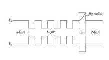
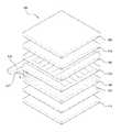
도 1은 일반적인 발광소자의 에너지 밴드 다이어그램을 나타낸 도면이다.1 is a diagram showing an energy band diagram of a general light emitting device.
도 1을 참조하면, 발광소자는 n-GaN층에서 주입된 전자와 p-GaN층에서 주입된 정공이 다중 우물 구조(MQW)로 이루어진 활성층에서 재결합함으로써 빛을 방출한다. 전자는 정공에 비하여 이동도가 뛰어나기 때문에 활성층에서 정공과 결합되지 못하고 p-GaN층으로 오버플로우되는 것을 방지하기 위하여 밴드갭이 큰 전자 차단층(EBL)을 삽입하는 것이 일반적이다. 이때, 활성층으로의 정공의 주입 효율을 향상시키기 위하여 전자 차단층에 Mg을 도핑하는데, 반도체층들의 결정성 품질 저하 등으로 인하여 Mg의 도핑 프로파일(Mg profile)의 피크가 활성층에서 먼 EBL의 한쪽 끝으로 치우쳐서 나타나며, 이로 인해 정공의 이동도 저하 및 발광 효율이 저하되는 문제점이 발생한다.Referring to FIG. 1, the light emitting device emits light by recombining electrons injected from the n-GaN layer and holes injected from the p-GaN layer into an active layer of a multi-well structure (MQW). Since electrons have better mobility than holes, it is common to insert an electron blocking layer (EBL) having a large bandgap in order to prevent the active layer from being coupled with holes and overflow to the p-GaN layer. At this time, Mg is doped in the electron blocking layer in order to improve the efficiency of injecting holes into the active layer. However, the peak of Mg doping profile (Mg profile) , Which results in a decrease in hole mobility and a decrease in luminous efficiency.
실시예는 활성층에 인접한 전자 차단층의 영역에서 도펀트의 주입 효율을 증대시켜 정공의 주입 효율과 발광 효율을 향상시키고자 한다.The embodiment attempts to improve the injection efficiency of the holes and the luminous efficiency by increasing the doping efficiency of the dopant in the region of the electron blocking layer adjacent to the active layer.
실시예에 따른 발광소자는 제1 도전형 반도체층; 제2 도전형 반도체층; 및 상기 제1 도전형 반도체층과 상기 제2 도전형 반도체층 사이에 위치하고, 상기 활성층에 인접하여 전자 차단층을 포함하는 제2 도전형 반도체층;을 포함하고, 상기 전자 차단층은 장벽층 및 상기 장벽층보다 에너지 밴드갭이 작은 우물층의 페어 구조를 복수 개 포함하며, 상기 전자 차단층은 상기 활성층에 인접하고 장벽층 및 우물층의 페어 구조를 적어도 하나 포함하는 제1 영역과, 상기 제1 영역 상에 위치하고 장벽층 및 우물층의 페어 구조를 적어도 하나 포함하는 제2 영역을 포함하고, 상기 제1 영역에 속하는 우물층의 두께가 상기 제2 영역에 속하는 우물층의 두께보다 두껍다.A light emitting device according to an embodiment includes a first conductive semiconductor layer; A second conductivity type semiconductor layer; And a second conductive type semiconductor layer disposed between the first conductive type semiconductor layer and the second conductive type semiconductor layer and including an electron blocking layer adjacent to the active layer, A first region including a pair of well layers having a smaller energy bandgap than the barrier layer, the first barrier layer being adjacent to the active layer and including at least one pair structure of a barrier layer and a well layer; And a second region located on the first region and including at least one pair structure of a barrier layer and a well layer, wherein a thickness of the well layer belonging to the first region is thicker than a thickness of the well layer belonging to the second region.
상기 제1 영역에 속하는 복수 개의 우물층은 상기 활성층에서 멀어지는 방향으로 갈수록 두께가 감소할 수 있다.The plurality of well layers belonging to the first region may decrease in thickness in a direction away from the active layer.
상기 제1 영역에 속하는 복수 개의 우물층 중에서 상기 활성층에 가장 인접한 우물층의 두께가 가장 두꺼울 수 있다.The thickness of the well layer closest to the active layer among the plurality of well layers belonging to the first region may be the thickest.
상기 전자 차단층에 속하는 복수 개의 우물층은 상기 활성층에서 멀어지는 방향으로 갈수록 두께가 감소할 수 있다.The thickness of the plurality of well layers belonging to the electron blocking layer may be decreased toward the direction away from the active layer.
상기 제1 영역에 속하는 장벽층의 두께가 상기 제2 영역에 속하는 장벽층의 두께보다 두꺼울 수 있다.The thickness of the barrier layer belonging to the first region may be thicker than the thickness of the barrier layer belonging to the second region.
상기 제1 영역에 속하는 복수 개의 장벽층은 상기 활성층에서 멀어지는 방향으로 갈수록 두께가 감소할 수 있다.The plurality of barrier layers belonging to the first region may decrease in thickness in a direction away from the active layer.
상기 제1 영역에 속하는 복수 개의 장벽층 중에서 상기 활성층에 가장 인접한 장벽층의 두께가 가장 두꺼울 수 있다.The thickness of the barrier layer closest to the active layer among the plurality of barrier layers belonging to the first region may be the largest.
상기 전자 차단층에 속하는 복수 개의 장벽층은 상기 활성층에서 멀어지는 방향으로 갈수록 두께가 감소할 수 있다.The thickness of the plurality of barrier layers belonging to the electron blocking layer may decrease in a direction away from the active layer.
상기 전자 차단층에 속하는 복수 개의 우물층 중에서 상기 활성층에 가장 인접한 적어도 하나의 우물층은 In을 포함하여 이루어질 수 있다.At least one well layer closest to the active layer among the plurality of well layers belonging to the electron blocking layer may include In.
상기 전자 차단층에 속하는 복수 개의 우물층 중에서 상기 활성층에 가장 인접한 적어도 하나의 우물층의 In 함량이 가장 높을 수 있다.The In content of the at least one well layer closest to the active layer among the plurality of well layers belonging to the electron blocking layer may be the highest.
상기 전자 차단층에 속하는 복수 개의 우물층 중에서 상기 활성층에 가장 인접한 적어도 하나의 우물층의 에너지 밴드갭이 가장 작을 수 있다.The energy band gap of at least one well layer closest to the active layer among the plurality of well layers belonging to the electron blocking layer may be the smallest.
상기 제2 도전형 반도체층은 상기 활성층과 상기 전자 차단층 사이에 정공 주입층을 더 포함할 수 있다.The second conductivity type semiconductor layer may further include a hole injection layer between the active layer and the electron blocking layer.
상기 전자 차단층에 속하는 복수 개의 장벽층 및 복수 개의 우물층 중에서 상기 활성층에 가장 인접한 장벽층의 두께가 가장 두꺼울 수 있다.The thickness of the barrier layer closest to the active layer among the plurality of barrier layers and the plurality of well layers belonging to the electron blocking layer may be the largest.
실시예에 따르면, 활성층에 인접한 전자 차단층의 영역에서의 도펀트의 주입 효율을 향상시킬 수 있다.According to the embodiment, the doping efficiency of the dopant in the region of the electron blocking layer adjacent to the active layer can be improved.
실시예에 따르면, 정공의 주입 효율이 개선됨으로써 발광소자의 발광 효율 및 파워가 향상될 수 있다.According to the embodiment, the injection efficiency of holes is improved, so that the luminous efficiency and power of the light emitting device can be improved.
도 1은 일반적인 발광소자의 에너지 밴드 다이어그램을 나타낸 도면.
도 2는 일실시예에 따른 발광소자의 측단면도.
도 3은 다른 실시예에 따른 발광소자의 측단면도.
도 4는 제1 실시예에 따른 발광소자에서 제2 도전형 반도체층 부분의 에너지 밴드 다이어그램을 나타낸 도면.
도 5는 제2 실시예에 따른 발광소자에서 제2 도전형 반도체층 부분의 에너지 밴드 다이어그램을 나타낸 도면.
도 6은 제3 실시예에 따른 발광소자에서 제2 도전형 반도체층 부분의 에너지 밴드 다이어그램을 나타낸 도면.
도 7은 제4 실시예에 따른 발광소자에서 제2 도전형 반도체층 부분의 에너지 밴드 다이어그램을 나타낸 도면.
도 8은 제5 실시예에 따른 발광소자에서 제2 도전형 반도체층 부분의 에너지 밴드 다이어그램을 나타낸 도면.
도 9는 제6 실시예에 따른 발광소자에서 제2 도전형 반도체층 부분의 에너지 밴드 다이어그램을 나타낸 도면.
도 10 내지 도 12는 발광소자의 제작 과정의 일실시예를 간략히 도시한 도면.
도 13은 전류 밀도에 따른 발광 효율을 종래의 경우와 비교하여 나타낸 그래프.
도 14는 파장에 따른 발광소자의 파워를 종래의 경우와 비교하여 나타낸 그래프.
도 15는 실시예들에 따른 발광소자를 포함한 발광소자 패키지의 일실시예를 도시한 도면.
도 16은 실시예들에 따른 발광소자 또는 발광소자 패키지가 배치된 헤드램프의 일실시예를 도시한 도면.
도 17은 실시예에 따른 발광소자 패키지가 배치된 표시장치의 일실시예를 도시한 도면.BRIEF DESCRIPTION OF THE DRAWINGS FIG. 1 is an energy band diagram of a general light emitting device. FIG.
2 is a side cross-sectional view of a light emitting device according to one embodiment.
3 is a side cross-sectional view of a light emitting device according to another embodiment.
4 is an energy band diagram of a portion of the second conductivity type semiconductor layer in the light emitting device according to the first embodiment.
5 is an energy band diagram of a portion of the second conductivity type semiconductor layer in the light emitting device according to the second embodiment.
6 is an energy band diagram of a portion of the second conductivity type semiconductor layer in the light emitting device according to the third embodiment.
7 is an energy band diagram of a portion of the second conductivity type semiconductor layer in the light emitting device according to the fourth embodiment.
8 is an energy band diagram of a portion of the second conductivity type semiconductor layer in the light emitting device according to the fifth embodiment.
9 is an energy band diagram of a portion of the second conductivity type semiconductor layer in the light emitting device according to the sixth embodiment.
10 to 12 are views schematically showing an embodiment of a manufacturing process of a light emitting device.
13 is a graph showing a comparison of the luminous efficiency according to the current density with the conventional case.
14 is a graph showing the power of the light emitting device according to the wavelength in comparison with the conventional case.
15 is a view illustrating an embodiment of a light emitting device package including the light emitting device according to the embodiments.
16 is a view illustrating an embodiment of a headlamp in which a light emitting device or a light emitting device package according to embodiments is disposed.
17 is a view illustrating a display device in which a light emitting device package according to an embodiment is disposed.
이하 상기의 목적을 구체적으로 실현할 수 있는 본 발명의 바람직한 실시예를 첨부한 도면을 참조하여 설명한다.DETAILED DESCRIPTION OF THE PREFERRED EMBODIMENTS Hereinafter, preferred embodiments of the present invention will be described with reference to the accompanying drawings.
본 발명에 따른 실시예의 설명에 있어서, 각 element의 " 상(위) 또는 하(아래)(on or under)"에 형성되는 것으로 기재되는 경우에 있어, 상(위) 또는 하(아래)(on or under)는 두개의 element가 서로 직접(directly)접촉되거나 하나 이상의 다른 element가 상기 두 element사이에 배치되어(indirectly) 형성되는 것을 모두 포함한다. 또한 “상(위) 또는 하(아래)(on or under)”으로 표현되는 경우 하나의 element를 기준으로 위쪽 방향뿐만 아니라 아래쪽 방향의 의미도 포함할 수 있다.In the description of the embodiment according to the present invention, in the case of being described as being formed "on or under" of each element, the upper (upper) or lower (lower) or under are all such that two elements are in direct contact with each other or one or more other elements are indirectly formed between the two elements. Also, when expressed as "on or under", it may include not only an upward direction but also a downward direction with respect to one element.
도면에서 각층의 두께나 크기는 설명의 편의 및 명확성을 위하여 과장되거나 생략되거나 또는 개략적으로 도시되었다. 또한 각 구성요소의 크기는 실제크기를 전적으로 반영하는 것은 아니다.The thickness and size of each layer in the drawings are exaggerated, omitted, or schematically shown for convenience and clarity of explanation. Also, the size of each component does not entirely reflect the actual size.
도 2는 일실시예에 따른 발광소자의 측단면도이다.2 is a side cross-sectional view of a light emitting device according to an embodiment.
도 2를 참조하면, 일실시예에 따른 발광소자(100)는 제1 도전형 반도체층(122), 제2 도전형 반도체층(126), 및 상기 제1 도전형 반도체층(122)과 제2 도전형 반도체층(126) 사이의 활성층(124)을 포함한다.2, the
제1 도전형 반도체층(122)과 활성층(124) 및 제2 도전형 반도체층(126)을 합하여 발광 구조물(120)이라 칭할 수 있다.The first
발광소자(100)는 복수의 화합물 반도체층, 예를 들어 3족-5족 또는 2족-6족 원소의 반도체층을 이용한 LED(Light Emitting Diode)를 포함하며, LED는 청색, 녹색 또는 적색 등과 같은 광을 방출하는 유색 LED이거나, 백색 LED 또는 UV LED일 수 있다. LED의 방출 광은 다양한 반도체를 이용하여 구현될 수 있으며, 이에 대해 한정하지는 않는다.The
발광 구조물(120)은 예를 들어, 유기금속 화학 증착법(MOCVD; Metal Organic Chemical Vapor Deposition), 화학 증착법(CVD; Chemical Vapor Deposition), 플라즈마 화학 증착법(PECVD; Plasma-Enhanced Chemical Vapor Deposition), 분자선 성장법(MBE; Molecular Beam Epitaxy), 수소화물 기상 성장법(HVPE; Hydride Vapor Phase Epitaxy) 등의 방법을 이용하여 형성될 수 있으며, 이에 대해 한정하지는 않는다.The
제1 도전형 반도체층(122)은 반도체 화합물로 형성될 수 있으며, 예를 들어 3족-5족 또는 2족-6족 등의 화합물 반도체로 형성될 수 있다. 또한 제1 도전형 도펀트가 도핑될 수 있다. 상기 제1 도전형 반도체층(122)이 n형 반도체층인 경우, 상기 제1 도전형 도펀트는 n형 도펀트로서 Si, Ge, Sn, Se, Te 등을 포함할 수 있으나 이에 한정되지 않는다. 상기 제1 도전형 반도체층(122)이 p형 반도체층인 경우, 상기 제1 도전형 도펀트는 p형 도펀트로서 Mg, Zn, Ca, Sr, Ba 등을 포함할 수 있으나 이에 한정하지 않는다.The first
제1 도전형 반도체층(122)은 AlxInyGa(1-x-y)N (0≤x≤1, 0≤y≤1, 0≤x+y≤1)의 조성식을 갖는 반도체 물질을 포함할 수 있다. 상기 제1 도전형 반도체층(122)은 GaN, InN, AlN, InGaN, AlGaN, InAlGaN, AlInN, AlGaAs, InGaAs, AlInGaAs, GaP, AlGaP, InGaP, AlInGaP, InP 중 어느 하나 이상으로 형성될 수 있다.The first
제2 도전형 반도체층(126)은 반도체 화합물로 형성될 수 있으며, 예를 들어 3족-5족 또는 2족-6족 등의 화합물 반도체로 형성될 수 있다. 또한 제2 도전형 도펀트가 도핑될 수 있다. 제2 도전형 반도체층(126)은 예를 들어, InxAlyGa1-x-yN (0≤x≤1, 0≤y≤1, 0≤x+y≤1)의 조성식을 갖는 반도체 물질을 포함할 수 있다. 상기 제2 도전형 반도체층(126)이 p형 반도체층인 경우, 상기 제2 도전형 도펀트는 p형 도펀트로서, Mg, Zn, Ca, Sr, Ba 등을 포함할 수 있으나 이에 한정하지 않는다. 상기 제2 도전형 반도체층(126)이 n형 반도체층인 경우, 상기 제2 도전형 도펀트는 n형 도펀트로서 Si, Ge, Sn, Se, Te 등을 포함할 수 있으나 이에 한정되지 않는다.The second
이하에서는, 제1 도전형 반도체층(122)이 n형 반도체층, 제2 도전형 반도체층(126)이 p형 반도체층인 경우를 예로 들어 설명한다.Hereinafter, the case where the first conductivity
상기 제2 도전형 반도체층(126) 상에는 상기 제2 도전형과 반대의 극성을 갖는 반도체, 예컨대 상기 제2 도전형 반도체층(126)이 p형 반도체층일 경우 n형 반도체층(미도시)을 형성할 수 있다. 이에 따라 발광 구조물은 n-p 접합 구조, p-n 접합 구조, n-p-n 접합 구조, p-n-p 접합 구조 중 어느 한 구조로 구현할 수 있다.An n-type semiconductor layer (not shown) may be formed on the second conductive
제1 도전형 반도체층(122)과 제2 도전형 반도체층(126) 사이에 활성층(124)이 위치한다.The
활성층(124)은 전자와 정공이 서로 만나서 활성층(발광층) 물질 고유의 에너지 밴드에 의해서 결정되는 에너지를 갖는 빛을 방출하는 층이다. 제1 도전형 반도체층(122)이 n형 반도체층이고 제2 도전형 반도체층(126)이 p형 반도체층인 경우, 상기 제1 도전형 반도체층(122)으로부터 전자가 주입되고 상기 제2 도전형 반도체층(126)으로부터 정공이 주입될 수 있다.The
활성층(124)은 단일 우물 구조, 다중 우물 구조, 양자선(Quantum-Wire) 구조, 또는 양자 점(Quantum Dot) 구조 중 적어도 어느 하나로 형성될 수 있다. 예를 들어, 상기 활성층(124)은 트리메틸 갈륨 가스(TMGa), 암모니아 가스(NH3), 질소 가스(N2), 및 트리메틸 인듐 가스(TMIn)가 주입되어 다중 양자 우물 구조가 형성될 수 있으나 이에 한정되는 것은 아니다.The
활성층(124)이 다중 우물 구조로 이루어진 경우, 서로 번갈아 위치하는 복수 개의 우물층과 장벽층을 포함하며, 활성층(124)의 우물층/장벽층은 InGaN/GaN, InGaN/InGaN, GaN/AlGaN, InAlGaN/GaN, GaAs(InGaAs)/AlGaAs, GaP(InGaP)/AlGaP 중 어느 하나 이상의 페어 구조로 형성될 수 있으나 이에 한정되지 않는다. 우물층은 장벽층의 밴드갭보다 작은 밴드갭을 갖는 물질로 형성될 수 있다.InGaN / InGaN, InGaN / InGaN, InGaN / InGaN, InGaN / InGaN, InGaN / InGaN, InGaN / InGaN, and InGaN / InGaN, But may be formed of any one or more pairs of InAlGaN / GaN, GaAs (InGaAs) / AlGaAs, GaP (InGaP) / AlGaP, but is not limited thereto. The well layer may be formed of a material having a band gap smaller than the band gap of the barrier layer.
제2 도전형 반도체층(126)은 활성층(124)에 인접하여 위치하는 전자 차단층(Electron Blocking Layer: EBL, 200)을 포함한다.The second
전자 차단층(200)은 제1 도전형 반도체층(122)에서 제공되는 전자의 이동도(mobility)가 높기 때문에, 전자가 발광에 기여하지 못하고 활성층(124)을 넘어 제2 도전형 반도체층(126)으로 빠져나가 누설 전류의 원인이 되는 것을 방지하는 전위 장벽의 역할을 한다.The
전자 차단층(200)은 장벽층 및 상기 장벽층보다 에너지 밴드갭이 작은 우물층의 페어 구조를 복수 개 포함한다. 전자 차단층(200)은 활성층(124)보다 큰 에너지 밴드갭을 갖는 물질로 형성되며, InxAlyGa1-x-yN(0≤x<y<1)의 조성을 가질 수 있다.The
전자 차단층(200)에 대해서는 도 4 내지 도 9를 참조하여 자세히 후술하기로 한다.The
발광 구조물(120)은 기판(110) 상에 위치한다.The
기판(110)은 반도체 물질 성장에 적합한 재료, 열전도성이 뛰어난 물질로 형성될 수 있다. 기판(110)은 예를 들어, 사파이어(Al2O3), SiC, GaAs, GaN, ZnO, Si, GaP, InP, Ge, and Ga203 중 적어도 하나를 사용할 수 있다. 기판(110)에 대해 습식세척을 하여 표면의 불순물을 제거할 수 있다.The
발광 구조물(120)과 기판(110) 사이에는 버퍼층(115)이 위치할 수 있다. 버퍼층(115)은 발광 구조물(120)과 기판(110)의 재료의 격자 부정합 및 열팽창 계수의 차이를 완화하기 위한 것이다. 버퍼층(115)의 재료는 3족-5족 화합물 반도체, 예컨대, GaN, InN, AlN, InGaN, InAlGaN, AlInN 중 적어도 하나로 형성될 수 있다.A
기판(110)과 제1 도전형 반도체층(122) 사이에 언도프트 반도체층(미도시)이 위치할 수도 있다. 언도프트 반도체층은 제1 도전형 반도체층(122)의 결정성 향상을 위해 형성되는 층으로, n형 도펀트가 도핑되지 않아 제1 도전형 반도체층에 비해 낮은 전기전도성을 갖는 것을 제외하고는 상기 제1 도전형 반도체층(122)과 같을 수 있다.An undoped semiconductor layer (not shown) may be disposed between the
제1 도전형 반도체층(122)은 제2 도전형 반도체층(126)과 활성층(124)의 적어도 일부가 선택적으로 식각되어 노출된 노출면(S)을 갖는다. 상기 노출면(S) 상에 제1 전극(130)이 위치하고, 식각되지 않은 제2 도전형 반도체층(126) 상에 제2 전극(140)이 위치한다.The first
제1 전극(130) 및 제2 전극(140)은 몰리브덴(Mo), 크롬(Cr), 니켈(Ni), 금(Au), 알루미늄(Al), 타이타늄(Ti), 백금(Pt), 바나듐(V), 텅스텐(W), 납(Pd), 구리(Cu), 로듐(Rh) 또는 이리듐(Ir) 중 적어도 하나를 포함하여 단층 또는 다층 구조로 형성될 수 있다.The
제2 전극(140)이 형성되기 전 제2 도전형 반도체층(126) 상에는 도전층(150)이 형성될 수 있다.The
실시예에 따라, 제2 도전형 반도체층(126)이 노출되도록 도전층(150)의 일부가 오픈되어 제2 도전형 반도체층(126)과 제2 전극(140)이 접할 수 있다.A part of the
또는, 도 2에 도시된 바와 같이, 도전층(150)을 사이에 두고 제2 도전형 반도체층(126)과 제2 전극(140)이 전기적으로 연결될 수도 있다.Alternatively, as shown in FIG. 2, the second
도전층(150)은 제2 도전형 반도체층(126)의 전기적 특성을 향상시키고 제2 전극(140)과의 전기적 접촉을 개선하기 위한 것으로, 층 또는 복수의 패턴으로 형성될 수 있다. 도전층(150)은 투과성을 갖는 투명 전극층으로 형성될 수 있다.The
도전층(150)에는 투광성 전도층과 금속이 선택적으로 사용될 수 있으며, 예를 들어, ITO(indium tin oxide), IZO(indium zinc oxide), IZTO(indium zinc tin oxide), IAZO(indium aluminum zinc oxide), IGZO(indium gallium zinc oxide), IGTO(indium gallium tin oxide), AZO(aluminum zinc oxide), ATO(antimony tin oxide), GZO(gallium zinc oxide), IZON(IZO Nitride), AGZO(Al-Ga ZnO), IGZO(In-Ga ZnO), ZnO, IrOx, RuOx, NiO, RuOx/ITO, Ni/IrOx/Au, 또는 Ni/IrOx/Au/ITO, Ag, Ni, Cr, Ti, Al, Rh, Pd, Ir, Sn, In, Ru, Mg, Zn, Pt, Au, Hf 중 적어도 하나를 포함하여 형성될 수 있으나, 이러한 재료에 한정되지 않는다.For example, the
도 2에 따른 발광소자(100)는 수평형(Lateral) 구조일 수 있다. 수평형 구조란, 발광 구조물(120)에서 제1 전극(130)과 제2 전극(140)이 동일한 방향을 향해 형성되는 구조를 의미한다. 일 예로서, 도 2를 참조하면, 제1 전극(130)과 제2 전극(140)이 발광 구조물(120)의 상부 방향으로 형성되어 있다.The
도 3은 다른 실시예에 따른 발광소자의 측단면도다. 상술한 내용과 중복되는 내용은 다시 설명하지 않는다.3 is a side sectional view of a light emitting device according to another embodiment. The contents overlapping with those described above will not be described again.
도 3을 참조하면, 다른 실시예에 따른 발광소자(100)는 제1 도전형 반도체층(122), 제2 도전형 반도체층(126), 및 상기 제1 도전형 반도체층(122)과 제2 도전형 반도체층(126) 사이의 활성층(124)을 포함한다.Referring to FIG. 3, the
제1 도전형 반도체층(122)과 활성층(124) 및 제2 도전형 반도체층(126)을 합하여 발광 구조물(120)이라 칭할 수 있다.The first
제2 도전형 반도체층(126)은 활성층(124)에 인접하여 위치하는 전자 차단층(Electron Blocking Layer: EBL, 200)을 포함한다.The second
전자 차단층(200)은 제1 도전형 반도체층(122)에서 제공되는 전자의 이동도(mobility)가 높기 때문에, 전자가 발광에 기여하지 못하고 활성층(124)을 넘어 제2 도전형 반도체층(126)으로 빠져나가 누설 전류의 원인이 되는 것을 방지하는 전위 장벽의 역할을 한다.The
전자 차단층(200)은 장벽층 및 상기 장벽층보다 에너지 밴드갭이 작은 우물층의 페어 구조를 복수 개 포함한다. 전자 차단층(200)은 활성층(124)보다 큰 에너지 밴드갭을 갖는 물질로 형성되며, InxAlyGa1-x-yN(0≤x<y<1)의 조성을 가질 수 있다.The
전자 차단층(200)에 대해서는 도 4 내지 도 9를 참조하여 자세히 후술하기로 한다.The
발광 구조물(120)의 상부, 즉 제1 도전형 반도체층(122)의 일면에 제1 전극(130)이 위치하고, 발광 구조물(120)의 하부, 즉 제2 도전형 반도체층(126)의 일면에 제2 전극층(160)이 위치한다.The
일 예로서, 제2 전극층(160)은 도전층(160a) 또는 반사층(160b) 중 적어도 어느 하나를 포함할 수 있다.As an example, the
도전층(160a)은 제2 도전형 반도체층(126)의 전기적 특성을 개선하기 위한 것으로, 제2 도전형 반도체층(126)과 접하여 위치할 수 있다.The
도전층(160a)은 투명 전극층 또는 불투명 전극층으로 형성될 수 있으며, 예를 들어, ITO(indium tin oxide), IZO(indium zinc oxide), IZTO(indium zinc tin oxide), IAZO(indium aluminum zinc oxide), IGZO(indium gallium zinc oxide), IGTO(indium gallium tin oxide), AZO(aluminum zinc oxide), ATO(antimony tin oxide), GZO(gallium zinc oxide), IZON(IZO Nitride), AGZO(Al-Ga ZnO), IGZO(In-Ga ZnO), ZnO, IrOx, RuOx, NiO, RuOx/ITO, Ni/IrOx/Au, 또는 Ni/IrOx/Au/ITO, Ag, Ni, Cr, Ti, Al, Rh, Pd, Ir, Sn, In, Ru, Mg, Zn, Pt, Au, Hf 중 적어도 하나를 포함하여 형성될 수 있으며, 이러한 재료에 한정되지는 않는다.The
반사층(160b)은 활성층(124)에서 생성된 빛을 반사시켜 발광소자(100)의 내부에서 소멸되는 빛의 양을 줄임으로써, 발광소자(100)의 외부양자효율을 향상시킬 수 있다.The
반사층(160b)은 Ag, Ti, Ni, Cr 또는 AgCu 중 적어도 어느 하나를 포함할 수 있으나, 이에 한정하지 않는다.The
반사층(160b)이 제2 도전형 반도체층(126)과 오믹 접촉하는 물질로 이루어진 경우, 도전층(160a)은 별도로 형성하지 않을 수 있다.When the
발광 구조물(120)은 지지기판(180)에 의해 지지된다.The
지지기판(180)은 전기 전도성과 열 전도성이 높은 물질로 형성되며, 예를 들어, 소정의 두께를 갖는 베이스 기판(substrate)으로서, 몰리브덴(Mo), 실리콘(Si), 텅스텐(W), 구리(Cu) 또는 알루미늄(Al)로 구성되는 군으로부터 선택되는 물질 또는 이들의 합금으로 이루어질 수 있으며, 또한, 금(Au), 구리합금(Cu Alloy), 니켈(Ni), 구리-텅스텐(Cu-W), 캐리어 웨이퍼(예: GaN, Si, Ge, GaAs, ZnO, SiGe, SiC, SiGe, Ga2O3 등) 또는 전도성 시트 등을 선택적으로 포함할 수 있다.The
발광 구조물(120)은 본딩층(185)에 의해 지지기판(120)에 본딩될 수 있다. 이때, 발광 구조물(120) 하부에 위치하는 제2 전극층(160)과 본딩층(185)이 접할 수 있다.The
본딩층(185)은 베리어 금속 또는 본딩 금속 등을 포함하며, 예를 들어, Ti, Au, Sn, Ni, Cr, Ga, In, Bi, Cu, Ag 또는 Ta 중 적어도 하나를 포함할 수 있으며, 이에 대해 한정하지는 않는다.The
본딩층(185)은 발광 구조물(120)에 인접하여 확산 방지층(미도시)을 포함하여, 본딩층(185)에 사용된 금속 등이 상부의 발광 구조물(120) 내부로 확산되는 것을 방지할 수도 있다.The
발광 구조물(120)의 하부 둘레에 채널층(170)이 위치할 수 있다. 채널층(170)은 발광 구조물(120)을 보호하며, 발광소자(100)의 제조 과정 중 아이솔레이션 에칭시 에칭의 스톱 레이어(stop layer)로서 기능할 수 있다.The
채널층(170)은 발광 구조물(120)의 제2 도전형 반도체층(126) 하부 둘레에 루프 형상, 고리 형상 또는 프레임 형상 등의 패턴으로 형성될 수 있다.The
채널층(170)은 발광 구조물의 외벽이 습기에 노출되더라도 서로 쇼트가 발생하는 것을 방지하여 고습에 강한 발광소자를 제공할 수 있다.The
채널층(170)은 산화물, 질화물 또는 절연층의 재질 중에서 선택될 수 있으며, 예컨대 ITO(indium tinoxide), IZO(indium zinc oxide), IZTO(indium zinc tin oxide), IAZO(indium aluminum zinc oxide), IGZO(indium gallium zinc oxide), IGTO(indium gallium tin oxide), AZO(aluminum zinc oxide), ATO(antimony tin oxide), GZO(gallium zinc oxide), SiO2, SiOx, SiOxNy, Si3N4, Al2O3, TiO2 등에서 선택적으로 형성될 수 있으나, 이에 한정하지 않는다.The
발광 구조물(120) 상의 적어도 일부, 측면, 그리고 발광 구조물(120)의 외부로 노출된 채널층(170)의 상부에 패시베이션층(190)이 위치할 수도 있다.The
패시베이션층(190)은 산화물 또는 질화물로 이루어져 발광 구조물(120)을 보호할 수 있다. 일 예로서, 패시베이션층(190)은 실리콘 산화물(SiO2)층, 실리콘 질화물층, 산화 질화물층, 또는 산화 알루미늄층으로 이루어질 수 있으나, 이에 한정하지 않는다.The
발광 구조물(120)의 제1 도전형 반도체층(122) 상에는 러프니스 패턴(R)이 형성될 수 있다. 발광 구조물(120)의 상부에 패시베이션층(190)이 존재하는 경우, 상기 패시베이션층(190)에 러프니스 패턴(R)이 위치할 수도 있다. 러프니스 패턴(R)은 PEC(Photo enhanced chemical) 식각 방법이나 마스크 패턴을 이용한 에칭 공정 수행하여 형성할 수 있다. 러프니스 패턴(R)은 활성층(124)에서 생성된 광의 외부 추출 효율을 증가시키기 위한 것으로서, 규칙적인 주기를 갖거나 불규칙적인 주기를 가질 수 있다.The roughness pattern R may be formed on the first conductivity
도 3에 따른 발광소자(100)는 수직형(Vertical) 구조일 수 있다. 수직형 구조란, 발광소자(100)에서 제1 전극(130)과 제2 전극층(160)이 서로 다른 방향에 각각 형성되는 구조를 의미한다. 일 예로서, 도 3을 참조하면, 발광 구조물(120)의 상부 방향으로 제1 전극(130)이 형성되고 발광 구조물(120)의 하부 방향으로 제2 전극층(160)이 형성되어 있다.The
이하에서는 도 4 내지 도 9를 참조하여, 제2 도전형 반도체층(126)의 전자 주입층(200)에 대하여 좀 더 자세히 설명한다. 도 4 내지 도 9에 따른 발광소자는 상술한 수평형 구조 또는 수직형 구조로 형성될 수 있다.Hereinafter, the
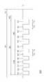
도 4는 제1 실시예에 따른 발광소자에서 제2 도전형 반도체층 부분의 에너지 밴드 다이어그램을 나타낸 도면이다.4 is an energy band diagram of a portion of the second conductivity type semiconductor layer in the light emitting device according to the first embodiment.
도 4를 참조하면, 제1 실시예에 따른 발광소자(100A)는 제1 도전형 반도체층(122)과 활성층(124) 및 제2 도전형 반도체층(126)을 포함하고, 상기 제2 도전형 반도체층(126)은 활성층(124)과 인접하여 위치하는 전자 차단층(200)을 포함한다.Referring to FIG. 4, the
전자 차단층(200)은 활성층(124)보다 큰 에너지 밴드갭을 갖는 물질로 형성되며, InxAlyGa1-x-yN(0≤x<y<1)의 조성을 가질 수 있다.The
전자 차단층(200)은 장벽층(210) 및 상기 장벽층(210)보다 에너지 밴드갭이 작은 우물층(220)의 페어 구조를 복수 개 포함한다. 도 4에는 일 예로서, 여섯 개의 장벽층(210)/우물층(220)의 페어 구조를 포함하는 것으로 도시하였으나, 이에 한정하지 않는다.The
전자 차단층(200)은 활성층(124)에 인접하고 장벽층(210) 및 우물층(220)의 페어 구조를 적어도 하나 포함하는 제1 영역(200-1)과, 상기 제1 영역(200-1) 상에 위치하고 장벽층(210) 및 우물층(220)의 페어 구조를 적어도 하나 포함하는 제2 영역(200-2)을 포함한다.The
제1 영역(200-1)에 속하는 우물층(220)의 두께(d1-2)는 제2 영역(200-2)에 속하는 우물층(220)의 두께(d2-2)보다 두껍다(d1-2>d2-2).The thickness d1-2 of the
우물층(220)의 두께(d1-2)란 제1 영역(200-1)에 속하는 복수 개의 우물층들(220) 각각의 두께를 의미하며, 우물층(220)의 두께(d2-2)란 제2 영역(200-2)에 속하는 우물층들(220) 각각의 두께를 의미한다.The thickness d1-2 of the
우물층(200)이 두꺼울수록 제2 도전형 도펀트의 주입률이 증가하므로, 활성층(124)에 인접한 전자 차단층(200)의 제1 영역(200-1)에 속하는 우물층(220)을 제2 영역(200-2)에 속하는 우물층(220)보다 두껍게 형성함으로써, 전자 차단층(200)의 앞단에서의 도펀트의 주입 효율을 개선할 수 있다.The injection rate of the second conductivity type dopant increases as the
즉, 종래의 발광소자의 경우, 결정성 품질 저하 및 응력으로 인하여 활성층에서 먼 전자 차단층의 한 쪽 끝으로 도펀트의 주입률이 치우치는 경향이 있었으나, 실시예에 따르면 활성층(124)에 인접한 전자 차단층(200)의 앞단에서의 도펀트의 주입 효율을 개선하여 정공의 주입 효율 및 발광소자의 발광 효율을 향상시킬 수 있다.That is, in the case of the conventional light emitting device, the injection rate of the dopant tends to be shifted toward one end of the electron blocking layer far from the active layer due to the deterioration in crystallinity and the stress. However, according to the embodiment, The injection efficiency of the dopant at the front end of the
전차 차단층(200)의 제2 도전형 도펀트의 도핑 농도는 5*1019~1.5*1020일 수 있으나, 이에 한정하지 않는다.The doping concentration of the second conductive dopant in the
제1 영역(200-1) 내에서 복수 개의 우물층(220) 각각의 두께(d1-2)는 일정할 수 있다. 또한, 제2 영역(200-2) 내에서 복수 개의 우물층(200) 각각의 두께(d2-2) 역시 일정할 수 있다.The thickness d1-2 of each of the plurality of
전자 차단층(200) 전체 두께는 400Å 내지 500Å일 수 있으나, 이에 한정하지 않는다. 실시예에 따라, 전자 차단층(200)에서 제1 영역(200-1)의 두께와 제2 영역(200-2)가 동일할 수도 있고, 제1 영역(200-1)의 두께와 제2 영역(200-2)가 서로 다를 수도 있다.The total thickness of the
전자 차단층(200)의 장벽층(210)의 두께(d1)는 일정할 수 있다. 장벽층(210)의 두께(d1)란 전자 차단층(200)에 속하는 복수 개의 장벽층들(210) 각각의 두께를 의미할 수 있다.The thickness d1 of the
제2 도전형 반도체층(126)은 활성층(124)과 전자 차단층(200) 사이에 정공 주입층(126a)을 더 포함할 수 있다. 정공 주입층(126a)은 활성층(124)으로 정공을 제공하는 역할을 한다. 전자 차단층(200)의 큰 에너지 밴드갭으로 인하여 활성층(124)으로의 정공 주입률이 저하될 수 있는데, 활성층(124)과 전자 차단층(200) 사이에 정공 주입층(126a)을 삽입함으로써, 정공의 주입 효율이 향상될 수 있다. 정공 주입층(126a)의 에너지 밴드갭은 전자 차단층(200)의 에너지 밴드갭보다 작으며, 활성층(124)의 장벽층의 에너지 밴드갭과 동일할 수 있다.The second
도 5는 제2 실시예에 따른 발광소자에서 제2 도전형 반도체층 부분의 에너지 밴드 다이어그램을 나타낸 도면이다. 상술한 실시예들과 중복되는 내용은 다시 설명하지 않으며, 이하에서는 차이점을 중심으로 설명한다.5 is an energy band diagram of a portion of the second conductivity type semiconductor layer in the light emitting device according to the second embodiment. The contents overlapping with the above-described embodiments will not be described again, and the differences will be mainly described below.
도 5를 참조하면, 제2 실시예에 따른 발광소자(100B)는 제1 도전형 반도체층(122)과 활성층(124) 및 제2 도전형 반도체층(126)을 포함하고, 상기 제2 도전형 반도체층(126)은 활성층(124)과 인접하여 위치하는 전자 차단층(200)을 포함한다.5, the
전자 차단층(200)은 활성층(124)보다 큰 에너지 밴드갭을 갖는 물질로 형성되며, InxAlyGa1-x-yN(0≤x<y<1)의 조성을 가질 수 있다.The
전자 차단층(200)은 장벽층(210) 및 상기 장벽층(210)보다 에너지 밴드갭이 작은 우물층(220)의 페어 구조를 복수 개 포함한다. 도 5에는 일 예로서, 여섯 개의 장벽층(210)/우물층(220)의 페어 구조를 포함하는 것으로 도시하였으나, 이에 한정하지 않는다.The
전자 차단층(200)은 활성층(124)에 인접하고 장벽층(210) 및 우물층(220)의 페어 구조를 적어도 하나 포함하는 제1 영역(200-1)과, 상기 제1 영역(200-1) 상에 위치하고 장벽층(210) 및 우물층(220)의 페어 구조를 적어도 하나 포함하는 제2 영역(200-2)을 포함한다.The
제1 영역(200-1)에 속하는 우물층(220)의 두께(d1-2)는 제2 영역(200-2)에 속하는 우물층(220)의 두께(d2-2)보다 두껍다(d1-2>d2-2). 그리고, 제1 영역(200-1)에 속하는 복수 개의 우물층(220) 각각의 두께(d1-2)는 활성층(124)에서 멀어지는 방향으로 갈수록 두께가 감소할 수 있다.The thickness d1-2 of the
제1 영역(200-1)에 속하는 복수 개의 우물층(220) 중에서 활성층(124)에 가장 인접한 우물층(220)의 두께가 가장 두껍다.The thickness of the
실시예에 따르면, 활성층(124)에 인접한 전자 차단층(200)의 제1 영역(200-1)에 속하는 우물층(220)을 제2 영역(200-2)에 속하는 우물층(220)보다 두껍게 형성하되, 제1 영역(200-1) 내에서 활성층(124)에 가까워지는 방향으로 갈수록 우물층(220)을 두껍게 형성함으로써, 전자 차단층(200)의 앞단에서의 도펀트의 주입 효율을 개선하여 정공의 주입 효율 및 발광소자의 발광 효율을 향상시킬 수 있다.The
도 5에는 제1 영역(200-1)에 속하는 복수 개의 우물층(220) 모두에서 두께(d1-2)의 변화가 있는 것으로 도시하였으나, 실시예에 따라, 인접한 적어도 두 개의 우물층(220)의 두께(d1-2)는 일정할 수도 있다.5 shows that the thickness d1-2 varies in all of the plurality of
제2 영역(200-2) 내에서 복수 개의 우물층(200) 각각의 두께(d2-2)는 일정할 수 있다. 또한, 전자 차단층(200)의 장벽층(210)의 두께(d1)는 일정할 수 있다.The thickness d2-2 of each of the plurality of
제2 도전형 반도체층(126)은 활성층(124)과 전자 차단층(200) 사이에 정공 주입층(126a)을 더 포함할 수 있다. 정공 주입층(126a)은 활성층(124)으로 정공을 제공하는 역할을 한다. 전자 차단층(200)의 큰 에너지 밴드갭으로 인하여 활성층(124)으로의 정공 주입률이 저하될 수 있는데, 활성층(124)과 전자 차단층(200) 사이에 정공 주입층(126a)을 삽입함으로써, 정공의 주입 효율이 향상될 수 있다. 정공 주입층(126a)의 에너지 밴드갭은 전자 차단층(200)의 에너지 밴드갭보다 작으며, 활성층(124)의 장벽층의 에너지 밴드갭과 동일할 수 있다.The second
도 6은 제3 실시예에 따른 발광소자에서 제2 도전형 반도체층 부분의 에너지 밴드 다이어그램을 나타낸 도면이다. 상술한 실시예들과 중복되는 내용은 다시 설명하지 않으며, 이하에서는 차이점을 중심으로 설명한다.6 is an energy band diagram of a portion of the second conductivity type semiconductor layer in the light emitting device according to the third embodiment. The contents overlapping with the above-described embodiments will not be described again, and the differences will be mainly described below.
도 6을 참조하면, 제3 실시예에 따른 발광소자(100B)는 제1 도전형 반도체층(122)과 활성층(124) 및 제2 도전형 반도체층(126)을 포함하고, 상기 제2 도전형 반도체층(126)은 활성층(124)과 인접하여 위치하는 전자 차단층(200)을 포함한다.6, the
전자 차단층(200)은 활성층(124)보다 큰 에너지 밴드갭을 갖는 물질로 형성되며, InxAlyGa1-x-yN(0≤x<y<1)의 조성을 가질 수 있다.The
전자 차단층(200)은 장벽층(210) 및 상기 장벽층(210)보다 에너지 밴드갭이 작은 우물층(220)의 페어 구조를 복수 개 포함한다. 도 6에는 일 예로서, 여섯 개의 장벽층(210)/우물층(220)의 페어 구조를 포함하는 것으로 도시하였으나, 이에 한정하지 않는다.The
전자 차단층(200)은 활성층(124)에 인접하고 장벽층(210) 및 우물층(220)의 페어 구조를 적어도 하나 포함하는 제1 영역(200-1)과, 상기 제1 영역(200-1) 상에 위치하고 장벽층(210) 및 우물층(220)의 페어 구조를 적어도 하나 포함하는 제2 영역(200-2)을 포함한다.The
제1 영역(200-1)에 속하는 우물층(220)의 두께(d1-2)는 제2 영역(200-2)에 속하는 우물층(220)의 두께(d2-2)보다 두껍다(d1-2>d2-2). 그리고, 전자 차단층(200)에 속하는 복수 개의 우물층(220)은 활성층(124)에서 멀어지는 방향으로 갈수록 두께가 감소할 수 있다.The thickness d1-2 of the
종래의 발광소자의 경우, 전자 차단층 내에서의 도펀트 주입 프로파일이 조금씩 증가하다가 활성층에서 먼 한 쪽 끝에서 피크 지점이 나타나면서 활성층으로의 정공의 주입률이 떨어지는 문제점이 있었으나, 실시예에 따르면, 활성층(124)에 인접한 전자 차단층(200)의 부분에서부터 활성층(124)에서 멀어지는 방향으로 우물층(220)의 두께를 감소시켜 형성함으로써, 전자 차단층(200) 앞단에서의 도펀트 주입 효율을 개선할 수 있다.In the case of the conventional light emitting device, the dopant injection profile in the electron blocking layer gradually increases, and a peak point appears at one end farther from the active layer, thereby lowering the injection rate of holes into the active layer. However, The dopant injection efficiency at the front end of the
도 6에는 전자 차단층(200)에 속하는 복수 개의 우물층(220) 모두에서 두께의 변화가 있는 것으로 도시하였으나, 실시예에 따라, 인접한 적어도 두 개의 우물층(220)의 두께는 일정할 수도 있다.Although FIG. 6 illustrates a change in thickness in all of the well layers 220 belonging to the
전자 차단층(200)의 장벽층(210)의 두께(d1)는 일정할 수 있다.The thickness d1 of the
제2 도전형 반도체층(126)은 활성층(124)과 전자 차단층(200) 사이에 정공 주입층(126a)을 더 포함할 수 있다. 정공 주입층(126a)은 활성층(124)으로 정공을 제공하는 역할을 한다. 전자 차단층(200)의 큰 에너지 밴드갭으로 인하여 활성층(124)으로의 정공 주입률이 저하될 수 있는데, 활성층(124)과 전자 차단층(200) 사이에 정공 주입층(126a)을 삽입함으로써, 정공의 주입 효율이 향상될 수 있다. 정공 주입층(126a)의 에너지 밴드갭은 전자 차단층(200)의 에너지 밴드갭보다 작으며, 활성층(124)의 장벽층의 에너지 밴드갭과 동일할 수 있다.The second
도 7은 제4 실시예에 따른 발광소자에서 제2 도전형 반도체층 부분의 에너지 밴드 다이어그램을 나타낸 도면이다. 상술한 실시예들과 중복되는 내용은 다시 설명하지 않으며, 이하에서는 차이점을 중심으로 설명한다.7 is an energy band diagram of a portion of the second conductivity type semiconductor layer in the light emitting device according to the fourth embodiment. The contents overlapping with the above-described embodiments will not be described again, and the differences will be mainly described below.
도 7을 참조하면, 제4 실시예에 따른 발광소자(100D)는 제1 도전형 반도체층(122)과 활성층(124) 및 제2 도전형 반도체층(126)을 포함하고, 상기 제2 도전형 반도체층(126)은 활성층(124)과 인접하여 위치하는 전자 차단층(200)을 포함한다.7, the
전자 차단층(200)은 활성층(124)보다 큰 에너지 밴드갭을 갖는 물질로 형성되며, InxAlyGa1-x-yN(0≤x<y<1)의 조성을 가질 수 있다.The
전자 차단층(200)은 장벽층(210) 및 상기 장벽층(210)보다 에너지 밴드갭이 작은 우물층(220)의 페어 구조를 복수 개 포함한다. 도 7에는 일 예로서, 여섯 개의 장벽층(210)/우물층(220)의 페어 구조를 포함하는 것으로 도시하였으나, 이에 한정하지 않는다.The
전자 차단층(200)은 활성층(124)에 인접하고 장벽층(210) 및 우물층(220)의 페어 구조를 적어도 하나 포함하는 제1 영역(200-1)과, 상기 제1 영역(200-1) 상에 위치하고 장벽층(210) 및 우물층(220)의 페어 구조를 적어도 하나 포함하는 제2 영역(200-2)을 포함한다.The
제1 영역(200-1)에 속하는 우물층(220)의 두께(d1-2)는 제2 영역(200-2)에 속하는 우물층(220)의 두께(d2-2)보다 두껍다(d1-2>d2-2). 그리고, 제1 영역(200-1)에 속하는 장벽층(210)의 두께(d1-1)는 제2 영역(200-2)에 속하는 장벽층(210)의 두께(d2-1)보다 두꺼울 수 있다(d1-1>d2-1).The thickness d1-2 of the
장벽층(210)의 두께(d1-1)란 제1 영역(200-1)에 속하는 복수 개의 장벽층들(210) 각각의 두께일 수 있고, 장벽층(210)의 두께(d2-1)란 제2 영역(200-2)에 속하는 복수 개의 장벽층들(210) 각각의 두께일 수 있다.The thickness d1-1 of the
실시예에 따르면, 활성층(124)에 인접한 제1 영역(200-1)에 속하는 장벽층(210)의 두께(d1-1)를 상대적으로 두껍게 형성하여 전자가 터널링되거나 오버플로우되는 것을 방지하고, 활성층(124)에서 먼 제2 영역(200-2)에 속하는 장벽층(210)의 두께(d2-1)를 상대적으로 얇게 형성하여 정공의 주입률을 향상시킬 수 있다.According to the embodiment, the thickness (d1-1 ) of the
실시예에 따라, 제1 영역(200-1) 내에서 복수 개의 우물층(220) 각각의 두께(d1-2)는 일정할 수도 있고, 활성층(124)에서 멀어지는 방향으로 갈수록 감소할 수도 있다.The thickness d1-2 of each of the plurality of
실시예에 따라, 제2 영역(200-2) 내에서 복수 개의 우물층(220) 각각의 두께(d2-2)는 일정할 수도 있고, 활성층(124)에서 멀어지는 방향으로 갈수록 감소할 수도 있다.The thickness d2-2 of each of the plurality of
실시예에 따라, 제1 영역(200-1) 내에서 복수 개의 장벽층(210) 각각의 두께(d1-1)는 일정할 수도 있고, 활성층(124)에서 멀어지는 방향으로 갈수록 감소할 수도 있다.The thickness d1-1 of each of the plurality of barrier layers 210 in the first region 200-1 may be constant or may decrease in a direction away from the
실시예에 따라, 제2 영역(200-2) 내에서 복수 개의 장벽층(210) 각각의 두께(d2-1)는 일정할 수도 있고, 활성층(124)에서 멀어지는 방향으로 갈수록 감소할 수도 있다.The thickness d2-1 of each of the plurality of barrier layers 210 in the second region 200-2 may be constant or may decrease in a direction away from the
제2 도전형 반도체층(126)은 활성층(124)과 전자 차단층(200) 사이에 정공 주입층(126a)을 더 포함할 수 있다. 정공 주입층(126a)은 활성층(124)으로 정공을 제공하는 역할을 한다. 전자 차단층(200)의 큰 에너지 밴드갭으로 인하여 활성층(124)으로의 정공 주입률이 저하될 수 있는데, 활성층(124)과 전자 차단층(200) 사이에 정공 주입층(126a)을 삽입함으로써, 정공의 주입 효율이 향상될 수 있다. 정공 주입층(126a)의 에너지 밴드갭은 전자 차단층(200)의 에너지 밴드갭보다 작으며, 활성층(124)의 장벽층의 에너지 밴드갭과 동일할 수 있다.The second
도 8은 제5 실시예에 따른 발광소자에서 제2 도전형 반도체층 부분의 에너지 밴드 다이어그램을 나타낸 도면이다. 상술한 실시예들과 중복되는 내용은 다시 설명하지 않으며, 이하에서는 차이점을 중심으로 설명한다.8 is an energy band diagram of a portion of the second conductivity type semiconductor layer in the light emitting device according to the fifth embodiment. The contents overlapping with the above-described embodiments will not be described again, and the differences will be mainly described below.
도 8을 참조하면, 제5 실시예에 따른 발광소자(100E)는 제1 도전형 반도체층(122)과 활성층(124) 및 제2 도전형 반도체층(126)을 포함하고, 상기 제2 도전형 반도체층(126)은 활성층(124)과 인접하여 위치하는 전자 차단층(200)을 포함한다.8, the
전자 차단층(200)은 활성층(124)보다 큰 에너지 밴드갭을 갖는 물질로 형성되며, InxAlyGa1-x-yN(0≤x<y<1)의 조성을 가질 수 있다.The
전자 차단층(200)은 장벽층(210) 및 상기 장벽층(210)보다 에너지 밴드갭이 작은 우물층(220)의 페어 구조를 복수 개 포함한다. 도 8에는 일 예로서, 여섯 개의 장벽층(210)/우물층(220)의 페어 구조를 포함하는 것으로 도시하였으나, 이에 한정하지 않는다.The
전자 차단층(200)은 활성층(124)에 인접하고 장벽층(210) 및 우물층(220)의 페어 구조를 적어도 하나 포함하는 제1 영역(200-1)과, 상기 제1 영역(200-1) 상에 위치하고 장벽층(210) 및 우물층(220)의 페어 구조를 적어도 하나 포함하는 제2 영역(200-2)을 포함한다.The
제1 영역(200-1)에 속하는 우물층(220)의 두께(d1-2)는 제2 영역(200-2)에 속하는 우물층(220)의 두께(d2-2)보다 두껍다(d1-2>d2-2). 그리고, 제1 영역(200-1)에 속하는 장벽층(210)의 두께(d1-1)는 제2 영역(200-2)에 속하는 장벽층(210)의 두께(d2-1)보다 두꺼우며(d1-1>d2-1), 전자 차단층(200)에 속하는 복수 개의 장벽층(210) 각각은 활성층(124)에서 멀어지는 방향으로 갈수록 두께가 감소할 수 있다.The thickness d1-2 of the
전자 차단층(200) 내의 복수 개의 장벽층(210)은 제1 영역(200-1) 내에서만 두께의 변화가 있을 수도 있고, 제2 영역(200-2) 내에서만 두께의 변화가 있을 수도 있으며, 또는 도 8에 도시된 바와 같이 제1 영역(200-1)과 제2 영역(200-2) 모두에서 두께의 변화가 있을 수도 있다.The plurality of barrier layers 210 in the
활성층(124)에서 멀어지는 방향으로 갈수록 복수 개의 장벽층(210)의 두께를 얇게 형성함으로써, 전자가 터널링되거나 오버플로우되는 현상을 방지함과 동시에 정공의 주입률을 향상시킬 수 있다.By forming the plurality of barrier layers 210 to be thinner in the direction away from the
활성층(124)에 가장 인접한 장벽층(210a)은 전자 차단층(200)에 속하는 복수 개의 장벽층(210) 중에서도 가장 두꺼우며, 복수 개의 장벽층(210) 및 복수 개의 우물층(220) 중에서도 가장 두꺼울 수 있다.The
활성층(124)에 가장 인접한 장벽층(210a)은 전자가 터널링되는 것을 막아 누설 전류를 방지할 수 있도록 소정 두께 이상으로 형성될 수 있으며, 일 예로서, 32Å 내지 45Å의 두께로 형성될 수 있으나 이에 한정하는 것은 아니다.The
도 8에는 전자 차단층(200)에 속하는 복수 개의 장벽층(210) 모두에서 두께의 변화가 있는 것으로 도시하였으나, 실시예에 따라, 서로 인접한 적어도 두 개의 장벽층(210)의 두께는 일정할 수도 있다.Although the thickness of the plurality of barrier layers 210 belonging to the
실시예에 따라, 제1 영역(200-1) 내에서 복수 개의 우물층(220) 각각의 두께(d1-2)는 일정할 수도 있고, 활성층(124)에서 멀어지는 방향으로 갈수록 감소할 수도 있다.The thickness d1-2 of each of the plurality of
실시예에 따라, 제2 영역(200-2) 내에서 복수 개의 우물층(220) 각각의 두께(d2-2)는 일정할 수도 있고, 활성층(124)에서 멀어지는 방향으로 갈수록 감소할 수도 있다.The thickness d2-2 of each of the plurality of
제2 도전형 반도체층(126)은 활성층(124)과 전자 차단층(200) 사이에 정공 주입층(126a)을 더 포함할 수 있다. 정공 주입층(126a)은 활성층(124)으로 정공을 제공하는 역할을 한다. 전자 차단층(200)의 큰 에너지 밴드갭으로 인하여 활성층(124)으로의 정공 주입률이 저하될 수 있는데, 활성층(124)과 전자 차단층(200) 사이에 정공 주입층(126a)을 삽입함으로써, 정공의 주입 효율이 향상될 수 있다. 정공 주입층(126a)의 에너지 밴드갭은 전자 차단층(200)의 에너지 밴드갭보다 작으며, 활성층(124)의 장벽층의 에너지 밴드갭과 동일할 수 있다.The second
도 9는 제6 실시예에 따른 발광소자에서 제2 도전형 반도체층 부분의 에너지 밴드 다이어그램을 나타낸 도면이다. 상술한 실시예들과 중복되는 내용은 다시 설명하지 않으며, 이하에서는 차이점을 중심으로 설명한다.9 is an energy band diagram of a portion of the second conductivity type semiconductor layer in the light emitting device according to the sixth embodiment. The contents overlapping with the above-described embodiments will not be described again, and the differences will be mainly described below.
도 9를 참조하면, 제6 실시예에 따른 발광소자(100F)는 제1 도전형 반도체층(122)과 활성층(124) 및 제2 도전형 반도체층(126)을 포함하고, 상기 제2 도전형 반도체층(126)은 활성층(124)과 인접하여 위치하는 전자 차단층(200)을 포함한다.9, the
전자 차단층(200)은 활성층(124)보다 큰 에너지 밴드갭을 갖는 물질로 형성되며, InxAlyGa1-x-yN(0≤x<y<1)의 조성을 가질 수 있다.The
전자 차단층(200)은 장벽층(210) 및 상기 장벽층(210)보다 에너지 밴드갭이 작은 우물층(220)의 페어 구조를 복수 개 포함한다. 도 9에는 일 예로서, 여섯 개의 장벽층(210)/우물층(220)의 페어 구조를 포함하는 것으로 도시하였으나, 이에 한정하지 않는다.The
전자 차단층(200)은 활성층(124)에 인접하고 장벽층(210) 및 우물층(220)의 페어 구조를 적어도 하나 포함하는 제1 영역(200-1)과, 상기 제1 영역(200-1) 상에 위치하고 장벽층(210) 및 우물층(220)의 페어 구조를 적어도 하나 포함하는 제2 영역(200-2)을 포함한다.The
제1 영역(200-1)에 속하는 우물층(220)의 두께(d1-2)는 제2 영역(200-2)에 속하는 우물층(220)의 두께(d2-2)보다 두껍다(d1-2>d2-2). 그리고, 활성층(124)에 가장 인접한 적어도 하나의 우물층(220a)은 In을 포함하여 이루어진다.The thickness d1-2 of the
In이 함유되면 제2 도전형 도펀트의 주입이 원활하게 이루어지므로, 활성층(124)에 가장 인접한 적어도 하나의 우물층(220a)을 In을 함유한 물질로 형성함으로써, 전자 차단층(200)의 앞단에서의 도펀트의 주입 효율을 개선하여 정공의 주입 효율 및 발광소자의 발광 효율을 향상시킬 수 있다.Since at least one
제2 도전형 도펀트로 Mg을 사용하는 경우를 예로 들어 설명하면, 전자 차단층(200)이 In을 포함하여 이루어지면 Mg의 활성화 에너지(Activation Energy)를 낮춰 Mg의 효율이 높아지고, 전자 차단층(200) 형성시 고온에서 In이 증발한 자리에 Mg가 주입됨으로써, Mg의 주입 효율이 향상될 수 있다.Taking Mg as the second conductive dopant, for example, if the
전자 차단층(200)에 속하는 복수 개의 우물층(220) 모두가 In을 포함하여 이루어진 경우, 활성층(124)에 가장 인접한 적어도 하나의 우물층(220a)의 In 함량이 가장 높을 수 있다. In 함량이 증가할수록 에너지 밴드갭이 작아지므로, 전자 차단층(200)에 속하는 복수 개의 우물층(220) 중에서 활성층(124)에 가장 인접한 적어도 하나의 우물층(220a)의 에너지 밴드갭이 가장 작을 수 있다.In the case where all of the plurality of
실시예에 따라, 제1 영역(200-1) 내에서 복수 개의 우물층(220) 각각의 두께(d1-2)는 일정할 수도 있고, 활성층(124)에서 멀어지는 방향으로 갈수록 감소할 수도 있다.The thickness d1-2 of each of the plurality of
실시예에 따라, 제2 영역(200-2) 내에서 복수 개의 우물층(220) 각각의 두께(d2-2)는 일정할 수도 있고, 활성층(124)에서 멀어지는 방향으로 갈수록 감소할 수도 있다.The thickness d2-2 of each of the plurality of
실시예에 따라, 제1 영역(200-1) 내에서 복수 개의 장벽층(210) 각각의 두께(d1-1)는 일정할 수도 있고, 활성층(124)에서 멀어지는 방향으로 갈수록 감소할 수도 있다.The thickness d1-1 of each of the plurality of barrier layers 210 in the first region 200-1 may be constant or may decrease in a direction away from the
실시예에 따라, 제2 영역(200-2) 내에서 복수 개의 장벽층(210) 각각의 두께(d2-1)는 일정할 수도 있고, 활성층(124)에서 멀어지는 방향으로 갈수록 감소할 수도 있다.The thickness d2-1 of each of the plurality of barrier layers 210 in the second region 200-2 may be constant or may decrease in a direction away from the
제2 도전형 반도체층(126)은 활성층(124)과 전자 차단층(200) 사이에 정공 주입층(126a)을 더 포함할 수 있다. 정공 주입층(126a)은 활성층(124)으로 정공을 제공하는 역할을 한다. 전자 차단층(200)의 큰 에너지 밴드갭으로 인하여 활성층(124)으로의 정공 주입률이 저하될 수 있는데, 활성층(124)과 전자 차단층(200) 사이에 정공 주입층(126a)을 삽입함으로써, 정공의 주입 효율이 향상될 수 있다. 정공 주입층(126a)의 에너지 밴드갭은 전자 차단층(200)의 에너지 밴드갭보다 작으며, 활성층(124)의 장벽층의 에너지 밴드갭과 동일할 수 있다.The second
도 10 내지 도 12는 발광소자의 제작 과정의 일실시예를 간략히 도시한 도면이다.10 to 12 are views schematically showing an embodiment of a manufacturing process of a light emitting device.
먼저, 도 10을 참조하면, 기판(110) 상에 제1 도전형 반도체층(122)과 활성층(124) 및 제2 도전형 반도체층(200)의 발광 구조물(120)을 성장한다. 이때, 발광 구조물(120)의 결정성 향상을 위하여 기판(110) 상에 버퍼층(115)을 성장시킨 후 제1 도전형 반도체층(122)을 성장할 수 있다.10, the first
발광 구조물(120)은 예를 들어, 유기금속 화학 증착법(MOCVD; Metal Organic Chemical Vapor Deposition), 화학 증착법(CVD; Chemical Vapor Deposition), 플라즈마 화학 증착법(PECVD; Plasma-Enhanced Chemical Vapor Deposition), 분자선 성장법(MBE; Molecular Beam Epitaxy), 수소화물 기상 성장법(HVPE; Hydride Vapor Phase Epitaxy) 등의 방법을 이용하여 성장될 수 있으나, 이에 대해 한정하지 않는다.The
제2 도전형 반도체층(126) 성장시, 활성층(124)에 접하도록 정공 주입층(126a)을 성장하고, 그 후 전자 차단층(200)을 성장할 수 있다.The
정공 주입층(126a)은 활성층(124)의 성장 온도와 전자 차단층(200)의 성장 온도 사이의 온도에서 성장됨으로써, 반도체층들의 결정성 품질을 개선하는 역할을 할 수도 있다.The
일 예로서, 전자 차단층(200)은 상술한 제5 실시예에 따라 성장될 수 있다. 즉, 활성층(124)에 가장 인접한 위치에 가장 두꺼운 장벽층(210a)을 성장하고, 그 이후 활성층(124)에서 멀어지는 방향으로 갈수록 각각 두께가 감소하도록 우물층(220)과 장벽층(210)을 번갈아 형성한다.As an example, the
제2 도전형 반도체층(126)의 성장이 완료되면, 도 11에 도시된 바와 같이, 발광 구조물(120)을 선택적으로 식각하여 수평형 구조의 발광소자를 제작할 수 있다.When the growth of the second conductivity
다시 설명하면, 도 10에서와 같이 제2 도전형 반도체층(126)을 성장한 후, 제2 도전형 반도체층(126)과 활성층(124) 및 제1 도전형 반도체층(122)의 일부를 선택적으로 식각하여 노출면(S)을 형성한다. 그리고, 제1 도전형 반도체층(122)의 노출면(S)에 제1 전극(130)을 형성하고, 식각되지 않은 제2 도전형 반도체층(126) 상에 제2 전극(140)을 형성한다. 제조 방법에 따라, 제2 도전형 반도체층(126)과 제2 전극(140) 사이에 도전층(150)을 증착할 수도 있다.10, the second conductivity
또는, 도 12a 및 도 12b에 도시된 바와 같이, 수직형 구조의 발광소자를 제작할 수도 있다.Alternatively, as shown in Figs. 12A and 12B, a vertical-structured light-emitting device may also be fabricated.
도 12a를 참조하면, 도 10에서와 같이 제2 도전형 반도체층(126)을 성장한 후, 제2 전극층(160)을 형성한다. 그리고, 후에 개별적인 발광소자로 아이솔레이션될 영역에 제2 전극층(160)의 일부를 제거하여 채널층(170)을 형성한다.Referring to FIG. 12A, after the second
그 후, 제2 전극층(160)의 상부에 지지기판(180)을 배치한다. 지지기판(180)은 본딩 방식, 도금 방식 또는 증착 방식으로 형성할 수 있다. 지지기판(180)을 본딩 방식으로 형성하는 경우, 본딩층(185)을 통해 제2 전극층(160)과 지지기판(180)을 본딩할 수 있다.Thereafter, the supporting
그리고, 도 12a에 도시된 바와 같이, 기판(110)을 분리한다. 기판(110)의 분리는 엑시머 레이저 등을 이용한 레이저 리프트 오프(Laser Lift Off: LLO)의 방법으로 할 수도 있으며, 건식 및 습식 식각의 방법으로 할 수도 있다.Then, as shown in Fig. 12A, the
레이저 리프트 오프법을 예로 들면, 상기 기판(110) 방향으로 일정 영역의 파장을 가지는 엑시머 레이저 광을 포커싱(focusing)하여 조사하면, 상기 기판(110)과 발광 구조물(120)의 경계면에 열 에너지가 집중되어 경계면이 갈륨과 질소 분자로 분리되면서 레이저 광이 지나가는 부분에서 순간적으로 기판(110)의 분리가 일어난다. 기판(110) 분리 후 별도의 식각 공정을 통해 버퍼층(115)을 제거할 수 있다.When excimer laser light having a wavelength in a certain region in the direction of the
그 후, 도 12b를 참조하면, 채널층(170)이 위치하는 영역에서 아이솔레이션 에칭을 실시하여 각각의 발광소자 단위로 분리한다. 아이솔레이션 에칭은, 예를 들어, ICP(Inductively Coupled Plasma)와 같은 건식 식각 방법에 의해 실시될 수 있다.12B, isolation etching is performed in a region where the
각각의 발광소자 단위로 분리한 후, 발광 구조물(120)의 제1 도전형 반도체층(122) 상에 제1 전극(130)을 형성한다. 그리고, 발광 구조물(120)의 상면과 측면의 적어도 일부에 패시베이션층(190)을 형성한다.The
상술한 발광소자의 제작 과정은 일 예시에 불과하며, 실시예에 따라 구체적인 제작 과정의 순서나 방법은 달라질 수 있다.The fabrication process of the above-described light emitting device is merely an example, and the order and method of the specific fabrication process may be changed according to the embodiment.
도 13은 전류 밀도에 따른 발광 효율을 종래의 경우와 비교하여 나타낸 그래프이다.13 is a graph showing a comparison of the luminous efficiency according to the current density with the conventional case.
벌크(bulk) 형태의 전자 차단층을 갖는 종래의 발광소자의 경우(비교예)와 비교하여, 실시예에 따를 때 정공의 주입 효율이 개선되어 내부양자효율(Internal Quantum Efficiency: IQE)이 향상되었으며, 특히 높은 전류 밀도에서 발광 효율이 개선되었음을 확인할 수 있다.Compared with the conventional light emitting device having a bulk-type electron blocking layer (comparative example), the injection efficiency of holes was improved and the internal quantum efficiency (IQE) was improved according to the embodiment , It can be confirmed that the luminous efficiency is improved at a particularly high current density.
도 14는 파장에 따른 발광소자의 파워를 종래의 경우와 비교하여 나타낸 그래프이다.FIG. 14 is a graph showing the power of the light emitting device according to the wavelength in comparison with the conventional case.
벌크(bulk) 형태의 전자 차단층을 갖는 종래의 발광소자의 경우(비교예)와 비교하여, 실시예에 따를 때 발광 효율이 개선되어 발광소자의 파워(Power)가 향상되었으며, 특히 장파장 영역에서의 파워가 개선되었음을 확인할 수 있다.Compared with the conventional light emitting device having a bulk type electron blocking layer (comparative example), the light emitting efficiency was improved according to the embodiment, and the power of the light emitting device was improved, The power of the power supply is improved.
도 15는 실시예들에 따른 발광소자를 포함한 발광소자 패키지의 일실시예를 도시한 도면이다.15 is a view illustrating an embodiment of a light emitting device package including the light emitting device according to the embodiments.
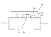
일실시예에 따른 발광소자 패키지(300)는 몸체(310)와, 상기 몸체(310)에 배치된 제1 리드 프레임(321) 및 제2 리드 프레임(322)과, 상기 몸체(310)에 배치되어 상기 제1 리드 프레임(321) 및 제2 리드 프레임(322)과 전기적으로 연결되는 상술한 실시예들에 따른 발광소자(100)와, 상기 캐비티에 형성된 몰딩부(340)를 포함한다. 상기 몸체(310)에는 캐비티가 형성될 수 있다.The light emitting
상기 몸체(310)는 실리콘 재질, 합성수지 재질, 또는 금속 재질을 포함하여 형성될 수 있다. 상기 몸체(310)가 금속 재질 등 도전성 물질로 이루어지면, 도시되지는 않았으나 상기 몸체(310)의 표면에 절연층이 코팅되어 상기 제1,2 리드 프레임(321, 322) 간의 전기적 단락을 방지할 수 있다.The
상기 제1 리드 프레임(321) 및 제2 리드 프레임(322)은 서로 전기적으로 분리되며, 상기 발광소자(100)에 전류를 공급한다. 또한, 상기 제1 리드 프레임(321) 및 제2 리드 프레임(322)은 상기 발광소자(100)에서 발생된 광을 반사시켜 광 효율을 증가시킬 수 있으며, 상기 발광소자(100)에서 발생된 열을 외부로 배출시킬 수도 있다.The
상기 발광소자(100)는 상기 몸체(310) 상에 배치되거나 상기 제1 리드 프레임(321) 또는 제2 리드 프레임(322) 상에 배치될 수 있다. 본 실시예에서는 제1 리드 프레임(321)과 발광소자(100)가 직접 통전되고, 제2 리드 프레임(322)과 상기 발광소자(100)는 와이어(330)를 통하여 연결되어 있다. 발광소자(100)는 와이어 본딩 방식 외에 플립칩 방식 또는 다이 본딩 방식 등에 의하여 리드 프레임(321, 322)과 연결될 수 있다.The
상기 몰딩부(340)는 상기 발광소자(100)를 포위하여 보호할 수 있다. 또한, 상기 몰딩부(340) 상에는 형광체(350)가 포함되어, 상기 발광소자(100)로부터 방출되는 빛의 파장을 변화시킬 수 있다.The
형광체(350)는 가넷(Garnet)계 형광체, 실리케이트(Silicate)계 형광체, 니트라이드(Nitride)계 형광체, 또는 옥시니트라이드(Oxynitride)계 형광체를 포함할 수 있다.The
예를 들어, 상기 가넷계 형광체는 YAG(Y3Al5O12:Ce3+) 또는 TAG(Tb3Al5O12:Ce3+)일 수 있고, 상기 실리케이트계 형광체는 (Sr,Ba,Mg,Ca)2SiO4:Eu2+일 수 있고, 상기 니트라이드계 형광체는 SiN을 포함하는 CaAlSiN3:Eu2+일 수 있고, 상기 옥시니트라이드계 형광체는 SiON을 포함하는 Si6-xAlxOxN8-x:Eu2+(0<x<6)일 수 있다.For example, the garnet-base phosphor isYAG (Y 3 Al 5 O 12 : Ce 3 +) or TAG: may be a(Tb 3 Al 5 O 12 Ce 3 +), wherein the silicate-based phosphor is (Sr, Ba, Mg, Ca)2 SiO4 : Eu2+ , and the nitride phosphor may be CaAlSiN3 : Eu2+ containing SiN, and the oxynitride phosphor may be Si6-xAl x O x N 8 -x: Eu 2 + (0 <x <6) can be.
상기 발광소자(100)에서 방출된 제1 파장 영역의 광이 상기 형광체(350)에 의하여 여기되어 제2 파장 영역의 광으로 변환되고, 상기 제2 파장 영역의 광은 렌즈(미도시)를 통과하면서 광경로가 변경될 수 있다.The light of the first wavelength range emitted from the
실시예에 따른 발광소자 패키지는 복수 개가 기판 상에 어레이되며, 상기 발광소자 패키지의 광 경로 상에 광학 부재인 도광판, 프리즘 시트, 확산 시트 등이 배치될 수 있다. 이러한 발광소자 패키지, 기판, 광학 부재는 라이트 유닛으로 기능할 수 있다. 또 다른 실시 예는 상술한 실시 예들에 기재된 반도체 발광소자 또는 발광소자 패키지를 포함하는 표시 장치, 지시 장치, 조명 시스템으로 구현될 수 있으며, 예를 들어, 조명 시스템은 램프, 가로등을 포함할 수 있다.A plurality of light emitting device packages according to embodiments may be arranged on a substrate, and a light guide plate, a prism sheet, a diffusion sheet, and the like may be disposed on the light path of the light emitting device package. Such a light emitting device package, a substrate, and an optical member can function as a light unit. Still another embodiment may be implemented as a display device, an indicating device, a lighting system including the semiconductor light emitting device or the light emitting device package described in the above embodiments, for example, the lighting system may include a lamp, a streetlight .
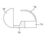
이하에서는 상술한 발광소자 또는 발광소자 패키지가 배치된 조명 시스템의 일실시예로서, 헤드램프와 백라이트 유닛을 설명한다.Hereinafter, the headlamp and the backlight unit will be described as an embodiment of the lighting system in which the above-described light emitting device or the light emitting device package is disposed.
도 16은 실시예들에 따른 발광소자 또는 발광소자 패키지가 배치된 헤드램프의 일실시예를 도시한 도면이다.16 is a view illustrating an embodiment of a headlamp in which a light emitting device or a light emitting device package according to embodiments is disposed.
도 16을 참조하면, 실시예들에 따른 발광소자 또는 발광소자 패키지가 배치된 발광 모듈(710)에서 방출된 빛이 리플렉터(720)와 쉐이드(730)에서 반사된 후 렌즈(740)를 투과하여 차체 전방을 향할 수 있다.16, the light emitted from the
상기 발광 모듈(710)은 회로기판 상에 발광소자가 복수 개로 탑재될 수 있으며, 이에 대해 한정하지 않는다.The
도 17은 실시예에 따른 발광소자 패키지가 배치된 표시장치의 일실시예를 도시한 도면이다.17 is a view illustrating a display device in which a light emitting device package according to an embodiment is disposed.
도 17을 참조하면, 실시예에 따른 표시장치(800)는 발광 모듈(830, 835)과, 바텀 커버(810) 상의 반사판(820)과, 상기 반사판(820)의 전방에 배치되며 상기 발광 모듈에서 방출되는 빛을 표시장치 전방으로 가이드하는 도광판(840)과, 상기 도광판(840)의 전방에 배치되는 제1 프리즘시트(850)와 제2 프리즘시트(860)와, 상기 제2 프리즘시트(860)의 전방에 배치되는 패널(870)과 상기 패널(870)의 전반에 배치되는 컬러필터(880)를 포함하여 이루어진다.17, the
발광 모듈은 회로 기판(830) 상의 상술한 발광소자 패키지(835)를 포함하여 이루어진다. 여기서, 회로 기판(830)은 PCB 등이 사용될 수 있고, 발광소자 패키지(835)는 도 15에서 설명한 바와 같다.The light emitting module includes the above-described light
상기 바텀 커버(810)는 표시 장치(800) 내의 구성 요소들을 수납할 수 있다. 상기 반사판(820)은 본 도면처럼 별도의 구성요소로 마련될 수도 있고, 상기 도광판(840)의 후면이나, 상기 바텀 커버(810)의 전면에 반사도가 높은 물질로 코팅되는 형태로 마련되는 것도 가능하다.The
여기서, 반사판(820)은 반사율이 높고 초박형으로 사용 가능한 소재를 사용할 수 있고, 폴리에틸렌 테레프탈레이트(PolyEthylene Terephtalate; PET)를 사용할 수 있다.Here, the
도광판(840)은 발광소자 패키지 모듈에서 방출되는 빛을 산란시켜 그 빛이 액정 표시 장치의 화면 전영역에 걸쳐 균일하게 분포되도록 한다. 따라서, 도광판(830)은 굴절률과 투과율이 좋은 재료로 이루어지는데, 폴리메틸메타크릴레이트(PolyMethylMethAcrylate; PMMA), 폴리카보네이트(PolyCarbonate; PC), 또는 폴리에틸렌(PolyEthylene; PE) 등으로 형성될 수 있다. 그리고, 도광판이 생략되어 반사시트(820) 위의 공간에서 빛이 전달되는 에어 가이드 방식도 가능하다.The
상기 제1 프리즘 시트(850)는 지지필름의 일면에, 투광성이면서 탄성을 갖는 중합체 재료로 형성되는데, 상기 중합체는 복수 개의 입체구조가 반복적으로 형성된 프리즘층을 가질 수 있다. 여기서, 상기 복수 개의 패턴은 도시된 바와 같이 마루와 골이 반복적으로 스트라이프 타입으로 구비될 수 있다.The
상기 제2 프리즘 시트(860)에서 지지필름 일면의 마루와 골의 방향은, 상기 제1 프리즘 시트(850) 내의 지지필름 일면의 마루와 골의 방향과 수직할 수 있다. 이는 발광 모듈과 반사시트로부터 전달된 빛을 상기 패널(870)의 전방향으로 고르게 분산하기 위함이다.In the
본 실시예에서 상기 제1 프리즘시트(850)과 제2 프리즘시트(860)가 광학시트를 이루는데, 상기 광학시트는 다른 조합 예를 들어, 마이크로 렌즈 어레이로 이루어지거나 확산시트와 마이크로 렌즈 어레이의 조합 또는 하나의 프리즘 시트와 마이크로 렌즈 어레이의 조합 등으로 이루어질 수 있다.In the present embodiment, the
상기 패널(870)은 액정 표시 패널(Liquid crystal display)가 배치될 수 있는데, 액정 표시 패널(860) 외에 광원을 필요로 하는 다른 종류의 디스플레이 장치가 구비될 수 있다.A liquid crystal display (LCD) panel may be disposed on the
상기 패널(870)은, 유리 바디 사이에 액정이 위치하고 빛의 편광성을 이용하기 위해 편광판을 양 유리바디에 올린 상태로 되어있다. 여기서, 액정은 액체와 고체의 중간적인 특성을 가지는데, 액체처럼 유동성을 갖는 유기분자인 액정이 결정처럼 규칙적으로 배열된 상태를 갖는 것으로, 상기 분자 배열이 외부 전계에 의해 변화되는 성질을 이용하여 화상을 표시한다.In the
표시장치에 사용되는 액정 표시 패널은, 액티브 매트릭스(Active Matrix) 방식으로서, 각 화소에 공급되는 전압을 조절하는 스위치로서 트랜지스터를 사용한다.A liquid crystal display panel used in a display device is an active matrix type, and a transistor is used as a switch for controlling a voltage supplied to each pixel.
상기 패널(870)의 전면에는 컬러 필터(880)가 구비되어 상기 패널(870)에서 투사된 빛을, 각각의 화소마다 적색과 녹색 및 청색의 빛만을 투과하므로 화상을 표현할 수 있다.A
이상과 같이 실시예는 비록 한정된 실시예와 도면에 의해 설명되었으나, 본 발명은 상기의 실시예에 한정되는 것은 아니며, 본 발명이 속하는 분야에서 통상의 지식을 가진 자라면 이러한 기재로부터 다양한 수정 및 변형이 가능하다.While the present invention has been particularly shown and described with reference to exemplary embodiments thereof, it is to be understood that the invention is not limited to the disclosed embodiments, but, on the contrary, This is possible.
그러므로, 본 발명의 범위는 설명된 실시예에 국한되어 정해져서는 아니되며, 후술하는 특허청구범위뿐 아니라 이 특허청구범위와 균등한 것들에 의해 정해져야 한다.Therefore, the scope of the present invention should not be limited to the described embodiments, but should be determined by the equivalents of the claims, as well as the claims.
100: 발광소자 110: 기판
120: 발광 구조물 122: 제1 도전형 반도체층
124: 활성층 126: 제2 도전형 반도체층
126a: 정공 주입층 200: 전자 차단층
200-1: 제1 영역 200-2: 제2 영역
160: 제2 전극층 170: 채널층
180: 지지기판 190: 패시베이션층
310: 패키지 몸체 321, 322: 제1,2 리드 프레임
330: 와이어 340: 몰딩부
350: 형광체 710: 발광 모듈
720: 리플렉터 730: 쉐이드
800: 표시장치 810: 바텀 커버
820: 반사판 840: 도광판
850: 제1 프리즘시트 860: 제2 프리즘시트
870: 패널 880: 컬러필터100: light emitting device 110: substrate
120: light emitting structure 122: first conductivity type semiconductor layer
124: active layer 126: second conductivity type semiconductor layer
126a: Hole injection layer 200: Electron barrier layer
200-1: first region 200-2: second region
160: second electrode layer 170: channel layer
180: support substrate 190: passivation layer
310:
330: wire 340: molding part
350: phosphor 710: light emitting module
720: Reflector 730: Shade
800: Display device 810: Bottom cover
820: reflector 840: light guide plate
850: first prism sheet 860: second prism sheet
870: Panel 880: Color filter
Claims (13)
Translated fromKorean제2 도전형 반도체층; 및
상기 제1 도전형 반도체층과 상기 제2 도전형 반도체층 사이에 위치하고, 상기 활성층에 인접하여 전자 차단층을 포함하는 제2 도전형 반도체층;을 포함하고,
상기 전자 차단층은 장벽층 및 상기 장벽층보다 에너지 밴드갭이 작은 우물층의 페어 구조를 복수 개 포함하며,
상기 전자 차단층은 상기 활성층에 인접하고 장벽층 및 우물층의 페어 구조를 적어도 하나 포함하는 제1 영역과, 상기 제1 영역 상에 위치하고 장벽층 및 우물층의 페어 구조를 적어도 하나 포함하는 제2 영역을 포함하고, 상기 제1 영역에 속하는 우물층의 두께가 상기 제2 영역에 속하는 우물층의 두께보다 두꺼운 발광소자.A first conductive semiconductor layer;
A second conductivity type semiconductor layer; And
And a second conductive type semiconductor layer disposed between the first conductive type semiconductor layer and the second conductive type semiconductor layer and including an electron blocking layer adjacent to the active layer,
Wherein the electron blocking layer includes a plurality of pairs of a barrier layer and a well layer having a smaller energy bandgap than the barrier layer,
Wherein the electron blocking layer includes a first region adjacent to the active layer and including at least one pair structure of a barrier layer and a well layer, and a second region located on the first region and including at least one pair structure of a barrier layer and a well layer. Wherein the thickness of the well layer belonging to the first region is thicker than the thickness of the well layer belonging to the second region.
상기 제1 영역에 속하는 복수 개의 우물층은 상기 활성층에서 멀어지는 방향으로 갈수록 두께가 감소하는 발광소자.The method according to claim 1,
Wherein a plurality of well layers belonging to the first region are reduced in thickness in a direction away from the active layer.
상기 제1 영역에 속하는 복수 개의 우물층 중에서 상기 활성층에 가장 인접한 우물층의 두께가 가장 두꺼운 발광소자.The method according to claim 1,
Wherein a well layer closest to the active layer is thickest among a plurality of well layers belonging to the first region.
상기 전자 차단층에 속하는 복수 개의 우물층은 상기 활성층에서 멀어지는 방향으로 갈수록 두께가 감소하는 발광소자.The method according to claim 1,
Wherein the plurality of well layers belonging to the electron blocking layer are reduced in thickness in a direction away from the active layer.
상기 제1 영역에 속하는 장벽층의 두께가 상기 제2 영역에 속하는 장벽층의 두께보다 두꺼운 발광소자.The method according to claim 1,
Wherein the thickness of the barrier layer belonging to the first region is thicker than the thickness of the barrier layer belonging to the second region.
상기 제1 영역에 속하는 복수 개의 장벽층은 상기 활성층에서 멀어지는 방향으로 갈수록 두께가 감소하는 발광소자.The method according to claim 1,
Wherein a plurality of barrier layers belonging to the first region are reduced in thickness in a direction away from the active layer.
상기 제1 영역에 속하는 복수 개의 장벽층 중에서 상기 활성층에 가장 인접한 장벽층의 두께가 가장 두꺼운 발광소자.The method according to claim 1,
Wherein a thickness of the barrier layer closest to the active layer among the plurality of barrier layers belonging to the first region is thickest.
상기 전자 차단층에 속하는 복수 개의 장벽층은 상기 활성층에서 멀어지는 방향으로 갈수록 두께가 감소하는 발광소자.The method according to claim 1,
Wherein a thickness of the plurality of barrier layers belonging to the electron blocking layer decreases in a direction away from the active layer.
상기 전자 차단층에 속하는 복수 개의 우물층 중에서 상기 활성층에 가장 인접한 적어도 하나의 우물층은 In을 포함하여 이루어진 발광소자.The method according to claim 1,
And at least one well layer closest to the active layer among the plurality of well layers belonging to the electron blocking layer includes In.
상기 전자 차단층에 속하는 복수 개의 우물층 중에서 상기 활성층에 가장 인접한 적어도 하나의 우물층의 In 함량이 가장 높은 발광소자.The method according to claim 1,
Wherein at least one well layer closest to the active layer among the plurality of well layers belonging to the electron blocking layer has the highest In content.
상기 전자 차단층에 속하는 복수 개의 우물층 중에서 상기 활성층에 가장 인접한 적어도 하나의 우물층의 에너지 밴드갭이 가장 작은 발광소자.The method according to claim 1,
Wherein at least one well layer closest to the active layer among the plurality of well layers belonging to the electron blocking layer has the lowest energy band gap.
상기 제2 도전형 반도체층은 상기 활성층과 상기 전자 차단층 사이에 정공 주입층을 더 포함하는 발광소자.The method according to claim 1,
Wherein the second conductivity type semiconductor layer further comprises a hole injection layer between the active layer and the electron blocking layer.
상기 전자 차단층에 속하는 복수 개의 장벽층 및 복수 개의 우물층 중에서 상기 활성층에 가장 인접한 장벽층의 두께가 가장 두꺼운 발광소자.The method according to claim 1,
Wherein a thickness of the barrier layer closest to the active layer is the thickest among a plurality of barrier layers and a plurality of well layers belonging to the electron blocking layer.
Priority Applications (1)
| Application Number | Priority Date | Filing Date | Title |
|---|---|---|---|
| KR1020120123414AKR20140056929A (en) | 2012-11-02 | 2012-11-02 | Light emitting device |
Applications Claiming Priority (1)
| Application Number | Priority Date | Filing Date | Title |
|---|---|---|---|
| KR1020120123414AKR20140056929A (en) | 2012-11-02 | 2012-11-02 | Light emitting device |
Publications (1)
| Publication Number | Publication Date |
|---|---|
| KR20140056929Atrue KR20140056929A (en) | 2014-05-12 |
Family
ID=50887989
Family Applications (1)
| Application Number | Title | Priority Date | Filing Date |
|---|---|---|---|
| KR1020120123414ACeasedKR20140056929A (en) | 2012-11-02 | 2012-11-02 | Light emitting device |
Country Status (1)
| Country | Link |
|---|---|
| KR (1) | KR20140056929A (en) |
Cited By (1)
| Publication number | Priority date | Publication date | Assignee | Title |
|---|---|---|---|---|
| US10199540B2 (en) | 2015-01-12 | 2019-02-05 | Lg Innotek Co., Ltd. | Light emitting diode, light emitting diode package including same, and lighting system including same |
- 2012
- 2012-11-02KRKR1020120123414Apatent/KR20140056929A/ennot_activeCeased
Cited By (1)
| Publication number | Priority date | Publication date | Assignee | Title |
|---|---|---|---|---|
| US10199540B2 (en) | 2015-01-12 | 2019-02-05 | Lg Innotek Co., Ltd. | Light emitting diode, light emitting diode package including same, and lighting system including same |
Similar Documents
| Publication | Publication Date | Title |
|---|---|---|
| KR101827975B1 (en) | Light emitting device | |
| KR101941033B1 (en) | Light emitting device | |
| KR101908657B1 (en) | Light emitting device | |
| KR20140059985A (en) | Light emitting device | |
| EP2696375A2 (en) | Light emitting diode | |
| KR101998763B1 (en) | Light emittng device | |
| KR101915213B1 (en) | Light emitting device | |
| KR101954202B1 (en) | Light emitting device and illuminating system including the same | |
| KR101922529B1 (en) | Light emitting device | |
| KR101963220B1 (en) | Light emitting device | |
| KR101991032B1 (en) | Light emitting device | |
| KR101929933B1 (en) | Light emitting device and lighting system including the device | |
| KR20140046162A (en) | Light emitting device | |
| KR20140056930A (en) | Light emitting device | |
| KR102050053B1 (en) | Light emitting device | |
| KR102007401B1 (en) | Light emitting device | |
| KR20140092092A (en) | Light emitting device | |
| KR101915212B1 (en) | Light emitting device | |
| KR101911865B1 (en) | Light emitting device | |
| KR20140056929A (en) | Light emitting device | |
| KR101960791B1 (en) | Light emitting device | |
| KR101963222B1 (en) | Light emitting device | |
| KR20140056931A (en) | Light emitting device | |
| KR20140019509A (en) | Light emitting device | |
| KR101983775B1 (en) | Light emitting device |
Legal Events
| Date | Code | Title | Description |
|---|---|---|---|
| PA0109 | Patent application | Patent event code:PA01091R01D Comment text:Patent Application Patent event date:20121102 | |
| PG1501 | Laying open of application | ||
| PA0201 | Request for examination | Patent event code:PA02012R01D Patent event date:20171027 Comment text:Request for Examination of Application Patent event code:PA02011R01I Patent event date:20121102 Comment text:Patent Application | |
| E902 | Notification of reason for refusal | ||
| PE0902 | Notice of grounds for rejection | Comment text:Notification of reason for refusal Patent event date:20180918 Patent event code:PE09021S01D | |
| E601 | Decision to refuse application | ||
| PE0601 | Decision on rejection of patent | Patent event date:20190328 Comment text:Decision to Refuse Application Patent event code:PE06012S01D Patent event date:20180918 Comment text:Notification of reason for refusal Patent event code:PE06011S01I |