KR20140042728A - Phosphor adhesive sheet, optical semiconductor element-phosphor layer pressure-sensitive adhesive body, and optical semiconductor device - Google Patents
Phosphor adhesive sheet, optical semiconductor element-phosphor layer pressure-sensitive adhesive body, and optical semiconductor deviceDownload PDFInfo
- Publication number
- KR20140042728A KR20140042728AKR1020130115088AKR20130115088AKR20140042728AKR 20140042728 AKR20140042728 AKR 20140042728AKR 1020130115088 AKR1020130115088 AKR 1020130115088AKR 20130115088 AKR20130115088 AKR 20130115088AKR 20140042728 AKR20140042728 AKR 20140042728A
- Authority
- KR
- South Korea
- Prior art keywords
- pressure
- phosphor layer
- layer
- phosphor
- fluorescent
- Prior art date
- Legal status (The legal status is an assumption and is not a legal conclusion. Google has not performed a legal analysis and makes no representation as to the accuracy of the status listed.)
- Withdrawn
Links
- 239000000853adhesiveSubstances0.000titleclaimsabstractdescription105
- 230000001070adhesive effectEffects0.000titleclaimsabstractdescription105
- 239000004820Pressure-sensitive adhesiveSubstances0.000titleclaimsabstractdescription85
- OAICVXFJPJFONN-UHFFFAOYSA-NPhosphorusChemical compound[P]OAICVXFJPJFONN-UHFFFAOYSA-N0.000titleclaimsdescription128
- 239000004065semiconductorSubstances0.000titleclaimsdescription46
- 230000003287optical effectEffects0.000titleclaimsdescription44
- 239000010410layerSubstances0.000claimsabstractdescription174
- 229920001296polysiloxanePolymers0.000claimsabstractdescription62
- 239000012790adhesive layerSubstances0.000claimsabstractdescription53
- 239000000203mixtureSubstances0.000claimsabstractdescription45
- 239000000126substanceSubstances0.000claimsabstractdescription37
- 239000000758substrateSubstances0.000claimsdescription42
- 239000012298atmosphereSubstances0.000claimsdescription32
- 239000000919ceramicSubstances0.000claimsdescription27
- 239000011347resinSubstances0.000claimsdescription23
- 229920005989resinPolymers0.000claimsdescription23
- 238000000034methodMethods0.000claimsdescription22
- 238000005538encapsulationMethods0.000claimsdescription7
- -1CaAlSiN 3 : EuInorganic materials0.000description31
- 230000000052comparative effectEffects0.000description16
- 238000002360preparation methodMethods0.000description16
- 239000004793PolystyreneSubstances0.000description15
- 239000011342resin compositionSubstances0.000description14
- 238000004519manufacturing processMethods0.000description13
- 229920002050silicone resinPolymers0.000description11
- YXFVVABEGXRONW-UHFFFAOYSA-NTolueneChemical compoundCC1=CC=CC=C1YXFVVABEGXRONW-UHFFFAOYSA-N0.000description9
- 239000002994raw materialSubstances0.000description9
- 125000005372silanol groupChemical group0.000description8
- OMPJBNCRMGITSC-UHFFFAOYSA-NBenzoylperoxideChemical classC=1C=CC=CC=1C(=O)OOC(=O)C1=CC=CC=C1OMPJBNCRMGITSC-UHFFFAOYSA-N0.000description7
- 235000019400benzoyl peroxideNutrition0.000description7
- 125000002496methyl groupChemical group[H]C([H])([H])*0.000description7
- 238000002156mixingMethods0.000description7
- NIXOWILDQLNWCW-UHFFFAOYSA-Nacrylic acid groupChemical groupC(C=C)(=O)ONIXOWILDQLNWCW-UHFFFAOYSA-N0.000description6
- 125000001183hydrocarbyl groupChemical group0.000description6
- 239000002904solventSubstances0.000description6
- JNDMLEXHDPKVFC-UHFFFAOYSA-Naluminum;oxygen(2-);yttrium(3+)Chemical compound[O-2].[O-2].[O-2].[Al+3].[Y+3]JNDMLEXHDPKVFC-UHFFFAOYSA-N0.000description5
- 239000003054catalystSubstances0.000description5
- 239000002245particleSubstances0.000description5
- 229920001721polyimidePolymers0.000description5
- 238000007789sealingMethods0.000description5
- 229910052710siliconInorganic materials0.000description5
- 229910019901yttrium aluminum garnetInorganic materials0.000description5
- NLBJAOHLJABDAU-UHFFFAOYSA-N(3-methylbenzoyl) 3-methylbenzenecarboperoxoateChemical compoundCC1=CC=CC(C(=O)OOC(=O)C=2C=C(C)C=CC=2)=C1NLBJAOHLJABDAU-UHFFFAOYSA-N0.000description4
- QZYOLNVEVYIPHV-UHFFFAOYSA-N1-methyl-3-(3-methylphenyl)peroxybenzeneChemical compoundCC1=CC=CC(OOC=2C=C(C)C=CC=2)=C1QZYOLNVEVYIPHV-UHFFFAOYSA-N0.000description4
- XUIMIQQOPSSXEZ-UHFFFAOYSA-NSiliconChemical group[Si]XUIMIQQOPSSXEZ-UHFFFAOYSA-N0.000description4
- 238000004026adhesive bondingMethods0.000description4
- 125000004122cyclic groupChemical group0.000description4
- 235000013870dimethyl polysiloxaneNutrition0.000description4
- 239000004205dimethyl polysiloxaneSubstances0.000description4
- 239000000463materialSubstances0.000description4
- 229920000435poly(dimethylsiloxane)Polymers0.000description4
- 239000000843powderSubstances0.000description4
- SCPYDCQAZCOKTP-UHFFFAOYSA-NsilanolChemical compound[SiH3]OSCPYDCQAZCOKTP-UHFFFAOYSA-N0.000description4
- 239000007787solidSubstances0.000description4
- 239000002966varnishSubstances0.000description4
- 229910052684CeriumInorganic materials0.000description3
- 229910010293ceramic materialInorganic materials0.000description3
- 238000006243chemical reactionMethods0.000description3
- 238000000576coating methodMethods0.000description3
- 238000013329compoundingMethods0.000description3
- 239000004020conductorSubstances0.000description3
- 230000000694effectsEffects0.000description3
- 150000002978peroxidesChemical class0.000description3
- 125000001997phenyl groupChemical group[H]C1=C([H])C([H])=C(*)C([H])=C1[H]0.000description3
- 239000010703siliconSubstances0.000description3
- 238000005245sinteringMethods0.000description3
- 229910052727yttriumInorganic materials0.000description3
- 229920002799BoPETPolymers0.000description2
- 125000000041C6-C10 aryl groupChemical group0.000description2
- 229910052693EuropiumInorganic materials0.000description2
- PXHVJJICTQNCMI-UHFFFAOYSA-NNickelChemical compound[Ni]PXHVJJICTQNCMI-UHFFFAOYSA-N0.000description2
- 229910004283SiO 4Inorganic materials0.000description2
- 125000000217alkyl groupChemical group0.000description2
- 229910052782aluminiumInorganic materials0.000description2
- 125000002029aromatic hydrocarbon groupChemical group0.000description2
- 239000011230binding agentSubstances0.000description2
- 125000004432carbon atomChemical groupC*0.000description2
- 239000011248coating agentSubstances0.000description2
- 229910052802copperInorganic materials0.000description2
- 239000010949copperSubstances0.000description2
- 230000006866deteriorationEffects0.000description2
- 230000005284excitationEffects0.000description2
- 230000020169heat generationEffects0.000description2
- 238000010438heat treatmentMethods0.000description2
- 230000007774longtermEffects0.000description2
- 238000005259measurementMethods0.000description2
- HMMGMWAXVFQUOA-UHFFFAOYSA-NoctamethylcyclotetrasiloxaneChemical compoundC[Si]1(C)O[Si](C)(C)O[Si](C)(C)O[Si](C)(C)O1HMMGMWAXVFQUOA-UHFFFAOYSA-N0.000description2
- 229930195734saturated hydrocarbonNatural products0.000description2
- 239000002002slurrySubstances0.000description2
- VWQVUPCCIRVNHF-UHFFFAOYSA-Nyttrium atomChemical compound[Y]VWQVUPCCIRVNHF-UHFFFAOYSA-N0.000description2
- 125000004169(C1-C6) alkyl groupChemical group0.000description1
- NIXOWILDQLNWCW-UHFFFAOYSA-MAcrylateChemical compound[O-]C(=O)C=CNIXOWILDQLNWCW-UHFFFAOYSA-M0.000description1
- 239000004925Acrylic resinSubstances0.000description1
- 229920000178Acrylic resinPolymers0.000description1
- 229910016066BaSiInorganic materials0.000description1
- 229910004709CaSiInorganic materials0.000description1
- 229910004706CaSi2Inorganic materials0.000description1
- RYGMFSIKBFXOCR-UHFFFAOYSA-NCopperChemical compound[Cu]RYGMFSIKBFXOCR-UHFFFAOYSA-N0.000description1
- XMSXQFUHVRWGNA-UHFFFAOYSA-NDecamethylcyclopentasiloxaneChemical compoundC[Si]1(C)O[Si](C)(C)O[Si](C)(C)O[Si](C)(C)O[Si](C)(C)O1XMSXQFUHVRWGNA-UHFFFAOYSA-N0.000description1
- KRHYYFGTRYWZRS-UHFFFAOYSA-MFluoride anionChemical compound[F-]KRHYYFGTRYWZRS-UHFFFAOYSA-M0.000description1
- 229910052688GadoliniumInorganic materials0.000description1
- 101100476480Mus musculus S100a8 geneProteins0.000description1
- BPQQTUXANYXVAA-UHFFFAOYSA-NOrthosilicateChemical compound[O-][Si]([O-])([O-])[O-]BPQQTUXANYXVAA-UHFFFAOYSA-N0.000description1
- 229910003564SiAlONInorganic materials0.000description1
- 229910020175SiOHInorganic materials0.000description1
- BQCADISMDOOEFD-UHFFFAOYSA-NSilverChemical compound[Ag]BQCADISMDOOEFD-UHFFFAOYSA-N0.000description1
- 229910003668SrAlInorganic materials0.000description1
- 229910004122SrSiInorganic materials0.000description1
- UCKMPCXJQFINFW-UHFFFAOYSA-NSulphideChemical compound[S-2]UCKMPCXJQFINFW-UHFFFAOYSA-N0.000description1
- 229910052771TerbiumInorganic materials0.000description1
- GWEVSGVZZGPLCZ-UHFFFAOYSA-NTitan oxideChemical compoundO=[Ti]=OGWEVSGVZZGPLCZ-UHFFFAOYSA-N0.000description1
- 238000007259addition reactionMethods0.000description1
- 239000000654additiveSubstances0.000description1
- 239000002671adjuvantSubstances0.000description1
- 125000003545alkoxy groupChemical group0.000description1
- 150000004645aluminatesChemical class0.000description1
- PNEYBMLMFCGWSK-UHFFFAOYSA-Naluminium oxideInorganic materials[O-2].[O-2].[O-2].[Al+3].[Al+3]PNEYBMLMFCGWSK-UHFFFAOYSA-N0.000description1
- 150000004945aromatic hydrocarbonsChemical class0.000description1
- 125000003118aryl groupChemical group0.000description1
- 125000000484butyl groupChemical group[H]C([*])([H])C([H])([H])C([H])([H])C([H])([H])[H]0.000description1
- GWXLDORMOJMVQZ-UHFFFAOYSA-NceriumChemical compound[Ce]GWXLDORMOJMVQZ-UHFFFAOYSA-N0.000description1
- 229910000420cerium oxideInorganic materials0.000description1
- 239000002131composite materialSubstances0.000description1
- 238000002788crimpingMethods0.000description1
- 239000013078crystalSubstances0.000description1
- 125000000753cycloalkyl groupChemical group0.000description1
- 125000000113cyclohexyl groupChemical group[H]C1([H])C([H])([H])C([H])([H])C([H])(*)C([H])([H])C1([H])[H]0.000description1
- 125000001511cyclopentyl groupChemical group[H]C1([H])C([H])([H])C([H])([H])C([H])(*)C1([H])[H]0.000description1
- 230000018044dehydrationEffects0.000description1
- 238000006297dehydration reactionMethods0.000description1
- KPUWHANPEXNPJT-UHFFFAOYSA-NdisiloxaneChemical class[SiH3]O[SiH3]KPUWHANPEXNPJT-UHFFFAOYSA-N0.000description1
- 239000002270dispersing agentSubstances0.000description1
- 239000012153distilled waterSubstances0.000description1
- 238000007606doctor blade methodMethods0.000description1
- 239000003822epoxy resinSubstances0.000description1
- 125000001495ethyl groupChemical group[H]C([H])([H])C([H])([H])*0.000description1
- OGPBJKLSAFTDLK-UHFFFAOYSA-Neuropium atomChemical compound[Eu]OGPBJKLSAFTDLK-UHFFFAOYSA-N0.000description1
- 238000011156evaluationMethods0.000description1
- 229910052733galliumInorganic materials0.000description1
- 239000002223garnetSubstances0.000description1
- 238000005227gel permeation chromatographyMethods0.000description1
- 239000011521glassSubstances0.000description1
- PCHJSUWPFVWCPO-UHFFFAOYSA-NgoldChemical compound[Au]PCHJSUWPFVWCPO-UHFFFAOYSA-N0.000description1
- 229910052737goldInorganic materials0.000description1
- 239000010931goldSubstances0.000description1
- 239000004519greaseSubstances0.000description1
- 238000000227grindingMethods0.000description1
- HTDJPCNNEPUOOQ-UHFFFAOYSA-NhexamethylcyclotrisiloxaneChemical compoundC[Si]1(C)O[Si](C)(C)O[Si](C)(C)O1HTDJPCNNEPUOOQ-UHFFFAOYSA-N0.000description1
- 125000004051hexyl groupChemical group[H]C([H])([H])C([H])([H])C([H])([H])C([H])([H])C([H])([H])C([H])([H])*0.000description1
- 125000000959isobutyl groupChemical group[H]C([H])([H])C([H])(C([H])([H])[H])C([H])([H])*0.000description1
- 125000001449isopropyl groupChemical group[H]C([H])([H])C([H])(*)C([H])([H])[H]0.000description1
- 239000007788liquidSubstances0.000description1
- 238000004020luminiscence typeMethods0.000description1
- 229910052748manganeseInorganic materials0.000description1
- 239000011159matrix materialSubstances0.000description1
- 229910052751metalInorganic materials0.000description1
- 239000002184metalSubstances0.000description1
- 229910044991metal oxideInorganic materials0.000description1
- 150000004706metal oxidesChemical class0.000description1
- 229910052976metal sulfideInorganic materials0.000description1
- 125000000956methoxy groupChemical group[H]C([H])([H])O*0.000description1
- 125000001624naphthyl groupChemical group0.000description1
- 229910052759nickelInorganic materials0.000description1
- 150000004767nitridesChemical class0.000description1
- 125000000962organic groupChemical group0.000description1
- 150000001451organic peroxidesChemical class0.000description1
- 125000005375organosiloxane groupChemical group0.000description1
- TWNQGVIAIRXVLR-UHFFFAOYSA-Noxo(oxoalumanyloxy)alumaneChemical compoundO=[Al]O[Al]=OTWNQGVIAIRXVLR-UHFFFAOYSA-N0.000description1
- BMMGVYCKOGBVEV-UHFFFAOYSA-Noxo(oxoceriooxy)ceriumChemical compound[Ce]=O.O=[Ce]=OBMMGVYCKOGBVEV-UHFFFAOYSA-N0.000description1
- SIWVEOZUMHYXCS-UHFFFAOYSA-Noxo(oxoyttriooxy)yttriumChemical compoundO=[Y]O[Y]=OSIWVEOZUMHYXCS-UHFFFAOYSA-N0.000description1
- 125000001147pentyl groupChemical groupC(CCCC)*0.000description1
- 239000004014plasticizerSubstances0.000description1
- 238000005498polishingMethods0.000description1
- 229920001921poly-methyl-phenyl-siloxanePolymers0.000description1
- 229920000647polyepoxidePolymers0.000description1
- 239000009719polyimide resinSubstances0.000description1
- 229920000642polymerPolymers0.000description1
- 229920002223polystyrenePolymers0.000description1
- 125000001436propyl groupChemical group[H]C([*])([H])C([H])([H])C([H])([H])[H]0.000description1
- 229910052761rare earth metalInorganic materials0.000description1
- 239000003566sealing materialSubstances0.000description1
- 229920002379silicone rubberPolymers0.000description1
- 229910052709silverInorganic materials0.000description1
- 239000004332silverSubstances0.000description1
- 229910002076stabilized zirconiaInorganic materials0.000description1
- 238000003756stirringMethods0.000description1
- 238000009823thermal laminationMethods0.000description1
- 238000001931thermographyMethods0.000description1
- 229920001187thermosetting polymerPolymers0.000description1
- OGIDPMRJRNCKJF-UHFFFAOYSA-Ntitanium oxideInorganic materials[Ti]=OOGIDPMRJRNCKJF-UHFFFAOYSA-N0.000description1
- XLYOFNOQVPJJNP-UHFFFAOYSA-NwaterChemical compoundOXLYOFNOQVPJJNP-UHFFFAOYSA-N0.000description1
- 239000003232water-soluble binding agentSubstances0.000description1
Images


Classifications
- C—CHEMISTRY; METALLURGY
- C09—DYES; PAINTS; POLISHES; NATURAL RESINS; ADHESIVES; COMPOSITIONS NOT OTHERWISE PROVIDED FOR; APPLICATIONS OF MATERIALS NOT OTHERWISE PROVIDED FOR
- C09J—ADHESIVES; NON-MECHANICAL ASPECTS OF ADHESIVE PROCESSES IN GENERAL; ADHESIVE PROCESSES NOT PROVIDED FOR ELSEWHERE; USE OF MATERIALS AS ADHESIVES
- C09J7/00—Adhesives in the form of films or foils
- C09J7/30—Adhesives in the form of films or foils characterised by the adhesive composition
- C09J7/38—Pressure-sensitive adhesives [PSA]
- C09J7/381—Pressure-sensitive adhesives [PSA] based on macromolecular compounds obtained by reactions involving only carbon-to-carbon unsaturated bonds
- B—PERFORMING OPERATIONS; TRANSPORTING
- B32—LAYERED PRODUCTS
- B32B—LAYERED PRODUCTS, i.e. PRODUCTS BUILT-UP OF STRATA OF FLAT OR NON-FLAT, e.g. CELLULAR OR HONEYCOMB, FORM
- B32B18/00—Layered products essentially comprising ceramics, e.g. refractory products
- C—CHEMISTRY; METALLURGY
- C09—DYES; PAINTS; POLISHES; NATURAL RESINS; ADHESIVES; COMPOSITIONS NOT OTHERWISE PROVIDED FOR; APPLICATIONS OF MATERIALS NOT OTHERWISE PROVIDED FOR
- C09J—ADHESIVES; NON-MECHANICAL ASPECTS OF ADHESIVE PROCESSES IN GENERAL; ADHESIVE PROCESSES NOT PROVIDED FOR ELSEWHERE; USE OF MATERIALS AS ADHESIVES
- C09J183/00—Adhesives based on macromolecular compounds obtained by reactions forming in the main chain of the macromolecule a linkage containing silicon, with or without sulfur, nitrogen, oxygen, or carbon only; Adhesives based on derivatives of such polymers
- C09J183/04—Polysiloxanes
- C09J183/06—Polysiloxanes containing silicon bound to oxygen-containing groups
- C—CHEMISTRY; METALLURGY
- C09—DYES; PAINTS; POLISHES; NATURAL RESINS; ADHESIVES; COMPOSITIONS NOT OTHERWISE PROVIDED FOR; APPLICATIONS OF MATERIALS NOT OTHERWISE PROVIDED FOR
- C09J—ADHESIVES; NON-MECHANICAL ASPECTS OF ADHESIVE PROCESSES IN GENERAL; ADHESIVE PROCESSES NOT PROVIDED FOR ELSEWHERE; USE OF MATERIALS AS ADHESIVES
- C09J7/00—Adhesives in the form of films or foils
- C09J7/20—Adhesives in the form of films or foils characterised by their carriers
- C09J7/22—Plastics; Metallised plastics
- C—CHEMISTRY; METALLURGY
- C09—DYES; PAINTS; POLISHES; NATURAL RESINS; ADHESIVES; COMPOSITIONS NOT OTHERWISE PROVIDED FOR; APPLICATIONS OF MATERIALS NOT OTHERWISE PROVIDED FOR
- C09J—ADHESIVES; NON-MECHANICAL ASPECTS OF ADHESIVE PROCESSES IN GENERAL; ADHESIVE PROCESSES NOT PROVIDED FOR ELSEWHERE; USE OF MATERIALS AS ADHESIVES
- C09J7/00—Adhesives in the form of films or foils
- C09J7/20—Adhesives in the form of films or foils characterised by their carriers
- C09J7/29—Laminated material
- C—CHEMISTRY; METALLURGY
- C09—DYES; PAINTS; POLISHES; NATURAL RESINS; ADHESIVES; COMPOSITIONS NOT OTHERWISE PROVIDED FOR; APPLICATIONS OF MATERIALS NOT OTHERWISE PROVIDED FOR
- C09J—ADHESIVES; NON-MECHANICAL ASPECTS OF ADHESIVE PROCESSES IN GENERAL; ADHESIVE PROCESSES NOT PROVIDED FOR ELSEWHERE; USE OF MATERIALS AS ADHESIVES
- C09J7/00—Adhesives in the form of films or foils
- C09J7/30—Adhesives in the form of films or foils characterised by the adhesive composition
- C09J7/38—Pressure-sensitive adhesives [PSA]
- C—CHEMISTRY; METALLURGY
- C09—DYES; PAINTS; POLISHES; NATURAL RESINS; ADHESIVES; COMPOSITIONS NOT OTHERWISE PROVIDED FOR; APPLICATIONS OF MATERIALS NOT OTHERWISE PROVIDED FOR
- C09J—ADHESIVES; NON-MECHANICAL ASPECTS OF ADHESIVE PROCESSES IN GENERAL; ADHESIVE PROCESSES NOT PROVIDED FOR ELSEWHERE; USE OF MATERIALS AS ADHESIVES
- C09J7/00—Adhesives in the form of films or foils
- C09J7/40—Adhesives in the form of films or foils characterised by release liners
- C—CHEMISTRY; METALLURGY
- C09—DYES; PAINTS; POLISHES; NATURAL RESINS; ADHESIVES; COMPOSITIONS NOT OTHERWISE PROVIDED FOR; APPLICATIONS OF MATERIALS NOT OTHERWISE PROVIDED FOR
- C09K—MATERIALS FOR MISCELLANEOUS APPLICATIONS, NOT PROVIDED FOR ELSEWHERE
- C09K11/00—Luminescent, e.g. electroluminescent, chemiluminescent materials
- C09K11/02—Use of particular materials as binders, particle coatings or suspension media therefor
- C09K11/025—Use of particular materials as binders, particle coatings or suspension media therefor non-luminescent particle coatings or suspension media
- H—ELECTRICITY
- H10—SEMICONDUCTOR DEVICES; ELECTRIC SOLID-STATE DEVICES NOT OTHERWISE PROVIDED FOR
- H10H—INORGANIC LIGHT-EMITTING SEMICONDUCTOR DEVICES HAVING POTENTIAL BARRIERS
- H10H20/00—Individual inorganic light-emitting semiconductor devices having potential barriers, e.g. light-emitting diodes [LED]
- H10H20/80—Constructional details
- H10H20/84—Coatings, e.g. passivation layers or antireflective coatings
- H—ELECTRICITY
- H10—SEMICONDUCTOR DEVICES; ELECTRIC SOLID-STATE DEVICES NOT OTHERWISE PROVIDED FOR
- H10H—INORGANIC LIGHT-EMITTING SEMICONDUCTOR DEVICES HAVING POTENTIAL BARRIERS
- H10H20/00—Individual inorganic light-emitting semiconductor devices having potential barriers, e.g. light-emitting diodes [LED]
- H10H20/80—Constructional details
- H10H20/85—Packages
- H10H20/851—Wavelength conversion means
- H10H20/8511—Wavelength conversion means characterised by their material, e.g. binder
- H10H20/8512—Wavelength conversion materials
- H—ELECTRICITY
- H10—SEMICONDUCTOR DEVICES; ELECTRIC SOLID-STATE DEVICES NOT OTHERWISE PROVIDED FOR
- H10H—INORGANIC LIGHT-EMITTING SEMICONDUCTOR DEVICES HAVING POTENTIAL BARRIERS
- H10H20/00—Individual inorganic light-emitting semiconductor devices having potential barriers, e.g. light-emitting diodes [LED]
- H10H20/80—Constructional details
- H10H20/85—Packages
- H10H20/851—Wavelength conversion means
- H10H20/8514—Wavelength conversion means characterised by their shape, e.g. plate or foil
- H—ELECTRICITY
- H10—SEMICONDUCTOR DEVICES; ELECTRIC SOLID-STATE DEVICES NOT OTHERWISE PROVIDED FOR
- H10H—INORGANIC LIGHT-EMITTING SEMICONDUCTOR DEVICES HAVING POTENTIAL BARRIERS
- H10H20/00—Individual inorganic light-emitting semiconductor devices having potential barriers, e.g. light-emitting diodes [LED]
- H10H20/80—Constructional details
- H10H20/85—Packages
- H10H20/851—Wavelength conversion means
- H10H20/8515—Wavelength conversion means not being in contact with the bodies
- C—CHEMISTRY; METALLURGY
- C04—CEMENTS; CONCRETE; ARTIFICIAL STONE; CERAMICS; REFRACTORIES
- C04B—LIME, MAGNESIA; SLAG; CEMENTS; COMPOSITIONS THEREOF, e.g. MORTARS, CONCRETE OR LIKE BUILDING MATERIALS; ARTIFICIAL STONE; CERAMICS; REFRACTORIES; TREATMENT OF NATURAL STONE
- C04B2235/00—Aspects relating to ceramic starting mixtures or sintered ceramic products
- C04B2235/65—Aspects relating to heat treatments of ceramic bodies such as green ceramics or pre-sintered ceramics, e.g. burning, sintering or melting processes
- C04B2235/656—Aspects relating to heat treatments of ceramic bodies such as green ceramics or pre-sintered ceramics, e.g. burning, sintering or melting processes characterised by specific heating conditions during heat treatment
- C04B2235/6562—Heating rate
- C—CHEMISTRY; METALLURGY
- C04—CEMENTS; CONCRETE; ARTIFICIAL STONE; CERAMICS; REFRACTORIES
- C04B—LIME, MAGNESIA; SLAG; CEMENTS; COMPOSITIONS THEREOF, e.g. MORTARS, CONCRETE OR LIKE BUILDING MATERIALS; ARTIFICIAL STONE; CERAMICS; REFRACTORIES; TREATMENT OF NATURAL STONE
- C04B2235/00—Aspects relating to ceramic starting mixtures or sintered ceramic products
- C04B2235/65—Aspects relating to heat treatments of ceramic bodies such as green ceramics or pre-sintered ceramics, e.g. burning, sintering or melting processes
- C04B2235/658—Atmosphere during thermal treatment
- C04B2235/6581—Total pressure below 1 atmosphere, e.g. vacuum
- C—CHEMISTRY; METALLURGY
- C04—CEMENTS; CONCRETE; ARTIFICIAL STONE; CERAMICS; REFRACTORIES
- C04B—LIME, MAGNESIA; SLAG; CEMENTS; COMPOSITIONS THEREOF, e.g. MORTARS, CONCRETE OR LIKE BUILDING MATERIALS; ARTIFICIAL STONE; CERAMICS; REFRACTORIES; TREATMENT OF NATURAL STONE
- C04B2237/00—Aspects relating to ceramic laminates or to joining of ceramic articles with other articles by heating
- C04B2237/30—Composition of layers of ceramic laminates or of ceramic or metallic articles to be joined by heating, e.g. Si substrates
- C04B2237/32—Ceramic
- C04B2237/34—Oxidic
- C04B2237/343—Alumina or aluminates
- C—CHEMISTRY; METALLURGY
- C08—ORGANIC MACROMOLECULAR COMPOUNDS; THEIR PREPARATION OR CHEMICAL WORKING-UP; COMPOSITIONS BASED THEREON
- C08G—MACROMOLECULAR COMPOUNDS OBTAINED OTHERWISE THAN BY REACTIONS ONLY INVOLVING UNSATURATED CARBON-TO-CARBON BONDS
- C08G77/00—Macromolecular compounds obtained by reactions forming a linkage containing silicon with or without sulfur, nitrogen, oxygen or carbon in the main chain of the macromolecule
- C08G77/04—Polysiloxanes
- C08G77/14—Polysiloxanes containing silicon bound to oxygen-containing groups
- C08G77/16—Polysiloxanes containing silicon bound to oxygen-containing groups to hydroxyl groups
- C—CHEMISTRY; METALLURGY
- C09—DYES; PAINTS; POLISHES; NATURAL RESINS; ADHESIVES; COMPOSITIONS NOT OTHERWISE PROVIDED FOR; APPLICATIONS OF MATERIALS NOT OTHERWISE PROVIDED FOR
- C09J—ADHESIVES; NON-MECHANICAL ASPECTS OF ADHESIVE PROCESSES IN GENERAL; ADHESIVE PROCESSES NOT PROVIDED FOR ELSEWHERE; USE OF MATERIALS AS ADHESIVES
- C09J2203/00—Applications of adhesives in processes or use of adhesives in the form of films or foils
- C09J2203/326—Applications of adhesives in processes or use of adhesives in the form of films or foils for bonding electronic components such as wafers, chips or semiconductors
- C—CHEMISTRY; METALLURGY
- C09—DYES; PAINTS; POLISHES; NATURAL RESINS; ADHESIVES; COMPOSITIONS NOT OTHERWISE PROVIDED FOR; APPLICATIONS OF MATERIALS NOT OTHERWISE PROVIDED FOR
- C09J—ADHESIVES; NON-MECHANICAL ASPECTS OF ADHESIVE PROCESSES IN GENERAL; ADHESIVE PROCESSES NOT PROVIDED FOR ELSEWHERE; USE OF MATERIALS AS ADHESIVES
- C09J2301/00—Additional features of adhesives in the form of films or foils
- C09J2301/30—Additional features of adhesives in the form of films or foils characterized by the chemical, physicochemical or physical properties of the adhesive or the carrier
- C09J2301/302—Additional features of adhesives in the form of films or foils characterized by the chemical, physicochemical or physical properties of the adhesive or the carrier the adhesive being pressure-sensitive, i.e. tacky at temperatures inferior to 30°C
- C—CHEMISTRY; METALLURGY
- C09—DYES; PAINTS; POLISHES; NATURAL RESINS; ADHESIVES; COMPOSITIONS NOT OTHERWISE PROVIDED FOR; APPLICATIONS OF MATERIALS NOT OTHERWISE PROVIDED FOR
- C09J—ADHESIVES; NON-MECHANICAL ASPECTS OF ADHESIVE PROCESSES IN GENERAL; ADHESIVE PROCESSES NOT PROVIDED FOR ELSEWHERE; USE OF MATERIALS AS ADHESIVES
- C09J2301/00—Additional features of adhesives in the form of films or foils
- C09J2301/30—Additional features of adhesives in the form of films or foils characterized by the chemical, physicochemical or physical properties of the adhesive or the carrier
- C09J2301/312—Additional features of adhesives in the form of films or foils characterized by the chemical, physicochemical or physical properties of the adhesive or the carrier parameters being the characterizing feature
- C—CHEMISTRY; METALLURGY
- C09—DYES; PAINTS; POLISHES; NATURAL RESINS; ADHESIVES; COMPOSITIONS NOT OTHERWISE PROVIDED FOR; APPLICATIONS OF MATERIALS NOT OTHERWISE PROVIDED FOR
- C09J—ADHESIVES; NON-MECHANICAL ASPECTS OF ADHESIVE PROCESSES IN GENERAL; ADHESIVE PROCESSES NOT PROVIDED FOR ELSEWHERE; USE OF MATERIALS AS ADHESIVES
- C09J2483/00—Presence of polysiloxane
- H—ELECTRICITY
- H01—ELECTRIC ELEMENTS
- H01L—SEMICONDUCTOR DEVICES NOT COVERED BY CLASS H10
- H01L2924/00—Indexing scheme for arrangements or methods for connecting or disconnecting semiconductor or solid-state bodies as covered by H01L24/00
- H01L2924/0001—Technical content checked by a classifier
- H01L2924/0002—Not covered by any one of groups H01L24/00, H01L24/00 and H01L2224/00
- Y—GENERAL TAGGING OF NEW TECHNOLOGICAL DEVELOPMENTS; GENERAL TAGGING OF CROSS-SECTIONAL TECHNOLOGIES SPANNING OVER SEVERAL SECTIONS OF THE IPC; TECHNICAL SUBJECTS COVERED BY FORMER USPC CROSS-REFERENCE ART COLLECTIONS [XRACs] AND DIGESTS
- Y10—TECHNICAL SUBJECTS COVERED BY FORMER USPC
- Y10T—TECHNICAL SUBJECTS COVERED BY FORMER US CLASSIFICATION
- Y10T428/00—Stock material or miscellaneous articles
- Y10T428/28—Web or sheet containing structurally defined element or component and having an adhesive outermost layer
- Y10T428/2852—Adhesive compositions
Landscapes
- Chemical & Material Sciences (AREA)
- Organic Chemistry (AREA)
- Engineering & Computer Science (AREA)
- Chemical Kinetics & Catalysis (AREA)
- Ceramic Engineering (AREA)
- Materials Engineering (AREA)
- Led Device Packages (AREA)
- Adhesive Tapes (AREA)
- Adhesives Or Adhesive Processes (AREA)
- Laminated Bodies (AREA)
Abstract
Translated fromKoreanDescription
Translated fromKorean본 발명은 형광 접착 시트(phosphor adhesive sheet), 광반도체 소자-형광체층 감압 접착체 및 광반도체 장치에 관한 것이다.The present invention relates to a phosphor adhesive sheet, an optical semiconductor element-phosphor layer pressure-sensitive adhesive and an optical semiconductor device.
발광 다이오드 장치(이하, 간단히 LED 장치라고 한다)나 레이저 다이오드 조사 장치(이하, 간단히 LD 조사 장치라고 한다) 등의 광반도체 장치는, 예컨대 발광 다이오드 소자(LED)나 레이저 다이오드(LD) 등의 광반도체 소자, 및 광반도체 소자의 위에 배치되는 형광체층을 구비한다. 이러한 광반도체 장치는, 광반도체 소자로부터 발광되고, 예컨대 형광체층을 투과한 청색광과, 형광체층에서 청색광의 일부가 파장 변환된 황색광의 혼색에 의해 백색광을 발광한다.Optical semiconductor devices such as light emitting diode devices (hereinafter simply referred to as LED devices) and laser diode irradiation devices (hereinafter referred to simply as LD irradiation devices) include light such as light emitting diode elements (LEDs) and laser diodes (LD). And a phosphor layer disposed on the semiconductor element and the optical semiconductor element. Such an optical semiconductor device emits white light by light emission from an optical semiconductor element, for example, by a mixture of blue light transmitted through a phosphor layer and yellow light in which part of blue light is wavelength-converted in the phosphor layer.
그와 같은 광반도체 장치로서, LED가 투명 봉지 재료로 봉지된 LED 패키지, 및 그의 상면에 적층되는 형광 테이프를 구비하는 LED 장치가 제안되어 있다(예컨대 미국 특허 제7,294,861호 명세서(특허문헌 1) 참조).As such an optical semiconductor device, there is proposed an LED device having an LED package in which an LED is sealed with a transparent sealing material, and a fluorescent tape laminated on the upper surface thereof (see, for example, US Patent No. 7,294,861 (Patent Document 1)). ).
미국 특허 제7,294,861호 명세서의 형광 테이프는, 형광층, 및 그의 이면에 적층되는 (메트)아크릴레이트계 감압 접착제로 이루어지는 아크릴 감압 접착층을 구비하고, 형광층이 아크릴 감압 접착층을 통해 LED 패키지의 표면에 부착되어 있다.The fluorescent tape of US Pat. No. 7,294,861 has an acrylic pressure-sensitive adhesive layer composed of a fluorescent layer and a (meth) acrylate pressure-sensitive adhesive laminated on the back thereof, and the fluorescent layer is formed on the surface of the LED package through the acrylic pressure-sensitive adhesive layer. Attached.
그런데, 형광 테이프는 LED의 발광에 수반하여 고온이 되기 쉬운 바, 미국 특허 제7,294,861호 명세서의 형광 테이프에서는 고온(예컨대 75℃를 포함하는 고온)의 접착력이 상온(25℃)의 접착력에 비해 현저히 저하된다는 문제가 있다.By the way, the fluorescent tape tends to be high temperature with the light emission of the LED, so in the fluorescent tape of US Patent No. 7,294,861, the adhesive force at a high temperature (for example, high temperature including 75 ° C) is significantly higher than the adhesive force at room temperature (25 ° C). There is a problem of deterioration.
게다가, 미국 특허 제7,294,861호 명세서의 형광 테이프를 고온에서 장시간 이용하면 열화되고, 그 때문에 LED 장치의 휘도가 저하된다는 문제도 있다.In addition, there is a problem that the fluorescent tape of US Patent No. 7,294,861 is deteriorated when it is used for a long time at a high temperature, and therefore the luminance of the LED device is lowered.
본 발명의 목적은 내열성 및 내구성이 우수한 형광 접착 시트, 광반도체 소자-형광체층 감압 접착체 및 광반도체 장치를 제공하는 것에 있다.An object of the present invention is to provide a fluorescent adhesive sheet, an optical semiconductor element-phosphor layer, pressure-sensitive adhesive and an optical semiconductor device excellent in heat resistance and durability.
본 발명의 형광 접착 시트는, 형광체를 함유하는 형광체층, 및 상기 형광체층의 두께 방향 한쪽 면에 적층되는 접착제층을 구비하며, 상기 접착제층은 실리콘 감압 접착제 조성물로 형성되고, 하기 박리 강도의 백분율이 30% 이상인 것을 특징으로 하고 있다.The fluorescent adhesive sheet of this invention is equipped with the fluorescent substance layer containing fluorescent substance, and the adhesive bond layer laminated | stacked on the thickness direction one side of the said fluorescent substance layer, The said adhesive bond layer is formed of a silicone pressure sensitive adhesive composition, and the following percentage of peeling strength is carried out. This is characterized by more than 30%.
박리 강도의 백분율=[(75℃ 분위기에서의 박리 강도 PS75℃)/(25℃ 분위기에서의 박리 강도 PS25℃)]×100Percentage of Peel Strength = [(Peel Strength PS75 ° C. in 75 ° C. Atmosphere) / (Peel Strength PS25 ° C. in 25 ° C. Atmosphere)] × 100
75℃ 분위기에서의 박리 강도 PS75℃: 지지체에 적층된 상기 접착제층을 상기 형광체층에 감압 접착하고, 그 후, 온도 75℃에서 상기 지지체 및 접착제층을 박리 각도 180도, 속도 300mm/분으로 상기 형광체층으로부터 박리했을 때의 박리 강도.Peel strength in75 ° C. PS75 ° C . : The pressure-sensitive adhesive layer laminated on the support was pressure-bonded to the phosphor layer, and then the support and the adhesive layer were peeled off at a temperature of 75 ° C. at a peel angle of 180 degrees and a speed of 300 mm / min. Peeling strength at the time of peeling from the said phosphor layer.
25℃ 분위기에서의 박리 강도 PS25℃: 지지체에 적층된 상기 접착제층을 상기 형광체층에 감압 접착하고, 그 후, 온도 25℃에서 상기 지지체 및 접착제층을 박리 각도 180도, 속도 300mm/분으로 상기 형광체층으로부터 박리했을 때의 박리 강도.Peel strength in 25 ° C atmosphere PS25 ° C : The pressure-sensitive adhesive layer laminated on the support was pressure-sensitively bonded to the phosphor layer, and then the support and the adhesive layer were peeled off at a temperature of 25 ° C at a peel angle of 180 degrees and a speed of 300 mm / min. Peeling strength at the time of peeling from the said phosphor layer.
또한, 본 발명의 형광 접착 시트에서는, 상기 박리 강도의 백분율이 200% 이하인 것이 적합하다.Moreover, in the fluorescent adhesive sheet of this invention, it is suitable that the percentage of the said peeling strength is 200% or less.
또한, 본 발명의 형광 접착 시트에서는, 상기 형광체층이 상기 형광체의 세라믹으로 형성되어 있는 것이 적합하다.Moreover, in the fluorescent adhesive sheet of this invention, it is suitable that the said fluorescent substance layer is formed with the ceramic of the said fluorescent substance.
또한, 본 발명의 형광 접착 시트에서는, 상기 형광체층이, 상기 형광체 및 수지를 함유하는 형광체 수지 조성물로 형성되어 있는 것이 적합하다.Moreover, in the fluorescent adhesive sheet of this invention, it is suitable that the said fluorescent substance layer is formed from the fluorescent substance resin composition containing the said fluorescent substance and resin.
또한, 본 발명의 광반도체 소자-형광체층 감압 접착체는, 광반도체 소자, 및 상기 광반도체 소자의 두께 방향 한쪽 면에 감압 접착하는 형광 접착 시트를 구비하고, 상기 형광 접착 시트는, 형광체를 함유하는 형광체층, 및 상기 형광체층의 두께 방향 한쪽 면에 적층되는 접착제층을 구비하며, 상기 접착제층은 실리콘 감압 접착제 조성물로 형성되고, 하기 박리 강도의 백분율이 30% 이상인 것을 특징으로 하고 있다.Moreover, the optical semiconductor element-phosphor layer pressure-sensitive adhesive body of this invention is equipped with an optical semiconductor element and the fluorescent adhesive sheet which carries out pressure_reduction | attachment on one side of the thickness direction of the said optical semiconductor element, The said fluorescent adhesive sheet contains fluorescent substance A phosphor layer, and an adhesive layer laminated on one surface in the thickness direction of the phosphor layer, wherein the adhesive layer is formed of a silicone pressure-sensitive adhesive composition, and the following peel strength is 30% or more.
박리 강도의 백분율=[(75℃ 분위기에서의 박리 강도 PS75℃)/(25℃ 분위기에서의 박리 강도 PS25℃)]×100Percentage of Peel Strength = [(Peel Strength PS75 ° C. in 75 ° C. Atmosphere) / (Peel Strength PS25° C. in 25 ° C. Atmosphere)] × 100
75℃ 분위기에서의 박리 강도 PS75℃: 지지체에 적층된 상기 접착제층을 상기 형광체층에 감압 접착하고, 그 후, 온도 75℃에서 상기 지지체 및 접착제층을 박리 각도 180도, 속도 300mm/분으로 상기 형광체층으로부터 박리했을 때의 박리 강도.Peel strength in75° C. PS75° C . : Pressure-sensitive adhesive bonding of the adhesive layer laminated on the support to the phosphor layer, and then the support and the adhesive layer at a temperature of 75 ° C. at a peel angle of 180 degrees and a speed of 300 mm / min. Peeling strength at the time of peeling from the said phosphor layer.
25℃ 분위기에서의 박리 강도 PS25℃: 지지체에 적층된 상기 접착제층을 상기 형광체층에 감압 접착하고, 그 후, 온도 25℃에서 상기 지지체 및 접착제층을 박리 각도 180도, 속도 300mm/분으로 상기 형광체층으로부터 박리했을 때의 박리 강도.Peel strength in 25 ° C atmosphere PS25 ° C : The pressure-sensitive adhesive layer laminated on the support was pressure-sensitively bonded to the phosphor layer, and then the support and the adhesive layer were peeled off at a temperature of 25 ° C at a peel angle of 180 degrees and a speed of 300 mm / min. Peeling strength at the time of peeling from the said phosphor layer.
또한, 본 발명의 광반도체 장치는, 기판, 상기 기판에 실장되는 광반도체 소자, 및 상기 광반도체 소자의 두께 방향 한쪽 면에 감압 접착하는 형광 접착 시트를 구비하고, 상기 형광 접착 시트는, 형광체를 함유하는 형광체층, 및 상기 형광체층의 두께 방향 한쪽 면에 적층되는 접착제층을 구비하며, 상기 접착제층은 실리콘 감압 접착제 조성물로 형성되고, 하기 박리 강도의 백분율이 30% 이상인 것을 특징으로 하고 있다.Moreover, the optical semiconductor device of this invention is equipped with the board | substrate, the optical semiconductor element mounted on the said board | substrate, and the fluorescent adhesive sheet which carries out pressure_reduction | attachment adhesion to the thickness direction one surface of the said optical semiconductor element, The said fluorescent adhesive sheet is a fluorescent substance. And an adhesive layer laminated on one surface in the thickness direction of the phosphor layer, wherein the adhesive layer is formed of a silicone pressure-sensitive adhesive composition, and the following peel strength is 30% or more.
박리 강도의 백분율=[(75℃ 분위기에서의 박리 강도 PS75℃)/(25℃ 분위기에서의 박리 강도 PS25℃)]×100Percentage of Peel Strength = [(Peel Strength PS75 ° C. in 75 ° C. Atmosphere) / (Peel Strength PS25 ° C. in 25 ° C. Atmosphere)] × 100
75℃ 분위기에서의 박리 강도 PS75℃: 지지체에 적층된 상기 접착제층을 상기 형광체층에 감압 접착하고, 그 후, 온도 75℃에서 상기 지지체 및 접착제층을 박리 각도 180도, 속도 300mm/분으로 상기 형광체층으로부터 박리했을 때의 박리 강도.Peel strength in75 ° C. PS75 ° C . : The pressure-sensitive adhesive layer laminated on the support was pressure-bonded to the phosphor layer, and then the support and the adhesive layer were peeled off at a temperature of 75 ° C. at a peel angle of 180 degrees and a speed of 300 mm / min. Peeling strength at the time of peeling from the said phosphor layer.
25℃ 분위기에서의 박리 강도 PS25℃: 지지체에 적층된 상기 접착제층을 상기 형광체층에 감압 접착하고, 그 후, 온도 25℃에서 상기 지지체 및 접착제층을 박리 각도 180도, 속도 300mm/분으로 상기 형광체층으로부터 박리했을 때의 박리 강도.Peel strength in 25 ° C atmosphere PS25 ° C : The pressure-sensitive adhesive layer laminated on the support was pressure-sensitively bonded to the phosphor layer, and then the support and the adhesive layer were peeled off at a temperature of 25 ° C at a peel angle of 180 degrees and a speed of 300 mm / min. Peeling strength at the time of peeling from the said phosphor layer.
또한, 본 발명의 광반도체 장치는, 기판, 상기 기판에 실장되는 광반도체 소자, 상기 기판의 두께 방향 한쪽 측에 형성되고, 상기 두께 방향으로 투영했을 때에 상기 광반도체 소자를 둘러싸도록 배치되는 리플렉터, 및 상기 리플렉터 내에 충전되고, 상기 광반도체 소자를 봉지하는 봉지층을 구비하는 광반도체 패키지; 및 상기 광반도체 패키지의 상기 두께 방향 한쪽 면에 감압 접착하는 형광 접착 시트를 구비하고, 상기 형광 접착 시트는, 형광체를 함유하는 형광체층, 및 상기 형광체층의 두께 방향 한쪽 면에 적층되는 접착제층을 구비하며, 상기 접착제층은 실리콘 감압 접착제 조성물로 형성되고, 하기 박리 강도의 백분율이 30% 이상인 것을 특징으로 하고 있다.In addition, an optical semiconductor device of the present invention includes a substrate, an optical semiconductor element mounted on the substrate, a reflector formed on one side of the substrate in a thickness direction and disposed to surround the optical semiconductor element when projected in the thickness direction, And an encapsulation layer filled in the reflector and encapsulating the optical semiconductor element. And a fluorescent adhesive sheet for pressure-sensitive adhesive bonding to one side of the thickness direction of the optical semiconductor package, wherein the fluorescent adhesive sheet comprises a phosphor layer containing phosphor and an adhesive layer laminated on one side of the thickness direction of the phosphor layer. In addition, the adhesive layer is formed of a silicone pressure-sensitive adhesive composition, characterized in that the percentage of the peel strength below 30% or more.
박리 강도의 백분율=[(75℃ 분위기에서의 박리 강도 PS75℃)/(25℃ 분위기에서의 박리 강도 PS25℃)]×100Percentage of Peel Strength = [(Peel Strength PS75 ° C. in 75 ° C. Atmosphere) / (Peel Strength PS25 ° C. in 25 ° C. Atmosphere)] × 100
75℃ 분위기에서의 박리 강도 PS75℃: 지지체에 적층된 상기 접착제층을 상기 형광체층에 감압 접착하고, 그 후, 온도 75℃에서 상기 지지체 및 접착제층을 박리 각도 180도, 속도 300mm/분으로 상기 형광체층으로부터 박리했을 때의 박리 강도.Peel strength in75 ° C. PS75 ° C . : The pressure-sensitive adhesive layer laminated on the support was pressure-bonded to the phosphor layer, and then the support and the adhesive layer were peeled off at a temperature of 75 ° C. at a peel angle of 180 degrees and a speed of 300 mm / min. Peeling strength at the time of peeling from the said phosphor layer.
25℃ 분위기에서의 박리 강도 PS25℃: 지지체에 적층된 상기 접착제층을 상기 형광체층에 감압 접착하고, 그 후, 온도 25℃에서 상기 지지체 및 접착제층을 박리 각도 180도, 속도 300mm/분으로 상기 형광체층으로부터 박리했을 때의 박리 강도.Peel strength in 25 ° C atmosphere PS25 ° C : The pressure-sensitive adhesive layer laminated on the support was pressure-sensitively bonded to the phosphor layer, and then the support and the adhesive layer were peeled off at a temperature of 25 ° C at a peel angle of 180 degrees and a speed of 300 mm / min. Peeling strength at the time of peeling from the said phosphor layer.
본 발명의 형광 접착 시트 및 광반도체 소자-형광체층 감압 접착체에서는, 접착제층이 실리콘 감압 접착제 조성물로 형성되고, 또한 형광 접착 시트의 박리 강도의 백분율이 30% 이상이기 때문에, 내열성 및 내구성이 우수하다.In the fluorescent adhesive sheet and the optical semiconductor element-phosphor layer of the present invention, the adhesive layer is formed of a silicone pressure-sensitive adhesive composition, and since the percentage of peel strength of the fluorescent adhesive sheet is 30% or more, it is excellent in heat resistance and durability. Do.
그 때문에, 본 발명의 광반도체 장치는 장기에 걸쳐 우수한 발광 신뢰성을 확보할 수 있다.Therefore, the optical semiconductor device of this invention can ensure the outstanding light emission reliability over a long term.
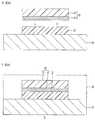
도 1은 본 발명의 형광 접착 시트의 일 실시형태의 단면도를 나타낸다.
도 2는 본 발명의 광반도체 장치의 일 실시형태인 LED 장치의 제조 방법의 공정도로서,
도 2(a)는 형광 접착 시트 및 LED를 각각 준비하는 공정,
도 2(b)는 형광 접착 시트를 LED에 감압 접착하는 공정을 나타낸다.
도 3은 본 발명의 광반도체 장치의 다른 실시형태인 LED 장치의 제조 방법의 공정도로서,
도 3(a)는 형광 접착 시트 및 LED를 각각 준비하는 공정,
도 3(b)는 형광 접착 시트를 LED에 감압 접착하는 공정을 나타낸다.
도 4는 본 발명의 광반도체 장치의 다른 실시형태인 LED 장치의 제조 방법의 공정도로서,
도 4(a)는 기판 및 LED-형광체층 감압 접착체를 각각 준비하는 공정,
도 4(b)는 LED-형광체층 감압 접착체의 LED를 기판에 실장하는 공정을 나타낸다.
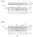
도 5는 본 발명의 광반도체 장치의 다른 실시형태의 제조 방법의 공정도로서,
도 5(a)는 LED 패키지, 및 형광 접착 시트를 준비하는 공정,
도 5(b)는 형광 접착 시트를 LED 패키지에 감압 접착하는 공정을 나타낸다.BRIEF DESCRIPTION OF THE DRAWINGS The cross section of one Embodiment of the fluorescent adhesive sheet of this invention is shown.
FIG. 2 is a process chart of a method of manufacturing an LED device that is an embodiment of the optical semiconductor device of the present invention.
2 (a) is a step of preparing a fluorescent adhesive sheet and LED, respectively,
2 (b) shows a process of pressure-sensitive bonding the fluorescent adhesive sheet to the LED.
3 is a process chart of a method of manufacturing an LED device which is another embodiment of the optical semiconductor device of the present invention.
3 (a) is a step of preparing a fluorescent adhesive sheet and LED, respectively;
3 (b) shows a process of pressure-sensitive bonding the fluorescent adhesive sheet to the LED.
4 is a process chart of a method of manufacturing an LED device which is another embodiment of the optical semiconductor device of the present invention.
4 (a) is a step of preparing a substrate and the LED-phosphor layer pressure-sensitive adhesive, respectively,
Fig. 4B shows a process of mounting the LED of the LED-phosphor layer pressure-sensitive adhesive on a substrate.
5 is a process chart of a manufacturing method of another embodiment of the optical semiconductor device of the present invention;
Figure 5 (a) is a step of preparing an LED package, and a fluorescent adhesive sheet,
Figure 5 (b) shows a process of pressure-sensitive bonding the fluorescent adhesive sheet to the LED package.
도 1에 있어서, 본 발명의 일 실시형태로서의 형광 접착 시트(6)는 형광체층(3), 및 형광체층(3)의 상면(두께 방향 한쪽 면)에 적층되는 접착제층(4)을 구비하고 있다.In FIG. 1, the fluorescent
형광체층(3)은, 예컨대 후술하는 LED(2)(도 2 참조)로부터 발광되는 청색광의 일부를 황색광으로 하는 파장 변환층(형광체층)이다. 또한, 형광체층(3)은, 상기한 파장 변환에 더하여, 청색광의 일부를 적색광으로 변환해도 좋다. 형광체층(3)은 플레이트상 또는 시트상으로 형성되어 있다. 형광체층(3)은, 예컨대 형광체의 세라믹으로부터 형광체 세라믹 플레이트로서 형성되거나, 또는 형광체 및 수지를 함유하는 형광체 수지 조성물로부터 형광체 수지 시트로서 형성되어 있다.The
형광체는 여기광으로서 파장 350∼480nm의 광의 일부 또는 전부를 흡수하여 여기되어, 여기광보다도 장파장, 예컨대 500∼650nm의 형광을 발광한다. 구체적으로는, 형광체로서는 예컨대 황색 형광체를 들 수 있다. 그와 같은 형광체로서는 예컨대 복합 금속 산화물이나 금속 황화물 등에 예컨대 세륨(Ce)이나 유로퓸(Eu) 등의 희토류 원소가 도핑된 형광체를 들 수 있다.The phosphor absorbs a part or all of the light having a wavelength of 350 to 480 nm as excitation light and is excited to emit fluorescence having a longer wavelength than the excitation light, for example, 500 to 650 nm. Specifically, a yellow phosphor is mentioned, for example. Such phosphors include, for example, composite metal oxides and metal sulfides, for example, phosphors doped with rare earth elements such as cerium (Ce) and europium (Eu).
구체적으로는, 형광체로서는 예컨대 Y3Al5O12:Ce(YAG(이트륨·알루미늄·가넷):Ce), (Y,Gd)3(Al,Ga)5O12:Ce, Tb3Al3O12:Ce, Lu3Al3O12:Ce, Ca3Sc2Si3O12:Ce, Lu2CaMg2(Si,Ge)3O12:Ce 등의 가넷형 결정 구조를 갖는 가넷형 형광체, 예컨대 (Sr,Ba)2SiO4:Eu, Ca3SiO4Cl2:Eu, Sr3SiO5:Eu, Li2SrSiO4:Eu, Ca3Si2O7:Eu 등의 실리케이트 형광체, 예컨대 CaAl12O19:Mn, SrAl2O4:Eu 등의 알루미네이트 형광체, 예컨대 ZnS:Cu,Al, CaS:Eu, CaGa2S4:Eu, SrGa2S4:Eu 등의 황화물 형광체, 예컨대 CaSi2O2N2:Eu, SrSi2O2N2:Eu, BaSi2O2N2:Eu, Ca-α-SiAlON 등의 산질화물 형광체, 예컨대 CaAlSiN3:Eu, CaSi5N8:Eu 등의 질화물 형광체, 예컨대 K2SiF6:Mn, K2TiF6:Mn 등의 불화물계 형광체 등을 들 수 있다. 바람직하게는 가넷형 형광체, 더 바람직하게는 Y3Al5O12:Ce(YAG)를 들 수 있다.Specifically, examples of the phosphor include Y3 Al5 O12 : Ce (YAG (yttrium aluminum garnet) Ce, Y, Gd3 Al, Ga5 O12 Ce, Tb3 Al3 O12 : Ce, Lu3 Al3 O12 : Ce, Ca3 Sc2 Si3 O12 : Ce, Lu2 CaMg2 (Si, Ge)3 O12 : Garnet-type phosphor having a garnet-type crystal structure, such as Ce, Silicate phosphors such as (Sr, Ba)2 SiO4 : Eu, Ca3 SiO4 Cl2 : Eu, Sr3 SiO5 : Eu, Li2 SrSiO4 : Eu, Ca3 Si2 O7 : Eu, for example CaAl12 O 19: Mn, SrAl 2 O 4: aluminate phosphors, such as Eu, for example, ZnS: Cu, Al, CaS: Eu, CaGa 2 S 4: Eu, SrGa 2 S 4: sulfide phosphor such as Eu, for example CaSi2 Oxynitride phosphors such as O2 N2 : Eu, SrSi2 O2 N2 : Eu, BaSi2 O2 N2 : Eu, Ca-α-SiAlON, such as CaAlSiN3 : Eu, CaSi5 N8 : Eu, etc. Nitride phosphors such as fluoride-based phosphors such as K2 SiF6 : Mn and K2 TiF6 : Mn. Preferably from garnet type fluorescent material, more preferably Y3 Al5 O12: there may be mentioned a Ce (YAG).
형광체는 단독 사용하거나 2종 이상 병용할 수 있다.Phosphor may be used alone or in combination of two or more.
형광체층(3)을 형광체 세라믹 플레이트로서 형성하기 위해서는, 상기한 형광체를 세라믹 재료로 하여, 이러한 세라믹 재료를 소결하는 것에 의해 형광체층(3)(형광체 세라믹)을 얻는다. 또는, 상기한 형광체의 원재료를 소결하여, 그에 의한 화학 반응에 의해 형광체층(3)(형광체 세라믹)을 얻을 수도 있다In order to form the
한편, 형광체 세라믹을 얻을 때에는, 소결 전에, 예컨대 바인더 수지, 분산제, 가소제, 소결 조제 등의 첨가제를 적절한 비율로 첨가할 수도 있다.On the other hand, when obtaining a fluorescent ceramic, additives, such as binder resin, a dispersing agent, a plasticizer, a sintering adjuvant, can also be added in an appropriate ratio before sintering.
한편, 형광체층(3)을 형광체 수지 조성물로 형성하기 위해서는, 예컨대, 우선, 상기한 형광체와 수지를 배합하는 것에 의해 형광체 수지 조성물을 조제한다.On the other hand, in order to form the
수지는 형광체를 분산시키는 매트릭스이고, 예컨대 실리콘 수지 조성물, 에폭시 수지, 아크릴 수지 등의 투명 수지 등을 들 수 있다. 바람직하게는, 내구성의 관점에서 실리콘 수지 조성물을 들 수 있다.Resin is a matrix which disperse | distributes fluorescent substance, For example, transparent resin, such as a silicone resin composition, an epoxy resin, an acrylic resin, etc. are mentioned. Preferably, silicone resin composition is mentioned from a viewpoint of durability.
실리콘 수지 조성물은, 주로 실록세인 결합(-Si-O-Si-)으로 이루어지는 주쇄, 및 주쇄의 규소 원자(Si)에 결합하는 알킬기(예컨대 메틸기 등), 아릴기(예컨대 페닐기 등) 또는 알콕실기(예컨대 메톡시기) 등의 유기기로 이루어지는 측쇄를 분자 내에 갖고 있다.The silicone resin composition is mainly composed of a siloxane bond (-Si-O-Si-), an alkyl group (such as a methyl group), an aryl group (such as a phenyl group) or an alkoxyl group bonded to a silicon atom (Si) of the main chain. The side chain which consists of organic groups, such as a methoxy group (for example), has in a molecule | numerator.
구체적으로는, 실리콘 수지 조성물로서는, 예컨대 탈수 축합 경화형 실리콘 레진, 부가 반응 경화형 실리콘 레진, 과산화물 경화형 실리콘 레진, 습기 경화형 실리콘 레진 등의 경화형 실리콘 레진 등을 들 수 있다.Specific examples of the silicone resin composition include curable silicone resins such as dehydration condensation-curable silicone resins, addition reaction curable silicone resins, peroxide curable silicone resins, and moisture-curable silicone resins.
실리콘 수지 조성물의 25℃에서의 동점도는 예컨대 10∼30mm2/s이다.The kinematic viscosity at 25 ° C. of the silicone resin composition is, for example, 10 to30 mm2 / s.
수지는 단독 사용하거나 2종 이상 병용할 수 있다.Resin can be used individually or in combination of 2 or more types.
각 성분의 배합 비율은, 형광체의 배합 비율이 형광체 수지 조성물에 대하여 예컨대 1질량% 이상, 바람직하게는 5질량% 이상이고, 또한 예컨대 50질량% 이하, 바람직하게는 30질량% 이하이기도 하다. 또한, 수지 100질량부에 대한 형광체의 배합 비율이 예컨대 1질량부 이상, 바람직하게는 5질량부 이상이고, 또한 예컨대 100질량부 이하, 바람직하게는 40질량부 이하이기도 하다.The mixing ratio of each component is, for example, 1% by mass or more, preferably 5% by mass or more, and, for example, 50% by mass or less, preferably 30% by mass or less, with respect to the phosphor resin composition. Moreover, the compounding ratio of fluorescent substance with respect to 100 mass parts of resin is 1 mass part or more, Preferably it is 5 mass parts or more, For example, 100 mass parts or less, Preferably it is 40 mass parts or less.
또한, 수지의 배합 비율은 형광체 수지 조성물에 대하여 예컨대 50질량% 이상, 바람직하게는 70질량% 이상이고, 예컨대 99질량% 이하, 바람직하게는 95질량% 이하이기도 하다.In addition, the compounding ratio of resin is 50 mass% or more with respect to fluorescent substance resin composition, Preferably it is 70 mass% or more, for example, 99 mass% or less, Preferably it is 95 mass% or less.
형광체 수지 조성물은 형광체 및 수지를 상기한 배합 비율로 배합하고, 교반 혼합하는 것에 의해 조제된다. 조제된 형광체 수지 조성물은 시트상으로 성형되어 있고, 구체적으로는 형광체 수지 시트로서 형성된다.The fluorescent substance resin composition is prepared by mix | blending fluorescent substance and resin in the said compounding ratio, and stirring and mixing. The prepared phosphor resin composition is molded into a sheet, and specifically, is formed as a phosphor resin sheet.
형광체 수지 시트는, 수지가 경화형 실리콘 레진을 함유하는 경우에는, B 스테이지 또는 C 스테이지로서 형성된다. 또한, 형광체 수지 시트는, B 스테이지로 형성되는 경우에는, 후의 가열에 의해 C 스테이지로 할 수도 있다.The fluorescent substance resin sheet is formed as B stage or C stage, when resin contains curable silicone resin. In addition, when it forms in a B stage, a fluorescent substance resin sheet can also be set as a C stage by subsequent heating.
형광체층(3)은, LED(2) 및 형광체층(3)에 의한 발열의 열 전도의 관점에서, 바람직하게는 형광체 세라믹 플레이트로부터 형성된다.The
형광체층(3)은, 형광체 세라믹 플레이트로서 형성되는 경우에는, 두께가 예컨대 50㎛ 이상, 바람직하게는 100㎛ 이상이고, 또한 예컨대 1000㎛ 이하, 바람직하게는 500㎛ 이하이다. 또한, 형광체 수지 시트로부터 형성되는 경우에는, 두께가 성막성 및 장치의 외관의 관점에서 예컨대 25㎛ 이상, 바람직하게는 50㎛ 이상이고, 또한 예컨대 1000㎛ 이하, 바람직하게는 200㎛ 이하이기도 하다.When the
접착제층(4)은 형광체층(3)의 상면(두께 방향 한쪽 면) 전체 면에 형성되어 있다. 접착제층(4)은 실리콘 감압 접착제 조성물로 시트상으로 형성되어 있다.The
실리콘 감압 접착제 조성물은, 예컨대 제 1 폴리실록세인, 제 2 폴리실록세인 및 촉매 등을 함유하는 원료로부터 조제된다.The silicone pressure sensitive adhesive composition is prepared, for example, from a raw material containing the first polysiloxane, the second polysiloxane, a catalyst, and the like.
제 1 폴리실록세인은 실리콘 감압 접착제 조성물의 주원료이고, 예컨대 실란올기 함유 폴리실록세인 등의 반응성 폴리실록세인을 들 수 있다.1st polysiloxane is a main raw material of a silicone pressure sensitive adhesive composition, For example, reactive polysiloxane, such as a silanol group containing polysiloxane, is mentioned.
실란올기 함유 폴리실록세인으로서는, 예컨대 실란올기 양말단 폴리실록세인을 들 수 있다.As a silanol group containing polysiloxane, a silanol group sock-end polysiloxane is mentioned, for example.
실란올기 양말단 폴리실록세인은 분자의 양말단에 실란올기(SiOH기)를 함유하는 오가노실록세인이고, 구체적으로는 하기 화학식 1로 표시된다.The silanol group sock-end polysiloxane is an organosiloxane containing a silanol group (SiOH group) in the sock end of a molecule | numerator, and is represented by following General formula (1).
(화학식 1 중, R1은 포화 탄화수소기 및 방향족 탄화수소기로부터 선택되는 1가 탄화수소기를 나타낸다. 또한, n은 1 이상의 정수를 나타낸다.)(In
상기 화학식 1 중, R1로 표시되는 1가 탄화수소기에 있어서 포화 탄화수소기로서는, 예컨대 탄소수 1∼6의 직쇄상 또는 분기상 알킬기(메틸기, 에틸기, 프로필기, 아이소프로필기, 뷰틸기, 아이소뷰틸기, 펜틸기, 헥실기 등), 예컨대 탄소수 3∼6의 사이클로알킬기(사이클로펜틸기, 사이클로헥실기 등) 등을 들 수 있다.As the saturated hydrocarbon group in the monovalent hydrocarbon group represented by R1 in
또한, 상기 화학식 1 중, R1로 표시되는 1가 탄화수소기에 있어서 방향족 탄화수소기로서는, 예컨대 탄소수 6∼10의 아릴기(페닐기, 나프틸기) 등을 들 수 있다.Moreover, as said aromatic hydrocarbon group in a monovalent hydrocarbon group represented by R <1> in the said General formula (1), a C6-C10 aryl group (phenyl group, naphthyl group) etc. are mentioned, for example.
상기 화학식 1에서, R1은 동일하거나 서로 달라도 좋고, 바람직하게는 동일하다.In
1가 탄화수소기로서는, 바람직하게는 탄소수 1∼6의 알킬기 및 탄소수 6∼10의 아릴기를 들 수 있고, 더 바람직하게는 메틸기, 페닐기를 들 수 있다.As monovalent hydrocarbon group, Preferably, a C1-C6 alkyl group and a C6-C10 aryl group are mentioned, More preferably, a methyl group and a phenyl group are mentioned.
상기 화학식 1에서, n은 바람직하게는 10,000 이하의 정수, 더 바람직하게는 1,000 이하의 정수이다.In
한편, 상기 화학식 1에서의 n은 평균값으로서 산출된다.On the other hand, n in the formula (1) is calculated as an average value.
실란올기 양말단 폴리실록세인으로서는, 구체적으로는 실란올기 양말단 폴리다이메틸실록세인, 실란올기 양말단 폴리메틸페닐실록세인, 실란올기 양말단 폴리다이페닐실록세인 등을 들 수 있다.Specific examples of the silanol-based sock-end polysiloxane include silanol-based sock-end polydimethyl siloxane, silanol-based sock-end polymethylphenyl siloxane, and silanol-based sock-end polydiphenyl siloxane.
이와 같은 제 1 폴리실록세인은 단독 사용하거나 상이한 복수 종류를 병용할 수 있다.Such 1st polysiloxane can be used individually or in combination of different types.
제 1 폴리실록세인 중에서는, 바람직하게는 실란올기 양말단 폴리다이메틸실록세인을 들 수 있다.In 1st polysiloxane, Preferably, a silanol-group sock end polydimethylsiloxane is mentioned.
제 1 폴리실록세인은 시판품을 이용할 수 있고, 또한 공지의 방법에 따라서 합성한 것을 이용할 수도 있다.A commercial item can be used for 1st polysiloxane, and what synthesize | combined according to a well-known method can also be used.
제 1 폴리실록세인의 수평균분자량은 예컨대 100 이상, 바람직하게는 200 이상이고, 또한 예컨대 1,000,000 이하, 바람직하게는 100,000 이하이기도 하다. 수평균분자량은 겔 침투 크로마토그래피에 의해 표준 폴리스타이렌으로 환산되어 산출된다.The number average molecular weight of the first polysiloxane is, for example, 100 or more, preferably 200 or more, and for example, 1,000,000 or less, preferably 100,000 or less. The number average molecular weight is calculated in terms of standard polystyrene by gel permeation chromatography.
제 1 폴리실록세인의 배합 비율은 실리콘 감압 접착제 조성물에 있어서 예컨대 60질량% 이상, 바람직하게는 80질량% 이상이고, 또한 예컨대 99.5질량% 이하, 바람직하게는 98질량% 이하이기도 하다.The blending ratio of the first polysiloxane is, for example, 60% by mass or more, preferably 80% by mass or more, and for example, 99.5% by mass or less, preferably 98% by mass or less in the silicone pressure-sensitive adhesive composition.
제 2 폴리실록세인은 실리콘 감압 접착제 조성물의 부원료이고, 예컨대 접착제층(4)의 경도의 향상, 접착력의 향상, 내열성의 향상과 같은 특성을 얻기 위해 필요에 따라 첨가된다. 제 2 폴리실록세인으로서는, 예컨대 쇄상 폴리실록세인, 환상 폴리실록세인 등을 들 수 있다. 바람직하게는, 환상 폴리실록세인을 들 수 있다.The second polysiloxane is a subsidiary material of the silicone pressure-sensitive adhesive composition, and is added as necessary in order to obtain properties such as improvement in hardness of the
환상 폴리실록세인은 하기 화학식 2로 표시된다.Cyclic polysiloxane is represented by following formula (2).

(화학식 2 중, R1은 화학식 1에서의 R1과 동일한 의미이다. m은 2 이상의 정수를 나타낸다.)(In the
m은 바람직하게는 3 이상의 정수를 나타내고, 또한 예컨대 10 이하의 정수, 바람직하게는 6 이하의 정수이기도 하다.m preferably represents an integer of 3 or more, and is also, for example, an integer of 10 or less, preferably an integer of 6 or less.
환상 폴리실록세인으로서는, 구체적으로는 헥사메틸사이클로트라이실록세인(화학식 2 중, R1이 메틸, m이 3), 옥타메틸사이클로테트라실록세인(화학식 2 중, R1이 메틸, m이 4), 데카메틸사이클로펜타실록세인(화학식 2 중, R1이 메틸, m이 5) 등을 들 수 있다.Specific examples of the cyclic polysiloxane include hexamethylcyclotrisiloxane (in
이와 같은 제 2 폴리실록세인은 단독 사용하거나 상이한 복수 종류를 병용할 수도 있다.Such a second polysiloxane may be used alone or in combination of a plurality of different kinds thereof.
제 2 폴리실록세인 중에서는, 바람직하게는 옥타메틸사이클로테트라실록세인을 들 수 있다.Among the second polysiloxanes, octamethylcyclotetrasiloxane is preferably used.
제 2 폴리실록세인의 배합 비율은 제 1 폴리실록세인 100질량부에 대하여 예컨대 20질량부 이하, 바람직하게는 10질량부 이하이다.The blending ratio of the second polysiloxane is, for example, 20 parts by mass or less, preferably 10 parts by mass or less with respect to 100 parts by mass of the first polysiloxane.
촉매로서는, 예컨대 과산화물을 들 수 있고, 그와 같은 과산화물로서는, 예컨대 다이벤조일 퍼옥사이드, 벤조일 m-메틸벤조일 퍼옥사이드, m-톨릴 퍼옥사이드 등의 벤조일계 과산화물 등의 유기 과산화물을 들 수 있다.Examples of the catalyst include peroxides, and examples of such peroxides include organic peroxides such as benzoyl peroxides such as dibenzoyl peroxide, benzoyl m-methylbenzoyl peroxide, and m-tolyl peroxide.
촉매는 단독 사용하거나 병용할 수 있다.The catalyst may be used alone or in combination.
촉매로서, 바람직하게는 다이벤조일 퍼옥사이드, 벤조일 m-메틸벤조일 퍼옥사이드 및 m-톨릴 퍼옥사이드의 병용(혼합물)을 들 수 있다.As a catalyst, Preferably, a combination (mixture) of dibenzoyl peroxide, benzoyl m-methylbenzoyl peroxide, and m-tolyl peroxide is mentioned.
촉매의 배합 비율은, 접착제층(4)의 경도를 제어하는 관점에서, 제 1 폴리실록세인 100질량부에 대하여 예컨대 0.5질량부 이상, 바람직하게는 1질량부 이상이고, 또한 10질량부 이하, 바람직하게는 5질량부 이하이기도 하다.From the viewpoint of controlling the hardness of the
그리고, 실리콘 감압 접착제 조성물은, 상기한 원료를 필요에 따라 용매에 배합하여 바니쉬를 조제하고, 계속해서 필요에 따라 그들을 반응시켜 조제된다. 용매로서는, 톨루엔 등의 방향족 탄화수소 등을 들 수 있다.And a silicone pressure-sensitive adhesive composition is mix | blended said raw material with a solvent as needed to prepare a varnish, and it is made to react by following them as needed, and to prepare it. As a solvent, aromatic hydrocarbons, such as toluene, etc. are mentioned.
한편, 상기한 용매는, 접착제층(4)의 피막을 형성한 후, 필요에 따라 증류 제거된다.In addition, after forming the film of the
상기한 실리콘 감압 접착제 조성물은 시판품을 이용할 수 있고, 예컨대 다우코닝사제의 280A, 282, 7355, 7358, 7502, 7657, Q2-7406, Q2-7566, Q2-7735, 예컨대 모멘티브사제의 PSA 590, PSA 600, PSA 595, PSA 610, PSA 518, PSA 6574, PSA 529, PSA 750-D1, PSA 825-D1, PSA 800-C 등이 이용된다.The silicone pressure-sensitive adhesive composition described above may use a commercially available product, for example, 280A, 282, 7355, 7358, 7502, 7657, Q2-7406, Q2-7566, Q2-7735 manufactured by Dow Corning, such as PSA 590 manufactured by Momentive, PSA 600, PSA 595, PSA 610, PSA 518, PSA 6574, PSA 529, PSA 750-D1, PSA 825-D1, PSA 800-C and the like are used.
이렇게 하여 형성되는 접착제층(4)의 두께는 감압 접착성의 관점에서 예컨대 5㎛ 이상이고, 또한 예컨대 200㎛ 이하, 바람직하게는 LED(2) 및 형광체층(3)에 의한 발열의 열 전도의 관점에서 100㎛ 이하, 보다 바람직하게는 50㎛ 이하이기도 하다.The thickness of the
다음으로, 이 형광 접착 시트(6)의 제조 방법에 대하여 설명한다.Next, the manufacturing method of this fluorescent
이 방법에서는, 우선, 형광체층(3)을 준비한다.In this method, first, the
이어서, 접착제층(4)을 형광체층(3)의 상면에 적층한다.Subsequently, the
구체적으로는, 실리콘 감압 접착제 조성물이 바니쉬로서 조제되는 경우에는, 바니쉬를 형광체층(3)의 상면 전체 면에, 예컨대 바 코터 등 공지의 도포 방법에 의해 도포한다. 이에 의해, 실리콘 감압 접착제 조성물의 피막을 형성한다. 계속해서, 필요에 따라 용매를 증류 제거한다.Specifically, when the silicone pressure sensitive adhesive composition is prepared as a varnish, the varnish is applied to the entire upper surface of the
또는, 바니쉬를 이형 시트 등의 표면에 도포하여 피막을 형성하고, 이러한 피막을, 필요에 따라 용매를 증류 제거한 후, 이형 시트로부터 형광체층(3)에 전사할 수도 있다. 이형 시트는 형광 접착 시트(6)의 사용 시에 접착제층(4)으로부터 떼어진다.Alternatively, the varnish may be applied to the surface of a release sheet or the like to form a coating. The coating may be transferred from the release sheet to the
이에 의해, 접착제층(4)을 형광체층(3)의 표면에 형성한다.Thus, the
이에 의해, 접착제층(4)이 형광체층(3)에 적층된 형광 접착 시트(6)를 얻는다.Thereby, the fluorescent
이렇게 하여 얻어지는 형광 접착 시트(6)에 있어서, 하기 박리 강도의 백분율은 30% 이상이고, 바람직하게는 35% 이상, 보다 바람직하게는 40% 이상이며, 또한 예컨대 200% 이하, 바람직하게는 150% 이하이기도 하다.In the thus obtained fluorescent
박리 강도의 백분율=[(75℃ 분위기에서의 박리 강도 PS75℃)/(25℃ 분위기에서의 박리 강도 PS25℃)]×100Percentage of Peel Strength = [(Peel Strength PS75 ° C. in 75 ° C. Atmosphere) / (Peel Strength PS25 ° C. in 25 ° C. Atmosphere)] × 100
75℃ 분위기에서의 박리 강도 PS75℃: 지지체에 적층된 접착제층(4)을 형광체층(3)에 감압 접착하고, 그 후, 온도 75℃에서 지지체 및 접착제층(4)을 박리 각도 180도, 속도 300mm/분으로 형광체층(3)으로부터 박리했을 때의 박리 강도. 즉, 75℃ 분위기에서의 접착제층(4)의 형광체층(3)에 대한 박리 강도.Peel strength in75 ° C. PS75 ° C . : Pressure sensitive adhesive bonding the
25℃ 분위기에서의 박리 강도 PS25℃: 지지체에 적층된 접착제층(4)을 형광체층(3)에 감압 접착하고, 그 후, 온도 25℃에서 지지체 및 접착제층(4)을 박리 각도 180도, 속도 300mm/분으로 형광체층(3)으로부터 박리했을 때의 박리 강도. 즉, 25℃ 분위기에서의 접착제층(4)의 형광체층(3)에 대한 박리 강도.Peel strength in25 ° C. PS25 ° C . : Pressure sensitive adhesive bonding the
박리 강도의 백분율이 30%에 못미치면, 접착제층(4)이 형광체층(3)으로부터 계면 박리된다는 문제가 있다.If the percentage of peel strength is less than 30%, there is a problem that the
한편, 접착제층(4)의 접착력이 상기 상한 이하이면, 감압 접착 대상인 LED(2)(도 2∼도 4 참조) 또는 LED 패키지(10)(도 5 참조)에 손상이 있는 경우에는, 형광 접착 시트(6)를 그들로부터 일단 떼어, 그들을 수리하는 리페어(repair)를 용이하게 실시할 수 있다.On the other hand, if the adhesive force of the
다음으로, 도 1의 형광 접착 시트(6)를 이용하여 본 발명의 광반도체 장치로서의 LED 장치(7)를 얻는 방법에 대하여, 도 2를 참조하여 설명한다.Next, a method of obtaining the LED device 7 as the optical semiconductor device of the present invention using the fluorescent
이 방법에서는, 도 2(a)의 상측도에 나타내는 바와 같이, 형광 접착 시트(6)를 준비한다.In this method, the fluorescent
형광 접착 시트(6)는 평면시에 있어서의 LED(2)의 외형 형상과 동일한 형상이 되도록 다이싱 등에 의해 외형 가공된다.The fluorescent
이와 함께, 도 2(a)의 하측도에 나타내는 바와 같이, 광반도체 소자로서의 LED(2)를 미리 기판(5)에 실장하여 준비한다.In addition, as shown in the lower side of FIG. 2A, the
LED(2)는 단면 대략 직사각 형상의 대략 평판 형상을 이루고, 공지의 반도체 재료로 형성되어 있다. 또한, LED(2)에는, 도시하지 않지만, 다음에 설명하는 기판(5)의 기판측 단자와 전기적으로 접속하기 위한 LED측 단자가 설치되어 있다.The
기판(5)은 평면시에 있어서 LED(2)보다 약간 큰 평판 형상으로 형성되어 있다. 기판(5)은, 예컨대 실리콘 기판, 세라믹 기판, 폴리이미드 수지 기판, 금속 기판에 절연층이 적층된 적층 기판 등의 절연 기판으로 이루어진다.The board |
또한, 기판(5)의 상면에는, LED(2)의 LED측 단자(도시하지 않음)와 전기적으로 접속하기 위한 기판측 단자(도시하지 않음), 및 그에 연속하는 배선을 구비하는 도체 패턴(도시하지 않음)이 형성되어 있다. 도체 패턴은 예컨대 금, 구리, 은, 니켈 등의 도체로 형성되어 있다.In addition, the upper surface of the board |
LED(2)는, 기판(5)에, 예컨대 플립 칩 실장 또는 와이어 본딩 접속에 의해 접속된다. 한편, LED(2)가 기판(5)에 와이어 본딩 접속되는 경우에는, LED(2)에 감압 접착하는 형광 접착 시트(6)는 와이어를 피하는(우회하는) 형상으로 형성된다.The
이어서, 이 방법에서는, 형광 접착 시트(6)를 LED(2)에 부착한다. 구체적으로는, 형광체층(3)을 접착제층(4)을 통해 LED(2)의 상면에 감압 접착한다. 즉, 접착제층(4)의 하면을 LED(2)의 상면에 접촉시킨다.Subsequently, in this method, the fluorescent
형광 접착 시트(6)와 LED(2)의 접합은 상온(구체적으로는 20∼25℃)에서 실시한다. 또는, 필요에 따라 형광 접착 시트(6)를 예컨대 30∼50℃로 가열하여 실시할 수도 있다.Bonding of the fluorescent
이에 의해, 기판(5), 기판(5)에 실장되는 LED(2), 및 LED(2)의 상면에 감압 접착하는 형광 접착 시트(6)를 구비하는 LED 장치(7)를 얻는다.Thereby, the LED device 7 provided with the board |
그 후, 필요에 따라, 도 2(b)의 가상선으로 나타내는 바와 같이, 제 1 봉지층(8)을 LED 장치(7)에 설치할 수도 있다. 제 1 봉지층(8)은, 기판(5)의 위에서 LED(2) 및 형광 접착 시트(6)를 피복하도록 투명 수지로 형성된다. 제 1 봉지층(8)은, LED 장치(7)에 설치된 후, 필요에 따라 예컨대 연마나 다이싱 등에 의해 사이즈가 조정된다.Then, as needed, as shown by the virtual line of FIG. 2 (b), the
그리고, 이 형광 접착 시트(6)에서는, 접착제층(4)이 실리콘 감압 접착제 조성물로 형성되고, 또한 상기한 형광 접착 시트(6)의 박리 강도의 백분율이 30% 이상이기 때문에, 내열성 및 내구성이 우수하다.And in this fluorescent
상세하게는, 형광 접착 시트(6)의 고온(예컨대 75℃를 포함하는 고온)의 접착력이 형광 접착 시트(6)의 상온(25℃)의 접착력에 비해 현저히 저하되는 것을 방지할 수 있기 때문에, 우수한 내열성을 확보할 수 있다.In detail, since the adhesive force of the high temperature (for example, high temperature containing 75 degreeC) of the fluorescent
또한, 접착제층(4)이 실리콘 감압 접착제 조성물로 형성되기 때문에, 접착제층(4)의 열화를 유효하게 억제하여, LED 장치(7)에 있어서 휘도의 저하를 억제할 수 있다.Moreover, since the
그 결과, LED 장치(7)는 상기한 형광 접착 시트(6)를 구비하기 때문에, 장기에 걸쳐 우수한 발광 신뢰성을 확보할 수 있다.As a result, since the LED device 7 is equipped with the above-mentioned fluorescent
도 3 이후의 각 도면에 있어서, 상기한 각 부에 대응하는 부재 및 공정에 대해서는 동일한 참조 부호를 붙이고, 그의 상세한 설명을 생략한다.In each figure after FIG. 3, the same code | symbol is attached | subjected about the member and process corresponding to each said part, and the detailed description is abbreviate | omitted.
도 2(b)의 실시형태에 있어서의 LED 장치(7)에서는, 형광 접착 시트(6)를 LED(2)의 상면에만 감압 접착시키고 있지만, 예컨대 도 3(b)에 나타내는 바와 같이, LED(2)의 상면 및 측면에 감압 접착시킬 수도 있다.In the LED device 7 in the embodiment of FIG. 2B, the fluorescent
도 3(b)에 나타내는 LED 장치(7)를 얻기 위해서는, 도 1이 참조되는 바와 같이, 우선, 접착제층(4)을 형광체층(3)의 상면 전체 면에 적층하고, 그 후, 필요에 따라 그들을 LED(2)보다 큰 사이즈로 외형 가공하여, LED(2)보다 큰 사이즈의 형광 접착 시트(6)를 얻는다.In order to obtain the LED device 7 shown in FIG. 3 (b), as shown in FIG. 1, first, the
이어서, 형광 접착 시트(6)를, 기판(5)에 미리 실장된 LED(2)의 상면 및 측면에 부착한다.Next, the fluorescent
이 LED 장치(7)에서는, 도 3(b)에 나타내는 바와 같이, LED(2)의 상면 및 측면에는 접착제층(4)이 연속하여 적층되어 있다.In this LED device 7, as shown in FIG.3 (b), the
또한, 접착제층(4)의 표면(상면 및 측면)에는 형광체층(3)이 적층되어 있다.In addition, the
형광체층(3) 및 접착제층(4)은, 하방으로 개방되는 단면 대략 ㄷ자 형상으로 형성되어 있다.The
이에 의해, 형광체층(3)은, 접착제층(4)을 통해 LED(2)의 상면 및 측면의 양면에 대해 감압 접착된다.Thereby, the
도 3의 실시형태에 의해서도 도 2와 마찬가지의 작용효과를 나타낸다.According to the embodiment of FIG. 3, the same effects as in FIG. 2 are obtained.
또한, 도 2의 실시형태에서는, 도 2(a)에 나타내는 바와 같이, 형광 접착 시트(6)를 준비하고, 별도로 LED(2)를 미리 기판(5)에 실장하여 준비해 두고, 그 후, 도 2(b)에 나타내는 바와 같이, 형광 접착 시트(6)를 기판(5)의 위에서 LED(2)에 감압 접착하는 것에 의해 LED 장치(7)를 제작하고 있다.In addition, in embodiment of FIG. 2, as shown to FIG. 2 (a), the fluorescent
그러나, 예컨대, 우선, 도 4(a)에 나타내는 바와 같이, 형광 접착 시트(6)와 LED(2)를 감압 접착하여, 그들로 이루어지는 광반도체 소자-형광체층 감압 접착체로서의 LED-형광체층 감압 접착체(1)를 기판(5)과는 별도로 제작하고, 그 후, 도 4(b)에 나타내는 바와 같이, LED-형광체층 감압 접착체(1)의 LED(2)를 기판(5)에 실장할 수도 있다.However, for example, first, as shown in Fig. 4A, the fluorescent
이 방법에서는, 우선, 형광 접착 시트(6)와 LED(2)를 준비하고, 그들을 접합한다. 구체적으로는, 형광체층(3)을 접착제층(4)을 통해 LED(2)의 상면에 감압 접착시킨다.In this method, first, the fluorescent
이에 의해, LED(2)와, LED(2)의 상면(두께 방향 한쪽 면)에 감압 접착하는 형광 접착 시트(6)를 구비하는 LED-형광체층 감압 접착체(1)를 제작한다.Thereby, the LED-phosphor layer pressure-sensitive-adhesive 1 is provided which includes the
이어서, 도 4(b)에 나타내는 바와 같이, LED-형광체층 감압 접착체(1)의 LED(2)를 기판(5)에 실장한다.Subsequently, as shown in Fig. 4B, the
이에 의해, LED 장치(7)를 얻는다.Thereby, the LED device 7 is obtained.
도 4의 실시형태에 의해서도 도 2의 실시형태와 마찬가지의 작용효과를 나타낸다. 또한, LED-형광체층 감압 접착체(1)는 형광 접착 시트(6)를 구비하기 때문에, 내열성 및 내구성이 우수하다.4 shows the same effects as the embodiment of FIG. 2. Moreover, since the LED-phosphor layer pressure
또한, 도 2 및 도 3의 실시형태에서는, 형광 접착 시트(6)를 LED(2)에 부착하고 있지만, 예컨대 도 5에 나타내는 바와 같이, LED 패키지(10)에 부착할 수도 있다.In addition, although the fluorescent
도 5(a)에 있어서, LED 패키지(10)는, 기판(5), 기판(5)에 실장되는 LED(2), 기판(5)의 위에 형성되고, 두께 방향으로 투영했을 때에 LED(2)를 둘러싸도록 배치되는 리플렉터(11), 및 리플렉터(11) 내에 충전되고, LED(2)를 봉지하는 봉지층으로서의 제 2 봉지층(12)을 구비한다.In FIG. 5A, the
LED(2)는 미리 기판(5)에 실장되어 있다.The
리플렉터(11)는, 평면시에 있어서 중앙이 개구되는 대략 직사각형 프레임 형상 또는 대략 링 형상(원환(圓環) 형상 또는 타원환 형상)으로 형성되어 있다. 또한, 리플렉터(11)는, 단면시에 있어서 상방을 향해 점차 폭이 좁아지는 대략 사다리꼴 형상으로 형성되어 있다. 리플렉터(11)는 LED(2)를 둘러싸도록 LED(2)와 간격을 두고 배치되어 있다. 즉, LED(2)는 리플렉터(11) 내에 배치되어 있다.The
리플렉터(11)는, 예컨대 광반사 성분(예컨대 산화타이타늄 등)을 함유하는 세라믹 재료의 소결체나, 광반사 성분을 함유하는 반사 수지 조성물 등으로 형성되어 있고, LED(2)로부터 발광되는 광을 반사한다.The
제 2 봉지층(12)은 리플렉터(11) 내에 충전되어 있고, 구체적으로는 리플렉터(11)의 내측면과, LED(2)로부터 노출되는 기판(5)의 상면과, LED(2)의 상면 및 외측면을 피복하도록 형성되어 있다.The
또한, 제 2 봉지층(12)의 상면은, 리플렉터(11)의 상면과, 면 방향(두께 방향에 직교하는 방향)을 따르는 동일 평면을 형성하도록 형성되어 있다. 한편, 도시하지 않지만, 제 2 봉지층(12)의 상면에, 둘레 단부(端部)로부터 중앙부를 향해 점차 하방으로 우묵하게 들어간 오목부(도시하지 않음)가 형성되어 있어도 좋다.Moreover, the upper surface of the
형광 접착 시트(6)를 LED 패키지(10)에 부착하기 위해서는, 도 5(a)에 나타내는 바와 같이, 형광 접착 시트(6) 및 LED 패키지(10)를 각각 준비한다.In order to attach the fluorescent
이어서, 도 5(b)에 나타내는 바와 같이, 형광 접착 시트(6)를 LED 패키지(10)의 상면에, 예컨대 상온(구체적으로는 20∼25℃)에서 부착한다.Next, as shown in FIG. 5B, the fluorescent
이에 의해, 상면(두께 방향 한쪽 면)에 형광체층(3)이 접착제층(4)을 통해 감압 접착된 LED 패키지(10)를 구비하는 LED 장치(7)를 제조할 수 있다.Thereby, the LED device 7 provided with the
도 5의 실시형태에 의해서도 도 2의 실시형태와 마찬가지의 작용효과를 나타낼 수 있다.Also in the embodiment of FIG. 5, the same effects as in the embodiment of FIG. 2 can be obtained.
또한, 도 2∼도 5의 실시형태에서는, 본 발명의 광반도체 소자로서 LED(2)를 들어 설명하고 있지만, 예컨대 LD(레이저 다이오드)(2)를 채용할 수도 있다.In addition, although the
그 경우에는, LED 장치(7)는 레이저 다이오드 조사 장치(7)로 여겨지고, 또한 LED-형광체층 감압 접착체(1)는 LD-형광체층 감압 접착체(1)로 여겨지며, LED 패키지(10)는 LD 패키지(10)로 여겨진다.In that case, the LED device 7 is regarded as a laser diode irradiation device 7, and the LED-phosphor layer pressure-
실시예Example
이하에, 제작예, 준비예, 비교 준비예, 실시예 및 비교예를 들어 본 발명을 더 상세히 설명하지만, 본 발명은 하등 그들에 한정되지 않는다.Although a production example, a preparation example, a comparative preparation example, an Example, and a comparative example are given to the following and this invention is demonstrated in detail, this invention is not limited to them at all.
(형광체 세라믹 플레이트의 제작)(Production of phosphor ceramic plate)
제작예 1Production Example 1
산화이트륨 입자(순도 99.99%, lot: N-YT4CP, 닛폰이트륨사제) 11.34g, 산화알루미늄 입자(순도 99.99%, 제품명 「AKP-30」, 스미토모화학사제) 8.577g, 및 산화세륨 입자 0.087g으로 이루어지는 형광체의 원료 분말을 조제했다.With yttrium oxide particles (purity 99.99%, lot: N-YT4CP, manufactured by Nippon Yttrium) 11.34 g, aluminum oxide particles (purity 99.99%, product name `` AKP-30 '', Sumitomo Chemical Corporation) 8.577 g, and cerium oxide particles 0.087 g The raw material powder of the fluorescent substance formed was prepared.
조제한 형광체의 원료 분말 20g과, 수용성 바인더 수지(「WB4101」, Polymer Inovations, Inc사제)를, 고형분의 체적 비율이 60:40으로 되도록 혼합하고, 추가로 증류수를 가하여 알루미나제 용기에 넣고, 직경 3mm의 이트륨 안정화 지르코니아 볼을 가하여 24시간 동안 볼 밀에 의해 습식 혼합함으로써, 형광체의 원료 입자의 슬러리 용액을 조제했다.20 g of the raw material powder of the prepared phosphor and a water-soluble binder resin ("WB4101", manufactured by Polymer Inovations, Inc.) are mixed so that the volume ratio of solid content is 60:40, and distilled water is added to the alumina container, and the diameter is 3 mm. A yttrium stabilized zirconia ball was added and wet mixed with a ball mill for 24 hours to prepare a slurry solution of raw material particles of the phosphor.
이어서, 조제한 슬러리 용액을 닥터 블레이드법에 의해 PET 필름 상에 테이프 캐스팅하고, 70℃에서 건조하여 세라믹 그린 시트를 형성한 후, 세라믹 그린 시트를 PET 필름으로부터 박리하여 두께 90㎛의 세라믹 그린 시트를 얻었다.Subsequently, the prepared slurry solution was tape cast on a PET film by a doctor blade method, dried at 70 ° C to form a ceramic green sheet, and then the ceramic green sheet was peeled from the PET film to obtain a ceramic green sheet having a thickness of 90 µm. .
그 후, 얻어진 그린 시트를 20mm×20mm의 사이즈로 잘라내고, 이를 2장 제작하여, 그들을 중첩시키고, 2축 핫 프레스를 이용하여 열 라미네이트하는 것에 의해 세라믹 그린 시트 적층체를 제작했다.Then, the obtained green sheet was cut out to the size of 20 mm x 20 mm, two sheets were produced, they were piled up, and the ceramic green sheet laminated body was produced by thermal lamination using the biaxial hot press.
그 후, 제작한 세라믹 그린 시트 적층체를 전기 머플 노에서 대기 중 1℃/분의 승온 속도로 1200℃까지 가열하여 바인더 수지 등의 유기 성분을 분해 제거하는 탈바인더 처리를 실시했다. 그 후, 고온 진공 노에 적층체를 옮겨, 약 10-3Torr(133×10-3N/m2)의 감압 하에서 5℃/분의 승온 속도로 1750℃까지 가열하고, 그 온도에서 5시간 소성함으로써 두께 150㎛의 형광체 세라믹 플레이트(형광체 시트)를 제작했다.Thereafter, the produced ceramic green sheet laminate was heated in an electric muffle furnace to 1200 ° C. at an elevated temperature rate of 1 ° C./min in the air, and debinding treatment was performed to decompose and remove organic components such as binder resin. Thereafter, the laminate was transferred to a high temperature vacuum furnace, and heated to 1750 ° C. at a temperature increase rate of 5 ° C./min under a reduced pressure of about 10−3 Torr (133 × 10−3 N / m2 ), and at that temperature for 5 hours. By baking, a fluorescent ceramic plate (phosphor sheet) having a thickness of 150 µm was produced.
(형광체 수지 시트의 제작)(Production of phosphor resin sheet)
제작예 2Production Example 2
YAG 형광체 분말(제품명 BYW01A, 평균 입자 직경 9㎛, Phosphor Tech사제)를 2액 혼합 타입의 열경화성 실리콘 엘라스토머(신에쓰실리콘사제, 제품명 KER2500)에, YAG 형광체 분말의 농도가 25질량%로 되도록 분산시킨 용액을, 애플리케이터를 이용하여 유리판 상에 도공하여 두께 150㎛의 형광체 피막을 형성하고, 형광체 피막을 100℃에서 1시간, 계속해서 150℃에서 1시간 가열하는 것에 의해 두께 150㎛의 C 스테이지의 형광체 수지 시트(형광체 시트)를 제작했다.YAG phosphor powder (product name BYW01A, average particle diameter of 9 μm, manufactured by Phosphor Tech) was dispersed in a two-liquid mixed type thermosetting silicone elastomer (Shin-Etsu Silicone Co., Ltd. product name KER2500) so that the concentration of the YAG phosphor powder was 25% by mass. The solution was coated on a glass plate using an applicator to form a phosphor film having a thickness of 150 μm, and the phosphor film was heated at 100 ° C. for 1 hour and then at 150 ° C. for 1 hour to form a phosphor having a C stage of 150 μm in thickness. A resin sheet (phosphor sheet) was produced.
(실리콘 감압 접착제 조성물의 준비)(Preparation of silicone pressure sensitive adhesive composition)
준비예 1Preparation Example 1
실리콘 감압 접착제 조성물(상품명 PSA 600, 모멘티브사제)을 준비했다.Silicone pressure-sensitive adhesive composition (trade name PSA 600, manufactured by Momentive) was prepared.
한편, 실리콘 감압 접착제 조성물의 원료는 이하와 같았다.In addition, the raw material of a silicone pressure sensitive adhesive composition was as follows.
·실란올기 양말단 폴리다이메틸실록세인Silanol group sock-stage polydimethylsiloxane
·옥타메틸사이클로테트라실록세인(화학식 2 중, R1: 모두 메틸, m: 3): 1∼5질량%(고형분 총량에 대하여)Octmethylcyclotetrasiloxane (in
·벤조일계 과산화물의 혼합물(다이벤조일 퍼옥사이드, 벤조일 m-메틸벤조일 퍼옥사이드 및 m-톨릴 퍼옥사이드의 혼합물): 소량Mixture of benzoyl peroxides (mixture of dibenzoyl peroxide, benzoyl m-methylbenzoyl peroxide and m-tolyl peroxide): small amount
·톨루엔: 고형분에 대하여 45질량%Toluene: 45 mass% with respect to solid content
(실리콘 감압 접착제 조성물의 준비)(Preparation of silicone pressure sensitive adhesive composition)
비교 준비예 1Comparative Preparation Example 1
실리콘 감압 접착제 조성물(상품명 SD 4580 PSA, 도레이 다우코닝사제)을 준비했다.A silicone pressure sensitive adhesive composition (trade name SD 4580 PSA, manufactured by Toray Dow Corning Corporation) was prepared.
한편, 실리콘 감압 접착제 조성물의 원료는 이하와 같았다.In addition, the raw material of a silicone pressure sensitive adhesive composition was as follows.
·실란올기 양말단 폴리다이메틸실록세인Silanol group sock-stage polydimethylsiloxane
·벤조일계 과산화물의 혼합물(다이벤조일 퍼옥사이드, 벤조일 m-메틸벤조일 퍼옥사이드 및 m-톨릴 퍼옥사이드의 혼합물): 소량Mixture of benzoyl peroxides (mixture of dibenzoyl peroxide, benzoyl m-methylbenzoyl peroxide and m-tolyl peroxide): small amount
·톨루엔: 고형분에 대하여 70질량%Toluene: 70 mass% with respect to solid content
(아크릴 감압 접착제 조성물의 준비)(Preparation of acrylic pressure sensitive adhesive composition)
비교 준비예 2Comparative Preparation Example 2
일본 특허공개 평6-172729호 공보의 실시예 2의 처방을 참고로 하여 아크릴 감압 접착제를 준비했다.The acrylic pressure sensitive adhesive was prepared with reference to the prescription of Example 2 of Unexamined-Japanese-Patent No. 6-172729.
(형광 접착 시트 및 LED 장치의 제조)(Manufacture of Fluorescent Adhesive Sheet and LED Device)
실시예 1Example 1
제작예 1의 형광체 세라믹 플레이트의 상면 전체 면에 준비예 1의 실리콘 감압 접착제 조성물을 도포하여 피막을 형성했다. 계속해서, 용매를 증류 제거했다.The silicone pressure-sensitive adhesive composition of Preparation Example 1 was applied to the entire upper surface of the phosphor ceramic plate of Production Example 1 to form a film. Subsequently, the solvent was distilled off.
이에 의해, 두께 40㎛의 실리콘 감압 접착제층(접착제층)을 형성했다(도 1 참조).This formed the silicon pressure sensitive adhesive layer (adhesive layer) of 40 micrometers in thickness (refer FIG. 1).
그 후, 형광체 세라믹 플레이트 및 실리콘 감압 접착제층을 합쳐서 다이싱함으로써, 사이즈 1mm×1mm의 형광 접착 시트를 제작했다(도 2(a)의 상측도 참조).Thereafter, the phosphor ceramic plate and the silicon pressure-sensitive adhesive layer were combined and diced to produce a fluorescent adhesive sheet having a size of 1 mm x 1 mm (see the upper side of Fig. 2 (a)).
그 후, 형광 접착 시트를, 미리 기판에 실장되고 형광 접착 시트와 동일한 사이즈의 LED(Cree제)(도 2(a) 참조)에 25℃에서 접합했다(도 2(b) 참조). 즉, 형광체 세라믹 플레이트를, 실리콘 감압 접착제층을 통해 LED에 감압 접착했다.Thereafter, the fluorescent adhesive sheet was previously mounted on a substrate and bonded to an LED (manufactured by Cree) (see Fig. 2 (a)) having the same size as the fluorescent adhesive sheet at 25 ° C (see Fig. 2 (b)). That is, the fluorescent ceramic plate was pressure-sensitively bonded to LED through the silicone pressure sensitive adhesive layer.
이에 의해, LED 장치를 제조했다.This manufactured the LED device.
실시예 2Example 2
제작예 1의 형광체 세라믹 플레이트 대신에 제작예 2의 형광체 수지 시트를 이용한 것 이외는, 실시예 1과 마찬가지로 처리하여 형광 접착 시트를 얻고(도 1 참조), 계속해서 LED 장치를 제조했다(도 2(b) 참조).A fluorescent adhesive sheet was obtained in the same manner as in Example 1 except that the phosphor resin sheet of Preparation Example 2 was used instead of the phosphor ceramic plate of Production Example 1 (see FIG. 1), and then an LED device was manufactured (FIG. 2). (b)).
실시예 3Example 3
실리콘 감압 접착제층의 두께를 60㎛로 변경한 것 이외는, 실시예 1과 마찬가지로 처리하여 형광 접착 시트를 얻고(도 1 참조), 계속해서 LED 장치를 제조했다(도 2(b) 참조).Except having changed the thickness of the silicone pressure sensitive adhesive layer into 60 micrometers, it processed similarly to Example 1, the fluorescent adhesive sheet was obtained (refer FIG. 1), and the LED device was manufactured continuously (refer FIG. 2 (b)).
실시예 4Example 4
실리콘 감압 접착제층의 두께를 120㎛로 변경한 것 이외는, 실시예 1과 마찬가지로 처리하여 형광 접착 시트를 얻고(도 1 참조), 계속해서 LED 장치를 제조했다(도 2(b) 참조).Except having changed the thickness of the silicone pressure sensitive adhesive layer into 120 micrometers, it processed similarly to Example 1, the fluorescent adhesive sheet was obtained (refer FIG. 1), and the LED device was manufactured continuously (refer FIG. 2 (b)).
비교예 1Comparative Example 1
준비예 1의 실리콘 감압 접착제 조성물 대신에 비교 준비예 1의 실리콘 감압 접착제 조성물을 이용한 것 이외는, 실시예 1과 마찬가지로 처리하여 형광 접착 시트를 얻고(도 1 참조), 계속해서 LED 장치를 제조했다(도 2(b) 참조).The same procedure as in Example 1 was repeated except that the silicone pressure sensitive adhesive composition of Comparative Preparation Example 1 was used instead of the silicone pressure sensitive adhesive composition of Preparation Example 1 to obtain a fluorescent adhesive sheet (see FIG. 1), and subsequently an LED device was manufactured. (See Figure 2 (b)).
비교예 2Comparative Example 2
준비예 1의 실리콘 감압 접착제 조성물 대신에 비교 준비예 2의 아크릴 감압 접착제 조성물을 이용한 것 이외는, 실시예 1과 마찬가지로 처리하여 형광 접착 시트를 얻고(도 1 참조), 계속해서 LED 장치를 제조했다(도 2(b) 참조).Except for using the acrylic pressure-sensitive adhesive composition of Comparative Preparation Example 2 in place of the silicone pressure-sensitive adhesive composition of Preparation Example 1, the same procedure as in Example 1 was carried out to obtain a fluorescent adhesive sheet (see Fig. 1), and subsequently an LED device was manufactured. (See Figure 2 (b)).
비교예 3Comparative Example 3
준비예 1의 실리콘 감압 접착제 조성물 대신에 비교 준비예 2의 아크릴 감압 접착제 조성물을 이용한 것 이외는, 실시예 2와 마찬가지로 처리하여 형광 접착 시트를 얻고(도 1 참조), 계속해서 LED 장치를 제조했다(도 2(b) 참조).Except for using the acrylic pressure-sensitive adhesive composition of Comparative Preparation Example 2 in place of the silicone pressure-sensitive adhesive composition of Preparation Example 1, the same procedure as in Example 2 was carried out to obtain a fluorescent adhesive sheet (see Fig. 1), and subsequently an LED device was manufactured. (See Figure 2 (b)).
각 실시예 및 각 비교예에 있어서의 형광체층 및 접착제층에 이용된 재료 등을 표 1에 나타낸다.Table 1 shows the materials used for the phosphor layer and the adhesive layer in each example and each comparative example.

(평가)(evaluation)
실시예 및 비교예의 각각의 감압 접착제층에 대하여, 형광체 시트에 대한 박리 강도를 이하의 방법에 의해 평가했다.About each pressure-sensitive adhesive layer of an Example and a comparative example, the peeling strength with respect to a fluorescent substance sheet was evaluated by the following method.
또한, 실시예 및 비교예의 각각의 LED 장치를 점등했을 때의 형광 접착 시트의 표면 온도, 및 경시적인 발광 신뢰성도 평가했다. 그들의 결과를 표 2에 나타낸다.Moreover, the surface temperature of the fluorescent adhesive sheet at the time of lighting each LED apparatus of an Example and a comparative example and light emission reliability over time were also evaluated. The results are shown in Table 2.
1. 박리 강도1. Peel strength
25℃와 75℃의 각각의 분위기에서의 감압 접착제층의 형광체 세라믹 플레이트에 대한 박리 강도를, 19mm 폭에서의 박리 접착력 측정[N/19mm]에 의해 산출했다.The peeling strength with respect to the fluorescent substance ceramic plate of the pressure-sensitive-adhesive layer in each atmosphere of 25 degreeC and 75 degreeC was computed by the peeling adhesive force measurement [N / 19mm] in 19 mm width.
상세하게는, 지지체로서의 두께 25㎛의 폴리이미드 필름의 표면에 감압 접착제 조성물을 폭이 19mm로 되고 또한 두께가 40㎛로 되도록 도공했다. 이에 의해, 지지체에 적층된 감압 접착제층을 형성했다. 이어서, 사이즈 20mm×20mm의 형광체 세라믹 플레이트에, 감압 접착제층 부착 폴리이미드 필름을 폴리이미드 필름의 위로부터 2kg의 롤러로 1 왕복하는 것에 의해 압착했다. 압착 후, 약 30분 방치했다. 그 후, 소정 온도로 설정된 항온조 내에 구비된 인장 시험 장치 내(장치명: 시마즈제작소사제, 항온조 내의 인장 시험기 AUTOGRAPH AG-10kNX)에 세팅하여 하기 온도 분위기에서 5분간 유지하고, 그 후, 폴리이미드 필름을 감압 접착제층과 함께 형광체 세라믹 플레이트로부터 하기 조건에서 떼어(박리하여), 그때의 박리 접착력을 박리 강도로서 측정했다.Specifically, the pressure-sensitive adhesive composition was coated on the surface of a polyimide film having a thickness of 25 μm as a support such that the width became 19 mm and the thickness became 40 μm. This formed the pressure sensitive adhesive layer laminated | stacked on the support body. Next, the polyimide film with a pressure sensitive adhesive layer was crimped | bonded to the fluorescent substance ceramic plate of size 20mmx20mm by one reciprocating with a roller of 2 kg from the top of a polyimide film. It left for about 30 minutes after crimping | bonding. Then, it set in the tension test apparatus (apparatus name: Shimadzu Corporation make, the tension tester AUTOGRAPH AG-10kNX in a thermostat set) provided in the thermostat set to predetermined temperature, hold | maintained for 5 minutes in the following temperature atmosphere, and the polyimide film after that It peeled off from the fluorescent ceramic plate with the pressure sensitive adhesive layer on the following conditions, and peeled off, and the peeling adhesive force at that time was measured as peeling strength.
항온조 내의 온도: 25℃ 또는 75℃Temperature in thermostat: 25 ℃ or 75 ℃
박리(떼기) 조건: 박리 각도 180도Peeling condition: 180 degree peeling angle
인장 속도 300mm/분 Tensile Speed 300mm / min
측정 후, 75℃ 분위기에서의 박리 강도 PS75℃[N/19mm]의 25℃ 분위기에서의 박리 강도 PS25℃[N/19mm]에 대한 백분율([PS75℃/PS25℃]×100)을 산출했다.After measurement, the percentage of peel strength PS75° C. [N / 19 mm] in75° C. atmosphere to peel strength PS25° C. [N / 19 mm] in 25 ° C. atmosphere ([PS75° C./PS25° C. ] × 100) Calculated.
2. LED 장치를 점등했을 때의 형광체층의 표면 온도2. Surface temperature of phosphor layer when lighting LED device
실시예 및 비교예의 각각의 LED 장치를 충분한 사이즈의 히트 싱크(heat sink)와 열 전도 그리스에 의해 접속시키고, 또한 전원과 전기적으로 접속했다. 이어서, 전원으로부터 350mA의 전류를 인가하여 LED 장치를 발광시키고, 1분간 발광시킨 후의 형광체층의 표면 온도를 서모그래피로 측정했다.Each LED device of the Example and the comparative example was connected with a heat sink of sufficient size and heat conductive grease, and also electrically connected with the power supply. Subsequently, a 350 mA electric current was applied from a power supply, the LED device was made to emit light, and the surface temperature of the phosphor layer after making it emit light for 1 minute was measured by thermography.
한편, 비교예 1에 대해서는, 접착제층이 형광체 세라믹 플레이트로부터 박리되었다. 그 때문에, 형광체층의 표면 온도를 측정할 수 없었다.On the other hand, for Comparative Example 1, the adhesive layer was peeled off from the phosphor ceramic plate. Therefore, the surface temperature of the phosphor layer could not be measured.
3. 경시적인 발광 신뢰성3. Light emission reliability over time
상기 2.에서 제작한 LED 장치를 350mA에서 초기 발광시켰을 때의 발광 휘도(초기 휘도)와, 30일간 연속하여 발광시켰을 때의 휘도(30일 후 휘도)를 각각 측정했다.The light emission luminance (initial luminance) when the LED device produced in the
그리고, 30일 후 휘도의 초기 휘도에 대한 백분율([30일 후 휘도/초기 휘도]×100)을 산출했다.The percentage ([luminance after 30 days / initial luminance] × 100) of the initial luminance of the luminance after 30 days was calculated.
한편, 비교예 1에 대해서는, 접착제층이 형광체 세라믹 플레이트로부터 박리되었기 때문에 30일 후 휘도를 측정할 수 없어, 상기한 백분율을 산출할 수 없었다.On the other hand, in Comparative Example 1, since the adhesive layer was peeled off from the phosphor ceramic plate, luminance could not be measured after 30 days, and the above percentage could not be calculated.

한편, 상기 설명은 본 발명의 예시의 실시형태로서 제공했지만, 이는 단순한 예시에 불과하며, 한정적으로 해석해서는 안된다. 당해 기술분야의 당업자에 의해 분명한 본 발명의 변형예는 후기의 특허청구의 범위에 포함되는 것이다.On the other hand, the above description is provided as an example of the present invention, but this is merely an example, and should not be construed as limiting. Variations of the invention which will be apparent to those skilled in the art are included in the following claims.
1: LED-형광체 감압 접착체2: LED
3: 형광체층4: 접착제층
5: 기판6: 형광 접착 시트
7: LED 장치8: 제 1 봉지층
10: LED 패키지11: 리플렉터
12: 제 2 봉지층1: LED-phosphor pressure sensitive adhesive 2: LED
3: phosphor layer 4: adhesive layer
5: substrate 6: fluorescent adhesive sheet
7: LED device 8: first encapsulation layer
10: LED Package 11: Reflector
12: second encapsulation layer
Claims (7)
Translated fromKorean상기 형광체층의 두께 방향 한쪽 면에 적층되는 접착제층을 구비하며,
상기 접착제층은 실리콘 감압 접착제 조성물로 형성되고,
하기 박리 강도의 백분율이 30% 이상인 것을 특징으로 하는 형광 접착 시트.
박리 강도의 백분율=[(75℃ 분위기에서의 박리 강도 PS75℃)/(25℃ 분위기에서의 박리 강도 PS25℃)]×100
75℃ 분위기에서의 박리 강도 PS75℃: 지지체에 적층된 상기 접착제층을 상기 형광체층에 감압 접착하고, 그 후, 온도 75℃에서 상기 지지체 및 접착제층을 박리 각도 180도, 속도 300mm/분으로 상기 형광체층으로부터 박리했을 때의 박리 강도.
25℃ 분위기에서의 박리 강도 PS25℃: 지지체에 적층된 상기 접착제층을 상기 형광체층에 감압 접착하고, 그 후, 온도 25℃에서 상기 지지체 및 접착제층을 박리 각도 180도, 속도 300mm/분으로 상기 형광체층으로부터 박리했을 때의 박리 강도.A phosphor layer containing phosphors, and
An adhesive layer laminated on one surface of the phosphor layer in a thickness direction;
The adhesive layer is formed of a silicone pressure sensitive adhesive composition,
The following peeling strength percentage is 30% or more, The fluorescent adhesive sheet characterized by the above-mentioned.
Percentage of Peel Strength = [(Peel Strength PS75 ° C. in 75 ° C. Atmosphere) / (Peel Strength PS25 ° C. in 25 ° C. Atmosphere)] × 100
Peel strength in75 ° C. PS75 ° C . : The pressure-sensitive adhesive layer laminated on the support was pressure-bonded to the phosphor layer, and then the support and the adhesive layer were peeled off at a temperature of 75 ° C. at a peel angle of 180 degrees and a speed of 300 mm / min. Peeling strength at the time of peeling from the said phosphor layer.
Peel strength in 25 ° C atmosphere PS25 ° C : The pressure-sensitive adhesive layer laminated on the support was pressure-sensitively bonded to the phosphor layer, and then the support and the adhesive layer were peeled off at a temperature of 25 ° C at a peel angle of 180 degrees and a speed of 300 mm / min. Peeling strength at the time of peeling from the said phosphor layer.
상기 박리 강도의 백분율이 200% 이하인 것을 특징으로 하는 형광 접착 시트.The method according to claim 1,
The peeling strength percentage is 200% or less, The fluorescent adhesive sheet characterized by the above-mentioned.
상기 형광체층이 상기 형광체의 세라믹으로 형성되어 있는 것을 특징으로 하는 형광 접착 시트.The method according to claim 1,
The phosphor layer is formed of a ceramic of the phosphor.
상기 형광체층이, 상기 형광체 및 수지를 함유하는 형광체 수지 조성물로 형성되어 있는 것을 특징으로 하는 형광 접착 시트.The method according to claim 1,
The said fluorescent substance layer is formed from the fluorescent substance composition containing the said fluorescent substance and resin, The fluorescent adhesive sheet characterized by the above-mentioned.
상기 광반도체 소자의 두께 방향 한쪽 면에 감압 접착하는 형광 접착 시트
를 구비하고,
상기 형광 접착 시트는,
형광체를 함유하는 형광체층, 및
상기 형광체층의 두께 방향 한쪽 면에 적층되는 접착제층을 구비하며,
상기 접착제층은 실리콘 감압 접착제 조성물로 형성되고,
하기 박리 강도의 백분율이 30% 이상인 것을 특징으로 하는 광반도체 소자-형광체층 감압 접착체.
박리 강도의 백분율=[(75℃ 분위기에서의 박리 강도 PS75℃)/(25℃ 분위기에서의 박리 강도 PS25℃)]×100
75℃ 분위기에서의 박리 강도 PS75℃: 지지체에 적층된 상기 접착제층을 상기 형광체층에 감압 접착하고, 그 후, 온도 75℃에서 상기 지지체 및 접착제층을 박리 각도 180도, 속도 300mm/분으로 상기 형광체층으로부터 박리했을 때의 박리 강도.
25℃ 분위기에서의 박리 강도 PS25℃: 지지체에 적층된 상기 접착제층을 상기 형광체층에 감압 접착하고, 그 후, 온도 25℃에서 상기 지지체 및 접착제층을 박리 각도 180도, 속도 300mm/분으로 상기 형광체층으로부터 박리했을 때의 박리 강도.Optical semiconductor elements, and
Fluorescent adhesive sheet for pressure-sensitive adhesion to one side of the thickness direction of the optical semiconductor element
And,
The fluorescent adhesive sheet,
A phosphor layer containing phosphors, and
An adhesive layer laminated on one surface of the phosphor layer in a thickness direction;
The adhesive layer is formed of a silicone pressure sensitive adhesive composition,
An optical semiconductor element-phosphor layer pressure-sensitive adhesive, characterized in that the following percentage of peel strength is 30% or more.
Percentage of Peel Strength = [(Peel Strength PS75 ° C. in 75 ° C. Atmosphere) / (Peel Strength PS25 ° C. in 25 ° C. Atmosphere)] × 100
Peel strength in75 ° C. PS75 ° C . : The pressure-sensitive adhesive layer laminated on the support was pressure-bonded to the phosphor layer, and then the support and the adhesive layer were peeled off at a temperature of 75 ° C. at a peel angle of 180 degrees and a speed of 300 mm / min. Peeling strength at the time of peeling from the said phosphor layer.
Peel strength in 25 ° C atmosphere PS25 ° C : The pressure-sensitive adhesive layer laminated on the support was pressure-sensitively bonded to the phosphor layer, and then the support and the adhesive layer were peeled off at a temperature of 25 ° C at a peel angle of 180 degrees and a speed of 300 mm / min. Peeling strength at the time of peeling from the said phosphor layer.
상기 기판에 실장되는 광반도체 소자, 및
상기 광반도체 소자의 두께 방향 한쪽 면에 감압 접착하는 형광 접착 시트
를 구비하고,
상기 형광 접착 시트는,
형광체를 함유하는 형광체층, 및
상기 형광체층의 두께 방향 한쪽 면에 적층되는 접착제층을 구비하며,
상기 접착제층은 실리콘 감압 접착제 조성물로 형성되고,
하기 박리 강도의 백분율이 30% 이상인 것을 특징으로 하는 광반도체 장치.
박리 강도의 백분율=[(75℃ 분위기에서의 박리 강도 PS75℃)/(25℃ 분위기에서의 박리 강도 PS25℃)]×100
75℃ 분위기에서의 박리 강도 PS75℃: 지지체에 적층된 상기 접착제층을 상기 형광체층에 감압 접착하고, 그 후, 온도 75℃에서 상기 지지체 및 접착제층을 박리 각도 180도, 속도 300mm/분으로 상기 형광체층으로부터 박리했을 때의 박리 강도.
25℃ 분위기에서의 박리 강도 PS25℃: 지지체에 적층된 상기 접착제층을 상기 형광체층에 감압 접착하고, 그 후, 온도 25℃에서 상기 지지체 및 접착제층을 박리 각도 180도, 속도 300mm/분으로 상기 형광체층으로부터 박리했을 때의 박리 강도.Board,
An optical semiconductor element mounted on the substrate, and
Fluorescent adhesive sheet for pressure-sensitive adhesion to one side of the thickness direction of the optical semiconductor element
And,
The fluorescent adhesive sheet,
A phosphor layer containing phosphors, and
An adhesive layer laminated on one surface of the phosphor layer in a thickness direction;
The adhesive layer is formed of a silicone pressure sensitive adhesive composition,
The optical semiconductor device characterized by the above-mentioned percentage of peeling strength being 30% or more.
Percentage of Peel Strength = [(Peel Strength PS75 ° C. in 75 ° C. Atmosphere) / (Peel Strength PS25 ° C. in 25 ° C. Atmosphere)] × 100
Peel strength in75 ° C. PS75 ° C . : The pressure-sensitive adhesive layer laminated on the support was pressure-bonded to the phosphor layer, and then the support and the adhesive layer were peeled off at a temperature of 75 ° C. at a peel angle of 180 degrees and a speed of 300 mm / min. Peeling strength at the time of peeling from the said phosphor layer.
Peel strength in 25 ° C atmosphere PS25 ° C : The pressure-sensitive adhesive layer laminated on the support was pressure-sensitively bonded to the phosphor layer, and then the support and the adhesive layer were peeled off at a temperature of 25 ° C at a peel angle of 180 degrees and a speed of 300 mm / min. Peeling strength at the time of peeling from the said phosphor layer.
상기 광반도체 패키지의 상기 두께 방향 한쪽 면에 감압 접착하는 형광 접착 시트
를 구비하고,
상기 형광 접착 시트는,
형광체를 함유하는 형광체층, 및
상기 형광체층의 두께 방향 한쪽 면에 적층되는 접착제층을 구비하며,
상기 접착제층은 실리콘 감압 접착제 조성물로 형성되고,
하기 박리 강도의 백분율이 30% 이상인 것을 특징으로 하는 광반도체 장치.
박리 강도의 백분율=[(75℃ 분위기에서의 박리 강도 PS75℃)/(25℃ 분위기에서의 박리 강도 PS25℃)]×100
75℃ 분위기에서의 박리 강도 PS75℃: 지지체에 적층된 상기 접착제층을 상기 형광체층에 감압 접착하고, 그 후, 온도 75℃에서 상기 지지체 및 접착제층을 박리 각도 180도, 속도 300mm/분으로 상기 형광체층으로부터 박리했을 때의 박리 강도.
25℃ 분위기에서의 박리 강도 PS25℃: 지지체에 적층된 상기 접착제층을 상기 형광체층에 감압 접착하고, 그 후, 온도 25℃에서 상기 지지체 및 접착제층을 박리 각도 180도, 속도 300mm/분으로 상기 형광체층으로부터 박리했을 때의 박리 강도.A substrate, an optical semiconductor element mounted on the substrate, a reflector formed on one side in the thickness direction of the substrate and disposed to surround the optical semiconductor element when projected in the thickness direction, and filled in the reflector, and the optical semiconductor An optical semiconductor package having an encapsulation layer encapsulating an element; And
Fluorescent adhesive sheet for pressure-sensitive adhesion to one side of the thickness direction of the optical semiconductor package
And,
The fluorescent adhesive sheet,
A phosphor layer containing phosphors, and
An adhesive layer laminated on one surface of the phosphor layer in a thickness direction;
The adhesive layer is formed of a silicone pressure sensitive adhesive composition,
The optical semiconductor device characterized by the above-mentioned percentage of peeling strength being 30% or more.
Percentage of Peel Strength = [(Peel Strength PS75 ° C. in 75 ° C. Atmosphere) / (Peel Strength PS25 ° C. in 25 ° C. Atmosphere)] × 100
Peel strength in75 ° C. PS75 ° C . : The pressure-sensitive adhesive layer laminated on the support was pressure-bonded to the phosphor layer, and then the support and the adhesive layer were peeled off at a temperature of 75 ° C. at a peel angle of 180 degrees and a speed of 300 mm / min. Peeling strength at the time of peeling from the said phosphor layer.
Peel strength in 25 ° C atmosphere PS25 ° C : The pressure-sensitive adhesive layer laminated on the support was pressure-sensitively bonded to the phosphor layer, and then the support and the adhesive layer were peeled off at a temperature of 25 ° C at a peel angle of 180 degrees and a speed of 300 mm / min. Peeling strength at the time of peeling from the said phosphor layer.
Applications Claiming Priority (2)
| Application Number | Priority Date | Filing Date | Title |
|---|---|---|---|
| JPJP-P-2012-216864 | 2012-09-28 | ||
| JP2012216864AJP5960014B2 (en) | 2012-09-28 | 2012-09-28 | Fluorescent adhesive sheet, optical semiconductor element-phosphor layer pressure sensitive adhesive, and optical semiconductor device |
Publications (1)
| Publication Number | Publication Date |
|---|---|
| KR20140042728Atrue KR20140042728A (en) | 2014-04-07 |
Family
ID=49230615
Family Applications (1)
| Application Number | Title | Priority Date | Filing Date |
|---|---|---|---|
| KR1020130115088AWithdrawnKR20140042728A (en) | 2012-09-28 | 2013-09-27 | Phosphor adhesive sheet, optical semiconductor element-phosphor layer pressure-sensitive adhesive body, and optical semiconductor device |
Country Status (6)
| Country | Link |
|---|---|
| US (1) | US20140091346A1 (en) |
| EP (1) | EP2712908A3 (en) |
| JP (1) | JP5960014B2 (en) |
| KR (1) | KR20140042728A (en) |
| CN (1) | CN103715335A (en) |
| TW (1) | TWI602897B (en) |
Families Citing this family (18)
| Publication number | Priority date | Publication date | Assignee | Title |
|---|---|---|---|---|
| JP2014072351A (en)* | 2012-09-28 | 2014-04-21 | Nitto Denko Corp | Phosphor layer adhesive kit, optical semiconductor element - phosphor layer adhesive body, and optical semiconductor device |
| CN103865427A (en)* | 2014-04-03 | 2014-06-18 | 苏州华周胶带有限公司 | Noctilucent masking adhesive tape |
| CN106462056A (en)* | 2014-06-04 | 2017-02-22 | 道康宁公司 | Imprint process of hot melt curable silicone composition for optical devices |
| US9929319B2 (en)* | 2014-06-13 | 2018-03-27 | General Electric Company | LED package with red-emitting phosphors |
| KR101467808B1 (en) | 2014-07-14 | 2014-12-03 | 엘지전자 주식회사 | Phosphor emitting yellow light and light emitting device package using the same |
| TWI649900B (en)* | 2015-02-04 | 2019-02-01 | 億光電子工業股份有限公司 | LED package structure and manufacturing method thereof |
| CN104793275A (en)* | 2015-04-29 | 2015-07-22 | 宁波江北激智新材料有限公司 | Chromaticity coordinate and color gamut range adjustable fluorescent film |
| EP3390905B1 (en)* | 2015-12-15 | 2022-11-09 | Materion Corporation | Enhanced wavelength conversion device |
| CN107195756A (en)* | 2017-07-05 | 2017-09-22 | 斯内尔特种材料有限公司 | The pre-package structure and semiconductor light-emitting apparatus of semiconductor light-emitting apparatus |
| WO2018059194A1 (en)* | 2016-09-28 | 2018-04-05 | 斯内尔特种材料有限公司 | Pre-encapsulated structure of semiconductor light-emitting apparatus and semiconductor light-emitting apparatus |
| WO2019016960A1 (en)* | 2017-07-21 | 2019-01-24 | 日立化成株式会社 | Method for producing joined body, joined body, liquid crystal display and image display device |
| CN110183979B (en)* | 2019-06-24 | 2024-05-14 | 江苏穿越光电科技有限公司 | Multilayer composite film and use thereof |
| CN111430344A (en)* | 2020-04-28 | 2020-07-17 | 广东三橙电子科技有限公司 | A kind of packaging method of COB display module and COB display module |
| EP3920246A1 (en)* | 2020-06-04 | 2021-12-08 | Lumileds LLC | Adhesive film transfer coating and use in the manufacture of light emitting devices |
| CN115668520A (en)* | 2020-05-14 | 2023-01-31 | 亮锐有限责任公司 | Adhesive film transfer coating and its use in the manufacture of light emitting devices |
| US11322665B2 (en) | 2020-05-14 | 2022-05-03 | Lumileds Llc | Adhesive film transfer coating and use in the manufacture of light emitting devices |
| KR102482039B1 (en)* | 2020-07-06 | 2022-12-27 | 주식회사 루츠 | A fluorescent body and a light emitting module having it and a manufacturing method of the flourescent body |
| KR102584107B1 (en)* | 2021-10-28 | 2023-10-05 | 한국광기술원 | Method for Preparing High Color Rendering Single Crystal Fluorescent Complex |
Family Cites Families (23)
| Publication number | Priority date | Publication date | Assignee | Title |
|---|---|---|---|---|
| US3932558A (en)* | 1973-07-02 | 1976-01-13 | Kest Donald O | Heat sealable adhesive product and method of making the same |
| JPH0819393B2 (en) | 1992-12-09 | 1996-02-28 | 日東電工株式会社 | Pressure-sensitive adhesives and their adhesive sheets |
| JP3592715B2 (en)* | 1993-10-29 | 2004-11-24 | ミネソタ マイニング アンド マニュファクチャリング カンパニー | Pressure sensitive adhesive with microstructured surface |
| US6407195B2 (en)* | 1996-04-25 | 2002-06-18 | 3M Innovative Properties Company | Tackified polydiorganosiloxane oligourea segmented copolymers and a process for making same |
| GB9827085D0 (en)* | 1998-12-09 | 1999-02-03 | Dow Corning | Polymerisation of siloxanes |
| JP4246887B2 (en)* | 2000-05-29 | 2009-04-02 | 富士フイルム株式会社 | Manufacturing method of radiation image conversion panel |
| JP2004082658A (en)* | 2002-08-29 | 2004-03-18 | Nippon Paper Industries Co Ltd | Fluorescent-substance transferring film |
| US7927703B2 (en)* | 2003-04-11 | 2011-04-19 | 3M Innovative Properties Company | Adhesive blends, articles, and methods |
| JP2006098242A (en)* | 2004-09-29 | 2006-04-13 | Fuji Photo Film Co Ltd | Radiation image conversion panel |
| US7294861B2 (en)* | 2005-06-30 | 2007-11-13 | 3M Innovative Properties Company | Phosphor tape article |
| JP2010509764A (en)* | 2006-11-10 | 2010-03-25 | コーニンクレッカ フィリップス エレクトロニクス エヌ ヴィ | Illumination system including a monolithic ceramic luminescence converter |
| US8399592B2 (en)* | 2007-04-17 | 2013-03-19 | Kaneka Corporation | Polyhedral polysiloxane modified product and composition using the modified product |
| JP4766571B2 (en)* | 2007-11-22 | 2011-09-07 | 日東電工株式会社 | Aqueous pressure sensitive adhesive composition and use thereof |
| CN101565595A (en)* | 2008-04-24 | 2009-10-28 | 3M创新有限公司 | Adhesive compound, method for modifying adhesive and product made from the modified adhesive |
| BRPI0919627A8 (en)* | 2008-10-29 | 2018-12-18 | 3M Innovative Properties Co | electron beam cured silicone materials |
| JP5230018B2 (en)* | 2009-09-09 | 2013-07-10 | 日東電工株式会社 | Double-sided adhesive sheet |
| ES2459305T3 (en)* | 2009-09-11 | 2014-05-08 | Avery Dennison Corporation | Pressure sensitive adhesive with initial and double crosslinked adhesion capacity |
| EP2312346B1 (en)* | 2009-10-19 | 2013-03-20 | LG Innotek Co., Ltd. | Optical film and a method for fabricating the same |
| JP5397944B2 (en)* | 2009-11-11 | 2014-01-22 | 日東電工株式会社 | Phosphor-containing composite sheet |
| JP2012160664A (en)* | 2011-02-02 | 2012-08-23 | Bridgestone Kbg Co Ltd | White light obtained from blue led, and silicone tape used for the same |
| JP5864367B2 (en)* | 2011-06-16 | 2016-02-17 | 日東電工株式会社 | Fluorescent adhesive sheet, light-emitting diode element with phosphor layer, light-emitting diode device, and manufacturing method thereof |
| TWM432148U (en)* | 2012-01-13 | 2012-06-21 | Avatack Co Ltd | Pressure sensitive adhesive sheet for light emitting diode package |
| JP2014072351A (en)* | 2012-09-28 | 2014-04-21 | Nitto Denko Corp | Phosphor layer adhesive kit, optical semiconductor element - phosphor layer adhesive body, and optical semiconductor device |
- 2012
- 2012-09-28JPJP2012216864Apatent/JP5960014B2/ennot_activeExpired - Fee Related
- 2013
- 2013-09-18USUS14/030,013patent/US20140091346A1/ennot_activeAbandoned
- 2013-09-24TWTW102134355Apatent/TWI602897B/ennot_activeIP Right Cessation
- 2013-09-24EPEP13185714.6Apatent/EP2712908A3/ennot_activeWithdrawn
- 2013-09-27KRKR1020130115088Apatent/KR20140042728A/ennot_activeWithdrawn
- 2013-09-27CNCN201310451606.2Apatent/CN103715335A/enactivePending
Also Published As
| Publication number | Publication date |
|---|---|
| EP2712908A2 (en) | 2014-04-02 |
| EP2712908A3 (en) | 2015-04-08 |
| TW201412928A (en) | 2014-04-01 |
| CN103715335A (en) | 2014-04-09 |
| TWI602897B (en) | 2017-10-21 |
| JP5960014B2 (en) | 2016-08-02 |
| JP2014070136A (en) | 2014-04-21 |
| US20140091346A1 (en) | 2014-04-03 |
Similar Documents
| Publication | Publication Date | Title |
|---|---|---|
| JP5960014B2 (en) | Fluorescent adhesive sheet, optical semiconductor element-phosphor layer pressure sensitive adhesive, and optical semiconductor device | |
| US9080103B2 (en) | Phosphor layer attaching kit, optical semiconductor element-phosphor layer attaching body, and optical semiconductor device | |
| JP5670249B2 (en) | Light emitting element transfer sheet manufacturing method, light emitting device manufacturing method, light emitting element transfer sheet, and light emitting device | |
| JP5864367B2 (en) | Fluorescent adhesive sheet, light-emitting diode element with phosphor layer, light-emitting diode device, and manufacturing method thereof | |
| KR101932982B1 (en) | Fluorescent-material-containing resin sheet and light-emitting device | |
| EP2996165A1 (en) | Circuit board, optical semiconductor device and manufacturing method for same | |
| KR20120117662A (en) | Phosphor reflecting sheet, light emitting diode device, and producing method thereof | |
| TW201419590A (en) | Optical semiconductor element coated with phosphor layer, method of manufacturing the same, optical semiconductor device, and method of manufacturing the same | |
| JP5488761B2 (en) | Laminated body and method for manufacturing light emitting diode with wavelength conversion layer | |
| JP2010004035A (en) | Semiconductor light-emitting apparatus, illuminator, and image display apparatus | |
| KR20120117661A (en) | Reflecting resin sheet, light emitting diode device and producing method thereof | |
| KR20130029348A (en) | Encapsulating sheet, producing method thereof, light emitting diode device, and producing method thereof | |
| JP2010283244A (en) | Semiconductor light emitting device, lighting device, and image display device | |
| JP2010050236A (en) | Semiconductor light emitting device, and method for manufacturing the same | |
| JP2014022704A (en) | Phosphor containing resin sheet and light-emitting device and manufacturing method thereof | |
| JP2010050235A (en) | Semiconductor light emitting device, and method for manufacturing the same | |
| CN102738360A (en) | Encapsulating sheet, light emitting diode device, and a method for producing the same | |
| JP5953797B2 (en) | Manufacturing method of semiconductor light emitting device | |
| WO2017221606A1 (en) | Optical semiconductor element having phosphor layer, and method for manufacturing optical semiconductor element | |
| WO2021160793A1 (en) | Wavelength converter; method of its making and light-emitting device incorporating the element | |
| WO2017221608A1 (en) | Phosphor layer sheet, and manufacturing method of optical semiconductor element with phosphor layer |
Legal Events
| Date | Code | Title | Description |
|---|---|---|---|
| PA0109 | Patent application | Patent event code:PA01091R01D Comment text:Patent Application Patent event date:20130927 | |
| PG1501 | Laying open of application | ||
| PC1203 | Withdrawal of no request for examination | ||
| WITN | Application deemed withdrawn, e.g. because no request for examination was filed or no examination fee was paid |