KR20140039863A - Method for forming polycrystalline silicon layer, thin film transistor and display device with the polycrystalline silicon layer - Google Patents
Method for forming polycrystalline silicon layer, thin film transistor and display device with the polycrystalline silicon layerDownload PDFInfo
- Publication number
- KR20140039863A KR20140039863AKR1020120106640AKR20120106640AKR20140039863AKR 20140039863 AKR20140039863 AKR 20140039863AKR 1020120106640 AKR1020120106640 AKR 1020120106640AKR 20120106640 AKR20120106640 AKR 20120106640AKR 20140039863 AKR20140039863 AKR 20140039863A
- Authority
- KR
- South Korea
- Prior art keywords
- silicon film
- polycrystalline silicon
- metal catalyst
- grain
- grain boundary
- Prior art date
- Legal status (The legal status is an assumption and is not a legal conclusion. Google has not performed a legal analysis and makes no representation as to the accuracy of the status listed.)
- Withdrawn
Links
- 229910021420polycrystalline siliconInorganic materials0.000titleclaimsabstractdescription90
- 238000000034methodMethods0.000titleclaimsabstractdescription32
- 239000010409thin filmSubstances0.000titleabstractdescription22
- 229910052751metalInorganic materials0.000claimsabstractdescription60
- 239000002184metalSubstances0.000claimsabstractdescription60
- 239000003054catalystSubstances0.000claimsabstractdescription57
- 229910021417amorphous siliconInorganic materials0.000claimsabstractdescription22
- 229920005591polysiliconPolymers0.000claimsabstractdescription14
- 238000005530etchingMethods0.000claimsabstractdescription9
- 239000000758substrateSubstances0.000claimsabstractdescription9
- 230000003647oxidationEffects0.000claimsabstractdescription8
- 238000007254oxidation reactionMethods0.000claimsabstractdescription8
- 238000010438heat treatmentMethods0.000claimsabstractdescription6
- PXHVJJICTQNCMI-UHFFFAOYSA-NNickelChemical compound[Ni]PXHVJJICTQNCMI-UHFFFAOYSA-N0.000claimsdescription16
- KRHYYFGTRYWZRS-UHFFFAOYSA-NFluoraneChemical compoundFKRHYYFGTRYWZRS-UHFFFAOYSA-N0.000claimsdescription13
- KMUONIBRACKNSN-UHFFFAOYSA-Npotassium dichromateChemical compound[K+].[K+].[O-][Cr](=O)(=O)O[Cr]([O-])(=O)=OKMUONIBRACKNSN-UHFFFAOYSA-N0.000claimsdescription10
- 229910052759nickelInorganic materials0.000claimsdescription6
- VYPSYNLAJGMNEJ-UHFFFAOYSA-NSilicium dioxideChemical compoundO=[Si]=OVYPSYNLAJGMNEJ-UHFFFAOYSA-N0.000claimsdescription5
- 239000007800oxidant agentSubstances0.000claimsdescription5
- 230000001590oxidative effectEffects0.000claimsdescription5
- 229910021334nickel silicideInorganic materials0.000claimsdescription4
- RUFLMLWJRZAWLJ-UHFFFAOYSA-Nnickel silicideChemical compound[Ni]=[Si]=[Ni]RUFLMLWJRZAWLJ-UHFFFAOYSA-N0.000claimsdescription4
- 229910052814silicon oxideInorganic materials0.000claimsdescription4
- QPJSUIGXIBEQAC-UHFFFAOYSA-Nn-(2,4-dichloro-5-propan-2-yloxyphenyl)acetamideChemical compoundCC(C)OC1=CC(NC(C)=O)=C(Cl)C=C1ClQPJSUIGXIBEQAC-UHFFFAOYSA-N0.000claimsdescription3
- 239000010408filmSubstances0.000abstractdescription95
- 239000010410layerSubstances0.000description65
- 238000002425crystallisationMethods0.000description14
- 230000008025crystallizationEffects0.000description9
- 239000012535impuritySubstances0.000description8
- 239000011229interlayerSubstances0.000description7
- 230000007547defectEffects0.000description5
- 238000002347injectionMethods0.000description4
- 239000007924injectionSubstances0.000description4
- 239000004973liquid crystal related substanceSubstances0.000description4
- KDLHZDBZIXYQEI-UHFFFAOYSA-NPalladiumChemical compound[Pd]KDLHZDBZIXYQEI-UHFFFAOYSA-N0.000description3
- 229910052581Si3N4Inorganic materials0.000description2
- 229910004205SiNXInorganic materials0.000description2
- XUIMIQQOPSSXEZ-UHFFFAOYSA-NSiliconChemical compound[Si]XUIMIQQOPSSXEZ-UHFFFAOYSA-N0.000description2
- 238000005229chemical vapour depositionMethods0.000description2
- 239000010949copperSubstances0.000description2
- 239000013078crystalSubstances0.000description2
- 239000010931goldSubstances0.000description2
- 238000004519manufacturing processMethods0.000description2
- 238000001000micrographMethods0.000description2
- 239000011368organic materialSubstances0.000description2
- 238000001878scanning electron micrographMethods0.000description2
- 229910052710siliconInorganic materials0.000description2
- 239000010703siliconSubstances0.000description2
- HQVNEWCFYHHQES-UHFFFAOYSA-Nsilicon nitrideChemical compoundN12[Si]34N5[Si]62N3[Si]51N64HQVNEWCFYHHQES-UHFFFAOYSA-N0.000description2
- 239000007790solid phaseSubstances0.000description2
- RYGMFSIKBFXOCR-UHFFFAOYSA-NCopperChemical compound[Cu]RYGMFSIKBFXOCR-UHFFFAOYSA-N0.000description1
- 229910005889NiSixInorganic materials0.000description1
- 229910004298SiO 2Inorganic materials0.000description1
- BLRPTPMANUNPDV-UHFFFAOYSA-NSilaneChemical compound[SiH4]BLRPTPMANUNPDV-UHFFFAOYSA-N0.000description1
- BQCADISMDOOEFD-UHFFFAOYSA-NSilverChemical compound[Ag]BQCADISMDOOEFD-UHFFFAOYSA-N0.000description1
- ATJFFYVFTNAWJD-UHFFFAOYSA-NTinChemical compound[Sn]ATJFFYVFTNAWJD-UHFFFAOYSA-N0.000description1
- 229910045601alloyInorganic materials0.000description1
- 239000000956alloySubstances0.000description1
- 229910052782aluminiumInorganic materials0.000description1
- XAGFODPZIPBFFR-UHFFFAOYSA-NaluminiumChemical compound[Al]XAGFODPZIPBFFR-UHFFFAOYSA-N0.000description1
- 230000000903blocking effectEffects0.000description1
- 229910052793cadmiumInorganic materials0.000description1
- BDOSMKKIYDKNTQ-UHFFFAOYSA-Ncadmium atomChemical compound[Cd]BDOSMKKIYDKNTQ-UHFFFAOYSA-N0.000description1
- 239000000919ceramicSubstances0.000description1
- 239000011248coating agentSubstances0.000description1
- 238000000576coating methodMethods0.000description1
- 239000003086colorantSubstances0.000description1
- 229910052802copperInorganic materials0.000description1
- 238000000151depositionMethods0.000description1
- 230000008021depositionEffects0.000description1
- 230000000694effectsEffects0.000description1
- 238000007715excimer laser crystallizationMethods0.000description1
- 239000011521glassSubstances0.000description1
- PCHJSUWPFVWCPO-UHFFFAOYSA-NgoldChemical compound[Au]PCHJSUWPFVWCPO-UHFFFAOYSA-N0.000description1
- 229910052737goldInorganic materials0.000description1
- 230000005525hole transportEffects0.000description1
- 238000002513implantationMethods0.000description1
- 229910010272inorganic materialInorganic materials0.000description1
- 239000011147inorganic materialSubstances0.000description1
- 150000002500ionsChemical class0.000description1
- 239000000463materialSubstances0.000description1
- 239000011159matrix materialSubstances0.000description1
- 239000011259mixed solutionSubstances0.000description1
- 239000000203mixtureSubstances0.000description1
- 229910052763palladiumInorganic materials0.000description1
- 230000000149penetrating effectEffects0.000description1
- 239000004033plasticSubstances0.000description1
- 239000010453quartzSubstances0.000description1
- 229910000077silaneInorganic materials0.000description1
- 229910052709silverInorganic materials0.000description1
- 239000004332silverSubstances0.000description1
- 239000002356single layerSubstances0.000description1
- 238000001179sorption measurementMethods0.000description1
- 238000004544sputter depositionMethods0.000description1
Images


Classifications
- H—ELECTRICITY
- H01—ELECTRIC ELEMENTS
- H01L—SEMICONDUCTOR DEVICES NOT COVERED BY CLASS H10
- H01L21/00—Processes or apparatus adapted for the manufacture or treatment of semiconductor or solid state devices or of parts thereof
- H01L21/02—Manufacture or treatment of semiconductor devices or of parts thereof
- H01L21/02104—Forming layers
- H01L21/02365—Forming inorganic semiconducting materials on a substrate
- H01L21/02367—Substrates
- H01L21/0237—Materials
- H01L21/02422—Non-crystalline insulating materials, e.g. glass, polymers
- H—ELECTRICITY
- H01—ELECTRIC ELEMENTS
- H01L—SEMICONDUCTOR DEVICES NOT COVERED BY CLASS H10
- H01L21/00—Processes or apparatus adapted for the manufacture or treatment of semiconductor or solid state devices or of parts thereof
- H01L21/02—Manufacture or treatment of semiconductor devices or of parts thereof
- H01L21/02104—Forming layers
- H01L21/02365—Forming inorganic semiconducting materials on a substrate
- H01L21/02518—Deposited layers
- H01L21/02521—Materials
- H01L21/02524—Group 14 semiconducting materials
- H01L21/02532—Silicon, silicon germanium, germanium
- H—ELECTRICITY
- H01—ELECTRIC ELEMENTS
- H01L—SEMICONDUCTOR DEVICES NOT COVERED BY CLASS H10
- H01L21/00—Processes or apparatus adapted for the manufacture or treatment of semiconductor or solid state devices or of parts thereof
- H01L21/02—Manufacture or treatment of semiconductor devices or of parts thereof
- H01L21/02104—Forming layers
- H01L21/02365—Forming inorganic semiconducting materials on a substrate
- H01L21/02367—Substrates
- H01L21/0237—Materials
- H01L21/02425—Conductive materials, e.g. metallic silicides
- H—ELECTRICITY
- H01—ELECTRIC ELEMENTS
- H01L—SEMICONDUCTOR DEVICES NOT COVERED BY CLASS H10
- H01L21/00—Processes or apparatus adapted for the manufacture or treatment of semiconductor or solid state devices or of parts thereof
- H01L21/02—Manufacture or treatment of semiconductor devices or of parts thereof
- H01L21/02104—Forming layers
- H01L21/02365—Forming inorganic semiconducting materials on a substrate
- H01L21/02436—Intermediate layers between substrates and deposited layers
- H01L21/02439—Materials
- H01L21/02488—Insulating materials
- H—ELECTRICITY
- H01—ELECTRIC ELEMENTS
- H01L—SEMICONDUCTOR DEVICES NOT COVERED BY CLASS H10
- H01L21/00—Processes or apparatus adapted for the manufacture or treatment of semiconductor or solid state devices or of parts thereof
- H01L21/02—Manufacture or treatment of semiconductor devices or of parts thereof
- H01L21/02104—Forming layers
- H01L21/02365—Forming inorganic semiconducting materials on a substrate
- H01L21/02518—Deposited layers
- H01L21/02587—Structure
- H01L21/0259—Microstructure
- H—ELECTRICITY
- H01—ELECTRIC ELEMENTS
- H01L—SEMICONDUCTOR DEVICES NOT COVERED BY CLASS H10
- H01L21/00—Processes or apparatus adapted for the manufacture or treatment of semiconductor or solid state devices or of parts thereof
- H01L21/02—Manufacture or treatment of semiconductor devices or of parts thereof
- H01L21/02104—Forming layers
- H01L21/02365—Forming inorganic semiconducting materials on a substrate
- H01L21/02656—Special treatments
- H01L21/02664—Aftertreatments
- H01L21/02667—Crystallisation or recrystallisation of non-monocrystalline semiconductor materials, e.g. regrowth
- H01L21/02672—Crystallisation or recrystallisation of non-monocrystalline semiconductor materials, e.g. regrowth using crystallisation enhancing elements
- H—ELECTRICITY
- H10—SEMICONDUCTOR DEVICES; ELECTRIC SOLID-STATE DEVICES NOT OTHERWISE PROVIDED FOR
- H10D—INORGANIC ELECTRIC SEMICONDUCTOR DEVICES
- H10D30/00—Field-effect transistors [FET]
- H10D30/01—Manufacture or treatment
- H10D30/021—Manufacture or treatment of FETs having insulated gates [IGFET]
- H10D30/031—Manufacture or treatment of FETs having insulated gates [IGFET] of thin-film transistors [TFT]
- H10D30/0312—Manufacture or treatment of FETs having insulated gates [IGFET] of thin-film transistors [TFT] characterised by the gate electrodes
- H10D30/0314—Manufacture or treatment of FETs having insulated gates [IGFET] of thin-film transistors [TFT] characterised by the gate electrodes of lateral top-gate TFTs comprising only a single gate
- H—ELECTRICITY
- H10—SEMICONDUCTOR DEVICES; ELECTRIC SOLID-STATE DEVICES NOT OTHERWISE PROVIDED FOR
- H10D—INORGANIC ELECTRIC SEMICONDUCTOR DEVICES
- H10D30/00—Field-effect transistors [FET]
- H10D30/01—Manufacture or treatment
- H10D30/021—Manufacture or treatment of FETs having insulated gates [IGFET]
- H10D30/031—Manufacture or treatment of FETs having insulated gates [IGFET] of thin-film transistors [TFT]
- H10D30/0321—Manufacture or treatment of FETs having insulated gates [IGFET] of thin-film transistors [TFT] comprising silicon, e.g. amorphous silicon or polysilicon
- H—ELECTRICITY
- H10—SEMICONDUCTOR DEVICES; ELECTRIC SOLID-STATE DEVICES NOT OTHERWISE PROVIDED FOR
- H10D—INORGANIC ELECTRIC SEMICONDUCTOR DEVICES
- H10D30/00—Field-effect transistors [FET]
- H10D30/60—Insulated-gate field-effect transistors [IGFET]
- H10D30/67—Thin-film transistors [TFT]
- H10D30/674—Thin-film transistors [TFT] characterised by the active materials
- H10D30/6741—Group IV materials, e.g. germanium or silicon carbide
- H10D30/6743—Silicon
- H10D30/6745—Polycrystalline or microcrystalline silicon
- H—ELECTRICITY
- H10—SEMICONDUCTOR DEVICES; ELECTRIC SOLID-STATE DEVICES NOT OTHERWISE PROVIDED FOR
- H10D—INORGANIC ELECTRIC SEMICONDUCTOR DEVICES
- H10D62/00—Semiconductor bodies, or regions thereof, of devices having potential barriers
- H10D62/40—Crystalline structures
- H—ELECTRICITY
- H10—SEMICONDUCTOR DEVICES; ELECTRIC SOLID-STATE DEVICES NOT OTHERWISE PROVIDED FOR
- H10D—INORGANIC ELECTRIC SEMICONDUCTOR DEVICES
- H10D86/00—Integrated devices formed in or on insulating or conducting substrates, e.g. formed in silicon-on-insulator [SOI] substrates or on stainless steel or glass substrates
- H10D86/01—Manufacture or treatment
- H10D86/021—Manufacture or treatment of multiple TFTs
- H10D86/0221—Manufacture or treatment of multiple TFTs comprising manufacture, treatment or patterning of TFT semiconductor bodies
- H10D86/0223—Manufacture or treatment of multiple TFTs comprising manufacture, treatment or patterning of TFT semiconductor bodies comprising crystallisation of amorphous, microcrystalline or polycrystalline semiconductor materials
- H10D86/0225—Manufacture or treatment of multiple TFTs comprising manufacture, treatment or patterning of TFT semiconductor bodies comprising crystallisation of amorphous, microcrystalline or polycrystalline semiconductor materials using crystallisation-promoting species, e.g. using a Ni catalyst
- H—ELECTRICITY
- H10—SEMICONDUCTOR DEVICES; ELECTRIC SOLID-STATE DEVICES NOT OTHERWISE PROVIDED FOR
- H10K—ORGANIC ELECTRIC SOLID-STATE DEVICES
- H10K50/00—Organic light-emitting devices
- H10K50/80—Constructional details
- H—ELECTRICITY
- H10—SEMICONDUCTOR DEVICES; ELECTRIC SOLID-STATE DEVICES NOT OTHERWISE PROVIDED FOR
- H10K—ORGANIC ELECTRIC SOLID-STATE DEVICES
- H10K59/00—Integrated devices, or assemblies of multiple devices, comprising at least one organic light-emitting element covered by group H10K50/00
- H10K59/10—OLED displays
- H10K59/12—Active-matrix OLED [AMOLED] displays
- H10K59/123—Connection of the pixel electrodes to the thin film transistors [TFT]
Landscapes
- Engineering & Computer Science (AREA)
- Physics & Mathematics (AREA)
- Microelectronics & Electronic Packaging (AREA)
- Manufacturing & Machinery (AREA)
- Condensed Matter Physics & Semiconductors (AREA)
- General Physics & Mathematics (AREA)
- Computer Hardware Design (AREA)
- Power Engineering (AREA)
- Chemical & Material Sciences (AREA)
- Crystallography & Structural Chemistry (AREA)
- Materials Engineering (AREA)
- Optics & Photonics (AREA)
- Thin Film Transistor (AREA)
- Recrystallisation Techniques (AREA)
Abstract
Translated fromKoreanDescription
Translated fromKorean본 기재는 다결정 규소막 형성 방법에 관한 것으로서, 보다 상세하게는 금속 촉매의 잔류를 방지할 수 있는 다결정 규소막 형성 방법과 다결정 규소막을 포함하는 박막 트랜지스터 및 표시 장치에 관한 것이다.BACKGROUND OF THE INVENTION 1. Field of the Invention The present invention relates to a method of forming a polycrystalline silicon film, and more particularly, to a method of forming a polycrystalline silicon film and a thin film transistor and a display device including the polycrystalline silicon film, which can prevent residual metal catalysts.
유기 발광 표시 장치(OLED) 및 액정 표시 장치(LCD)와 같은 통상의 평판형 표시 장치는 구동 소자로서 박막 트랜지스터(TFT)를 사용한다. 특히 저온 다결정 규소 박막 트랜지스터(LTPS TFT)는 캐리어 이동도(carrier mobility)가 우수하여 널리 사용되고 있다.Conventional flat panel display devices such as an organic light emitting display (OLED) and a liquid crystal display (LCD) use a thin film transistor (TFT) as a driving element. In particular, low-temperature polycrystalline silicon thin film transistors (LTPS TFTs) are widely used because of their excellent carrier mobility.
저온 다결정 규소 박막 트랜지스터는 비정질 규소막을 결정화시켜 형성된 다결정 규소막을 액티브층으로 사용한다. 비정질 규소막을 결정화하는 방법으로는 고상 결정화법, 엑시머 레이저 결정화법, 금속 촉매를 이용한 금속 유도 결정화법 및 금속 유도 측면 결정화법 등이 있다.The low temperature polycrystalline silicon thin film transistor uses a polycrystalline silicon film formed by crystallizing an amorphous silicon film as an active layer. Crystallization of the amorphous silicon film includes solid phase crystallization, excimer laser crystallization, metal induced crystallization using a metal catalyst, and metal induced side crystallization.
전술한 방법들 중 금속 촉매를 이용한 결정화 방법은 고상 결정화법에 비해 결정화 공정 시간을 단축시킬 수 있으며 상대적으로 저온에서 작업이 가능하다. 또한, 레이저를 이용한 결정화법에 비해 대면적화된 표시 장치의 제조 공정에 유리하다.Among the above-mentioned methods, the crystallization method using a metal catalyst can shorten the crystallization process time and can be operated at a relatively low temperature as compared to the solid phase crystallization method. In addition, it is advantageous to the manufacturing process of the large-area display device compared to the crystallization method using a laser.
그러나 금속 촉매를 이용한 결정화 방법은 결정화 이후 그레인 바운더리(grain boundary)에 금속 촉매가 잔류하게 된다. 잔류된 금속 촉매는 결함으로 작용하여 캐리어를 트랩하므로 박막 트랜지스터 제작 후 누설 전류가 발생하고 문턱 전압이 높아지는 요인으로 작용한다.However, in the crystallization method using a metal catalyst, the metal catalyst remains at the grain boundary after crystallization. The remaining metal catalyst acts as a defect and traps the carrier, which causes leakage current and high threshold voltage after thin film transistor fabrication.
본 기재는 결정화 이후 금속 촉매가 잔류하지 않도록 하여 금속 촉매로 인한 영향을 방지할 수 있는 다결정 규소막의 형성 방법을 제공하고자 한다. 또한, 본 기재는 위의 방법으로 제조된 다결정 규소막을 포함하는 박막 트랜지스터 및 표시 장치를 제공하고자 한다.The present disclosure is intended to provide a method of forming a polycrystalline silicon film that can prevent the metal catalyst from remaining after crystallization, thereby preventing the effect of the metal catalyst. In addition, the present disclosure is to provide a thin film transistor and a display device including a polycrystalline silicon film manufactured by the above method.
본 기재의 일 실시예에 따른 다결정 규소막의 형성 방법은, 기판 위에 비정질 규소막을 형성하는 단계와, 비정질 규소막 위에 금속 촉매를 흡착하는 단계와, 열처리를 통해 비정질 규소막을 결정화하여 그레인 내부 영역과 금속 촉매가 잔류된 그레인 바운더리를 포함하는 다결정 규소막을 형성하는 단계와, 그레인 내부 영역 및 그레인 바운더리의 산화 선택비가 다른 에천트를 준비하는 단계와, 에천트로 다결정 규소막의 표면을 식각하여 그레인 바운더리에 잔류된 금속 촉매를 제거하는 단계를 포함한다.According to an embodiment of the present disclosure, a method of forming a polycrystalline silicon film may include forming an amorphous silicon film on a substrate, adsorbing a metal catalyst on the amorphous silicon film, and crystallizing the amorphous silicon film through heat treatment to crystallize the grain inner region and the metal. Forming a polycrystalline silicon film including a grain boundary in which the catalyst remains, preparing an etchant having different oxidation selectivity of the grain inner region and the grain boundary, and etching the surface of the polycrystalline silicon film with an etchant to remain in the grain boundary. Removing the metal catalyst.
금속 촉매는 니켈(Ni)을 포함하며, 열처리 과정에서 니켈-실리사이드가 씨드로 작용하여 결정화가 이루어질 수 있다.The metal catalyst includes nickel (Ni), and may be crystallized by nickel-silicide acting as a seed during the heat treatment process.
에천트는 그레인 바운더리의 산화 속도가 그레인 내부 영역의 산화 속도보다 빠른 산화제를 포함할 수 있다. 에천트는 산화제로서 중크롬산칼륨(K2Cr2O7)과, 산화규소를 제거하는 불산(HF)을 포함할 수 있다.The etchant may include an oxidant whose oxidation rate of the grain boundary is faster than the oxidation rate of the grain interior region. The etchant may include potassium dichromate (K2 Cr2 O7 ) as the oxidant and hydrofluoric acid (HF) to remove silicon oxide.
다결정 규소막에서 그레인 바운더리의 식각 두께는 그레인 내부 영역의 식각 두께보다 클 수 있다. 그레인 바운더리의 표면에는 금속 촉매가 제거되고 남은 오목부가 형성될 수 있다.The etching thickness of the grain boundary in the polysilicon film may be larger than the etching thickness of the grain inner region. On the surface of the grain boundary, the metal catalyst may be removed and a remaining recess may be formed.
본 기재의 일 실시예에 따른 박막 트랜지스터는 전술한 방법으로 형성된 다결정 규소막과, 다결정 규소막 위에 형성되는 게이트 절연막과, 게이트 절연막 위에 형성되며 다결정 규소막과 중첩되는 게이트 전극과, 게이트 전극과 이격되며 다결정 규소막과 전기적으로 연결되는 소스 전극 및 드레인 전극을 포함한다.The thin film transistor according to the exemplary embodiment of the present disclosure includes a polycrystalline silicon film formed by the above-described method, a gate insulating film formed on the polycrystalline silicon film, a gate electrode formed on the gate insulating film and overlapping the polycrystalline silicon film, and spaced apart from the gate electrode. And a source electrode and a drain electrode electrically connected to the polycrystalline silicon film.
본 기재의 다른 일 실시예에 따른 박막 트랜지스터는, 그레인 내부 영역 및 금속 촉매의 잔류 위치에 대응하는 오목부가 형성된 그레인 바운더리를 포함하는 다결정 규소막과, 다결정 규소막 위에 형성되는 게이트 절연막과, 게이트 절연막 위에 형성되며 다결정 규소막과 중첩되는 게이트 전극과, 게이트 전극과 이격되며 다결정 규소막과 전기적으로 연결되는 소스 전극 및 드레인 전극을 포함한다.According to another embodiment of the present disclosure, a thin film transistor includes a polycrystalline silicon film including a grain boundary having a recess corresponding to an internal region of a grain and a residual position of a metal catalyst, a gate insulating film formed on the polycrystalline silicon film, and a gate insulating film And a gate electrode formed thereon and overlapping the polycrystalline silicon film, a source electrode and a drain electrode spaced apart from the gate electrode and electrically connected to the polycrystalline silicon film.
본 기재의 일 실시예에 따른 표시 장치는 전술한 방법으로 형성된 다결정 규소막과, 다결정 규소막 위에 형성되는 게이트 절연막과, 게이트 절연막 위에 형성되며 다결정 규소막과 중첩되는 게이트 전극과, 게이트 전극과 이격되며 다결정 규소막과 전기적으로 연결되는 소스 전극 및 드레인 전극을 포함한다.A display device according to an exemplary embodiment of the present disclosure includes a polycrystalline silicon film formed by the method described above, a gate insulating film formed on the polycrystalline silicon film, a gate electrode formed on the gate insulating film and overlapping the polycrystalline silicon film, and spaced apart from the gate electrode. And a source electrode and a drain electrode electrically connected to the polycrystalline silicon film.
표시 장치는 드레인 전극과 전기적으로 연결되는 화소 전극과, 화소 전극과 마주하는 공통 전극과, 화소 전극과 공통 전극 사이에 위치하는 유기 발광층을 더 포함할 수 있다.The display device may further include a pixel electrode electrically connected to the drain electrode, a common electrode facing the pixel electrode, and an organic emission layer positioned between the pixel electrode and the common electrode.
본 기재의 다른 일 실시예에 따른 표시 장치는, 그레인 내부 영역 및 금속 촉매의 잔류 위치에 대응하는 오목부가 형성된 그레인 바운더리를 포함하는 다결정 규소막과, 다결정 규소막 위에 형성되는 게이트 절연막과, 게이트 절연막 위에 형성되며 다결정 규소막과 중첩되는 게이트 전극과, 게이트 전극과 이격되며 다결정 규소막과 전기적으로 연결되는 소스 전극 및 드레인 전극을 포함한다.According to another exemplary embodiment of the present disclosure, a display device includes a polycrystalline silicon film including a grain boundary having a recess corresponding to an internal region of a grain and a residual position of a metal catalyst, a gate insulating film formed on the polycrystalline silicon film, and a gate insulating film And a gate electrode formed thereon and overlapping the polycrystalline silicon film, a source electrode and a drain electrode spaced apart from the gate electrode and electrically connected to the polycrystalline silicon film.
표시 장치는 드레인 전극과 전기적으로 연결되는 화소 전극과, 화소 전극과 마주하는 공통 전극과, 화소 전극과 공통 전극 사이에 위치하는 유기 발광층을 더 포함할 수 있다.The display device may further include a pixel electrode electrically connected to the drain electrode, a common electrode facing the pixel electrode, and an organic emission layer positioned between the pixel electrode and the common electrode.
본 실시예에 따르면 비정질 규소막의 결정화 이후 그레인 바운더리에 잔류하는 금속 촉매를 효과적으로 제거할 수 있다. 따라서 다결정 규소막을 액티브층으로 사용하는 박막 트랜지스터는 결함으로 작용하는 금속 촉매가 없음으로 인해 누설 전류가 발생하지 않으며, 그 결과 전기적 특성을 향상시킬 수 있다.According to this embodiment, the metal catalyst remaining in the grain boundary after the crystallization of the amorphous silicon film can be effectively removed. Therefore, a thin film transistor using a polysilicon film as an active layer does not generate a leakage current due to the absence of a metal catalyst acting as a defect, and as a result, may improve electrical characteristics.
도 1a 내지 도 1h는 본 발명의 일 실시예에 따른 다결정 규소막 형성 방법을 차례로 나타낸 개략도이다.
도 2는 본 실시예의 방법으로 형성된 다결정 규소막의 표면을 나타낸 현미경 사진이다.
도 3은 도 2에 도시한 그레인 바운더리의 표면을 확대하여 나타낸 주사전자현미경 사진이다.
도 4는 본 발명의 일 실시예에 따른 박막 트랜지스터를 나타낸 단면도이다.
도 5는 본 발명의 일 실시예에 따른 표시 장치를 나타낸 단면도이다.1A to 1H are schematic views sequentially illustrating a method of forming a polycrystalline silicon film according to an embodiment of the present invention.
Fig. 2 is a micrograph showing the surface of the polycrystalline silicon film formed by the method of this embodiment.
3 is a scanning electron micrograph showing an enlarged surface of the grain boundary shown in FIG. 2.
4 is a cross-sectional view illustrating a thin film transistor according to an exemplary embodiment of the present invention.
5 is a cross-sectional view illustrating a display device according to an exemplary embodiment of the present invention.
이하, 첨부한 도면을 참고로 하여 본 발명의 실시예에 대하여 본 발명이 속하는 기술 분야에서 통상의 지식을 가진 자가 용이하게 실시할 수 있도록 상세히 설명한다. 본 발명은 여러 가지 상이한 형태로 구현될 수 있으며 여기에서 설명하는 실시예에 한정되지 않는다.Hereinafter, embodiments of the present invention will be described in detail with reference to the accompanying drawings, which will be readily apparent to those skilled in the art to which the present invention pertains. The present invention may be embodied in many different forms and is not limited to the embodiments described herein.
도면에서 여러 층 및 영역을 명확하게 표현하기 위하여 두께를 확대하여 나타내었으며, 명세서 전체에서 유사한 부분에 대해서는 동일한 도면 부호를 사용하였다. 층, 막, 영역, 판 등의 부분이 다른 부분의 “위에” 있다고 할 때, 이는 다른 부분의 “바로 위에” 있는 경우뿐만 아니라 그 중간에 또 다른 부분이 있는 경우도 포함한다. 반대로 어떤 부분이 다른 부분의 “바로 위에” 있다고 할 때에는 중간에 다른 부분이 없는 것을 의미한다.In the drawings, the thickness of layers, films, panels, regions, etc., are exaggerated for clarity, and like reference numerals designate like parts throughout the specification. When a part of a layer, film, area, plate, etc. is said "on top" of another part, this includes not only being "right over" the other part but also having another part in the middle. On the contrary, when a part is “just above” another part, there is no other part in the middle.
도 1a 내지 도 1h는 본 발명의 일 실시예에 따른 다결정 규소막 형성 방법을 차례로 나타낸 개략도이다.1A to 1H are schematic views sequentially illustrating a method of forming a polycrystalline silicon film according to an embodiment of the present invention.
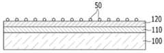
도 1a를 참고하면, 기판(100) 위에 버퍼층(110)을 형성한다. 기판(100)은 유리, 석영, 세라믹, 플라스틱, 및 금속 등 다양한 소재로 제조될 수 있다.Referring to FIG. 1A, a
버퍼층(110)은 질화규소(SiNx)의 단일막 또는 질화규소(SiNx)와 산화규소(SiO2)가 적층된 이중막 구조로 형성된다. 버퍼층(110)은 불순 원소 또는 수분과 같은 불필요한 성분이 상부층으로 침투하는 것을 방지하며, 표면을 평탄화시키는 역할을 한다. 버퍼층(110)은 기판(100)의 종류 및 공정 조건에 따라 생략될 수 있다.The
이어서 버퍼층(110) 위에 비정질 규소막(120)을 형성한다. 비정질 규소막(120)은 예컨대 실란(silane) 가스를 이용한 화학기상증착(CVD)법으로 형성될 수 있다.Subsequently, an
도 1b를 참고하면, 비정질 규소막(120) 위에 금속 촉매(50)를 흡착한다. 금속 촉매(50)의 흡착은 이온 도핑, 증착, 스퍼터링, 코팅, 또는 주입(implantation) 등의 방법으로 이루어질 수 있다. 금속 촉매(50)는 예를 들어 1X10¹⁰ atoms/cm2 내지 1 X 10¹⁴ atoms/cm2 범위 내의 도즈(dose)량으로 미량 흡착될 수 있다.Referring to FIG. 1B, the
금속 촉매(50)는 예를 들어 니켈(Ni), 은(Ag), 금(Au), 구리(Cu), 알루미늄(Al), 주석(Sn), 카드뮴(Cd), 팔라듐(Pd), 이들의 합금 또는 이들의 조합에서 선택될 수 있다.The
이어서 비정질 규소막(120)을 열처리한다. 열처리에 의해 비정질 규소막(120)에 흡착된 금속 촉매(50)가 씨드(seed)로 작용하여 결정이 성장하며, 그 결과 도 1c에 도시한 바와 같이 다결정 규소막(130)이 형성된다.Subsequently, the
니켈(Ni)을 금속 촉매로 사용하여 비정질 규소막(120)을 결정화하는 경우, 니켈은 비정질 규소막(120)의 규소와 반응하여 니켈-실리사이드(NiSix; x=0.5~2)를 형성하고, 니켈-실리사이드가 씨드로 작용하여 이를 중심으로 결정이 성장한다.When the
금속 촉매(50)를 이용한 결정화 방법은 비정질 규소막(120)을 상대적으로 저온에서 빠른 시간에 결정화할 수 있다. 금속 촉매(50)를 이용하여 결정화된 다결정 규소막(130)에는 십수 내지 수십 마이크로미터(㎛) 크기의 그레인(grain)이 형성되며, 이때 그레인 바운더리(grain boundary)에는 금속 촉매(50)가 잔류한다.In the crystallization method using the
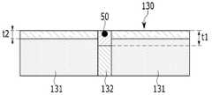
도 1d는 도 1c에 도시한 다결정 규소막의 평면을 나타낸 개략도이고, 도 1e는 도 1c에 도시한 다결정 규소막의 확대 단면도이다.FIG. 1D is a schematic view showing a plane of the polycrystalline silicon film shown in FIG. 1C, and FIG. 1E is an enlarged cross-sectional view of the polycrystalline silicon film shown in FIG. 1C.
도 1d와 도 1e에서 다결정 규소막(130)은 그레인 내부 영역(131)과 그레인 바운더리(132)로 구분되며, 그레인 바운더리(132)에 금속 촉매(50), 예를 들어 니켈이 잔류한다. 그레인 바운더리(132)에 남은 금속 촉매(50)는 결함으로 작용하여 박막 트랜지스터의 누설 전류를 증가시키므로 금속 촉매(50)를 제거해야 한다.In FIGS. 1D and 1E, the
도 1f를 참고하면, 그레인 내부 영역(131)과 그레인 바운더리(132)의 산화 선택비가 다른 에천트를 준비하고, 이 에천트를 이용하여 다결정 규소막(130)의 표면을 식각한다.Referring to FIG. 1F, an etchant having a different oxidation selectivity between the grain
에천트는 불산(HF)과 중크롬산칼륨(K2Cr2O7)의 혼합 용액으로 이루어진다. 에천트 중 중크롬산칼륨은 규소 산화제로서 그레인 바운더리(132)를 산화시키는 속도가 그레인 내부 영역(131)을 산화시키는 속도보다 빠르다. 그리고 불산은 중크롬산칼륨에 의해 산화된 산화규소를 제거하는 역할을 한다.The etchant consists of a mixed solution of hydrofluoric acid (HF) and potassium dichromate (K2 Cr2 O7 ). Potassium dichromate in the etchant oxidizes the
이러한 에천트로 다결정 규소막(130)을 표면 처리하면, 그레인 바운더리(132)의 산화 두께(t1)는 그레인 내부 영역의 산화 두께(t2)보다 크다. 이때 그레인 바운더리(132)의 산화 두께(t1)는 금속 촉매(50)의 크기를 초과한다. 그리고 에천트 중 불산 성분이 그레인 바운더리(132)와 그레인 내부 영역(131)의 산화된 부분을 제거함에 따라, 금속 촉매(50)가 제거된 다결정 규소막(130)을 형성한다.When the
도 1g는 금속 촉매가 제거된 다결정 규소막의 확대 단면도이고, 도 1h는 도 1g에 도시한 다결정 규소막의 평면을 나타낸 개략도이다.FIG. 1G is an enlarged cross-sectional view of the polycrystalline silicon film from which the metal catalyst has been removed, and FIG. 1H is a schematic view showing a plane of the polycrystalline silicon film shown in FIG. 1G.
도 1g와 도 1h를 참고하면, 전술한 에천트로 인해 다결정 규소막(130)에서 그레인 바운더리(132)의 식각 두께는 그레인 내부 영역(131)의 식각 두께보다 크다. 따라서 다결정 규소막(130)에서 금속 촉매가 잔류하고 있던 그레인 바운더리(132)의 상부면 높이는 그레인 내부 영역(131)의 상부면 높이보다 낮게 형성된다.1G and 1H, the etching thickness of the
도 1g와 도 1h에서 도면 부호 55는 그레인 바운더리의 표면에서 금속 촉매가 제거되고 남은 오목부를 나타낸다.In FIGS. 1G and 1H,
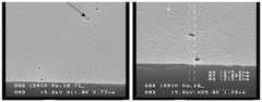
도 2는 전술한 방법으로 형성된 다결정 규소막의 표면을 나타낸 현미경 사진이다. 도 2에서 A는 그레인 내부 영역을 나타내고, B는 그레인 바운더리를 나타내며, C는 잔류 금속 촉매가 제거되고 남은 오목부를 나타낸다.2 is a micrograph showing the surface of the polycrystalline silicon film formed by the above-described method. In FIG. 2, A represents a grain interior region, B represents a grain boundary, and C represents a recess remaining after the residual metal catalyst is removed.
도 3은 도 2에 도시한 그레인 바운더리의 표면을 확대하여 나타낸 주사전자현미경 사진이다.3 is a scanning electron micrograph showing an enlarged surface of the grain boundary shown in FIG. 2.
도 3을 참고하면, 전술한 에천트 처리로 인해 그레인 바운더리에 잔류하고 있던 금속 촉매가 모두 제거되고, 금속 촉매가 제거된 위치마다 금속 촉매의 잔류 위치에 대응하는 오목부가 형성된 것을 확인할 수 있다. 도 3의 왼쪽 사진에서 화살표가 오목부를 가리키고 있다.Referring to FIG. 3, it can be seen that, due to the etchant treatment described above, all metal catalysts remaining in the grain boundary are removed, and recesses corresponding to the remaining positions of the metal catalysts are formed at positions where the metal catalysts are removed. In the left photograph of FIG. 3, the arrow points to the recess.
이와 같이 본 실시예에 따른 다결정 규소막(130) 형성 방법에 따르면, 비정질 규소막(120)의 결정화 이후 그레인 바운더리(132)에 잔류하는 금속 촉매(50)를 효과적으로 제거할 수 있다. 따라서 다결정 규소막(130)을 액티브층으로 사용하는 박막 트랜지스터는 결함으로 작용하는 금속 촉매가 없으므로 누설 전류가 발생하지 않으며, 그 결과 전기적 특성을 향상시킬 수 있다.As described above, according to the method of forming the
이어서 전술한 방법으로 형성된 다결정 규소막(130)을 액티브층으로 사용하는 박막 트랜지스터에 대해 설명한다.Next, a thin film transistor using the
도 4는 본 발명의 일 실시예에 따른 박막 트랜지스터의 단면도이다.4 is a cross-sectional view of a thin film transistor according to an exemplary embodiment of the present invention.
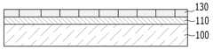
도 4를 참고하면, 기판(100) 위에 버퍼층(110)이 형성되고, 버퍼층(110) 위에 다결정 규소막(130)이 형성된다. 다결정 규소막(130)은 전술한 방법에 따라 금속 촉매를 사용하여 결정화된 것으로서, 전술한 에천트 처리에 의해 그레인 바운더리에 금속 촉매가 잔류하지 않는다.Referring to FIG. 4, a
다결정 규소막(130)은 소정 형상으로 패터닝되어 액티브층으로 사용된다. 다결정 규소막(130)은 채널 영역(130a)과 소스 영역(130b) 및 드레인 영역(130c)을 포함한다. 소스 영역(130b)과 드레인 영역(130c)에는 p형 불순물 또는 n형 불순물이 도핑될 수 있다.The
다결정 규소막(130)을 덮으면서 버퍼층(110) 위에 게이트 절연막(140)이 형성되고, 채널 영역(130a)에 대응하는 게이트 절연막(140) 위에 게이트 전극(145)이 형성된다. 게이트 전극(145)은 다결정 규소막(130)으로 p형 불순물 또는 n형 불순물을 도핑할 때, 채널 영역(130a)에 불순물이 도핑되지 않도록 하는 차단 마스크로 기능한다.The
게이트 전극(145)을 덮으면서 게이트 절연막(140) 위에 층간 절연막(150)이 형성된다. 층간 절연막(150)과 게이트 절연막(140)에는 소스 영역(130b)과 드레인 영역(130c)을 노출시키는 컨택 홀이 형성된다. 층간 절연막(150) 위에는 컨택 홀을 통해 소스 영역(130b)과 연결되는 소스 전극(151) 및 컨택 홀을 통해 드레인 영역(130c)과 연결되는 드레인 전극(152)이 형성된다.An interlayer insulating
전술한 박막 트랜지스터(200)는 금속 촉매가 제거된 다결정 규소막(130)을 액티브층으로 사용하므로 액티브층에 캐리어를 트랩하는 결함이 존재하지 않는다. 따라서 본 실시예에 따른 박막 트랜지스터(200)는 누설 전류가 발생하지 않으며, 문턱 전압이 높아지는 현상도 예방할 수 있다.Since the
도 5는 전술한 박막 트랜지스터를 사용하는 표시 장치를 나타낸 단면도이다. 도 5에서는 표시 장치의 일례로 유기 발광 표시 장치를 도시하였다.5 is a cross-sectional view illustrating a display device using the above-described thin film transistor. 5 illustrates an organic light emitting display device as an example of a display device.
유기 발광 표시 장치(300)는, 복수의 신호선과 연결되어 있으며 대략 행렬(matrix)의 형태로 배열된 복수의 화소(pixel)를 포함한다. 도 5는 복수의 화소 중 하나의 화소를 도시한 것이며, 각 화소는 복수의 박막 트랜지스터를 포함하나 여기에서는 설명의 편이상 하나의 박막 트랜지스터(200)만을 도시한다.The organic light emitting
도 5를 참고하면, 기판(100) 위에 버퍼층(110)이 형성되고, 버퍼층(110) 위에 다결정 규소막(130)이 형성된다. 다결정 규소막(130)은 전술한 방법에 따라 금속 촉매를 사용하여 결정화된 것이며, 전술한 에천트 처리에 의해 그레인 바운더리에 금속 촉매가 잔류하지 않는다.Referring to FIG. 5, a
다결정 규소막(130)은 소정 형상으로 패터닝되어 액티브층으로 사용된다. 다결정 규소막(130)은 채널 영역(130a)과 소스 영역(130b) 및 드레인 영역(130c)을 포함한다. 소스 영역(130b)과 드레인 영역(130c)에는 p형 불순물 또는 n형 불순물이 도핑될 수 있다.The
다결정 규소막(130)을 덮으면서 버퍼층(110) 위에 게이트 절연막(140)이 형성되고, 채널 영역(130a)에 대응하는 게이트 절연막(140) 위에 게이트 전극(145)이 형성된다. 그리고 게이트 전극(145)을 덮으면서 게이트 절연막(140) 위에 층간 절연막(150)이 형성된다. 층간 절연막(150)과 게이트 절연막(140)에는 소스 영역(130b)과 드레인 영역(130c)을 노출시키는 컨택 홀이 형성된다.The
층간 절연막(150) 위에는 컨택 홀을 통해 소스 영역(130b)과 연결되는 소스 전극(151) 및 컨택 홀을 통해 드레인 영역(130c)과 연결되는 드레인 전극(152)이 형성된다. 소스 전극(151)과 드레인 전극(152)을 덮으면서 층간 절연막(150) 위에 평탄화막(160)이 형성되며, 평탄화막(160)에는 드레인 전극(152)을 노출시키는 컨택 홀이 형성된다.A
평탄화막(160) 위에는 컨택 홀을 통해 드레인 전극(152)과 연결되는 화소 전극(171)이 형성되고, 화소 전극(171)을 덮으면서 평탄화막(160) 위에 화소 정의막(165)이 형성된다. 화소 정의막(165)에는 화소 전극(171)의 일부를 노출시키는 개구부가 형성된다.The
화소 정의막(165)의 개구부에는 유기 발광층(172)이 형성되고, 유기 발광층(172)을 덮으면서 화소 정의막(165) 전체에 공통 전극(173)이 형성된다. 화소 전극(171)과 공통 전극(173) 중 어느 하나는 전자 주입 전극(캐소드 전극)으로 기능하고, 다른 하나는 정공 주입 전극(애노드 전극)으로 기능한다.The
유기 발광층(172)은 적색, 녹색, 및 청색 중 어느 한 색상의 빛을 내는 유기 물질 또는 유기 물질과 무기 물질의 혼합물로 형성된다. 유기 발광층(172)의 하부 및 상부에는 유기 발광층(172)의 발광 효율을 개선하기 위한 보조층이 형성될 수 있다. 보조층은 정공 주입층, 정공 수송층, 전자 주입층, 및 전자 수송층 가운데 적어도 하나일 수 있다.The organic
화소 전극(171)과 공통 전극(173) 중 어느 하나는 투명 도전막으로 형성되고, 다른 하나는 반사형 도전막으로 형성될 수 있다. 유기 발광층(172)에서 방출된 빛은 반사형 도전막에 의해 반사되고, 투명 도전막을 투과해 표시 장치 외부로 방출된다. 화소 전극(171)과 유기 발광층(172) 및 공통 전극(173)이 유기 발광 소자(170)를 구성한다.One of the
상기에서는 유기 발광 표시 장치에 대해 설명하였으나, 본 실시예에 따른 표시 장치는 액정 표시 장치일 수 있다. 이때 액정 표시 장치는 액정층(도시하지 않음)을 포함하며, 해당 기술 분야의 종사자에게 공지된 다양한 구조로 형성될 수 있다.Although the OLED display has been described above, the display device according to the present embodiment may be a liquid crystal display device. In this case, the liquid crystal display may include a liquid crystal layer (not shown), and may be formed in various structures known to those skilled in the art.
상기에서는 본 발명의 바람직한 실시예에 대하여 설명하였지만, 본 발명은 이에 한정되는 것이 아니고 특허청구범위와 발명의 상세한 설명 및 첨부한 도면의 범위 안에서 여러 가지로 변형하여 실시하는 것이 가능하고 이 또한 본 발명의 범위에 속하는 것은 당연하다.While the present invention has been described in connection with what is presently considered to be practical exemplary embodiments, it is to be understood that the invention is not limited to the disclosed embodiments, but, on the contrary, Of course.
100: 기판110: 버퍼층
120: 비정질 규소막130: 다결정 규소막
131: 그레인 내부 영역132: 그레인 바운더리
50: 촉매 금속55: 오목부
200: 박막 트랜지스터300: 표시 장치100: substrate 110: buffer layer
120: amorphous silicon film 130: polycrystalline silicon film
131: grain interior area 132: grain boundary
50: catalyst metal 55: recess
200: thin film transistor 300: display device
Claims (12)
Translated fromKorean상기 비정질 규소막 위에 금속 촉매를 흡착하는 단계;
열처리를 통해 상기 비정질 규소막을 결정화하여 그레인 내부 영역과 상기 금속 촉매가 잔류된 그레인 바운더리를 포함하는 다결정 규소막을 형성하는 단계;
상기 그레인 내부 영역 및 상기 그레인 바운더리의 산화 선택비가 다른 에천트를 준비하는 단계; 및
상기 에천트로 상기 다결정 규소막의 표면을 식각하여 상기 그레인 바운더리에 잔류된 금속 촉매를 제거하는 단계
를 포함하는 다결정 규소막의 형성 방법.Forming an amorphous silicon film on the substrate;
Adsorbing a metal catalyst on the amorphous silicon film;
Crystallizing the amorphous silicon film through heat treatment to form a polycrystalline silicon film including an internal region of grain and a grain boundary in which the metal catalyst remains;
Preparing an etchant having a different oxidation selectivity between the grain inner region and the grain boundary; And
Etching the surface of the polycrystalline silicon film with the etchant to remove the metal catalyst remaining in the grain boundary.
Method of forming a polycrystalline silicon film comprising a.
상기 금속 촉매는 니켈(Ni)을 포함하며, 상기 열처리 과정에서 니켈-실리사이드가 씨드로 작용하여 결정화가 이루어지는 다결정 규소막의 형성 방법.The method of claim 1,
The metal catalyst includes nickel (Ni), and nickel-silicide acts as a seed during the heat treatment process to form a polycrystalline silicon film is crystallized.
상기 에천트는 상기 그레인 바운더리의 산화 속도가 상기 그레인 내부 영역의 산화 속도보다 빠른 산화제를 포함하는 다결정 규소막의 형성 방법.The method of claim 1,
And the etchant comprises an oxidant whose oxidation rate of the grain boundary is faster than the oxidation rate of the inner region of the grain.
상기 에천트는 상기 산화제로서 중크롬산칼륨(K2Cr2O7)과, 산화규소를 제거하는 불산(HF)을 포함하는 다결정 규소막의 형성 방법.The method of claim 3,
And the etchant comprises potassium dichromate (K2 Cr2 O7 ) as the oxidant and hydrofluoric acid (HF) to remove silicon oxide.
상기 다결정 규소막에서 상기 그레인 바운더리의 식각 두께는 상기 그레인 내부 영역의 식각 두께보다 큰 다결정 규소막의 형성 방법.The method of claim 3,
And the etching thickness of the grain boundary in the polycrystalline silicon film is larger than the etching thickness of the grain inner region.
상기 그레인 바운더리의 표면에는 상기 금속 촉매가 제거되고 남은 오목부가 형성되는 다결정 규소막의 형성 방법.6. The method of claim 5,
The method of forming a polysilicon film on the surface of the grain boundary, the metal catalyst is removed and the remaining recess is formed.
상기 다결정 규소막 위에 형성되는 게이트 절연막;
상기 게이트 절연막 위에 형성되며 상기 다결정 규소막과 중첩되는 게이트 전극; 및
상기 게이트 전극과 이격되며 상기 다결정 규소막과 전기적으로 연결되는 소스 전극 및 드레인 전극
을 포함하는 박막 트랜지스터.A polycrystalline silicon film formed according to any one of claims 1 to 6;
A gate insulating film formed on the polycrystalline silicon film;
A gate electrode formed on the gate insulating film and overlapping the polycrystalline silicon film; And
Source and drain electrodes spaced apart from the gate electrode and electrically connected to the polycrystalline silicon film
Lt; / RTI >
상기 다결정 규소막 위에 형성되는 게이트 절연막;
상기 게이트 절연막 위에 형성되며 상기 다결정 규소막과 중첩되는 게이트 전극; 및
상기 게이트 전극과 이격되며 상기 다결정 규소막과 전기적으로 연결되는 소스 전극 및 드레인 전극
을 포함하는 박막 트랜지스터.A polycrystalline silicon film including a grain inner region and a grain boundary formed with a recess corresponding to the remaining position of the metal catalyst;
A gate insulating film formed on the polycrystalline silicon film;
A gate electrode formed on the gate insulating film and overlapping the polycrystalline silicon film; And
Source and drain electrodes spaced apart from the gate electrode and electrically connected to the polycrystalline silicon film
Lt; / RTI >
상기 다결정 규소막 위에 형성되는 게이트 절연막;
상기 게이트 절연막 위에 형성되며 상기 다결정 규소막과 중첩되는 게이트 전극; 및
상기 게이트 전극과 이격되며 상기 다결정 규소막과 전기적으로 연결되는 소스 전극 및 드레인 전극
을 포함하는 표시 장치.A polycrystalline silicon film formed according to any one of claims 1 to 6;
A gate insulating film formed on the polycrystalline silicon film;
A gate electrode formed on the gate insulating film and overlapping the polycrystalline silicon film; And
Source and drain electrodes spaced apart from the gate electrode and electrically connected to the polycrystalline silicon film
.
상기 드레인 전극과 전기적으로 연결되는 화소 전극;
상기 화소 전극과 마주하는 공통 전극; 및
상기 화소 전극과 상기 공통 전극 사이에 위치하는 유기 발광층
을 더 포함하는 표시 장치.10. The method of claim 9,
A pixel electrode electrically connected to the drain electrode;
A common electrode facing the pixel electrode; And
An organic emission layer disposed between the pixel electrode and the common electrode
Further comprising:
상기 다결정 규소막 위에 형성되는 게이트 절연막;
상기 게이트 절연막 위에 형성되며 상기 다결정 규소막과 중첩되는 게이트 전극; 및
상기 게이트 전극과 이격되며 상기 다결정 규소막과 전기적으로 연결되는 소스 전극 및 드레인 전극
을 포함하는 표시 장치.A polycrystalline silicon film including a grain inner region and a grain boundary formed with a recess corresponding to the remaining position of the metal catalyst;
A gate insulating film formed on the polycrystalline silicon film;
A gate electrode formed on the gate insulating film and overlapping the polycrystalline silicon film; And
Source and drain electrodes spaced apart from the gate electrode and electrically connected to the polycrystalline silicon film
.
상기 드레인 전극과 전기적으로 연결되는 화소 전극;
상기 화소 전극과 마주하는 공통 전극; 및
상기 화소 전극과 상기 공통 전극 사이에 위치하는 유기 발광층
을 더 포함하는 표시 장치.12. The method of claim 11,
A pixel electrode electrically connected to the drain electrode;
A common electrode facing the pixel electrode; And
An organic emission layer disposed between the pixel electrode and the common electrode
Further comprising:
Priority Applications (4)
| Application Number | Priority Date | Filing Date | Title |
|---|---|---|---|
| KR1020120106640AKR20140039863A (en) | 2012-09-25 | 2012-09-25 | Method for forming polycrystalline silicon layer, thin film transistor and display device with the polycrystalline silicon layer |
| US13/962,105US20140084268A1 (en) | 2012-09-25 | 2013-08-08 | Method of forming polysilicon film, thin film transistor and display device including polysilicon film |
| CN201310348944.3ACN103681349A (en) | 2012-09-25 | 2013-08-12 | Method of forming polysilicon film, thin film transistor and display device |
| TW102129085ATW201413978A (en) | 2012-09-25 | 2013-08-14 | Method for forming polycrystalline germanium film, thin film transistor comprising polycrystalline germanium film, and display device comprising polycrystalline germanium film |
Applications Claiming Priority (1)
| Application Number | Priority Date | Filing Date | Title |
|---|---|---|---|
| KR1020120106640AKR20140039863A (en) | 2012-09-25 | 2012-09-25 | Method for forming polycrystalline silicon layer, thin film transistor and display device with the polycrystalline silicon layer |
Publications (1)
| Publication Number | Publication Date |
|---|---|
| KR20140039863Atrue KR20140039863A (en) | 2014-04-02 |
Family
ID=50318535
Family Applications (1)
| Application Number | Title | Priority Date | Filing Date |
|---|---|---|---|
| KR1020120106640AWithdrawnKR20140039863A (en) | 2012-09-25 | 2012-09-25 | Method for forming polycrystalline silicon layer, thin film transistor and display device with the polycrystalline silicon layer |
Country Status (4)
| Country | Link |
|---|---|
| US (1) | US20140084268A1 (en) |
| KR (1) | KR20140039863A (en) |
| CN (1) | CN103681349A (en) |
| TW (1) | TW201413978A (en) |
Cited By (1)
| Publication number | Priority date | Publication date | Assignee | Title |
|---|---|---|---|---|
| KR20160017839A (en)* | 2014-08-06 | 2016-02-17 | 삼성디스플레이 주식회사 | Thin film transistor, display apparatus comprising the same, method for manufacturing thin film transistor, and method for manufacturing display apparatus |
Family Cites Families (18)
| Publication number | Priority date | Publication date | Assignee | Title |
|---|---|---|---|---|
| TW279275B (en)* | 1993-12-27 | 1996-06-21 | Sharp Kk | |
| KR100653263B1 (en)* | 2000-12-29 | 2006-12-01 | 엘지.필립스 엘시디 주식회사 | Crystallization Method of Silicon Film |
| KR100466964B1 (en)* | 2001-12-27 | 2005-01-24 | 엘지.필립스 엘시디 주식회사 | Method of manufacturing for poly-Silicone thin layer |
| US6727122B2 (en)* | 2001-12-29 | 2004-04-27 | Lg. Philips Lcd Co., Ltd. | Method of fabricating polysilicon thin film transistor |
| US6930326B2 (en)* | 2002-03-26 | 2005-08-16 | Semiconductor Energy Laboratory Co., Ltd. | Semiconductor circuit and method of fabricating the same |
| JP4115252B2 (en)* | 2002-11-08 | 2008-07-09 | シャープ株式会社 | Semiconductor film and manufacturing method thereof, and semiconductor device and manufacturing method thereof |
| KR100656495B1 (en)* | 2004-08-13 | 2006-12-11 | 삼성에스디아이 주식회사 | Thin film transistor and its manufacturing method |
| JP2006261632A (en)* | 2005-02-18 | 2006-09-28 | Sumco Corp | Method of thermally treating silicon wafer |
| KR100700494B1 (en)* | 2005-08-25 | 2007-03-28 | 삼성에스디아이 주식회사 | Thin film transistor and its manufacturing method |
| JP2007266466A (en)* | 2006-03-29 | 2007-10-11 | Tokyo Electron Ltd | Plasma etching method, plasma etching apparatus, computer storage medium, and storage medium with treatment recipe stored thereon |
| KR100770269B1 (en)* | 2006-05-18 | 2007-10-25 | 삼성에스디아이 주식회사 | Method of manufacturing thin film transistor |
| KR101049805B1 (en)* | 2008-12-30 | 2011-07-15 | 삼성모바일디스플레이주식회사 | Method for manufacturing polycrystalline silicon, thin film transistor, method for manufacturing same, and organic light emitting display device comprising the same |
| KR101049799B1 (en)* | 2009-03-03 | 2011-07-15 | 삼성모바일디스플레이주식회사 | Thin film transistor, manufacturing method thereof and organic light emitting display device comprising same |
| US8003431B2 (en)* | 2009-10-21 | 2011-08-23 | Electronics And Telecommunications Research Institute | Method for antireflection treatment of a zinc oxide film and method for manufacturing solar cell using the same |
| KR101125565B1 (en)* | 2009-11-13 | 2012-03-23 | 삼성모바일디스플레이주식회사 | Thin Film Transistor, The Organic light Emitting Display Device Comprising The TFT and the Fabricating Methods of the Same |
| KR101049802B1 (en)* | 2009-11-20 | 2011-07-15 | 삼성모바일디스플레이주식회사 | Method for manufacturing polycrystalline silicon layer, thin film transistor, organic light emitting display device having same and method for manufacturing thereof |
| KR101117643B1 (en)* | 2010-04-08 | 2012-03-05 | 삼성모바일디스플레이주식회사 | Crystallization method of amorphous silicon layer, and thin film transistor and method for the same |
| KR101050467B1 (en)* | 2010-04-14 | 2011-07-20 | 삼성모바일디스플레이주식회사 | A polycrystalline silicon layer, a manufacturing method thereof, a thin film transistor using the polycrystalline silicide layer, and an organic light emitting display device having the thin film transistor |
- 2012
- 2012-09-25KRKR1020120106640Apatent/KR20140039863A/ennot_activeWithdrawn
- 2013
- 2013-08-08USUS13/962,105patent/US20140084268A1/ennot_activeAbandoned
- 2013-08-12CNCN201310348944.3Apatent/CN103681349A/enactivePending
- 2013-08-14TWTW102129085Apatent/TW201413978A/enunknown
Cited By (1)
| Publication number | Priority date | Publication date | Assignee | Title |
|---|---|---|---|---|
| KR20160017839A (en)* | 2014-08-06 | 2016-02-17 | 삼성디스플레이 주식회사 | Thin film transistor, display apparatus comprising the same, method for manufacturing thin film transistor, and method for manufacturing display apparatus |
Also Published As
| Publication number | Publication date |
|---|---|
| CN103681349A (en) | 2014-03-26 |
| US20140084268A1 (en) | 2014-03-27 |
| TW201413978A (en) | 2014-04-01 |
Similar Documents
| Publication | Publication Date | Title |
|---|---|---|
| KR100889626B1 (en) | Thin film transistor, manufacturing method thereof, organic light emitting display device having same, and manufacturing method thereof | |
| US7999261B2 (en) | Thin film transistor, method of fabricating the same, and organic light emitting diode display device having the TFT | |
| US8283668B2 (en) | Thin film transistor, method of fabricating the same, and organic light emitting diode display device including the same | |
| KR100882909B1 (en) | Thin film transistor, manufacturing method thereof, organic light emitting display device comprising same, and manufacturing method thereof | |
| KR100982310B1 (en) | TFT, fabricating methode of the TFT, and organic lighting emitting diode display device comprising the same | |
| EP2226833B1 (en) | Method of fabricating a thin film transistor | |
| US8318523B2 (en) | Thin film transistor, method of fabricating the same and organic light emitting diode display device having the same | |
| KR100878284B1 (en) | Thin film transistor, manufacturing method thereof and organic light emitting display device having same | |
| US7994706B2 (en) | Organic light emitting diode display device and method of fabricating the same | |
| JP2011048339A (en) | Organic light-emitting display device and method of fabricating the same | |
| CN101330004A (en) | Manufacturing method of polysilicon, thin film transistor and manufacturing method, and organic light-emitting diode display device | |
| WO2013118233A1 (en) | Thin film semiconductor device manufacturing method and thin film semiconductor device | |
| KR100946560B1 (en) | Method of manufacturing thin film transistor | |
| US9112034B2 (en) | Thin-film semiconductor device and method of manufacturing the same | |
| KR101911509B1 (en) | Organic light emitting display device and method for manufacturing the same | |
| KR20140039863A (en) | Method for forming polycrystalline silicon layer, thin film transistor and display device with the polycrystalline silicon layer | |
| US20130015453A1 (en) | Display device, thin-film transistor used for display device, and method of manufacturing thin-film transistor | |
| KR102467402B1 (en) | Method for crystallizing silicon and method for manufacturing a thin film transistor substrate | |
| WO2013118234A1 (en) | Thin film semiconductor device manufacturing method and thin film semiconductor device | |
| KR100943953B1 (en) | Manufacturing method of display device | |
| KR100700496B1 (en) | Thin film transistor and organic light emitting display device using same |
Legal Events
| Date | Code | Title | Description |
|---|---|---|---|
| PA0109 | Patent application | Patent event code:PA01091R01D Comment text:Patent Application Patent event date:20120925 | |
| PG1501 | Laying open of application | ||
| PC1203 | Withdrawal of no request for examination | ||
| WITN | Application deemed withdrawn, e.g. because no request for examination was filed or no examination fee was paid |