KR20140038305A - Processing method - Google Patents
Processing methodDownload PDFInfo
- Publication number
- KR20140038305A KR20140038305AKR1020130105964AKR20130105964AKR20140038305AKR 20140038305 AKR20140038305 AKR 20140038305AKR 1020130105964 AKR1020130105964 AKR 1020130105964AKR 20130105964 AKR20130105964 AKR 20130105964AKR 20140038305 AKR20140038305 AKR 20140038305A
- Authority
- KR
- South Korea
- Prior art keywords
- wafer
- adhesive sheet
- plate
- expanding
- protective member
- Prior art date
- Legal status (The legal status is an assumption and is not a legal conclusion. Google has not performed a legal analysis and makes no representation as to the accuracy of the status listed.)
- Granted
Links
Images


Classifications
- H—ELECTRICITY
- H01—ELECTRIC ELEMENTS
- H01L—SEMICONDUCTOR DEVICES NOT COVERED BY CLASS H10
- H01L21/00—Processes or apparatus adapted for the manufacture or treatment of semiconductor or solid state devices or of parts thereof
- H01L21/02—Manufacture or treatment of semiconductor devices or of parts thereof
- H01L21/04—Manufacture or treatment of semiconductor devices or of parts thereof the devices having potential barriers, e.g. a PN junction, depletion layer or carrier concentration layer
- H01L21/50—Assembly of semiconductor devices using processes or apparatus not provided for in a single one of the groups H01L21/18 - H01L21/326 or H10D48/04 - H10D48/07 e.g. sealing of a cap to a base of a container
- H—ELECTRICITY
- H01—ELECTRIC ELEMENTS
- H01L—SEMICONDUCTOR DEVICES NOT COVERED BY CLASS H10
- H01L21/00—Processes or apparatus adapted for the manufacture or treatment of semiconductor or solid state devices or of parts thereof
- H01L21/67—Apparatus specially adapted for handling semiconductor or electric solid state devices during manufacture or treatment thereof; Apparatus specially adapted for handling wafers during manufacture or treatment of semiconductor or electric solid state devices or components ; Apparatus not specifically provided for elsewhere
- H01L21/683—Apparatus specially adapted for handling semiconductor or electric solid state devices during manufacture or treatment thereof; Apparatus specially adapted for handling wafers during manufacture or treatment of semiconductor or electric solid state devices or components ; Apparatus not specifically provided for elsewhere for supporting or gripping
- H—ELECTRICITY
- H01—ELECTRIC ELEMENTS
- H01L—SEMICONDUCTOR DEVICES NOT COVERED BY CLASS H10
- H01L21/00—Processes or apparatus adapted for the manufacture or treatment of semiconductor or solid state devices or of parts thereof
- H01L21/70—Manufacture or treatment of devices consisting of a plurality of solid state components formed in or on a common substrate or of parts thereof; Manufacture of integrated circuit devices or of parts thereof
- H01L21/77—Manufacture or treatment of devices consisting of a plurality of solid state components or integrated circuits formed in, or on, a common substrate
- H01L21/78—Manufacture or treatment of devices consisting of a plurality of solid state components or integrated circuits formed in, or on, a common substrate with subsequent division of the substrate into plural individual devices
Landscapes
- Engineering & Computer Science (AREA)
- Physics & Mathematics (AREA)
- Condensed Matter Physics & Semiconductors (AREA)
- General Physics & Mathematics (AREA)
- Manufacturing & Machinery (AREA)
- Computer Hardware Design (AREA)
- Microelectronics & Electronic Packaging (AREA)
- Power Engineering (AREA)
- Dicing (AREA)
- Mechanical Engineering (AREA)
- Container, Conveyance, Adherence, Positioning, Of Wafer (AREA)
Abstract
Translated fromKoreanDescription
Translated fromKorean본 발명은 반도체 웨이퍼 등의 얇은 판형물을 다수의 칩으로 분할하는 가공 방법에 관한 것으로, 특히 접착 시트가 점착된 판형물의 가공 방법에 관한 것이다.BACKGROUND OF THE
다수의 디바이스가 표면에 형성된 반도체 웨이퍼 등의 원판형 웨이퍼는, 디바이스 사이의 분할 예정 라인을 따라 분할되어 반도체 칩으로 개편화된다. 그런데, 칩을 실장할 때의 접착층을 미리 이면에 형성해 두기 위해, DAF(Die Attach Film) 등의 접착층 형성용 접착 시트를 웨이퍼의 이면에 점착한 상태로 웨이퍼를 분할하는 기술이 제공되고 있다. 그 경우, 접착 시트는 웨이퍼보다 약간 대직경으로 형성되어 있고, 웨이퍼의 이면에 점착된 접착 시트는 웨이퍼의 외주로부터 일부가 비어져 나와 있다.A disk-shaped wafer such as a semiconductor wafer on which a plurality of devices are formed on the surface is divided along a line to be divided between devices and is divided into semiconductor chips. However, in order to form an adhesive layer on the back surface before mounting the chip, there is provided a technique of dividing the wafer with the adhesive sheet for forming an adhesive layer such as DAF (Die Attach Film) adhered to the back surface of the wafer. In this case, the adhesive sheet is formed to have a slightly larger diameter than that of the wafer, and the adhesive sheet adhered to the back surface of the wafer is partially removed from the outer periphery of the wafer.
접착 시트는 웨이퍼의 분할 시에, 웨이퍼와 함께 분할되지만, 분할 예정 라인을 따른 분할 기점을 갖는 웨이퍼에 점착된 익스팬딩 테이프 등을 확장함으로써 웨이퍼에 외력을 부여하여 웨이퍼를 분할하는 방법을 채용하였을 때에는, 웨이퍼의 외주로부터 비어져 나온 부분도 분단되고, 그때에 생긴 접착 시트의 파단 부스러기가 웨이퍼의 표면에 부착되어 버린다고 하는 문제가 있었다.When the method of dividing the wafer by applying an external force to the wafer by expanding the expanding tape or the like adhered to the wafer having the dividing origin along the line to be divided along the dividing line at the time of dividing the wafer at the time of dividing the wafer is adopted , There is also a problem that the portion which is vacated from the outer periphery of the wafer is also divided and the broken debris of the adhesive sheet formed at that time is adhered to the surface of the wafer.
그래서, 이 문제를 해결하기 위해, 익스팬딩 테이프의 확장중에 에어 블로우 수단으로 웨이퍼 표면에 대하여 공기를 분출하여, 접착 시트의 파단 부스러기가 웨이퍼 표면에 부착되지 않게 하는 기술이 제안되어 있다(특허문헌 1).In order to solve this problem, there has been proposed a technique in which air is blown against the wafer surface by air blowing means during expansion of the expanding tape so that the broken debris of the adhesive sheet is not adhered to the wafer surface (see Patent Document 1 ).
그러나 상기 문헌에 기재된 기술에 의해서도, 접착 시트의 파단 부스러기가 웨이퍼 표면에 부착되는 것을 완전히 방지하는 것은 어려웠다.However, even with the technique described in the above document, it is difficult to completely prevent the rupture debris of the adhesive sheet from adhering to the wafer surface.
본 발명은 상기 사정을 감안하여 이루어진 것으로, 그 주요 기술적 과제는, 이면에 접착 시트를 점착한 웨이퍼 등의 판형물을 확장하여 분할할 때에, 판형물의 표면에 접착 시트의 파단 부스러기가 부착되는 것을 완전히 방지할 수 있는 가공 방법을 제공하는 것이다.DISCLOSURE OF THE INVENTION The present invention has been made in view of the above circumstances, and its main technical problem is that when the plate-like material such as a wafer adhered to the back surface of an adhesive sheet is extended and divided, the peeling debris of the adhesive sheet adheres to the surface of the plate- And to provide a machining method capable of preventing the machining process.
본 발명의 가공 방법은, 표면에 보호 부재가 배치되며 분할 예정 라인을 따라 분할 기점이 형성된 판형물의 가공 방법으로서, 판형물보다 대직경의 접착 시트를 개재하여 판형물을 익스팬딩 테이프 상에 배치하는 점착 단계와, 상기 점착 단계를 실시한 후, 판형물의 표면에 상기 보호 부재가 배치된 상태로 상기 익스팬딩 테이프를 확장하여 판형물의 외주측으로 비어져 나온 상기 접착 시트를 분단하는 제1 확장 단계와, 상기 제1 확장 단계를 실시한 후, 판형물의 표면에 배치된 상기 보호 부재를 제거하는 보호 부재 제거 단계와, 상기 보호 부재 제거 단계를 실시한 후, 상기 익스팬딩 테이프를 확장하여 판형물을 상기 분할 기점으로부터 상기 분할 예정 라인을 따라 분할하며 판형물에 대응하는 상기 접착 시트를 상기 분할 예정 라인을 따라 파단하는 제2 확장 단계를 포함하는 것을 특징으로 한다.A processing method of the present invention is a processing method of a plate-like object having a protective member disposed on a surface thereof and a dividing base point formed along a line to be divided, wherein a plate-like material is placed on an expanding tape via an adhesive sheet having a larger diameter than a plate- A first expanding step of expanding the expanding tape in a state in which the protective member is disposed on the surface of the plate-like object after the adhesion step, and separating the adhesive sheet which has been discharged to the outer periphery side of the plate- A step of removing the protective member disposed on the surface of the plate-shaped object after the first expansion step; and a step of removing the protective member from the division starting point by expanding the expanding tape after the step of removing the protective member, Dividing the adhesive sheet corresponding to the plate-like material along the line to be divided along the line to be divided And a second expansion step.
본 발명의 가공 방법에서는, 판형물의 표면에 보호 부재를 배치한 상태로 제1 확장 단계가 수행되고, 이 시점에서 적어도 판형물의 외주측으로 비어져 나온 접착 시트가 파단된다. 파단 시에 생긴 접착 시트의 파단 부스러기는 보호 부재 상에 부착된다. 제1 확장 단계를 실시한 후, 파단 부스러기가 부착된 보호 부재는 판형물 상에서 제거되기 때문에, 파단 부스러기가 판형물의 표면에 부착하는 것을 완전히 막을 수 있다.In the processing method of the present invention, the first expansion step is carried out with the protective member disposed on the surface of the plate-shaped article, and at this point, the adhesive sheet evacuated to at least the outer periphery side of the plate-shaped article is broken. The rupture debris of the adhesive sheet formed at the time of breaking is attached on the protective member. After carrying out the first expansion step, the protective member with the ruptured debris is removed on the plate, so that the ruptured debris can be completely prevented from adhering to the surface of the plate.
본 발명에서는, 상기 제2 확장 단계를 실시한 후, 판형물이 분할되어 형성된 개개의 칩 사이의 간격을 유지한 상태로 상기 익스팬딩 테이프에 환형 프레임을 점착하고, 상기 환형 프레임의 개구에 판형물이 분할되어 형성된 복수의 상기 칩을 수용한 형태로 하는 환형 프레임 점착 단계를 포함하는 형태를 포함한다. 이 형태에 따르면, 분할 후의 개개의 칩 사이의 간격이 유지되어, 환형 프레임을 핸들링함으로써 칩을 파손시키는 일없이 반송 등을 행할 수 있다.In the present invention, after the second expansion step is performed, the annular frame is adhered to the expansive tape in a state in which the interval between the individual chips formed by dividing the plate-shaped article is maintained, And an annular frame sticking step of holding a plurality of the chips formed in a divided manner. According to this aspect, the interval between the individual chips after the division is maintained, and handling can be carried out without destroying the chip by handling the annular frame.
본 발명에 따르면, 이면에 접착 시트를 점착한 웨이퍼 등의 판형물을 확장하여 분할할 때에, 판형물의 표면에 접착 시트의 파단 부스러기가 부착되는 것을 완전히 방지할 수 있는 가공 방법이 제공된다.According to the present invention, there is provided a processing method capable of completely preventing the adhesive sheet from adhering to the surface of the plate-like material when the plate-shaped object such as a wafer to which the adhesive sheet is adhered is extended and divided.
도 1은 본 발명의 일 실시형태에 따른 가공 방법의 보호 부재 점착 단계를 나타내는 사시도이다.
도 2는 일 실시형태의 가공 방법의 이면 연삭 단계를 나타내는 사시도이다.
도 3은 일 실시형태의 가공 방법의 개질층 형성 단계를 나타내는 사시도이다.
도 4는 개질층 형성 단계의 상세를 나타내는 웨이퍼의 일부 단면도이다.
도 5는 일 실시형태의 가공 방법의 점착 단계를 나타내는 사시도이다.
도 6은 일 실시형태의 가공 방법의 제1 확장 단계를 나타내는 사시도이다.
도 7은 제1 확장 단계를 나타내는 단면도이다.
도 8은 제1 확장 단계 후의 상태를 나타내는 사시도이다.
도 9는 일 실시형태의 가공 방법의 보호 부재 제거 단계를 나타내는 사시도이다.
도 10은 일 실시형태의 가공 방법의 제2 확장 단계를 나타내는 사시도이다.
도 11은 제2 확장 단계를 나타내는 단면도이다.
도 12는 일 실시형태의 가공 방법의 (a) 환형 프레임 점착 단계를 나타내는 단면도, (b) 환형 프레임 점착 단계 후의 익스팬딩 테이프 절단을 나타내는 단면도이다.
도 13은 익스팬딩 테이프 절단 후에 익스팬딩 장치로부터 웨이퍼를 반출한 상태를 나타내는 사시도이다.
도 14는 다른 실시형태의 익스팬딩 장치를 나타내는 단면도로서, (a) 웨이퍼를 세팅한 상태, (b) 제1 확장 단계를 행한 상태, (c) 제2 확장 단계를 행한 상태를 나타내고 있다.BRIEF DESCRIPTION OF THE DRAWINGS FIG. 1 is a perspective view showing a protective member sticking step of a working method according to an embodiment of the present invention; FIG.
Fig. 2 is a perspective view showing a back grinding step of the working method of one embodiment. Fig.
3 is a perspective view showing the modified layer forming step of the working method of one embodiment.
4 is a partial cross-sectional view of the wafer showing the details of the reforming layer forming step.
Fig. 5 is a perspective view showing an adhesion step of the processing method of one embodiment. Fig.
6 is a perspective view showing a first expansion step of the processing method of one embodiment.
7 is a sectional view showing the first expansion step.
8 is a perspective view showing a state after the first expansion step.
Fig. 9 is a perspective view showing the protective member removing step of the working method of one embodiment. Fig.
10 is a perspective view showing a second expansion step of the processing method of one embodiment.
11 is a cross-sectional view showing a second expansion step.
Fig. 12 is a cross-sectional view showing (a) an annular frame sticking step and (b) a cross-sectional view showing an expanding tape cut after the annular frame sticking step in the working method of one embodiment.
13 is a perspective view showing a state in which the wafer is taken out from the expending device after the cutting of the expanding tape.
Fig. 14 is a cross-sectional view of an expending apparatus according to another embodiment. Fig. 14 (a) shows a state in which a wafer is set, (b) in a first expansion step, and (c) in a second expansion step.
이하, 도면을 참조하여 본 발명의 가공 방법을 포함하는 일 실시형태에 따른 웨이퍼의 가공 방법을 설명한다.Hereinafter, a method of processing a wafer according to an embodiment including a processing method of the present invention will be described with reference to the drawings.
(1) 보호 부재 점착 단계(1) Step of sticking protective member
도 1에 나타내는 바와 같이, 반도체 웨이퍼 등의 원판형의 웨이퍼(판형물)(1)의 표면(1a) 전체면에, 보호 부재(11)를 점착한다. 웨이퍼(1)의 표면(도 1에서는 하면측이 표면)(1a)에는 복수의 분할 예정 라인이 격자형으로 설정되고, 분할 예정 라인으로 구획된 복수의 직사각 형상의 각 디바이스 영역에, LSI 등의 전자 회로를 갖는 디바이스(2)가 각각 형성되어 있다. 보호 부재(11)는, 예컨대 가요성을 갖는 수지 시트의 한 면에 점착층이 형성된 것 등이 이용되고, 점착층을 개재하여 웨이퍼(1)의 표면(1a)을 덮어 점착된다. 보호 부재(11)로서는, 실리콘 웨이퍼나 유리 기판, 세라믹스 기판 등의 하드 플레이트를 이용하며, 접착제 등에 의해 웨이퍼에 점착하는 형태여도 좋다.As shown in Fig. 1, the
(2) 이면 연삭 단계(2) backside grinding step
다음에, 도 2에 나타내는 바와 같이, 보호 부재(11)측을 유지 테이블(21)에 맞추어 웨이퍼(1)를 유지 테이블(21)에서 유지하고, 상방에 노출되는 웨이퍼(1)의 이면(1b)을 연삭 수단(22)으로 연삭하여 웨이퍼(1)를 정해진 두께(예컨대 50 ㎛∼100 ㎛ 정도)로 박화한다.Next, as shown in Fig. 2, the
유지 테이블(21)은 다공질 재료에 의해 형성된 원형상의 수평 유지면 상에, 공기 흡인에 의한 부압 작용에 의해 피가공물을 흡착하여 유지하는 일반 주지의 부압 척 테이블이며, 도시하지 않는 회전 구동 기구에 의해 축 둘레로 회전하게 된다. 연삭 수단(22)은, 연직 방향으로 연장되고, 도시하지 않는 모터에 의해 회전 구동되는 스핀들(23)의 선단에, 플랜지(24)를 통해 연삭 휠(25)이 고정된 것으로, 유지 테이블(21)의 상방에 상하 이동 가능하게 배치되어 있다. 연삭 휠(25)의 하면 외주부에는, 다수의 지석(26)이 환형으로 배열되어 고착되어 있다. 지석(26)은 웨이퍼(1)의 재질에 따른 것이 이용되며, 예컨대 다이아몬드의 지립을 메탈 본드나 레진 본드 등의 결합제로 굳혀 성형한 다이아몬드 지석 등이 이용된다.The holding table 21 is a commonly known negative pressure chuck table for holding and holding a workpiece by a negative pressure action by air suction on a circular horizontal holding surface formed by a porous material, And is rotated about the axis. The grinding means 22 has a
연삭 단계에서는, 보호 부재(11)측을 유지면에 맞추어 웨이퍼(1)를 유지 테이블(21) 상에 배치하고, 부압 척에 의해 웨이퍼(1)를 흡착 유지한다. 그리고, 유지 테이블(21)을 정해진 속도로 한 방향으로 회전시킨 상태에서 연삭 수단(22)을 하강시켜, 회전하는 연삭 휠(25)의 지석(26)을 웨이퍼(1)의 이면(1b)에 압박하여, 이면(1b) 전체면을 연삭한다.In the grinding step, the
(3) 개질층 형성 단계(3) Modification layer formation step
다음에, 웨이퍼(1)에 대하여 투과성을 갖는 파장의 레이저 빔을 분할 예정 라인을 따라 조사하여, 웨이퍼(1)의 내부에 분할 예정 라인을 따른 개질층을 형성한다. 개질층의 형성은, 도 3에 나타내는 바와 같이, 상기 유지 테이블(21)과 같은 회전 가능한 부압 척식의 유지 테이블(31)의 유지면에 보호 보재(11)측을 맞추어 웨이퍼(1)를 유지 테이블(31) 상에 배치하고, 부압 척에 의해 웨이퍼(1)를 흡착 유지한다. 그리고, 유지 테이블(31)의 상방에 배치된 레이저 조사 수단(32)의 조사부(33)로부터, 도 4에 나타내는 바와 같이 웨이퍼(1)에 대하여 투과성을 갖는 파장의 레이저 빔(L)을, 연삭된 이면(1b)측으로부터, 집광점을 웨이퍼(1)의 내부에 위치시킨 상태로 분할 예정 라인을 따라 조사하여, 개질층(1c)을 형성한다.Next, a laser beam of a wavelength having a transmittance to the
유지 테이블(31)은 도 3에 나타내는 X 방향 및 Y 방향으로 이동 가능하게 되며, 웨이퍼(1)에 대한 레이저 빔(L)의 주사는, 예컨대 유지 테이블(31)을 X 방향으로 이동시키는 가공 이송에 의해 이루어진다. 그 경우, 유지 테이블(31)을 Y 방향으로 이동시키는 인덱싱 이송에 의해 레이저 빔(L)을 조사하는 분할 예정 라인을 선택한다. 또한, 분할 예정 라인을 X 방향을 따른 상태로 하기 위해서는, 유지 테이블(31)을 회전시킨다. 개질층(1c)은 레이저 빔(L)의 피조사면[웨이퍼(1)의 이면(1b)]으로부터 일정 깊이의 위치에 일정한 층두께로 형성되도록 한다. 개질층(1c)은 웨이퍼(1) 내의 다른 부분보다 강도가 저하하는 특성을 가지며, 이후의 제2 확장 단계에서 웨이퍼(1)의 분할 기점이 된다.The holding table 31 can be moved in the X and Y directions shown in Fig. 3 and the scanning of the laser beam L on the
(4) 점착 단계(4) Adhesion step
다음에, 도 5에 나타내는 바와 같이, 웨이퍼(1)보다 대직경의 접착 시트(12)를 개재하여 웨이퍼(1)의 이면(1b)측을 익스팬딩 테이프(13) 상에 배치한다. 익스팬딩 테이프(13)는, 예컨대 폴리염화비닐이나 폴리올레핀 등의 신축성을 갖는 합성 수지 시트 등의 한 면에 점착층이 형성된 것으로, 이 경우, 웨이퍼(1)보다 큰 직사각 형상의 것이나 롤형으로 권취된 것이 이용된다.5, the
점착 단계는, 익스팬딩 테이프(13)의 점착층측에, DAF 등으로 이루어지는 접착 시트(12)를 원형상으로 배치하고, 계속해서 그 접착 시트(12) 상에, 웨이퍼(1)의 이면(1b)측을 맞추어 점착한다. 또한, 미리 원형상의 접착 시트(12)가 배치되어 있는 익스팬팅 테이프(13)에 웨이퍼(1)를 점착하여도 좋다. 혹은, 웨이퍼(1)의 이면(1b)에 접착 시트(12)를 점착하고, 그 접착 시트(12)를 익스팬딩 테이프(13)의 점착층에 점착하여도 좋다. 접착 시트(12)는 웨이퍼(1)보다 대직경의 원형상으로 형성되고, 웨이퍼(1)의 외주측에는 접착 시트(12)의 과잉부(12a)가 표출되는 상태가 된다.The adhesive step is carried out in such a manner that an
(5) 제1 확장 단계(5) First Expansion Phase
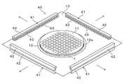
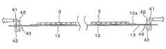
다음에, 웨이퍼(1)의 표면(1a)에 보호 부재(11)가 배치된 상태로 익스팬딩 테이프(13)를 확장하여, 웨이퍼(1)의 외주측으로 비어져 나온 접착 시트(12)의 과잉부(12a)를 분단한다.Next, the expanding
제1 확장 단계에서는, 도 6 및 도 7에 나타내는 익스팬딩 장치(40)를 이용한다. 익스팬딩 장치(40)는, 익스팬딩 테이프(13)의 4변의 단 가장자리를 각각 파지하여, 단 가장자리에 직교하는 외측으로 인장하는 클램프 부재(41)를 갖고 있다. 클램프 부재(41)는 단면 L자형의 프레임(42)을 상하 대칭의 상태로 조합한 구성이며, 각 프레임(42)의 내측에는, 복수의 롤러(43)가 근접하여 배열되어 있다. 이들 롤러(43)는 프레임(42)의 길이 방향에 직교하는 회전축을 중심으로 하여 회전 가능하게 프레임(42)에 지지되어 있다. 익스팬딩 테이프(13)는 상하의 롤러(43) 사이에 협지되고, 협지된 상태에 있어서 익스팬딩 테이프(13)가 단 가장자리를 따른 방향으로 연신되면, 그것에 추종하여 롤러(43)는 전동한다.In the first expansion step, the
익스팬딩 테이프(13)의 확장은, 우선, 익스팬딩 장치(40)의 각 클램프 부재(41)의 상하의 프레임(42) 사이에 익스팬딩 테이프(13)의 4변의 단 가장자리를 통과시키고, 상하의 프레임(42)을 서로 근접시켜 상하의 롤러(43)로 익스팬딩 테이프(13)를 협지한다. 계속해서 클램프 부재(41)를 외측(도 6 및 도 7의 화살표 방향)으로 이동시켜 익스팬딩 테이프(13)를 확장한다. 클램프 부재(41)의 롤러(43)로 협지하고 있기 때문에, 확장에 의해 치우친 변형이 익스팬딩 테이프(13)에 생겨도, 롤러(43)가 전동함으로써 그 변형은 해방되고, 익스팬딩 테이프(13)는 균일하게 확장된다.Expansion of the
이와 같이 익스팬딩 테이프(13)를 확장함으로써, 도 8에 나타내는 바와 같이 웨이퍼(1)의 외주측으로 비어져 나온 접착 시트(12)의 과잉부(12a)만을 분단한다. 여기서는, 아직 웨이퍼(1)를 분할하지 않고, 과잉부(12a)가 분단될 정도까지 익스팬딩 테이프(13)를 확장한다.By expanding the expanding
과잉부(12a)를 분단시킬 때에는, 적어도 과잉부(12a)를 냉각해 두면 분단하기 쉽기 때문 바람직하다. 과잉부(12a)를 냉각하기 위해서는, 예컨대 표면측으로부터 직접, 혹은 이면측의 익스팬딩 테이프(13)를 개재하여 과잉부(12a)에 냉각시킨 에어 등의 냉각 유체를 분출함으로써 가능하다. 또한, 익스팬딩 장치(40) 전체를 냉각 챔버 내에 수용하고, 냉각 챔버 내의 분위기 온도를 예컨대 0℃∼-30℃ 정도로 설정하여 전체를 냉각한 상태로 확장한다고 하는 방법을 채용하여도 좋다.When separating the
과잉부(12a)가 분단되면, 도 8에 나타내는 바와 같이 과잉부(12a)로부터 접착 시트(12)의 파단 부스러기(12b)가 생기지만, 이들 파단 부스러기(12b)가 웨이퍼(1) 상에 비산하여도, 웨이퍼(1)의 표면(1a)에 점착되어 있는 보호 부재(11) 상에 부착된다.8,
(6) 보호 부재 제거 단계(6) Step of removing the protective member
다음에, 도 9에 나타내는 바와 같이, 웨이퍼(1)의 표면(1a)에 배치된 보호 부재(11)를 제거한다. 제거된 보호 부재(11)의 표면에는, 접착 시트(12)의 분단 시에 생겨 비산한 접착 시트(12)의 파단 부스러기(12b)가 부착되어 있으며, 보호 부재(11)가 제거된 웨이퍼(1)의 표면(1a)은 청정한 상태이다.Next, as shown in Fig. 9, the
(7) 제2 확장 단계(7) Second Expansion Phase
다음에, 도 10에 나타내는 바와 같이, 재차 익스팬딩 장치(40)에 의해 익스팬딩 테이프(13)를 확장한다. 이에 의해, 웨이퍼(1)를 분할 기점인 상기 개질층(1c)으로부터 분할 예정 라인을 따라 분할하며, 디바이스(2)에 대응하는 접착 시트(12)를 분할 예정 라인을 따라 파단하여, 도 11에 나타내는 바와 같이 표면에 디바이스(2)를 갖는 접착 시트(12)가 붙은 칩(3)으로 개편화한다.Next, as shown in Fig. 10, the expanding
(8) 환형 프레임 점착 단계(8) Annular frame adhesion step
다음에, 웨이퍼(1)가 분할되어 형성된 개개의 칩(3) 사이의 간격을 유지한 상태로, 도 12의 (a)에 나타내는 바와 같이, 익스팬딩 테이프(13)의 점착층이 형성되어 있는 표면측에 환형 프레임(14)을 점착한다. 환형 프레임(14)은 내주가 접착 시트(12)의 외주보다 크고, 또한 클램프 부재(41)의 내측에 배치 가능한 크기를 갖는 것으로서, 스테인레스 등의 강성을 갖는 금속판에 의해 형성된다. 환형 프레임(14)은 웨이퍼(1)와 동심형이 되도록 익스팬딩 테이프(13)에 점착되고, 이에 의해 웨이퍼(1)가 분할되어 형성된 복수의 칩(3)은 환형 프레임(14)의 개구(14a)에 수용된 상태가 된다.Next, as shown in Fig. 12 (a), in a state in which the gap between the
이 후, 도 12의 (b)에 나타내는 바와 같이, 환형 프레임(14)의 이면측의 익스팬딩 테이프(13)의 점착 부분을 커터(50)에 의해 절단한다. 이에 의해, 도 13에 나타내는 외주에 환형 프레임(14)이 점착된 익스팬딩 테이프(13)의 중심에 접착 시트(12)를 갖는 복수의 칩(3)이 점착된 상태의 것이 익스팬딩 장치(40)로부터 반출된다. 칩(3)은 환형 프레임(14)을 이용함으로써 핸들링되고, 다음 공정[예컨대 접착 시트(12)를 갖는 칩(3)을 익스팬딩 테이프(13)로부터 픽업하는 픽업 공정]으로 옮겨진다.12 (b), the adhesive portion of the expanding
(9) 일 실시형태의 작용 효과(9) Effects of the embodiment
이상에 따른 일 실시형태의 가공 방법에서는, 웨이퍼(1)의 표면(1a)에 보호 부재(11)를 배치한 상태로 제1 확장 단계가 수행되고, 이 시점에서 웨이퍼(1)의 외주측의 접착 시트(12)의 과잉부(12a)가 분단된다. 그리고 분단 시에 생긴 접착 시트(12)의 파단 부스러기(12b)는 보호 부재(11) 상에 부착된다. 제1 확장 단계를 실시한 후, 파단 부스러기(12b)가 부착된 보호 부재(11)는 웨이퍼(1)로부터 제거되기 때문에, 파단 부스러기(12b)가 웨이퍼(1)의 표면(1a)에 부착되는 것을 완전히 막을 수 있다.In the above-described processing method of the embodiment, the first expansion step is carried out while the
본 실시형태에서는, 제2 확장 단계를 실시하여 웨이퍼(1)를 복수의 칩(3)으로 분할한 후, 분할 후의 개개의 칩(3) 사이의 간격을 유지한 상태로 익스팬딩 테이프(13)에 환형 프레임(14)을 점착한다. 이에 의해, 익스팬딩 테이프(13)는 환형 프레임(14)에 확장된 채의 상태로 유지되어, 분할 후의 개개의 칩(3) 사이의 간격이 유지된다. 따라서 환형 프레임(14)을 핸들링함으로써, 칩(3)을 파손시키는 일없이 반송 등을 행할 수 있다.In this embodiment, after the
또한, 보호 부재(11)는 웨이퍼 표면에의 접착 시트(12)의 파단 부스러기(12b)의 부착을 방지하는 것이지만, 처음의 가공인 이면 연삭 단계 전에 웨이퍼 표면에 점착하고 있기 때문에, 이면 연삭 단계 이후, 보호 부재(11)를 제거할 때까지 행하는 가공에 있어서, 보호 부재(11)에 의해 예컨대 유지 테이블(21, 31)이 표면(1a)에 직접 접촉하지 않고, 디바이스(2)를 보호하기 위한 것으로서 활용할 수 있다고 하는 이점이 있다.The
(10) 다른 실시형태(10) Another embodiment
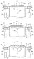
도 14는 상기와 상이한 익스팬딩 장치(60)를 이용하여 익스팬딩 테이프(13)를 확장하는 양태를 나타내고 있다. 즉, 이 익스팬딩 장치(60)로도 상기 제1 확장 단계나 제2 확장 단계를 행할 수 있다.Fig. 14 shows an embodiment in which the expanding
이 경우의 익스팬딩 장치(60)는 원통형의 테이블(61)의 주위에, 실린더 장치(62)에 의해 승강 가능한 승강 테이블(63)이 배치된 구성으로 되어 있고, 웨이퍼(1)는, 접착 시트(12)를 개재하여 웨이퍼(1)가 점착된 익스팬딩 테이프(13)에 상기 환형 프레임(14)이 미리 점착된 상태로 세팅된다. 테이블(61)의 내부에는, 익스팬딩 테이프(13)를 향하여 냉각 유체를 분출하는 노즐(64)이 배치되어 있다.The
웨이퍼(1)의 확장은, 우선, 도 14의 (a)에 나타내는 바와 같이, 승강 테이블(63)의 높이 위치를 테이블(61)과 동일하게 하여, 테이블(61)의 상단면에 익스팬딩 테이프(13) 상의 웨이퍼(1)를 배치하고, 승강 테이블(63) 상에 환형 프레임(14)을 배치한다. 계속해서, 승강 테이블(63)에 설치된 클램프(65)로 환형 프레임(14)을 승강 테이블(63)에 고정한다.14 (a), the elevation position of the elevation table 63 is set to be the same as that of the table 61, The
그리고, 도 14의 (b)에 나타내는 바와 같이 노즐(64)로부터 냉각 유체를 분출시킴으로써 접착 시트(12)를 냉각한 상태로, 실린더 장치(62)를 축소시켜, 접착 시트(12)의 과잉부(12a)를 분단하는 제1 확장 단계를 행한다. 승강 테이블(63)이 하강하면, 익스팬딩 테이프(13)는 외측으로 확장되어, 접착 시트(12)의 과잉부(12a)가 분단된다.14 (b), the
계속해서, 웨이퍼(1)의 표면으로부터 보호 부재(11)를 제거하고 나서, 도 14의 (c)에 나타내는 바와 같이 승강 테이블(63)을 더 하강시켜 익스팬딩 테이프(13)를 확장하고, 웨이퍼(1)를 칩(3)으로 분할하는 제2 확장 단계를 행한다.14 (c), the lifting table 63 is further lowered to expand the expanding
이와 같이 익스팬딩 장치(60)에 의해서도 제1 확장 단계 및 제2 확장 단계를 행할 수 있다. 제1 확장 단계에 있어서는 웨이퍼(1)의 표면(1a)에 보호 부재(11)가 점착되어 있기 때문에, 제1 확장 단계에서 생기는 접착 시트(12)의 과잉부(12a)의 파단 부스러기(12b)가 웨이퍼(1)의 표면(1a)에 부착되는 일은 없다.As described above, the expanding
또한, 상기 실시형태에서는, 웨이퍼(1)의 분할 예정 라인을 따라 형성하는 분할 기점을, 레이저 빔 조사에 의한 개질층(1c)으로 구성하고 있지만, 분할 기점은, 예컨대 웨이퍼(1)의 표면(1a)측에 형성하는 홈이어도 좋고, 그 홈은, 절삭 블레이드로 형성한 절삭홈이나, 웨이퍼(1)에 대하여 흡수성을 갖는 파장의 레이저 빔을 조사하여 형성하는 레이저 가공홈 등을 들 수 있다.In the above embodiment, the division originating points formed along the line along which the wafer is divided on the
또한, 웨이퍼(1)의 이면 연삭과 분할 기점을 형성하는 순서는 임의이며, 상기 실시형태와는 반대로, 분할 기점을 형성하고 나서 웨이퍼(1)의 이면 연삭을 행하여도 좋다.The back grinding of the
1: 웨이퍼(판형물)1a: 웨이퍼의 표면
1c: 개질층(분할 기점)3: 칩
11: 보호 부재12: 접착 시트
12a: 접착 시트의 과잉부13: 익스팬딩 테이프
14: 환형 프레임14a: 환형 프레임의 개구1: wafer (plate) 1a: surface of wafer
1c: reforming layer (division starting point) 3: chip
11: protective member 12: adhesive sheet
12a: excess portion of the adhesive sheet 13: expansive tape
14:
Claims (2)
Translated fromKorean판형물보다 대직경의 접착 시트를 개재하여 판형물을 익스팬딩 테이프 상에 배치하는 점착 단계와,
상기 점착 단계를 실시한 후, 판형물의 표면에 상기 보호 부재가 배치된 상태로 상기 익스팬딩 테이프를 확장하여 판형물의 외주측으로 비어져 나온 상기 접착 시트를 분단하는 제1 확장 단계와,
상기 제1 확장 단계를 실시한 후, 판형물의 표면에 배치된 상기 보호 부재를 제거하는 보호 부재 제거 단계와,
상기 보호 부재 제거 단계를 실시한 후, 상기 익스팬딩 테이프를 확장하여 판형물을 상기 분할 기점으로부터 상기 분할 예정 라인을 따라 분할하며 판형물에 대응하는 상기 접착 시트를 상기 분할 예정 라인을 따라 파단하는 제2 확장 단계
를 포함하는 것을 특징으로 하는 가공 방법.A method of processing a plate-like object having a protective member disposed on a surface thereof and having a dividing base point along a line to be divided,
Comprising the steps of: placing a plate-shaped article on an expanding tape via an adhesive sheet having a larger diameter than a plate-shaped article;
A first expanding step of expanding the expanding tape in a state in which the protective member is disposed on the surface of the plate-like object after the adhesion step, thereby separating the adhesive sheet that has been discharged to the outer periphery side of the plate-
A protective member removing step of removing the protective member disposed on the surface of the plate-like object after the first expansion step;
Dividing the plate-shaped object from the dividing base point along the dividing line, expanding the expanding tape after performing the protecting member removing step, and cutting the adhesive sheet corresponding to the plate- Expansion phase
And a machining method.
Applications Claiming Priority (2)
| Application Number | Priority Date | Filing Date | Title |
|---|---|---|---|
| JPJP-P-2012-206913 | 2012-09-20 | ||
| JP2012206913AJP5977633B2 (en) | 2012-09-20 | 2012-09-20 | Processing method |
Publications (2)
| Publication Number | Publication Date |
|---|---|
| KR20140038305Atrue KR20140038305A (en) | 2014-03-28 |
| KR101966997B1 KR101966997B1 (en) | 2019-04-08 |
Family
ID=50318630
Family Applications (1)
| Application Number | Title | Priority Date | Filing Date |
|---|---|---|---|
| KR1020130105964AActiveKR101966997B1 (en) | 2012-09-20 | 2013-09-04 | Machining method |
Country Status (3)
| Country | Link |
|---|---|
| JP (1) | JP5977633B2 (en) |
| KR (1) | KR101966997B1 (en) |
| CN (1) | CN103681492B (en) |
Families Citing this family (6)
| Publication number | Priority date | Publication date | Assignee | Title |
|---|---|---|---|---|
| JP6494360B2 (en)* | 2015-03-25 | 2019-04-03 | 株式会社ディスコ | Expansion unit |
| JP6671794B2 (en)* | 2016-05-11 | 2020-03-25 | 株式会社ディスコ | Wafer processing method |
| JP6710457B2 (en)* | 2016-06-01 | 2020-06-17 | 株式会社ディスコ | Expanded sheet, method for manufacturing expanded sheet, and method for expanding expanded sheet |
| JP7216504B2 (en)* | 2018-09-03 | 2023-02-01 | 株式会社ディスコ | Expanding method |
| JP7345328B2 (en) | 2019-09-13 | 2023-09-15 | 株式会社ディスコ | Processing method of workpiece |
| JP7511981B2 (en)* | 2020-08-05 | 2024-07-08 | 株式会社ディスコ | Method for manufacturing chip with adhesive film |
Citations (5)
| Publication number | Priority date | Publication date | Assignee | Title |
|---|---|---|---|---|
| KR20060093036A (en)* | 2005-02-18 | 2006-08-23 | 가부시기가이샤 디스코 | Wafer splitting method |
| KR20090089340A (en)* | 2007-02-27 | 2009-08-21 | 인터내셔널 비지네스 머신즈 코포레이션 | Rectifier for Crosspoints Based on Memory Array Architecture |
| JP2009272503A (en) | 2008-05-09 | 2009-11-19 | Disco Abrasive Syst Ltd | Breaking device and breaking method for filmy adhesive |
| KR20100052080A (en)* | 2008-11-10 | 2010-05-19 | 주식회사 하이닉스반도체 | Resistive memory device and method for manufacturing the same |
| JP2011129606A (en)* | 2009-12-16 | 2011-06-30 | Furukawa Electric Co Ltd:The | Method of processing semiconductor wafer |
Family Cites Families (6)
| Publication number | Priority date | Publication date | Assignee | Title |
|---|---|---|---|---|
| JPS6134955A (en)* | 1984-07-26 | 1986-02-19 | Teikoku Seiki Kk | Automatic separation of silicon wafer |
| JPS6155940A (en)* | 1984-08-27 | 1986-03-20 | Nec Corp | Pelletizing device of semiconductor wafer |
| JP2004273895A (en)* | 2003-03-11 | 2004-09-30 | Disco Abrasive Syst Ltd | Method of dividing semiconductor wafer |
| JP4478053B2 (en)* | 2005-03-29 | 2010-06-09 | 株式会社ディスコ | Semiconductor wafer processing method |
| JP4971869B2 (en)* | 2007-05-11 | 2012-07-11 | 株式会社ディスコ | Adhesive film breaker |
| JP5133660B2 (en)* | 2007-11-27 | 2013-01-30 | 株式会社ディスコ | Breaking method of adhesive film mounted on backside of wafer |
- 2012
- 2012-09-20JPJP2012206913Apatent/JP5977633B2/enactiveActive
- 2013
- 2013-09-04KRKR1020130105964Apatent/KR101966997B1/enactiveActive
- 2013-09-12CNCN201310414816.4Apatent/CN103681492B/enactiveActive
Patent Citations (5)
| Publication number | Priority date | Publication date | Assignee | Title |
|---|---|---|---|---|
| KR20060093036A (en)* | 2005-02-18 | 2006-08-23 | 가부시기가이샤 디스코 | Wafer splitting method |
| KR20090089340A (en)* | 2007-02-27 | 2009-08-21 | 인터내셔널 비지네스 머신즈 코포레이션 | Rectifier for Crosspoints Based on Memory Array Architecture |
| JP2009272503A (en) | 2008-05-09 | 2009-11-19 | Disco Abrasive Syst Ltd | Breaking device and breaking method for filmy adhesive |
| KR20100052080A (en)* | 2008-11-10 | 2010-05-19 | 주식회사 하이닉스반도체 | Resistive memory device and method for manufacturing the same |
| JP2011129606A (en)* | 2009-12-16 | 2011-06-30 | Furukawa Electric Co Ltd:The | Method of processing semiconductor wafer |
Also Published As
| Publication number | Publication date |
|---|---|
| JP5977633B2 (en) | 2016-08-24 |
| CN103681492A (en) | 2014-03-26 |
| JP2014063812A (en) | 2014-04-10 |
| CN103681492B (en) | 2018-02-16 |
| KR101966997B1 (en) | 2019-04-08 |
Similar Documents
| Publication | Publication Date | Title |
|---|---|---|
| KR101990650B1 (en) | Machining method | |
| KR20140038303A (en) | Machining method | |
| KR101966997B1 (en) | Machining method | |
| US8486806B2 (en) | Method for machining wafers by cutting partway through a peripheral surplus region to form break starting points | |
| US9905453B2 (en) | Protective sheeting for use in processing a semiconductor-sized wafer and semiconductor-sized wafer processing method | |
| JP4767122B2 (en) | Method for replacing tape and method for dividing substrate using the method for replacing tape | |
| TWI459452B (en) | A method of breaking the film attached to the back of the wafer, and a subsequent film | |
| TW201742131A (en) | Wafer processing method | |
| KR102023203B1 (en) | Machining method | |
| CN108987268A (en) | The processing method of chip | |
| JP5879698B2 (en) | Semiconductor substrate expansion apparatus and expansion processing method | |
| JP6009240B2 (en) | Wafer processing method | |
| JP2005109155A (en) | Semiconductor wafer processing method | |
| JP6298699B2 (en) | Wafer processing method | |
| JP2011124260A (en) | Wafer processing method | |
| JP2013041908A (en) | Method of dividing optical device wafer | |
| JP6537414B2 (en) | Wafer processing method | |
| JP6045426B2 (en) | Wafer transfer method and surface protection member | |
| JP6751337B2 (en) | Method of breaking adhesive film | |
| JP6137999B2 (en) | Wafer processing method | |
| JP2023097472A (en) | Expanding device and expanding method | |
| JP5545624B2 (en) | Wafer processing method | |
| CN117581351A (en) | A method and system for manufacturing semiconductor products | |
| JP2021158164A (en) | Device chip manufacturing method |
Legal Events
| Date | Code | Title | Description |
|---|---|---|---|
| PA0109 | Patent application | Patent event code:PA01091R01D Comment text:Patent Application Patent event date:20130904 | |
| PG1501 | Laying open of application | ||
| A201 | Request for examination | ||
| PA0201 | Request for examination | Patent event code:PA02012R01D Patent event date:20170904 Comment text:Request for Examination of Application Patent event code:PA02011R01I Patent event date:20130904 Comment text:Patent Application | |
| E902 | Notification of reason for refusal | ||
| PE0902 | Notice of grounds for rejection | Comment text:Notification of reason for refusal Patent event date:20180924 Patent event code:PE09021S01D | |
| E701 | Decision to grant or registration of patent right | ||
| PE0701 | Decision of registration | Patent event code:PE07011S01D Comment text:Decision to Grant Registration Patent event date:20190103 | |
| GRNT | Written decision to grant | ||
| PR0701 | Registration of establishment | Comment text:Registration of Establishment Patent event date:20190402 Patent event code:PR07011E01D | |
| PR1002 | Payment of registration fee | Payment date:20190402 End annual number:3 Start annual number:1 | |
| PG1601 | Publication of registration | ||
| PR1001 | Payment of annual fee | Payment date:20220323 Start annual number:4 End annual number:4 | |
| PR1001 | Payment of annual fee | Payment date:20230306 Start annual number:5 End annual number:5 | |
| PR1001 | Payment of annual fee | Payment date:20240320 Start annual number:6 End annual number:6 | |
| PR1001 | Payment of annual fee | Payment date:20250318 Start annual number:7 End annual number:7 |