KR20140030215A - Direct drive waveform generator - Google Patents
Direct drive waveform generatorDownload PDFInfo
- Publication number
- KR20140030215A KR20140030215AKR1020137031239AKR20137031239AKR20140030215AKR 20140030215 AKR20140030215 AKR 20140030215AKR 1020137031239 AKR1020137031239 AKR 1020137031239AKR 20137031239 AKR20137031239 AKR 20137031239AKR 20140030215 AKR20140030215 AKR 20140030215A
- Authority
- KR
- South Korea
- Prior art keywords
- input
- output
- controlled oscillator
- voltage controlled
- coupled
- Prior art date
- Legal status (The legal status is an assumption and is not a legal conclusion. Google has not performed a legal analysis and makes no representation as to the accuracy of the status listed.)
- Granted
Links
Images


Classifications
- H—ELECTRICITY
- H03—ELECTRONIC CIRCUITRY
- H03K—PULSE TECHNIQUE
- H03K7/00—Modulating pulses with a continuously-variable modulating signal
- H03K7/08—Duration or width modulation ; Duty cycle modulation
- H—ELECTRICITY
- H10—SEMICONDUCTOR DEVICES; ELECTRIC SOLID-STATE DEVICES NOT OTHERWISE PROVIDED FOR
- H10N—ELECTRIC SOLID-STATE DEVICES NOT OTHERWISE PROVIDED FOR
- H10N30/00—Piezoelectric or electrostrictive devices
- H10N30/80—Constructional details
- H10N30/802—Circuitry or processes for operating piezoelectric or electrostrictive devices not otherwise provided for, e.g. drive circuits
Landscapes
- Dc-Dc Converters (AREA)
- General Electrical Machinery Utilizing Piezoelectricity, Electrostriction Or Magnetostriction (AREA)
Abstract
Translated fromKoreanDescription
Translated fromKorean본 발명은 전지 구동 드라이버에 관한 것으로, 특히, 저전압 제어 신호에 유사한 고전압 파형을 만들고, 압전 장치(piezoelectric device)에 직접적으로 파형을 인가(apply)하는 것에 의해 장치를 구동하는 압전 장치용 구동장치에 관한 것이다.BACKGROUND OF THE
압전 구동기(piezoelectric actuator)는 1.5 ~ 12.6V의 일반적인 전지 전압보다 큰 고전압이 요구된다. "고(high)" 전압은 현재 전형적인 구동 전압인 100 ~ 120V이 포함되는 20 ~ 200V 이다. 일부 액튜에이터용의 라인 구동 전원은 1000V 정도의 고전압을 제공한다. 전지로부터 고전압을 생성하는 것은 전력선으로부터 고전압을 생성하는 것보다 더 어렵다.Piezoelectric actuators require higher voltages than typical cell voltages of 1.5-12.6V. The "high" voltage is now 20 to 200V, which includes the typical drive voltage of 100 to 120V. Line drive power supplies for some actuators provide high voltages as high as 1000V. Generating high voltage from a cell is more difficult than generating high voltage from a power line.
전압 승압용 컨버터(voltage boost converter)는 전지로부터 구동장치(driver)를 위한 고전압으로 저전압을 변환하기 위하여 사용될 수 있다. 승압용 컨버터에서, 인덕터(inductor)에 저장된 에너지는 고전압의 전류 펄스들로서 캐패시터(capacitor)에 공급된다.Voltage boost converters can be used to convert low voltages from batteries to high voltages for drivers. In a boost converter, the energy stored in the inductor is supplied to the capacitor as high voltage current pulses.
도 1은 공지된 승압용 컨버터를 포함하는 회로도이다{미국특허 3,913,000 (Cardwell, Jr.) 및 미국특허 4,527,096(Kindlmann)을 예로 참조}. 인덕터(11) 및 트랜지스터(12)는 전원(13)과 접지(ground) 또는 공통접지(common) 사이에서 직렬로 연결된다. 트랜지스터(12)가 턴 온(turn on, conduct)될 때, 전류가 인덕터(11)를 통해 흐르면서, 인덕터(11)에 의해 형성된 자계에 에너지가 저장된다. 배터리 전압, 인덕턴스(inductance), 내부 저항(internal resistance), 그리고 트랜지스터(12)의 온-저항(on-resistance)에 따라 인덕터(11)를 통해 흐르는 전류는 급속히 증가한다. 트랜지스터(12)가 차단되면, 자계(magnetic field)는 트랜지스터(12)의 턴-오프(turn-off) 특성에 의해 결정되는 비율(rate)로 감소한다. 감소비율(rate of collapse)은 매우 빠르며, 자계가 증가하는 비율보다도 훨씬 빠르다. 인덕터(11)의 양단 전압은 자계가 감소하는 비율에 비례한다. 100 V 또는 그 이상의 전압도 가능하다. 따라서, 저전압은 승압 컨버터(boost converter)에 의해 고전압으로 변환된다.1 is a circuit diagram including a known boost converter (see, for example, US Patent 3,913,000 (Cardwell, Jr.) and US Patent 4,527,096 (Kindlmann)).
트랜지스터(12)가 차단(shut-off)되면, 접합부(15)의 전압은 기본적으로 캐패시터(capacitor ; 14)의 전압보다 더 높고, 전류는 순방향으로 바이어스된 다이오드(16)을 통해 흐른다. 전류의 각 펄스는 캐패시터(14)를 조금씩 충전시키고, 캐패시터의 전하는 점진적으로 증가한다. 특정 시점에서, 캐패시터(14)의 전압은 전원 전압보다 크게 된다. 다이오드(16)는 캐패시터(14)로부터 전원(13)으로 전류가 흐르는 것을 방지한다. 캐패시터(14)의 전압은 증폭기(21)와 같은 다른 회로 소자들을 위한 공급전압이다.When
증폭기(21)의 출력은 압전 구동기(piezoelectric actuator ; 22)에 연결된다. 증폭기(21)의 입력은 양방향 구동용(bi-directional movement) 교류 신호 또는 단방향 구동용(unidirectional movement) 직렬 신호 또는 절반의 상보적인 구동(as half of a complementary drive)으로서 수신할 수 있다(각각의 극성마다 압전 구동기(22)의 반대 단자들에 연결된 2개의 증폭기들 ; two amplifiers, one for each polarity, coupled to opposite terminals of piezoelectric actuator 22). 상보적 구동(complementary drive)에서, 승압된 전압의 절대값은 전지전압의 절대값보다 크다. 상보적 구동(complementary drive)은 단일 구동의 고전압 절반을 이용할 수(또는 고전압의 2배로 제공될 수) 있으나, 2개의 승압 컨버터들이 필요하다.The output of the
펄스폭 변조(PWM) 신호들로부터 저전압 파형을 생성하는 것은 공지기술로 알려져 있다{미국특허 4,914,396(Berthiaume), 5,703,473 (Phillips et al.) 및 5,994,973 (Toki) 참조}. 고전압을 취급하는 것은 고전압을 절연하고 제어해야 하는 장치들을 제조해야 하기 때문에 어렵고, 비용이 더 많이 든다. 고전압 증폭기는 효율을 더 감소시키는 손실들을 야기한다. 저장 커패시터는 귀중한 보드(board)의 공간을 차지하며, 도 1에 나타낸 드라이버(driver)의 회로도는 다른 응용 회로들에서 쉽게 적용되지 않는다.The generation of low voltage waveforms from pulse width modulated (PWM) signals is known in the art (see US Patent 4,914,396 (Berthiaume), 5,703,473 (Phillips et al.) And 5,994,973 (Toki)). Handling high voltages is difficult and more expensive because devices must be insulated and controlled for high voltages. High voltage amplifiers cause losses that further reduce efficiency. The storage capacitor occupies valuable board space, and the circuit diagram of the driver shown in FIG. 1 is not easily applied in other application circuits.
여기서 사용된 것으로서, 파형에서 "유사한" 은 정확한 복제(replica)를 의미하는 것이 아니라, 근사치에 가깝다는 것이다.As used herein, "similar" in the waveform does not mean an exact replica, but rather is an approximation.
상기의 관점에 따른 본 발명의 목적은 햅틱 드라이버(haptic driver)에서 저장 커패시터를 제거하는 것이다.The object of the present invention according to the above point is to remove the storage capacitor from the haptic driver.
본 발명의 또 다른 목적은 햅틱 드라이버에서 고전압 증폭기를 제거하는 것이다.Another object of the present invention is to eliminate the high voltage amplifier in the haptic driver.
본 발명의 또 다른 목적은 제어회로가 고전압 회로에 독립적인 낮은 전압의 소자들을 사용하는 드라이버를 제공하는 것이다.It is yet another object of the present invention to provide a driver in which the control circuit uses low voltage elements independent of the high voltage circuit.
발명의 또 다른 목적은 외부 소자들을 변경함에 의해 더 높은 전압과 전류를 지원하도록 쉽게 확장할 수 있는 드라이버를 제공하는 것이다.Another object of the invention is to provide a driver that can be easily extended to support higher voltages and currents by changing external components.
상기 목적들은 본 발명에서 낮은 전압 입력 파형에 유사한 높은 전압 파형을 생성하여 이루어 질 수 있다. 고전압 파형은 장치에 직접 인가되는(applied) 일련의 펄스들이다. 에러 신호는 주파수, 진폭 및 펄스들의 주기(duration of the pulses)를 제어한다. 고전압 파형으로부터 얻은 피드백 신호는 에러 신호를 생성하는 입력 파형과 비교된다.The above objects can be achieved by generating a high voltage waveform similar to the low voltage input waveform in the present invention. The high voltage waveform is a series of pulses applied directly to the device. The error signal controls the frequency, amplitude and duration of the pulses. The feedback signal obtained from the high voltage waveform is compared with the input waveform producing an error signal.
본 발명은 저장 캐패시터 및 종래 기술의 구동기들(drivers)에서 사용되는 고전압 증폭기를 제거한 직접 구동 파형 발생기(direct drive waveform generator)를 제공한다. 제어회로는 고전압 회로와 독립적인 낮은 전압의 부품들을 사용한다. 발생기는 쉽게 외부 부품들을 변경하여 더 높은 전압과 전류를 지원하도록 확장될 수 있다.The present invention provides a direct drive waveform generator that eliminates the high voltage amplifier used in storage capacitors and prior art drivers. The control circuit uses low voltage components that are independent of the high voltage circuit. The generator can be easily extended to support higher voltages and currents by changing external components.
본 발명의 보다 완전한 이해는 첨부된 도면과 함께 다음의 상세한 설명을 통하여 얻을 수 있다.
도 1은 종래 기술에 따라 구성되는 압전 구동기에 연결된 드라이버(driver)의 회로도이다.
도 2는 디스플레이와 키패드 중 한쪽 또는 양쪽에 압전 구동기를 포함하는 디스플레이와 키패드를 갖는 전자 장치의 사시도이다.
도 3은 본 발명에 따라 구성된 압전 구동기에 연결되는 드라이버의 회로도이다.
도 4는 도 3에 도시된 드라이버를 위한 제어회로의 블록도이다.
도 5는 본 발명에 따라 구성된 드라이버를 위한 디지털 제어회로의 블록도이다.
도 6은 본 발명에 따라 구성된 파형 발생기의 동작을 도시한 그래프이다.
도 7은 본 발명에 따라 구성된 드라이버를 위한 아나로그(analog) 제어회로의 블록도이다.
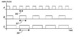
도 8은 듀티 사이클(duty cycle), 온-타임(on-time) 및 주파수 간의 관계를 도시한 도면이다.
도 9는 본 발명에 따라 구성된 파형 발생기의 동작을 도시한 도면이다.
도 10은 생성되는 파형을 상세히 도시한 도면이다.
도 11은 본 발명의 다른 실시예에 따른 블록도이다.
도 12는 본 발명에 따라 구성된 시스템의 상태도이다.
도 13은 복수의 상태들에서 발생되는 변화 방법을 보여주는 표이다.A more complete understanding of the invention may be obtained through the following detailed description in conjunction with the accompanying drawings.
1 is a circuit diagram of a driver connected to a piezoelectric driver constructed according to the prior art.
2 is a perspective view of an electronic device having a display and a keypad including a piezoelectric driver on one or both of the display and the keypad.
3 is a circuit diagram of a driver connected to a piezoelectric driver constructed in accordance with the present invention.
4 is a block diagram of a control circuit for the driver shown in FIG.
5 is a block diagram of a digital control circuit for a driver constructed in accordance with the present invention.
6 is a graph illustrating the operation of a waveform generator constructed in accordance with the present invention.
7 is a block diagram of an analog control circuit for a driver constructed in accordance with the present invention.
FIG. 8 illustrates the relationship between duty cycle, on-time and frequency.
9 illustrates the operation of a waveform generator constructed in accordance with the present invention.
10 is a view showing in detail the generated waveform.
11 is a block diagram according to another embodiment of the present invention.
12 is a state diagram of a system constructed in accordance with the present invention.
13 is a table showing a change method occurring in a plurality of states.
도 2는 디스플레이(display ; 26)와 키패드(keypad ; 27)를 포함하는 전자장치(25)를 나타낸다. 디스플레이(26)나 키패드(27) 또는 양자 모두는 키(key) 또는 디스플레이의 일부가 약간 눌려질 때, 촉각에 의한 피드백을 제공하기 위한 (미도시) 압전 장치가 제공될 수 있다. 피드백을 제공하기 위한 장치는 해당 기술 분야에서 공지되어 있다. 앞에서 설명한 바와 같이, 그와 같은 장치는 단층 또는 복수의 층들을 가질 수 있으며, 양방향 또는 단방향일 수 있다.2 shows an
도 3은 도 1에 도시된 저장 캐패시터(14)와 고전압 증폭기(21)가 생략된 본 발명에 따른 적절한 실시예의 블럭도이다. 인덕터(31) 및 트랜지스터(32)는 전원(33)과 접지(ground) 또는 공통접지(common) 사이에서 직렬로 연결된다. 트랜지스터(32)의 제어단자는 충전입력(charge ; 35)에 연결된다. 인덕터(31)과 트랜지스터(32)의 접합 단자는 다이오드(36)에 의해 출력 단자(38)로 연결된다. 압전 구동기(22)는 출력 단자(38)과 접지 사이에 연결된다. 상기에서 설명한 회로는 압전 구동기(22)에 펄스들을 인가하기 위한 충전 회로이다. 주파수, 진폭 및 펄스의 주기는 충전 입력(35)에 인가되는 신호에 의해 결정된다.3 is a block diagram of a suitable embodiment according to the present invention with the
트랜지스터(41) 및 저항(42)은 출력 단자(38)와 접지 사이에 직렬로 연결된다. 트랜지스터(41)의 제어 단자는 방전입력(discharge ; 43)에 연결된다. 트랜지스터(41) 및 저항(42)은 압전 구동기에 축적된 전하를 방전하고, 더 나아가 장치에 인가된 파형에 기여(contribute)한다.
저항(47)과 저항(48)은 출력 단자(38)와 접지 사이에 직렬로 연결된다. 저항(47)과 저항(48)의 접합 부분은 피드백 출력(feedback ; 49)에 연결된다. 저항들은 출력 단자(38)와 접지 사이의 전압 비율을 피드백 출력(49)으로 제공하는 전압 분배기이다. 여기서, 감쇠계수로 언급되는 상기 전압 비율, ε는 다음과 같은 수학식과 같다.

피드백 신호는 충전 및 방전입력에 인가되는 신호들과 이에 따라 압전 구동기(22)에 인가되는 전압의 파형을 생성하는 데 사용된다. 파형은 원하는 모양, 예를 들어, 연속(정현파) 또는 불연속 형태{램프(ramp) 또는 펄스(pulse)})를 가질 수 있다.The feedback signal is used to generate a waveform of the signals applied to the charge and discharge inputs and thus the voltage applied to the
출력 "파형"은 출력 단자(38)에 인가되는 신호의 포락선(envelope)을 말한다(도 6 참조). 포락선은 다양한 진폭(magnitude)과 펄스폭(width)의 고주파 펄스의 일련의 결과이다. 압전 장치는 용량성(capacitive)이기 때문에, 약간 평활화(smoothing)가 발생하여 파형은 펄스들을 포함하지 않았던 것처럼 간주될 수 있다.The output "waveform" refers to the envelope of the signal applied to the output terminal 38 (see Figure 6). The envelope is the result of a series of high frequency pulses of varying magnitude and pulse width. Since piezoelectric devices are capacitive, some smoothing may occur and the waveform may be considered as if it did not contain pulses.
도 4는 도 3에 도시된 드라이버의 제어회로에 대한 블록도이다. 제어회로(control ; 51)는 아나로그 또는 디지털일 수 있고, 도 3에 도시된 바와 같이, 피드백 출력(49)에 연결되는 피드백 입력(feedback ; 52) 및 파형 입력(waveform ; 53)을 포함한다. 파형 입력(53)은 도 1에 도시된 앰프(21)의 입력에 해당한다. 제어회로(51)는 도 3에 도시된 충전입력(35)에 연결되는 충전출력(55)과 방전입력(43)에 연결되는 방전출력(56)을 포함한다. 제어회로(51)가 디지털인 경우, 제어회로(51)가 복제하려는 입력 또는 레퍼런스(reference)는 아나로그 신호, 시간과 전압값의 표(table) 또는 기준값(reference value)이 될 수 있다.4 is a block diagram of the control circuit of the driver shown in FIG. The
도 5와 도 6에서, 플러스(+)와 마이너스(-) 기호를 가진 삼각형은 비교기이며, 출력은 디지털(0 또는 1)이다. 플러스(+)와 마이너스(-) 기호를 갖지 않는 삼각형은 차동 증폭기이며, 출력은 아나로그이다.In Figures 5 and 6, triangles with plus and minus signs are comparators and the output is digital (0 or 1). Triangles with no plus and minus signs are differential amplifiers and the output is analog.
도 5에서 마이크로 컨트롤러(micro controller ; 61)는 아나로그 / 디지탈 컨버터(ADC ; 63)에 의해 피드백 입력(62)에 연결된다. 마이크로 컨트롤러(61)의 입력(64)은 마이크로 컨트롤러(61)에서 요구되는 파형을 묘사하는(describing) 정보를 연결한다. 상기 정보는 아나로그 또는 디지털일 수 있고 상기 파형 그 자체를 나타낼 수 있고, 또한, 마이크로 컨트롤러(61)에 미리 프로그램된 파형 중에서 선택하기 위한 데이터일 수 있다. 파형을 묘사하는 디지털 데이터는 디지털 신호로서 비교기(67)에서 피드백 신호와 비교되는 레퍼런스 신호를 생성하기 위하여, 디지털/ 아나로그 컨버터(DAC ; 66)에서 변환된다. 비교기(67)는 더 큰 신호가 어느 신호인지 및 충전회로나 방전회로 중 어느 하나가 작동하는지에 대한 표시(indication)를 제공한다.In FIG. 5 a
펄스폭 변조기(PWM ; 71)는 출력(72)에 연결되며, 충전출력(73)과 방전출력(74)에 연결된 상보적인 출력들(complementary outputs)을 갖는다. 선택적으로 로우 패스 필터(Low Pass Filter, LPF ; 75)는 펄스 폭 변조기(71) 및 방전출력(74) 사이에 연결될 수 있다. 로우 패스 필터(75)는 펄스를 평균화(average)하고, 방전 속도를 느리게 한다.Pulse width modulator (PWM) 71 is coupled to
마이크로 컨트롤러(61)는 다중 상태, 유한 상태 기기(multi-state, finite state machine)이다. 마이크로 컨트롤러(61)는 충전과 방전, 두 개의 기본 모드를 가진다. 정확성을 개선하기 위해, 여러 하위 상태(sub-states)는 충전 사이클과 방전 사이클 모두에 사용된다. 압전 장치는 그것이 충전될 수 있는 것보다 더 빨리 방전될 수 있으며, 이것은 기계 상태(machine state)에서 제공된다. 기계 상태를 설명하는 의사 코드( Pseudo-code)는 본 명세서 끝부분의 추록(Appendix)에 있다.The
비교기(67)는 피드백 상태 변화에 대한 신속한 응답을 제공하고, 에러의 한 비트 양자화를 수행한다. 에러, δ, 는 피드백 신호값과 기준 신호값의 차이로 정의된다. 이러한 차이는 ADC(63)의 출력과 DAC(66)의 입력으로부터 마이크로 컨트롤러(61)에서 계산된다. 에러가 이러한 방식으로 정의될 때, 충전 회로의 이상적인 이득은 이전에 정의된 피드백 감쇠 계수, ε의 역수이다. 비교기(67)는 ADC(63)의 샘플링 속도보다 10-100배 빠른 응답 시간을 가져야 한다. 비교기 변환(추록 참조)과 관련된 인터럽트 서비스 루틴은 다른 비교기 변환의 경우 이전 상태로 프로그램을 리턴하는 일시 정지 상태로서 제공하거나, 또는 디지털 샘플에 인접한 아나로그가 완료될 때, 다른 상태로 프로그램을 전송한다.
에러값은 유한 상태 기계(finite state machine)의 다음 상태를 결정한다. 네거티브 에러(negative error)는 컨트롤러가 부하를 충전하는 것을 의미하고, 포지티브 에러(positive error)는 컨트롤러가 부하를 방전하는 것을 의미한다. 충전과 방전, 에러 범위들에 해당하는 다양한 속도들(speeds)에 대한 여러 가지 상태들이 있다. 이러한 각 상태들에서 펄스 폭 변조기의 듀티 사이클(duty cycle)은 원활한 변환을 보장하기 위해 상태의 최대 듀티 사이클까지 적절하게 증가된다.The error value determines the next state of the finite state machine. Negative error means that the controller charges the load, and positive error means that the controller discharges the load. There are different states for various speeds that correspond to charge, discharge, and error ranges. In each of these states, the duty cycle of the pulse width modulator is appropriately increased up to the maximum duty cycle of the state to ensure smooth transitions.
부하를 충전하기 위해, 유도 충전 펌프(inductive charge pump)는 입력 신호가 이득 계수(gain factor)와 곱해지고 부하에 따라가는 것과 같은 방식으로 전환된다(To charge the load, the inductive charge pump is switched in such a fashion that the input signal is multiplied by a gain factor and mimicked on the load.). 인덕터의 최대 포화점에서, 인덕터에 저장되는 에너지는 도 3에 도시된 트랜지스터(32)가 도전되는(conductive) 시간의 길이에 따라 달라진다. 트랜지스터(32)가 턴 오프(turn off)될 때. 출력 전압은 자기장이 인덕터를 통해 감소하는 속도에 비례한다. 인덕터에 저장된 에너지가 많을수록, 출력 전압이 높다. 따라서, 온-타임(on-time)이 이득을 제어한다. 일련의 온-타임에 변화되는 펄스들은 입력 신호를 따라가는 포락선을 갖는다.To charge the load, an inductive charge pump is switched in the same way that the input signal is multiplied by a gain factor and follows the load. a fashion that the input signal is multiplied by a gain factor and mimicked on the load.). At the maximum saturation point of the inductor, the energy stored in the inductor depends on the length of time the
출력 신호의 최대 정확도를 얻기 위하여, 유도 충전 펌프(inductive charge pump)의 스위칭 주파수는 적어도 1000배, 바람직하게 수천배의 부하에 요구되는 출력 신호의 나이퀴스트(Nyquist) 주파수이다. 본 발명에 따른 한 실시예에서, 300 Hz의 주파수를 갖는 출력 신호는 150 kHz의 충전 주파수로 생성된다.In order to obtain the maximum accuracy of the output signal, the switching frequency of the inductive charge pump is the Nyquist frequency of the output signal required for at least 1000 times, preferably thousands of times the load. In one embodiment according to the invention, an output signal having a frequency of 300 Hz is generated with a charging frequency of 150 kHz.
신호가 32 kHz에서 샘플링 되면, 상기 16 kHz(나이퀴스트 주파수) 초과 신호의 주파수성분은 신호가 디지털/아나로그 변환기에 의해 재생성될 때, 앨리어싱(aliasing)을 야기할 것이다. 나이퀴스트 주파수는 정확도(fidelity)에 대한 최소 임계값이다. 순수한 톤(pure tone)은 고조파를 갖지 않는다. 구형파들(square waves)에는 홀수 고조파들(odd harmonics)이 풍부하다. 만약 원하는 출력신호가 구형파인 경우, 나이퀴스트 주파수는 동일한 주파수의 순수한 톤(tone)보다 더 높다. 도 6에서, 파형 A는 입력 파형이며, 파형 B는 도 3에 도시된 단자(38)에서의 출력 파형이다. 24개의 펄스들은 각 주기의 포락선(78)을 생성한다.If the signal is sampled at 32 kHz, the frequency component of the signal above 16 kHz (Nyquist frequency) will cause aliasing when the signal is regenerated by the digital / analog converter. Nyquist frequency is the minimum threshold for fidelity. Pure tones have no harmonics. Square waves are rich in odd harmonics. If the desired output signal is a square wave, the Nyquist frequency is higher than the pure tone of the same frequency. In FIG. 6, waveform A is an input waveform, and waveform B is an output waveform at the terminal 38 shown in FIG. Twenty four pulses create an
마이크로 컨트롤러(61) 내의 연산 장치는 현대적 마이크로 컨트롤러의 능력의 범위 내에서 적절하게, 펄스 폭 변조기(71)로부터의 신호의 한 주기 내에서 모든 제어의 연산들을 할 수 있어야 한다.The computing device in the
도 7에서 제어회로(80)는 비교기(83)에 연결된 피드백 입력(feedback ; 81)과 파형 입력(waveform ; 82)을 포함한다. 비교기(83)의 출력은 AND 게이트(86)의 한쪽 입력과 인버터(84)로 연결된다. 인버터(84)의 출력은 AND 게이트(86)의 한쪽 입력에 연결된다. 인버터(84)가 동시에 동작하는 것을 방지하는동안, 비교기(83)는 충전회로(charge)가 동작할지, 방전회로(discharge)가 동작할지 여부를 결정한다. 만약 피드백 신호가 파형 신호보다 크다면, 방전회로가 동작된다. 만약 피드백 신호가 파형 신호보다 작다면, 충전회로가 동작된다.In FIG. 7, the
피드백 입력(81) 및 파형입력(82)은 또한 편차 또는 에러 신호를 생성하는 차동증폭기(93)에 연결된다. 차동증폭기(93)의 출력은 전압 제어 오실레이터(VCO ; 92)의 주파수 제어 입력과 인버터(94)에 연결된다. 인버터(94)의 출력은 전압 제어 오실레이터(VCO ; 91)의 주파수 제어 입력과 전압 제어 오실레이터(92)의 듀티 사이클(duty cycle) 제어 입력에 연결된다. 전압 제어 오실레이터(91)로부터의 출력펄스들은 AND 회로(85)에 연결된다. 전압 제어 오실레이터(92)로부터의 출력펄스들은 AND 회로(86)에 연결된다.
도 8은 듀티 사이클, 온-타임(on-time) 및 주파수 간의 관계를 도시한다. 신호 A에 있어서, 펄스들은 소정의 주파수와 50%의 듀티 사이클을 갖는다. 온-타임(96)은 비교적 짧다. 신호 B에 있어서, 펄스들은 신호 A의 절반의 주파수와 50%의 듀티 사이클을 갖는다. 온-타임(97)은 온-타임(96)의 2배의 길이이다. 신호 C에 있어서, 펄스들은 신호 B와 동일 주파수를 갖지만, 75%의 듀티 사이클을 갖는다. 온-타임(98)은 온-타임(96)의 3배 길이이다.8 shows the relationship between duty cycle, on-time and frequency. For signal A, the pulses have a predetermined frequency and a duty cycle of 50%. On-
온-타임은 충전회로의 이득(gain)을 결정하기 때문에, 주파수 및 듀티 사이클은 정현파에서 피크들(peaks)을 생성하기 위한 충분한 이득을 확보하기 위하여 변화된다. 또한, 차동증폭기(93)의 출력인 오차(편차)신호의 진폭이 클 때 이득은 증가한다. 구체적으로 듀티 사이클은 큰 오차에서 증가하고 주파수는 큰 오차에서 감소한다. 반대쪽 센스(opposite sense)의 변화는 인버터(94)에 의해 제공된다.Since on-time determines the gain of the charging circuit, the frequency and duty cycle are varied to ensure sufficient gain to produce peaks in the sinusoidal wave. In addition, the gain increases when the amplitude of the error (deviation) signal, which is the output of the
도 9는 본 발명에 따라 구성된 파형 발생기의 동작을 도시한다. 충전 사이클 동안, 바람직하게는 주파수 및 듀티 사이클은 도 7에 도시된 차동증폭기(93)로부터의 오차 신호에 따라 변화된다. 방전 사이클 동안, 주파수는 부하가 방전됨에 따라 증가한다.9 illustrates the operation of a waveform generator constructed in accordance with the present invention. During the charge cycle, the frequency and duty cycle are preferably varied in accordance with the error signal from the
아나로그 제어회로의 장점은 더욱 정확한 제어를 제공하고 더 높은 주파수 파형에 가깝게 일치할 수 있다는 것이다. 아나로그 제어회로의 단점은 더욱 많은 튜닝을 요하며 쉽게 수정되기 어렵다는 것이다.The advantage of analog control circuitry is that it provides more accurate control and can closely match higher frequency waveforms. The disadvantage of analog control circuitry is that it requires more tuning and is not easily modified.
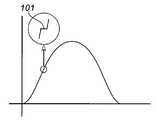
도 10은 생성된 파형을 도시한다. 확대된 영역(101)은, 파형에서 충전되는 회로로부터 비연속 전류 펄스들(discrete current pulses)에 의해 생기는 계단(step)을 도시한다. 이와 같은 계단들은 모든 응용들(applications)에 허용되거나 안 될 수 있다.10 shows the generated waveform. Magnified
도 11은 본 발명의 다른 실시예로서, 생성된 파형에서 계단들의 크기를 감소시킴으로써 생성된 파형에 보다 정확한 제어를 제공한 블록도이다. 파형 입력(waveform)은 요구되는 파형을 나타내는 아나로그 제어신호나 저장된 디지털 데이터일 수 있다. 도 11에 도시된 실시예에서, 파형 입력은 아나로그 컨버터(105)에서 디지털로부터 아나로그 신호로 변환되고 저역통과 필터(LPF ; 106)에서 평활되거나 평균화되어 저장되는 데이터이다. 저역통과 필터(106)의 출력은 비교기(108)의 반전된 입력(inverting input)에 연결된다. 피드백 입력(feedback ; 109)는 비교기(108)의 플러스 입력(positive input)에 연결된다.FIG. 11 is a block diagram of another embodiment of the present invention, which provides more accurate control of the generated waveform by reducing the magnitude of the steps in the generated waveform. The waveform input may be an analog control signal or stored digital data representing a desired waveform. In the embodiment shown in FIG. 11, the waveform input is data that is converted from digital to analog signal in
비교기(108)의 출력은 입력의 크기와 방향뿐만 아니라, 전환「예로서, 상태의 변화들(포지티브(positive)에서 네거티브(negative) 또는 네거티브에서 포지티브)」을 모니터링하는 마이크로 컨트롤러(110)의 A/D입력에 연결된다. 본 발명의 일 실시 예에서, 이것은 단지 2 비트의 정보를 요한다. 오차(error) 신호는 1로 표시되는 포지티브(positive) 또는 0(zero)로 표시되는 네가티브(negative) 중 하나이다. 진폭신호(magnitude signal)는 0으로 표시되는 로우(low) 또는 1로 표시되는 하이(high) 중 하나이다. 임의로 1 또는 0 중 하나가 지정된다.The output of the
도 7에 도시된 실시 예와 다소 유사하게, 피드백 신호(109)는 전압 제어 발진기의 주파수 입력 및 듀티 사이클 입력에 연결된다. 구체적으로, 피드백 신호(109)는 전압 제어 발진기(121)의 주파수 입력과 전압 제어 발진기(122)의 주파수 입력에 연결된다. 피드백 신호(109)는 전압 제어 발진기(121)의 듀티 사이클 입력에 인버터(124)를 통해 연결되고, 전압 제어 발진기(122)의 듀티 사이클 입력에 인버터(125)를 통해 연결된다. 전압 제어 발진기(121)의 출력은 AND 게이트(127)의 제1 입력에 연결된다. 전압 제어 발진기(122)의 출력은 AND 게이트(128)의 제1 입력에 연결된다. 마이크로 컨트롤러(110)의 x출력은 AND게이트(127)의 제2 입력에 연결된다. 마이크로 컨트롤러(110)의 y출력은 AND게이트(128)의 제2 입력에 연결된다. 출력 신호들은 표(131)에 표시된 바와 같이 AND 게이트들을 제어한다. 하나의 AND 게이트가 활성화(enable)될 수 있거나, 모든 AND 게이트가 불활성화될 수 있다. 둘 다 활성화되지 않을 경우, 시스템은 "일시 중지(pause)"상태이다.Somewhat similar to the embodiment shown in FIG. 7, the feedback signal 109 is coupled to the frequency input and duty cycle input of the voltage controlled oscillator. Specifically, the feedback signal 109 is connected to the frequency input of the voltage controlled
마이크로 컨트롤러(110)는 전압 제어 발진기(121)에 연결된 출력(133) 및 전압 제어 발진기(122)에 연결된 출력(134)을 포함한다. 출력(133) 및 출력(134)은 충전(또는 방전)을 빠르게 할지, 느리게 할지 여부를 조정하는 듀티 사이클을 정하는 전압 제어 발진기들의 한 쪽 입력을 선택할지, 또는 양쪽 입력을 선택할지 여부를 결정한다.The
도 12는 본 발명에 따라 구성된 시스템의 상태도이다. 도 13은 복수의 상태들 중 발생되는 전이 방법을 보여주는 표이다. 2개의 방전율(discharging rate)과 2개의 충전율(charging rate)의 조합에 의하여, 만약 요구되는 출력파형이 있다면, 매우 작은 단계들로 제공될 수 있다.12 is a state diagram of a system constructed in accordance with the present invention. 13 is a table illustrating a transition method occurring among a plurality of states. By the combination of two discharging rates and two charging rates, if there is an output waveform required, it can be provided in very small steps.
따라서, 본 발명은 저장 캐패시터 및 종래 기술의 구동기들(drivers)에서 사용되는 고전압 증폭기를 제거한 직접 구동 파형 발생기(direct drive waveform generator)를 제공한다. 제어회로는 고전압 회로와 독립적인 낮은 전압의 부품들을 사용한다. 발생기는 쉽게 외부 부품들을 변경하여 더 높은 전압과 전류를 지원하도록 확장될 수 있다.Accordingly, the present invention provides a direct drive waveform generator that eliminates the high voltage amplifier used in storage capacitors and prior art drivers. The control circuit uses low voltage components that are independent of the high voltage circuit. The generator can be easily extended to support higher voltages and currents by changing external components.
따라서 본 발명의 설명에서, 본 발명의 범위 내에서 할 수 있는 다양한 변형이 당업자에게 자명할 것이다. 예를 들어, 기능적으로, 트랜지스터(41) 및 저항(42)의 위치가 반대로 되어도 문제되지 않는다. 단일의 출력 단자와 함께 설명 및 도시하였지만, 본 발명은 용이하게 상보적(complementary) 또는 차동(differential) 출력으로 고전압 파형들을 제공하도록 조정된다. 듀티 사이클을 변화시키는 것은 어떤 응용들에서는 충전 제어로부터 생략될 수 있다. 외부 구성요소들(부품들)로서 도시되었을지라도, 많은 마이크로 컨트롤러들은 외부 구성요소들(부품들)로 이러한 구성요소들(부품들)에 대한 필요성을 배제하기 위해 복수의 ADC 및 DAC 회로들을 내장하여(on-board) 가질 수 있다. 응용에 따라서, 2개 이상의 충전 또는 방전레벨들이 증가하는 상태들의 수로 이용될 수 있다. 전하의 레벨들의 수는 고정되거나 프로그램 될 수 있다. 예를 들어, 마이크로 컨트롤러의 2개의 입력 핀들은, 본 발명에 따른 하나의 실시로부터 강화된 구동 유연성(drive flexibility)을 제공하고, 충전의 4개 레벨들 중 하나를 지정(address)할 수 있다.
Therefore, in the description of the present invention, various modifications that can be made within the scope of the present invention will be apparent to those skilled in the art. For example, functionally, it is not a problem even if the positions of the
11, 31 : 인덕터12, 32, 41 : 트랜지스터
13 : 전원14 : 캐퍼시터
15 : 접합부16, 36 : 다이오드
21, 93 : 증폭기
22 : 압전 구동기(piezoelectric actuator)
35 : 충전입력
38 : 출력단자42, 47, 48 : 저항
43 : 방전입력49 : 피드백(feedback) 출력
51, 80 : 제어회로52, 62, 81 : 피드백 입력
53, 82 : 파형입력55, 73 : 충전출력
56, 74 : 방전출력 61 : 마이크로 컨트롤러
63 : 아나로그 / 디지털 컨버터(ADC)
66 : 디지털 / 아나로그 컨버터(DAC)
67, 83 : 비교기71 : 펄스폭 변조기
75 : 로우 패스 필터(LPF)84 : 인버터
92 : 전압 제어 발진기11, 31:
13: power supply 14: capacitor
15:
21, 93: amplifier
22: piezoelectric actuator
35: charge input
38:
43: discharge input 49: feedback output
51, 80:
53, 82:
56, 74: discharge output 61: microcontroller
63: analogue / digital converter (ADC)
66: Digital / Analog Converter (DAC)
67, 83: comparator 71: pulse width modulator
75: low pass filter (LPF) 84: inverter
92: voltage controlled oscillator
Claims (15)
Translated fromKorean상기 출력 단자에 연결되며 방전 제어 입력을 갖는 방전 회로;
상기 출력 단자에 연결되는 피드백 회로; 및
상기 피드백 회로에 연결되는 입력, 파형 입력, 상기 충전 제어 입력에 연결되는 제1 출력; 및 상기 방전 제어 입력에 연결되는 제2 출력을 포함하는 제어회로를 포함하고,
상기 제어회로는 상기 파형 입력의 파형과 유사한 고전압 파형을 발생하기 위하여 상기 제1 출력 또는 상기 제2 출력 중 하나에 펄스 폭 변조 신호들을 생성하는 직접 구동 파형 발생기.An inductive boost circuit connected to the output terminal and having a charge control input;
A discharge circuit connected to said output terminal and having a discharge control input;
A feedback circuit coupled to the output terminal; And
An input coupled to the feedback circuit, a waveform input, and a first output coupled to the charge control input; And a control circuit comprising a second output coupled to the discharge control input,
And the control circuitry generates pulse width modulated signals at one of the first output or the second output to generate a high voltage waveform similar to the waveform of the waveform input.
상기 제어회로는 디지털인 직접 구동 파형 발생기.The method according to claim 1,
And said control circuit is a digital direct drive waveform generator.
상기 제어회로는 아나로그인 직접 구동 파형 발생기.The method according to claim 1,
The control circuit is analog direct drive waveform generator.
상기 제어회로는 상기 충전 제어 입력에 연결된 제1 전압 제어 발진기와 상기 방전 제어 입력에 연결된 제2 전압 제어 발진기를 포함하는 직접 구동 파형 발생기.The method of claim 3,
And the control circuit comprises a first voltage controlled oscillator coupled to the charge control input and a second voltage controlled oscillator coupled to the discharge control input.
상기 제어회로는 상기 제1 전압 제어 발진기와 상기 제2 전압 제어 발진기를 교대로(alternately) 연결하기 위한 제어 로직을 더 포함하는 직접 구동 파형 발생기.5. The method of claim 4,
The control circuit further comprises control logic for alternately connecting the first voltage controlled oscillator and the second voltage controlled oscillator.
상기 제어회로는 상기 파형 입력에 연결되는 하나의 입력, 상기 피드백 입력 및 출력에 연결되는 하나의 입력을 가진 차동 증폭기를 포함하는 직접 구동 파형 발생기.The method of claim 2,
And the control circuit comprises a differential amplifier having one input coupled to the waveform input and one input coupled to the feedback input and output.
상기 제어회로는 상기 파형 입력에 연결되는 하나의 입력, 상기 피드백 입력 및 출력에 연결되는 하나의 입력을 가진 비교기를 더 포함하는 직접 구동 파형 발생기.The method of claim 6,
And the control circuit further comprises a comparator having one input coupled to the waveform input and one input coupled to the feedback input and output.
상기 차동 증폭기의 출력, 인버터에 연결되는 제1 전압 제어 발진기 및 상기 인버터를 통하여 상기 차동 증폭기의 출력에 연결되는 제2 전압 제어 발진기를 더 포함하는 직접 구동 파형 발생기.The method of claim 7, wherein
And a second voltage controlled oscillator coupled to the output of the differential amplifier, a first voltage controlled oscillator coupled to the inverter, and a second voltage controlled oscillator coupled to the output of the differential amplifier through the inverter.
상기 제어회로는 상기 제1 전압 제어 발진기로부터 상기 충전 제어 입력으로의 출력 신호 또는 상기 제2 전압 제어 발진기로부터 상기 방전 제어 입력으로의 출력 신호를 게이팅(gating) 하기 위한 로직을 더 포함하는 직접 구동 파형 발생기.The method of claim 8,
The control circuit further includes logic for gating an output signal from the first voltage controlled oscillator to the charge control input or an output signal from the second voltage controlled oscillator to the discharge control input. generator.
상기 제1 전압 제어 발진기는 주파수 제어 입력 및 듀티 사이클 제어 입력
을 포함하는 직접 구동 파형 발생기.The method of claim 8,
The first voltage controlled oscillator has a frequency control input and a duty cycle control input.
Direct drive waveform generator comprising a.
상기 제어회로는 상기 피드백 회로에 연결된 하나의 입력, 파형신호의 공급원(source)에 연결된 하나의 입력 및 출력을 갖는 비교기를 포함하는 직접 구동 파형 발생기.The method of claim 2,
And said control circuit comprises a comparator having one input coupled to said feedback circuit, one input and output coupled to a source of waveform signals.
상기 제어회로는 상기 비교기의 출력에서 신호의 크기(magnitude), 방향, 변화(transitions)에 대응하여 상태를 변경하는 마이크로프로세서를 포함하는 직접 구동 파형 발생기.12. The method of claim 11,
And the control circuit comprises a microprocessor that changes state in response to magnitude, direction, and transitions of the signal at the output of the comparator.
상기 피드백 회로 및 출력에 연결된 입력을 갖는 제1 전압 제어 발진기, 그리고 상기 피드백 회로 및 출력에 연결된 제2 전압 제어 발진기를 더 포함하는 직접 구동 파형 발생기.13. The method of claim 12,
And a first voltage controlled oscillator having an input coupled to the feedback circuit and an output, and a second voltage controlled oscillator coupled to the feedback circuit and the output.
상기 마이크로프로세서는 상기 제1 전압 제어 발진기로부터 상기 충전 제어 입력으로의 출력 신호 또는 상기 제2 전압 제어 발진기로부터 상기 방전 제어 입력으로의 출력 신호 또는 전압 제어 발진기로부터 출력되는 것이 아닌 출력 신호를 게이트(gate)하는 직접 구동 파형 발생기.The method of claim 13,
The microprocessor gates an output signal from the first voltage controlled oscillator to the charge control input, an output signal from the second voltage controlled oscillator to the discharge control input, or an output signal that is not output from the voltage controlled oscillator. A) direct drive waveform generator.
상기 제1 전압 제어 발진기는 주파수 제어 입력과 듀티 사이클 제어 입력을 포함하고,
상기 제2 전압 제어 발진기는 및 주파수 제어 입력 및 듀티 사이클 제어 입력을 포함하고,
상기 마이크로 프로세서는 각 전압 제어 발진기가 펄스폭을 결정하기 위한 입력을 제어하고,
이에 따라 파형을 생성하기 위해 적어도 2개의 충전 레벨들 및 적어도 2개의 방전 레벨들을 제공하는 직접 구동 파형 발생기.The method of claim 8,
The first voltage controlled oscillator comprises a frequency control input and a duty cycle control input,
The second voltage controlled oscillator includes a frequency control input and a duty cycle control input,
The microprocessor controls an input for each voltage controlled oscillator to determine the pulse width,
A direct drive waveform generator thus providing at least two charge levels and at least two discharge levels to produce a waveform.
Applications Claiming Priority (3)
| Application Number | Priority Date | Filing Date | Title |
|---|---|---|---|
| US13/134,559 | 2011-06-10 | ||
| US13/134,559US8536906B2 (en) | 2011-06-10 | 2011-06-10 | Direct drive waveform generator |
| PCT/US2012/041617WO2012170857A1 (en) | 2011-06-10 | 2012-06-08 | Direct drive waveform generator |
Publications (2)
| Publication Number | Publication Date |
|---|---|
| KR20140030215Atrue KR20140030215A (en) | 2014-03-11 |
| KR101886831B1 KR101886831B1 (en) | 2018-08-08 |
Family
ID=46395698
Family Applications (1)
| Application Number | Title | Priority Date | Filing Date |
|---|---|---|---|
| KR1020137031239AExpired - Fee RelatedKR101886831B1 (en) | 2011-06-10 | 2012-06-08 | Direct drive waveform generator |
Country Status (6)
| Country | Link |
|---|---|
| US (1) | US8536906B2 (en) |
| EP (1) | EP2719077B1 (en) |
| JP (1) | JP6203710B2 (en) |
| KR (1) | KR101886831B1 (en) |
| CN (1) | CN103609022B (en) |
| WO (1) | WO2012170857A1 (en) |
Families Citing this family (11)
| Publication number | Priority date | Publication date | Assignee | Title |
|---|---|---|---|---|
| JP2012105241A (en)* | 2010-11-15 | 2012-05-31 | Seiko Epson Corp | Capacitive load drive circuit |
| KR102097411B1 (en)* | 2012-08-14 | 2020-04-07 | 삼성디스플레이 주식회사 | Voltage generator and display device having the same |
| EP2763317A3 (en)* | 2013-02-01 | 2014-10-15 | Rogers Corporation | Direct drive waveform amplifier |
| WO2015127275A2 (en)* | 2014-02-21 | 2015-08-27 | Northwestern University | Devices and methods for generating haptic waveforms |
| WO2015127270A2 (en)* | 2014-02-21 | 2015-08-27 | Northwestern University | Haptic display with simultaneous sensing and actuation |
| US9954375B2 (en)* | 2014-06-20 | 2018-04-24 | Witricity Corporation | Wireless power transfer systems for surfaces |
| DE102014110003A1 (en)* | 2014-07-16 | 2016-01-21 | Vermes Microdispensing GmbH | Phase sequence control of piezo actuators |
| US9595869B2 (en) | 2015-02-27 | 2017-03-14 | Qualcomm Incorporated | Multi-level switching regulator circuits and methods with finite state machine control |
| US10467869B2 (en)* | 2017-07-30 | 2019-11-05 | Immersion Corporation | Apparatus and method for providing boost protection logic |
| GB2578145B (en)* | 2018-10-18 | 2023-08-09 | Owlstone Med Ltd | Waveform generator |
| FI128771B (en)* | 2019-04-02 | 2020-11-30 | Aito Bv | Piezoelectric user interface arrangement and method for operating piezoelectric elements in a user interface arrangement |
Citations (2)
| Publication number | Priority date | Publication date | Assignee | Title |
|---|---|---|---|---|
| WO1994011907A1 (en)* | 1992-11-06 | 1994-05-26 | Danfoss A/S | Method and circuit arrangement for charging and discharging a load with a capacitive component |
| KR20010019862A (en)* | 1999-08-31 | 2001-03-15 | 윤종용 | Duty cycle generator |
Family Cites Families (19)
| Publication number | Priority date | Publication date | Assignee | Title |
|---|---|---|---|---|
| US3913000A (en) | 1973-05-29 | 1975-10-14 | Hughes Aircraft Co | Two-phase solid state power converter |
| US4527096A (en) | 1984-02-08 | 1985-07-02 | Timex Corporation | Drive circuit for capacitive electroluminescent panels |
| US4914396A (en) | 1987-09-21 | 1990-04-03 | Acme Electric Corporation | PWM waveform generator |
| US5703473A (en) | 1996-01-02 | 1997-12-30 | Cherry Semiconductor Corporation | Programmable PWM output voltage independent of supply |
| JPH10303657A (en) | 1997-04-28 | 1998-11-13 | Nec Corp | Pwm driving device |
| DE19810321C2 (en) | 1998-03-11 | 2000-08-10 | Univ Magdeburg Tech | Method and circuit arrangement for current and charge control of capacitive loads and their use |
| JP3152204B2 (en)* | 1998-06-02 | 2001-04-03 | 日本電気株式会社 | Slew rate output circuit |
| US6396252B1 (en) | 2000-12-14 | 2002-05-28 | National Semiconductor Corporation | Switching DC-to-DC converter with discontinuous pulse skipping and continuous operating modes without external sense resistor |
| JP2002305884A (en)* | 2001-03-30 | 2002-10-18 | Canon Inc | Vibration wave motor control device and equipment equipped with vibration wave motor |
| JP4017960B2 (en)* | 2002-10-24 | 2007-12-05 | 日本テキサス・インスツルメンツ株式会社 | Driving circuit |
| JP2004248353A (en)* | 2003-02-10 | 2004-09-02 | Samsung Yokohama Research Institute Co Ltd | High voltage power supply |
| US7126388B2 (en)* | 2004-12-16 | 2006-10-24 | Semiconductor Components Industries, L.L.C. | Power MOSFET driver and method therefor |
| TWI329421B (en)* | 2006-09-18 | 2010-08-21 | Advanced Analog Technology Inc | Pwm boost system and start-up method thereof |
| US20080106917A1 (en)* | 2006-11-02 | 2008-05-08 | James Holt | Variable edge modulation in a switching regulator |
| US7498793B2 (en)* | 2007-03-09 | 2009-03-03 | O2Micro International Ltd. | Current-mode DC-to-DC-converter |
| KR101252532B1 (en)* | 2007-07-06 | 2013-04-09 | 어드밴스드 아날로직 테크놀로지스 인코퍼레이티드 | Boost and up-down switching regulator with synchronous freewheeling mosfet |
| WO2009014148A1 (en)* | 2007-07-26 | 2009-01-29 | Shibaura Mechatronics Corporation | Piezoelectric element driving apparatus and coating apparatus |
| US7667371B2 (en) | 2007-09-17 | 2010-02-23 | Motorola, Inc. | Electronic device and circuit for providing tactile feedback |
| US20110121765A1 (en) | 2009-11-24 | 2011-05-26 | World Properties, Inc. | Driver for piezoelectric actuator |
- 2011
- 2011-06-10USUS13/134,559patent/US8536906B2/ennot_activeExpired - Fee Related
- 2012
- 2012-06-08JPJP2014514892Apatent/JP6203710B2/ennot_activeExpired - Fee Related
- 2012-06-08EPEP12730299.0Apatent/EP2719077B1/ennot_activeNot-in-force
- 2012-06-08KRKR1020137031239Apatent/KR101886831B1/ennot_activeExpired - Fee Related
- 2012-06-08WOPCT/US2012/041617patent/WO2012170857A1/enunknown
- 2012-06-08CNCN201280028025.1Apatent/CN103609022B/ennot_activeExpired - Fee Related
Patent Citations (2)
| Publication number | Priority date | Publication date | Assignee | Title |
|---|---|---|---|---|
| WO1994011907A1 (en)* | 1992-11-06 | 1994-05-26 | Danfoss A/S | Method and circuit arrangement for charging and discharging a load with a capacitive component |
| KR20010019862A (en)* | 1999-08-31 | 2001-03-15 | 윤종용 | Duty cycle generator |
Also Published As
| Publication number | Publication date |
|---|---|
| JP6203710B2 (en) | 2017-09-27 |
| KR101886831B1 (en) | 2018-08-08 |
| US8536906B2 (en) | 2013-09-17 |
| EP2719077B1 (en) | 2018-12-12 |
| JP2014522632A (en) | 2014-09-04 |
| US20120313682A1 (en) | 2012-12-13 |
| EP2719077A1 (en) | 2014-04-16 |
| CN103609022A (en) | 2014-02-26 |
| CN103609022B (en) | 2017-03-08 |
| WO2012170857A1 (en) | 2012-12-13 |
Similar Documents
| Publication | Publication Date | Title |
|---|---|---|
| KR101886831B1 (en) | Direct drive waveform generator | |
| JP2018198446A (en) | Direct drive waveform generation device | |
| CN105099186B (en) | Minimum on-time control for low load DC/DC converter | |
| CN104518668A (en) | System and method for controlling a power supply | |
| Lee et al. | Control of ZCS-SR inverter-fed voltage multiplier-based high-voltage DC–DC converter by digitally tuning tank capacitance and slightly varying pulse frequency | |
| US20100148739A1 (en) | Digital control of power converters | |
| US20200119635A1 (en) | Resonant switched capacitor dc/dc converter | |
| WO2018152055A1 (en) | Boost converter with forced continuous conduction mode | |
| JP2024068647A (en) | Flying capacitor multilevel rectifier and control method thereof | |
| CN110460235B (en) | Multi-level correction magnet power supply based on Buck circuit cascade | |
| Zargariafshar et al. | A five-switch single-phase buck–boost AC–AC converter with inherent commutation and continuous input current | |
| EP2643924A2 (en) | Full-bridge converter with digital pulse modulation (dpwm) for driving a load | |
| JP6614818B2 (en) | Buck-boost DC / DC converter | |
| TWI547083B (en) | Control circuit of power converter and related method | |
| US8754676B2 (en) | Direct drive waveform amplifier | |
| CN100355191C (en) | Controlling circuit, controlling method and sequence generator for dc-dc converter | |
| CN111934580A (en) | Piezoelectric drive circuit and piezoelectric drive method | |
| CN102594141B (en) | Digital switching power supply conversion device and method | |
| Hwu et al. | Negative-output KY buck-boost converter | |
| CN202384988U (en) | A switching power supply circuit | |
| TWI335725B (en) | ||
| Sabahi et al. | An extended quasi-switched Z-source inverter | |
| US20250300559A1 (en) | Systems and methods for traversing non-linearity of a mode boundary of a power converter | |
| CN206294077U (en) | DC-DC converter and on-time generator thereof | |
| Zhao et al. | A three-level buck converter and digital controller for improving load transient response |
Legal Events
| Date | Code | Title | Description |
|---|---|---|---|
| PA0105 | International application | St.27 status event code:A-0-1-A10-A15-nap-PA0105 | |
| P11-X000 | Amendment of application requested | St.27 status event code:A-2-2-P10-P11-nap-X000 | |
| P13-X000 | Application amended | St.27 status event code:A-2-2-P10-P13-nap-X000 | |
| R15-X000 | Change to inventor requested | St.27 status event code:A-3-3-R10-R15-oth-X000 | |
| R16-X000 | Change to inventor recorded | St.27 status event code:A-3-3-R10-R16-oth-X000 | |
| P11-X000 | Amendment of application requested | St.27 status event code:A-2-2-P10-P11-nap-X000 | |
| P18-X000 | Priority claim added or amended | St.27 status event code:A-2-2-P10-P18-nap-X000 | |
| P11-X000 | Amendment of application requested | St.27 status event code:A-2-2-P10-P11-nap-X000 | |
| P13-X000 | Application amended | St.27 status event code:A-2-2-P10-P13-nap-X000 | |
| PG1501 | Laying open of application | St.27 status event code:A-1-1-Q10-Q12-nap-PG1501 | |
| PE0801 | Dismissal of amendment | St.27 status event code:A-2-2-P10-P12-nap-PE0801 | |
| A201 | Request for examination | ||
| P11-X000 | Amendment of application requested | St.27 status event code:A-2-2-P10-P11-nap-X000 | |
| P13-X000 | Application amended | St.27 status event code:A-2-2-P10-P13-nap-X000 | |
| PA0201 | Request for examination | St.27 status event code:A-1-2-D10-D11-exm-PA0201 | |
| R18-X000 | Changes to party contact information recorded | St.27 status event code:A-3-3-R10-R18-oth-X000 | |
| E902 | Notification of reason for refusal | ||
| PE0902 | Notice of grounds for rejection | St.27 status event code:A-1-2-D10-D21-exm-PE0902 | |
| P11-X000 | Amendment of application requested | St.27 status event code:A-2-2-P10-P11-nap-X000 | |
| P13-X000 | Application amended | St.27 status event code:A-2-2-P10-P13-nap-X000 | |
| E701 | Decision to grant or registration of patent right | ||
| PE0701 | Decision of registration | St.27 status event code:A-1-2-D10-D22-exm-PE0701 | |
| GRNT | Written decision to grant | ||
| PR0701 | Registration of establishment | St.27 status event code:A-2-4-F10-F11-exm-PR0701 | |
| PR1002 | Payment of registration fee | Fee payment year number:1 St.27 status event code:A-2-2-U10-U12-oth-PR1002 | |
| PG1601 | Publication of registration | St.27 status event code:A-4-4-Q10-Q13-nap-PG1601 | |
| PC1903 | Unpaid annual fee | Not in force date:20210803 Payment event data comment text:Termination Category : DEFAULT_OF_REGISTRATION_FEE St.27 status event code:A-4-4-U10-U13-oth-PC1903 | |
| PC1903 | Unpaid annual fee | Ip right cessation event data comment text:Termination Category : DEFAULT_OF_REGISTRATION_FEE Not in force date:20210803 St.27 status event code:N-4-6-H10-H13-oth-PC1903 | |
| P22-X000 | Classification modified | St.27 status event code:A-4-4-P10-P22-nap-X000 | |
| P22-X000 | Classification modified | St.27 status event code:A-4-4-P10-P22-nap-X000 |