KR20140024279A - Led luminescence apparatus and method of driving the same - Google Patents
Led luminescence apparatus and method of driving the sameDownload PDFInfo
- Publication number
- KR20140024279A KR20140024279AKR1020137022737AKR20137022737AKR20140024279AKR 20140024279 AKR20140024279 AKR 20140024279AKR 1020137022737 AKR1020137022737 AKR 1020137022737AKR 20137022737 AKR20137022737 AKR 20137022737AKR 20140024279 AKR20140024279 AKR 20140024279A
- Authority
- KR
- South Korea
- Prior art keywords
- led
- current
- unit
- signal
- voltage
- Prior art date
- Legal status (The legal status is an assumption and is not a legal conclusion. Google has not performed a legal analysis and makes no representation as to the accuracy of the status listed.)
- Abandoned
Links
- 238000000034methodMethods0.000titleclaimsdescription49
- 238000004020luminiscence typeMethods0.000title1
- 238000001514detection methodMethods0.000claimsdescription8
- 239000000758substrateSubstances0.000description37
- XUIMIQQOPSSXEZ-UHFFFAOYSA-NSiliconChemical compound[Si]XUIMIQQOPSSXEZ-UHFFFAOYSA-N0.000description26
- 230000007423decreaseEffects0.000description26
- 229910052710siliconInorganic materials0.000description26
- 239000010703siliconSubstances0.000description26
- 239000003990capacitorSubstances0.000description23
- 238000010586diagramMethods0.000description18
- 230000017525heat dissipationEffects0.000description18
- 230000008859changeEffects0.000description11
- 239000004065semiconductorSubstances0.000description8
- 230000002441reversible effectEffects0.000description7
- 238000000926separation methodMethods0.000description7
- 239000000853adhesiveSubstances0.000description6
- 230000001070adhesive effectEffects0.000description6
- 230000004044responseEffects0.000description5
- 230000003247decreasing effectEffects0.000description4
- 230000004907fluxEffects0.000description4
- 238000009413insulationMethods0.000description4
- 238000004519manufacturing processMethods0.000description4
- 230000005855radiationEffects0.000description4
- 230000003111delayed effectEffects0.000description3
- 239000000463materialSubstances0.000description3
- 230000008569processEffects0.000description3
- 230000033228biological regulationEffects0.000description2
- 238000006243chemical reactionMethods0.000description2
- 239000011159matrix materialSubstances0.000description2
- 238000012986modificationMethods0.000description2
- 230000004048modificationEffects0.000description2
- 239000012778molding materialSubstances0.000description2
- 230000003287optical effectEffects0.000description2
- 239000011347resinSubstances0.000description2
- 229920005989resinPolymers0.000description2
- 230000001629suppressionEffects0.000description2
- 239000004593EpoxySubstances0.000description1
- 238000010292electrical insulationMethods0.000description1
- 230000005669field effectEffects0.000description1
- 230000010355oscillationEffects0.000description1
- 238000012858packaging processMethods0.000description1
- 230000010349pulsationEffects0.000description1
- 230000000191radiation effectEffects0.000description1
- 229910052709silverInorganic materials0.000description1
- 239000004332silverSubstances0.000description1
- 230000001360synchronised effectEffects0.000description1
Images


Classifications
- H—ELECTRICITY
- H05—ELECTRIC TECHNIQUES NOT OTHERWISE PROVIDED FOR
- H05B—ELECTRIC HEATING; ELECTRIC LIGHT SOURCES NOT OTHERWISE PROVIDED FOR; CIRCUIT ARRANGEMENTS FOR ELECTRIC LIGHT SOURCES, IN GENERAL
- H05B45/00—Circuit arrangements for operating light-emitting diodes [LED]
- H05B45/40—Details of LED load circuits
- H05B45/44—Details of LED load circuits with an active control inside an LED matrix
- H—ELECTRICITY
- H05—ELECTRIC TECHNIQUES NOT OTHERWISE PROVIDED FOR
- H05B—ELECTRIC HEATING; ELECTRIC LIGHT SOURCES NOT OTHERWISE PROVIDED FOR; CIRCUIT ARRANGEMENTS FOR ELECTRIC LIGHT SOURCES, IN GENERAL
- H05B45/00—Circuit arrangements for operating light-emitting diodes [LED]
- H05B45/10—Controlling the intensity of the light
- H05B45/14—Controlling the intensity of the light using electrical feedback from LEDs or from LED modules
- H—ELECTRICITY
- H05—ELECTRIC TECHNIQUES NOT OTHERWISE PROVIDED FOR
- H05B—ELECTRIC HEATING; ELECTRIC LIGHT SOURCES NOT OTHERWISE PROVIDED FOR; CIRCUIT ARRANGEMENTS FOR ELECTRIC LIGHT SOURCES, IN GENERAL
- H05B45/00—Circuit arrangements for operating light-emitting diodes [LED]
- H05B45/30—Driver circuits
- H05B45/395—Linear regulators
- H—ELECTRICITY
- H05—ELECTRIC TECHNIQUES NOT OTHERWISE PROVIDED FOR
- H05B—ELECTRIC HEATING; ELECTRIC LIGHT SOURCES NOT OTHERWISE PROVIDED FOR; CIRCUIT ARRANGEMENTS FOR ELECTRIC LIGHT SOURCES, IN GENERAL
- H05B45/00—Circuit arrangements for operating light-emitting diodes [LED]
- H05B45/40—Details of LED load circuits
- H05B45/44—Details of LED load circuits with an active control inside an LED matrix
- H05B45/48—Details of LED load circuits with an active control inside an LED matrix having LEDs organised in strings and incorporating parallel shunting devices
- H—ELECTRICITY
- H01—ELECTRIC ELEMENTS
- H01L—SEMICONDUCTOR DEVICES NOT COVERED BY CLASS H10
- H01L2224/00—Indexing scheme for arrangements for connecting or disconnecting semiconductor or solid-state bodies and methods related thereto as covered by H01L24/00
- H01L2224/01—Means for bonding being attached to, or being formed on, the surface to be connected, e.g. chip-to-package, die-attach, "first-level" interconnects; Manufacturing methods related thereto
- H01L2224/02—Bonding areas; Manufacturing methods related thereto
- H01L2224/04—Structure, shape, material or disposition of the bonding areas prior to the connecting process
- H01L2224/05—Structure, shape, material or disposition of the bonding areas prior to the connecting process of an individual bonding area
- H01L2224/0554—External layer
- H01L2224/0555—Shape
- H01L2224/05552—Shape in top view
- H01L2224/05554—Shape in top view being square
- H—ELECTRICITY
- H01—ELECTRIC ELEMENTS
- H01L—SEMICONDUCTOR DEVICES NOT COVERED BY CLASS H10
- H01L2224/00—Indexing scheme for arrangements for connecting or disconnecting semiconductor or solid-state bodies and methods related thereto as covered by H01L24/00
- H01L2224/01—Means for bonding being attached to, or being formed on, the surface to be connected, e.g. chip-to-package, die-attach, "first-level" interconnects; Manufacturing methods related thereto
- H01L2224/26—Layer connectors, e.g. plate connectors, solder or adhesive layers; Manufacturing methods related thereto
- H01L2224/31—Structure, shape, material or disposition of the layer connectors after the connecting process
- H01L2224/32—Structure, shape, material or disposition of the layer connectors after the connecting process of an individual layer connector
- H01L2224/321—Disposition
- H01L2224/32151—Disposition the layer connector connecting between a semiconductor or solid-state body and an item not being a semiconductor or solid-state body, e.g. chip-to-substrate, chip-to-passive
- H01L2224/32221—Disposition the layer connector connecting between a semiconductor or solid-state body and an item not being a semiconductor or solid-state body, e.g. chip-to-substrate, chip-to-passive the body and the item being stacked
- H01L2224/32225—Disposition the layer connector connecting between a semiconductor or solid-state body and an item not being a semiconductor or solid-state body, e.g. chip-to-substrate, chip-to-passive the body and the item being stacked the item being non-metallic, e.g. insulating substrate with or without metallisation
- H—ELECTRICITY
- H01—ELECTRIC ELEMENTS
- H01L—SEMICONDUCTOR DEVICES NOT COVERED BY CLASS H10
- H01L2224/00—Indexing scheme for arrangements for connecting or disconnecting semiconductor or solid-state bodies and methods related thereto as covered by H01L24/00
- H01L2224/01—Means for bonding being attached to, or being formed on, the surface to be connected, e.g. chip-to-package, die-attach, "first-level" interconnects; Manufacturing methods related thereto
- H01L2224/42—Wire connectors; Manufacturing methods related thereto
- H01L2224/44—Structure, shape, material or disposition of the wire connectors prior to the connecting process
- H01L2224/45—Structure, shape, material or disposition of the wire connectors prior to the connecting process of an individual wire connector
- H01L2224/45001—Core members of the connector
- H01L2224/45099—Material
- H01L2224/451—Material with a principal constituent of the material being a metal or a metalloid, e.g. boron (B), silicon (Si), germanium (Ge), arsenic (As), antimony (Sb), tellurium (Te) and polonium (Po), and alloys thereof
- H01L2224/45138—Material with a principal constituent of the material being a metal or a metalloid, e.g. boron (B), silicon (Si), germanium (Ge), arsenic (As), antimony (Sb), tellurium (Te) and polonium (Po), and alloys thereof the principal constituent melting at a temperature of greater than or equal to 950°C and less than 1550°C
- H01L2224/45139—Silver (Ag) as principal constituent
- H—ELECTRICITY
- H01—ELECTRIC ELEMENTS
- H01L—SEMICONDUCTOR DEVICES NOT COVERED BY CLASS H10
- H01L2224/00—Indexing scheme for arrangements for connecting or disconnecting semiconductor or solid-state bodies and methods related thereto as covered by H01L24/00
- H01L2224/01—Means for bonding being attached to, or being formed on, the surface to be connected, e.g. chip-to-package, die-attach, "first-level" interconnects; Manufacturing methods related thereto
- H01L2224/42—Wire connectors; Manufacturing methods related thereto
- H01L2224/47—Structure, shape, material or disposition of the wire connectors after the connecting process
- H01L2224/48—Structure, shape, material or disposition of the wire connectors after the connecting process of an individual wire connector
- H01L2224/4805—Shape
- H01L2224/4809—Loop shape
- H01L2224/48091—Arched
- H—ELECTRICITY
- H01—ELECTRIC ELEMENTS
- H01L—SEMICONDUCTOR DEVICES NOT COVERED BY CLASS H10
- H01L2224/00—Indexing scheme for arrangements for connecting or disconnecting semiconductor or solid-state bodies and methods related thereto as covered by H01L24/00
- H01L2224/01—Means for bonding being attached to, or being formed on, the surface to be connected, e.g. chip-to-package, die-attach, "first-level" interconnects; Manufacturing methods related thereto
- H01L2224/42—Wire connectors; Manufacturing methods related thereto
- H01L2224/47—Structure, shape, material or disposition of the wire connectors after the connecting process
- H01L2224/48—Structure, shape, material or disposition of the wire connectors after the connecting process of an individual wire connector
- H01L2224/481—Disposition
- H01L2224/4813—Connecting within a semiconductor or solid-state body, i.e. fly wire, bridge wire
- H—ELECTRICITY
- H01—ELECTRIC ELEMENTS
- H01L—SEMICONDUCTOR DEVICES NOT COVERED BY CLASS H10
- H01L2224/00—Indexing scheme for arrangements for connecting or disconnecting semiconductor or solid-state bodies and methods related thereto as covered by H01L24/00
- H01L2224/01—Means for bonding being attached to, or being formed on, the surface to be connected, e.g. chip-to-package, die-attach, "first-level" interconnects; Manufacturing methods related thereto
- H01L2224/42—Wire connectors; Manufacturing methods related thereto
- H01L2224/47—Structure, shape, material or disposition of the wire connectors after the connecting process
- H01L2224/48—Structure, shape, material or disposition of the wire connectors after the connecting process of an individual wire connector
- H01L2224/481—Disposition
- H01L2224/48135—Connecting between different semiconductor or solid-state bodies, i.e. chip-to-chip
- H01L2224/48137—Connecting between different semiconductor or solid-state bodies, i.e. chip-to-chip the bodies being arranged next to each other, e.g. on a common substrate
- H—ELECTRICITY
- H01—ELECTRIC ELEMENTS
- H01L—SEMICONDUCTOR DEVICES NOT COVERED BY CLASS H10
- H01L2224/00—Indexing scheme for arrangements for connecting or disconnecting semiconductor or solid-state bodies and methods related thereto as covered by H01L24/00
- H01L2224/01—Means for bonding being attached to, or being formed on, the surface to be connected, e.g. chip-to-package, die-attach, "first-level" interconnects; Manufacturing methods related thereto
- H01L2224/42—Wire connectors; Manufacturing methods related thereto
- H01L2224/47—Structure, shape, material or disposition of the wire connectors after the connecting process
- H01L2224/48—Structure, shape, material or disposition of the wire connectors after the connecting process of an individual wire connector
- H01L2224/481—Disposition
- H01L2224/48151—Connecting between a semiconductor or solid-state body and an item not being a semiconductor or solid-state body, e.g. chip-to-substrate, chip-to-passive
- H01L2224/48221—Connecting between a semiconductor or solid-state body and an item not being a semiconductor or solid-state body, e.g. chip-to-substrate, chip-to-passive the body and the item being stacked
- H01L2224/48225—Connecting between a semiconductor or solid-state body and an item not being a semiconductor or solid-state body, e.g. chip-to-substrate, chip-to-passive the body and the item being stacked the item being non-metallic, e.g. insulating substrate with or without metallisation
- H01L2224/48227—Connecting between a semiconductor or solid-state body and an item not being a semiconductor or solid-state body, e.g. chip-to-substrate, chip-to-passive the body and the item being stacked the item being non-metallic, e.g. insulating substrate with or without metallisation connecting the wire to a bond pad of the item
- H—ELECTRICITY
- H01—ELECTRIC ELEMENTS
- H01L—SEMICONDUCTOR DEVICES NOT COVERED BY CLASS H10
- H01L2224/00—Indexing scheme for arrangements for connecting or disconnecting semiconductor or solid-state bodies and methods related thereto as covered by H01L24/00
- H01L2224/01—Means for bonding being attached to, or being formed on, the surface to be connected, e.g. chip-to-package, die-attach, "first-level" interconnects; Manufacturing methods related thereto
- H01L2224/42—Wire connectors; Manufacturing methods related thereto
- H01L2224/47—Structure, shape, material or disposition of the wire connectors after the connecting process
- H01L2224/49—Structure, shape, material or disposition of the wire connectors after the connecting process of a plurality of wire connectors
- H01L2224/491—Disposition
- H01L2224/4911—Disposition the connectors being bonded to at least one common bonding area, e.g. daisy chain
- H01L2224/49113—Disposition the connectors being bonded to at least one common bonding area, e.g. daisy chain the connectors connecting different bonding areas on the semiconductor or solid-state body to a common bonding area outside the body, e.g. converging wires
- H—ELECTRICITY
- H01—ELECTRIC ELEMENTS
- H01L—SEMICONDUCTOR DEVICES NOT COVERED BY CLASS H10
- H01L2924/00—Indexing scheme for arrangements or methods for connecting or disconnecting semiconductor or solid-state bodies as covered by H01L24/00
- H01L2924/0001—Technical content checked by a classifier
- H01L2924/00011—Not relevant to the scope of the group, the symbol of which is combined with the symbol of this group
- H—ELECTRICITY
- H01—ELECTRIC ELEMENTS
- H01L—SEMICONDUCTOR DEVICES NOT COVERED BY CLASS H10
- H01L2924/00—Indexing scheme for arrangements or methods for connecting or disconnecting semiconductor or solid-state bodies as covered by H01L24/00
- H01L2924/15—Details of package parts other than the semiconductor or other solid state devices to be connected
- H01L2924/181—Encapsulation
- H—ELECTRICITY
- H05—ELECTRIC TECHNIQUES NOT OTHERWISE PROVIDED FOR
- H05B—ELECTRIC HEATING; ELECTRIC LIGHT SOURCES NOT OTHERWISE PROVIDED FOR; CIRCUIT ARRANGEMENTS FOR ELECTRIC LIGHT SOURCES, IN GENERAL
- H05B47/00—Circuit arrangements for operating light sources in general, i.e. where the type of light source is not relevant
- H05B47/10—Controlling the light source
- Y—GENERAL TAGGING OF NEW TECHNOLOGICAL DEVELOPMENTS; GENERAL TAGGING OF CROSS-SECTIONAL TECHNOLOGIES SPANNING OVER SEVERAL SECTIONS OF THE IPC; TECHNICAL SUBJECTS COVERED BY FORMER USPC CROSS-REFERENCE ART COLLECTIONS [XRACs] AND DIGESTS
- Y02—TECHNOLOGIES OR APPLICATIONS FOR MITIGATION OR ADAPTATION AGAINST CLIMATE CHANGE
- Y02B—CLIMATE CHANGE MITIGATION TECHNOLOGIES RELATED TO BUILDINGS, e.g. HOUSING, HOUSE APPLIANCES OR RELATED END-USER APPLICATIONS
- Y02B20/00—Energy efficient lighting technologies, e.g. halogen lamps or gas discharge lamps
- Y02B20/30—Semiconductor lamps, e.g. solid state lamps [SSL] light emitting diodes [LED] or organic LED [OLED]
Landscapes
- Circuit Arrangement For Electric Light Sources In General (AREA)
- Led Devices (AREA)
Abstract
Translated fromKoreanDescription
Translated fromKorean본 발명은 교류 전원을 사용하는 LED(light-Emiiting Diode) 발광장치에 관한 것으로서, 보다 상세하게는, 역률과 전고조파 왜율(Total Harmonics Distortion: THD)을 개선하고, 효과적으로 상용 교류 전압의 왜곡 및 크기 변동을 처리하는 LED발광장치에 관한 것이다. 본 발명의 실시예들은 또한 구동 회로를 갖춘 LED발광장치와 연관된다. 구동 회로는 총 LED구동 전압(Vf)의 특성 범위를 정의하고, 복수의 구동 전압을 갖는 LED를 사용한다. 따라서, LED들이 꺼지는 구간을 최소화함과 동시에 플리커(flicker) 현상을 개선하고, 광량을 증가시킨다.The present invention relates to a light-emitting diode (LED) light emitting device using an AC power source, and more particularly, to improve power factor and total harmonic distortion (THD), and effectively to distort and size commercial AC voltage. The present invention relates to an LED light emitting device for handling fluctuations. Embodiments of the invention also relate to an LED light emitting device having a drive circuit. The drive circuit defines a characteristic range of the total LED drive voltage Vf and uses an LED having a plurality of drive voltages. Therefore, the flicker phenomenon is improved and the amount of light is increased while minimizing the section where the LEDs are turned off.
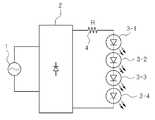
도 1은 종래의 교류 전원(1)을 사용하는 LED발광장치의 블록도이다.1 is a block diagram of an LED light emitting device using a conventional
종래의 교류 전원을 사용하는 LED 발광 장치는 브릿지 회로로 구현되는 정류 회로(2)에서 출력되는 단방향 맥류 전압을 저항(4)을 통해 고전압 LED(3-1 내지 3-4)로 제공하였다.The LED light emitting device using the conventional AC power source provides the high voltage LEDs 3-1 to 3-4 through the
이러한 종래의 교류 전원을 사용하는 LED 발광 장치에서, LED에 제공되는 LED 구동 전류는 완전한 정현파의 형태를 갖지 못하고 교류 전압과의 위상차가 발생하므로, 역률 및 전고조파 왜율(THD) 등의 전기적 특성이 LED 조명에서 요구하는 규격을 만족하지 못하는 문제가 발생할 수 있다.In such a conventional LED light-emitting device using an AC power source, the LED driving current provided to the LED does not have the form of a perfect sine wave and a phase difference occurs with the AC voltage, so that electrical characteristics such as power factor and total harmonic distortion (THD) There may be a problem that does not meet the specifications required for LED lighting.
이를 해결하기 위하여 LED의 구동 전압(순방향 전압: Vf)을 감소시키는 방법이 있으나, 고전압 구동 LED의 경우 LED의 구동 전압(Vf)에 따라서 구동효율과 광 출력 특성이 결정되기 때문에 단순히 LED의 구동 전압(Vf)을 감소시키는 것은 조명 규격에서 제시하는 역률 및 전고조파 왜율을 만족하지 못하는 문제가 발생할 수 있다.In order to solve this problem, there is a method of reducing the driving voltage (forward voltage: Vf) of the LED, but in the case of a high voltage driving LED, the driving efficiency and light output characteristics of the LED are simply determined according to the driving voltage (Vf) of the LED. Reducing (Vf) may cause problems that do not satisfy the power factor and total harmonic distortion presented in the lighting specification.
또한, 상용 교류 전원은 이상적인 정현파 형태의 교류 전압을 제공하지 못한다. 즉, 상용 교류 전압은 이상적인 정현파 형태의 기준 전압보다 그 크기가 크거나 작은 문제가 발생하고, 고조파에 의해 그 파형이 왜곡되기도 한다.In addition, commercial AC power supplies do not provide an ideal sinusoidal AC voltage. That is, the commercial AC voltage has a problem that is larger or smaller than the ideal sinusoidal reference voltage, and the waveform is distorted by harmonics.
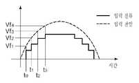
도 2A 및 도 2B는 종래의 LED 발광 장치에서 교류 전원의 변동 또는 왜곡에 따른 LED로 제공되는 전류의 파형을 시간에 따라 도시한 파형도이다.2A and 2B are waveform diagrams illustrating a waveform of current provided to an LED according to variation or distortion of an AC power source in a conventional LED light emitting device according to time.
교류 LED 구동 전류는 입력전압의 순시전압이 LED의 구동 전압(Vf)을 초과하면 입력 전압에 비례하여 전류가 흐른다. 도 2A 및 도 2B에 도시된 바와 같이, 이러한 교류 전압의 파형 변형에 의해 LED의 구동 전류가 왜곡될 수 있다. 결과적으로 LED를 교류 전원에 의해 구동하는 경우, 구동 전류의 모양과 크기에 따라 LED의 발광 효율에 매우 큰 편차가 발생하게 된다.AC LED driving current flows in proportion to the input voltage when the instantaneous voltage of the input voltage exceeds the driving voltage (Vf) of the LED. As shown in Figs. 2A and 2B, the driving current of the LED may be distorted by the waveform deformation of the AC voltage. As a result, when the LED is driven by an AC power source, a very large deviation occurs in the luminous efficiency of the LED depending on the shape and size of the driving current.
또한, 교류 전원을 이용하여 LED를 구동하기 위해서는, 정류 회로, 전원 공급 회로, 전압 검출 회로, 펄스 생성 회로, 스위치 회로, 및 전류 제어 회로와 같은 다양한 회로가 필요하다.In addition, in order to drive an LED using an AC power supply, various circuits such as a rectifier circuit, a power supply circuit, a voltage detection circuit, a pulse generation circuit, a switch circuit, and a current control circuit are required.
본 발명의 일 실시예는 LED발광장치 및 LED발광장치를 구동하는 방법을 제공한다.One embodiment of the present invention provides an LED light emitting device and a method of driving the LED light emitting device.
본 발명의 추가적 실시 형태는 다음 명세서에 의해 명시되며, 부분적으로 명세서로 명확히 될 것이다, 또는 본 발명의 실시에 의해 습득 될 수있다.Additional embodiments of the invention are set forth in the following description, and in part will be obvious from the specification, or may be learned by practice of the invention.
본 발명의 일 실시예에 따른 LED(Light-Emitting Diode)발광장치는, 교류 전원의 전압을 수신하고 교류 전원의 전압을 정류하여 단방향 맥류 전압을 출력하는 정류 회로부; 직렬로 연결된 복수의 LED부; 복수의 LED부 중 어느하나의 캐소드가 각 스위치부의 일단에 연결된 복수의 스위치부; 각각의 스위치부로부터 전류를 수신하기 위해 일단이 각 스위치의 타단과 연결된 정전류 제어회로부; 및 복수의 스위치부로부터 전류를 수신하고, 복수의 정전류 제어회로부를 순차적으로 구동하기 위해 각 스위치부를 위한 복수의 스위칭 제어신호를 생성하는 전류 비교부를 포함한다. 이때, 복수의 LED부는, 각각 단방향 맥류 전압을 수신하도록 구현되고, 애노드 및 캐소드를 포함하고, 복수의 정전류 제어회로부는, 각각의 스위치부로부터 수신한 전류의 크기가 특정 값을 갖도록 제어하기 위해 각각의 스위치부로 전류 제어 신호를 출력한다.Light-emitting diode (LED) light emitting device according to an embodiment of the present invention, the rectifier circuit unit for receiving a voltage of the AC power supply and rectifying the voltage of the AC power supply to output a unidirectional pulsed voltage; A plurality of LED units connected in series; A plurality of switch units in which one cathode of the plurality of LED units is connected to one end of each switch unit; A constant current control circuit unit having one end connected to the other end of each switch to receive current from each switch unit; And a current comparator which receives current from the plurality of switch units and generates a plurality of switching control signals for each switch unit to sequentially drive the plurality of constant current control circuit units. In this case, the plurality of LED units are implemented to receive a unidirectional pulsed voltage, respectively, and include an anode and a cathode, and the plurality of constant current control circuit units, respectively, to control the magnitude of the current received from each switch unit to have a specific value. The current control signal is output to the switch section of.
본 발명의 다른 실시예에 따른 LED발광장치를 구동하는 방법은, 정류된 교류 전압을 복수의 LED들에 가하는 단계; 제 1 LED에서 검출된 전류를 직류 전류로 변환하는 단계; 직류 전류 및 기준 전류를 비교하고, 비교한 결과에 기반하여 오차 전압 신호를 생성하는 단계; 및 오차 전압 신호 및 입력 전압 신호를 비교하고, 비교한 결과에 기반하여 PWM신호를 생성하는 단계를 포함한다. 이때, 복수의 LED들에 가하는 단계에서, 각 LED는 LED부, 및 LED부와 연결된 스위치부, 및 스위치부와 연결된 정전류 제어회로부를 포함한다.According to another aspect of the present invention, there is provided a method of driving an LED light emitting device, the method comprising: applying a rectified AC voltage to a plurality of LEDs; Converting the current detected by the first LED into a direct current; Comparing the direct current and the reference current, and generating an error voltage signal based on the comparison result; And comparing the error voltage signal and the input voltage signal, and generating a PWM signal based on the comparison result. At this time, in the step of applying to the plurality of LEDs, each LED includes an LED unit, a switch unit connected to the LED unit, and a constant current control circuit unit connected to the switch unit.
본 발명의 또 다른 실시예에 따른 LED발광장치는, 단방향 맥류 전압을 출력하기 위해 교류 전원의 전압을 수신하고 교류 전원의 전압을 정류하는 정류 회로부; 단방향 맥류 전압을 수신하기 위해 병렬로 연결된 복수의 LED채널부; 및 복수의 PWM결정 신호를 생성하기 위한 PWM신호 발생부를 포함한다. 이때, 복수의 LED채널부는 복수의 PWM결정 신호를 PWM신호 발생부로부터 각각 수신하고, 복수의 PWM결정 신호들에 반응하여 순차적으로 구동되도록 구현된다.In accordance with still another aspect of the present invention, there is provided an LED light emitting device including: a rectifying circuit unit configured to receive a voltage of an AC power source and rectify a voltage of an AC power source to output a unidirectional pulse voltage; A plurality of LED channel portions connected in parallel to receive a unidirectional pulsed voltage; And a PWM signal generator for generating a plurality of PWM decision signals. In this case, the plurality of LED channel units receive a plurality of PWM determination signals from the PWM signal generator, respectively, and are implemented to be sequentially driven in response to the plurality of PWM determination signals.
본 발명의 또 다른 실시예에 따른 LED발광장치를 구동하는 방법은, 교류 전원의 전압을 수신하는 단계; 교류 전원 전압을 정류하여 단방향 맥류 전압을 출력하는 단계; 병렬로 연결된 복수의 LED채널부로 단방향 맥류 전압을 인가하는 단계; 복수의 PWM결정 신호를 생성하는 단계; 및 복수의 LED채널부를 순차적으로 구동하기 위해 복수의 LED채널부로 복수의 PWM결정 신호를 각각 인가하는 단계를 포함한다.According to still another aspect of the present invention, there is provided a method of driving an LED light emitting device, the method comprising: receiving a voltage of an AC power source; Rectifying the AC power supply voltage to output a unidirectional pulsed voltage; Applying a unidirectional pulse voltage to a plurality of LED channel portions connected in parallel; Generating a plurality of PWM decision signals; And applying a plurality of PWM decision signals to the plurality of LED channel units, respectively, to sequentially drive the plurality of LED channel units.
본 발명의 또 다른 실시예에 따른 LED발광장치는, 교류 전압을 수신하고, 정류된 전압을 생성하기 위해 교류 전압을 정류하는 정류기; 정류된 전압을 수신하기 위해 병렬로 연결된 제 1 및 제 2 LED채널부; 및 제 1 PWM결정 신호 및 제 2 PWM결정 신호를 생성하는 PWM신호 발생부를 포함한다. 이때, 제 1 및 제 2 LED채널부는 각각 제 1 PWM결정 신호 및 제 2 PWM결정 신호를 수신하고, 제 1 및 제 2 LED채널부는 제 1 및 제 2 PWM결정 신호들에 반응하여 순차적으로 구동된다.In accordance with still another aspect of the present invention, there is provided an LED light emitting device including: a rectifier configured to receive an AC voltage and rectify the AC voltage to generate a rectified voltage; First and second LED channel portions connected in parallel to receive a rectified voltage; And a PWM signal generator for generating a first PWM decision signal and a second PWM decision signal. In this case, the first and second LED channel units receive the first PWM determination signal and the second PWM determination signal, respectively, and the first and second LED channel units are sequentially driven in response to the first and second PWM determination signals. .
앞서 언급한 일반적인 설명 및 후술할 상세한 설명은 예시적인 것에 불과하고, 청구한 발명의 추가적 설명을 제공하기 위한 것이다.The foregoing general description and the following detailed description are exemplary only, and are intended to provide further explanation of the claimed invention.
첨부된 도면은 본 발명의 추가적인 이해를 제공하기 위해 포함되었으며, 본 명세서의 일부분을 구성하는 것으로, 본 발명의 실시예를 도시하며, 명세서와 함께 본 발명의 원리를 설명하는 역할을 한다.
도 1은 종래의 교류 전원을 사용하는 LED발광장치의 블록도이다.
도 2A 및 도 2B는 도 1에서 도시한 종래의 LED발광장치의 전류의 파형을 보여준다.
도 3은 본 발명의 일 실시예에 따른 교류 전원을 사용하는 LED발광장치의 블록도이다.
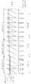
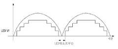
도 4는 도 3의 LED발광장치에 있는 LED들에게 공급하기 위한 교류 전압과 교류 전류의 파형이다.
도 5는 교류 전원을 이용한 도 3의 LED발광장치에 제공되는 스위치의 제어 신호의 파형이다.
도 6은 본 발명의 일 실시예에 따른 교류 전원을 사용하는 LED발광장치이다.
도 7은 본 발명의 일 실시예에 따른 다단 전류 구동을 이용하여 LED들에게 공급되는 교류 전압 및 전류의 파형이다.
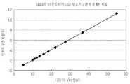
도 8은 동일한 구동 전압을 갖는 복수의 LED부가 본 발명의 일 실시예에 따른 교류 전원을 사용하는 LED발광장치에서 직렬로 연결된 경우, LED오프 구간 비율 대비 LED들의 개수를 보여주는 그래프이다.
도 9는 도 3에 도시된 본 발명의 일 실시예에 따른 교류 전원을 사용하는 LED발광장치에서 제 1 다이오드의 구동 전압과 오프 구간의 관계를 보여주는 그래프이다.
도 10은 본 발명의 일 실시예에 따른 교류 전원을 사용하는 LED발광장치에서, LED들에게 공급되는 교류 전압과 교류 전류의 파형이다.
도 11은 다단 전류를 구동하는 동안 LED들에게 제공되는 교류 전압과 전류 파형이다.
도 12는 본 발명의 일 실시예에 따른 LED발광장치이다.
도 13은 도 12에 기반한 교류 전원을 사용하는 LED발광장치를 상세하게 도시한다.
도 14는 도 13에 도시한 본 발명의 일 실시예에 따른 교류 전원을 사용하는 LED발광장치의 평균 전류 제어회로부의 펄스 폭 변조(Pulse Width Moldulation, PWM)출력신호의 파형이다.
도 15는 다단 PWM전류 구동에 따라 LED들에게 공급되는 교류 전압과 전류의 파형이다.
도 16은 본 발명의 일 실시예에 따른 LED발광장치이다.
도 17은 도 16에 도시된 본 발명의 일 실시예에 따른 LED발광장치의 LED채널을 보다 상세하게 도시한다.
도 18은 본 발명의 일 실시예에 따른 LED발광장치의 주파수 분주 얻은 PWM결정 신호의 파형이다.
도 19는 본 발명의 일 실시예에 따른 LED발광장치의 PWM 를 보여주는 보다 상세한 블록도이다.
도 20은 도 19에서 도시한 본 발명의 일 실시예에 따른 LED발광장치의 PWM출력신호에 따라 변하는 LED구동 전류의 파형이다.
도 21은 본 발명의 일 실시예에 따른 LED발광장치이다.
도 22A 및 도 22B는 도 21에서 도시한 본 발명의 일 실시예에 따른 LED발광장치의 개선된 LED오프 구간이 있을 때와 없을 때 각각의 LED구동 전류 파형이다.
도 23은 본 발명의 일 실시예에 따른 LED발광장치의 주파수 분주에서 얻은 PWM결정 신호 파형이다.
도 24는 도 23에서 도시한 본 발명의 일 실시예에 따른 LED발광장치의 PWM출력 신호에 따라 변하는 LED구동 전류의 파형이다.
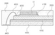
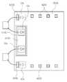
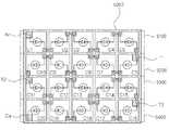
도 25는 본 발명의 일 실시에에 따른 LED구동 회로 패키지로서 실행되는 LED구동 회로이다.
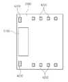
도 26은 본 발명의 일 실시예에 따른 LED구동 회로 패키지의 평면도이다.
도 27은 도 26에서 도시한 본 발명의 일 실시예에 따른 LED구동 회로 패키지의 측면도이다.
도 28은 본 발명의 일 실시에에 따른 LED구동 회로 패키지로서 실행되는 LED구동 회로이다.
도 29는 도 28에서 도시한 본 발명의 일 실시예에 따른 LED구동 회로 패키지의 측면도이다.
도 30 및 도 31은 본 발명의 일 실시예에 따른 및 도 28의 LED구동 회로 패키지에 있는 실리콘 기판의 표면 위에 있는 단자들의 배치, 정류부의 구현의 예를 보여주는 평면도이다.
도 32는 본 발명의 일 실시예에 따른 LED구동 회로 패키지에 있는 전극 패드의 배치, 및 전극 패드와 LED이다.
도 33은 본 발명의 일 실시예에 따른 LED구동 회로 패키지에 있는 전극 패드의 배치, 및 전극 패드와 방열 패드 사이의 연결이다.
도 34는 본 발명의 일 실시예에 따른 LED구동 회로 패키지가 적용되는 발광 모듈의 일 예이다.
도 35는 도 3, 도4, 도 5, 및 도6에 관하여 상술한 본 발명의 LED발광장치에 적용될 수 있는 LED칩의 일 예이다.
도 36은 도 35에서 도시한 멀티 셀 LED칩을 이용한 LED패키지를 보여주는 평면도이다.
도 37A 및 도 37B은 도 35및 도 36에서 도시한 실시예들에 따른 LED발광장치에 적용될 수 있는 LED패키지의 실시예이다.
도 38A 및 도 38B는 도 35및 도 36에서 도시한 LED발광장치에 적용될 수 있는 LED패키지의 실시예이다.
도 39는 도 3과 관련하여 상술한 실시예에 따른 교류 전원을 사용하는 LED발광장치에서, LED들에게 제공되는 교류 전류의 오프 구간의 파형이다.
도 40은 본 발명의 일 실시예에 따른 교류 전원을 사용하는 LED발광장치에서, LED들에게 공급되는 교류 전압과 교류 전류의 파형이다.
도 41은 도 40에서 도시한 실시예에 따른 교류 전원을 사용하는 LED발광장치에서, LED들에게 공급되는 교류 전압과 교류 전류의 파형이다.
도 42는 시간이 지남에 따른, 도 40의 실시예에 따른 교류 전원을 사용하는 LED발광장치에서 공급된 스위치의 제어 신호 파형, 스위치를 통해 흐르는 전류의 파형, 및 LED들에게 공급된 전류의 파형이다.The accompanying drawings are included to provide a further understanding of the invention, and are a part of this specification, illustrate embodiments of the invention and, together with the description, serve to explain the principles of the invention.
1 is a block diagram of a LED light emitting device using a conventional AC power supply.
2A and 2B show waveforms of current of the conventional LED light emitting device shown in FIG.
3 is a block diagram of an LED light emitting device using an AC power supply according to an embodiment of the present invention.
4 is a waveform of AC voltage and AC current for supplying LEDs in the LED light emitting device of FIG. 3.
5 is a waveform of a control signal of a switch provided to the LED light emitting device of FIG. 3 using an AC power source.
6 is an LED light emitting device using an AC power supply according to an embodiment of the present invention.
7 is a waveform of AC voltage and current supplied to LEDs using multi-stage current driving according to an embodiment of the present invention.
8 is a graph showing the number of LEDs compared to the ratio of LED off intervals when a plurality of LED units having the same driving voltage are connected in series in an LED light emitting device using AC power according to an embodiment of the present invention.
FIG. 9 is a graph showing a relationship between a driving voltage and an off period of a first diode in the LED light emitting device using the AC power source according to an embodiment of the present invention shown in FIG. 3.
10 is a waveform of an AC voltage and an AC current supplied to the LEDs in the LED light emitting device using the AC power according to an embodiment of the present invention.
11 is an alternating voltage and current waveform provided to the LEDs while driving the multi-stage current.
12 is an LED light emitting device according to an embodiment of the present invention.
FIG. 13 illustrates in detail an LED light emitting device using an AC power source based on FIG. 12.
14 is a waveform of a pulse width modulation (PWM) output signal of an average current control circuit of an LED light emitting device using an AC power source according to an embodiment of the present invention shown in FIG. 13.
15 is a waveform of AC voltage and current supplied to LEDs according to multi-stage PWM current driving.
16 is an LED light emitting device according to an embodiment of the present invention.
FIG. 17 illustrates the LED channel of the LED light emitting device according to the embodiment of the present invention shown in FIG. 16 in more detail.
18 is a waveform of a PWM determination signal obtained by frequency division of an LED light emitting device according to an embodiment of the present invention.
19 is a more detailed block diagram showing a PWM of an LED light emitting device according to an embodiment of the present invention.
20 is a waveform of an LED driving current that changes according to the PWM output signal of the LED light emitting device according to an embodiment of the present invention shown in FIG.
21 is an LED light emitting device according to an embodiment of the present invention.
22A and 22B are respective LED driving current waveforms with and without an improved LED off period of the LED light emitting device according to the embodiment of the present invention shown in FIG.
23 is a PWM decision signal waveform obtained from the frequency division of the LED light emitting device according to an embodiment of the present invention.
FIG. 24 is a waveform of LED driving current changing according to the PWM output signal of the LED light emitting device according to the embodiment of FIG. 23.
25 is an LED drive circuit executed as an LED drive circuit package according to an embodiment of the present invention.
26 is a plan view of an LED driving circuit package according to an embodiment of the present invention.
FIG. 27 is a side view of the LED driving circuit package according to the embodiment of the present invention shown in FIG. 26.
28 is an LED drive circuit executed as an LED drive circuit package according to an embodiment of the present invention.
29 is a side view of the LED driving circuit package according to the embodiment of the present invention shown in FIG. 28.
30 and 31 are plan views illustrating examples of arrangement of terminals and rectifiers on the surface of the silicon substrate in the LED drive circuit package of FIG. 28 according to one embodiment of the present invention.
32 is an arrangement of electrode pads in an LED drive circuit package, and electrode pads and LEDs in accordance with one embodiment of the present invention.
33 is a layout of the electrode pads in the LED drive circuit package and the connection between the electrode pads and the heat dissipation pads according to an embodiment of the present invention.
34 is an example of a light emitting module to which an LED driving circuit package according to an embodiment of the present invention is applied.
35 is an example of an LED chip that can be applied to the LED light emitting device of the present invention described above with reference to FIGS. 3, 4, 5, and 6.
FIG. 36 is a plan view illustrating an LED package using the multi-cell LED chip illustrated in FIG. 35.
37A and 37B illustrate embodiments of an LED package applicable to the LED light emitting device according to the embodiments shown in FIGS. 35 and 36.
38A and 38B illustrate an embodiment of an LED package applicable to the LED light emitting device shown in FIGS. 35 and 36.
FIG. 39 is a waveform of an off period of AC current provided to LEDs in the LED light emitting device using the AC power source according to the embodiment described above with reference to FIG. 3.
40 is a waveform of AC voltage and AC current supplied to LEDs in the LED light emitting device using the AC power according to the embodiment of the present invention.
FIG. 41 is a waveform of AC voltage and AC current supplied to LEDs in the LED light emitting device using the AC power source according to the embodiment shown in FIG. 40.
FIG. 42 is a waveform of a control signal of a switch supplied from an LED light emitting device using an AC power source according to the embodiment of FIG. 40, a waveform of current flowing through the switch, and a waveform of current supplied to the LEDs over time. to be.
본 발명은 이하 본 발명의 실시예가 표시되는 첨부된 도면을 참조하여 완전히 설명된다. 그러나 본 발명은 다양한 형태로 구현될 수 있으며 여기에 명시된 실시예에 한정되는 것으로 해석되어서는 안된다. 오히려 이러한 실시예는 해당 개시가 철저하도록 하고, 당업자에게 완벽하게 본 발명의 범위를 전달하기 위해 제공된다. 도면에서, 크기 및 계층 및 지역의 상대적 크기는 명확성을 위해 과장될 수 있다. 도면에 제시된 동일한 참조 부호는 동일한 부재를 지칭한다.The invention is now fully described with reference to the accompanying drawings, in which embodiments of the invention are shown. However, the present invention may be embodied in various forms and should not be construed as limited to the embodiments set forth herein. Rather, these embodiments are provided so that this disclosure will be thorough, and will fully convey the scope of the invention to those skilled in the art. In the drawings, the size and relative sizes of layers and regions may be exaggerated for clarity. Like reference numerals in the drawings refer to like elements.
구성 요소나 계층이 "~상에" 또는 다른 구성 요소 또는 계층과 "연결"되었다고 언급되고 있는 경우, 접적으로 다른 구성 요소 또는 계층 위에 놓이거나 직접적으로 연결된 것을 의미할 수 있고, 그 사이에 다른 구성 요소나 계층이 존재함을 의미할 수 있다. 반대로, "직접적으로 ~상에" 또는 "직접적으로 연결"되었다고 언급되고 있는 경우, 그 사이에 다른 구성 요소나 계층이 존재하지 않음을 의미한다.When a component or layer is said to be "on" or "connected" to another component or layer, it may mean that it is directly on or directly connected to another component or layer, with other components in between. This may mean that an element or hierarchy exists. Conversely, when referred to as "directly on" or "directly connected", it means that there are no other components or layers in between.
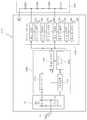
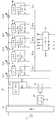
도 3은 본 발명의 일 실시예에 따른 교류 전원을 사용하는 LED발광장치의 블록도이다.3 is a block diagram of an LED light emitting device using an AC power supply according to an embodiment of the present invention.
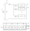
도 3을 참조하면, 본 발명의 실시예에 따른 교류 전원을 사용하는 LED발광장치는 교류 전원(11), 정류회로부(12), 복수의 LED부(13-1 내지 13-N), 복수의 스위치(14-1 내지 14-(N-1)), 정전류 제어회로부(15-1 내지 15-(N-1)), 및 전류 비교부(16)를 포함할 수 있다.Referring to FIG. 3, an LED light emitting device using an AC power source according to an embodiment of the present invention includes an
교류 전원(11)은 상용 교류 전원이 될 수 있고, 정현파 형태의 교류 전압을 공급할 수 있다.The
정류회로부(12)는 교류 전원(11)으로부터 공급된 교류 전압을 정류하여 단방향 맥류 전압을 생성할 수 있다. 또한, 정류회로부(12)는 복수의 다이오드를 이용하여 구현된 브릿지 회로일 수 있다.The
복수의 LED부(13-1내지 13-N)는 상호 직렬 연결될 수 있다. 이때, 정류회로부(12)의 한 단자는 LED부(13-1)의 애노드에 연결되고, LED부(13-1)의 캐소드는 다른 LED부(13-2)의 애노드에 연결된다. LED부(13-2)의 캐소드는 다른 LED부(13-3)의 애노드와 연결되고, 마찬가지로 LED부(13-3)의 캐소드는 다른 LED부(13-4)의 애노드에 연결되는 등 계속적으로 연결된다. 도 3에서 도시한 13-1내지 13-N까지의 각 LED부는 하나의 LED일 수 있고, 동일 극성이 상호 연결된(즉, 병렬 연결된) 복수의 LED를 포함할 수 있다. 여기서 직렬 연결되는 LED의 수는 구동회로 의 효율 향상과 다단계 전류제어를 목적으로 확장시킬 수 있다.The plurality of LEDs 13-1 to 13 -N may be connected in series with each other. At this time, one terminal of the
각 스위치(14-1내지 14-(N-1))는, 복수의 LED부(13-1내지 13-N)에 포함된 각각의 LED부가 상호 연결된 노드에 일단이 연결될 수 있다. 즉, 제 1 LED부(13-1)와 제 2 LED부(13-2)의 연결 노드에 제 1 스위치(14-1)가 연결될 수 있고, 제 2 LED부(13-2)와 제 3 LED부(13-3) 사이에 제 2 스위치(14-2)가 연결될 수 있다. 즉, 제 (N-1) LED부(13-(N-1))와 제 N LED부(13-N) 사이에 제 (N-1) 스위치(14-(N-1))가 연결될 수 있다.Each switch 14-1 to 14- (N-1) may be connected to one end of each of the LED units included in the plurality of LED units 13-1 to 13-N. That is, the first switch 14-1 may be connected to the connection node of the first LED unit 13-1 and the second LED unit 13-2, and the second LED unit 13-2 and the third LED may be connected to each other. The second switch 14-2 may be connected between the LED units 13-3. That is, the (N-1) th switch 14- (N-1) may be connected between the (N-1) th LED portion 13- (N-1) and the Nth LED portion 13-N. have.
이러한 스위치(14-1내지 14-(N-1))는 후술하는 바와 같이 전류 비교부(16)에서 출력된 스위칭 제어 신호(S1내지 SN)에 따라 동작할 수 있다. 또한, 스위치(14-1내지 14-N)는 정전류 제어회로부(15-1내지 15-N)의 제어 신호에 따라 동작할 수 있다.The switches 14-1 to 14- (N-1) may operate according to the switching control signals S1 to SN output from the
정전류 제어회로부(15-1내지 15-N)는 복수의 LED부(13-1내지 13-N)를 통해 흐르는 전류를 일정한 크기로 제어할 수 있다. 정전류 제어회로부(15-1내지 15-(N-1))는 스위치(14-1내지 14-N)의 타단에 연결될 수 있다.The constant current control circuit unit 15-1 to 15 -N may control the current flowing through the plurality of LED units 13-1 to 13 -N to a predetermined size. The constant current control circuit unit 15-1 to 15-(N-1) may be connected to the other end of the switch 14-1 to 14 -N.
전류비교부(16)는 정전류 제어 회로 유닛(15-1 내지 15-N)에 의해 각각 제어되는 스위치(14-2 내지 14-N)의 개방에 따라 스위치(14-1 내지 14-N)에 흐르는 전류(i2 내지iN)을 수신한다. 보다 상세하게는, 전류 비교부(16)는 정전류 제어회로부(15-1내지 15-N)가 순차적으로 동작하게 하도록, 스위치(14-1내지 14-N)를 단락하거나 (턴온) 또는 개방하는(턴오프) 스위칭 제어 신호(S1내지 SN)를 생성한다. 즉, 후단의 전류(i2내지 iN)를 입력받아 그중 어느 하나의 전류가 기설정된 값이 되면, 각 스위칭 제어 신호(S1내지 SN)는 대응하는 스위치(14-1내지 14-N)를 개방 상태(턴오프)로 전환시킨다. 예를 들어, 후단의 전류(i2내지 iN)가 수신되고, 그 중 어느 전류가 기설정된 값에 도달한 경우, 제 1 스위칭 제어 신호(S1)가 제 1 스위치(14-1)를 개방 상태(턴오프)로 전환시킨다. 그리고, 후단의 전류(i3내지 iN)가 수신되고, 그 중 어느 전류가 기설정된 값에 도달한 경우, 제 2 스위칭 제어 신호(S2)가 제 2 스위치(14-2)를 개방 상태(즉, 턴오프 상태)로 전환시킨다. 또한, 후단의 전류(iN)가 수신되고, 대응하는 전류가 기설정된 값에 도달한 경우, 제 (N-1) 스위칭 제어 신호(S(N-1))가 제 (N-1) 스위치(14-(N-1))를 개방상태로 전환시킨다.The current comparing
도 3에 도시된 본 발명의 일 실시예에 따른 교류 전원을 사용하는 LED발광장치의 동작에 대하여 이하 상세히 설명한다.The operation of the LED light emitting device using the AC power source according to the embodiment of the present invention shown in FIG. 3 will be described in detail below.
먼저, 교류 전원(11)에 의해 교류 전압이 정류회로부(12)로 입력되면, 정류회로부(12)는 교류 전압을 정류한 후, 단방향 맥류 전압을 출력한다. 도 3에 도시된 바와 같이, 정류회로부(12)로 입력되는 교류 전원(11)의 출력 전압은 정의 방향과 부의 방향을 모두 갖는 교류 전압이며, 정류회로부(12)에서 출력되는 전압은 부의 방향의 전압을 정의 방향으로 변환한 단 방향의 맥류 전압의 형태를 갖는다. 이러한 맥류 전압이 복수의 LED부(13-1 내지 13-N)에 제공된다.First, when an AC voltage is input to the
이어서, 맥류 전압이 증가하면, LED부(13-1내지 13-N)는 순차적으로 발광할 수 있다. 이러한 LED부의 발광 동작은 이하 도 4 및 도 5와 관련하여 후술한다.Subsequently, when the pulse voltage is increased, the LEDs 13-1 to 13 -N may emit light sequentially. The light emitting operation of the LED unit will be described later with reference to FIGS. 4 and 5.
도 4는 본 발명의 일 실시예에 따른 교류 전원을 사용하는 LED발광장치에 있는 LED들에게 공급되는 교류 전압 및 교류전류의 파형이다.4 is a waveform of an AC voltage and an AC current supplied to LEDs in an LED light emitting device using an AC power source according to an embodiment of the present invention.
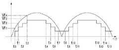
또한, 도 5는 본 발명의 일 실시예에 따른 교류 전원을 사용하는 LED장치에서 제공되는 스위치의 제어 신호 파형, 스위치를 통해 흐르는 전류의 파형, 및 지속적으로 LED로 제공되는 교류 전류의 파형이다.5 is a waveform of a control signal of a switch provided in an LED device using an AC power source, a waveform of a current flowing through the switch, and a waveform of an AC current continuously provided to the LED.
도 4 및 도 5는 LED부의 숫자가 네 개, 즉, N=4인 경우이다. 따라서, 이하에서는 N이 4로 설정된 도 3의 경우에 대하여 기술한다. 또한, 도 4 및 도 5는 정류회로부(12)에 의해 공급되는 맥류 전압의 한 주기에 대해서만 도시한다. 동일한 동작이 맥류 전압의 남아있는 주기에서 수행되기 때문에, 나머지 주기에 대한 기술은 생략한다.4 and 5 show four LED parts, that is, N = 4. Therefore, hereinafter, the case of FIG. 3 in which N is set to 4 will be described. 4 and 5 only show one cycle of the pulse current voltage supplied by the
LED부(13-1내지 13-4) 측으로 제공되는 맥류 전압의 크기가 증가하여 제 1 LED부(13-1)의 구동 전압(순방향 전압 Vf1)에 도달하면(도 4 및 도 5의 t0), 전류는 제 1 LED부(13-1)를 통해 흐르고, 발광이 된다.When the magnitude of the pulse flow voltage provided to the LED parts 13-1 to 13-4 increases and reaches the driving voltage (forward voltage Vf1) of the first LED part 13-1 (t0 in FIGS. 4 and 5). ), Current flows through the first LED unit 13-1 to emit light.
여기서, 제 1 스위치(14-1) 내지 제 4 스위치(14-4)는 초기에 단락 상태(턴온)로 설정된다. 이러한 입력 전압(Vf1)은 제 1 LED부(13-1)를 턴온시키는 전압으로서, 이에 대응하는 전류는 제 1 LED부(13-1)를 통하여 제 1 정전류 제어회로부(15-1)로의 경로를 따라 흐른다. 이때, 제 1 스위치(14-1)는 제 1 정전류 제어회로부(15-1-)의 출력인 제어 신호에 따라 제 1 정전류 제어회로부(15-1)를 통과하는 전류를 일정하게 제어한다. 제 1 정전류 제어회로부(15-1)는, 제 1 LED부(13-1)를 구동하도록 기설정된 기준 전류가 제 1 LED부(13-1)를 통해 흐를 수 있게 하기 위하여, 정전류 제어를 수행한다. 제 1 LED부(13-1)가 발광하기 시작하는 동작은 시간 구간t0- t1에 대응한다.Here, the first switch 14-1 to the fourth switch 14-4 are initially set to a short circuit state (turn on). The input voltage Vf1 is a voltage for turning on the first LED unit 13-1, and a current corresponding thereto passes through the first LED unit 13-1 to the first constant current control circuit unit 15-1. Flows along. At this time, the first switch 14-1 constantly controls the current passing through the first constant current control circuit unit 15-1 according to a control signal output from the first constant current control circuit unit 15-1-. The first constant current control circuit unit 15-1 performs constant current control in order to allow a reference current preset to drive the first LED unit 13-1 to flow through the first LED unit 13-1. do. The operation in which the first LED unit 13-1 starts to emit light corresponds to the time interval t0 -t1 .
이어, 맥류 전압의 크기가 더욱 증가하여, 제 2 LED부(13-2)에 인가되는 전압이 제 2 LED부(13-2)의 구동 전압이 되면(맥류 전압의 크기가 Vf2가 되면), 제 2 LED부(13-2)에 전류가 흘러 발광된다(도 4 및 도 5의 t1시점). 여기서, 이러한 입력전압(Vf2)은 제 1 LED부(13-1) 및 제 2 LED부(13-2)를 턴온시킬 수 있는 전압으로서, 이에 대응하는 전류는 제 2 LED(13-2)를 통하여 제 2 정전류 회로제어부(15-2)로의 경로를 따라서 흐른다. 이때, 전류비교부(16)는 제 2 정전류 제어회로부(15-2)의 전류(i2)가 기설정된 값임을 검출하여 제 1 스위칭 제어신호(S1)를 생성하여 제 1 스위치(14-1)를 개방(턴오프)시킨다. 이와 동시에, 제 2 스위치(14-2)는 제 2 정전류 제어회로부(15-2)의 제어신호에 따라 턴온을 유지하며, 제 2 정전류 제어회로부(15-2) 를 통과하여 흐르는 전류를 제 1 및 제 2 LED부(13-1 및 13-1)를 구동하기 위해 사전 설정된 기준 전류가 되도록 제어한다.Subsequently, the magnitude of the pulse voltage increases further, and when the voltage applied to the second LED portion 13-2 becomes the driving voltage of the second LED portion 13-2 (when the magnitude of the pulse voltage is Vf 2), Current flows through the second LED unit 13-2 (t1 in FIGS. 4 and 5). Viewpoint). Here, the input voltage Vf2 is a voltage capable of turning on the first LED unit 13-1 and the second LED unit 13-2, and a current corresponding thereto causes the second LED 13-2 to turn on. It flows along the path to the 2nd constant current circuit control part 15-2 through. At this time, the
이러한 동작을 통해, 제 1 LED부(13-1)와 제 2 LED부(13-2)에 일정한 전류가 흐르도록 제어될 수 있다. 또한, 도 4 및 도 5에 도시한 바와 같이, t1 시점에서 제 1 스위치(14-1)가 턴오프 되고, 제 2 정전류 제어회로부(15-1)의 정전류 제어에 의해 계단 형태의 입력 전류를 형성할 수 있다.Through this operation, a constant current may be controlled to flow in the first LED unit 13-1 and the second LED unit 13-2. 4 and 5, the first switch 14-1 is turned off at time t1 and the stepped input current is controlled by the constant current control of the second constant current control circuit unit 15-1. Can be formed.
전술한 것과 유사하게, 맥류 전압이 더욱 증가하여 제 3 LED부(13-3)에 인가되는 전압이 제 3 LED부(13-3)의 구동 전압이 되면(맥류 전압의 크기가 Vf3가 되면), 제 3 LED부(13-3)에 전류가 흘러 발광된다(도 4 및 도 5의 t2 시점). 여기서, 이러한 입력전압(Vf3)은 제 1 LED부(13-1) 내지 제 3 LED부(13-3)를 턴온시킬 수 있는 전압으로서, 이에 대응하는 전류는 제 3LED(13-3)를 통하여 제 3 정전류 회로제어부(15-3)로의 경로를 따라서도 흐른다. 이때, 전류비교부(16)는 제 3 정전류 제어회로부(15-3)의 전류(i3)가 기설정된 값임을 검출하여 제 1 및 제 2 스위칭 제어신호 (S1 및 S2)를 생성하여 제 1 및 제 2 스위치(14-1 및 14-2)를 개방(턴오프)시킨다. 이와 동시에, 제 3 스위치(14-3)는 제 3 정전류 제어회로부(15-3)의 제어신호에 따라 턴온을 유지하며, 제 3 정전류 제어회로부(15-3) 를 통과하여 흐르는 전류를 제 1 내지 제 3 LED부(13-1 내지 13-3)를 구동하기 위해 사전 설정된 기준 전류가 되도록 제어한다.Similar to the above, when the pulse voltage is further increased so that the voltage applied to the third LED portion 13-3 becomes the driving voltage of the third LED portion 13-3 (when the magnitude of the pulse voltage is Vf3). The current flows through the third LED unit 13-3 and emits light (t2 time points in FIGS. 4 and 5). Here, the input voltage Vf3 is a voltage capable of turning on the first LED unit 13-1 to the third LED unit 13-3, and a current corresponding thereto is transmitted through the third LED 13-3. It also flows along the path to the third constant current circuit control unit 15-3. At this time, the current comparing
이러한 동작을 통해, 제 1 LED부(13-1)와 제 2 LED부(13-2) 및 제 3 LED부(13-3)에 일정한 전류가 흐르도록 제어될 수 있다. 또한, 도 4 및 도 5에 도시한 바와 같이, t2 시점에서 제 1 스위치(14-1) 및 제 2 스위치(14-2)가 턴오프 되고, 제 3 정전류 제어회로부(15-1)의 정전류 제어에 의해 계단 형태의 입력 전류를 형성할 수 있다.Through this operation, a constant current may be controlled to flow in the first LED unit 13-1, the second LED unit 13-2, and the third LED unit 13-3. 4 and 5, the first switch 14-1 and the second switch 14-2 are turned off at a time t2 , and the third constant current control circuit unit 15-1 is turned off. The constant current control can form a stepped input current.
전술한 것과 유사하게, 맥류 전압이 더욱 증가하여 제 4 LED부(13-4)에 인가되는 전압이 제 4 LED부(13-4)의 구동 전압이 되면(맥류 전압의 크기가 Vf4가 되면), 제 4 LED부(13-4)에 전류가 흘러 발광된다(도 4 및 도 5의 t3 시점). 여기서, 이러한 입력전압(Vf4)은 제 1 LED부(13-1) 내지 제 4 LED부(13-4) 모두 턴온시킬 수 있는 전압으로서, 이에 대응하는 전류는 제 4 LED부(13-4)를 통하여 제 4 정전류 회로제어부(15-4)로의 경로를 따라서도 흐른다. 이때, 전류 비교부(16)는 제 4 정전류 제어회로부(15-4)의 전류(i4)가 기설정된 값임을 검출하여 제 1 내지 제 3 스위칭 제어신호(S1 내지 S3)를 생성하여 제 1 내지 제 3 스위치(14-1 내지 14-3)를 개방(턴오프)시킨다. 이와 동시에, 제 4 스위치(14-4)는 제 4 정전류 제어회로부(15-4)의 제어신호에 따라 턴온을 유지하며, 제 4 정전류 제어회로부(15-4) 를 통과하여 흐르는 전류를 제 1 내지 제 4 LED부(13-1 내지 13-4)를 구동하기 위해 사전 설정된 기준 전류가 되도록 제어한다.Similar to the above, when the pulse voltage is further increased so that the voltage applied to the fourth LED part 13-4 becomes the driving voltage of the fourth LED part 13-4 (when the magnitude of the pulse voltage is Vf4). The current flows through the fourth LED unit 13-4 and emits light (time t3 in FIGS. 4 and 5). Here, the input voltage Vf4 is a voltage that can turn on all of the first LED unit 13-1 to the fourth LED unit 13-4, and the current corresponding thereto is the fourth LED unit 13-4. It also flows along the path to the fourth constant current circuit control unit 15-4 through. At this time, the
이러한 동작을 통해, 제 1 LED부(13-1), 제 2 LED부(13-2), 제 3 LED부(13-3) 및 제 4 LED부(13-4)에 일정한 전류가 흐르도록 제어될 수 있다. 또한, 도 4 및 도 5에 도시한 바와 같이, t3 시점에서 제 3 스위치가 턴오프 되고, 제 4 정전류 제어회로부(15-4)의 정전류 제어에 의해 계단 형태의 입력전류를 형성할 수 있다.Through this operation, a constant current flows in the first LED unit 13-1, the second LED unit 13-2, the third LED unit 13-3, and the fourth LED unit 13-4. Can be controlled. In addition, as shown in FIGS. 4 and 5, the third switch is turned off at time t3 , and a stepped input current can be formed by the constant current control of the fourth constant current control circuit unit 15-4. .
맥류 전압이 피크를 지나, 점차 감소하는 경우, LED부는 제 4 LED부(13-4)부터 제 1 LED부(13-1)까지 순차적으로 턴오프된다. 제 4 LED부(13-4)가 꺼진 경우(t4시점), 전류 비교부(16)는 제 4 정전류 제어회로부의 전류(i4)가 기설정된 값이 아님을 검출하고, 제 4 스위칭 제어 신호(S4)를 바꿔서 제 3 스위치(14-3)를 단락시킨다(턴온). 이 경우, 제 1 및 제 2 스위칭 제어 신호(S1 및 S2)는 이전의 상태가 유지되므로, 제 1 및 제 2 스위치(14-1 및 14-2)가 개방 상태(턴오프)로 유지된다. 이와 동시에, 제 3 정전류 제어회로부(15-3)를 통해 흐르는 전류가 제 1 내지 제 3 LED부(13-1내지 13-4)를 구동하도록 기설정된 기준 전류가 되게 하기 위해, 제 3 정전류 제어회로부(15-3)의 출력인 제어 신호에 따라, 제 3 스위치(14-3)는 정전류 제어를 시작한다.When the pulse voltage is gradually decreased after the peak, the LED unit is sequentially turned off from the fourth LED unit 13-4 to the first LED unit 13-1. When the fourth LED part 13-4 is turned off (t4 Time point), the
이후의 전류 제어 동작은, 상술한 t0- t3구간 동안 수행되는 정전류 제어의 역순이므로, 상세한 설명은 생략하기로 한다.Since the current control operation is the reverse order of the constant current control performed during the aforementioned t0 -t3 interval, detailed description thereof will be omitted.
본 실시예에서는 다단 정전류 제어에 의해 계단 형태로 LED구동 전류가 증가하거나 감소하는 경우에 대해 상술하였으나, 본 발명은 이에 한정되지 아니하고, LED구동 전류의 파형은 정전류 제어를 위한 기준 전류를 다양하게 변경함으로서 변경될 수 있다.In the present embodiment, the case in which the LED driving current increases or decreases in a step shape by the multi-stage constant current control has been described above. However, the present invention is not limited thereto, and the waveform of the LED driving current is variously changed in the reference current for the constant current control. Can be changed.
도 6은 본 발명의 다른 실시예에 따른 교류 전원을 사용하는 LED발광장치이다.6 is an LED light emitting device using an AC power supply according to another embodiment of the present invention.
도 6에 도시된 바와 같은 다른 실시예에 따른 LED발광장치가 LED 발광부(13-1-1 내지 13-N-M)를 제외한 구성이 상기 실시예와 동일하므로 여기서 그 설명은 생략한다.Since the configuration of the LED light emitting device according to another embodiment as shown in FIG. 6 except for the LED light emitting units 13-1 to 13 -N-M is the same as that of the above embodiment, a description thereof will be omitted herein.
본 발명의 일 실시예에서, 각 LED부는 복수의 LED가 병렬로 각각 연결되도록 구현되었다. 예를 들어, 제 1 LED부(13-1-1내지 13-1-M)는 M개의 LED가 각각 병렬로 연결되도록 구현되었다. 여기서, 병렬로 연결된 LED의 수는, LED조명 램프의 광속을 증가시키기 위해 또는 발광 램프의 용량을 증설시키기 위해 확장될 수 있다. In one embodiment of the present invention, each LED unit is implemented such that a plurality of LEDs are respectively connected in parallel. For example, the first LED units 13-1-1 to 13-1-M are implemented such that M LEDs are connected in parallel. Here, the number of LEDs connected in parallel can be extended to increase the luminous flux of the LED lighting lamp or to increase the capacity of the light emitting lamp.
이와 같이, 본 발명은 교류 전압을 이용하여 상호 직렬 연결된 LED 를 순차적으로 정전류 구동함으로써, 도 4 및 도 5에 도시된 것과 같이, 계단 형태로 증감하는 전류를 제공할 수 있고, 따라서 교류 전압과 같은 정현파에 근사하는 LED 구동 전류를 제공함으로써 역률 및 THD 등의 문제를 해결할 수 있다.As described above, the present invention can sequentially provide constant current driving of the LEDs connected in series using alternating current voltages, thereby providing a current that increases or decreases in a step shape, as shown in FIGS. 4 and 5. By providing the LED drive current close to the sine wave, problems such as power factor and THD can be solved.
또한, 각 단계별 전류를 일정한 크기로 제어함으로써, 교류 전압의 변화(왜곡, 전압 크기의 증감)가 발생하는 경우에도, 일정한 구동전류를 제공할 수 있고 따라서 교류 구동 LED 광 출력 효율을 향상시킬 수 있다.In addition, by controlling the current in each step to a constant size, even when a change in the AC voltage (distortion, increase or decrease in voltage magnitude) occurs, it is possible to provide a constant drive current, thereby improving the AC drive LED light output efficiency. .
다단 전류 구동을 하여, 계단 형태로 LED의 구동 전류를 생성하는 방법은 도 7에 도시되어 있다.The method of generating the driving current of the LED in the form of a step by performing the multi-stage current driving is shown in FIG. 7.
도 7은 다단 전류 구동에 따라 LED에 공급되는 교류 전압과 전류의 파형이다.7 is a waveform of AC voltage and current supplied to the LED according to the multi-stage current driving.
도 7에 따르면, LED에 일정한 전압이 인가되기 전까지는 LED는 오프 상태로 존재하므로 입력전압이 LED의 턴온 전압에 이르기 전까지는 입력전류가 존재하지 않는 LED 오프 구간이 존재한다. 이와 같은 전류-전압 동작 특성으로 인해 입력 유효전력과 입력 실효전력의 비로 표현되는 역률이 저하되게 되며, 고조파 성분이 증가하게 된다. 여기서, LED 오프 구간은 LED의 구동 전압(Vf) 특성에 따라 발생하며 이러한 LED 오프 영역의 크기에 따라 플리커(flicker) 현상, 역률 저하 및 광량 저하가 발생하는 문제점이 발생할 수 있다.According to FIG. 7, since the LED is in an off state until a constant voltage is applied to the LED, there is an LED off section in which no input current exists until the input voltage reaches the turn-on voltage of the LED. Due to such a current-voltage operating characteristic, the power factor expressed by the ratio of the input active power and the input effective power is lowered, and the harmonic component is increased. Here, the LED off period is generated according to the driving voltage (Vf) characteristics of the LED, the flicker phenomenon, the power factor drop and the amount of light may occur may occur depending on the size of the LED off area.
도 7에 도시된 바와 같이, 맥류 전압의 한 주기에서 복수의 LED부가 순차 점등 후 순차 소등된 후로부터 다음 맥류 전압의 한 주기에서 다시 LED부가 점등하는 사이에 전류가 흐르지 않는 오프 구간이 존재하게 된다. 이러한 오프 구간이 커지면 입력 유효 전력과 입력 실효 전력의 비로 표현되는 역률이 저하되고 고조파 성분이 증가할 수 있으므로, 이 오프 구간을 최소화 하는 것이 바람직하다.As shown in FIG. 7, there is an off period in which no current flows between the plurality of LEDs sequentially turned off after sequentially lighting in one cycle of the pulse voltage, and the LEDs are lit again in one cycle of the next pulse voltage. . As the off period increases, the power factor expressed by the ratio of the input effective power and the input effective power may decrease, and the harmonic components may increase. Therefore, it is desirable to minimize the off period.
발광장치에서 구현된 LED부의 구동 전압(순방향 전압: Vf) 및 오프 구간 간에는 연관성이 있어서, 구동 전압은 오프 구간을 최소화하기 위해 조작될 수 있다.Since there is an association between the driving voltage (forward voltage: Vf) and the off period of the LED unit implemented in the light emitting device, the driving voltage may be manipulated to minimize the off period.
이하, LED부의 구동 전압과 오프 구간의 관계를 보여주는 다양한 그래프를 이용하여, 본 발명의 실시예들에 따른 오프 구간을 최소화하기 위한 기술이 도 8, 도 9, 및 도 10과 관련하여 기술된다.Hereinafter, a technique for minimizing an off period according to embodiments of the present invention will be described with reference to FIGS. 8, 9, and 10 using various graphs showing the relationship between the driving voltage and the off period of the LED unit.
도 8은 본 발명의 일 실시예에 따른 교류 전원을 사용하는 LED 발광 장치에서 동일한 구동 전압을 갖는 LED부를 복수개 직렬 연결한 경우, LED의 개수에 따른 오프 구간 비율을 도시한 그래프이다.8 is a graph illustrating an off-period ratio according to the number of LEDs when a plurality of LED units having the same driving voltage are connected in series in an LED light emitting device using an AC power source according to an embodiment of the present invention.
도 8에 도시한 바와 같이, 직렬 연결되는 LED의 개수가 많은 경우에 오프 구간의 비율이 감소할 수 있다. 특히 전체 LED 구동 전압(Vf)이 일정한 경우, LED의 개수가 증가하면 개별 LED의 구동 전압(Vf)은 작아짐을 알 수 있다.As shown in FIG. 8, when the number of LEDs connected in series is large, the ratio of the off periods may decrease. In particular, when the total LED driving voltage (Vf) is constant, it can be seen that as the number of LEDs increases, the driving voltage (Vf) of the individual LED is small.
따라서, 동일한 구동 전압을 갖는 LED부를 채용하는 것보다는 서로 다른 구동 전압(Vf)을 갖는 LED를 채용함으로써 오프 구간의 비율감소를 도모하는 방안을 고려해 볼 수 있다.Therefore, a method of reducing the ratio of the off period can be considered by employing LEDs having different driving voltages Vf rather than employing LED portions having the same driving voltage.
도 9는 본 발명의 일 실시예에 따른 교류 전원을 사용하는 LED발광장치 및 도 3에 관하여 상술한 LED발광장치에서, 제일 먼저 발광하는 제 1 LED부(13-1)의 구동 전압과 오프 구간의 관계를 보여주는 그래프이다.FIG. 9 illustrates an LED light emitting device using an AC power source according to an exemplary embodiment of the present invention, and a driving voltage and an off period of the first LED unit 13-1 which emits light first in the LED light emitting device described above with reference to FIG. 3. Graph showing the relationship between
도 9에 도시된 바와 같이, 제일 먼저 발광하는 제 1 LED부(LED1, 도 3의 13-1)의 구동 전압(Vf)이 감소함에 따라, 오프 구간의 퍼센트는 감소한다. 즉, 맥류 전압이 임계 전압을 넘어서 증가하면 점등되고, 맥류 전압이 임계 전압보다 이하로 감소하면 소등되는 제 1 LED부(LED1, 13-1)의 경우, 구동 전압(Vf)이 맥류 전압의 한 주기만큼 더 낮아서, 제 1 LED부는 더욱 일찍 턴온되고, 더욱 늦게 턴오프될 수 있다. 즉, 제 1 LED부의 구동 전압이 낮을수록 다음 맥류 전압 주기 사이의 오프 구간을 감소시킬 수 있다.As shown in FIG. 9, as the driving voltage Vf of the first LED unit LED1 (13-1 of FIG. 3) that emits light first decreases, the percentage of the off period decreases. That is, in the case of the first LED portions LED1 and 13-1 that are turned on when the pulse voltage increases above the threshold voltage and turn off when the pulse voltage decreases below the threshold voltage, the driving voltage Vf is one of the pulse voltages. Lower by the period, the first LED portion can be turned on earlier and off later. That is, as the driving voltage of the first LED unit is lower, the off period between the next pulse current voltage cycles can be reduced.
도 10은 본 발명의 일 실시예에 따른 교류 전원을 사용하는 LED 발광 장치에서, LED로 제공되는 교류전압 및 LED로 제공되는 교류 전류의 파형을 도시한 파형도이다.FIG. 10 is a waveform diagram illustrating waveforms of an AC voltage provided to the LED and an AC current provided to the LED in the LED light emitting device using the AC power source according to the embodiment of the present invention.
LED부의 개수가 네 개인 경우, N은 4이고, LED부(13-1내지 13-4)의 구동 전압들(Vf1내지 Vf4)은 서로 다른 전압들로 구성된다. 특히, 도 10에 도시된 바와 같이 정류회로부(12)와 가장 가까운 제 1 LED부(LED1, 13-1)의 구동 전압(Vf1)을 가장 작게 구성하는 방법이 있다. 따라서, 도 7과 비교하면, 제 1 LED부(13-1, LED1)가 턴온되는 시점이 앞당겨지고, 턴오프되는 시점이 지연되므로 제 1 LED부(13-1, LED1)의 점등시간을 최대화시킬 수 있다. 그 결과, LED오프 구간을 도 7에 도시된 LED발광장치의 오프 구간에 비해 감소시킬 수 있다.When the number of LED units is four, N is 4, and the driving voltages Vf1 to Vf4 of the LED units 13-1 to 13-4 are configured with different voltages. In particular, as shown in FIG. 10, there is a method of configuring the driving voltage Vf1 of the first LED parts LED1 and 13-1 closest to the
한편, 각 단계에 따라 다른 계단 형태의 구동 전류가 LED부를 구동하기 위해 사용되는 본 발명의 일 실시예가 기술되었으나, 본 발명은 이에 한정되지 아니하고, 다양한 형태로 구성될 수 있다. 예를 들어, 복수의 구동 전압들(Vf)을 갖는 LED부의 전압에 따른 광량 변화를 최소화하기 위하여, LED부는 동일한 전류를 사용하여 구동될 수 있다. 이 경우, LED부에 인가되는 구동 전류는 하나의 사각파의 형태로 나타낼 수 있다.Meanwhile, although an embodiment of the present invention in which a different step shape driving current is used to drive an LED unit has been described according to each step, the present invention is not limited thereto and may be configured in various forms. For example, in order to minimize the light quantity change according to the voltage of the LED unit having the plurality of driving voltages Vf, the LED unit may be driven using the same current. In this case, the driving current applied to the LED unit may be represented in the form of one square wave.
즉, 도 8, 도 9, 및 도 10에 따르면, 제일 먼저 점등되는 제 1 LED부(13-1, LED1)의 구동 전압을 가장 낮게 설정하고, 서로 다른 구동 전압들(Vf)을 갖는 LED부를 도 혼용함으로써, 오프 구간을 감소시킬 수 있음을 확인 할 수 있다.That is, according to FIGS. 8, 9, and 10, the
도 6은 본 발명의 다른 실시예에 따른 교류 전원을 사용하는 LED발광장치의 블록도이다.6 is a block diagram of an LED light emitting device using an AC power source according to another embodiment of the present invention.
도 6의 도시된 바와 같은 다른 실시예의 LED발광장치는 LED발광부(13-1내지 13-N-M)를 제외한 구성이 도 3과 관련하여 기술된 실시예와 실질적으로 유사하기 때문에, 상세한 기술은 생략한다.Since the LED light emitting device of another embodiment as shown in FIG. 6 is substantially similar to the embodiment described with reference to FIG. 3 except for the LED light emitting units 13-1 to 13-NM, detailed description is omitted. do.
본 실시예에서, 각 LED부는 M개의 병렬 연결된 LED들로 동작될 수 있다. 이 경우, 병렬 연결된 LED들의 개수는 LED조명 램프의 광속을 증가시키거나, 램프의 용량을 증설시키기 위한 목적으로 확장할 수 있다.In this embodiment, each LED unit can be operated with M paralleled LEDs. In this case, the number of LEDs connected in parallel may be extended for the purpose of increasing the luminous flux of the LED lighting lamp or increasing the capacity of the lamp.
이와 같이, 본 발명은 LED부의 구동 전압(Vf)을 서로 다른 다수의 값을 갖도록 구성함으로써, 동일 구동 전압을 갖는 LED부를 배치하는 것에 비해 현저하게 오프 구간을 감소시킬 수 있다. 이를 통해, 플리커 현상을 제거하고 광량을 증가시킬 뿐만 아니라, 역률을 향상시키고 고조파의 영향을 더욱 감소시킬 수 있는 효과가 있다.As described above, the present invention can configure the driving voltage Vf of the LED unit to have a plurality of different values, thereby significantly reducing the off period as compared to arranging the LED units having the same driving voltage. Through this, it is possible not only to remove the flicker phenomenon and increase the amount of light, but also to improve the power factor and further reduce the influence of harmonics.
다단 전류 구동을 이용하여 계단 형태로 LED구동 전류를 생성시키는 방법은 도 11과 관련하여 후술한다.A method of generating an LED driving current in the form of a step using multi-step current driving will be described later with reference to FIG. 11.
도 11은 다단 전류 구동시 교류 전압의 파형과 LED들에게 제공되는 전류의 파형이다.11 is a waveform of an AC voltage and a waveform of a current provided to LEDs when driving a multi-stage current.
도 11에 도시된 바와 같이, LED구동 전류가 계단 형태로 생성된 경우, LED구동 전류는 교류 전압이 변동해도 동일한 구간에서는 일정하게 유지될 수 있다.As shown in FIG. 11, when the LED driving current is generated in the form of a staircase, the LED driving current may be kept constant in the same section even when the AC voltage is changed.
그러나, 교류 전압이 증가하거나 감소함에 따라, LED구동 전압(Vf)은 순시적으로 변화하는데, 도 11에 도시된 바와 같이, 입력 전압이 기준 전압보다 증가하는 경우, 입력 전압이 LED구동 전압에 도달하는 시점은 기준 교류 전압이 LED구동 전압에 도달하는 시점보다 빨라지고, LED가 턴오프하는 시점은 지연된다. 따라서, LED구동 구간, 즉, 전류 도통 구간이 증가하고, 총전류량은 증가한다. 반대로, 입력 전압이 기준 전압보다 감소하는 경우, 입력 전압이 LED구동 전압에 도달하는 시점은 기준 교류 전압이 LED구동 전압에 도달하는 시점보다 지연되고, LED가 꺼지는 시점은 빨라진다. 따라서, LED구동 구간, 즉, LED전류 도통 구간은 감소하여, 전류의 총량은 감소한다. 그 결과, 도 3과 관련하여 기술된 다단 전류 제어 방식은 교류 전압의 변동에 따라 LED 구동전류의 평균 전류가 변화하는 문제점이 발생할 수 있다.However, as the AC voltage increases or decreases, the LED driving voltage Vf changes instantaneously. As shown in FIG. 11, when the input voltage increases above the reference voltage, the input voltage reaches the LED driving voltage. The timing at which the reference AC voltage reaches the LED driving voltage is faster, and the timing at which the LED is turned off is delayed. Therefore, the LED driving section, that is, the current conduction section, increases, and the total amount of current increases. On the contrary, when the input voltage decreases from the reference voltage, the time point at which the input voltage reaches the LED driving voltage is delayed than the time point at which the reference AC voltage reaches the LED driving voltage, and the time at which the LED is turned off becomes faster. Therefore, the LED driving section, i.e., the LED current conduction section, decreases, so that the total amount of current decreases. As a result, the multi-stage current control method described with reference to FIG. 3 may cause a problem that the average current of the LED driving current changes according to the change of the AC voltage.
도 12는 본 발명의 일 실시예에 따른 LED발광장치의 블록도이다.12 is a block diagram of an LED light emitting device according to an embodiment of the present invention.
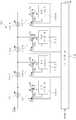
도 12에 따르면, 본 발명의 일 실시예에 따른 LED발광장치는 교류 전원(11), 정류회로부(12), 복수의 LED부(13-1내지 13-4), 복수의 스위치(14-1내지 14-4), 정전류 제어회로부(15-1내지 15-4), 전류 비교부(16), 평균 전류 제어회로부(18-1내지 18-4), 및 신호 발생부(19)를 포함한다.According to FIG. 12, the LED light emitting device according to the exemplary embodiment of the present invention includes an
교류 전원(11)은 상용 교류 전원일 수 있고, 정현파 형태로 교류 전압을 공급할 수 있다.The
정류회로부(12)는 교류 전원(11)으로부터 공급된 교류 전압을 정류함으로서 단방향 맥류 전압을 생성한다. 정류회로부(12)는 복수의 다이오드를 이용하여 구현된 브릿지 회로 일 수 있다.The
복수의 LED부(13-1내지 13-4)는 상호 직렬 연결될 수 있다. 도 12에 도시된 하나의 LED부(13-1내지 13-4)는 하나의 LED이거나, 동일 극성이 상호 연결된 복수의 LED를 포함할 수 있다. 여기서 직렬 연결되는 LED의 수는 구동회로의 효율 향상과 다단계 전류제어를 목적으로 확장시킬 수 있으며, 병렬 연결되는 LED의 수는 LED 조명 램프의 광속 증가 또는 램프의 용량 증설을 목적으로 확장할 수 있다.The plurality of LEDs 13-1 to 13-4 may be connected in series with each other. One LED unit 13-1 to 13-4 illustrated in FIG. 12 may be a single LED, or may include a plurality of LEDs having the same polarity. Here, the number of LEDs connected in series can be extended for the purpose of improving the efficiency of the driving circuit and multi-step current control, and the number of LEDs connected in parallel can be extended for the purpose of increasing the luminous flux of the LED lighting lamp or increasing the capacity of the lamp. .
설명의 편의를 위해, 서로 직렬로 연결된 복수의 LED부(13-1내지 13-4)는 연결 순서에 따라 제 1 LED부, 제 2 LED부, 제 3 LED부, 제 4 LED부로 기재하기로 한다.For convenience of description, the plurality of LED units 13-1 to 13-4 connected in series with each other will be described as a first LED unit, a second LED unit, a third LED unit, and a fourth LED unit according to a connection order. do.
각 스위치(14-1 내지 14-4)는, 복수의 LED부(13-1 내지 13-4)에 포함된 각각의 LED부가 상호 연결된 노드에 일단이 연결될 수 있다. 즉, 제 1 LED부(13-1)와 제 2 LED부(13-2)의 연결 노드에 제 1 스위치(14-1)가 연결될 수 있고, 제 2 LED부(13-2)와 제 3 LED부(13-3)의 연결 노드에 제 2 스위치(14-2)가 연결될 수 있으며, 제 3 LED부(13-3)와 제 4 LED부(13-4)의 연결 노드 사이에 제 3 스위치(14-3)가 연결될 수 있다.Each switch 14-1 to 14-4 may have one end connected to a node to which each LED unit included in the plurality of LED units 13-1 to 13-4 are interconnected. That is, the first switch 14-1 may be connected to the connection node of the first LED unit 13-1 and the second LED unit 13-2, and the second LED unit 13-2 and the third LED may be connected to each other. The second switch 14-2 may be connected to the connection node of the LED unit 13-3, and the third switch may be connected between the third LED unit 13-3 and the connection node of the fourth LED unit 13-4. The switch 14-3 may be connected.
이 스위치(14-1내지 14-4)는 후술할 전류 비교부(16)의 출력인 스위칭 제어 신호(S1내지 S4)에 따라 동작할 수 있다. 또한, 스위치(14-1내지 14-4)는 정전류 제어회로부(15-1내지 15-4)로부터 온 제어 신호에 따라 동작할 수 있다.The switches 14-1 to 14-4 may operate according to the switching control signals S1 to S4 which are outputs of the
정전류 제어회로부(15-1내지 15-4)는, 복수의 LED부(13-1내지 13-4)에 흐르는 전류가 일정한 크기를 갖도록 제어할 수 있다. 정전류 제어회로부(15-1내지 15-4)는 스위치(14-1내지 14-4)의 타단에 연결될 수 있다.The constant current control circuit units 15-1 to 15-4 can control the current flowing through the plurality of LED units 13-1 to 13-4 to have a constant magnitude. The constant current control circuit unit 15-1 to 15-4 may be connected to the other end of the switch 14-1 to 14-4.
정전류 제어회로부(15-1내지 15-4)는 스위치(14-1내지 14-4)로 구성되는 능동스위치 제어부 (10-1내지 10-4, 도 13참조)의 스위칭 제어 신호를 생성하고, 최대 전류를 제어하기 위해 제어 신호(Vgs)를 생성한다. 이에 대하여는 후술한다.The constant current control circuit unit 15-1 to 15-4 generates a switching control signal of the active switch control unit 10-1 to 10-4 (see FIG. 13) composed of the switches 14-1 to 14-4. Generate a control signal (Vgs) to control the maximum current. This will be described later.
전류 비교부(16)는 정전류 제어회로부(15-1내지 15-4)에 따라 스위치(14-2내지 14-4)를 통해 흐르는 전류들(i2내지 i4)을 수신하고, 스위치(14-1내지 14-4)의 스위칭 제어 신호(S1내지 S4)를 생성할 수 있다. 더욱 상세하게는, 전류 비교부(16)는 정전류 제어회로부(15-1내지 15-4)가 순차적으로 동작하도록, 스위치(14-1내지 14-4)의 단락(턴온) 또는 개방(턴오프) 에 따라 스위칭 제어 신호들(S1내지 S4)을 생성한다. 즉, 각 스위칭 제어 신호들(S1내지 S4)은 후단의 전류(i2내지 i4)가 수신되고, 그들 중 어느 하나라도 기설정된 값에 도달한 경우, 대응하는 스위치(14-1내지 14-4)를 개방 상태(턴오프)로 변경한다. 예를 들어, 제 1 스위칭 제어 신호(S1)는 후단의 전류(i2내지 i4)를 입력받아 그들 중 어느 한 전류가 기설정된 값에 도달한 경우, 제 1 스위치(14-1)를 개방 상태(턴오프)로 변경하고, 제 2 스위칭 제어 신호(S2)는 후단의 전류(i3내지 i4)를 입력받아 그들 중 어느 한 전류가 기설정된 값에 도달한 경우, 제 2 스위치(14-2)를 개방 상태(턴오프 상태)로 변경한다. 그리고 제 3 스위칭 제어 신호(S3)는 후단의 전류(i4)를 입력받아 대응하는 전류가 기설정된 값에 도달하면, 제 3 스위치(14-3)를 개방 상태(턴오프)로 변경한다.The
평균 전류 제어회로부(18-1내지 18-4)는 스위치(14-1내지 14-4)에 흐르는 전류의 평균값을 제어하기 위해 펄스 폭 변조(Pulse-Width Modulation, PWM) 신호를 생성한다. 평균 전류 제어회로부(18-1내지 18-4)는 교류 전원에 관계없이 정전류 제어회로부(15-1내지 15-4)의 전류를 검출하고, LED부(13-1내지 13-4)에 흐르는 구동 전류의 평균값을 제어할 수 있다. 예를 들면, 교류 전압이 통상의 전압 레벨보다 과전압인 경우, LED부(13-1 내지 13-4)의 구동 구간을 감소시키도록 PWM 신호의 듀티를 감소시켜 해당 스위치(14-1 내지 14-4)의 구동시간을 감소시킨다. 이와 반대로 교류 전압이 저전압인 경우, 상기 LED부(13-1 내지 13-4)의 구동 구간을 증가시키도록 PWM 신호의 듀티(duty)를 증가시켜 해당 스위치(14-1 내지 14-4)의 구동시간을 증가시킨다.The average current control circuit unit 18-1 to 18-4 generates a pulse-width modulation (PWM) signal to control the average value of the current flowing through the switches 14-1 to 14-4. The average current control circuit section 18-1 to 18-4 detects the current of the constant current control circuit section 15-1 to 15-4 and flows to the LED section 13-1 to 13-4 regardless of the AC power source. The average value of the drive current can be controlled. For example, when the AC voltage is overvoltage than the normal voltage level, the duty of the PWM signal is reduced so as to reduce the driving section of the LEDs 13-1 to 13-4, and the corresponding switches 14-1 to 14-. Reduce the drive time of 4). On the contrary, when the AC voltage is a low voltage, the duty of the PWM signal is increased to increase the driving period of the LEDs 13-1 to 13-4, and thus the corresponding switches 14-1 to 14-4 of the corresponding switches 14-1 to 14-4. Increase run time.
한편 상기 평균전류 제어회로부(18-1 내지 18-4)는 PWM 신호를 통하여 상기 스위치(14-1 내지 14-4)를 구동하기 때문에, 각 단에서의 LED 구동전류는 후술하는 바와 같이 펄스파 형태로 생성된다.On the other hand, since the average current control circuits 18-1 to 18-4 drive the switches 14-1 to 14-4 through PWM signals, the LED driving current at each stage is a pulse wave as will be described later. It is created in the form.
신호 발생부(19)는 PWM신호를 생성하기 위해, 램프(RAMP) 신호를 생성하고, 이것을 평균 전류 제어회로부(18-1내지 18-4)에게 가한다. 여기서, 생성된 신호의 주파수는 LED부(13-1내지 13-4)의 평균 구동 전류에 따라 결정될 수 있으며, 예를 들면, 1KHz 내지 100KHz일 수 있다.The
도 12에 도시된 본 발명의 일 실시예에 따른 교류 전원을 사용하는 LED발광장치의 동작에 대하여 상세하게 설명하도록 한다. 도 3과 관련하여 실질적으로 중복하여 기술된 본 실시예에 대한 설명은 생략하기로 한다. 도 12에 따르면, 맥류 전압은 복수의 LED부(13-1내지 13-4)에게 제공된다. 따라서, 맥류 전압이 증가하면, LED부(13-1내지 13-4)는 순차적으로 발광한다. 그러한 LED부의 발광 동작은 도 4 및 도 5와 관련하여 기술되었다.The operation of the LED light emitting device using the AC power source according to an embodiment of the present invention shown in FIG. 12 will be described in detail. Description of the present embodiment described in substantially overlapping with respect to Figure 3 will be omitted. According to FIG. 12, the pulse voltage is provided to the plurality of LED units 13-1 to 13-4. Therefore, when the pulse current voltage increases, the LEDs 13-1 to 13-4 emit light sequentially. The light emitting operation of such LED portion has been described with reference to FIGS. 4 and 5.
제 1 평균전류 제어회로부(18-1)는 제 1 정전전류 제어회로부(15-1)의 전류를 검출하고, 기준 전류와의 오차에 따른 PWM 신호를 생성하여 제 1 스위치(14-1)를 구동한다. 즉, 실제 전류가 기준 전류보다 크거나 작으면 PWM신호의 듀티는 변화된다. 따라서, 도 5에 도시된 바와 같이, 시간 구간 t0-t1에 있어서, 제 1 LED부(13-1)의 구동전류는 피크 전류가 일정하게 유지되면서 PWM 신호에 대응하는 펄스파 형태로 형성된다.The first average current control circuit unit 18-1 detects the current of the first electrostatic current control circuit unit 15-1 and generates a PWM signal according to an error from the reference current to operate the first switch 14-1. Drive. That is, the duty of the PWM signal is changed if the actual current is larger or smaller than the reference current. Therefore, as shown in FIG. 5, in the time interval t0 -t1 , the driving current of the first LED unit 13-1 is formed in a pulse wave shape corresponding to the PWM signal while the peak current is kept constant. do.
제 2 평균전류 제어회로부(18-2)는 상기 제 2 정전류 제어회로부(15-2)의 전류를 검출하고, 기준 전류와의 오차에 따른 PWM 신호를 생성하여 제 2 스위치(14-2)를 구동한다. 따라서, 도 5에 도시된 바와 같이, 시간 구간 t1-t2에 있어서, 제 1 LED부(13-1) 및 제 2 LED부(13-2)의 구동전류는 피크 전류가 일정하게 유지되면서 PWM 신호에 대응하는 펄스파 형태로 형성된다.The second average current control circuit unit 18-2 detects the current of the second constant current control circuit unit 15-2 and generates a PWM signal according to an error from the reference current to operate the second switch 14-2. Drive. Therefore, as shown in FIG. 5, in the time interval t1- t2 , the driving currents of the first LED unit 13-1 and the second LED unit 13-2 are maintained at a constant peak current. It is formed in the form of a pulse wave corresponding to the PWM signal.
제 3 평균전류 제어회로부(18-3)는 제 3 정전류 제어회로부(15-3)의 전류를 검출하고, 기준 전류와의 오차에 따른 PWM 신호를 생성하여 제 3 스위치(14-3)를 구동한다. 따라서, 도 5에 도시된 바와 같이, 시간 구간 t2-t3에 있어서, 제 1 LED부(13-1) 내지 제 3 LED부(13-3)의 구동전류는 피크전류가 일정하게 유지되면서 PWM 신호에 대응하는 펄스파 형태로 형성된다..The third average current control circuit unit 18-3 detects the current of the third constant current control circuit unit 15-3, generates a PWM signal according to an error from the reference current, and drives the third switch 14-3. do. Therefore, as shown in FIG. 5, in the time period t2 -t3 , the driving current of the first LED unit 13-1 to the third LED unit 13-3 is maintained with a constant peak current. It is formed in the form of a pulse wave corresponding to the PWM signal.
제 4 평균전류 제어회로부(18-4)는 제 4 정전류 제어회로부(15-4)의 전류를 검출하고, 기준 전류와의 오차에 따른 PWM 신호를 생성하여 제 4 스위치(14-4)를 구동한다. 따라서, 도 5에 도시된 바와 같이, 시간 구간 t3-t4에 있어서, 제 1 LED부(13-1) 내지 제 4 LED부(13-4)의 구동전류는 피크전류가 일정하게 유지되면서 PWM 신호에 대응하는 펄스파 형태로 형성된다.The fourth average current control circuit unit 18-4 detects the current of the fourth constant current control circuit unit 15-4, generates a PWM signal according to an error with the reference current, and drives the fourth switch 14-4. do. Therefore, as shown in FIG. 5, in the time interval t3- t4 , the driving current of the first LED unit 13-1 to the fourth LED unit 13-4 is maintained while the peak current is kept constant. It is formed in the form of a pulse wave corresponding to the PWM signal.
맥류 전압이 정점을 지나 점차 감소하게 되면, 제 4 LED부(13-4)에서 제 1 LED부(13-1)의 순서대로 턴오프 된다. 제 4 LED부가(13-4)가 턴오프 되면(t4 시점), 전류비교부(16)는 제 4 정전류 제어회로부(15-4)의 전류(i4)가 기설정된 값이 아님을 검출하여 제 3 스위칭 제어신호(S3)를 반전시키고, 따라서 제 3 스위치(14-3)를 단락(턴온)시킨다. 이때, 제 1 스위칭 제어신호(S1) 및 제 2 스위칭 제어신호(S2)는 이전 상태를 유지하여 제 1 스위치(14-1) 및 제 2 스위치(14-2)는 개방(턴오프)상태를 유지한다. 이와 동시에 제 3 정전류 제어부(15-3)에 전류가 입력되고 제 1 내지 제 3 LED부(13-1 내지 13-3)를 구동하도록 사전 설정된 기준 전류를 유지하도록 정전류 제어를 개시한다.When the pulse current voltage gradually decreases past the peak, it is turned off in the order of the first LED unit 13-1 from the fourth LED unit 13-4. When the fourth LED unit 13-4 is turned off (time t4 ), the
여기서, 제 3 평균전류 제어회로부(18-3)는 제 3 정전류 제어회로부(15-3)의 전류를 검출하고, 기준 전류와의 오차에 따른 PWM 신호를 생성하여 제 3 스위치(14-3)를 구동한다. 따라서, 도 5에 도시된 바와 같이, 시간 구간 t4-t5에 있어서, 제 1 LED부(13-1) 내지 제 3 LED부(13-3)의 구동전류는 피크전류가 일정하게 유지되면서 PWM 신호에 대응하는 펄스파 형태로 형성된다.Here, the third average current control circuit unit 18-3 detects the current of the third constant current control circuit unit 15-3, generates a PWM signal according to an error with the reference current, and generates the third switch 14-3. To drive. Therefore, as shown in FIG. 5, in the time interval t4- t5 , the driving current of the first LED unit 13-1 to the third LED unit 13-3 is maintained with a constant peak current. It is formed in the form of a pulse wave corresponding to the PWM signal.
이후의 전류 제어 동작은 상술한 t0내지 t3 구간 동안에 수행된 정전류 제어의 반대 순서로 진행된다. 따라서, 이에 대한 상세한 설명은 생략한다.Subsequently, the current control operation proceeds in the reverse order of the constant current control performed during the above t0 to t3 period. Therefore, detailed description thereof will be omitted.
도 13 및 도 14과 관련하여, LED구동 전류의 피크 전류와 평균 전류는 이후에 상세하게 설명한다.13 and 14, the peak current and average current of the LED driving current will be described in detail later.
도 13은 도 12에 기반한 교류 전원을 사용하는 LED발광장치의 상세 블록도이다.FIG. 13 is a detailed block diagram of an LED light emitting device using an AC power source based on FIG. 12.
도 13에서, 능동스위치 제어부(10-1내지 10-4)는 도 12의 스위치(14-1내지 14-4)에 대응하고, 스위칭 소자(Q1내지 Q4) 및 저항(Rg1내지 Rg4)을 포함한다. 그리고 정전류 제어회로부(15-1내지 15-4)의 제어 신호들은 스위칭 소자(Q1내지 Q4)의 게이트들(g1내지 g4)의 입력이 된다. 능동스위치 제어부(10-1내지 10-4)는 LED부(13-1내지 13-4)의 구동 전압(Vf1내지 Vf4)의 조건을 충족시키는 정전류를 생성한다.In FIG. 13, the active switch controller 10-1 to 10-4 corresponds to the switches 14-1 to 14-4 of FIG. 12 and includes switching elements Q1 to Q4 and resistors Rg1 to Rg4. do. The control signals of the constant current control circuits 15-1 to 15-4 are input to the gates g1 to g4 of the switching elements Q1 to Q4. The active switch controllers 10-1 to 10-4 generate a constant current that satisfies the conditions of the driving voltages Vf1 to Vf4 of the LED units 13-1 to 13-4.
정전류 제어회로부(15-1내지 15-4)는 스위칭 소자(Q1내지 Q4)의 소스들(sources, S1내지 s4)과 게이트들(gates, g1내지 g4)과 연결되어 있다. 또한, 정전류 제어회로부(15-1내지 15-4)는, FET(Field Effect Transistor) 또는 BJT(Bipolar Junction Transistor)와 같은 전력 반도체를 포함하는 스위칭 소자(Q1내지 Q4)를 선형 구간에서 제어한다. 즉, 정전류 제어회로부(15-1내지 15-4)는, LED부(13-1)의 구동 전류가 피크 전류 설정값을 충족시키도록 스위칭 소자(Q1내지 Q4)의 Vgs를 제어하는 신호를 생성한다. 이 경우, 스위칭 소자(Q1내지 Q4)는 선형 구간에서 동작한다. 특히, 각 정전류 제어회로부(15-1내지 15-4)는 각자의 스위칭 소자(Q1내지 Q4)로부터 각자의 저항들(R1내지 R4)을 경유하여 흐르는 전류를 검출하고, 검출된 전류의 양에 기반하여 각자의 스위칭 소자(Q1내지 Q4)를 제어하기 위한 제어 신호를 생성한다. 이를 위해, 각 정전류 제어회로부(15-1내지 15-4)는, 검출된 전류에 따라 선택적으로 턴온되는 스위칭 요소(미도시)를 포함할 수 있다. 이러한 스위칭 요소는 FET 또는 BJT와 같은 전력 반도체들일 수 있다. 즉, 스위칭 요소가 BJT인 경우, BJT의 베이스 단자는 각 스위칭 소자(Q1내지 Q4)의 소스(s1)에 연결되고, BJT의 콜렉터 단자는 각 스위칭 소자(Q1내지 Q4)의 게이트 단자(g1) 에 연결되고, BJT의 에미터 단자는 각자의 저항(R1내지 R4)에 연결된다.The constant current control circuit units 15-1 to 15-4 are connected to the sources of the switching elements Q1 to Q4 and the gates g1 to g4. In addition, the constant current control circuits 15-1 to 15-4 control the switching elements Q1 to Q4 including a power semiconductor such as a field effect transistor (FET) or a bipolar junction transistor (BJT) in a linear section. That is, the constant current control circuit sections 15-1 to 15-4 generate signals for controlling the Vgs of the switching elements Q1 to Q4 so that the drive current of the LED section 13-1 satisfies the peak current set value. do. In this case, the switching elements Q1 to Q4 operate in a linear period. In particular, each constant current control circuit unit 15-1 to 15-4 detects a current flowing from the respective
평균전류 제어회로부(18-1 내지 18-4)는 정전류 제어회로(15-1 내지 15-4)의 전류를 검출하는 검출저항(R1 내지 R4), 검출된 전류를 DC 전류로 변환하는 전류변환부(20-1 내지 20-4), 설정된 기준전류(Iref1 내지 Iref4)를 비교하여 에러값(출력 오차)를 출력하는 제 1 비교기(21-1 내지 21-4),및 제 1 비교기(21-1 내지 21-4)의 에러값과 신호발생부(190)의 신호(Vramp)를 비교하여 PWM 신호를 생성하는 제 2 비교기(22-1 내지 22-4)를 포함하도록 구성할 수 있다.The average current control circuits 18-1 to 18-4 are detection resistors R1 to R4 for detecting currents of the constant current control circuits 15-1 to 15-4, and current conversion for converting the detected currents to DC currents. Units 20-1 to 20-4, first comparators 21-1 to 21-4 for comparing the set reference currents Iref1 to Iref4 and outputting an error value (output error), and
여기서 검출저항(R1 내지 R4)은 정전류 제어회로부(15-1 내지 15-4)와 직렬 연결되고, 전류변환부(20-1 내지 20-4)는 검출저항(R1 내지 R4)과 정전류 제어회로부(15-1 내지 15-4)의 연결점에 연결되며, 정전류 제어회로부(15-1 내지 15-4)로부터 흐르는 전류를 평균화시켜 소정 레벨로 변화시킨다. 예컨대, 전류 변환부(20-1 내지 20-4)는 필터를 포함하여 구성될 수 있다.The detection resistors R1 to R4 are connected in series with the constant current control circuits 15-1 to 15-4, and the current converters 20-1 to 20-4 are connected to the detection resistors R1 to R4 and the constant current control circuit. Connected to the connection points of 15-1 to 15-4, the current flowing from the constant current control circuits 15-1 to 15-4 is averaged and changed to a predetermined level. For example, the current converters 20-1 to 20-4 may include a filter.
전류 변환부(20-1내지 20-4)의 출력들은 제 1 비교기(21-1내지 21-4)의 부(-)단자에 연결되고, 기준 전류들(Iref1내지 Iref4)은 제 1 비교기들(21-1내지 21-4)의 정(+)단자에 연결된다. 제 1 비교기들(21-1내지 21-4)의 출력들은 제 2 비교기들(22-1내지 22-4)의 정(+)단자에 연결되고, 신호발생기(19)의 출력(Vramp)은 제 2 비교기들(22-1내지 22-4)의 부(-)단자에 연결된다.The outputs of the current converters 20-1 to 20-4 are connected to the negative terminals of the first comparators 21-1 to 21-4, and the reference currents Iref1 to Iref4 are the first It is connected to the positive terminal of the comparators 21-1 to 21-4. The outputs of the first comparators 21-1 to 21-4 are connected to the positive terminal of the second comparators 22-1 to 22-4, and the output Vramp of the
또한 평균전류 제어회로부(18-1 내지 18-4)는 LED부(13-1 내지 13-4)의 구동전류가 설정된 평균 전류를 만족하도록 스위칭소자(Q1 내지 Q4)의 Vgs를 제어하는 신호를 생성한다. 이때, 스위칭소자(Q1 내지 Q4)는 스위칭(ON/OFF)영역에서 동작한다.Also, the average current control circuits 18-1 to 18-4 provide signals for controlling the Vgs of the switching elements Q1 to Q4 such that the drive currents of the LEDs 13-1 to 13-4 satisfy the set average current. Create At this time, the switching elements Q1 to Q4 operate in the switching (ON / OFF) region.
평균 전류 제어회로부는 도 13 및 도 14을 참조하여 상술한다.The average current control circuit unit will be described in detail with reference to FIGS. 13 and 14.
도 14는 본 발명의 일 실시예에 따른 교류 전원을 사용하는 LED발광장치의 평균 전류 제어회로부의 PWM출력 신호의 파형이다.14 is a waveform of the PWM output signal of the average current control circuit of the LED light emitting device using the AC power supply according to an embodiment of the present invention.
여기서, 평균 전류 제어회로부(18-1내지 18-4)는 개별적인 전류 구간에서 동일하기 때문에, 첫번째 구간(t0내지 t1)에서의 동작에 대해서만 서술한다.Here, since the average current control circuit sections 18-1 to 18-4 are the same in the individual current sections, only the operation in the first sections t0 to t1 will be described.
먼저, 교류 전압이 기준전압인 경우, 검출저항(R1)이 정전류 제어회로부(15-1)의 전류를 검출하면, 전류변환부(18-1)가 검출된 전류를 DC 전류로 변환하여 제 1 비교기(21-1)로 입력한다. 제 1 비교기(21-1)는 기준전류(Iref1)와 전류변환부(18-1)의 출력신호를 비교하여 그 오차에 해당하는 오차 전압 신호를 출력한다. 예를 들어, 제 1 비교기(21-1)는 전류 변환부(20-1)의 출력 신호가 기준 전류(Iref1)보다 작거나 큰 경우 오차 전압 신호를 출력할 수 있다.First, when the AC voltage is the reference voltage, when the detection resistor R1 detects the current of the constant current control circuit unit 15-1, the current conversion unit 18-1 converts the detected current into a DC current to generate a first current. Input to the comparator 21-1. The first comparator 21-1 compares the output signal of the reference current Iref1 and the current converter 18-1 and outputs an error voltage signal corresponding to the error. For example, the first comparator 21-1 may output an error voltage signal when the output signal of the current converter 20-1 is smaller or larger than the reference current Iref1.
이어서, 제 2 비교기(22-1)는 신호발생부(19)에서 입력되는 신호(Vramp)와 제 1 비교기(21-1)의 출력을 비교하여 스위칭소자(Q1)를 구동하기 위한 PWM 기준 신호를 생성한다. 도 14에 도시된 바와 같이, PWM 기준 신호는 신호발생기(19)의 발생전압(Vramp)에 대응하여 1KHz 내지 100KHz의 대역을 갖는다. 여기서, PWM 기준 신호의 듀티는 입력 전압의 증감에 따른 에너지 보상을 충분히 할 수 있도록 제 1 비교기(21-1내지 21-4)의 이득(Gain)에 의해 결정된다.Subsequently, the second comparator 22-1 compares the signal Vramp input from the
스위칭소자(Q1)는 상기 평균전류 제어회로부(18-1)의 기준 PWM 신호에 따라 온-오프 스위칭하여 LED부(13-1)의 구동전류는 일정한 듀티를 갖는 펄스형태로 형성된다.The switching element Q1 is switched on and off according to the reference PWM signal of the average current control circuit unit 18-1 so that the driving current of the LED unit 13-1 is formed in a pulse shape having a constant duty.
또한, 교류 전압이 과전압인 경우, 제 1 비교기(21-1)의 부(-)단자의 입력인, 검출 전류는 증가한다. 그리고, 제 1 비교기(21-1)의 출력은 기준 교류 전압의 신호보다 더 낮은 레벨의 신호이다. 따라서, 도 14에 도시된 바와 같이, 제 2 비교기(22-1)로 입력된 신호의 레벨은 감소하고, 제 2 비교기(22-1)는 감소된 듀티로 PWM신호를 생성한다.In addition, when the AC voltage is an overvoltage, the detection current, which is an input of the negative terminal of the first comparator 21-1, increases. The output of the first comparator 21-1 is a signal having a lower level than the signal of the reference AC voltage. Thus, as shown in FIG. 14, the level of the signal input to the second comparator 22-1 decreases, and the second comparator 22-1 generates the PWM signal with the reduced duty.
따라서, 스위칭 소자(Q1)는 감소된 듀티로 PWM신호에 따라 온-오프 스위칭하므로, LED부(13-1)의 구동 전류의 듀티는 감소하게 되고, LED부(13-1)의 구동 구간이 감소됨에 따라 평균 전류 제어를 가능한다.Therefore, since the switching element Q1 is switched on and off according to the PWM signal with the reduced duty, the duty of the driving current of the LED unit 13-1 is reduced, and the driving period of the LED unit 13-1 is reduced. As it is reduced, average current control is possible.
한편, 교류 전압이 저전압인 경우, 제 1 비교기(21-1)의 부(-)단자로 입력되는 검출전류는 감소하기 때문에 제 1 비교기(21-1)의 출력은 기준 교류 전압의 경우에 비하여 높은 레벨의 신호를 출력한다. 따라서, 도 14에 도시된 바와 같이, 제 2 비교기(22-1)로 입력되는 신호레벨이 높아지므로, 제 2 비교기(22-1)는 듀티가 증가된 PWM 신호를 생성한다.On the other hand, when the AC voltage is low, the detection current input to the negative terminal of the first comparator 21-1 decreases, so that the output of the first comparator 21-1 is lower than that of the reference AC voltage. Output a high level signal. Therefore, as shown in FIG. 14, since the signal level input to the second comparator 22-1 becomes high, the second comparator 22-1 generates a PWM signal with increased duty.
따라서, LED부(13-1)의 구동전류의 듀티도 증가하게 되고, 듀티가 증가된 PWM 신호에 따라 스위칭소자(Q1)가 온-오프 스위칭하므로 LED부(13-1)의 구동구간을 증가됨에 따라 평균전류를 제어할 수 있다.Accordingly, the duty of the driving current of the LED unit 13-1 also increases, and the driving period of the LED unit 13-1 is increased because the switching device Q1 switches on and off according to the PWM signal with increased duty. The average current can be controlled accordingly.
이와 같이, 본 발명은 평균전류 제어회로부의 PWM 신호를 통해 교류 입력전압의 변화에도 LED 구동전류를 일정한 평균전류를 갖도록 제어함으로써, LED 의 광량을 항상 일정하게 출력할 수 있는 효과가 있다.As described above, the present invention controls the LED driving current to have a constant average current even with a change in the AC input voltage through the PWM signal of the average current control circuit, so that the amount of light of the LED can be constantly output.
또한 본 발명은 BJT 또는 FET와 같은 정전류 제어소자를 선형구간 제어와 PWM 스위칭 방식을 조합한 하이브리드 방식으로 제어함으로써, 입력 전력 대비 광효율을 증가시킬 수 있어 구동회로의 손실을 개선할 수 있다.In addition, the present invention is to control the constant current control element, such as BJT or FET in a hybrid method combining the linear section control and PWM switching method, it is possible to increase the optical efficiency compared to the input power can improve the loss of the driving circuit.
도 15는 다단 PWM전류 구동에 따라 LED들에게 공급된 교류 전압 및 전류의 파형이다.15 is a waveform of AC voltage and current supplied to LEDs according to multi-stage PWM current driving.
도 15에 도시된 바와 같이, LED들의 구동 전류가 계단 형태로 형성된 경우, 교류 전압이 변동하더라도 LED구동 전류는 각 계단 구간 동안 일정한 레벨로 유지될 수 있다. 또한, 교류 입력 전압의 변화에도 불구하고, LED구동 전류는 전류 제어회로부로부터 출력된 PWM신호를 이용하여 일정한 평균 전력을 갖도록 제어될 수 있어서, LED들은 일정한 광량을 출력할 수 있다.As shown in FIG. 15, when the driving currents of the LEDs are formed in the form of steps, the LED driving current may be maintained at a constant level during each step even if the AC voltage is changed. In addition, despite the change in the AC input voltage, the LED driving current can be controlled to have a constant average power using the PWM signal output from the current control circuit section, so that the LEDs can output a constant amount of light.
그러나, PWM 신호에 의해 구동되는 스위칭 소자로 전력용 반도체 소자를 사용하며, 이러한 스위칭 소자가 고주파 대역에서 스위칭함에 따라 스위칭 소자의 턴오 또는 턴 오프 시점에서 입력전원에는 많은 노이즈를 발생시킨다. 즉, 시간에 대한 전류 변화율이 커지므로 EMI(Electromagnetic Interference, 전자기적 간섭)라 불리는 다양한 형태의 노이즈가 발생한다. 이러한 노이즈를 제거하기 위해서는 EMI 필터부를 별도로 추가하여야 하기 때문에 회로 비용이 증가하고 전원회로의 소형화 및 경량화를 저해할 수 있다.However, a power semiconductor device is used as a switching device driven by a PWM signal. As the switching device switches in a high frequency band, a lot of noise is generated in the input power supply at the time of turning on or off of the switching device. That is, since the rate of change of current with respect to time increases, various types of noises called electromagnetic interference (EMI) are generated. In order to remove such noise, an EMI filter unit must be added separately, which increases the circuit cost and can hinder the miniaturization and light weight of the power supply circuit.
이러한 문제점을 해결하기 위해, 도 16의 LED발광장치가 제안되었다.In order to solve this problem, the LED light emitting device of Figure 16 has been proposed.
도 16은 본 발명의 일 실시예에 따른 LED발광장치의 블록도이다.16 is a block diagram of an LED light emitting device according to an embodiment of the present invention.
도 17은 본 발명의 일 실시예에 따른 LED발광장치의 LED채널을 보여주는 상세한 블록도이다.17 is a detailed block diagram illustrating an LED channel of an LED light emitting device according to an embodiment of the present invention.
도 16에 따르면, 본 발명의 일 실시예에 따른 LED발광장치는 교류 전원(11), 정류회로부(12), LED채널부(100내지 nx100), 및 PWM신호 발생부(30)를 포함할 수 있다.According to FIG. 16, the LED light emitting device according to the exemplary embodiment of the present invention may include an
교류 전원(11)은 정현파 형태로 교류 전압을 공급할 수 있는 상용 교류 전원일 수 있다.The
정류회로부(12)는 교류 전원(11)으로부터 공급된 교류 전압을 정류하여 단방향 맥류 전압(Vrec)을 생성할 수 있다. 정류회로부(12)는 복수의 다이오드를 이용하여 형성된 브릿지 회로일 수 있다.The
LED 채널부(100 내지 n×100)는 병렬 연결되며, 후술하는 바와 같은 PWM 신호발생부(30)에서 입력되는 PWM 신호(PWM1 내지 PWMn)에 따라 순차적으로 동작하며, 예를 들면, LED 채널부1(100), LED 채널부2(200), …, LED 채널부n(n×100)가 순차적으로 동작한다. 여기서, 각 LED 채널부(100 내지 n×100)는 동일하게 구성되며, 도 17을 참조하여 상세히 설명한다.The
도 17에 도시된 바와 같이, 본 발명의 일 실시예에 따른 LED발광장치의 LED채널부(100)는 복수의 LED부(113-1내지 113-4), 복수의 스위치(Q1내지 Q4), 정전류 제어회로부(115-1내지 115-4), 및 전류 제어회로부(118)를 포함할 수 있다. 여기서, 비록 도면은 네개의 LED부, 네개의 스위치, 네개의 정전류 제어회로부, 및 네 개의 전류 제어회로부를 도시하고 있으나, 개수는 이에 한정되지 아니하고, 구동 회로 및 다단 전류 제어의 효율에 따라 제공될 수 있다.As shown in FIG. 17, the
LED부(113-1내지 113-4)는 직렬로 서로 연결될 수 있다. 도 17에서, 하나의 LED부(113-1내지 113-4부 중 어느 하나)는 하나의 LED일 수 있고, 복수의 LED들, 서로 상호 연결된 복수의 같은 극성의 단자를 포함할 수 있다(즉, 병렬로 연결된 LED들). 직렬 연결된 LED들의 개수는 구동 회로들의 효율을 높이고, 다단 전류 제어를 하기 위해 증가시킬 수 있으며, 병렬 연결된 LED들의 개수는 LED장치 램프의 광속을 증가시키기 위해 증가시킬 수 있다.The LED units 113-1 to 113-4 may be connected to each other in series. In FIG. 17, one LED unit 113-1 to 113-4 may be one LED, and may include a plurality of LEDs and a plurality of terminals of the same polarity interconnected to each other (ie, , LEDs connected in parallel). The number of LEDs connected in series can be increased to increase the efficiency of the driving circuits and to control the multi-stage current, and the number of LEDs connected in parallel can be increased to increase the luminous flux of the LED device lamp.
각 스위치(Q1 내지 Q4)는, 상기 복수의 LED부(113-1 내지 113-4)에 포함된 각각의 LED부가 상호 연결된 노드에 일단이 연결될 수 있다. 즉, 제 1 LED부(113-1)와 제 2 LED부(113-2)의 연결 노드에 제 1 스위치(Q1)가 연결될 수 있고, 제 2 LED부(113-2)와 제 3 LED부(113-3)의 연결 노드에 제 2 스위치(Q2)가 연결될 수 있으며, 제 3 LED부(113-3)와 제 4 LED부(113-4)의 연결 노드 사이에 제 3 스위치(Q3)가 연결될 수 있다.Each switch Q1 to Q4 may have one end connected to a node to which each of the LED units included in the plurality of LED units 113-1 to 113-4 is interconnected. That is, the first switch Q1 may be connected to the connection node of the first LED unit 113-1 and the second LED unit 113-2, and the second LED unit 113-2 and the third LED unit are connected. The second switch Q2 may be connected to the connection node of the 113-3, and the third switch Q3 is connected between the third LED unit 113-3 and the connection node of the fourth LED unit 113-4. Can be connected.
이 스위치(Q1내지 Q4)는 전류 제어회로부(118)로부터 출력된 스위치제어 신호들(S1내지 SN)에 따라 동작할 수 있다. 또한, 스위치(Q1내지 Q4)는 정전류 제어회로부(115-1내지 115-4)로부터 출력된 제어 신호에 따라 동작할 수 있다.The switches Q1 to Q4 may operate according to the switch control signals S1 to SN output from the current
정전류 제어회로부(115-1내지 115-4)는 복수의 LED부(113-1내지 113-4)를 통해 흐르는 전류가 기설정된 크기를 갖도록 제어할 수 있다. 정전류 제어회로부(115-1내지 115-4)는 스위치(Q1내지 Q4)의 타단에 연결될 수 있다.The constant current control circuits 115-1 to 115-4 may control the current flowing through the LEDs 113-1 to 113-4 to have a predetermined size. The constant current control circuits 115-1 to 115-4 may be connected to the other ends of the switches Q1 to Q4.
정전류 제어회로부(115-1내지 115-4)는 스위치(Q1내지 Q4)로서 구현되는 스위치부(10-1내지 10-4)을 위한 스위칭 제어 신호를 생성한다. 그리고, 최고 전류를 제어하기 위해 제어 신호(Vgs)를 생성한다.The constant current control circuit sections 115-1 to 115-4 generate a switching control signal for the switch sections 10-1 to 10-4 implemented as the
한편, 스위치(Q1내지 Q4)와 정전류 제어회로부(115-1내지 115-4)는 정전류 제어부(110-1 내지 110-4)를 구성한다. 더욱 상세하게 설명하자면, 정전류 제어회로부(115-1 내지 115-4)로부터 온 제어 신호들은 각 스위치 (Q1내지 Q4)의 게이트(g1내지 g4)에 입력된다. 정전류 제어부(110-1내지 110-4)는 각 LED부(113-1내지 113-4)의 구동 전압(Vf1내지 Vf4)을 충족시키는 정전류를 생성한다.On the other hand, the switches Q1 to Q4 and the constant current control circuits 115-1 to 115-4 constitute the constant current controllers 110-1 to 110-4. More specifically, the control signals from the constant current control circuits 115-1 to 115-4 are input to the gates g1 to g4 of the respective switches Q1 to Q4. The constant current controllers 110-1 to 110-4 generate a constant current satisfying the driving voltages Vf1 to Vf4 of the LEDs 113-1 to 113-4.
정전류 제어회로부(115-1 내지 115-4)는 각 스위치(Q1내지 Q4)의 소스(S1내지 s4)와 게이트(g1내지 g4)에 연결된다. 또한, 정전류 제어회로부(115-1내지 115-4)는 제어를 수행하여, FET 또는 BJT와 같은 전력반도체로 구성되는 스위치(Q1내지 Q4)가 선형 구간에서 동작하도록 한다. 즉, 정전류 제어회로부(115-1내지 115-4)는 스위치(Q1내지 Q4)를 제어하기 위한 신호(Vgs)를 생성하여, LED부(113-1내지 113-4)의 구동 전류가 기설정된 피크 전류를 충족시키도록한다.The constant current control circuits 115-1 to 115-4 are connected to the sources S1 to s4 and the gates g1 to g4 of the switches Q1 to Q4. In addition, the constant current control circuits 115-1 to 115-4 perform control so that the
상기 전류 제어회로부(118)는 상기 정전류 제어회로부(115-1 내지 115-4)에 따라 상기 스위치(Q2 내지 Q4)에 흐르는 전류를 입력 받아 상기 스위치(Q1 내지 Q4)의 스위칭 제어신호(S1 내지 S4)를 생성할 수 있다. 보다 상세하게는 상기 전류 제어회로부(118)는 상기 스위치(Q1 내지 Q4)의 단락(턴온) 또는 개방상태(턴오프)에 따라 상기 정전류 제어회로부(115-1 내지 115-4)가 순차적으로 동작하도록 스위칭 제어신호(S1 내지 S4)를 생성한다. 즉, 전류 제어회로부(118)는 정전류 제어회로부 (115-2 내지 115-4)로부터 각 스위칭 제어신호(S1 내지 S4)는 후단의 정전류제어회로부(115-2 내지 115-4)의 전류을 입력 받아 어느 하나의 전류가 기설정된 값이 되면 해당 스위치(S1 내지 S4)를 개방상태(턴오프)로 전환한다. 예를 들면, 제 1 스위칭 제어신호(S1)에 대하여, 전류 제어회로부(118)는 후단의 정전류제어회로부(115-2 내지 115-4)의 전류를 입력 받아 어느 하나의 전류가 기설정된 값이 되면 제 1 스위치(Q1)를 개방상태로 전환시키고, 제 2 스위칭 제어신호(S2)에 대하여, 전류 제어회로부(118)는 후단의 정전류제어회로부(115-3 및 115-4)의 전류를 입력 받아 어느 하나의 전류가 기설정된 값이 되면 제 2 스위치(Q2)를 개방상태(턴오프)로 전환시키며, 제 3 스위칭 제어신호(S3)에 대하여, 전류 제어회로부(118)는 후단의 정전류제어회로부(115-4)의 전류를 입력 받아 해당 전류가 기설정된 값이 되면 제 3 스위치(Q3)를 개방상태(턴오프)로 전환시킨다The
또한, 전류 제어회로부(118)는 스위치(Q1 내지 Q4)에 흐르는 전류의 평균값을 제어하기 위한 PWM 신호를 생성한다. 이러한 전류 제어회로부(118)는 교류 전원과 무관하게 정전류제어회로부(115-1 내지 115-4)의 전류를 검출하여 LED부(113-1 내지 113-4)에 흐르는 구동전류의 평균값을 제어할 수 있다. 예를 들면, 교류 전압이 통상의 전압 레벨보다 과전압인 경우, LED부(113-1 내지 113-4)의 구동 구간을 감소시키도록 PWM 신호의 듀티(duty)를 감소시켜 해당 스위치(Q1 내지 Q4)의 구동시간을 감소시킨다. 이와 반대로 교류 전압이 저전압인 경우, LED부(113-1 내지 113-4)의 구동 구간을 증가시키도록 PWM 신호의 듀티(duty)를 증가시켜 해당 스위치(Q1 내지 Q4)의 구동시간을 증가시킨다.In addition, the current
한편 전류 제어회로부(118)는 PWM 신호를 통하여 스위치(Q1 내지 Q4)를 구동하기 때문에, 각 단에서의 LED 구동전류는 펄스파 형태로 생성된다. 즉, 전류 제어회로부(118)는 각 LED부(113-1 내지 113-4)의 구동전류가 설정된 평균 전류를 만족하도록 스위치(Q1 내지 Q4)의 Vgs를 제어하는 신호를 생성한다. 이때, 스위치(Q1 내지 Q4)는 스위칭(ON/OFF)영역에서 동작하여 각 LED부(113-1 내지 113-4)의 구동전류는 일정한 듀티를 갖는 펄스형태로 형성된다.On the other hand, since the current
PWM 신호발생부(30)는 교류 전원(11)의 주파수를 검출하는 주파수 검출부(31), 검출된 주파수와 다른 기준주파수로 발진하는 기준주파수 발진회로(32), 기준 주파수를 분주하는 주파수 분주회로(33), 및 주파수 분주신호를 이용하여 PWM출력을 결정하는 PWM 출력 결정부(34)를 포함하여 구성할 수 있다.The
주파수 검출부(31)는 교류 전원(11)의 영점을 검출(zero crossing detecting)하여 구형파 신호를 생성하고, 기준 주파수 발진회로(32)는 생성된 구형파와 동기된 PWM 주파수의 기준 신호를 생성한다. 여기서 발진 신호의 주파수는 다양하게 설정될 수 있다. 주파수 분주회로(33)는 기준 PWM 주파수 신호를 정수배로 분주한다. 이와 같이 분주된 신호는 듀티가 50%로서 온/오프의 시간 비율이 1인 클럭 펄스에 의해서 Fs/n의 정수로 분주된다. 여기서 분주된 신호가 PWM 출력 결정부(34)의 기준 신호가 되며, PWM 출력 결정부(34)는 채널 수에 대응하는 n개의 PWM 결정신호(PWM1 내지 PWMn)를 생성하는데, 도 18을 참조하여 상세히 설명한다.The
도 18은 본 발명의 일 실시예에 따른 LED발광장치에서, 주파수 분주에 의한 PWM결정 신호의 파형이다.18 is a waveform of a PWM determination signal by frequency division in an LED light emitting device according to an embodiment of the present invention.
도 18에 도시된 바와 같이, PWM출력 결정부(34)는 기준 PWM주파수 신호(Fs), 및 2 분주 신호(Fs/2)를 이용하여 n개의 PWM결정 신호(PWM1내지 PWMn)를 출력한다. 즉, PWM출력 결정부(34)는 기준 신호(Fs)와 분주된 신호(Fs/2)의 논리식을 통하여 n개의 채널을 조합하고, PWM결정 신호를 생성한다. 예를 들어, 네개의 PWM결정 신호들(PWM1내지 PWM4)이 생성되면, 제 1 PWM결정 신호(PWM1)는 부정(NOT) 연산된 기준 신호(Fs) 및 2 분주된 신호(Fs/2)에 논리합(OR)연산을 수행함으로서 생성될 수 있고, 제 2 PWM결정 신호(PWM2)는 반전된 기준 신호(Fs) 및 반전된 2 분주된 신호(Fs/2)에 논리합(OR) 연산을 수행함으로서 생성될 수 있고, 제 3 PWM결정 신호(PWM3)는 기준 신호(Fs)이고, 제 4 PWM결정 신호(PWM4)는 논리적 부정(NOT) 연산을 기준 신호(Fs)에 수행함으로서 생성될 수 있다. 그러므로, PWM결정 신호(PWM1내지 PWM4)는 일부 구간이 반복적으로 중복되는 펄스의 형태를 갖는다. 즉, 도 18에서, 첫번째 구간에서 제 1 PWM 결정신호(PWM1)와 제 3 PWM 결정신호(PWM3)가 중복되고, 제 2 구간에서 제 1 PWM 결정신호(PWM1), 제 2 PWM 결정신호(PWM2) 및 제 4 PWM 결정신호(PWM4)가 중복되며, 세번째 구간에서 제 2 PWM 결정신호(PWM2)와 제 3 PWM 결정신호(PWM3)가 중복되고, 네번째 구간에서 제 1 PWM 결정신호(PWM1), 제 2 PWM 결정신호(PWM2) 및 제 4 PWM 결정신호(PWM1)가 중복된다.As illustrated in FIG. 18, the
도 15에 따른 본 발명의 일 실시예에 따른 교류 전원을 사용하는 LED발광장치의 동작에 대해 이하에서 상세하게 설명한다.The operation of the LED light emitting device using the AC power source according to the embodiment of the present invention according to FIG. 15 will be described in detail below.
이하, 본 발명의 일 실시예에 따른 도 16 및 17에 도시된 교류 전원을 사용하는 LED발광장치의 동작에 대해서 설명한다.Hereinafter, the operation of the LED light emitting device using the AC power source shown in Figures 16 and 17 according to an embodiment of the present invention.
먼저, 교류 전원(11)에 의해 교류 전압이 정류회로부(12)로 입력되면, 정류회로부(12)는 이를 정류하여 단방향을 갖는 맥류 전압(Vrec)을 출력한다. 도 15에 도시된 것과 같이, 교류 전원(11)의 출력전압, 즉 정류회로부(12)로 입력되는 전압은 정의 방향과 부의 방향을 모두 갖는 교류 전압이며, 정류회로부(12)에서 출력되는 전압은 부의 방향의 전압을 정의 방향으로 변환한 단 방향의 맥류 전압(Vrec)의 형태를 갖는다. 이러한 맥류 전압(Vrec)은 다수의 상기 LED 채널부(100 내지 n×100)에 제공된다. 이하에서는 LED 채널부(100 내지 n×100)의 동작이 동일하므로 LED 채널부1(100)을 중심으로 설명한다.First, when an AC voltage is input to the
LED 채널부1(100)에 입력되는 맥류 전압(Vrec)이 증가함에 따라, LED부(113-1 내지 113-4)가 순차적으로 발광될 수 있다. 이러한 LED부의 발광동작은 도 4 및 도 5을 함께 참조하여 설명하기로 한다.As the pulse current voltage Vrec input to the
도 4는 본 발명의 일 실시예에 따른 LED발광장치의 LED들에게 공급된 교류 전압과 교류 전류의 파형이다.4 is a waveform of an AC voltage and an AC current supplied to the LEDs of the LED light emitting device according to the embodiment of the present invention.
도 5는 본 발명의 일 실시예에 따른, LED발광장치에서 공급된 스위치의 제어 신호들의 파형, 스위치를 통해 흐르는 전류의 파형, 및 LED들에게 계속적으로 공급된 전류의 파형이다.5 is a waveform of the control signals of the switch supplied from the LED light emitting device, the waveform of the current flowing through the switch, and the waveform of the current continuously supplied to the LED according to an embodiment of the present invention.
또한, 도 4 및 도 5는 정류회로부(11)에 의해 공급된 맥류 전압(Vrec)의 한 주기에 대해서만 설명하기로 한다. 이러한 이유는 맥류 전압(Vrec)의 나머지 주기에서 동일한 동작이 수행되기 때문이다.4 and 5, only one cycle of the pulse current voltage Vrec supplied by the
LED부(113-1 내지 113-4) 측으로 제공되는 맥류 전압(Vrec)의 크기가 증가하여, 제 1 LED부(113-1)의 구동 전압(순방향 전압: Vf1)이 되면, 제 1 LED부(113-1)에 전류가 흘러 발광된다(도 4 및 도 5의 t0 시점). 여기서, 제 1 스위치(Q1) 내지 제 4 스위치(Q4)는 초기에 단락(턴온) 상태로 설정된다. 이러한 입력전압(Vf1)에 대응하는 전류는 제 1 LED부(113-1)를 통하여 제 1 정전류 회로제어부(115-1)로의 경로를 따라 흐른다. 이때, 제 1 스위치(Q1)는 제 1 정전류 제어회로부(115-1)의 제어신호에 따라 제 1 정전류 제어회로부(115-1)를 통과하는 전류를 일정하게 제어한다. 제 1 정전류 제어회로부(115-1)는 제 1 LED부(113-1)를 구동하도록 기설정된 전류가 흐를 수 있도록 정전류 제어한다. 이와 같은 제 1 LED부(113-1)가 발광이 개시되는 동작은 시간 구간 t0-t1에 해당한다. 여기서, 전류 제어회로부(118)는 제 1 정전류 제어회로부(115-1)의 전류를 검출하고, 기준 전류와의 오차에 따른 PWM 신호를 생성하여 제 1 스위치(Q1)를 구동한다.When the magnitude of the pulse current voltage Vrec provided to the LED parts 113-1 to 113-4 increases to become the driving voltage (forward voltage Vf1) of the first LED part 113-1, the first LED part Current flows to 113-1 to emit light (time t0 in FIGS. 4 and 5). Here, the first switch Q1 to the fourth switch Q4 are initially set to a short circuit (turn on) state. The current corresponding to the input voltage Vf1 flows along the path to the first constant current circuit control unit 115-1 through the first LED unit 113-1. At this time, the first switch Q1 constantly controls the current passing through the first constant current control circuit unit 115-1 according to the control signal of the first constant current control circuit unit 115-1. The first constant current control circuit unit 115-1 controls the constant current so that a predetermined current flows to drive the first LED unit 113-1. The operation of starting light emission of the first LED unit 113-1 corresponds to a time interval t0 -t1 . Here, the current
이 경우, PWM출력 결정부(34)에 의해 생성된 PWM결정 신호(PWM1내지 PWMn)에 따라, 각 LED채널부(100내지 400)는 순차적으로 동작될 수 있다. 즉, 도 5에 도시된 바와 같이, LED채널부(100내지 400)는 PWM결정 신호(PWM1내지 PWM4)에 따라 순차적으로 구동되고, 이로 인해 각 LED채널부(100내지 400)의 제 1 LED부(113-1)는 순차적으로 턴온된다. 여기서, PWM결정 신호(PWM1내지 PWM4)는 일정 구간 중복되기 때문에, LED채널부(100내지 400)의 제 1 LED부(113-1)가 동시에 턴온된 경우, 두 개 또는 세 개의 LED채널부(100내지 400)가 몇몇 구간에서 동시에 구동되고, 결국, LED구동 전류는 직류 레벨로 시프트된 전류의 형태로 생성된다.In this case, according to the PWM determination signals PWM1 to PWMn generated by the PWM
다음으로, 맥류 전압(Vrec)의 크기가 더 증가하여, 제 2 LED부(113-2)에 인가된 전압이 제 2 LED(113-2)의 구동 전압이 된때(맥류 전압(Vrec)의 크기가 Vf2가 된때), 전류가 제 2 LED부(113-2)를 통해 흘러 발광한다(도 4 및 도 5의 t1시점). 여기서, 입력 전압(Vf2)에 대응하는 전류는 제 2 LED(113-2)를 통해 제 2 정전류 제어회로부(115-2)로 가는 경로를 통해 흐른다. 이 경우, 전류 제어회로부(118)는 제 2 정전류 제어회로부(115-2)의 전류가 기설정된 값인지 검출하고, 제 1 스위칭 제어 신호(S1)를 생성하고, 제 1 스위치(Q1)를 개방한다(턴오프). 동시에, 제 2 정전류 제어회로부(115-2)로부터의 제어신호에 따라 제 2 스위치(Q2)는 제 2 정전류 제어회로부(115-2)에 흐르는 전류가 제 1 LED부(113-1) 및 제 2 LED부(113-2)를 구동하기 위해 기설정된 전류가 되도록 제어를 수행한다.Next, when the magnitude of the pulse voltage Vrec increases further, when the voltage applied to the second LED unit 113-2 becomes the driving voltage of the second LED 113-2 (of the pulse voltage Vrec). When the magnitude becomes Vf2), a current flows through the second LED portion 113-2 to emit light (time t1 in FIGS. 4 and 5). Here, the current corresponding to the input voltage Vf2 flows through the path to the second constant current control circuit unit 115-2 through the second LED 113-2. In this case, the current
이러한 동작을 통해, 일정한 전류가 제 1 LED부(113-1)와 제 2 LED부(113-2)를 통해 흐르도록 제어가 수행될 수 있다. 또한, 도 4 및 도 5에 도시된 바와 같이, t1시점에, 제 1 스위치(Q1)가 턴오프되며, 제 2 정전류 제어회로부(115-1)에 의해 수행된 정전류 제어를 이용하여 계단 입력 전류가 형성될 수 있다. 여기서, 전류 제어회로부(118)는 제 2 정전류 제어회로부(115-2)의 전류를 검출하고, 검출된 전류와 기준 전류 간의 오차에 따라 PWM신호를 생성하고, 제 2 스위치(Q2)를 구동한다. 따라서, 도 5에 도시된 바와 같이, 시간 구간 t1-t2에서, LED채널부(100내지 400)는 PWM결정 신호(PWM1내지 PWM4)에 따라 순차적으로 구동되고, LED채널부(100내지 400)의 제 1 LED부(113-1)와 제 2 LED부(113-2)는 턴온된다. 여기서, PWM 결정신호(PWM1 내지 PWM4)는 일정 구간 중복되기 때문에, 구간에 따라 LED 채널부(100 내지 400) 중 두 개 또는 세 개가 동시 구동되며 이때, 해당 LED 채널부(100 내지 400)의 제 1 LED부(113-1) 및 제 2 LED부(113-2)가 동시에 턴온되고, 결과적으로 LED 구동 전류는 직류 레벨 시프트된 전류 형태로 형성된다.Through this operation, control may be performed such that a constant current flows through the first LED unit 113-1 and the second LED unit 113-2. 4 and 5, at time t1 , the first switch Q1 is turned off and the stair input is performed by using the constant current control performed by the second constant current control circuit 115-1. Current can be formed. Here, the current
상술한 바와 같이, 맥류 전압(Vrec)이 더 증가하고, 제 3 LED부(113-3)에 인가되는 전압이 제 3 LED부(113-3)의 구동 전압이 된 경우(맥류 전압 (Vrec)의 크기가 Vf3이 된 경우), 전류가 제 3 LED부(113-3)에 흘러 발광된다(도 4 및 도 5의 t2시점). 이 경우, 입력 전압(Vf3)에 대응하는 전류는 제 3 LED(113-3)를 통해 제 3 정전류 제어회로부(115-3)로 가는 경로를 통해 흐른다. 여기서, 전류 제어회로부(118)는 제 3 정전류 제어회로부(115-3)가 기설정된 값을 갖는지 검출하고, 제 2스위칭 제어 신호(S2)를 생성하고, 제 2스위치(Q2)를 개방한다(턴오프). 제 1 스위칭 제어 신호(S1)가 예전 상태를 유지하여 제 1 스위치(Q1)가 개방 상태(턴오프)로 유지된다. 동시에, 제 3 정전류 제어회로부(115-3)로부터 온 제어 신호에 따라, 제 3 스위치(Q3)는 제 3 정전류 제어회로부(115-3)를 통해 흐르는 전류가 제 1 LED부(113-1) 내지 제 3 LED부(113-3)를 구동하도록 기설정된 전류가 되도록 제어를 수행한다.As described above, when the pulse voltage Vrec further increases, and the voltage applied to the third LED part 113-3 becomes the driving voltage of the third LED part 113-3 (pulse voltage Vrec) If the size of the Vf3), the light emission current is flowing to the LED unit 3 (113-3) (Fig. 4 and the time t2 in Fig. 5). In this case, a current corresponding to the input voltage Vf3 flows through the path to the third constant current control circuit unit 115-3 through the third LED 113-3. Here, the current
이러한 동작을 이용하여, 제 1 LED부(113-1), 제 2 LED부(113-2), 및 제 3 LED부(113-3)를 통해 일정한 전류가 흐르도록 제어가 수행된다. 또한, 도 4 및 도 5에 도시된 바와 같이, t2시점에, 제 1 스위치(Q1) 및 제 2 스위치(Q2)는 턴오프되고, 계단 입력 전류는 제 3 정전류 제어회로부(115-3)에 의해 수행된 정전류 제어를 이용해 형성될 수 있다. 여기서 전류 제어회로부(118)는 제 3 정전류 제어회로부(115-3)의 전류를 검출하고, 검출된 전류 및 기준 전류 간의 오차에 따라 PWM신호를 생성하고, 제 3 스위치(Q3)를 구동한다. 따라서, 도 4에 도시된 바와 같이, 시간 구간 t2-t3동안, LED채널부(100내지 400)는 턴온된다. 여기서, PWM결정 신호들(PWM1내지 PWM4)는 일정 구간 중복되기 때문에, 제 1 내지 제 3 LED부(113-1내지 113-3)가 동시에 턴온되는 경우, 두개 또는 세개의 LED채널부(100내지 400)는 몇몇 구간에서 동시에 구동된다. 따라서, LED구동 전류는 직류 레벨로 시프트된 전류 형태로 생성된다.Using this operation, control is performed such that a constant current flows through the first LED unit 113-1, the second LED unit 113-2, and the third LED unit 113-3. 4 and 5, at time t2 , the first switch Q1 and the second switch Q2 are turned off, and the step input current is the third constant current control circuit unit 115-3. It can be formed using the constant current control performed by. The current
상술한 바와 유사하게, 맥류 전압(Vrec)이 더 증가하고, 제 4 LED부(113-4)로 인가된 전압이 제 4 LED부(113-4)의 구동 전압이 된 경우(맥류 전압(Vrec)의 크기가 Vf4가 된 경우), 전류가 제 4 LED부(113-4)를 통해 흘러, 발광된다(도 4 및 도 5의 t3시점에서). 이 경우, 입력 전압(Vf4)에 대응하는 전류는 또한, 제 4 LED(113-4)를 경유하여, 제 4 정전류 제어회로부(115-4)로 가는 경로를 통해 흐른다. 여기서, 전류 제어회로부(118)는 제 4 정전류 제어회로부(115-4)가 기설정된 값을 갖는지 검출하고, 제 3 스위칭 제어 신호(S3)를 생성하고, 제 3 스위치(Q3)를 개방한다(턴오프). 제 1 및 제 2 스위칭 제어 신호(S1 및 S2)는 이전의 상태를 유지하여, 제 1 및 제 2 스위치(Q1 및 Q2)가 개방 상태(턴오프)로 유지 되도록 한다. 동시에, 네번째 정전류 제어회로부(115-4)의 제어 신호에 따라 제 4 스위치(Q4)는 제 4 정전류 제어회로부(115-4)를 통해 흐르는 전류가 제 1 내지 제 4 LED부(113-1내지 113-4)를 구동하도록 기설정된 전류가 되게하도록 제어를 수행한다.Similarly to the above, when the pulse voltage Vrec increases further and the voltage applied to the fourth LED part 113-4 becomes the driving voltage of the fourth LED part 113-4 (pulse voltage Vrec ) Becomes Vf4), a current flows through the fourth LED section 113-4, and emits light (at the time t3 in FIGS. 4 and 5). In this case, the current corresponding to the input voltage Vf4 also flows through the path to the fourth constant current control circuit section 115-4 via the fourth LED 113-4. Here, the current
이러한 동작을 이용하여, 일정한 전류가 제 1 LED부(113-1), 제 2 LED부(113-2), 제 3 LED부(113-3), 및 제 4 LED부(113-4)를 통해 흐르도록 제어는 수행된다. 또한, 도 4 및 도 5에 도시된 바와 같이, t3시점에 제 3 스위치는 꺼지고, 계단 입력 전류는 제 4 정전류 제어회로부(115-4)에 의한 정전류 제어를 이용해 형성될 수 있다. 여기서, 전류 제어회로부(118)는 제 4 정전류 제어회로부(115-4)의 전류를 검출하고, 검출된 전류와 기준 전류 간의 오차에 의존하는 PWM신호를 생성하고, 제 4 스위치(Q4)를 구동한다. 따라서, 도 5에 도시된 바와 같이, t3-t4구간에서, LED채널부(100내지 400)는 PWM결정 신호(PWM1내지 PWM4)에 따라 순차적으로 구동되어, LED채널부(100내지 400)의 제 1 LED부(113-1) 내지 제 4 LED부(113-4)는 턴온된다. 여기서, PWM결정 신호(PWM1내지 PWM4)는 일정 구간에서 중복되기 때문에, LED채널부(100내지 400)의 제 1 내지 제 4 LED부(113-1내지 113-4)가 동시에 턴온되면, 두 개 또는 세 개의 LED채널부(100내지 400)는 몇몇 구간에서 동시에 구동된다. 결국, LED구동 전류는 직류 레벨로 전환된 시프트된 형태로 생성된다.Using this operation, a constant current is applied to the first LED unit 113-1, the second LED unit 113-2, the third LED unit 113-3, and the fourth LED unit 113-4. Control is performed to flow through. 4 and 5, the third switch is turned off at time t3 , and the staircase input current may be formed using the constant current control by the fourth constant current control circuit 115-4. Here, the current
맥류 전압(Vrec)이 피크를 지나 점차 감소하게 되면, 제 4 LED부(113-4)에서 제 1 LED부(113-1)의 순서대로 턴오프 된다. 제 4 LED부(113-4)가 턴오프 되면(t4시점), 상기 전류 제어회로부(118)는 제 4 정전류 제어회로부(115-4)의 전류가 기설정된 값이 아님을 검출하여 제 3 스위칭 제어신호(S3)을 반전시키고, 따라서 제 3 스위치(Q3)를 단락(턴온)시킨다. 이때, 제 1 스위칭 제어신호(S1) 및 제 2 스위칭 제어신호(S2)는 이전 상태를 유지하여 제 1 스위치(Q1) 및 제 2 스위치(Q2)는 개방(턴오프)상태를 유지한다. 이와 동시에 제 3 정전류 제어회로부(115-3)에 전류가 입력되고 제 1 내지 제 3 LED부(113-1 내지 113-3)를 구동하기 위한 정전류 제어가 개시되어 기설정된 전류가 유지된다.When the pulse voltage Vrec gradually decreases past the peak, the pulse voltage Vrec is turned off in the order of the first LED unit 113-1 from the fourth LED unit 113-4. When the fourth LED unit 113-4 is turned off (t4 Time point), the current
여기서, 전류 제어회로부(118)는 제 3 정전류 제어회로부(115-3)의 전류를 검출하고, 기준 전류와의 오차에 따른 PWM 신호를 생성하여 제 3 스위치(Q3)를 구동한다. 따라서, 도 5에 도시된 바와 같이, 시간 구간 t4-t5에 있어서, PWM 결정신호(PWM1 내지 PWM4)에 따라 각 LED 채널부(100 내지 400)가 순차적으로 구동되며, 이에 따라 해당 LED 채널부(100 내지 400)의 제 1 LED부(113-1) 내지 제 3 LED부(113-3)가 턴온된다. 여기서, PWM 결정신호(PWM1 내지 PWM4)는 일정 구간 중복되기 때문에, 구간에 따라 LED 채널부(100 내지 400) 중 두개 또는 세개가 동시 구동하며 이때, 해당 LED 채널부(100 내지 400)의 제 1 LED부(113-1) 내지 제 4 LED부(113-4)가 동시에 턴온되고, 결과적으로 LED 구동 전류는 직류 레벨 시프트된 전류 형태로 형성된다.Here, the current
그 후의 상술한 t0-t3구간 동안의 전류 제어 동작은 정전류 제어의 반대 순서로 수행된다. 따라서, 이에 대한 상세한 설명은 생략한다.Thereafter, the current control operation during the aforementioned t0 -t3 period is performed in the reverse order of the constant current control. Therefore, detailed description thereof will be omitted.
본 발명의 일 실시예가 다단 정전류 제어를 통하여 LED규동 전류가 계단 형태로 증가하거나 감소하도록 상술되었어도, 본 발명은 이에 제한되지 아니하고, LED구동 전류의 파형도 변할 수 있도록 정전류 제어를 위한 기준 전류는 다양한 형태로 설정될 수 있다.Although an embodiment of the present invention has been described above to increase or decrease the LED driving current in a stepped form through the multi-stage constant current control, the present invention is not limited thereto, and the reference current for the constant current control may vary in order to change the waveform of the LED driving current. It can be set in the form.
이하, 도 19 및 도 20을 참조하여 LED구동 전류의 피크 전류 제어와 평균 전류 제어가 상세히 설명된다.Hereinafter, the peak current control and the average current control of the LED driving current will be described in detail with reference to FIGS. 19 and 20.
도 19는 본 발명의 일 실시예에 따라 LED발광장치에서의 PWM제어를 보여주는 상세한 블록도이다.19 is a detailed block diagram illustrating PWM control in an LED light emitting device according to an embodiment of the present invention.
도 20은 본 발명의 일 실시예에 따라 LED발광장치에서 PWM출력 신호들에 의존하는 LED구동 전류의 파형이다.20 is a waveform of an LED driving current depending on PWM output signals in an LED light emitting device according to an embodiment of the present invention.
PWM 결정신호(PWM1 내지 PWMn)에 의해 각 LED 채널부(100 내지 400)가 순차적으로 동작함으로써, LED 구동전류가 일정 구간 중복되는 전류형태를 형성하는 것을 설명하기 위하여, 도 19는 PWM 결정신호(PWM1 내지 PWM4)를 중심으로 각 LED 채널부(100 내지 400)의 첫단에 구성되는 제 1 LED부(113-1 내지 413-1)를 도시한 것이다.In order to explain that each
도 19에 도시된 바와 같이, 정류된 맥류 전압(Vrec)이 제 1 LED부(113-1내지 413-1)의 구동 전압(Vf1)이 되면, 각 LED채널부(100내지 400)의 제 1 LED부(113-1내지 413-1)는 구동된다.As shown in FIG. 19, when the rectified pulse current voltage Vrec becomes the driving voltage Vf1 of the first LED units 113-1 to 413-1, the first of each
이 경우, PWM출력 결정부(34)는 도 18에 도시된 바와 같이, PMW결정 신호(PWM1내지 PWM4)를 생성하고, 이들을 각각 전류 제어회로부(118내지 418)로 공급한다. LED채널부(100내지 400)의 전류 제어회로부(118내지 418)는 PWM결정 신호들(PWM1내지 PWM4)에 따라 순차적으로 동작한다.In this case, the
즉, 도 19에 도시된 바와 같이, 제 1 LED채널부(100)는 제 1 PWM결정 신호(PWM1)에 따라 구동된다. 제 1 LED채널부(100)의 전류 제어회로부(118-1)는 스위칭 제어 신호(S1)를 출력하여, 제 1 LED부(113-1)가 정전류 제어부(110-1)를 통해 발광하도록 한다. 즉, LED구동 전류(Ch1)는 제 1 PWM결정 신호(PWM1)에 따라 제 1 LED채널부(100)에 의해 형성된다. 여기서, 제 1 LED채널부(100)의 LED구동 전류(Ch1)는 제 1 PWM결정 신호(PWM1)와 같은 패턴으로 형성되는데, 예를 들어, 2 분주 신호(Fs/2)의 한 주기를 구성하는 네개의 구간동안 세번째 구간에서는 흐르지 않는다.That is, as shown in FIG. 19, the first
이어서, 제 2 LED채널부(200)는 제 2 PWM결정 신호(PWM2)에 따라 구동된다. 제 2 LED채널부(200)의 전류 제어회로부(218-1)가 스위칭 제어 신호(S1)를 출력하여, 제 2 LED부(213-1)가 정전류 제어부(210-1)를 통해 발광한다. 즉, LED구동 전류(Ch2)는 제 2 PWM결정 신호(PWM2)에 따라 제 2 LED채널부(200)에 의해 형성된다. 여기서, 제 2 LED채널부(200)의 LED구동 전류(Ch2)는 제 2 PWM결정 신호(PWM2)와 같은 패턴으로 형성되는데, 예를 들어, 2 분주 신호(Fs/2)의 한 주기를 구성하는 네개의 구간동안 첫번째 구간에서는 흐르지 않는다.Subsequently, the second
이어서, 제 3 LED채널부(300)은 제 3 PWM결정 신호(PWM3)에 따라 구동된다. 제 3 LED채널부(300)의 전류 제어회로부(318-1)가 스위칭 제어 신호(S1)를 출력하여, 제 3 LED부(313-1)가 정전류 제어부(310-1)를 통해 발광한다. 즉, LED구동 전류(Ch3)는 제 3 PWM결정 신호(PWM3)에 따라 제 3 LED채널부(300)에 의해 형성된다. 여기서, 제 3 LED채널부(300)의 LED구동 전류(Ch3)는 제 3 PWM결정 신호(PWM3)와 같은 패턴으로 형성되고, 예를 들어, 2 분주 신호(Fs/2)의 한 주기를 구성하는 네개의 구간동안 두번째 및 네번째 구간에서는 흐르지 않는다.Subsequently, the third
마지막으로, 제 4 LED채널부(400)는 제 4 PWM결정 신호(PWM4)에 따라 구동된다. 제 4 LED채널부(400)의 전류 제어회로부(318-1)가 스위칭 제어 신호(S1)를 출력하여, 제 4 LED부(413-1)가 정전류 제어부(310-1)를 통해 발광한다. 즉, LED구동 전류(Ch4)는 제 4 PWM결정 신호(PWM4)에 따라 제 4 LED채널부(400)에 의해 형성된다. 여기서, 제 4 LED채널부(400)의 LED구동 전류(Ch4)는 제 4 PWM결정 신호(PWM4)와 같은 패턴으로 형성되고, 예를 들어, 2 분주 신호(Fs/2)의 한 주기를 구성하는 네개의 구간동안 첫번째 및 세번째 구간에서는 흐르지 않는다.Finally, the fourth
결국, LED채널부(100내지 400)가 PWM결정 신호들(PWM1내지 PWM4)에 따라 순차적으로 구동되기 때문에, LED채널부(100내지 400)의 제 1 LED부(113-1내지 413-1)의 구동 전류를 합한 총 LED구동 전류(ILED)는 일정 구간이 반복적으로 중복되는 직류 레벨 시프트된 펄스파 형태를 형성한다. 즉, 도 20에서, 2 분주된 신호(Fs/2)의 한 주기를 구성하는 네개의 구간동안, 첫번째 구간에서는, 제 1 LED채널부(100)의 구동 전류(CH1) 및 제 3 LED채널부(300)의 구동 전류(Ch3)는 중복되고, 두번째 구간에서는, 제 1 LED채널부(100)의 구동 전류(CH1), 제 2 LED채널부(200)의 구동 전류(Ch2), 및 제 4 LED채널부(400)의 구동 전류(Ch4)는 중복되고, 세번째 구간에서는, 제 2 LED채널부(200)의 구동 전류(Ch2) 및 제 3 LED채널부(300)의 구동 전류(Ch3)는 중복되고, 네번째 구간에서는, 제 1 LED채널부(100)의 구동 전류(CH1), 제 2 LED채널부(200)의 구동 전류(Ch2), 및 제 4 LED채널부(400)의 구동 전류(Ch4)는 중복된다.As a result, since the
도 21은 본 발명의 일 실시예에 따른 LED발광장치의 블록도이다.21 is a block diagram of an LED light emitting device according to an embodiment of the present invention.
도 22A 및 도 22B는 본 발명의 일 실시예에 따른 LED발광장치에서, 개선된 LED오프 구간이 있을 때와 없을 때 각각의 LED구동 전류의 파형이다.22A and 22B are waveforms of respective LED driving currents with and without an improved LED off period in the LED light emitting device according to one embodiment of the present invention.
도 21은 오직 제 1 LED채널부(100)만 도시하고 있으나, 각 LED채널부(100내지 400)는, PWM결정 신호들(PWM1내지 PWM4)에 따라 동작될 수 있도록, 같은 구성을 갖는다.FIG. 21 shows only the first
도 21에서 본 발명의 일 실시예에 따른 LED발광장치는 도 19에 관하여 상술한 본 발명의 실시예와 같기 때문에, LED부(113-1내지 113-4)에 병렬로 연결되고, 정전류 제어부(110-5)에 대응하는 제 5 LED부(113-5)를 제외하고, 같은 구성 소자에 대한 설명을 생략한다.In FIG. 21, since the LED light emitting device according to the embodiment of the present invention is the same as the embodiment of the present invention described above with reference to FIG. 19, the LED light emitting device is connected in parallel to the LED units 113-1 to 113-4, and the constant current control unit ( Except for the fifth LED unit 113-5 corresponding to 110-5, the description of the same elements will be omitted.
제 5 LED부(113-5)는 제 1 제LED부(113-1)의 구동 전압(Vf1)보다 낮은 구동 전압(Vf5)에서 동작하며, 정전류 제어부(110-5) 및 전류 제어회로부(118)는 그에 대응하는 구동 전압에서 동작하도록 설정된다. 즉, 도 21에 도시된 바와 같은 전류 제어회로부(118)는 입력 교류 전원이 제 1 LED부(113-1)의 구동 전압보다 낮은 전압에서 제 5 LED부(113-5)를 구동하도록 하는 제어신호(S5)를 정전류 제어부(110-5)로 출력한다. 또한, 전류 제어회로부(118)는 입력 교류 전원이 제 1 LED부(113-1)의 구동 전압 이상인 경우에 제 5 LED부(113-5)가 구동하지 않도록 하는 제어신호(S5)를 정전류 제어부(110-5)로 출력한다.The fifth LED unit 113-5 operates at a driving
이러한 동작을 이용하여, 다단 계단 전류 동작에서, 제 5 LED부(113-5)는 입력 전원이 제 1 LED부(113-1)의 구동 전압보다 낮은 경우, Vf5의 전압에서 먼저 발광하며, 이에 따라 LED오프 구간을 감소시킬 수 있다. 즉, 도 22A에 도시된 바와 같이, 제 5 LED부(113-5) 없이, 예를 들어, LED부(113-1내지 113-4)는 입력 전압이 제 1 LED부(113-1)의 구동 전압(Vf1)보다 작은 구간에서 발광하지 않는다. 따라서, LED오프 구간A는 계단 구동 전류의 초기 구간에서 필연적으로 발생한다.Using this operation, in the multi-stage staircase current operation, when the input power is lower than the driving voltage of the first LED unit 113-1, the fifth LED unit 113-5 emits light first at a voltage of
그러나, 본 발명의 일 실시예에 따르면 도 22B에 도시된 바와 같이, 이러한 구간동안, LED구동부(113-1내지 113-4)의 구동 전압들(Vf1내지 Vf4)보다 작은 구동 전압(Vf5)을 갖는 제 5 LED부(113-5)가 발광하게 되므로 LED오프 구간(A)을 LED오프 구간(B)로 감소시킬 수 있다.However, according to the exemplary embodiment of the present invention, as shown in FIG. 22B, during this period, the driving voltage Vf5 smaller than the driving voltages Vf1 to Vf4 of the LED driving units 113-1 to 113-4 is applied. Since the fifth LED unit 113-5 emits light, the LED off period A may be reduced to the LED off period B. FIG.
이와 같이, 본 발명은 정전류 제어부를 다수의 채널로 구성하고 주파수 분주 및 인터리빙에 의한 PWM 결정신호에 따라 정전류 제어부의 출력을 연이어 출력시킴으로써 EMI 필터를 저항과 캐패시터만으로 구성하여 간단할 수 있으므로 LED 발광 장치의 전원회로 비용과 사이즈의 소형화 및 경량화할 수 있는 효과가 있다.As described above, the present invention comprises a constant current controller comprising a plurality of channels, and by outputting the output of the constant current controller in succession according to the PWM decision signal by frequency division and interleaving, the EMI filter can be simple by configuring only the resistor and the capacitor. The cost and size of the power supply circuit can be reduced in size and light weight.
또한, 본 발명은 추가적으로 구동 전압(Vf)이 적은 LED을 공급하여 광출력 오프 구간을 감소시킨다.In addition, the present invention additionally reduces the light output off period by supplying the LED with a low driving voltage (Vf).
도 23은 본 발명의 일 실시예에 따른 LED발광장치에서 주파수 분주에 의한 PWM결정 신호의 파형이다. 일 실시예에 따른 회로 구현은 도 17과 동일한바, 이에 대한 상세한 설명은 생략한다.23 is a waveform of a PWM determination signal by frequency division in an LED light emitting device according to an embodiment of the present invention. A circuit implementation according to an embodiment is the same as that of FIG. 17, and a detailed description thereof will be omitted.
도 23에 도시된 바와 같이, PWM 출력 결정부(34)는 기준 PWM 주파수 신호(Fs)와 2배수 분주 신호(Fs/2)를 이용하여, n개의 PWM 결정신호(PWM1 내지 PWMn)를 출력한다. 즉, PWM 출력 결정부(34)는 기준 신호(Fs)와 분주된 신호를 논리식을 통하여 n개의 채널을 조합하고, PWM 결정신호(PWM1 내지 PWMn)를 생성한다. 예를 들면, 4개의 PWM 결정신호를 생성하는 경우, 제 1 PWM 결정신호(PWM1)는 기준 신호(Fs)와 2분주 신호(Fs/2)를 논리곱(AND) 연산하고, 제 2 PWM 결정신호(PWM2)는 부정(NOT) 연산된 기준 신호(Fs)와 2분주 신호(Fs/2)를 논리곱(AND) 연산하며, 제 3 PWM 결정신호(PWM3)는 기준 신호(Fs)와 부정(NOT) 연산된 2분주 신호(Fs/2)를 논리곱(AND) 연산하고, 제 4 PWM 결정신호(PWM4)는 부정(NOT) 연산된 기준 신호(Fs)와 부정(NOT) 연산된 2분주 신호(Fs/2)를 논리곱(AND) 연산하여 생성할 수 있다. 따라서, 상기 PWM 결정신호(PWM1 내지 PWM4)는 서로 중복되지 않고 순차적으로 출력되는 펄스 형태를 갖는다.As illustrated in FIG. 23, the
본 발명의 일 실시예에 따른 도 16 및 도 17의 교류 전원을 사용하는 LED발광장치의 동작은 상술되었다. LED부의 발광 동작은 도 4 및 도 5와 관련하여 상술되었다. PWM출력 결정부(34)로부터 생성된 PWM결정 신호들(PWM1내지 PWMn)에 따라 개별적인 LED채널부(100내지 400)는 순차적으로 동작될 수 있다. 즉, 도 5에 도시된 바와 같이, LED채널부(100내지 400)는 PWM결정 신호들(PWM1내지 PWM4)에 따라 순차적으로 구동되어, LED채널부(100내지 400)의 제 1 LED부(113-1)가 턴온되도록 하고, 결국 LED구동 전류가 계속적인 전류의 형태로 형성되도록 한다.The operation of the LED light emitting device using the AC power supply of Figs. 16 and 17 according to an embodiment of the present invention has been described above. The light emitting operation of the LED unit has been described above with reference to FIGS. 4 and 5. According to the PWM decision signals PWM1 to PWMn generated from the
도 24는 본 발명의 일 실시예에 따른 LED발광장치의 PWM출력 신호들에 따른 LED구동 전류들의 파형을 도시하고, 이는 도 20과 관련하여 설명된 파형과 유사하다. 그러나, 이 경우, 도 24는 도 23에 기반한 LED구동 회로들의 파형이다. 도 23에 도시된 바와 같이, PWM출력 결정부(34)는 PWM결정 신호(PWM1내지 PWM4)를 생성하고, 이 신호를 전류 제어회로부(118내지 418)에게 각각 공급한다. LED채널부(100내지 400)의 전류 제어회로부(118 내지 418)는 순차적으로 PWM결정 신호들(PWM1내지 PWM4)에 따라 동작된다. 즉, 도 24에 도시된 바와 같이, LED채널부(100 내지 400)는 PWM결정 신호(PWM1내지 PWM4)에 따라 각각 구동된다.FIG. 24 shows waveforms of LED driving currents according to PWM output signals of an LED light emitting device according to an embodiment of the present invention, which is similar to the waveform described with reference to FIG. 20. However, in this case, FIG. 24 is a waveform of the LED driving circuits based on FIG. As shown in Fig. 23, the PWM
결과적으로 상기 PWM 결정신호(PWM1 내지 PWM4)에 의해 상기 각 LED 채널부(100 내지 400)가 순차적으로 구동되므로, 해당 LED 채널부(100 내지 400)의 상기 제 1 LED부(113-1 내지 413-1)의 구동전류를 합산한 전체 LED 구동전류(ILED)는 연속적인 전류를 형성할 수 있다.As a result, since each of the
이와 같이, 본 발명은 정전류 제어부가 복수의 채널로 구현된 것을 개시하고, 정전류 제어부의 출력들은 주파수 분주에 의해 얻어진 PWM결정 신호들에 따라 지속적으로 공급된다. 따라서 따로 코일과 캐패시터로 구성된 EMI필터를 구비할 필요없이 LED 발광 장치의 전원회로 비용과 사이즈의 소형화 및 경량화를 할 수 있다.As described above, the present invention discloses that the constant current controller is implemented with a plurality of channels, and the outputs of the constant current controller are continuously supplied in accordance with PWM determination signals obtained by frequency division. Therefore, it is possible to reduce the size and weight of the power circuit cost and size of the LED light emitting device without having to separately provide an EMI filter consisting of a coil and a capacitor.
도 25는 본 발명의 일 실시예에 따른 LED구동 회로패키지로서 실행되는 LED구동 회로의 블록도이다.25 is a block diagram of an LED driving circuit executed as an LED driving circuit package according to an embodiment of the present invention.
도 25에 도시된 바와 같이, 본 발명의 일 실시예에 따른 LED구동 회로패키지(1000)는 교류 전압(VAC, 11)을 수신하고 교류 전압(VAC)를 맥류 전압(VBD)으로 변환하기 위한 정류부(12), 정류부(12)로부터 출력된 맥류 전압(VBD)을 이용하여 LED를 구동하기 위해 필요되는 다양한 형태의 저전압 신호를 생성하기 위한 저전압 제어부(1200), 및 맥류 전압(VBD)과 함께 외부 LED들에게 공급될 전류를 제어하기 위한 LED구동 스위치부(1300)를 포함한다.A, LED
정류부(12)는 브릿지 회로를 구성하는 복수의 다이오드(D1내지 D4)를 포함하고, 정류부(12)는 교류 전압(VAC)을 맥류 전압(VBD)으로 변환시키고, 맥류 전압(VBD)을 출력하도록 구현된다. 이때, 맥류 전압(VBD)은 LED구동 회로 패키지의 외부 연결 단자를 통해 외부 LED로 공급된다.The
저전압 제어부(1200)는, 정류부(12)에 의해 생성된 맥류 전압(VBD)을 이용하여 내부의 각종 회로에 전원 전압으로서 공급될 수 있는 저전압 전력을 생성하는 회로 전원 공급부(1210), 맥류 전압(VBD)의 크기를 검출하는 전압 검출부(1220), 회로 전력 공급부(1210)에 의해 생성된 저전압 전력을 이용하여 동작하고, 기준 주파수를 생성하는 기준 주파수 발생부(1230), 및 회로 전력 공급부(1210)로부터 생성된 저전압 전력을 이용하여 동작하고, 기준 주파수 발생부(1230)에 의해 생성된 기준 주파수 및 전압 검출부(1220)에 의해 검출된 전압 크기에 따라 LED구동 스위치부(1300)의 동작을 제어하는 기준 펄스를 생성하는 기준 펄스 발생부(1240)를 포함한다.The low
상술한 회로들을 구현하기 위하여, 저전압 제어부(1200)는 고전압을 갖는 맥류 전압(VBD)을 분압하기 위해 필요한 저항적 소자를 구비한다.In order to implement the above-described circuits, the
LED구동 스위치부(1300)는 복수의 스위치부(1310내지 1340) 및 복수의 전류 제어부(1350내지 1380)를 포함한다. 복수의 스위치부(1310내지 1340)는 단일 채널을 형성하는 외부 직렬 연결된 복수의 LED들(LEDi내지 LED4)의 각각의 캐소드에 연결될 수 있다.The LED driving
복수의 전류제어부(1350내지 1380)는, 스위치부를 통해 LED로 공급되는 전류를 제어하여 정전류가 되도록한다.The plurality of current control units 1350 to 1380 control the current supplied to the LED through the switch unit so as to be a constant current.
예를 들어, 전압 검출부(1220)가 맥류 전압(VBD)을 검출하고, 맥류 전압이 기설정된 임계값에 도달하면, 기준 펄스 발생부(1240)는 제 1 스위치부(1310)를 턴온하기 위한 기준 펄스를 생성하고, 그에 따라 제 1 스위치부(1310)가 도통 상태가 되게 하고, 나머지 제 2 내지 제 4 스위치(1320내지 1340)를 턴오프시켜 스위치부(1320내지 1340)가 개방 상태에 진입하게 한다. 이러한 동작을 이용하여, 전류는 제 1 LED(LEDi)에 가해지고, 제 1 LED(LEDi)는 발광한다. 이 경우, 제 1 전류제어부(1350)는 제 1 LED(LEDi) 및 제 1 스위치부(1310)를 통해 흐르는 전류가 일정한 전류가 되도록 정전류 제어한다.For example, when the
이어서, 전압 검출부(1220)가 맥류 전압(VBD)을 검출하고, 맥류 전압이 기설정된 다른 임계값에 도달하면, 기준 펄스 발생부(1240)는 제 2 스위치부(1320)를 턴온하기 위한 기준 펄스를 생성하고, 그에 따라 제 2 스위치부(1320)가 도통 상태가 되게 하고, 나머지 제 1 , 제 3, 및 제 4 스위치(1310, 1330, 1340)를 턴오프시켜 스위치부(1310, 1330, 1340)가 개방 상태에 진입하게 한다. 이러한 동작을 이용하여, 전류는 제 1 및 제 2 LED들(LEDi, LED2)에 가해지고, 제 1 및 제 2 LED(LEDi, LED2)는 발광한다. 이 경우, 제 2 전류제어부(1360)는 제 1 및 제 2 LED(LEDi, LED2), 및 제 2 스위치부(1320)를 통해 흐르는 전류가 일정한 전류가 되도록 정전류 제어한다.Subsequently, when the
이어서, 전압 검출부(1220)가 맥류 전압(VBD)을 검출하고, 맥류 전압이 기설정된 또 다른 임계값에 도달하면, 기준 펄스 발생부(1240)는 제 3 스위치부(1320)를 턴온하기 위한 기준 펄스를 생성하고, 그에 따라 제 3 스위치부(1330)가 도통 상태가 되게 하고, 나머지 제 1 , 제 2, 및 제 4 스위치(1310, 1320, 1340)를 턴오프시켜 스위치부(1310, 1320, 1340)가 개방 상태에 진입하게 한다. 이러한 동작을 이용하여, 전류는 제 1 내지 제 3 LED들(LEDi, LED2, LED3)에 가해지고, 제 1 내지 제 3 LED(LEDi, LED2, LED3)는 발광한다. 이 경우, 제 3 전류제어부(1370)는 제 1 내지 제 3 LED(LEDi, LED2, LED3), 및 제 3 스위치부(1330)를 통해 흐르는 전류가 일정한 전류가 되도록 정전류 제어한다.Subsequently, when the
이어서, 전압 검출부(1220)가 맥류 전압(VBD)을 검출하고, 맥류 전압이 기설정된 또 다른 임계값에 도달하면, 기준 펄스 발생부(1240)는 제 4 스위치부(1340)를 턴온하기 위한 기준 펄스를 생성하고, 그에 따라 제 4 스위치부(1340)가 도통 상태가 되게 하고, 나머지 제 1 내지 제 3 스위치(1310, 1320, 1330)를 턴오프시켜 스위치부(1310, 1320, 1330)가 개방 상태에 진입하게 한다. 이러한 동작을 이용하여, 전류는 제 1 내지 제 4 LED들(LEDi, LED2, LED3, LED4)에 가해지고, 제 1 내지 제 4 LED(LEDi, LED2, LED3, LED4)는 발광한다. 이 경우, 제 4 전류제어부(1380)는 제 1 내지 제 4 LED(LEDi, LED2, LED3, LED4), 및 제 4 스위치부(1340)를 통해 흐르는 전류가 일정한 전류가 되도록 전류를 제어한다.Subsequently, when the
전압 검출부(1220)에 의해 검출된 맥류 전압은 증가하거나 감소하는 동안 주기적으로 반복되어, 상술한 LED구동 스위치부(1300)에 의해 수행되는 LED제어는, 증감하는 맥류 전압이 주기적으로 반복되는 동안 계단 전류가 LED채널(CH1)를 통해 흐르도록 한다.The pulsed voltage detected by the
도 26은 본 발명의 일 실시예에 따른 LED구동 회로패키지의 평면도이다. 도 27은 본 발명의 일 실시예에 따른 LED구동전류패키지의 측면도이다.26 is a plan view of a LED driving circuit package according to an embodiment of the present invention. 27 is a side view of the LED driving current package according to an embodiment of the present invention.
도 26 및 도 27에 따르면, 본 발명의 일 실시예에 따른 LED구동 회로패키지(1000)는 실리콘 기판(2000) 및 PCB(2100)를 포함한 멀티 칩 패키지(Multi-Chip Package, MCP)로 구현될 수 있다.26 and 27, an LED
즉, 본 발명의 일 실시예에 따른 LED구동 회로패키지(1000)는 PCB(2100), PCB(2100)의 상부 표면에 결합된 실리콘 기판(2000), 및 PCB(2100)의 상부 표면에 적재된 정류부(12) 및 수동 소자(2900)를 포함한다.That is, the LED
도 25에 도시된 저전압 제어부(1200)와 LED구동 스위치부(1300a내지 1300b)는 반도체 제조 공정에 의해 실리콘 기판(2000)과 결합될 수 있다. 도 26은 두 LED채널을 구동하기 위한 두 구동 스위치부(1300a, 1300b)가 있는 일 실시예이다.The
정류부(12)는 네개의 PN 접합 다이오드로 구현될 수 있다. 일반적으로 PN 접합 다이오드는, 입력 교류 전압의 1.5 내지 2배수 정도의 역방향 전압 억제 능력이 있는 것을 사용해야 한다. 따라서, 실리콘 기판 상에 정류부를 저전압 회로부와 동시에 구현하기 위해서는 반도체 제조상에서 고전압과 저전압을 전기적으로 완전하게 격리할 수 있는 추가 공정이 필요하다. 이러한 이유로 인해, 정류부(12)를 구현하기 위한 다이오드는, 개별 소자 등을 이용하여 별도로 PCB(2100) 상에 실장되는 형태로 구현될 수 있다.The
한편, 정류부(12)에 포함된 몇몇 다이오드들은 PN다이오드 보다 제너 다이오드 또는 TVS(TranS1ent Voltage SuppresS1on) 다이오드와 같은 과전압 및 서지(Surge)전압 억제 다이오드들로서 구현될 수 있다. 본 발명의 실시예는 정류부(12)의 다이오드가 실리콘 기판(2000)에서 구현되지 않고 PCB(2100)에 실장된 정류부(12) 다이오드를 갖도록 하여, 소자가 패키징 과정에서 쉽게 변경되도록 한다.Meanwhile, some diodes included in the
또한, 저항성 수동 소자(2900)는 실리콘 기판(2000)에 결합되지 않고서도 분리된 개별 소자들의 형태로 PCB(2100)에 실장될 수 있다.In addition, the resistive
본 발명의 일 실시예에 따른 회로로 80Vrms~265Vrms까지 다양한 형태의 교류 전원이 공급되고, 이로 인해 동작되기 때문에, 회로는 별도의 외부 전원이 공급되어 구동되는 전형적인 회로와는 달리 교류 전원으로부터 전원(전압 및 전류)을 획득해야 한다. 따라서, 저전압 제어부(1200)는 회로 전원 공급 부(1210)가 높은 전력 소비를 하는 저항성 수동 소자를 필요로한다. 실리콘 기판을 이용하는 반도체 제조 공정만으로, 높은 전압을 소비하는 수동 소자를 구현하는 것은 어렵다. 따라서, 본 발명의 일 실시예에 따르면 교류 정류 전압을 분압하기 위해 필요한 소비전력이 높은 수동소자(2900)는 PCB(2100) 상에 실장할 수 있다.Since various types of AC power are supplied to the circuit according to an embodiment of the present invention from 80Vrms to 265Vrms, and operated by the circuit, the circuit is different from a typical circuit in which a separate external power supply is driven to supply power from the AC power source ( Voltage and current). Therefore, the
도 26 및 도 27에 도시된 본 발명의 일 실시예에서, 실리콘 기판(2000)에 부착된 PCB(2100)의 영역에서, 상부 방열 패드(3100)가 형성될 수 있다. 또한, 상부 방열 패드(3100)가 형성되는 영역에 대응하는 PCB(2100)의 하면에서, 하부 방열 패드(3200)가 형성될 수 있다. 또한, 상부 및 하부 방열 패드들(3100, 3200)과 직접적으로 접촉하는 비아(2800)는 상부 방열 패드(3100)에서 하부 방열 패드(3200)로 쉽게 열을 전달하기 위하여 PCB(2100)에 형성될 수 있다.26 and 27, in the region of the
PCB(2100)의 절연을 고려하면, 실리콘 기판(2000)은 비전도성 접착제(2700)를 이용하여 상부 방열 패드(3100) 상에 부착될 수 있다.In consideration of the insulation of the
한편, 미도시 되었으나, 도 26 및 도 27에 도시된 실시예의 변형에서, PCB(2100)의 상부 방열 패드(3100)는 생략될 수 있고, 실리콘 기판(2000)은 비전도성 접착제(2700)를 이용하여 비아(2800)가 형성되는 영역에 직접적으로 부착될 수 있다.Meanwhile, although not shown, in a variation of the embodiment illustrated in FIGS. 26 and 27, the upper
정류부(12) 및 실리콘 기판(2000)은 PCB(2100)의 상부 표면의 중심부에 인접하여 배치되고, 전극 패드(L, N, A내지 F, A' 내지 F', 2400)는 PCB(2100)의 외곽을 따라 PCB(2100)의 상면에 형성될 수 있다. 전극 패드(L, N, A 내지F, A'내지 F', 2400)는와이어(2300)를 통해 정류부(12) 및 실리콘 기판(2000)으로의 전기적 연결을 형성할 수 있다. 전극 패드(L, N, A내지F, A'내지 F', 2400)는 전도성 비아(2500)를 통해 PCB(2100)의 하면에 형성된 외부 연결 전극(2600)과 전기적으로 연결될 수 있다.The rectifying
와이어(2300)를 통해 전기적 연결을 형성한 때, 고전압이 흐르는 곳을 통과하는 와이어 및 저전압이 흐르는 곳을 통과하는 와이어가 공간적으로 격리되어 전기적 간섭이 제거될 수 있도록 한다. 이러한 동작을 위해, 교류 전원이 외부적으로 가해지는 전극 패드(L 및 N), 및 정류부(12)에 의해 형성된 맥류 전압(VBD)이 가해지는 전극 패드(A 및 A')은 정류부(12)에 인접하게 배치되고, 전기적 연결을 위한 와이어들의 길이는 가능한 한 짧게 만들어지도록 한다.When the electrical connection is made through the
상술한 PCB(2100), 실리콘 기판(2000), 정류부(12), 수동 소자(2900), 및 본딩 와이어(2300)는 수지 재료 또는 그와 같은 다양한 몰딩 재료를 이용하여 결합된 몰드부(3000)를 형성할 수 있고, 전체적으로 함께 몰딩될 수 있다.The
도 28은 본 발명의 일 실시예에 따른 LED구동 회로 패키지를 도시하는 평면도이고, 도 29는 도 28에 따른 LED구동 회로 패키지를 도시하는 측면도이다.FIG. 28 is a plan view illustrating an LED driver circuit package according to an embodiment of the present invention, and FIG. 29 is a side view illustrating the LED driver circuit package according to FIG. 28.
도 28 및 도 29에 도시된 실시예의 구조들은 저전압 제어부(1200) 및 LED구동 스위치부(1300a 및 1300b)가 반도체 제조 공정을 통해 결합된 실리콘 기판(2000) 및 실리콘 기판(2000)의 상부에 배치된 정류부(12)를 포함한다.28 and 29 are disposed on the
본 발명의 일 실시예에 따르면, 정류부(12)를 구성하는 고전압 다이오드들은 전도성 또는 비전도성 접착제(예를 들어, 에폭시 재질로 만들어진, 4100)를 이용하여 실리콘 기판(2000) 위에 실장될 수 있다. 실리콘 기판(2000)에서, 고전압 다이오드를 실장하기 위한 영역들은 저전압 제어부(1200) 및 LED구동 스위치부(1300a 및 1300b)가 집적된 영역으로부터 공간적으로 이격된 영역에서 마련될 수 있다.According to one embodiment of the present invention, the high voltage diodes constituting the rectifying
또한, 전극 패드(4400) 및 정류부(12) 사이의 전기적 연결을 형성하기 위한 연결 패드(4200)가 실리콘 기판(2000) 위에 형성될 수 있다. 와이어(4300)는 정류부(12)로의 전기적 연결 및 외부 전극(4400)로의 전기적 연결을 개별적으로 형성하기 위해 연결 패드(4200)에 본딩될 수 있다.In addition, a
실리콘 기판(2000)은 방열을 위하여 방열 패드(4800)의 상위 부분에 결합될 수 있다. 실리콘 기판(2000) 및 방열 패드(4800)가 전기적 절연을 형성하기 위한 비전도성 접착제(4700)를 이용하여 서로간 상호 접착된다.The
상술한 방열 패드(4800), 실리콘 기판(2000), 정류부(12), 수동 소자(2900), 및 본딩 와이어(2300)는 수지 재료 또는 그와 같은 다양한 몰딩 재료를 이용하여 결합된 몰드부(3000)를 형성할 수 있고, 전체적으로 함께 몰딩될 수 있다. 몰드부(3000)의 하면에서, 전극 패드(L, N, A내지 F, A'내지 F', 4400)는 방열 패드(4800)로부터 이격된 위치에서 형성될 수 있다.The
이러한 전극 패드(L, N, A내지 F, A'내지 F', 4400)는 패키지의 외부로부터 온 또는 외부로 가는 전기적 신호를 입력 또는 출력하기 위한 외부 연결 전극으로서 사용되는 동안 와이어 결합을 통해 실리콘 기판(2000)으로의 전기적 연결을 형성할 수 있다.These electrode pads (L, N, A to F, A 'to F', 4400) are made of silicon via wire bonding while being used as external connection electrodes for input or output of electrical signals to or from the outside of the package. An electrical connection to the
도 26 및 도 27에 도시된 본 발명의 일 실시예와 유사하게, 전극 패드(L, N, A내지 F, A'내지 F', 4400)는 고전압 사용을 위한 전극 패드가 저전압 사용을 위한 전극 패드로부터 떨어져 배치되도록 형성될 수 있다. 즉, 교류 전원이 외부에서 가해지는 전극 패드(L 및 N) 및 정류부(12)에 의해 형성된 맥류 전압(VBD)이 가해지는 전극 패드(A 및 A')는 정류부(12)에 인접하도록 배치될 수 있고, 따라서 전기적 연결을 위한 와이어들의 길이가 가능한 한 짧아질 수 있다.Similar to one embodiment of the present invention shown in FIGS. 26 and 27, the electrode pads (L, N, A to F, A 'to F', 4400) have an electrode pad for high voltage use and an electrode for low voltage use. It may be formed to be disposed away from the pad. That is, the electrode pads L and N to which the AC power is applied from the outside and the electrode pads A and A 'to which the pulse voltage VBD formed by the
도 30 및 도 31은 본 발명의 일 실시예에 따른 도 28의 LED구동 회로 패키지에서, 실리콘 기판의 표면 위의 단자들의 배치 및 정류부의 구현의 예시를 보여주는 평면도이다.30 and 31 are plan views illustrating examples of arrangement of terminals and a rectifier on a surface of a silicon substrate in the LED driving circuit package of FIG. 28 according to an embodiment of the present invention.
도 30 에 도시된 바와 같이, 정류부(12) 및 연결 패드(4200)에 포함된 다이오드를 배치하기 위한 다이오드 실장용 패드(5100), 및 몰드부(3000)의 하면에서 형성된 전극 패드(L, N, A내지 F, A'내지 F', 4400)로의 전기적 연결을 형성하기 위한 연결 패드(4200)는 실리콘 기판(2000)의 상부 표면에 배치될 수 있다.As shown in FIG. 30, a
도 31에 도시된 바와 같이, 정류부(12)의 몇몇 다이오드들(12a)이 전도성 접착제(4100)를 이용하여 개별 소자의 형태로 다이오드 실장용 패드(5100) 위에 배치되고, 남은 다이오드들(12b)이 실리콘 기판에 집적되도록 구현될 수 있다.As shown in FIG. 31,
본 발명의 다른 실시예는, 정류부(12)에서 사용되는 모든 다이오드가 다이오드 실장용 패드(5100) 위에 전도성 접착제(4100)를 이용하여 개별적 소자 형태로 실장되도록 구현될 수 있다.In another embodiment of the present invention, all the diodes used in the rectifying
도 32는 본 발명의 일 실시예에 따른 전극 패드, 및 전극 패드와 LED구동 회로 패키지의 LED들 사이의 연결이다. 32 is an electrode pad and a connection between the electrode pad and the LEDs of the LED drive circuit package according to an embodiment of the present invention.
도 32에서, 전극 패드(A, B, C, D, E)는 하나의 채널(CH1)을 형성하는 LED들(LED1 내지 LED4)과 연결되며, 전극 패드(A', B', C', D', E')는 다른 하나의 채널(CH2)을 형성하는 LED들(LED5 내지 LED8)과 연결될 수 있다. 전극 패드(F, F')는 각 LED 채널의 전류 조정을 위해 사용될 수 있다. 이러한 전류 조정은 별도로 외부에서 연결되는 다양한 전기 전자 부품(예를 들어, 저항, 캐패시터, 인덕터 또는 트랜지스터)를 통해서 이루어 질 수 있다.In FIG. 32, the electrode pads A, B, C, D, and E are connected to the LEDs LED1 to LED4 forming one channel CH1, and the electrode pads A ', B', C ', D 'and E' may be connected to the LEDs LED5 to LED8 forming the other channel CH2. Electrode pads F and F 'may be used for current regulation of each LED channel. This current regulation can be accomplished through various electrical and electronic components (eg, resistors, capacitors, inductors or transistors) that are externally connected.
도 32에 도시된 바와 같이, 구동회로 패키지의 일변에 전원이 인가되는 전극 패드(L, N)가 형성되며, LED에 연결되는 전극 패드(A-F, A'-F')는 전원이 인가되는 전극 패드(L, N)가 가장 인접한 변을 제외한 나머지 변에 채널간 대칭구조를 갖는 형태로 배치될 수 있다.As shown in FIG. 32, electrode pads L and N to which power is applied are formed on one side of the driving circuit package, and electrode pads AF and A'-F 'connected to the LED are electrodes to which power is applied. The pads L and N may be disposed in a form having a symmetrical structure between channels on the remaining sides except the nearest side.
도 32는 두개의 채널들로서 구현되는 LED들 사이의 연결이다. 그러나 본 발명은 이러한 연결에 한정되지 아니한다. 구동 하고자 하는 LED의 개수와 LED에 공급하고자 하는 전류의 양에 따라 다양한 수의 채널이 결정되고, 그에 따라 전극 패드의 배치 구조가 변경될 수 있다.32 is a connection between LEDs implemented as two channels. However, the present invention is not limited to this connection. Various numbers of channels are determined according to the number of LEDs to be driven and the amount of current to be supplied to the LEDs, and thus the arrangement of the electrode pads may be changed.
도 33은 본 발명의 일 실시예에 따른 교류 LED 구동회로 패키지의 전극 패드 배치 및 방열패드와의 연결 관계를 도시한 도면이다.33 is a diagram illustrating an electrode pad arrangement and a connection relationship with a heat dissipation pad of an AC LED driving circuit package according to an exemplary embodiment of the present invention.
도 33은 전원으로서, 전극 패드(L 및 N)에 교대로 정(+) 및 부(-)의 전압을 가하는 역할을 하는 교류 전압이다. 또한, 단방향 맥류 전압(VBD)은 정류부(12)로부터 전극 패드(A 및 A')로 가해진다. 즉, 고전압이 즉시 전극 패드(L, N, A, A')로 가해진다.33 is an alternating voltage that serves to apply positive (+) and negative (-) voltages to the electrode pads L and N alternately. In addition, the unidirectional pulse flow voltage VBD is applied from the rectifying
따라서, 도 33에 도시된 바와 같이, 전극 패드(L, N, A, A') 사이에는 절연을 위한 이격 거리(x1 및 x2)가 확보되어야 한다. 예를 들어, 이격 거리(x1 및 x2)는 최소 1mm부터 최대 5.2mm까지의 범위를 가질 수 있다. 상술한 바와 같이, 동작 전압이 80Vrms내지 265Vrms의 값을 가질 수 있기 때문에, 동작 전압에 따라 이격 거리(x1 및 x2)는 적절히 상술한 범위에 적절히 적응할 수 있다. 거리(x1 및 x2)는 Vrms가 증가함에 따라 증가될 수 있다.Therefore, as shown in FIG. 33, the separation distances x1 and x2 for insulation must be secured between the electrode pads L, N, A, and A '. For example, the separation distances x1 and x2 may range from at least 1 mm to at most 5.2 mm. As described above, since the operating voltage can have a value of 80 Vrms to 265 Vrms, the separation distances x1 and x2 can be suitably adapted to the above-described ranges according to the operating voltage. The distances x1 and x2 may increase as Vrms increases.
또한, 도 28 및 도 29의 일 실시예에 따르면, 방열 패드(4800)의 면적은 높은 방열 효과를 얻기 위해 확장될 수 있다. 그러나, 전도성을 가지고 있는 방열 패드(4800)의 면적이 과도하게 증가하는 경우, 고전압이 가해진 전극 패드(L, N, A, A') 사이의 절연을 제공하는 이격 거리는 확보될 수 없다. 따라서, 전극 패드(L, N, A, A') 사이의 절연을 제공하는 이격 거리(x3)가 확보되도록 방열 패드(4800)를 형성할 수 있다. 이격 거리(x3)는 이격 거리(x1 및 x2)와 실질적으로 동일하게 형성될 수 있다.In addition, according to the exemplary embodiment of FIGS. 28 and 29, the area of the
도 34는 본 발명의 일 실시예에 따른LED구동 회로 패키지로 가해진 발광 모듈의 일 예를 보여주는 블록도이다.34 is a block diagram illustrating an example of a light emitting module applied to an LED driving circuit package according to an embodiment of the present invention.
도 34에 도시된 바와 같이, 본 발명의 일 실시예에 따른 LED구동 회로 패키지가 적용되면, LED구동 회로 패키지(1000) 및 개별 채널들(CH1 및 CH2)의 LED들은 발광 모듈의 기판(8100)의 일면에 함께 배치될 수 있다.As shown in FIG. 34, when the LED driving circuit package according to an embodiment of the present invention is applied, the LEDs of the LED
채널들(CH1 및 CH2)의 LED가 각 채널에 대하여 일렬 배치되고, LED구동 회로 패키지(1000)는 각 채널들의 LED들 사이에 배치되어, 효율적인 조명을 위한 LED들의 배치가 가능하도록 한다.The LEDs of the channels CH1 and CH2 are arranged in line with respect to each channel, and the LED
한편, LED구동 회로 패키지(1000)로부터 방사된 열을 효율적으로 방출하기 위한 방열 수단 및 LED들(LEDi 내지 LEDs)은 방열 수단(8000)의 기판(8100)위에 제공될 수 있다.Meanwhile, heat dissipation means and LEDs LEDi to LEDs for efficiently dissipating heat radiated from the LED
도 35는 도 3, 도4, 도 5, 및 도 6과 관련하여 상술된 본 발명의 LED발광장치에 가해질 수 있는 LED칩의 일 예이다.FIG. 35 is an example of an LED chip that may be applied to the LED light emitting device of the present invention described above with reference to FIGS. 3, 4, 5, and 6.
도 35에 도시된 바와 같이, 상술한 본 발명의 LED발광장치에 적용되는 LED칩(5000)은 복수의 LED셀(C1 내지 C20)을 포함하는 멀티 셀 LED칩으로서 구현될 수 있다. LED칩(5000)에 포함된 각각의 복수의 LED셀(C1 내지 C20)은 이웃한 LED셀과 전기적 연결을 형성하고, 전체적으로 하나의 직렬 연결 구조를 형성한다.As shown in FIG. 35, the
도 3에서 도시된 일 실시예에 따른 각 LED부(13-1내지 13-4)는 서로 직렬 또는 병렬로 연결된 하나의 LED또는 복수의 LED들로서 구현될 수 있다. 도 35의 LED칩에서, 하나의 열을 형성하는 LED셀은 하나의 LED부로서 사용될 수 있다. 예를 들어, 제 1 열(5100)의 LED셀(C1내지 C5)은 제 1 LED부를 형성할 수 있고, 제 2 열(5200)의 LED셀(C6 내지 C10)은 제 2 LED부를 형성할 수 있고, 제 3 열(5300)의 LED셀(C11내지 C15)은 제 3 LED부를 형성할 수 있고, 제 4 열(5400)의 LED셀(C16내지 C20)은 제 4 LED부를 형성할 수 있다.Each LED unit 13-1 to 13-4 according to the exemplary embodiment illustrated in FIG. 3 may be implemented as one LED or a plurality of LEDs connected in series or in parallel with each other. In the LED chip of Fig. 35, the LED cells forming one row can be used as one LED unit. For example, the LED cells C1 to C5 of the
도 3에 도시된 바와 같이, LED발광장치의 LED부는 구동 전류를 입력하거나 출력하고, 스위치로 전기적 연결을 형성하는 노드를 갖는다. 도 35의 LED칩에서, 셀(C6, C1, C16) 위의 칩의 외부로 전기적 연결을 형성하는 단자부(An, Ca, T1내지 T3)는 구동 전류를 입력/출력하고 스위치로의 전기적 연결을 형성하기 위해 형성될 수 있다. 각 단자부(An, Ca, T1내지 T3)는 기설정된 영역을 갖고, 외부로의 전기적 연결을 형성하기 위한 와이어가 결합된 패드의 형태로 형성될 수 있다.As shown in FIG. 3, the LED unit of the LED light emitting device has a node for inputting or outputting a driving current and forming an electrical connection with a switch. In the LED chip of Fig. 35, the terminal portions An, Ca, T1 to T3, which form an electrical connection to the outside of the chip on the cells C6, C1, C16, input / output a drive current and make an electrical connection to the switch. Can be formed to form. Each terminal portion An, Ca, T1 to T3 may have a predetermined area, and may be formed in the form of a pad to which wires are connected to form an electrical connection to the outside.
도 36은 도 35에 따른 멀티 셀 LED칩을 이용한 LED패키지의 평면도이다.36 is a plan view of the LED package using the multi-cell LED chip according to FIG.
도 36의 LED패키지는 다이(Die)의 중심부에 부착 영역을 갖는 기판(6100), 다이 부착 영역(6200)에 부착된 LED칩(5000), 및 다이 부착 영역(6200) 주위에 형성된 복수의 전극 패드부(P1 내지 P5)를 포함하고, 와이어들(W1내지 W5)을 통해 LED칩(5000)의 단자부(An, Ca, T1내지 T3)로의 전기적 연결를 형성하기 위해 구현된다.The LED package of FIG. 36 includes a
도시되지는 않았으나, 상기 다이 부착 영역(6200)에는 LED 칩에서 발생하는 열을 효과적으로 분산시키고 방출하기 위한 방열 패드가 형성될 수 있다. 또한, 상기 LED 칩(5000)이 부착되고 전극 패드부(P1 내지 P5)가 형성된 기판의 일면의 반대측 면에는 상기 전극 패드부(P1 내지 P5)와 전기적 연결을 형성하도록 일대일 대응되는 복수의 단자부가 형성될 수 있다. 이 단자부가, 정류회로부와 연결되어 구동 전류를 입출력 하고 스위치와 연결을 형성할 수 있다.Although not shown, a heat dissipation pad may be formed in the die attach
도 37A 및 도 37B는 상술한 LED발광장치에 적용될 수 있는 LED패키지의 일 실시예이다. 도 37A는 LED칩이 부착된 LED패키지의 부착면을 도시하고, 도 37B는 그 반대 면이다.37A and 37B illustrate an embodiment of an LED package applicable to the above-described LED light emitting device. FIG. 37A shows the attaching surface of the LED package to which the LED chip is attached, and FIG. 37B is the reverse side.
도 37A에 도시된바와 같이, 본 발명의 일 실시예에 따른 LED패키지는 중심부에 다이 부착 영역(7200)을 갖는 기판(7100), 다이 부착 영역에 부착된 복수의 LED칩들(7310 내지 7340), 및 다이 부착 영역 주위에 형성된 복수의 전극 패드부(P1 내지 P5)를 포함한다.As shown in FIG. 37A, an LED package according to an embodiment of the present invention includes a
도 37A에 도시된 LED패키지는 단일 LED칩이 단일 LED부를 형성하는 구조를 갖고, LED부 사이의 전기적 연결들은 복수의 전극 패드부(P1 내지 P5)에 의해 만들어 질 수 있다.The LED package shown in FIG. 37A has a structure in which a single LED chip forms a single LED portion, and electrical connections between the LED portions can be made by the plurality of electrode pad portions P1 to P5.
예를 들어, 제 1 LED칩(7310)의 p측 전극(7310p)은 와이어로 제 1 전극 패드부(P1)에 연결되고, 제 1 LED칩(7310)의 n측 전극(7310n) 및 제 2 LED칩(7320)의 p측 전극(7320p)은 제 2 전극 패드부(P2)에 공동으로 와이어로 연결되고, 제 2 LED칩(7320)의 n측 전극(7320n) 및 제 3 LED칩(7330)의 p측 전극(7330p)은 제 3 전극 패드부(P3)에 공동으로 와이어로 연결되고, 제 3 LED칩(7330)의 n측 전극(7330n) 및 제 4 LED칩(7340)의 p측 전극(7340p)은 제 4 전극 패드부(P4)에 공동으로 와이어로 연결되고, 제 4 LED칩(7340)의 n측 전극(7340n) 및 제 5 LED칩(7350)의 p측 전극(7350p)은 제 5 전극 패드부(P5)에 공동으로 와이어로 연결된다.For example, the p-
이러한 연결 구조를 이용하여 네개의 LED칩들은 서로가 직렬로 연결되는 연결 구조를 형성한다. 또한, 제 1 전극 패드부(P1) 및 제 5 전극 패드부(P5)는 정류회로부에 연결되고, 제 2 내지 제 4 전극 패드부(P2 내지 P4)는 각각 복수의 스위치로 연결되고, 상술한 바와 같이 LED부가 순차적으로 구동되도록 한다.Using this connection structure, the four LED chips form a connection structure in which each other is connected in series. In addition, the first electrode pad portion P1 and the fifth electrode pad portion P5 are connected to the rectifier circuit portion, and the second to fourth electrode pad portions P2 to P4 are each connected to a plurality of switches. As described above, the LED units are sequentially driven.
도 37A에 도시된 바와 같이, p측 전극(7310p, 7320p, 7330p, 또는 7340p) 및 n측 전극(7310n, 7320n, 7330n, 또는 7340n)은 각 LED칩들(7310 내지 7340)의 표면에 서로 대각선으로 위치한 코너들에 형성된다. 또한 LED칩들(7310 내지 7340)은 2X2 행렬 형태로 배치되고, 각 LED칩의 한 전극이 단일 이웃 LED칩의 전극에 인접하도록 배치된다. 이러한 배치를 통해, 다이 부착 영역(7200)의 둘레로 형성되는 전극 패드와 각 LED 칩의 전극 간의 와이어 본딩이 상호 교차하거나 간섭하지 않는 상태로 형성될 수 있다.As shown in FIG. 37A, the p-
한편, 도 37B에 도시된 바와 같이, 도 37A에 도시된 기판 일 측면의 반대측 면에는 상기 전극 패드부(P1 내지 P5)와 전기적 연결을 형성하도록 일대일 대응되는 복수의 단자부(T1 내지 T5)가 형성될 수 있다. 상기 단자부(T1 내지 T5)는 외부의 타 기판 상의 회로 패턴 등과 전기적인 접촉을 형성함으로써, 전술한 것과 같이 LED 칩과 정류회로부 및 스위치들 간의 전기적 연결을 형성할 수 있다. 또한, LED 칩(7310 내지 7340)이 부착되는 하부에는 LED 칩(7310 내지 7340)으로부터 방출되는 열을 효과적으로 분산시키고 방출하기 위한 방열 패드(7500)가 형성될 수 있다.Meanwhile, as shown in FIG. 37B, a plurality of terminal parts T1 to T5 corresponding to one-to-one correspondence are formed on opposite sides of one side of the substrate illustrated in FIG. 37A to form an electrical connection with the electrode pad parts P1 to P5. Can be. The terminal parts T1 to T5 form an electrical contact with an external circuit pattern on another substrate, thereby forming an electrical connection between the LED chip, the rectifier circuit part, and the switches as described above. In addition, a
도 38A 및 도 38B는 상술한 LED발광장치에 적용될 수 있는 LED패키지의 또 다른 실시예이다. 도 38A는 LED칩이 부착된 LED패키지의 면을 도시하고, 도 38B는 그 반대면이다.38A and 38B illustrate another embodiment of the LED package which can be applied to the above-described LED light emitting device. Fig. 38A shows the side of the LED package with the LED chip attached, and Fig. 38B is the reverse side.
상술한 도 37A 및 도 37B의 LED패키지와 유사하게, 본 발명의 일 실시예에 따른 LED패키지는 중심부에서 다이 접촉 영역(8200)을 갖는 기판(8100), 다이 부착 영역에 부착된 복수의 LED칩들(8310 내지 8340), 및 다이 부착 영역 주위에 형성된 복수의 전극 패드부(P1 내지 P6)를 포함한다.Similar to the LED package of FIGS. 37A and 37B described above, the LED package according to an embodiment of the present invention includes a
도 38A의 LED패키지는 LED칩(8310) 및 LED칩(8320)이 전극 패드부(P2)를 통해 형성하는 직렬 연결 구조, 및 LED칩(8330) 및 LED칩(8340)이 전극 패드부(P5)를 통해 형성하는 직렬 연결 구조를 갖는다.The LED package of FIG. 38A has a series connection structure in which the
도 38A에 도시된 LED 칩의 연결구조에서, 전극패드부(P3)와 전극패드부(P4) 사이에 전기적 연결을 형성하는 경우 네 개의 LED 칩(8310 내지 8340)은 상호 직렬연결될 수 있다. 이 경우, 제 1 전극 패드부(P1)와 제 6 전극 패드부를 정류회로부와 연결하고, 전극 패드부(P2)와 전극 패드부(P3 또는 P4) 및 전극 패드부(P5)를 각각 복수의 스위치와 각각 연결함으로써, 전술한 것과 같은 LED부의 순차 구동을 가능하게 할 수 있다.In the connection structure of the LED chip illustrated in FIG. 38A, when the electrical connection is formed between the electrode pad part P3 and the electrode pad part P4, four
한편, 도 38A의 LED패키지에서, 전극 패드부(P1) 및 전극 패드부(P4)가 전기적으로 서로 연결되면, 전극 패드부(P3) 및 전극 패드부(P6)는 전기적으로 서로 연결되고, 전기적 연결 구조는 두 직렬 연결된 LED칩(8310, 8320), 및 두 직렬 연결된 LED칩(8330, 8340)이 서로 병렬로 연결된 곳에서 형성된다. 이 경우, 전극 패드부(PI또는 P4) 및 전극 패드부(P3 및 P4)는 정류회로부에 연결되고, 전극 패드부(P2) 및 전극 패드부(P5)는 스위치에게 연결될 수 있다. 이러한 방법으로, 두 LED칩(8310 및 8320)은 순차적으로 구동될 수 있고, 두 LED칩(8330, 8340)은 순차적으로 구동될 수 있다. 이러한 전기적 연결 구조에서, 도 37A 및 EH 37B에 도시된 LED칩들의 연결 구조와 비교하여 구동 전압의 절반 및 두배의 구동 전류가 요구된다.Meanwhile, in the LED package of FIG. 38A, when the electrode pad part P1 and the electrode pad part P4 are electrically connected to each other, the electrode pad part P3 and the electrode pad part P6 are electrically connected to each other, and electrically The connection structure is formed where two series-connected
도 38A에 도시된 바와 같이, LED칩들 및 전극 패드부 사이의 전기적 연결은 변경되어 왔고, 적절한 전기적 연결 구조가 경우에 따라서 형성될 수 있다.As shown in FIG. 38A, the electrical connection between the LED chips and the electrode pad portion has changed, and an appropriate electrical connection structure may be formed in some cases.
한편, 도 37A의 실시예와 유사하게, 두개의 극성을 갖는 전극들은 LED 칩(8310-8340) 상면의 대각선 방향의 모서리에 형성되고, LED 칩(8310-8340)은 2X2의 행렬형태로 배치될 수 있으며, 각 LED 칩의 전극은 이웃하는 하나의 LED 칩의 전극과 상호 인접하도록 배치될 수 있다.On the other hand, similar to the embodiment of Figure 37A, the electrodes having two polarities are formed in the diagonal corner of the upper surface of the LED chip 8310-8340, the LED chip 8310-8340 is to be arranged in a matrix form of 2X2 The electrodes of each LED chip may be disposed to be adjacent to each other of the electrodes of one neighboring LED chip.
또한, 도 38B에 도시한 바와 같이, 도 38A의 기판의 한 면의 반대 면에서, 전극 패드부(P1 내지 P6)에 일대일 대응하는 복수의 단자부(T1 내지 T6)는 전극 패드부(P1 내지 P6)로의 전기적 연결을 형성하기 위해 형성된다. 단자부(T1 내지 T6)는 상술한 바와 같이 회로 패턴들 또는 그와 같은 다른 외부 기판의 패턴과의 전기적 접촉을 만들고, 상술한 바와 같이 LED칩들, 정류회로부, 및 스위치와의 전기적 연결을 형성한다. 또한, LED칩들(8310 내지 8340)이 부착된 부분 아래의 면의 일부에 대응하여 LED칩들(8310 내지 8340)로부터 방사된 열을 효율적으로 분산 및 방출하기 위한 방열 패드(8500)가 형성될 수 있다.In addition, as shown in FIG. 38B, on the opposite side of one surface of the substrate of FIG. 38A, the plurality of terminal portions T1 to T6 corresponding to the electrode pad portions P1 to P6 one-to-one correspond to the electrode pad portions P1 to P6. Is formed to form an electrical connection. The terminal portions T1 to T6 make electrical contact with the circuit patterns or the pattern of the other external substrate as described above, and form the electrical connection with the LED chips, the rectifying circuit portion, and the switch as described above. In addition, a
도 3, 도 4, 도 5, 도 6, 도 7, 도 8, 도9, 및 도 10과 관련하여 상술한 실시예들은 LED구동 전류가 다단 정전류 제어를 이용하여 계단 형태로 증가하거나 감소하도록 상술되었다. 그러나, LED구동 전류의 파형은 다양하게 정전류 제어를 위한 기준 전류를 설정함으로서 변경될 수 있다.3, 4, 5, 6, 7, 8, 9, and 10 are described in detail above so that the LED driving current increases or decreases in a stepped form using multi-stage constant current control. It became. However, the waveform of the LED driving current can be changed by setting a reference current for the constant current control in various ways.
상술한 바와 같이, 직렬 연결된 LED들은 계단 형태로 증가하거나 감소하는 전류가 도 4 및 도 5처럼 제공될 수 있도록, 교류 전압을 이용하여 일정한 전류에서 순차적으로 구동되고, 따라서 교류 전압과 동일한 정현파에 가깝게 LED구동 전류가 제공된다. 이로 인해, 역률, 전고조파 왜율 등과 관계된 연관된 문제가 해결된다.As described above, the LEDs connected in series are sequentially driven at a constant current using an alternating voltage so that an increasing or decreasing current in a stepped form can be provided as shown in FIGS. 4 and 5, and thus close to a sine wave equal to the alternating voltage. LED drive current is provided. This solves the associated problems associated with power factor, total harmonic distortion, and the like.
또한, 각 단계의 전류는 일정한 크기를 갖도록 제어되고, 일정한 구동 전류는 교류 전압의 변화(왜곡, 또는 전압의 크기의 증감)가 일어나는 경우에도 제공될 수 있다. 따라서, 교류 구동 LED들의 광 출력 효율이 개선될 수 있다.Further, the current in each step is controlled to have a constant magnitude, and a constant driving current can be provided even when a change in the alternating voltage (distortion or increase or decrease in the magnitude of the voltage) occurs. Thus, the light output efficiency of the AC drive LEDs can be improved.
도 39는 본 발명의 일 실시예에 따른 교류 전원을 사용하는 LED발광장치에서, LED들에게 제공되는 교류 전류의 오프 구간이다.39 is an off section of an alternating current provided to the LEDs in the LED light emitting device using the alternating current power source according to an embodiment of the present invention.
도 39는 도 3, 도 4, 도 5와 관련하여 상술한 교류 전원을 사용하는 LED발광장치의 입력 전압 및 입력 전류 파형의 두 주기이다.FIG. 39 shows two cycles of an input voltage and an input current waveform of the LED light emitting device using the AC power source described above with reference to FIGS. 3, 4, and 5.
도 4, 및 도 39와 관련하여, 교류 전원을 사용하는 LED발광장치는 전류가 복수의 LED부(13-1 내지 13-N)에 가해지지 않는 "LED오프 구간"을 갖고, 그에따라 LED들은 발광하지 않는다. LED부(13-1 내지 13-4)의 비 발광 영역은 첫번째 주기의 t0 앞에 오는 구간, 및 첫번째 주기의 t7구간부터 두번째 주기의 t0까지의 구간이다. 비 발광 영역은 맥류 전압이 최소가 되는 시점에 생성된다.4 and 39, the LED light emitting device using the AC power source has an "LED off period" in which no current is applied to the plurality of LED units 13-1 to 13-N, and thus the LEDs are It does not emit light. The non-emission region of the LED unit (13-1 to 13-4) is an interval from the interval, and the first period of the interval t7 comes before t0 of the first period to the second period of t0. The non-light emitting region is generated at the point when the pulse current voltage becomes minimum.
따라서, 본원의 다른 실시예에서는 상기와 같이 비발광 영역 없이 전 구간에서 복수의 LED부가 발광할 수 있는 교류 전원을 사용하는 LED 발광 장치를 제안한다.Therefore, another embodiment of the present application proposes an LED light emitting device using an AC power source that can emit a plurality of LED units in all sections without a non-light emitting region as described above.
도 40은 본원의 다른 실시예에 따른 교류 전원을 사용하는 LED발광장치의 블록도이다.40 is a block diagram of an LED light emitting device using an AC power source according to another embodiment of the present application.
도 40에 따르면, 본 발명의 다른 실시예에 따른 교류 전원을 사용하는 LED발광장치는 교류 전원(11), 정류회로부(12), 복수의 LED부(13-1 내지 13-N), 복수의 스위치(14-1 내지 14-N), 복수의 정전류 제어회로부(15-1 내지 15-N), 전류 비교부(16), 및 광 출력 보상부(20)를 포함한다.According to FIG. 40, an LED light emitting device using an AC power source according to another embodiment of the present invention includes an
본원의 다른 실시예에 따른 교류 전원을 사용하는 LED발광장치의 구현은 광출력 보상부(20)를 더 포함하는 것을 제외하고 본원의 제 1 실시예에 따른 교류 전원을 사용하는 LED 발광 장치와 그 구성이 동일하다.The implementation of the LED light emitting device using the AC power source according to another embodiment of the present application and the LED light emitting device using the AC power source according to the first embodiment of the present application except that it further comprises a light
따라서, 본원의 다른 실시예에 따른 교류 전원을 사용하는 LED발광장치의 교류 전원(11), 정류회로부(12), 복수의 LED부(13-1 내지 13-N), 복수의 스위치(14-1내지 14-N), 및 복수의 정전류 제어회로부(15-1 내지 15-N)에 대한 상세한 설명은 생략한다.Accordingly, the
그러나, 본원의 다른 실시예에 따른 전류 비교부(16)는 도 3과 관련하여 상술한 일 실시예와 비해 제어 신호(SC)를 더 출력한다.However, the
전류 비교부(16)는 정전류 제어회로부(15-1 내지 15-N)로부터 복수의 스위치(14-1 내지 14-N)를 통해 흐르는 전류들(i1 내지 In)을 수신하고, 광 출력 비교부(20)의 스위치(22)의 턴온/턴오프를 제어하기 위한 스위칭 제어 신호(SC)를 생성한다.The
즉, 전류 비교부(16)는 어느 전류가 기설정된 값에 도달한 경우, 전류(i1 내지 iN)를 수신하여, 전류 비교부(16)가 스위치를 개방(턴오프)하거나 단락하는(턴온) 제어 신호를 출력할 수 있도록 한다.That is, the
예를 들어, 전류 비교부(16)는 정전류 제어회로부(15-1 내지 15-N)로부터 전류(i1 내지 iN)를 수신하여, 전류(i1)가 최소점에 도달한 경우, 전류 비교부(16)가 스위치(22)를 개방(턴오프)하는 제어 신호를 출력할 수 있도록 한다. 그리고, 전류 비교부(16)는 전류(iN)가 기설정된 값에 도달한 경우, 전류 비교부(16)가 스위치(22)를 단락하는(턴온) 제어 신호를 출력할 수 있도록 한다.For example, the
도 40에 따르면, 광 출력 비교부(20)는 전류 제한부(21), 스위치(22), 스위치 제어부(23), 캐패시터(C), 제 1 다이오드(D1), 및 제 2 다이오드(D2)를 포함한다.According to FIG. 40, the light
전류 제한부(21)의 일단은 제어회로부(12)의 출력단에 연결된다. 전류 제한부(21)의 타단은 제 1 다이오드(D1)의 애노드에 연결된다. 전류 제한부(21)는 회로이고, 이 회로는 제 1 다이오드(D1)를 통해 캐패시터(C)로 제공되는 전류의 크기, 및 캐패시터에 있는 전류를 제어하고, 적어도 하나의 저항 장치에 의해 구현된다.One end of the current limiting
제 1 다이오드(D1)의 캐소드는 캐패시터(C) 일단에 연결된다. 캐패시터(C)의 타단은 스위치(22)에 연결된다.The cathode of the first diode D1 is connected to one end of the capacitor C. The other end of the capacitor C is connected to the
도 40은 하나의 캐패시터(C)를 도시하고 있으나, 캐패시터는 서로 간 직렬 또는 병렬로 연결된 복수의 캐패시터로 구현될 수 있다.Although FIG. 40 illustrates one capacitor C, the capacitor may be implemented as a plurality of capacitors connected in series or in parallel with each other.
개시하고 있는 스위치(22)는 역방향 다이오드가 제공되는 FET소자에 의해 구현될 수 있다. 캐패시터의 타단은 스위치(22)의 드레인(Drain) 단자에 연결될 수 있다. 그라운드 전극은 스위치(22)의 소스(Source) 단자에 연결될 수 있다. 스위치 제어부(23)는 스위치(22)의 게이트 단자에 연결될 수 있다.The disclosed
스위치 제어부(23)는 전류 비교부(16)로부터 입력된 제어 신호(SC)를 수신하고, 제어 신호(SC)에 따라 스위치의 개방(턴오프)/단락(턴온)을 제어하는 제어 신호를 스위치(22)의 게이트 단자로 출력한다.The
제 2 다이오드(D2)의 애노드는 제 1 다이오드(D1)의 노드 및 캐패시터로 연결된다. 제 2 다이오드(D2)의 캐소드는 LED부(13-1) 및 전류 제한부(21)의 노드로 연결된다.The anode of the second diode D2 is connected to the node and capacitor of the first diode D1. The cathode of the second diode D2 is connected to the node of the LED unit 13-1 and the current limiting
본 실시예에서, 제 1 다이오드(D1) 및 제 2 다이오드(D2)는 LED를 위해 이용될 수 있다. LED가 제 1 다이오드(D1) 및 제 2 다이오드(D2)에 의해 구현되면, LED발광장치의 발광 효율은 증가할 것이다.In this embodiment, the first diode D1 and the second diode D2 may be used for the LED. If the LED is implemented by the first diode D1 and the second diode D2, the luminous efficiency of the LED light emitting device will increase.
상술한 바와 같이, 서로 연관된, 광 출력 보상부(20)의 동작 및 복수의 LED부(13-1 내지 13-N)의 발광 동작은 도 41 및 도 42와 관련하여 후술한다.As described above, the operation of the light
도 41은 본 발명의 일 실시예에 따른 교류 전원을 사용하는 LED발광장치에서, LED들에게 제공되는 교류 전압 및 교류 전류의 파형이다.41 is a waveform of AC voltage and AC current provided to LEDs in the LED light emitting device using the AC power source according to the embodiment of the present invention.
도 42는 본 발명의 일 실시예에 따른 교류 전원을 사용하는 LED발광장치에 제공되는 스위치의 제어 신호들의 파형, 스위치를 통해 흐르는 전류의 파형, 및 시간에 따라 LED들에 제공되는 전류의 파형이다.42 is a waveform of control signals of a switch provided to an LED light emitting device using AC power, a waveform of current flowing through the switch, and a waveform of current provided to the LEDs according to time according to an embodiment of the present invention. .
도 41 및 도 42는 LED부의 개수가 네 개(N=4)인 경우에 대하여 도시한다. 따라서 N이 4로 설정된 도 40의 경우에 관하여 후술한다.41 and 42 show a case where the number of LED portions is four (N = 4). Therefore, the case of FIG. 40 in which N is set to 4 will be described later.
도 41 및 도 42는 정류회로부(11)의 맥류 전압의 두 주기들에 대해 도시한다. 맥류 전압의 나머지 주기들에 대해서도 동일한 동작이 수행되고, 간략한 설명을 위해 두 주기에 대해서만 도시한 것이다. 41 and 42 show two cycles of the pulse voltage of the
복수의 LED부(13-1 내지 13-4)로 제공되는 맥류 전압의 크기가 증가하고, 제 1 LED부(13-1)의 구동 전압(순방향 전압, Vf1)이 된 때, 전류는 제 1 LED부(13-1)를 통해 흘러서, 제 1 LED부(13-1)는 발광한다(도 4 및 도 5의 t0시점에). 여기서, 제 1 내지 제 4 스위치(14-1 내지 14-4)는 먼저 단락 상태(턴온 상태)로 설정된다. 입력 전압(Vf1)은 제 1 LED부(13-1)가 턴온되도록 하는 임계 전압이고, 입력 전압(Vf1)에 대응하는 전류는 제 1 LED(13-1)를 경유하여 제 1 정전류 제어회로부(15-1)를 통해 흐른다. 이 경우, 제 1 스위치(14-1)는 턴온 상태를 유지하고, 제 1 정전류 제어회로부(15-1)의 제어 신호에 따라 제 1 정전류 제어회로부(15-1)를 통해 흐르는 전류를 일정하게 제어한다. 제 1 정전류 제어회로부(15-1)는 LED부(13-1)를 구동하기 위해 기설정된 기준 전류가 흐르도록 정전류 제어를 수행한다. 제 1 LED부(13-1)가 발광을 시작하는 때의 동작은 도 41 및 도 42의 t0및 t1에 대응한다.When the magnitude of the pulse current voltage provided to the plurality of LED units 13-1 to 13-4 increases, and becomes the driving voltage (forward voltage Vf1) of the first LED unit 13-1, the current is firstly generated. Flowing through the LED portion 13-1, the first LED portion 13-1 emits light (at time t0 in FIGS. 4 and 5). Here, the first to fourth switches 14-1 to 14-4 are first set to a short state (turn on state). The input voltage Vf1 is a threshold voltage at which the first LED unit 13-1 is turned on, and a current corresponding to the input voltage Vf1 is connected to the first constant current control circuit unit via the first LED 13-1. Flows through 15-1). In this case, the first switch 14-1 maintains a turn-on state and constantly changes the current flowing through the first constant current control circuit unit 15-1 according to the control signal of the first constant current control circuit unit 15-1. To control. The first constant current control circuit unit 15-1 performs constant current control so that a predetermined reference current flows to drive the LED unit 13-1. The operation when the first LED unit 13-1 starts emitting light is t0 in FIGS. 41 and 42. And t1 .
이어서, 맥류 전압의 크기가 더 증가하는 경우, 복수의 LED부(13-1 내지 13-N)로 인가된 전압이 제 1 및 제 2 LED부(13-1, 13-2)의 구동 전압이 되는 경우(맥류 전압의 크기가 Vf2가 되는 때), 전류가 제 2 LED부(13-2)를 통해 흘러서, 제 2 LED부(13-2)가 발광한다(도 4 및 도 5의 t1시점에). 여기서, 입력 전압(Vf2)은 제 1 및 제 2 LED부(13-1, 13-2)가 턴온되도록 하는 임계 전압이고, 입력 전압(Vf2)에 대응하는 전류는 제 2 LED(13-2)를 경유하여 제 2 정전류 제어회로부(15-2)를 통해 흐른다. 이 경우, 전류 비교부(16)가 제 2 정전류 제어회로부(15-2)의 전류(i2)가 기설정된 값인지 검출하고, 스위칭 제어 신호(S1)를 생성하여 제 1 스위치(14-1)를 개방(꺼지게)한다. 동시에, 제 2 스위치(14-2)는 턴온 상태를 유지하고 제 2 정전류 제어회로부(15-2)의 제어 신호에 따라 제어를 수행하고, 제 2 정전류 제어회로부(15-2)를 통해 흐르는 전류가 제 1 및 제 2 LED부(13-1, 13-2)를 동시에 구동하게 기설정된 기준 전류와 같게 되도록 한다.Subsequently, when the magnitude of the pulse voltage is further increased, the voltages applied to the plurality of LED units 13-1 to 13 -N are increased by the driving voltages of the first and second LED units 13-1 and 13-2. (When the magnitude of the pulse voltage becomes Vf2), a current flows through the second LED portion 13-2, and the second LED portion 13-2 emits light (t1 in FIGS. 4 and 5). At the point). Here, the input voltage Vf2 is a threshold voltage for turning on the first and second LED parts 13-1 and 13-2, and the current corresponding to the input voltage Vf2 is the second LED 13-2. It flows through the 2nd constant current control circuit part 15-2 via the process. In this case, the current comparing
이러한 동작을 이용하여, 일정한 전류가 제 1 LED부(13-1) 및 제 2 LED부(13-2)를 통해 흐르도록 제어가 수행될 수 있다. 도 41 및 도 42에 도시된 것처럼, t1시점에, 제 1 스위치(14-1)는 꺼지고, 계단 입력 전류는 제 2 정전류 제어회로부(15-2)의 정전류 제어에 의해 형성될 수 있다.Using this operation, control may be performed such that a constant current flows through the first LED unit 13-1 and the second LED unit 13-2. 41 and 42, at time t1 , the first switch 14-1 is turned off, and the step input current can be formed by the constant current control of the second constant current control circuit unit 15-2.
상술한 과정과 같이, 맥류 전압이 더욱 증가하고, 복수의 LED부(13-1 내지 13-N)에 인가된 전압이 제 1 내지 제 3 LED부(13-1 내지 13-3)의 구동 전압이 되면(맥류 전압의 크기가 Vf3가 되면), 전류가 제 3 LED부(13-3)를 통해 흘러서 제 3 LED부(13-3)가 발광한다(도 41 및 도 42의 t2시점). 여기서, 입력 전압(Vf3)은 제 1 내지 제 3 LED부(13-1 내지 13-3)가 턴온되도록 하는 임계 전압이고, 입력 전압(Vf3)에 대응하는 전류는 제 3 LED부(13-3)를 경유하여 제 3 정전류 제어회로부(15-3)를 통해 흐른다. 이 경우, 전류 비교부(16)는 제 3 정전류 제어회로부(15-3)의 전류(i3)가 기설정된 값을 갖는지 검출하고, 제 2 스위칭 제어 신호(S2)가 제 2 스위치(14-2)를 연다(턴오프). 동시에, 제 3 스위치(14-3)는 턴온 상태를 유지하고 제 3 정전류 제어회로부(15-3)의 제어 신호에 따라 제어를 수행하고, 제 3 정전류 제어회로부(15-3)를 통해 흐르는 전류가 제 1 내지 제 3 LED부(13-1, 13-2, 13-3)를 동시에 구동하게 기설정된 기준 전류와 같게 되도록 한다.As described above, the pulse voltage is further increased, and the voltages applied to the plurality of LED units 13-1 to 13 -N are driving voltages of the first to third LED units 13-1 to 13-3. In this case (when the magnitude of the pulse voltage becomes Vf3), a current flows through the third LED part 13-3 so that the third LED part 13-3 emits light (time t2 in FIGS. 41 and 42). . Here, the input voltage Vf3 is a threshold voltage for turning on the first to third LED parts 13-1 to 13-3, and the current corresponding to the input voltage Vf3 is the third LED part 13-3. ) Flows through the third constant current control circuit unit 15-3 via. In this case, the
이러한 동작을 이용하여, 일정한 전류가 제 1 내지 제 3 LED부(13-1 내지 13-3)를 통해 흐르도록 제어가 수행된다. 도 41 및 도 42의 t2시점에 제 2 스위치(14-2)는 꺼지고, 계단 입력 전류는 제 3 정전류 제어회로부(15-3)의 정전류 제어에 의해 형성될 수 있다.Using this operation, control is performed such that a constant current flows through the first to third LED parts 13-1 to 13-3. 41 and the second switch 14-2 is turned off, the current step input to the time point t2 of Figure 42 may be formed by a constant current control of a third constant current control circuit 15-3.
상술한 과정과 같이, 맥류 전압이 더욱 증가하고, 복수의 LED부(13-1 내지 13-N)로 인가된 전압이 제 1 내지 제 4 LED부(13-1 내지 13-4)의 구동 전압이 된 경우(맥류 전압이 Vf4가 된 경우), 전류는 제 4 LED부(13-4)를 통해 흘러서, 제 4 LED부(13-4)가 발광한다(도 41 및 도 42의 t3). 여기서 입력 전압(Vf4)이 제 1 내지 제 4 LED부(13-1 내지 13-4)를 턴온시키는 임계 전압이고, 입력 전압(Vf4) 에 대응하는 전류는 제 4 정전류 제어회로부(15-4)를 경유하여 제 4 LED부(13-4)를 통해 흐른다. 이 경우, 전류 비교부(16)는 제 4 정전류 제어회로부(15-4)의 전류(i4)가 기설정된 값을 갖는지 검출하고, 제 3 스위치(14-3)를 개방(턴오프)하는 제 3 스위칭 제어 신호(S3)를 생성한다. 동시에, 제 4 스위치(14-4)는 턴온 상태를 유지하고 제 4 정전류 제어회로부(15-4)의 제어 신호에 따라 제어를 수행하고, 제 4 정전류 제어회로부(15-4)를 통해 흐르는 전류가 제 1 내지 제 4 LED부(13-1, 13-2, 13-3, 13-4)를 동시에 구동하게 기설정된 기준 전류와 같게 되도록 한다.As described above, the pulse voltage is further increased, and the voltages applied to the plurality of LED units 13-1 to 13 -N are driving voltages of the first to fourth LED units 13-1 to 13-4. In this case (when the pulse voltage becomes Vf4), the current flows through the fourth LED part 13-4, and the fourth LED part 13-4 emits light (t3 in Figs. 41 and 42). Herein, the input voltage Vf4 is a threshold voltage for turning on the first to fourth LED parts 13-1 to 13-4, and the current corresponding to the input voltage Vf4 is the fourth constant current control circuit part 15-4. It flows through the 4th LED part 13-4 via. In this case, the
이러한 동작을 이용하여, 정전류가 제 1 내지 제 4 LED부(13-1 내지 13-4)를 통해 흐르도록 제어가 수행될 수 있다. 도 41 및 도 42에 도시된 것처럼, t3시점에, 제 3 스위치(14-3)는 꺼지고, 계단 입력 전류는 제 4 정전류 제어회로부(15-4)의 정전류 제어에 의해 형성될 수 있다.Using this operation, control may be performed such that the constant current flows through the first to fourth LED units 13-1 to 13-4. 41 and 42, at time t3 , the third switch 14-3 is turned off, and the staircase input current may be formed by the constant current control of the fourth constant current control circuit section 15-4.
또한, 이러한 실시예에서, 제 4 정전류 제어회로부(15-4)의 전류(i4)가 첫번째 기설정된 값에 도달하면, 전류 비교부(16)는 광출력 보상부(20)의 스위치(22)를 단락하기(턴온)위해서 제어 신호를 생성한다.Further, in this embodiment, when the current i4 of the fourth constant current control circuit section 15-4 reaches the first predetermined value, the current comparing
제어 신호(SC)가 입력되면, 스위치 제어부(23)는 스위치(22)를 단락시킨다(켠다). 그리고, 전류는 정류회로부(12), 전류 제한부(21), 제 1 다이오드(D1), 캐패시터(C), 및 스위치(22)를 통해 흐르고, 캐패시터(C)는 정류회로부(12)에서 정류된 맥류 전압으로 충전된다.When the control signal SC is input, the
스위치(22)의 게이트 단자로 흐르는 스위치 제어부(23)의 신호 출력은 PWM신호이다. 캐패시터(C)는 스위치(22)가 턴온되는 시간 동안 전압으로 충전되어 있다. 이어서, 맥류 전압이 피크를 지나 점차 감소하고, 제 4 정전류 제어회로부(15-4)의 전류(i4)는 두번째 기설정된 값에 도달하면, 광 출력 보상부(20)의 스위치(22)를 개방하기(턴오프) 위한 제어 신호(SC) 가 생성된다.The signal output of the
스위치(22)를 개방하기(턴오프) 위한 제어 신호(SC)가 입력되면, 스위치 제어부(23)는 스위치(22)를 개방한다(턴오프). 그리고, 정류회로부(12)로부터 캐패시터로 형성된 전류의 경로가 사라져 맥류 전압의 캐패시터(C) 충전 동작이 중단된다.When the control signal SC for opening (turning off) the
도 41 및 도 42는 전류 비교부(16)가 t3시점에 스위치(22)를 단락시키는(턴온)하는 제어 신호(SC)를 출력하고, t4시점에 스위치(22)를 개방하도록(턴오프)하는 제어 신호(SC)를 출력하는 경우에 대하여 도시한다. 그러나, 스위치(22)의 턴온/턴오프 시점은 변경될 수 있다.41 and 42 show that the
그러나, 입력 전압의 질적 특성을 훼손시키지 않기 위해, 본 실시예에서 캐패시터는 대부분의 전류가 복수의 LED부(13-1 내지 13-N)를 통해 흐르는 동안 전류로 충전되어 있다.However, in order not to compromise the qualitative characteristics of the input voltage, the capacitor in this embodiment is charged with current while most of the current flows through the plurality of LEDs 13-1 to 13-N.
맥류 전압이 피크를 지나 점차 감소하면, LED부는 제 4 LED부(13-4)부터 제 1 LED부(13-1)의 순서로 순차적으로 꺼진다.When the pulse current voltage gradually decreases past the peak, the LED unit is sequentially turned off in order from the fourth LED unit 13-4 to the first LED unit 13-1.
복수의 LED부(13-1 내지 13-4)로 제공되는 맥류 전압의 크기가 감소하여 제 1 내지 제 3 LED부(13-1 내지 13-3)의 구동 전압(Vf3)이 되는 경우, 제 4 LED부(13-4)는 꺼진다(t4시점에). 이 경우, 전류 비교부(16)는 제 4 정전류 제어회로부(15-4)가 기설정된 값을 갖지 않음을 검출하고, 제 3 스위치(14-3)를 단락하기(턴온) 위한 제 3 스위칭 제어 신호(S3)를 출력한다. 그리하여, 제 3 스위치(14-3)는 턴온된다. 전류 비교부(16)는 이전의 상태를 유지하기 위해 제 1 및 제 2 스위칭 제어 신호(S1, S2)를 출력하여, 제 1 및 제 2 스위치들(14-1, 14-2)이 개방(턴오프) 상태를 유지하도록 한다. 동시에, 제 3 스위치(14-3)는 턴온 상태를 유지하고, 제 3 정전류 제어회로부(15-3)로부터 온 제어 신호에 따라 제 3 정전류 제어회로부(15-3)는 제 1 내지 제 3 LED부(13-1 내지 13-3)를 구동하기 위해 기설정된 기준 전류가 유지되도록 정전류 제어를 시작한다. 제 1 내지 제 3 LED부(13-1 내지 13-3)의 발광 동작은 도 41 및 도 42의 시간 구간t4 및 t5구간에 대응한다.When the magnitude of the pulse current voltage provided to the plurality of LED units 13-1 to 13-4 decreases to become the driving voltage Vf3 of the first to third LED units 13-1 to 13-3, 4 LED section 13-4 is turned off (at time t4 ). In this case, the
맥류 전압의 크기가 더욱 감소하고, 제 1 및 제 2 LED부(13-1, 13-2)의 구동 전압(Vf2)이 되면, 제 3 LED부(13-3)는 꺼진다(t5시점에). 이 경우, 전류 비교부(16)는 제 3 정전류 제어회로부(15-3)의 전류(i3)가 기설정된 값이 아님을 검출하고, 제 2 스위치(14-2)를 단락하는(턴온) 제 2 스위칭 제어 신호(S2)를 출력하여, 제 2 스위치(14-2)가 턴온되도록 한다. 전류 비교부(16)는 제 1 스위치(14-1)가 이전의 상태를 유지하도록 제 1 스위칭 제어 신호(S1)를 출력하여, 제 1 스위치는 개방(턴오프) 상태를 유지한다. 동시에, 제 2 스위치(14-2)는 턴온 상태를 유지하고, 제 2 정전류 제어회로부(15-2)는 제 1 및 제 2 LED부(13-1, 13-2)를 구동하도록 기설정된 기준 전류가 유지 되도록하는 제 2 정전류 제어회로부(15-2)의 제어 신호에 따라 정전류 제어를 시작한다. 제 1 및 제 2 LED부(13-1, 13-2)의 발광 동작은 도 41 및 도 42의 t5 및 t6 시간 구간에 대응한다.When the magnitude of the pulse current voltage is further reduced and the driving voltages Vf2 of the first and second LED parts 13-1 and 13-2 are reached, the third LED part 13-3 is turned off (at time t5 ). ). In this case, the current comparing
상술한 과정과 유사하게, 맥류 전압의 크기가 더욱 감소하고, 제 1 및 제 2 LED부(13-1, 13-2)의 구동 전압(Vf1)이 되면, 제 2 LED부(13-2)는 꺼진다(t6시점에). 이 경우, 전류 비교부(16)는 제 2 정전류 제어회로부(15-2)의 전류(i2)가 기설정된 값이 아님을 검출하고, 제 1 스위치(14-1)를 단락하는(턴온) 제 1 스위칭 제어 신호(S1)를 출력하여, 제 1 스위치(14-1)가 턴온되도록 한다. 전류 비교부(16)는 제 2 내지 제 4 스위치(14-2 내지 14-4)가 이전의 상태를 유지하도록 제 2 내지 제 4 스위칭 제어 신호(S2 내지 S4)를 출력하여, 제 2 내지 제 4 스위치(14-2 내지 14-4)는 개방(턴오프) 상태를 유지한다. 동시에, 제 1 스위치(14-1)는 턴온 상태를 유지하고, 제 1 정전류 제어회로부(15-1)는 제 1 LED부(13-1)를 구동하도록 기설정된 기준 전류가 유지 되도록하는 제 1 정전류 제어회로부(15-1)의 제어 신호에 따라 정전류 제어를 시작한다. 제 1 LED부(13-1)의 발광 동작은 도 41 및 도 42의 t6 및 t7 시간 구간에 대응한다.Similar to the above-described process, when the magnitude of the pulse current voltage is further reduced and the driving voltages Vf1 of the first and second LED parts 13-1 and 13-2 are reached, the second LED part 13-2 is performed. Is turned off (at time t6 ). In this case, the current comparing
맥류 전압이 더욱 감소하고, 복수의 LED부(13-1 내지 13-N)에 인가된 전압이 제 2 다이오드(D2)의 임계 전압(Vd)인 경우, 캐패시터(C), 제 2 다이오드(D2), 및 제 1 LED부(13-1)로 흐르는 전류 경로들이 형성된다. 그리고, 제 1 LED부(13-1)는 캐패시터(C)로부터 제공받은 전류에 의해 발광한다. 제 1 LED부(13-1)의 발광 동작은 도 41 및 도 42의 t7 및 t8 구간에 대응한다.When the pulse voltage is further reduced and the voltages applied to the plurality of LEDs 13-1 to 13 -N are the threshold voltages Vd of the second diodes D2, the capacitor C and the second diodes D2. ), And current paths flowing to the first LED unit 13-1 are formed. Then, the first LED unit 13-1 emits light by the current provided from the capacitor C. The light emission operation of the first LED unit 13-1 corresponds to sections t7 and t8 of FIGS. 41 and 42.
이러한 실시예에서, 제 2 다이오드(D2)의 임계 전압(Vd)이 제 1 구동 전압(Vf1) 미만으로 설정되어있으나, 이는 변경될 수 있다. 예를 들어, 제 2 다이오드(D2)의 임계 전압(Vd)이 제 2 구동 전압(Vf2)으로 설정된 경우, 제 1 및 제 2 LED부(13-1, 13-2)의 발광 동작은 도 41 및 도 42의 시간 구간 t6 내지 t10에 대응할 수 있다.In this embodiment, the threshold voltage Vd of the second diode D2 is set below the first driving voltage Vf1, but this may be changed. For example, when the threshold voltage Vd of the second diode D2 is set to the second driving voltage Vf2, the light emission operation of the first and second LED units 13-1 and 13-2 is illustrated in FIG. 41. And time intervals t6 to t10 of FIG. 42.
상술한 바와 같이, 이러한 실시예에서, 광출력 보상부(20)의 캐패시터에 충전된 전류가 도 3에 관하여 상술한 일시예에 따라 LED비발광 구간들에서 LED부에게 가해져, LED발광장치는 비발광 구간들(LED오프 구간들)을 생성함이 없이 일정하게 발광할 수 있다.As described above, in this embodiment, the electric current charged in the capacitor of the
이어지는 전류 제어는 상술한 구간들 t0내지 t8동안, 정전류 제어를 반복함으로서 수행되고, 따라서 더욱 상세한 설명은 생략한다.Subsequent current control follows the above-described intervals t0. During t to t8 , it is carried out by repeating the constant current control, and thus further detailed description is omitted.
이러한 실시예는 LED구동 전류가 다단 전류 제어에 의한 계단 형태로 증감하는 것과 관련하여 상술되었다. 그러나, 본 개시는 이에 한정되지 아니한다. LED구동 전류의 파형은 다양하게 기준 전류를 정전류 제어를 위해 설정함으로서 변경될 수 있다.This embodiment has been described above in connection with the increase and decrease of the LED driving current in the step form by the multi-stage current control. However, the present disclosure is not limited thereto. The waveform of the LED driving current can be changed by setting various reference currents for constant current control.
이러한 실시예에서, 직렬 연결된 LED들은 교류 전압을 이용하여 일정한 전류에서 순차적으로 구동될 수 있어서, 계단 형태로 증감하는 전류는 도 41 및 도 42에 도시한 바와 같이 제공될 수 있다. 따라서 LED구동 전류는 교류 전압과 같은 정현파에 근사한다. 그로인해, 역률 전고조파 왜율 등과 관련되어 생길 수 있는 문제들은 해결된다.In such an embodiment, the LEDs connected in series can be driven sequentially at a constant current using an alternating voltage, so that a step-up or decrease current can be provided as shown in FIGS. 41 and 42. Therefore, the LED driving current approximates a sine wave such as an AC voltage. As a result, problems that may arise with power factor total harmonic distortion are solved.
또한, 각 단계의 전류는 일정한 크기를 갖도록 제어될 수 있어서, 일정한 구동 전류는 교류 전압의 변화가 일어나는 때(왜곡, 전압 크기의 증감)에도 제공될 수 있다. 따라서, 교류 구동 LED들의 광출력 효율은 개선될 수 있다.In addition, the current in each step can be controlled to have a constant magnitude so that a constant drive current can be provided even when a change in the alternating voltage occurs (distortion, increase or decrease in voltage magnitude). Thus, the light output efficiency of the AC drive LEDs can be improved.
또한, LED부는 캐패시터에 충전된 전류를 이용함으로써 LED가 교류 전원에 의해 발광하지 않는 영역에서 구동될 수 있어서, LED발광장치는 비발광 구간들(LED오프 구간) 없이 교류 전원의 모든 구간 동안 발광할 수 있다.In addition, the LED unit may be driven in a region where the LED does not emit light by the AC power by using the current charged in the capacitor, so that the LED light emitting device may emit light during all the periods of the AC power without non-light emitting periods (LED off periods). Can be.
본 발명의 사상 또는 범위를 벗어나지 않으면서 다양한 수정 및 변형을 할 수 있음은 당해 기술 분야의 통상의 기술자에게 명백할 것이다. 따라서, 본 발명은 특허청구범위 및 그 동일한 범위 내에서 제공되는 본 발명의 수정 및 변형을 포함한다.It will be apparent to those skilled in the art that various modifications and variations can be made without departing from the spirit or scope of the invention. Thus, it is intended that the present invention include modifications and variations of this invention provided they come within the scope of the claims and their equivalents.
Claims (34)
Translated fromKorean교류 전원의 전압을 수신하고 교류 전원의 전압을 정류하여 단방향 맥류 전압을 출력하는 정류 회로부;
각각 상기 단방향 맥류 전압을 수신하고, 애노드 및 캐소드를 포함하는 복수의 LED가 직렬로 연결된 복수의 LED부;
상기 복수의 LED부 중 어느 하나의 캐소드에 각 스위치부의 일단이 연결된 복수의 스위치부;
일단이 각 스위치의 타단과 연결되어 각각의 스위치부로부터 전류를 수신하며, 각각의 스위치부로 전류 제어 신호를 출력하여 상기 각 스위치부로부터 수신한 전류의 크기가 특정 값을 갖도록 제어하는 복수의 정전류 제어회로부; 및
상기 복수의 스위치부로부터 출력된 전류를 수신하고, 상기 복수의 정전류 제어회로부를 순차적으로 구동하기 위해 각 스위치부에 대한 스위칭 제어신호를 생성하는 전류 비교부를 포함하는 LED 발광장치.
In the light emitting diode (LED) light emitting device,
A rectifier circuit unit configured to receive a voltage of the AC power supply, rectify the AC power supply voltage, and output a unidirectional pulse current voltage;
A plurality of LED units each receiving the unidirectional pulsed voltage and having a plurality of LEDs connected in series including an anode and a cathode;
A plurality of switch units having one end of each switch unit connected to one of the plurality of LED units;
One end is connected to the other end of each switch receives a current from each switch unit, a plurality of constant current control to output a current control signal to each switch unit to control the magnitude of the current received from each switch unit to have a specific value Circuit section; And
And a current comparator configured to receive currents output from the plurality of switch units, and generate a switching control signal for each switch unit to sequentially drive the plurality of constant current control circuit units.
각 정전류 제어회로부로부터 전류를 수신하기 위해 일단이 각 정전류 제어회로부의 타단과 연결되고, 타단이 공통 노드와 연결된 복수의 평균 전류 제어회로부; 및
입력 전압 신호를 생성하는 신호 발생부를 더 포함하되,
상기 복수의 평균 전류 제어회로부는,
상기 입력 전압 신호를 수신하고, 상기 복수의 스위치부를 위한 펄스 폭 변조(PWM) 신호를 각각 생성하는 LED발광장치.
The method of claim 1,
A plurality of average current control circuit parts, one end of which is connected to the other end of each constant current control circuit part and the other end of which is connected to the common node, for receiving current from each constant current control circuit part; And
Further comprising a signal generator for generating an input voltage signal,
The plurality of average current control circuit unit,
Receiving the input voltage signal and generating a pulse width modulation (PWM) signal for the plurality of switch units, respectively.
상기 전류 비교부는 후단의 전류가 수신되고, 상기 후단의 전류 중 어느 하나가 기설정된 값에 도달한 경우, 스위칭 제어신호를 생성하여 대응하는 스위치부를 개방 상태로 전환시키는 LED발광장치.
3. The method of claim 2,
The current comparator receives a current of the rear end, and when any one of the current of the rear end reaches a predetermined value, generates a switching control signal to switch the corresponding switch unit to the open state.
상기 입력 전압 신호는 램프(Ramp) 신호인 LED발광장치.
3. The method of claim 2,
The input voltage signal is a LED light emitting device (Ramp) signal.
각 평균 전류 제어회로부는 상기 정전류 제어회로부로부터 출력된 전류가 기준 전류의 레벨을 초과하는 경우, 각 PWM신호의 듀티를 감소시키는 LED발광장치.
5. The method of claim 4,
Each average current control circuit unit reduces the duty of each PWM signal when the current output from the constant current control circuit unit exceeds the level of the reference current.
각 스위치부는 스위치 및 저항을 포함하는 LED발광장치.
The method of claim 5, wherein
Each switch unit LED light emitting device comprising a switch and a resistor.
각 평균 전류 제어회로부는,
각 정전류 제어회로부로부터 출력된 전류를 검출하는 검출 저항;
검출된 전류를 직류 전류로 변환하기 위한 전류 변환부;
상기 직류 전류 및 기준 전류를 비교하여 오차 전압 신호를 생성하는 제 1 비교기; 및
상기 오차 전압 신호 및 상기 입력 전압 신호를 비교하고, 비교 결과에 기반하여 PWM신호를 생성하는 제 2 비교기를 포함하는 LED발광장치.
The method of claim 5, wherein
Each average current control circuit section,
A detection resistor for detecting current output from each constant current control circuit section;
A current converter for converting the detected current into a direct current;
A first comparator configured to compare the direct current and the reference current to generate an error voltage signal; And
And a second comparator comparing the error voltage signal and the input voltage signal and generating a PWM signal based on the comparison result.
정류된 교류 전압을 복수의 LED단에 인가하는 단계;
제 1 LED단의 정전류 제어회로부에서 전류를 검출하는 단계;
상기 제 1 LED단에서 검출된 전류를 직류 전류로 변환하는 단계;
상기 직류 전류 및 기준 전류를 비교하고, 비교한 결과에 기반하여 상기 제 1 LED단에서 오차 전압 신호를 생성하는 단계; 및
상기 오차 전압 신호 및 입력 전압 신호를 비교하고, 비교한 결과에 기반하여 상기 제 1 LED단에서 PWM신호를 생성하는 단계를 포함하되,
각 LED단은 LED부, 및 LED부와 연결된 스위치부, 및 상기 스위치부와 연결된 정전류 제어회로부를 포함하는 LED발광장치 구동방법.
In the method of driving an LED light emitting device,
Applying a rectified AC voltage to the plurality of LED stages;
Detecting a current in the constant current control circuit unit of the first LED stage;
Converting the current detected at the first LED stage into a direct current;
Comparing the DC current and the reference current, and generating an error voltage signal at the first LED stage based on the comparison result; And
Comparing the error voltage signal and the input voltage signal, and generating a PWM signal in the first LED stage based on the comparison result,
Each LED stage includes an LED unit, a switch unit connected to the LED unit, and a constant current control circuit unit connected to the switch unit.
상기 입력 전압 신호는 램프(Ramp) 신호인 LED발광장치 구동방법.
The method of claim 8,
And the input voltage signal is a ramp signal.
상기 PWM신호의 듀티는 상기 직류 전류가 상기 기준 전류보다 높은 경우 감소되는 LED발광장치 구동방법.
The method of claim 9,
And the duty of the PWM signal is reduced when the DC current is higher than the reference current.
교류 전원의 전압을 수신하고 상기 교류 전원의 전압을 정류하고 단방향 맥류 전압을 출력하는 정류 회로부;
상기 단방향 맥류 전압을 수신하고, 서로 병렬로 연결된 복수의 LED채널부; 및
복수의 PWM결정 신호를 생성하는 PWM신호 발생부를 포함하되,
상기 복수의 LED채널부는 상기 복수의 PWM결정 신호를 상기 PWM신호 발생부로부터 각각 수신하고, 상기 복수의 PWM결정 신호에 따라 순차적으로 구동하는 LED발광장치.
In the LED light emitting device,
A rectifier circuit unit configured to receive a voltage of an AC power source, rectify the voltage of the AC power source, and output a unidirectional pulse current voltage;
A plurality of LED channel units receiving the unidirectional pulsed voltage and connected in parallel with each other; And
Including a PWM signal generator for generating a plurality of PWM decision signal,
And the plurality of LED channel units respectively receive the plurality of PWM determination signals from the PWM signal generator, and sequentially drive the plurality of PWM determination signals according to the plurality of PWM determination signals.
상기 복수의 LED채널부 중 적어도 하나는,
상기 단방향 맥류 전압을 수신하고, 각각 애노드 및 캐소드를 포함하는 복수의 LED가 직렬로 연결된 복수의 LED부;
일단이 상기 복수의 LED부 중 어느 하나의 캐소드와 연결된 복수의 스위치부;
일단이 각 스위치부로부터 전류를 수신하기 위해 각 스위치부의 타단과 연결되며, 각각의 스위치부로 전류 제어 신호를 출력하여 상기 각 스위치부로부터 수신한 전류의 크기가 특정 값을 갖도록 제어하는 복수의 정전류 제어회로부; 및
상기 복수의 스위치부로부터 출력된 전류를 수신하고, 상기 복수의 정전류 제어회로부를 순차적으로 구동하기 위해 각 스위치부에 대한 복수의 스위칭 제어신호를 생성하는 전류 제어회로부를 포함하는 LED발광장치.
The method of claim 11,
At least one of the plurality of LED channel units,
A plurality of LED units for receiving the unidirectional pulsed voltage and having a plurality of LEDs connected in series including an anode and a cathode, respectively;
A plurality of switch parts of which one end is connected to one of the cathodes of the plurality of LED parts;
One end is connected to the other end of each switch unit to receive current from each switch unit, a plurality of constant current control to output a current control signal to each switch unit to control the magnitude of the current received from each switch unit to have a specific value Circuit section; And
And a current control circuit unit for receiving currents output from the plurality of switch units, and generating a plurality of switching control signals for each switch unit to sequentially drive the plurality of constant current control circuit units.
상기 전류 제어회로부는 후단의 전류가 수신되고, 상기 전류들 중 어느 하나가 기설정된 값을 갖는 경우, 상기 각 스위칭 제어신호를 생성하여 대응하는 스위치부를 개방 상태로 전환시키는 LED발광장치.
13. The method of claim 12,
The current control circuit unit is a LED light emitting device for receiving a current of the rear end, and when any one of the current has a predetermined value, and generates the respective switching control signal to switch the corresponding switch unit to the open state.
상기 PWM신호 발생부는,
교류 전원의 주파수를 검출하기 위한 주파수 검출부;
검출된 주파수와 상이한 기준 주파수에서 발진하는 기준 주파수를 생성하는 기준 주파수 발진회로;
정수의 배수로 기준 주파수 신호를 분주하여 주파수 분주된 신호를 생성하는 주파수 분주회로; 및
상기 주파수 분주된 신호를 이용하여 복수의 PWM결정 신호를 결정하고 출력하는 PWM출력 결정부를 더 포함하는 LED발광장치.
13. The method of claim 12,
The PWM signal generator,
A frequency detector for detecting a frequency of the AC power supply;
A reference frequency oscillator circuit for generating a reference frequency oscillating at a reference frequency different from the detected frequency;
A frequency division circuit for dividing the reference frequency signal by a multiple of an integer to generate a frequency divided signal; And
And a PWM output determiner configured to determine and output a plurality of PWM decision signals using the frequency-divided signal.
상기 PWM출력 결정 신호는 상기 주파수 분주된 신호와 상기 기준 주파수 신호를 논리적으로 조합하여 상기 복수의 PWM결정 신호를 결정하는 LED발광장치.
15. The method of claim 14,
And the PWM output determination signal determines the plurality of PWM determination signals by logically combining the frequency-divided signal and the reference frequency signal.
상기 PWM결정 신호들 중 적어도 어느 하나는 기준 주파수 신호와 논리적으로 동일한 LED발광장치.
The method of claim 15,
At least one of the PWM determination signals is logically identical to a reference frequency signal.
상기 PWM결정 신호들의 적어도 어느 하나는 상기 기준 주파수 신호로부터 논리적으로 부정(NOT) 연산된 신호와 동일한 LED발광장치.
The method of claim 15,
At least one of the PWM determination signals is identical to a signal logically NOT computed from the reference frequency signal.
상기 복수의 PWM결정 신호들은 상기 주파수 분주된 신호의 주기 동안 반복적으로 중복되는 펄스의 형태를 갖는 LED발광장치.
The method of claim 15,
And the plurality of PWM determination signals have a form of pulse that is repeatedly overlapped during the period of the frequency-divided signal.
상기 복수의 PWM결정 신호들은 서로 중복되지 않고 순차적으로 출력된 펄스의 형태를 갖는 LED발광장치.
The method of claim 15,
The plurality of PWM decision signals do not overlap each other LED light emitting device having a form of a pulse sequentially output.
상기 복수의 LED채널부 중 적어도 어느 하나는,
캐소드 및 애노드를 포함하고, 애노드가 상기 단방향 맥류 전압을 수신하는 LED부;
상기 LED부의 캐소드에 연결된 스위치부;
상기 스위치부에 접속되어 상기 스위치부로부터 전류를 수신하고, 상기 수신된 전류의 크기가 특정 값을 갖도록 상기 스위치부를 제어하는 전류 제어 신호를 상기 스위치부로 출력하는 정전류 제어회로부; 및
상기 스위치부로부터 출력된 전류를 수신하고, 정전류 제어회로부를 구동하기 위해 스위치부에 대한 스위칭 제어신호를 생성하는 전류 제어회로부를 포함하는 LED발광장치.
The method of claim 11,
At least one of the plurality of LED channel units,
An LED unit comprising a cathode and an anode, the anode receiving the unidirectional pulsed voltage;
A switch unit connected to the cathode of the LED unit;
A constant current control circuit unit connected to the switch unit to receive a current from the switch unit, and output a current control signal to the switch unit to control the switch unit so that the received current has a specific value; And
And a current control circuit unit which receives the current output from the switch unit and generates a switching control signal for the switch unit to drive the constant current control circuit unit.
상기 PWM신호 발생부는,
교류 전원의 주파수를 검출하는 주파수 검출부;
검출된 주파수와 상이한 기준 주파수에서 발진하는 기준 주파수를 생성하는 기준 주파수 발진회로;
정수의 배수로 기준 주파수 신호를 분주하여 주파수 분주된 신호를 생성하는 주파수 분주회로; 및
상기 주파수 분주된 신호를 이용하여 복수의 PWM결정 신호를 결정하고 출력하는 PWM출력 결정부를 더 포함하는 LED발광장치.
21. The method of claim 20,
The PWM signal generator,
A frequency detector detecting a frequency of the AC power supply;
A reference frequency oscillator circuit for generating a reference frequency oscillating at a reference frequency different from the detected frequency;
A frequency division circuit for dividing the reference frequency signal by a multiple of an integer to generate a frequency divided signal; And
And a PWM output determiner configured to determine and output a plurality of PWM decision signals using the frequency-divided signal.
상기 PWM출력 결정부는 상기 주파수 분주된 신호와 상기 기준 주파수 신호를 논리적으로 조합함으로써 상기 복수의 PWM결정 신호를 결정하는 LED발광장치.
22. The method of claim 21,
And the PWM output determiner determines the plurality of PWM decision signals by logically combining the frequency-divided signal and the reference frequency signal.
상기 복수의 PWM결정 신호들은 주파수 분주된 신호의 한 주기 동안 반복적으로 중복되는 펄스의 형태를 갖는 LED발광장치.
23. The method of claim 22,
And the plurality of PWM decision signals has a form of a pulse which is repeatedly overlapped for one period of the frequency-divided signal.
상기 LED부의 총 구동 전류는 주파수 분주된 신호의 한 주기 동안 중복되는 직류 레벨로 변환된 펄스의 형태인 LED발광장치.
23. The method of claim 22,
The total driving current of the LED unit is an LED light emitting device in the form of a pulse converted to a DC level overlapping for one period of the frequency-divided signal.
상기 복수의 PWM결정 신호들은 서로 중복되지 않고 순차적으로 출력되는 펄스의 형태를 갖는 LED발광장치.
23. The method of claim 22,
The LED light emitting device having a form of a pulse that is output sequentially without the plurality of PWM decision signals overlap each other.
교류 전원의 전압을 수신하는 단계;
교류 전원 전압을 정류하여 단방향 맥류 전압을 출력하는 단계;
병렬로 연결된 복수의 LED채널부로 상기 단방향 맥류 전압을 인가하는 단계;
복수의 PWM결정 신호를 생성하는 단계; 및
상기 복수의 LED채널부로 상기 복수의 PWM결정 신호를 각각 인가하여 상기 복수의 LED채널부를 순차적으로 구동하는 단계를 포함하는 LED발광장치 구동방법.
In the method of driving an LED light emitting device,
Receiving a voltage of an AC power supply;
Rectifying the AC power supply voltage to output a unidirectional pulsed voltage;
Applying the unidirectional pulsed voltage to a plurality of LED channel portions connected in parallel;
Generating a plurality of PWM decision signals; And
And driving the plurality of LED channel units sequentially by applying the plurality of PWM determination signals to the plurality of LED channel units, respectively.
교류 전원의 주파수를 검출하는 단계;
검출된 주파수와 상이한 기준 주파수에서 발진하는 기준 주파수를 생성하는 단계;
주파수 분주된 신호를 생성하기 위해 정수의 배수로 기준 주파수 신호를 분주하는 단계; 및
상기 주파수 분주된 신호를 이용하여 상기 복수의 PWM결정 신호를 결정하고 출력하는 단계를 더 포함하는 LED발광장치 구동방법.
27. The method of claim 26,
Detecting a frequency of an AC power supply;
Generating a reference frequency oscillating at a reference frequency different from the detected frequency;
Dividing the reference frequency signal by a multiple of an integer to produce a frequency divided signal; And
And determining and outputting the plurality of PWM decision signals using the frequency-divided signal.
상기 복수의 PWM결정 신호를 결정하는 단계는 상기 주파수 분주된 신호와 상기 기준 주파수를 논리적으로 조합하는LED발광장치 구동방법.
28. The method of claim 27,
The determining of the plurality of PWM decision signals comprises the logical combination of the frequency-divided signal and the reference frequency.
상기 복수의 PWM결정 신호들은 상기 주파수 분주된 신호의 한 주기 동안 반복적으로 서로 중복되는 펄스의 형태를 갖는 LED발광장치 구동방법.
29. The method of claim 28,
And a plurality of PWM decision signals having a form of pulses which are repeatedly overlapped with each other during one period of the frequency-divided signal.
상기 복수의 PWM결정 신호들은 서로 중복되지 않고 순차적으로 출력된 펄스의 형태를 갖는 LED발광장치 구동방법.
29. The method of claim 28,
The plurality of PWM decision signals do not overlap each other LED driving device having a form of a pulse sequentially output.
교류 전압을 수신하고, 상기 교류 전압을 정류하여 정류된 전압을 생성하는 정류기;
상기 정류된 전압을 수신하고, 병렬로 연결된 제 1 및 제 2 LED채널부; 및
제 1 PWM결정 신호 및 제 2 PWM결정 신호를 생성하는 PWM신호 발생부를 포함하되,
상기 제 1 및 제 2 LED채널부는 각각 상기 제 1 PWM결정 신호 및 상기 제 2 PWM결정 신호를 수신하고, 상기 제 1 및 제 2 LED채널부는 상기 제 1 및 제 2 PWM결정 신호에 따라 순차적으로 구동되는 LED발광장치.
In the LED light emitting device,
A rectifier for receiving an alternating voltage and rectifying the alternating voltage to produce a rectified voltage;
First and second LED channel units receiving the rectified voltage and connected in parallel; And
Including a PWM signal generator for generating a first PWM decision signal and a second PWM decision signal,
The first and second LED channel units receive the first PWM determination signal and the second PWM determination signal, respectively, and the first and second LED channel units are sequentially driven in accordance with the first and second PWM determination signals. LED light emitting device.
상기 제 2 LED채널부는 제 1 LED서브 채널부 및 제 2 LED서브 채널부를 포함하고,
상기 제 1 LED서브 채널부는,
직렬로 연결된 제 1 LED부, 제 1 스위치부, 및 제 1 정전류 제어부를 포함하고, 상기 제 1 정전류 제어부는 상기 제 1 스위치부로부터 출력된 제 1 전류를 수신하고, 제 1 범위 내에서 상기 제 1 전류의 진폭을 유지하기 위해 상기 제 1 스위치부로 제 1 전류 제어 신호를 출력하고,
상기 제 2 LED서브 채널부는,
직렬로 연결된 제 2 LED부, 제 2 스위치부, 및 제 2 정전류 제어부를 포함하고, 상기 제 2 정전류 제어부는 상기 제 2 스위치부로부터 출력된 제 2 전류를 수신하고, 제 2 범위 내에서 상기 제 2 LED부의 진폭을 유지하기 위해 상기 제 2 스위치부로 제 2 전류 제어 신호를 출력하고, 상기 제 1 및 제 2 LED부는 순방향으로 서로 직렬 연결되고,
상기 LED발광장치는,
상기 제 1 및 제 2 스위치부로부터 출력된 상기 제 1 및 제 2 전류를 수신하고, 제 1 및 제 2 스위칭 제어신호를 생성하여 교대로 상기 제 1 및 제 2 정전류 제어부를 구동하는 전류 제어회로부를 더 포함하는 LED발광장치.
32. The method of claim 31,
The second LED channel unit includes a first LED sub channel unit and a second LED sub channel unit,
The first LED sub channel unit,
And a first LED unit, a first switch unit, and a first constant current controller connected in series, wherein the first constant current controller receives the first current output from the first switch unit, and receives the first current within the first range. Outputting a first current control signal to the first switch unit to maintain an amplitude of one current,
The second LED sub channel unit,
And a second LED unit, a second switch unit, and a second constant current controller connected in series, wherein the second constant current controller receives a second current output from the second switch unit, and receives the second current within the second range. Outputs a second current control signal to the second switch unit to maintain the amplitude of the 2 LED unit, the first and second LED unit is connected in series with each other in the forward direction,
The LED light emitting device,
A current control circuit unit configured to receive the first and second currents output from the first and second switch units, generate first and second switching control signals, and alternately drive the first and second constant current controllers; LED light emitting device further comprising.
상기 제 1 LED채널부는, 직렬로 연결된 제 3 LED부, 제 3 스위치부, 및 제 3 정전류 제어부를 포함하고, 상기 제 3 정전류 제어부는 상기 제 3 스위치부로부터 출력된 제 3 전류를 수신하고, 제 3 범위 내에서 상기 제 3 전류의 진폭을 유지하기 위해 상기 제 3 스위치부로 제 3 전류 제어 신호를 출력하는 LED발광장치.
33. The method of claim 32,
The first LED channel unit includes a third LED unit, a third switch unit, and a third constant current controller connected in series, wherein the third constant current controller receives a third current output from the third switch unit, LED light emitting device for outputting a third current control signal to the third switch to maintain the amplitude of the third current within a third range.
상기 제 3 LED부는 상기 제 1 LED부의 구동 전압보다 낮은 구동 전압에서 동작하는 LED발광장치.34. The method of claim 33,
And the third LED unit is operated at a driving voltage lower than the driving voltage of the first LED unit.
Applications Claiming Priority (17)
| Application Number | Priority Date | Filing Date | Title |
|---|---|---|---|
| US201161437296P | 2011-01-28 | 2011-01-28 | |
| US201161437288P | 2011-01-28 | 2011-01-28 | |
| US61/437,288 | 2011-01-28 | ||
| US61/437,296 | 2011-01-28 | ||
| US201161437932P | 2011-01-31 | 2011-01-31 | |
| US61/437,932 | 2011-01-31 | ||
| US201161438304P | 2011-02-01 | 2011-02-01 | |
| US201161438308P | 2011-02-01 | 2011-02-01 | |
| US61/438,304 | 2011-02-01 | ||
| US61/438,308 | 2011-02-01 | ||
| US201161442732P | 2011-02-14 | 2011-02-14 | |
| US61/442,732 | 2011-02-14 | ||
| US201161467782P | 2011-03-25 | 2011-03-25 | |
| US61/467,782 | 2011-03-25 | ||
| US201161565574P | 2011-12-01 | 2011-12-01 | |
| US61/565,574 | 2011-12-01 | ||
| PCT/IB2012/000329WO2012101521A2 (en) | 2011-01-28 | 2012-01-27 | Led luminescence apparatus and method of driving the same |
Related Child Applications (1)
| Application Number | Title | Priority Date | Filing Date |
|---|---|---|---|
| KR1020147037161ADivisionKR20150018853A (en) | 2011-01-28 | 2012-01-27 | Led driving circuit and light luminescence apparatus comprising the same |
Publications (1)
| Publication Number | Publication Date |
|---|---|
| KR20140024279Atrue KR20140024279A (en) | 2014-02-28 |
Family
ID=46581212
Family Applications (6)
| Application Number | Title | Priority Date | Filing Date |
|---|---|---|---|
| KR1020147037130AActiveKR101964442B1 (en) | 2011-01-28 | 2012-01-27 | Led driving circuit package |
| KR1020147037161ACeasedKR20150018853A (en) | 2011-01-28 | 2012-01-27 | Led driving circuit and light luminescence apparatus comprising the same |
| KR1020137022736ACeasedKR20140024278A (en) | 2011-01-28 | 2012-01-27 | Led driving circuit package |
| KR1020137022737AAbandonedKR20140024279A (en) | 2011-01-28 | 2012-01-27 | Led luminescence apparatus and method of driving the same |
| KR1020137022735ACeasedKR20140024277A (en) | 2011-01-28 | 2012-01-27 | Led luminescence apparatus |
| KR1020147037160AExpired - Fee RelatedKR102082451B1 (en) | 2011-01-28 | 2012-01-27 | Led driving circuit |
Family Applications Before (3)
| Application Number | Title | Priority Date | Filing Date |
|---|---|---|---|
| KR1020147037130AActiveKR101964442B1 (en) | 2011-01-28 | 2012-01-27 | Led driving circuit package |
| KR1020147037161ACeasedKR20150018853A (en) | 2011-01-28 | 2012-01-27 | Led driving circuit and light luminescence apparatus comprising the same |
| KR1020137022736ACeasedKR20140024278A (en) | 2011-01-28 | 2012-01-27 | Led driving circuit package |
Family Applications After (2)
| Application Number | Title | Priority Date | Filing Date |
|---|---|---|---|
| KR1020137022735ACeasedKR20140024277A (en) | 2011-01-28 | 2012-01-27 | Led luminescence apparatus |
| KR1020147037160AExpired - Fee RelatedKR102082451B1 (en) | 2011-01-28 | 2012-01-27 | Led driving circuit |
Country Status (6)
| Country | Link |
|---|---|
| US (4) | US9101019B2 (en) |
| EP (3) | EP2668828A4 (en) |
| KR (6) | KR101964442B1 (en) |
| CN (5) | CN104735872B (en) |
| DE (1) | DE202012013553U1 (en) |
| WO (3) | WO2012101521A2 (en) |
Cited By (3)
| Publication number | Priority date | Publication date | Assignee | Title |
|---|---|---|---|---|
| KR20160064760A (en)* | 2014-11-28 | 2016-06-08 | 엘지전자 주식회사 | Lighting device |
| WO2016129855A1 (en)* | 2015-02-13 | 2016-08-18 | 주식회사 실리콘웍스 | Lighting device |
| KR20200039266A (en)* | 2018-10-05 | 2020-04-16 | 엘지디스플레이 주식회사 | Lighting Device using Light Emitting Diode and Driving Method thereof |
Families Citing this family (90)
| Publication number | Priority date | Publication date | Assignee | Title |
|---|---|---|---|---|
| KR101110380B1 (en)* | 2010-12-16 | 2012-02-24 | 이동원 | AC Drive LED Lighting |
| EP2668828A4 (en)* | 2011-01-28 | 2016-09-28 | Seoul Semiconductor Co Ltd | Led driving circuit package |
| US20130187551A1 (en)* | 2011-07-22 | 2013-07-25 | Supertex, Inc. | Method and System for Driving LEDs from a Source of Rectified AC Voltage |
| KR101940780B1 (en)* | 2011-09-16 | 2019-01-22 | 서울반도체 주식회사 | Illumination Apparatus Comprising Semiconductor Light Emitting Diodes |
| US20140375214A1 (en)* | 2012-03-14 | 2014-12-25 | 3M Innovative Properties Company | Systems and methods for constant illumination and color control of light emission diodes in a polyphase system |
| KR102008341B1 (en)* | 2012-03-23 | 2019-08-08 | 삼성전자주식회사 | Driving Light Emitting Circuit |
| EP2648482A1 (en)* | 2012-04-05 | 2013-10-09 | Koninklijke Philips N.V. | LED lighting system |
| TW201349927A (en)* | 2012-05-23 | 2013-12-01 | Luxul Technology Inc | Flicker-free LED driver circuit with high power factor |
| JP6133412B2 (en)* | 2012-06-07 | 2017-05-24 | フィリップス ライティング ホールディング ビー ヴィ | Emergency lighting system and method |
| US9642201B2 (en) | 2012-06-29 | 2017-05-02 | Radiant Opto-Electronics Corporation | Lighting system |
| TWI500359B (en) | 2012-06-29 | 2015-09-11 | Radiant Opto Electronics Corp | Lighting system, lighting fixture and its lighting control module |
| TW201406208A (en)* | 2012-07-30 | 2014-02-01 | Luxul Technology Inc | High-efficiency alternating current LED driving circuit |
| TW201427482A (en)* | 2012-12-28 | 2014-07-01 | Radiant Opto Electronics Corp | Luminaire |
| KR102007405B1 (en)* | 2013-01-04 | 2019-08-05 | 엘지이노텍 주식회사 | Light emitting module |
| KR20140124509A (en)* | 2013-04-17 | 2014-10-27 | 주식회사 포스코엘이디 | Rectangle led luminaire |
| KR20140141907A (en)* | 2013-06-03 | 2014-12-11 | 주식회사 포스코엘이디 | Led luminaire having a high power led driving circuit |
| US9200794B2 (en) | 2013-06-03 | 2015-12-01 | LEDLab, LLC | Fan cooled LED light and housing |
| US9326338B2 (en)* | 2013-06-21 | 2016-04-26 | Micron Technology, Inc. | Multi-junction solid state transducer devices for direct AC power and associated systems and methods |
| DE102013216155B4 (en)* | 2013-08-14 | 2025-06-18 | Inventronics Gmbh | Electronic ballast for operating at least a first cascade of LEDs |
| PL222678B1 (en)* | 2013-08-23 | 2016-08-31 | Włodarczyk Władysław Igloo | Three phase power supply and the LED diode system with three phase power supply |
| US9301351B2 (en)* | 2013-08-30 | 2016-03-29 | Getac Technology Corporation | Driving circuit and driving method for light-emitting diode |
| KR20150049945A (en)* | 2013-10-31 | 2015-05-08 | 삼성전기주식회사 | Apparatus and method for driving led |
| US20140055056A1 (en)* | 2013-10-31 | 2014-02-27 | LT Lighting (Taiwan) Corp. | Technology to desensitize led lamps against power ripples |
| US20150195875A1 (en)* | 2013-10-31 | 2015-07-09 | LT Lighting (Taiwan) Corp. | Technology to desensitize led lamps against power ripples |
| KR101588695B1 (en)* | 2013-10-31 | 2016-01-28 | 주식회사 솔루엠 | Light emitting diode driving apparatus |
| US9603212B2 (en)* | 2014-03-11 | 2017-03-21 | Seoul Semiconductor Co., Ltd. | AC-driven LED lighting apparatus with multi-cell LED |
| CN103953902B (en)* | 2014-05-20 | 2017-03-29 | 贵州光浦森光电有限公司 | LED drive power large chip |
| WO2015176626A1 (en)* | 2014-05-20 | 2015-11-26 | 贵州光浦森光电有限公司 | Led large chip and optical machine module group |
| CN103953901B (en)* | 2014-05-20 | 2017-02-15 | 贵州光浦森光电有限公司 | Arrangement method of large chip on uninsulated heat conducting base plate |
| CN103968342B (en)* | 2014-05-20 | 2016-05-11 | 贵州光浦森光电有限公司 | LED ray machine module |
| WO2015192266A1 (en)* | 2014-06-17 | 2015-12-23 | 钰瀚科技股份有限公司 | Drive circuit of light emitting diode having low flicker and high power |
| CN104066247B (en)* | 2014-06-24 | 2017-02-01 | 浙江生辉照明有限公司 | Drive circuit and dimming control method for LED lighting device |
| US9313839B2 (en)* | 2014-07-03 | 2016-04-12 | Iml International | Light-emitting diode lighting device having multiple driving stages and line/load regulation control |
| JP6355046B2 (en)* | 2014-07-29 | 2018-07-11 | パナソニックIpマネジメント株式会社 | Lighting device and lighting fixture |
| TW201607372A (en)* | 2014-08-01 | 2016-02-16 | Color Chip Technology Co Ltd | Multi-stage power supply control circuit of light emitting diodes |
| TWI547204B (en)* | 2014-09-09 | 2016-08-21 | 普誠科技股份有限公司 | Led driving device and method for improving harmonic distortion of currents on a led driving device |
| DE212015000247U1 (en)* | 2014-10-14 | 2017-06-28 | Seoul Semiconductor Co., Ltd. | LED drive circuit with improved flicker performance and LED lighting device containing this |
| US20160174305A1 (en)* | 2014-12-12 | 2016-06-16 | Posco Led Company Ltd. | Ac led luminescent apparatus and a driving method thereof |
| WO2016093534A1 (en)* | 2014-12-12 | 2016-06-16 | 서울반도체 주식회사 | Led drive circuit with improved flicker performance, and led lighting device comprising same |
| US10187945B2 (en) | 2014-12-12 | 2019-01-22 | Seoul Semiconductor Co., Ltd. | LED drive circuit with improved flicker performance, and LED lighting device comprising same |
| KR20160071991A (en)* | 2014-12-12 | 2016-06-22 | 주식회사 포스코엘이디 | Ac led luminescent apparatus |
| KR102304644B1 (en)* | 2015-03-03 | 2021-09-24 | 쑤저우 레킨 세미컨덕터 컴퍼니 리미티드 | Light emitting module |
| KR102290399B1 (en)* | 2015-03-04 | 2021-08-24 | 주식회사 디비하이텍 | Apparatus of driving a light emitting device |
| DE102015103332A1 (en)* | 2015-03-06 | 2016-09-08 | Schott Ag | LED lighting device |
| ES2891550T3 (en)* | 2015-05-28 | 2022-01-28 | Signify Holding Bv | Efficient lighting circuit for led sets |
| JP6907130B2 (en)* | 2015-06-12 | 2021-07-21 | シグニファイ ホールディング ビー ヴィSignify Holding B.V. | AC-LED with hybrid LED channel |
| ES2781202T3 (en)* | 2015-06-19 | 2020-08-31 | Signify Holding Bv | LED arrangement and LED drive method |
| CN105004282B (en)* | 2015-06-19 | 2018-01-16 | 上海图漾信息科技有限公司 | Depth data detection means |
| KR102374267B1 (en) | 2015-06-26 | 2022-03-15 | 삼성전자주식회사 | Led driving apparatus and lighting apparatus including the same |
| EP3145277B1 (en)* | 2015-09-17 | 2020-11-11 | Nxp B.V. | Circuits, controllers and methods for controlling led strings or circuits |
| RU168568U1 (en)* | 2015-09-21 | 2017-02-09 | Закрытое акционерное общество "ГРУППА КРЕМНИЙ ЭЛ" | LED LAMP DRIVER WITH RESISTIVE VOLT-AMP CHARACTERISTIC |
| US9730280B2 (en)* | 2015-10-01 | 2017-08-08 | Microchip Technology Inc. | Ripple reduction circuit for sequential linear LED drivers |
| FR3042377B1 (en)* | 2015-10-09 | 2019-11-08 | Easii Ic | OPTOELECTRONIC CIRCUIT WITH ELECTROLUMINESCENT DIODES |
| MA42742B1 (en)* | 2015-11-17 | 2020-02-28 | Earth Star Solutions Llc | Systems and methods for providing wave-based lighting outputs |
| US10652982B2 (en)* | 2015-12-22 | 2020-05-12 | Amotech Co., Ltd. | Open-mode protection device and electronic device having same |
| US9544961B1 (en) | 2015-12-22 | 2017-01-10 | Ixys Corporation | Multi-stage LED driver with current proportional to rectified input voltage and low distortion |
| KR20170084954A (en)* | 2016-01-13 | 2017-07-21 | 주식회사 실리콘웍스 | Lighting apparatus |
| JP6685010B2 (en)* | 2016-02-09 | 2020-04-22 | パナソニックIpマネジメント株式会社 | Lighting device and lighting equipment |
| CN105592598B (en)* | 2016-03-21 | 2018-02-13 | 上海路傲电子科技有限公司 | High Power Factor, the LED drive circuit without stroboscopic |
| FR3049423B1 (en)* | 2016-03-24 | 2018-04-27 | Easii Ic | OPTOELECTRONIC CIRCUIT COMPRISING LIGHT EMITTING DIODES |
| CN105764196B (en)* | 2016-04-06 | 2018-02-06 | 上海联矽智能科技有限公司 | A kind of Linear Driving method for reducing ripple |
| KR101990928B1 (en)* | 2016-04-18 | 2019-06-21 | 주식회사 실리콘핸즈 | LED driver with auto-dimming |
| TWI744320B (en)* | 2016-05-02 | 2021-11-01 | 荷蘭商露明控股公司 | Multi-pad, multi-junction led package |
| RU168349U1 (en)* | 2016-08-04 | 2017-01-30 | Юрий Борисович Соколов | Powerful LED controller-controlled illuminator |
| FR3060934B1 (en)* | 2016-12-21 | 2020-11-27 | Aledia | OPTOELECTRONIC CIRCUIT INCLUDING LIGHT-LUMINESCENT DIODES |
| CN206875378U (en)* | 2016-12-23 | 2018-01-12 | 首尔半导体股份有限公司 | LED drivings system in package and the LED light device containing it |
| US9913325B1 (en)* | 2017-02-03 | 2018-03-06 | Semiconductor Components Industries, Llc | LED direct AC drive circuit |
| CN107134250A (en)* | 2017-03-30 | 2017-09-05 | 深圳市天微电子股份有限公司 | Light emitting diode display device and light emitting diode display circuit thereof |
| KR102003365B1 (en)* | 2017-05-24 | 2019-07-24 | 그린칩 주식회사 | Driving apparatus for light emitting diode |
| JP7037036B2 (en)* | 2017-09-22 | 2022-03-16 | 日亜化学工業株式会社 | Light emitting diode drive device and lighting for plant cultivation using it |
| US10136488B1 (en)* | 2017-10-05 | 2018-11-20 | Linear Technology Holding, LLC | LED dimming |
| CN107660026B (en)* | 2017-10-27 | 2020-07-31 | 深圳市明微电子股份有限公司 | L ED constant current driving circuit and lamp |
| KR102429063B1 (en)* | 2017-12-05 | 2022-08-04 | 현대자동차주식회사 | Apparatus and Method for turning on lamps sequantially |
| CN107978281B (en)* | 2017-12-12 | 2020-11-10 | 北京京东方光电科技有限公司 | A backlight module driving method, device and display device |
| CN108601158B (en)* | 2018-06-22 | 2019-11-29 | 广州怡泰照明电子科技有限公司 | A kind of linear constant current LED lamp circuit |
| EP3837926B1 (en)* | 2018-08-17 | 2023-11-15 | Signify Holding B.V. | Led driving circuit |
| US12042881B2 (en) | 2018-12-14 | 2024-07-23 | Rtx Corporation | System and method for laser drilling of shaped cooling holes |
| US10834792B2 (en)* | 2018-12-17 | 2020-11-10 | Intelesol, Llc | AC-driven light-emitting diode systems |
| EP3912284A1 (en)* | 2019-01-16 | 2021-11-24 | Lumileds Holding B.V. | Lighting device for frequency-modulated emission |
| JP2020124010A (en)* | 2019-01-29 | 2020-08-13 | キヤノン株式会社 | Control device, exposure apparatus, and item production method |
| JP7088145B2 (en)* | 2019-08-27 | 2022-06-21 | 株式会社デンソー | Energized part for power conversion circuit |
| TWI719727B (en) | 2019-11-25 | 2021-02-21 | 財團法人工業技術研究院 | Led driving circuit and method |
| KR102192393B1 (en)* | 2019-12-09 | 2020-12-17 | 이경연 | Led system for vehicle lighting having high efficiency and high reliability |
| CN113395058B (en)* | 2020-03-13 | 2025-07-22 | 格科微电子(上海)有限公司 | Image sensor ramp signal generating circuit and implementation method thereof |
| KR102178455B1 (en)* | 2020-06-10 | 2020-11-13 | 빌트조명(주) | Led lighting device |
| CN112669761B (en)* | 2020-12-01 | 2023-05-05 | 厦门天马微电子有限公司 | Display panel, manufacturing method thereof, and display device |
| CN112638002B (en)* | 2020-12-07 | 2025-07-04 | 南京奥视威电子科技股份有限公司 | PWM-based LED lighting circuit, time-sharing dimming circuit and control method |
| KR102529235B1 (en) | 2021-04-16 | 2023-05-04 | (주)포인트텍 | Alternating Current (AC) direct drive circuit device for uniformity of multi-channel light-emitting diodes (LED) |
| CN114937679A (en)* | 2021-04-20 | 2022-08-23 | 友达光电股份有限公司 | Light emitting diode element and light emitting diode circuit |
| RU205192U1 (en)* | 2021-04-24 | 2021-07-01 | Евгений Николаевич Коптяев | LED POWER SUPPLY UNIT |
Family Cites Families (56)
| Publication number | Priority date | Publication date | Assignee | Title |
|---|---|---|---|---|
| WO1993018428A2 (en)* | 1992-03-13 | 1993-09-16 | Kopin Corporation | Head-mounted display system |
| TW484101B (en)* | 1998-12-17 | 2002-04-21 | Hitachi Ltd | Semiconductor device and its manufacturing method |
| US6455930B1 (en)* | 1999-12-13 | 2002-09-24 | Lamina Ceramics, Inc. | Integrated heat sinking packages using low temperature co-fired ceramic metal circuit board technology |
| US6838707B2 (en)* | 2002-05-06 | 2005-01-04 | Industrial Technology Research Institute | Bi-directional silicon controlled rectifier for electrostatic discharge protection |
| US7095053B2 (en)* | 2003-05-05 | 2006-08-22 | Lamina Ceramics, Inc. | Light emitting diodes packaged for high temperature operation |
| JP4565879B2 (en)* | 2004-04-19 | 2010-10-20 | ルネサスエレクトロニクス株式会社 | Semiconductor device |
| US7252408B2 (en)* | 2004-07-19 | 2007-08-07 | Lamina Ceramics, Inc. | LED array package with internal feedback and control |
| KR100988430B1 (en)* | 2004-08-23 | 2010-10-19 | 사천홍시현시기건유한공사 | Precharge current stabilization device for organic electroluminescent diode according to driving frequency |
| US7626211B2 (en)* | 2004-09-16 | 2009-12-01 | Hitachi Aic Inc. | LED reflecting plate and LED device |
| JP4581646B2 (en)* | 2004-11-22 | 2010-11-17 | パナソニック電工株式会社 | Light emitting diode lighting device |
| US7821023B2 (en)* | 2005-01-10 | 2010-10-26 | Cree, Inc. | Solid state lighting component |
| KR101121714B1 (en)* | 2005-02-04 | 2012-03-08 | 서울반도체 주식회사 | Luminous Device |
| US7081722B1 (en)* | 2005-02-04 | 2006-07-25 | Kimlong Huynh | Light emitting diode multiphase driver circuit and method |
| JP5025913B2 (en)* | 2005-05-13 | 2012-09-12 | シャープ株式会社 | LED drive circuit, LED illumination device, and backlight |
| KR100625600B1 (en)* | 2005-05-30 | 2006-09-20 | 엘지전자 주식회사 | Package structure of side light emitting diode and manufacturing method |
| US7714515B2 (en)* | 2005-06-10 | 2010-05-11 | Integrated Memory Logic, Inc. | LED driver system and method |
| KR101204865B1 (en) | 2005-10-26 | 2012-11-26 | 삼성디스플레이 주식회사 | Apparatus for driving of back light, back light and liquid crystal display device having the same and method of the driving |
| KR100723247B1 (en)* | 2006-01-10 | 2007-05-29 | 삼성전기주식회사 | Chip coated LED package and manufacturing method thereof |
| US20070273681A1 (en)* | 2006-05-24 | 2007-11-29 | Mayell Robert J | Method and apparatus to power light emitting diode arrays |
| KR20080007961A (en) | 2006-07-19 | 2008-01-23 | 알티전자 주식회사 | Cooling device for LED module and manufacturing method thereof |
| JP5188690B2 (en)* | 2006-08-29 | 2013-04-24 | アバゴ・テクノロジーズ・イーシービーユー・アイピー(シンガポール)プライベート・リミテッド | Apparatus and method for driving an LED |
| JP2008134288A (en) | 2006-11-27 | 2008-06-12 | Sharp Corp | LED driver |
| US8134253B2 (en) | 2007-02-21 | 2012-03-13 | Sharp Kabushiki Kaisha | Load driving circuit, integrated circuit, DC-DC converter, and load driving method |
| KR100862507B1 (en)* | 2007-06-20 | 2008-10-08 | 삼성전기주식회사 | LED drive device |
| US7888888B2 (en)* | 2007-07-11 | 2011-02-15 | Industrial Technology Research Institute | Light source apparatus and driving apparatus thereof |
| CN101779522B (en) | 2007-07-23 | 2014-11-19 | Nxp股份有限公司 | Led arrangement with bypass driving |
| CN101373932B (en)* | 2007-08-25 | 2011-06-29 | 绍兴旭昌科技企业有限公司 | Miniature surface-pasted single-phase full wave bridge rectifier and manufacturing method thereof |
| US8169161B2 (en)* | 2007-11-16 | 2012-05-01 | Allegro Microsystems, Inc. | Electronic circuits for driving series connected light emitting diode strings |
| KR100963138B1 (en)* | 2008-01-30 | 2010-06-15 | 한국과학기술원 | LED drive |
| KR20090105207A (en)* | 2008-04-01 | 2009-10-07 | 엘지전자 주식회사 | Light source device with light emitting diode |
| KR100951258B1 (en)* | 2008-06-03 | 2010-04-02 | 삼성전기주식회사 | Driving circuit of light emitting element |
| US8279144B2 (en)* | 2008-07-31 | 2012-10-02 | Freescale Semiconductor, Inc. | LED driver with frame-based dynamic power management |
| JP5428254B2 (en)* | 2008-09-09 | 2014-02-26 | ミツミ電機株式会社 | LED drive device |
| JP2010109168A (en)* | 2008-10-30 | 2010-05-13 | Fuji Electric Systems Co Ltd | Led driving device, led driving method, and lighting device |
| KR101781399B1 (en)* | 2008-11-17 | 2017-09-25 | 익스프레스 이미징 시스템즈, 엘엘씨 | Electronic control to regulate power for solid-state lighting and methods thereof |
| CN201323679Y (en)* | 2008-12-05 | 2009-10-07 | 浩阳半导体股份有限公司 | Light emitting diode driving circuit |
| KR100973014B1 (en)* | 2008-12-11 | 2010-07-30 | 삼성전기주식회사 | LED Driver for Backlight Unit |
| US20100176507A1 (en)* | 2009-01-14 | 2010-07-15 | Hymite A/S | Semiconductor-based submount with electrically conductive feed-throughs |
| US20100270931A1 (en)* | 2009-04-24 | 2010-10-28 | City University Of Hong Kong | Apparatus and methods of operation of passive led lighting equipment |
| JP5281478B2 (en)* | 2009-05-15 | 2013-09-04 | キヤノン株式会社 | ELECTRONIC DEVICE, CIRCUIT BOARD, HIGH-VOLTAGE POWER SUPPLY DEVICE, AND METHOD FOR SOLDERING ELECTRONIC COMPONENT AND PIEZOELECTRIC ELEMENT TO CIRCUIT BOARD |
| TW201043089A (en)* | 2009-05-22 | 2010-12-01 | Advanced Connectek Inc | AC light emitting diode circuit for enhancing the power factor |
| US8410717B2 (en)* | 2009-06-04 | 2013-04-02 | Point Somee Limited Liability Company | Apparatus, method and system for providing AC line power to lighting devices |
| US8324840B2 (en)* | 2009-06-04 | 2012-12-04 | Point Somee Limited Liability Company | Apparatus, method and system for providing AC line power to lighting devices |
| KR100941509B1 (en)* | 2009-06-30 | 2010-02-10 | 주식회사 실리콘마이터스 | Reference voltage generation device, control device comprising the reference voltage generation device and led light emitting device using the control device |
| US7936135B2 (en) | 2009-07-17 | 2011-05-03 | Bridgelux, Inc | Reconfigurable LED array and use in lighting system |
| KR101062193B1 (en)* | 2009-07-17 | 2011-09-05 | (주)칩앤라이트 | Drive device of LED power supply using switch controller |
| CN201491338U (en)* | 2009-08-20 | 2010-05-26 | 浙江光益光能科技有限公司 | LED driver circuit |
| US9713211B2 (en)* | 2009-09-24 | 2017-07-18 | Cree, Inc. | Solid state lighting apparatus with controllable bypass circuits and methods of operation thereof |
| CN101707831B (en)* | 2009-10-30 | 2014-06-25 | 海洋王照明科技股份有限公司 | LED driving circuit and LED lamp |
| WO2011058805A1 (en)* | 2009-11-13 | 2011-05-19 | 日亜化学工業株式会社 | Light-emitting diode drive device and light-emitting diode illumination control method |
| CN102158079B (en)* | 2010-01-26 | 2014-01-29 | 松下电器产业株式会社 | Power supply units and lighting fixtures |
| KR100986815B1 (en)* | 2010-02-05 | 2010-10-13 | 신봉섭 | Constant current driving apparatus for light emitting diode |
| KR100997050B1 (en)* | 2010-05-06 | 2010-11-29 | 주식회사 티엘아이 | Led lighting system for improving linghting amount |
| EP2668828A4 (en)* | 2011-01-28 | 2016-09-28 | Seoul Semiconductor Co Ltd | Led driving circuit package |
| DE112012002250B4 (en)* | 2011-05-26 | 2019-03-28 | Korea Electrotechnology Research Institute | Device for controlling the operation of LEDs |
| KR101503874B1 (en)* | 2013-09-25 | 2015-03-19 | 매그나칩 반도체 유한회사 | Light emitting diode driver circuit and lighting apparutus having the same |
- 2012
- 2012-01-27EPEP12739718.0Apatent/EP2668828A4/ennot_activeWithdrawn
- 2012-01-27KRKR1020147037130Apatent/KR101964442B1/enactiveActive
- 2012-01-27USUS13/360,477patent/US9101019B2/ennot_activeExpired - Fee Related
- 2012-01-27KRKR1020147037161Apatent/KR20150018853A/ennot_activeCeased
- 2012-01-27CNCN201510115705.2Apatent/CN104735872B/enactiveActive
- 2012-01-27CNCN201280006874.7Apatent/CN103340017B/ennot_activeExpired - Fee Related
- 2012-01-27WOPCT/IB2012/000329patent/WO2012101521A2/enactiveApplication Filing
- 2012-01-27DEDE202012013553.8Upatent/DE202012013553U1/ennot_activeExpired - Lifetime
- 2012-01-27KRKR1020137022736Apatent/KR20140024278A/ennot_activeCeased
- 2012-01-27EPEP12739324.7Apatent/EP2668827B1/enactiveActive
- 2012-01-27EPEP12739218.1Apatent/EP2668826B1/enactiveActive
- 2012-01-27CNCN2012800068573Apatent/CN103348772A/enactivePending
- 2012-01-27CNCN201280006928.XApatent/CN103348773B/ennot_activeExpired - Fee Related
- 2012-01-27CNCN201410538744.9Apatent/CN104254185B/ennot_activeExpired - Fee Related
- 2012-01-27WOPCT/IB2012/000337patent/WO2012101522A2/enactiveApplication Filing
- 2012-01-27USUS13/360,481patent/US9426857B2/enactiveActive
- 2012-01-27KRKR1020137022737Apatent/KR20140024279A/ennot_activeAbandoned
- 2012-01-27KRKR1020137022735Apatent/KR20140024277A/ennot_activeCeased
- 2012-01-27USUS13/360,464patent/US20130026935A1/ennot_activeAbandoned
- 2012-01-27WOPCT/IB2012/000290patent/WO2012101519A2/enactiveApplication Filing
- 2012-01-27KRKR1020147037160Apatent/KR102082451B1/ennot_activeExpired - Fee Related
- 2015
- 2015-06-25USUS14/750,580patent/US9674912B2/ennot_activeExpired - Fee Related
Cited By (3)
| Publication number | Priority date | Publication date | Assignee | Title |
|---|---|---|---|---|
| KR20160064760A (en)* | 2014-11-28 | 2016-06-08 | 엘지전자 주식회사 | Lighting device |
| WO2016129855A1 (en)* | 2015-02-13 | 2016-08-18 | 주식회사 실리콘웍스 | Lighting device |
| KR20200039266A (en)* | 2018-10-05 | 2020-04-16 | 엘지디스플레이 주식회사 | Lighting Device using Light Emitting Diode and Driving Method thereof |
Also Published As
Similar Documents
| Publication | Publication Date | Title |
|---|---|---|
| KR101964442B1 (en) | Led driving circuit package | |
| US9788371B2 (en) | Lamp cap integrated with LED drive power supply | |
| US8432104B2 (en) | Load current balancing circuit | |
| US9970640B2 (en) | LED fluorescent lamp driving power source and LED fluorescent lamp | |
| KR20130069516A (en) | Driving device for light emitting diode | |
| KR20130010455A (en) | Apparatus, method and system for providing ac line power to lighting devices | |
| US20120043896A1 (en) | Ac driven light emitting device | |
| KR102075991B1 (en) | Light source apparatus and light emitting diode package | |
| JP2014230297A (en) | Drive circuit for light-emitting element, light-emitting device using the same, and electronic apparatus | |
| KR20110005559A (en) | Power supply for light emitting diode with flicker removal circuit | |
| US20220174799A1 (en) | Alternating current source direct driving led lighting device |
Legal Events
| Date | Code | Title | Description |
|---|---|---|---|
| PA0105 | International application | Patent event date:20130828 Patent event code:PA01051R01D Comment text:International Patent Application | |
| PG1501 | Laying open of application | ||
| A107 | Divisional application of patent | ||
| PA0104 | Divisional application for international application | Comment text:Divisional Application for International Patent Patent event code:PA01041R01D Patent event date:20141231 | |
| PA0201 | Request for examination | Patent event code:PA02012R01D Patent event date:20170125 Comment text:Request for Examination of Application | |
| E902 | Notification of reason for refusal | ||
| PE0902 | Notice of grounds for rejection | Comment text:Notification of reason for refusal Patent event date:20180726 Patent event code:PE09021S01D | |
| E701 | Decision to grant or registration of patent right | ||
| PE0701 | Decision of registration | Patent event code:PE07011S01D Comment text:Decision to Grant Registration Patent event date:20190110 | |
| PC1904 | Unpaid initial registration fee |