KR20140023232A - In-cell touch panel - Google Patents
In-cell touch panelDownload PDFInfo
- Publication number
- KR20140023232A KR20140023232AKR20130097081AKR20130097081AKR20140023232AKR 20140023232 AKR20140023232 AKR 20140023232AKR 20130097081 AKR20130097081 AKR 20130097081AKR 20130097081 AKR20130097081 AKR 20130097081AKR 20140023232 AKR20140023232 AKR 20140023232A
- Authority
- KR
- South Korea
- Prior art keywords
- touch
- lines
- line
- gate
- substrate
- Prior art date
- Legal status (The legal status is an assumption and is not a legal conclusion. Google has not performed a legal analysis and makes no representation as to the accuracy of the status listed.)
- Granted
Links
Images


Classifications
- G—PHYSICS
- G06—COMPUTING OR CALCULATING; COUNTING
- G06F—ELECTRIC DIGITAL DATA PROCESSING
- G06F3/00—Input arrangements for transferring data to be processed into a form capable of being handled by the computer; Output arrangements for transferring data from processing unit to output unit, e.g. interface arrangements
- G06F3/01—Input arrangements or combined input and output arrangements for interaction between user and computer
- G06F3/03—Arrangements for converting the position or the displacement of a member into a coded form
- G06F3/041—Digitisers, e.g. for touch screens or touch pads, characterised by the transducing means
- G06F3/044—Digitisers, e.g. for touch screens or touch pads, characterised by the transducing means by capacitive means
- G06F3/0443—Digitisers, e.g. for touch screens or touch pads, characterised by the transducing means by capacitive means using a single layer of sensing electrodes
- G—PHYSICS
- G06—COMPUTING OR CALCULATING; COUNTING
- G06F—ELECTRIC DIGITAL DATA PROCESSING
- G06F3/00—Input arrangements for transferring data to be processed into a form capable of being handled by the computer; Output arrangements for transferring data from processing unit to output unit, e.g. interface arrangements
- G06F3/01—Input arrangements or combined input and output arrangements for interaction between user and computer
- G06F3/03—Arrangements for converting the position or the displacement of a member into a coded form
- G06F3/041—Digitisers, e.g. for touch screens or touch pads, characterised by the transducing means
- G06F3/0412—Digitisers structurally integrated in a display
- G—PHYSICS
- G06—COMPUTING OR CALCULATING; COUNTING
- G06F—ELECTRIC DIGITAL DATA PROCESSING
- G06F3/00—Input arrangements for transferring data to be processed into a form capable of being handled by the computer; Output arrangements for transferring data from processing unit to output unit, e.g. interface arrangements
- G06F3/01—Input arrangements or combined input and output arrangements for interaction between user and computer
- G06F3/03—Arrangements for converting the position or the displacement of a member into a coded form
- G06F3/041—Digitisers, e.g. for touch screens or touch pads, characterised by the transducing means
- G06F3/044—Digitisers, e.g. for touch screens or touch pads, characterised by the transducing means by capacitive means
- G06F3/0446—Digitisers, e.g. for touch screens or touch pads, characterised by the transducing means by capacitive means using a grid-like structure of electrodes in at least two directions, e.g. using row and column electrodes
- H—ELECTRICITY
- H10—SEMICONDUCTOR DEVICES; ELECTRIC SOLID-STATE DEVICES NOT OTHERWISE PROVIDED FOR
- H10D—INORGANIC ELECTRIC SEMICONDUCTOR DEVICES
- H10D86/00—Integrated devices formed in or on insulating or conducting substrates, e.g. formed in silicon-on-insulator [SOI] substrates or on stainless steel or glass substrates
- H10D86/40—Integrated devices formed in or on insulating or conducting substrates, e.g. formed in silicon-on-insulator [SOI] substrates or on stainless steel or glass substrates characterised by multiple TFTs
- H10D86/481—Integrated devices formed in or on insulating or conducting substrates, e.g. formed in silicon-on-insulator [SOI] substrates or on stainless steel or glass substrates characterised by multiple TFTs integrated with passive devices, e.g. auxiliary capacitors
- H—ELECTRICITY
- H10—SEMICONDUCTOR DEVICES; ELECTRIC SOLID-STATE DEVICES NOT OTHERWISE PROVIDED FOR
- H10D—INORGANIC ELECTRIC SEMICONDUCTOR DEVICES
- H10D86/00—Integrated devices formed in or on insulating or conducting substrates, e.g. formed in silicon-on-insulator [SOI] substrates or on stainless steel or glass substrates
- H10D86/40—Integrated devices formed in or on insulating or conducting substrates, e.g. formed in silicon-on-insulator [SOI] substrates or on stainless steel or glass substrates characterised by multiple TFTs
- H10D86/60—Integrated devices formed in or on insulating or conducting substrates, e.g. formed in silicon-on-insulator [SOI] substrates or on stainless steel or glass substrates characterised by multiple TFTs wherein the TFTs are in active matrices
Landscapes
- Engineering & Computer Science (AREA)
- General Engineering & Computer Science (AREA)
- Theoretical Computer Science (AREA)
- Human Computer Interaction (AREA)
- Physics & Mathematics (AREA)
- General Physics & Mathematics (AREA)
- Devices For Indicating Variable Information By Combining Individual Elements (AREA)
- Liquid Crystal (AREA)
- Position Input By Displaying (AREA)
- Liquid Crystal Display Device Control (AREA)
- Control Of Indicators Other Than Cathode Ray Tubes (AREA)
Abstract
Translated fromKoreanDescription
Translated fromKorean본 발명은 터치 디스플레이의 기술분야, 특히 인셀 터치 패널에 관한 것이다.The present invention relates to the technical field of touch displays, in particular to in-cell touch panels.
입력 매체로서의 터치 패널은 디스플레이 스크린과 더불어 터치 디스플레이 스크린을 형성하며, 터치 디스플레이 스크린은 디스플레이 분야에서 점차 우위를 점하고 있다.A touch panel as an input medium forms a touch display screen together with a display screen, and a touch display screen is gradually gaining an upper hand in the display field.
현재, 널리 사용되는 터치 패널은 디스플레이 스크린 외부에 부착되는 애드온(Add-on) 터치 패널 및 디스플레이 스크린 내에 내장되는 인셀 터치 패널을 포함한다. 애드온 터치 패널의 경우, 디스플레이 스크린과 터치 패널을 개별적으로 제조한 후에 이들을 함께 결합하여 터치 및 디스플레이 기능들을 갖는 터치 디스플레이 스크린을 형성한다.Currently, widely used touch panels include an add-on touch panel attached outside the display screen and an in-cell touch panel embedded within the display screen. In the case of an add-on touch panel, the display screen and the touch panel are manufactured separately and then joined together to form a touch display screen having touch and display functions.
평판 디스플레이의 광학 및 전기적 특성들에 대한 요구 및 더 얇은 평판 디스플레이에 대한 고객들의 수요에 따라, 기술 공정 및 디스플레이 효과를 변화시키지 않고 고성능 및 저비용을 갖는 초박형 터치 디스플레이 스크린을 설계하는 것은 각 대규모 제조자들이 추구하는 주요한 목표가 되었다. 그러나, 기존의 애드온 터치 패널은 복잡한 구조, 높은 제조 비용, 낮은 광 투과율 및 더 두꺼운 모듈 등과 같은 단점들을 갖는다.Depending on the demand for optical and electrical properties of flat panel displays and customers' demands for thinner flat panel displays, designing ultra-thin touch display screens with high performance and low cost without altering the technological process and display effects has led each large manufacturer to It was a major goal to pursue. However, existing add-on touch panels have disadvantages such as complicated structure, high manufacturing cost, low light transmittance and thicker modules and the like.
본 발명의 일 실시예는 간단한 구조 및 저비용과 같은 장점들을 갖는 인셀 터치 패널을 개시한다.One embodiment of the present invention discloses an in-cell touch panel having advantages such as simple structure and low cost.
본 발명의 실시예에서 제공되는 인셀 터치 패널은 서로 대향하게 배열된 제1 기판과 제2 기판을 포함하고, 제1 기판 상에는 수평 배열된 복수의 게이트 라인이 형성되며; 인셀 터치 패널은, 수평 배열된 복수의 터치 구동 라인; 수직 배열된 복수의 터치 감지 라인; 및 복수의 터치 스캐닝 박막 트랜지스터(TFT)를 더 포함하고, 각각의 터치 스캐닝 TFT는 하나의 게이트 라인에 접속된 게이트, 터치 구동 회로에 접속된 소스, 및 하나의 터치 구동 라인에 접속된 드레인을 갖고, 하나의 게이트 라인은 하나의 터치 스캐닝 TFT의 게이트에만 접속되며; 게이트 라인들의 개수 ≥ 터치 스캐닝 TFT들의 개수 ≥ 터치 구동 라인들의 개수이다.The in-cell touch panel provided in the embodiment of the present invention includes a first substrate and a second substrate arranged opposite to each other, and a plurality of horizontally arranged gate lines are formed on the first substrate; The in-cell touch panel includes a plurality of touch drive lines arranged horizontally; A plurality of touch sensing lines arranged vertically; And a plurality of touch scanning thin film transistors (TFTs), each touch scanning TFT having a gate connected to one gate line, a source connected to a touch driving circuit, and a drain connected to one touch driving line; One gate line is connected only to a gate of one touch scanning TFT; The number of gate lines> the number of touch scanning TFTs> the number of touch driving lines.
본 발명의 실시예에서, 인셀 터치 패널은 수평 방향으로 배열된 복수의 게이트 라인, 수평으로 설정된 복수의 터치 구동 라인, 및 수직으로 설정된 복수의 터치 감지 라인을 포함하고; 인셀 터치 패널은 게이트 라인들에 일대일로 각각 대응하는 복수의 터치 스캐닝 박막 트랜지스터(TFT)를 더 포함하고; 각 터치 스캐닝 TFT의 게이트는 터치 스캐닝 TFT에 대응하는 게이트 라인에 접속되고, 그 소스는 터치 구동 회로에 접속되며, 그 드레인은 하나의 터치 구동 라인에 접속된다. 화상을 디스플레이하기 위한 구동 신호가 터치 스캐닝 TFT에 접속된 게이트 라인에 인가될 때, 터치 스캐닝 TFT가 턴온되고; 이어서 터치 구동 신호가 터치 스캐닝 TFT에 인가되어, 터치 스캐닝 TFT의 드레인에 접속된 터치 구동 라인이 구동된다. 본 발명의 실시예들의 기술적 해법에서, 터치 구동 라인의 스캐닝 시간을 제어하는 데 게이트 라인들의 스캐닝 시간이 사용되며, 따라서 하나의 터치 구동 라인의 스캐닝 시간은 하나 이상의 게이트 라인들의 스캐닝 시간에 관련되고; 한편 터치 구동 라인들은 특정 터치 구동 회로에 의해 개별적으로 제어되므로, 터치 구동 라인들에 대한 고주파 스캐닝이 달성될 수 있다. 인셀 터치 패널의 터치 기능은 터치 구동 신호가 인가되는 터치 구동 라인 및 터치 감지 라인에 의해 형성되는 전계에 의해 달성된다. 따라서, 간단한 구조 및 저비용을 갖는 인셀 터치 패널이 구현될 수 있다.In an embodiment of the present invention, the in-cell touch panel includes a plurality of gate lines arranged in a horizontal direction, a plurality of touch driving lines set horizontally, and a plurality of touch sensing lines set vertically; The in-cell touch panel further comprises a plurality of touch scanning thin film transistors (TFTs) respectively corresponding one-to-one to the gate lines; The gate of each touch scanning TFT is connected to the gate line corresponding to the touch scanning TFT, the source thereof is connected to the touch driving circuit, and the drain thereof is connected to one touch driving line. When a drive signal for displaying an image is applied to the gate line connected to the touch scanning TFT, the touch scanning TFT is turned on; Then, a touch drive signal is applied to the touch scanning TFT to drive the touch drive line connected to the drain of the touch scanning TFT. In the technical solution of embodiments of the present invention, the scanning time of the gate lines is used to control the scanning time of the touch drive line, so that the scanning time of one touch drive line is related to the scanning time of one or more gate lines; Meanwhile, since the touch driving lines are individually controlled by specific touch driving circuits, high frequency scanning of the touch driving lines can be achieved. The touch function of the in-cell touch panel is achieved by an electric field formed by a touch driving line and a touch sensing line to which a touch driving signal is applied. Therefore, the in-cell touch panel having a simple structure and low cost can be implemented.
아래의 설명에서는 첨부 도면들과 연계하여 본 발명의 특징들 및 장점들을 더 명확하게 할 것이다. 모든 도면들에서 동일한 요소는 동일한 참조 번호로 표시한다.
도 1은 본 발명의 일 실시예에서 제공되는 인셀 터치 패널 내의 터치 포인트를 측위(positioning)하기 위한 검출 장치의 등가 회로 모델을 나타내는 개략도이다.
도 2는 본 발명의 실시예에서 제공되는 인셀 터치 패널의 구조를 나타내는 개략도이다.
도 3은 본 발명의 실시예에서 제공되는 인셀 터치 패널의 개략적인 평면도이다.
도 4는 본 발명의 실시예에서 제공되는 인셀 터치 패널 내의 투사 전계를 나타내는 개략도이다.
도 5는 본 발명의 실시예에서 제공되는 인셀 터치 패널에서 화상을 디스플레이하고 터치 검출이 수행될 때의 신호들의 타이밍 순서도이다.
도 6은 본 발명의 실시예에서 제공되는 인셀 터치 패널 내의 터치 감지 라인들의 배열의 구조를 나타내는 개략도이다.
도 7은 본 발명의 실시예에서 제공되는 인셀 터치 패널 내의 터치 감지 라인들의 다른 배열의 구조를 나타내는 개략도이다.
도 8은 본 발명의 실시예에서 제공되는 인셀 터치 패널 내의 동일 층 상에 데이터 라인들 및 터치 감지 라인들이 배열되는 구조를 나타내는 개략도이다.
도 9는 본 발명의 실시예에서 제공되는 인셀 터치 패널 내의 터치 구동 라인들의 특정 구조를 나타내는 개략도이다.
도 10은 본 발명의 실시예에서 제공되는 인셀 터치 패널 내에 픽셀들 및 터치 감지 라인들이 서로 대향하게 배열되는 구조를 나타내는 개략도이다.
도 11은 본 발명의 실시예에서 제공되는 다른 인셀 터치 패널의 개략적인 평면도이다.
도 12는 본 발명의 실시예들에서 제공되는 터치 감지 라인들의 구조를 나타내는 개략도이다.
도 13은 본 발명의 실시예들에서 제공되는 터치 감지 라인들의 다른 구조를 나타내는 개략도이다.In the following description, features and advantages of the present invention will become more apparent in conjunction with the accompanying drawings. Like elements in all figures are designated by like reference numerals.
1 is a schematic diagram illustrating an equivalent circuit model of a detection device for positioning a touch point in an in-cell touch panel provided in an embodiment of the present invention.
2 is a schematic view showing the structure of an in-cell touch panel provided in an embodiment of the present invention.
3 is a schematic plan view of an in-cell touch panel provided in an embodiment of the present invention.
4 is a schematic diagram showing a projection electric field in an in-cell touch panel provided in an embodiment of the present invention.
5 is a timing flowchart of signals when displaying an image and performing touch detection in the in-cell touch panel provided in the embodiment of the present invention.
6 is a schematic diagram illustrating a structure of an arrangement of touch sensing lines in an in-cell touch panel provided in an embodiment of the present invention.
7 is a schematic diagram illustrating a structure of another arrangement of touch sensing lines in an in-cell touch panel provided in an embodiment of the present invention.
8 is a schematic diagram illustrating a structure in which data lines and touch sense lines are arranged on the same layer in an in-cell touch panel provided in an embodiment of the present invention.
9 is a schematic diagram illustrating a specific structure of touch driving lines in an in-cell touch panel provided in an embodiment of the present invention.
10 is a schematic diagram illustrating a structure in which pixels and touch sensing lines are arranged to face each other in an in-cell touch panel provided in an exemplary embodiment of the present invention.
11 is a schematic plan view of another in-cell touch panel provided in an embodiment of the present invention.
12 is a schematic diagram illustrating a structure of touch sensing lines provided in embodiments of the present invention.
13 is a schematic diagram illustrating another structure of touch sense lines provided in embodiments of the present invention.
이하, 본 발명의 목적, 기술적 해법 및 장점을 더 명확하게 하기 위해, 첨부 도면들과 연계하여 본 발명의 실시예들을 더 상세히 설명할 것이다.DESCRIPTION OF THE PREFERRED EMBODIMENTS Hereinafter, embodiments of the present invention will be described in more detail in connection with the accompanying drawings in order to more clearly the objectives, technical solutions and advantages of the present invention.
본 발명의 일 실시예는 간단한 구조 및 저비용과 같은 장점들을 갖는 인셀 터치 패널을 제공한다.One embodiment of the present invention provides an in-cell touch panel having advantages such as simple structure and low cost.
용량성 터치 패널은 표면 용량성 터치 패널 및 투사 용량성 터치 패널을 포함한다. 본 발명의 실시예에서 제공되는 터치 패널은 투사 용량성 터치 패널이다.Capacitive touch panels include surface capacitive touch panels and projection capacitive touch panels. The touch panel provided in the embodiment of the present invention is a projection capacitive touch panel.
투사 용량성 터치 패널의 동작 원리는 다음과 같다. 터치 패널이 터치될 때, 터치 패널의 전극들에 의해 방출되는 정전기장의 크기가 변하고, 정전기장의 변화량을 검출하는 검출 장치에 의해 터치 포인트가 측위된다. 구체적으로, 인셀 터치 패널 내의 터치 패널의 전극들은 복수의 터치 구동 라인 및 복수의 터치 감지 라인을 포함하는데, 터치 구동 라인에는 고주파 전압이 인가되고, 터치 감지 라인에는 일정한 전압이 인가되어, 터치 구동 라인과 터치 감지 라인 사이에는 투사 전계가 형성된다. 측위되는 터치 포인트의 위치는 터치 포인트에서의 투사 전계의 변화를 검출함으로써 결정될 수 있다.The operation principle of the projection capacitive touch panel is as follows. When the touch panel is touched, the magnitude of the electrostatic field emitted by the electrodes of the touch panel changes, and the touch point is positioned by a detection device that detects the amount of change in the electrostatic field. Specifically, the electrodes of the touch panel in the in-cell touch panel include a plurality of touch driving lines and a plurality of touch sensing lines, wherein a high frequency voltage is applied to the touch driving line and a constant voltage is applied to the touch sensing line, thereby providing a touch driving line. And a projection electric field is formed between and the touch sensing line. The position of the touch point to be positioned may be determined by detecting a change in the projection electric field at the touch point.
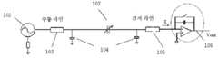
터치 포인트를 측위하기 위한 검출 장치가 터치 포인트를 검출하는 프로세스 동안, 터치 구동 라인들이 한 라인씩 스캐닝되며; 각각의 터치 구동 라인이 스캐닝될 때, 모든 터치 감지 라인들 상의 신호들이 판독되고; 터치 구동 라인들을 한 라인씩 스캐닝함으로써 터치 구동 라인들과 터치 감지 라인들의 모든 교차 포인트들이 스캐닝되어, 스캐닝 프로세스 동안 터치 포인트의 위치가 검출될 수 있다. 이 같은 터치 포인트를 측위하기 위한 검출 모드는 복수의 포인트의 좌표들을 명확히 결정할 수 있으며, 따라서 다중 터치가 실현될 수 있다. 검출 장치의 등가 회로 모델이 도 1에 도시되어 있으며, 이는 신호 소스(101), 터치 구동 라인(103)의 저항, 구동 라인과 감지 라인 사이의 상호 용량(102), 터치 구동 라인과 공통 전극 층 사이의 기생 용량(104), 터치 감지 라인과 공통 전극 층 사이의 기생 용량(104), 터치 감지 라인의 저항(105) 및 검출 회로(106)를 포함한다. 손가락이 터치 패널을 터치할 때, 전류의 일부가 손가락으로 흐르며, 이는 터치 구동 라인과 터치 감지 라인 사이의 상호 용량의 변화와 등가이고, 이로써 검출 단자에서 약한 전류 변화가 검출된다.During the process of the detection device for positioning the touch point detecting the touch point, the touch drive lines are scanned line by line; When each touch drive line is scanned, signals on all touch sense lines are read; By scanning the touch drive lines line by line, all intersection points of the touch drive lines and the touch sense lines can be scanned so that the position of the touch point can be detected during the scanning process. The detection mode for positioning such touch points can clearly determine the coordinates of the plurality of points, so that multiple touches can be realized. An equivalent circuit model of the detection device is shown in FIG. 1, which is the
본 발명의 실시예들에서 제공되는 인셀 터치 패널에서는, 터치 구동 라인들 및 터치 감지 라인들이 디스플레이 스크린 내에 배열되며, 각각의 터치 구동 라인은 하나 이상의 터치 스캐닝 박막 트랜지스터(TFT)를 통해 하나 이상의 게이트 라인에 접속되고, 하나의 터치 스캐닝 TFT는 하나의 게이트 라인에 대응하고, 하나의 터치 구동 라인은 복수의 터치 스캐닝 TFT에 대응할 수 있다. 따라서, 하나의 터치 구동 라인에 대응하는 게이트 라인들이 턴온될 때, 터치 구동 IC가 터치 구동 라인을 충전시키는데, 즉 터치 구동 신호를 입력한다. 터치 구동 신호가 인가되는 터치 구동 라인 및 일정한 전압이 인가되는 터치 감지 라인에 의해 터치 기능이 실현된다.In an in-cell touch panel provided in embodiments of the present invention, touch drive lines and touch sense lines are arranged in a display screen, each touch drive line having one or more gate lines through one or more touch scanning thin film transistors (TFTs). One touch scanning TFT may correspond to one gate line, and one touch driving line may correspond to the plurality of touch scanning TFTs. Therefore, when the gate lines corresponding to one touch driving line are turned on, the touch driving IC charges the touch driving line, that is, inputs a touch driving signal. The touch function is realized by a touch driving line to which a touch driving signal is applied and a touch sensing line to which a constant voltage is applied.
구체적으로, 게이트 라인들에 일대일로 대응하는 복수의 터치 스캐닝 TFT가 액정 디스플레이 패널 내의 어레이 기판의 주변 영역(비표시 영역)에 배열될 수 있으며, 각각의 터치 스캐닝 TFT는 터치 스캐닝 TFT에 대응하는 게이트 라인에 접속된 게이트, 터치 구동 회로에 접속된 소스, 및 터치 구동 라인에 접속된 드레인을 갖는다. 터치 스캐닝 TFT를 턴온시키거나 턴오프시킴으로써 터치 스캐닝 TFT에 접속된 터치 구동 라인에 터치 구동 신호가 인가되거나 그로부터 제거된다. 터치 스캐닝 TFT의 턴온 또는 턴오프는 화상을 디스플레이하기 위해 게이트 라인에 의한 TFT들의 턴온 또는 턴오프와 동기화된다.Specifically, a plurality of touch scanning TFTs corresponding one-to-one to the gate lines may be arranged in the peripheral area (non-display area) of the array substrate in the liquid crystal display panel, each touch scanning TFT having a gate corresponding to the touch scanning TFT. A gate connected to the line, a source connected to the touch drive circuit, and a drain connected to the touch drive line. By turning the touch scanning TFT on or off, the touch driving signal is applied to or removed from the touch drive line connected to the touch scanning TFT. The turn on or turn off of the touch scanning TFT is synchronized with the turn on or turn off of the TFTs by the gate line to display an image.
터치 구동 신호(터치 구동 클럭 신호)를 인가하기 위한 터치 구동 회로는 화상을 디스플레이하기 위한 디스플레이 구동 회로에 독립적이며, 터치 구동 클럭 신호의 주파수 및 크기는 실제 요구조건들에 따라 설정될 수 있다. 인셀 터치 패널은 간단한 구조, 더 얇은 두께, 기술적으로 간단한 제조 공정 및 저비용과 같은 장점들을 갖는다.The touch driving circuit for applying the touch driving signal (touch driving clock signal) is independent of the display driving circuit for displaying the image, and the frequency and magnitude of the touch driving clock signal can be set according to actual requirements. In-cell touch panels have advantages such as simple structure, thinner thickness, technically simple manufacturing process and low cost.
이하에서 본 발명의 실시예들에서 제공되는 기술적 해법을 총괄적으로 소개한다.Hereinafter, the technical solutions provided in the embodiments of the present invention will be introduced as a whole.
본 발명의 실시예에서 제공되는 인셀 터치 패널은 서로 대향하게 배열된 제1 기판과 제2 기판을 포함하고, 제1 기판 상에는 수평 배열된 복수의 게이트 라인이 형성되며; 인셀 터치 패널은, 수평 배열된 복수의 터치 구동 라인; 수직 배열된 복수의 터치 감지 라인; 및 복수의 터치 스캐닝 TFT를 더 포함하고, 각각의 터치 스캐닝 TFT는 하나의 게이트 라인에 접속된 게이트, 터치 구동 회로에 접속된 소스, 및 하나의 터치 구동 라인에 접속된 드레인을 가지며, 게이트 라인은 하나의 터치 스캐닝 TFT의 게이트에만 접속되는데; 여기에서, 게이트 라인들의 개수 ≥ 터치 스캐닝 TFT들의 개수 ≥ 터치 구동 라인들의 개수이다.The in-cell touch panel provided in the embodiment of the present invention includes a first substrate and a second substrate arranged opposite to each other, and a plurality of horizontally arranged gate lines are formed on the first substrate; The in-cell touch panel includes a plurality of touch drive lines arranged horizontally; A plurality of touch sensing lines arranged vertically; And a plurality of touch scanning TFTs, each touch scanning TFT having a gate connected to one gate line, a source connected to a touch driving circuit, and a drain connected to one touch driving line, the gate line having Connected only to the gate of one touch scanning TFT; Here, the number of gate lines ≥ the number of touch scanning TFTs ≥ the number of touch driving lines.
일례에서, 각각의 터치 구동 라인은 하나 이상의 터치 스캐닝 TFT의 드레인을 통해 하나 이상의 터치 스캐닝 TFT에 접속된다.In one example, each touch drive line is connected to one or more touch scanning TFTs through the drain of one or more touch scanning TFTs.
일례에서, 하나의 터치 구동 라인에 접속된 복수의 터치 스캐닝 TFT에 대응하는 게이트 라인들은 서로 인접한다.In one example, the gate lines corresponding to the plurality of touch scanning TFTs connected to one touch drive line are adjacent to each other.
일례에서, 인셀 터치 패널은 제1 기판 상에 수직 배열된 복수의 데이터 라인을 더 포함하고; 복수의 터치 구동 라인은 제1 기판 상에 배치되고, 데이터 라인들과 동일한 층 상에 배열되며; 복수의 터치 구동 라인의 각각은 인접하는 2개의 데이터 라인 사이에 복수의 구동 세그먼트를 포함하고; 동일한 데이터 라인의 양측에 배치된 구동 세그먼트들은 스루-홀 바이패스(through hole bypass)에 의해 서로 접속되며, 복수의 터치 감지 라인은 제2 기판 상에 배치된다.In one example, the in-cell touch panel further includes a plurality of data lines arranged vertically on the first substrate; A plurality of touch drive lines are disposed on the first substrate and arranged on the same layer as the data lines; Each of the plurality of touch drive lines includes a plurality of drive segments between two adjacent data lines; Drive segments disposed on both sides of the same data line are connected to each other by through hole bypass, and the plurality of touch sense lines are disposed on the second substrate.
일례에서, 터치 스캐닝 TFT들은 제1 기판의 비표시 영역, 즉 주변 영역에 배열된다.In one example, the touch scanning TFTs are arranged in the non-display area, that is, the peripheral area of the first substrate.
일례에서, 인셀 터치 패널은 수직 배열된 복수의 터치 구동 전극 유닛을 더 포함하고, 복수의 터치 구동 전극 유닛의 각각은 하나 이상의 터치 구동 전극을 포함하고, 터치 구동 전극 유닛들의 각각은 하나의 터치 구동 라인에 전기적으로 접속되며, 터치 구동 전극 유닛은 픽셀 유닛들의 인접하는 2개의 열 사이에 배열된다.In one example, the in-cell touch panel further comprises a plurality of touch drive electrode units arranged vertically, each of the plurality of touch drive electrode units comprising one or more touch drive electrodes, each of the touch drive electrode units being one touch drive. Electrically connected to the line, the touch drive electrode unit is arranged between two adjacent rows of pixel units.
일례에서, 인접하는 터치 감지 라인들 사이의 갭은 제1 기판 상의 터치 구동 전극 유닛에 대향하고, 터치 감지 라인들의 각각은 픽셀 유닛들의 하나 이상의 열에 대향한다.In one example, the gap between adjacent touch sense lines faces the touch drive electrode unit on the first substrate, and each of the touch sense lines faces one or more columns of pixel units.
일례에서, 복수의 터치 구동 전극 유닛의 각각에서, 복수의 인접하는 터치 구동 전극이 게이트 라인 또는 데이터 라인과 동일한 폭을 갖는 금속 와이어(wire)를 통해 서로 전기적으로 접속된다.In one example, in each of the plurality of touch drive electrode units, the plurality of adjacent touch drive electrodes are electrically connected to each other through a metal wire having the same width as the gate line or the data line.
일례에서, 각 터치 구동 전극 유닛의 길이는 10㎛~150㎛일 수 있다.In one example, the length of each touch driving electrode unit may be 10 μm to 150 μm.
일례에서, 각 터치 구동 전극 유닛의 폭은 어레이 기판 상의 서브픽셀 유닛의 폭과 동일하다.In one example, the width of each touch drive electrode unit is equal to the width of the subpixel units on the array substrate.
일례에서, 각 터치 구동 전극은 수직적으로 서로 인접하는 2개의 서브픽셀 유닛에 대응하는 게이트 라인들 사이에 배치된다.In one example, each touch drive electrode is disposed between gate lines corresponding to two subpixel units that are vertically adjacent to each other.
일례에서, 각 터치 스캐닝 TFT의 소스에 접속된 터치 구동 회로 및 화상을 디스플레이하도록 게이트 라인들을 구동하기 위한 구동 회로는 집적된 칩 IC 내에 배열된다.In one example, the touch driving circuit connected to the source of each touch scanning TFT and the driving circuit for driving the gate lines to display the image are arranged in the integrated chip IC.
이어서, 본 발명의 실시예들에서 제공되는 기술적 해법들을 첨부 도면들을 참조하여 상세히 설명한다.Next, the technical solutions provided in the embodiments of the present invention will be described in detail with reference to the accompanying drawings.
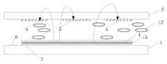
도 2를 참조하면, 본 발명의 실시예에서 제공되는 인셀 터치 패널은 서로 대향하게 배열된 제1 기판(1)과 제2 기판(2)을 포함하고, 제1 기판(1) 상에는 수평 배열된 복수의 게이트 라인(3)이 형성된다. 인셀 터치 패널은 수평 배열된 복수의 터치 구동 라인(4), 수직 배열된 복수의 터치 감지 라인(5), 및 복수의 터치 스캐닝 TFT(6)를 더 포함하는데, 각 터치 스캐닝 TFT(6)는 하나의 게이트 라인(3)에 접속된 게이트, 터치 구동 회로(도 2에 도시되지 않음)에 접속된 소스, 및 하나의 터치 구동 라인(4)에 접속된 드레인을 갖고, 게이트 라인(3)은 하나의 터치 스캐닝 TFT(6)의 게이트에만 접속되며, 여기에서 게이트 라인들의 개수 ≥ 터치 스캐닝 TFT들의 개수 ≥ 터치 구동 라인들의 개수이다.Referring to FIG. 2, an in-cell touch panel provided in an embodiment of the present invention includes a
예를 들어, m개의 게이트 라인, n개의 터치 스캐닝 TFT(6) 및 l개의 터치 구동 라인이 배열될 수 있으며, m, n 및 l은 양의 정수들이다. 다음과 같은 여러 예가 존재한다.For example, m gate lines, n
m=n 및 n=l일 때, 각 게이트 라인이 하나의 터치 스캐닝 TFT에 접속되고, 각 터치 구동 라인이 하나의 스캐닝 TFT에 접속되는데, 즉 게이트 라인, 터치 스캐닝 TFT 및 터치 구동 라인이 서로 일대일로 대응한다.When m = n and n = l, each gate line is connected to one touch scanning TFT, and each touch driving line is connected to one scanning TFT, that is, the gate line, touch scanning TFT and touch driving line are one-to-one with each other. Corresponds to
m=n 및 n>l일 때, 각 게이트 라인은 하나의 터치 스캐닝 TFT에 접속되고, 각 터치 구동 라인은 복수의 터치 스캐닝 TFT에 접속되는데, 즉 하나의 터치 구동 라인이 복수의 터치 스캐닝 TFT에 대응하고, 복수의 터치 스캐닝 TFT의 각각은 하나의 게이트 라인에 각각 대응한다.When m = n and n> l, each gate line is connected to one touch scanning TFT, and each touch driving line is connected to a plurality of touch scanning TFTs, that is, one touch driving line is connected to the plurality of touch scanning TFTs. And each of the plurality of touch scanning TFTs respectively corresponds to one gate line.
m>n 및 n>l일 때, 하나의 터치 스캐닝 TFT는 하나의 게이트 라인에 접속되고, 각각의 터치 구동 라인은 복수의 터치 스캐닝 TFT에 접속되는데, 즉 일부 게이트 라인들은 터치 스캐닝 TFT에 접속되지 않는다.When m> n and n> l, one touch scanning TFT is connected to one gate line, and each touch driving line is connected to a plurality of touch scanning TFTs, that is, some gate lines are not connected to the touch scanning TFT. Do not.
터치 스캐닝 TFT들에 접속되지 않은 게이트 라인들은 화상을 디스플레이하는 데에만 사용되며, 터치 스캐닝 TFT들에 접속된 게이트 라인들은 화상의 디스플레이 및 터치 기능의 둘 다를 실현하는 데 사용된다.Gate lines not connected to the touch scanning TFTs are used only to display an image, and gate lines connected to the touch scanning TFTs are used to realize both display and touch function of the image.
여기서, 터치 스캐닝 TFT(6)의 게이트는 게이트 라인(3)에 직접 접속된 독립적 구조로서 설정될 수 있고, 터치 스캐닝 TFT(6)는 또한 게이트 라인(3)의 상부에 직접 제조될 수 있으며, 게이트 라인(3)은 터치 스캐닝 TFT(6)의 게이트로서 직접 이용될 수도 있다.Here, the gate of the
도 2에 도시된 바와 같이, 액정 디스플레이(LCD)에 내장된 터치 패널을 일례로써 가져오면, 제1 기판(1)과 제2 기판(2) 사이에 액정(12)이 채워지고, 게이트 라인(3)과 터치 구동 라인(4)은 격리 층(15)을 통해 격리된다.As shown in FIG. 2, when a touch panel embedded in a liquid crystal display (LCD) is taken as an example, the
도 3은 도 2에 도시된 인셀 터치 패널의 평면도이다.FIG. 3 is a plan view of the in-cell touch panel shown in FIG. 2.
도 3에 도시된 제1 기판(1) 상에는, 수평 배열된 복수의 게이트 라인(3), 게이트 라인들(3)과 평행하게 배열된 복수의 터치 구동 라인(4), 복수의 게이트 라인(3)에 각각 접속된 복수의 TFT(6), 모든 TFT들(6)에 접속된 터치 구동 IC, 및 복수의 터치 구동 라인(4)에 대해 수직으로 배열된 제1 기판(1) 또는 제2 기판(2) 상의 복수의 터치 감지 라인(5)이 포함된다. 실제 제조된 터치 패널에서, 복수의 터치 감지 라인(5)은 소정의 폭을 갖는 도전성 막대일 수 있다.On the
터치 스캐닝 TFT(6)는 제1 기판(1)의 주변 영역에 배치되며(주변 영역은 디스플레이 패널 상의 비표시 영역을 지칭함), TFT(6)는 게이트 라인에 접속되므로, TFT(6)는 통상적으로 게이트 라인의 인출 위치에 가까운 제1 기판(1) 상에 배열된다.The
이하에서 터치 기능을 달성하기 위한 도 2 및 3에 도시된 인셀 터치 패널의 원리를 간단히 소개한다.Hereinafter, the principle of the in-cell touch panel illustrated in FIGS. 2 and 3 for achieving a touch function will be briefly introduced.
구체적 구현에서, 터치 감지 라인(5)에 일정한 전압이 인가되고, 터치 구동 라인(4)에 접속된 터치 구동 회로를 통해 터치 구동 라인(4)에 터치 구동 신호가 인가되며, 터치 구동 신호는 고주파 신호이다. 터치 구동 라인(4)과 터치 감지 라인(5) 사이에 전기장이 형성되고, 전기장은 투사 전기장으로서 지칭되며, 터치 포인트가 측위되는 영역의 투사 전기장의 변화를 검출함으로써 터치 포인트가 측위된다.In a specific embodiment, a constant voltage is applied to the
터치 구동 회로는 터치 구동 IC 내에 배열된다.The touch drive circuit is arranged in the touch drive IC.
도 4에 도시된 바와 같이, 터치 구동 라인(4)과 터치 감지 라인(5) 사이에 전기장이 형성되고, 화살표를 가진 곡선은 전기장 라인의 방향을 가리킨다. 도 4로부터, 인접하는 터치 감지 라인들(5) 사이에 갭이 존재하고, 따라서 터치 구동 라인(4)과 터치 감지 라인(5) 사이의 전기장이 터치 감지 전극 층을 통과하여 제2 기판(2)의 외측에 도달할 수 있으며, 따라서 제2 전극(2)의 외측에 발생하는 터치 행위를 더 잘 감지할 수 있다는 것을 알 수 있다.As shown in FIG. 4, an electric field is formed between the
터치 패널이 동작할 때, 터치 감지 라인들(5) 각각 상에는 일정한 전압이 항상 존재하며, 각각의 터치 구동 라인(4) 상의 터치 구동 신호는 펄스 신호로서 입력된다. 터치 구동 라인(4)에 접속된 터치 스캐닝 TFT(6)가 턴온될 때, 터치 구동 회로에 의해 터치 구동 라인(4)에 터치 구동 신호가 인가된다. 터치 스캐닝 TFT(6)의 턴온 및 턴오프는 터치 스캐닝 TFT(6)에 접속된 게이트 라인에 의해 제어되며, 화상의 디스플레이를 제어하기 위한 칩 IC가 게이트 라인(3)을 스캐닝할 때, 즉 게이트 라인(3)에 디스플레이 구동 전압을 인가할 때, 게이트 라인(3)에 접속된 (터치 스캐닝 TFT(6)를 포함하는) 모든 TFT들이 턴온된다.When the touch panel is operating, a constant voltage is always present on each of the
화상을 디스플레이할 때, 각 게이트 라인들을 스캐닝하는 속도가 매우 빠르며, 따라서 게이트 라인은 단위 시간 내에 매우 빈번하게 턴온되고, 따라서 터치 스캐닝 TFT(6)가 매우 빈번하게 턴온되며, 따라서 터치 기능을 달성하기 위한 터치패널의 요구조건들을 충족할 수 있다.When displaying an image, the speed of scanning the respective gate lines is very fast, so the gate lines are turned on very frequently in unit time, and thus the
도 5는 본 발명의 실시예들에 따른, 화상의 디스플레이 및 터치 기능을 달성할 때의 신호들의 타이밍 순서도이다.5 is a timing flowchart of signals when achieving a display and touch function of an image, in accordance with embodiments of the present invention.
터치 디스플레이 기능을 달성하기 위한 본 발명에서 제공되는 터치 패널의 원리를 도 2 내지 5를 참조하여 상세히 설명한다.The principle of the touch panel provided in the present invention for achieving the touch display function will be described in detail with reference to FIGS. 2 to 5.
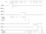
화상을 디스플레이하기 위해 게이트 라인이 스캐닝될 때, 일 회의 스캐닝 사이클(또는 하나의 스캐닝 펄스) 내에서, 하나 이상의 CLK 펄스 신호가 도 4의 터치 구동 IC에 의해 게이트 라인에 접속된 터치 구동 라인(4)에 입력될 수 있다.When the gate line is scanned to display an image, within one scanning cycle (or one scanning pulse), one or more CLK pulse signals are connected to the gate line by the touch driver IC of FIG. 4. ) Can be entered.
도 5에 도시된 바와 같이, CLK 신호는 터치 구동 IC에 의해 제공되는 터치 구동 신호이다. 도 5는 터치 구동 IC가 소정의 시간 간격으로 터치 구동 라인(4)에 2개의 CLK 신호 펄스를 입력하는 것을 보여준다. 더욱이, 도 5에 도시된 바와 같이, 게이트 라인 n, 게이트 라인 n+1, 게이트 라인 n+2 및 게이트 라인 n+3은 협동하여 제1 터치 구동 라인에 입력되는 터치 구동 신호를 제어하고, 게이트 라인 m, 게이트 라인 m+1, 게이트 라인 m+2 및 게이트 라인 m+3은 협동하여 제2 터치 구동 라인에 입력되는 터치 구동 신호를 제어한다.As shown in Fig. 5, the CLK signal is a touch drive signal provided by the touch drive IC. 5 shows that the touch drive IC inputs two CLK signal pulses to the
통상 게이트 라인을 스캐닝하기 위한 스캐닝 사이클 내에서, 소정의 시간 간격으로 2개의 CLK 신호 펄스를 터치 구동 라인(4)에 입력하여 더 양호한 터치 검출 효과를 달성할 수 있고, 하나의 스캐닝 사이클 내에서 더 많은 CLK 신호 펄스가 입력될수록 터치 구동 라인의 스캐닝 주파수는 더 높으며, 따라서 터치 검출 효과는 더 양호한 반면, 이에 따라 터치 구동 IC에 대한 요구조건들이 증가하고, 따라서 전체 인셀 터치 패널의 제조 비용이 증가한다는 점에 유의해야 한다.Within the scanning cycle for scanning the gate line normally, two CLK signal pulses can be input to the
터치 스캐닝 TFT(6)의 턴온은 화상을 디스플레이하기 위해 터치 스캐닝 TFT(6)에 접속된 게이트 라인 상의 다른 TFT들의 통상의 동작들에 영향을 미치지 않는다.The turn on of the
본 발명의 실시예들에서, 이것은 종래 기술에서 게이트 라인에 접속된 터치 스캐닝 TFT(6)를 턴온하기 위해 게이트 라인이 스캐닝될 때, 게이트 라인에 인가되는 턴온 전압을 이용하는 반면, 터치 구동 신호는 터치 스캐닝 TFT(6)에 접속된 터치 구동 라인에 입력되며, 따라서 터치 구동 신호가 인가되는 터치 구동 라인 및 일정한 전압이 인가되는 터치 감지 라인에 의해 터치 기능이 달성된다.In embodiments of the present invention, this uses the turn-on voltage applied to the gate line when the gate line is scanned to turn on the
터치 구동 라인(4)은 제1 기판(1) 상에 배열되며, 터치 감지 라인(5)은 제1 기판(1) 또는 제2 기판(2) 상에 배열될 수 있다.The
본 발명의 실시예들은 액정 디스플레이의 분야뿐만 아니라 전기 발광 유기 발광 다이오드(OLED)의 분야와 같은 다른 디스플레이들의 분야에도 적용될 수 있다.Embodiments of the present invention can be applied to the field of liquid crystal displays as well as other displays, such as the field of electroluminescent organic light emitting diodes (OLEDs).
본 발명의 실시예들이 액정 디스플레이의 분야에 적용될 때, 터치 구동 라인들(4)은 (제1 기판(1)에 대응하는) 어레이 기판 상에 배열되고, 터치 감지 라인들은 (제2 기판(2)에 대응하는) 컬러 필름 기판 상에 배열될 수 있다. 구체적으로, 도 6에 도시된 바와 같이, 터치 감지 라인들은 제2 기판(2)의 액정과 접촉하는 일측 상에 배열될 수 있는데, 특히 터치 감지 라인들은 투명 전극들과 함께 동일 층 상에, 즉 RGB 수지 층(8)의 상부에 배열될 수 있다. 일례에서, 제2 기판(2) 상의 투명 전극은 (TN 타입의 LCD의 경우에) ITO 공통 전극 또는 (IPS 타입 또는 FFS 타입의 LCD의 경우에) 정전기 차폐를 위한 ITO 차폐 전극일 수 있다. 대안으로서, 도 7에 도시된 바와 같이, 터치 감지 라인들은 RGB 수지 층(8)과 제2 기판(2) 사이에 배열될 수도 있다.When embodiments of the present invention are applied in the field of liquid crystal displays,
본 발명의 실시예들이 OLED 디스플레이의 분야에 적용될 때, 터치 구동 라인들(4) 및 터치 감지 라인들(5)은 인셀 터치 패널의 제1 기판 또는 제2 기판 상의 상이한 층들 상에 배열될 수 있다.When embodiments of the invention are applied in the field of OLED displays,
터치 패널을 위한 게이트 라인들의 개수는 터치 정밀도에 대한 요구치 및 터치 패널의 크기에 따라 설정될 수 있다. 터치 정밀도에 대한 요구치가 비교적 더 높고 및/또는 터치 패널의 크기가 더 클 때, 어레이 기판 상에 터치 기능을 달성하기 위한 게이트 라인이 더 많이 배열될 수 있고, 터치 정밀도에 대한 요구치가 비교적 더 낮고 및/또는 터치 패널의 크기가 더 작을 때, 어레이 기판 상에 터치 기능을 달성하기 위한 게이트 라인이 더 적게 배열될 수 있다. 제1 기판(1) 상의 모든 게이트 라인들 또는 게이트 라인들의 일부를 제어함으로써 터치 구동 라인들에 터치 구동 신호들이 인가된다. 터치 스캐닝 TFT(6)에 접속된 모든 게이트 라인들은 터치 스캐닝 TFT(6)를 턴온 또는 턴오프되도록 제어할 수 있으며, 터치 구동 신호들이 터치 구동 라인들에 인가되는 동안의 시간, 즉 각 터치 구동 라인의 스캐닝 시간을 더 제어할 수 있다.The number of gate lines for the touch panel may be set according to the requirement for touch precision and the size of the touch panel. When the demand for touch precision is relatively higher and / or the size of the touch panel is larger, more gate lines can be arranged on the array substrate to achieve touch functionality, and the demand for touch precision is relatively lower and And / or when the touch panel is smaller in size, fewer gate lines may be arranged on the array substrate to achieve touch functionality. Touch drive signals are applied to the touch drive lines by controlling all the gate lines or some of the gate lines on the
일례에서, 도 8에 도시된 바와 같이, 본 발명의 일 실시예에서 제공되는 바와 같은 인셀 터치 패널은, 제1 기판(1) 상에 수직 배열된 복수의 데이터 라인(14), 제1 기판(1) 상에 수평 배열된 복수의 터치 구동 라인(4) - 터치 구동 라인들(4)은 도 6에 도시된 바와 같이 제1 기판(1) 상의 데이터 라인들(14)과 동일한 층 상에 배열될 수 있으며, 또한 별개의 층 상에 배열될 수 있음 - , 제2 기판(2) 상의 투명 전극들과 동일한 층 상에 배열된 복수의 터치 감지 라인(5)을 더 포함한다.In one example, as shown in FIG. 8, an in-cell touch panel as provided in an embodiment of the present invention includes a plurality of
여기서, 터치 구동 라인들(4)은 제1 기판(1) 상의 데이터 라인들(14)과 동일한 층 상에 배열될 수 있으며, 따라서 터치 구동 라인들(4) 및 데이터 라인들(14)은 동일 프로세스에서 제조될 수 있고, 이는 공정 흐름을 줄이고 공정 절차를 간소화한다. 한편, 데이터 라인들(14)과 터치 구동 라인들(4) 사이에 단락이 형성되거나 신호들 사이에 크로스토크(crosstalk)가 발생하는 문제를 방지하기 위해, 제조 프로세스에서 데이터 라인들(14) 및 터치 구동 라인들(4)을 서로 격리시켜야 한다.Here, the
터치 구동 라인들(4)은 개별 층으로서 배열될 수 있고, 격리 층을 통해 데이터 라인들(14)로부터 격리되며, 이는 터치 구동 라인들(4)과 데이터 라인들(14) 사이에 형성되는 단락 또는 크로스토크의 문제를 완전히 방지할 수 있으며, 데이터 라인들(14)이 배치되는 필름 층의 상부에 터치 구동 라인들(14)이 배치되는 필름 층이 배열될 수 있다.The
터치 구동 라인들(4)이 제1 기판(1) 상의 데이터 라인들(14)과 동일한 층 상에 배열될 때, 데이터 라인들에서 형성되는 크로스토크의 문제를 방지하기 위해, 도 8에 도시된 바와 같은 일례에서, 각 터치 구동 라인(4)은 복수의 터치 구동 라인 세그먼트(segment)를 포함하는데, 이들 각각은 인접하는 2개의 데이터 라인(14) 사이에 위치하고, 동일한 데이터 라인(14)의 양측에 위치하는 터치 구동 세그먼트들은 스루-홀 바이패스에 의해 접속될 수 있다.When the
구체적으로, 다음과 같이 스루-홀 바이패스에 의해 접속이 이루어질 수 있다. 동일한 데이터 라인(14)의 양측의 터치 구동 세그먼트들은 게이트 금속 층 상에 위치하거나 인듐 주석 산화물(ITO)의 픽셀 전극 층 상에 위치하는 접속 전극들을 통해 접속될 수 있고, 접속 전극들은 각각 스루-홀에 의해 동일한 데이터 라인의 양측의 터치 구동 라인 세그먼트들에 접속된다.Specifically, the connection may be made by through-hole bypass as follows. The touch drive segments on both sides of the
하나의 게이트 라인 상의 터치 스캐닝 TFT가 터치 구동 라인에 입력될 터치 구동 신호를 제어할 수 있거나, 복수의 게이트 라인 상의 터치 스캐닝 TFT들이 동일 터치 구동 라인에 입력될 터치 구동 신호를 제어할 수 있다. 즉, 각 터치 구동 라인이 하나의 터치 스캐닝 TFT의 드레인에 접속되거나, 각 터치 구동 라인이 복수의 터치 스캐닝 TFT들의 드레인에 접속된다.The touch scanning TFT on one gate line may control the touch driving signal to be input to the touch driving line, or the touch scanning TFTs on the plurality of gate lines may control the touch driving signal to be input to the same touch driving line. That is, each touch drive line is connected to the drain of one touch scanning TFT, or each touch drive line is connected to the drain of the plurality of touch scanning TFTs.
도 3에 도시된 바와 같이, 인셀 터치 패널의 하나의 터치 구동 라인(4)이 4개의 터치 스캐닝 TFT(6)에 접속되고, 터치 구동 라인(4)에 접속된 터치 스캐닝 TFT들(6)이 순차적으로 턴온될 때, 터치 구동 라인(4)에 접속된 터치 스캐닝 TFT들(6)은 동일한 터치 구동 라인(4)에 순차적으로 터치 구동 신호를 입력한다.As shown in FIG. 3, one
복수의 게이트 라인 상의 터치 스캐닝 TFT들에 의해 동일 터치 구동 라인에 대한 터치 구동 신호의 입력을 제어하는 것은 단위 시간에서의 터치 구동 라인에 충전 횟수, 즉 터치 구동 신호의 입력 횟수를 증가시킬 수 있으며, 단위 시간에 터치 구동 라인을 충전하는 횟수가 많을수록 터치 감지의 효과는 더 양호하며, 따라서 터치 정밀도가 더 높다.Controlling the input of the touch drive signal for the same touch drive line by the touch scanning TFTs on the plurality of gate lines may increase the number of charges of the touch drive line, that is, the number of inputs of the touch drive signal in unit time, The more the number of times the touch drive line is charged in unit time, the better the effect of touch sensing, and therefore the higher the touch precision.
도 2에 도시된 바와 같이, 터치 구동 라인은 폭이 좁다. 통상의 터치 기능을 실현하기 위하여, 본 발명의 일 실시예에서는 터치 기능을 실현하기 위한 터치 구동 라인이 구조적으로 최적화된다.As shown in FIG. 2, the touch drive line is narrow. In order to realize the normal touch function, in one embodiment of the present invention, the touch drive line for realizing the touch function is structurally optimized.
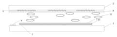
특히, 도 9를 참조하면, 본 발명에서 제공되는 인셀 터치 패널은 수직 방향으로 배열된 복수의 터치 구동 전극 유닛(41)을 더 포함하며, 각 터치 구동 전극 유닛(41)은 하나 이상의 터치 구동 전극(411)을 포함하고, 각 터치 구동 전극 유닛(41)은 하나의 터치 구동 라인(4)에 전기적으로 접속되며, 각 터치 구동 전극 유닛(41)은 픽셀 유닛들의 인접하는 2개의 열 사이에 배열되는데, 즉 터치 구동 전극 유닛(41)은 공간적으로 제2 기판 상의 인접하는 2개의 터치 감지 라인(5) 사이의 갭(gap)에 대향한다.In particular, referring to FIG. 9, the in-cell touch panel provided in the present invention further includes a plurality of touch driving
일례에서, 도 10에 도시된 바와 같이, 인접하는 2개의 터치 감지 라인(5) 사이의 갭은 제1 기판(1) 상의 터치 구동 전극 유닛(41)에 대향하는데, 즉 인접하는 2개의 터치 감지 라인(5) 사이의 갭은 제1 기판(1) 상의 픽셀 유닛들(13)의 인접하는 2개의 열 사이의 갭에 대향하고, 하나의 터치 감지 라인(5)은 (도 10에 도시된 바와 같이) 픽셀 유닛들(13)의 하나의 열에 대향하거나, 픽셀 유닛들의 복수의 열에 대향하며(도 10에 도시되지 않음), 각 픽셀 유닛은 적어도 3개의 서브픽셀 RGB를 포함한다.In one example, as shown in FIG. 10, the gap between two adjacent
일례에서, 복수의 이웃하는 터치 구동 전극 유닛(41)이 터치 구동 라인(4)을 통해 서로 전기적으로 접속된다.In one example, the plurality of neighboring touch
일례에서, 각 터치 구동 전극 유닛(41)의 길이는 10㎛~150㎛이고, 이것은 요구되는 터치 패널의 크기 및 개구율에 의존한다. 터치 패널이 더 큰 크기를 갖는 경우, 각 터치 구동 전극 유닛(41)의 길이를 더 길게 설정될 수 있으며, 그렇지 않은 경우에는 더 짧게 설정될 수 있다.In one example, the length of each touch
일례에서, 각 터치 구동 전극 유닛(41)의 폭은 어레이 기판 상의 하나의 서브픽셀 유닛의 폭과 동일하지만, 하나의 서브픽셀 유닛의 폭으로 한정되는 것이 아니며, 실제 요구 조건들에 따라 설정될 수 있다. 개구율에 대한 요구치가 더 낮은 경우, 터치 구동 전극 유닛(41)의 폭을 더 넓게 설정될 수 있으며, 이와 달리 개궁율에 대한 요구치가 더 큰 경우, 폭을 더 좁게 설정될 수 있다.In one example, the width of each touch
일례에서, 각 터치 구동 전극(411)은 인접하는 2개의 서브픽셀 유닛에 대응하는 게이트 라인들 사이에 수직 방향으로 배치된다(도 9에 도시되지 않음). 각 터치 구동 전극(411)의 길이는 하나의 서브픽셀 유닛의 길이와 동일하거나, 하나의 서브픽셀 유닛의 길이보다 짧을 수 있다.In one example, each
바람직하게는, 각 터치 구동 전극 유닛(41)을 구성하는 인접하는 터치 구동 전극들(411) 사이의 접속 부분의 폭은 터치 구동 전극(411) 자체의 폭보다 좁고; 바람직하게는 수직 방향으로 인접하는 터치 구동 전극들(411)은 데이터 라인 또는 게이트 라인의 폭과 동일하거나 근접한 폭을 갖는 금속 와이어에 의해 접속될 수 있음으로써, 게이트 라인과 오버랩되는 터치 구동 전극 유닛(41)의 영역을 줄일 수 있고, 통상의 화상을 디스플레이하기 위한 게이트 라인에 영향을 주지 않고 게이트 라인과의 상호 용량을 줄일 수 있다.Preferably, the width of the connection portion between adjacent
일례에서, 제1 기판의 상이한 영역들에 위치한 터치 구동 전극들은 크기가 동일하며, 터치 구동 전극 유닛들이 동일하다. 즉, 각 터치 구동 전극 유닛은 동일 폭 및 동일 길이를 가지며, 각 터치 구동 전극 유닛은 동일한 수의 터치 구동 전극을 포함한다.In one example, touch drive electrodes located in different regions of the first substrate are the same size, and touch drive electrode units are the same. That is, each touch driving electrode unit has the same width and the same length, and each touch driving electrode unit includes the same number of touch driving electrodes.
일례에서, 동일 터치 구동 라인(4)에 접속된 터치 구동 전극 유닛(41)은 (도 9에 도시된 바와 같이) 동일 행에 속하는 인접하는 2개의 픽셀 유닛마다 사이에 배열될 수 있거나, 동일 행에 속하는 인접하는 픽셀 유닛들의 일부 사이에 배열될 수 있다.In one example, the touch
터치 감지의 효과에서 더 높은 정밀도를 달성하기 위하여, 바람직하게는 터치 구동 전극 유닛(41)은 동일 행에 속하는 인접하는 2개의 픽셀 유닛마다 사이에 배열된다. 일례에서, 제조 공정의 어려움을 줄이고, 통상의 터치 정밀도에 대한 요구치를 충족시키기 위하여, 터치 구동 전극 유닛(41)은 실제 요구 조건들에 따라 동일 행에 속하는 인접하는 픽셀 유닛들의 일부 사이에 배열되며, 인접하는 2개의 터치 구동 전극 유닛(41) 사이의 거리(L)는 실제 요구 조건들 및 실제 인셀 터치 패널의 크기에 따라 설계될 수 있다.In order to achieve higher precision in the effect of touch sensing, the touch
도 9에 도시된 바와 같이, 수직 방향으로 서로 인접하는 터치 구동 전극 유닛들(41) 사이의 거리는 하나의 픽셀 유닛의 길이와 동일하거나, 둘 이상의 픽셀 유닛의 길이들의 합일 수 있다.As shown in FIG. 9, the distance between the touch driving
일례에서, 수직 방향으로 서로 인접하는 2개의 터치 구동 전극 유닛(41) 사이의 거리는 요구 조건들에 따라 배열될 수 있는데, 즉 수직 방향으로 하나 이상의 픽셀 유닛의 길이들의 합이거나, 동일 열에서 인접하는 픽셀 유닛들 사이의 거리와 동일할 수 있다.In one example, the distance between two touch
도 11은 터치 구동 라인(4) 상에 배열된 복수의 터치 구동 전극 유닛(41)을 갖는 인셀 터치 패널의 개략적인 평면도의 일부이다. 전체적으로 볼 때, 구조적으로 최적화된 터치 구동 라인들은 수평 방향으로 배열된 소정의 폭을 갖는 도전성 막대들이며, 이는 터치 구동 라인들에 대한 터치 가능 영역을 증가시키고, 터치 패널의 감도를 향상시킨다.11 is a part of a schematic plan view of an in-cell touch panel having a plurality of touch
이하에서 본 발명의 일 실시예에서 제공되는 바와 같이 터치 감지 라인들(5)이 배열되는 모드를 설명한다.Hereinafter, a mode in which the
본 발명에서 제공되는 터치 감지 라인들은 투명한 도전성 막대들이며, 특히 인듐 주석 산화물(ITO)으로 제조될 수 있다.The touch sense lines provided in the present invention are transparent conductive rods, in particular can be made of indium tin oxide (ITO).
도 12에 도시된 바와 같이, 터치 감지 라인들(5)은 소정의 폭을 갖고 동일한 간격으로 배열된 복수의 도전성 막대이다.As shown in FIG. 12, the
각 터치 감지 라인(5)이 위치한 영역은 어레이 기판 상에 동일 열에 속하는 픽셀 유닛들이 배치되는 영역에 대응하는데, 즉 어레이 기판 상의 각 터치 감지 라인(5)의 투영 영역은 터치 감지 라인 아래에 동일 열에 속하는 픽셀 유닛들에 의해 덮힌 영역과 오버랩된다.The area where each
일례에서, 도 13을 참조하면, 이웃하는 터치 감지 라인들(5)의 일부는 와이어(9)를 통해 접속되어 터치 감지 라인들의 신호 수신을 향상시키는데, 예를 들어 2개 또는 3개의 이웃하는 도전성 막대가 와이어(9)를 통해 서로 접속된다. 따라서, 와이어(9)를 통해 접속된 복수의 독립적인 터치 감지 라인(5)이 더 넓은 터치 감지 라인을 구성한다.In one example, referring to FIG. 13, some of the neighboring
도 12 및 도 13에 도시된 바와 같이, 터치 감지 라인의 폭은 하나의 픽셀 유닛의 폭과 동일할 수 있으며, 복수의 픽셀 유닛의 폭들의 합과 동일할 수도 있는데, 즉 터치 감지 라인(5)은 픽셀 유닛들의 하나의 열만을 또는 순차적으로 서로 인접하는 픽셀 유닛들의 복수의 열을 덮는다. 터치 감지 라인(5)이 순차적으로 서로 인접하는 픽셀 유닛들의 복수의 열을 덮는 경우, 터치 감지 라인의 신호 수신이 향상된다.12 and 13, the width of the touch sensing line may be equal to the width of one pixel unit and may be equal to the sum of the widths of the plurality of pixel units, that is, the
일례에서, 각 터치 스캐닝 TFT(6)의 소스에 접속된 터치 구동 회로 및 화상을 디스플레이하도록 게이트 라인을 구동하기 위한 구동 회로는 집적된 칩 IC 내에 배열될 수 있다. 터치 구동 라인에 제공되는 CLK 신호는 화상을 디스플레이하기 위한 구동 신호에 독립적이다.In one example, the touch driving circuit connected to the source of each
요컨대, 본 발명의 실시예들에서, 인셀 터치 패널은 수평 배열된 복수의 게이트 라인, 수평 배열된 복수의 터치 구동 라인, 및 수직 배열된 복수의 터치 감지 라인을 포함하고, 인셀 터치 패널은 게이트 라인들에 일대일로 각각 대응하는 복수의 터치 감지 박막 트랜지스터(TFT)를 더 포함하며, 각 터치 스캐닝 TFT의 게이트는 터치 스캐닝 TFT에 대응하는 게이트 라인에 접속되고, 소스는 터치 구동 회로에 접속되며, 드레인은 하나의 터치 구동 라인에 접속된다. 화상을 디스플레이하기 위한 구동 신호가 터치 스캐닝 TFT에 접속된 게이트 라인에 인가될 때, 터치 스캐닝 TFT가 턴온되고, 이어서 터치 구동 신호가 터치 스캐닝 TFT에 인가되며, 터치 스캐닝 TFT의 드레인에 접속된 터치 구동 라인이 구동된다. 인셀 터치 패널의 터치 기능은 터치 구동 신호가 인가되는 터치 구동 라인 및 터치 감지 라인에 의해 형성되는 전기장에 의해 달성된다. 따라서, 간단한 구조 및 저비용을 갖는 인셀 터치 패널을 구현할 수 있다.In short, in embodiments of the present invention, the in-cell touch panel includes a plurality of horizontally arranged gate lines, a plurality of horizontally arranged touch drive lines, and a plurality of vertically arranged touch sensing lines, wherein the in-cell touch panel includes a gate line And a plurality of touch sensing thin film transistors (TFTs) each corresponding one to one to each other, wherein a gate of each touch scanning TFT is connected to a gate line corresponding to the touch scanning TFT, a source is connected to a touch driving circuit, and a drain Is connected to one touch drive line. When a drive signal for displaying an image is applied to the gate line connected to the touch scanning TFT, the touch scanning TFT is turned on, and then the touch driving signal is applied to the touch scanning TFT, and the touch driving connected to the drain of the touch scanning TFT is The line is driven. The touch function of the in-cell touch panel is achieved by the electric field formed by the touch driving line and the touch sensing line to which the touch driving signal is applied. Therefore, it is possible to implement an in-cell touch panel having a simple structure and low cost.
자명하게, 당업자들은 본 발명의 범위 및 사상으로부터 벗어나지 않고 본 발명의 실시예들에 대해 다양한 변경들 및 변형들을 행할 수 있다. 따라서, 이러한 변경들 및 변형들이 본 발명의 청구항들 및 이들의 균등물들의 범위에 속하는 경우, 이러한 변경들 및 변형들은 본 발명에 포함되어야 한다.Apparently, those skilled in the art can make various changes and modifications to the embodiments of the present invention without departing from the scope and spirit of the invention. Accordingly, if such changes and modifications fall within the scope of the claims of the present invention and their equivalents, such changes and variations should be included in the present invention.
Claims (12)
Translated fromKorean서로 대향하게 배열된 제1 기판과 제2 기판을 포함하고, 상기 제1 기판 상에는 수평 배열된 복수의 게이트 라인이 형성되며;
상기 인셀 터치 패널은
수평 배열된 복수의 터치 구동 라인;
수직 배열된 복수의 터치 감지 라인; 및
복수의 터치 스캐닝 박막 트랜지스터(TFT)
를 더 포함하고,
각 터치 스캐닝 TFT는 하나의 게이트 라인에 접속된 게이트, 터치 구동 회로에 접속된 소스, 및 하나의 터치 구동 라인에 접속된 드레인을 갖고, 상기 하나의 게이트 라인은 상기 하나의 터치 스캐닝 TFT의 게이트에만 접속되며;
상기 게이트 라인들의 개수 ≥ 상기 터치 스캐닝 TFT들의 개수 ≥ 상기 터치 구동 라인들의 개수인, 인셀 터치 패널.As an in-cell touch panel,
A plurality of gate lines including a first substrate and a second substrate arranged to face each other, and horizontally arranged on the first substrate;
The in-cell touch panel
A plurality of touch drive lines arranged horizontally;
A plurality of touch sensing lines arranged vertically; And
Multiple Touch Scanning Thin Film Transistors (TFTs)
Further comprising:
Each touch scanning TFT has a gate connected to one gate line, a source connected to a touch driving circuit, and a drain connected to one touch driving line, and the one gate line is provided only at the gate of the one touch scanning TFT. Connected;
Wherein the number of gate lines ≥ the number of touch scanning TFTs ≥ the number of touch drive lines.
각 터치 구동 라인은 하나 이상의 터치 스캐닝 TFT의 드레인을 통해 상기 하나 이상의 터치 스캐닝 TFT에 접속되는, 인셀 터치 패널.The method of claim 1,
Wherein each touch drive line is connected to said at least one touch scanning TFT through a drain of at least one touch scanning TFT.
하나의 터치 구동 라인에 접속된 복수의 터치 스캐닝 TFT에 대응하는 상기 게이트 라인들이 서로 인접하는, 인셀 터치 패널.The method of claim 1,
And the gate lines corresponding to the plurality of touch scanning TFTs connected to one touch driving line are adjacent to each other.
상기 인셀 터치 패널은 상기 제1 기판 상에 수직 배열된 복수의 데이터 라인을 더 포함하고,
상기 복수의 터치 구동 라인은 상기 제1 기판 상에 위치하고, 상기 데이터 라인들과 동일한 층 상에 배열되며, 상기 복수의 터치 구동 라인 각각은 복수의 구동 세그먼트(segment)를 포함하는데, 상기 복수의 구동 세그먼트 각각은 2개의 인접하는 데이터 라인 사이에 배치되고, 동일 데이터 라인의 양측에 위치한 상기 구동 세그먼트들은 스루-홀 바이패스(through hole bypass)에 의해 서로 접속되며,
상기 복수의 터치 감지 라인이 상기 제2 기판 상에 배치되는, 인셀 터치 패널.The method of claim 1,
The in-cell touch panel further includes a plurality of data lines arranged vertically on the first substrate,
The plurality of touch drive lines are disposed on the first substrate and are arranged on the same layer as the data lines, and each of the plurality of touch drive lines includes a plurality of drive segments, wherein the plurality of drives Each segment is disposed between two adjacent data lines, and the drive segments located on both sides of the same data line are connected to each other by through hole bypass,
And the plurality of touch sensing lines are disposed on the second substrate.
상기 터치 스캐닝 TFT들은 상기 제1 기판의 비표시 영역(non-display area) 내에 배열되는, 인셀 터치 패널.The method of claim 1,
And the touch scanning TFTs are arranged in a non-display area of the first substrate.
상기 인셀 터치 패널은 수직 배열된 복수의 터치 구동 전극 유닛을 더 포함하고,
상기 복수의 터치 구동 전극 유닛 각각은 하나 이상의 터치 구동 전극을 포함하고, 상기 각 터치 구동 전극 유닛은 상기 터치 구동 라인들 중 하나에 전기적으로 접속되고, 상기 터치 구동 전극 유닛은 픽셀 유닛들의 인접하는 2개의 열 사이에 배열되는, 인셀 터치 패널.The method of claim 1,
The in-cell touch panel further includes a plurality of touch driving electrode units arranged vertically,
Each of the plurality of touch drive electrode units includes one or more touch drive electrodes, each touch drive electrode unit is electrically connected to one of the touch drive lines, and the touch drive electrode unit is adjacent to two of the pixel units. In-cell touch panel, arranged between the two columns.
상기 인접하는 터치 감지 라인들 사이의 갭은 상기 제1 기판 상의 상기 터치 구동 전극 유닛에 대향하고, 상기 각 터치 감지 라인들은 픽셀 유닛들의 하나 이상의 열에 대향하는, 인셀 터치 패널.The method according to claim 6,
A gap between the adjacent touch sense lines opposes the touch drive electrode unit on the first substrate, and each touch sense line opposes one or more columns of pixel units.
상기 각각의 터치 구동 전극 유닛들에서, 복수의 이웃하는 터치 구동 전극들이 상기 게이트 라인 또는 상기 데이터 라인과 동일한 폭을 갖는 금속 와이어를 통해 서로 전기적으로 접속되는, 인셀 터치 패널.The method according to claim 6,
In each of the touch drive electrode units, a plurality of neighboring touch drive electrodes are electrically connected to each other through a metal wire having the same width as the gate line or the data line.
각각의 터치 구동 전극 유닛의 길이는 10㎛~150㎛인, 인셀 터치 패널.The method according to claim 6,
The in-cell touch panel of which each touch drive electrode unit is 10 micrometers-150 micrometers in length.
각각의 터치 구동 전극 유닛의 폭은 어레이 기판 상의 서브픽셀 유닛의 폭과 동일한, 인셀 터치 패널.The method according to claim 6,
An in-cell touch panel, wherein the width of each touch drive electrode unit is the same as the width of the subpixel units on the array substrate.
각각의 터치 구동 전극 유닛은 수직적으로 서로 인접하는 2개의 서브픽셀 유닛에 대응하는 상기 게이트 라인들 사이에 배치되는, 인셀 터치 패널.The method according to claim 6,
Each touch drive electrode unit is disposed between the gate lines corresponding to two subpixel units vertically adjacent to each other.
상기 각 터치 스캐닝 TFT의 소스에 접속된 상기 터치 구동 회로 및 화상을 디스플레이하도록 상기 게이트 라인들을 구동하기 위한 구동 회로는 집적된 칩 IC 내에 배열된, 인셀 터치 패널.The method of claim 1,
And a drive circuit for driving the gate lines to display an image and the touch drive circuit connected to a source of each touch scanning TFT, arranged in an integrated chip IC.
Applications Claiming Priority (2)
| Application Number | Priority Date | Filing Date | Title |
|---|---|---|---|
| CN201210295723.XACN102830879B (en) | 2012-08-17 | 2012-08-17 | A kind of In-cell touch panel |
| CN201210295723.X | 2012-08-17 |
Publications (2)
| Publication Number | Publication Date |
|---|---|
| KR20140023232Atrue KR20140023232A (en) | 2014-02-26 |
| KR101544641B1 KR101544641B1 (en) | 2015-08-17 |
Family
ID=47334039
Family Applications (1)
| Application Number | Title | Priority Date | Filing Date |
|---|---|---|---|
| KR1020130097081AExpired - Fee RelatedKR101544641B1 (en) | 2012-08-17 | 2013-08-16 | In-cell touch panel |
Country Status (5)
| Country | Link |
|---|---|
| US (1) | US9219086B2 (en) |
| EP (1) | EP2698689B1 (en) |
| JP (1) | JP6301609B2 (en) |
| KR (1) | KR101544641B1 (en) |
| CN (1) | CN102830879B (en) |
Cited By (1)
| Publication number | Priority date | Publication date | Assignee | Title |
|---|---|---|---|---|
| KR20170073483A (en)* | 2015-12-18 | 2017-06-28 | 엘지디스플레이 주식회사 | Display device |
Families Citing this family (42)
| Publication number | Priority date | Publication date | Assignee | Title |
|---|---|---|---|---|
| CN102866815B (en)* | 2012-09-03 | 2015-07-01 | 北京京东方光电科技有限公司 | Capacitance type embedded touch screen and display device |
| CN102955635B (en)* | 2012-10-15 | 2015-11-11 | 北京京东方光电科技有限公司 | A kind of capacitance type in-cell touch panel and display device |
| CN103279237B (en)* | 2012-11-23 | 2016-12-21 | 上海天马微电子有限公司 | Embedded touch screen and touch display device |
| KR102024782B1 (en)* | 2012-12-27 | 2019-09-24 | 엘지디스플레이 주식회사 | Touch sensor integrated type display device |
| CN103257769B (en)* | 2013-03-25 | 2016-01-27 | 合肥京东方光电科技有限公司 | A kind of electric capacity In-cell touch panel and display device |
| CN103226412A (en)* | 2013-04-10 | 2013-07-31 | 北京京东方光电科技有限公司 | In-cell touch panel and display device |
| CN104111745B (en)* | 2013-04-19 | 2017-08-11 | 敦泰電子股份有限公司 | Driving method and system for reducing influence of embedded multi-point touch panel on display picture |
| JP2015084165A (en)* | 2013-10-25 | 2015-04-30 | 株式会社ジャパンディスプレイ | Display device |
| KR101608326B1 (en)* | 2013-10-29 | 2016-04-01 | 엘지디스플레이 주식회사 | Display Device With Integrated Touch Panel And Method For Driving The Same |
| CN103943061B (en) | 2013-12-11 | 2016-08-17 | 上海天马微电子有限公司 | OLED display device with built-in touch structure |
| CN104750285B (en)* | 2013-12-27 | 2019-01-18 | 昆山工研院新型平板显示技术中心有限公司 | A kind of touch control display apparatus and preparation method thereof |
| KR20150088631A (en)* | 2014-01-24 | 2015-08-03 | 삼성전기주식회사 | Touch sensor |
| CN103941450B (en)* | 2014-02-20 | 2017-06-06 | 深圳市华星光电技术有限公司 | Touch-control display panel and touch control display apparatus |
| CN103985350B (en) | 2014-04-29 | 2016-09-07 | 上海天马有机发光显示技术有限公司 | A kind of image element circuit, display floater, display device and driving method |
| US9164641B1 (en) | 2014-05-29 | 2015-10-20 | Parade Technologies, Ltd. | In-cell touch scanning modes for simultaneous touch and display |
| KR101642257B1 (en)* | 2014-06-30 | 2016-07-26 | 엘지디스플레이 주식회사 | Display device integrated with touch screen |
| CN104123039B (en) | 2014-07-10 | 2017-08-01 | 京东方科技集团股份有限公司 | An embedded touch display device and its driving method |
| KR102347852B1 (en)* | 2014-09-05 | 2022-01-06 | 삼성전자주식회사 | Touch screen panel, electronic notebook and mobile terminal |
| CN104317467B (en) | 2014-11-06 | 2018-01-05 | 京东方科技集团股份有限公司 | A kind of In-cell touch panel and display device |
| CN104461133A (en)* | 2014-11-27 | 2015-03-25 | 深圳市汇顶科技股份有限公司 | In-cell touch panel, touch detection method and liquid crystal display device |
| CN104571756B (en)* | 2014-12-04 | 2017-11-10 | 上海天马微电子有限公司 | Touch display panel, driving method thereof and touch device |
| CN104461164A (en)* | 2015-01-06 | 2015-03-25 | 合肥京东方光电科技有限公司 | Touch display panel and touch display device |
| CN104536197A (en)* | 2015-01-22 | 2015-04-22 | 京东方科技集团股份有限公司 | Colored film substrate, array substrate and display device |
| KR102285456B1 (en)* | 2015-02-10 | 2021-08-03 | 동우 화인켐 주식회사 | Conductive pattern |
| CN104898891B (en)* | 2015-06-30 | 2018-02-13 | 厦门天马微电子有限公司 | A kind of touch drive circuit, touch-control driving method and touch screen |
| CN104898892B (en)* | 2015-07-09 | 2017-11-17 | 京东方科技集团股份有限公司 | A kind of touch-control display panel and preparation method thereof, touch control display apparatus |
| CN105572936A (en)* | 2015-12-22 | 2016-05-11 | 武汉华星光电技术有限公司 | Narrow-bordered In Cell-type touch display panel structure |
| CN105446547B (en)* | 2016-01-25 | 2019-11-08 | 厦门天马微电子有限公司 | Touch device and its driving method, touch-control display panel and its driving method |
| CN105788466A (en)* | 2016-05-13 | 2016-07-20 | 京东方科技集团股份有限公司 | Display panel, manufacturing method thereof and display device |
| CN106095190A (en)* | 2016-06-29 | 2016-11-09 | 南京中电熊猫液晶显示科技有限公司 | In cell touch-control display panel and display packing thereof and manufacture method |
| CN106293212B (en)* | 2016-08-02 | 2023-12-12 | 厦门天马微电子有限公司 | Array substrate, display panel, driving method of display panel and display device |
| US10965798B2 (en) | 2016-12-26 | 2021-03-30 | Huawei Technologies Co., Ltd. | Touchscreen and terminal device with touchscreen |
| CN106866660B (en) | 2017-02-15 | 2019-05-17 | 上海天马有机发光显示技术有限公司 | Electron transport material, OLED display panel and electronic equipment comprising it |
| CN107272952A (en)* | 2017-06-14 | 2017-10-20 | 京东方科技集团股份有限公司 | A kind of array base palte and preparation method thereof, display panel |
| TWI728275B (en)* | 2017-11-03 | 2021-05-21 | 瑞鼎科技股份有限公司 | Organic light-emitting diode touch display operating method |
| CN107831937B (en)* | 2017-11-07 | 2020-11-20 | 武汉天马微电子有限公司 | Touch sensor and display device |
| CN207780745U (en)* | 2017-12-29 | 2018-08-28 | 云谷(固安)科技有限公司 | A kind of display panel and display device |
| CN108224148B (en)* | 2018-01-04 | 2023-04-18 | 京东方科技集团股份有限公司 | OLED (organic light emitting diode) lighting panel, driving method thereof and lighting device |
| US20190393278A1 (en)* | 2018-06-26 | 2019-12-26 | Innolux Corporation | Display device |
| CN109085948B (en)* | 2018-07-26 | 2021-11-26 | 上海中航光电子有限公司 | Array substrate, display panel and display device |
| JP7112928B2 (en)* | 2018-09-28 | 2022-08-04 | 株式会社ジャパンディスプレイ | Display device |
| US11226700B2 (en)* | 2019-02-20 | 2022-01-18 | Ordos Yuansheng Optoelectronics Co., Ltd. | Shift register circuit, driving circuit, display device, and driving method |
Family Cites Families (11)
| Publication number | Priority date | Publication date | Assignee | Title |
|---|---|---|---|---|
| KR101209042B1 (en)* | 2005-11-30 | 2012-12-06 | 삼성디스플레이 주식회사 | Display device and testing method thereof |
| US8507811B2 (en) | 2009-02-02 | 2013-08-13 | Apple Inc. | Touch sensor panels with reduced static capacitance |
| US7995041B2 (en) | 2009-02-02 | 2011-08-09 | Apple Inc. | Integrated touch screen |
| JP4900421B2 (en)* | 2009-05-29 | 2012-03-21 | カシオ計算機株式会社 | Liquid crystal display panel and liquid crystal display device |
| CN102109690B (en)* | 2009-12-25 | 2012-12-19 | 上海天马微电子有限公司 | Liquid crystal display device with embedded touch screen and control method |
| US8363034B2 (en)* | 2010-04-14 | 2013-01-29 | Panasonic Corporation | Touch panel device |
| CN102339156B (en)* | 2010-07-16 | 2014-07-16 | 联咏科技股份有限公司 | Driving method, driving device and touch display device |
| JP5670124B2 (en)* | 2010-08-23 | 2015-02-18 | 株式会社ジャパンディスプレイ | Display device with touch detection function, drive circuit, driving method of display device with touch detection function, and electronic device |
| KR101710407B1 (en) | 2010-11-26 | 2017-02-27 | 엘지디스플레이 주식회사 | Liquid crystal display device with a built in touch screen and driving mehtod thereof |
| TWI437474B (en)* | 2010-12-16 | 2014-05-11 | Hongda Liu | Dual-modes touch sensor and touch display and driving method thereof |
| CN202735997U (en)* | 2012-08-17 | 2013-02-13 | 北京京东方光电科技有限公司 | Embedded touch screen |
- 2012
- 2012-08-17CNCN201210295723.XApatent/CN102830879B/ennot_activeExpired - Fee Related
- 2013
- 2013-08-15USUS13/967,952patent/US9219086B2/enactiveActive
- 2013-08-16KRKR1020130097081Apatent/KR101544641B1/ennot_activeExpired - Fee Related
- 2013-08-16JPJP2013169069Apatent/JP6301609B2/ennot_activeExpired - Fee Related
- 2013-08-16EPEP13180639.0Apatent/EP2698689B1/enactiveActive
Cited By (1)
| Publication number | Priority date | Publication date | Assignee | Title |
|---|---|---|---|---|
| KR20170073483A (en)* | 2015-12-18 | 2017-06-28 | 엘지디스플레이 주식회사 | Display device |
Also Published As
| Publication number | Publication date |
|---|---|
| CN102830879B (en) | 2015-09-09 |
| CN102830879A (en) | 2012-12-19 |
| EP2698689B1 (en) | 2021-07-07 |
| US9219086B2 (en) | 2015-12-22 |
| EP2698689A2 (en) | 2014-02-19 |
| JP2014038625A (en) | 2014-02-27 |
| US20140048854A1 (en) | 2014-02-20 |
| EP2698689A3 (en) | 2017-12-13 |
| KR101544641B1 (en) | 2015-08-17 |
| JP6301609B2 (en) | 2018-03-28 |
Similar Documents
| Publication | Publication Date | Title |
|---|---|---|
| KR101544641B1 (en) | In-cell touch panel | |
| US10572062B2 (en) | Display device and touch detection method of display device | |
| US10459567B2 (en) | Array substrate, color filter substrate, touch control display device and methods for driving the same | |
| US10809851B2 (en) | Display device and touch detection method of display device | |
| EP2869166B1 (en) | Touch panel, touch display panel, and touch detection and display method | |
| JP2018005291A (en) | Display device | |
| JP6662738B2 (en) | Input detection device and electronic device | |
| JPWO2014045601A1 (en) | Liquid crystal display | |
| JP5807191B2 (en) | Display device | |
| WO2014169538A1 (en) | In-cell touch panel and display apparatus | |
| JP5807190B2 (en) | Display device | |
| CN103455205A (en) | Built-in touch screen and liquid crystal display | |
| WO2014045602A1 (en) | Display device | |
| KR20190029045A (en) | Touch Display Device | |
| JPWO2014045600A1 (en) | Liquid crystal display | |
| US20200210066A1 (en) | Detection device and display device | |
| WO2014045603A1 (en) | Input device | |
| CN107092398B (en) | Display panel and display device | |
| WO2014045606A1 (en) | Input device |
Legal Events
| Date | Code | Title | Description |
|---|---|---|---|
| A201 | Request for examination | ||
| PA0109 | Patent application | St.27 status event code:A-0-1-A10-A12-nap-PA0109 | |
| PA0201 | Request for examination | St.27 status event code:A-1-2-D10-D11-exm-PA0201 | |
| PG1501 | Laying open of application | St.27 status event code:A-1-1-Q10-Q12-nap-PG1501 | |
| D13-X000 | Search requested | St.27 status event code:A-1-2-D10-D13-srh-X000 | |
| D14-X000 | Search report completed | St.27 status event code:A-1-2-D10-D14-srh-X000 | |
| E902 | Notification of reason for refusal | ||
| PE0902 | Notice of grounds for rejection | St.27 status event code:A-1-2-D10-D21-exm-PE0902 | |
| P11-X000 | Amendment of application requested | St.27 status event code:A-2-2-P10-P11-nap-X000 | |
| P13-X000 | Application amended | St.27 status event code:A-2-2-P10-P13-nap-X000 | |
| E90F | Notification of reason for final refusal | ||
| PE0902 | Notice of grounds for rejection | St.27 status event code:A-1-2-D10-D21-exm-PE0902 | |
| E13-X000 | Pre-grant limitation requested | St.27 status event code:A-2-3-E10-E13-lim-X000 | |
| P11-X000 | Amendment of application requested | St.27 status event code:A-2-2-P10-P11-nap-X000 | |
| P13-X000 | Application amended | St.27 status event code:A-2-2-P10-P13-nap-X000 | |
| E701 | Decision to grant or registration of patent right | ||
| PE0701 | Decision of registration | St.27 status event code:A-1-2-D10-D22-exm-PE0701 | |
| GRNT | Written decision to grant | ||
| PR0701 | Registration of establishment | St.27 status event code:A-2-4-F10-F11-exm-PR0701 | |
| PR1002 | Payment of registration fee | St.27 status event code:A-2-2-U10-U11-oth-PR1002 Fee payment year number:1 | |
| PG1601 | Publication of registration | St.27 status event code:A-4-4-Q10-Q13-nap-PG1601 | |
| FPAY | Annual fee payment | Payment date:20180719 Year of fee payment:4 | |
| PR1001 | Payment of annual fee | St.27 status event code:A-4-4-U10-U11-oth-PR1001 Fee payment year number:4 | |
| PR1001 | Payment of annual fee | St.27 status event code:A-4-4-U10-U11-oth-PR1001 Fee payment year number:5 | |
| PR1001 | Payment of annual fee | St.27 status event code:A-4-4-U10-U11-oth-PR1001 Fee payment year number:6 | |
| P22-X000 | Classification modified | St.27 status event code:A-4-4-P10-P22-nap-X000 | |
| PR1001 | Payment of annual fee | St.27 status event code:A-4-4-U10-U11-oth-PR1001 Fee payment year number:7 | |
| PR1001 | Payment of annual fee | St.27 status event code:A-4-4-U10-U11-oth-PR1001 Fee payment year number:8 | |
| PR1001 | Payment of annual fee | St.27 status event code:A-4-4-U10-U11-oth-PR1001 Fee payment year number:9 | |
| PC1903 | Unpaid annual fee | St.27 status event code:A-4-4-U10-U13-oth-PC1903 Not in force date:20240808 Payment event data comment text:Termination Category : DEFAULT_OF_REGISTRATION_FEE | |
| P22-X000 | Classification modified | St.27 status event code:A-4-4-P10-P22-nap-X000 | |
| PC1903 | Unpaid annual fee | St.27 status event code:N-4-6-H10-H13-oth-PC1903 Ip right cessation event data comment text:Termination Category : DEFAULT_OF_REGISTRATION_FEE Not in force date:20240808 |