KR20140020146A - Semiconductor memory device and manufacturing method thereof - Google Patents
Semiconductor memory device and manufacturing method thereofDownload PDFInfo
- Publication number
- KR20140020146A KR20140020146AKR1020120086881AKR20120086881AKR20140020146AKR 20140020146 AKR20140020146 AKR 20140020146AKR 1020120086881 AKR1020120086881 AKR 1020120086881AKR 20120086881 AKR20120086881 AKR 20120086881AKR 20140020146 AKR20140020146 AKR 20140020146A
- Authority
- KR
- South Korea
- Prior art keywords
- memory cell
- cell region
- air gap
- gate line
- line patterns
- Prior art date
- Legal status (The legal status is an assumption and is not a legal conclusion. Google has not performed a legal analysis and makes no representation as to the accuracy of the status listed.)
- Withdrawn
Links
- 239000004065semiconductorSubstances0.000titleclaimsabstractdescription50
- 238000004519manufacturing processMethods0.000titleclaimsabstractdescription14
- 239000000758substrateSubstances0.000claimsabstractdescription15
- 238000000034methodMethods0.000claimsdescription32
- 238000005530etchingMethods0.000claimsdescription10
- 238000000059patterningMethods0.000claimsdescription4
- 238000002360preparation methodMethods0.000claims1
- 239000010410layerSubstances0.000description32
- 238000002955isolationMethods0.000description18
- 229910021420polycrystalline siliconInorganic materials0.000description10
- 229920005591polysiliconPolymers0.000description10
- 229910052751metalInorganic materials0.000description9
- 239000002184metalSubstances0.000description9
- 150000004767nitridesChemical class0.000description8
- 238000010586diagramMethods0.000description6
- 239000012535impuritySubstances0.000description4
- 125000006850spacer groupChemical group0.000description4
- RTAQQCXQSZGOHL-UHFFFAOYSA-NTitaniumChemical compound[Ti]RTAQQCXQSZGOHL-UHFFFAOYSA-N0.000description2
- 239000010941cobaltSubstances0.000description2
- 229910017052cobaltInorganic materials0.000description2
- GUTLYIVDDKVIGB-UHFFFAOYSA-Ncobalt atomChemical compound[Co]GUTLYIVDDKVIGB-UHFFFAOYSA-N0.000description2
- 239000003989dielectric materialSubstances0.000description2
- 239000011810insulating materialSubstances0.000description2
- 238000009413insulationMethods0.000description2
- 239000011229interlayerSubstances0.000description2
- 229920002120photoresistant polymerPolymers0.000description2
- 229910021332silicideInorganic materials0.000description2
- FVBUAEGBCNSCDD-UHFFFAOYSA-Nsilicide(4-)Chemical compound[Si-4]FVBUAEGBCNSCDD-UHFFFAOYSA-N0.000description2
- 239000002356single layerSubstances0.000description2
- 239000010936titaniumSubstances0.000description2
- 229910052719titaniumInorganic materials0.000description2
- WFKWXMTUELFFGS-UHFFFAOYSA-NtungstenChemical compound[W]WFKWXMTUELFFGS-UHFFFAOYSA-N0.000description2
- 239000010937tungstenSubstances0.000description2
- 229910052721tungstenInorganic materials0.000description2
- 230000000903blocking effectEffects0.000description1
- 230000009977dual effectEffects0.000description1
- 230000010354integrationEffects0.000description1
- 239000007787solidSubstances0.000description1
Images


Classifications
- H—ELECTRICITY
- H10—SEMICONDUCTOR DEVICES; ELECTRIC SOLID-STATE DEVICES NOT OTHERWISE PROVIDED FOR
- H10B—ELECTRONIC MEMORY DEVICES
- H10B41/00—Electrically erasable-and-programmable ROM [EEPROM] devices comprising floating gates
- H10B41/30—Electrically erasable-and-programmable ROM [EEPROM] devices comprising floating gates characterised by the memory core region
- G—PHYSICS
- G11—INFORMATION STORAGE
- G11C—STATIC STORES
- G11C16/00—Erasable programmable read-only memories
- G11C16/02—Erasable programmable read-only memories electrically programmable
- G11C16/04—Erasable programmable read-only memories electrically programmable using variable threshold transistors, e.g. FAMOS
- G11C16/0483—Erasable programmable read-only memories electrically programmable using variable threshold transistors, e.g. FAMOS comprising cells having several storage transistors connected in series
- G—PHYSICS
- G11—INFORMATION STORAGE
- G11C—STATIC STORES
- G11C16/00—Erasable programmable read-only memories
- G11C16/02—Erasable programmable read-only memories electrically programmable
- G11C16/06—Auxiliary circuits, e.g. for writing into memory
- G11C16/30—Power supply circuits
- H—ELECTRICITY
- H01—ELECTRIC ELEMENTS
- H01L—SEMICONDUCTOR DEVICES NOT COVERED BY CLASS H10
- H01L21/00—Processes or apparatus adapted for the manufacture or treatment of semiconductor or solid state devices or of parts thereof
- H01L21/70—Manufacture or treatment of devices consisting of a plurality of solid state components formed in or on a common substrate or of parts thereof; Manufacture of integrated circuit devices or of parts thereof
- H01L21/71—Manufacture of specific parts of devices defined in group H01L21/70
- H01L21/76—Making of isolation regions between components
- H01L21/764—Air gaps
- H—ELECTRICITY
- H01—ELECTRIC ELEMENTS
- H01L—SEMICONDUCTOR DEVICES NOT COVERED BY CLASS H10
- H01L21/00—Processes or apparatus adapted for the manufacture or treatment of semiconductor or solid state devices or of parts thereof
- H01L21/70—Manufacture or treatment of devices consisting of a plurality of solid state components formed in or on a common substrate or of parts thereof; Manufacture of integrated circuit devices or of parts thereof
- H01L21/71—Manufacture of specific parts of devices defined in group H01L21/70
- H01L21/768—Applying interconnections to be used for carrying current between separate components within a device comprising conductors and dielectrics
- H01L21/76801—Applying interconnections to be used for carrying current between separate components within a device comprising conductors and dielectrics characterised by the formation and the after-treatment of the dielectrics, e.g. smoothing
- H01L21/7682—Applying interconnections to be used for carrying current between separate components within a device comprising conductors and dielectrics characterised by the formation and the after-treatment of the dielectrics, e.g. smoothing the dielectric comprising air gaps
Landscapes
- Engineering & Computer Science (AREA)
- Microelectronics & Electronic Packaging (AREA)
- Physics & Mathematics (AREA)
- Condensed Matter Physics & Semiconductors (AREA)
- General Physics & Mathematics (AREA)
- Manufacturing & Machinery (AREA)
- Computer Hardware Design (AREA)
- Power Engineering (AREA)
- Semiconductor Memories (AREA)
- Non-Volatile Memory (AREA)
Abstract
Translated fromKoreanDescription
Translated fromKorean본 발명은 반도체 메모리 장치 및 이의 제조방법에 관한 것으로, 보다 구체적으로는 에어갭을 포함한 반도체 메모리 장치 및 이의 제조방법에 관한 것이다.
The present invention relates to a semiconductor memory device and a manufacturing method thereof, and more particularly to a semiconductor memory device including an air gap and a manufacturing method thereof.
반도체 메모리 장치는 데이터를 저장하기 위한 다수의 메모리 셀들과 각종 동작을 위한 소자들을 포함한다. 이러한 반도체 메모리 장치는 대용량화 및 경량화를 위하여 점차 고밀도의 집적도가 요구되고 있다. 특히, 반도체 칩 내에서 메모리 셀들이 차지하는 면적이 매우 넓기 때문에, 메모리 셀들의 크기 및 간격을 감소는 지속적으로 이슈(issue)가 되고 있다.The semiconductor memory device includes a plurality of memory cells for storing data and elements for various operations. Such semiconductor memory devices are increasingly required for higher density and lighter weight. Particularly, since the area occupied by the memory cells in the semiconductor chip is very large, the reduction in the size and spacing of the memory cells is becoming a constant issue.
반도체 메모리 장치 중에서도 낸드 플래시(NAND FLASH) 메모리 장치는 메모리 셀들이 스트링(string) 단위로 배열되어 있으며, 스트링들 사이, 즉 소자분리영역에는 절연물질로 이루어진 소자 분리막이 채워진다. 소자 분리막은 서로 인접한 스트링들 간의 전기적 영향, 즉 간섭(interference)을 차단하는 역할을 한다.Among NAND flash memory devices, memory cells are arranged in units of strings, and device isolation layers made of an insulating material are filled between strings, that is, device isolation regions. The device isolation layer serves to block electrical influence, that is, interference between adjacent strings.
하지만, 반도체 메모리 장치의 집적도가 증가할수록, 절연물질로 이루어진 소자 분리막으로 스트링들 간의 간섭을 차단하는 데에는 한계가 있으며, 이로 인해 반도체 메모리 장치의 신뢰도가 저하될 수 있다.
However, as the degree of integration of a semiconductor memory device increases, there is a limit in blocking interference between strings with an isolation layer made of an insulating material, which may lower the reliability of the semiconductor memory device.
본 발명이 해결하고자 하는 과제는, 반도체 메모리 장치의 워드라인들 사이의 공간에 에어갭을 형성하여 셀들 간의 간섭을 억제하면서, 셀의 위치에 따라 워드라인에 인가되는 전압의 RC 딜레이에 의해 셀들의 문턱 전압 차이가 발생하는 것을 억제할 수 있는 반도체 메모리 장치 및 이의 제조 방법을 제공하는 데 있다.
The problem to be solved by the present invention, by forming an air gap in the space between the word lines of the semiconductor memory device to suppress the interference between the cells, while the cell delay by the RC delay of the voltage applied to the word line according to the position of the cell Disclosed is a semiconductor memory device capable of suppressing occurrence of a threshold voltage difference and a method of manufacturing the same.
본 발명의 일실시 예에 따른 반도체 메모리 장치는 반도체 기판에 정의된 제1 메모리 셀 영역과 제2 메모리 셀 영역 상에 형성된 메모리 셀 블럭과, 상기 메모리 셀 블럭에 포함된 다수의 메모리 셀들의 게이트 라인들에 동작 전압을 인가하기 위한 전압 공급 회로를 포함하며, 상기 제1 메모리 셀 영역의 게이트 라인들 사이에 배치된 제1 에어갭의 크기가 상기 제2 메모리 셀 영역의 게이트 라인들 사이에 배치된 제2 에어갭의 크기보다 작다.
In an embodiment, a semiconductor memory device may include a memory cell block formed on a first memory cell region and a second memory cell region defined in a semiconductor substrate, and gate lines of a plurality of memory cells included in the memory cell block. And a voltage supply circuit for applying an operating voltage to the gates, wherein a size of a first air gap disposed between gate lines of the first memory cell region is disposed between gate lines of the second memory cell region. Smaller than the size of the second air gap.
본 발명의 일실시 예에 따른 반도체 메모리 장치의 제조 방법은 반도체 기판에 정의된 제1 메모리 셀 영역 및 제2 메모리 셀 영역 상에 제1 게이트 라인 패턴들 및 제2 게이트 라인 패턴들을 형성하는 단계과, 상기 제1 메모리 셀 영역 상에 형성된 상기 제1 게이트 라인 패턴들 사이의 공간에 제1 에어갭이 형성되고, 상기 제2 메모리 셀 영역 상에 형성된 상기 제2 게이트 라인 패턴들 사이의 공간에 제2 에어갭이 형성되도록 제1 절연막을 형성하는 단계, 및 상기 제2 에어갭의 임계치수를 증가시켜 상기 제1 에어갭의 임계치수보다 커지도록 상기 제2 메모리 셀 영역 상에 형성된 상기 제1 절연막을 선택적으로 식각하는 단계를 포함한다.
A method of manufacturing a semiconductor memory device according to an embodiment of the present invention includes forming first gate line patterns and second gate line patterns on a first memory cell region and a second memory cell region defined in a semiconductor substrate; A first air gap is formed in the space between the first gate line patterns formed on the first memory cell region, and a second air gap is formed in the space between the second gate line patterns formed on the second memory cell region. Forming a first insulating film to form an air gap, and increasing the threshold of the second air gap so that the first insulating film is formed on the second memory cell region to be larger than the threshold of the first air gap. Optionally etching.
본 발명의 다른 실시 예에 따른 반도체 메모리 장치의 제조 방법은 반도체 기판에 정의된 제1 메모리 셀 영역 및 제2 메모리 셀 영역 상에 제1 게이트 라인 패턴들 및 제2 게이트 라인 패턴들을 형성하는 단계와, 상기 제1 메모리 셀 영역 상에 형성된 상기 제1 게이트 라인 패턴들 사이의 공간에 제1 에어갭이 형성되고, 상기 제2 메모리 셀 영역 상에 형성된 상기 제2 게이트 라인 패턴들 사이의 공간에 제2 에어갭이 형성되도록 제1 절연막을 형성하는 단계, 및 상기 제1 에어갭의 임계치수를 감소시켜 상기 제2 에어갭의 임계치수보다 작아지도록 상기 제1 메모리 셀 영역 상에 형성된 상기 제1 에어갭의 내벽에 보조막을 형성하는 단계를 포함한다.
A method of manufacturing a semiconductor memory device according to another embodiment of the present invention may include forming first gate line patterns and second gate line patterns on a first memory cell region and a second memory cell region defined in a semiconductor substrate. A first air gap is formed in a space between the first gate line patterns formed on the first memory cell region, and a first air gap is formed in the space between the second gate line patterns formed on the second memory cell region. Forming a first insulating film to form a second air gap, and reducing the threshold of the first air gap so that the first air is formed on the first memory cell region to be smaller than the threshold of the second air gap. Forming an auxiliary film on an inner wall of the gap.
본 발명에 따르면, 반도체 메모리 장치의 워드라인들 사이의 공간에 에어갭을 형성하여 셀들 간의 간섭을 억제하면서, 셀의 위치에 따라 워드라인에 인가되는 전압의 RC 딜레이에 의해 셀들의 문턱 전압 차이가 발생하는 것을 억제할 수 있다.
According to the present invention, while forming an air gap in a space between word lines of a semiconductor memory device to suppress interference between cells, the threshold voltage difference of the cells is caused by the RC delay of the voltage applied to the word line according to the position of the cell. It can suppress generation.
도 1은 본 발명의 실시 예에 따른 반도체 메모리 장치를 나타내는 회로도이다.
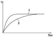
도 2는 메모리 셀 어레이 중 메모리 셀의 위치에 따라 메모리 셀에 인가되는 전압의 RC 딜레이를 나타내는 그래프이다.
도 3 내지 도 8은 본 발명의 일 실시 예에 따른 반도체 메모리 장치의 제조 방법을 설명하기 위한 소자의 단면도이다.
도 9 내지 도 14는 본 발명의 다른 예에 따른 반도체 메모리 장치의 제조 방법을 설명하기 위한 소자의 단면도이다.
도 15는 본 발명의 실시 예에 따른 메모리 시스템을 나타낸 구성도이다.
도 16은 본 발명의 실시 예에 따른 컴퓨팅 시스템을 나타내는 구성도이다.1 is a circuit diagram showing a semiconductor memory device according to an embodiment of the present invention.
2 is a graph illustrating an RC delay of a voltage applied to a memory cell according to a position of the memory cell in the memory cell array.
3 to 8 are cross-sectional views of devices for describing a method of manufacturing a semiconductor memory device in accordance with an embodiment of the present invention.
9 to 14 are cross-sectional views of devices for describing a method of manufacturing a semiconductor memory device according to another embodiment of the present invention.
15 is a configuration diagram illustrating a memory system according to an embodiment of the present invention.
16 is a block diagram illustrating a computing system according to an exemplary embodiment of the present invention.
이하, 첨부된 도면을 참조하여 본 발명의 바람직한 실시 예를 설명하기로 한다. 그러나, 본 발명은 이하에서 개시되는 실시 예에 한정되는 것이 아니라 서로 다른 다양한 형태로 구현될 수 있으며, 단지 본 실시 예는 본 발명의 개시가 완전하도록 하며 통상의 지식을 가진자에게 발명의 범주를 완전하게 알려주기 위해 제공되는 것이다.
Hereinafter, preferred embodiments of the present invention will be described with reference to the accompanying drawings. It should be understood, however, that the invention is not limited to the disclosed embodiments, but may be embodied in many different forms and should not be construed as limiting the scope of the invention to those skilled in the art It is provided to let you know completely.
도 1은 본 발명의 실시 예에 따른 반도체 메모리 장치를 나타내는 회로도이다.1 is a circuit diagram showing a semiconductor memory device according to an embodiment of the present invention.
도 1을 참조하면, 반도체 메모리 장치는 메모리 셀 블럭(100) 및 전압 공급 회로(200)를 포함한다.Referring to FIG. 1, a semiconductor memory device includes a
메모리 셀 블럭(100)은 다수의 비트라인들(BL)과 소스 라인(SL) 사이에 연결되는 다수의 메모리 스트링(ST)을 포함한다.The
메모리 스트링(ST)은 비트라인(BL)과 소스 라인(SL) 사이에 직렬로 연결된 드레인 셀렉트 트랜지스터(DST), 셀 스트링(C0 내지 Cn) 및 소스 셀렉트 트랜지스터(SST)를 포함한다. 셀 스트링은 드레인 셀렉트 트랜지스터(DST)와 소스 셀렉트 트랜지스터(SST) 사이에 직렬로 연결된 메모리 셀들(C0 내지 Cn)을 포함한다.The memory string ST includes a drain select transistor DST, a cell string C0 to Cn, and a source select transistor SST connected in series between the bit line BL and the source line SL. The cell string includes memory cells C0 to Cn connected in series between the drain select transistor DST and the source select transistor SST.
구체적으로, 드레인 셀렉트 트랜지스터(DST)는 비트라인(BL)과 셀 스트링(C0 내지 Cn) 사이에 연결되고, 드레인 셀렉트 라인(DSL)에 인가되는 전압에 따라 셀 스트링(C0 내지 Cn)을 비트라인(BL)과 연결시킨다. 메모리 셀들(C0 내지 Cn)은 워드라인들(WL0 내지 WLn)에 인가되는 전압들에 따라 동작한다. 소스 셀렉트 트랜지스터(SST)는 셀 스트링(C0 내지 Cn)과 소스 라인(SL) 사이에 연결되며, 소스 셀렉트 라인(SSL)에 인가되는 전압에 따라 셀 스트링(C0 내지 Cn)을 소스 라인(SL)과 연결시킨다.In detail, the drain select transistor DST is connected between the bit line BL and the cell strings C0 to Cn, and the cell strings C0 to Cn are bit lines according to voltages applied to the drain select line DSL. Connect with (BL). The memory cells C0 to Cn operate according to the voltages applied to the word lines WL0 to WLn. The source select transistor SST is connected between the cell strings C0 to Cn and the source line SL, and the cell strings C0 to Cn are connected to the source line SL according to a voltage applied to the source select line SSL. Connect with
전압 공급 회로(200)는 전압 생성부(210) 및 디코더(220)를 포함한다.The
전압 생성부(210)는 프로그램 동작, 독출 동작, 검증 동작 시 메모리 셀들(C0 내지 Cn)과 연결된 워드라인들(WL0 내지 WLn)에 인가되는 동작 전압들, 예를 들어 프로그램 전압(Vpgm), 독출 전압(Vread), 검증 전압(Vverify) 및 패스 전압(Vpass) 등을 생성한다.The
디코더(220)는 전압 생성부(210)에서 생성된 동작 전압들을 메모리 셀 블럭(100)의 워드라인들(WL0 내지 WLn)에 선택적으로 인가한다.The
상술한 반도체 메모리 장치의 메모리 셀들은 메모리 셀 블럭(100) 내의 위치에 따라 제1 메모리 셀 영역(A)과 제2 메모리 셀 영역(B)으로 정의된다. 제1 메모리 셀 영역(A)은 메모리 셀 블럭(100) 중 전압 공급 회로(200)와 인접한 곳에 위치한다. 또한, 제2 메모리 셀 영역(B)은 제1 메모리 셀 영역(A)을 제외한 나머지 영역이거나, 제1 메모리 셀 영역(A) 비해 상대적으로 전압 공급 회로(200)와 거리가 먼 영역이다. 즉, 제1 메모리 셀 영역(A)은 전압 공급 회로(200)가 배치된 반도체 기판과 제2 메모리 셀 영역(B) 사이에 배치된 영역이다.
The memory cells of the semiconductor memory device described above are defined as a first memory cell area A and a second memory cell area B according to positions in the
도 2는 메모리 셀 어레이 중 메모리 셀의 위치에 따라 메모리 셀에 인가되는 전압의 RC 딜레이를 나타내는 그래프이다.2 is a graph illustrating an RC delay of a voltage applied to a memory cell according to a position of the memory cell in the memory cell array.
도 2를 참조하면, 도 1에 도시된 제1 메모리 셀 영역(A)에 배치된 메모리 셀들과 제2 메모리 셀 영역(B)에 배치된 메모리 셀들에 동작 전압 인가 시 RC 딜레이 현상에 의해 전압 상승 속도가 다른것을 나타난다. 상술한 RC 딜레이 현상은 메모리 셀들과 전압 공급 회로와의 거리에 따라 워드라인의 길이가 서로 상이함으로써 발생하며, 메모리 셀들과 전압 공급 회로와의 거리가 멀수록 RC 딜레이 현상이 증가하는 것을 알 수 있다. 상술한 RC 딜레이 현상에 의해 프로그램 동작 시 제1 메모리 셀 영역(A)의 메모리 셀들의 문턱 전압이 제2 메모리 셀 영역(B)의 문턱 전압보다 높게 프로그램될 수 있다.Referring to FIG. 2, when an operating voltage is applied to the memory cells disposed in the first memory cell region A and the memory cells disposed in the second memory cell region B shown in FIG. 1, the voltage rises due to an RC delay phenomenon. The speed is different. The above-mentioned RC delay phenomenon is caused by the length of word lines being different from each other according to the distance between the memory cells and the voltage supply circuit, and the RC delay phenomenon increases as the distance between the memory cells and the voltage supply circuit increases. . Due to the RC delay, the threshold voltages of the memory cells of the first memory cell region A may be programmed to be higher than the threshold voltage of the second memory cell region B during the program operation.
본 발명에서는 상술한 문제점을 해결하기 위하여, 제1 메모리 셀 영역(A)의 게이트 라인들 사이에 형성되는 에어갭보다 제2 메모리 셀 영역(B)의 게이트 라인들 사이에 형성되는 에어갭의 임계 치수가 크도록 형성하여, 제2 메모리 셀 영역(B)의 유전율을 낮춰 RC 딜레이 현상을 감소시킨다.
In the present invention, in order to solve the above-mentioned problem, the threshold of the air gap formed between the gate lines of the second memory cell region B rather than the air gap formed between the gate lines of the first memory cell region A By forming a large dimension, the dielectric constant of the second memory cell region B is lowered to reduce the RC delay phenomenon.
도 3 내지 도 8은 본 발명의 실시 예에 따른 반도체 메모리 장치의 제조 방법을 설명하기 위한 소자의 단면도이다.3 to 8 are cross-sectional views of devices for describing a method of manufacturing a semiconductor memory device in accordance with an embodiment of the present invention.
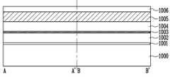
도 3을 참조하면, 도 1에 도시된 제1 메모리 셀 영역(A-A') 및 제2 메모리 셀 영역(B-B')이 정의된 반도체 기판(1000) 상에 터널 절연막(1001) 및 플로팅 게이트(floating gate)용 제1 도전막(1002)을 순차적으로 형성한다. 터널 절연막(1001)은 산화막으로 형성할 수 있으며, 제1 도전막(1002)은 폴리실리콘막으로 형성할 수 있다. 예를 들어, 제1 도전막(1002)은 불순물이 주입된 도프트(doped) 폴리실리콘막으로 형성하거나, 불순물이 주입되지 않은 언(undoped) 폴리실리콘막을 적층하여 형성할 수 있다. 이후 도면으로 도시되진 않았지만 통상적인 소자 분리 공정을 실시하여 소자 분리막을 형성할 수 있다.Referring to FIG. 3, a tunnel
이 후, 제1 도전막(1002) 상에 유전체막(1003), 콘트롤 게이트(control gate)용 제2 도전막(1004), 금속 게이트막(1005) 및 하드 마스크막(1006)을 순차적으로 적층하여 형성한다. 유전체막(1003)은 산화막, 질화막, 산화막이 순차적으로 적층된 ONO 구조로 형성하거나, 질화막 및 산화막을 순차적으로 적층하여 형성하거나, 고유전물질의 단층으로 형성할 수 있다. 제2 도전막(1004)은 폴리실리콘막으로 형성할 수 있으며, 예를 들면, 도프트 폴리실리콘막으로 형성할 수 있다. 금속 게이트막(1005)은 텅스텐막, 티타늄막, 코발트막, 금속 실리사이드막 등으로 형성할 수 있다. 하드 마스크막(1006)은 산화막 또는 질화막 또는 산화막과 질화막으로 이루어진 이중 구조막으로 형성할 수 있다.
After that, a
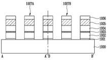
도 4를 참조하면, 패터닝 공정을 실시하여 제1 메모리 셀 영역(A-A') 상에 소자분리영역에 교차되는 방향으로 배열되는 제1 게이트 라인 패턴들(1007A)이 형성되고, 제2 메모리 셀 영역(B-B') 상에 소자분리영역에 교차되는 방향으로 배열되는 제2 게이트 라인 패턴들(1007B)이형성 된다.Referring to FIG. 4, a patterning process is performed to form first
제1 및 제2 게이트 라인 패턴(1007A, 1007B)들은 반도체 기판(1000) 상에 적층된 터널 절연막(1001), 제1 도전막(1002), 유전체막(1003), 제2 도전막(1004), 금속 게이트막(1005) 및 하드 마스크막(1006)으로 이루어진다.The first and second
이 후, 도면으로 도시되진 않았지만, 노출되는 소자분리영역의 소자 분리막 상단부를 식각하여 터널 절연막(1001)보다 소자 분리막의 상단부가 낮게 위치실 킬 수 있다. 이는 후속 에어갭 형성 공정시 에어갭이 터널 절연막(1001) 보다 낮은 위치까지 배치되도록 하기 위함이다.
Thereafter, although not shown in the drawings, the upper end of the device isolation layer of the exposed device isolation region may be etched so that the upper end of the isolation layer may be lower than the
도 5를 참조하면, 제1 및 제2 게이트 라인 패턴(1007A, 1007B)들을 포함한 전체 구조 상에 제1 절연막(1008)을 형성한다. 제1 절연막(1008)은 제1 및 제2 게이트 라인 패턴(1007A, 1007B)들 중 최 외각에 배치되는 선택 트랜지스터용 게이트 라인 패턴의 측벽에 형성되는 스페이서를 형성하기 위한 스페이서용 절연막일 수 있다. 제1 절연막(1008) 형성 공정시 게이트 라인 패턴들 사이의 공간이 좁아 게이트 라인 패턴들 사이의 공간이 완전히 매립되지 못한다. 이로 인하여 제1 게이트 라인 패턴(1007A) 사이의 공간에 제1 에어갭(A1)이 형성되고, 제2 게이트 라인 패턴(1007B) 사이의 공간에 제2 에어갭(A2)이 형성된다.
Referring to FIG. 5, the first insulating
도 6을 참조하면, 제1 게이트 라인 패턴들(1007A) 사이에 형성된 제1 에어갭(A1) 및 제2 게이트 라인 패턴들(1007B) 사이에 형성된 제2 에어갭(A2)이 노출되도록 에치백 공정을 실시한다. 이로 인하여 제1 및 제2 에어갭(A1, A2)의 상단부는 개구부를 갖는다. 상술한 에치백 공정은 제1 절연막(1008)을 식각하여 선택 트랜지스터용 게이트 라인 패턴의 측벽에 잔류시키기 위한 공정 일 수 있다
Referring to FIG. 6, the etch back is exposed to expose the first air gap A1 formed between the first
도 7을 참조하면, 제1 게이트 라인 패턴들(1007A)의 상부를 덮는 마스크 패턴(1009)을 형성한다. 마스크 패턴(1009)는 포토 레지스트로 형성할 수 있다.Referring to FIG. 7, a
이 후, 마스크 패턴(1009)에 의해 오픈된 제2 게이트 라인 패턴들(1007B) 사이의 공간에 개구부를 갖는 제2 에어갭(A2)의 크기를 증가시키기 위하여 식각 공정을 실시한다. 이로 인하여 제2 에어갭(A2)의 임계치수는 제1 에어갭(A1)의 임계치수보다 크게 형성된다.Thereafter, an etching process is performed to increase the size of the second air gap A2 having an opening in the space between the second
도 8을 참조하면, 마스크 패턴을 제거한 후, 노출된 제1 및 제2 에어갭(A1, A2)을 포함한 전체 구조 상에 제2 절연막(1010)을 형성한다. 이때 제2 절연막(1010)은 층간 절연막일 수 있다. 제2 절연막(1010)은 산화막으로 형성하는 것이 바람직하다.Referring to FIG. 8, after removing the mask pattern, the second insulating
제2 절연막(1010) 형성 공정 시 상단부가 노출되어 개구부를 갖던 제1 및 제2 에어갭(A1, A2)은 제2 절연막(1010)에 의해 개구부가 닫히게 된다.
In the process of forming the second insulating
상술한 바와 같이 본원 발명에 따르면, 게이트 라인들 사이의 공간에 에어갭이 형성되어 셀간 간섭 현상이 억제된다. 또한 전압 공급 회로와 상대적으로 거리가 가까운 제1 메모리 셀 영역(A)의 게이트 라인 패턴들 사이에 형성되는 에어갭보다 전압 공급 회로와 상대적으로 거리가 먼 제2 메모리 셀 영역(B)의 게이트 라인 패턴들 사이에 형성되는 에어갭의 임계 치수가 크도록 형성한다. 이로써 제2 메모리 셀 영역(B)에 배치된 게이트 라인 패턴들 간의 캐패시턴스가 낮아져 RC 딜레이 현상을 감소되며, 전압 공급 회로와의 거리에 따라 문턱 전압 분포가 변화되는 것이 억제된다.
As described above, according to the present invention, an air gap is formed in the space between the gate lines, thereby suppressing inter-cell interference. In addition, the gate line of the second memory cell region B is relatively far from the voltage supply circuit than the air gap formed between the gate line patterns of the first memory cell region A, which is relatively close to the voltage supply circuit. The critical dimension of the air gap formed between the patterns is formed to be large. As a result, the capacitance between the gate line patterns disposed in the second memory cell region B is lowered to reduce the RC delay, and the variation in the threshold voltage distribution according to the distance from the voltage supply circuit is suppressed.
도 9 내지 도 14는 본 발명의 다른 예에 따른 반도체 메모리 장치의 제조 방법을 설명하기 위한 소자의 단면도이다.9 to 14 are cross-sectional views of devices for describing a method of manufacturing a semiconductor memory device according to another embodiment of the present invention.
도 9를 참조하면, 도 1에 도시된 제1 메모리 셀 영역(A-A') 및 제2 메모리 셀 영역(B-B')이 정의된 반도체 기판(2000) 상에 터널 절연막(2001) 및 플로팅 게이트(floating gate)용 제1 도전막(2002)을 순차적으로 형성한다. 터널 절연막(2001)은 산화막으로 형성할 수 있으며, 제1 도전막(2002)은 폴리실리콘막으로 형성할 수 있다. 예를 들어, 제1 도전막(2002)은 불순물이 주입된 도프트(doped) 폴리실리콘막으로 형성하거나, 불순물이 주입되지 않은 언(undoped) 폴리실리콘막을 적층하여 형성할 수 있다. 이후 도면으로 도시되진 않았지만 통상적인 소자 분리 공정을 실시하여 소자 분리막을 형성할 수 있다.Referring to FIG. 9, a
이 후, 제1 도전막(2002) 상에 유전체막(2003), 콘트롤 게이트(control gate)용 제2 도전막(2004), 금속 게이트막(2005) 및 하드 마스크막(2006)을 순차적으로 적층하여 형성한다. 유전체막(2003)은 산화막, 질화막, 산화막이 순차적으로 적층된 ONO 구조로 형성하거나, 질화막 및 산화막을 순차적으로 적층하여 형성하거나, 고유전물질의 단층으로 형성할 수 있다. 제2 도전막(2004)은 폴리실리콘막으로 형성할 수 있으며, 예를 들면, 도프트 폴리실리콘막으로 형성할 수 있다. 금속 게이트막(2005)은 텅스텐막, 티타늄막, 코발트막, 금속 실리사이드막 등으로 형성할 수 있다. 하드 마스크막(2006)은 산화막 또는 질화막 또는 산화막과 질화막으로 이루어진 이중 구조막으로 형성할 수 있다.
After that, a
도 10을 참조하면, 패터닝 공정을 실시하여 제1 메모리 셀 영역(A-A') 상에 소자분리영역에 교차되는 방향으로 배열되는 제1 게이트 라인 패턴들(2007A)이 형성되고, 제2 메모리 셀 영역(B-B') 상에 소자분리영역에 교차되는 방향으로 배열되는 제2 게이트 라인 패턴들(2007B)이형성 된다.Referring to FIG. 10, first
제1 및 제2 게이트 라인 패턴(2007A, 2007B)들은 반도체 기판(2000) 상에 적층된 터널 절연막(2001), 제1 도전막(2002), 유전체막(2003), 제2 도전막(2004), 금속 게이트막(2005) 및 하드 마스크막(2006)으로 이루어진다.The first and second
이 후, 도면으로 도시되진 않았지만, 노출되는 소자분리영역의 소자 분리막 상단부를 식각하여 터널 절연막(2001)보다 소자 분리막의 상단부가 낮게 위치실 킬 수 있다. 이는 후속 에어갭 형성 공정시 에어갭이 터널 절연막(2001) 보다 낮은 위치까지 배치되도록 하기 위함이다.
Afterwards, although not shown in the drawings, the upper end of the device isolation layer of the exposed device isolation region may be etched to lower the upper end of the device isolation layer than the
도 11을 참조하면, 제1 및 제2 게이트 라인 패턴(2007A, 2007B)들을 포함한 전체 구조 상에 제1 절연막(2008)을 형성한다. 제1 절연막(2008)은 제1 및 제2 게이트 라인 패턴(2007A, 2007B)들 중 최 외각에 배치되는 선택 트랜지스터용 게이트 라인 패턴의 측벽에 형성되는 스페이서를 형성하기 위한 스페이서용 절연막일 수 있다. 제1 절연막(2008) 형성 공정시 게이트 라인 패턴들 사이의 공간이 좁아 게이트 라인 패턴들 사이의 공간이 완전히 매립되지 못한다. 이로 인하여 제1 게이트 라인 패턴(2007A) 사이의 공간에 제1 에어갭(A1)이 형성되고, 제2 게이트 라인 패턴(2007B) 사이의 공간에 제2 에어갭(A2)이 형성된다.
Referring to FIG. 11, the first insulating
도 12를 참조하면, 제1 게이트 라인 패턴들(2007A) 사이에 형성된 제1 에어갭(A1) 및 제2 게이트 라인 패턴들(2007B) 사이에 형성된 제2 에어갭(A2)이 노출되도록 에치백 공정을 실시한다. 이로 인하여 제1 및 제2 에어갭(A1, A2)의 상단부는 개구부를 갖는다. 상술한 에치백 공정은 제1 절연막(2008)을 식각하여 선택 트랜지스터용 게이트 라인 패턴의 측벽에 잔류시키기 위한 공정 일 수 있다
Referring to FIG. 12, the etch back is exposed to expose the first air gap A1 formed between the first
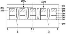
도 13을 참조하면, 제2 게이트 라인 패턴들(2007B)의 상부를 덮는 마스크 패턴(2009)을 형성한다. 마스크 패턴(2009)는 포토 레지스트로 형성할 수 있다.Referring to FIG. 13, a
이 후, 마스크 패턴(2009)에 의해 오픈된 제1 메모리 셀 영역(A-A')의 전체 구조를 따라 보조막(2010)을 형성한다. 보다 상세하게는, 제1 에어갭(A1)의 표면을 따라 보조막(2010)을 형성하여 제1 에어갭(A1)의 임계치수가 제2 에어갭(A2)의 임계치수 보다 작아지도록 한다.Thereafter, the
도 14를 참조하면, 마스크 패턴을 제거한 후, 노출된 제1 및 제2 에어갭(A1, A2)을 포함한 전체 구조 상에 제2 절연막(2011)을 형성한다. 이때 제2 절연막(2011)은 층간 절연막일 수 있다. 제2 절연막(2011)은 산화막으로 형성하는 것이 바람직하다.Referring to FIG. 14, after removing the mask pattern, the second insulating
제2 절연막(2011) 형성 공정 시 상단부가 노출되어 개구부를 갖던 제1 및 제2 에어갭(A1, A2)은 제2 절연막(2011)에 의해 개구부가 닫히게 된다.
In the process of forming the second insulating
상술한 바와 같이 본원 발명에 따르면, 게이트 라인들 사이의 공간에 에어갭이 형성되어 셀간 간섭 현상이 억제된다. 또한 전압 공급 회로와 상대적으로 거리가 가까운 제1 메모리 셀 영역(A)의 게이트 라인 패턴들 사이에 형성되는 에어갭보다 전압 공급 회로와 상대적으로 거리가 먼 제2 메모리 셀 영역(B)의 게이트 라인 패턴들 사이에 형성되는 에어갭의 임계 치수가 크도록 형성한다. 이로써 제2 메모리 셀 영역(B)에 배치된 게이트 라인 패턴들 간의 캐패시턴스가 낮아져 RC 딜레이 현상을 감소되며, 전압 공급 회로와의 거리에 따라 문턱 전압 분포가 변화되는 것이 억제된다.
As described above, according to the present invention, an air gap is formed in the space between the gate lines, thereby suppressing inter-cell interference. In addition, the gate line of the second memory cell region B is relatively far from the voltage supply circuit than the air gap formed between the gate line patterns of the first memory cell region A, which is relatively close to the voltage supply circuit. The critical dimension of the air gap formed between the patterns is formed to be large. As a result, the capacitance between the gate line patterns disposed in the second memory cell region B is lowered to reduce the RC delay, and the variation in the threshold voltage distribution according to the distance from the voltage supply circuit is suppressed.
도 15는 본 발명의 실시 예에 따른 메모리 시스템을 나타낸 구성도이다.15 is a configuration diagram illustrating a memory system according to an embodiment of the present invention.
도 15를 참조하면, 본 발명의 실시예에 따른 메모리 시스템(1100)은 반도체 메모리 장치(1120)와 메모리 컨트롤러(1110)를 포함한다.Referring to FIG. 15, a
반도체 메모리 장치(1120)는 도 1 및 도 3 내지 14에서 상술한 실시예들을 참조하여 설명한 반도체 메모리 장치를 포함한다. 또한, 반도체 메모리 장치(1120)는 복수의 플래시 메모리 칩들로 구성된 멀티-칩 패키지일 수 있다.The
메모리 컨트롤러(1110)는 반도체 메모리 장치(1120)를 제어하도록 구성되며, SRAM(1111), CPU(1112), 호스트 인터페이스(1113), ECC(1114), 메모리 인터페이스(1115)를 포함할 수 있다. SRAM(1111)은 CPU(1112)의 동작 메모리로 사용되고, CPU(1112)는 메모리 컨트롤러(1110)의 데이터 교환을 위한 제반 제어 동작을 수행하고, 호스트 인터페이스(1113)는 메모리 시스템(1100)과 접속되는 호스트의 데이터 교환 프로토콜을 구비한다. 또한, ECC(1114)는 반도체 메모리 장치(1120)로부터 리드된 데이터에 포함된 에러를 검출 및 정정하고, 메모리 인터페이스(1115)는 반도체 메모리 장치(1120)와의 인터페이싱을 수행한다. 이 밖에도 메모리 컨트롤러(1110)는 호스트와의 인터페이싱을 위한 코드 데이터를 저장하는 RCM 등을 더 포함할 수 있다.The
이와 같이, 구성을 갖는 메모리 시스템(1100)은 반도체 메모리 장치(1120)와 컨트롤러(1110)가 결합된 메모리 카드 또는 SSD(Solid State Disk)일 수 있다. 예를 들어, 메모리 시스템(1100)이 SSD인 경우, 메모리 컨트롤러(1110)는 USB, MMC, PCI-E, SATA, PATA, SCSI, ESDI, IDE 등과 같은 다양한 인터페이스 프로토콜들 중 하나를 통해 외부(예를 들어, 호스트)와 통신할 수 있다.
As described above, the
도 16은 본 발명의 실시 예에 따른 컴퓨팅 시스템을 나타내는 구성도이다.16 is a block diagram illustrating a computing system according to an exemplary embodiment of the present invention.
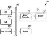
도 16을 참조하면, 본 발명의 실시예에 따른 컴퓨팅 시스템(1200)은 시스템 버스(1260)에 전기적으로 연결된 CPU(1220), RAM(1230), 유저 인터페이스(1240), 모뎀(1250), 메모리 시스템(1210)을 포함할 수 있다. 또한, 컴퓨팅 시스템(1200)이 모바일 장치인 경우, 컴퓨팅 시스템(1200)에 동작 전압을 공급하기 위한 베터리가 더 포함될 수 있으며, 응용 칩셋, 카메라 이미지 프로세서(CIS), 모바일 디렘 등이 더 포함될 수 있다.Referring to FIG. 16, a computing system 1200 according to an embodiment of the present invention may include a
메모리 시스템(1210)은 앞서 도 15를 참조하여 설명한 바와 같이, 반도체 메모리 장치(1212), 메모리 컨트롤러(1211)로 구성될 수 있다.
As described above with reference to FIG. 15, the
100 : 메모리 셀 블럭200 : 전압 공급 회로
210 : 전압 생성부220 : 디코더
1000 : 반도체 기판1001 : 터널 절연막
1002 : 제1 도전막1003 : 유전체막
1004 : 제2 도전막1005 : 금속 게이트막
1006 : 하드 마스크막1007A,1007B : 제1 및 제2 게이트 라인 패턴
1008 : 제1 절연막1009 : 마스크 패턴
1010 : 제2 절연막100: memory cell block 200: voltage supply circuit
210: voltage generator 220: decoder
1000: semiconductor substrate 1001: tunnel insulating film
1002: first conductive film 1003: dielectric film
1004: second conductive film 1005: metal gate film
1006:
1008: first insulating film 1009: mask pattern
1010: second insulating film
Claims (17)
Translated fromKorean상기 메모리 셀 블럭에 포함된 다수의 메모리 셀들의 게이트 라인들에 동작 전압을 인가하기 위한 전압 공급 회로를 포함하며,
상기 제1 메모리 셀 영역의 게이트 라인들 사이에 배치된 제1 에어갭의 크기가 상기 제2 메모리 셀 영역의 게이트 라인들 사이에 배치된 제2 에어갭의 크기보다 작은 반도체 메모리 장치.
A memory cell block formed on the first memory cell region and the second memory cell region defined in the semiconductor substrate;
A voltage supply circuit for applying an operating voltage to gate lines of a plurality of memory cells included in the memory cell block,
The size of the first air gap disposed between the gate lines of the first memory cell region is smaller than the size of the second air gap disposed between the gate lines of the second memory cell region.
상기 제1 메모리 셀 영역은 상기 메모리 셀 블럭 중 상기 전압 공급 회로와 인접한 영역이며, 상기 제2 메모리 셀 영역은 상기 메모리 셀 블럭 중 상기 제1 메모리 셀 영역을 제외한 영역인 반도체 메모리 장치.
The method of claim 1,
The first memory cell area is an area adjacent to the voltage supply circuit of the memory cell block, and the second memory cell area is an area excluding the first memory cell area of the memory cell block.
상기 제1 메모리 셀 영역이 상기 전압 공급 회로와 상기 제2 메모리 셀 영역 사이에 위치하는 반도체 메모리 장치.
The method of claim 1,
And the first memory cell region is located between the voltage supply circuit and the second memory cell region.
상기 전압 공급 회로는 상기 동작 전압을 생성하기 위한 전압 생성부; 및
상기 동작 전압을 상기 다수의 메모리 셀들의 게이트 라인들에 선택적으로 인가하기 위한 디코더를 포함하는 반도체 메모리 장치.
The method of claim 1,
The voltage supply circuit includes a voltage generator for generating the operating voltage; And
And a decoder for selectively applying the operating voltage to gate lines of the plurality of memory cells.
상기 제1 및 제2 에어갭의 크기에 따라 상기 제1 및 제2 메모리 셀 영역의 게이트 라인들의 RC 딜레이가 변화되는 반도체 메모리 장치.
The method of claim 1,
The RC delay of the gate lines of the first and second memory cell regions is changed according to the sizes of the first and second air gaps.
상기 제1 메모리 셀 영역 상에 형성된 상기 제1 게이트 라인 패턴들 사이의 공간에 제1 에어갭이 형성되고, 상기 제2 메모리 셀 영역 상에 형성된 상기 제2 게이트 라인 패턴들 사이의 공간에 제2 에어갭이 형성되도록 제1 절연막을 형성하는 단계; 및
상기 제2 에어갭의 임계치수를 증가시켜 상기 제1 에어갭의 임계치수보다 커지도록 상기 제2 메모리 셀 영역 상에 형성된 상기 제1 절연막을 선택적으로 식각하는 단계를 포함하는 반도체 메모리 장치의 제조 방법.
Forming first gate line patterns and second gate line patterns on a first memory cell region and a second memory cell region defined in a semiconductor substrate;
A first air gap is formed in the space between the first gate line patterns formed on the first memory cell region, and a second air gap is formed in the space between the second gate line patterns formed on the second memory cell region. Forming a first insulating film to form an air gap; And
Selectively etching the first insulating film formed on the second memory cell region so as to increase the threshold of the second air gap so as to be larger than the threshold of the first air gap. .
상기 제1 메모리 셀 영역은 메모리 셀 블럭이 형성되는 영역 중 메모리 셀들에 동작 전압을 인가하기 위한 전압 공급 회로와 인접한 영역이며, 상기 제2 메모리 셀 영역은 상기 메모리 셀 블럭이 형성되는 영역 중 상기 제1 메모리 셀 영역을 제외한 영역인 반도체 메모리 장치의 제조 방법.
The method according to claim 6,
The first memory cell area is an area adjacent to a voltage supply circuit for applying an operating voltage to memory cells among the areas where the memory cell block is formed, and the second memory cell area is the first area among the areas where the memory cell block is formed. 1 A method for manufacturing a semiconductor memory device which is an area excluding a memory cell area.
상기 제1 메모리 셀 영역이 메모리 셀들에 동작 전압을 인가하기 위한 전압 공급 회로와 상기 제2 메모리 셀 영역 사이에 위치하는 반도체 메모리 장치의 제조 방법.
The method according to claim 6,
And the first memory cell region is located between a voltage supply circuit for applying an operating voltage to the memory cells and the second memory cell region.
상기 제1 게이트 라인 패턴들 및 상기 제2 게이트 라인 패턴들을 형성하는 단계는
상기 반도체 기판 상에 터널 절연막, 도전막 및 하드 마스크막을 형성하는 단계;
상기 하드 마스크막, 상기 도전막 및 상기 터널 절연막을 패터닝하여 평행한 다수의 게이트 라인 패턴들을 형성하는 단계를 포함하는 반도체 메모리 장치의 제조 방법.
The method according to claim 6,
Forming the first gate line patterns and the second gate line patterns
Forming a tunnel insulating film, a conductive film, and a hard mask film on the semiconductor substrate;
Patterning the hard mask layer, the conductive layer, and the tunnel insulating layer to form a plurality of parallel gate line patterns.
상기 제1 절연막을 선택적으로 식각하는 단계는
상기 제1 및 제2 에어갭의 상단부가 노출되도록 상기 제1 절연막을 식각하는 단계;
상기 제1 메모리 셀 영역 상에 형성된 상기 제1 절연막을 덮고, 상기 제2 메모리 셀 영역 상에 형성된 상기 제1 절연막이 오픈되는 마스크 패턴을 형성하는 단계; 및
상기 제2 메모리 셀 영역 상에 상단부가 노출된 상기 제2 에어갭의 임계치수가 증가하도록 상기 제1 절연막을 식각하는 단계를 포함하는 반도체 메모리 장치의 제조 방법.
The method according to claim 6,
Selectively etching the first insulating layer
Etching the first insulating layer to expose upper ends of the first and second air gaps;
Forming a mask pattern covering the first insulating layer formed on the first memory cell region and opening the first insulating layer formed on the second memory cell region; And
And etching the first insulating layer to increase a critical dimension of the second air gap having an upper end exposed on the second memory cell region.
상기 제2 에어갭의 임계치수가 증가하도록 상기 제1 절연막을 식각하는 단계 이 후,
상기 마스크 패턴을 제거하는 단계; 및
상기 제1 및 제2 에어갭의 개구부가 덮혀지도록 상기 제1 절연막상에 제2 절연막을 형성하는 단계를 더 포함하는 반도체 메모리 소자의 제조 방법.
In the tenth,
After etching the first insulating layer to increase the critical dimension of the second air gap,
Removing the mask pattern; And
And forming a second insulating film on the first insulating film so that openings of the first and second air gaps are covered.
상기 제1 메모리 셀 영역 상에 형성된 상기 제1 게이트 라인 패턴들 사이의 공간에 제1 에어갭이 형성되고, 상기 제2 메모리 셀 영역 상에 형성된 상기 제2 게이트 라인 패턴들 사이의 공간에 제2 에어갭이 형성되도록 제1 절연막을 형성하는 단계; 및
상기 제1 에어갭의 임계치수를 감소시켜 상기 제2 에어갭의 임계치수보다 작아지도록 상기 제1 메모리 셀 영역 상에 형성된 상기 제1 에어갭의 내벽에 보조막을 형성하는 단계를 포함하는 반도체 메모리 장치의 제조 방법.
Forming first gate line patterns and second gate line patterns on a first memory cell region and a second memory cell region defined in a semiconductor substrate;
A first air gap is formed in the space between the first gate line patterns formed on the first memory cell region, and a second air gap is formed in the space between the second gate line patterns formed on the second memory cell region. Forming a first insulating film to form an air gap; And
Forming an auxiliary layer on an inner wall of the first air gap formed on the first memory cell region to reduce the threshold of the first air gap so as to be smaller than the threshold of the second air gap. Method of preparation.
상기 제1 메모리 셀 영역은 메모리 셀 블럭이 형성되는 영역 중 메모리 셀들에 동작 전압을 인가하기 위한 전압 공급 회로와 인접한 영역이며, 상기 제2 메모리 셀 영역은 상기 메모리 셀 블럭이 형성되는 영역 중 상기 제1 메모리 셀 영역을 제외한 영역인 반도체 메모리 장치의 제조 방법.
13. The method of claim 12,
The first memory cell area is an area adjacent to a voltage supply circuit for applying an operating voltage to memory cells among the areas where the memory cell block is formed, and the second memory cell area is the first area among the areas where the memory cell block is formed. 1 A method for manufacturing a semiconductor memory device which is an area excluding a memory cell area.
상기 제1 메모리 셀 영역이 메모리 셀들에 동작 전압을 인가하기 위한 전압 공급 회로와 상기 제2 메모리 셀 영역 사이에 위치하는 반도체 메모리 장치의 제조 방법.
13. The method of claim 12,
And the first memory cell region is located between a voltage supply circuit for applying an operating voltage to the memory cells and the second memory cell region.
상기 제1 게이트 라인 패턴들 및 상기 제2 게이트 라인 패턴들을 형성하는 단계는
상기 반도체 기판 상에 터널 절연막, 도전막 및 하드 마스크막을 형성하는 단계;
상기 하드 마스크막, 상기 도전막 및 상기 터널 절연막을 패터닝하여 평행한 다수의 게이트 라인 패턴들을 형성하는 단계를 포함하는 반도체 메모리 장치의 제조 방법.
13. The method of claim 12,
Forming the first gate line patterns and the second gate line patterns
Forming a tunnel insulating film, a conductive film, and a hard mask film on the semiconductor substrate;
Patterning the hard mask layer, the conductive layer, and the tunnel insulating layer to form a plurality of parallel gate line patterns.
상기 보조막을 형성하는 단계는
상기 제1 및 제2 에어갭의 상단부가 노출되도록 상기 제1 절연막을 식각하는 단계;
상기 제2 메모리 셀 영역 상에 형성된 상기 제1 절연막을 덮고, 상기 제1 메모리 셀 영역 상에 형성된 상기 제1 절연막이 오픈되는 마스크 패턴을 형성하는 단계; 및
상기 제2 에어갭의 임계치수보다 상기 제1 에어갭의 임계치수가 작아지도록 상단부가 노출된 상기 제1 에어갭의 표면을 따라 상기 보조막을 형성하는 단계를 포함하는 반도체 메모리 장치의 제조 방법.
13. The method of claim 12,
Forming the auxiliary film
Etching the first insulating layer to expose upper ends of the first and second air gaps;
Forming a mask pattern covering the first insulating layer formed on the second memory cell region and opening the first insulating layer formed on the first memory cell region; And
And forming the auxiliary layer along a surface of the first air gap, the upper end of which is exposed such that the critical dimension of the first air gap is smaller than the threshold of the second air gap.
상기 보조막을 형성하는 단계 이 후,
상기 마스크 패턴을 제거하는 단계; 및
상기 제1 및 제2 에어갭의 개구부가 덮혀지도록 상기 제1 절연막상에 제2 절연막을 형성하는 단계를 더 포함하는 반도체 메모리 소자의 제조 방법.
In the sixteenth,
After forming the auxiliary layer,
Removing the mask pattern; And
And forming a second insulating film on the first insulating film so that openings of the first and second air gaps are covered.
Priority Applications (2)
| Application Number | Priority Date | Filing Date | Title |
|---|---|---|---|
| KR1020120086881AKR20140020146A (en) | 2012-08-08 | 2012-08-08 | Semiconductor memory device and manufacturing method thereof |
| US13/605,243US20140043905A1 (en) | 2012-08-08 | 2012-09-06 | Semiconductor memory device and method of manufacturing the same |
Applications Claiming Priority (1)
| Application Number | Priority Date | Filing Date | Title |
|---|---|---|---|
| KR1020120086881AKR20140020146A (en) | 2012-08-08 | 2012-08-08 | Semiconductor memory device and manufacturing method thereof |
Publications (1)
| Publication Number | Publication Date |
|---|---|
| KR20140020146Atrue KR20140020146A (en) | 2014-02-18 |
Family
ID=50066090
Family Applications (1)
| Application Number | Title | Priority Date | Filing Date |
|---|---|---|---|
| KR1020120086881AWithdrawnKR20140020146A (en) | 2012-08-08 | 2012-08-08 | Semiconductor memory device and manufacturing method thereof |
Country Status (2)
| Country | Link |
|---|---|
| US (1) | US20140043905A1 (en) |
| KR (1) | KR20140020146A (en) |
Families Citing this family (3)
| Publication number | Priority date | Publication date | Assignee | Title |
|---|---|---|---|---|
| KR102402482B1 (en) | 2015-11-27 | 2022-05-25 | 삼성전자주식회사 | Semiconductor device and method for fabricating the same |
| US11508827B2 (en) | 2018-09-26 | 2022-11-22 | Taiwan Semiconductor Manufacturing Co., Ltd. | Air spacer for a gate structure of a transistor |
| US11121142B2 (en)* | 2019-12-31 | 2021-09-14 | Winbond Electronics Corp. | Memory structure and manufacturing method therefor |
Family Cites Families (5)
| Publication number | Priority date | Publication date | Assignee | Title |
|---|---|---|---|---|
| FR2803092B1 (en)* | 1999-12-24 | 2002-11-29 | St Microelectronics Sa | METHOD FOR PRODUCING ISOLATED METAL INTERCONNECTIONS IN INTEGRATED CIRCUITS |
| US20050232061A1 (en)* | 2004-04-16 | 2005-10-20 | Rust Thomas F | Systems for writing and reading highly resolved domains for high density data storage |
| KR100854498B1 (en)* | 2006-09-04 | 2008-08-26 | 삼성전자주식회사 | NAND type flash memory device comprising select transistors having impurity regions for punch-through suppression and a method of manufacturing the same |
| JP5788183B2 (en)* | 2010-02-17 | 2015-09-30 | 三星電子株式会社Samsung Electronics Co.,Ltd. | Nonvolatile memory device, method of operating the same, and memory system including the same |
| KR101762661B1 (en)* | 2010-09-17 | 2017-08-04 | 삼성전자주식회사 | Method of manufacturing a semiconductor device |
- 2012
- 2012-08-08KRKR1020120086881Apatent/KR20140020146A/ennot_activeWithdrawn
- 2012-09-06USUS13/605,243patent/US20140043905A1/ennot_activeAbandoned
Also Published As
| Publication number | Publication date |
|---|---|
| US20140043905A1 (en) | 2014-02-13 |
Similar Documents
| Publication | Publication Date | Title |
|---|---|---|
| US10546877B2 (en) | Semiconductor device and method of fabricating the same | |
| US10424590B2 (en) | Memory device and manufacturing method thereof | |
| US9842855B2 (en) | Manufacturing method of memory device | |
| US8116111B2 (en) | Nonvolatile memory devices having electromagnetically shielding source plates | |
| US9673218B1 (en) | Method of manufacturing semiconductor device including channel layer | |
| CN103515392A (en) | Semiconductor device and method of manufacturing the same | |
| US8946804B2 (en) | Semiconductor device and method of manufacturing the same | |
| US10347318B2 (en) | Semiconductor memory device | |
| KR20190019672A (en) | Semiconductor device and method of manufacturing the same | |
| US9490159B2 (en) | Semiconductor device and method of manufacturing the same | |
| US20110193151A1 (en) | Nonvolatile semiconductor memory device | |
| KR20150017600A (en) | Semiconductor memory device | |
| US9613972B1 (en) | Method of manufacturing semiconductor device | |
| KR20140018515A (en) | Semiconductor device and method of manufacturing the same | |
| US20210028188A1 (en) | Semiconductor memory device and manufacturing method of the semiconductor memory device | |
| US9390963B2 (en) | Semiconductor memory device | |
| KR20140020146A (en) | Semiconductor memory device and manufacturing method thereof | |
| CN115483223A (en) | Semiconductor memory device and method for manufacturing semiconductor memory device | |
| KR20090070534A (en) | Flash device and manufacturing method thereof | |
| US12245433B2 (en) | Semiconductor memory device and method of manufacturing the same | |
| KR102869691B1 (en) | Semiconductor memory device and manufacturing method thereof | |
| US7851304B2 (en) | Nonvolatile memory device and fabrication method | |
| KR20140017219A (en) | Method of manufacturing non-volatile memory device | |
| KR20090070709A (en) | Contact hole formation method of semiconductor device | |
| KR20140080657A (en) | Semiconductor memory device and manufacturing method of the same |
Legal Events
| Date | Code | Title | Description |
|---|---|---|---|
| PA0109 | Patent application | Patent event code:PA01091R01D Comment text:Patent Application Patent event date:20120808 | |
| PG1501 | Laying open of application | ||
| PC1203 | Withdrawal of no request for examination | ||
| WITN | Application deemed withdrawn, e.g. because no request for examination was filed or no examination fee was paid |