KR20140019699A - A flexible organic light emitting display device and the manufacturing method thereof - Google Patents
A flexible organic light emitting display device and the manufacturing method thereofDownload PDFInfo
- Publication number
- KR20140019699A KR20140019699AKR1020120086397AKR20120086397AKR20140019699AKR 20140019699 AKR20140019699 AKR 20140019699AKR 1020120086397 AKR1020120086397 AKR 1020120086397AKR 20120086397 AKR20120086397 AKR 20120086397AKR 20140019699 AKR20140019699 AKR 20140019699A
- Authority
- KR
- South Korea
- Prior art keywords
- layer
- flexible
- flexible substrate
- light emitting
- organic light
- Prior art date
- Legal status (The legal status is an assumption and is not a legal conclusion. Google has not performed a legal analysis and makes no representation as to the accuracy of the status listed.)
- Withdrawn
Links
- 238000004519manufacturing processMethods0.000titleclaimsabstractdescription19
- 239000000758substrateSubstances0.000claimsabstractdescription114
- 239000011521glassSubstances0.000claimsabstractdescription28
- 238000006303photolysis reactionMethods0.000claimsabstractdescription15
- 230000015843photosynthesis, light reactionEffects0.000claimsabstractdescription15
- 230000001678irradiating effectEffects0.000claimsabstractdescription4
- 229920000642polymerPolymers0.000claimsdescription41
- 230000004888barrier functionEffects0.000claimsdescription25
- 238000000034methodMethods0.000claimsdescription19
- 239000004642PolyimideSubstances0.000claimsdescription10
- 229920001721polyimidePolymers0.000claimsdescription10
- 230000005611electricityEffects0.000abstractdescription16
- 230000003068static effectEffects0.000abstractdescription16
- 238000000926separation methodMethods0.000abstractdescription9
- 238000001782photodegradationMethods0.000abstractdescription2
- 239000010409thin filmSubstances0.000description16
- 239000000178monomerSubstances0.000description10
- 238000005538encapsulationMethods0.000description9
- 230000008569processEffects0.000description7
- GTDPSWPPOUPBNX-UHFFFAOYSA-Nac1mqpvaChemical compoundCC12C(=O)OC(=O)C1(C)C1(C)C2(C)C(=O)OC1=OGTDPSWPPOUPBNX-UHFFFAOYSA-N0.000description6
- 239000010408filmSubstances0.000description6
- 238000007789sealingMethods0.000description5
- 230000035515penetrationEffects0.000description4
- 150000001408amidesChemical class0.000description3
- 150000004985diaminesChemical class0.000description3
- 230000009477glass transitionEffects0.000description3
- 239000000565sealantSubstances0.000description3
- 230000035939shockEffects0.000description3
- CBCKQZAAMUWICA-UHFFFAOYSA-N1,4-phenylenediamineChemical compoundNC1=CC=C(N)C=C1CBCKQZAAMUWICA-UHFFFAOYSA-N0.000description2
- VLDPXPPHXDGHEW-UHFFFAOYSA-N1-chloro-2-dichlorophosphoryloxybenzeneChemical compoundClC1=CC=CC=C1OP(Cl)(Cl)=OVLDPXPPHXDGHEW-UHFFFAOYSA-N0.000description2
- 230000005540biological transmissionEffects0.000description2
- 238000000354decomposition reactionMethods0.000description2
- 238000010586diagramMethods0.000description2
- GNOIPBMMFNIUFM-UHFFFAOYSA-Nhexamethylphosphoric triamideChemical compoundCN(C)P(=O)(N(C)C)N(C)CGNOIPBMMFNIUFM-UHFFFAOYSA-N0.000description2
- 239000000463materialSubstances0.000description2
- 238000000059patterningMethods0.000description2
- 230000035699permeabilityEffects0.000description2
- XLYOFNOQVPJJNP-UHFFFAOYSA-NwaterChemical compoundOXLYOFNOQVPJJNP-UHFFFAOYSA-N0.000description2
- YGYCECQIOXZODZ-UHFFFAOYSA-N4415-87-6Chemical compoundO=C1OC(=O)C2C1C1C(=O)OC(=O)C12YGYCECQIOXZODZ-UHFFFAOYSA-N0.000description1
- WVOLTBSCXRRQFR-SJORKVTESA-NCannabidiolic acidNatural productsOC1=C(C(O)=O)C(CCCCC)=CC(O)=C1[C@@H]1[C@@H](C(C)=C)CCC(C)=C1WVOLTBSCXRRQFR-SJORKVTESA-N0.000description1
- 238000005452bendingMethods0.000description1
- WVOLTBSCXRRQFR-DLBZAZTESA-McannabidiolateChemical compoundOC1=C(C([O-])=O)C(CCCCC)=CC(O)=C1[C@H]1[C@H](C(C)=C)CCC(C)=C1WVOLTBSCXRRQFR-DLBZAZTESA-M0.000description1
- 239000003795chemical substances by applicationSubstances0.000description1
- VKIRRGRTJUUZHS-UHFFFAOYSA-Ncyclohexane-1,4-diamineChemical compoundNC1CCC(N)CC1VKIRRGRTJUUZHS-UHFFFAOYSA-N0.000description1
- 230000008021depositionEffects0.000description1
- 230000006866deteriorationEffects0.000description1
- 230000002542deteriorative effectEffects0.000description1
- 230000004048modificationEffects0.000description1
- 238000012986modificationMethods0.000description1
- 238000006116polymerization reactionMethods0.000description1
Images


Classifications
- H—ELECTRICITY
- H10—SEMICONDUCTOR DEVICES; ELECTRIC SOLID-STATE DEVICES NOT OTHERWISE PROVIDED FOR
- H10K—ORGANIC ELECTRIC SOLID-STATE DEVICES
- H10K71/00—Manufacture or treatment specially adapted for the organic devices covered by this subclass
- H10K71/80—Manufacture or treatment specially adapted for the organic devices covered by this subclass using temporary substrates
- H—ELECTRICITY
- H10—SEMICONDUCTOR DEVICES; ELECTRIC SOLID-STATE DEVICES NOT OTHERWISE PROVIDED FOR
- H10K—ORGANIC ELECTRIC SOLID-STATE DEVICES
- H10K50/00—Organic light-emitting devices
- H10K50/80—Constructional details
- H—ELECTRICITY
- H10—SEMICONDUCTOR DEVICES; ELECTRIC SOLID-STATE DEVICES NOT OTHERWISE PROVIDED FOR
- H10K—ORGANIC ELECTRIC SOLID-STATE DEVICES
- H10K59/00—Integrated devices, or assemblies of multiple devices, comprising at least one organic light-emitting element covered by group H10K50/00
- H10K59/80—Constructional details
- H10K59/805—Electrodes
- H10K59/8051—Anodes
- H10K59/80516—Anodes combined with auxiliary electrodes, e.g. ITO layer combined with metal lines
- H—ELECTRICITY
- H10—SEMICONDUCTOR DEVICES; ELECTRIC SOLID-STATE DEVICES NOT OTHERWISE PROVIDED FOR
- H10K—ORGANIC ELECTRIC SOLID-STATE DEVICES
- H10K77/00—Constructional details of devices covered by this subclass and not covered by groups H10K10/80, H10K30/80, H10K50/80 or H10K59/80
- H10K77/10—Substrates, e.g. flexible substrates
- H10K77/111—Flexible substrates
- H—ELECTRICITY
- H10—SEMICONDUCTOR DEVICES; ELECTRIC SOLID-STATE DEVICES NOT OTHERWISE PROVIDED FOR
- H10K—ORGANIC ELECTRIC SOLID-STATE DEVICES
- H10K85/00—Organic materials used in the body or electrodes of devices covered by this subclass
- H10K85/60—Organic compounds having low molecular weight
- H10K85/615—Polycyclic condensed aromatic hydrocarbons, e.g. anthracene
- H10K85/621—Aromatic anhydride or imide compounds, e.g. perylene tetra-carboxylic dianhydride or perylene tetracarboxylic di-imide
- H—ELECTRICITY
- H10—SEMICONDUCTOR DEVICES; ELECTRIC SOLID-STATE DEVICES NOT OTHERWISE PROVIDED FOR
- H10K—ORGANIC ELECTRIC SOLID-STATE DEVICES
- H10K2102/00—Constructional details relating to the organic devices covered by this subclass
- H10K2102/301—Details of OLEDs
- H10K2102/351—Thickness
- H—ELECTRICITY
- H10—SEMICONDUCTOR DEVICES; ELECTRIC SOLID-STATE DEVICES NOT OTHERWISE PROVIDED FOR
- H10K—ORGANIC ELECTRIC SOLID-STATE DEVICES
- H10K59/00—Integrated devices, or assemblies of multiple devices, comprising at least one organic light-emitting element covered by group H10K50/00
- H10K59/10—OLED displays
- Y—GENERAL TAGGING OF NEW TECHNOLOGICAL DEVELOPMENTS; GENERAL TAGGING OF CROSS-SECTIONAL TECHNOLOGIES SPANNING OVER SEVERAL SECTIONS OF THE IPC; TECHNICAL SUBJECTS COVERED BY FORMER USPC CROSS-REFERENCE ART COLLECTIONS [XRACs] AND DIGESTS
- Y02—TECHNOLOGIES OR APPLICATIONS FOR MITIGATION OR ADAPTATION AGAINST CLIMATE CHANGE
- Y02E—REDUCTION OF GREENHOUSE GAS [GHG] EMISSIONS, RELATED TO ENERGY GENERATION, TRANSMISSION OR DISTRIBUTION
- Y02E10/00—Energy generation through renewable energy sources
- Y02E10/50—Photovoltaic [PV] energy
- Y02E10/549—Organic PV cells
- Y—GENERAL TAGGING OF NEW TECHNOLOGICAL DEVELOPMENTS; GENERAL TAGGING OF CROSS-SECTIONAL TECHNOLOGIES SPANNING OVER SEVERAL SECTIONS OF THE IPC; TECHNICAL SUBJECTS COVERED BY FORMER USPC CROSS-REFERENCE ART COLLECTIONS [XRACs] AND DIGESTS
- Y02—TECHNOLOGIES OR APPLICATIONS FOR MITIGATION OR ADAPTATION AGAINST CLIMATE CHANGE
- Y02P—CLIMATE CHANGE MITIGATION TECHNOLOGIES IN THE PRODUCTION OR PROCESSING OF GOODS
- Y02P70/00—Climate change mitigation technologies in the production process for final industrial or consumer products
- Y02P70/50—Manufacturing or production processes characterised by the final manufactured product
Landscapes
- Engineering & Computer Science (AREA)
- Manufacturing & Machinery (AREA)
- Physics & Mathematics (AREA)
- Optics & Photonics (AREA)
- Spectroscopy & Molecular Physics (AREA)
- Chemical & Material Sciences (AREA)
- Materials Engineering (AREA)
- Electroluminescent Light Sources (AREA)
Abstract
Translated fromKoreanDescription
Translated fromKorean본 발명은 플렉시블 유기 발광 표시 장치와 그 제조방법에 관한 것으로서, 특히 제조과정 중 캐리어 기판의 탈착 시에 디스플레이부가 손상을 입지 않도록 개선된 플렉시블 유기 발광 표시 장치 및 그 제조방법에 관한 것이다.BACKGROUND OF THE INVENTION 1. Field of the Invention The present invention relates to a flexible organic light emitting display device and a method of manufacturing the same, and more particularly, to a flexible organic light emitting display device and an improved method of preventing a display unit from being damaged when a carrier substrate is detached during a manufacturing process.
예컨대 유기 발광 표시 장치는 구동 특성상 박형화 및 플랙시블화가 가능하여 이에 대한 많은 연구가 이루어지고 있다.For example, the organic light emitting diode display may be thinned and flexible in view of its driving characteristics, and thus, many studies have been conducted.
그런데, 이 유기 발광 표시 장치는 수분의 침투에 의해 디스플레이부가 열화되는 특성이 있다. 따라서, 외부로부터의 수분 침투를 방지하기 위해 디스플레이부를 밀봉하여 보호해주는 봉지 구조를 필요로 한다.However, the organic light emitting diode display has a characteristic of deteriorating the display unit due to the penetration of moisture. Therefore, a sealing structure is required to seal and protect the display unit in order to prevent moisture penetration from the outside.
종래에는 이러한 봉지 구조로서, 디스플레이부가 형성된 글라스기판 위에 그와 동일한 글라스 재질의 봉지기판을 덮고, 글라스기판과 봉지기판 사이는 실런트(sealant)로 밀봉시키는 구조가 주로 채용되었다. 즉, 두껍고 단단한 글라스기판의 디스플레이부 주변에 자외선 경화제와 같은 실런트를 도포하고, 그 위에 역시 두껍고 단단한 봉지기판을 덮은 후 자외선을 조사하여 실런트를 경화시킴으로써 밀봉이 이루어지도록 한 것이다.Conventionally, as such an encapsulation structure, a structure in which a sealing substrate of the same glass material is covered on a glass substrate on which a display unit is formed, and a sealant is sealed between the glass substrate and the encapsulation substrate is mainly employed. That is, a sealant such as an ultraviolet curing agent is coated around the display unit of the thick and hard glass substrate, and the sealing is made by curing the sealant by irradiating ultraviolet rays after covering the thick and rigid encapsulating substrate thereon.
그러나, 이러한 일반적인 봉지 구조로는 최근 유기 발광 표시 장치에 요구되고 있는 유연한 벤딩(bending) 특성을 만족시킬 수 없다. 즉, 최근에는 벤딩 상태로도 설치할 수 있는 유연성을 가진 플렉시블 유기 발광 표시 장치가 요구되고 있는데, 상기와 같이 두껍고 단단한 글라스기판과 봉지기판을 사용하게 되면 그러한 요구를 충족시키기가 어렵다.However, such a general encapsulation structure cannot satisfy the flexible bending characteristic that is recently required for an organic light emitting display device. In other words, recently, a flexible organic light emitting display device having a flexibility that can be installed in a bent state is required. When such a thick and rigid glass substrate and an encapsulation substrate are used, it is difficult to meet such a requirement.
따라서, 이러한 문제를 해결하기 위해 글라스재질의 기판 대신에 폴리머와 같은 박막층을 이용하는 박막 봉지 구조가 제안된 바 있다. 이것은 글라스기판 위에 디스플레이부 및 그 디스플레이부를 위아래에서 감싸는 박막층을 각각 형성한 후, 나중에 글라스기판은 떼어냄으로써 유연한 박막층이 디스플레이부에 대한 밀봉 기능을 대신하도록 한 것이다. 즉, 글라스기판은 제조공정 상의 캐리어 기판의 역할만 하도록 하는 것이다.Therefore, in order to solve this problem, a thin film encapsulation structure using a thin film layer such as a polymer instead of a glass substrate has been proposed. This is to form a display unit and a thin film layer surrounding the display unit above and below the glass substrate, respectively, and later remove the glass substrate so that the flexible thin film layer replaces the sealing function for the display unit. In other words, the glass substrate is intended to serve only as a carrier substrate in the manufacturing process.
그런데 문제는, 이와 같이 박막 봉지 구조를 만들기 위해 글라스기판을 박막층으로부터 분리해낼 때 그 분리면에서 수 kV 이상의 정전기가 발생하는 경우가 빈발한다는 점이다. 이렇게 되면 자칫 내부의 디스플레이부가 정전기에 의해 손상을 입을 수도 있기 때문에, 이를 방지하기 위한 대책이 요구되고 있다.However, the problem is that when the glass substrate is separated from the thin film layer in order to make the thin film encapsulation structure, electrostatic charges of several kV or more are frequently generated on the separation surface. In this case, since the display part inside may be damaged by static electricity, measures to prevent this are required.
본 발명의 실시예는 유연한 박막 봉지 구조를 가지며, 제조 과정 중 정전기 발생에 의한 디스플레이부 손상의 위험도 줄일 수 있도록 개선된 플렉시블 유기 발광 표시 장치 및 그 제조방법을 제공한다.An embodiment of the present invention provides a flexible organic light emitting display device and a method of manufacturing the same, which have a flexible thin film encapsulation structure and which can reduce the risk of damage to a display unit due to static electricity during a manufacturing process.
본 발명의 실시예에 따른 플렉시블 유기 발광 표시 장치는 제1가요성 기판과, 상기 제1가요성 기판의 일면에 형성된 디스플레이부와, 상기 제1가요성 기판의 타면에 형성된 정전기 방지층 및, 상기 디스플레이부를 덮어주는 제2가요성 기판을 구비한다.A flexible organic light emitting diode display according to an exemplary embodiment of the present invention includes a first flexible substrate, a display unit formed on one surface of the first flexible substrate, an antistatic layer formed on the other surface of the first flexible substrate, and the display. And a second flexible substrate covering the portion.
상기 정전기 방지층은 결정질 ITO층을 포함할 수 있으며, 상기 결정질 ITO층은 두께는 200nm 이하일 수 있다.The antistatic layer may include a crystalline ITO layer, and the crystalline ITO layer may have a thickness of 200 nm or less.
상기 제1가요성 기판은 순차 적층된 제1폴리머층과 제1배리어층을 포함할 수 있으며, 상기 제2가요성 기판은 순차 적층된 제2배리어층과 제2폴리머층을 포함할 수 있다.The first flexible substrate may include a first polymer layer and a first barrier layer sequentially stacked, and the second flexible substrate may include a second barrier layer and a second polymer layer sequentially stacked.
상기 제1가요성 기판은 두께 0.1mm 이하의 글라스 기판을 포함할 수 있으며, 상기 제2가요성 기판은 순차 적층된 배리어층과 폴리머층을 포함할 수 있다.The first flexible substrate may include a glass substrate having a thickness of 0.1 mm or less, and the second flexible substrate may include a barrier layer and a polymer layer sequentially stacked.
또한, 본 발명의 실시예에 따른 플렉시블 유기 발광 표시 장치의 제조방법은, 캐리어 기판 상에 광분해층과 정전기 방지층을 차례로 형성하는 단계; 상기 정전기 방지층 위에 제1가요성 기판을 마련하는 단계; 상기 제1가요성 위에 디스플레이부를 형성하는 단계; 상기 디스플레이부를 제2가요성 기판으로 덮는 단계; 및, 광을 조사하여 상기 광분해층을 분해시키고 상기 캐리어 기판을 제거하는 단계;를 포함한다.In addition, a method of manufacturing a flexible organic light emitting display device according to an embodiment of the present invention includes the steps of sequentially forming a photolysis layer and an antistatic layer on a carrier substrate; Providing a first flexible substrate over the antistatic layer; Forming a display unit on the first flexibility; Covering the display unit with a second flexible substrate; And irradiating light to decompose the photolysis layer and to remove the carrier substrate.
상기 광분해층은 폴리이미드층을 포함할 수 있으며, 상기 폴리이미드층의 두께는 100nm 이하일 수 있다.The photolysis layer may include a polyimide layer, and the thickness of the polyimide layer may be 100 nm or less.
상기 정전기 방지층은 ITO층을 포함할 수 있으며, 상기 ITO층의 두께는 200nm 이하일 수 있다.The antistatic layer may include an ITO layer, and the thickness of the ITO layer may be 200 nm or less.
상기 ITO층은 상기 광의 조사 전에는 비정질 ITO층으로 있다가, 상기 광의 조사에 따라 결정질 ITO층으로 전환될 수 있다.The ITO layer may be an amorphous ITO layer before the light is irradiated, and may be converted into a crystalline ITO layer according to the light irradiation.
상기 제1가요성 기판은 순차 적층된 제1폴리머층과 제1배리어층을 포함할 수 있으며, 상기 제2가요성 기판은 순차 적층된 제2배리어층과 제2폴리머층을 포함할 수 있다.The first flexible substrate may include a first polymer layer and a first barrier layer sequentially stacked, and the second flexible substrate may include a second barrier layer and a second polymer layer sequentially stacked.
상기 제1가요성 기판은 두께 0.1mm 이하의 글라스 기판을 포함할 수 있으며, 상기 제2가요성 기판은 순차 적층된 배리어층과 폴리머층을 포함할 수 있다.The first flexible substrate may include a glass substrate having a thickness of 0.1 mm or less, and the second flexible substrate may include a barrier layer and a polymer layer sequentially stacked.
상기한 바와 같은 본 발명의 플렉시블 유기 발광 표시 장치 및 제조방법에 의하면 박막 봉지 구조를 갖게 되므로 플렉시블 유기 발광 표시 장치의 유연성을 크게 향상시킬 수 있으며, 동시에 제조 과정 중의 정전기 발생을 억제할 수 있어서 제품 손상의 위험도 크게 줄일 수 있다.According to the flexible organic light emitting display device and the manufacturing method of the present invention as described above has a thin film encapsulation structure can greatly improve the flexibility of the flexible organic light emitting display device, and at the same time can suppress the generation of static electricity during the manufacturing process damage the product Risk can be greatly reduced.
도 1은 본 발명의 일 실시예에 따른 플렉시블 유기 발광 표시 장치를 도시한 단면도이다.
도 2a 내지 도 2c는 도 1에 도시된 플렉시블 유기 발광 표시 장치의 제조 과정을 도시한 도면이다.
도 3은 본 발명의 다른 실시예에 따른 플렉시블 유기 발광 표시 장치를 도시한 단면도이다.
도 4a 내지 도 4c는 도 3에 도시된 플렉시블 유기 발광 표시 장치의 제조 과정을 도시한 도면이다.1 is a cross-sectional view illustrating a flexible organic light emitting display device according to an exemplary embodiment of the present invention.
2A through 2C are diagrams illustrating a manufacturing process of the flexible organic light emitting diode display illustrated in FIG. 1.
3 is a cross-sectional view illustrating a flexible organic light emitting diode display according to another exemplary embodiment of the present invention.
4A through 4C are diagrams illustrating a manufacturing process of the flexible organic light emitting diode display illustrated in FIG. 3.
이하, 첨부된 도면들을 참조하여 본 발명의 바람직한 실시예를 상세히 설명하면 다음과 같다.Hereinafter, preferred embodiments of the present invention will be described in detail with reference to the accompanying drawings.
도 1은 본 발명의 일 실시예에 따른 플렉시블 유기 발광 표시 장치(100)를 도시한 것으로, 상향 발광 타입을 예시한 것이다.1 illustrates a flexible organic light
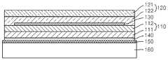
도시된 바와 같이 본 실시예의 플렉시블 유기 발광 표시 장치(100)는, 제1폴리머층(111)과 제1배리어층(112)을 포함한 제1가요성 기판(110)과, 박막트랜지스터(미도시)와 발광층(미도시) 등이 포함된 디스플레이부(130), 그리고 제2배리어층(122)과 제2폴리머층(121)을 포함한 제2가요성 기판(120)이 순차 적층된 구조로 이루어져 있다. 즉, 기존의 두껍고 단단한 글라스 기판을 대신하여 폴리머층(111,121)과 배리어층(112,122)으로 구성된 제1,2가요성 기판(110)(120)으로 디스플레이부(130)를 밀봉하는 봉지 구조를 구현하고 있다.As illustrated, the flexible organic light
그리고, 상기 제1가요성 기판(110)의 바깥 쪽 면에는 정전기 방지층(140)이 형성되어 있다. 상기 정전기 방지층(140)은 낮은 저항을 가진 결정질 ITO층이며, 이 정전기 방지층(140)이 디스플레이부(130)로 정전기 충격이 전달되는 것을 막아주게 된다. 상기 정전기 방지층(140)은 처음엔 비정질 ITO층으로 있다가, 제조과정 중에 조사되는 광을 흡수하면서 낮은 저항의 결정질로 전환된다. 이에 대한 자세한 제조과정은 후술하기로 한다.In addition, an
그리고, 상기 제1가요성 기판(110)의 제1폴리머층(111)은 유리전이온도가 500℃ 이상인 내열성 폴리이미드로 구성될 수 있으며, BPDA-biphenyl-tetracarboxylic acid dianhydride (3,3',4,4'-Biphenyl tetracarboxylic Dianhydride)와 p-phenylenediamine(PDA)의 중합에 의해 형성될 수 있다. 이 제1폴리머층(111)의 두께는 1~10㎛ 정도가 바람직하며, 이 위에 디스플레이부(130)가 적층되어 패터닝을 위한 수차례의 노광 공정을 거치게 되므로, 그 과정에서의 열화를 방지하려면 제1폴리머층(111)도 내열성이 높은 것을 사용하는 게 바람직하다. 이 제1폴리머층(111)이 기존의 글라스기판을 대신하는 하부 기판이 되며, 그 두께가 1~10㎛에 불과한 매우 유연한 박막 기판이 되는 것이다.In addition, the
다음으로, 상기 제1폴리머층(111) 위에 적층되는 제1배리어층(112)은 외부로부터의 수분의 침투를 막는 방습성을 가진 층으로서, 예컨대 SiO/SiN의 다층막으로 구성될 수 있다. 이것은 SiO와 SiN을 다층으로 적층한 것으로, 투습율(water vapor transmission rate)이 10-5 g/㎡·day 이하인 특성을 갖는다. 즉, 방습성이 우수하다. 이러한 제1배리어층(112)은 제1폴리머층(111) 위에 증착으로 형성될 수 있다.Next, the
다음으로, 디스플레이부(130) 위에 형성되는 제2가요성 기판(120)의 제2배리어층(122)은 외부로부터의 수분의 침투를 막는 방습성을 가진 층으로서, 예컨대 SiO/SiN의 다층막으로 구성될 수 있다. 이것은 SiO와 SiN을 다층으로 적층한 것으로, 투습율(water vapor transmission rate)이 10-5 g/㎡·day 이하인 특성을 갖는다. 즉, 방습성이 우수하다.Next, the
상기 제2배리어층(122) 위에 형성되는 제2폴리머층(121)은 유리전이온도가 350℃ 이상인 투명 폴리이미드로 구성될 수 있다. 상기 투명 폴리이미드는 이무수물계 단량체(dianhydride monomer)와, 디아민계 단량체(diamine monomer) 및, 아미드계 단량체(amide monomer) 중 하나 이상의 중합체일 수 있다. 예를 들어, 상기 투명 폴리이미드는 이무수물계 단량체와 디아민계 단량체의 중합체이거나, 이무수물계 단량체와 아미드계 단량체의 중합체일 수 있다. 상기 이무수물계 단량체의 비제한적인 예로는 pyromellitic dianhydride(PMDA), 1,2,3,4-cyclobutanetetracarboxylic dianhydride (CBDA) 등을 들 수 있다. 상기 디아민계 단량체의 비제한적인 예로는 trans-1,4-cyclohexanediamine (CHDA)을 들 수 있다. 상기 아미드계 단량체의 비제한적인 예로는 hexamethylphosphoramide (HMPA)를 들 수 있다. 본 실시예는 상향 발광 타입을 예시한 것이므로, 제2폴리머층(121) 측에서 디스플레이부(130)에서 구현된 화상을 볼 수 있어야 된다. 따라서, 제2폴리머층(121)은 디스플레이부(130)에서 구현된 화상을 투과시킬 수 있는 투명층이어야 한다. 그런데 투명한 폴리머의 경우에는 그렇지 않은 제1폴리머층(111)에 비해 내열성이 약간 떨어진다. 그러나, 제2폴리머층(121)은 제1폴리머층(111)처럼 디스플레이부(130)의 패터닝 공정을 함께 거치는 것이 아니기 때문에, 내열성이 조금 떨어지더라도 크게 문제될 것은 없다. 다만, 이후 캐리어 기판(160) 분리 시 자외선 노광을 거치게 되므로, 이때 해당 층에 문제가 생기지 않기 위해서는 유리전이온도 350℃ 이상은 필요하다. 물론, 이것은 제1폴리머층(111)에 비해 상대적으로 내열성이 낮다는 것이지, 절대적으로는 350℃의 온도를 견딜 수 있는 내열성 층이다.The
제2폴리머층(121)의 두께는 1~10㎛ 정도가 바람직하다. 이 제2폴리머층(121)이 기존의 글라스기판을 대신하는 상부 기판이 되며, 그 두께가 1~10㎛에 불과한 매우 유연한 박막 기판이 되는 것이다.The thickness of the
상기와 같은 구조의 플렉시블 유기 발광 표시 장치(100)는 다음과 같은 공정을 통해 제조될 수 있다.The flexible organic light emitting
우선, 도 2a에 도시된 바와 같이 글라스 재질의 캐리어 기판(160)을 준비하고 그 위에 박막층들을 형성한다.First, as shown in FIG. 2A, a
먼저, 캐리어 기판(160) 위에 폴리이미드층으로 구성된 광분해층(150)을 100nm 이하의 두께로 형성한다. 이것은 레이저광을 조사함에 따라 분해되는 층으로, 나중에 캐리어 기판(160)을 떼어내기 위해 제거되는 희생층이 된다.First, a
그리고, 광분해층(150) 위에 상기한 정전기 방지층(140)으로서 비정질 ITO층을 200nm 이하의 두께로 형성한다. 즉, 처음의 성막 단계에서는 정전기 방지층(140)의 ITO가 비정질 상태로 형성된다.An amorphous ITO layer is formed on the
이어서, 정전기 방지층(140) 위에 제1가요성 기판(110)의 제1폴리머층(111)과 제1배리어층(112)을 순차 형성한 후, 그 위에 디스플레이부(130)를 패터닝한다.Subsequently, the
그리고, 디스플레이부(130) 위에 제2가요성 기판(120)의 제2배리어층(122)과 제2폴리머층(121)을 순차 형성한다.In addition, the
이와 같은 과정으로 적층 구조가 만들어지면, 도 2b와 같이 캐리어 기판(160) 측에서 전면(全面)에 걸쳐 레이저광을 조사한다. 그러면, 상기 광분해층(150)은 레이저광에 의해 분해되기 시작하며, 상기 정전기 방지층(140)의 비정질 ITO는 레이저광을 흡수하여 저정항 특성의 결정질 ITO로 전환된다. 만일, 이 정전기 방지층(140)이 없다면, 레이저광이 디스플레이부(130)까지도 전달되어 박막트랜지스터나 발광층에도 손상을 입힐 수 있지만, 이 정전기 방지층(140)이 레이저광의 에너지를 흡수해주기 때문에 레이저광에 의한 직접적인 손상의 위험을 막아준다.When the laminated structure is formed by such a process, the laser beam is irradiated over the entire surface from the
이후에는 도 2c와 같이 상기 캐리어 기판(160)을 본체로부터 분리시키는데, 광분해층(150)의 분해가 완료됨에 따라 자연스럽게 캐리어 기판(160)이 본체로부터 떨어지게 된다. 이때, 상기 정전기 방지층(140)이 없다면, 캐리어 기판(160)과 제1폴리머층(111) 사이에 축적되어 있던 정전기가 상기와 같은 캐리어 기판(160)의 분리 작업 시 방전되면서 디스플레이부(130)에 손상을 입힐 수도 있지만, 본 구조에서는 저저항 특성의 결정질 ITO층으로 전환된 정전기 방지층(140)이 정전기가 축적되지 못하게 하므로, 이러한 문제가 해소될 수 있다. 즉, 상기 저저항 특성의 정전기 방지층(140)에 의해 정전기가 캐리어 기판(160)과 제1폴리머층(111) 사이에 축적되지 않고 분산되며, 이에 따라 캐리어 기판(160) 분리 시 분리면에 축적된 정전기가 일제히 방전되면서 수 kV 이상의 전기 충격이 디스플레이부(130)에 가해지는 현상이 방지되는 것이다.Thereafter, as shown in FIG. 2C, the
이렇게 제조된 유기 발광 표시 장치(100)에서는, 박막층인 제1,2가요성 기판(110)(120)이 기존의 단단하고 두꺼운 글라스 기판을 대신하기 때문에 유연성이 지닌 장치가 구현될 수 있다. 또한, 제1,2배리어층(112)(122)은 SiO/SiN의 다층막으로서 투습율이 10-5 g/㎡·day 이하이므로, 우수한 방습성도 확보할 수 있다.In the organic light emitting
또한, 정전기 방지층(140)에 의해 레이저광 조사 작업이나 캐리어 기판(160) 분리 작업 시에 디스플레이부(130)가 열 또는 정전기 충격에 의해 손상되는 문제도 해소할 수 있다. 그리고, 이 정전기 방지층(140)은 이후 제품의 사용 중에도 정전기가 축적되지 않게 해주므로, 사용 중의 정전기에 의한 손상도 방지해줄 수 있다.In addition, the problem that the
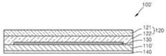
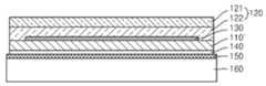
한편, 상기한 실시예에서는 제1,2가요성 기판(110)(120)을 모두 글라스가 아닌 재질로 형성하는 경우를 예시하였는데, 도 3에 도시된 다른 실시예의 구조와 같이 0.1mm 이하 두께의 얇은 글라스 기판을 제1가요성 기판(110')으로 사용할 수도 있다. 즉, 0.1mm 이하 두께인 글라스 기판은 글라스 재질임에도 불구하고 두께가 워낙 얇은 박판 구조라서 쉽게 휘어지는 유연성을 갖게 된다. 따라서, 제1가요성 기판(110')을 이 박판의 글라스 기판으로 대체하여 플렉시블 유기 발광 표시 장치(100')를 구현할 수도 있다.Meanwhile, in the above-described embodiment, all of the first and second
본 실시예의 플렉시블 유기 발광 표시 장치(100')는 다음과 같은 공정을 통해 제조될 수 있다.The flexible organic light emitting
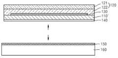
우선, 도 4a에 도시된 바와 같이 글라스 재질의 캐리어 기판(160)을 준비하고 그 위에 박막층들을 형성한다.First, as shown in FIG. 4A, a
먼저, 캐리어 기판(160) 위에 폴리이미드층으로 구성된 광분해층(150)을 100nm 이하의 두께로 형성한다. 이것은 레이저광을 조사함에 따라 분해되는 층으로, 나중에 캐리어 기판(160)을 떼어내기 위해 제거되는 희생층이 된다.First, a
그리고, 광분해층(150) 위에 상기한 정전기 방지층(140)으로서 비정질 ITO층을 200nm 이하의 두께로 형성한다. 즉, 처음의 성막 단계에서는 정전기 방지층(140)의 ITO가 비정질 상태로 형성된다.An amorphous ITO layer is formed on the
이어서, 정전기 방지층(140) 위에 제1가요성 기판(110')인 0.1mm 이하 두께의 글라스 기판을 설치한 후, 그 위에 디스플레이부(130)를 패터닝한다.Subsequently, a glass substrate having a thickness of 0.1 mm or less, which is the first
그리고, 디스플레이부(130) 위에 제2가요성 기판(120)의 배리어층(122)과 폴리머층(121)을 순차 형성한다.In addition, the
이와 같은 과정으로 적층 구조가 만들어지면, 도 4b와 같이 캐리어 기판(160) 측에서 전면(全面)에 걸쳐 레이저광을 조사한다. 그러면, 상기 광분해층(150)은 레이저광에 의해 분해되기 시작하며, 상기 정전기 방지층(140)의 비정질 ITO는 레이저광을 흡수하여 저정항 특성의 결정질 ITO로 전환된다. 만일, 이 정전기 방지층(140)이 없다면, 레이저광이 디스플레이부(130)까지도 전달되어 박막트랜지스터나 발광층에도 손상을 입힐 수 있지만, 이 정전기 방지층(140)이 레이저광의 에너지를 흡수해주기 때문에 레이저광에 의한 직접적인 손상의 위험을 막아준다.When the laminated structure is made by such a process, the laser beam is irradiated from the
이후에는 도 4c와 같이 상기 캐리어 기판(160)을 본체로부터 분리시키는데, 광분해층(150)의 분해가 완료됨에 따라 자연스럽게 캐리어 기판(160)이 본체로부터 떨어지게 된다. 이때, 상기 정전기 방지층(140)이 없다면, 캐리어 기판(160)과 제1가요성 기판(110') 사이에 축적되어 있던 정전기가 상기와 같은 캐리어 기판(160)의 분리 작업 시 방전되면서 디스플레이부(130)에 손상을 입힐 수도 있지만, 본 구조에서는 저저항 특성의 결정질 ITO층으로 전환된 정전기 방지층(140)이 정전기가 축적되지 못하게 하므로 이러한 문제가 해소될 수 있다. 즉, 상기 저저항 특성의 정전기 방지층(140)에 의해 정전기가 캐리어 기판(160)과 제1가요성 기판(110') 사이에 축적되지 않고 분산되며, 이에 따라 캐리어 기판(160) 분리 시 분리면에 축적된 정전기가 일제히 방전되면서 수 kV 이상의 전기 충격이 디스플레이부(130)에 가해지는 현상이 방지되는 것이다.Thereafter, as shown in FIG. 4C, the
본 실시예의 유기 발광 표시 장치(100')에서도, 매우 얇은 제1,2가요성 기판(110')(120)이 기존의 단단하고 두꺼운 글라스 기판을 대신하기 때문에 유연성을 지닌 장치가 구현될 수 있다. 또한, 제1,2배리어층(112)(122)은 SiO/SiN의 다층막으로서 투습율이 10-5 g/㎡·day 이하이므로, 우수한 방습성도 확보할 수 있다.In the organic light emitting
또한, 정전기 방지층(140)에 의해 레이저광 조사 작업이나 캐리어 기판(160) 분리 작업 시에 디스플레이부(130)가 열 또는 정전기 충격에 의해 손상되는 문제도 해소할 수 있다. 그리고, 이 정전기 방지층(140)은 이후 제품의 사용 중에도 정전기가 축적되지 않게 해주므로, 사용 중의 정전기에 의한 손상도 방지해줄 수 있다.In addition, the problem that the
본 발명은 첨부된 도면에 도시된 일 실시예를 참고로 설명되었으나 이는 예시적인 것에 불과하며, 당해 기술분야에서 통상의 지식을 가진 자라면 이로부터 다양한 변형 및 균등한 타 실시예가 가능하다는 점을 이해할 수 있을 것이다. 따라서 본 발명의 진정한 보호 범위는 첨부된 청구 범위에 의해서만 정해져야 할 것이다.While the present invention has been particularly shown and described with reference to exemplary embodiments thereof, it is clearly understood that the same is by way of illustration and example only and is not to be taken by way of limitation and that those skilled in the art will recognize that various modifications and equivalent arrangements may be made therein. It will be possible. Accordingly, the true scope of protection of the present invention should be determined only by the appended claims.
100,100'...플렉시블 유기 발광 표시 장치
110,110'...제1가요성 기판120...제2가요성 기판
111,121...제1,2폴리머층112,122...제1,2배리어층
130...디스플레이부 140...정전기 방지층
150...광분해층160...캐리어 기판100,100 '... flexible organic light emitting display
110,110 '... first
111,121 ... first and second polymer layers 112,122 ... first and second barrier layers
130
150 ...
Claims (13)
Translated fromKorean상기 제1가요성 기판의 일면에 형성된 디스플레이부와,
상기 제1가요성 기판의 타면에 형성된 정전기 방지층 및,
상기 디스플레이부를 덮어주는 제2가요성 기판을 구비하는 플렉시블 유기 발광 표시 장치.A first flexible substrate,
A display unit formed on one surface of the first flexible substrate,
An antistatic layer formed on the other surface of the first flexible substrate,
A flexible organic light emitting display device comprising a second flexible substrate covering the display unit.
상기 정전기 방지층은 결정질 ITO층을 포함하는 플렉시블 유기 발광 표시 장치.The method of claim 1,
The antistatic layer includes a crystalline ITO layer.
상기 결정질 ITO층은 두께가 200nm 이하인 플렉시블 유기 발광 표시 장치.3. The method of claim 2,
The crystalline ITO layer has a thickness of 200 nm or less.
상기 제1가요성 기판은 순차 적층된 제1폴리머층과 제1배리어층을 포함하며, 상기 제2가요성 기판은 순차 적층된 제2배리어층과 제2폴리머층을 포함하는 플렉시블 유기 발광 표시 장치.The method of claim 1,
The first flexible substrate includes a first polymer layer and a first barrier layer sequentially stacked, and the second flexible substrate includes a second barrier layer and a second polymer layer sequentially stacked. .
상기 제1가요성 기판은 두께 0.1mm 이하의 글라스 기판을 포함하며, 상기 제2가요성 기판은 순차 적층된 배리어층과 폴리머층을 포함하는 플렉시블 유기 발광 표시 장치.The method of claim 1,
The first flexible substrate includes a glass substrate having a thickness of 0.1 mm or less, and the second flexible substrate includes a barrier layer and a polymer layer that are sequentially stacked.
상기 정전기 방지층 위에 제1가요성 기판을 마련하는 단계;
상기 제1가요성 위에 디스플레이부를 형성하는 단계;
상기 디스플레이부를 제2가요성 기판으로 덮는 단계; 및,
광을 조사하여 상기 광분해층을 분해시키고 상기 캐리어 기판을 제거하는 단계;를 포함하는 플렉시블 유기 발광 표시 장치의 제조방법.Sequentially forming a photolysis layer and an antistatic layer on the carrier substrate;
Providing a first flexible substrate over the antistatic layer;
Forming a display unit on the first flexibility;
Covering the display unit with a second flexible substrate; And
Irradiating light to decompose the photolysis layer and to remove the carrier substrate.
상기 광분해층은 폴리이미드층을 포함하는 플렉시블 유기 발광 표시 장치의 제조방법.The method according to claim 6,
The photolysis layer manufacturing method of a flexible organic light emitting display device comprising a polyimide layer.
상기 폴리이미드층은 두께가 100nm 이하인 플렉시블 유기 발광 표시 장치의 제조방법.The method of claim 7, wherein
The polyimide layer has a thickness of 100nm or less manufacturing method of a flexible organic light emitting display device.
상기 정전기 방지층은 ITO층을 포함하는 플렉시블 유기 발광 표시 장치의 제조방법.The method according to claim 6,
The antistatic layer is a manufacturing method of a flexible organic light emitting display device including an ITO layer.
상기 ITO층은 상기 광의 조사 전에는 비정질 ITO층으로 있다가, 상기 광의 조사에 따라 결정질 ITO층으로 전환되는 플렉시블 유기 발광 표시 장치의 제조방법.The method of claim 9,
And the ITO layer is an amorphous ITO layer before the light is irradiated and is converted to a crystalline ITO layer in response to the light irradiation.
상기 ITO층은 두께가 200nm 이하인 플렉시블 유기 발광 표시 장치의 제조방법.The method of claim 9,
The ITO layer has a thickness of less than 200nm of a flexible organic light emitting display device manufacturing method.
상기 제1가요성 기판은 순차 적층된 제1폴리머층과 제1배리어층을 포함하며, 상기 제2가요성 기판은 순차 적층된 제2배리어층과 제2폴리머층을 포함하는 플렉시블 유기 발광 표시 장치의 제조방법.The method according to claim 6,
The first flexible substrate includes a first polymer layer and a first barrier layer sequentially stacked, and the second flexible substrate includes a second barrier layer and a second polymer layer sequentially stacked. Manufacturing method.
상기 제1가요성 기판은 두께 0.1mm 이하의 글라스 기판을 포함하며, 상기 제2가요성 기판은 순차 적층된 배리어층과 폴리머층을 포함하는 플렉시블 유기 발광 표시 장치의 제조방법.The method according to claim 6,
The first flexible substrate includes a glass substrate having a thickness of 0.1 mm or less, and the second flexible substrate includes a barrier layer and a polymer layer sequentially stacked.
Priority Applications (2)
| Application Number | Priority Date | Filing Date | Title |
|---|---|---|---|
| KR1020120086397AKR20140019699A (en) | 2012-08-07 | 2012-08-07 | A flexible organic light emitting display device and the manufacturing method thereof |
| US13/779,450US8815620B2 (en) | 2012-08-07 | 2013-02-27 | Flexible organic light-emitting display device and method of manufacturing the same |
Applications Claiming Priority (1)
| Application Number | Priority Date | Filing Date | Title |
|---|---|---|---|
| KR1020120086397AKR20140019699A (en) | 2012-08-07 | 2012-08-07 | A flexible organic light emitting display device and the manufacturing method thereof |
Publications (1)
| Publication Number | Publication Date |
|---|---|
| KR20140019699Atrue KR20140019699A (en) | 2014-02-17 |
Family
ID=50065514
Family Applications (1)
| Application Number | Title | Priority Date | Filing Date |
|---|---|---|---|
| KR1020120086397AWithdrawnKR20140019699A (en) | 2012-08-07 | 2012-08-07 | A flexible organic light emitting display device and the manufacturing method thereof |
Country Status (2)
| Country | Link |
|---|---|
| US (1) | US8815620B2 (en) |
| KR (1) | KR20140019699A (en) |
Cited By (2)
| Publication number | Priority date | Publication date | Assignee | Title |
|---|---|---|---|---|
| US10109695B2 (en) | 2015-09-25 | 2018-10-23 | Samsung Display Co., Ltd. | Flexible display panel with a conductive film in substrate layer |
| US12041810B2 (en) | 2019-12-31 | 2024-07-16 | Lg Display Co., Ltd. | Display device including rear surface metal deposition film |
Families Citing this family (10)
| Publication number | Priority date | Publication date | Assignee | Title |
|---|---|---|---|---|
| CN103426904B (en)* | 2013-08-02 | 2015-11-11 | 京东方科技集团股份有限公司 | A kind of flexible organic light emitting diode display and preparation method thereof |
| CN103681486B (en)* | 2013-12-06 | 2018-07-17 | 京东方科技集团股份有限公司 | A kind of manufacturing method of flexible display substrates |
| US9594287B2 (en)* | 2014-08-24 | 2017-03-14 | Royole Corporation | Substrate-less flexible display and method of manufacturing the same |
| KR102008766B1 (en)* | 2017-01-31 | 2019-08-09 | 주식회사 엘지화학 | Laminate for manufacturing flexible substrate and process for manufacturing flexible substrate using same |
| CN109427980B (en)* | 2017-08-24 | 2021-07-27 | 上海和辉光电股份有限公司 | Flexible display panel and flexible display device |
| WO2019059016A1 (en)* | 2017-09-19 | 2019-03-28 | 国立研究開発法人理化学研究所 | Electronic device and manufacturing method therefor |
| CN107768413B (en)* | 2017-10-26 | 2020-12-01 | 京东方科技集团股份有限公司 | A flexible display substrate, a display device and a manufacturing method thereof |
| WO2020232634A1 (en)* | 2019-05-21 | 2020-11-26 | 京东方科技集团股份有限公司 | Manufacturing method for flexible electronic substrate and substrate structure |
| US12207534B2 (en) | 2021-12-03 | 2025-01-21 | Wuhan China Star Optoelectronics Semiconductor Display Technology Co., Ltd. | Flexible display panel and manufacturing method thereof |
| CN114188498A (en)* | 2021-12-03 | 2022-03-15 | 武汉华星光电半导体显示技术有限公司 | Flexible display panel and preparation method thereof |
Family Cites Families (26)
| Publication number | Priority date | Publication date | Assignee | Title |
|---|---|---|---|---|
| TWI360702B (en) | 2003-03-07 | 2012-03-21 | Semiconductor Energy Lab | Liquid crystal display device and method for manuf |
| JP2004311955A (en)* | 2003-03-25 | 2004-11-04 | Sony Corp | Method for manufacturing very thin electro-optical display device |
| WO2005121908A1 (en)* | 2004-06-14 | 2005-12-22 | Semiconductor Energy Laboratory Co., Ltd. | Copy machine with copy control function, scanner and facsimile, and piece of paper and film each installed with semiconductor device |
| US7915058B2 (en)* | 2005-01-28 | 2011-03-29 | Semiconductor Energy Laboratory Co., Ltd. | Substrate having pattern and method for manufacturing the same, and semiconductor device and method for manufacturing the same |
| US7560789B2 (en)* | 2005-05-27 | 2009-07-14 | Semiconductor Energy Laboratory Co., Ltd. | Semiconductor device |
| KR101216125B1 (en)* | 2005-05-31 | 2012-12-27 | 가부시키가이샤 한도오따이 에네루기 켄큐쇼 | semiconductor device |
| WO2007055142A1 (en)* | 2005-11-11 | 2007-05-18 | Semiconductor Energy Laboratory Co., Ltd. | Layer having functionality, method for forming flexible substrate having the same, and method for manufacturing semiconductor device |
| US8222116B2 (en)* | 2006-03-03 | 2012-07-17 | Semiconductor Energy Laboratory Co., Ltd. | Method for manufacturing semiconductor device |
| US7713836B2 (en)* | 2006-09-29 | 2010-05-11 | Semiconductor Energy Laboratory Co., Ltd. | Method for forming conductive layer and substrate having the same, and method for manufacturing semiconductor device |
| KR100926222B1 (en) | 2007-12-28 | 2009-11-09 | 제일모직주식회사 | Polarizing film comprising an antistatic coating layer |
| WO2009104371A1 (en)* | 2008-02-20 | 2009-08-27 | シャープ株式会社 | Method for manufacturing flexible semiconductor substrate |
| KR100947435B1 (en) | 2008-03-25 | 2010-03-12 | 삼성모바일디스플레이주식회사 | Flexible display and manufacturing method thereof |
| KR101458901B1 (en)* | 2008-04-29 | 2014-11-10 | 삼성디스플레이 주식회사 | Manufacturing method of flexible display device |
| WO2009139282A1 (en)* | 2008-05-12 | 2009-11-19 | Semiconductor Energy Laboratory Co., Ltd. | Semiconductor device and method for manufacturing semiconductor device |
| WO2009148001A1 (en)* | 2008-06-06 | 2009-12-10 | Semiconductor Energy Laboratory Co., Ltd. | Method for manufacturing semiconductor device |
| US8053253B2 (en)* | 2008-06-06 | 2011-11-08 | Semiconductor Energy Laboratory Co., Ltd. | Method for manufacturing semiconductor device |
| KR101588576B1 (en)* | 2008-07-10 | 2016-01-26 | 가부시키가이샤 한도오따이 에네루기 켄큐쇼 | Light emitting device and electronic device |
| WO2010035627A1 (en)* | 2008-09-25 | 2010-04-01 | Semiconductor Energy Laboratory Co., Ltd. | Semiconductor device |
| JP5501174B2 (en)* | 2009-09-17 | 2014-05-21 | 株式会社半導体エネルギー研究所 | Semiconductor device |
| KR101617280B1 (en) | 2009-10-21 | 2016-05-03 | 엘지디스플레이 주식회사 | Methode of fabricating display device using flexible plastic substrate |
| JP2011138090A (en)* | 2010-01-04 | 2011-07-14 | Seiko Epson Corp | Substrate for electronic device, electronic device, method for manufacturing the same, and electronic apparatus |
| KR20180006507A (en)* | 2010-02-05 | 2018-01-17 | 가부시키가이샤 한도오따이 에네루기 켄큐쇼 | Semiconductor device and method for manufacturing the same |
| KR101172791B1 (en) | 2010-08-23 | 2012-08-09 | 주식회사 엘티에스 | Laser lift-off method and laser lift-off apparatus |
| US20130308076A1 (en)* | 2010-10-01 | 2013-11-21 | Sharp Kabushiki Kaisha | Flexible display and method for manufacturing the same |
| KR101174884B1 (en)* | 2010-12-23 | 2012-08-17 | 삼성디스플레이 주식회사 | A flexible organic light emitting display device and the manufacturing method thereof |
| CN102738078B (en)* | 2012-06-21 | 2014-11-12 | 京东方科技集团股份有限公司 | Method for manufacturing flexible display substrate |
- 2012
- 2012-08-07KRKR1020120086397Apatent/KR20140019699A/ennot_activeWithdrawn
- 2013
- 2013-02-27USUS13/779,450patent/US8815620B2/enactiveActive
Cited By (2)
| Publication number | Priority date | Publication date | Assignee | Title |
|---|---|---|---|---|
| US10109695B2 (en) | 2015-09-25 | 2018-10-23 | Samsung Display Co., Ltd. | Flexible display panel with a conductive film in substrate layer |
| US12041810B2 (en) | 2019-12-31 | 2024-07-16 | Lg Display Co., Ltd. | Display device including rear surface metal deposition film |
Also Published As
| Publication number | Publication date |
|---|---|
| US8815620B2 (en) | 2014-08-26 |
| US20140042399A1 (en) | 2014-02-13 |
Similar Documents
| Publication | Publication Date | Title |
|---|---|---|
| KR20140019699A (en) | A flexible organic light emitting display device and the manufacturing method thereof | |
| KR101174884B1 (en) | A flexible organic light emitting display device and the manufacturing method thereof | |
| KR101783781B1 (en) | A flat display device and the manufacturing method thereof | |
| US8466616B2 (en) | Flat panel display device and encapsulation substrate thereof | |
| EP3086381B1 (en) | Thin-film encapsulation structure for oled, oled device and display device | |
| TWI645593B (en) | Organic light emitting display device with flexible substrate | |
| US8093512B2 (en) | Package of environmentally sensitive electronic device and fabricating method thereof | |
| CN104037337B (en) | Organic electroluminescent display panel, packaging method thereof and display device | |
| KR101808535B1 (en) | Flexible Display Device and Method for Manufacturing the Same | |
| US9082999B2 (en) | Organic optoelectronic device and the encapsulation method thereof | |
| KR101454064B1 (en) | Organic light emitting device comprising encapsulating structure | |
| KR101511551B1 (en) | Organic Light Emitting Display Device and Method For Manufacturing the Same | |
| KR101086881B1 (en) | An organic light emitting display device having a light transmissive getter layer and a method of manufacturing the same | |
| JP7176954B2 (en) | ENCLOSING STRUCTURE, DISPLAY PANEL AND METHOD FOR MAKING THE SAME | |
| KR102222499B1 (en) | Organic light emitting display device | |
| KR20140137818A (en) | Adhesive Film and Organic Light Emitting Display Using The Same | |
| KR20160129778A (en) | Display module encapsulation structure and preparation method thereof | |
| US11659762B2 (en) | Flexible display panel and manufacturing method therefor, and flexible display apparatus | |
| KR20140067528A (en) | Display device, method of manufacturing display device and carrier glass | |
| JP6160107B2 (en) | Organic electroluminescence light emitting device, organic EL display device, and organic EL lighting | |
| KR20170050849A (en) | Organic light emitting display device and method for fabricating the same | |
| CN104183779A (en) | Filling film and method of manufacturing organic light-emitting display apparatus by using the same | |
| CN109037478B (en) | OLED packaging structure, OLED packaging method and display panel | |
| CN107731876A (en) | A kind of display panel and preparation method thereof, display device | |
| TWI707436B (en) | Package structure |
Legal Events
| Date | Code | Title | Description |
|---|---|---|---|
| PA0109 | Patent application | Patent event code:PA01091R01D Comment text:Patent Application Patent event date:20120807 | |
| PG1501 | Laying open of application | ||
| PC1203 | Withdrawal of no request for examination | ||
| WITN | Application deemed withdrawn, e.g. because no request for examination was filed or no examination fee was paid |