KR20140009287A - Conductive film and display apparatus provided with same - Google Patents
Conductive film and display apparatus provided with sameDownload PDFInfo
- Publication number
- KR20140009287A KR20140009287AKR1020137018810AKR20137018810AKR20140009287AKR 20140009287 AKR20140009287 AKR 20140009287AKR 1020137018810 AKR1020137018810 AKR 1020137018810AKR 20137018810 AKR20137018810 AKR 20137018810AKR 20140009287 AKR20140009287 AKR 20140009287A
- Authority
- KR
- South Korea
- Prior art keywords
- conductive
- conductive film
- patterns
- lattice
- gratings
- Prior art date
- Legal status (The legal status is an assumption and is not a legal conclusion. Google has not performed a legal analysis and makes no representation as to the accuracy of the status listed.)
- Ceased
Links
Images


Classifications
- G—PHYSICS
- G06—COMPUTING OR CALCULATING; COUNTING
- G06F—ELECTRIC DIGITAL DATA PROCESSING
- G06F3/00—Input arrangements for transferring data to be processed into a form capable of being handled by the computer; Output arrangements for transferring data from processing unit to output unit, e.g. interface arrangements
- G06F3/01—Input arrangements or combined input and output arrangements for interaction between user and computer
- G06F3/03—Arrangements for converting the position or the displacement of a member into a coded form
- G06F3/041—Digitisers, e.g. for touch screens or touch pads, characterised by the transducing means
- G06F3/044—Digitisers, e.g. for touch screens or touch pads, characterised by the transducing means by capacitive means
- G—PHYSICS
- G06—COMPUTING OR CALCULATING; COUNTING
- G06F—ELECTRIC DIGITAL DATA PROCESSING
- G06F3/00—Input arrangements for transferring data to be processed into a form capable of being handled by the computer; Output arrangements for transferring data from processing unit to output unit, e.g. interface arrangements
- G06F3/01—Input arrangements or combined input and output arrangements for interaction between user and computer
- G06F3/03—Arrangements for converting the position or the displacement of a member into a coded form
- G06F3/041—Digitisers, e.g. for touch screens or touch pads, characterised by the transducing means
- G06F3/0412—Digitisers structurally integrated in a display
- G—PHYSICS
- G06—COMPUTING OR CALCULATING; COUNTING
- G06F—ELECTRIC DIGITAL DATA PROCESSING
- G06F3/00—Input arrangements for transferring data to be processed into a form capable of being handled by the computer; Output arrangements for transferring data from processing unit to output unit, e.g. interface arrangements
- G06F3/01—Input arrangements or combined input and output arrangements for interaction between user and computer
- G06F3/03—Arrangements for converting the position or the displacement of a member into a coded form
- G06F3/041—Digitisers, e.g. for touch screens or touch pads, characterised by the transducing means
- G06F3/044—Digitisers, e.g. for touch screens or touch pads, characterised by the transducing means by capacitive means
- G06F3/0446—Digitisers, e.g. for touch screens or touch pads, characterised by the transducing means by capacitive means using a grid-like structure of electrodes in at least two directions, e.g. using row and column electrodes
- H—ELECTRICITY
- H05—ELECTRIC TECHNIQUES NOT OTHERWISE PROVIDED FOR
- H05K—PRINTED CIRCUITS; CASINGS OR CONSTRUCTIONAL DETAILS OF ELECTRIC APPARATUS; MANUFACTURE OF ASSEMBLAGES OF ELECTRICAL COMPONENTS
- H05K9/00—Screening of apparatus or components against electric or magnetic fields
- H—ELECTRICITY
- H05—ELECTRIC TECHNIQUES NOT OTHERWISE PROVIDED FOR
- H05K—PRINTED CIRCUITS; CASINGS OR CONSTRUCTIONAL DETAILS OF ELECTRIC APPARATUS; MANUFACTURE OF ASSEMBLAGES OF ELECTRICAL COMPONENTS
- H05K9/00—Screening of apparatus or components against electric or magnetic fields
- H05K9/0073—Shielding materials
- H05K9/0094—Shielding materials being light-transmitting, e.g. transparent, translucent
- H05K9/0096—Shielding materials being light-transmitting, e.g. transparent, translucent for television displays, e.g. plasma display panel
- G—PHYSICS
- G06—COMPUTING OR CALCULATING; COUNTING
- G06F—ELECTRIC DIGITAL DATA PROCESSING
- G06F2203/00—Indexing scheme relating to G06F3/00 - G06F3/048
- G06F2203/041—Indexing scheme relating to G06F3/041 - G06F3/045
- G06F2203/04103—Manufacturing, i.e. details related to manufacturing processes specially suited for touch sensitive devices
- G—PHYSICS
- G06—COMPUTING OR CALCULATING; COUNTING
- G06F—ELECTRIC DIGITAL DATA PROCESSING
- G06F2203/00—Indexing scheme relating to G06F3/00 - G06F3/048
- G06F2203/041—Indexing scheme relating to G06F3/041 - G06F3/045
- G06F2203/04112—Electrode mesh in capacitive digitiser: electrode for touch sensing is formed of a mesh of very fine, normally metallic, interconnected lines that are almost invisible to see. This provides a quite large but transparent electrode surface, without need for ITO or similar transparent conductive material
Landscapes
- Engineering & Computer Science (AREA)
- Physics & Mathematics (AREA)
- General Engineering & Computer Science (AREA)
- Theoretical Computer Science (AREA)
- Microelectronics & Electronic Packaging (AREA)
- Plasma & Fusion (AREA)
- Human Computer Interaction (AREA)
- General Physics & Mathematics (AREA)
- Position Input By Displaying (AREA)
- Devices For Indicating Variable Information By Combining Individual Elements (AREA)
- Shielding Devices Or Components To Electric Or Magnetic Fields (AREA)
Abstract
Translated fromKoreanDescription
Translated fromKorean본 발명은 도전성 필름 및 그것을 이용한 표시 디바이스 (장치) 에 관한 것이다.The present invention relates to a conductive film and a display device (apparatus) using the same.
표시 디바이스의 표시 패널 위에 배치되는 도전성 필름은, 도전성 전자파 실드 필름들 (예를 들어, 일본 공개특허공보 제 2008-282924호 및 제 2009-094467호 참조), 도전성 터치 패널 필름들 (예를 들어, 일본 공개특허공보 제 2010-108877호 참조) 등을 포함한다.The conductive film disposed on the display panel of the display device includes conductive electromagnetic shield films (see, for example, Japanese Patent Laid-Open Nos. 2008-282924 and 2009-094467), conductive touch panel films (for example, Japanese Unexamined Patent Publication No. 2010-108877) and the like.
이러한 도전성 필름들에서는, 격자 패턴이 투명 기판 상에 형성된다. 일본 공개특허공보 제 2008-282924호에서는, 모아레 (moire) 억제부가 격자 패턴의 교차부에 인접하여 배열된다. 일본 공개특허공보 제 2009-094467호에서는, 모아레 억제부를 갖는 모아레 억제 필름이 격자 패턴을 갖는 전자파 실드 필름에 부착되어 모아레 발생을 억제한다.In such conductive films, a lattice pattern is formed on the transparent substrate. In Japanese Laid-Open Patent Publication No. 2008-282924, a moire suppressor is arranged adjacent to the intersection of the lattice patterns. In Unexamined-Japanese-Patent No. 2009-094467, the moire suppression film which has a moire suppression part adheres to the electromagnetic shielding film which has a lattice pattern, and suppresses moire generation.
본 발명의 목적은, 상기 특허 문헌들의 구조들과 상이한 단순 구조를 가질 수 있고, 모아레 발생을 억제하면서 통상의 표시 디바이스의 표시 패널에 부착될 수 있으며, 그리고 고수율로 제조될 수 있는 도전성 필름을 제공하고, 그리고 도전성 필름을 갖는 표시 디바이스를 제공하는 것이다.An object of the present invention is to provide a conductive film which can have a simple structure different from the structures of the above patent documents, can be attached to a display panel of a conventional display device while suppressing moir generation, and can be manufactured in high yield. It is providing a display device having a conductive film.
[1] 기판 및 그 일 주면 상에 배치된 도전부를 포함하는 본 발명의 제 1 양태에 따른 도전성 필름으로서, 도전부는 금속 세선으로 구성되는 2 이상의 도전 패턴들을 포함하고, 도전 패턴들은 제 1 방향으로 연장되고 제 1 방향과 직교하는 제 2 방향으로 배열되고, 도전 패턴들은 각각 2 이상의 격자들의 조합을 포함하고, 격자들은 각각 마름모꼴 (rhombic) 형상을 가지며, 그리고 각 격자의 적어도 일 측변이 제 1 방향에 대해 30° ~ 90°의 각도인, 도전성 필름.[1] A conductive film according to the first aspect of the present invention comprising a substrate and a conductive portion disposed on one main surface thereof, wherein the conductive portion includes two or more conductive patterns composed of fine metal wires, and the conductive patterns are arranged in a first direction. Extending in a second direction orthogonal to the first direction, the conductive patterns each comprising a combination of two or more gratings, the gratings each having a rhombic shape, and at least one side of each grating being in the first direction The conductive film which is an angle of 30 degrees to 90 degrees with respect to.
[2] 제 1 양태에서, 각 격자의 적어도 일 측변이 제 1 방향에 대해 30° ~ 44°인 것이 바람직하다.[2] In the first aspect, it is preferable that at least one side of each grating is 30 ° to 44 ° with respect to the first direction.
[3] 제 1 양태에서, 각 격자의 적어도 일 측변이 제 1 방향에 대해 32° ~ 39°인 것이 바람직하다.[3] In the first aspect, it is preferable that at least one side of each grating is 32 ° to 39 ° with respect to the first direction.
[4] 제 1 양태에서, 각 격자의 적어도 일 측변이 제 1 방향에 대해 46° ~ 60°인 것이 바람직하다.[4] In the first aspect, it is preferable that at least one side of each grating is 46 ° to 60 ° with respect to the first direction.
[5] 제 1 양태에서, 각 격자의 적어도 일 측변이 제 1 방향에 대해 51° ~ 58°인 것이 바람직하다.[5] In the first aspect, it is preferable that at least one side of each grating is 51 ° to 58 ° with respect to the first direction.
[6] 제 1 양태에서, 도전 패턴들은 각각 제 1 방향으로 직렬로 접속되는 2 이상의 감지부들을 포함할 수도 있고, 그리고 감지부들은 각각 2 이상의 격자들의 조합을 포함할 수도 있다.[6] In the first aspect, the conductive patterns may each include two or more sensing units connected in series in a first direction, and the sensing units may each include a combination of two or more gratings.
[7] 기판, 기판의 일 주면 상에 배치된 제 1 도전부, 및 기판의 다른 주면 상에 배치된 제 2 도전부를 포함하는 본 발명의 제 2 양태에 따른 도전성 필름으로서, 제 1 도전부는 2 이상의 제 1 도전 패턴들을 포함하고, 제 1 도전 패턴들은 제 1 방향으로 연장되고 제 1 방향과 직교하는 제 2 방향으로 배열되고, 제 2 도전부는 2 이상의 제 2 도전 패턴들을 포함하고, 제 2 도전 패턴들은 제 2 방향으로 연장되고 제 1 방향으로 배열되고, 제 1 도전 패턴들 및 제 2 도전 패턴들은 각각 2 이상의 격자들의 조합을 포함하고, 격자들은 각각 마름모꼴 (rhombic) 형상을 가지며, 그리고 각 격자의 적어도 일 측변이 제 1 방향에 대해 30° ~ 60°의 각도인, 도전성 필름.[7] A conductive film according to the second aspect of the present invention, comprising a substrate, a first conductive portion disposed on one main surface of the substrate, and a second conductive portion disposed on the other main surface of the substrate, wherein the first conductive portion is formed of 2 Wherein the first conductive patterns include the first conductive patterns, wherein the first conductive patterns extend in a first direction and are arranged in a second direction perpendicular to the first direction, and the second conductive portion includes two or more second conductive patterns, and the second conductive pattern The patterns extend in a second direction and are arranged in a first direction, the first conductive patterns and the second conductive patterns each comprising a combination of two or more gratings, each grating having a rhombic shape, and each grating At least one side of the conductive film is an angle of 30 ° to 60 ° with respect to the first direction.
[8] 제 2 양태에서, 제 1 도전 패턴들은 각각 제 1 방향으로 직렬로 접속되는 2 이상의 제 1 감지부들을 포함할 수도 있고, 제 2 도전 패턴들은 각각 제 2 방향으로 직렬로 접속되는 2 이상의 제 2 감지부들을 포함할 수도 있으며, 그리고 제 1 감지부들 및 제 2 감지부들은 각각 2 이상의 격자들의 조합을 포함할 수도 있다.[8] In the second aspect, the first conductive patterns may each include two or more first sensing portions connected in series in a first direction, and the second conductive patterns are each two or more connected in series in a second direction. It may include second sensing units, and each of the first sensing units and the second sensing units may include a combination of two or more gratings.
[9] 기판 및 기판의 일 주면 상에 배치된 도전부를 포함하는 본 발명의 제 3 양태에 따른 도전성 필름으로서, 도전부는 개구부를 갖는 메시 패턴을 포함하고, 그리고 개구부는 각도가 60° ~ 120°인 마름모꼴 형상을 갖는, 도전성 필름.[9] A conductive film according to the third aspect of the present invention, comprising a substrate and a conductive portion disposed on one main surface of the substrate, wherein the conductive portion includes a mesh pattern having an opening, and the opening has an angle of 60 ° to 120 °. Electroconductive film which has a rhombic shape.
[10] 기판 및 기판의 일 주면 상에 배치된 도전부를 포함하는 본 발명의 제 4 양태에 따른 도전성 필름으로서, 도전부는 금속 세선으로 구성되는 2 이상의 도전 패턴들을 포함하고, 도전 패턴들은 제 1 방향으로 연장되고 제 1 방향과 직교하는 제 2 방향으로 배열되고, 도전 패턴들은 각각 제 1 방향으로 접속되는 2 이상의 감지부들을 포함하고, 그리고 감지부들 각각은 제 2 방향 길이 Lv 및 제 1 방향 길이 Lh 를 가지고, 0.57<Lv/Lh<1.74 의 조건을 만족하는, 도전성 필름.[10] A conductive film according to the fourth aspect of the present invention, comprising a substrate and a conductive portion disposed on one main surface of the substrate, wherein the conductive portion includes two or more conductive patterns composed of fine metal wires, and the conductive patterns are formed in a first direction. Extending in the second direction orthogonal to the first direction, the conductive patterns each including two or more sensing parts connected in the first direction, and each of the sensing parts has a second direction length Lv and a first direction length Lh. The conductive film which has a condition and satisfy | fills the conditions of 0.57 <Lv / Lh <1.74.
[11] 제 4 양태에서, 각 감지부는 0.57<Lv/Lh<1.00 의 조건을 만족하는 것이 바람직하다.[11] In the fourth aspect, each sensing unit preferably satisfies a condition of 0.57 <Lv / Lh <1.00.
[12] 기판, 기판의 일 주면 상에 배치된 제 1 도전부, 및 기판의 다른 주면 상에 배치된 제 2 도전부를 포함하는 본 발명의 제 5 양태에 따른 도전성 필름으로서, 제 1 도전부는 2 이상의 제 1 도전 패턴들을 포함하고, 제 1 도전 패턴들은 제 1 방향으로 연장되고 제 1 방향과 직교하는 제 2 방향으로 배열되고, 제 2 도전부는 2 이상의 제 2 도전 패턴들을 포함하고, 제 2 도전 패턴들 각각은 제 2 방향으로 연장되고 제 1 방향으로 배열되고, 제 1 도전 패턴들 각각은 제 1 방향으로 접속된 2 이상의 제 1 감지부들을 포함하고, 제 2 도전 패턴들 각각은 제 2 방향으로 접속된 2 이상의 제 2 감지부들을 포함하고, 제 1 감지부들 각각은 제 2 방향 길이 Lva 및 제 1 방향 길이 Lha 를 가지고, 0.57<Lva/Lha<1.74 의 조건을 만족하며, 그리고 제 2 감지부들 각각은 제 2 방향 길이 Lvb 및 제 1 방향 길이 Lhb 를 가지고, 0.57<Lvb/Lhb<1.74 의 조건을 만족하는, 도전성 필름.[12] A conductive film according to a fifth aspect of the present invention, comprising a substrate, a first conductive portion disposed on one main surface of the substrate, and a second conductive portion disposed on the other main surface of the substrate, wherein the first conductive portion is formed of 2 Wherein the first conductive patterns include the first conductive patterns, wherein the first conductive patterns extend in a first direction and are arranged in a second direction perpendicular to the first direction, and the second conductive portion includes two or more second conductive patterns, and the second conductive pattern Each of the patterns extends in a second direction and is arranged in a first direction, each of the first conductive patterns includes two or more first sensing units connected in a first direction, and each of the second conductive patterns is in a second direction. 2 or more second sensing units connected to each other, each of the first sensing units having a second direction length Lva and a first direction length Lha, satisfying a condition of 0.57 <Lva / Lha <1.74, and a second sensing unit Each of the parts has a second direction length Lvb and 1 has a length direction Lhb, 0.57 <Lvb / Lhb <satisfying the condition of 1.74, the conductive film.
[13] 제 5 양태에서, 각각의 제 1 감지부가 0.57<Lva/Lha<1.00 의 조건을 만족하고, 그리고 각각의 제 2 감지부가 0.57<Lvb/Lhb<1.00 의 조건을 만족하는 것이 바람직하다.[13] In the fifth aspect, it is preferable that each first sensing unit satisfies the condition of 0.57 <Lva / Lha <1.00, and each second sensing unit satisfies the condition of 0.57 <Lvb / Lhb <1.00.
[14] 제 4 양태 또는 제 5 양태에서, 감지부들 각각이 복수의 격자들을 포함하고, 그리고 각각의 격자가 제 2 방향 길이 Lvs 및 제 1 방향 길이 Lhs 를 가지고 0.57<Lvs/Lhs<1.74 의 조건을 만족하는 것이 바람직하다.[14] In the fourth or fifth aspect, each of the sensing parts includes a plurality of gratings, and each grating has a second direction length Lvs and a first direction length Lhs, wherein the condition of 0.57 <Lvs / Lhs <1.74 It is desirable to satisfy.
[15] 기판 및 기판의 일 주면 상에 배치된 도전부를 포함하는 본 발명의 제 6 양태에 따른 도전성 필름으로서, 도전부는 개구부를 갖는 메시 패턴을 포함하고, 개구부는 마름모꼴 형상을 가지며, 그리고 마름모꼴 형상은 하나의 대각선 길이 Lvp, 다른 대각선 길이를 Lhp 를 가지고, 0.57<Lvp/Lhp<1.74 의 조건을 만족하는, 도전성 필름.[15] A conductive film according to the sixth aspect of the present invention comprising a substrate and a conductive portion disposed on one main surface of the substrate, wherein the conductive portion includes a mesh pattern having an opening, the opening has a rhombic shape, and the rhombic shape Silver has one diagonal length Lvp, the other diagonal length Lhp, and satisfies the condition of 0.57 <Lvp / Lhp <1.74, conductive film.
[16] 표시 패널 및 그 상부의 도전성 필름을 포함하는 본 발명의 제 7 양태에 따른 표시 디바이스로서, 도전성 필름은 금속 세선으로 구성되는 메시 패턴을 갖는 도전부를 포함하고, 그리고 금속 세선은 표시 디바이스에서의 화소들의 배열 방향에 대해 30° ~ 44°의 각도인, 표시 디바이스.[16] A display device according to a seventh aspect of the present invention comprising a display panel and a conductive film thereon, the conductive film comprising a conductive portion having a mesh pattern composed of fine metal wires, and the fine metal wires in the display device. And an angle of 30 ° to 44 ° with respect to the array direction of the pixels.
[17] 제 7 양태에서, 금속 세선은 표시 디바이스에서의 화소들의 배열 방향에 대해 32° ~ 39°의 각도인 것이 바람직하다.[17] In the seventh aspect, the thin metal wire is preferably an angle of 32 degrees to 39 degrees with respect to the arrangement direction of the pixels in the display device.
일반적으로, 전자파 실드 기능, 터치 패널 기능 등을 갖는 표시 디바이스를 획득하기 위해서 도전성 필름이 필요하다. 메시 패턴 등을 갖는 종래의 도전성 필름은 표시 디바이스에 모아레를 야기시킬 수도 있다. 반대로, 본 발명의 도전성 필름은 모아레 발생을 억제하면서 표시 패널 상에 사용될 수 있다. 또한, 본 발명의 도전성 필름은 고수율로 제조될 수 있다.In general, a conductive film is required to obtain a display device having an electromagnetic shielding function, a touch panel function, and the like. A conventional conductive film having a mesh pattern or the like may cause moiré in the display device. On the contrary, the conductive film of the present invention can be used on the display panel while suppressing moir generation. In addition, the conductive film of the present invention can be produced in high yield.
또한, 본 발명의 표시 디바이스는 저저항, 전자파 실드 또는 터치 패널 디바이스로서 사용될 수 있다. 표시 디바이스는 모아레 발생 없이 터치 패널 디스플레이로 사용될 수 있다.In addition, the display device of the present invention can be used as a low resistance, electromagnetic shield or touch panel device. The display device can be used as a touch panel display without moiré generation.
도 1은 제 1 실시형태에 따른 도전성 필름의 평면도이다.
도 2는 도전성 필름의 부분적으로 생략된 단면도이다.
도 3은 도전성 필름이 배치되는 표시 디바이스에서의 화소 배열의 부분적으로 생략된 평면도이다.
도 4는 메시 형상 (마름모꼴) 의 크기 (종횡비) 를 설명하기 위한 도면이다.
도 5는 표시 디바이스 상에 배치된 도전성 필름의 부분적으로 생략된 평면도이다.
도 6은 제 1 실시형태의 도전성 필름을 포함하는 도전성 필름 적층체 (제 1 도전성 필름 적층체) 를 갖는 터치 패널의 분해 사시도이다.
도 7은 제 1 도전성 필름 적층체의 부분적으로 생략된 분해 사시도이다.
도 8a는 제 1 도전성 필름 적층체의 일례의 부분적으로 생략된 단면도이며, 도 8b는 제 1 도전성 필름 적층체의 다른 예의 부분적으로 생략된 단면도이다.
도 9는 제 1 실시형태에 따른 제 1 도전성 필름 상에 형성되는 제 1 도전부의 패턴 예의 평면도이다.
도 10은 소격자 (메시 패턴에서의 개구부) 의 평면도이다.
도 11은 제 1 대격자의 크기 (종횡비) 를 설명하기 위한 도면이다.
도 12는 소격자의 크기 (종횡비) 를 설명하기 위한 도면이다.
도 13은 제 1 실시형태에 따른 제 2 도전성 필름 상에 형성되는 제 2 도전부의 패턴 예의 평면도이다.
도 14는 제 2 대격자의 크기 (종횡비) 를 설명하기 위한 도면이다.
도 15는 제 1 실시형태의 제 1 도전성 필름과 제 2 도전성 필름을 조합함으로써 형성된 제 1 도전성 필름 적층체의 부분적으로 생략된 평면도이다.
도 16은 제 1 보조선과 제 2 보조선에 의해 형성된 1개의 라인의 설명도이다.
도 17은 제 2 실시형태에 따른 도전성 필름 적층체 (제 2 도전성 필름 적층체) 의 부분적으로 생략된 분해 사시도이다.
도 18a는 제 2 도전성 필름 적층체의 일례의 부분적으로 생략된 단면도이고, 도 18b는 제 2 도전성 필름 적층체의 다른 예의 부분적으로 생략된 단면도이다.
도 19는 제 2 실시형태에 따른 제 1 도전성 필름 상에 형성되는 제 1 도전부의 패턴 예의 평면도이다.
도 20은 제 2 실시형태에 따른 제 2 도전성 필름 상에 형성되는 제 2 도전부의 패턴 예의 평면도이다.
도 21은 제 2 실시형태의 제 1 도전성 필름과 제 2 도전성 필름을 조합함으로써 형성된 제 2 도전성 필름 적층체의 부분적으로 생략된 평면도이다.1 is a plan view of a conductive film according to a first embodiment.
2 is a partially omitted cross-sectional view of the conductive film.
3 is a partially omitted plan view of a pixel array in a display device in which a conductive film is disposed.
4 is a diagram for explaining the size (aspect ratio) of a mesh shape (lozenge).
5 is a partially omitted plan view of a conductive film disposed on a display device.
FIG. 6 is an exploded perspective view of a touch panel having a conductive film laminate (first conductive film laminate) containing the conductive film of the first embodiment. FIG.
7 is an exploded perspective view partially omitted of the first conductive film laminate.
8A is a partially omitted cross-sectional view of an example of the first conductive film laminate, and FIG. 8B is a partially omitted cross-sectional view of another example of the first conductive film laminate.
9 is a plan view of a pattern example of a first conductive portion formed on a first conductive film according to the first embodiment.
10 is a plan view of a small lattice (opening in a mesh pattern).
11 is a diagram for explaining the size (aspect ratio) of the first large lattice.
12 is a diagram for explaining the size (aspect ratio) of a small lattice.
It is a top view of the example of the pattern of the 2nd electroconductive part formed on the 2nd electroconductive film which concerns on 1st Embodiment.
14 is a diagram for explaining the size (aspect ratio) of the second large lattice.
FIG. 15 is a partially omitted plan view of the first conductive film laminate formed by combining the first conductive film and the second conductive film of the first embodiment. FIG.
16 is an explanatory diagram of one line formed by the first auxiliary line and the second auxiliary line.
17 is an exploded perspective view partially omitted of the conductive film laminate (second conductive film laminate) according to the second embodiment.
18A is a partially omitted cross-sectional view of an example of the second conductive film laminate, and FIG. 18B is a partially omitted cross-sectional view of another example of the second conductive film laminate.
It is a top view of the example of the pattern of the 1st electroconductive part formed on the 1st electroconductive film which concerns on 2nd Embodiment.
It is a top view of the example of the pattern of the 2nd electroconductive part formed on the 2nd electroconductive film which concerns on 2nd Embodiment.
FIG. 21 is a partially omitted plan view of a second conductive film laminate formed by combining the first conductive film and the second conductive film of the second embodiment. FIG.
이하, 본 발명의 도전성 필름 및 도전성 필름을 포함하는 표시 디바이스의 다수의 실시형태를 도 1 ~ 도 21을 참조하여 설명한다. 본 명세서에서, "A ~ B"의 수치 범위는 수치 A 및 B 양자를 하한값 및 상한값으로 포함하는 것으로 이해해야 한다.EMBODIMENT OF THE INVENTION Hereinafter, many embodiment of the display device containing the electroconductive film and electroconductive film of this invention is described with reference to FIGS. In the present specification, the numerical range of "A to B" should be understood to include both the numerical values A and B as the lower limit value and the upper limit value.
도 1 ~ 도 16을 참조하여 제 1 실시형태를 후술한다.A first embodiment will be described later with reference to FIGS. 1 to 16.
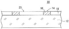
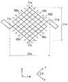
도 1 및 도 2에 도시된 바와 같이, 제 1 실시형태에 따른 도전성 필름 (10) 은 투명 기판 (12) (도 2 참조) 과 투명 기판 (12) 의 일 주면 상에 형성된 도전부 (14) 를 갖는다. 도전부 (14) 는, 금속의 세선 (이하, 금속 세선 (16) 으로 칭함) 과 개구부 (18) 를 포함하는 메시 패턴 (20) 을 갖는다. 예를 들어, 금속 세선 (16) 은 금 (Au), 은 (Ag) 또는 구리 (Cu) 를 포함한다.As shown in FIG. 1 and FIG. 2, the
구체적으로, 도전부 (14) 에서, 복수의 제 1 금속 세선 (16a) 과 복수의 제 2 금속 세선 (16b) 이 교차하여 메시 패턴 (20) 을 형성하고, 제 1 금속 세선 (16a) 은 제 1 경사 방향 (도 1에 도시된 x 방향) 으로 연장되어 제 2 경사 방향 (도 1에 도시된 y 방향) 으로 피치 Ps로 배열되고, 그리고 제 2 금속 세선 (16b) 은 제 2 경사 방향으로 연장되어 제 1 경사 방향으로 피치 Ps로 배열된다. 이 경우, 제 1 경사 방향은 기준 방향 (예를 들어, 수평 방향) 에 대해 +30°~ +60°의 각도이고, 제 2 경사 방향은 기준 방향에 대해 -30°~ -60°의 각도이다. 결과적으로, 메시 패턴 (20) 에서, 1개의 개구부 (18) 와 1개의 개구부 (18) 를 둘러싸는 4개의 금속 세선 (16) 의 조합인, 각각의 메시 형상 (22) 은 꼭지각들이 60°~ 120°인 마름모꼴 형상이다.Specifically, in the
도전성 필름 (10) 은 도 3에 도시된 표시 디바이스 (30) 의 전자파 실드 필름, 터치 패널의 도전성 필름 등으로서 사용될 수 있다. 이러한 표시 디바이스 (30) 의 예들은 액정 디스플레이, 플라즈마 디스플레이, 유기 EL 디스플레이, 및 무기 EL 디스플레이를 포함한다.The
피치 Ps (이하, 세선 피치 Ps 라고도 칭함) 는, 100 ~ 400㎛ 의 범위 내에서 선택될 수도 있다. 금속 세선 (16) 의 선폭은 30㎛ 이하일 수도 있다. 도전성 필름 (10) 이 전자파 실드 필름으로서 사용되는 경우, 금속 세선 (16) 의 선폭은 1 ~ 20㎛ 가 바람직하고, 1 ~ 9㎛ 가 보다 바람직하고, 2 ~ 7㎛ 가 더욱 바람직하다. 도전성 필름 (10) 이 도전성 터치 패널 필름으로 사용되는 경우, 금속 세선 (16) 의 선폭은 0.1 ~ 15㎛ 가 바람직하고, 1 ~ 9㎛ 가 보다 바람직하고, 2 ~ 7㎛ 가 더욱 바람직하다.The pitch Ps (hereinafter also referred to as thin wire pitch Ps) may be selected within a range of 100 to 400 μm. The line width of the
마름모꼴 메시 형상 (22) 은 4개의 꼭지각들 중 2개의 좁은 꼭지각을 가지며, 각각의 좁은 각의 반은 30°~ 44°이다. 즉, 가상선 (24) 이 개구부 (18) 에서 수평 방향으로 연장되어 메시 패턴 (20) 내의 복수의 교차점들을 접속시키는 경우, 가상선 (24) 과 제 1 금속 세선 (16a) 사이의 각도 θ (경사 각도 θ) 는 30°~ 44°이다.The
도 3에서 부분적으로 생략하여 도시된 바와 같이, 복수의 화소들 (32) 이 표시 디바이스 (30) 에서 매트릭스로 배열된다. 1개의 화소 (32) 는 수평 방향으로 배열되는 3개의 서브화소들 (적색 서브화소 (32r), 녹색 서브화소 (32g) 및 청색 서브화소 (32b)) 을 포함한다. 각각의 서브화소는 수직 방향으로 연장되는 직사각형 형상을 갖는다. 화소들 (32) 의 수평 방향으로의 배열 피치 (수평 화소 피치 Ph) 와 화소들 (32) 의 수직 방향으로의 배열 피치 (수직 화소 피치 Pv) 는 거의 서로 동일하다. 즉, 1개의 화소 (32) 및 1개의 화소 (32) 를 둘러싸는 블랙 매트릭스의 조합 (음영 영역 (34)) 은 사각형 형상을 형성한다. 각 화소 (32) 는 종횡비가 1이 아니고, 수평 (횡) 길이가 수직 (종) 길이보다 더 길다.As shown partially omitted in FIG. 3, a plurality of
도 4를 참조하여, 메시 형상 (22) 의 마름모꼴의 크기를 후술한다. 마름모꼴에서, 수직 방향으로 연장되는 하나의 대각선이 길이 Lvp 를 갖고 수평 방향으로 연장되는 다른 대각선이 길이 Lhp 를 가지는 경우, 마름모꼴의 크기, 즉, 종횡비 (Lvp/Lhp) 는 0.57<Lvp/Lhp<1.74 의 조건을 만족한다.With reference to FIG. 4, the size of the lozenge of the
화소들 (32) 이, 터치 패널 (50) 이 부착되는 표시 디바이스 (30) (도 3 참조) 에서 수평 방향으로 배열되는 경우, 마름모꼴의 종횡비 (Lvp/Lhp) 는 0.57<Lvp/Lhp<1.00 또는 1.00<Lvp/Lhp<1.74 의 조건을 만족하고, 보다 바람직하게 0.62<Lvp/Lhp<0.81 또는 1.23<Lvp/Lhp<1.61 의 조건을 만족한다.When the
도 5에 도시된 바와 같이, 이와 같은 화소 배열을 갖는 표시 디바이스 (30) 의 표시 패널 상에 도전성 필름 (10) 이 배치되는 경우, 금속 세선 (16) 은, 표시 디바이스 (30) 에서의 화소 (32) 의 수평 배열 방향 (m 방향) 에 대해 소정의 경사 각도 θ를 형성한다. 도 1에 도시된 바와 같이, 가상선 (24) 이 개구부 (18) 에서 수평 방향으로 연장되고 메시 패턴 (20) 의 복수의 교차점을 접속하며, 그리고 가상선 (24) 과 제 1 금속 세선 (16a) 사이의 각도 θ는 30°~ 60°이고, 바람직하게는 30°~ 44°이다. 따라서, 도 4에 도시된 바와 같이, 금속 세선 (16) 은, 표시 디바이스 (30) 에서의 화소 (32) 의 수평 배열 방향 (m 방향) 에 대해 30°~ 60°로 기울어지고, 바람직하게는 30°~ 44°로 기울어진다. 도전성 필름 (10) 의 세선 피치 Ps는 표시 디바이스 (30) 에서의 1개의 화소 (32) 의 대각선 길이 La1 (또는 수직 방향으로 배열되는 2개의 인접하는 화소들 (32) 의 대각선 길이 La2) 와 거의 동일하거나 또는 근접한다. 또한, 도전성 필름 (10) 에서의 금속 세선 (16) 의 배열 방향은 표시 디바이스 (30) 에서의 1개의 화소 (32) 의 대각선 (또는 수직 방향으로 배열되는 2개의 인접하는 화소들 (32) 의 대각선) 의 방향과 거의 동일하거나 또는 근접한다. 결과적으로, 화소들 (32) 과 금속 세선들 (16) 사이의 배열 주기 차이가 감소되어, 모아레 발생을 억제할 수 있다.As shown in FIG. 5, when the
예를 들어, 도전성 필름 (10) 이 전자파 실드 필름으로서 사용되는 경우, 도전성 필름 (10) 은 표시 디바이스 (30) 의 표시 패널 상에 배치된다. 이 경우, 상술한 바와 같이, 화소들 (32) 과 금속 세선들 (16) 사이의 배열 주기 차이가 감소되어, 모아레 발생을 억제할 수 있다. 또한, 메시 패턴 (20) 내의 금속 세선들 (16) 이 100 ~ 400㎛ 의 피치 Ps 및 30㎛ 이하의 선폭을 갖기 때문에, 전자파 실드 필름은 높은 전자파 실드 특성과 높은 광 투과성의 양자를 발휘할 수 있다.For example, when the
이와 같은 투영형 정전용량방식 (projected capacitive) 터치 패널을 갖는 표시 디바이스는 도 6 ~ 도 16을 참조하여 후술한다.A display device having such a projected capacitive touch panel will be described later with reference to FIGS. 6 to 16.
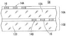
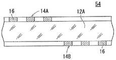
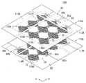
터치 패널 (50) 은 센서 본체 (52) 및 집적 회로와 같은 제어 회로 (미도시) 를 갖는다. 도 6, 도 7 및 도 8a에 도시된 바와 같이, 센서 본체 (52) 는 후술될 제 1 도전성 필름 (10A) 와 제 2 도전성 필름 (10B) 를 적층함으로써 제조된 도전성 필름 적층체 (54) 를 포함하고, 그 위의 보호층 (56) (도 8a에는 미도시) 을 더 포함한다. 도전성 필름 적층체 (54) 및 보호층 (56) 은 액정 디스플레이와 같은 표시 디바이스 (30) 의 표시 패널 (58) 상에 배치될 수 있다. 상부로부터 볼 때, 센서 본체 (52) 는 표시 패널 (58) 의 표시 화면 (58a) 에 대응하는 감지 영역 (60) 및 표시 패널 (58) 의 주변에 대응하는 단자 배선 영역 (62) (이른바 프레임) 를 갖는다.The
도 7 및 도 9에 도시된 바와 같이, 터치 패널 (50) 에서, 제 1 도전성 필름 (10A) 은 제 1 투명 기판 (12A) (도 8a 참조) 의 일 주면 상에 형성된 제 1 도전부 (14A) 를 갖는다. 제 1 도전부 (14A) 는 2 이상의 제 1 도전 패턴들 (64A) (메시 패턴들) 및 제 1 보조 패턴들 (66A) 을 포함한다. 제 1 도전 패턴들 (64A) 은 수평 방향 (m 방향) 으로 연장되고, 제 3 방향과 직교하는 수직 방향 (n 방향) 으로 배열되고, 각각이 다수의 격자들을 포함하며, 그리고 금속 세선들 (16) 로 구성된다. 제 1 보조 패턴들 (66A) 은 제 1 도전 패턴들 (64A) 주변에 배열되고 금속 세선들 (16) 로 구성된다.As shown in FIG. 7 and FIG. 9, in the
제 1 도전 패턴 (64A) 은 2 이상의 소격자들 (70) 을 갖는다. 도 7 및 도 9의 예에서, 제 1 도전 패턴 (64A) 은 2 이상의 제 1 대격자들 (68A) (제 1 감지부들) 을 포함한다. 제 1 대격자들 (68A) 은 수평 방향으로 직렬로 접속되고, 그리고 각각은 2 이상의 소격자들 (70) 의 조합을 포함한다. 상기 제 1 보조 패턴 (66A) 은 제 1 대격자 (68A) 의 측변 주위에 형성되고, 제 1 대격자 (68A) 와 접속되지 않는다. 예를 들어, m 방향은 후술될 투영형 정전용량방식 터치 패널 (50) 또는 그 터치 패널 (50) 이 설치된 표시 패널 (58) 의 수평 방향 또는 수직 방향에 대응한다 (도 6 참조).The first
제 1 도전 패턴 (64A) 은 제 1 대격자들 (68A) 을 이용한 예에 한정되지 않는다. 예를 들어, 제 1 도전 패턴 (64A) 은, 다수의 소격자들 (70) 이 배열되어 띠형상의 메시 패턴을 형성하고, 복수의 띠형상의 메시 패턴들이 평행하게 배열되고 절연부에 의해 서로 절연되는, 것일 수도 있다. 예를 들어, 2 이상의 띠형상의 제 1 도전 패턴들 (64A) 은 각각 단자로부터 m 방향으로 연장될 수도 있고 그리고 n 방향으로 배열될 수도 있다.The first
이 예에서, 소격자 (70) 는 도면에서 가장 작은 마름모꼴로 도시되고, 그리고 상기 메시 형상 (22) (도 1 및 도 4 참조) 과 동일하거나 또는 유사한 형상을 갖는다. 도 10에 도시된 바와 같이, 소격자 (70) 에서, (제 1 측변 ~ 제 4 측변 (70a ~ 70d) 의) 적어도 1개의 측변과 제 1 방향 (m 방향) 사이의 각도 θ는 30°~ 60°이다. m 방향이 터치 패널 (50) 을 갖는 표시 디바이스 (30) (도 5 참조) 의 화소 배열 방향과 같은 경우, 각도 θ는 30°~ 44°또는 46°~ 60°, 보다 바람직하게 32°~ 39°또는 51°~ 58°이다.In this example, the
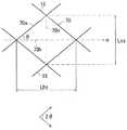
제 1 대격자 (68A) 의 크기는 도 11을 참조하여 후술된다. 제 1 대격자 (68A) 의 4개의 측변들 (제 1 측변 ~ 제 4 측변 (69a ~ 69d)) 중에서, 제 1 측변 (69a) 과 제 2 측변 (69b) 은 수평 방향 (m 방향) 으로 서로 인접하여 배열되고, 그리고 제 1 측변 (69a) 와 제 2 측변 (69b) 의 교차부는 제 1 코너 (71a) 에 대응한다. 마찬가지로, (제 1 측변 (69a) 과 대면하는) 제 3 측변 (69c) 과 (제 2 측변 (69b) 과 대면하는) 제 4 측변 (69d) 은 수평 방향으로 서로 인접하여 배열되고, 그리고 제 3 측변 (69c) 과 제 4 측변 (69d) 의 교차부는 제 2 코너 (71b) 에 대응한다.The size of the first
또한, 제 1 대격자 (68A) 의 4개의 측변 (제 1 측변 ~ 제 4 측변 (69a ~ 69d)) 중에서, 제 1 측변 (69a) 및 제 4 측변 (69d) 은 수직 방향 (n 방향) 으로 서로 인접하여 배열되고, 제 1 측변 (69a) 의 연장선과 제 4 측변 (69d) 의 교차점은 제 3 코너 (71c) 에 대응한다. 마찬가지로, 제 2 측변 (69b) 과 제 3 측변 (69c) 은 수직 방향으로 서로 인접하여 배열되고, 제 2 측변 (69b) 과 제 3 측변 (69c) 의 연장선의 교차점은 제 4 코너 (71d) 에 대응한다.Further, among the four side edges (first side edge to fourth side edges 69a to 69d) of the first
제 1 대격자 (68A) 의 제 2 방향 길이는 수직 방향의 제 1 코너 (71a) 와 제 2 코너 (71b) 사이의 거리 Lva 에 대응하고, 그리고 제 1 대격자 (68A) 의 제 1 방향 길이는 수평 방향의 제 3 코너 (71c) 와 제 4 코너 (71d) 사이의 거리 Lha 에 대응한다.The second direction length of the first
이 경우, 제 1 대격자 (68A) 의 크기, 즉, 제 1 대격자 (68A) 의 종횡비 (Lva/Lha) 는 0.57<Lva/Lha<1.74 의 조건을 만족한다.In this case, the size of the first
수평 방향 (m 방향) 이 터치 패널 (50) 을 갖는 표시 디바이스 (30) (도 6 참조) 의 화소 배열 방향과 같은 경우, 제 1 대격자 (68A) 의 종횡비 (Lva/Lha) 는 0.57<Lva/Lha<1.00 또는 1.00<Lva/Lha<1.74 의 조건을 만족하고, 보다 바람직하게 0.62<Lva/Lha<0.81 또는 1.23<Lva/Lha<1.61 의 조건을 만족한다.When the horizontal direction (m direction) is the same as the pixel array direction of the display device 30 (see FIG. 6) having the
또한 소격자 (70) 는 유사한 조건을 만족한다. 도 12에 도시된 바와 같이, 수직 방향으로 연장되는 하나의 대각선 (70v) 이 길이 Lvs 를 갖고, 수평 방향으로 연장되는 다른 대각선 (70h) 이 길이 Lhs 를 가지는 경우, 소격자 (70) 의 크기, 즉, 소격자 (70) 의 종횡비 (Lvs/Lhs) 는 0.57<Lvs/Lhs<1.74 의 조건을 만족한다.The
수평 방향이 터치 패널 (50) 을 갖는 표시 디바이스 (30) (도 6 참조) 의 화소 배열 방향과 동일한 경우, 또한 소격자 (70) 의 종횡비 (Lvs/Lhs) 는 0.57<Lvs/Lhs<1.00 또는 1.00<Lvs/Lhs<1.74 의 조건을 만족하고, 보다 바람직하게 0.62<Lvs/Lhs<0.81 또는 1.23<Lvs/Lhs<1.61 의 조건을 만족한다.When the horizontal direction is the same as the pixel arrangement direction of the display device 30 (see FIG. 6) having the
상술한 바와 같이, 소격자 (70) (즉, 금속 세선 (16)) 의 선폭은 30㎛ 이하 일 수도 있다. 소격자 (70) 의 측변 길이는 100 ~ 400㎛ 범위 내에서 선택될 수도 있다. 부수적으로, 제 1 대격자 (68A) 에서, 제 1 경사 방향 (x 방향) 은 제 1 측변 (69a) (및 제 3 측변 (69c)) 에 평행하고, 제 2 경사 방향 (y 방향) 은 제 2 측변 (69b) (및 제 4 측변 (69d)) 에 평행하다.As described above, the line width of the small lattice 70 (that is, the fine metal wire 16) may be 30 μm or less. The side length of the
예를 들어, 도 9에 도시된 바와 같이, 제 1 도전 패턴들 (64A) 에서 제 1 대격자들 (68A) 을 사용하는 경우, 금속 세선 (16) 으로 구성되는 제 1 접속부 (72A) 는 제 1 대격자들 (68A) 사이에서 형성되고, 제 1 대격자들 (68A) 의 각각의 인접하는 2개는 제 1 접속부 (72A) 에 의해 전기적으로 접속된다. 제 1 접속부 (72A) 는 중격자 (74) 를 포함하고, 중격자 (74) 의 크기는 제 2 경사 방향 (y 방향) 으로 배열된 n개의 소격자들 (70) (여기서 n은 1보다 큰 실수) 의 총 크기에 대응한다. 제 1 결제부 (first absent portion) (76A) (소격자 (70) 로부터 일 측변을 제거함으로써 제공된 부분) 는, 제 1 경사 방향을 따라 연장되는 제 1 대격자 (68A) 의 측변과 중격자 (74) 사이에 형성된다. 도 9의 예에서, 중격자 (74) 의 크기는 제 2 경사 방향으로 배열된 3개의 소격자들 (70) 의 총 크기에 대응한다.For example, as shown in FIG. 9, when using the first
전기적으로 절연된 제 1 절연부 (78A) 가 인접하는 제 1 도전 패턴들 (64A) 사이에 배치된다.An electrically insulated first insulating
제 1 보조 패턴 (66A) 은, (제 1 경사 방향에 평행하는 제 1 대격자 (68A) 의 측변을 따라 배열된) 제 2 경사 방향에 평행하는 축 방향을 갖는 복수의 제 1 보조선 (80A), (제 2 경사 방향에 평행하는 제 1 대격자 (68A) 의 측변을 따라 배열된) 제 1 경사 방향에 평행하는 축 방향을 갖는 복수의 제 1 보조선 (80A), 및 서로 대면하여 배열되는 2개의 제 1 L-형상 패턴들 (82A) 을 포함한다. 제 1 L-형상 패턴들 (82A) 의 각각은 2개의 제 1 보조선들 (80A) 을 제 1 절연부 (78A) 에서 L 형상으로 조합함으로써 형성된다.The first
제 1 대격자 (68A) 의 측변 길이는 3 ~ 10 mm 인 것이 바람직하고, 4 ~ 6 mm 인 것이 보다 바람직하다. 예를 들어, 터치 패널에서 제 1 도전성 필름 (10A) 을 사용하는 경우 측변 길이가 하한 미만일 때, 제 1 대격자들 (68A) 은 검출 공정에서 보다 낮은 정전 용량을 나타내고, 터치 패널은 검출 불량을 일으키기 쉽다. 한편, 측변 길이가 상한을 초과하는 경우, 위치 검출 정확도는 저하될 수도 있다. 동일한 이유 때문에, 제 1 대격자들 (68A) 에서 각각의 소격자 (70) 의 측변 길이는 상술한 바와 같이 100 ~ 400㎛ 인 것이 바람직하고, 150 ~ 300㎛ 인 것이 더욱 바람직하고, 210 ~ 250㎛ 인 것이 가장 바람직하다. 소격자 (70) 의 측변 길이가 이 범위 내인 경우, 제 1 도전성 필름 (10A) 은 높은 투명성을 가지고, 이로써 우수한 시인성을 갖는 표시 디바이스의 정면에서 적합하게 사용될 수 있다.It is preferable that it is 3-10 mm, and, as for the side length of the 1st
도 7에 도시된 바와 같이, 상기 구조를 갖는 제 1 도전성 필름 (10A) 에서, 각각의 제 1 도전 패턴 (64A) 의 일 단부에서, 제 1 접속부 (72A) 는 제 1 대격자 (68A) 의 개방단 상에 형성되지 않는다. 제 1 도전 패턴 (64A) 의 다른 단부에서, 제 1 대격자 (68A) 의 단부는 제 1 결선부 (first wire connection) (84a) 에 의해 금속 세선 (16) 으로 구성되는 제 1 단자 배선 패턴 (86a) 에 전기적으로 접속된다.As shown in FIG. 7, in the first
즉, 도 6 및 도 7에 도시된 바와 같이, 터치 패널 (50) 에서 사용되는 제 1 도전성 필름 (10A) 에서, 다수의 상기 제 1 도전 패턴들 (64A) 이 감지 영역 (60) 에 배열되고, 복수의 제 1 단자 배선 패턴들 (86a) 이 단자 배선 영역 (62) 에서 제 1 결선부들 (84a) 로부터 연장된다.That is, as shown in FIGS. 6 and 7, in the first
도 6의 예에서, 제 1 도전성 필름 (10A) 및 감지 영역 (60) 각각은 상부로부터 볼 때 직사각형 형상을 갖는다. 단자 배선 영역 (62) 에서, 복수의 제 1 단자들 (88a) 은 제 1 도전성 필름 (10A) 의 일 장변측의 주연부의 길이 방향으로 세로 중심에 배열된다. 제 1 결선부 (84a) 는 감지 영역 (60) 의 일 장변 (제 1 도전성 필름 (10A) 의 일 장변에 가장 가까운 장변) 을 따라 n 방향으로 직선으로 배열된다. 제 1 단자 배선 패턴 (86a) 은 각각의 제 1 결선부 (84a) 로부터 제 1 도전성 필름 (10A) 의 일 장변의 중심까지 연장되고, 상응하는 제 1 단자 (88a) 에 전기적으로 접속된다.In the example of FIG. 6, each of the first
한편, 도 7, 도 8a 및 도 13에 도시된 바와 같이, 제 2 도전성 필름 (10B) 은 제 2 투명 기판 (12B) (도 8a 참조) 의 일 주면 상에 형성된 제 2 도전부 (14B) 를 갖는다. 제 2 도전부 (14B) 는 2 이상의 제 2 도전 패턴들 (64B) 및 제 2 보조 패턴들 (66B) 을 포함한다. 제 2 도전 패턴들 (64B) 은 수직 방향 (n 방향) 으로 연장되고, 수평 방향 (m 방향) 으로 배열되며, 각각이 다수의 격자들을 포함하며, 그리고 금속 세선들 (16) 로 구성된다. 제 2 보조 패턴 (66B) 은 제 2 도전 패턴들 (64B) 주위에 배열되고 금속 세선들 (16) 로 구성된다.On the other hand, as shown in Figs. 7, 8A, and 13, the second
제 2 도전 패턴 (64B) 은 2 이상의 소격자들 (70) 을 갖는다. 도 7 및 도 13의 예에서, 제 2 도전 패턴 (64B) 은 2 이상의 제 2 대격자들 (68B) (제 2 감지부들) 을 포함한다. 제 2 대격자들 (68B) 은 수직 방향 (n 방향) 으로 직렬로 접속되고, 각각이 2 이상의 소격자들 (70) 의 조합을 포함한다. 상기 제 2 보조 패턴 (66B) 은 제 2 대격자 (68B) 의 측변 주위에 형성되고 제 2 대격자 (68B) 에 접속되지 않는다.The second
또한 제 2 도전 패턴 (64B) 은 제 2 대격자들 (68B) 을 사용한 예에 한정되지 않는다. 예를 들어, 제 2 도전 패턴 (64B) 은, 다수의 소격자들 (70) 이 배열되어 띠 형상의 메시 패턴을 형성하고, 그리고 복수의 띠 형상의 메시 패턴들이 평행하게 배열되고 절연부에 의해 서로 절연되는 것일 수도 있다. 예를 들어, 2 이상의 띠 형상의 제 2 도전 패턴들 (64B) 은 각각 단자로부터 n 방향으로 연장될 수도 있고 그리고 m 방향으로 배열될 수도 있다.In addition, the 2nd
제 2 대격자 (68B) 의 크기는 도 14를 참조하여 후술된다. 제 2 대격자 (68B) 의 4개의 측변들 (제 5 측변 ~ 제 8 측변 (69e ~ 69h)) 중에서, 제 5 측변 (69e) 과 제 6 측변 (69f) 은 수평 방향으로 서로 인접하여 배열되고, 그리고 제 5 측변 (69e) 과 제 6 측변 (69f) 의 연장선의 교차점은 제 5 코너 (71e) 에 대응한다. 마찬가지로, (제 5 측변 (69e) 과 대면하는) 제 7 측변 (69g) 과 (제 6 측변 (69f) 과 대면하는) 제 8 측변 (69h) 은 수평 방향으로 서로 인접하여 배열되고, 그리고 제 7 측변 (69g) 과 제 8 측변 (69h) 의 연장선의 교차점은 제 6 코너 (71f) 에 대응한다.The size of the second
또한, 제 2 대격자 (68B) 의 4개의 측변들 (제 5 측변 ~ 제 8 측변 (69e ~ 69h)) 중에서, 제 5 측변 (69e) 과 제 8 측변 (69h) 은 수직 방향으로 서로 인접하여 배열되고, 그리고 제 5 측변 (69e) 과 제 8 측변 (69h) 의 교차점은 제 7 코너 (71g) 에 대응한다. 마찬가지로, 제 6 측변 (69f) 과 제 7 측변 (69g) 은 수직 방향으로 서로 인접하여 배열되고, 그리고 제 6 측변 (69f) 과 제 7 측변 (69g) 의 교차점은 제 8 코너 (71h) 에 대응한다.Further, among the four side edges (the fifth side edge to the eighth side edges 69e to 69h) of the second
제 2 대격자 (68B) 의 제 2 방향 길이는 수직 방향 (n 방향) 의 제 5 코너 (71e) 와 제 6 코너 (71f) 사이의 거리 Lvb 에 대응하고, 제 2 대격자 (68B) 의 제 1 방향 길이는 수평 방향 (m 방향) 의 제 7 코너 (71g) 와 제 8 코너 (71h) 사이의 거리 Lhb 에 대응한다.The second directional length of the second
이 경우, 제 2 대격자 (68B) 의 크기, 즉, 제 2 대격자 (68B) 의 종횡비 (Lvb/Lhb) 는 0.57<Lvb/Lhb<1.74 의 조건을 만족한다.In this case, the size of the second
수평 방향 (m 방향) 이 터치 패널 (50) 을 갖는 표시 디바이스 (30) (도 6 참조) 의 화소 배열 방향과 동일한 경우, 제 2 대격자 (68B) 의 종횡비 (Lvb/Lhb) 는 0.57<Lvb/Lhb<1.00 또는 1.00<Lvb/Lhb<1.74 의 조건을 만족하고, 보다 바람직하게 0.62<Lvb/Lhb<0.81 또는 1.23<Lvb/Lhb<1.61 의 조건을 만족한다.When the horizontal direction (m direction) is the same as the pixel array direction of the display device 30 (see FIG. 6) having the
부수적으로, 제 2 대격자 (68B) 에서, 제 1 경사 방향 (x 방향) 은 제 5 측변 (69e) (및 제 7 측변 (69g)) 에 평행하고, 그리고 제 2 경사 방향 (y 방향) 은 제 6 측변 (69f) (및 제 8 측변 (69h)) 에 평행하다.Incidentally, in the second
제 2 도전 패턴들 (64B) 에서 제 2 대격자 (68B) 를 사용한 경우, 예를 들어, 도 13에 도시된 바와 같이, 금속 세선들 (16) 로 구성되는 제 2 접속부들 (72B) 이 제 2 대격자들 (68B) 사이에 형성되고, 그리고 제 2 대격자들 (68B) 의 각각의 인접하는 2개는 제 2 접속부 (72B) 에 의해 전기적으로 접속된다. 제 2 접속부 (72B) 는 중격자 (74) 를 포함하고, 그리고 중격자 (74) 의 크기는 제 1 경사 방향 (x 방향) 으로 배열된 n개의 소격자들 (70) (여기서 n은 1보다 큰 실수) 의 총 크기에 대응한다. 제 2 결제부 (76B) (소격자 (70) 로부터 일 측변을 제거함으로써 제공된 부분) 는, 제 2 경사 방향을 따라 연장되는 제 2 대격자 (68A) 의 측변과 중격자 (74) 사이에 형성된다.When the second
전기적으로 절연된 제 2 절연부 (78B) 는 인접하는 제 2 도전 패턴들 (64B) 사이에 배치된다.The electrically insulated
제 2 보조 패턴 (66B) 은, (제 1 경사 방향에 평행하는 제 2 대격자 (68B) 의 측변에 따라 배열되는) 제 2 경사 방향에 평행하는 축 방향을 갖는 복수의 제 2 보조선들 (80B), (제 2 경사 방향에 평행하는 제 2 대격자 (68B) 의 측변을 따라 배열된) 제 1 경사 방향에 평행하는 축 방향을 갖는 복수의 제 2 보조선들 (80B), 및 서로 대면하여 배열되는 2개의 제 2 L-형상 패턴들 (82B) 을 포함한다. 제 2 L-형상 패턴들 (82B) 의 각각은 2개의 제 2 보조선들 (80B) 을 제 2 절연부 (78B) 에서 L 형상으로 조합함으로써 형성된다.The second
도 6 및 도 7에 도시된 바와 같이, 상기 구조를 갖는 제 2 도전성 필름 (10B) 에서, 예를 들어, 각각의 교호하는 (홀수 번째의) 제 2 도전 패턴 (64B) 의 일 단부 및 각각의 짝수 번째의 제 2 도전 패턴 (64B) 의 다른 단부의 각각에서, 제 2 접속부 (72B) 는 제 2 대격자 (68B) 의 개방단 상에 형성되지 않는다. 각각의 홀수 번째의 제 2 도전 패턴 (64B) 의 다른 단부 및 각각의 짝수 번째의 제 2 도전 패턴 (64B) 의 일 단부의 각각에서, 제 2 대격자 (68B) 의 단부가 제 2 결선부 (84b) 에 의해 금속 세선들 (16) 로 구성되는 제 2 단자 배선 패턴 (86b) 에 전기적으로 접속된다.6 and 7, in the second
즉, 도 7에 도시된 바와 같이, 터치 패널 (50) 에서 사용되는 제 2 도전성 필름 (10B) 에 있어서, 다수의 상기 제 2 도전 패턴들 (64B) 이 감지 영역 (60) 에 배열되고, 그리고 복수의 제 2 단자 배선 패턴들 (86b) 이 단자 배선 영역 (62) 에서 제 2 결선부들 (84B) 로부터 연장된다.That is, as shown in FIG. 7, in the second
도 6에 도시된 바와 같이, 단자 배선 영역 (62) 에 있어서, 복수의 제 2 단자들 (88B) 이 제 2 도전성 필름 (10B) 의 일 장변측의 주연부의 길이 방향으로 세로 중심에 배열된다. 예를 들어, 홀수 번째의 제 2 결선부 (84B) 는 감지 영역 (60) 의 일 단변 (제 2 도전성 필름 (10B) 의 일 단변에 가장 가까운 단변) 을 따라 m 방향으로 직선으로 배열되고, 그리고 짝수 번째의 제 2 결선부 (84B) 는 감지 영역 (60) 의 다른 단변 (제 2 도전성 필름 (10B) 의 다른 단변에 가장 가까운 단변) 을 따라 m 방향으로 직선으로 배열된다.As shown in FIG. 6, in the
예를 들어, 각각의 홀수 번째의 제 2 도전 패턴 (64B) 이 대응하는 홀수 번째의 제 2 결선부 (84b) 에 접속되고, 그리고 각각의 짝수 번째의 제 2 도전 패턴 (64B) 이 대응하는 짝수 번째의 제 2 결선부 (84b) 에 접속된다. 제 2 단자 배선 패턴들 (86b) 은 홀수 번째 및 짝수 번째의 제 2 결선부 (84b) 로부터 제 2 도전성 필름 (10B) 의 일 장변의 중심까지 인출되고, 각각 상응하는 제 2 단자들 (88b) 에 전기적으로 접속된다.For example, each odd second
제 1 단자 배선 패턴들 (86a) 은 상기 제 2 단자 배선 패턴들 (86b) 과 동일한 방식으로 배열될 수도 있고, 그리고 제 2 단자 배선 패턴들 (86b) 은 상기 제 1 단자 배선 패턴들 (86a) 과 동일한 방식으로 배열될 수도 있다.The first
제 2 대격자들 (68B) 의 측변 길이는 제 1 대격자 (68A) 와 마찬가지로 3 ~ 10 mm 인 것이 바람직하고, 4 ~ 6 mm 인 것이 보다 바람직하다. 측변 길이가 하한 미만인 경우, 제 2 대격자 (68B) 는 저하된 정전 용량을 나타내어 검출 프로세스에서 검출 불량을 일으킬 가능성이 있다. 다른 한편, 측변 길이가 상한을 초과하는 경우, 위치 검출 정확도가 저하될 수도 있다. 동일한 이유로, 제 2 대격자들 (68B) 에서 각 소격자의 측변 길이는 100 ~ 400㎛ 인 것이 바람직하고, 150 ~ 300㎛ 인 것이 더욱 바람직하고, 210 ~ 250㎛ 인 것이 가장 바람직하다. 소격자 (70) 의 측변 길이가 이 범위 내인 경우, 제 2 도전성 필름 (10B) 은 높은 투명성을 가지고, 이로써 표시 디바이스 (30) 의 표시 패널 (58) 상에 우수한 시인성을 가지고 적합하게 사용될 수 있다.The side length of the second
제 1 보조 패턴들 (66A) (제 1 보조선들 (80A)) 및 제 2 보조 패턴들 (66B) (제 2 보조선들 (80B)) 의 각각의 선폭은 30㎛ 이하이고, 그리고 제 1 도전 패턴들 (64A) 및 제 2 도전 패턴들 (64B) 의 선폭과 동일하거나 또는 상이할 수도 있다. 제 1 도전 패턴들 (64A), 제 2 도전 패턴들 (64B), 제 1 보조 패턴들 (66A) 및 제 2 보조 패턴들 (66B) 이 동일한 선폭을 갖는 것이 바람직하다.The line width of each of the first
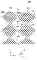
예를 들어, 도 15에 도시된 바와 같이, 제 1 도전성 필름 (10A) 이 제 2 도전성 필름 (10B) 상에 적층되어 도전성 필름 적층체 (54) 를 형성할 때, 제 1 도전 패턴들 (64A) 과 제 2 도전 패턴들 (64B) 이 교차된다. 구체적으로, 제 1 도전 패턴들 (64A) 의 제 1 접속부들 (72A) 과 제 2 도전 패턴들 (64B) 의 제 2 접속부들 (72B) 이 제 1 투명 기판 (12A) (도 8a 참조) 을 사이에 개재하여 서로 대면하여 배열되고, 그리고 또한 제 1 도전부 (14A) 의 제 1 절연부 (78A) 와 제 2 도전부 (14B) 의 제 2 절연부 (78B) 가 제 1 투명 기판 (12A) 을 사이에 개재하여 서로 대면하여 배열된다.For example, as shown in FIG. 15, when the first
도 15에 도시된 바와 같이, 도전성 필름 적층체 (54) 가 상부로부터 관찰되는 경우, 제 1 도전성 필름 (10A) 의 제 1 대격자들 (68A) 사이의 공간들은 제 2 도전성 필름 (10B) 의 제 2 대격자들 (68B) 에 의해 충전된다. 이 경우, 제 1 보조 패턴들 (66A) 과 제 2 보조 패턴들 (66B) 이 서로 중첩하여, 제 1 대격자들 (68A) 과 제 2 대격자들 (68B) 사이에 조합 패턴들 (90) 을 형성한다. 도 16에 도시된 바와 같이, 조합 패턴 (90) 에서, 제 1 보조선 (80A) 의 제 1 축 (92A) 은 제 2 보조선 (80B) 의 제 2 축 (92B) 에 대응하고, 제 1 보조선 (80A) 은 제 2 보조선 (80B) 과 중첩하지 않으며, 그리고 제 1 보조선 (80A) 의 단부는 제 2 보조선 (80B) 의 단부에 대응하며, 이로써 소격자 (70) (메시 형상) 의 일 측변이 형성된다. 따라서, 조합 패턴 (90) 은 2 이상의 소격자들 (70) (메시 형상) 의 조합을 포함한다. 결과적으로, 도 15에 도시된 바와 같이, 도전성 필름 적층체 (54) 가 상부로부터 관찰되는 경우, 전체 표면은 다수의 소격자들 (70) (메시 형상) 로 커버된다.As shown in FIG. 15, when the
도전성 필름 적층체 (54) 가 표시 디바이스 (30) 의 표시 패널 (58) 상에 배치되는 경우, 예를 들어, 도 5에 도시된 바와 같이, 제 1 경사 방향 (x 방향) 으로 연장되고 제 2 경사 방향 (y 방향) 으로 세선 피치 Ps 로 배열되는 복수의 금속 세선들 (16), 및 제 2 경사 방향으로 연장되고 제 1 경사 방향으로 세선 피치 Ps 로 배열되는 복수의 금속 세선들 (16) 이 교차되어 메시 패턴 (20) 을 형성한다. 각각의 금속 세선 (16) 은 표시 디바이스 (30) 에서의 화소들 (32) 의 수평 배열 방향 (m 방향) 에 대해 소정의 경사 각도 θ를 형성한다. 다수의 소격자들 (70) 에서 각각의 금속 세선 (16) 은 표시 디바이스 (30) 에서의 화소들 (32) 의 수평 배열 방향 (m 방향) 에 대해 30°~ 60°의 각도이고, 바람직하게 30°~ 44°의 각도이다. 도전성 필름 적층체 (54) 의 세선 피치 Ps 는 표시 디바이스 (30) 에서 1개의 화소 (32) 의 대각선 길이 La1 (또는 수직 방향으로 배열되는 2개의 인접하는 화소들 (32) 의 대각선 길이 La2) 과 대략 동일하거나 또는 근접하고, 그리고 도전성 필름 적층체 (54) 에서의 금속 세선들 (16) 의 배열 방향은 표시 디바이스 (30) 에서 1개의 화소 (32) 의 대각선 (또는 수직 방향으로 배열되는 2개의 인접하는 화소들 (32) 의 대각선) 의 방향과 대략 동일하거나 또는 근접한다. 결과적으로, 화소들 (32) 과 금속 세선들 (16) 사이의 배열 주기 차이는 감소되어, 모아레 발생을 억제할 수 있다. 또한, 도전성 필름 적층체 (54) 에서 제 1 대격자 (68A) 의 종횡비가 제 2 대격자 (68B) 의 종횡비와 크게 상이한 경우라도, 모아레 발생이 효과적으로 억제될 수 있다. 즉, 도전성 필름 적층체 (54) 가 개선된 수율로 획득될 수 있다.When the
도전성 필름 적층체 (54) 가 터치 패널에서 사용되는 경우, 보호층 (56) 이 제 1 도전성 필름 (10A) 상에 형성되고, 그리고 제 1 도전성 필름 (10A) 에서 제 1 도전 패턴들 (64A) 로부터 연장되는 제 1 단자 배선 패턴들 (86a) 과 제 2 도전성 필름 (10B) 에서 제 2 도전 패턴들 (64B) 로부터 연장되는 제 2 단자 배선 패턴들 (86b) 이 스캔 제어 회로 등에 접속된다.When the
터치 위치 검출을 위해 자기 용량 테크놀로지 또는 상호 용량 테크놀로지가 바람직하게 사용될 수 있다. 자기 용량 테크놀로지에서, 터치 위치 검출을 위한 전압 신호가 제 1 도전 패턴들 (64A) 에 순차적으로 공급되고, 또한 터치 위치 검출을 위한 전압 신호가 제 2 도전 패턴들 (64B) 에 순차적으로 공급된다. 손가락이 보호층 (56) 의 상부 표면과 접촉하거나 또는 근접하게 되는 경우, 터치 위치에서의 제 1 도전 패턴 (64A) 및 제 2 도전 패턴 (64B) 과 GND (그라운드) 사이의 용량이 증가되어, 이로써 이 제 1 도전 패턴 (64A) 및 이 제 2 도전 패턴 (64B) 으로부터의 신호들이 다른 도전 패턴들로부터의 신호들과 상이한 파형을 갖는다. 즉, 터치 위치가 제 1 도전 패턴 (64A) 및 제 2 도전 패턴 (64B) 으로부터 전송된 신호에 기초하여 제어 회로에 의해 계산된다. 다른 한편, 상호 용량 테크놀로지에서는, 예를 들어, 터치 위치 검출을 위한 전압 신호가 제 1 도전 패턴들 (64A) 에 순차적으로 공급되고, 그리고 제 2 도전 패턴들 (64B) 이 순차적으로 감지 (전송된 신호 검출) 를 실시한다. 손가락이 보호층 (56) 의 상부 표면과 접촉하거나 또는 근접하게 되는 경우, 손가락의 병렬 부유 용량 (parallel stray capacitance) 이 터치 위치에서의 제 1 도전 패턴 (64A) 과 제 2 도전 패턴 (64B) 사이의 기생 용량에 더해져서, 이로써 이 제 2 도전 패턴 (64B) 으로부터의 신호가 다른 제 2 도전 패턴들 (64B) 로부터의 신호들과 상이한 파형을 갖는다. 즉, 전압 신호가 공급되는 제 1 도전 패턴 (64A) 의 순서와 제 2 도전 패턴 (64B) 으로부터 전송된 신호에 기초하여 제어 회로에 의해 터치 위치가 계산된다. 2개의 손가락이 보호층 (56) 의 상부 표면에 동시에 접촉하거나 또는 근접하게 되는 경우라도, 터치 위치들은 자기 용량 테크놀로지 또는 상호 용량 테크놀로지를 이용하여 검출될 수 있다. 투영형 정전용량방식 테크놀로지에서 사용되는 종래의 관련 검출 회로들은 미국 특허 제 4,582,955호, 제 4,686,332호, 미국 특허 제 4,733,222호, 제 5,374,787호, 제 5,543,588호, 및 제 7,030,860호, 미국 특허 출원 공개공보 제 2004/0155871호 등에 기재되어 있다.Magneto-capacitance technology or mutual capacitance technology can be preferably used for touch position detection. In the capacitance technology, a voltage signal for touch position detection is sequentially supplied to the first
제 2 실시형태는 도 17 ~ 도 21을 참조하여 후술된다. 도 17에 도시된 바와 같이, 제 2 실시형태에 따른 도전성 필름 적층체 (104) 는, 제 1 실시형태에 따른 도전성 필름 적층체 (54) 와 동일한 방식으로 제 1 도전성 필름 (110A) 과 제 2 도전성 필름 (110B) 을 적층함으로써 제조된다. 도전성 필름 적층체 (104) 는, 예를 들어, 도 6에 도시된 표시 디바이스 (30) 상의 터치 패널 (50) 의 센서 본체 (52) 에서 사용될 수 있다. 도전성 필름 (110) (제 1 도전성 필름 (110A) 및 제 2 도전성 필름 (110B)) 은, 도 3에 도시된 표시 디바이스 (30) 의 전자파 실드 필름, 도전성 터치 패널 필름 등으로서 사용될 수 있다.The second embodiment will be described later with reference to FIGS. 17 to 21. As shown in FIG. 17, the
도 17, 도 18a 및 도 19에 도시된 바와 같이, 제 1 도전성 필름 (110A) 은 제 1 투명 기판 (112A) (도 18a 참조) 및 제 1 투명 기판 (112A) 의 일 주면 상에 형성된 제 1 도전부 (114A) 를 갖는다. 제 1 도전부 (114A) 는 2 이상의 제 1 도전 패턴들 (116A) (메시 패턴들) 및 제 1 보조 패턴들 (120A) 을 포함한다. 제 1 도전 패턴들 (116A) 은 수평 방향 (m 방향) 으로 연장되고, 수평 방향에 직교하는 수직 방향 (n 방향) 으로 배열되고, 각각이 다수의 격자들을 포함하며, 그리고 금속 세선들 (16) 로 구성된다. 제 1 보조 패턴들 (120A) 은 제 1 도전 패턴들 (116A) 주위에 배열되고 금속 세선들 (16) 로 구성된다. 예를 들어, 수평 방향 (m 방향) 은 투영형 정전용량식 터치 패널 (50) 또는 터치 패널 (50) 이 설치된 표시 패널 (58) 의 수평 방향 또는 수직 방향에 대응한다. 또한, 이 예에서, 소격자 (70) 는 도면에서 가장 작은 마름모꼴로 도시되고, 제 1 실시형태의 상기 메시 형상 (22) (도 1 및 도 4 참조) 과 같은 형상 또는 유사한 형상을 갖는다.As shown in FIGS. 17, 18A, and 19, the first
제 1 실시형태는 물론, 제 2 실시형태에서, 도 12에 도시된 바와 같이, 소격자 (70) 의 종횡비 (Lvs/Lhs) 는 0.57<Lvs/Lhs<1.74 의 조건을 만족한다. 수평 방향이 터치 패널 (50) 을 갖는 표시 디바이스 (30) (도 6 참조) 의 화소 배열 방향과 동일한 경우에는, 소격자 (70) 의 종횡비 (Lvs/Lhs) 는 0.57<Lvs/Lhs<1.00 또는 1.00<Lvs/Lhs<1.74 의 조건을 만족하고, 보다 바람직하게 0.62<Lvs/Lhs<0.81 또는 1.23<Lvs/Lhs<1.61 의 조건을 만족한다. 상술한 바와 같이, 소격자 (70) (즉, 금속 세선 (16)) 의 선폭은 30㎛ 이하일 수도 있다. 소격자 (70) 의 측변 길이는 100 ~ 400㎛ 의 범위 내에서 선택될 수도 있다.In the second embodiment as well as the first embodiment, as shown in FIG. 12, the aspect ratio Lvs / Lhs of the
제 1 도전 패턴 (116A) 은, 2 이상의 제 1 대격자들 (118A) (제 1 감지부들) 을 포함한다. 제 1 대격자들 (118A) 은 수평 방향 (m 방향) 으로 직렬로 접속되고, 그리고 각각이 2 이상의 소격자들 (70) 의 조합을 포함한다. 상기 제 1 보조 패턴 (120A) 은 제 1 대격자 (118A) 의 측변 주위에 형성되고, 제 1 대격자 (118A) 에 접속되지 않는다.The first
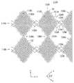
제 1 대격자 (118A) 는 실질적으로 마름모꼴 형상을 가지며, 이것은 사변들에 1 이상의 단차들 (122) 을 포함하는 제 1 계단 패턴들 (124A) 을 갖는다. 단차 (122) 의 높이는 소격자 (70) 의 높이의 정수배와 동일하다. 도 19의 예에서, 제 1 대격자 (118A) 의 사변 상에, 2개의 단차들 (122) 이 수직으로 연장되는 코너로부터 수평으로 연장되는 코너를 향하는 방향으로 제 3 및 제 7 소격자들 (70) 상에 형성되고, 단차들 (122) 의 높이는 1개의 소격자 (70) 의 높이와 동일하다. 제 1 계단 패턴 (124A) 은, 소격자들 (70) 의 열이 제 1 대격자 (118A) 에서 수직으로 연장되는 코너로부터 수평으로 연장되는 코너로의 방향으로 단차 (122) 를 가지고 감소되는 것이다.The first
상술한 바와 같이, 제 1 대격자 (118A) 는 실질적으로 마름모꼴 형상을 갖는다. 보다 구체적으로, 제 1 대격자 (118A) 는 주판알 형상을 가지며, 이것은 수평으로 연장되는 코너에서 여러개의 소격자들 (70) 을 제거함으로써 제공된다. 즉, r개의 소격자들 (70) (여기서 r은 1보다 큰 정수) 가 수직 방향으로 배열되어 2개의 수평으로 연장되는 코너들의 각각에 제 1 상부 베이스 (126A) 를 형성하고, 그리고 1개의 소격자 (70) 가 위치하여 수직으로 연장되는 코너들의 각각에 꼭지각을 형성한다. 도 19에서, 4개의 소격자들 (70) 이 수직 방향으로 배열되어 제 1 대격자 (118A) 의 2개의 수평으로 연장되는 코너들의 각각에 제 1 상부 베이스 (126A) 를 형성한다.As described above, the first
이 경우, 제 1 대격자 (118A) 에 내포되는 가장 큰 마름모꼴 (즉, 수평으로 연장되는 코너 상의 2개의 제 1 상부 베이스들 (126A) 사이에 형성되는 가장 큰 마름모꼴) 의 종횡비가 편의상 제 1 대격자 (118A) 의 종횡비 (Lva/Lha) 로 여겨지는 경우, 종횡비 (Lva/Lha) 는 0.57<Lva/Lha<1.74 의 조건을 만족한다.In this case, the aspect ratio of the largest lozenge (i.e., the largest lozenge formed between two first
수평 방향 (m 방향) 이 터치 패널 (50) 을 갖는 표시 디바이스 (30) (도 6 참조) 의 화소 배열 방향과 동일한 경우, 제 1 대격자 (118A) 의 종횡비 (Lva/Lha) 는 0.57<Lva/Lha<1.00 또는 1.00<Lva/Lha<1.74 의 조건을 만족하고, 보다 바람직하게 0.62<Lva/Lha<0.81 또는 1.23<Lva/Lha<1.61 의 조건을 만족한다.When the horizontal direction (m direction) is the same as the pixel arrangement direction of the display device 30 (see FIG. 6) having the
제 1 결제부 (128A) (소격자 (70) 로부터 일 측변을 제거함으로써 제공된 부분) 가 수평으로 연장되는 코너 상의 2개의 제 1 상부 기재 (126A) 와 제 1 경사 방향 (x 방향) 에 따라 연장되는 제 1 대격자 (118A) 의 사변 사이에 형성된다.Two first
도 19에 도시된 바와 같이, 금속 세선들 (16) 로 구성되는 제 1 접속부들 (132A) 이 제 1 대격자들 (118A) 사이에 형성되고, 그리고 제 1 대격자들 (118A) 의 각각의 인접하는 2개가 제 1 접속부 (132A) 에 의해 전기적으로 접속된다. 제 1 접속부 (132A) 는 제 1 중격자들 (134A 및 136A) 을 포함한다. 제 1 중격자 (134A) 의 크기는 제 2 경사 방향 (y 방향) 으로 배열되는 n개의 소격자들 (70) (여기서 n은 1보다 큰 정수) 의 총 크기에 대응한다. 제 1 중격자 (136A) 의 크기는 p × q 개의 소격자들 (70) 의 총 크기에 대응한다 (여기서 p 및 q는 각각 1보다 큰 정수). 즉, 제 1 중격자 (136A) 는, p개의 소격자들 (70) 이 제 2 경사 방향으로 배열되고 q개의 소격자들 (70) 이 제 1 경사 방향으로 배열되는 것이다. 도 19의 예에서, n 은 7이고, 이로써 제 1 중격자 (134A) 의 크기는 제 2 경사 방향으로 배열되는 7개의 소격자들 (70) 의 총 크기에 대응한다. 도 19의 예에서, p (제 2 경사 방향에서의 수) 는 3 이고, q (제 1 경사 방향에서의 수) 는 5이며, 이로써 제 1 중격자 (136A) 의 크기는 15개의 소격자들 (70) 의 총 크기에 대응한다.As shown in FIG. 19, first connecting
제 1 결제부 (128A) (소격자 (70) 로부터 일 측변을 제거함으로써 제공된 부분) 가 제 1 중격자 (136A) 와 제 1 대격자 (118A) 사이에 형성된다.A
제 1 비접속부 (138A) 가 수평 방향으로 배열되는 인접하는 제 1 도전 패턴들 (116A) 사이에 배치되고, 그리고 제 1 대격자들 (118A) 의 각각의 인접하는 2개가 제 1 비접속부 (138A) 에 의해 서로 절연된다.The first
상기 제 1 보조 패턴 (120A) 은 제 1 도전부 (114A) 에서 제 1 대격자 (118A) 의 측변 주위에 형성되고, 그리고 제 1 대격자 (118A) 에 접속되지 않는다. 제 1 보조 패턴 (120A) 은 제 1 경사 방향에 평행한 제 1 대격자 (118A) 의 사변 상의 제 1 계단 패턴 (124A) 을 따라 배열된 (제 2 경사 방향에 평행한 축 방향을 갖는) 복수의 제 1 보조선들 (130A), 제 2 경사 방향에 평행한 제 1 대격자 (118A) 의 사변 상의 제 1 계단 패턴 (124A) 을 따라 배열된 (제 1 경사 방향에 평행한 축 방향을 갖는) 복수의 제 1 보조선들 (130A), 및 2개의 제 1 보조선들 (130A) 을 L 형상으로 조합함으로써 형성된 제 1 L-형상 패턴 (131A) 을 포함한다.The first
각각의 제 1 보조선 (130A) 의 축 방향의 길이는, 소격자 (70) 의 내측 측변 길이의 1/2 이다. 제 1 보조선 (130A) 은 제 1 대격자 (118A) 로부터 소정 거리에 배치된다. 소정 거리는 이 예에서 소격자 (70) 의 내측 측변 길이의 1/2과 동일하다.The length of the 1st
제 1 L-형상 패턴 (131A) 은, 제 1 경사 방향에 평행한 축 방향을 갖는 제 1 보조선 (130A) 과 제 2 경사 방향에 평행한 축 방향을 갖는 제 1 보조선 (130A) 을 조합함으로써 제 1 계단 패턴 (124A) 의 단차 (122) 부근에 형성된다. 제 1 L-형상 패턴 (131A) 은 단차 (122) 의 코너에 대면하거나 또는 제 1 대격자들 (118A) 사이의 제 1 비접속부 (138A) 에 배치된다. 도 19에 도시된 바와 같이, 제 1 비접속부 (138A) 에서, 2개의 제 1 보조선들 (130A) 이 1개의 제 1 대격자 (118A) 의 수직으로 연장되는 코너의 부근에 배치되고, 그리고 2개의 제 1 보조선들 (130A) 이 인접하는 제 1 대격자 (118A) 의 수직으로 연장되는 코너의 부근에 배치되며, 이로써 2개의 제 1 L-형상 패턴들 (131A) 이 수평 방향으로 서로 대면하여 배열된다.The first L-shaped
제 1 대격자들 (118A) 에서 각각의 소격자 (70) 의 측변 길이는 50㎛ 이상인 것이 바람직하고, 100 ~ 400㎛ 인 것이 보다 바람직하고, 150 ~ 300㎛ 인 것이 더욱 바람직하고, 210 ~ 250㎛ 인 것이 가장 바람직하다. 소격자 (70) 의 측변 길이가 이 범위 내인 경우, 제 1 도전성 필름 (110A) 은 높은 투명성을 가지며, 이로써 우수한 시인성을 가지고 표시 디바이스의 전면에서 적합하게 사용될 수 있다.The side length of each
도 17에 도시된 바와 같이, 상기 구조를 갖는 제 1 도전성 필름 (110A) 에 있어서, 각각의 제 1 도전 패턴 (116A) 의 일 단부에서는, 제 1 접속부 (132A) 가 제 1 대격자 (118A) 의 개방단 상에 형성되지 않는다. 제 1 도전 패턴 (116A) 의 다른 단부에서는, 제 1 대격자 (118A) 의 단부가 제 1 결선부 (84a) 에 의해 금속 세선 (16) 으로 구성되는 제 1 단자 배선 패턴 (86a) 에 접속된다.As shown in FIG. 17, in the first
다른 한편, 도 17, 도 18a 및 도 20에 도시된 바와 같이, 제 2 도전성 필름 (110B) 은 제 2 투명 기판 (112B) (도 18a 참조) 의 일 주면 상에 형성된 제 2 도전부 (114B) 를 갖는다. 제 2 도전부 (114B) 는 2 이상의 제 2 도전 패턴들 (116B) (메시 패턴들) 및 제 2 보조 패턴 (120B) 를 갖는다. 제 2 도전 패턴들 (116B) 은 수직 방향 (n 방향) 으로 연장되고, 수평 방향 (m 방향) 으로 배열되며, 각각이 다수의 격자들을 포함하며, 그리고 금속 세선들 (16) 로 구성된다. 제 2 보조 패턴들 (120B) 은 제 2 도전 패턴들 (116B) 의 주위에 배열되고 금속 세선들 (16) 로 구성된다.On the other hand, as shown in FIGS. 17, 18A, and 20, the second
제 2 도전 패턴 (116B) 은 2 이상의 제 2 대격자들 (제 2 감지부들) (118B) 을 포함한다. 제 2 대격자들은 수직 방향 (n 방향) 으로 직렬로 접속되고, 그리고 각각이 2 이상의 소격자들 (70) 의 조합을 포함한다. 상기 제 2 보조 패턴 (120B) 은 제 2 대격자 (118B) 의 측벽 주위에 형성되고, 제 2 대격자 (118B) 에 접속되지 않는다.The second
제 2 대격자 (118B) 는 실질적으로 마름모꼴 형상을 가지며, 이것은 사변들 상에 1 이상의 단차들 (122) 을 포함하는 제 2 계단 패턴들 (124B) 을 갖는다. 단차 (122) 의 높이는 소격자 (70) 의 높이의 정수배와 동일하다. 도 20의 예에서, 제 2 대격자 (118B) 의 사변 상에서, 2개의 단차들 (122) 이 4개의 소격자들 (70) 의 간격으로 형성되며, 그리고 단차들 (122) 의 높이는 1개의 소격자 (70) 의 높이와 동일하다. 제 2 계단 패턴 (124B) 은, 소격자들 (70) 의 열이 제 2 대격자 (118B) 에 있어서 수평으로 연장되는 코너로부터 수직으로 연장되는 코너로의 방향으로 단차 (122) 를 가지고 증가되는 것이다.The second
상술한 바와 같이, 제 2 대격자 (118B) 는 실질적으로 마름모꼴 형상을 갖는다. 보다 구체적으로, 제 2 대격자 (118B) 는 주판알 형상을 가지며, 이것은 수직으로 연장되는 코너에서 여러개의 소격자들 (70) 을 제거함으로써 제공된다. 즉, r개의 소격자들 (70) (여기서 r은 1보다 큰 정수) 이 수평 방향으로 배열되어 2개의 수직으로 연장되는 코너들의 각각에 제 2 상부 베이스 (126B) 를 형성하고, 그리고 1개의 소격자 (70) 가 위치하여 수평으로 연장되는 코너들의 각각에 꼭지각을 형성한다. 도 20에서, 4개의 소격자들 (70) 이 수평 방향으로 배열되어 제 2 대격자 (118B) 의 2개의 수직으로 연장되는 코너들의 각각에 제 2 상부 베이스 (126B) 를 형성한다.As described above, the second
이 경우, 제 2 대격자 (118B) 에 내포되는 가장 큰 마름모꼴 (즉, 수평으로 연장되는 코너들 사이에 형성되는 가장 큰 마름모꼴) 의 종횡비가 편의상 제 2 대격자 (118B) 의 종횡비 (Lva/Lha) 로 여겨지는 경우, 종횡비 (Lva/Lha) 는 0.57<Lva/Lha<1.74 의 조건을 만족한다.In this case, the aspect ratio of the largest lozenge (ie, the largest lozenge formed between the horizontally extending corners) contained in the second
수평 방향 (m 방향) 이 터치 패널 (50) 을 갖는 표시 디바이스 (30) (도 6 참조) 의 화소 배열 방향과 동일한 경우, 제 2 대격자 (118B) 의 종횡비 (Lva/Lha) 는 0.57<Lva/Lha<1.00 또는 1.00<Lva/Lha<1.74 의 조건을 만족하고, 보다 바람직하게 0.62<Lva/Lha<0.81 또는 1.23<Lva/Lha<1.61 의 조건을 만족한다.When the horizontal direction (m direction) is the same as the pixel array direction of the display device 30 (see FIG. 6) having the
제 2 결제부 (128B) (소격자 (70) 로부터 일 측변을 제거함으로써 제공된 부분) 가 수직으로 연장되는 코너 상의 2개의 제 2 상부 기재 (126B) 와 제 2 경사 방향에 따라 연장되는 제 2 대격자 (118B) 의 사변 사이에 형성된다.Two second
도 20에 도시된 바와 같이, 금속 세선들 (16) 로 구성되는 제 2 접속부들 (132B) 이 제 2 대격자들 (118B) 사이에 형성되고, 그리고 수직으로 배열되는 제 2 대격자들 (118B) 의 각각의 인접하는 2개가 제 2 접속부 (132B) 에 의해 접속된다. 제 2 접속부 (132B) 는 제 2 중격자들 (134B 및 136B) 을 포함한다. 제 2 중격자 (134B) 의 크기는 제 1 경사 방향으로 배열되는 n개의 소격자들 (70) (여기서 n은 1보다 큰 정수) 의 총 크기에 대응한다. 제 2 중격자 (136B) 의 크기는 p × q 개의 소격자들 (70) 의 총 크기에 대응한다 (여기서 p 및 q는 각각 1보다 큰 정수). 즉, 제 2 중격자 (136B) 는, p개의 소격자들 (70) 이 제 1 경사 방향으로 배열되고 q개의 소격자들 (70) 이 제 2 경사 방향으로 배열되는 것이다. 도 20의 예에서, n 은 7이고, 이로써 제 2 중격자 (134B) 의 크기는 제 1 경사 방향으로 배열되는 7개의 소격자들 (70) 의 총 크기에 대응한다. 도 20의 예에서, p (제 1 경사 방향에서의 수) 는 3 이고, q (제 2 경사 방향에서의 수) 는 5이며, 이로써 제 2 중격자 (136B) 의 크기는 15개의 소격자들 (70) 의 총 크기에 대응한다.As shown in FIG. 20, second connecting
제 2 결제부 (128B) (소격자 (70) 로부터 일 측변을 제거함으로써 제공된 부분) 가 제 2 중격자 (136B) 와 제 2 대격자 (118B) 사이에 형성된다.The
제 2 비접속부 (138B) 가 수평 방향으로 배열되는 인접하는 제 2 도전 패턴들 (116B) 사이에 배치되고, 그리고 제 2 대격자들 (118B) 의 각각의 인접하는 2개가 제 2 비접속부 (138B) 에 의해 서로 절연된다.The second
상기 언급된 제 2 보조 패턴 (120B) 은 제 2 도전부 (114BA) 에서 제 2 대격자 (118B) 의 측변 주위에 형성되고, 그리고 제 2 대격자 (118B) 에 접속되지 않는다. 제 2 보조 패턴 (120B) 은 제 2 경사 방향에 평행한 제 2 대격자 (118B) 의 사변 상의 제 1 계단 패턴 (124B) 을 따라 배열된 (제 1 경사 방향에 평행한 축 방향을 갖는) 복수의 제 2 보조선들 (130B), 제 1 경사 방향에 평행한 제 2 대격자 (118B) 의 사변 상의 제 1 계단 패턴 (124B) 을 따라 배열된 (제 2 경사 방향에 평행한 축 방향을 갖는) 복수의 제 2 보조선들 (130B), 및 2개의 제 2 보조선들 (130B) 을 L 형상으로 조합함으로써 형성된 제 2 L-형상 패턴 (131B) 을 포함한다.The above-mentioned second
각각의 제 2 보조선 (130B) 의 축 방향 길이는, 제 1 보조선 (130A) 과 동일한 방식으로, 소격자 (70) 의 내측 측변 길이의 1/2 이다. 제 2 보조선 (130B) 은 제 2 대격자 (118B) 로부터 소정의 거리에 배치된다. 또한 소정의 거리는, 상술된 제 1 보조선 (130A) 과 동일한 방식으로, 소격자 (70) 의 내측 측변 길이의 1/2 과 동일하다.The axial length of each 2nd
제 2 L-형상 패턴 (131B) 은, 제 2 경사 방향에 평행한 축 방향을 갖는 제 2 보조선 (130B) 과 제 2 경사 방향에 평행한 축 방향을 갖는 제 2 보조선 (130B) 을 조합함으로써 제 1 계단 패턴 (124B) 의 단차 (122) 부근에 형성된다. 제 2 L-형상 패턴 (131B) 은 단차 (122) 의 코너에 대면하거나 또는 제 2 대격자들 (118B) 사이의 제 2 비접속부 (138B) 에 배치된다. 도 20에 도시된 바와 같이, 제 2 비접속부 (138B) 에서, 2개의 제 2 보조선들 (130B) 이 1개의 제 2 대격자 (118B) 의 수평으로 연장되는 코너의 부근에 배치되고, 그리고 2개의 제 2 보조선들 (130B) 이 인접하는 제 2 대격자 (118B) 의 수평으로 연장되는 코너의 부근에 배치되며, 이로써 2개의 제 2 L-형상 패턴들 (131B) 이 수직 방향으로 서로 대면하여 배열된다.The second L-shaped
제 2 대격자들 (118B) 에서 각각의 소격자 (70) 의 측변 길이는 50㎛ 이상인 것이 바람직하고, 100 ~ 400㎛ 인 것이 보다 바람직하고, 150 ~ 300㎛ 인 것이 더욱 바람직하고, 210 ~ 250㎛ 인 것이 가장 바람직하다. 소격자 (70) 의 측변 길이가 이 범위 내인 경우, 제 2 도전성 필름 (110B) 은 높은 투명성을 가지고, 이로써 우수한 시인성을 가지고 표시 디바이스의 전면에서 적합하게 사용될 수 있다.It is preferable that the side length of each
도 17에 도시된 바와 같이, 상기 구조를 갖는 제 2 도전성 필름 (110B) 에서, 예를 들어, 각각의 교호하는 홀수 번째의 제 2 도전 패턴 (116B) 의 일 단부에서 및 각각의 짝수 번째의 제 2 도전 패턴 (116B) 의 다른 단부에서, 제 2 접속부 (132B) 는 제 2 대격자 (118B) 의 개방단 상에 형성되지 않는다. 각각의 홀수 번째의 제 2 도전 패턴 (116B) 의 다른 단부에서 및 각각의 짝수 번째의 제 2 도전 패턴 (116B) 의 일 단부에서, 제 2 대격자 (118B) 의 단부가 제 2 결선부 (84b) 에 의해 금속 세선들 (16) 로 구성되는 제 2 단자 배선 패턴 (86b) 에 접속된다. 결과적으로, 제 2 도전성 필름 (110B) 은 제 1 실시형태와 동일한 방식으로 터치 패널 (50) 에서 사용된다.As shown in FIG. 17, in the second
제 1 도전 패턴들 (116A) (제 1 대격자들 (118A) 및 제 1 접속부들 (132A)) 및 제 2 도전 패턴들 (116B) (제 2 대격자들 (118B) 및 제 2 접속부들 (132B)) 각각의 선폭의 하한은 1㎛ 이상, 3㎛ 이상, 4㎛ 이상, 또는 5㎛ 이상이 바람직하고, 상한은 15㎛ 이하, 10㎛ 이하, 9㎛ 이하, 또는 8㎛ 이하가 바람직하다. 선폭이 하한 미만인 경우, 도전성 필름은 불충분한 도전성을 가지며, 이로써 필름을 사용하는 터치 패널은 불충분한 검출 감도를 갖는다. 다른 한편, 선폭이 상한을 초과하는 경우, 금속 세선 (16) 에 기인하여 모아레가 현저하게 발생되고, 그리고 그 필름을 사용한 터치 패널은 불량한 시인성을 갖는다. 선폭이 상기 범위 이내인 경우, 금속 세선 (16) 으로 구성되는 도전 패턴들의 모아레가 개선되고 시인성이 현저하게 개선된다. 적어도 제 1 투명 기판 (112A) 이 75 ~ 350㎛ 의 두께를 갖는 것이 바람직하다. 두께는 더욱 바람직하게 80 ~ 250㎛ 이고, 특히 바람직하게 100 ~ 200㎛ 이다.First
제 1 보조 패턴들 (120A) (제 1 보조선들 (130A)) 및 제 2 보조 패턴들 (120B) (제 2 보조선들 (130B)) 각각의 선폭의 하한은 1㎛ 이상, 3㎛ 이상, 4㎛ 이상, 또는 5㎛ 이상이 바람직하고, 상한은 15㎛ 이하, 10㎛ 이하, 9㎛ 이하, 또는 8㎛ 이하가 바람직하다. 이 선폭은 제 1 도전 패턴 (116A) 또는 제 2 도전 패턴 (116B) 의 선폭과 동일하거나 또는 상이할 수도 있다. 부수적으로, 제 1 도전 패턴 (116A), 제 2 도전 패턴 (116B), 제 1 보조 패턴 (120A) 및 제 2 보조 패턴 (120B) 이 동일한 선폭을 갖는 것이 바람직하다.The lower limit of the line width of each of the first
예를 들어, 도 21에 도시된 바와 같이, 제 1 도전성 필름 (110A) 이 제 2 도전성 필름 (110B) 상에 적층되어 도전성 필름 적층체 (104) 를 형성하는 경우, 제 1 도전 패턴들 (116A) 및 제 2 도전 패턴들 (116B) 이 교차된다. 구체적으로, 제 1 도전 패턴들 (116A) 의 제 1 접속부들 (132A) 과 제 2 도전 패턴들 (116B) 의 제 2 접속부들 (132B) 이 제 1 투명 기판 (112A) (도 18a 참조) 을 사이에 개재하여 서로 대면하여 배열되고, 그리고 또한 제 1 도전부 (114A) 의 제 1 비접속부들 (138A) 및 제 2 도전부 (114B) 의 제 2 비접속부들 (138B) 이 제 1 투명 기판 (112A) 을 사이에 개재하여 서로 대면하여 배열된다.For example, as shown in FIG. 21, when the first
도 21에 도시된 바와 같이, 도전성 필름 적층체 (104) 가 상부로부터 관찰되는 경우, 제 1 도전성 필름 (110A) 의 제 1 대격자들 (118A) 사이의 공간들이 제 2 도전성 필름 (110B) 의 제 2 대격자들 (118B) 로 충전된다.As shown in FIG. 21, when the
이 경우, 제 1 접속부들 (132A) 및 제 2 접속부들 (132B) 이 서로 중첩한다. 즉, 제 1 중격자들 (134A) 및 제 2 중격자들 (134B) 이 서로 중첩하고, 그리고 제 1 중격자들 (136A) 및 제 2 중격자들 (136B) 이 서로 중첩하여, 실질적으로 직사각형 형상을 갖는 조합 패턴들 (140) 을 형성한다. 조합 패턴 (140) 에서, 제 1 중격자 (134A) 및 제 2 중격자 (134B) 는 대각선 상에 배치된다. 도 19 및 도 20에 도시된 제 1 접속부 (132A) 및 제 2 접속부 (132B) 에 의해 형성되는 조합 패턴 (140) 에서, 7개의 소격자들 (70) 이 대각선 상에 배열되고, 그리고 4개의 소격자들 (70) 이 각각의 4개의 측변들 상에 배열된다. 즉, 조합 패턴 (140) 은 총 25개의 소격자들 (70) 을 포함한다. 조합 패턴 (140) 의 코너 상에, 제 2 대격자 (118B) 의 제 1 결제부 (128A) 에서 제거된 일 측변은 제 1 중격자 (134A) 에서의 소격자 (70) 의 일 측변에 의해 보상되고, 그리고 제 1 대격자 (118A) 의 제 1 결제부 (128A) 에서 제거된 일 측변은 제 2 중격자 (134B) 에서의 소격자 (70) 의 일 측변에 의해 보상된다.In this case, the first connecting
또한, 제 1 보조 패턴들 (120A) 및 제 2 보조 패턴들 (120B) 은 서로 중첩하여 제 1 대격자들 (118A) 및 제 2 대격자들 (118B) 사이에 조합 패턴들 (142) 을 형성한다. 도 6에 도시된 제 1 실시형태의 예와 동일한 방식으로, 조합 패턴 (142) 에서, 제 1 보조선 (130A) 의 제 1 축은 제 2 보조선 (130B) 의 제 2 축에 대응하고, 제 1 보조선 (130A) 은 제 2 보조선 (130B) 과 중첩하지 않으며, 그리고 제 1 보조선 (130A) 의 단부는 제 2 보조선 (130B) 의 단부에 대응하고, 이로써 소격자 (70) (메시 형상) 의 일 측변이 형성된다.Further, the first
따라서, 조합 패턴들 (140 및 142) 은 각각 2 이상의 소격자들 (70) (메시 형상들) 의 조합을 포함한다. 결과적으로, 도 21에 도시된 바와 같이, 도전성 필름 적층체 (104) 가 상부로부터 관찰되는 경우, 전체 표면이 다수의 소격자들 (70) (메시 형상) 로 커버된다. 제 2 실시형태의 기준 위치는, 소격자 (70) 의 일 측변이 제 1 보조선 (130A) 및 제 2 보조선 (130B) 에 의해 형성되는 그러한 위치이다.Thus, the
이 실시형태에서, 단차들 (122) 을 갖는 제 1 및 제 2 계단 패턴들 (124A 및 124B) 이 상기 방식으로 배열되고, 이로써 제 1 대격자들 (118A) 및 제 2 대격자들 (118B) 사이의 경계들이 더욱 잘 안 보이게 되어, 시인성이 향상된다.In this embodiment, the first and
도전성 필름 적층체 (104) 가 터치 패널에서 사용되는 경우, 보호층 (56) 이 제 1 도전성 필름 (110A) 상에 형성되고, 그리고 제 1 도전성 필름 (110A) 에서 제 1 도전 패턴들 (116A) 로부터 연장된 제 1 단자 배선 패턴들 (86a) 및 제 2 도전성 필름 (110B) 에서 제 2 도전 패턴들 (116B) 로부터 연장된 제 2 단자 배선 패턴 (86b) 이 스캔 제어 회로 등에 접속된다.When the
제 1 및 제 2 실시형태들의 상기 도전성 필름 적층체들 (54 및 104) 은 도 7, 도 8a, 도 17, 도 18a에 도시된 구조들을 갖는다. 예를 들어, 제 1 실시형태에서, 제 1 도전부 (14A) 가 제 1 투명 기판 (12A) 의 일 주면 상에 형성되고, 그리고 제 2 도전부 (14B) 가 제 2 투명 기판 (12B) 의 일 주면 상에 형성된다. 대안으로, 도 8b 및 도 18b에 도시된 바와 같이, 예를 들어, 제 1 실시형태에서, 제 1 도전부 (14A) 가 제 1 투명 기판 (12A) 의 일 주면 상에 형성될 수도 있고, 그리고 제 2 도전부 (14B) 가 제 1 투명 기판 (12A) 의 다른 주면 상에 형성될 수도 있다. 이 경우, 제 2 투명 기판 (12B) 이 사용되지 않고, 제 1 투명 기판 (12A) 이 제 2 도전부 (14B) 상에 적층되며, 그리고 제 1 도전부 (14A) 가 제 1 투명 기판 (12A) 상에 적층된다. 또한, 또 다른 층이 제 1 도전성 필름 (10A) 과 제 2 도전성 필름 (10B) 사이에 배치될 수도 있다. 제 1 도전 패턴들 (64A) 및 제 2 도전 패턴들 (64B) 은, 이들이 절연되는 한 서로 대면하여 배열될 수도 있다.The conductive film stacks 54 and 104 of the first and second embodiments have the structures shown in FIGS. 7, 8A, 17, and 18A. For example, in the first embodiment, the first
도 6에 도시된 바와 같이, 제 1 얼라인먼트 마크들 (94a) 및 제 2 얼라인먼트 마크들 (94b) 이 예를 들어 제 1 도전성 필름 (10A) 및 제 2 도전성 필름 (10B) 의 코너들 상에 형성되는 것이 바람직하다. 제 1 얼라인먼트 마크들 (94a) 및 제 2 얼라인먼트 마크들 (94b) 은, 필름들의 본딩 프로세스에서, 제 1 도전성 필름 (10A) 및 제 2 도전성 필름 (10B) 을 배치하기 위해 사용된다. 제 1 도전성 필름 (10A) 및 제 2 도전성 필름 (10B) 이 본딩되어 도전성 필름 적층체 (54) 를 획득하는 경우, 제 1 얼라인먼트 마크들 (94a) 및 제 2 얼라인먼트 마크들 (94b) 은 복합 얼라인먼트 마크들을 형성한다. 복합 얼라인먼트 마크들은, 도전성 필름 적층체 (54) 를 표시 패널 (58) 에 부착하는 프로세스에서 도전성 필름 적층체 (54) 를 배치하기 위해 사용될 수도 있다.As shown in FIG. 6, the first alignment marks 94a and the second alignment marks 94b are formed on corners of the first
상기 실시형태들에서 제 1 도전성 필름들 (10a 및 110A) 및 제 2 도전성 필름 (10B 및 110B) 이 투영형 정전용량방식 터치 패널 (50) 에 사용되지만, 이들은 표면형 정전용량방식 (surface capacitive) 터치 패널 또는 저항막식 (resistive) 터치 패널에 사용될 수 있다.In the above embodiments, the first
상기 실시형태들에서 도전성 필름들 (10 및 110) 이 전자파 실드 필름 또는 도전성 터치 패널 필름으로 사용되지만, 이들은 또한 표시 디바이스 (30) 의 표시 패널 (58) 을 위한 또 다른 광학 필름으로서 사용될 수 있다. 이 경우, 표시 패널 (58) 의 전체 표면이 도전성 필름의 메시 패턴으로 커버될 수도 있다. 표시 패널 (58) 의 전체 표면이 도전성 필름 (10 또는 110) 의 메시 패턴 (20) 으로 커버될 수도 있고, 그리고 표시 화면 (58a) 의 일부 (예컨대, 코너 또는 코너부) 만이 도전성 필름 (10 또는 110) 의 메시 패턴 (20) 으로 커버될 수도 있다.Although the
제 1 실시형태에 따른 도전성 필름 (10 또는 110) 의 제조 방법이 후술된다. 이 방법은 또한 제 2 실시형태에서 사용될 수 있다는 것이 이해되어야 한다.The manufacturing method of the
도전성 필름 (10) 은 다음과 같이 제조될 수도 있다. 예를 들어, 투명 기판 (12) 및 그 위의 감광성 할로겐화 은 함유 유제층을 갖는 감광성 재료가 노광 및 현상될 수도 있고, 이로써 금속 은부들 및 광 투과성부들이 노광 영역들 및 비노광 영역들에 각각 형성되어 메시 패턴 (20) 을 획득한다. 금속 은부들에는 물리 현상 처리 및/또는 도금 처리를 실시하여 그 위에 도전성 금속을 성막한다.The
대안으로, 도금 전처리 재료의 감광성 도금 베이스층이 제 1 투명 기판 (12A) 및 제 2 투명 기판 (12B) 상에 형성될 수도 있다. 결과물이 노광 및 현상되고, 그리고 도금 처리되어, 금속부들 및 광 투과성부들이 노광 영역들 및 비노광 영역들에 각각 형성되어, 제 1 도전 패턴들 (64A) 및 제 2 도전 패턴들 (64B) 을 형성할 수도 있다. 금속부들은 더욱 물리 현상 처리 및/또는 도금 처리되어, 그 위에 도전성 금속을 성막시킬 수도 있다.Alternatively, a photosensitive plating base layer of plating pretreatment material may be formed on the first
도금 전처리 재료를 이용하는 방법에 하기의 2가지 프로세스들이 바람직하게 사용될 수 있다. 그 프로세스들은 일본 공개특허공보 제 2003-213437호, 제 2006-64923호, 제 2006-58797호, 및 제 2006-135271호 등에 보다 구체적으로 개시되어 있다.The following two processes can preferably be used in the method using the plating pretreatment material. The processes are disclosed in more detail in Japanese Unexamined Patent Publication Nos. 2003-213437, 2006-64923, 2006-58797, 2006-135271, and the like.
(a) 투명 기판에, 도금 촉매 또는 그 전구체와 상호작용하는 관능기를 갖는 도금 베이스층을 도포하고, 그 층을 노광 및 현상하고, 그리고 현상된 층을 도금 처리하여, 도금 베이스 재료 상에 금속부를 형성하는 것을 포함하는 프로세스.(a) applying a plating base layer having a functional group interacting with a plating catalyst or a precursor thereof to a transparent substrate, exposing and developing the layer, and plating the developed layer to form a metal portion on the plating base material ≪ / RTI >
(b) 투명 기판에, 폴리머 및 금속 산화물을 포함하는 하부층과, 도금 촉매 또는 그 전구체와 상호작용하는 관능기를 갖는 도금 베이스층을 이 순서로 도포하고, 이 층들을 노광 및 현상하고, 그리고 현상된 층을 도금 처리하여, 도금 베이스 재료 상에 금속부를 형성하는 것을 포함하는 프로세스.(b) applying to the transparent substrate a lower layer comprising a polymer and a metal oxide, and a plating base layer having a functional group interacting with the plating catalyst or a precursor thereof in this order, exposing and developing these layers, And plating the layer to form a metal portion on the plating base material.
대안으로, 투명 기판 (12) 상에 배치된 구리 호일 상의 포토레지스트 막은 노광 및 현상되어 레지스트 패턴을 형성할 수도 있고, 그리고 레지스트 패턴으로부터 노출된 구리 호일은 에칭되어 메시 패턴 (20) 을 형성할 수도 있다.Alternatively, the photoresist film on the copper foil disposed on the
금속 미립자들을 포함하는 페이스트를 투명 기판 (12) 상에 인쇄할 수도 있고, 그리고 인쇄된 페이스트를 금속으로 도금하여 메시 패턴 (20) 을 형성할 수도 있다.A paste containing metal fine particles may be printed on the
메시 패턴 (20) 은 스크린 인쇄판 또는 그라비아 인쇄판을 이용함으로써 투명 기판 (12) 상에 인쇄될 수도 있다.The
메시 패턴 (20) 은 잉크젯 방법을 이용함으로써 투명 기판 (12) 상에 형성될 수도 있다.The
이 실시형태에 따른 도전성 필름 (10) 을 제조하기 위해 사진 감광성 할로겐화 은 재료를 이용하는 것을 포함하는, 특히 바람직한 방법이 주로 후술된다.Particularly preferred methods, including the use of photographic photosensitive silver halide materials, for producing the
이 실시형태의 도전성 필름 (10) 의 제조 방법은, 감광성 재료들과 현상 처리들이 상이한 하기의 3가지 프로세스들을 포함한다.The manufacturing method of the
(1) 물리적 현상 핵이 없는 감광성 흑백 할로겐화 은 재료를 화학적 또는 열적 현상으로 처리하여, 감광성 재료 상에 금속 은부들을 형성하는 것을 포함하는 프로세스.(1) A process comprising treating a photosensitive black-and-white halogenated silver-free material with a chemical or thermal development to form metal silver halide on the photosensitive material.
(2) 물리적 현상 핵을 포함하는 할로겐화 은 유제층을 갖는 감광성 흑백 할로겐화 은 재료를 용액 물리적 현상으로 처리하여, 감광성 재료 상에 금속 은부들을 형성하는 것을 포함하는 프로세스.(2) a process comprising treating a photosensitive black and white halogenated silver material having a silver halide emulsion layer containing a physical development nucleus with a solution physical phenomenon to form metal silver portions on the photosensitive material.
(3) 물리적 현상 핵이 없는 감광성 흑백 할로겐화 은 재료 및 물리적 현상 핵을 포함하는 비감광성 층을 갖는 수상 (image-receiving) 시트의 적층체를 확산 전사 현상 처리하여, 비감광성 수상 시트 상에 금속 은부들을 형성하는 것을 포함하는 프로세스.(3) Physical Development A layered product of an image-receiving sheet having a non-photosensitive layer containing a photosensitive black-and-white halogenated silver material and a physical developing nucleus, which is free of nuclei, is subjected to diffusion transfer development processing, ≪ / RTI >
(1) 의 프로세스에서, 일체형 흑백 현상 절차가 이용되어 감광성 재료 상에 광 투과성 도전성 필름과 같은 투과성 도전성 필름을 형성한다. 형성된 은은 높은 비표면적을 갖는 필라멘트를 포함하는 화학적으로 또는 열적으로 현상된 은이며, 이로써 하기의 도금 또는 물리적 현상 처리에서 높은 활성을 나타낸다.In the process of (1), an integral monochrome developing procedure is used to form a transparent conductive film such as a light-transmitting conductive film on a photosensitive material. The silver formed is a chemically or thermally developed silver comprising filaments having a high specific surface area, thereby exhibiting high activity in the following plating or physical development treatments.
(2) 의 프로세스에서, 할로겐화 은 입자들이 노광 영역 내의 물리적 현상 핵 주위에서 용융되고 물리적 현상 핵 상에 성막되어 감광성 재료 상에 광 투과성 도전성 필름과 같은 투과성 도전성 필름을 형성한다. 또한 이 프로세스에서도, 일체형 흑백 현상 절차가 이용된다. 할로겐화 은이 현상시 물리적 현상 핵 상에 성막되기 때문에 높은 활성이 달성될 수 있지만, 현상된 은은 작은 비표면을 가진 구형상을 갖는다.In the process of (2), the silver halide grains are melted around the physical developing nuclei in the exposure area and deposited on the physical developing nuclei to form a transparent conductive film such as a light-transmitting conductive film on the photosensitive material. Also in this process, an integral monochrome developing procedure is used. High activity can be achieved because silver halide is deposited on the physical developing nucleus during development, but developed silver has a spherical shape with a small specific surface.
(3) 의 프로세스에서, 할로겐화 은 입자들은 비노광 영역에서 용융되고, 수상 시트의 현상 핵 상에 확산 및 성막되어, 시트 상에 광 투과성 도전성 필름과 같은 투과성 도전성 필름을 형성한다. 이 프로세스에서, 소위 세퍼레이트 타입 절차가 이용되고, 수상 시트가 감광성 재료로부터 박리된다.In the process of (3), the silver halide grains are melted in the non-exposed region and diffused and deposited on the developing nuclei of the image-receiving sheet to form a transparent conductive film such as a light-transmitting conductive film on the sheet. In this process, a so-called separate type procedure is used, and the image receiving sheet is peeled from the photosensitive material.
네가티브 또는 반전 현상 처리가 프로세스들에서 이용될 수 있다. 확산 전사 현상에서는, 오토-포지티브 감광성 재료를 사용하여 네가티브 현상 처리가 실행될 수 있다.Negative or inverse developing processes can be used in processes. In the diffusion transfer phenomenon, a negative development process can be carried out using an auto-positive photosensitive material.
화학적 현상, 열적 현상, 용액 물리적 현상, 및 확산 전사 현상은 일반적으로 당업계에 알려진 의미를 가지며, Shin-ichi Kikuchi, "사진 화학 (Photographic Chemistry)", Kyoritsu Shuppan Co., Ltd., 1955 및 C. E. K. Mees, "The Theory of Photographic Processes, 4th ed.", Mcmillan, 1977 과 같은 일반 사진 화학 문서에 설명되어 있다. 액체 처리가 일반적으로 본 발명에서 이용되며, 또한 열적 현상 처리가 이용될 수 있다. 예를 들어, 일본 특허 공개공보 제 2004-184693호, 제 2004-334077호, 및 제 2005-010752로, 및 일본 특허 출원 제 2004-244080호 및 제 2004-085655호에 기재된 기술들이 본 발명에서 이용될 수 있다.Chemical phenomena, thermal phenomena, solution physical phenomena, and diffusion transcription phenomena generally have meanings known in the art and include Shin-ichi Kikuchi, “Photographic Chemistry”, Kyoritsu Shuppan Co., Ltd., 1955, and CEK. General photographic chemistry documents such as Mees, "The Theory of Photographic Processes, 4th ed.", Mcmillan, 1977. Liquid processing is generally used in the present invention, and thermal development processing can also be used. For example, the techniques described in Japanese Patent Laid-Open Nos. 2004-184693, 2004-334077, and 2005-010752, and Japanese Patent Applications 2004-244080 and 2004-085655 are used in the present invention. Can be.
이하, 이 실시형태의 도전성 필름 (10) 에서의 각 층의 구조가 상세히 설명된다.Hereinafter, the structure of each layer in the
[투명 기판 (12)][Transparent substrate 12]
투명 기판 (12) 은 플라스틱 필름, 플라스틱 판, 유리 판 등일 수도 있다.The
플라스틱 필름 및 플라스틱 판의 재료들의 예들은, 폴리에틸렌 테레프탈레이트 (PET) 및 폴리에틸렌 나프탈레이트 (PEN) 와 같은 폴리에스테르류, 그리고 트리아세틸 셀룰로오스 (TAC) 를 포함한다.Examples of materials of plastic film and plastic plate include polyesters such as polyethylene terephthalate (PET) and polyethylene naphthalate (PEN), and triacetyl cellulose (TAC).
투명 기판 (12) 은 바람직하게 융점이 약 290℃ 이하인 플라스틱 필름 또는 플라스틱 판이다. PET 가 광 투과성, 가공성 등의 관점에서 특히 바람직하다.The
[은염 유제층][Silver salt emulsion layer]
도전성 필름 (10) 의 금속 세선 (16) 으로 변환될 은염 유제층은 은염 및 바인더를 포함하고, 그리고 용매 및 염료와 같은 첨가제를 더 포함할 수도 있다.The silver salt emulsion layer to be converted into the
이 실시형태에서 사용되는 은염은 할로겐화 은과 같은 무기 은염 또는 아세트산 은과 같은 유기 은염일 수도 있다. 이 실시형태에서, 할로겐화 은은 그 우수한 광 감지 특성 때문에 바람직하다.The silver salt used in this embodiment may be an inorganic silver salt such as silver halide or an organic silver salt such as acetic acid silver. In this embodiment, silver halides are preferred because of their excellent light sensing properties.
은염 유제층의 도포 은 양 (도포된 은염의 은 밀도 양) 은 바람직하게 1 ~ 30 g/㎡, 보다 바람직하게 1 ~ 25 g/㎡, 더욱 바람직하게 5 ~ 20 g/㎡ 이다. 도포된 은 양이 이 범위 내인 경우, 형성된 도전성 필름 (10) 은 원하는 표면 저항을 나타낼 수 있다.The amount of silver applied (the silver density amount of the silver salt applied) of the silver salt emulsion layer is preferably 1 to 30 g / m 2, more preferably 1 to 25 g / m 2 and even more preferably 5 to 20 g / m 2. When the amount of silver applied is within this range, the formed
이 실시형태에서 사용되는 바인더들의 예들은 젤라틴, 폴리비닐 알코올 (PVA), 폴리비닐 피롤리돈 (PVP), 전분 등의 다당류, 셀룰로오스 및 그 유도체, 폴리에틸렌 산화물, 폴리비닐아민, 키토산, 폴리리신, 폴리아크릴산, 폴리알긴산, 폴리히알루론산, 및 카르복시셀룰로오스를 포함한다. 바인더들은 관능성기의 이온성에 의존하여 중성, 음이온성 또는 양이온성을 나타낸다.Examples of binders used in this embodiment include gelatin, polyvinyl alcohol (PVA), polyvinylpyrrolidone (PVP), polysaccharides such as starch, cellulose and its derivatives, polyethylene oxide, polyvinylamine, chitosan, polylysine, Polyacrylic acid, polyalginic acid, polyhyaluronic acid, and carboxycellulose. The binders are neutral, anionic or cationic depending on the ionic nature of the functional group.
이 실시형태에서, 은염 유제층에서의 바인더의 양은 특별히 한정되지 않으며, 충분한 분산성 및 접착성을 획득하기 위해서 적절히 선택될 수도 있다. 은염 유제층에서의 은/바인더의 체적비는 바람직하게 1/4 이상, 보다 바람직하게 1/2 이상이다. 또한, 은/바인더 체적비는 바람직하게 100/1 이하, 보다 바람직하게 50/1 이하이다. 특히, 은/바인더 체적비는 더욱 바람직하게 1/1 내지 4/1, 가장 바람직하게 1/1 내지 3/1 이다. 은염 유제층의 은/바인더 체적비가 이 범위 내인 경우, 다양하게 도포된 은 양 하에서도 저항 변화가 감소될 수 있고, 이로써 도전성 필름 (10) 이 균일한 표면 저항을 가지고 제조될 수 있다. 은/바인더 체적비는 그 재료의 할로겐화 은/바인더 중량비를 은/바인더 중량비로 변환함으로써, 그리고 은/바인더 중량비를 은/바인더 체적비로 또한 변환함으로써 획득될 수 있다.In this embodiment, the amount of the binder in the silver salt emulsion layer is not particularly limited, and may be suitably selected in order to obtain sufficient dispersibility and adhesion. The volume ratio of silver / binder in the silver chloride emulsion layer is preferably 1/4 or more, more preferably 1/2 or more. In addition, the silver / binder volume ratio is preferably 100/1 or less, more preferably 50/1 or less. In particular, the silver / binder volume ratio is more preferably 1/1 to 4/1, and most preferably 1/1 to 3/1. When the silver / binder volume ratio of the silver salt emulsion layer is within this range, the resistance change can be reduced even under variously applied silver amounts, whereby the
<용매><Solvent>
은염 유제층을 형성하기 위해 사용되는 용매는 특별히 한정되지 않으며, 그 예들은 물, 유기 용매 (예를 들어, 메탄올과 같은 알코올, 아세톤과 같은 케톤, 포름아미드와 같은 아미드, 디메틸 술폭시드와 같은 술폭시드, 에틸 아세테이트와 같은 에스테르, 에테르), 이온성 액체, 및 그 혼합물을 포함한다.Examples of the solvent used to form the silver salt emulsion layer include water, an organic solvent (e.g., an alcohol such as methanol, a ketone such as acetone, an amide such as formamide, a sulfoxide such as dimethylsulfoxide, , Esters such as ethyl acetate, ethers), ionic liquids, and mixtures thereof.
<기타 첨가제><Other additives>
이 실시형태에서 사용되는 첨가제는 특별히 한정되지 않으며, 바람직하게 공지된 첨가제로부터 선택될 수도 있다.The additive used in this embodiment is not particularly limited and may be preferably selected from known additives.
[기타 층][Other floors]
보호층 (미도시) 이 은염 유제층 상에 형성될 수도 있다. 또한, 언더코트층 등이 은염 유제층 아래에 형성될 수도 있다.A protective layer (not shown) may be formed on the silver salt emulsion layer. In addition, an undercoat layer or the like may be formed under the silver salt emulsion layer.
도전성 필름 (10) 을 제조하기 위한 단계들이 후술된다.Steps for manufacturing the
[노광][Exposure]
이 실시형태에서, 도전부 (14) 가 인쇄 프로세스에서 형성될 수도 있고, 다른 프로세스에서 노광 및 현상 처리 등에 의해 형성될 수도 있다. 즉, 투명 기판 (12) 및 그 위의 은염 함유층을 갖는 감광성 재료 또는 포토리소그래피용 광중합체로 코팅된 감광성 재료가 노광 처리된다. 전자파가 노광시 이용될 수도 있다. 예를 들어, 전자파는 가시광 또는 자외선과 같은 광, 또는 X-선과 같은 방사선일 수도 있다. 노광은 파장 분포 또는 특정 파장을 갖는 광원을 이용하여 실행될 수도 있다.In this embodiment, the
[현상 처리][Development processing]
이 실시형태에서, 유제층은 노광 이후 현상 처리된다. 포토그래픽 은염 필름, 포토그래픽 페이퍼, 인쇄 제판 필름, 포토마스킹용 에멀젼 마스크 등에 대한 통상의 현상 처리 테크놀로지가 본 발명에서 이용될 수도 있다.In this embodiment, the emulsion layer is developed after exposure. Conventional development processing technologies for photographic silver halide films, photographic paper, printing plate films, emulsion masks for photomasking and the like may also be used in the present invention.
본 발명에서, 현상 프로세스는 재료를 안정화하기 위해서 비노광 영역에서의 은염을 제거하기 위한 정착 (fixation) 처리를 포함할 수도 있다. 포토그래픽 은염 필름, 포토그래픽 페이퍼, 인쇄 제판 필름, 포토마스킹용 에멀젼 마스크 등에 대한 정착 처리 테크놀로지가 본 발명에서 이용될 수도 있다.In the present invention, the development process may include a fixation treatment to remove silver salts in the non-exposed areas to stabilize the material. Fixation treatment technologies for photographic silver salt films, photographic papers, printing plate making films, emulsion masks for photomasking and the like may also be used in the present invention.
현상 및 정착된 감광성 재료는 바람직하게 수세 처리 또는 안정화 처리된다.The developed and fixed photosensitive material is preferably treated with water or stabilized.
현상 이후 비노광 영역에 포함된 금속 은의, 노광 이전에 그 영역에 포함된 은에 대한 비율은 바람직하게 50 질량% 이상, 보다 바람직하게 80 질량% 이상이다. 그 비율이 50 질량% 이상인 경우, 높은 도전성이 획득될 수 있다.The ratio of the metal silver contained in the non-exposed area after development to the silver contained in the area before exposure is preferably at least 50 mass%, more preferably at least 80 mass%. When the ratio is 50 mass% or more, high conductivity can be obtained.
도전성 필름 (10) 은 상기 단계들에 의해 획득된다. 형성된 도전성 필름 (10) 의 표면 저항은 바람직하게 0.1 ~ 300 ohm/sq 의 범위 내이다. 도전성 필름 (10) 의 바람직한 표면 저항 범위는 도전성 필름 (10) 의 용도에 의존한다. 도전성 필름 (10) 을 전자파 실드 필름에 사용하는 경우, 표면 저항은 바람직하게 10 ohm/sq 이하이고, 보다 바람직하게 0.1 ~ 3 ohm/sq 이다. 도전성 필름 (10) 을 터치 패널에 사용하는 경우, 표면 저항은 바람직하게 1 ~ 70 ohm/sq 이고, 보다 바람직하게 5 ~ 50 ohm/sq 이며, 더욱 바람직하게 5 ~ 30 ohm/sq 이다. 도전성 필름 (10) 은 현상 처리 이후 캘린더 처리되어 원하는 표면 저항을 획득할 수도 있다.The
[물리적 현상 처리 및 도금 처리][Physical development treatment and plating treatment]
이 실시형태에서는, 상기의 노광 및 현상 처리에 의해 형성된 금속 은부의 도전성을 증가시키기 위해, 도전성 금속 입자들이 물리적 현상 처리 및/또는 도금 처리에 의해 금속 은부분 상에 성막될 수도 있다. 본 발명에서는, 도전성 금속 입자들이 물리적 현상및 도금 처리들 중 하나만에 의해 또는 그 처리들의 조합에 의해 금속 은부 상에 성막될 수도 있다. 이 방식으로 물리적 현상 처리 및/또는 도금 처리된, 금속 은부는 또한 도전성 금속부라고도 불린다.In this embodiment, in order to increase the conductivity of the metal silver portion formed by the above exposure and development treatment, conductive metal particles may be deposited on the metal silver portion by physical development treatment and / or plating treatment. In the present invention, conductive metal particles may be deposited on the metallic silver portion by only one of physical development and plating treatments or by a combination of the treatments. The metal silver part, which is physically developed and / or plated in this manner, is also referred to as a conductive metal part.
이 실시형태에서, 물리적 현상은, 은 이온들과 같은 금속 이온들이 환원제에 의해 환원되고, 이로써 금속 입자들이 금속 또는 금속 화합물 코어 상에 성막되는 프로세스이다. 이러한 물리적 현상은 인스턴트 B & W 필름, 인스턴트 슬라이드 필름, 인쇄판 제조 등의 분야에서 사용되고 있고, 그 테크놀로지가 본 발명에서 사용될 수 있다. 물리적 현상은 노광 이후의 상기 현상 처리와 동시에 실행될 수도 있고, 현상 처리 이후 별도로 실행될 수도 있다.In this embodiment, the physical phenomenon is a process in which metal ions such as silver ions are reduced by a reducing agent, whereby the metal particles are deposited on a metal or metal compound core. These physical phenomena are used in the field of instant B & W film, instant slide film, printing plate manufacturing, etc., and the technology can be used in the present invention. The physical phenomenon may be performed simultaneously with the development process after the exposure, or separately after the development process.
이 실시형태에서, 도금 처리는 무전해 도금 (예컨대, 화학적 환원 도금 또는 치환 도금), 전해질 도금, 또는 그 조합을 포함할 수도 있다. 이 실시형태에서는 인쇄 회로 기판 등에 대한 공지된 무전해 도금 테크놀로지가 이용될 수도 있다. 무전해 도금은 바람직하게 무전해 구리 도금이다.In this embodiment, the plating treatment may include electroless plating (eg, chemical reduction plating or substitution plating), electrolyte plating, or a combination thereof. In this embodiment, well-known electroless plating technology for a printed circuit board or the like may be used. Electroless plating is preferably electroless copper plating.
[산화 처리][Oxidation treatment]
이 실시형태에서, 현상 처리에 의해 형성된 금속 은부 또는 물리적 현상 처리 및/또는 도금 처리에 의해 형성된 도전성 금속부는 바람직하게 산화 처리된다. 예를 들어, 산화 처리에 의해, 광 투과성부 상에 성막된 소량의 금속이 제거될 수 있어, 광 투과성부의 투과율이 대략 100% 로 증가될 수 있다.In this embodiment, the conductive metal portion formed by the metal silver portion or the physical development treatment and / or the plating treatment formed by the development treatment is preferably oxidized. For example, by the oxidation treatment, a small amount of metal deposited on the light-transmitting portion can be removed, and the transmittance of the light-transmitting portion can be increased to approximately 100%.
[도전성 금속부][Conductive metal part]
이 실시형태에서, 도전성 금속부 (금속 세선 (16)) 의 선폭은 30㎛ 이하일 수도 있다. 선폭의 하한은 0.1㎛ 이상, 1㎛ 이상, 3㎛ 이상, 4㎛ 이상, 또는 5㎛ 이상이 바람직하고, 그 상한은 30㎛ 이하, 15㎛ 이하, 10㎛ 이하, 9㎛ 이하, 또는 8㎛ 이하가 바람직하다. 선폭이 하한 미만인 경우, 도전성 금속부는금속부는전성을 가지며, 이로써 도전성 금속부를 이용하는 터치 패널 (50) 은 불충분한 검출 감도를 갖는다. 다른 한편, 선폭이 상한을 초과하는 경우, 모아레가 도전성 금속부에 기인하여 상당히 발생되고, 그리고 도전성 금속부를 이용하는 터치 패널 (50) 은 불량한 시인성을 갖는다. 선폭이 상기 범위 이내인 경우, 도전성 금속부의 모아레가 향상되고, 시인성이 현저하게 향상된다. 소격자 (70) 의 측변 길이는 바람직하게 100 ~ 400 ㎛, 더욱 바람직하게 150 ~ 300 ㎛, 가장 바람직하게 210 ~ 250 ㎛ 이다. 도전성 금속부는 그라운드 접속 등을 위해서 선폭이 200 ㎛ 를 초과하는 부분을 가질 수도 있다.In this embodiment, the line width of the conductive metal portion (metal thin wire 16) may be 30 μm or less. The lower limit of the line width is preferably 0.1 µm or more, 1 µm or more, 3 µm or more, 4 µm or more, or 5 µm or more, and the upper limit thereof is 30 µm or less, 15 µm or less, 10 µm or less, 9 µm or less, or 8 µm. The following is preferable. When the line width is less than the lower limit, the conductive metal portion has electrical conductivity, whereby the
이 실시형태에서, 도전성 금속부의 개구율은 가시광 투과율의 측면에서 바람직하게 85% 이상, 보다 바람직하게 90% 이상, 가장 바람직하게 95% 이상이다. 개구율은 금속 세선들 이외의 광 투과성부들의 전체 도전부에 대한 비율이다. 예를 들어, 선폭이 6 ㎛ 이고 측변 길이가 240 ㎛ 인 마름모꼴 형상은 개구율이 95% 이다.In this embodiment, the opening ratio of the conductive metal portion is preferably 85% or more, more preferably 90% or more, most preferably 95% or more in terms of visible light transmittance. The aperture ratio is the ratio of the total conductive portions of the light transmissive portions other than the fine metal wires. For example, a rhombic shape having a line width of 6 μm and a side length of 240 μm has an opening ratio of 95%.
[광 투과성부][Light transmitting portion]
이 실시형태에서, 광 투과성부는 도전성 필름 (10) 에서 도전성 금속부들 이외에 광 투과율을 갖는 부분이다. 본 명세서에서 투명 기판 (12) 의 광 흡수 및 반사를 무시하고 획득된 파장 영역 380 내지 780 nm 에서의 최소 투과율 값인, 광 투과성부의 투과율은 90% 이상, 바람직하게 95% 이상, 보다 바람직하게 97% 이상, 더욱 바람직하게 98% 이상, 가장 바람직하게 99% 이상이다.In this embodiment, the light transmissive portion is the portion having the light transmittance in addition to the conductive metal portions in the
노광은 유리 마스크 방법 또는 레이저 리소그래피 패턴 노광 방법을 이용하여 실행되는 것이 바람직하다.Exposure is preferably carried out using a glass mask method or a laser lithography pattern exposure method.
[도전성 필름 (10)][Conductive Film 10]
이 실시형태의 도전성 필름 (10) 에서, 투명 기판 (12) 의 두께는 바람직하게 5 ~ 350 ㎛, 보다 바람직하게 30 ~ 150 ㎛ 이다. 두께가 5 ~ 350 ㎛ 인 경우, 원하는 가시광 투과율이 획득될 수 있고, 투명 기판 (12) 이 용이하게 취급될 수 있다.In the
투명 기판 (12) 상에 형성된 금속 은부의 두께는 투명 기판 (12) 에 도포되는 은염 함유층용 코팅액의 두께를 제어함으로써 적절히 선택될 수도 있다. 금속 은부의 두께는 0.001 ~ 0.2 mm 의 범위 내에서 선택될 수도 있고, 바람직하게 30 ㎛ 이하, 보다 바람직하게 20 ㎛ 이하, 더욱 바람직하게 0.01 ~ 9 ㎛, 가장 바람직하게 0.05 ~ 5 ㎛ 이다. 금속 은부는 패터닝된 형상으로 형성되는 것이 바람직하다. 금속 은부는 단일층 구조 또는 2 층 이상을 포함하는 다층 구조를 가질 수도 있다. 금속 은부가 2 층 이상을 포함하는 패터닝된 다층 구조을 갖는 경우, 층들은 상이한 파장 감색성 (color sensitivity) 을 가질 수도 있다. 이 경우, 상이한 파장을 갖는 노광들을 사용함으로써 층들 내에 상이한 패턴들을 형성할 수 있다.The thickness of the metal silver portion formed on the
도전성 금속부를 터치 패널 (50) 에서 사용하는 경우, 도전성 금속부는 보다 작은 두께를 갖는 것이 바람직하다. 두께가 감소되는 경우, 표시 패널 (58) 의 시야각 및 시인성이 향상된다. 즉, 도전성 금속부 상의 도전성 금속의 층 두께는 바람직하게 9 ㎛ 미만, 보다 바람직하게 0.1 ㎛ 이상 5 ㎛ 미만, 더욱 바람직하게 0.1 ㎛ 이상 3 ㎛ 미만이다.When using a conductive metal part in the
이 실시형태에서, 금속 은부의 두께는 은염 함유층의 코팅 두께를 변화시킴으로써 제어될 수 있고, 그리고 도전성 금속 입자층의 두께는 물리적 현상 처리 및/또는 도금 처리에서 제어될 수 있다. 따라서, 심지어 두께가 5 ㎛ 미만 (바람직하게 3 ㎛ 미만) 인 도전성 필름도 용이하게 제조될 수 있다.In this embodiment, the thickness of the metal silver portion can be controlled by changing the coating thickness of the silver salt containing layer, and the thickness of the conductive metal particle layer can be controlled in the physical development treatment and / or the plating treatment. Therefore, even conductive films having a thickness of less than 5 m (preferably less than 3 m) can be easily produced.
도금 등이 이 실시형태의 도전성 필름 (10) 을 제조하기 위한 방법에서 반드시 실행되는 것은 아니다. 이것은, 이 방법에서 은염 유제층의 은/바인더 체적비 및 도포된 은의 양을 제어함으로써 원하는 표면 저항이 획득될 수 있기 때문이다. 필요하다면 캘린더 처리 등이 수행될 수도 있다.Plating or the like is not necessarily performed in the method for producing the
(현상 처리 이후 필름 경화 처리)(Film hardening treatment after development)
은염 유제층이 현상된 이후, 결과물이 경화제에 침지되고 이로써 필름 경화 처리되는 것이 바람직하다. 경화제의 예들은 일본 특허 공개공보 제 02-141279호에 기재되어 있는, 붕산 및 디알데히드, 예컨대, 글루타르알데히드, 아디프알데히드, 및 2,3-디히드록시-1,4-디옥산을 포함한다.After the silver salt emulsion layer is developed, it is preferable that the resultant is immersed in a curing agent, whereby the film is cured. Examples of curing agents include boric acid and dialdehydes, such as glutaraldehyde, adialdehyde, and 2,3-dihydroxy-1,4-dioxane, described in Japanese Patent Laid-Open No. 02-141279. do.
이 실시형태의 도전성 필름 (10) 상에 추가적인 기능층, 예컨대, 반사방지층 또는 하드코트층이 형성될 수도 있다.An additional functional layer such as an antireflection layer or a hard coat layer may be formed on the
[캘린더 처리][Calendar Processing]
현상된 금속 은부가 캘린더 처리에 의해 평활화될 수도 있다. 금속 은부의 도전성이 캘린더 처리에 의해 현저하게 증가될 수 있다. 캘린더 처리는 캘린더 롤 유닛을 이용하여 실행될 수도 있다. 캘린더 롤 유닛은 일반적으로 한 쌍의 롤을 갖는다.The developed metal silver portion may be smoothed by calendering. The conductivity of the metal silver part can be remarkably increased by the calendering. The calendering process may be performed using a calendar roll unit. The calender roll unit generally has a pair of rolls.
캘린더 처리에 사용되는 롤은 금속 또는 플라스틱 (예컨대, 에폭시, 폴리이미드, 폴리아미드 또는 폴리이미드 아미드) 으로 구성될 수도 있다. 특히 감광성 재료가 양 측면에 유제층을 갖는 경우에는, 한 쌍의 금속 롤로 처리되는 것이 바람직하다. 감광성 재료가 일 측면에만 유제층을 갖는 경우에는, 주름 방지의 측면에서 금속 롤과 플라스틱 롤의 조합으로 처리될 수도 있다. 선 압력의 상한은 1960 N/cm (200 kgf/cm, 면 압력 699.4 kgf/c㎡ 에 상응함) 이상이 바람직하고, 2940 N/cm (300 kgf/cm, 면 압력 935.8 kgf/c㎡ 에 상응함) 이상이 더욱 바람직하다. 선 압력의 상한은 6880 N/cm (700 kgf/cm) 이하이다.The roll used in the calendering process may be composed of a metal or plastic (e.g., epoxy, polyimide, polyamide or polyimide amide). Particularly, when the photosensitive material has an emulsion layer on both sides, it is preferable to be treated with a pair of metal rolls. When the photosensitive material has an emulsion layer only on one side, it may be treated with a combination of a metal roll and a plastic roll in terms of wrinkle prevention. The upper limit of the line pressure is preferably at least 1960 N / cm (corresponding to 200 kgf / cm, cotton pressure 699.4 kgf / cm 2), and corresponds to 2940 N / cm (300 kgf / cm, cotton pressure 935.8 kgf / cm 2) The above is more preferable. The upper limit of line pressure is less than 6880 N / cm (700 kgf / cm).
캘린더 처리와 같은 평활화 처리는 바람직하게 10℃ (온도 제어 없음) ~ 100℃ 의 온도에서 실행된다. 바람직한 처리 온도 범위가 금속 메시 또는 금속 배선 패턴의 밀도 및 형상, 바인더의 종류 등에 의존하지만, 온도는 일반적으로 10℃ (온도 제어 없음) ~ 50℃ 가 보다 바람직하다.The smoothing process such as calendering is preferably carried out at a temperature of 10 캜 (no temperature control) to 100 캜. The preferable treatment temperature range depends on the density and shape of the metal mesh or metal wiring pattern, the kind of the binder, and the like, but the temperature is generally 10 ° C (no temperature control) to 50 ° C.
본 발명은 표 1 및 표 2에 나타낸 하기의 특허 공개공보 및 국제 특허 팜플렛에 기재되어 있는 테크놀로지와 적절하게 조합될 수도 있다. "일본 공개 특허공보, "공개공보 No.", "팜플렛 No." 등은 여기서 생략된다.The present invention may be suitably combined with the technologies described in the following patent publications and international patent pamphlets shown in Tables 1 and 2. "Japanese Laid-Open Patent Publication," Laid-Open Publication No. ", "Pamphlet No."


실시예Example
이하, 실시예를 참조하여 본 발명을 보다 구체적으로 설명한다. 실시예에서 사용되는 재료, 양, 비율, 처리 함량, 처리 절차 등은 본 발명의 사상을 벗어나지 않는 한 적절히 변경될 수도 있다. 따라서, 하기의 구체예는 모든 측면에서 제한이 아닌 예시로서 고려되어야 한다.Hereinafter, the present invention will be described more specifically with reference to Examples. The materials, amounts, ratios, treatment contents, processing procedures and the like used in the embodiments may be appropriately changed without departing from the spirit of the present invention. Accordingly, the following embodiments are to be considered in all respects as illustrative and not restrictive.
[제 1 실시예][First Embodiment]
제 1 실시예에서, 비교예 1 ~ 6 및 실시예 1 ~ 36의 도전성 필름들을 각각 제조하였다. 각각의 도전성 시트의 개구율을 산출하였고, 그리고 각각의 도전성 시트의 모아레를 평가하였다. 비교예 1 ~ 6 및 실시예 1 ~ 36의 성분, 산출 결과 및 평가 결과를 표 3 및 표 4에 나타낸다.In the first example, the conductive films of Comparative Examples 1 to 6 and Examples 1 to 36 were prepared, respectively. The opening ratio of each conductive sheet was calculated, and the moire of each conductive sheet was evaluated. The components, calculation results, and evaluation results of Comparative Examples 1 to 6 and Examples 1 to 36 are shown in Tables 3 and 4.
<실시예 1 ~ 36 및 비교예 1 ~ 6><Examples 1 to 36 and Comparative Examples 1 to 6>
(감광성 할로겐화 은 재료)(Photosensitive halogenated silver material)
수성 매체, 젤라틴, 및 요오드브로모클로라이드 은 입자들을 포함하는 유제를 조제하였다. 젤라틴의 양은 Ag 의 150 g 당 10.0 g 이었고, 그리고 요오드브로모클로라이드 은 입자들은 I 함량이 0.2 mol% 이었고, Br 함량이 40 mol% 이었으며, 그리고 평균 구 환산 직경이 0.1 ㎛ 이었다.An aqueous medium, gelatin, and iodine bromochloride were prepared with an emulsion comprising silver particles. The amount of gelatin was 10.0 g per 150 g of Ag, and the content of iodine bromochloride was 0.2 mol%, Br content was 40 mol%, and average spherical diameter was 0.1 ㎛.
그 유제에 K3Rh2Br9 및 K2IrCl6 을 10-7 mol/mol-은의 농도로 첨가하여 브롬화 은 입자들을 Rh 및 Ir 이온들로 도핑하였다. 그 유제에 Na2PdCl4 를 또한 추가하고, 결과물인 유제를 염화금산 및 티오황산 나트륨을 이용하여 금-황 증감 (sensitization) 처리하였다. 유제 및 젤라틴 경화제를 폴리에틸렌 테레프탈레이트 (PET) 로 구성되는 투명 기판에 도포하였다. 도포된 은의 양이 10 g/㎡ 이었고, 그리고 Ag/젤라틴 체적비는 2/1 이었다.The bromide particles were doped with Rh and Ir ions by adding K3 Rh2 Br9 and K2 IrCl6 to the emulsion at a concentration of 10−7 mol / mol-silver. Na2 PdCl4 was also added to the emulsion and the resulting emulsion was subjected to gold-sulfur sensitization using chloroauric acid and sodium thiosulfate. The emulsion and gelatin hardener were applied to a transparent substrate made of polyethylene terephthalate (PET). The amount of silver applied was 10 g / m 2, and the Ag / gelatin volume ratio was 2/1.
PET 지지체는 폭이 30 cm 이었고, 거기에 유제를 폭 25 cm 및 길이 20 m 로 도포하였다. 폭이 3 cm 인 양 단부들을 절단하여 폭 24 cm 인 롤 감광성 할로겐화 은 재료를 획득하였다.The PET support was 30 cm wide, and the emulsion was applied thereon with a width of 25 cm and a length of 20 m. Both ends having a width of 3 cm were cut to obtain a roll photosensitive halogenated silver material having a width of 24 cm.
(노광)(Exposure)
투명 기판의 A4 (210 mm × 297 mm) 사이즈의 영역을 도 1에 도시된 메시 패턴 (20) 으로 노광하였다. 고압 수은 램프의 광원으로부터의 평행 광 및 패터닝된 포토마스크를 사용하여 노광을 실행하였다.An A4 (210 mm × 297 mm) size region of the transparent substrate was exposed with the
(현상 처리)(Development processing)
현상액 1L 의 처방Prescription of developer 1L
히드로퀴논 20 g20 g of hydroquinone
아황산 나트륨 50 g50 g of sodium sulfite
탄산 칼륨 40 gPotassium carbonate 40 g
에틸렌디아민테트라아세트산 2 gEthylenediamine tetraacetic acid 2 g
브롬화 칼륨 3 g3 g of potassium bromide
폴리에틸렌 글리콜 2000 1 gPolyethylene glycol 2000 1 g
수산화 칼륨 4 gPotassium hydroxide 4 g
pH 10.3 으로 제어Controlled at pH 10.3
정착액 1 L 의 처방Prescription of 1 L of fixative
티오황산 암모늄 용액 (75%) 300 ㎖Ammonium thiosulfate solution (75%) 300 ml
아황산 암모늄 일수화물 25 g25 g of ammonium sulfite monohydrate
1,3-디아미노프로판테트라아세트산8 g1,3-diaminopropane tetraacetic acid 8 g
아세트산 5 gAcetic acid 5 g
암모니아수 (27%) 1 gAmmonia water (27%) 1 g
pH 6.2 로 제어Controlled at pH 6.2
FUJIFILM Corporation 에 의해 제조된 자동 프로세서 FG-710PTS 를 사용하여 하기의 조건하에서 상기의 처리제를 사용하여 노광된 감광성 재료를 처리하였다. 현상 처리를 35℃ 에서 30 초 동안 실행하였고, 정착 처리를 34℃ 에서 23 초 동안 실행한 다음, 수세 처리를 20 초 동안 물 유량 5 L/min 에서 실행하였다.An automated processor FG-710PTS manufactured by FUJIFILM Corporation was used to treat the exposed photosensitive material using the above treating agent under the following conditions. The developing treatment was carried out at 35 DEG C for 30 seconds, the fixing treatment was carried out at 34 DEG C for 23 seconds, and the water washing treatment was carried out at a water flow rate of 5 L / min for 20 seconds.
(실시예 1)(Example 1)
실시예 1에서 제조된 도전성 필름에서, 금속 세선들 (16) 은 30°의 기울기 (메시 패턴 (20) 에서 복수의 교차점들을 접속하기 위해 개구부 (18) 에서 수평 방향으로 연장되는 가상선 (24) 과 제 1 금속 세선 (16a) 사이의 각도 θ), 200㎛ 의 세선 피치 Ps, 및 6㎛ 의 선폭을 가졌다.In the conductive film produced in Example 1, the
(실시예 2 ~ 6)(Examples 2 to 6)
실시예 2, 3, 4, 5, 및 6의 도전성 필름들은, 금속 세선들 (16) 이 각각 220, 240, 260, 300, 및 400㎛ 의 세선 피치 Ps를 갖는 것을 제외하고, 실시예 1과 동일한 방식으로 제조하였다.The conductive films of Examples 2, 3, 4, 5, and 6 are those of Example 1, except that the
(실시예 7)(Example 7)
실시예 7에서 제조된 도전성 필름에서, 금속 세선들 (16) 은 36°의 기울기, 200㎛ 의 세선 피치 Ps, 및 6㎛ 의 선폭을 가졌다.In the conductive film produced in Example 7, the metal
(실시예 8 ~ 12)(Examples 8-12)
실시예 8, 9, 10, 11, 및 12의 도전성 필름은, 금속 세선들 (16) 이 각각 220, 240, 260, 300, 및 400㎛ 의 세선 피치 Ps를 갖는 것을 제외하고, 실시예 7과 동일한 방식으로 제조하였다.The conductive films of Examples 8, 9, 10, 11, and 12 are the same as those of Example 7 except that the
(실시예 13)(Example 13)
실시예 13에서 제조된 도전성 필름에서, 금속 세선들 (16) 은 37°의 기울기, 200㎛ 의 세선 피치 Ps, 및 6㎛ 의 선폭을 가졌다.In the conductive film produced in Example 13, the
(실시예 14 ~ 18)(Examples 14-18)
실시예 14, 15, 16, 17, 및 18의 도전성 필름은, 금속 세선들 (16) 이 각각 220, 240, 260, 300, 및 400㎛ 의 세선 피치 Ps를 갖는 것을 제외하고, 실시예 13과 동일한 방식으로 제조하였다.The conductive films of Examples 14, 15, 16, 17, and 18, except that the
(실시예 19)(Example 19)
실시예 19에서 제조된 도전성 필름에서, 금속 세선들 (16) 은 39°의 기울기, 200㎛ 의 세선 피치 Ps, 및 6㎛ 의 선폭을 가졌다.In the conductive film produced in Example 19, the
(실시예 20 ~ 24)(Examples 20 to 24)
실시예 20, 21, 22, 23, 및 24의 도전성 필름은, 금속 세선들 (16) 이 각각 220, 240, 260, 300, 및 400㎛ 의 세선 피치 Ps를 갖는 것을 제외하고, 실시예 19와 동일한 방식으로 제조하였다.The conductive films of Examples 20, 21, 22, 23, and 24 are the same as those of Example 19 except that the
(실시예 25)(Example 25)
실시예 25에서 제조된 도전성 필름에서, 금속 세선들 (16) 은 40°의 기울기, 200㎛ 의 세선 피치 Ps, 및 6㎛ 의 선폭을 가졌다.In the conductive film produced in Example 25, the
(실시예 26 ~ 30)(Examples 26-30)
실시예 26, 27, 28, 29, 및 30의 도전성 필름은, 금속 세선들 (16) 이 각각 220, 240, 260, 300, 및 400㎛ 의 세선 피치 Ps를 갖는 것을 제외하고, 실시예 25와 동일한 방식으로 제조하였다.The conductive films of Examples 26, 27, 28, 29, and 30, except that the
(실시예 31)(Example 31)
실시예 31에서 제조된 도전성 필름에서, 금속 세선들 (16) 은 44°의 기울기, 200㎛ 의 세선 피치 Ps, 및 6㎛ 의 선폭을 가졌다.In the conductive film produced in Example 31, the
(실시예 32 ~ 36)(Examples 32 to 36)
실시예 32, 33, 34, 35, 및 36의 도전성 필름은, 금속 세선들 (16) 이 각각 220, 240, 260, 300, 및 400㎛ 의 세선 피치 Ps를 갖는 것을 제외하고, 실시예 31과 동일한 방식으로 제조하였다.The conductive films of Examples 32, 33, 34, 35, and 36 are those of Example 31, except that the
(비교예 1)(Comparative Example 1)
비교예 1에서 제조된 도전성 필름에서, 금속 세선들 (16) 은 29°의 기울기, 200㎛ 의 세선 피치 Ps, 및 6㎛ 의 선폭을 가졌다.In the conductive film produced in Comparative Example 1, the
(비교예 2 및 3)(Comparative Examples 2 and 3)
비교예 2 및 3의 도전성 필름은, 금속 세선들 (16) 이 각각 300 및 400㎛ 의 세선 피치 Ps를 갖는 것을 제외하고, 비교예 1과 동일한 방식으로 제조하였다.The conductive films of Comparative Examples 2 and 3 were prepared in the same manner as in Comparative Example 1 except that the
(비교예 4)(Comparative Example 4)
비교예 4에서 제조된 도전성 필름에서, 금속 세선들 (16) 은 45°의 기울기, 200㎛ 의 세선 피치 Ps, 및 6㎛ 의 선폭을 가졌다.In the conductive film produced in Comparative Example 4, the
(비교예 5 및 6)(Comparative Examples 5 and 6)
비교예 5 및 6의 도전성 필름은, 금속 세선들 (16) 이 각각 300 및 400㎛ 의 세선 피치 Ps를 갖는 것을 제외하고, 비교예 4와 동일한 방식으로 제조하였다.The conductive films of Comparative Examples 5 and 6 were prepared in the same manner as in Comparative Example 4 except that the
[평가][evaluation]
(개구율의 산출)(Calculation of opening rate)
비교예 1 ~ 6 및 실시예 1 ~ 36의 도전성 필름의 투과율은 분광 광도계에 의해 측정되었고, 개구율은 비례적으로 산출되어, 투명성을 평가하였다.The transmittances of the conductive films of Comparative Examples 1 to 6 and Examples 1 to 36 were measured by a spectrophotometer, and the aperture ratio was calculated proportionally to evaluate transparency.
(모아레 평가)(Moire evaluation)
비교예 1 ~ 6 및 실시예 1 ~ 36 의 도전성 필름의 각각은 표시 디바이스 (30) 의 표시 패널 (58) 상에 부착되었고, 표시 디바이스 (30) 는 턴테이블에 고정되었고, 그리고 표시 디바이스 (30) 는 백색을 표시하도록 동작되었다. 턴테이블을 -20° 내지 +20°의 바이어스 각도 범위 내에서 회전시키면서 도전성 필름의 모아레를 육안으로 관찰하고 평가하였다. 표시 디바이스 (30) 는 약 192㎛ 의 수평 화소 피치 Ph 및 수직 화소 피치 Pv 를 가졌다. Hewlett-Packard Company 에 의해 제조된 Pavilion Notebook PC dm1a (11.6 인치의 글로시 액정 디스플레이, WXGA/1366×768) 을 사용했다.Each of the conductive films of Comparative Examples 1 to 6 and Examples 1 to 36 was attached onto the
모아레를 표시 디바이스 (30) 의 표시 화면으로부터 0.5 m 의 거리에서 관찰하였다. 도전성 필름을, 모아레가 보이지 않는 경우 "우수"로 평가하였거나, 모아레가 허용가능한 정도로 약간 보이는 경우 "적정"으로 평가하였거나, 또는 모아레가 매우 잘 보이는 경우 "불량"으로 평가하였다. 전반적인 평가에서, 각각의 도전성 필름을 "A", "B", "C", 또는 "D"로 평가하였다. A는 필름이 10°이상의 각도 범위에서 우수로 평가된 것을 의미하고, B는 필름이 10°미만의 각도 범위에서 우수로 평가된 것을 의미하고, C는 필름이 임의의 각도에서 우수로 평가되지 않고 30°미만의 각도 범위에서 불량으로 평가된 것을 의미하며, 그리고 D는 필름이 임의의 각도에서 우수로 평가되지 않고 30°이상의 각도 범위에서 불량으로 평가된 것을 의미한다.The moire was observed at a distance of 0.5 m from the display screen of the


표 3 및 표 4에 나타낸 바와 같이, 비교예 1 ~ 6의 도전성 필름은 D로 평가되었고 매우 잘 보이는 모아레를 가졌다. 실시예 1 ~ 36 중, 실시예 1, 4 ~ 7, 25, 28 ~ 31, 34 ~ 36에서, 모아레는 단지 허용가능한 정도로 약간 보였다. 다른 실시예에서, 실시예 2, 3, 10 ~ 13, 16 ~ 19, 22 ~ 24, 26, 27, 32, 및 33이, 모아레가 거의 발생하지 않기 때문에 바람직하다. 특히, 실시예 8, 9, 14, 15, 20, 및 21에서, 금속 세선 (16) 이 36°~ 39°의 기울기 및 220 ~ 240㎛ 의 세선 피치 Ps를 가졌기 때문에, 모아레 발생이 관찰되지 않았다.As shown in Tables 3 and 4, the conductive films of Comparative Examples 1 to 6 were evaluated as D and had a very good looking moire. In Examples 1-36, in Examples 1, 4-7, 25, 28-31, 34-36, moirés appeared only slightly to an acceptable level. In other embodiments, Examples 2, 3, 10-13, 16-19, 22-24, 26, 27, 32, and 33 are preferred because little moire occurs. In particular, in Examples 8, 9, 14, 15, 20, and 21, since the
투영형 정전용량방식의 터치 패널 (50) 은 실시예 1 ~ 36의 도전성 필름들을 각각 사용하여 제조되었다. 터치 패널들 (50) 이 손가락 터치에 의해 동작되는 경우, 이들은 높은 응답 속도 및 우수한 검출 감도를 나타냈다. 또한, 2 이상의 포인트가 터치되는 경우, 터치 패널들 (50) 은 동일한 우수한 특성을 나타냈다. 이로써, 터치 패널들 (50) 이 멀티 터치 검출할 수 있음이 확인되었다.The projected
[제 2 실시예][Second Embodiment]
제 2 실시예에서, 비교예 11 ~ 16 및 실시예 41 ~ 100의 도전성 필름 적층체 (54) 가 각각 제조되었다. 각각의 도전성 필름 적층체 (54) 의 개구율이 산출되었고, 각각의 도전성 필름 적층체 (54) 의 모아레가 평가되었다. 비교예 11 ~ 16 및 실시예 41 ~ 100의 성분, 산출 결과 및 평가 결과를 표 5 및 표 6에 나타낸다.In the second example, the conductive film laminates 54 of Comparative Examples 11-16 and Examples 41-100 were produced, respectively. The opening ratio of each
<실시예 41 ~ 100 및 비교예 11 ~ 16><Examples 41-100 and Comparative Examples 11-16>
(감광성 할로겐화 은 재료)(Photosensitive halogenated silver material)
롤 감광성 할로겐화 은 재료가 제 1 실시예와 동일한 방식으로 제조되었다.A roll photosensitive silver halide material was produced in the same manner as in the first embodiment.
(노광)(Exposure)
제 1 투명 기판 (12A) 의 A4 (210 mm × 297 mm) 사이즈 영역이 도 7 및 도 9에 도시된 제 1 도전성 필름 (10A) 의 패턴에서 노광되었고, 그리고 제 2 투명 기판 (12B) 의 A4 사이즈 영역이 도 7 및 도 13에 도시된 제 2 도전성 필름 (10B) 의 패턴에서 노광되었다. 노광은 패터닝된 포토마스크 및 고압 수은 램프의 광원으로부터의 평행 광을 이용하여 실행되었다.A4 (210 mm × 297 mm) size region of the first
(현상 처리)(Development processing)
노광된 감광성 재료를, FUJIFILM Corporation 에 의해 제조된 자동 프로세서 FG-710PTS를 이용하여 하기의 조건하에서 제 1 실시예의 상기 처리제로 처리하였다. 현상 처리를 35℃에서 30초 동안 실행하였고, 정착 처리를 34℃에서 23초 동안 실행하였으며, 그리고 이후 수세 처리를 20초 동안 물 유량 5 L/분에서 실행하였다.The exposed photosensitive material was treated with the treatment agent of the first embodiment under the following conditions using an automatic processor FG-710PTS manufactured by FUJIFILM Corporation. The developing treatment was carried out at 35 ° C. for 30 seconds, the fixing treatment was carried out at 34 ° C. for 23 seconds, and then the flushing treatment was performed at a water flow rate of 5 L / min for 20 seconds.
(실시예 41)(Example 41)
실시예 1에서 제조된 도전성 필름 적층체에서, 제 1 도전성 필름 (10A) 의 제 1 도전부 (14A) 및 제 2 도전성 필름 (10B) 의 제 2 도전부 (14B) 에서의 소격자들 (70) 은, 제 1 측변 (70a) (도 10 참조) 과 제 1 방향 (x 방향) 사이의 30°의 각도 θ, 200㎛ 의 측변 길이, 및 6㎛ 의 선폭을 가졌다.In the conductive film laminate produced in Example 1, the
(실시예 42 ~ 44)(Examples 42-44)
실시예 42, 43, 및 44의 도전성 필름 적층체들은, 소격자들 (70) 이 각각 220, 240, 및 400㎛ 의 측변 길이를 갖는 것을 제외하고 실시예 41과 동일한 방식으로 제조되었다.The conductive film stacks of Examples 42, 43, and 44 were prepared in the same manner as in Example 41 except that the
(실시예 45)(Example 45)
실시예 45에서 제조된 도전성 필름 적층체에서, 소격자들 (70) 은 제 1 측변 (70a) 과 제 1 방향 사이의 32°의 각도 θ, 200㎛ 의 측변 길이, 및 6㎛ 의 선폭을 가졌다.In the conductive film laminate produced in Example 45, the
(실시예 46 ~ 48)(Examples 46-48)
실시예 46, 47, 및 48의 도전성 필름 적층체들은, 소격자들 (70) 이 각각 220, 240, 및 400㎛ 의 측변 길이를 갖는 것을 제외하고 실시예 45와 동일한 방식으로 제조되었다.The conductive film stacks of Examples 46, 47, and 48 were prepared in the same manner as in Example 45 except that the
(실시예 49)(Example 49)
실시예 49에서 제조된 도전성 필름 적층체에서, 소격자들 (70) 은 제 1 측변 (70a) 과 제 1 방향 사이의 36°의 각도 θ, 200㎛ 의 측변 길이, 및 6㎛ 의 선폭을 가졌다.In the conductive film laminate produced in Example 49, the
(실시예 50 ~ 52)(Examples 50-52)
실시예 50, 51, 및 52의 도전성 필름 적층체들은, 소격자들 (70) 이 각각 220, 240, 및 400㎛ 의 측변 길이를 갖는 것을 제외하고 실시예 49와 동일한 방식으로 제조되었다.The conductive film stacks of Examples 50, 51, and 52 were prepared in the same manner as in Example 49 except that the
(실시예 53)(Example 53)
실시예 53에서 제조된 도전성 필름 적층체에서, 소격자들 (70) 은 제 1 측변 (70a) 과 제 1 방향 사이의 37°의 각도 θ, 200㎛ 의 측변 길이, 및 6㎛ 의 선폭을 가졌다.In the conductive film laminate prepared in Example 53, the
(실시예 54 ~ 56)(Examples 54-56)
실시예 54, 55, 및 56의 도전성 필름 적층체들은, 소격자들 (70) 이 각각 220, 240, 및 400㎛ 의 측변 길이를 갖는 것을 제외하고 실시예 53과 동일한 방식으로 제조되었다.The conductive film stacks of Examples 54, 55, and 56 were prepared in the same manner as in Example 53 except that the
(실시예 57)(Example 57)
실시예 57에서 제조된 도전성 필름 적층체에서, 소격자들 (70) 은 제 1 측변 (70a) 과 제 1 방향 사이의 39°의 각도 θ, 200㎛ 의 측변 길이, 및 6㎛ 의 선폭을 가졌다.In the conductive film laminate prepared in Example 57, the
(실시예 58 ~ 60)(Examples 58-60)
실시예 58, 59, 및 60의 도전성 필름 적층체들은, 소격자들 (70) 이 각각 220, 240, 및 400㎛ 의 측변 길이를 갖는 것을 제외하고 실시예 57과 동일한 방식으로 제조되었다.The conductive film stacks of Examples 58, 59, and 60 were prepared in the same manner as in Example 57 except that the
(실시예 61)(Example 61)
실시예 61에서 제조된 도전성 필름 적층체에서, 소격자들 (70) 은 제 1 측변 (70a) 과 제 1 방향 사이의 40°의 각도 θ, 200㎛ 의 측변 길이, 및 6㎛ 의 선폭을 가졌다.In the conductive film laminate produced in Example 61, the
(실시예 62 ~ 64)(Examples 62-64)
실시예 62, 63, 및 64의 도전성 필름 적층체들은, 소격자들 (70) 이 각각 220, 240, 및 400㎛ 의 측변 길이를 갖는 것을 제외하고 실시예 61과 동일한 방식으로 제조되었다.The conductive film stacks of Examples 62, 63, and 64 were prepared in the same manner as in Example 61 except that the
(실시예 65)(Example 65)
실시예 65에서 제조된 도전성 필름 적층체에서, 소격자들 (70) 은 제 1 측변 (70a) 과 제 1 방향 사이의 44°의 각도 θ, 200㎛ 의 측변 길이, 및 6㎛ 의 선폭을 가졌다.In the conductive film laminate prepared in Example 65, the
(실시예 66 ~ 68)(Examples 66-68)
실시예 66, 67, 및 68의 도전성 필름 적층체들은, 소격자들 (70) 이 각각 220, 240, 및 400㎛ 의 측변 길이를 갖는 것을 제외하고 실시예 65와 동일한 방식으로 제조되었다.The conductive film stacks of Examples 66, 67, and 68 were prepared in the same manner as in Example 65 except that the
(실시예 69)(Example 69)
실시예 69에서 제조된 도전성 필름 적층체에서, 소격자들 (70) 은 제 1 측변 (70a) 과 제 1 방향 사이의 45°의 각도 θ, 200㎛ 의 측변 길이, 및 6㎛ 의 선폭을 가졌다.In the conductive film laminate prepared in Example 69, the
(실시예 70 ~ 72)(Examples 70-72)
실시예 70, 71, 및 72의 도전성 필름 적층체들은, 소격자들 (70) 이 각각 220, 240, 및 400㎛ 의 측변 길이를 갖는 것을 제외하고 실시예 69와 동일한 방식으로 제조되었다.The conductive film stacks of Examples 70, 71, and 72 were prepared in the same manner as in Example 69 except that the
(실시예 73)(Example 73)
실시예 73에서 제조된 도전성 필름 적층체에서, 소격자들 (70) 은 제 1 측변 (70a) 과 제 1 방향 사이의 46°의 각도 θ, 200㎛ 의 측변 길이, 및 6㎛ 의 선폭을 가졌다.In the conductive film laminate prepared in Example 73, the
(실시예 74 ~ 76)(Examples 74-76)
실시예 74, 75, 및 76의 도전성 필름 적층체들은, 소격자들 (70) 이 각각 220, 240, 및 400㎛ 의 측변 길이를 갖는 것을 제외하고 실시예 73과 동일한 방식으로 제조되었다.The conductive film stacks of Examples 74, 75, and 76 were prepared in the same manner as in Example 73 except that the
(실시예 77)(Example 77)
실시예 77에서 제조된 도전성 필름 적층체에서, 소격자들 (70) 은 제 1 측변 (70a) 과 제 1 방향 사이의 50°의 각도 θ, 200㎛ 의 측변 길이, 및 6㎛ 의 선폭을 가졌다.In the conductive film laminate produced in Example 77, the
(실시예 78 ~ 80)(Examples 78-80)
실시예 78, 79, 및 80의 도전성 필름 적층체들은, 소격자들 (70) 이 각각 220, 240, 및 400㎛ 의 측변 길이를 갖는 것을 제외하고 실시예 77과 동일한 방식으로 제조되었다.The conductive film stacks of Examples 78, 79, and 80 were prepared in the same manner as in Example 77 except that the
(실시예 81)(Example 81)
실시예 81에서 제조된 도전성 필름 적층체에서, 소격자들 (70) 은 제 1 측변 (70a) 과 제 1 방향 사이의 51°의 각도 θ, 200㎛ 의 측변 길이, 및 6㎛ 의 선폭을 가졌다.In the conductive film laminate prepared in Example 81, the
(실시예 82 ~ 84)(Examples 82-84)
실시예 82, 83, 및 84의 도전성 필름 적층체들은, 소격자들 (70) 이 각각 220, 240, 및 400㎛ 의 측변 길이를 갖는 것을 제외하고 실시예 81과 동일한 방식으로 제조되었다.The conductive film stacks of Examples 82, 83, and 84 were prepared in the same manner as in Example 81 except that the
(실시예 85)(Example 85)
실시예 85에서 제조된 도전성 필름 적층체에서, 소격자들 (70) 은 제 1 측변 (70a) 과 제 1 방향 사이의 53°의 각도 θ, 200㎛ 의 측변 길이, 및 6㎛ 의 선폭을 가졌다.In the conductive film laminate prepared in Example 85, the
(실시예 86 ~ 88)(Examples 86-88)
실시예 86, 87, 및 88의 도전성 필름 적층체들은, 소격자들 (70) 이 각각 220, 240, 및 400㎛ 의 측변 길이를 갖는 것을 제외하고 실시예 85와 동일한 방식으로 제조되었다.The conductive film stacks of Examples 86, 87, and 88 were prepared in the same manner as in Example 85 except that the
(실시예 89)(Example 89)
실시예 89에서 제조된 도전성 필름 적층체에서, 소격자들 (70) 은 제 1 측변 (70a) 과 제 1 방향 사이의 54°의 각도 θ, 200㎛ 의 측변 길이, 및 6㎛ 의 선폭을 가졌다.In the conductive film laminate produced in Example 89, the
(실시예 90 ~ 92)(Examples 90-92)
실시예 90, 91, 및 92의 도전성 필름 적층체들은, 소격자들 (70) 이 각각 220, 240, 및 400㎛ 의 측변 길이를 갖는 것을 제외하고 실시예 89와 동일한 방식으로 제조되었다.The conductive film stacks of Examples 90, 91, and 92 were prepared in the same manner as Example 89 except that the
(실시예 93)(Example 93)
실시예 93에서 제조된 도전성 필름 적층체에서, 소격자들 (70) 은 제 1 측변 (70a) 과 제 1 방향 사이의 58°의 각도 θ, 200㎛ 의 측변 길이, 및 6㎛ 의 선폭을 가졌다.In the conductive film laminate produced in Example 93, the
(실시예 94 ~ 96)(Examples 94-96)
실시예 94, 95, 및 96의 도전성 필름 적층체들은, 소격자들 (70) 이 각각 220, 240, 및 400㎛ 의 측변 길이를 갖는 것을 제외하고 실시예 93과 동일한 방식으로 제조되었다.The conductive film stacks of Examples 94, 95, and 96 were prepared in the same manner as in Example 93 except that the
(실시예 97)(Example 97)
실시예 97에서 제조된 도전성 필름 적층체에서, 소격자들 (70) 은 제 1 측변 (70a) 과 제 1 방향 사이의 60°의 각도 θ, 200㎛ 의 측변 길이, 및 6㎛ 의 선폭을 가졌다.In the conductive film laminate produced in Example 97, the
(실시예 98 ~ 100)(Examples 98-100)
실시예 98, 99, 및 100의 도전성 필름 적층체들은, 소격자들 (70) 이 각각 220, 240, 및 400㎛ 의 측변 길이를 갖는 것을 제외하고 실시예 97과 동일한 방식으로 제조되었다.The conductive film stacks of Examples 98, 99, and 100 were prepared in the same manner as in Example 97 except that the
(비교예 11)(Comparative Example 11)
비교예 11에서 제조된 도전성 필름 적층체에서, 소격자들 (70) 은 제 1 측변 (70a) 과 제 1 방향 사이의 29°의 각도 θ, 200㎛ 의 측변 길이, 및 6㎛ 의 선폭을 가졌다.In the conductive film laminate produced in Comparative Example 11, the
(비교예 12 및 13)(Comparative Examples 12 and 13)
비교예 12 및 13의 도전성 필름 적층체들은, 소격자들 (70) 이 각각 300 및 400㎛ 의 측변 길이를 갖는 것을 제외하고 비교예 11과 동일한 방식으로 제조되었다.The conductive film laminates of Comparative Examples 12 and 13 were produced in the same manner as in Comparative Example 11 except that the
(비교예 14)(Comparative Example 14)
비교예 14에서 제조된 도전성 필름 적층체에서, 소격자들 (70) 은 제 1 측변 (70a) 과 제 1 방향 사이의 61°의 각도 θ, 200㎛ 의 측변 길이, 및 6㎛ 의 선폭을 가졌다.In the conductive film laminate produced in Comparative Example 14, the
(비교예 15 및 16)(Comparative Examples 15 and 16)
비교예 15 및 16의 도전성 필름 적층체들은, 소격자들 (70) 이 각각 300 및 400㎛ 의 측변 길이를 갖는 것을 제외하고 비교예 14와 동일한 방식으로 제조되었다.The conductive film laminates of Comparative Examples 15 and 16 were produced in the same manner as Comparative Example 14 except that the
[평가][evaluation]
도전성 필름 적층체들의 개구율 산출 및 모아레 평가는 제 1 실시예와 동일한 방식으로 실행되었다. 그 결과를 표 5 및 표 6에 나타낸다.The aperture ratio calculation and the moire evaluation of the conductive film laminates were carried out in the same manner as in the first embodiment. The results are shown in Table 5 and Table 6.


표 5 및 표 6에 나타낸 바와 같이, 비교예 11 ~ 16의 도전성 필름 적층체들은 D 로 평가되었고 매우 잘 보이는 모아레를 가졌다. 실시예 41 ~ 100 중, 실시예 41, 44, 61, 64, 65, 68 ~ 73, 76, 77, 80, 97, 및 100에서, 모아레는 단지 허용가능한 정도로 약간 보였다. 다른 실시예에서, 실시예 42, 43, 45, 48, 49, 52, 53, 56, 57, 60, 62, 63, 66, 67, 74, 75, 78, 79, 81, 84, 85, 88, 89, 92, 93, 96, 98, 및 99는, 모아레가 거의 발생하지 않기 때문에 바람직하였다. 특히, 실시예 46, 47, 50, 51, 54, 55, 58, 59, 82, 83, 86, 87, 90, 91, 94, 및 95에서는, 소격자 (70) 들이 제 1 측변 (70a) 과 제 1 방향 사이의 32°~ 39°의 각도 θ 및 220㎛ 또는 240㎛ 의 측변 길이를 가졌기 때문에 모아레가 발생하지 않았다.As shown in Tables 5 and 6, the conductive film laminates of Comparative Examples 11 to 16 were evaluated as D and had a very good looking moire. In Examples 41-100, in Examples 41, 44, 61, 64, 65, 68-73, 76, 77, 80, 97, and 100, the moiré was only slightly acceptable. In other embodiments, Examples 42, 43, 45, 48, 49, 52, 53, 56, 57, 60, 62, 63, 66, 67, 74, 75, 78, 79, 81, 84, 85, 88 , 89, 92, 93, 96, 98, and 99 were preferable because moiré hardly occurred. In particular, in Examples 46, 47, 50, 51, 54, 55, 58, 59, 82, 83, 86, 87, 90, 91, 94, and 95, the
투영형 정전용량방식의 터치 패널 (50) 은 실시예 41 ~ 100의 도전성 필름 적층체들 (10) 을 각각 사용하여 제조되었다. 터치 패널들 (50) 이 손가락 터치에 의해 동작되는 경우, 이들은 높은 응답 속도 및 우수한 검출 감도를 나타냈다. 또한, 2 이상의 포인트가 터치되는 경우, 터치 패널들 (50) 은 동일한 우수한 특성을 나타냈다. 이로써, 터치 패널들 (50) 이 멀티 터치 검출할 수 있음이 확인되었다.The projected
[제 3 실시예][Third Embodiment]
제 3 실시예에서, 비교예 21 ~ 26 및 실시예 101 ~ 160의 도전성 필름 적층체들이 각각 제조되었다. 각각의 도전성 필름 적층체의 개구율이 산출되었고, 각각의 도전성 필름 적층체의 모아레가 평가되었다. 비교예 21 ~ 26 및 실시예 101 ~ 160의 성분, 산출 결과 및 평가 결과를 표 7 및 표 8에 나타낸다.In the third example, the conductive film laminates of Comparative Examples 21 to 26 and Examples 101 to 160 were prepared, respectively. The opening ratio of each conductive film laminate was calculated, and the moire of each conductive film laminate was evaluated. The components, calculation results, and evaluation results of Comparative Examples 21 to 26 and Examples 101 to 160 are shown in Tables 7 and 8.
<실시예 101 ~ 160 및 비교예 21 ~ 26><Examples 101-160 and Comparative Examples 21-26>
(감광성 할로겐화 은 재료)(Photosensitive halogenated silver material)
롤 감광성 할로겐화 은 재료가 제 1 실시예와 동일한 방식으로 제조되었다.A roll photosensitive silver halide material was produced in the same manner as in the first embodiment.
(노광)(Exposure)
제 1 투명 기판 (12A) 의 A4 (210 mm × 297 mm) 사이즈 영역이 도 7 및 도 9에 도시된 제 1 도전성 필름 (10A) 의 패턴에서 노광되었고, 그리고 제 2 투명 기판 (12B) 의 A4 사이즈 영역이 도 7 및 도 13에 도시된 제 2 도전성 필름 (10B) 의 패턴에서 노광되었다. 노광은 패터닝된 포토마스크 및 고압 수은 램프의 광원으로부터의 평행 광을 이용하여 실행되었다.A4 (210 mm × 297 mm) size region of the first
(현상 처리)(Development processing)
노광된 감광성 재료를, FUJIFILM Corporation 에 의해 제조된 자동 프로세서 FG-710PTS를 이용하여 하기의 조건하에서 제 1 실시예의 상기 처리제로 처리하였다. 현상 처리를 35℃에서 30초 동안 실행하였고, 정착 처리를 34℃에서 23초 동안 실행하였으며, 그리고 이후 수세 처리를 20초 동안 물 유량 5 L/분에서 실행하였다.The exposed photosensitive material was treated with the treatment agent of the first embodiment under the following conditions using an automatic processor FG-710PTS manufactured by FUJIFILM Corporation. The developing treatment was carried out at 35 ° C. for 30 seconds, the fixing treatment was carried out at 34 ° C. for 23 seconds, and then the flushing treatment was performed at a water flow rate of 5 L / min for 20 seconds.
(실시예 101)(Example 101)
실시예 101에서 제조된 도전성 필름 적층체에서, 제 1 도전성 필름 (10A) 의 제 1 도전부 (14A) 에서의 제 1 대격자들 (68A) 은 종횡비 (Lvb/Lhb) 가 0.5773 이었고, 제 2 도전성 필름 (10B) 의 제 2 도전부 (14B) 에서의 제 2 대격자들 (68A) 은 종횡비 (Lvb/Lhb) 가 0.5773 이었으며, 그리고 금속 세선들 (16) 은 200㎛ 의 세선 피치 Ps 및 6㎛ 의 선폭을 가졌다.In the conductive film laminate produced in Example 101, the first
(실시예 102 ~ 104)(Examples 102-104)
실시예 102, 103, 및 104의 도전성 필름 적층체들은, 금속 세선들 (16) 이 각각 220, 240, 및 400㎛ 의 세선 피치 Ps 를 갖는 것을 제외하고 실시예 101과 동일한 방식으로 제조되었다.The conductive film stacks of Examples 102, 103, and 104 were prepared in the same manner as in Example 101 except that the
(실시예 105)(Example 105)
실시예 105에서 제조된 도전성 필름 적층체에서, 제 1 대격자들 (68A) 및 제 2 대격자들 (68B) 은 종횡비가 0.6248 이었으며, 그리고 금속 세선들 (16) 은 200㎛ 의 세선 피치 Ps 및 6㎛ 의 선폭을 가졌다.In the conductive film laminate prepared in Example 105, the first
(실시예 106 ~ 108)(Examples 106-108)
실시예 106, 107, 및 108의 도전성 필름 적층체들은, 금속 세선들 (16) 이 각각 220, 240, 및 400㎛ 의 세선 피치 Ps 를 갖는 것을 제외하고 실시예 105와 동일한 방식으로 제조되었다.The conductive film stacks of Examples 106, 107, and 108 were produced in the same manner as Example 105 except that the
(실시예 109)(Example 109)
실시예 109에서 제조된 도전성 필름 적층체에서, 제 1 대격자들 (68A) 및 제 2 대격자들 (68B) 은 종횡비가 0.7266 이었으며, 그리고 금속 세선들 (16) 은 200㎛ 의 세선 피치 Ps 및 6㎛ 의 선폭을 가졌다.In the conductive film stack prepared in Example 109, the first
(실시예 110 ~ 112)(Examples 110-112)
실시예 110, 111, 및 112의 도전성 필름 적층체들은, 금속 세선들 (16) 이 각각 220, 240, 및 400㎛ 의 세선 피치 Ps 를 갖는 것을 제외하고 실시예 109와 동일한 방식으로 제조되었다.The conductive film stacks of Examples 110, 111, and 112 were produced in the same manner as in Example 109 except that the
(실시예 113)(Example 113)
실시예 113에서 제조된 도전성 필름 적층체에서, 제 1 대격자들 (68A) 및 제 2 대격자들 (68B) 은 종횡비가 0.7535 이었으며, 그리고 금속 세선들 (16) 은 200㎛ 의 세선 피치 Ps 및 6㎛ 의 선폭을 가졌다.In the conductive film laminate prepared in Example 113, the first
(실시예 114 ~ 116)(Examples 114-116)
실시예 114, 115, 및 116의 도전성 필름 적층체들은, 금속 세선들 (16) 이 각각 220, 240, 및 400㎛ 의 세선 피치 Ps 를 갖는 것을 제외하고 실시예 113과 동일한 방식으로 제조되었다.The conductive film stacks of Examples 114, 115, and 116 were produced in the same manner as Example 113 except that the
(실시예 117)(Example 117)
실시예 117에서 제조된 도전성 필름 적층체에서, 제 1 대격자들 (68A) 및 제 2 대격자들 (68B) 은 종횡비가 0.8098 이었으며, 그리고 금속 세선들 (16) 은 200㎛ 의 세선 피치 Ps 및 6㎛ 의 선폭을 가졌다.In the conductive film stack prepared in Example 117, the first
(실시예 118 ~ 120)(Examples 118-120)
실시예 118, 119, 및 120의 도전성 필름 적층체들은, 금속 세선들 (16) 이 각각 220, 240, 및 400㎛ 의 세선 피치 Ps 를 갖는 것을 제외하고 실시예 117과 동일한 방식으로 제조되었다.The conductive film stacks of Examples 118, 119, and 120 were prepared in the same manner as in Example 117 except that the
(실시예 121)(Example 121)
실시예 121에서 제조된 도전성 필름 적층체에서, 제 1 대격자들 (68A) 및 제 2 대격자들 (68B) 은 종횡비가 0.8391 이었으며, 그리고 금속 세선들 (16) 은 200㎛ 의 세선 피치 Ps 및 6㎛ 의 선폭을 가졌다.In the conductive film laminate prepared in Example 121, the first
(실시예 122 ~ 124)(Examples 122-124)
실시예 122, 123, 및 124의 도전성 필름 적층체들은, 금속 세선들 (16) 이 각각 220, 240, 및 400㎛ 의 세선 피치 Ps 를 갖는 것을 제외하고 실시예 121과 동일한 방식으로 제조되었다.The conductive film stacks of Examples 122, 123, and 124 were prepared in the same manner as in Example 121 except that the
(실시예 125)(Example 125)
실시예 125에서 제조된 도전성 필름 적층체에서, 제 1 대격자들 (68A) 및 제 2 대격자들 (68B) 은 종횡비가 0.9657 이었으며, 그리고 금속 세선들 (16) 은 200㎛ 의 세선 피치 Ps 및 6㎛ 의 선폭을 가졌다.In the conductive film stack prepared in Example 125, the first
(실시예 126 ~ 128)(Examples 126 to 128)
실시예 126, 127, 및 128의 도전성 필름 적층체들은, 금속 세선들 (16) 이 각각 220, 240, 및 400㎛ 의 세선 피치 Ps 를 갖는 것을 제외하고 실시예 125와 동일한 방식으로 제조되었다.The conductive film stacks of Examples 126, 127, and 128 were produced in the same manner as in Example 125 except that the
(실시예 129)(Example 129)
실시예 129에서 제조된 도전성 필름 적층체에서, 제 1 대격자들 (68A) 및 제 2 대격자들 (68B) 은 종횡비가 1.0000 이었으며, 그리고 금속 세선들 (16) 은 200㎛ 의 세선 피치 Ps 및 6㎛ 의 선폭을 가졌다.In the conductive film laminate prepared in Example 129, the first
(실시예 130 ~ 132)(Examples 130 to 132)
실시예 130, 131, 및 132의 도전성 필름 적층체들은, 금속 세선들 (16) 이 각각 220, 240, 및 400㎛ 의 세선 피치 Ps 를 갖는 것을 제외하고 실시예 129와 동일한 방식으로 제조되었다.The conductive film stacks of Examples 130, 131, and 132 were prepared in the same manner as in Example 129 except that the
(실시예 133)(Example 133)
실시예 133에서 제조된 도전성 필름 적층체에서, 제 1 대격자들 (68A) 및 제 2 대격자들 (68B) 은 종횡비가 1.0356 이었으며, 그리고 금속 세선들 (16) 은 200㎛ 의 세선 피치 Ps 및 6㎛ 의 선폭을 가졌다.In the conductive film laminate prepared in Example 133, the first
(실시예 134 ~ 136)(Examples 134 to 136)
실시예 134, 135, 및 136의 도전성 필름 적층체들은, 금속 세선들 (16) 이 각각 220, 240, 및 400㎛ 의 세선 피치 Ps 를 갖는 것을 제외하고 실시예 133과 동일한 방식으로 제조되었다.The conductive film stacks of Examples 134, 135, and 136 were prepared in the same manner as in Example 133 except that the
(실시예 137)(Example 137)
실시예 137에서 제조된 도전성 필름 적층체에서, 제 1 대격자들 (68A) 및 제 2 대격자들 (68B) 은 종횡비가 1.1917 이었으며, 그리고 금속 세선들 (16) 은 200㎛ 의 세선 피치 Ps 및 6㎛ 의 선폭을 가졌다.In the conductive film stack prepared in Example 137, the first
(실시예 138 ~ 140)(Examples 138-140)
실시예 138, 139, 및 140의 도전성 필름 적층체들은, 금속 세선들 (16) 이 각각 220, 240, 및 400㎛ 의 세선 피치 Ps 를 갖는 것을 제외하고 실시예 137과 동일한 방식으로 제조되었다.The conductive film stacks of Examples 138, 139, and 140 were prepared in the same manner as in Example 137 except that the
(실시예 141)(Example 141)
실시예 141에서 제조된 도전성 필름 적층체에서, 제 1 대격자들 (68A) 및 제 2 대격자들 (68B) 은 종횡비가 1.2349 이었으며, 그리고 금속 세선들 (16) 은 200㎛ 의 세선 피치 Ps 및 6㎛ 의 선폭을 가졌다.In the conductive film stack prepared in Example 141, the first
(실시예 142 ~ 144)(Examples 142-144)
실시예 142, 143, 및 144의 도전성 필름 적층체들은, 금속 세선들 (16) 이 각각 220, 240, 및 400㎛ 의 세선 피치 Ps 를 갖는 것을 제외하고 실시예 141와 동일한 방식으로 제조되었다.The conductive film stacks of Examples 142, 143, and 144 were made in the same manner as in Example 141 except that the
(실시예 145)(Example 145)
실시예 145에서 제조된 도전성 필름 적층체에서, 제 1 대격자들 (68A) 및 제 2 대격자들 (68B) 은 종횡비가 1.3271 이었으며, 그리고 금속 세선들 (16) 은 200㎛ 의 세선 피치 Ps 및 6㎛ 의 선폭을 가졌다.In the conductive film stack prepared in Example 145, the first
(실시예 146 ~ 148)(Examples 146-148)
실시예 146, 147, 및 148의 도전성 필름 적층체들은, 금속 세선들 (16) 이 각각 220, 240, 및 400㎛ 의 세선 피치 Ps 를 갖는 것을 제외하고 실시예 145와 동일한 방식으로 제조되었다.The conductive film stacks of Examples 146, 147, and 148 were prepared in the same manner as in Example 145 except that the
(실시예 149)(Example 149)
실시예 149에서 제조된 도전성 필름 적층체에서, 제 1 대격자들 (68A) 및 제 2 대격자들 (68B) 은 종횡비가 1.3763이었으며, 그리고 금속 세선들 (16) 은 200㎛ 의 세선 피치 Ps 및 6㎛ 의 선폭을 가졌다.In the conductive film stack prepared in Example 149, the first
(실시예 150 ~ 152)(Examples 150-152)
실시예 150, 151, 및 152의 도전성 필름 적층체들은, 금속 세선들 (16) 이 각각 220, 240, 및 400㎛ 의 세선 피치 Ps 를 갖는 것을 제외하고 실시예 149와 동일한 방식으로 제조되었다.The conductive film stacks of Examples 150, 151, and 152 were prepared in the same manner as in Example 149 except that the
(실시예 153)(Example 153)
실시예 153에서 제조된 도전성 필름 적층체에서, 제 1 대격자들 (68A) 및 제 2 대격자들 (68B) 은 종횡비가 1.6004 이었으며, 그리고 금속 세선들 (16) 은 200㎛ 의 세선 피치 Ps 및 6㎛ 의 선폭을 가졌다.In the conductive film stack prepared in Example 153, the first
(실시예 154 ~ 156)(Examples 154 to 156)
실시예 154, 155, 및 156의 도전성 필름 적층체들은, 금속 세선들 (16) 이 각각 220, 240, 및 400㎛ 의 세선 피치 Ps 를 갖는 것을 제외하고 실시예 149와 동일한 방식으로 제조되었다.The conductive film stacks of Examples 154, 155, and 156 were prepared in the same manner as in Example 149 except that the
(실시예 157)(Example 157)
실시예 157에서 제조된 도전성 필름 적층체에서, 제 1 대격자들 (68A) 및 제 2 대격자들 (68B) 은 종횡비가 1.7321 이었으며, 그리고 금속 세선들 (16) 은 200㎛ 의 세선 피치 Ps 및 6㎛ 의 선폭을 가졌다.In the conductive film laminate prepared in Example 157, the first
(실시예 158 ~ 160)(Examples 158 to 160)
실시예 158, 159, 및 160의 도전성 필름 적층체들은, 금속 세선들 (16) 이 각각 220, 240, 및 400㎛ 의 세선 피치 Ps 를 갖는 것을 제외하고 실시예 157과 동일한 방식으로 제조되었다.The conductive film stacks of Examples 158, 159, and 160 were prepared in the same manner as in Example 157 except that the
(비교예 21)(Comparative Example 21)
비교예 21에서 제조된 도전성 필름 적층체에서, 제 1 대격자들 (68A) 및 제 2 대격자들 (68B) 은 종횡비가 0.5543 이었으며, 그리고 금속 세선들 (16) 은 200㎛ 의 세선 피치 Ps 및 6㎛ 의 선폭을 가졌다.In the conductive film laminate prepared in Comparative Example 21, the first
(비교예 22 및 23)(Comparative Examples 22 and 23)
비교예 22 및 23의 도전성 필름 적층체들은, 금속 세선들 (16) 이 각각 300 및 400㎛ 의 세선 피치 Ps 를 갖는 것을 제외하고 비교예 21과 동일한 방식으로 제조되었다.The conductive film laminates of Comparative Examples 22 and 23 were produced in the same manner as Comparative Example 21 except that the
(비교예 24)(Comparative Example 24)
비교예 24에서 제조된 도전성 필름 적층체에서, 제 1 대격자들 (68A) 및 제 2 대격자들 (68B) 은 종횡비가 1.8040 이었으며, 그리고 금속 세선들 (16) 은 200㎛ 의 세선 피치 Ps 및 6㎛ 의 선폭을 가졌다.In the conductive film laminate prepared in Comparative Example 24, the first
(비교예 25 및 26)(Comparative Examples 25 and 26)
비교예 25 및 26의 도전성 필름 적층체들은, 금속 세선들 (16) 이 각각 300 및 400㎛ 의 세선 피치 Ps 를 갖는 것을 제외하고 비교예 24와 동일한 방식으로 제조되었다.The conductive film laminates of Comparative Examples 25 and 26 were produced in the same manner as Comparative Example 24 except that the
[평가][evaluation]
도전성 필름 적층체들의 개구율 산출 및 모아레 평가는 제 1 실시예와 동일한 방식으로 실행되었다. 그 결과를 표 7 및 표 8에 나타낸다.The aperture ratio calculation and the moire evaluation of the conductive film laminates were carried out in the same manner as in the first embodiment. The results are shown in Tables 7 and 8.


표 7 및 표 8에 나타낸 바와 같이, 비교예 21 ~ 26의 도전성 필름 적층체들은 D 로 평가되었고 매우 잘 보이는 모아레를 가졌다. 실시예 101 ~ 160 중, 실시예 101, 104, 121, 124, 125, 128 ~ 133, 136, 137, 140, 157, 및 160에서, 모아레는 단지 허용가능한 정도로 약간 보였다. 다른 실시예에서, 실시예 102, 103, 105, 108, 109, 112, 113, 116, 117, 120, 122, 123, 126, 127, 134, 135, 138, 139, 141, 144, 145, 148, 149, 152, 153, 156, 158, 및 159는, 모아레가 거의 발생하지 않기 때문에 바람직하였다. 특히, 실시예 106, 107, 110, 111, 114, 115, 118, 119, 142, 143, 146, 147, 150, 151, 154, 및 155에서는, 제 1 대격자들 (68A) 및 제 2 대격자들 (68B) 의 종횡비가 0.62 초과 0.81 미만이거나 또는 1.23 초과 1.61 미만이고, 그리고 금속 세선 (16) 이 220㎛ 또는 240㎛ 의 세선 피치 Ps를 가졌기 때문에, 모아레 발생이 관찰되지 않았다.As shown in Tables 7 and 8, the conductive film laminates of Comparative Examples 21 to 26 were evaluated as D and had a very good looking moire. In Examples 101-160, in Examples 101, 104, 121, 124, 125, 128-133, 136, 137, 140, 157, and 160, moirés appeared only slightly to an acceptable level. In other embodiments,
투영형 정전용량방식의 터치 패널 (50) 은 실시예 101 ~ 160의 도전성 필름 적층체들 (54) 을 각각 사용하여 제조되었다. 터치 패널들 (50) 이 손가락 터치에 의해 동작되는 경우, 이들은 높은 응답 속도 및 우수한 검출 감도를 나타냈다. 또한, 2 이상의 포인트가 터치되는 경우, 터치 패널들 (50) 은 동일한 우수한 특성을 나타냈다. 이로써, 터치 패널들 (50) 이 멀티 터치 검출할 수 있음이 확인되었다.The projected
[제 4 실시예][Fourth Embodiment]
제 4 실시예에서, 비교예 31 ~ 36 및 실시예 161 ~ 220의 도전성 필름 적층체들이 각각 제조되었다. 각각의 도전성 필름 적층체의 개구율이 산출되었고, 각각의 도전성 필름 적층체의 모아레가 평가되었다. 비교예 31 ~ 36 및 실시예 161 ~ 220의 성분, 산출 결과 및 평가 결과를 표 9 및 표 10에 나타낸다.In the fourth embodiment, the conductive film laminates of Comparative Examples 31 to 36 and Examples 161 to 220 were produced, respectively. The opening ratio of each conductive film laminate was calculated, and the moire of each conductive film laminate was evaluated. The components, the calculation results, and the evaluation results of Comparative Examples 31 to 36 and Examples 161 to 220 are shown in Tables 9 and 10.
<실시예 161 ~ 220 및 비교예 31 ~ 36><Examples 161-220 and Comparative Examples 31-36>
도전성 필름 적층체들은, 제 1 도전성 필름 (110A) 이 도 19에 도시된 패턴에서 노광되고 제 2 도전성 필름 (110B) 이 도 21에 도시된 패턴에서 노광되는 것을 제외하고, 제 3 실시예와 동일한 방식으로 제조 및 평가되었다. 수평 방향으로 배열된 2개의 제 1 상부 베이스들 (126A) 사이에 형성된 마름모꼴의 종횡비가 제 1 도전성 필름 (110A) 의 제 1 도전부 (114A) 에서의 제 1 대격자 (118A) 의 종횡비로 여겨졌고, 그리고 2개의 수평으로 연장된 코너들 사이에 형성된 마름모꼴의 종횡비가 제 2 도전성 필름 (110B) 의 제 2 도전부 (114B) 에서의 제 2 대격자 (118B) 의 종횡비로 여겨졌다.The conductive film laminates are the same as in the third embodiment except that the first
(실시예 161)(Example 161)
실시예 161에서 제조된 도전성 필름 적층체에서, 제 1 도전성 필름 (110A) 의 제 1 도전부 (114A) 에서의 제 1 대격자들 (118A) 은 종횡비 (Lvb/Lhb) 가 0.5773 이었고, 제 2 도전성 필름 (110B) 의 제 2 도전부 (114B) 에서의 제 2 대격자들 (118A) 은 종횡비 (Lvb/Lhb) 가 0.5773 이었으며, 그리고 금속 세선들 (16) 은 200㎛ 의 세선 피치 Ps 및 6㎛ 의 선폭을 가졌다.In the conductive film laminate prepared in Example 161, the first
(실시예 162 ~ 220 및 비교예 31 ~ 36)(Examples 162 to 220 and Comparative Examples 31 to 36)
실시예 162 ~ 220의 도전성 필름 적층체들은 각각 제 3 실시예의 실시예 102 ~ 160과 동일한 방식으로 제조되었다. 비교예 31 ~ 36의 도전성 필름 적층체들은 각각 제 3 실시예의 비교예 21 ~ 26과 동일한 방식으로 제조되었다.The conductive film stacks of Examples 162 to 220 were each produced in the same manner as Examples 102 to 160 of the third embodiment. The conductive film laminates of Comparative Examples 31 to 36 were each produced in the same manner as Comparative Examples 21 to 26 of the third embodiment.


표 9 및 표 10에 나타낸 바와 같이, 비교예 31 ~ 36의 도전성 필름 적층체들은 D 로 평가되었고 매우 잘 보이는 모아레를 가졌다. 실시예 161 ~ 220 중, 실시예 161, 181, 184, 185, 188, 189, 192, 193, 200, 217, 및 220에서, 모아레는 단지 허용가능한 정도로 약간 보였다. 다른 실시예에서, 실시예 162 ~ 165, 168, 169, 172, 173, 176, 177, 180, 182, 183, 186, 187, 190, 191, 194 ~ 199, 201, 204, 205, 208, 209, 212, 213, 216, 218, 및 219는, 모아레가 거의 발생하지 않기 때문에 바람직하였다. 특히, 실시예 166, 167, 170, 171, 174, 175, 178, 179, 202, 203, 206, 207, 210, 211, 214, 및 215에서는, 제 1 대격자들 (68A) 및 제 2 대격자들 (68B) 의 종횡비가 0.62 초과 0.81 미만이거나 또는 1.23 초과 1.61 미만이고, 그리고 금속 세선 (16) 이 220㎛ 또는 240㎛ 의 세선 피치 Ps를 가졌기 때문에, 모아레 발생이 관찰되지 않았다.As shown in Table 9 and Table 10, the conductive film laminates of Comparative Examples 31 to 36 were evaluated as D and had a very good looking moire. Of Examples 161-220, in Examples 161, 181, 184, 185, 188, 189, 192, 193, 200, 217, and 220, the moire only slightly to an acceptable level. In other embodiments, Examples 162-165, 168, 169, 172, 173, 176, 177, 180, 182, 183, 186, 187, 190, 191, 194-199, 201, 204, 205, 208, 209 , 212, 213, 216, 218, and 219 are preferable because moiré hardly occurs. In particular, in Examples 166, 167, 170, 171, 174, 175, 178, 179, 202, 203, 206, 207, 210, 211, 214, and 215, the first
투영형 정전용량방식의 터치 패널들 (50) 은 실시예 161 ~ 220의 도전성 필름 적층체들 (104) 을 각각 사용하여 제조되었다. 터치 패널들 (50) 이 손가락 터치에 의해 동작되는 경우, 이들은 높은 응답 속도 및 우수한 검출 감도를 나타냈다. 또한, 2 이상의 포인트가 터치되는 경우, 터치 패널들 (50) 은 동일한 우수한 특성을 나타냈다. 이로써, 터치 패널들 (50) 이 멀티 터치 검출할 수 있음이 확인되었다.Projected
본 발명의 도전성 필름 및 표시 디바이스는 상기 실시형태들에 한정되지 않고, 본 발명의 범위를 벗어나지 않는 한 변경이 이루어질 수도 있음을 이해해야 한다.
It is to be understood that the conductive film and the display device of the present invention are not limited to the above embodiments, and changes may be made without departing from the scope of the present invention.
Claims (16)
Translated fromKorean상기 도전부 (14A) 는 금속 세선 (16) 으로 구성되는 2 이상의 도전 패턴들 (64A) 을 포함하고,
상기 도전 패턴들 (64A) 은 제 1 방향으로 연장되고 상기 제 1 방향과 직교하는 제 2 방향으로 배열되고,
상기 도전 패턴들 (64A) 은 각각 2 이상의 격자들 (70) 의 조합을 포함하고,
상기 격자들 (70) 은 각각 마름모꼴 형상을 가지며, 그리고
상기 격자들 (70) 각각의 꼭지각이 60°이상 90°미만이거나, 또는 90°초과 120°이하인, 도전성 필름.A conductive film comprising a substrate 12A and a conductive portion 14A disposed on one main surface of the substrate 12A,
The conductive portion 14A includes two or more conductive patterns 64A composed of fine metal wires 16,
The conductive patterns 64A extend in a first direction and are arranged in a second direction orthogonal to the first direction,
The conductive patterns 64A each comprise a combination of two or more gratings 70,
The gratings 70 each have a rhombic shape, and
And the vertex angle of each of the gratings (70) is greater than 60 degrees and less than 90 degrees, or greater than 90 degrees and less than 120 degrees.
상기 격자들 (70) 각각의 꼭지각이 60°이상 88°이하인, 도전성 필름.The method of claim 1,
A conductive film, wherein the vertex angle of each of the gratings (70) is 60 ° or more and 88 ° or less.
상기 격자들 (70) 각각의 꼭지각이 64°이상 78°이하인, 도전성 필름.The method of claim 1,
The vertex angle of each of the said gratings (70) is 64 degrees or more and 78 degrees or less.
상기 격자들 (70) 각각의 꼭지각이 92°이상 120°이하인, 도전성 필름.The method of claim 1,
The vertex angle of each of the said gratings (70) is 92 degrees or more and 120 degrees or less.
상기 격자들 (70) 각각의 꼭지각이 102°이상 116°이하인, 도전성 필름.The method of claim 1,
The vertex angle of each of the said gratings (70) is 102 degrees or more and 116 degrees or less, The conductive film.
상기 도전 패턴들 (64A) 은 각각 상기 제 1 방향으로 직렬로 접속되는 2 이상의 감지부들 (68A) 을 포함하고, 그리고
상기 감지부들 (68A) 은 각각 2 이상의 상기 격자들 (70) 의 조합을 포함하는, 도전성 필름.The method of claim 1,
The conductive patterns 64A each include two or more sensing units 68A connected in series in the first direction, and
The sensing portions (68A) each comprise a combination of two or more of the gratings (70).
상기 격자들 (70) 각각을 형성하는 도전성 금속부의 선폭이 9㎛ 이하이고, 상기 도전성 금속부의 두께가 9㎛ 미만인, 도전성 필름.The method of claim 1,
A line width of the conductive metal portion forming each of the gratings (70) is 9 µm or less, and a thickness of the conductive metal portion is less than 9 µm.
상기 제 1 도전부 (14A) 는 2 이상의 제 1 도전 패턴들 (64A) 을 포함하고,
상기 제 1 도전 패턴들 (64A) 은 제 1 방향으로 연장되고 상기 제 1 방향과 직교하는 제 2 방향으로 배열되고,
상기 제 2 도전부 (14B) 는 2 이상의 제 2 도전 패턴들 (64B) 을 포함하고,
상기 제 2 도전 패턴들 (64B) 은 상기 제 2 방향으로 연장되고 상기 제 1 방향으로 배열되고,
상기 제 1 도전 패턴들 (64A) 및 상기 제 2 도전 패턴들 (64B) 은 각각 2 이상의 격자들 (70) 의 조합을 포함하고,
상기 격자들 (70) 은 각각 마름모꼴 형상을 가지며, 그리고
상기 격자들 (70) 각각의 꼭지각이 60°이상 90°미만이거나, 또는 90°초과 120°이하인, 도전성 필름.A conductive film comprising a substrate 12A, a first conductive portion 14A disposed on one main surface of the substrate 12A, and a second conductive portion 14B disposed on another main surface of the substrate 12A. As
The first conductive portion 14A includes two or more first conductive patterns 64A,
The first conductive patterns 64A extend in a first direction and are arranged in a second direction orthogonal to the first direction,
The second conductive portion 14B includes two or more second conductive patterns 64B,
The second conductive patterns 64B extend in the second direction and are arranged in the first direction,
The first conductive patterns 64A and the second conductive patterns 64B each comprise a combination of two or more gratings 70,
The gratings 70 each have a rhombic shape, and
And the vertex angle of each of the gratings (70) is greater than 60 degrees and less than 90 degrees, or greater than 90 degrees and less than 120 degrees.
상기 제 1 도전 패턴들 (64A) 은 각각 상기 제 1 방향으로 직렬로 접속되는 2 이상의 제 1 감지부들 (68A) 을 포함하고,
상기 제 2 도전 패턴들 (64B) 은 각각 상기 제 2 방향으로 직렬로 접속되는 2 이상의 제 2 감지부들 (68B) 을 포함하며, 그리고
상기 제 1 감지부들 (68A) 및 상기 제 2 감지부들 (68B) 은 각각 2 이상의 상기 격자들 (70) 의 조합을 포함하는, 도전성 필름.The method of claim 8,
The first conductive patterns 64A each include two or more first sensing units 68A connected in series in the first direction,
The second conductive patterns 64B each include two or more second sensing portions 68B connected in series in the second direction, and
The first sensing portions (68A) and the second sensing portions (68B) each comprise a combination of two or more of the gratings (70).
상기 도전부 (14) 는 복수의 개구부들 (18) 을 갖는 메시 패턴 (20) 을 포함하고,
상기 개구부들 (18) 각각은 마름모꼴 형상을 가지며, 그리고
상기 마름모꼴 형상의 꼭지각은 60°이상 90°미만이거나, 또는 90°초과 120°이하인, 도전성 필름.A conductive film comprising a substrate 12 and a conductive portion 14 disposed on one main surface of the substrate 12,
The conductive portion 14 includes a mesh pattern 20 having a plurality of openings 18,
Each of the openings 18 has a rhombic shape, and
The vertex angle of the rhombic shape is 60 ° or more, less than 90 °, or more than 90 ° and 120 ° or less, conductive film.
상기 도전부 (14A) 는 금속 세선 (16) 으로 구성되는 2 이상의 도전 패턴들 (64A) 을 포함하고,
상기 도전 패턴들 (64A) 은 제 1 방향으로 연장되고 상기 제 1 방향과 직교하는 제 2 방향으로 배열되고,
상기 도전 패턴들 (64A) 은 각각 상기 제 1 방향으로 접속되는 2 이상의 감지부들 (68A) 을 포함하고,
상기 감지부들 (68A) 은 복수의 격자들 (70) 을 가지며, 그리고
상기 격자들 (70) 각각은 제 2 방향 길이 Lvs 및 제 1 방향 길이 Lhs 를 가지고, 0.57<Lvs/Lhs<1.00 또는 1.00<Lvs/Lhs<1.74 의 조건을 만족하는, 도전성 필름.A conductive film comprising a substrate 12A and a conductive portion 14 disposed on one main surface of the substrate 12A,
The conductive portion 14A includes two or more conductive patterns 64A composed of fine metal wires 16,
The conductive patterns 64A extend in a first direction and are arranged in a second direction orthogonal to the first direction,
The conductive patterns 64A each include two or more sensing units 68A connected in the first direction,
The sensing portions 68A have a plurality of gratings 70, and
Each of the gratings (70) has a second direction length Lvs and a first direction length Lhs, and satisfies the condition of 0.57 <Lvs / Lhs <1.00 or 1.00 <Lvs / Lhs <1.74.
상기 제 1 도전부 (14A) 는 2 이상의 제 1 도전 패턴들 (64A) 을 포함하고,
상기 제 1 도전 패턴들 (64A) 은 제 1 방향으로 연장되고 상기 제 1 방향과 직교하는 제 2 방향으로 배열되고,
상기 제 2 도전부 (14B) 는 2 이상의 제 2 도전 패턴들 (64B) 을 포함하고,
상기 제 2 도전 패턴들 (64B) 은 상기 제 2 방향으로 연장되고 상기 제 1 방향으로 배열되고,
상기 제 1 도전 패턴들 (64A) 은 각각 상기 제 1 방향으로 접속되는 2 이상의 제 1 감지부들 (68A) 을 포함하고,
상기 제 2 도전 패턴들 (64B) 은 각각 상기 제 2 방향으로 접속되는 2 이상의 제 2 감지부들 (68B) 을 포함하고,
상기 제 1, 제 2 감지부들 (68A, 68B) 은 복수의 격자들 (70) 을 가지며, 그리고
상기 격자들 (70) 각각은 제 2 방향 길이 Lvs 및 제 1 방향 길이 Lhs 를 가지고, 0.57<Lvs/Lhs<1.00 또는 1.00<Lvs/Lhs<1.74 의 조건을 만족하는, 도전성 필름.A conductive film comprising a substrate 12A, a first conductive portion 14A disposed on one main surface of the substrate 12A, and a second conductive portion 14B disposed on another main surface of the substrate 12A. As
The first conductive portion 14A includes two or more first conductive patterns 64A,
The first conductive patterns 64A extend in a first direction and are arranged in a second direction orthogonal to the first direction,
The second conductive portion 14B includes two or more second conductive patterns 64B,
The second conductive patterns 64B extend in the second direction and are arranged in the first direction,
The first conductive patterns 64A each include two or more first sensing units 68A connected in the first direction,
The second conductive patterns 64B each include two or more second sensing units 68B connected in the second direction.
The first and second detectors 68A, 68B have a plurality of gratings 70, and
Each of the gratings (70) has a second direction length Lvs and a first direction length Lhs, and satisfies the condition of 0.57 <Lvs / Lhs <1.00 or 1.00 <Lvs / Lhs <1.74.
상기 조건은 0.57<Lvs/Lhs<1.00 인, 도전성 필름.13. The method according to claim 11 or 12,
The said conditions are 0.57 <Lvs / Lhs <1.00.
상기 도전부 (14) 는 복수의 개구부들 (18) 을 갖는 메시 패턴 (20) 을 포함하고,
상기 개구부들 (18) 각각은 마름모꼴 형상을 가지며, 그리고
상기 마름모꼴 형상은 하나의 대각선 길이 Lvp, 다른 대각선 길이를 Lhp 를 가지고, 0.57<Lvp/Lhp<1.00 또는 1.00<Lvp/Lhp<1.74 의 조건을 만족하는, 도전성 필름.A conductive film comprising a substrate 12 and a conductive portion 14 disposed on one main surface of the substrate 12,
The conductive portion 14 includes a mesh pattern 20 having a plurality of openings 18,
Each of the openings 18 has a rhombic shape, and
The lozenge shape has one diagonal length Lvp, the other diagonal length Lhp, and satisfies the conditions of 0.57 <Lvp / Lhp <1.00 or 1.00 <Lvp / Lhp <1.74.
상기 도전성 필름 (10) 은 금속 세선 (16) 으로 구성되는 메시 패턴 (20) 을 갖는 도전부 (14) 를 포함하고,
상기 메시 패턴 (20) 은 복수의 격자들 (70) 을 가지고,
상기 격자들 (70) 각각은 마름모꼴 형상을 가지며, 그리고
상기 격자들 (70) 각각의 꼭지각이 60°이상 90°미만, 또는 90°초과 120°이하인, 표시 디바이스.As the display device 30 including the display panel 58 and the conductive film 10 thereon,
The conductive film 10 includes a conductive portion 14 having a mesh pattern 20 composed of fine metal wires 16,
The mesh pattern 20 has a plurality of gratings 70,
Each of the gratings 70 has a rhombic shape, and
And the vertex angle of each of the gratings (70) is greater than 60 degrees and less than 90 degrees, or greater than 90 degrees and less than 120 degrees.
상기 격자들 (70) 각각의 꼭지각이 64°이상 78°이하인, 표시 디바이스.The method of claim 15,
And a vertex angle of each of the gratings (70) is 64 ° or more and 78 ° or less.
Applications Claiming Priority (9)
| Application Number | Priority Date | Filing Date | Title |
|---|---|---|---|
| JPJP-P-2011-007678 | 2011-01-18 | ||
| JP2011007675 | 2011-01-18 | ||
| JP2011007685 | 2011-01-18 | ||
| JPJP-P-2011-007685 | 2011-01-18 | ||
| JPJP-P-2011-007675 | 2011-01-18 | ||
| JP2011007678 | 2011-01-18 | ||
| JPJP-P-2011-105374 | 2011-05-10 | ||
| JP2011105374AJP2012163933A (en) | 2011-01-18 | 2011-05-10 | Conductive film and display device having the same |
| PCT/JP2012/050929WO2012099150A1 (en) | 2011-01-18 | 2012-01-18 | Conductive film and display apparatus provided with same |
Related Child Applications (1)
| Application Number | Title | Priority Date | Filing Date |
|---|---|---|---|
| KR1020167005217ADivisionKR20160031029A (en) | 2011-01-18 | 2012-01-18 | Conductive film and display apparatus provided with same |
Publications (1)
| Publication Number | Publication Date |
|---|---|
| KR20140009287Atrue KR20140009287A (en) | 2014-01-22 |
Family
ID=49196252
Family Applications (2)
| Application Number | Title | Priority Date | Filing Date |
|---|---|---|---|
| KR1020137018810ACeasedKR20140009287A (en) | 2011-01-18 | 2012-01-18 | Conductive film and display apparatus provided with same |
| KR1020167005217ACeasedKR20160031029A (en) | 2011-01-18 | 2012-01-18 | Conductive film and display apparatus provided with same |
Family Applications After (1)
| Application Number | Title | Priority Date | Filing Date |
|---|---|---|---|
| KR1020167005217ACeasedKR20160031029A (en) | 2011-01-18 | 2012-01-18 | Conductive film and display apparatus provided with same |
Country Status (3)
| Country | Link |
|---|---|
| US (3) | US9924618B2 (en) |
| KR (2) | KR20140009287A (en) |
| CN (3) | CN103329642B (en) |
Cited By (2)
| Publication number | Priority date | Publication date | Assignee | Title |
|---|---|---|---|---|
| CN104866130A (en)* | 2014-02-21 | 2015-08-26 | 海帝士科技公司 | Touch panel having overcoating layer for reducing moire pattern, liquid crystal display device including touch panel and method of forming touch panel |
| KR20170118849A (en)* | 2015-03-26 | 2017-10-25 | 미쓰비시 세이시 가부시키가이샤 | The light- |
Families Citing this family (50)
| Publication number | Priority date | Publication date | Assignee | Title |
|---|---|---|---|---|
| JP5670827B2 (en) | 2011-05-13 | 2015-02-18 | 富士フイルム株式会社 | Conductive sheet and touch panel |
| JP6001089B2 (en)* | 2012-12-18 | 2016-10-05 | 富士フイルム株式会社 | Display device and method for determining pattern of conductive film |
| JP5910761B2 (en)* | 2013-01-25 | 2016-04-27 | 凸版印刷株式会社 | Touch panel and display device |
| US9110528B2 (en)* | 2013-02-03 | 2015-08-18 | J Touch Corporation | Touch-sensitive display apparatus |
| JP6193757B2 (en) | 2013-02-22 | 2017-09-06 | 三菱製紙株式会社 | Light transmissive electrode |
| JP2014191660A (en) | 2013-03-27 | 2014-10-06 | Japan Display Inc | Display device with touch detection function and electronic apparatus |
| JP6038294B2 (en) | 2013-04-10 | 2016-12-07 | 富士フイルム株式会社 | Conductive film, display device including the same, and method for evaluating and determining wiring pattern of conductive film |
| US8736571B1 (en)* | 2013-06-04 | 2014-05-27 | Atmel Corporation | Mesh design for touch sensors |
| US9304617B2 (en)* | 2013-09-19 | 2016-04-05 | Atmel Corporation | Mesh design for touch sensors |
| KR102161743B1 (en)* | 2013-11-26 | 2020-10-06 | 삼성디스플레이 주식회사 | Touch sensing device and display device comprising the same |
| KR102268372B1 (en)* | 2013-12-30 | 2021-06-23 | 삼성디스플레이 주식회사 | Touch sensing device and display device comprising the same |
| US8896573B1 (en)* | 2014-01-21 | 2014-11-25 | Atmel Corporation | Line spacing in mesh designs for touch sensors |
| US8947390B1 (en)* | 2014-02-14 | 2015-02-03 | Atmel Corporation | Line spacing in mesh designs for touch sensors |
| US9454252B2 (en)* | 2014-02-14 | 2016-09-27 | Atmel Corporation | Touch-sensor mesh design for display with complex-shaped sub-pixels |
| KR20150099980A (en)* | 2014-02-24 | 2015-09-02 | 삼성전자주식회사 | Touch panel and method of manufacture thereof |
| CN104882191A (en)* | 2014-02-27 | 2015-09-02 | 南昌欧菲光科技有限公司 | Transparent conducting film and electronic equipment |
| US9280246B2 (en) | 2014-04-08 | 2016-03-08 | Atmel Corporation | Line spacing in mesh designs for touch sensors |
| JP2015232819A (en)* | 2014-06-10 | 2015-12-24 | 株式会社ジャパンディスプレイ | Display device with sensor |
| JP6329817B2 (en)* | 2014-06-10 | 2018-05-23 | 株式会社ジャパンディスプレイ | Display device with sensor |
| JP2015232818A (en) | 2014-06-10 | 2015-12-24 | 株式会社ジャパンディスプレイ | Display device with sensor |
| TWI522879B (en)* | 2014-08-01 | 2016-02-21 | 群創光電股份有限公司 | Touch display device |
| JP6317819B2 (en)* | 2014-09-04 | 2018-04-25 | 富士フイルム株式会社 | Conductive film laminate, conductor and method for producing conductor |
| US9285942B1 (en) | 2014-10-27 | 2016-03-15 | Atmel Corporation | Optical-band visibility for touch-sensor mesh designs |
| US9459747B2 (en)* | 2014-12-11 | 2016-10-04 | Microsoft Technology Licensing, Llc | Touch display system with reduced moiré patterns |
| JP6422762B2 (en)* | 2014-12-16 | 2018-11-14 | 三菱製紙株式会社 | Light transmissive conductive material |
| CN104656987A (en)* | 2015-01-21 | 2015-05-27 | 业成光电(深圳)有限公司 | Transparent conductive structure with metal grid |
| CN104765491A (en)* | 2015-03-26 | 2015-07-08 | 业成光电(深圳)有限公司 | Manufacturing method of conductive layer of touch panel and touch panel |
| CN104808854B (en)* | 2015-04-30 | 2018-03-27 | 业成光电(深圳)有限公司 | Contact panel |
| JP6421077B2 (en)* | 2015-05-19 | 2018-11-07 | 富士フイルム株式会社 | Antenna manufacturing method and touch sensor |
| JP6388558B2 (en)* | 2015-05-29 | 2018-09-12 | 富士フイルム株式会社 | Conductive film, touch panel sensor, and touch panel |
| CN108012586A (en)* | 2015-06-10 | 2018-05-08 | 吴铉锡 | Utilize the electromagnetic shielding material of nanostructure |
| CN106155450B (en)* | 2016-07-29 | 2022-10-21 | 厦门天马微电子有限公司 | Integrated touch display panel and display device |
| CN109643192B (en)* | 2016-09-12 | 2022-03-11 | 富士胶片株式会社 | Conductive thin film, touch panel sensor, and touch panel |
| CN110169218B (en)* | 2017-03-10 | 2022-05-03 | 麦克赛尔株式会社 | Electromagnetic wave absorbing sheet |
| USD878060S1 (en)* | 2017-09-06 | 2020-03-17 | Jaguar Land Rover Limited | Template for a vehicle |
| JP2019079133A (en)* | 2017-10-20 | 2019-05-23 | 日本航空電子工業株式会社 | Touch panel |
| CN109725753B (en)* | 2017-10-27 | 2022-08-02 | 苏州维业达触控科技有限公司 | Transparent conductive film and display device |
| CN108228001B (en)* | 2018-02-08 | 2021-08-06 | 业成科技(成都)有限公司 | Touch panel and touch display device using the same |
| CN108228016A (en)* | 2018-02-09 | 2018-06-29 | 江西蓝沛泰和新材料有限公司 | A kind of full bonding structure of large size capacitive touch screen |
| CN108693994A (en) | 2018-03-29 | 2018-10-23 | 武汉华星光电半导体显示技术有限公司 | Touch-control structure, OLED show touch panel and touch control display device |
| US11877391B2 (en) | 2018-07-30 | 2024-01-16 | Asahi Kasei Kabushiki Kaisha | Conductive film and conductive film roll, electronic paper, touch panel and flat-panel display comprising the same |
| US10854648B2 (en) | 2018-12-14 | 2020-12-01 | Novatek Microelectronics Corp. | Image sensor of fingerprint |
| KR20220008997A (en)* | 2020-07-14 | 2022-01-24 | 삼성디스플레이 주식회사 | Electronic device |
| CN112968046B (en)* | 2021-02-09 | 2022-11-29 | 湖北长江新型显示产业创新中心有限公司 | Display panel and display device |
| CN114967958B (en)* | 2021-02-24 | 2025-06-06 | 京东方科技集团股份有限公司 | Touch panel and manufacturing method thereof, and display touch device |
| JP7266955B2 (en)* | 2021-05-20 | 2023-05-01 | Nissha株式会社 | CONDUCTIVE SHEET, TOUCH SENSOR, AND METHOD FOR MANUFACTURING TOUCH SENSOR |
| US11632884B2 (en)* | 2021-05-31 | 2023-04-18 | Nano And Advanced Materials Institute Limited | Transparent EMI shielding film and production method for the same |
| CN115441158A (en)* | 2021-06-03 | 2022-12-06 | 华为技术有限公司 | A display device and electronic device |
| CN113391733B (en)* | 2021-07-09 | 2022-06-17 | 江苏软讯科技有限公司 | Metal grid flexible conductive film and manufacturing method thereof |
| CN113534999B (en)* | 2021-07-13 | 2022-11-04 | 浙江鑫柔科技有限公司 | Touch sensor and display device including the same |
Family Cites Families (43)
| Publication number | Priority date | Publication date | Assignee | Title |
|---|---|---|---|---|
| GB2091528B (en)* | 1981-01-14 | 1984-11-07 | Boussois Sa | Heatable panels |
| JPH11177272A (en) | 1997-12-10 | 1999-07-02 | Dainippon Printing Co Ltd | Electromagnetic wave shielding plate |
| US7663607B2 (en)* | 2004-05-06 | 2010-02-16 | Apple Inc. | Multipoint touchscreen |
| JP2000066614A (en)* | 1998-08-18 | 2000-03-03 | Tomoegawa Paper Co Ltd | Display filter and method of using the same |
| JP4549545B2 (en) | 2001-01-24 | 2010-09-22 | 大日本印刷株式会社 | Electromagnetic shielding material manufacturing method and pattern forming method |
| JP4721609B2 (en) | 2001-07-30 | 2011-07-13 | 株式会社秀峰 | Shield image creation method and image holder by the method |
| KR101021735B1 (en)* | 2002-08-08 | 2011-03-15 | 다이니폰 인사츠 가부시키가이샤 | Electromagnetic shielding sheet and its manufacturing method |
| JP2004192093A (en) | 2002-12-09 | 2004-07-08 | Micro Gijutsu Kenkyusho:Kk | Transparent touch panel and manufacturing method thereof |
| KR100926712B1 (en)* | 2003-05-28 | 2009-11-17 | 엘지전자 주식회사 | Front filter and its manufacturing method |
| US7129935B2 (en)* | 2003-06-02 | 2006-10-31 | Synaptics Incorporated | Sensor patterns for a capacitive sensing apparatus |
| JP4052287B2 (en) | 2004-06-22 | 2008-02-27 | セイコーエプソン株式会社 | Electro-optical device, electronic apparatus, and method of manufacturing electro-optical device |
| US7626128B2 (en)* | 2004-10-08 | 2009-12-01 | Toray Industries, Inc. | Conductive film |
| US7349045B2 (en)* | 2004-11-24 | 2008-03-25 | Chunghwa Picture Tubes, Ltd. | Displacement-designed color filter structure and method of forming the same |
| TWI403761B (en) | 2005-02-15 | 2013-08-01 | Fujifilm Corp | Process of producing light transmittancy electroconductibility film |
| JP2006302997A (en)* | 2005-04-18 | 2006-11-02 | Seiren Co Ltd | Transparent conductive film and manufacturing method thereof |
| JP2008282924A (en) | 2007-05-09 | 2008-11-20 | Fujifilm Corp | Translucent electromagnetic wave shielding film and optical filter |
| US8426749B2 (en)* | 2007-05-09 | 2013-04-23 | Fujifilm Corporation | Electromagnetic shielding film and optical filter |
| JP4566226B2 (en)* | 2007-09-07 | 2010-10-20 | 株式会社 日立ディスプレイズ | Liquid crystal display |
| JP2009094467A (en) | 2007-09-18 | 2009-04-30 | Fujifilm Corp | Image display device, moire suppression film, optical filter, plasma display filter, image display panel |
| KR101720919B1 (en)* | 2008-02-28 | 2017-03-28 | 쓰리엠 이노베이티브 프로퍼티즈 컴파니 | Touch screen sensor |
| KR20090108781A (en) | 2008-04-14 | 2009-10-19 | 주식회사 동진쎄미켐 | Black conductive paste composition, electromagnetic shielding filter and display device comprising same |
| JP5004855B2 (en)* | 2008-04-17 | 2012-08-22 | グンゼ株式会社 | Touch panel and manufacturing method thereof |
| KR20090129333A (en)* | 2008-06-11 | 2009-12-16 | 삼성코닝정밀유리 주식회사 | Display device filter and display device having the filter |
| DE102009026834A1 (en) | 2008-06-11 | 2009-12-24 | Samsung Corning Precision Glass Co., Ltd., Gumi | Filter and display device with the same |
| JP4720857B2 (en)* | 2008-06-18 | 2011-07-13 | ソニー株式会社 | Capacitance type input device and display device with input function |
| JP5253288B2 (en) | 2009-05-08 | 2013-07-31 | グンゼ株式会社 | Planar body and touch switch |
| WO2010013679A1 (en)* | 2008-07-31 | 2010-02-04 | グンゼ株式会社 | Planar element, and touch switch |
| JP5174575B2 (en) | 2008-07-31 | 2013-04-03 | グンゼ株式会社 | Touch panel |
| JP4678431B2 (en) | 2008-10-20 | 2011-04-27 | 三菱電機株式会社 | Touch panel |
| JP5366502B2 (en) | 2008-10-31 | 2013-12-11 | 富士フイルム株式会社 | Conductive film for touch panel and manufacturing method thereof |
| JP5469849B2 (en) | 2008-10-31 | 2014-04-16 | 富士フイルム株式会社 | Conductive film for touch panel, photosensitive material for forming conductive film, conductive material, and conductive film |
| CN102334091B (en)* | 2009-02-26 | 2016-01-06 | 3M创新有限公司 | Touch panel sensor and there is the patterned substrate of the micro-pattern of covering of low visibility |
| US9075484B2 (en) | 2009-06-02 | 2015-07-07 | Pixart Imaging Inc. | Sensor patterns for mutual capacitance touchscreens |
| CN101620319B (en)* | 2009-08-06 | 2012-01-18 | 深圳超多维光电子有限公司 | Moire-free three-dimensional display device |
| CN101694605B (en)* | 2009-10-27 | 2012-10-03 | 友达光电股份有限公司 | Touch panel |
| CN101719037B (en)* | 2009-12-30 | 2011-06-01 | 友达光电股份有限公司 | touch display panel |
| JP5067434B2 (en)* | 2010-02-24 | 2012-11-07 | セイコーエプソン株式会社 | Liquid crystal device and projector |
| JP4989749B2 (en) | 2010-05-28 | 2012-08-01 | パナソニック株式会社 | Touch panel device |
| US9252768B2 (en)* | 2010-09-13 | 2016-02-02 | Atmel Corporation | Position-sensing panel |
| JP5779535B2 (en)* | 2012-03-30 | 2015-09-16 | 富士フイルム株式会社 | Conductive film, display device including the same, and method for determining pattern of conductive film |
| US9005744B2 (en)* | 2012-08-10 | 2015-04-14 | Eastman Kodak Company | Conductive micro-wire structure |
| JP6038294B2 (en)* | 2013-04-10 | 2016-12-07 | 富士フイルム株式会社 | Conductive film, display device including the same, and method for evaluating and determining wiring pattern of conductive film |
| US9954526B2 (en)* | 2013-09-09 | 2018-04-24 | Atmel Corporation | Generic randomized mesh design |
- 2012
- 2012-01-18KRKR1020137018810Apatent/KR20140009287A/ennot_activeCeased
- 2012-01-18KRKR1020167005217Apatent/KR20160031029A/ennot_activeCeased
- 2012-01-18CNCN201280005744.1Apatent/CN103329642B/enactiveActive
- 2012-01-18CNCN201711273768.6Apatent/CN107844224B/enactiveActive
- 2012-01-18CNCN201711273821.2Apatent/CN107831958A/enactivePending
- 2013
- 2013-07-11USUS13/939,607patent/US9924618B2/enactiveActive
- 2017
- 2017-12-13USUS15/840,817patent/US10779447B2/enactiveActive
- 2020
- 2020-01-03USUS16/733,302patent/US10888038B2/enactiveActive
Cited By (3)
| Publication number | Priority date | Publication date | Assignee | Title |
|---|---|---|---|---|
| CN104866130A (en)* | 2014-02-21 | 2015-08-26 | 海帝士科技公司 | Touch panel having overcoating layer for reducing moire pattern, liquid crystal display device including touch panel and method of forming touch panel |
| KR20150099111A (en)* | 2014-02-21 | 2015-08-31 | 하이디스 테크놀로지 주식회사 | Touch Panel with Overcoat Layer for reducing Moire, Liquid Crystal Display Device Having the Touch Panel and Method For Forming the Touch Panel |
| KR20170118849A (en)* | 2015-03-26 | 2017-10-25 | 미쓰비시 세이시 가부시키가이샤 | The light- |
Also Published As
| Publication number | Publication date |
|---|---|
| US10888038B2 (en) | 2021-01-05 |
| CN107844224B (en) | 2021-10-22 |
| US20130294037A1 (en) | 2013-11-07 |
| CN103329642B (en) | 2018-01-02 |
| US9924618B2 (en) | 2018-03-20 |
| CN107831958A (en) | 2018-03-23 |
| US10779447B2 (en) | 2020-09-15 |
| CN107844224A (en) | 2018-03-27 |
| US20200154612A1 (en) | 2020-05-14 |
| CN103329642A (en) | 2013-09-25 |
| KR20160031029A (en) | 2016-03-21 |
| US20180110157A1 (en) | 2018-04-19 |
Similar Documents
| Publication | Publication Date | Title |
|---|---|---|
| KR20140009287A (en) | Conductive film and display apparatus provided with same | |
| JP7164642B2 (en) | Display device with conductive film | |
| KR101641761B1 (en) | Conductive sheet and touch panel | |
| KR101624391B1 (en) | Electroconductive sheet and touch panel | |
| KR101651723B1 (en) | Conductive sheet and touch panel | |
| KR101634424B1 (en) | Electroconductive sheet and touch panel | |
| KR101245444B1 (en) | Conductive sheet, method for using conductive sheet, and capacitive touch panel | |
| KR101660564B1 (en) | Conductive sheet, usage method of conductive sheet and capacitive type touch panel | |
| KR101641760B1 (en) | Conductive sheet and touch panel | |
| JP5345980B2 (en) | Transparent conductive substrate, conductive sheet for touch panel, and touch panel | |
| WO2012099150A1 (en) | Conductive film and display apparatus provided with same | |
| KR101570595B1 (en) | Conductive sheet and touch panel | |
| US20140231120A1 (en) | Electroconductive sheet and touch panel | |
| JP2012163951A (en) | Display device having conductive film and the conductive film | |
| KR20140034205A (en) | Conductive laminate body, touch panel, and display device | |
| JP2012163933A (en) | Conductive film and display device having the same |
Legal Events
| Date | Code | Title | Description |
|---|---|---|---|
| PA0105 | International application | Patent event date:20130717 Patent event code:PA01051R01D Comment text:International Patent Application | |
| PG1501 | Laying open of application | ||
| A201 | Request for examination | ||
| PA0201 | Request for examination | Patent event code:PA02012R01D Patent event date:20140619 Comment text:Request for Examination of Application | |
| E902 | Notification of reason for refusal | ||
| PE0902 | Notice of grounds for rejection | Comment text:Notification of reason for refusal Patent event date:20150428 Patent event code:PE09021S01D | |
| E601 | Decision to refuse application | ||
| PE0601 | Decision on rejection of patent | Patent event date:20151125 Comment text:Decision to Refuse Application Patent event code:PE06012S01D Patent event date:20150428 Comment text:Notification of reason for refusal Patent event code:PE06011S01I | |
| A107 | Divisional application of patent | ||
| PA0104 | Divisional application for international application | Comment text:Divisional Application for International Patent Patent event code:PA01041R01D Patent event date:20160226 |