KR20140009035A - Method for forming bezel patten of display panel - Google Patents
Method for forming bezel patten of display panelDownload PDFInfo
- Publication number
- KR20140009035A KR20140009035AKR1020130079260AKR20130079260AKR20140009035AKR 20140009035 AKR20140009035 AKR 20140009035AKR 1020130079260 AKR1020130079260 AKR 1020130079260AKR 20130079260 AKR20130079260 AKR 20130079260AKR 20140009035 AKR20140009035 AKR 20140009035A
- Authority
- KR
- South Korea
- Prior art keywords
- pattern
- release film
- substrate
- bezel
- forming
- Prior art date
- Legal status (The legal status is an assumption and is not a legal conclusion. Google has not performed a legal analysis and makes no representation as to the accuracy of the status listed.)
- Granted
Links
Images


Classifications
- B—PERFORMING OPERATIONS; TRANSPORTING
- B05—SPRAYING OR ATOMISING IN GENERAL; APPLYING FLUENT MATERIALS TO SURFACES, IN GENERAL
- B05B—SPRAYING APPARATUS; ATOMISING APPARATUS; NOZZLES
- B05B12/00—Arrangements for controlling delivery; Arrangements for controlling the spray area
- B05B12/16—Arrangements for controlling delivery; Arrangements for controlling the spray area for controlling the spray area
- B05B12/20—Masking elements, i.e. elements defining uncoated areas on an object to be coated
- G—PHYSICS
- G09—EDUCATION; CRYPTOGRAPHY; DISPLAY; ADVERTISING; SEALS
- G09F—DISPLAYING; ADVERTISING; SIGNS; LABELS OR NAME-PLATES; SEALS
- G09F9/00—Indicating arrangements for variable information in which the information is built-up on a support by selection or combination of individual elements
- G—PHYSICS
- G02—OPTICS
- G02F—OPTICAL DEVICES OR ARRANGEMENTS FOR THE CONTROL OF LIGHT BY MODIFICATION OF THE OPTICAL PROPERTIES OF THE MEDIA OF THE ELEMENTS INVOLVED THEREIN; NON-LINEAR OPTICS; FREQUENCY-CHANGING OF LIGHT; OPTICAL LOGIC ELEMENTS; OPTICAL ANALOGUE/DIGITAL CONVERTERS
- G02F1/00—Devices or arrangements for the control of the intensity, colour, phase, polarisation or direction of light arriving from an independent light source, e.g. switching, gating or modulating; Non-linear optics
- G02F1/01—Devices or arrangements for the control of the intensity, colour, phase, polarisation or direction of light arriving from an independent light source, e.g. switching, gating or modulating; Non-linear optics for the control of the intensity, phase, polarisation or colour
- G02F1/13—Devices or arrangements for the control of the intensity, colour, phase, polarisation or direction of light arriving from an independent light source, e.g. switching, gating or modulating; Non-linear optics for the control of the intensity, phase, polarisation or colour based on liquid crystals, e.g. single liquid crystal display cells
- G02F1/133—Constructional arrangements; Operation of liquid crystal cells; Circuit arrangements
- G02F1/1333—Constructional arrangements; Manufacturing methods
- G02F1/133308—Support structures for LCD panels, e.g. frames or bezels
- B—PERFORMING OPERATIONS; TRANSPORTING
- B41—PRINTING; LINING MACHINES; TYPEWRITERS; STAMPS
- B41M—PRINTING, DUPLICATING, MARKING, OR COPYING PROCESSES; COLOUR PRINTING
- B41M3/00—Printing processes to produce particular kinds of printed work, e.g. patterns
- B41M3/003—Printing processes to produce particular kinds of printed work, e.g. patterns on optical devices, e.g. lens elements; for the production of optical devices
- G—PHYSICS
- G02—OPTICS
- G02F—OPTICAL DEVICES OR ARRANGEMENTS FOR THE CONTROL OF LIGHT BY MODIFICATION OF THE OPTICAL PROPERTIES OF THE MEDIA OF THE ELEMENTS INVOLVED THEREIN; NON-LINEAR OPTICS; FREQUENCY-CHANGING OF LIGHT; OPTICAL LOGIC ELEMENTS; OPTICAL ANALOGUE/DIGITAL CONVERTERS
- G02F1/00—Devices or arrangements for the control of the intensity, colour, phase, polarisation or direction of light arriving from an independent light source, e.g. switching, gating or modulating; Non-linear optics
- G02F1/01—Devices or arrangements for the control of the intensity, colour, phase, polarisation or direction of light arriving from an independent light source, e.g. switching, gating or modulating; Non-linear optics for the control of the intensity, phase, polarisation or colour
- G02F1/13—Devices or arrangements for the control of the intensity, colour, phase, polarisation or direction of light arriving from an independent light source, e.g. switching, gating or modulating; Non-linear optics for the control of the intensity, phase, polarisation or colour based on liquid crystals, e.g. single liquid crystal display cells
- G02F1/133—Constructional arrangements; Operation of liquid crystal cells; Circuit arrangements
- G02F1/1333—Constructional arrangements; Manufacturing methods
- G—PHYSICS
- G06—COMPUTING OR CALCULATING; COUNTING
- G06F—ELECTRIC DIGITAL DATA PROCESSING
- G06F1/00—Details not covered by groups G06F3/00 - G06F13/00 and G06F21/00
- G06F1/16—Constructional details or arrangements
- G06F1/1613—Constructional details or arrangements for portable computers
- G06F1/1633—Constructional details or arrangements of portable computers not specific to the type of enclosures covered by groups G06F1/1615 - G06F1/1626
- G06F1/1637—Details related to the display arrangement, including those related to the mounting of the display in the housing
- G—PHYSICS
- G02—OPTICS
- G02F—OPTICAL DEVICES OR ARRANGEMENTS FOR THE CONTROL OF LIGHT BY MODIFICATION OF THE OPTICAL PROPERTIES OF THE MEDIA OF THE ELEMENTS INVOLVED THEREIN; NON-LINEAR OPTICS; FREQUENCY-CHANGING OF LIGHT; OPTICAL LOGIC ELEMENTS; OPTICAL ANALOGUE/DIGITAL CONVERTERS
- G02F1/00—Devices or arrangements for the control of the intensity, colour, phase, polarisation or direction of light arriving from an independent light source, e.g. switching, gating or modulating; Non-linear optics
- G02F1/01—Devices or arrangements for the control of the intensity, colour, phase, polarisation or direction of light arriving from an independent light source, e.g. switching, gating or modulating; Non-linear optics for the control of the intensity, phase, polarisation or colour
- G02F1/13—Devices or arrangements for the control of the intensity, colour, phase, polarisation or direction of light arriving from an independent light source, e.g. switching, gating or modulating; Non-linear optics for the control of the intensity, phase, polarisation or colour based on liquid crystals, e.g. single liquid crystal display cells
- G02F1/133—Constructional arrangements; Operation of liquid crystal cells; Circuit arrangements
- G02F1/1333—Constructional arrangements; Manufacturing methods
- G02F1/133308—Support structures for LCD panels, e.g. frames or bezels
- G02F1/13332—Front frames
- G—PHYSICS
- G02—OPTICS
- G02F—OPTICAL DEVICES OR ARRANGEMENTS FOR THE CONTROL OF LIGHT BY MODIFICATION OF THE OPTICAL PROPERTIES OF THE MEDIA OF THE ELEMENTS INVOLVED THEREIN; NON-LINEAR OPTICS; FREQUENCY-CHANGING OF LIGHT; OPTICAL LOGIC ELEMENTS; OPTICAL ANALOGUE/DIGITAL CONVERTERS
- G02F1/00—Devices or arrangements for the control of the intensity, colour, phase, polarisation or direction of light arriving from an independent light source, e.g. switching, gating or modulating; Non-linear optics
- G02F1/01—Devices or arrangements for the control of the intensity, colour, phase, polarisation or direction of light arriving from an independent light source, e.g. switching, gating or modulating; Non-linear optics for the control of the intensity, phase, polarisation or colour
- G02F1/13—Devices or arrangements for the control of the intensity, colour, phase, polarisation or direction of light arriving from an independent light source, e.g. switching, gating or modulating; Non-linear optics for the control of the intensity, phase, polarisation or colour based on liquid crystals, e.g. single liquid crystal display cells
- G02F1/133—Constructional arrangements; Operation of liquid crystal cells; Circuit arrangements
- G02F1/1333—Constructional arrangements; Manufacturing methods
- G02F1/133351—Manufacturing of individual cells out of a plurality of cells, e.g. by dicing
- Y—GENERAL TAGGING OF NEW TECHNOLOGICAL DEVELOPMENTS; GENERAL TAGGING OF CROSS-SECTIONAL TECHNOLOGIES SPANNING OVER SEVERAL SECTIONS OF THE IPC; TECHNICAL SUBJECTS COVERED BY FORMER USPC CROSS-REFERENCE ART COLLECTIONS [XRACs] AND DIGESTS
- Y10—TECHNICAL SUBJECTS COVERED BY FORMER USPC
- Y10T—TECHNICAL SUBJECTS COVERED BY FORMER US CLASSIFICATION
- Y10T428/00—Stock material or miscellaneous articles
- Y10T428/24—Structurally defined web or sheet [e.g., overall dimension, etc.]
- Y10T428/24479—Structurally defined web or sheet [e.g., overall dimension, etc.] including variation in thickness
- Y10T428/24488—Differential nonuniformity at margin
- Y—GENERAL TAGGING OF NEW TECHNOLOGICAL DEVELOPMENTS; GENERAL TAGGING OF CROSS-SECTIONAL TECHNOLOGIES SPANNING OVER SEVERAL SECTIONS OF THE IPC; TECHNICAL SUBJECTS COVERED BY FORMER USPC CROSS-REFERENCE ART COLLECTIONS [XRACs] AND DIGESTS
- Y10—TECHNICAL SUBJECTS COVERED BY FORMER USPC
- Y10T—TECHNICAL SUBJECTS COVERED BY FORMER US CLASSIFICATION
- Y10T428/00—Stock material or miscellaneous articles
- Y10T428/24—Structurally defined web or sheet [e.g., overall dimension, etc.]
- Y10T428/24479—Structurally defined web or sheet [e.g., overall dimension, etc.] including variation in thickness
- Y10T428/24612—Composite web or sheet
Landscapes
- Physics & Mathematics (AREA)
- Engineering & Computer Science (AREA)
- Nonlinear Science (AREA)
- General Physics & Mathematics (AREA)
- Theoretical Computer Science (AREA)
- Crystallography & Structural Chemistry (AREA)
- Optics & Photonics (AREA)
- Chemical & Material Sciences (AREA)
- Mathematical Physics (AREA)
- Computer Hardware Design (AREA)
- General Engineering & Computer Science (AREA)
- Human Computer Interaction (AREA)
- Manufacturing & Machinery (AREA)
- Devices For Indicating Variable Information By Combining Individual Elements (AREA)
- Printing Methods (AREA)
- Manufacturing Of Printed Wiring (AREA)
- Electroluminescent Light Sources (AREA)
- Laminated Bodies (AREA)
- Application Of Or Painting With Fluid Materials (AREA)
Abstract
Translated fromKoreanDescription
Translated fromKorean본 출원은 디스플레이 기판의 베젤 패턴 형성 방법, 디스플레이 기판의 베젤 패턴 형성 방법에 사용되는 이형 필름, 그 이형 필름을 포함하는 디스플레이 기판 및 상기 이형 필름을 이용하여 제조된 디스플레이 기판을 포함하는 전자 소자에 관한 것이다. 본 출원은 2012년 7월 11일에 한국특허청에 제출된 한국 특허 출원 제10-2012-0075670호의 출원일의 이익을 주장하며, 그 내용 전부는 본 명세서에 포함된다.The present application relates to a method of forming a bezel pattern of a display substrate, a release film used in a method of forming a bezel pattern of a display substrate, a display substrate including the release film, and a display substrate manufactured using the release film will be. This application claims the benefit of Korean Patent Application No. 10-2012-0075670, filed on July 11, 2012 with the Korean Intellectual Property Office, the entire contents of which are incorporated herein by reference.
디스플레이 기판에 있어서, 종래의 베젤 패턴을 형성하기 위해서는 포토 리소그라피 방법 또는 스크린 인쇄 방법을 사용하였으나, 패턴의 형성 공정이 복잡하거나, 제조 비용이 고가이거나, 성능에 문제점이 있었다.In the display substrate, although a photolithography method or a screen printing method is used to form a conventional bezel pattern, the pattern formation process is complicated, the manufacturing cost is high, and the performance is poor.
그래서, 종래의 베젤 패턴 형성방법보다 좀 더 단순하고, 비용이 절감되면서도 성능을 개선할 수 있는 방법을 개발할 필요가 있었다.Therefore, there has been a need to develop a method that is simpler than the conventional bezel pattern forming method, and can improve the performance while reducing the cost.
본 출원이 해결하고자 하는 과제는 공정 효율을 개선하거나 공정을 단순화하여 비용을 절감할 수 있거나, 디스플레이 기판의 성능을 개선할 수 있는 디스플레이 기판의 베젤 패턴 형성 방법을 제공하는 것이다.A problem to be solved by the present application is to provide a method of forming a bezel pattern on a display substrate that can improve process efficiency or simplify a process to reduce costs or improve the performance of a display substrate.
본 출원의 일 구현예는 패턴 미형성부를 포함하고, 점착력을 가지는 이형 필름을 기판에 부착하는 단계; 기판에 잉크 조성물을 도포하여 적어도 하나의 베젤 패턴을 인쇄하는 단계; 및 기판에서 이형 필름을 제거하는 단계를 포함하는 디스플레이 기판의 베젤 패턴 형성 방법을 제공한다.One embodiment of the present application is a method of manufacturing a semiconductor device, comprising: attaching a releasable film having an adhesive force to a substrate, the adhesive film having a pattern unformed portion; Applying an ink composition to a substrate to print at least one bezel pattern; And removing the release film from the substrate.
본 출원의 일 구현예는 상기 디스플레이 기판의 베젤 패턴 형성 방법에 사용되는 이형 필름을 제공한다.One embodiment of the present application provides a release film used in a method of forming a bezel pattern of the display substrate.
본 출원의 일 구현예는 패턴 미형성부를 포함하는 디스플레이 기판의 베젤 패턴 형성용 이형 필름을 제공한다.One embodiment of the present application provides a release film for forming a bezel pattern of a display substrate comprising a pattern unformed portion.
본 출원의 일 구현예는 상기 이형 필름을 포함하는 디스플레이 기판을 제공한다.One embodiment of the present application provides a display substrate comprising the release film.
본 출원의 일 구현예는 상기 이형 필름을 이용하여 제조된 디스플레이 기판을 포함하는 전자 소자를 제공한다.One embodiment of the present application provides an electronic device comprising a display substrate made using the release film.
본 출원의 일 구현예에 따른 디스플레이 기판의 베젤 패턴 형성 방법은 공정 효율을 개선하거나 디스플레이 기판의 성능을 개선할 수 있다.A method of forming a bezel pattern on a display substrate according to an embodiment of the present application can improve process efficiency or improve the performance of a display substrate.
도 1은 본 출원의 일 구현예에 따라 분리가능한 형태의 패턴 형성부와 패턴 미형성부를 포함하는 이형 필름을 나타낸 것이다.
도 2는 본 출원의 일 구현예에 따라 기판에 이형 필름을 부착한 후에 패턴 형성부의 이형 필름을 제거한 기판을 나타낸 것이다.
도 3은 본 출원의 일 구현예에 따라 한 기판에 여러 개의 베젤 패턴을 인쇄하기 위한 기판을 나타낸 것이다.
도 4는 본 출원의 일 구현예에 따라 인쇄 후에 이형 필름을 제거한 인쇄물인 베젤 패턴을 나타낸 것이다.
도 5는 실시예 1에 따라 인쇄된 베젤 패턴을 나타낸 것이다.
도 6은 실시예 2에 따라 인쇄된 베젤 패턴을 나타낸 것이다.
도 7은 실시예 3에 따라 인쇄된 베젤 패턴을 나타낸 것이다.BRIEF DESCRIPTION OF THE DRAWINGS Fig. 1 shows a release film comprising a pattern-forming portion and a pattern-unformed portion of a separable form according to an embodiment of the present application.
Fig. 2 shows a substrate on which a release film is removed from a pattern forming portion after attaching a release film to a substrate according to an embodiment of the present application.
Figure 3 illustrates a substrate for printing multiple bezel patterns on a substrate according to one embodiment of the present application.
Figure 4 shows a bezel pattern as a printed product with the release film removed after printing according to one embodiment of the present application.
5 shows a bezel pattern printed according to the first embodiment.
6 shows a bezel pattern printed according to the second embodiment.
7 shows a bezel pattern printed according to the third embodiment.
본 출원의 이점 및 특징, 그리고 그것들을 달성하는 방법은 첨부되는 도면과 함께 상세하게 후술되어 있는 구현예들을 참조하면 명확해질 것이다. 그러나 본 출원은 이하에서 개시되는 구현예들에 한정되는 것이 아니라 서로 다른 다양한 형태로 구현될 것이며, 단지 본 구현예들은 본 출원의 개시가 완전하도록 하며, 본 출원이 속하는 기술분야에서 통상의 지식을 가진 자에게 발명의 범주를 완전하게 알려주기 위해 제공되는 것이며, 본 출원은 청구항의 범주에 의해 정의될 뿐이다. 도면에서 표시된 구성요소의 크기 및 상대적인 크기는 설명의 명료성을 위해 과장된 것일 수 있다.Advantages and features of the present application, and a method of achieving them will be apparent with reference to the embodiments described below in detail in conjunction with the accompanying drawings. However, the present application is not limited to the embodiments disclosed below, but will be implemented in various different forms, only the embodiments make the disclosure of the present application complete, and those skilled in the art to which the present application pertains. It is provided to fully convey the scope of the invention to those skilled in the art, and the present application is defined only by the scope of the claims. The dimensions and relative sizes of the components shown in the figures may be exaggerated for clarity of description.
다른 정의가 없다면, 본 명세서에서 사용되는 기술 및 과학적 용어를 포함 하는 모든 용어는 본 출원이 속하는 기술분야에서 통상의 지식을 가진 자에게 공통적으로 이해될 수 있는 의미로 사용될 수 있을 것이다. 또 일반적으로 사용되는 사전에 정의되어 있는 용어들은 명백하게 특별히 정의되어 있지 않는 한 이상적으로 또는 과도하게 해석되지 않는다.Unless defined otherwise, all terms, including technical and scientific terms used herein, may be used in a manner that is commonly understood by one of ordinary skill in the art to which this application belongs. Also, commonly used predefined terms are not ideally or excessively interpreted unless explicitly defined otherwise.
이하, 본 출원을 상세히 설명한다.Hereinafter, the present application will be described in detail.
본 명세서에서 사용되는 “베젤”은 디스플레이 기판에서 포함되는 적어도 하나의 테두리부를 의미한다. 상기 베젤은 유효 화면부 이외의 영역에 포함될 수 있다. 또한, 센서부, 카메라부, 로고부, 버튼부 또는 오픈부 등이 상기 테두리부 영역에 포함될 수 있다.As used herein, the term " bezel " means at least one rim portion included in the display substrate. The bezel may be included in an area other than the effective screen area. In addition, a sensor unit, a camera unit, a logo unit, a button unit or an open unit may be included in the frame area.
본 명세서에서 사용되는 "베젤 패턴"은 상기 베젤 부분에 형성되는 패턴을 의미한다. 상기 베젤 패턴은 센서부, 카메라부, 로고부, 버튼부 또는 오픈부 등의 이외의 영역에 포함될 수 있다. 상기 베젤 패턴은 디자인 패턴 또는 블랙 매트리스 패턴일 수도 있다.As used herein, the "bezel pattern" means a pattern formed on the bezel portion. The bezel pattern may be included in areas other than the sensor unit, the camera unit, the logo unit, the button unit, and the open unit. The bezel pattern may be a design pattern or a black mattress pattern.
본 출원의 일 구현예는 패턴 미형성부를 포함하고, 점착력을 가지는 이형 필름을 기판에 부착하는 단계; 기판에 잉크 조성물을 도포하여 적어도 하나의 베젤 패턴을 인쇄하는 단계; 및 기판에서 이형 필름을 제거하는 단계를 포함하는 디스플레이 기판의 베젤 패턴 형성 방법을 제공한다.One embodiment of the present application is a method of manufacturing a semiconductor device, comprising: attaching a releasable film having an adhesive force to a substrate, the adhesive film having a pattern unformed portion; Applying an ink composition to a substrate to print at least one bezel pattern; And removing the release film from the substrate.
본 출원의 일 구현예에서, 상기 이형 필름은 패턴 형성부를 더 포함하고, 패턴 형성부는 패턴 미형성부와 분리 가능한 형태일 수 있다.In one embodiment of the present application, the release film further includes a pattern forming section, and the pattern forming section may be in a form detachable from the pattern forming section.
도 1은 본 출원의 일 구현예에 따라서 패턴 형성부(20)와 패턴 미형성부(30)가 재단된 이형 필름(10)을 나타낸 것이다.1 shows a
본 출원의 일 구현예에서, 패턴 미형성부와 분리 가능한 형태의 패턴 형성부를 포함하는 이형 필름을 기판에 부착하는 단계 이후에, 기판에서 패턴 형성부의 이형 필름을 제거하는 단계를 더 포함할 수 있다.In one embodiment of the present application, after the step of attaching the release film including the pattern micropatterned portion and the pattern forming portion in a detachable form to the substrate, the step of removing the release film of the pattern forming portion in the substrate may be further included.
본 출원의 일 구현예에서 이형 필름은 패턴 미형성부의 점착력이 패턴 형성부의 점착력보다 같거나 큰 것이 바람직하다.In one embodiment of the present application, it is preferable that the adhesive force of the patterned portion is equal to or greater than the adhesive force of the patterned portion.
패턴 미형성부와 패턴 형성부가 분리 가능한 상태로 형성되어 있다면 패턴 미형성부의 점착력과 패턴 형성부의 점착력이 동일하여도 무방하다. 한 예로, 패턴 미형성부와 패턴 형성부와의 경계선이 스티치 모양으로 형성되어 쉽게 분리될 수 있으면, 점착력이 동일하여도 무방하다. 다른 예로, 패턴 미형성부와 패턴 형성부와의 경계선의 두께가 그 경계선 이외 영역의 두께의 1% ~ 90%이어서 경계선에서 쉽게 분리될 수 있으면, 점착력이 동일하여도 무방하다.If the non-patterned portion and the patterned portion are formed in a detachable state, the adhesive force of the patterned portion and the adhesive force of the patterned portion may be the same. For example, if the boundary between the patterned portion and the pattern forming portion is formed in a stitch shape and can be easily separated, the adhesive force may be the same. As another example, if the thickness of the border between the patterned portion and the patterned portion is 1% to 90% of the thickness of the region other than the borderline, the adhesive force may be the same as long as it can be easily separated at the borderline.
또한, 패턴 미형성부와 패턴 형성부 중 패턴 형성부의 이형 필름을 먼저 제거하고, 기판에 패턴을 인쇄한 후에 패턴 미형성부의 이형 필름을 제거하게 되므로, 먼저 제거되는 부분의 점착력이 더 작고, 나중에 제거되는 부분의 점착력이 더 큰 것도 무방하다.In addition, since the release film of the pattern formation portion of the patterned portion and the pattern formation portion is first removed and the release film of the patterned portion is removed after the pattern is printed on the substrate, the adhesive force of the portion to be removed first is smaller, It is also possible that the adhesive strength of the part to be welded is larger.
본 출원의 일 구현예에서 상기 기판에서 패턴 형성부의 이형 필름을 제거하는 단계에서 패턴 형성부의 제거는 패턴 형성부의 점착력의 세기를 패턴 미형성부의 점착력의 세기보다 약하게 하여 기계적으로 제거하거나 특정 용매에 담그어서 제거할 수 있다. 또는 패턴 형성부에 열을 가하는 방법, 레이저를 조사하는 방법 또는 UV를 조사하는 방법을 사용할 수 있다.In one embodiment of the present invention, in the step of removing the release film of the pattern formation portion in the substrate, the removal of the pattern formation portion may be performed by mechanically removing the adhesion strength of the pattern formation portion by weakening the adhesion strength of the pattern formation portion, Can be removed. A method of applying heat to the pattern forming portion, a method of irradiating a laser, or a method of irradiating UV can be used.
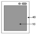
도 2는 본 출원의 일 구현예에 따라 기판(40)에 이형 필름(10)을 부착한 후에 패턴 형성부의 이형 필름을 제거한 것을 나타낸 것이다.2 shows the release film of the pattern forming portion removed after the
본 출원의 일 구현예에서 상기 이형 필름의 두께는 100㎛ 이하, 구체적으로 1㎛ ~ 50㎛, 더욱 구체적으로 1㎛ ~ 30㎛ 일 수 있다. 100㎛ 이하인 것이 패턴 가장자리의 선명도(sharpness)를 높이기 위해서 바람직하다. 1㎛ 이상인 것이 인쇄시의 인쇄 조성물에 대한 내용제성 특성이 우수하다.In one embodiment of the present application, the thickness of the release film may be 100 占 퐉 or less, specifically 1 占 퐉 to 50 占 퐉, more specifically 1 占 퐉 to 30 占 퐉. It is preferable that the thickness is 100 μm or less in order to increase the sharpness of the pattern edge. 1 占 퐉 or more is excellent in solvent resistance property to the printing composition at the time of printing.
본 출원의 일 구현예에서 상기 이형 필름은 기재 필름; 및 점착제층을 포함할수 있다.In one embodiment of the present application, the release film comprises a substrate film; And a pressure-sensitive adhesive layer.
본 출원의 일 구현예에 따르면, 상기 기재 필름은 플라스틱 필름일 수 있다. 구체적으로 폴리에스테르계, 폴리올레핀계, 폴리이미드계, 나일론계 또는 이들의 혼합 수지 필름일 수 있고, 더욱 구체적으로 폴리에틸렌테레프탈레이트(Polyethyleneterephthalate; PET), 폴리부틸렌테레프탈레이트(Poly butyleneterephthalate; PBT), 폴리에틸렌 나프탈레이트(Polyethylenenaphthalate; PEN), 폴리부틸렌나프탈레이트(Polybutylenenaphthalate; PBN), 폴리에틸렌(poly etylene; PE), 폴리프로필렌(Polypropylene;PP), 폴리이미드(Polyimide: PI), 나일론(Nylon) 및 이들의 혼합 수지로 이루어진 군에서 선택되는 필름일 수 있다.According to one embodiment of the present application, the base film may be a plastic film. Specifically, it may be a polyester-based, polyolefin-based, polyimide-based, nylon-based or a mixed resin film thereof, and more specifically, polyethylene terephthalate (PET), poly butylene terephthalate (PBT), polyethylene Naphthalate (Polyethylenenaphthalate (PEN), Polybutylenenaphthalate (PBN), Poly (ethylene) (PE), Polypropylene (PP), Polyimide (PI), Nylon (Nylon) and mixtures thereof It may be a film selected from the group consisting of resins.
본 출원의 일 구현예에서 상기 점착제층은 인쇄시에 인쇄용 조성물이 보호 필름 내측에 침투하지 않기 위한 내용제성, 내화학성 및 내오일성을 가져야 한다. 예를 들어, 점착제층은 아크릴계, 실리콘계 또는 우레탄계 점착제를 사용할 수 있다.In one embodiment of the present application, the pressure-sensitive adhesive layer should have solvent resistance, chemical resistance and oil resistance so that the printing composition does not penetrate inside the protective film at the time of printing. For example, the pressure-sensitive adhesive layer may employ an acrylic, silicone or urethane pressure-sensitive adhesive.
본 출원의 일 구현예에서 상기 패턴 미형성부는 유효 화면부, 센서부, 카메라부, 로고부, 버튼부 및 오픈부로 이루어진 군에서 선택되는 하나 또는 둘 이상을 포함하는 부분일 수 있다.In one embodiment of the present invention, the non-pattern forming portion may be a portion including one or more selected from the group consisting of an effective screen portion, a sensor portion, a camera portion, a logo portion, a button portion and an open portion.
본 출원의 일 구현예에서 상기 베젤 패턴 형성 방법은 하나의 기판에 하나의 베젤 패턴을 인쇄하기 위한 방법일 수 있고, 하나의 기판에 둘 이상의 베젤 패턴을 인쇄하기 위한 방법일 수도 있다.In one embodiment of the present application, the bezel pattern forming method may be a method for printing one bezel pattern on one substrate, or a method for printing two or more bezel patterns on one substrate.
본 출원의 일 구현예에서 하나의 기판에 하나의 베젤 패턴을 인쇄하는 경우 이형 필름을 미리 재단된 기판에 부착할 수 있다. 이 경우 이형 필름을 부착하는 단계에서 얼라인먼트(alignment)의 추가 공정이 필요할 수 있다.In one embodiment of the present application, if a single bezel pattern is printed on one substrate, the release film can be attached to the previously cut substrate. In this case, an additional step of alignment may be required in the step of attaching the release film.
본 출원의 일 구현예에서 하나의 기판에 하나의 베젤 패턴을 인쇄하는 경우 이형 필름을 기판에 부착하는 단계에서 미리 재단되지 않은 기판을 사용할 수도 있다. 이 경우 베젤 패턴을 인쇄하는 단계 이후에, 베젤 패턴 형태에 따라 기판을 재단하는 단계를 더 포함할 수 있다.In one embodiment of the present application, when a single bezel pattern is printed on one substrate, a substrate not previously cut may be used in attaching the release film to the substrate. In this case, after the step of printing the bezel pattern, it may further include cutting the substrate according to the bezel pattern shape.
본 출원의 일 구현예에 따르면, 하나의 기판에 둘 이상의 베젤 패턴을 인쇄하기 위하여, 상기 베젤 패턴을 인쇄하는 단계 이후에, 베젤 패턴 형태에 따라 기판을 재단하는 단계를 더 포함할 수 있다.According to an embodiment of the present application, in order to print two or more bezel patterns on one substrate, after the step of printing the bezel pattern, cutting the substrate according to the bezel pattern shape may be further included.
본 출원의 일 구현예에 따른 상기 베젤 패턴 형성 방법은 상기 베젤 패턴을 인쇄하는 단계 이후에, 베젤 패턴 형태에 따라 기판을 재단하는 단계를 거친 후에 기판에서 이형 필름을 제거하는 단계를 포함할 수 있다.The bezel pattern forming method according to an embodiment of the present application may include a step of removing the release film from the substrate after the step of cutting the substrate according to the bezel pattern shape after the step of printing the bezel pattern .
본 출원의 일 구현예에 따른 상기 베젤 패턴 형성 방법은 상기 베젤 패턴을 인쇄하는 단계 이후에, 기판에서 이형 필름을 제거하는 단계를 거친 후에 베젤 패턴 형태에 따라 기판을 재단하는 단계를 포함할 수 있다.The bezel pattern forming method according to an embodiment of the present application may include cutting the substrate according to the bezel pattern shape after the step of removing the release film from the substrate after printing the bezel pattern .
도 3은 한 기판에 여러 개의 베젤 패턴을 인쇄하기 위한 기판을 나타낸 것이다. 도 3의 경우와 같이 베젤 패턴을 인쇄한 이후에 베젤 패턴 형태에 따라 각각의 기판으로 재단하는 경우에는 얼라인먼트(alignment)의 추가 공정이 필요하지 않는다는 장점이 있다.3 shows a substrate for printing several bezel patterns on one substrate. 3, there is an advantage that an additional alignment process is not required when the bezel pattern is cut into individual substrates according to the bezel pattern shape after printing.
본 출원의 일 구현예에 따른 베젤 패턴을 인쇄하는 단계에서는 기판의 전면 또는 부분에 잉크 조성물을 도포할 수 있다.In the step of printing the bezel pattern according to an embodiment of the present application, the ink composition may be applied to the front surface or the part of the substrate.
본 출원의 일 구현예에 따른 베젤 패턴을 인쇄하는 단계에서 인쇄된 패턴의 선고(높이)는 0.5 ㎛ ~ 10 ㎛, 구체적으로 0.5 ㎛ ~ 5㎛ 일 수 있다. 종래의 스크린 인쇄 방법을 사용하여 베젤 패턴을 인쇄하는 경우에는 베젤 패턴의 선고가 20㎛ 이상이 되므로 단차가 높다. 그러므로 높은 단차에 의해 크랙(crack)이 발생하는 경우가 많아서, 디스플레이의 성능이 떨어질 수 있는 단점이 있다. 그러나, 본 출원의 방법을 사용하는 경우는 0.5 ㎛ ~ 10 ㎛의 선고를 구현할 수 있으므로, 크랙이 거의 발생하지 않게 되어 디스플레이의 성능을 향상시킬 수 있는 장점이 있다.In the step of printing the bezel pattern according to an embodiment of the present invention, the printed height (height) of the printed pattern may be 0.5 μm to 10 μm, specifically 0.5 μm to 5 μm. In the case of printing a bezel pattern using a conventional screen printing method, the pitch of the bezel pattern is 20 占 퐉 or more, so that the step is high. Therefore, cracks often occur due to a high level difference, which may deteriorate display performance. However, in the case of using the method of the present invention, it is possible to implement a detection of 0.5 μm to 10 μm, so that cracks hardly occur and the performance of the display can be improved.
본 출원의 일 구현예에 따른 베젤 패턴을 인쇄하는 단계에서 인쇄 방법은 특별히 제한되지 않는다. 구체적으로 스핀(Spin) 코팅, 리버스 오프셋(Reverse Offset), 잉크젯(Ink Jet) 인쇄, 그라비아(Gravure) 코팅, 마이크로 그라비아(Micro Gravure) 코팅, 키스 그라비아(Kiss Gravure) 코팅, 콤마 나이프(Comma Knife) 코팅, 롤(Roll) 코팅, 스프레이(Spray) 코팅, 메이어 바(Meyer Bar) 코팅 및 슬릿 다이(Slit Die) 코팅으로 이루어진 군에서 선택된 방법을 사용할 수 있다.The printing method in the step of printing the bezel pattern according to an embodiment of the present application is not particularly limited. Specifically, spin coating, reverse offset, ink jet printing, gravure coating, micro gravure coating, kis gravure coating, comma knife The method selected from the group consisting of coating, roll coating, spray coating, mayer bar coating and slit die coating can be used.
본 출원의 일 구현예에 따른 기판에서 이형 필름을 제거하는 단계는 패턴 미형성부의 이형 필름을 제거하는 단계일 수 있다. 구체적으로 인쇄 후에 남아 있는 이형 필름을 기계적으로 제거하거나 접착 테이프에 붙여서 제거하거나 특정 용매에 담그어서 제거할 수 있다. 또는 인쇄 후에 남아 있는 이형 필름에 열을 가하는 방법, 레이저를 조사하는 방법 또는 UV를 조사하는 방법을 사용할 수 있다.The step of removing the release film from the substrate according to an embodiment of the present application may be a step of removing the release film of the patterned amorphous portion. Specifically, the release film remaining after printing may be mechanically removed or adhered to an adhesive tape, or may be removed by immersing it in a specific solvent. A method of applying heat to the release film remaining after printing, a method of irradiating a laser, or a method of irradiating UV can be used.
도 4는 본 출원의 일 구현예에 따라 인쇄 후에 이형 필름을 제거한 인쇄물인 베젤 패턴을 나타낸 것이다.Figure 4 shows a bezel pattern as a printed product with the release film removed after printing according to one embodiment of the present application.
본 출원의 일 구현예는 상기 디스플레이 기판의 베젤 패턴 형성 방법에 사용되는 이형 필름을 제공한다.One embodiment of the present application provides a release film used in a method of forming a bezel pattern of the display substrate.
본 출원의 일 구현예는 패턴 미형성부를 포함하는 디스플레이 기판의 베젤 패턴 형성용 이형 필름을 제공한다. 상기 이형 필름은 패턴 형성부를 더 포함하고, 패턴 형성부는 패턴 미형성부와 분리 가능한 형태일 수 있다. 상기 이형 필름에 대한 설명은 상술한 바와 같다.One embodiment of the present application provides a release film for forming a bezel pattern of a display substrate comprising a pattern unformed portion. The release film may further include a pattern forming portion, and the pattern forming portion may be in a form detachable from the pattern forming portion. The description of the release film is as described above.
본 출원의 일 구현예는 상기 이형 필름을 포함하는 디스플레이 기판을 제공한다.One embodiment of the present application provides a display substrate comprising the release film.
상기 디스플레이 기판은 플라즈마 디스플레이 패널(Plasma Display Panel, PDP), 액정 디스플레이(Liquid Crystal Display, LCD) 패널, 전기영동 디스플레이 (Electrophoretic display) 패널 및 음극선관(Cathode-Ray Tube, CRT) 패널, OLED 디스플레이 패널 또는 각종 터치 패널 등을 포함한다.The display substrate may include a plasma display panel (PDP), a liquid crystal display (LCD) panel, an electrophoretic display panel, a cathode ray tube (CRT) panel, an OLED display panel Or various kinds of touch panels.
본 출원의 일 구현예는 상기 이형 필름을 이용하여 제조된 디스플레이 기판을 포함하는 전자 소자를 제공한다.One embodiment of the present application provides an electronic device comprising a display substrate made using the release film.
이하 실시예 및 비교예를 통하여 본 출원을 더욱 상세하게 설명한다. 그러나, 이하의 실시예 및 비교예는 본 출원을 예시하기 위한 것이며, 이에 의하여 본 출원의 범위가 한정되는 것은 아니다.
Hereinafter, the present application will be described in more detail with reference to Examples and Comparative Examples. However, the following examples and comparative examples are intended to illustrate the present application, and the scope of the present application is not limited thereby.
<실시예 1>≪ Example 1 >
글라스(glass)의 패턴 형성면에 미리 재단된 두께 20㎛의 이형 필름을 부착한, 후 패턴 형성부의 이형 필름을 제거하였다. 이때 패턴 형성부의 이형 필름을 접착 테이프에 붙여서 제거하는 방법을 사용하였다. 스핀 코터를 사용하여 이형 필름이 부착된 인쇄물에 전면 코팅을 실시하였다. 이때 패턴의 선고는 1㎛ 로 측정되었다. 그리고 나서 패턴 미형성부의 이형 필름을 제거하였다. 이때 패턴 미형성부의 이형 필름을 접착 테이프에 붙여서 제거하는 방법을 사용하였다. 실시예 1에 따라 인쇄된 베젤 패턴을 도 5에 나타내었다.
A release film having a thickness of 20 mu m previously cut and previously cut was adhered to the pattern formation surface of the glass, and the release film of the post pattern formation portion was removed. At this time, a method of attaching the release film of the pattern forming portion to the adhesive tape and removing the release film was used. The printed matter having the release film attached thereto was subjected to a front coating using a spin coater. At this time, the pattern was measured at 1 μm. Then, the release film of the pattern micropattern was removed. At this time, a method of attaching the release film of the pattern unhardened portion to the adhesive tape to remove it was used. A bezel pattern printed according to Example 1 is shown in Fig.
<실시예 2><Example 2>
글라스(glass)의 패턴 형성면에 미리 재단된 두께 20㎛의 이형 필름을 부착한, 후 패턴 형성부의 이형 필름을 제거하였다. 이때 패턴 형성부의 이형 필름을 접착 테이프에 붙여서 제거하는 방법을 사용하였다. 실리콘 블랭킷에 메이어 바(mayer bar)를 사용하여 인쇄물질을 전면 코팅하였다. 인쇄물질이 전면 코팅된 블랭킷을 이형 필름이 부착된 글래스의 패턴 형성면에 접촉하여 전사하였다. 이때 패턴의 선고는 1㎛ 로 측정되었다. 그리고 나서 패턴 미형성부의 이형 필름을 제거하였다. 이때 패턴 미형성부의 이형 필름을 접착 테이프에 붙여서 제거하는 방법을 사용하였다. 실시예 2에 따라 인쇄된 베젤 패턴을 도 6에 나타내었다.
A release film having a thickness of 20 mu m previously cut and previously cut was adhered to the pattern formation surface of the glass, and the release film of the post pattern formation portion was removed. At this time, a method of attaching the release film of the pattern forming portion to the adhesive tape and removing the release film was used. The printing material was coated on the silicon blanket using a mayer bar. The blanket with the printing material coated on the front side was transferred in contact with the pattern forming surface of the glass having the releasing film attached thereto. At this time, the pattern was measured at 1 μm. Then, the release film of the pattern micropattern was removed. At this time, a method of attaching the release film of the pattern unhardened portion to the adhesive tape to remove it was used. A bezel pattern printed according to Example 2 is shown in Fig.
<실시예 3><Example 3>
글라스(glass)의 패턴 형성면에 미리 재단된 두께 20㎛의 이형 필름을 부착한, 후 패턴 형성부의 이형 필름을 제거하였다. 이때 패턴 형성부의 이형 필름을 접착 테이프에 붙여서 제거하는 방법을 사용하였다. 실리콘 블랭킷에 오프셋(off set) 장비를 사용하여 인쇄물질을 전면 도포한 후 인쇄물질이 도포된 블랭킷을 이형 필름이 부착된 글래스의 패턴 형성면에 접촉하여 전사하였다. 이때 패턴의 선고는 0.5㎛ 로 측정되었다. 그리고 나서 패턴 미형성부의 이형 필름을 제거하였다. 이때 패턴 미형성부의 이형 필름을 접착 테이프에 붙여서 제거하는 방법을 사용하였다. 실시예 3에 따라 인쇄된 베젤 패턴을 도 7에 나타내었다. 스핀 코팅 방법을 사용한 실시예 1 또는 메이어 바 코팅 방법을 사용한 실시예 2에 비하여 더 선명한 베젤 패턴이 형성된 것을 확인할 수 있었다.
A release film having a thickness of 20 mu m previously cut and previously cut was adhered to the pattern formation surface of the glass, and the release film of the post pattern formation portion was removed. At this time, a method of attaching the release film of the pattern forming portion to the adhesive tape and removing the release film was used. After the printing material was entirely coated on the silicon blanket using an off set equipment, the blanket having the printing material applied thereto was transferred in contact with the pattern forming surface of the glass having the releasing film attached thereto. At this time, the test pattern was measured to be 0.5 mu m. Then, the release film of the pattern micropattern was removed. At this time, a method of attaching the release film of the pattern unhardened portion to the adhesive tape to remove it was used. A bezel pattern printed according to Example 3 is shown in Fig. It was confirmed that a clearer bezel pattern was formed as compared with Example 1 using the spin coating method or Example 2 using the Meyer Bar coating method.
<비교예 1>≪ Comparative Example 1 &
글라스(glass)에 스크린 인쇄 방법을 통하여 베젤 패턴을 형성하였다. 이때 패턴의 선고는 15㎛ 로 측정되었다.A bezel pattern was formed on a glass through a screen printing method. At this time, the pattern was measured at 15 μm.
패턴의 선고가 높은 경우 그 단차로 인해 단락이 발생하고 크랙이 발생하여 내구성이 떨어진다. 또한, 단차를 개선하기 위해 광학 점착제를 사용할 수도 있는데, 이때 제품의 두께가 두꺼워져서 외관상 둔탁해 보이는 문제가 있다.If the pattern is high, short circuit occurs due to the step, and cracks occur, resulting in poor durability. In addition, an optical adhesive may be used to improve the level difference. In this case, the thickness of the product becomes thick, which is apparently a blurred appearance.
또한, 패널과 각종 필름의 라미네이션 작업시에 패턴 선고로 인해 발생하는 단차로 인해 기포가 발생할 수 있다. 기포가 발생하면 기포를 제거하기 위해 고온, 고압의 공정을 요구할 수 있고, 고온, 고압에서도 기포가 제거되지 않을 수도 있어서, 문제가 있다.Further, bubbles may be generated due to a step generated due to patterning during lamination of the panel and various films. If bubbles are generated, a high-temperature and high-pressure process may be required to remove bubbles, and bubbles may not be removed even at high temperatures and high pressures.
본 출원이 속한 분야에서 통상의 지식을 가진 자라면 상기 내용을 바탕으로 본 출원의 범주 내에서 다양한 응용 및 변형을 행하는 것이 가능할 것이다.It will be understood by those skilled in the art that various changes in form and details may be made therein without departing from the spirit and scope of the invention as defined by the appended claims.
이상으로 본 출원의 특정한 부분을 상세히 기술하였는 바, 당업계의 통상의 지식을 가진 자에게 있어서 이러한 구체적인 기술은 단지 바람직한 구현예일 뿐이며, 이에 본 출원의 범위가 제한되는 것이 아닌 점은 명백하다. 따라서, 본 출원의 실질적인 범위는 첨부된 청구항과 그의 등가물에 의하여 정의된다고 할 것이다.Having described specific portions of the present application in detail, those skilled in the art will appreciate that these specific embodiments are merely preferred embodiments and that the scope of the present application is not limited thereto. Accordingly, the actual scope of the present application will be defined by the appended claims and their equivalents.
10: 이형 필름
20: 패턴 형성부
30: 패턴 미형성부
40: 기판
10: release film
20:
30: Pattern morphology
40: substrate
Claims (19)
Translated fromKorean기판에 잉크 조성물을 도포하여 적어도 하나의 베젤 패턴을 인쇄하는 단계; 및
기판에서 이형 필름을 제거하는 단계를 포함하는 디스플레이 기판의 베젤 패턴 형성 방법.Attaching a release film having a pattern-forming portion and having a cohesive force to a substrate;
Applying an ink composition to a substrate to print at least one bezel pattern; And
Removing the release film from the substrate.
상기 베젤 패턴을 인쇄하는 단계 이후에,
베젤 패턴 형태에 따라 기판을 재단하는 단계를 더 포함하는 것을 특징으로 하는 디스플레이 기판의 베젤 패턴 형성 방법.The method according to claim 1,
After printing the bezel pattern,
Further comprising the step of cutting the substrate according to the bezel pattern shape.
상기 이형 필름은 패턴 형성부를 더 포함하고,
패턴 형성부는 패턴 미형성부와 분리 가능한 형태인 것을 특징으로 하는 디스플레이 기판의 베젤 패턴 형성 방법.The method according to claim 1,
The release film further includes a pattern forming unit,
A method of forming a bezel pattern of a display substrate, characterized in that the pattern forming portion is separated from the pattern non-forming portion.
이형 필름을 기판에 부착하는 단계 이후에,
기판에서 패턴 형성부의 이형 필름을 제거하는 단계를 더 포함하는 것을 특징으로 하는 디스플레이 기판의 베젤 패턴 형성 방법.The method according to claim 3,
After the step of attaching the release film to the substrate,
And removing the release film of the pattern forming portion from the substrate.
상기 이형 필름은 패턴 미형성부의 점착력이 패턴 형성부의 점착력과 같거나 큰 것을 특징으로 하는 디스플레이 기판의 베젤 패턴 형성 방법.The method according to claim 3,
Wherein the releasing film has an adhesive force of the patterned portion is equal to or greater than an adhesive force of the patterned portion.
상기 패턴 형성부의 이형 필름의 제거는 열을 가하는 방법, 레이저를 조사하는 방법 또는 UV를 조사하는 방법을 사용하는 것을 특징으로 하는 디스플레이 기판의 베젤 패턴 형성 방법.The method of claim 4,
Wherein the removal of the release film of the pattern forming portion uses a method of applying heat, a method of irradiating a laser, or a method of irradiating UV.
상기 이형 필름의 두께는 100㎛ 이하인 것을 특징으로 하는 디스플레이 기판의 베젤 패턴 형성 방법.The method according to claim 1,
Wherein the thickness of the release film is 100 占 퐉 or less.
상기 이형 필름은 기재 필름; 및 점착제층을 포함하는 것을 특징으로 하는 디스플레이 기판의 베젤 패턴 형성 방법.The method according to claim 1,
Wherein the release film comprises a base film; And a pressure-sensitive adhesive layer.
상기 기재 필름은 폴리에틸렌테레프탈레이트(Polyethyleneterephthalate; PET), 폴리부틸렌테레프탈레이트(Poly butyleneterephthalate; PBT), 폴리에틸렌 나프탈레이트(Polyethylenenaphthalate; PEN), 폴리부틸렌나프탈레이트(Polybutylenenaphthalate; PBN), 폴리에틸렌(poly etylene; PE), 폴리프로필렌(Polypropylene;PP), 폴리이미드(Polyimide: PI), 나일론(Nylon) 및 이들의 혼합 수지로 이루어진 군에서 선택되는 것을 특징으로 하는 디스플레이 기판의 베젤 패턴 형성 방법.The method according to claim 8,
The base film is polyethylene terephthalate (PET), polybutylene terephthalate (PBT), polyethylene naphthalate (PEN), polybutylene naphthalate (PBN), polyethylene (poly etylene; PE) ), Polypropylene (PP), polyimide (PI), nylon (Nylon) and a mixed resin thereof.
상기 패턴 미형성부는 유효 화면부, 센서부, 카메라부, 로고부, 버튼부 및 오픈부로 이루어진 군에서 선택되는 하나 또는 둘 이상을 포함하는 것을 특징으로 하는 디스플레이 기판의 베젤 패턴 형성 방법.The method according to claim 1,
Wherein the pattern unformed portion includes one or more selected from the group consisting of an effective screen portion, a sensor portion, a camera portion, a logo portion, a button portion, and an open portion.
상기 베젤 패턴을 인쇄하는 단계에서 인쇄된 패턴의 선고는 0.5㎛ ~ 10㎛ 인 것을 특징으로 하는 디스플레이 기판의 베젤 패턴 형성 방법.The method according to claim 1,
Wherein the pattern of the printed pattern in the step of printing the bezel pattern is 0.5 占 퐉 to 10 占 퐉.
상기 베젤 패턴을 인쇄하는 단계에서 인쇄 방법은 스핀(Spin) 코팅, 리버스 오프셋(Reverse Offset), 잉크젯(Ink Jet) 인쇄, 스크린(Screen) 인쇄, 그라비아(Gravure) 코팅, 마이크로 그라비아(Micro Gravure) 코팅, 키스 그라비아(Kiss Gravure) 코팅, 콤마 나이프(Comma Knife) 코팅, 롤(Roll) 코팅, 스프레이(Spray) 코팅, 메이어 바(Meyer Bar) 코팅 및 슬릿 다이(Slit Die) 코팅으로 이루어진 군에서 선택된 것을 특징으로 하는 특징으로 하는 디스플레이 기판의 베젤 패턴 형성 방법.The method according to claim 1,
The printing method in the step of printing the bezel pattern is spin coating, reverse offset, ink jet printing, screen printing, gravure coating, micro gravure coating Selected from the group consisting of Keith Gravure coating, Comma Knife coating, Roll coating, Spray coating, Meyer Bar coating and Slit Die coating A method for forming a bezel pattern of a display substrate, characterized by the above-mentioned.
상기 패턴 미형성부는 유효화면부, 센서부, 카메라부, 로고부, 버튼부 및 오픈부로 이루어진 군에서 선택되는 하나 또는 둘 이상을 포함하는 것을 특징으로 하는 이형 필름.The method according to claim 14,
Wherein the pattern unformed portion includes one or more selected from the group consisting of an effective screen portion, a sensor portion, a camera portion, a logo portion, a button portion, and an open portion.
상기 이형 필름은 패턴 형성부를 더 포함하고,
패턴 형성부는 패턴 미형성부와 분리 가능한 형태인 것을 특징으로 하는 이형 필름.The method according to claim 14,
The release film further includes a pattern forming unit,
The pattern forming part is a release film, characterized in that the form is separated from the pattern unformed part.
상기 이형 필름은 패턴 미형성부의 점착력이 패턴 형성부의 점착력과 같거나 큰 것을 특징으로 하는 이형 필름.18. The method of claim 16,
Wherein the releasing film has the same adhesive force as that of the pattern forming portion, and the adhesive force of the pattern releasing portion is equal to or larger than the adhesive force of the pattern forming portion.
An electronic device comprising a display substrate manufactured using the release film of claim 14.
Priority Applications (1)
| Application Number | Priority Date | Filing Date | Title |
|---|---|---|---|
| TW102124497ATWI541719B (en) | 2012-07-11 | 2013-07-09 | Method for forming bezel pattern of display panel |
Applications Claiming Priority (2)
| Application Number | Priority Date | Filing Date | Title |
|---|---|---|---|
| KR1020120075670 | 2012-07-11 | ||
| KR20120075670 | 2012-07-11 |
Publications (2)
| Publication Number | Publication Date |
|---|---|
| KR20140009035Atrue KR20140009035A (en) | 2014-01-22 |
| KR101468814B1 KR101468814B1 (en) | 2014-12-08 |
Family
ID=49916274
Family Applications (1)
| Application Number | Title | Priority Date | Filing Date |
|---|---|---|---|
| KR1020130079260AActiveKR101468814B1 (en) | 2012-07-11 | 2013-07-05 | Method for forming bezel patten of display panel |
Country Status (7)
| Country | Link |
|---|---|
| US (2) | US9381534B2 (en) |
| EP (1) | EP2874137B1 (en) |
| JP (1) | JP5822371B2 (en) |
| KR (1) | KR101468814B1 (en) |
| CN (1) | CN104040614B (en) |
| TW (1) | TWI541719B (en) |
| WO (1) | WO2014010884A1 (en) |
Cited By (11)
| Publication number | Priority date | Publication date | Assignee | Title |
|---|---|---|---|---|
| JP2016027393A (en)* | 2014-06-27 | 2016-02-18 | 日東電工株式会社 | Long polarizing film laminate |
| WO2016076662A1 (en)* | 2014-11-13 | 2016-05-19 | 주식회사 엘지화학 | Ultraviolet curable white ink composition for inkjet printing, method for preparing white bezel pattern using same, and electronic device comprising white bezel pattern prepared by same |
| KR20160147535A (en) | 2015-06-15 | 2016-12-23 | 주식회사 엘지화학 | Method for forming a bezel pattern, a bezel pattern formed thereby and panel comprising the bezel pattern |
| JP2017068244A (en)* | 2015-09-30 | 2017-04-06 | 日東電工株式会社 | Method and device for inspecting polarizing plate |
| US9963602B2 (en) | 2014-11-13 | 2018-05-08 | Lg Chem, Ltd. | Ultraviolet curable white ink composition for inkjet printing, method for preparing white bezel pattern using same, and electronic device comprising white bezel pattern prepared by same |
| US10234611B2 (en) | 2015-09-28 | 2019-03-19 | Nitto Denko Corporation | Polarizer, polarizing plate, and image display apparatus |
| US10754072B2 (en) | 2014-06-27 | 2020-08-25 | Nitto Denko Corporation | Polarizer having non-polarization portions, a long polarizing plate and image display device comprising the polarizer |
| JP2020144387A (en)* | 2014-06-27 | 2020-09-10 | 日東電工株式会社 | Long polarizing film laminate |
| US10782462B2 (en) | 2014-04-25 | 2020-09-22 | Nitto Denko Corporation | Polarizer, polarizing plate, and image display apparatus |
| US11061176B2 (en) | 2014-04-25 | 2021-07-13 | Nitto Denko Corporation | Polarizer, polarizing plate, and image display apparatus |
| US11467328B2 (en) | 2015-06-25 | 2022-10-11 | Nitto Denko Corporation | Polarizer having non-polarizing part |
Families Citing this family (11)
| Publication number | Priority date | Publication date | Assignee | Title |
|---|---|---|---|---|
| WO2016048118A1 (en)* | 2014-09-26 | 2016-03-31 | 주식회사 엘지화학 | Uv-curable ink composition, method for producing bezel pattern of display substrate using same, and bezel pattern produced thereby |
| WO2016048115A1 (en)* | 2014-09-26 | 2016-03-31 | 주식회사 엘지화학 | Uv-curable ink composition, method for producing bezel pattern of display substrate using same, and bezel pattern produced thereby |
| WO2016048116A1 (en)* | 2014-09-26 | 2016-03-31 | 주식회사 엘지화학 | Uv-curable ink composition, method for producing bezel pattern of display substrate using same, and bezel pattern produced thereby |
| US10259957B2 (en) | 2014-09-26 | 2019-04-16 | Lg Chem, Ltd. | UV-curable ink composition, method for producing bezel pattern of display substrate using same, and bezel pattern produced thereby |
| WO2016048120A1 (en)* | 2014-09-26 | 2016-03-31 | 주식회사 엘지화학 | Uv-curable ink composition, method for producing bezel pattern of display substrate using same, and bezel pattern produced thereby |
| WO2016048117A1 (en)* | 2014-09-26 | 2016-03-31 | 주식회사 엘지화학 | Uv-curable ink composition, method for producing bezel pattern of display substrate using same, and bezel pattern produced thereby |
| WO2016048119A1 (en)* | 2014-09-26 | 2016-03-31 | 주식회사 엘지화학 | Uv-curable ink composition, method for producing bezel pattern of display substrate using same, and bezel pattern produced thereby |
| KR102067857B1 (en)* | 2016-04-08 | 2020-01-17 | 주식회사 엘지화학 | A method for forming a bezel pattern using inkjet printing |
| KR102090577B1 (en) | 2016-10-17 | 2020-03-18 | 엘지전자 주식회사 | Printing Apparatus |
| KR102197892B1 (en)* | 2016-12-09 | 2021-01-04 | 주식회사 엘지화학 | Method for forming UV pattern using inkjet printing, method for preparing bezel including the same and bezel prepared thereby |
| CN108745816B (en)* | 2018-06-12 | 2021-12-03 | 业成科技(成都)有限公司 | Gluing method |
Family Cites Families (25)
| Publication number | Priority date | Publication date | Assignee | Title |
|---|---|---|---|---|
| US2547674A (en)* | 1946-06-12 | 1951-04-03 | Brady Co W H | Stencil |
| JPH02127062U (en) | 1989-03-29 | 1990-10-19 | ||
| JPH0595178A (en)* | 1991-10-02 | 1993-04-16 | Sharp Corp | Production of circuit board |
| JP2533456B2 (en)* | 1993-06-16 | 1996-09-11 | 日東電工株式会社 | Label and label base material and ink |
| JPH06196845A (en) | 1993-10-01 | 1994-07-15 | Aiwa Co Ltd | Manufacture of simple printed board |
| JP3441150B2 (en)* | 1994-04-13 | 2003-08-25 | 理想科学工業株式会社 | Heat-sensitive stencil paper |
| JPH11129640A (en)* | 1997-11-04 | 1999-05-18 | Sumitomo Metal Ind Ltd | Printing mask, method of manufacturing the same, and method of manufacturing a circuit board |
| JP2003308016A (en)* | 2002-04-16 | 2003-10-31 | Nitto Denko Corp | Adhesive label for display |
| KR100950134B1 (en)* | 2002-12-27 | 2010-03-30 | 엘지디스플레이 주식회사 | Resist printing cells and manufacturing method |
| US6905751B2 (en)* | 2003-01-22 | 2005-06-14 | Mohawk Brands Inc. | Tile coverings with borders and inserts and methods of installation |
| US20050000642A1 (en)* | 2003-07-03 | 2005-01-06 | 3M Innovative Properties Company | Cling articles |
| US7416977B2 (en)* | 2004-04-28 | 2008-08-26 | Semiconductor Energy Laboratory Co., Ltd. | Method for manufacturing display device, liquid crystal television, and EL television |
| KR100724817B1 (en) | 2006-02-21 | 2007-06-04 | 엘에스전선 주식회사 | Screen printing method |
| KR100690929B1 (en) | 2006-05-03 | 2007-03-09 | 한국기계연구원 | High resolution pattern formation method having desired pattern thickness or high aspect ratio using dry film resist |
| WO2008032476A1 (en)* | 2006-09-11 | 2008-03-20 | Sharp Kabushiki Kaisha | Display device provided with touch panel |
| BRPI0718394A2 (en)* | 2006-11-02 | 2013-11-26 | Nissha Printing | EQUIPMENT PROTECTED PANEL WITH TOUCH INPUT FUNCTION FOR ELECTRONIC DEVICE DISPLAY WINDOW |
| KR20080090694A (en) | 2007-04-05 | 2008-10-09 | 박윤희 | Manufacturing method of a die-free cell phone keypad and a manufacturing method of a die-free cell phone keypad manufacturing method and a method of manufacturing a keypad and keypad manufactured by the manufacturing disc |
| US20090053485A1 (en) | 2007-08-24 | 2009-02-26 | Melanie Royals | Surface Decoration System |
| US8399356B2 (en)* | 2008-03-28 | 2013-03-19 | Semiconductor Energy Laboratory Co., Ltd. | Manufacturing method of semiconductor device |
| JP2011014286A (en) | 2009-06-30 | 2011-01-20 | Hitachi Ltd | Plasma display panel and method of manufacturing the same, and plasma display device |
| JP2011114286A (en)* | 2009-11-30 | 2011-06-09 | Asahi Glass Co Ltd | Method of manufacturing substrate with conductive pattern |
| KR101156771B1 (en) | 2010-08-26 | 2012-06-18 | 삼성전기주식회사 | Method of manufacturing conductive transparent substrate |
| KR101379901B1 (en) | 2010-08-31 | 2014-04-01 | 한국기계연구원 | Method of fabricating fine pattern on substrate using solid film barrier |
| JP6035734B2 (en)* | 2011-06-20 | 2016-11-30 | ソニー株式会社 | Semiconductor element, display device and electronic apparatus |
| KR20130027747A (en)* | 2011-09-08 | 2013-03-18 | 삼성전기주식회사 | Touch pannel |
- 2013
- 2013-07-05WOPCT/KR2013/006007patent/WO2014010884A1/enactiveApplication Filing
- 2013-07-05KRKR1020130079260Apatent/KR101468814B1/enactiveActive
- 2013-07-05JPJP2014548701Apatent/JP5822371B2/enactiveActive
- 2013-07-05USUS14/365,010patent/US9381534B2/enactiveActive
- 2013-07-05CNCN201380005208.6Apatent/CN104040614B/enactiveActive
- 2013-07-05EPEP13816327.4Apatent/EP2874137B1/enactiveActive
- 2013-07-09TWTW102124497Apatent/TWI541719B/enactive
- 2015
- 2015-02-18USUS14/625,332patent/US9925553B2/enactiveActive
Cited By (15)
| Publication number | Priority date | Publication date | Assignee | Title |
|---|---|---|---|---|
| US11061176B2 (en) | 2014-04-25 | 2021-07-13 | Nitto Denko Corporation | Polarizer, polarizing plate, and image display apparatus |
| US10782462B2 (en) | 2014-04-25 | 2020-09-22 | Nitto Denko Corporation | Polarizer, polarizing plate, and image display apparatus |
| US10215900B2 (en) | 2014-06-27 | 2019-02-26 | Nitto Denko Corporation | Polarizing film laminate comprising a long polarizing having exposed portion where a polarizer is exposed |
| JP2016027393A (en)* | 2014-06-27 | 2016-02-18 | 日東電工株式会社 | Long polarizing film laminate |
| US10754072B2 (en) | 2014-06-27 | 2020-08-25 | Nitto Denko Corporation | Polarizer having non-polarization portions, a long polarizing plate and image display device comprising the polarizer |
| JP2020144387A (en)* | 2014-06-27 | 2020-09-10 | 日東電工株式会社 | Long polarizing film laminate |
| US11385391B2 (en) | 2014-06-27 | 2022-07-12 | Nitto Denko Corporation | Polarizer having non-polarization portions, a long polarizing plate and image display device comprising the polarizer |
| WO2016076662A1 (en)* | 2014-11-13 | 2016-05-19 | 주식회사 엘지화학 | Ultraviolet curable white ink composition for inkjet printing, method for preparing white bezel pattern using same, and electronic device comprising white bezel pattern prepared by same |
| US9963602B2 (en) | 2014-11-13 | 2018-05-08 | Lg Chem, Ltd. | Ultraviolet curable white ink composition for inkjet printing, method for preparing white bezel pattern using same, and electronic device comprising white bezel pattern prepared by same |
| KR20160147535A (en) | 2015-06-15 | 2016-12-23 | 주식회사 엘지화학 | Method for forming a bezel pattern, a bezel pattern formed thereby and panel comprising the bezel pattern |
| US11467328B2 (en) | 2015-06-25 | 2022-10-11 | Nitto Denko Corporation | Polarizer having non-polarizing part |
| US10234611B2 (en) | 2015-09-28 | 2019-03-19 | Nitto Denko Corporation | Polarizer, polarizing plate, and image display apparatus |
| JP2021012392A (en)* | 2015-09-30 | 2021-02-04 | 日東電工株式会社 | Polarizing plate inspection method and inspection equipment |
| JP2021012393A (en)* | 2015-09-30 | 2021-02-04 | 日東電工株式会社 | Polarizing plate inspection method and inspection equipment |
| JP2017068244A (en)* | 2015-09-30 | 2017-04-06 | 日東電工株式会社 | Method and device for inspecting polarizing plate |
Also Published As
| Publication number | Publication date |
|---|---|
| JP2015504245A (en) | 2015-02-05 |
| EP2874137A1 (en) | 2015-05-20 |
| US20140342129A1 (en) | 2014-11-20 |
| CN104040614A (en) | 2014-09-10 |
| JP5822371B2 (en) | 2015-11-24 |
| EP2874137A4 (en) | 2015-12-16 |
| US9925553B2 (en) | 2018-03-27 |
| US20150158046A1 (en) | 2015-06-11 |
| KR101468814B1 (en) | 2014-12-08 |
| WO2014010884A1 (en) | 2014-01-16 |
| TW201415356A (en) | 2014-04-16 |
| CN104040614B (en) | 2017-05-03 |
| US9381534B2 (en) | 2016-07-05 |
| EP2874137B1 (en) | 2021-03-03 |
| TWI541719B (en) | 2016-07-11 |
Similar Documents
| Publication | Publication Date | Title |
|---|---|---|
| KR101468814B1 (en) | Method for forming bezel patten of display panel | |
| US11991894B2 (en) | Flexible display device and method for preparing the same | |
| US11342541B2 (en) | Method of fabricating light emitting display panel using solvent vapor compensation reservoir | |
| JP6035599B2 (en) | Double-sided adhesive film | |
| TWI717401B (en) | Window substrate integrated with polarizing plate and method of preparing the same | |
| KR20140020196A (en) | Printed matter and method for manufacturing the same | |
| KR101269392B1 (en) | Method for manufacturing surface protection board for liquid crystal display device and method for manufacturing liquid crystal display device | |
| EP2886331B1 (en) | Laminate comprising adhesive layer and method for manufacturing same | |
| US9669603B2 (en) | Film for display window, method of manufacturing the same, display window having the same and method of manufacturing the same | |
| CN103203942B (en) | Method For Manufacturing Protective Plate For Display | |
| KR20090112445A (en) | How to make a screen protector window | |
| KR20130117101A (en) | Double-faced adhesive film for tsp with printing layer and method for manufacturing the same | |
| KR101517697B1 (en) | Method for manufacturing film for transferring printed pattern, film for transferring printed pattern, apparatus for manufacturing the same and method for transferring pattern using the same | |
| JP5282967B2 (en) | Label for plastic molding | |
| CN104054157A (en) | Printing plate for reverse offset printing and its preparation method | |
| US20140248817A1 (en) | Manufacturing method for display device provided with thin film electronic circuit | |
| CN104203572B (en) | In-mold transfer film and method of manufacturing said film | |
| JP2015189114A (en) | Printing plate and method for producing printing plate | |
| CN109166984A (en) | Mask and its manufacturing method for oled panel | |
| JP2010224384A (en) | Method for forming arrangement of microsphere and spacer forming method for color filter for flat panel display using the same | |
| JP4770233B2 (en) | Substrate having light-shielding pattern or light-shielding pattern and coloring pattern, display device, and method of manufacturing substrate having light-shielding pattern or light-shielding pattern and coloring pattern | |
| KR20160121089A (en) | Decoration Sheet for Mobile Device and Method for making thereof | |
| JP2013075383A (en) | Glass base material laminate, glass base material laminate roll, and method of manufacturing glass base material laminate | |
| JP2016151587A (en) | Thermosensitive adhesive label | |
| JP2007178874A (en) | Label sheet for laser printer and its manufacturing method |
Legal Events
| Date | Code | Title | Description |
|---|---|---|---|
| A201 | Request for examination | ||
| PA0109 | Patent application | St.27 status event code:A-0-1-A10-A12-nap-PA0109 | |
| PA0201 | Request for examination | St.27 status event code:A-1-2-D10-D11-exm-PA0201 | |
| PG1501 | Laying open of application | St.27 status event code:A-1-1-Q10-Q12-nap-PG1501 | |
| D13-X000 | Search requested | St.27 status event code:A-1-2-D10-D13-srh-X000 | |
| D14-X000 | Search report completed | St.27 status event code:A-1-2-D10-D14-srh-X000 | |
| PE0902 | Notice of grounds for rejection | St.27 status event code:A-1-2-D10-D21-exm-PE0902 | |
| E13-X000 | Pre-grant limitation requested | St.27 status event code:A-2-3-E10-E13-lim-X000 | |
| P11-X000 | Amendment of application requested | St.27 status event code:A-2-2-P10-P11-nap-X000 | |
| P13-X000 | Application amended | St.27 status event code:A-2-2-P10-P13-nap-X000 | |
| E701 | Decision to grant or registration of patent right | ||
| PE0701 | Decision of registration | St.27 status event code:A-1-2-D10-D22-exm-PE0701 | |
| PR0701 | Registration of establishment | St.27 status event code:A-2-4-F10-F11-exm-PR0701 | |
| PR1002 | Payment of registration fee | St.27 status event code:A-2-2-U10-U11-oth-PR1002 Fee payment year number:1 | |
| PG1601 | Publication of registration | St.27 status event code:A-4-4-Q10-Q13-nap-PG1601 | |
| PN2301 | Change of applicant | St.27 status event code:A-5-5-R10-R13-asn-PN2301 St.27 status event code:A-5-5-R10-R11-asn-PN2301 | |
| R18-X000 | Changes to party contact information recorded | St.27 status event code:A-5-5-R10-R18-oth-X000 | |
| FPAY | Annual fee payment | Payment date:20170919 Year of fee payment:4 | |
| PR1001 | Payment of annual fee | St.27 status event code:A-4-4-U10-U11-oth-PR1001 Fee payment year number:4 | |
| FPAY | Annual fee payment | Payment date:20181016 Year of fee payment:5 | |
| PR1001 | Payment of annual fee | St.27 status event code:A-4-4-U10-U11-oth-PR1001 Fee payment year number:5 | |
| R18-X000 | Changes to party contact information recorded | St.27 status event code:A-5-5-R10-R18-oth-X000 | |
| R18-X000 | Changes to party contact information recorded | St.27 status event code:A-5-5-R10-R18-oth-X000 | |
| R18-X000 | Changes to party contact information recorded | St.27 status event code:A-5-5-R10-R18-oth-X000 | |
| FPAY | Annual fee payment | Payment date:20191016 Year of fee payment:6 | |
| PR1001 | Payment of annual fee | St.27 status event code:A-4-4-U10-U11-oth-PR1001 Fee payment year number:6 | |
| PR1001 | Payment of annual fee | St.27 status event code:A-4-4-U10-U11-oth-PR1001 Fee payment year number:7 | |
| PR1001 | Payment of annual fee | St.27 status event code:A-4-4-U10-U11-oth-PR1001 Fee payment year number:8 | |
| PR1001 | Payment of annual fee | St.27 status event code:A-4-4-U10-U11-oth-PR1001 Fee payment year number:9 | |
| PR1001 | Payment of annual fee | St.27 status event code:A-4-4-U10-U11-oth-PR1001 Fee payment year number:10 | |
| PR1001 | Payment of annual fee | St.27 status event code:A-4-4-U10-U11-oth-PR1001 Fee payment year number:11 | |
| PR1001 | Payment of annual fee | St.27 status event code:A-4-4-U10-U11-oth-PR1001 Fee payment year number:12 |