KR20140008983A - 이미지 센서 패키징을 위한 방법 및 장치 - Google Patents
이미지 센서 패키징을 위한 방법 및 장치Download PDFInfo
- Publication number
- KR20140008983A KR20140008983AKR1020120109897AKR20120109897AKR20140008983AKR 20140008983 AKR20140008983 AKR 20140008983AKR 1020120109897 AKR1020120109897 AKR 1020120109897AKR 20120109897 AKR20120109897 AKR 20120109897AKR 20140008983 AKR20140008983 AKR 20140008983A
- Authority
- KR
- South Korea
- Prior art keywords
- bond pad
- array
- bond
- substrate
- pad array
- Prior art date
- Legal status (The legal status is an assumption and is not a legal conclusion. Google has not performed a legal analysis and makes no representation as to the accuracy of the status listed.)
- Ceased
Links
Images


Classifications
- H—ELECTRICITY
- H10—SEMICONDUCTOR DEVICES; ELECTRIC SOLID-STATE DEVICES NOT OTHERWISE PROVIDED FOR
- H10F—INORGANIC SEMICONDUCTOR DEVICES SENSITIVE TO INFRARED RADIATION, LIGHT, ELECTROMAGNETIC RADIATION OF SHORTER WAVELENGTH OR CORPUSCULAR RADIATION
- H10F39/00—Integrated devices, or assemblies of multiple devices, comprising at least one element covered by group H10F30/00, e.g. radiation detectors comprising photodiode arrays
- H10F39/10—Integrated devices
- H10F39/12—Image sensors
- H—ELECTRICITY
- H10—SEMICONDUCTOR DEVICES; ELECTRIC SOLID-STATE DEVICES NOT OTHERWISE PROVIDED FOR
- H10F—INORGANIC SEMICONDUCTOR DEVICES SENSITIVE TO INFRARED RADIATION, LIGHT, ELECTROMAGNETIC RADIATION OF SHORTER WAVELENGTH OR CORPUSCULAR RADIATION
- H10F39/00—Integrated devices, or assemblies of multiple devices, comprising at least one element covered by group H10F30/00, e.g. radiation detectors comprising photodiode arrays
- H10F39/80—Constructional details of image sensors
- H10F39/811—Interconnections
- H—ELECTRICITY
- H01—ELECTRIC ELEMENTS
- H01L—SEMICONDUCTOR DEVICES NOT COVERED BY CLASS H10
- H01L24/00—Arrangements for connecting or disconnecting semiconductor or solid-state bodies; Methods or apparatus related thereto
- H01L24/01—Means for bonding being attached to, or being formed on, the surface to be connected, e.g. chip-to-package, die-attach, "first-level" interconnects; Manufacturing methods related thereto
- H01L24/02—Bonding areas ; Manufacturing methods related thereto
- H01L24/04—Structure, shape, material or disposition of the bonding areas prior to the connecting process
- H01L24/06—Structure, shape, material or disposition of the bonding areas prior to the connecting process of a plurality of bonding areas
- H—ELECTRICITY
- H10—SEMICONDUCTOR DEVICES; ELECTRIC SOLID-STATE DEVICES NOT OTHERWISE PROVIDED FOR
- H10F—INORGANIC SEMICONDUCTOR DEVICES SENSITIVE TO INFRARED RADIATION, LIGHT, ELECTROMAGNETIC RADIATION OF SHORTER WAVELENGTH OR CORPUSCULAR RADIATION
- H10F39/00—Integrated devices, or assemblies of multiple devices, comprising at least one element covered by group H10F30/00, e.g. radiation detectors comprising photodiode arrays
- H10F39/10—Integrated devices
- H10F39/12—Image sensors
- H10F39/199—Back-illuminated image sensors
- H—ELECTRICITY
- H10—SEMICONDUCTOR DEVICES; ELECTRIC SOLID-STATE DEVICES NOT OTHERWISE PROVIDED FOR
- H10F—INORGANIC SEMICONDUCTOR DEVICES SENSITIVE TO INFRARED RADIATION, LIGHT, ELECTROMAGNETIC RADIATION OF SHORTER WAVELENGTH OR CORPUSCULAR RADIATION
- H10F39/00—Integrated devices, or assemblies of multiple devices, comprising at least one element covered by group H10F30/00, e.g. radiation detectors comprising photodiode arrays
- H10F39/80—Constructional details of image sensors
- H10F39/805—Coatings
- H10F39/8053—Colour filters
- H—ELECTRICITY
- H10—SEMICONDUCTOR DEVICES; ELECTRIC SOLID-STATE DEVICES NOT OTHERWISE PROVIDED FOR
- H10F—INORGANIC SEMICONDUCTOR DEVICES SENSITIVE TO INFRARED RADIATION, LIGHT, ELECTROMAGNETIC RADIATION OF SHORTER WAVELENGTH OR CORPUSCULAR RADIATION
- H10F39/00—Integrated devices, or assemblies of multiple devices, comprising at least one element covered by group H10F30/00, e.g. radiation detectors comprising photodiode arrays
- H10F39/80—Constructional details of image sensors
- H10F39/806—Optical elements or arrangements associated with the image sensors
- H10F39/8063—Microlenses
- H—ELECTRICITY
- H10—SEMICONDUCTOR DEVICES; ELECTRIC SOLID-STATE DEVICES NOT OTHERWISE PROVIDED FOR
- H10F—INORGANIC SEMICONDUCTOR DEVICES SENSITIVE TO INFRARED RADIATION, LIGHT, ELECTROMAGNETIC RADIATION OF SHORTER WAVELENGTH OR CORPUSCULAR RADIATION
- H10F39/00—Integrated devices, or assemblies of multiple devices, comprising at least one element covered by group H10F30/00, e.g. radiation detectors comprising photodiode arrays
- H10F39/80—Constructional details of image sensors
- H10F39/809—Constructional details of image sensors of hybrid image sensors
- H—ELECTRICITY
- H10—SEMICONDUCTOR DEVICES; ELECTRIC SOLID-STATE DEVICES NOT OTHERWISE PROVIDED FOR
- H10F—INORGANIC SEMICONDUCTOR DEVICES SENSITIVE TO INFRARED RADIATION, LIGHT, ELECTROMAGNETIC RADIATION OF SHORTER WAVELENGTH OR CORPUSCULAR RADIATION
- H10F99/00—Subject matter not provided for in other groups of this subclass
- H—ELECTRICITY
- H01—ELECTRIC ELEMENTS
- H01L—SEMICONDUCTOR DEVICES NOT COVERED BY CLASS H10
- H01L2224/00—Indexing scheme for arrangements for connecting or disconnecting semiconductor or solid-state bodies and methods related thereto as covered by H01L24/00
- H01L2224/01—Means for bonding being attached to, or being formed on, the surface to be connected, e.g. chip-to-package, die-attach, "first-level" interconnects; Manufacturing methods related thereto
- H01L2224/02—Bonding areas; Manufacturing methods related thereto
- H01L2224/04—Structure, shape, material or disposition of the bonding areas prior to the connecting process
- H01L2224/06—Structure, shape, material or disposition of the bonding areas prior to the connecting process of a plurality of bonding areas
- H01L2224/0601—Structure
- H01L2224/0603—Bonding areas having different sizes, e.g. different heights or widths
- H—ELECTRICITY
- H01—ELECTRIC ELEMENTS
- H01L—SEMICONDUCTOR DEVICES NOT COVERED BY CLASS H10
- H01L2224/00—Indexing scheme for arrangements for connecting or disconnecting semiconductor or solid-state bodies and methods related thereto as covered by H01L24/00
- H01L2224/01—Means for bonding being attached to, or being formed on, the surface to be connected, e.g. chip-to-package, die-attach, "first-level" interconnects; Manufacturing methods related thereto
- H01L2224/02—Bonding areas; Manufacturing methods related thereto
- H01L2224/04—Structure, shape, material or disposition of the bonding areas prior to the connecting process
- H01L2224/06—Structure, shape, material or disposition of the bonding areas prior to the connecting process of a plurality of bonding areas
- H01L2224/061—Disposition
- H01L2224/0612—Layout
- H01L2224/0613—Square or rectangular array
- H01L2224/06131—Square or rectangular array being uniform, i.e. having a uniform pitch across the array
- H—ELECTRICITY
- H01—ELECTRIC ELEMENTS
- H01L—SEMICONDUCTOR DEVICES NOT COVERED BY CLASS H10
- H01L2924/00—Indexing scheme for arrangements or methods for connecting or disconnecting semiconductor or solid-state bodies as covered by H01L24/00
- H01L2924/10—Details of semiconductor or other solid state devices to be connected
- H01L2924/11—Device type
- H01L2924/12—Passive devices, e.g. 2 terminal devices
- H01L2924/1204—Optical Diode
- H01L2924/12043—Photo diode
Landscapes
- Engineering & Computer Science (AREA)
- Computer Hardware Design (AREA)
- Microelectronics & Electronic Packaging (AREA)
- Power Engineering (AREA)
- Solid State Image Pick-Up Elements (AREA)
Abstract
Description
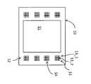
도 1(a) 및 도 1(b)는 복수의 접합 패드 어레이들을 갖는, CMOS 센서, 및 ASIC의 윗면의 모습을 도시한다.
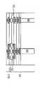
도 2(a) 및 도 2(b)는 CMOS 센서의 접합 패드 어레이 내의 접합 패드들을 연결하기 위한 방법 및 장치를 도시한다.
도 3(a) 내지 도 3(d)는 CMOS 센서의 접합 패드 어레이 내의 접합 패드들의 구성들을 위한 방법 및 장치를 도시한다.
도 4(a) 및 도 4(b)는 CMOS 센서의 접합 패드 어레이 내의 접합 패드들에 대한 평면도들을 도시한다.
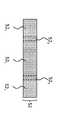
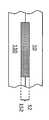
도 5는 CMOS 센서와 ASIC의 접합의 단면도를 도시한다.
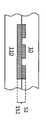
도 6(a) 내지 도 6(c)는 CMOS 센서의 접합 패드 어레이와 ASIC의 접합 패드 어레이의 접합의 단면도를 도시한다.
여러 도면들에서의 대응하는 숫자들 및 심볼들은 이와 다르게 언급되지 않는 한 일반적으로 대응하는 부분들을 가리킨다. 다양한 실시예들의 관련된 양태들을 명확하게 설명하기 위해 도면들이 도시되고 있으며, 도면들은 반드시 실척도로 도시되어 있지는 않다.
Claims (10)
- 후면 조명(backside illuminated; BSI) 센서 디바이스에 있어서,
전면부와 후면부를 갖는 기판;
상기 기판의 활성 영역 내의 감광성 다이오드; 및
상기 기판의 전면부에 있는 제1 접합 패드 어레이를 포함하며, 상기 제1 접합 패드 어레이는, 개구에 의해 서로 분리되어 있되 서로 전기적으로 연결되어 있으며 하나의 전기적 접촉부로서 기능을 하는 제1 접합 패드와 제2 접합 패드를 포함한 것인, 후면 조명(BSI) 센서 디바이스. - 제1항에 있어서, 상기 제1 접합 패드 어레이는, 서로가 전기적으로 연결되면서 상기 제1 접합 패드와 상기 제2 접합 패드에 전기적으로 모두 연결되는 추가적인 접합 패드들을 더 포함한 것인, 후면 조명(BSI) 센서 디바이스.
- 제1항에 있어서, 상기 감광성 다이오드는 p-n-p 접합을 포함한 핀(pinned)층 광다이오드인 것인, 후면 조명(BSI) 센서 디바이스.
- 제1항에 있어서, 상기 기판의 후면부상의 마이크로렌즈와 칼라 필터를 더 포함한, 후면 조명(BSI) 센서 디바이스.
- 제1항에 있어서, 상기 제1 접합 패드 어레이의 상기 제1 접합 패드와 상기 제2 접합 패드는 상기 제1 접합 패드와 상기 제2 접합 패드가 형성되어 있는 동일한 층에서 전기적으로 상호연결되는 것인, 후면 조명(BSI) 센서 디바이스.
- 제1항에 있어서, 상기 제1 접합 패드와 상기 제2 접합 패드는 개별적으로 존재하며, 상기 제1 접합 패드 및 상기 제2 접합 패드와는 상이한 층에 있는 상호연결부는 상기 제1 접합 패드와 상기 제2 접합 패드를 전기적으로 상호연결시키는 것인, 후면 조명(BSI) 센서 디바이스.
- 제1항에 있어서, 상기 제1 접합 패드 어레이에 연결된 쓰루 비아를 더 포함한, 후면 조명(BSI) 센서 디바이스.
- 제1항에 있어서, 상기 제1 접합 패드 어레이와 동일한 레벨에 있되 상기 제1 접합 패드 어레이로부터 전기적으로 연결해제되어 있는 고형(solid) 접합 패드를 더 포함하며, 상기 고형 접합 패드는 상기 제1 접합 패드 어레이보다 폭이 작은 것인, 후면 조명(BSI) 센서 디바이스.
- 제1항에 있어서,
기판, 및 상기 기판의 전면부에 있는 제2 접합 패드 어레이를 포함한 ASIC 칩을 더 포함하며, 상기 제2 접합 패드 어레이는, 서로 분리되어 있되 서로 전기적으로 연결되어 있으며 하나의 전기적 접촉부로서 기능을 하는 제3 접합 패드와 제4 접합 패드를 포함하며,
상기 제1 접합 패드 어레이의 상기 제1 접합 패드와 상기 제2 접합 패드 어레이의 상기 제3 접합 패드는 함께 접합되는 것인, 후면 조명(BSI) 센서 디바이스. - 집적 회로(integrated circuit; IC) 패키지에 있어서,
센서 디바이스와,
ASIC 칩을 포함하고,
상기 센서 디바이스는,
전면부와 후면부를 갖는 기판;
상기 기판의 활성 영역 내의 감광성 다이오드; 및
상기 기판의 전면부에 있는 제1 접합 패드 어레이를 포함하며, 상기 제1 접합 패드 어레이는, 개구에 의해 서로 분리되어 있되 서로 전기적으로 연결되어 있으며 하나의 전기적 접촉부로서 기능을 하는 제1 접합 패드와 제2 접합 패드를 포함하며,
상기 ASIC 칩은,
기판과,
상기 기판의 전면부에 있는 제2 접합 패드 어레이를 포함하고, 상기 제2 접합 패드 어레이는, 개구에 의해 서로 분리되어 있되 서로 전기적으로 연결되어 있으며 하나의 전기적 접촉부로서 기능을 하는 제3 접합 패드와 제4 접합 패드를 포함하며,
상기 제1 접합 패드 어레이의 상기 제1 접합 패드와 상기 제2 접합 패드 어레이의 상기 제3 접합 패드는 함께 접합되는 것인, 집적 회로(IC) 패키지.
Applications Claiming Priority (2)
| Application Number | Priority Date | Filing Date | Title |
|---|---|---|---|
| US13/547,269US8710607B2 (en) | 2012-07-12 | 2012-07-12 | Method and apparatus for image sensor packaging |
| US13/547,269 | 2012-07-12 |
Publications (1)
| Publication Number | Publication Date |
|---|---|
| KR20140008983Atrue KR20140008983A (ko) | 2014-01-22 |
Family
ID=49913277
Family Applications (1)
| Application Number | Title | Priority Date | Filing Date |
|---|---|---|---|
| KR1020120109897ACeasedKR20140008983A (ko) | 2012-07-12 | 2012-10-04 | 이미지 센서 패키징을 위한 방법 및 장치 |
Country Status (3)
| Country | Link |
|---|---|
| US (3) | US8710607B2 (ko) |
| KR (1) | KR20140008983A (ko) |
| CN (1) | CN103545324B (ko) |
Cited By (8)
| Publication number | Priority date | Publication date | Assignee | Title |
|---|---|---|---|---|
| KR20180097522A (ko)* | 2015-12-21 | 2018-08-31 | 소니 주식회사 | 고체 촬상 소자 및 전자 장치 |
| KR20190058345A (ko)* | 2017-11-21 | 2019-05-29 | 타이완 세미콘덕터 매뉴팩쳐링 컴퍼니 리미티드 | 균일한 웨이퍼 평탄화 및 접합을 위한 앵커 구조물 및 방법 |
| KR20190064500A (ko)* | 2017-11-30 | 2019-06-10 | 타이완 세미콘덕터 매뉴팩쳐링 컴퍼니 리미티드 | 반도체 디바이스 및 그 제조 방법 |
| KR20200002698A (ko)* | 2018-06-29 | 2020-01-08 | 타이완 세미콘덕터 매뉴팩쳐링 컴퍼니 리미티드 | 반도체 상호접속 구조물 및 방법 |
| US10672820B2 (en) | 2017-11-23 | 2020-06-02 | Taiwan Semiconductor Manufacturing Co., Ltd. | Hybrid bonded structure |
| KR20200093195A (ko)* | 2019-01-28 | 2020-08-05 | 삼성전자주식회사 | 접합 패드를 갖는 반도체 소자 |
| US10879293B2 (en) | 2016-12-20 | 2020-12-29 | Sony Semiconductor Solutions Corporation | Solid-state imaging device, method of manufacturing solid-state imaging device, and electronic device |
| US11817472B2 (en) | 2017-11-21 | 2023-11-14 | Taiwan Semiconductor Manufacturing Co., Ltd. | Anchor structures and methods for uniform wafer planarization and bonding |
Families Citing this family (14)
| Publication number | Priority date | Publication date | Assignee | Title |
|---|---|---|---|---|
| TWI676279B (zh)* | 2013-10-04 | 2019-11-01 | 新力股份有限公司 | 半導體裝置及固體攝像元件 |
| US9679936B2 (en) | 2014-02-27 | 2017-06-13 | Semiconductor Components Industries, Llc | Imaging systems with through-oxide via connections |
| TWI692859B (zh)* | 2015-05-15 | 2020-05-01 | 日商新力股份有限公司 | 固體攝像裝置及其製造方法、以及電子機器 |
| JP6856983B2 (ja)* | 2016-06-30 | 2021-04-14 | キヤノン株式会社 | 光電変換装置及びカメラ |
| KR102051373B1 (ko)* | 2016-09-23 | 2019-12-04 | 삼성전자주식회사 | 팬-아웃 센서 패키지 및 이를 포함하는 카메라 모듈 |
| US10178764B2 (en)* | 2017-06-05 | 2019-01-08 | Waymo Llc | PCB optical isolation by nonuniform catch pad stack |
| DE102018125106B4 (de) | 2017-11-23 | 2023-10-05 | Taiwan Semiconductor Manufacturing Co., Ltd. | Hybridgebondete Struktur und Verfahren zu deren Herstellung |
| EP3525232A1 (en)* | 2018-02-09 | 2019-08-14 | Nexperia B.V. | Semiconductor device and method of manufacturing the same |
| CN112292757B (zh)* | 2018-08-24 | 2024-03-05 | 铠侠股份有限公司 | 半导体装置及其制造方法 |
| CN110112097A (zh)* | 2019-05-21 | 2019-08-09 | 德淮半导体有限公司 | 晶圆键合结构以及晶圆键合结构的制作方法 |
| CN110391147A (zh)* | 2019-07-26 | 2019-10-29 | 德淮半导体有限公司 | 衬垫结构及其形成方法 |
| KR20220033619A (ko) | 2020-09-08 | 2022-03-17 | 삼성전자주식회사 | 반도체 패키지 |
| CN113629087B (zh)* | 2021-08-06 | 2023-12-22 | 武汉新芯集成电路制造有限公司 | Bsi图像传感器装置及制作方法 |
| CN115910825A (zh)* | 2022-11-15 | 2023-04-04 | 上海华力微电子有限公司 | 焊盘结构及光刻拼接工艺的在线监控方法 |
Family Cites Families (26)
| Publication number | Priority date | Publication date | Assignee | Title |
|---|---|---|---|---|
| US6020629A (en)* | 1998-06-05 | 2000-02-01 | Micron Technology, Inc. | Stacked semiconductor package and method of fabrication |
| US8021976B2 (en)* | 2002-10-15 | 2011-09-20 | Megica Corporation | Method of wire bonding over active area of a semiconductor circuit |
| US7189595B2 (en)* | 2001-05-31 | 2007-03-13 | International Business Machines Corporation | Method of manufacture of silicon based package and devices manufactured thereby |
| US6510195B1 (en)* | 2001-07-18 | 2003-01-21 | Koninklijke Philips Electronics, N.V. | Solid state x-radiation detector modules and mosaics thereof, and an imaging method and apparatus employing the same |
| US7282382B2 (en)* | 2001-10-29 | 2007-10-16 | Stmicroelectronics N.V. | Method for producing a photodiode contact for a TFA image sensor |
| JP3778445B2 (ja)* | 2003-03-27 | 2006-05-24 | 富士通株式会社 | 半導体装置 |
| US20060001180A1 (en)* | 2004-06-30 | 2006-01-05 | Brian Taggart | In-line wire bonding on a package, and method of assembling same |
| US7973380B2 (en)* | 2005-11-23 | 2011-07-05 | Taiwan Semiconductor Manufacturing Company, Ltd. | Method for providing metal extension in backside illuminated sensor for wafer level testing |
| KR100801447B1 (ko)* | 2006-06-19 | 2008-02-11 | (주)실리콘화일 | 배면 광 포토다이오드를 이용한 이미지센서 및 그 제조방법 |
| US7622364B2 (en)* | 2006-08-18 | 2009-11-24 | International Business Machines Corporation | Bond pad for wafer and package for CMOS imager |
| US20080246152A1 (en)* | 2007-04-04 | 2008-10-09 | Taiwan Semiconductor Manufacturing Co., Ltd. | Semiconductor device with bonding pad |
| JP4609497B2 (ja)* | 2008-01-21 | 2011-01-12 | ソニー株式会社 | 固体撮像装置とその製造方法、及びカメラ |
| US7982177B2 (en)* | 2008-01-31 | 2011-07-19 | Omnivision Technologies, Inc. | Frontside illuminated image sensor comprising a complex-shaped reflector |
| US8101978B2 (en)* | 2008-02-08 | 2012-01-24 | Omnivision Technologies, Inc. | Circuit and photo sensor overlap for backside illumination image sensor |
| US7859033B2 (en)* | 2008-07-09 | 2010-12-28 | Eastman Kodak Company | Wafer level processing for backside illuminated sensors |
| US7973310B2 (en) | 2008-07-11 | 2011-07-05 | Chipmos Technologies Inc. | Semiconductor package structure and method for manufacturing the same |
| US9041841B2 (en)* | 2008-10-10 | 2015-05-26 | Taiwan Semiconductor Manufacturing Company, Ltd. | Image sensor having enhanced backside illumination quantum efficiency |
| US8053900B2 (en) | 2008-10-21 | 2011-11-08 | Taiwan Semiconductor Manufacturing Company, Ltd. | Through-substrate vias (TSVs) electrically connected to a bond pad design with reduced dishing effect |
| US8125042B2 (en)* | 2008-11-13 | 2012-02-28 | Samsung Electronics Co., Ltd. | Semiconductor package and method of manufacturing the same |
| US9142586B2 (en)* | 2009-02-24 | 2015-09-22 | Taiwan Semiconductor Manufacturing Company, Ltd. | Pad design for backside illuminated image sensor |
| JP5985136B2 (ja) | 2009-03-19 | 2016-09-06 | ソニー株式会社 | 半導体装置とその製造方法、及び電子機器 |
| TWI420662B (zh)* | 2009-12-25 | 2013-12-21 | Sony Corp | 半導體元件及其製造方法,及電子裝置 |
| JP5685898B2 (ja)* | 2010-01-08 | 2015-03-18 | ソニー株式会社 | 半導体装置、固体撮像装置、およびカメラシステム |
| US8431977B2 (en)* | 2010-06-10 | 2013-04-30 | Megica Corporation | Wafer level processing method and structure to manufacture semiconductor chip |
| JP2012079979A (ja)* | 2010-10-04 | 2012-04-19 | Sony Corp | 固体撮像装置、および、その製造方法、電子機器 |
| US8604576B2 (en)* | 2011-07-19 | 2013-12-10 | Opitz, Inc. | Low stress cavity package for back side illuminated image sensor, and method of making same |
- 2012
- 2012-07-12USUS13/547,269patent/US8710607B2/enactiveActive
- 2012-10-04KRKR1020120109897Apatent/KR20140008983A/konot_activeCeased
- 2012-10-25CNCN201210414021.9Apatent/CN103545324B/zhactiveActive
- 2014
- 2014-03-11USUS14/204,921patent/US9029183B2/enactiveActive
- 2015
- 2015-05-01USUS14/702,450patent/US9917123B2/enactiveActive
Cited By (12)
| Publication number | Priority date | Publication date | Assignee | Title |
|---|---|---|---|---|
| KR20180097522A (ko)* | 2015-12-21 | 2018-08-31 | 소니 주식회사 | 고체 촬상 소자 및 전자 장치 |
| US10879293B2 (en) | 2016-12-20 | 2020-12-29 | Sony Semiconductor Solutions Corporation | Solid-state imaging device, method of manufacturing solid-state imaging device, and electronic device |
| KR20190058345A (ko)* | 2017-11-21 | 2019-05-29 | 타이완 세미콘덕터 매뉴팩쳐링 컴퍼니 리미티드 | 균일한 웨이퍼 평탄화 및 접합을 위한 앵커 구조물 및 방법 |
| US11152417B2 (en) | 2017-11-21 | 2021-10-19 | Taiwan Semiconductor Manufacturing Co., Ltd. | Anchor structures and methods for uniform wafer planarization and bonding |
| US11817472B2 (en) | 2017-11-21 | 2023-11-14 | Taiwan Semiconductor Manufacturing Co., Ltd. | Anchor structures and methods for uniform wafer planarization and bonding |
| US10672820B2 (en) | 2017-11-23 | 2020-06-02 | Taiwan Semiconductor Manufacturing Co., Ltd. | Hybrid bonded structure |
| KR20210066770A (ko)* | 2017-11-23 | 2021-06-07 | 타이완 세미콘덕터 매뉴팩쳐링 컴퍼니 리미티드 | 하이브리드 본딩된 구조물 |
| KR20190064500A (ko)* | 2017-11-30 | 2019-06-10 | 타이완 세미콘덕터 매뉴팩쳐링 컴퍼니 리미티드 | 반도체 디바이스 및 그 제조 방법 |
| KR20200002698A (ko)* | 2018-06-29 | 2020-01-08 | 타이완 세미콘덕터 매뉴팩쳐링 컴퍼니 리미티드 | 반도체 상호접속 구조물 및 방법 |
| US11424205B2 (en) | 2018-06-29 | 2022-08-23 | Taiwan Semiconductor Manufacturing Company, Ltd. | Semiconductor interconnect structure and method |
| US12154876B2 (en) | 2018-06-29 | 2024-11-26 | Taiwan Semiconductor Manufacturing Company, Ltd. | Semiconductor interconnect structure and method |
| KR20200093195A (ko)* | 2019-01-28 | 2020-08-05 | 삼성전자주식회사 | 접합 패드를 갖는 반도체 소자 |
Also Published As
| Publication number | Publication date |
|---|---|
| US9029183B2 (en) | 2015-05-12 |
| US8710607B2 (en) | 2014-04-29 |
| US20150236064A1 (en) | 2015-08-20 |
| US20140015084A1 (en) | 2014-01-16 |
| CN103545324B (zh) | 2016-12-21 |
| US9917123B2 (en) | 2018-03-13 |
| US20140193940A1 (en) | 2014-07-10 |
| CN103545324A (zh) | 2014-01-29 |
Similar Documents
| Publication | Publication Date | Title |
|---|---|---|
| US9029183B2 (en) | Method and apparatus for image sensor packaging | |
| US10096645B2 (en) | Method and apparatus for image sensor packaging | |
| US10930699B2 (en) | Method and apparatus for image sensor packaging | |
| JP5843475B2 (ja) | 固体撮像装置および固体撮像装置の製造方法 | |
| US9087760B2 (en) | Semiconductor device and method of manufacturing the same, and electronic apparatus | |
| US9006807B2 (en) | Solid-state image sensing device and camera | |
| JP5532867B2 (ja) | 固体撮像装置及びその製造方法、並びに固体撮像素子の製造方法及び半導体装置 | |
| US20100237452A1 (en) | Semiconductor device and backside illumination solid-state imaging device | |
| US9324744B2 (en) | Solid-state image sensor having a trench and method of manufacturing the same | |
| CN101005090A (zh) | 背照式影像感测元件、其形成方法及封装 | |
| TWI389330B (zh) | 背側照明成像器以及製造其之方法 | |
| US8895936B2 (en) | Pixel array and image sensor including the same | |
| JP2019195082A (ja) | 固体撮像装置および固体撮像装置の製造方法 | |
| CN107425026A (zh) | 半导体器件及其制造方法 | |
| KR20250083403A (ko) | 조합된 단파장 적외선 및 가시광선 센서, 이를 포함하는 이미저 및 이를 제조하는 방법 | |
| CN120344010A (zh) | 图像传感器 |
Legal Events
| Date | Code | Title | Description |
|---|---|---|---|
| A201 | Request for examination | ||
| PA0109 | Patent application | Patent event code:PA01091R01D Comment text:Patent Application Patent event date:20121004 | |
| PA0201 | Request for examination | ||
| E902 | Notification of reason for refusal | ||
| PE0902 | Notice of grounds for rejection | Comment text:Notification of reason for refusal Patent event date:20130923 Patent event code:PE09021S01D | |
| AMND | Amendment | ||
| PG1501 | Laying open of application | ||
| E601 | Decision to refuse application | ||
| PE0601 | Decision on rejection of patent | Patent event date:20140528 Comment text:Decision to Refuse Application Patent event code:PE06012S01D Patent event date:20130923 Comment text:Notification of reason for refusal Patent event code:PE06011S01I | |
| AMND | Amendment | ||
| PX0901 | Re-examination | Patent event code:PX09011S01I Patent event date:20140528 Comment text:Decision to Refuse Application Patent event code:PX09012R01I Patent event date:20131223 Comment text:Amendment to Specification, etc. | |
| PX0601 | Decision of rejection after re-examination | Comment text:Decision to Refuse Application Patent event code:PX06014S01D Patent event date:20140811 Comment text:Amendment to Specification, etc. Patent event code:PX06012R01I Patent event date:20140630 Comment text:Decision to Refuse Application Patent event code:PX06011S01I Patent event date:20140528 Comment text:Amendment to Specification, etc. Patent event code:PX06012R01I Patent event date:20131223 Comment text:Notification of reason for refusal Patent event code:PX06013S01I Patent event date:20130923 | |
| J201 | Request for trial against refusal decision | ||
| PJ0201 | Trial against decision of rejection | Patent event date:20141111 Comment text:Request for Trial against Decision on Refusal Patent event code:PJ02012R01D Patent event date:20140811 Comment text:Decision to Refuse Application Patent event code:PJ02011S01I Patent event date:20140528 Comment text:Decision to Refuse Application Patent event code:PJ02011S01I Appeal kind category:Appeal against decision to decline refusal Appeal identifier:2014101006983 Request date:20141111 | |
| J301 | Trial decision | Free format text:TRIAL DECISION FOR APPEAL AGAINST DECISION TO DECLINE REFUSAL REQUESTED 20141111 Effective date:20160122 | |
| PJ1301 | Trial decision | Patent event code:PJ13011S01D Patent event date:20160122 Comment text:Trial Decision on Objection to Decision on Refusal Appeal kind category:Appeal against decision to decline refusal Request date:20141111 Decision date:20160122 Appeal identifier:2014101006983 |