KR20140008983A - Method and apparatus for image sensor packaging - Google Patents
Method and apparatus for image sensor packagingDownload PDFInfo
- Publication number
- KR20140008983A KR20140008983AKR1020120109897AKR20120109897AKR20140008983AKR 20140008983 AKR20140008983 AKR 20140008983AKR 1020120109897 AKR1020120109897 AKR 1020120109897AKR 20120109897 AKR20120109897 AKR 20120109897AKR 20140008983 AKR20140008983 AKR 20140008983A
- Authority
- KR
- South Korea
- Prior art keywords
- bond pad
- array
- bond
- substrate
- pad array
- Prior art date
- Legal status (The legal status is an assumption and is not a legal conclusion. Google has not performed a legal analysis and makes no representation as to the accuracy of the status listed.)
- Ceased
Links
Images


Classifications
- H—ELECTRICITY
- H10—SEMICONDUCTOR DEVICES; ELECTRIC SOLID-STATE DEVICES NOT OTHERWISE PROVIDED FOR
- H10F—INORGANIC SEMICONDUCTOR DEVICES SENSITIVE TO INFRARED RADIATION, LIGHT, ELECTROMAGNETIC RADIATION OF SHORTER WAVELENGTH OR CORPUSCULAR RADIATION
- H10F39/00—Integrated devices, or assemblies of multiple devices, comprising at least one element covered by group H10F30/00, e.g. radiation detectors comprising photodiode arrays
- H10F39/10—Integrated devices
- H10F39/12—Image sensors
- H—ELECTRICITY
- H10—SEMICONDUCTOR DEVICES; ELECTRIC SOLID-STATE DEVICES NOT OTHERWISE PROVIDED FOR
- H10F—INORGANIC SEMICONDUCTOR DEVICES SENSITIVE TO INFRARED RADIATION, LIGHT, ELECTROMAGNETIC RADIATION OF SHORTER WAVELENGTH OR CORPUSCULAR RADIATION
- H10F39/00—Integrated devices, or assemblies of multiple devices, comprising at least one element covered by group H10F30/00, e.g. radiation detectors comprising photodiode arrays
- H10F39/80—Constructional details of image sensors
- H10F39/811—Interconnections
- H—ELECTRICITY
- H01—ELECTRIC ELEMENTS
- H01L—SEMICONDUCTOR DEVICES NOT COVERED BY CLASS H10
- H01L24/00—Arrangements for connecting or disconnecting semiconductor or solid-state bodies; Methods or apparatus related thereto
- H01L24/01—Means for bonding being attached to, or being formed on, the surface to be connected, e.g. chip-to-package, die-attach, "first-level" interconnects; Manufacturing methods related thereto
- H01L24/02—Bonding areas ; Manufacturing methods related thereto
- H01L24/04—Structure, shape, material or disposition of the bonding areas prior to the connecting process
- H01L24/06—Structure, shape, material or disposition of the bonding areas prior to the connecting process of a plurality of bonding areas
- H—ELECTRICITY
- H10—SEMICONDUCTOR DEVICES; ELECTRIC SOLID-STATE DEVICES NOT OTHERWISE PROVIDED FOR
- H10F—INORGANIC SEMICONDUCTOR DEVICES SENSITIVE TO INFRARED RADIATION, LIGHT, ELECTROMAGNETIC RADIATION OF SHORTER WAVELENGTH OR CORPUSCULAR RADIATION
- H10F39/00—Integrated devices, or assemblies of multiple devices, comprising at least one element covered by group H10F30/00, e.g. radiation detectors comprising photodiode arrays
- H10F39/10—Integrated devices
- H10F39/12—Image sensors
- H10F39/199—Back-illuminated image sensors
- H—ELECTRICITY
- H10—SEMICONDUCTOR DEVICES; ELECTRIC SOLID-STATE DEVICES NOT OTHERWISE PROVIDED FOR
- H10F—INORGANIC SEMICONDUCTOR DEVICES SENSITIVE TO INFRARED RADIATION, LIGHT, ELECTROMAGNETIC RADIATION OF SHORTER WAVELENGTH OR CORPUSCULAR RADIATION
- H10F39/00—Integrated devices, or assemblies of multiple devices, comprising at least one element covered by group H10F30/00, e.g. radiation detectors comprising photodiode arrays
- H10F39/80—Constructional details of image sensors
- H10F39/805—Coatings
- H10F39/8053—Colour filters
- H—ELECTRICITY
- H10—SEMICONDUCTOR DEVICES; ELECTRIC SOLID-STATE DEVICES NOT OTHERWISE PROVIDED FOR
- H10F—INORGANIC SEMICONDUCTOR DEVICES SENSITIVE TO INFRARED RADIATION, LIGHT, ELECTROMAGNETIC RADIATION OF SHORTER WAVELENGTH OR CORPUSCULAR RADIATION
- H10F39/00—Integrated devices, or assemblies of multiple devices, comprising at least one element covered by group H10F30/00, e.g. radiation detectors comprising photodiode arrays
- H10F39/80—Constructional details of image sensors
- H10F39/806—Optical elements or arrangements associated with the image sensors
- H10F39/8063—Microlenses
- H—ELECTRICITY
- H10—SEMICONDUCTOR DEVICES; ELECTRIC SOLID-STATE DEVICES NOT OTHERWISE PROVIDED FOR
- H10F—INORGANIC SEMICONDUCTOR DEVICES SENSITIVE TO INFRARED RADIATION, LIGHT, ELECTROMAGNETIC RADIATION OF SHORTER WAVELENGTH OR CORPUSCULAR RADIATION
- H10F39/00—Integrated devices, or assemblies of multiple devices, comprising at least one element covered by group H10F30/00, e.g. radiation detectors comprising photodiode arrays
- H10F39/80—Constructional details of image sensors
- H10F39/809—Constructional details of image sensors of hybrid image sensors
- H—ELECTRICITY
- H10—SEMICONDUCTOR DEVICES; ELECTRIC SOLID-STATE DEVICES NOT OTHERWISE PROVIDED FOR
- H10F—INORGANIC SEMICONDUCTOR DEVICES SENSITIVE TO INFRARED RADIATION, LIGHT, ELECTROMAGNETIC RADIATION OF SHORTER WAVELENGTH OR CORPUSCULAR RADIATION
- H10F99/00—Subject matter not provided for in other groups of this subclass
- H—ELECTRICITY
- H01—ELECTRIC ELEMENTS
- H01L—SEMICONDUCTOR DEVICES NOT COVERED BY CLASS H10
- H01L2224/00—Indexing scheme for arrangements for connecting or disconnecting semiconductor or solid-state bodies and methods related thereto as covered by H01L24/00
- H01L2224/01—Means for bonding being attached to, or being formed on, the surface to be connected, e.g. chip-to-package, die-attach, "first-level" interconnects; Manufacturing methods related thereto
- H01L2224/02—Bonding areas; Manufacturing methods related thereto
- H01L2224/04—Structure, shape, material or disposition of the bonding areas prior to the connecting process
- H01L2224/06—Structure, shape, material or disposition of the bonding areas prior to the connecting process of a plurality of bonding areas
- H01L2224/0601—Structure
- H01L2224/0603—Bonding areas having different sizes, e.g. different heights or widths
- H—ELECTRICITY
- H01—ELECTRIC ELEMENTS
- H01L—SEMICONDUCTOR DEVICES NOT COVERED BY CLASS H10
- H01L2224/00—Indexing scheme for arrangements for connecting or disconnecting semiconductor or solid-state bodies and methods related thereto as covered by H01L24/00
- H01L2224/01—Means for bonding being attached to, or being formed on, the surface to be connected, e.g. chip-to-package, die-attach, "first-level" interconnects; Manufacturing methods related thereto
- H01L2224/02—Bonding areas; Manufacturing methods related thereto
- H01L2224/04—Structure, shape, material or disposition of the bonding areas prior to the connecting process
- H01L2224/06—Structure, shape, material or disposition of the bonding areas prior to the connecting process of a plurality of bonding areas
- H01L2224/061—Disposition
- H01L2224/0612—Layout
- H01L2224/0613—Square or rectangular array
- H01L2224/06131—Square or rectangular array being uniform, i.e. having a uniform pitch across the array
- H—ELECTRICITY
- H01—ELECTRIC ELEMENTS
- H01L—SEMICONDUCTOR DEVICES NOT COVERED BY CLASS H10
- H01L2924/00—Indexing scheme for arrangements or methods for connecting or disconnecting semiconductor or solid-state bodies as covered by H01L24/00
- H01L2924/10—Details of semiconductor or other solid state devices to be connected
- H01L2924/11—Device type
- H01L2924/12—Passive devices, e.g. 2 terminal devices
- H01L2924/1204—Optical Diode
- H01L2924/12043—Photo diode
Landscapes
- Engineering & Computer Science (AREA)
- Computer Hardware Design (AREA)
- Microelectronics & Electronic Packaging (AREA)
- Power Engineering (AREA)
- Solid State Image Pick-Up Elements (AREA)
Abstract
Translated fromKorean
Description
Translated fromKorean본 개시내용은 응용 특정 집적 회로(ASIC)와 함께 후면 조명(backside illuminated; BSI) 이미지 센서 또는 BSI 센서 디바이스를 패키지화하기 위한 방법 및 장치를 개시한다.The present disclosure discloses a method and apparatus for packaging a backside illuminated (BSI) image sensor or BSI sensor device with an application specific integrated circuit (ASIC).
상보적 금속 산화물 반도체(complementary metal oxide semiconductor; CMOS) 이미지 센서들은 종래의 전하 결합 디바이스(charged-coupled device; CCD)에 비해 인기를 끌고 있다. 일반적으로 CMOS 이미지 센서는 광자를 전자로 변환시키기 위해 감광성 CMOS 회로를 이용하는 픽처 엘리먼트(픽셀)들의 어레이를 포함한다. 감광성 CMOS 회로는 일반적으로 실리콘 기판에서 형성된 광다이오드를 포함한다. 광다이오드가 광에 노출될 때, 광다이오드에서는 전하가 유도된다. 피사체 장면으로부터의 광이 픽셀상에 입사될 때 각각의 픽셀은 픽셀상에 낙하되는 광의 양에 비례하여 전자들을 생성시킬 수 있다. 전자들은 픽셀내에서 전압 신호로 변환되고 더 나아가 디지털 신호로 전환되어 응용 특정 집적 회로(application specific integrated circuit (ASIC)에 의해 처리될 것이다.Complementary metal oxide semiconductor (CMOS) image sensors are becoming more popular than conventional charge-coupled devices (CCDs). Generally, a CMOS image sensor includes an array of picture elements (pixels) that use photosensitive CMOS circuits to convert photons to electrons. A photosensitive CMOS circuit generally comprises a photodiode formed on a silicon substrate. When the photodiode is exposed to light, charge is induced in the photodiode. When light from a subject scene is incident on a pixel, each pixel can produce electrons proportional to the amount of light falling on the pixel. The electrons are converted into a voltage signal in the pixel and further converted into a digital signal to be processed by an application specific integrated circuit (ASIC).
CMOS 이미지 센서, 또는 간략히 CMOS 센서는 기판에 있는 광다이오드를 주변 회로에 연결시켜주는 복수의 유전체층들 및 상호접속층들이 위치해 있는 전면부와, 기판을 구비한 후면부를 가질 수 있다. 광이 CMOS 센서의 전면부로부터 유입되면 CMOS 센서는 전면 조명(front-side illuminated; FSI) 이미지 센서이고, 그렇지 않은 경우에는 광이 후면상에 입사하는 후면 조명(back-side illuminated; BSI) 센서이다. BSI 센서의 경우, 광은 전면부에 위치한 유전체층들 및 상호연결층들로부터의 막힘없이 직접적 경로를 통해 광다이오드에 부딪칠 수 있다. 이것은 전자로 변환되는 광자들의 갯수를 증가시키는데 도움을 주며, CMOS 센서가 광원에 보다 민감하게 만든다.A CMOS image sensor, or briefly a CMOS sensor, may have a front surface where a plurality of dielectric layers and interconnect layers are located and a back surface with a substrate, which connects the photodiodes in the substrate to the peripheral circuitry. If light comes from the front of the CMOS sensor, the CMOS sensor is a front-side illuminated (FSI) image sensor, otherwise it is a back-side illuminated (BSI) sensor with light incident on the back side. . In the case of a BSI sensor, light can strike the photodiode via a direct path without blockage from the dielectric layers and interconnect layers located at the front. This helps to increase the number of photons that are converted to electrons, making the CMOS sensor more sensitive to light sources.
이미지 센서 애플리케이션과 같은 현재의 애플리케이션들을 위해 필요한 고밀도를 달성하기 위해 삼차원(3D) 집적 회로(IC)가 이용될 수 있다. CMOS 센서가 3D IC내에서 패키지화되는 경우, CMOS 센서 및 이와 관련된 ASIC은 캐리어 웨이퍼에 병렬로 접합될 수 있는데, 이것은 캐리어 웨이퍼에 대해 보다 큰 면적을 차지할 수 있다. 그러므로, 관련된 ASIC에 접합된 CMOS 센서들을 위한 패키지 면적을 감소시키기 위한 방법 및 시스템이 필요하다.Dimensional (3D) integrated circuits (ICs) can be used to achieve the high density required for current applications such as image sensor applications. When a CMOS sensor is packaged in a 3D IC, the CMOS sensor and its associated ASIC can be bonded in parallel to the carrier wafer, which can occupy a larger area for the carrier wafer. Therefore, a need exists for a method and system for reducing the package area for CMOS sensors coupled to an associated ASIC.
실시예에 따르면, 접합 패드 어레이는 BSI 센서에서 형성될 수 있고, 접합 패드 어레이는 전기적으로 상호연결된 복수의 접합 패드들을 포함하며, 접합 패드 어레이의 각각의 접합 패드는 커다란 접합 패드의 디싱 효과(dishing effect)를 감소시킬 수 있도록 작은 크기를 갖는다. 접합 패드 어레이의 복수의 접합 패드들은 동일한 패드층 또는 상이한 금속층에서 상호연결될 수 있다. BSI 센서는 접합 패드 어레이들이 함께 정렬되고 접합되도록 ASIC에 대면(face-to-face) 방식으로 접합될 수 있다. According to an embodiment, the bond pad array can be formed in a BSI sensor, the bond pad array comprising a plurality of electrically interconnected bond pads, each bond pad of the bond pad array being dished out of a large bond pad. Small size to reduce the effect. The plurality of bond pads of the bond pad array may be interconnected in the same pad layer or different metal layers. The BSI sensor can be bonded in a face-to-face manner to the ASIC such that the bond pad arrays are aligned and bonded together.
본 개시내용의 실시예들을 채용함으로써, 접합 패드 어레이들은 디싱 효과가 발생할 염려없이 형성될 수 있고, 이에 따라 결과적인 접합은 보다 신뢰적일 수 있고, 보다 큰 전류들을 도통시킬 수 있다.By employing embodiments of the present disclosure, bond pad arrays can be formed without fear of dishing effects, so that the resulting junction can be more reliable and can conduct larger currents.
본 개시내용과, 본 개시내용의 장점들의 보다 완벽한 이해를 위해, 이제부터 첨부 도면들을 참조하면서 이하의 상세한 설명에 대해 설명을 한다.
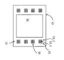
도 1(a) 및 도 1(b)는 복수의 접합 패드 어레이들을 갖는, CMOS 센서, 및 ASIC의 윗면의 모습을 도시한다.
도 2(a) 및 도 2(b)는 CMOS 센서의 접합 패드 어레이 내의 접합 패드들을 연결하기 위한 방법 및 장치를 도시한다.
도 3(a) 내지 도 3(d)는 CMOS 센서의 접합 패드 어레이 내의 접합 패드들의 구성들을 위한 방법 및 장치를 도시한다.
도 4(a) 및 도 4(b)는 CMOS 센서의 접합 패드 어레이 내의 접합 패드들에 대한 평면도들을 도시한다.
도 5는 CMOS 센서와 ASIC의 접합의 단면도를 도시한다.
도 6(a) 내지 도 6(c)는 CMOS 센서의 접합 패드 어레이와 ASIC의 접합 패드 어레이의 접합의 단면도를 도시한다.
여러 도면들에서의 대응하는 숫자들 및 심볼들은 이와 다르게 언급되지 않는 한 일반적으로 대응하는 부분들을 가리킨다. 다양한 실시예들의 관련된 양태들을 명확하게 설명하기 위해 도면들이 도시되고 있으며, 도면들은 반드시 실척도로 도시되어 있지는 않다.DETAILED DESCRIPTION For a more complete understanding of the present disclosure and the advantages of the present disclosure, the following detailed description will now be described with reference to the accompanying drawings.
1 (a) and 1 (b) show a top view of a CMOS sensor, and an ASIC, having a plurality of junction pad arrays.
2 (a) and 2 (b) illustrate a method and apparatus for connecting bond pads in a bond pad array of a CMOS sensor.
3A-3D show a method and apparatus for configurations of bond pads in a bond pad array of a CMOS sensor.
4 (a) and 4 (b) show plan views of bond pads in a bond pad array of a CMOS sensor.
5 shows a cross-sectional view of the junction of a CMOS sensor and an ASIC.
6 (a) to 6 (c) show cross-sectional views of the bonding between the bonding pad array of the CMOS sensor and the bonding pad array of the ASIC.
Corresponding numbers and symbols in the various figures generally refer to corresponding parts unless otherwise indicated. The drawings are shown to clearly illustrate the relevant aspects of the various embodiments, and the drawings are not necessarily drawn to scale.
이하에서는 본 실시예들의 실시 및 이용을 자세하게 설명한다. 그러나, 본 개시내용은 폭넓게 다양한 특정 환경들에서 구체화될 수 있는 많은 적용가능한 발명적 개념들을 제공한다는 것을 알아야 한다. 설명하는 특정한 실시예들은 본 개시내용의 실시예들을 실시하고 이용하는 특정한 방법들에 대한 단순한 예시에 불과하며, 본 개시내용의 범위를 한정시키려는 것은 아니다.Hereinafter, implementation and use of the embodiments will be described in detail. However, it should be understood that the present disclosure provides many applicable inventive concepts that can be embodied in a wide variety of specific environments. The particular embodiments described are merely illustrative of specific ways of practicing and using the embodiments of the present disclosure, and are not intended to limit the scope of the present disclosure.
본 개시내용은 응용 특정 집적 회로(ASIC)와 함께 후면 조명(backside illuminated; BSI) 이미지 센서 또는 BSI 센서 디바이스를 패키지화하기 위한 방법 및 장치를 개시한다. 실시예에 따르면, 접합 패드 어레이는 BSI 센서에서 형성될 수 있고, 접합 패드 어레이는 전기적으로 상호연결된 복수의 접합 패드들을 포함하며, 접합 패드 어레이의 각각의 접합 패드는 커다란 접합 패드의 디싱 효과(dishing effect)를 감소시킬 수 있도록 작은 크기를 갖는다. 접합 패드 어레이의 복수의 접합 패드들은 동일한 패드층 또는 상이한 금속층에서 상호연결될 수 있다. BSI 센서는 접합 패드 어레이들이 함께 정렬되고 접합되도록 ASIC에 대면(face-to-face) 방식으로 접합될 수 있다.The present disclosure discloses a method and apparatus for packaging a backside illuminated (BSI) image sensor or BSI sensor device with an application specific integrated circuit (ASIC). According to an embodiment, the bond pad array can be formed in a BSI sensor, the bond pad array comprising a plurality of electrically interconnected bond pads, each bond pad of the bond pad array being dished out of a large bond pad. Small size to reduce the effect. The plurality of bond pads of the bond pad array may be interconnected in the same pad layer or different metal layers. The BSI sensor can be bonded in a face-to-face manner to the ASIC such that the bond pad arrays are aligned and bonded together.
도 1(a)는 CMOS 센서(10), 또는 센서(10)의 윗면의 표면 모습을 도시한다. 센서(10)는 능동 디바이스들 및 수동 디바이스들과 같은 수 많은 컴포넌트들로 구성될 수 있다. 센서는 도면부호 13과 14와 같은 복수의 접합 패드 어레이들이 위치하는 접합 패드 영역(12)과 활성 영역(11)을 포함할 수 있다. 몇몇의 다른 형태들의 접합 패드들이 또한 접합 패드 영역(12)에서 존재할 수 있다. 다수의 고밀도의, CMOS 센서(10)의 능동 회로들을 포함한 활성 영역(11)은 센서(10)의 비교적 중심 영역에 위치할 수 있다.FIG. 1A shows the surface of the
도면부호 13 및 14와 같은 복수의 접합 패드 어레이들은 CMOS 센서(10)의 주변부를 따라 위치한다. 접합 패드 어레이(13 또는 14)는 복수의 접합 패드들을 포함할 수 있다. 도 1(a)에서 도시된 바와 같이, 접합 패드 어레이(13)는 서로 분리되어 있는 제1 접합 패드(13_1)와 제2 접합 패드(13_2)를 포함한, 3*3 매트릭스 포맷으로서 배열된 총 아홉 개의 접합 패드들을 포함한다. 접합 패드(13_1)와 접합 패드(13_2)는 서로 전기적으로 함께 연결되어 있으며, 또한 접합 패드 어레이(13) 내의 나머지 다른 접합 패드들과도 서로 전기적으로 함께 연결되어 있다. 접합 패드 어레이(13) 내의 접합 패드들간의 상호연결은 윗면 아래의 금속층에서와 같이 다양한 방식으로 이루어질 수 있다. 접합 패드 어레이(13)는 또한 동일한 접합 어레이 내의 접합 패드들간의 거리와 비교하여 보다 큰 거리를 두면서 다른 접합 패드 어레이(14)로부터 분리되어 있다. 접합 패드 어레이(14) 내의 접합 패드들은 전기적으로 함께 연결되어 있지만, 접합 패드 어레이(13) 내의 접합 패드들과는 전기적으로 격리된다. 접합 패드 어레이(13)의 갯수 및 접합 패드 어레이 내의 접합 패드들의 갯수는 단시 예시용에 불과하며 이것으로 제한되는 것은 아니다. 다른 갯수의 접합 패드 어레이들이 존재할 수 있으며, 여기서 각각의 접합 패드 어레이는 상이한 갯수의 접합 패드들을 포함할 수 있다.A plurality of bond pad arrays, such as
마찬가지로, 응용 특정 집적 회로(ASIC)(110)의 윗면도가 도 1(b)에서 도시된다. ASIC(110)은 센서(10)에 의해 생성된 디지털 또는 아날로그 신호들을 처리하기 위해 센서(10)와 연계될 수 있다. ASIC(110)는 능동 디바이스들 및 수동 디바이스들과 같은 수 많은 컴포넌트들로 구성될 수 있다. 이들 컴포넌트들은 초기에 서로 격리된 상태로, 아래에 위치한 실리콘 기판상에 형성되며, 그런 후 금속 상호연결배선들에 의해 함께 상호연결되어 기능 회로를 형성한다. 통상의 상호연결 구조물들은 금속선 또는 와이어와 같은 횡측 상호연결부와, 비아 및 컨택트와 같은 수직적 상호연결부를 포함한다. 집적 회로가 형성되어 있는 실리콘 기판의 측면을 ASIC(110)의 윗면 또는 전면부라고 칭할 수 있다. ASIC(110)은 집적 회로 디바이스, 회로, 디바이스, 회로 디바이스, 다이, 또는 본 업계에 있는 당업자에게 알려진 임의의 다른 용어들로 칭해질 수 있다.Similarly, a top view of an application specific integrated circuit (ASIC) 110 is shown in FIG. 1 (b). ASIC 110 may be associated with
도 1(b)에서 도시된 바와 같이, 접합 패드 어레이(113)와 접합 패드 어레이(114)는 접합 패드 영역(112) 내에서 ASIC(110)의 주변부를 따라 위치한다. 집적 회로 디바이스(110)의 중심부에는 다수의 고밀도의, ASIC(110)의 능동 회로들을 포함한 활성 영역(111)이 있다. ASIC(110)는 또한 접합 패드 어레이(113)의 외부에 위치하여 ASIC(110)를 보호해주는 가드 링 영역(미도시됨)에 의해 둘러싸여질 수 있다.As shown in FIG. 1B, the
도 1(a)에서의 접합 패드 어레이(13)와 도 1(b)에서의 접합 패드 어레이(113)는 데이터를 공급하고, 데이터를 인출하고, 디바이스를 테스트하며, 테스트 또는 프로그래밍을 위한 다양한 전압들을 공급하는 기능을 할 수 있다. 예시적인 접합 패드 어레이는 동작 모드 접합 패드 어레이로부터 분리되어 있고 이에 연결되어 있지 않은 테스트 모드 접합 패드 어레이를 포함한다. 테스트 시퀀스가 완료되면, 테스트 모드 접합 패드 어레이의 테스트 모드는 디스에이블된다. 그런 후 두 개의 접합 패드 어레이들은 와이어 접합 동안에 연결되고, 결과적으로 결합된 접합 패드 어레이들은 동작 모드로 기능을 한다.
센서(10)와 ASIC(110)은 접착제 접합, 직접적 구리 접합 또는 직접적 산화물 접합과 같은 방법에 의해 함께 접합될 수 있다. 직접적 구리 접합이 이용되는 경우, 센서(10)와 ASIC(110)은 고압을 인가하여 접합되며, 이로써 구리 패드들일 수 있는 ASIC(110)의 접합 패드 어레이(113)와 센서(10)의 접합 패드 어레이(13)는 함께 접합된다. 센서 IC(10)와 ASIC(110)을 함께 직접적으로 접합시킴으로써, 통상적인 캐리어 웨이퍼는 필요하지 않고, 이에 따라 다이 면적과 비용을 감소시킨다.
통상적으로, 센서(10)와 ASIC(110)을 접합시킬 때 몇 개의 커다란 접합 패드들이 이용될 수 있다. 예를 들어, 접합 패드 어레이(13)를 대신하여 하나의 커다란 접합 패드가 이용될 수 있다. 이러한 커다란 접합 패드들은 문제발생으로 인해 고충을 겪는다. 커다란 접합 패드들의 형성시, 일반적으로 화학적 기계적 폴리싱(chemical mechanical polish; CMP) 프로세스들이 수반된다. 그 결과, 커다란 접합 패드들을 형성하기 위한 CMP 프로세스들 동안에, 디싱 효과가 발생하는데, 이것은 접합 패드들의 중심 영역들이 가장자리 영역들보다 많이 폴리싱되게 한다. 디싱 효과는 접합의 신뢰성에 악영향을 미칠 수 있다. 디싱 효과로 인해, 접합 패드들의 작은 부분들만이 서로 접합되고, 이에 따라 접합은 신뢰적이지 않게 된다. 더군다나, 접합된 영역에 확실히 흐를 수 있는 전류는 감소된 접합 영역으로 인해 감소된다. 도 1(a)에서 도시된 바와 같이 보다 작은 복수의 접합 패드들을 포함한 접합 패드 어레이(13)는 이러한 문제점들을 감소시키거나 또는 제거시킬 수 있다.Typically, several large bonding pads may be used when bonding the
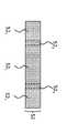
도 2(a)는 웨이퍼의 일부인 CMOS 센서(10)를 나타낸다. CMOS 센서(10)는 전면부와 후면부를 갖는 반도체 기판(20)을 포함한다. 기판(20)은 실리콘, 실리콘 게르마늄 등과 같은 일반적으로 알려진 반도체 물질들로 형성될 수 있다. 센서(10)는 기판(20)상에 형성된 픽셀 영역들 또는 센서 엘리먼트들의 그리드 또는 어레이를 포함할 수 있다. 이러한 하나의 센서 엘리먼트 또는 픽셀 영역(60)이 도 2(a)에서 예시로서 도시된다.2 (a) shows a
픽셀 영역(60)은 때때로 광다이오드라고 불리어지는 감광성 다이오드를 포함할 수 있으며, 이 감광성 다이오드는 자신에 부딪치는 광의 세기 또는 밝기에 관한 신호를 발생시킬 수 있다. 감광성 다이오드는 pnp 접합을 포함한 핀(pinned)층 광다이오드일 수 있다. 이와 달리 비 핀층 광다이오드가 이용될 수 있다. 본 실시예들과 함께 임의의 적절한 광다이오드가 이용될 수 있으며, 이러한 광다이오드들 모두는 본 실시예들의 범위내에 포함되는 것으로 한다. 픽셀 영역(60)은 트랜지스터를 더 포함할 수 있는데, 이 트랜지스터는 전송 트랜지스터, 리셋 트랜지스터, 소스 팔로워 트랜지스터, 또는 선택 트랜지스터일 수 있다. 트랜지스터는 기판에 인접해 있는 게이트 유전체, 게이트 유전체 위의 게이트 전극, 및 게이트 유전체와 게이트 전극의 측벽들을 따라 존재하는 스페이서들을 포함할 수 있다.
기판(20)은 기판상에서 형성된 다양한 디바이스들을 분리시키고 격리시키기 위해, 또한 이미지 센서의 다른 논리 영역들로부터 픽셀 영역들을 분리시키기 위한, 도시되지 않은 복수의 격리 영역들을 더 포함할 수 있다.
기판(20)의 후면부상에서, 칼라 이미징 응용들을 위해 기판(20)의 후면부 위의 유전체층상에 마이크로렌즈와 칼라 필터 엘리먼트(70)가 형성될 수 있다. 후면 조명된 광이 광감지 영역들상에 포커싱될 수 있도록, 마이크로렌즈들은 기판의 후면부와 칼라 필터 사이에 위치할 수 있다. 마이크로렌즈들은 기판의 후면부로부터 조명된 광을 광다이오드에 수렴시킨다. 칼라 필터 엘리먼트들 각각은 대응하는 마이크로렌즈들과 연계되어 있다. 칼라 필터 엘리먼트들 및 이와 연계된 마이크로렌즈들은 정렬 마크들을 이용하여 센서층의 감광성 엘리먼트들과 정렬될 수 있다.On the backside of the
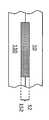
기판(20)의 전면부상에서는, 트랜지스터들과 같은 보다 많은 집적 회로들 및 캐패시터, 저항기 등과 같은 기타 디바이스들(미도시됨)이 형성될 수 있다. 상호연결 구조물(24)은 디바이스들 위에 형성될 수 있다. 상호접속 구조물(24)은 비제한적인 예시로서, 금속간 유전체(inter-metal dielectric; IMD)들, 패시베이션층들 등을 포함한 복수의 유전체층들(26)을 포함할 수 있다. IMD들(26)은 예컨대 약 2.5보다 작은 k 값들을 갖는 저 k 유전체 물질들로 형성될 수 있다. 금속선들(30)과 비아들(32)은 복수의 유전체층(26)에서 형성되고, 이것들은 잘 알려진 다마신 프로세스를 이용하여 구리로 형성될 수 있거나, 또는 알루미늄, 텅스텐, 은 등과 같은 다른 금속들로 형성될 수 있다.On the front side of the
상호연결 구조물(24)은 아래에 있는 집적 회로들을 상호연결시키고, 집적 회로들을 기판(20)의 전면부상에 형성되어 있는 각각의 접합 패드(42)와 접합 패드 어레이(52)에 연결시킨다. 접합 패드(42)는 활성 영역(11)이나 또는 접합 패드 영역(12)에서 형성될 수 있고, 접합 패드 어레이(52)는 접합 패드 어레이들(13 또는 14) 중 임의의 것일 수 있거나 또는 도 1(a)에서의 접합 패드 영역(12)에서 도시된 다른 것들일 수 있다. 접합 패드(42)는 접합 패드 어레이(52)에 의해 커버된 영역의 총체적인 크기(W2)에 비해 보다 작은 크기의 폭(W1)을 가질 수 있다. 예를 들어, W2는 대략 수십㎛ ~ 100㎛의 크기일 수 있다. 전체적인 센서(10), 가능하게는 전체적인 웨이퍼에 걸쳐, 임계 횡측 치수는 미리결정되고, 임계 횡측 치수보다 큰 횡측 치수(폭 및/또는 길이)를 갖는 임의의 접합 패드는 접합 패드 어레이(52)에서 도시된 바와 같은 접합 패드 어레이 형태를 가질 것인 반면에, 임계 횡측 치수보다 작은 횡측 치수들(폭 및/또는 길이)을 갖는 임의의 접합 패드는 접합 패드(42)로서 하나의 고형 접합 패드일 것이다. 예를 들어, 크기 20㎛의 미리결정된 치수가 임계치로서 역할을 할 수 있으며, 패드의 폭 또는 길이일 수 있는, 20㎛ 또는 그 이상의 크기를 갖는 임의의 패드는 접합 패드 어레이로서 형성될 수 있되, 그렇지 않은 크기를 갖는 임의의 패드는 단일 패드로서 형성될 수 있다.
접합 패드 어레이(52)에서는 단지 세 개의 접합 패드들만이 도시된다. 접합 패드 어레이(52) 내에서는 다른 갯수의 접합 패드들이 존재할 수 있다. 접합 패드 어레이(52) 내의 각각의 접합 패드는 서로 전기적으로 연결되어서 접합 패드 어레이(52)는 하나의 접촉부로서 기능을 하며, 때때로는, 이것은 패턴화된 접합 패드(52)로서 칭해질 수 있다. 접합 패드 어레이(52) 내의 접합 패드는 대략 5~20㎛의 폭과 길이의 유사한 크기를 가질 수 있다. 접합 패드 어레이(52) 내의 제1 접합 패드는 자신과 이웃해 있는 접합 패드로부터 대략 5~20㎛의 범위의 거리를 두면서 분리될 수 있다.Only three bond pads are shown in
접합 패드 어레이(52) 내의 접합 패드들간의 전기적 연결은 금속선(30')과 비아들(32')을 통해 이루어진다. 금속선(30')과 비아들(32')은 최상단 금속화층(Mtop이라고 통칭된다) 또는 재분배층일 수 있는, 접합 패드(52) 바로 아래의 금속화층(또는 패시베이션층 내부)에 존재할 수 있다. 이와 달리, 접합 패드 어레이(52) 내의 접합 패드들간의 전기적 연결은 바닥 금속화층(M1이라고 통칭된다)에서부터 최상단 금속화층(Mtop)의 범위에 이르는 아래의 금속화층들 중의 임의의 층에서 제공될 수 있다.Electrical connections between the bond pads in the
쓰루 비아(Through via; TV)들(40, 50)은 기판(20)을 관통하여 연장하며, 기판(20)의 전면부 상에 있는 피처(feature)들을 후면부에 상호연결시킨다. 쓰루 비아들(40, 50)는 예컨대, 쓰루 실리콘 비아, 쓰루 산화물 비아 등일 수 있다. 일반적으로, 위에서 언급한 바와 같이, 기판(20)은 실리콘 기판, 산화된 기판 등과 같은 다양한 물질들을 포함할 수 있다. 쓰루 비아들(40, 50)은 기판(20)을 관통하여 연장하는 비아들을 나타낸다. TV(40)는 접합 패드(42)에 전기적으로 연결되고, TV(50)는 접합 패드 어레이(52)에 전기적으로 연결된다. 따라서, 접합 패드(42)와 TV(40)는 비교적 작은 전류, 예컨대 신호 전류를 운송하기 위해 이용될 수 있는 반면에, 접합 패드 어레이(52)와 TV(50)는 상대적으로 큰 전류, 예컨대 전원 전류를 운송하기 위해 이용될 수 있다. 접합 패드(42)는 접합 패드 어레이(52)로부터 전기적으로 연결해제될 수 있다.Through vias (TVs) 40, 50 extend through the
도 2(b)는 접합 패드 어레이(52) 내의 접합 패드들이 기판(20)의 후면부에서 함께 연결되는 대안적인 실시예를 도시한다. 센서(10)의 후면부상에는, 접합 패드들(62, 72)이 형성될 수 있다. 기판(20)의 양쪽면들상에 있는 피처들을 상호연결하기 위해 하나의 TV를 이용하는 것 대신에, 하나 보다 많은 TV(501, 502, 503)가 접합 패드 어레이(52)를 기판의 후면부에 있는 접합 패드(72)에 전기적으로 상호연결시킬 수 있다. 실시예에서, 접합 패드들(62, 72)은 접합 패드(42) 및 접합 패드 어레이(52)의 사양과 유사한 사양을 각각 갖는다. 따라서, 접합 패드(72)는 접합 패드(62)보다 클 수 있다.2 (b) shows an alternative embodiment in which bond pads in
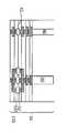
도 3(a) 내지 도 3(d)는 도 2(a)와 도 2(b)에서 도시된 접합 패드 어레이(52 또는 72)의 여러가지 잠재적인 설계들의 윗면들이다. 도 3(a)와 도 3(b) 모두는 개구들(53)에 의해 분리된 접합 패드(521), 및 접합 패드(521)에 연결하기 위한 상호연결부(522)를 포함한 접합 패드 어레이(52)를 도시한다. 상호연결부(522)는 또한 접합 패드(521)와 동일한 층에 있다.3A-3D are top surfaces of various potential designs of the
한편, 도 3(c)는 접합 패드 어레이(52)가 개구들(53)에 의해 분리된 복수의 개별적인 접합 패드들(521)을 포함하는 또 다른 실시예를 도시한다. 접합 패드 어레이(52)가 위치해 있는 층에서, 개별적인 접합 패드(521)간에는 어떠한 전기적 연결도 존재하지 않는다. 전기적 연결들은 도 2(a)에서 도시된 금속선(30') 및 비아들(32')과 같은, 아래에 위치한 비아들과 금속선들을 통해 제공된다. 도 3(a) 내지 도 3(c)에서 도시된 구조물을 갖춤으로써, 접합 패드 어레이(52)는 집적된 접합 패드로서 역할을 하는데, 이것은 임의의 접합 패드(521)로의 연결은 접합 패드 어레이 내의 다른 접합 패드들로의 연결에 등가적이라는 것을 의미한다.Meanwhile, FIG. 3 (c) shows another embodiment in which the
도 3(a)와 도 3(b)에서 도시된 실시예들, 및 도 3(c)에서 도시된 실시예 모두를 포함하도록 조합 방식들이 형성될 수 있다. 조합 방식들에서, 접합 패드들(521) 중 일부는 상호연결부(522)를 통해 그룹들로서 상호연결되는 반면에, 상호연결된 접합 패드들(521)의 상이한 그룹들은 서로로부터 연결해제된다. 도 3(d)에서는 각 열의 접합 패드들(521)이 상호연결되는 반면에, 열들은 분리되어 있는 예시적인 실시예가 도시된다. 다시, 도 2(a)에서 도시된 바와 같이, 아래에 있는 적어도 하나의 비아(32')가 각 열에 연결될 것이며, 비아들(32')은 상호연결될 것이다.Combinations may be formed to include both the embodiments shown in FIGS. 3A and 3B and the embodiment shown in FIG. 3C. In combination schemes, some of the
도 3(a) 내지 도 3(d)에서 도시된 바와 같이, 개구들(53)은 적어도 부분적으로 유전체 물질로 채워질 수 있다. 도 2(a)를 참조하면, 개구들(53) 중의 적어도 하단부들은 복수의 유전체층들(26) 중의 최상단 유전체층의 물질로 채워진다.As shown in FIGS. 3A-3D, the
도 3(a) 및 도 3(b)에서 도시된 실시예들이 채택되는 경우, 도 2(a)에서 도시된 바와 같이, 접합 패드들(521)에 연결된 하나 이상의 비아(32')가 존재할 수 있다. 이와 달리, 접합 패드들(521)은 이미 상호연결되어 있기 때문에, 도 2(a)에서 도시된 단하나의 비아(32')만이 도 3(a) 및 도 3(b)에서 도시된 바와 같은 접합 패드들(521) 중의 단하나의 접합 패드에 연결되도록 형성될 수 있다. 하지만, 도 3(c) 및 도 3(d)에서 도시된 실시예들이 채택되는 경우, 개별적인 접합 패드(521) 각각은 아래에 위치한 비아(32')에 연결되어야 한다. 그렇지 않은 경우에는, 연결된 비아(32')가 없는 접합 패드들은 다른 접합 패드들과 연결될 수 없을 것이다.If the embodiments shown in FIGS. 3 (a) and 3 (b) are adopted, as shown in FIG. 2 (a), there may be one or more vias 32 'connected to the
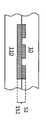
도 2(a)에서 도시된 단면도가 획득되는 바에 좌우되어, 접합 패드 어레이(52)의 단면도는 도 4(a)에서 도시된 고형 접합들로서 나타날 수 있거나, 또는 도 4(b)에 의해 표시된 바와 같이 하나의 연속적인 패드로서 나타날 수 있으며, 도 4(a)는 도 3(a)에서의 4A-4A 라인을 따라 절단한 평면을 바라본 단면도일 수 있는 반면에, 도 4(b)는 도 3(b)에서의 4B-4B 라인을 따라 절단한 평면을 바라본 단면도일 수 있다.Depending on what cross section shown in FIG. 2 (a) is obtained, the cross section of the
도 5는 센서(10)와 ASIC 칩(110)의 대면 접합을 나타낸다. ASIC 칩(110)은 도 2 내지 도 4에서 도시된 것과 동일하거나 또는 상이한 구조를 가질 수 있다. 유리하게도, 본 개시내용의 실시예들을 채용함으로써, 접합 패드 어레이들(52, 152)은 디싱 효과가 발생할 염려없이 형성될 수 있고, 이에 따라 결과적인 접합은 보다 신뢰적일 수 있고, 보다 큰 전류들을 도통시킬 수 있다. 접합 패드 어레이(152)는 ASIC의 기판의 전면부에서, ASIC(110)의 접합 패드 영역상에서 형성된다. 접합 패드 어레이(152)는 도 5에서 도시된 바와 같이 서로가 개구들에 의해 분리되어 있는 세 개의 접합 패드들을 포함한다. 접합 패드 어레이(152) 내에서는 다른 갯수의 접합 패드들이 존재할 수 있다. 접합 패드 어레이(152)의 접합 패드는 접합 패드 어레이(52)의 접합 패드에 도 5에서 도시된 일대일 방식으로 직접적으로 접합되고 연결된다. 이것은 센서(10)와 ASIC(110)을 함께 접합시키기 위한 선호된 방식일 수 있지만, 다른 접합 형태들이 가능할 수 있다. 예를 들어, 접합 패드 어레이(152)는 접합 패드 어레이(52)의 접합 패드 구성과는 상이한 구성을 가질 수 있다. 접합 패드 어레이(52)의 제1 접합 패드와 접합 패드 어레이(152)의 제3 접합 패드가 함께 접합되거나, 또는 이에 더하여, 접합 패드 어레이(52)의 제2 접합 패드와 접합 패드 어레이(152)의 제4 접합 패드가 함께 접합되는 바와 같이, 접합 패드 어레이(52)와 접합 패드 어레이(152)의 접합은 각각의 접합 패드 어레이에 대한 접합 패드 중 하나의 접합 패드상에서 형성될 수 있다.5 shows the face junction of the
도 6(a) 내지 도 6(c)는 접합 패드 어레이들(52, 152)간의 접합의 세 개의 잠재적인 단면도들을 나타내며, 상이한 도면들은, 도 4(a)와 도 4(b)에서 도시된 것과 같이, 상이한 위치들에서 단면도들을 취한 결과들이거나, 및/또는 동일하거나 또는 상이한 구조들을 갖는 접합 패드 어레이들(52, 152)을 형성한 결과들이다.6 (a)-(c) show three potential cross-sectional views of the junction between
센서(10)의 개시된 구조에서, 응용들 동안의 조명된 광은 가시광 빔으로 제한되지 않을 수 있으며, 적외선(IR) 및 자외선(UV)과 같은 다른 광학적 광, 및 다른 적절한 방사빔들로 확장될 수 있다.In the disclosed structure of the
본 개시내용의 실시예들 및 그 장점들을 자세하게 설명하였지만, 여기에 다양한 변경, 대체, 및 변동이 첨부된 청구범위들에 의해 정의된 본 발명개시의 범위 및 사상을 벗어나지 않고서 행해질 수 있다는 것을 이해해야 한다.While the embodiments of the present disclosure and the advantages thereof have been described in detail, it should be understood that various changes, substitutions and alterations herein can be made without departing from the scope and spirit of the disclosure as defined by the appended claims. .
또한, 본 출원의 범위는 상세한 설명에서 설명된 물질, 수단, 방법, 및 단계의 프로세스, 머신, 제품, 구성의 특정한 실시예들로 한정되는 것을 의도하지 않는다. 본 발명분야의 당업자라면 여기서 설명된 대응하는 실시예들과 실질적으로 동일한 기능을 수행하거나 또는 이와 실질적으로 동일한 결과를 달성하는, 현존하거나 후에 개발될 물질, 수단, 방법, 또는 단계의 공정, 머신, 제조, 조성이 본 개시내용에 따라 이용될 수 있다는 것을 본 개시내용으로부터 손쉽게 알 것이다. 따라서, 첨부된 청구항들은 이와 같은 물질, 수단, 방법, 또는 단계의 공정, 머신, 제조, 조성을 청구항의 범위내에 포함하는 것으로 한다.Further, the scope of the present application is not intended to be limited to the specific embodiments of the materials, means, methods, and steps of the process, machine, article, or construction set forth in the detailed description. Means, methods, or steps of a material, means, method, or step to be developed that will perform substantially the same function or achieve substantially the same result as those of the corresponding embodiments described herein, Manufacturing, and composition of the present invention may be utilized in accordance with the present disclosure. Accordingly, the appended claims are intended to cover within the scope of the claims the process, machine, manufacture, composition of such material, means, method, or step.
Claims (10)
Translated fromKorean전면부와 후면부를 갖는 기판;
상기 기판의 활성 영역 내의 감광성 다이오드; 및
상기 기판의 전면부에 있는 제1 접합 패드 어레이를 포함하며, 상기 제1 접합 패드 어레이는, 개구에 의해 서로 분리되어 있되 서로 전기적으로 연결되어 있으며 하나의 전기적 접촉부로서 기능을 하는 제1 접합 패드와 제2 접합 패드를 포함한 것인, 후면 조명(BSI) 센서 디바이스.A backside illuminated (BSI) sensor device, comprising:
A substrate having a front portion and a rear portion;
A photosensitive diode in the active region of the substrate; And
A first bond pad array in a front portion of the substrate, the first bond pad array being separated from each other by an opening, the first bond pad being electrically connected to each other and functioning as an electrical contact; A back lit (BSI) sensor device comprising a second bond pad.
기판, 및 상기 기판의 전면부에 있는 제2 접합 패드 어레이를 포함한 ASIC 칩을 더 포함하며, 상기 제2 접합 패드 어레이는, 서로 분리되어 있되 서로 전기적으로 연결되어 있으며 하나의 전기적 접촉부로서 기능을 하는 제3 접합 패드와 제4 접합 패드를 포함하며,
상기 제1 접합 패드 어레이의 상기 제1 접합 패드와 상기 제2 접합 패드 어레이의 상기 제3 접합 패드는 함께 접합되는 것인, 후면 조명(BSI) 센서 디바이스.The method of claim 1,
And an ASIC chip comprising a substrate, and a second bond pad array on the front side of the substrate, the second bond pad array being separated from each other but electrically connected to each other and functioning as one electrical contact. A third bonding pad and a fourth bonding pad,
And the first bond pad of the first bond pad array and the third bond pad of the second bond pad array are bonded together.
센서 디바이스와,
ASIC 칩을 포함하고,
상기 센서 디바이스는,
전면부와 후면부를 갖는 기판;
상기 기판의 활성 영역 내의 감광성 다이오드; 및
상기 기판의 전면부에 있는 제1 접합 패드 어레이를 포함하며, 상기 제1 접합 패드 어레이는, 개구에 의해 서로 분리되어 있되 서로 전기적으로 연결되어 있으며 하나의 전기적 접촉부로서 기능을 하는 제1 접합 패드와 제2 접합 패드를 포함하며,
상기 ASIC 칩은,
기판과,
상기 기판의 전면부에 있는 제2 접합 패드 어레이를 포함하고, 상기 제2 접합 패드 어레이는, 개구에 의해 서로 분리되어 있되 서로 전기적으로 연결되어 있으며 하나의 전기적 접촉부로서 기능을 하는 제3 접합 패드와 제4 접합 패드를 포함하며,
상기 제1 접합 패드 어레이의 상기 제1 접합 패드와 상기 제2 접합 패드 어레이의 상기 제3 접합 패드는 함께 접합되는 것인, 집적 회로(IC) 패키지.In an integrated circuit (IC) package,
A sensor device,
Including ASIC chip,
The sensor device,
A substrate having a front portion and a rear portion;
A photosensitive diode in the active region of the substrate; And
A first bond pad array in a front portion of the substrate, the first bond pad array being separated from each other by an opening, the first bond pad being electrically connected to each other and functioning as an electrical contact; A second bonding pad,
The ASIC chip,
A substrate;
A second bond pad array in a front portion of the substrate, the second bond pad array being separated from each other by an opening and electrically connected to each other and having a third bond pad functioning as an electrical contact; A fourth bonding pad,
And the first bond pad of the first bond pad array and the third bond pad of the second bond pad array are bonded together.
Applications Claiming Priority (2)
| Application Number | Priority Date | Filing Date | Title |
|---|---|---|---|
| US13/547,269US8710607B2 (en) | 2012-07-12 | 2012-07-12 | Method and apparatus for image sensor packaging |
| US13/547,269 | 2012-07-12 |
Publications (1)
| Publication Number | Publication Date |
|---|---|
| KR20140008983Atrue KR20140008983A (en) | 2014-01-22 |
Family
ID=49913277
Family Applications (1)
| Application Number | Title | Priority Date | Filing Date |
|---|---|---|---|
| KR1020120109897ACeasedKR20140008983A (en) | 2012-07-12 | 2012-10-04 | Method and apparatus for image sensor packaging |
Country Status (3)
| Country | Link |
|---|---|
| US (3) | US8710607B2 (en) |
| KR (1) | KR20140008983A (en) |
| CN (1) | CN103545324B (en) |
Cited By (8)
| Publication number | Priority date | Publication date | Assignee | Title |
|---|---|---|---|---|
| KR20180097522A (en)* | 2015-12-21 | 2018-08-31 | 소니 주식회사 | Solid-state imaging devices and electronic devices |
| KR20190058345A (en)* | 2017-11-21 | 2019-05-29 | 타이완 세미콘덕터 매뉴팩쳐링 컴퍼니 리미티드 | Anchor structures and methods for uniform wafer planarization and bonding |
| KR20190064500A (en)* | 2017-11-30 | 2019-06-10 | 타이완 세미콘덕터 매뉴팩쳐링 컴퍼니 리미티드 | Semiconductor device and method for fabricating the same |
| KR20200002698A (en)* | 2018-06-29 | 2020-01-08 | 타이완 세미콘덕터 매뉴팩쳐링 컴퍼니 리미티드 | Semiconductor interconnect structure and method |
| US10672820B2 (en) | 2017-11-23 | 2020-06-02 | Taiwan Semiconductor Manufacturing Co., Ltd. | Hybrid bonded structure |
| KR20200093195A (en)* | 2019-01-28 | 2020-08-05 | 삼성전자주식회사 | Semiconductor device having bonding pads |
| US10879293B2 (en) | 2016-12-20 | 2020-12-29 | Sony Semiconductor Solutions Corporation | Solid-state imaging device, method of manufacturing solid-state imaging device, and electronic device |
| US11817472B2 (en) | 2017-11-21 | 2023-11-14 | Taiwan Semiconductor Manufacturing Co., Ltd. | Anchor structures and methods for uniform wafer planarization and bonding |
Families Citing this family (14)
| Publication number | Priority date | Publication date | Assignee | Title |
|---|---|---|---|---|
| TWI676279B (en)* | 2013-10-04 | 2019-11-01 | 新力股份有限公司 | Semiconductor device and solid-state imaging device |
| US9679936B2 (en) | 2014-02-27 | 2017-06-13 | Semiconductor Components Industries, Llc | Imaging systems with through-oxide via connections |
| TWI692859B (en)* | 2015-05-15 | 2020-05-01 | 日商新力股份有限公司 | Solid-state imaging device, manufacturing method thereof, and electronic device |
| JP6856983B2 (en)* | 2016-06-30 | 2021-04-14 | キヤノン株式会社 | Photoelectric converter and camera |
| KR102051373B1 (en)* | 2016-09-23 | 2019-12-04 | 삼성전자주식회사 | Fan-out sensor package and camera module comprising the same |
| US10178764B2 (en)* | 2017-06-05 | 2019-01-08 | Waymo Llc | PCB optical isolation by nonuniform catch pad stack |
| DE102018125106B4 (en) | 2017-11-23 | 2023-10-05 | Taiwan Semiconductor Manufacturing Co., Ltd. | Hybrid bonded structure and process for its production |
| EP3525232A1 (en)* | 2018-02-09 | 2019-08-14 | Nexperia B.V. | Semiconductor device and method of manufacturing the same |
| CN112292757B (en)* | 2018-08-24 | 2024-03-05 | 铠侠股份有限公司 | Semiconductor device and manufacturing method thereof |
| CN110112097A (en)* | 2019-05-21 | 2019-08-09 | 德淮半导体有限公司 | The production method of wafer bonding structure and wafer bonding structure |
| CN110391147A (en)* | 2019-07-26 | 2019-10-29 | 德淮半导体有限公司 | Pad structure and method of forming the same |
| KR20220033619A (en) | 2020-09-08 | 2022-03-17 | 삼성전자주식회사 | Semiconductor package |
| CN113629087B (en)* | 2021-08-06 | 2023-12-22 | 武汉新芯集成电路制造有限公司 | BSI image sensor device and manufacturing method thereof |
| CN115910825A (en)* | 2022-11-15 | 2023-04-04 | 上海华力微电子有限公司 | On-line monitoring method of pad structure and photolithography splicing process |
Family Cites Families (26)
| Publication number | Priority date | Publication date | Assignee | Title |
|---|---|---|---|---|
| US6020629A (en)* | 1998-06-05 | 2000-02-01 | Micron Technology, Inc. | Stacked semiconductor package and method of fabrication |
| US8021976B2 (en)* | 2002-10-15 | 2011-09-20 | Megica Corporation | Method of wire bonding over active area of a semiconductor circuit |
| US7189595B2 (en)* | 2001-05-31 | 2007-03-13 | International Business Machines Corporation | Method of manufacture of silicon based package and devices manufactured thereby |
| US6510195B1 (en)* | 2001-07-18 | 2003-01-21 | Koninklijke Philips Electronics, N.V. | Solid state x-radiation detector modules and mosaics thereof, and an imaging method and apparatus employing the same |
| US7282382B2 (en)* | 2001-10-29 | 2007-10-16 | Stmicroelectronics N.V. | Method for producing a photodiode contact for a TFA image sensor |
| JP3778445B2 (en)* | 2003-03-27 | 2006-05-24 | 富士通株式会社 | Semiconductor device |
| US20060001180A1 (en)* | 2004-06-30 | 2006-01-05 | Brian Taggart | In-line wire bonding on a package, and method of assembling same |
| US7973380B2 (en)* | 2005-11-23 | 2011-07-05 | Taiwan Semiconductor Manufacturing Company, Ltd. | Method for providing metal extension in backside illuminated sensor for wafer level testing |
| KR100801447B1 (en)* | 2006-06-19 | 2008-02-11 | (주)실리콘화일 | Image sensor using back light photodiode and manufacturing method thereof |
| US7622364B2 (en)* | 2006-08-18 | 2009-11-24 | International Business Machines Corporation | Bond pad for wafer and package for CMOS imager |
| US20080246152A1 (en)* | 2007-04-04 | 2008-10-09 | Taiwan Semiconductor Manufacturing Co., Ltd. | Semiconductor device with bonding pad |
| JP4609497B2 (en)* | 2008-01-21 | 2011-01-12 | ソニー株式会社 | Solid-state imaging device, manufacturing method thereof, and camera |
| US7982177B2 (en)* | 2008-01-31 | 2011-07-19 | Omnivision Technologies, Inc. | Frontside illuminated image sensor comprising a complex-shaped reflector |
| US8101978B2 (en)* | 2008-02-08 | 2012-01-24 | Omnivision Technologies, Inc. | Circuit and photo sensor overlap for backside illumination image sensor |
| US7859033B2 (en)* | 2008-07-09 | 2010-12-28 | Eastman Kodak Company | Wafer level processing for backside illuminated sensors |
| US7973310B2 (en) | 2008-07-11 | 2011-07-05 | Chipmos Technologies Inc. | Semiconductor package structure and method for manufacturing the same |
| US9041841B2 (en)* | 2008-10-10 | 2015-05-26 | Taiwan Semiconductor Manufacturing Company, Ltd. | Image sensor having enhanced backside illumination quantum efficiency |
| US8053900B2 (en) | 2008-10-21 | 2011-11-08 | Taiwan Semiconductor Manufacturing Company, Ltd. | Through-substrate vias (TSVs) electrically connected to a bond pad design with reduced dishing effect |
| US8125042B2 (en)* | 2008-11-13 | 2012-02-28 | Samsung Electronics Co., Ltd. | Semiconductor package and method of manufacturing the same |
| US9142586B2 (en)* | 2009-02-24 | 2015-09-22 | Taiwan Semiconductor Manufacturing Company, Ltd. | Pad design for backside illuminated image sensor |
| JP5985136B2 (en) | 2009-03-19 | 2016-09-06 | ソニー株式会社 | SEMICONDUCTOR DEVICE, ITS MANUFACTURING METHOD, AND ELECTRONIC DEVICE |
| TWI420662B (en)* | 2009-12-25 | 2013-12-21 | Sony Corp | Semiconductor component, method of manufacturing the same, and electronic device |
| JP5685898B2 (en)* | 2010-01-08 | 2015-03-18 | ソニー株式会社 | Semiconductor device, solid-state imaging device, and camera system |
| US8431977B2 (en)* | 2010-06-10 | 2013-04-30 | Megica Corporation | Wafer level processing method and structure to manufacture semiconductor chip |
| JP2012079979A (en)* | 2010-10-04 | 2012-04-19 | Sony Corp | Solid-state imaging device, method for manufacturing the same, and electronic apparatus |
| US8604576B2 (en)* | 2011-07-19 | 2013-12-10 | Opitz, Inc. | Low stress cavity package for back side illuminated image sensor, and method of making same |
- 2012
- 2012-07-12USUS13/547,269patent/US8710607B2/enactiveActive
- 2012-10-04KRKR1020120109897Apatent/KR20140008983A/ennot_activeCeased
- 2012-10-25CNCN201210414021.9Apatent/CN103545324B/enactiveActive
- 2014
- 2014-03-11USUS14/204,921patent/US9029183B2/enactiveActive
- 2015
- 2015-05-01USUS14/702,450patent/US9917123B2/enactiveActive
Cited By (12)
| Publication number | Priority date | Publication date | Assignee | Title |
|---|---|---|---|---|
| KR20180097522A (en)* | 2015-12-21 | 2018-08-31 | 소니 주식회사 | Solid-state imaging devices and electronic devices |
| US10879293B2 (en) | 2016-12-20 | 2020-12-29 | Sony Semiconductor Solutions Corporation | Solid-state imaging device, method of manufacturing solid-state imaging device, and electronic device |
| KR20190058345A (en)* | 2017-11-21 | 2019-05-29 | 타이완 세미콘덕터 매뉴팩쳐링 컴퍼니 리미티드 | Anchor structures and methods for uniform wafer planarization and bonding |
| US11152417B2 (en) | 2017-11-21 | 2021-10-19 | Taiwan Semiconductor Manufacturing Co., Ltd. | Anchor structures and methods for uniform wafer planarization and bonding |
| US11817472B2 (en) | 2017-11-21 | 2023-11-14 | Taiwan Semiconductor Manufacturing Co., Ltd. | Anchor structures and methods for uniform wafer planarization and bonding |
| US10672820B2 (en) | 2017-11-23 | 2020-06-02 | Taiwan Semiconductor Manufacturing Co., Ltd. | Hybrid bonded structure |
| KR20210066770A (en)* | 2017-11-23 | 2021-06-07 | 타이완 세미콘덕터 매뉴팩쳐링 컴퍼니 리미티드 | Hybrid bonded structure |
| KR20190064500A (en)* | 2017-11-30 | 2019-06-10 | 타이완 세미콘덕터 매뉴팩쳐링 컴퍼니 리미티드 | Semiconductor device and method for fabricating the same |
| KR20200002698A (en)* | 2018-06-29 | 2020-01-08 | 타이완 세미콘덕터 매뉴팩쳐링 컴퍼니 리미티드 | Semiconductor interconnect structure and method |
| US11424205B2 (en) | 2018-06-29 | 2022-08-23 | Taiwan Semiconductor Manufacturing Company, Ltd. | Semiconductor interconnect structure and method |
| US12154876B2 (en) | 2018-06-29 | 2024-11-26 | Taiwan Semiconductor Manufacturing Company, Ltd. | Semiconductor interconnect structure and method |
| KR20200093195A (en)* | 2019-01-28 | 2020-08-05 | 삼성전자주식회사 | Semiconductor device having bonding pads |
Also Published As
| Publication number | Publication date |
|---|---|
| US9029183B2 (en) | 2015-05-12 |
| US8710607B2 (en) | 2014-04-29 |
| US20150236064A1 (en) | 2015-08-20 |
| US20140015084A1 (en) | 2014-01-16 |
| CN103545324B (en) | 2016-12-21 |
| US9917123B2 (en) | 2018-03-13 |
| US20140193940A1 (en) | 2014-07-10 |
| CN103545324A (en) | 2014-01-29 |
Similar Documents
| Publication | Publication Date | Title |
|---|---|---|
| US9029183B2 (en) | Method and apparatus for image sensor packaging | |
| US10096645B2 (en) | Method and apparatus for image sensor packaging | |
| US10930699B2 (en) | Method and apparatus for image sensor packaging | |
| JP5843475B2 (en) | Solid-state imaging device and method for manufacturing solid-state imaging device | |
| US9087760B2 (en) | Semiconductor device and method of manufacturing the same, and electronic apparatus | |
| US9006807B2 (en) | Solid-state image sensing device and camera | |
| JP5532867B2 (en) | SOLID-STATE IMAGING DEVICE, ITS MANUFACTURING METHOD, SOLID-STATE IMAGING ELEMENT MANUFACTURING METHOD, AND SEMICONDUCTOR DEVICE | |
| US20100237452A1 (en) | Semiconductor device and backside illumination solid-state imaging device | |
| US9324744B2 (en) | Solid-state image sensor having a trench and method of manufacturing the same | |
| CN101005090A (en) | Back-illuminated image sensing element, its forming method and packaging | |
| TWI389330B (en) | Back side illumination imager and method of manufacturing same | |
| US8895936B2 (en) | Pixel array and image sensor including the same | |
| JP2019195082A (en) | Solid-state imaging device and method for manufacturing solid-state imaging device | |
| CN107425026A (en) | Semiconductor devices and its manufacture method | |
| KR20250083403A (en) | Combined short-wave infrared and visible light sensor, imager including same, and method for manufacturing same | |
| CN120344010A (en) | Image Sensor |
Legal Events
| Date | Code | Title | Description |
|---|---|---|---|
| A201 | Request for examination | ||
| PA0109 | Patent application | Patent event code:PA01091R01D Comment text:Patent Application Patent event date:20121004 | |
| PA0201 | Request for examination | ||
| E902 | Notification of reason for refusal | ||
| PE0902 | Notice of grounds for rejection | Comment text:Notification of reason for refusal Patent event date:20130923 Patent event code:PE09021S01D | |
| AMND | Amendment | ||
| PG1501 | Laying open of application | ||
| E601 | Decision to refuse application | ||
| PE0601 | Decision on rejection of patent | Patent event date:20140528 Comment text:Decision to Refuse Application Patent event code:PE06012S01D Patent event date:20130923 Comment text:Notification of reason for refusal Patent event code:PE06011S01I | |
| AMND | Amendment | ||
| PX0901 | Re-examination | Patent event code:PX09011S01I Patent event date:20140528 Comment text:Decision to Refuse Application Patent event code:PX09012R01I Patent event date:20131223 Comment text:Amendment to Specification, etc. | |
| PX0601 | Decision of rejection after re-examination | Comment text:Decision to Refuse Application Patent event code:PX06014S01D Patent event date:20140811 Comment text:Amendment to Specification, etc. Patent event code:PX06012R01I Patent event date:20140630 Comment text:Decision to Refuse Application Patent event code:PX06011S01I Patent event date:20140528 Comment text:Amendment to Specification, etc. Patent event code:PX06012R01I Patent event date:20131223 Comment text:Notification of reason for refusal Patent event code:PX06013S01I Patent event date:20130923 | |
| J201 | Request for trial against refusal decision | ||
| PJ0201 | Trial against decision of rejection | Patent event date:20141111 Comment text:Request for Trial against Decision on Refusal Patent event code:PJ02012R01D Patent event date:20140811 Comment text:Decision to Refuse Application Patent event code:PJ02011S01I Patent event date:20140528 Comment text:Decision to Refuse Application Patent event code:PJ02011S01I Appeal kind category:Appeal against decision to decline refusal Appeal identifier:2014101006983 Request date:20141111 | |
| J301 | Trial decision | Free format text:TRIAL DECISION FOR APPEAL AGAINST DECISION TO DECLINE REFUSAL REQUESTED 20141111 Effective date:20160122 | |
| PJ1301 | Trial decision | Patent event code:PJ13011S01D Patent event date:20160122 Comment text:Trial Decision on Objection to Decision on Refusal Appeal kind category:Appeal against decision to decline refusal Request date:20141111 Decision date:20160122 Appeal identifier:2014101006983 |