KR20140008497A - Optical device and method for machining optical device - Google Patents
Optical device and method for machining optical deviceDownload PDFInfo
- Publication number
- KR20140008497A KR20140008497AKR1020130072819AKR20130072819AKR20140008497AKR 20140008497 AKR20140008497 AKR 20140008497AKR 1020130072819 AKR1020130072819 AKR 1020130072819AKR 20130072819 AKR20130072819 AKR 20130072819AKR 20140008497 AKR20140008497 AKR 20140008497A
- Authority
- KR
- South Korea
- Prior art keywords
- optical device
- angle
- device wafer
- vertical line
- wafer
- Prior art date
- Legal status (The legal status is an assumption and is not a legal conclusion. Google has not performed a legal analysis and makes no representation as to the accuracy of the status listed.)
- Granted
Links
Images


Classifications
- H—ELECTRICITY
- H01—ELECTRIC ELEMENTS
- H01L—SEMICONDUCTOR DEVICES NOT COVERED BY CLASS H10
- H01L21/00—Processes or apparatus adapted for the manufacture or treatment of semiconductor or solid state devices or of parts thereof
- H01L21/70—Manufacture or treatment of devices consisting of a plurality of solid state components formed in or on a common substrate or of parts thereof; Manufacture of integrated circuit devices or of parts thereof
- H01L21/77—Manufacture or treatment of devices consisting of a plurality of solid state components or integrated circuits formed in, or on, a common substrate
- H01L21/78—Manufacture or treatment of devices consisting of a plurality of solid state components or integrated circuits formed in, or on, a common substrate with subsequent division of the substrate into plural individual devices
- B—PERFORMING OPERATIONS; TRANSPORTING
- B23—MACHINE TOOLS; METAL-WORKING NOT OTHERWISE PROVIDED FOR
- B23K—SOLDERING OR UNSOLDERING; WELDING; CLADDING OR PLATING BY SOLDERING OR WELDING; CUTTING BY APPLYING HEAT LOCALLY, e.g. FLAME CUTTING; WORKING BY LASER BEAM
- B23K26/00—Working by laser beam, e.g. welding, cutting or boring
- B23K26/36—Removing material
- B23K26/362—Laser etching
- B23K26/364—Laser etching for making a groove or trench, e.g. for scribing a break initiation groove
- B—PERFORMING OPERATIONS; TRANSPORTING
- B23—MACHINE TOOLS; METAL-WORKING NOT OTHERWISE PROVIDED FOR
- B23K—SOLDERING OR UNSOLDERING; WELDING; CLADDING OR PLATING BY SOLDERING OR WELDING; CUTTING BY APPLYING HEAT LOCALLY, e.g. FLAME CUTTING; WORKING BY LASER BEAM
- B23K26/00—Working by laser beam, e.g. welding, cutting or boring
- B23K26/36—Removing material
- B23K26/38—Removing material by boring or cutting
- B—PERFORMING OPERATIONS; TRANSPORTING
- B23—MACHINE TOOLS; METAL-WORKING NOT OTHERWISE PROVIDED FOR
- B23K—SOLDERING OR UNSOLDERING; WELDING; CLADDING OR PLATING BY SOLDERING OR WELDING; CUTTING BY APPLYING HEAT LOCALLY, e.g. FLAME CUTTING; WORKING BY LASER BEAM
- B23K26/00—Working by laser beam, e.g. welding, cutting or boring
- B23K26/36—Removing material
- B23K26/40—Removing material taking account of the properties of the material involved
- H—ELECTRICITY
- H10—SEMICONDUCTOR DEVICES; ELECTRIC SOLID-STATE DEVICES NOT OTHERWISE PROVIDED FOR
- H10H—INORGANIC LIGHT-EMITTING SEMICONDUCTOR DEVICES HAVING POTENTIAL BARRIERS
- H10H20/00—Individual inorganic light-emitting semiconductor devices having potential barriers, e.g. light-emitting diodes [LED]
- H10H20/01—Manufacture or treatment
- H—ELECTRICITY
- H10—SEMICONDUCTOR DEVICES; ELECTRIC SOLID-STATE DEVICES NOT OTHERWISE PROVIDED FOR
- H10H—INORGANIC LIGHT-EMITTING SEMICONDUCTOR DEVICES HAVING POTENTIAL BARRIERS
- H10H20/00—Individual inorganic light-emitting semiconductor devices having potential barriers, e.g. light-emitting diodes [LED]
- H10H20/80—Constructional details
- H10H20/81—Bodies
- H10H20/819—Bodies characterised by their shape, e.g. curved or truncated substrates
- B—PERFORMING OPERATIONS; TRANSPORTING
- B23—MACHINE TOOLS; METAL-WORKING NOT OTHERWISE PROVIDED FOR
- B23K—SOLDERING OR UNSOLDERING; WELDING; CLADDING OR PLATING BY SOLDERING OR WELDING; CUTTING BY APPLYING HEAT LOCALLY, e.g. FLAME CUTTING; WORKING BY LASER BEAM
- B23K2103/00—Materials to be soldered, welded or cut
- B23K2103/16—Composite materials, e.g. fibre reinforced
- B23K2103/166—Multilayered materials
- B23K2103/172—Multilayered materials wherein at least one of the layers is non-metallic
- B—PERFORMING OPERATIONS; TRANSPORTING
- B23—MACHINE TOOLS; METAL-WORKING NOT OTHERWISE PROVIDED FOR
- B23K—SOLDERING OR UNSOLDERING; WELDING; CLADDING OR PLATING BY SOLDERING OR WELDING; CUTTING BY APPLYING HEAT LOCALLY, e.g. FLAME CUTTING; WORKING BY LASER BEAM
- B23K2103/00—Materials to be soldered, welded or cut
- B23K2103/50—Inorganic material, e.g. metals, not provided for in B23K2103/02 – B23K2103/26
Landscapes
- Engineering & Computer Science (AREA)
- Physics & Mathematics (AREA)
- Optics & Photonics (AREA)
- Mechanical Engineering (AREA)
- Plasma & Fusion (AREA)
- Chemical & Material Sciences (AREA)
- General Physics & Mathematics (AREA)
- Condensed Matter Physics & Semiconductors (AREA)
- Inorganic Chemistry (AREA)
- Manufacturing & Machinery (AREA)
- Computer Hardware Design (AREA)
- Microelectronics & Electronic Packaging (AREA)
- Power Engineering (AREA)
- Composite Materials (AREA)
- Materials Engineering (AREA)
- Dicing (AREA)
- Led Devices (AREA)
- Laser Beam Processing (AREA)
Abstract
Description
Translated fromKorean본 발명은, 광 디바이스 및 광 디바이스의 가공 방법에 관한 것이다.The present invention relates to an optical device and a method of processing an optical device.
레이저 다이오드(LD)나 발광 다이오드(LED) 등의 광 디바이스의 제조 프로세스에서는, 사파이어나 SiC 등으로 이루어지는 결정 성장용 기판의 상면에 예컨대 에피택셜 성장에 의해 복수의 광 디바이스를 갖는 발광층(에피택셜층)이 적층된 광 디바이스 웨이퍼가 제조된다.In a manufacturing process of an optical device such as a laser diode (LD) or a light emitting diode (LED), a light emitting layer having a plurality of optical devices is formed on the upper surface of a substrate for crystal growth made of sapphire or SiC by epitaxial growth, ) Is fabricated.
LD, LED 등의 광 디바이스는, 격자형으로 설정된 분할 예정 라인으로 구획된 각 영역에 형성되고, 광 디바이스 웨이퍼를 분할 예정 라인을 따라 분할하여 개편화함으로써, 개개의 광 디바이스 칩이 제조된다.An optical device such as an LD or an LED is formed in each region partitioned by a line to be divided set in a lattice pattern and an optical device chip is manufactured by dividing the optical device wafer along a line to be divided and dividing the optical device wafer into individual pieces.
종래, 광 디바이스 웨이퍼를 분할 예정 라인을 따라 분할하는 방법으로서, 분할 예정 라인을 따라 웨이퍼에 대하여 흡수성을 갖는 파장의 펄스 레이저빔을 조사하여 레이저 가공 홈을 형성하고, 웨이퍼에 외력을 부여하는 것에 의해 레이저 가공 홈을 분할 기점으로 하여 광 디바이스 웨이퍼를 할단하는 방법이 알려져 있다(일본 특허 공개 평10-305420호 공보 참조).Conventionally, as a method of dividing an optical device wafer along a line to be divided along a line to be divided, a pulse laser beam of a wavelength having absorbency is irradiated to a wafer along a line to be divided to form a laser machining groove and an external force is given to the wafer A method of cutting an optical device wafer using a laser machining groove as a dividing point is known (see Japanese Patent Application Laid-Open No. 10-305420).
한편, 광 디바이스의 휘도 향상을 위해, 광 디바이스 웨이퍼에 대하여 투과성을 갖는 파장의 펄스 레이저빔을 웨이퍼의 내부에 집광점을 맞춰 조사하여 내부에 분할 예정 라인을 따른 개질층을 형성하고, 이 개질층에서 강도가 저하된 분할 예정 라인에 외력을 부여하는 것에 의해 광 디바이스 웨이퍼를 분할하는 방법도 제안되어 있다(예컨대 일본 특허 공개 제2008-006492호 공보 참조).On the other hand, in order to improve the brightness of an optical device, a pulse laser beam having a transmittance with respect to an optical device wafer is irradiated with a light-converging point in the wafer to form a modified layer along the line to be divided, A method of dividing an optical device wafer by applying an external force to a line to be divided with a reduced strength in the optical device wafer has been proposed (see, for example, Japanese Patent Application Laid-Open No. 2008-006492).
LED 등의 광 디바이스는, 보다 높은 휘도가 요구되고, 광 취출 효율의 향상이 요망되고 있다. 종래의 광 디바이스의 가공 방법에서는, 레이저빔을 광 디바이스 웨이퍼에 대하여 대략 수직으로 입사시켜, 레이저 가공 홈 또는 개질층을 분할 기점으로 광 디바이스 웨이퍼를 개개의 광 디바이스 칩으로 분할하고 있기 때문에, 광 디바이스 칩의 측면은 표면에 형성된 발광층에 대하여 대략 수직으로 가공되고, 광 디바이스는 직방체 형상을 이루고 있다.BACKGROUND ART [0002] Optical devices such as LEDs are required to have higher luminance, and it is desired to improve the light extraction efficiency. In the conventional optical device processing method, since the laser beam is made incident substantially perpendicularly to the optical device wafer, and the optical device wafer is divided into the individual optical device chips with the laser processing groove or the modified layer as the division origin, The side surface of the chip is processed substantially perpendicular to the light emitting layer formed on the surface, and the optical device has a rectangular parallelepiped shape.
따라서, 발광층으로부터 출사한 광은 측면에서 전반사하는 비율이 높아져, 전반사를 반복하는 동안에 최종적으로 광 디바이스 칩의 내부에서 소광되어 버리는 비율이 높아진다.Therefore, the ratio of the light emitted from the light emitting layer to the total reflection on the side surface increases, and the ratio of the light emitted from the light device chip to the light emitting device is increased during the total reflection.
본 발명은 이러한 점을 감안하여 이루어진 것이며, 그 목적으로 하는 점은, 광 취출 효율을 향상시킬 수 있는 광 디바이스 및 광 디바이스의 가공 방법을 제공하는 것이다.An object of the present invention is to provide an optical device and a method of processing an optical device that can improve light extraction efficiency.
청구항 1 기재의 발명에 의하면, 광 디바이스로서, 발광층을 갖는 사각형의 표면과, 이 표면과 평행한 사각형의 이면과, 상기 표면과 이면을 연결하는 제1 내지 제4 측면을 구비하며, 제1 측면은 상기 표면의 수직선으로부터 제1 각도 경사지고, 상기 제1 측면에 대면하는 제2 측면은 상기 수직선으로부터 제2 각도 경사지며, 제3 측면은 상기 수직선으로부터 제3 각도 경사지고, 상기 제3 측면에 대면하는 제4 측면은 상기 수직선으로부터 제4 각도 경사지는 것을 특징으로 하는 광 디바이스가 제공된다.According to a first aspect of the present invention, there is provided an optical device comprising: a rectangular surface having a light emitting layer; a rectangular back surface parallel to the surface; and first to fourth side surfaces connecting the front surface and the back surface, The second side facing the first side is inclined at a second angle from the vertical line, the third side is inclined at a third angle from the vertical line, and the third side is inclined at a third angle from the vertical line, And the fourth facing side is inclined at a fourth angle from the vertical line.
바람직하게는, 광 디바이스는, 표면으로부터 이면에 이르는 단면 형상이 평행사변형 또는 사다리꼴이다. 바람직하게는, 제1 내지 제4 각도는 모두 동일 각도로 설정되어 있다.Preferably, the optical device has a parallelogram shape or a trapezoidal cross-sectional shape extending from the surface to the back surface. Preferably, the first to fourth angles are all set to the same angle.
청구항 5 기재의 발명에 의하면, 청구항 1 내지 청구항 4 중 어느 한 항에 기재된 광 디바이스의 가공 방법으로서, 표면에 발광층을 갖고, 복수의 교차하는 분할 예정 라인이 설정되며, 이 분할 예정 라인으로 구획된 상기 발광층의 각 영역에 각각 광 디바이스를 갖는 광 디바이스 웨이퍼를 준비하는 웨이퍼 준비 단계와, 광 디바이스 웨이퍼에 상기 광 디바이스의 상기 제1 내지 제4 측면에 대응한 복수의 경사면을 설정하는 경사면 설정 단계와, 이 경사면 설정 단계를 실시한 후, 광 디바이스 웨이퍼에 대하여 흡수성을 갖는 파장의 레이저빔을 상기 경사면을 따라 조사하여 상기 경사면을 따른 레이저 가공 홈을 형성하는 레이저 가공 단계를 포함하는 것을 특징으로 하는 광 디바이스의 가공 방법이 제공된다.According to a fifth aspect of the present invention, there is provided a method of processing an optical device according to any one of the first to fourth aspects, wherein a plurality of intersecting lines to be divided are set, A wafer preparation step of preparing an optical device wafer having optical devices in respective regions of the light emitting layer; a slope setting step of setting a plurality of slopes corresponding to the first to fourth sides of the optical device wafer on the optical device wafer; And a laser machining step of irradiating the optical device wafer with a laser beam having an absorbing wavelength along the inclined surface to form a laser machining groove along the inclined surface after performing the inclined plane setting step, Is provided.
바람직하게는, 광 디바이스의 가공 방법은, 레이저 가공 단계를 실시한 후, 광 디바이스 웨이퍼에 외력을 부여하여 광 디바이스 웨이퍼를 개개의 광 디바이스로 분할하는 분할 단계를 더 포함한다.Preferably, the processing method of the optical device further includes a dividing step of dividing the optical device wafer into individual optical devices by applying an external force to the optical device wafer after the laser processing step is performed.
본 발명의 광 디바이스에 의하면, 제1 내지 제4 측면을 발광층에 대한 수직선으로부터 제1 내지 제4 각도 경사지게 했기 때문에, 광 디바이스의 측면에서 전반사하는 광을 저감할 수 있어, 광 취출 효율의 향상을 도모할 수 있다.According to the optical device of the present invention, since the first to fourth sides are inclined from the vertical line to the light emitting layer by the first to fourth angles, the total reflection light can be reduced on the side of the optical device, .
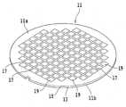
도 1은 광 디바이스 웨이퍼의 표면측 사시도.
도 2는 경사면 설정 단계를 설명하는 광 디바이스 웨이퍼의 단면도.
도 3은 광 디바이스 웨이퍼 유지 단계를 도시하는 사시도.
도 4는 레이저 가공 단계를 설명하는 사시도.
도 5는 레이저빔 조사 유닛의 블록도.
도 6은 레이저 가공 단계를 도시하는 광 디바이스 웨이퍼의 단면도.
도 7은 분할 단계를 도시하는 광 디바이스 웨이퍼의 단면도.
도 8은 개질층 형성 단계를 도시하는 광 디바이스 웨이퍼의 단면도.
도 9는 분할 단계를 도시하는 광 디바이스 웨이퍼의 단면도.
도 10은 본 발명의 제1 실시형태의 광 디바이스의 사시도.
도 11의 (A)는 도 10의 선 11A-11A를 따라 취한 단면도, 도 11의 (B)는 도 10의 선 11B-11B를 따라 취한 단면도.
도 12는 본 발명의 제2 실시형태의 광 디바이스의 사시도.
도 13의 (A)는 도 12의 선 13A-13A를 따라 취한 단면도, 도 13의 (B)는 도 12의 선 13B-13B를 따라 취한 단면도.
도 14의 (A)는 역사다리꼴형의 광 디바이스의 제1 절단선을 따른 단면도, 도 14의 (B)는 제1 절단선에 직교하는 제2 절단선을 따른 단면도.
도 15는 또 다른 실시형태의 광 디바이스의 단면도.1 is a front side perspective view of an optical device wafer.
2 is a cross-sectional view of an optical device wafer illustrating a slope setting step;
3 is a perspective view showing an optical device wafer holding step;
4 is a perspective view illustrating a laser processing step;
5 is a block diagram of a laser beam irradiation unit.
6 is a cross-sectional view of an optical device wafer showing a laser processing step;
7 is a cross-sectional view of an optical device wafer showing the splitting step;
8 is a cross-sectional view of an optical device wafer showing a modified layer forming step.
9 is a cross-sectional view of an optical device wafer showing the splitting step.
10 is a perspective view of an optical device according to the first embodiment of the present invention.
FIG. 11A is a cross-sectional view taken along
12 is a perspective view of an optical device according to a second embodiment of the present invention;
FIG. 13A is a cross-sectional view taken along the
Fig. 14A is a cross-sectional view of an inverted trapezoidal optical device along a first cutting line, and Fig. 14B is a cross-sectional view taken along a second cutting line perpendicular to the first cutting line. Fig.
15 is a cross-sectional view of an optical device according to still another embodiment;
이하, 본 발명의 실시형태를 도면을 참조하여 상세히 설명한다. 도 1을 참조하면, 광 디바이스 웨이퍼(11)의 표면측 사시도가 도시되어 있다. 광 디바이스 웨이퍼(11)는, 사파이어 기판(13)상에 질화갈륨(GaN) 등의 발광층(에피택셜층)(15)이 적층되어 구성되어 있다. 광 디바이스 웨이퍼(11)는, 발광층(15)이 적층된 표면(11a)과, 사파이어 기판(13)이 노출된 이면(11b)을 갖고 있다.BEST MODE FOR CARRYING OUT THE INVENTION Hereinafter, embodiments of the present invention will be described in detail with reference to the drawings. Referring to Fig. 1, a front side perspective view of an
사파이어 기판(13)은 예컨대 100 ㎛의 두께를 갖고 있고, 발광층(15)은 예컨대 5 ㎛의 두께를 갖고 있다. 발광층(15)에 LED 등의 복수의 광 디바이스(19)가 격자형으로 설정된 분할 예정 라인(스트리트)(17)에 의해 구획되어 형성되어 있다.The
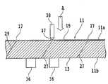
본 발명의 광 디바이스의 가공 방법에서는, 전술한 바와 같은 광 디바이스 웨이퍼(11)를 준비한 후, 광 디바이스 웨이퍼(11)에, 형성해야 하는 광 디바이스의 측면의 경사 각도에 대응한 복수의 경사면을 설정하는 경사면 설정 단계를 실시한다.In the method of processing an optical device of the present invention, after the optical device wafer 11 as described above is prepared, a plurality of inclined surfaces corresponding to the inclination angles of the side surfaces of the optical device to be formed are set on the optical device wafer 11 A slope setting step is performed.
이 경사면 설정 단계에서는, 도 2에 도시하는 바와 같이, 형성해야 하는 광 디바이스(19)의 측면의 경사 각도와 광 디바이스 웨이퍼(11)의 두께로부터, 분할 예정 라인(17)의 중심(17a)으로부터 이면(11b)을 향해 정해진 각도의 경사면(21)을 그었을 때의 경사면(21)과 이면(11b)의 교점 위치(23)를 레이저빔 조사 라인으로서 설정한다.2, from the inclination angle of the side surface of the
그리고, 레이저빔 조사 라인(23)이 분할 예정 라인(17)의 신장 방향에 직교하는 방향으로 분할 예정 라인(17)의 중심(17a)으로부터 어느 정도 어긋나 있는지를 산출한다. 또한, 이 어긋남의 거리를 이하 오프셋 거리로 칭한다. 오프셋 거리는, 광 디바이스 웨이퍼(11)의 분할 예정 라인(17)의 중심간 거리(인덱스량)와 함께 레이저 가공 장치(8)의 메모리에 기억된다.It is calculated how far the laser
경사면 설정 단계를 실시한 후, 도 3에 도시하는 바와 같이, 레이저 가공 장치(8)의 척 테이블(10)에서 다이싱 테이프(T)를 개재하여 광 디바이스 웨이퍼(11)를 흡인 유지하고, 광 디바이스 웨이퍼(11)의 이면(11b)을 노출시킨다. 그리고, 다이싱 테이프(T)의 외주부가 접착된 환형 프레임(F)을 도시를 생략한 클램프로 클램프하여 고정한다.The
레이저빔 조사 유닛(12)은, 케이싱(16) 안에 수용된 도 5에 도시하는 레이저빔 발생 유닛(18)과, 케이싱(16)의 선단부에 회동 가능하게 부착된 집광기(레이저 헤드)(20)로 구성된다.The laser
34는 현미경 및 CCD 카메라 등의 통상의 촬상 소자, 더 나아가서는 적외선 촬상 소자를 갖는 촬상 유닛이다. 광 디바이스 웨이퍼(11)는 사파이어 기판(13)상에 발광층(15)이 적층되어 구성되어 있고, 사파이어 기판(13)이 투명하기 때문에 통상의 촬상 소자로 광 디바이스 웨이퍼(11)의 이면(11b)측으로부터 표면(11a)에 형성된 분할 예정 라인(17)을 촬상할 수 있다.
본 발명의 광 디바이스의 가공 방법에서는, 촬상 유닛(34)으로 광 디바이스 웨이퍼(11)를 그 이면(11b)측으로부터 촬상하고, 분할 예정 라인(17)과 집광기(레이저 헤드)(20)를 X축 방향으로 정렬시키는 얼라인먼트를 실시한다.In the optical device processing method of the present invention, the
이 얼라인먼트 단계에서는, 광 디바이스 웨이퍼(11)의 분할 예정 라인(17)을 레이저 가공 장치(8)의 집광기(20)와 X축 방향으로 정렬시켜, 제1 방향으로 연장하는 분할 예정 라인(17)을 검출하여 그 Y 좌표값을 메모리에 저장한 후, 척 테이블(10)을 90도 회전시킨 후, 제1 방향에 직교하는 제2 방향으로 연장하는 분할 예정 라인(17)을 검출하여, 그 Y 좌표값을 메모리에 저장한다.In this alignment step, the line to be divided 17 of the
얼라인먼트를 실시한 후, 광 디바이스 웨이퍼(11)에 대하여 흡수성을 갖는 파장의 레이저빔을 분할 예정 라인(17)으로부터 오프셋 거리만큼 떨어진 위치의 웨이퍼 이면(11b)의 레이저빔 조사 라인(23)을 따라, 그리고 경사면(27)을 따라 조사하여, 경사면(21)을 따른 레이저 가공 홈(27)을 형성하는 레이저 가공 단계를 실시한다.After the alignment, the laser beam of a wavelength having an absorbing property is applied to the optical device wafer 11 along the laser
레이저빔 조사 유닛(12)의 레이저빔 발생 유닛(18)은, 도 5에 도시하는 바와 같이, YAG 레이저 또는 YVO4 레이저를 발진하는 레이저 발진기(22)와, 반복 주파수 설정 수단(24)과, 펄스폭 조정 수단(26)과, 파워 조정 수단(28)을 포함하고 있다.5, the laser
레이저빔 발생 유닛(18)의 파워 조정 수단(28)에 의해 정해진 파워로 조정된 펄스 레이저빔은, 케이싱(16)의 선단에 회동 가능하게 부착된 집광기(20)의 미러(30)로 반사되고, 또한 집광용 대물 렌즈(32)에 의해 집광되어 척 테이블(10)에 유지되어 있는 광 디바이스 웨이퍼(11)에 조사된다.The pulsed laser beam adjusted to the power determined by the power adjusting means 28 of the laser
이 레이저 가공 단계를 실시할 때에는, 도 6에 도시하는 바와 같이, 집광기(20)를 경사면(21)과 평행하게 될 때까지 회동하고, 집광기(20)로부터 정해진 파워로 조정된 펄스 레이저빔을 광 디바이스 웨이퍼(11)의 이면(11b)에 조사하여, 경사면(21)을 따라 정해진 깊이의 레이저 가공 홈(27)을 형성한다.6, the
척 테이블(10)을 Y축 방향으로 인덱스량만큼 인덱싱 이송하면서, 제1 방향으로 연장하는 모든 분할 예정 라인(17)에 대응하여 경사면(21)을 따른 레이저 가공 홈(27)을 형성한다. 이어서, 척 테이블(10)을 90도 회전시킨 후, 제1 방향에 직교하는 제2 방향으로 연장하는 모든 분할 예정 라인(17)에 대응하여 경사면(21)을 따른 레이저 가공 홈(27)을 형성한다.The
이 레이저 가공 단계의 가공 조건은, 예컨대 다음과 같이 설정되어 있다.The processing conditions of this laser processing step are set, for example, as follows.
광원 : LD 여기 Q 스위치 Nd: YAG 레이저Light source: LD excitation Q switch Nd: YAG laser
파장 : 355 ㎚(YAG 레이저의 제3 고조파)Wavelength: 355 nm (third harmonic of YAG laser)
평균 출력 : 2 WAverage power: 2 W
가공 이송 속도: 100 ㎜/초Processing feed rate: 100 mm / sec
레이저 가공 단계를 실시한 후, 광 디바이스 웨이퍼(11)에 외력을 부여하여 광 디바이스 웨이퍼(11)를 개개의 광 디바이스로 분할하는 분할 단계를 실시한다. 이 분할 단계에서는, 예컨대 도 7에 도시하는 바와 같이, 정해진 간격 이격된 한 쌍의 지지대(36) 사이에 경사진 레이저 가공 홈(27)이 위치하도록 광 디바이스 웨이퍼(11)의 이면(11b)을 지지대(36)상에 위치시켜 탑재한다.After the laser processing step is performed, an external force is applied to the
그리고, 예각 선단부를 갖는 쐐기형의 분할 바(38)를 화살표 A 방향으로 이동시켜, 광 디바이스 웨이퍼(11)의 표면(11a)에 형성된 분할 예정 라인(17)에 분할 바(38)를 압박하는 것에 의해, 레이저 가공 홈(27)을 분할 기점으로 하여 광 디바이스 웨이퍼(11)를 부호 29로 나타내는 바와 같이 할단한다. 분할 바(38)의 구동은, 예컨대 에어 실린더 등에 의해 행한다.The wedge-shaped
한쪽 레이저 가공 홈(27)을 따른 할단이 종료하면, 광 디바이스 웨이퍼(11)를 가로 방향으로 1피치분 이동시켜, 다음의 레이저 가공 홈(27)을 한 쌍의 지지대(36)의 중간 부분에 위치시키고, 분할 바(38)를 구동하여 다음의 레이저 가공 홈(27)을 분할 기점으로 하여 광 디바이스 웨이퍼(11)를 할단한다.The
제1 방향으로 연장하는 모든 분할 예정 라인(17)을 따른 분할이 종료하면, 광 디바이스 웨이퍼(11)를 90도 회전시켜, 제1 방향으로 연장하는 분할 예정 라인(17)에 직교하는 제2 방향으로 연장하는 분할 예정 라인(17)을 따라 마찬가지로 분할한다. 이것에 의해, 광 디바이스 웨이퍼(11)가 개개의 광 디바이스 칩으로 분할된다.The
전술한 설명에서는, 한 쌍의 지지대(36) 및 분할 바(38)가 가로 방향으로 고정되고, 광 디바이스 웨이퍼(11)가 가로 방향으로 이동하는 것으로 했지만, 광 디바이스 웨이퍼(11)를 정지 상태로 유지하고, 지지대(36) 및 분할 바(38)를 가로 방향으로 1피치씩 이동시키도록 하여도 좋다.In the above description, the pair of
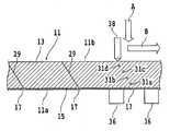
다음에, 도 8을 참조하여, 본 발명의 제2 실시형태의 레이저 가공 단계인 개질층 형성 단계에 대해서 설명한다. 이 개질층 형성 단계에서는, 우선 도 8의 (A)에 도시하는 바와 같이, 레이저빔의 집광점을 경사면(21)상의 표면(11a) 근방에 위치시키고, 광 디바이스 웨이퍼(11)의 이면(11b)측으로부터 광 디바이스 웨이퍼(11)에 대하여 투과성을 갖는 파장의 레이저빔을 제1 방향으로 연장하는 분할 예정 라인(17)으로부터 Y축 방향으로 정해진 거리 떨어져 조사하여, 광 디바이스 웨이퍼(11)의 내부에 제1 개질층(31a)을 형성한다.Next, with reference to Fig. 8, the modified layer forming step which is the laser processing step of the second embodiment of the present invention will be described. 8A, the light-converging point of the laser beam is positioned in the vicinity of the
이어서, 도 8의 (B)에 도시하는 바와 같이, 레이저빔의 집광점을 서서히 이면(11b)측으로 이동시켜, 경사면(21)을 따른 제2 개질층(31b), 제3 개질층(31c), 제4 개질층(31d)을 형성한다.8B, the light condensing point of the laser beam is gradually moved to the
이어서, 척 테이블(10)을 Y축 방향으로 1피치 인덱싱 이송하여, 다음의 분할 예정 라인(17)에 대응하는 경사면(21)을 따라 같은 제1 내지 제4 개질층(31a∼31d)을 형성한다.Subsequently, the chuck table 10 is indexed by one pitch in the Y-axis direction to form the same first to fourth modified
개질층을 형성하는 레이저 가공 조건은, 예컨대 다음과 같이 설정되어 있다.The laser processing conditions for forming the modified layer are set as follows, for example.
광원 : LD 여기 Q 스위치 Nd: YAG 레이저Light source: LD excitation Q switch Nd: YAG laser
파장 : 1064 ㎚Wavelength: 1064 nm
평균 출력 : 0.1 W∼0.2 WAverage output: 0.1 W to 0.2 W
가공 이송 속도 : 600 ㎜/초Feeding speed: 600 mm / sec
모든 분할 예정 라인(17)에 대응하는 경사면(21)을 따라 개질층 형성 단계를 실시한 후, 도 9에 도시하는 바와 같이, 정해진 간격 이격된 한 쌍의 지지대(36) 사이에 제1 개질층(31a)이 위치하도록 광 디바이스 웨이퍼(11)를 지지대(36)상에 위치시켜 탑재하고, 예각 선단부를 갖는 쐐기형의 분할 바(38)를 화살표 A 방향으로 이동시켜, 광 디바이스 웨이퍼(11)의 이면(11b)에 분할 바(38)를 압박하는 것에 의해, 개질층(31a∼31d)을 분할 기점으로 하여 광 디바이스 웨이퍼(11)를 부호 29로 나타내는 바와 같이 할단한다.After the modified layer forming step is performed along the
개질층(31a∼31d)을 갖는 일체의 경사면(21)을 따른 할단이 종료하면, 광 디바이스 웨이퍼(11)를 화살표 B 방향으로 1피치분 이동시켜, 다음의 제1 개질층(31a)을 한 쌍의 지지대(36)의 중간 부분에 위치시키고, 분할 바(38)를 구동하여 다음의 개질층(31a∼31d)을 분할 기점으로 하여 광 디바이스 웨이퍼(11)를 할단한다.The
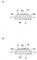
도 10을 참조하면, 전술한 실시형태의 광 디바이스의 가공 방법에 의해 형성된 제1 실시형태의 LED 등의 광 디바이스(33)의 사시도가 도시되어 있다. 광 디바이스(33)는, 사파이어 기판(13)상에 발광층(15)이 적층되어 구성되어 있다. 도 11의 (A)는 도 10의 11A-11A를 따라 취한 단면도이고, 도 11의 (B)는 도 10의 11B-11B를 따라 취한 단면도이다.Referring to Fig. 10, there is shown a perspective view of an
광 디바이스(33)는, 발광층(15)을 갖는 사각형의 표면(33a)과, 사파이어 기판(13)이 노출된 사각형의 이면(33b)과, 표면(33a)과 이면(33b)을 연결하는 제1 내지 제4 측면(33c∼33f)을 갖고 있다. 이면(33b)은 표면(33a)에 대략 평행하다.The
도 11의 (A)에 도시하는 바와 같이, 제1 측면(33c)은 표면(33a)의 수직선에 대하여 제1 각도(θ1) 경사지고, 제1 측면(33c)에 대면하는 제2 측면(33d)은 표면(33a)의 수직선에 대하여 제2 각도(θ2)로 경사져 있다.11A, the
또한, 도 11의 (B)에 도시하는 바와 같이, 제3 측면(33e)은 표면(33a)의 수직선에 대하여 제3 각도(θ3) 경사지고, 제3 측면(33e)에 대면하는 제4 측면(33f)은 표면(33a)의 수직선에 대하여 제4 각도(θ4) 경사져 있다.11 (B), the
예컨대, 본 실시형태의 광 디바이스(33)는, 제1 각도(θ1) 내지 제4 각도(θ4)가 모두 동일 각도이고, 이 경우에는, 광 디바이스(33)의 표면(33a)으로부터 이면(33b)에 이르는 단면 형상(종단면 형상)이 평행사변형이 된다. 예컨대 θ1∼θ4는 30도로 설정된다. θ1∼θ4를 각각 상이한 각도로 설정하도록 하여도 좋다.For example, in the
도 12를 참조하면, 본 발명의 제2 실시형태의 광 디바이스(35)의 사시도가 도시되어 있다. 도 13의 (A)는 도 12의 선 13A-13A를 따라 취한 단면도를 도시하고, 도 13의 (B)는 도 12의 선 13B-13B를 따라 취한 단면도를 각각 도시하고 있다.Referring to Fig. 12, there is shown a perspective view of an
광 디바이스(35)는, 발광층(15)을 갖는 사각형의 표면(35a)과, 표면(35a)과 대략 평행하게 형성되고 사파이어 기판(13)이 노출된 사각형의 이면(35b)과, 표면(35a)과 이면(35b)을 연결하는 제1 내지 제4 측면(35c∼35f)을 갖고 있다.The
도 13의 (A)에 도시하는 바와 같이, 제1 측면(35c)은 표면(35a)의 수직선에 대하여 제1 각도(θ1) 경사지고, 제1 측면(35c)에 대면하는 제2 측면(35b)은 표면(35a)의 수직선에 대하여 제2 각도(θ2)로 경사져 있다.13A, the
또한 도 13의 (B)에 도시하는 바와 같이, 제3 측면(35e)은 표면(35a)의 수직선에 대하여 제3 각도(θ3) 경사지고, 제3 측면(35e)에 대면하는 제4 측면(35f)은 표면(35a)의 수직선에 대하여 제4 각도(θ4) 경사져 있다.13B, the
여기서, 제1 각도 내지 제4 각도(θ1∼θ4)가 모두 동일 각도인 경우에는, 광 디바이스(35)의 종단면 형상[표면(35a)으로부터 이면(35b)에 이르는 단면 형상]은 사다리꼴이 된다. 제1 각도 내지 제4 각도(θ1∼θ4)를 모두 상이한 각도로 설정하도록 하여도 좋다.Here, when the first to fourth angles? 1 to? 4 are all at the same angle, the longitudinal shape of the optical device 35 (the cross-sectional shape from the
도 14를 참조하면, 본 발명의 제3 실시형태의 광 디바이스(37)의 종단면도가 도시되어 있다. 본 실시형태의 광 디바이스(37)는, 발광층을 갖는 사각형의 표면(37a)과, 표면(37a)에 대략 평행하고 사파이어 기판(13)이 노출된 사각형의 이면(37b)과, 표면(37a)과 이면(37b)을 연결하는 제1 내지 제4 측면(37c∼37f)을 갖고 있다.Referring to Fig. 14, a longitudinal sectional view of an
도 14의 (A)에 도시하는 바와 같이, 제1 측면(37c)은 표면(37a)의 수직선에 대하여 제1 각도(θ1) 경사지고, 제1 측면(37c)에 대면하는 제2 측면(37b)은 표면(37a)의 수직선에 대하여 제2 각도(θ2) 경사져 있다.14A, the
또한 도 14의 (B)에 도시하는 바와 같이, 제3 측면(37e)은 표면(37a)의 수직선에 대하여 제3 각도(θ3) 경사지고, 제3 측면(37e)에 대면하는 제4 측면(37f)은 표면(37a)의 수직선에 대하여 제4 각도(θ4) 경사져 있다.14B, the third side surface 37e is inclined at a third angle? 3 with respect to the vertical line of the
제1 각도 내지 제4 각도(θ1∼θ4)가 모두 동일 각도인 경우에는, 광 디바이스(37)의 종단면 형상은 역사다리꼴이 된다. 물론, 제1 각도 내지 제4 각도(θ1∼θ4)를 각각 상이한 각도로 설정하도록 하여도 좋다.When the first to fourth angles? 1 to? 4 are all at the same angle, the longitudinal shape of the
도 15를 참조하면, 본 발명의 제4 실시형태의 광 디바이스(39)의 종단면도가 도시되어 있다. 광 디바이스(39)는, 발광층(15)을 갖는 사각형의 표면(39a)과, 표면(39a)에 대략 평행하고 사파이어 기판(13)이 노출된 사각형의 이면(39b)과, 표면(39a)과 이면(39b)을 연결하는 4측면을 갖고 있다.Referring to Fig. 15, there is shown a longitudinal sectional view of an
도 15로부터 명백한 바와 같이, 제1 측면(39c)은 표면(39a)의 수직선에 대하여 제1 각도(θ1) 경사지고, 제1 측면(39c)에 대면하는 제2 측면(39b)은 표면(39a)의 수직선에 대하여 제1 각도(θ1)와는 상이한 제2 각도(θ2) 경사져 있다. 제3 측면과 제4 측면은 도시되어 있지 않지만, 제3 측면을 제3 각도(θ3) 경사지게 하고, 제4 측면을 제3 각도(θ3)와는 상이한 제4 각도(θ4) 경사지게 하여도 좋다.15, the
11: 광 디바이스 웨이퍼, 12: 레이저빔 조사 유닛, 13: 사파이어 기판, 15: 발광층(에피택셜층), 17: 분할 예정 라인, 18: 레이저빔 발생 유닛, 19: 광 디바이스, 20: 레이저빔 발생 유닛, 21: 경사면, 23: 레이저빔 조사 라인, 27: 레이저 가공 홈, 33, 35, 37, 39: 광 디바이스, 36: 지지대, 38: 분할 바(11): optical device wafer (12): laser beam irradiation unit (13): sapphire substrate (15): light emitting layer (epitaxial layer) 27 is a perspective view of a laser beam processing apparatus according to the present invention;
Claims (6)
Translated fromKorean발광층을 갖는 사각형의 표면과, 상기 표면과 평행한 사각형의 이면과, 상기 표면과 상기 이면을 연결하는 제1 내지 제4 측면을 가지며,
제1 측면은 상기 표면의 수직선으로부터 제1 각도 경사지고, 상기 제1 측면에 대면하는 제2 측면은 상기 수직선으로부터 제2 각도 경사지며, 제3 측면은 상기 수직선으로부터 제3 각도 경사지고, 상기 제3 측면에 대면하는 제4 측면은 상기 수직선으로부터 제4 각도 경사지는 것을 특징으로 하는 광 디바이스.As an optical device,
A quadrangular surface having a light emitting layer, a quadrangular surface parallel to the surface, and first to fourth surfaces connecting the surface and the back surface,
The first side is inclined by a first angle from the vertical line of the surface, the second side facing the first side is inclined by the second angle from the vertical line, the third side is inclined by the third angle from the vertical line, And the fourth side facing the third side is inclined at a fourth angle from the vertical line.
표면에 발광층을 갖고, 복수의 교차하는 분할 예정 라인이 설정되며, 상기 분할 예정 라인으로 구획된 상기 발광층의 각 영역에 각각 광 디바이스를 갖는 광 디바이스 웨이퍼를 준비하는 웨이퍼 준비 단계와,
광 디바이스 웨이퍼에 상기 광 디바이스의 상기 제1 내지 제4 측면에 대응한 복수의 경사면을 설정하는 경사면 설정 단계와,
상기 경사면 설정 단계를 실시한 후, 광 디바이스 웨이퍼에 대하여 흡수성을 갖는 파장의 레이저빔을 상기 경사면을 따라 조사하여 상기 경사면을 따른 레이저 가공 홈을 형성하는 레이저 가공 단계
를 포함하는 것을 특징으로 하는 광 디바이스의 가공 방법.A method of processing an optical device according to claim 1,
A wafer preparation step of preparing an optical device wafer having a light emitting layer on its surface and a plurality of intersecting dividing lines to be set and each having an optical device in each region of the light emitting layer partitioned by the line to be divided,
A slope setting step of setting a plurality of slopes corresponding to the first to fourth sides of the optical device on an optical device wafer,
A laser processing step of forming a laser processing groove along the inclined surface by irradiating the optical device wafer along the inclined surface with a laser beam having an absorbing wavelength after performing the inclined plane setting step,
The method comprising the steps of:
Applications Claiming Priority (2)
| Application Number | Priority Date | Filing Date | Title |
|---|---|---|---|
| JPJP-P-2012-155265 | 2012-07-11 | ||
| JP2012155265AJP5995563B2 (en) | 2012-07-11 | 2012-07-11 | Optical device processing method |
Publications (2)
| Publication Number | Publication Date |
|---|---|
| KR20140008497Atrue KR20140008497A (en) | 2014-01-21 |
| KR101939409B1 KR101939409B1 (en) | 2019-01-16 |
Family
ID=49913220
Family Applications (1)
| Application Number | Title | Priority Date | Filing Date |
|---|---|---|---|
| KR1020130072819AActiveKR101939409B1 (en) | 2012-07-11 | 2013-06-25 | Optical device and method for machining optical device |
Country Status (5)
| Country | Link |
|---|---|
| US (1) | US20140014976A1 (en) |
| JP (1) | JP5995563B2 (en) |
| KR (1) | KR101939409B1 (en) |
| CN (1) | CN103545409B (en) |
| TW (1) | TWI578561B (en) |
Cited By (2)
| Publication number | Priority date | Publication date | Assignee | Title |
|---|---|---|---|---|
| KR20160108183A (en)* | 2015-03-05 | 2016-09-19 | 가부시기가이샤 디스코 | Method of manufacturing device chips |
| KR20180056381A (en)* | 2016-11-18 | 2018-05-28 | 가부시기가이샤 디스코 | Method of manufacturing device chip package |
Families Citing this family (13)
| Publication number | Priority date | Publication date | Assignee | Title |
|---|---|---|---|---|
| JP2015138815A (en)* | 2014-01-21 | 2015-07-30 | 株式会社ディスコ | Optical device and method of processing optical device |
| US10353453B2 (en)* | 2014-02-25 | 2019-07-16 | Dell Products L.P. | Methods and systems for multiple module power regulation in a modular chassis |
| JP6301726B2 (en)* | 2014-05-07 | 2018-03-28 | 株式会社ディスコ | Optical device processing method |
| JP2016054205A (en)* | 2014-09-03 | 2016-04-14 | 株式会社ディスコ | Wafer processing method |
| JP2016111119A (en)* | 2014-12-04 | 2016-06-20 | 株式会社ディスコ | Processing method of optical device |
| JP6407066B2 (en)* | 2015-03-06 | 2018-10-17 | 株式会社ディスコ | Manufacturing method of optical device chip |
| JP7277782B2 (en)* | 2019-12-27 | 2023-05-19 | 日亜化学工業株式会社 | Semiconductor device manufacturing method |
| JP7453013B2 (en)* | 2020-02-14 | 2024-03-19 | 株式会社ディスコ | Wafer processing method |
| CN111267248A (en)* | 2020-03-12 | 2020-06-12 | 常州时创能源股份有限公司 | Preparation method of non-100 crystal orientation monocrystalline silicon wafer |
| KR20230037546A (en)* | 2020-07-15 | 2023-03-16 | 하마마츠 포토닉스 가부시키가이샤 | Laser processing device, laser processing method, and method of manufacturing a semiconductor member |
| CN116113517A (en)* | 2020-07-15 | 2023-05-12 | 浜松光子学株式会社 | Laser processing device and laser processing method |
| CN116075389A (en)* | 2020-07-15 | 2023-05-05 | 浜松光子学株式会社 | Laser processing device and laser processing method |
| CN117430339A (en)* | 2023-10-10 | 2024-01-23 | 南方科技大学 | Glass micro groove processing method and system and glass product |
Citations (7)
| Publication number | Priority date | Publication date | Assignee | Title |
|---|---|---|---|---|
| US3824678A (en)* | 1970-08-31 | 1974-07-23 | North American Rockwell | Process for laser scribing beam lead semiconductor wafers |
| JPH10305420A (en) | 1997-03-04 | 1998-11-17 | Ngk Insulators Ltd | Processing method of base material composed of oxide single crystal and method of manufacturing functional device |
| US20010000209A1 (en)* | 1997-06-03 | 2001-04-12 | Krames Michael R. | Led having angled sides for increased side light extraction |
| US6515309B1 (en)* | 1998-12-25 | 2003-02-04 | Oki Electric Industry Co., Ltd. | LED array chip |
| JP2003298107A (en)* | 2002-01-29 | 2003-10-17 | Toshiba Corp | Semiconductor light emitting device and method of manufacturing the same |
| JP2008006492A (en) | 2006-06-30 | 2008-01-17 | Disco Abrasive Syst Ltd | Processing method of sapphire substrate |
| JP2009124077A (en)* | 2007-11-19 | 2009-06-04 | Denso Corp | Semiconductor chip and its production process |
Family Cites Families (13)
| Publication number | Priority date | Publication date | Assignee | Title |
|---|---|---|---|---|
| US5151389A (en)* | 1990-09-10 | 1992-09-29 | Rockwell International Corporation | Method for dicing semiconductor substrates using an excimer laser beam |
| US20050263854A1 (en)* | 1998-10-23 | 2005-12-01 | Shelton Bryan S | Thick laser-scribed GaN-on-sapphire optoelectronic devices |
| DE10032838B4 (en)* | 2000-07-06 | 2015-08-20 | Osram Opto Semiconductors Gmbh | Radiation emitting semiconductor chip and method for its production |
| JP3776824B2 (en)* | 2002-04-05 | 2006-05-17 | 株式会社東芝 | Semiconductor light emitting device and manufacturing method thereof |
| US20040169185A1 (en)* | 2003-02-28 | 2004-09-02 | Heng Liu | High luminescent light emitting diode |
| US20050029646A1 (en)* | 2003-08-07 | 2005-02-10 | Matsushita Electric Industrial Co., Ltd. | Semiconductor device and method for dividing substrate |
| JP4408361B2 (en)* | 2003-09-26 | 2010-02-03 | 株式会社ディスコ | Wafer division method |
| KR100627006B1 (en)* | 2004-04-01 | 2006-09-25 | 삼성전자주식회사 | Indent chips, semiconductor packages and multi-chip packages using the same |
| JP4471852B2 (en)* | 2005-01-21 | 2010-06-02 | パナソニック株式会社 | Semiconductor wafer, manufacturing method using the same, and semiconductor device |
| US7611966B2 (en)* | 2005-05-05 | 2009-11-03 | Intel Corporation | Dual pulsed beam laser micromachining method |
| JP2007019262A (en)* | 2005-07-07 | 2007-01-25 | Toshiba Discrete Technology Kk | Semiconductor light emitting device and method for manufacturing semiconductor light emitting device |
| JP5671982B2 (en)* | 2010-11-30 | 2015-02-18 | 三菱化学株式会社 | Semiconductor light emitting device and method for manufacturing semiconductor light emitting device |
| CN102270717B (en)* | 2011-07-15 | 2013-03-06 | 华灿光电股份有限公司 | Light emitting diode chip with curved substrate side surface and manufacture method thereof |
- 2012
- 2012-07-11JPJP2012155265Apatent/JP5995563B2/enactiveActive
- 2013
- 2013-05-21TWTW102117880Apatent/TWI578561B/enactive
- 2013-06-25KRKR1020130072819Apatent/KR101939409B1/enactiveActive
- 2013-07-09USUS13/937,976patent/US20140014976A1/ennot_activeAbandoned
- 2013-07-10CNCN201310287638.3Apatent/CN103545409B/enactiveActive
Patent Citations (7)
| Publication number | Priority date | Publication date | Assignee | Title |
|---|---|---|---|---|
| US3824678A (en)* | 1970-08-31 | 1974-07-23 | North American Rockwell | Process for laser scribing beam lead semiconductor wafers |
| JPH10305420A (en) | 1997-03-04 | 1998-11-17 | Ngk Insulators Ltd | Processing method of base material composed of oxide single crystal and method of manufacturing functional device |
| US20010000209A1 (en)* | 1997-06-03 | 2001-04-12 | Krames Michael R. | Led having angled sides for increased side light extraction |
| US6515309B1 (en)* | 1998-12-25 | 2003-02-04 | Oki Electric Industry Co., Ltd. | LED array chip |
| JP2003298107A (en)* | 2002-01-29 | 2003-10-17 | Toshiba Corp | Semiconductor light emitting device and method of manufacturing the same |
| JP2008006492A (en) | 2006-06-30 | 2008-01-17 | Disco Abrasive Syst Ltd | Processing method of sapphire substrate |
| JP2009124077A (en)* | 2007-11-19 | 2009-06-04 | Denso Corp | Semiconductor chip and its production process |
Cited By (2)
| Publication number | Priority date | Publication date | Assignee | Title |
|---|---|---|---|---|
| KR20160108183A (en)* | 2015-03-05 | 2016-09-19 | 가부시기가이샤 디스코 | Method of manufacturing device chips |
| KR20180056381A (en)* | 2016-11-18 | 2018-05-28 | 가부시기가이샤 디스코 | Method of manufacturing device chip package |
Also Published As
| Publication number | Publication date |
|---|---|
| KR101939409B1 (en) | 2019-01-16 |
| TW201403855A (en) | 2014-01-16 |
| US20140014976A1 (en) | 2014-01-16 |
| JP5995563B2 (en) | 2016-09-21 |
| TWI578561B (en) | 2017-04-11 |
| CN103545409B (en) | 2019-01-01 |
| JP2014017433A (en) | 2014-01-30 |
| CN103545409A (en) | 2014-01-29 |
Similar Documents
| Publication | Publication Date | Title |
|---|---|---|
| KR101939409B1 (en) | Optical device and method for machining optical device | |
| KR101752016B1 (en) | Method for dividing optical device wafer | |
| KR102361277B1 (en) | Wafer producing method | |
| KR102341602B1 (en) | Wafer producing method | |
| KR102361278B1 (en) | Wafer producing method | |
| JP5439331B2 (en) | Method of dividing the object to be divided | |
| KR101854679B1 (en) | Laser processing apparatus and method for setting processing condition of substrate with pattern | |
| JP5770436B2 (en) | Laser processing apparatus and laser processing method | |
| JP6345742B2 (en) | Substrate processing method | |
| WO2013176089A1 (en) | Cutting method for item to be processed, item to be processed and semiconductor element | |
| KR20110047131A (en) | Laser processing method, method of dividing the workpiece and laser processing device | |
| KR20160067779A (en) | Method for processing optical device | |
| JP2006245043A (en) | Method of manufacturing group iii nitride-based compound semiconductor element, and light emitting element | |
| KR20150103631A (en) | Optical device | |
| KR20180119482A (en) | Wafer processing method | |
| CN108461396B (en) | Processing method of optical device wafer | |
| KR101889385B1 (en) | Method for processing substrate with pattern | |
| CN108093626A (en) | Laser processing and laser processing device | |
| JP5318545B2 (en) | Wafer processing method | |
| KR20200010042A (en) | Method for processing led wafer | |
| JP2013235877A (en) | Optical device wafer processing method | |
| TW201440935A (en) | Processing method and processing device of patterned substrate | |
| US8945963B2 (en) | Optical device processing method |
Legal Events
| Date | Code | Title | Description |
|---|---|---|---|
| PA0109 | Patent application | Patent event code:PA01091R01D Comment text:Patent Application Patent event date:20130625 | |
| PG1501 | Laying open of application | ||
| PA0201 | Request for examination | Patent event code:PA02012R01D Patent event date:20170623 Comment text:Request for Examination of Application Patent event code:PA02011R01I Patent event date:20130625 Comment text:Patent Application | |
| E902 | Notification of reason for refusal | ||
| PE0902 | Notice of grounds for rejection | Comment text:Notification of reason for refusal Patent event date:20180620 Patent event code:PE09021S01D | |
| E701 | Decision to grant or registration of patent right | ||
| PE0701 | Decision of registration | Patent event code:PE07011S01D Comment text:Decision to Grant Registration Patent event date:20181011 | |
| GRNT | Written decision to grant | ||
| PR0701 | Registration of establishment | Comment text:Registration of Establishment Patent event date:20190110 Patent event code:PR07011E01D | |
| PR1002 | Payment of registration fee | Payment date:20190110 End annual number:3 Start annual number:1 | |
| PG1601 | Publication of registration | ||
| PR1001 | Payment of annual fee | Payment date:20211222 Start annual number:4 End annual number:4 | |
| PR1001 | Payment of annual fee | Payment date:20241218 Start annual number:7 End annual number:7 |