KR20140001145A - Body-contacted partially depleted silicon on insulator transistor - Google Patents
Body-contacted partially depleted silicon on insulator transistorDownload PDFInfo
- Publication number
- KR20140001145A KR20140001145AKR1020130073469AKR20130073469AKR20140001145AKR 20140001145 AKR20140001145 AKR 20140001145AKR 1020130073469 AKR1020130073469 AKR 1020130073469AKR 20130073469 AKR20130073469 AKR 20130073469AKR 20140001145 AKR20140001145 AKR 20140001145A
- Authority
- KR
- South Korea
- Prior art keywords
- transistor
- contact
- circuit
- switch
- resistor
- Prior art date
- Legal status (The legal status is an assumption and is not a legal conclusion. Google has not performed a legal analysis and makes no representation as to the accuracy of the status listed.)
- Abandoned
Links
- 229910052710siliconInorganic materials0.000titleclaimsabstractdescription11
- 239000010703siliconSubstances0.000titleclaimsabstractdescription11
- 239000012212insulatorSubstances0.000titleclaimsabstractdescription8
- 238000000034methodMethods0.000claimsabstractdescription23
- 230000003321amplificationEffects0.000claimsdescription5
- 238000003199nucleic acid amplification methodMethods0.000claimsdescription5
- 230000005540biological transmissionEffects0.000claimsdescription4
- 229910044991metal oxideInorganic materials0.000claimsdescription4
- 150000004706metal oxidesChemical class0.000claimsdescription4
- 239000004065semiconductorSubstances0.000claimsdescription4
- 230000005669field effectEffects0.000claimsdescription3
- 238000007599dischargingMethods0.000claimsdescription2
- XUIMIQQOPSSXEZ-UHFFFAOYSA-NSiliconChemical compound[Si]XUIMIQQOPSSXEZ-UHFFFAOYSA-N0.000description6
- 238000009825accumulationMethods0.000description4
- 238000004891communicationMethods0.000description3
- 238000010586diagramMethods0.000description3
- 238000003780insertionMethods0.000description3
- 230000037431insertionEffects0.000description3
- VYPSYNLAJGMNEJ-UHFFFAOYSA-NSilicium dioxideChemical compoundO=[Si]=OVYPSYNLAJGMNEJ-UHFFFAOYSA-N0.000description2
- 230000003071parasitic effectEffects0.000description2
- 238000004088simulationMethods0.000description2
- 238000012546transferMethods0.000description2
- 208000031872Body RemainsDiseases0.000description1
- 230000002411adverseEffects0.000description1
- 239000000872bufferSubstances0.000description1
- 239000002800charge carrierSubstances0.000description1
- 230000000295complement effectEffects0.000description1
- 230000001419dependent effectEffects0.000description1
- 230000000694effectsEffects0.000description1
- 230000006870functionEffects0.000description1
- 238000010295mobile communicationMethods0.000description1
- 230000005404monopoleEffects0.000description1
- 238000012545processingMethods0.000description1
- 229910052594sapphireInorganic materials0.000description1
- 239000010980sapphireSubstances0.000description1
- 235000012239silicon dioxideNutrition0.000description1
- 239000000377silicon dioxideSubstances0.000description1
- 230000001052transient effectEffects0.000description1
Images

Classifications
- H—ELECTRICITY
- H03—ELECTRONIC CIRCUITRY
- H03K—PULSE TECHNIQUE
- H03K17/00—Electronic switching or gating, i.e. not by contact-making and –breaking
- H03K17/51—Electronic switching or gating, i.e. not by contact-making and –breaking characterised by the components used
- H03K17/56—Electronic switching or gating, i.e. not by contact-making and –breaking characterised by the components used by the use, as active elements, of semiconductor devices
- H03K17/687—Electronic switching or gating, i.e. not by contact-making and –breaking characterised by the components used by the use, as active elements, of semiconductor devices the devices being field-effect transistors
- H—ELECTRICITY
- H10—SEMICONDUCTOR DEVICES; ELECTRIC SOLID-STATE DEVICES NOT OTHERWISE PROVIDED FOR
- H10D—INORGANIC ELECTRIC SEMICONDUCTOR DEVICES
- H10D30/00—Field-effect transistors [FET]
- H10D30/60—Insulated-gate field-effect transistors [IGFET]
- H10D30/63—Vertical IGFETs
- H—ELECTRICITY
- H03—ELECTRONIC CIRCUITRY
- H03K—PULSE TECHNIQUE
- H03K17/00—Electronic switching or gating, i.e. not by contact-making and –breaking
- H03K17/51—Electronic switching or gating, i.e. not by contact-making and –breaking characterised by the components used
- H03K17/56—Electronic switching or gating, i.e. not by contact-making and –breaking characterised by the components used by the use, as active elements, of semiconductor devices
- H03K17/687—Electronic switching or gating, i.e. not by contact-making and –breaking characterised by the components used by the use, as active elements, of semiconductor devices the devices being field-effect transistors
- H03K2017/6875—Electronic switching or gating, i.e. not by contact-making and –breaking characterised by the components used by the use, as active elements, of semiconductor devices the devices being field-effect transistors using self-conductive, depletion FETs
- H—ELECTRICITY
- H03—ELECTRONIC CIRCUITRY
- H03K—PULSE TECHNIQUE
- H03K2217/00—Indexing scheme related to electronic switching or gating, i.e. not by contact-making or -breaking covered by H03K17/00
- H03K2217/0018—Special modifications or use of the back gate voltage of a FET
Landscapes
- Electronic Switches (AREA)
Abstract
Translated fromKorean
Description
Translated fromKorean일반적으로, 본 개시내용의 실시예들은 회로의 분야에 관한 것으로서, 특히 바디 컨택트 부분 공핍형 실리콘 온 절연체 트랜지스터(body-contacted partially depleted silicon on insulator transistor)에 관한 것이다.
Generally, embodiments of the present disclosure relate to the field of circuits, and more particularly to body-contacted partially depleted silicon on insulator transistors.
부분 공핍형 실리콘-온-절연체(partially depleted silicon-on-insulator; PDSOI) 트랜지스터들은, 특히, 가격, 성능 및 전력 소모가 주요 요소인 모바일 응용에서, 저전력 무선 주파수(RF) 스위치 디바이스들에 대한 최상의 선택이다. 그러나, PDSOI 트랜지스터들은 보다 큰 신호들을 처리할 때 어려움을 겪는다. 특히, PDSOI 스위치들에서의 큰 신호 성능은 PDSOI 트랜지스터들의 바디(body)의 준중성 영역(quasi-neutral region)에서의 전하 축적에 의해 영향을 받는다. 전하 축적은 핫 캐리어 축적(hot-carrier accumulation), 과도 게이트-유도 드레인 누설(gate-induced drain leakage; GIDL), 네가티브 트랜스컨덕턴스(negative transconductance), 게이트 제어 손실(loss of gate control), 히스테리시스(hysteresis) 등을 초래할 수 있다. 일반적으로, 이러한 문제들은 부동 바디 효과(floating body effect; FBE)라고 지칭될 수 있다.Partially depleted silicon-on-insulator (PDSOI) transistors are the best choice for low power radio frequency (RF) switch devices, especially in mobile applications where price, performance and power consumption are key factors. It is a choice. However, PDSOI transistors have difficulty processing larger signals. In particular, large signal performance in PDSOI switches is affected by charge accumulation in the quasi-neutral region of the body of PDSOI transistors. Charge accumulation includes hot-carrier accumulation, transient gate-induced drain leakage (GIDL), negative transconductance, loss of gate control, hysteresis ), And the like. In general, these problems may be referred to as a floating body effect (FBE).
n 채널 금속 산화물 반도체 전계 효과 트랜지스터(NMOS) 디바이스에서, FBE와 관련된 핫 캐리어 축적을 억제하는 가장 일반적인 방법은, 축적된 전하들을 위한 방전 경로를 생성하는 것이다. 바디가 부동 상태로 유지되는 동안, 네가티브 DC 전압이 NMOS의 게이트에 인가되어, 그것을 턴오프한다. 따라서, 축적된 전하들을 방출하고, NMOS를 통해 형성되는 기생 바이폴라 접합 트랜지스터(bipolar junction transistor; BJT)를 턴오프하기 위해, 네가티브 DC 전압이 바디에 전달될 필요가 있다.In n-channel metal oxide semiconductor field effect transistor (NMOS) devices, the most common method of suppressing hot carrier accumulation associated with FBE is to create a discharge path for accumulated charges. While the body remains floating, a negative DC voltage is applied to the gate of the NMOS to turn it off. Thus, in order to release accumulated charges and turn off the parasitic bipolar junction transistor (BJT) formed through the NMOS, a negative DC voltage needs to be delivered to the body.
이러한 작업을 수행하기 위해 몇 가지의 기술들이 개발되었다. 이러한 기술들은 다이오드들 또는 다이오드 접속 FET들을 이용하여 바디를 게이트에 접속하거나, 또는 심지어 큰 저항기("저항성 바디 컨택트(resistive body contact)" 라고 지칭됨)를 이용하여 게이트 전압과 동일한 네가티브 DC 전압을 인가하는 것을 포함한다. 이러한 기술들이 핫 전하들을 방출하고, 기생 BJT를 턴오프하고, 오프 FET에 의해 생성된 고조파(harmonic)들을 억제하는 것을 도울 수 있지만, 다른 면에서는 디바이스의 동작에 악영향을 미칠 수도 있다.Several techniques have been developed to accomplish this task. These techniques use diodes or diode-connected FETs to connect the body to the gate, or even apply a negative DC voltage equal to the gate voltage using a large resistor (referred to as "resistive body contact"). It involves doing. While these techniques may help release hot charges, turn off parasitic BJTs, and suppress harmonics generated by off FETs, in other respects they may adversely affect the operation of the device.
예를 들어, 다이오드 접속 FET는 게이트에 인가된 네가티브 DC 전압에 디바이스 임계 전압에 대응하는 DC 임계 전압 Vth를 더한 것을 전달할 수 있다. 이것은 전하 방출 메카니즘(chare-bleeding mechanism)의 효율성을 저하시킬 수 있다.For example, the diode connected FET may deliver the negative DC voltage applied to the gate plus the DC threshold voltage Vth corresponding to the device threshold voltage. This may degrade the efficiency of the charge-bleeding mechanism.
다른 예로서, 저항성 바디 컨택트는 적절한 네가티브 DC 전압을 디바이스의 바디에 인가할 수 있지만, 저항기는 추가적인 삽입 손실(insertion loss)과 관련되며, 상호 변조 왜곡(intermodulation distortion; IMD) 및 2차 고조파(second-order harmonic)에 대하여 성능이 저하될 수 있다.
As another example, a resistive body contact may apply a suitable negative DC voltage to the body of the device, but the resistor is associated with additional insertion loss, intermodulation distortion (IMD) and second harmonic (second harmonic). -order harmonic) may degrade performance.
실시예들이 예를 통해 도시되며, 또한 유사한 참조번호들이 유사한 요소들을 나타내는 첨부 도면들의 도면에서의 내용으로 제한되지는 않는다.
도 1은 다양한 실시예들에 따른 스위치 회로를 도시하는 도면.
도 2는 다양한 실시예들에 따른 스위칭 동작의 흐름도.
도 3은 다양한 실시예들에 따른 예시적인 무선 통신 디바이스의 블록도.The embodiments are illustrated by way of example and not limitation in the figures of the accompanying drawings in which like reference numerals designate like elements.
1 illustrates a switch circuit in accordance with various embodiments.
2 is a flow diagram of a switching operation in accordance with various embodiments.
3 is a block diagram of an exemplary wireless communication device in accordance with various embodiments.
예시적인 실시예들의 다양한 양상들이, 그 작업의 본질을 본 기술 분야의 당업자에게 전달하기 위해, 본 기술 분야의 당업자에 의해 일반적으로 이용되는 용어들을 이용하여 기술될 것이다. 그러나, 본 기술 분야의 당업자라면, 기술된 양상들 중 단지 일부만을 갖는 대안적인 실시예들이 실시될 수 있음을 명확하게 이해할 것이다. 설명을 위한 목적으로, 예시적인 실시예들에 대한 완전한 이해를 제공하기 위해, 특정의 디바이스들 및 구성들이 개시된다. 그러나, 본 기술 분야의 당업자라면, 특정한 세부사항들 없이도 대안적인 실시예들이 실시될 수 있음을 명확하게 이해할 것이다. 다른 경우, 예시적인 실시예들을 불명료하게 하지 않도록, 잘 알려진 특징들은 생략되거나 또는 간략화된다.Various aspects of the exemplary embodiments will be described using terms commonly used by those skilled in the art to convey the nature of the operation to those skilled in the art. However, those skilled in the art will appreciate that alternative embodiments having only a few of the aspects described may be practiced. For purposes of explanation, specific devices and configurations are disclosed to provide a thorough understanding of example embodiments. It will be apparent, however, to one skilled in the art, that alternative embodiments may be practiced without the specific details. In other instances, well known features may be omitted or simplified so as not to obscure the exemplary embodiments.
또한, 본 개시 내용을 이해하는데 가장 도움이 되는 방식으로, 다양한 동작들이 다수의 개별적인 동작들로서 설명될 것이지만, 설명의 순서는 그러한 동작들이 반드시 순서에 의존적임을 나타내는 것으로 해석되어서는 안 된다. 특히, 그러한 동작들은 제시된 순서로 수행될 필요는 없다.Also, in a manner that is most helpful in understanding the present disclosure, various operations will be described as a number of individual operations, but the order of description should not be construed as indicating that such operations are necessarily order dependent. In particular, such operations need not be performed in the order presented.
"일 실시예에서" 라는 문구가 반복적으로 이용된다. 일반적으로, 이러한 문구는 동일한 실시예를 의미하지는 않지만, 그럴 수도 있다. "포함하는", "갖는" 및 "구비하는" 이라는 용어들은, 그 문맥이 다르게 나타내지 않는 한, 동의어이다.The phrase "in one embodiment" is used repeatedly. Generally, this phrase does not imply the same embodiment, but it may be. The terms " comprising ", "having" and "having" are synonymous unless the context indicates otherwise.
다양한 실시예들과 관련하여 이용될 수 있는 일부 문맥을 명료하게 하는 언어를 제공시에, 문구 "A/B" 및 "A 및/또는 B"는 (A), (B) 또는 (A 및 B)를 의미하며, 문구 "A, B, 및/또는 C"는 (A), (B), (C), (A 및 B), (A 및 C), (B 및 C) 또는 (A, B 및 C)를 의미한다.In providing a language to clarify some context that may be used in connection with various embodiments, the phrases “A / B” and “A and / or B” are defined as (A), (B) or (A and B). And the phrase "A, B, and / or C" means (A), (B), (C), (A and B), (A and C), (B and C) or (A, B and C).
본 명세서에서, "연결된" 이라는 용어 및 그 파생어가 이용될 수 있다. "연결된" 이라는 것은 아래의 내용 중 하나 이상을 의미할 수 있다. "연결된" 이라는 것은 둘 이상의 요소들의 직접적인 물리적 또는 전기적 접촉 상태를 의미할 수 있다. 그러나, "연결된" 이라는 것은 둘 이상의 요소들이 서로 간접적으로 접촉하지만, 여전히 서로간에 함께 동작하거나 또는 상호작용하는 것을 의미할 수도 있으며, 하나 이상의 다른 요소들이, 서로 연결된 것으로 말할 수 있는 요소들 사이에 연결되거나 또는 접속됨을 의미할 수 있다.In this specification, the term "connected" and its derivatives can be used. "Linked" can mean one or more of the following: By "connected" may mean a direct physical or electrical contact of two or more elements. However, "connected" may mean that two or more elements are in indirect contact with each other, but still operate together or interact with each other, and one or more other elements may be connected to each other Or connected.
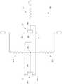
도 1은 다양한 실시예들에 따른 스위치 회로(100)를 도시한다. 스위치 회로(100)는 절연 층 상에 실리콘 층이 배치되는 실리콘 온 절연체(silicon on insulator; SOI)일 수 있으며, 그것은 매립형 산화물(buried oxide; BOX) 층이라고 지칭될 수도 있다. 일부 실시예에서, 추가적인 실리콘 층이 절연 층 아래에 배치될 수 있다.1 illustrates a
다양한 실시예들에서, 최상부 실리콘 층은 대략 50 내지 90 ㎚의 두께를 가질 수 있으며, 실리콘 이산화물 또는 사파이어 층일 수 있는 절연 층은 대략 100 내지 200 ㎚의 두께를 가질 수 있다. 일부 실시예들에서, 스위치 회로(100)는, 도핑된 채널 아래의 실리콘이 이동 전하 캐리어들의 부분적 공핍인 PDSOI 디바이스일 수 있다. 부분적으로 공핍된 영역은 준중성 영역이라고 지칭될 수 있다.In various embodiments, the top silicon layer may have a thickness of approximately 50-90 nm, and the insulating layer, which may be a silicon dioxide or sapphire layer, may have a thickness of approximately 100-200 nm. In some embodiments, the
스위치 회로(100)는 스위치 트랜지스터(104)를 포함할 수 있다. 스위치 회로(100)가 PDSOI인 실시예들에서, 스위치 트랜지스터(104)는 준중성 영역에 전하들을 축적하는 성향을 가질 수 있다. 본 명세서에 개시된 실시예들은, FBE 문제들을 해결하도록 고안된 다른 기술들과 관련된 전술한 문제들의 적어도 일부를 완화시키면서, 이들 축적된 전하들의 방전을 제공한다.The
스위치 트랜지스터(104)는 게이트 컨택트(108), 소스 컨택트(112), 드레인 컨택트(116) 및 바디 컨택트(120)를 포함할 수 있다. 스위치 회로(100)는 서로 직렬로 연결되고, 또한 도시된 바와 같이 소스 컨택트(112)와 드레인 컨택트(116) 사이에서 그들과 연결되는 저항기들(124, 128)을 더 포함할 수 있다. 일부 실시예들에서, 저항기들(124, 128)은 동일한 크기일 수 있다. 스위치 회로(100)는 게이트 컨택트(108)와 연결된 저항기(130)를 더 포함할 수 있다.The
도 1에서 스위치 트랜지스터(104)는 NMOS로서 일반적으로 도시되지만, 다른 실시예들에서, 스위치 트랜지스터(104)는 PMOS일 수 있다.Although
스위치 회로(100)는 방전 트랜지스터(132)를 더 포함할 수 있다. 방전 트랜지스터(132)는 스위치 트랜지스터(104)의 준중성 영역에 축적되는 전하들을 방전시키기 위한 방전 경로를 생성하도록 동작할 수 있다. 방전 트랜지스터(132)는 게이트 컨택트(136), 소스 컨택트(140) 및 드레인 컨택트(144)를 포함할 수 있다. 게이트 컨택트(136)는 저항기들(124, 128) 사이에 위치되는 노드(148)와 연결될 수 있고, 소스 컨택트(140)는 바디 컨택트(120)와 연결될 수 있으며, 드레인 컨택트(144)는 게이트 컨택트(108)와 연결될 수 있다.The
저항기들(124, 128)은 노드(148)에서, 그에 따라 게이트 컨택트(136)에서, 가상 접지(virtual ground), 예를 들면, 고정 전위를 제공할 수 있다. 바디 컨택트(120)에 대한 방전 트랜지스터(132)를 이용하여, 드레인 컨택트(116), 및 노드(148)의 고정 전위에 대한 소스 컨택트(112)는 게이트 컨택트(108)와 바디 컨택트(120) 사이의 전위차의 제거를 용이하게 할 수 있으며, 그에 따라 준중성 영역으로부터 전하들이 방전된다.
도 2는 다양한 실시예들에 따른 스위칭 동작(200)의 흐름도를 도시한다. 일부 실시예들에 따르면, 스위칭 동작(200)은 스위치 회로, 예를 들면, 스위치 회로(100)에 의해 수행될 수 있다.2 illustrates a flowchart of a switching operation 200 in accordance with various embodiments. According to some embodiments, the switching operation 200 may be performed by a switch circuit, for example, the
블록(204)에서, 스위칭 동작(200)은 스위치 회로를 턴온하는 것을 포함할 수 있다. 일부 실시예들에서, 스위치 회로는 소스와 드레인 컨택트들 사이에 신호, 예를 들면, 무선 주파수(RF) 신호를 전달하기 위해, 스위치 트랜지스터, 예를 들면, 스위치 트랜지스터(104)를 턴온함으로써 턴온될 수 있다.At block 204, the switching operation 200 may include turning on the switch circuit. In some embodiments, the switch circuit may be turned on by turning on the switch transistor, eg,
일부 실시예들에서, 스위치 트랜지스터는 스위치 트랜지스터의 게이트 컨택트에 포지티브 DC 전압, 예를 들면, 2.5 V를 인가함으로써 턴온될 수 있다. 방전 트랜지스터의 드레인 컨택트, 예를 들면, 드레인 컨택트(144)는 포지티브 DC 전압을 또한 보게 될 것이다. 방전 트랜지스터의 게이트 컨택트, 예를 들면, 게이트 컨택트(136)는 가상 접지에서 0 전압을 볼 수 있다. 이것은 방전 트랜지스터에서 -2.5 V의 게이트-소스 전압 V_gs를 초래할 수 있다. 이것은 방전 트랜지스터를 턴오프시키고, 사실상, 스위치 회로로부터 방전 트랜지스터를 제거한다.In some embodiments, the switch transistor can be turned on by applying a positive DC voltage, for example 2.5 V, to the gate contact of the switch transistor. The drain contact of the discharge transistor, for
블록(208)에서, 스위칭 동작(200)은 스위치 회로를 턴오프하고, 스위치 트랜지스터의 게이트와 바디 사이에 방전 경로를 제공하는 것을 포함할 수 있다. 일부 실시예들에서, 스위치 회로는 신호, 예를 들면, RF 신호의 전달을 막기 위해 스위치 트랜지스터를 턴오프함으로써 턴오프될 수 있다. 일부 실시예들에서, 스위치 트랜지스터는 스위치 트랜지스터의 게이트 컨택트에 네가티브 DC 전압, 예를 들면, -2.5 V를 인가함으로써 턴오프될 수 있다. 방전 트랜지스터의 드레인 컨택트는 네가티브 DC 전압을 또한 보게 될 것이다. 이것은 방전 트랜지스터에서 2.5 V의 V_gs를 초래할 것이다. 이것은 방전 트랜지스터(132)를 턴온시키고, 그로 인해 스위치 트랜지스터의 게이트 컨택트를 스위치 트랜지스터의 바디 컨택트에 연결함으로써 방전 경로를 생성할 것이다. 이것은, Vth 강하가 없을 것이기 때문에, 전압 헤드룸(voltage headroom)을 제공하지 않고서도 수행될 수 있다.In block 208, the switching operation 200 may include turning off the switch circuit and providing a discharge path between the gate and the body of the switch transistor. In some embodiments, the switch circuit can be turned off by turning off the switch transistor to prevent the transfer of a signal, eg, an RF signal. In some embodiments, the switch transistor can be turned off by applying a negative DC voltage, eg, -2.5 V, to the gate contact of the switch transistor. The drain contact of the discharge transistor will also see a negative DC voltage. This will result in V_gs of 2.5 V in the discharge transistor. This will turn on the
스위칭 동작(200)은 일반적으로, NMOS 트랜지스터를 스위치 트랜지스터("NMOS 스위치" 라고도 지칭됨)로서 이용하는 관점에서 기술되지만, PMOS 트랜지스터를 스위치 회로("PMOS 스위치" 라고도 지칭됨)로서 이용하는 실시예들에 적용가능한 스위칭 동작들이 이용될 수 있다. 다양한 실시예들에서, NMOS 트랜지스터는 스위치 트랜지스터의 바디에 네가티브 DC 전압을 전달하도록 스위치 회로에서 방전 트랜지스터로서 이용될 수 있고, PMOS 트랜지스터는 스위치 트랜지스터의 바디에 포지티브 DC 전압을 전달하도록 스위치 회로에서 이용될 수 있다.Switching operation 200 is generally described in terms of using an NMOS transistor as a switch transistor (also referred to as an "NMOS switch"), but in embodiments that use a PMOS transistor as a switch circuit (also referred to as a "PMOS switch"). Applicable switching operations may be used. In various embodiments, the NMOS transistor can be used as a discharge transistor in a switch circuit to deliver a negative DC voltage to the body of the switch transistor, and the PMOS transistor can be used in the switch circuit to deliver a positive DC voltage to the body of the switch transistor. Can be.
전술한 바와 같이 스위치 회로(100)를 이용하여 방전 경로를 제공하는 것은 다이오드-접속 FET 스위치 회로와 관련되는 전압 임계값 헤드룸과 관련된 동일한 패널티를 초래하지 않는다. 다이오드-접속 FET 스위치 회로에 대하여, 예시적인 시뮬레이션들이 도시되었으며, 스위치 회로(100)는 IMD에 대한 3 dB 개선, 3차 고조파에 대한 2.5 dB 개선 및 2차 고조파에 대한 1.5 dB 개선과 관련될 수 있다.Providing a discharge path using the
전술한 바와 같이 스위치 회로(100)를 이용하여 방전 경로를 제공하는 것은 저항성 바디 컨택트(BC) 스위치 회로와 관련되는 삽입 손실과 관련된 동일한 패널티를 초래하지 않는다. 저항성 BC 스위치 회로에 대하여, 예시적인 시뮬레이션들이 도시되었으며, 스위치 회로(100)는 삽입 손실에 대한 40 mdB(millidecible) 이상의 개선, IMD에 대한 1 dB 개선, 2차 고조파에 대한 3.5 dB 개선 및 3차 고조파에 대한 0.5 dB 개선과 관련될 수 있다.Providing a discharge path using the
스위치 회로(100)는 공통-게이트 증폭기일 수 있으며, 제한적인 것은 아니지만, CMOS(complementary metal oxide semiconductor) 스위치, 전력 증폭기, LNA(low-noise amplifier), 버퍼, 듀플렉서 등을 포함하는 다수의 응용들로 통합될 수 있다.
스위치 회로(100)는 다양한 시스템 내로 통합될 수 있다. 예시적인 시스템(300)의 블록도가 도 3에 도시된다. 도시된 바와 같이, 시스템(300)은, 일부 실시예들에서 무선 주파수(RF) PA 모듈일 수 있는 전력 증폭기(PA) 모듈(302)을 포함한다. 시스템(300)은, 도시된 바와 같이, PA 모듈(302)과 연결된 트랜시버(304)를 포함할 수 있다. PA 모듈(302)은 증폭, 스위칭, 믹싱 등과 같은 임의의 다양한 동작들을 수행하기 위한 스위치 회로(100)를 포함할 수 있다. 다양한 실시예들에서, 스위치 회로(예를 들면, 스위치 회로(100))는 추가적으로/대안적으로, 예를 들면, 상향 변환(up-converting)을 제공하기 위해 트랜시버(304)에 포함되거나, 또는 다양한 스위칭 기능들을 제공하기 위해 안테나 스위치 모듈(antenna switch module; ASM)(306)에 포함될 수 있다.The
PA 모듈(302)은 트랜시버(304)로부터 RF 입력 신호 RFin을 수신할 수 있다. PA 모듈(302)은 RF 입력 신호 RFin을 증폭하여 RF 출력 신호 RFout을 제공할 수 있다. RF 입력 신호 RFin 및 RF 출력 신호 RFout은 둘다, 도 3에서 Tx-RFin 및 Tx-RFout에 의해 각각 표시되는 송신 체인의 일부일 수 있다.The
증폭된 RF 출력 신호 RFout은 ASM(306)에 제공될 수 있으며, ASM(306)은 안테나 구조(308)를 통한 RF 출력 신호 RFout의 OTA(over-the-air) 송신을 실행한다. ASM(306)은 안테나 구조(308)를 통해 RF 신호들을 또한 수신하고, 수신된 RF 신호들 Rx를 수신 체인을 따라 트랜시버(304)에 연결한다.The amplified RF output signal RFout may be provided to the
다양한 실시예들에서, 안테나 구조(308)는, 예를 들면, 다이폴 안테나, 모노폴 안테나, 패치 안테나, 루프 안테나, 마이크로스트립 안테나, 또는 RF 신호들의 OTA 송신/수신에 적합한 임의의 다른 유형의 안테나를 포함하는, 하나 이상의 지향성 및/또는 무지향성 안테나를 포함할 수 있다.In various embodiments,
시스템(300)은 전력 증폭을 포함하는 임의의 시스템일 수 있다. 다양한 실시예들에서, RF 신호를 스위칭하기 위해 시스템(300)에 스위치 회로(100)를 포함하는 것은, 시스템(300)이 높은 RF 전력 및 주파수에서의 전력 증폭을 위해 이용될 때, 특히 유용할 수 있다. 예를 들어, 시스템(300) 내에 스위치 회로(100)를 포함하는 것은, 대략 32 dBm 이상의 전력 및 대략 1800 MHz 이상의 주파수를 갖는 모바일 통신(GSM) 신호들 뿐만 아니라, 대략 34 dBm 이상의 전력을 갖는, 예를 들면, 800 MHz 내지 915 MHz의 보다 낮은 대역의 GSM 신호들을 위한 글로벌 시스템의 송신을 위해 특히 이로울 수 있다.
시스템(300)은 지상파 및 위성 통신들, 레이더 시스템들 중 임의의 하나 이상에 대해, 그리고 가능하게는 다양한 산업 및 의료 응용들에서 적합할 수 있다. 특히, 다양한 실시예들에서, 시스템(300)은 레이더 장치, 위성 통신 장치, 모바일 컴퓨팅 장치(예를 들면, 전화기, 태블릿, 랩탑 등), 기지국, 브로드캐스트 라디오(broadcast radio), 또는 텔레비젼 증폭기 시스템 중 선택된 하나일 수 있다.
본 개시내용은 위에서 예시된 실시예들의 관점에서 기술되었지만, 본 기술 분야의 당업자라면, 동일한 목적을 달성하기 위해 계산된 다양한 대안적 및/또는 등가의 구현들이, 본 개시내용의 영역을 벗어나지 않고서도, 도시되고 기술된 특정 실시예들을 대체할 수 있음을 이해할 것이다. 본 기술 분야의 당업자라면, 본 개시내용의 내용은 매우 다양한 실시예들에서 구현될 수 있음을 쉽게 이해할 것이다. 이러한 설명은 제한적인 것이 아닌, 예시적인 것으로 간주되도록 의도된다.
Although the present disclosure has been described in terms of the embodiments illustrated above, those of ordinary skill in the art will appreciate that various alternative and / or equivalent implementations calculated to achieve the same purpose may be made without departing from the scope of the present disclosure. It will be appreciated that the specific embodiments shown and described may be substituted. Those skilled in the art will readily appreciate that the disclosure may be implemented in a wide variety of embodiments. This description is intended to be considered illustrative and not restrictive.
100 : 스위치 회로
104 : 스위치 트랜지스터
124, 128, 130 : 저항기
132 : 방전 트랜지스터
302 : PA 모듈
304 : 트랜시버100: switch circuit
104: switch transistor
124, 128, 130: resistor
132: discharge transistor
302: PA Module
304: Transceiver
Claims (20)
Translated fromKorean서로 직렬로 연결되고, 상기 소스 컨택트와 상기 드레인 컨택트 사이에서 상기 소스 컨택트 및 드레인 컨택트와 또한 연결되는, 제 1 저항기 및 제 2 저항기와,
상기 스위치 트랜지스터의 상기 바디 컨택트와 연결된 제 1 컨택트, 상기 스위치 트랜지스터의 상기 게이트 컨택트와 연결된 제 2 컨택트, 및 상기 제 1 저항기 및 제 2 저항기와 연결된 게이트 컨택트를 갖는 방전 트랜지스터를 포함하는
회로.
A switch transistor having a gate contact, a source contact, a drain contact, and a body contact;
A first resistor and a second resistor connected in series with each other and also connected with the source contact and the drain contact between the source contact and the drain contact;
A discharge transistor having a first contact coupled with the body contact of the switch transistor, a second contact coupled with the gate contact of the switch transistor, and a gate contact coupled with the first and second resistors;
Circuit.
상기 게이트 컨택트는 상기 제 1 저항기와 제 2 저항기 사이의 제 1 노드와 연결되는
회로.
The method of claim 1,
The gate contact is connected with a first node between the first resistor and the second resistor.
Circuit.
상기 제 1 노드는 가상 접지인
회로.
The method of claim 1,
The first node is virtual ground
Circuit.
상기 회로는 실리콘 온 절연체(silicon on insulator; SOI) 디바이스인
회로.
The method of claim 1,
The circuit is a silicon on insulator (SOI) device
Circuit.
상기 SOI 디바이스는 부분 공핍형 SOI 디바이스를 포함하는
회로.
5. The method of claim 4,
The SOI device includes a partially depleted SOI device.
Circuit.
상기 회로는 네가티브 DC 전압을 전달하도록 구성된 n 채널 금속 산화물 반도체 전계 효과 트랜지스터(NMOS) 스위치인
회로.
The method of claim 1,
The circuit is an n-channel metal oxide semiconductor field effect transistor (NMOS) switch configured to deliver a negative DC voltage.
Circuit.
상기 회로는 포지티브 DC 전압을 전달하도록 구성된 p 채널 금속 산화물 반도체 전계 효과 트랜지스터(PMOS) 스위치인
회로.
The method of claim 1,
The circuit is a p-channel metal oxide semiconductor field effect transistor (PMOS) switch configured to deliver a positive DC voltage.
Circuit.
상기 제 1 저항기와 상기 제 2 저항기는 동일한 크기인
회로.
The method of claim 1,
The first resistor and the second resistor is the same size
Circuit.
상기 방전 트랜지스터의 상기 제 1 컨택트는 상기 방전 트랜지스터의 소스 컨택트이고, 상기 방전 트랜지스터의 상기 제 2 컨택트는 상기 방전 트랜지스터의 드레인 컨택트인
회로.
The method of claim 1,
The first contact of the discharge transistor is a source contact of the discharge transistor, and the second contact of the discharge transistor is a drain contact of the discharge transistor.
Circuit.
상기 회로는 공통-게이트 증폭기를 포함하는
회로.
The method of claim 1,
The circuit includes a common-gate amplifier
Circuit.
턴온될 때 신호를 통과(pass)시키고, 턴오프될 때 상기 신호의 통과를 방지하도록 구성된 제 1 트랜지스터와,
가상 접지를 제공하도록 구성된 노드와,
상기 노드와 연결된 제 1 컨택트 및 상기 제 1 트랜지스터의 바디와 연결되어 상기 제 1 트랜지스터가 턴오프될 때 상기 바디에 방전 경로를 제공하는 제 2 컨택트를 갖는 제 2 트랜지스터를 포함하는
PDSOI 디바이스.
A partially depleted silicon on insulator (PDSOI) device,
A first transistor configured to pass a signal when turned on and to prevent passage of the signal when turned off,
A node configured to provide a virtual ground,
A second transistor having a first contact connected to the node and a second contact connected to a body of the first transistor to provide a discharge path to the body when the first transistor is turned off;
PDSOI device.
상기 제 1 컨택트는 게이트 컨택트이고, 상기 제 2 컨택트는 소스 컨택트인
PDSOI 디바이스.
The method of claim 11,
The first contact is a gate contact and the second contact is a source contact
PDSOI device.
서로 직렬로 연결된 제 1 저항기 및 제 2 저항기를 더 포함하되,
상기 노드는 상기 제 1 저항기와 제 2 저항기 사이에 배치되는
PDSOI 디바이스.
The method of claim 11,
Further comprising a first resistor and a second resistor connected in series with each other,
The node is disposed between the first resistor and the second resistor
PDSOI device.
상기 제 1 트랜지스터는 상기 제 1 저항기와 연결된 소스 컨택트 및 상기 제 2 저항기와 연결된 드레인 컨택트를 포함하는
PDSOI 디바이스.
The method of claim 11,
The first transistor includes a source contact connected with the first resistor and a drain contact connected with the second resistor.
PDSOI device.
상기 제 2 트랜지스터는 상기 제 1 트랜지스터가 턴온될 때 턴오프되도록 구성되는
PDSOI 디바이스.
The method of claim 11,
The second transistor is configured to be turned off when the first transistor is turned on
PDSOI device.
상기 제 2 트랜지스터는 상기 제 1 트랜지스터가 턴오프될 때 턴온되도록 또한 구성되는
PDSOI 디바이스.
The method of claim 15,
The second transistor is further configured to be turned on when the first transistor is turned off
PDSOI device.
상기 트랜시버로부터 상기 신호를 수신하고, 송신을 위해 상기 신호를 증폭하도록 구성된 전력 증폭 모듈(power amplification module)과,
상기 트랜시버 또는 상기 전력 증폭 모듈 내에 배치된 스위치 회로 -상기 스위치 회로는 부분 공핍형 실리콘 온 절연체(PDSOI) 디바이스를 포함함- 를 포함하고,
상기 PDSOI 디바이스는,
상기 신호를 스위칭하도록 구성된 스위치 트랜지스터와,
제 1 노드에서 가상 접지를 제공하도록 구성된 한 쌍의 저항기와,
상기 스위치 트랜지스터 및 상기 제 1 노드와 연결되고, 상기 스위치 트랜지스터의 바디에서의 전하들을 방전시키기 위한 방전 경로를 제공하도록 구성된 방전 트랜지스터를 포함하는
시스템.
A transceiver configured to provide a signal,
A power amplification module configured to receive the signal from the transceiver and amplify the signal for transmission;
A switch circuit disposed within the transceiver or the power amplification module, the switch circuit including a partially depleted silicon on insulator (PDSOI) device,
The PDSOI device,
A switch transistor configured to switch the signal;
A pair of resistors configured to provide virtual ground at the first node,
A discharge transistor coupled with the switch transistor and the first node and configured to provide a discharge path for discharging charges in the body of the switch transistor;
system.
상기 방전 트랜지스터는 상기 스위치 트랜지스터가 턴오프될 때 상기 방전 경로를 제공하도록 구성되는
시스템.
The method of claim 17,
The discharge transistor is configured to provide the discharge path when the switch transistor is turned off
system.
상기 신호는 32 dBM 이상의 전력으로 송신되고, 1800 MHz 이상의 주파수를 갖는
시스템.
The method of claim 17,
The signal is transmitted at power of 32 dBM or higher and has a frequency of 1800 MHz or higher.
system.
상기 신호는 34 dBM 이상의 전력으로 송신되고, 800 MHz 내지 915 MHz 내의 주파수를 갖는
시스템.The method of claim 17,
The signal is transmitted at a power of 34 dBM or more and has a frequency within 800 MHz to 915 MHz.
system.
Applications Claiming Priority (2)
| Application Number | Priority Date | Filing Date | Title |
|---|---|---|---|
| US13/535,203 | 2012-06-27 | ||
| US13/535,203US8829967B2 (en) | 2012-06-27 | 2012-06-27 | Body-contacted partially depleted silicon on insulator transistor |
Publications (1)
| Publication Number | Publication Date |
|---|---|
| KR20140001145Atrue KR20140001145A (en) | 2014-01-06 |
Family
ID=49777498
Family Applications (1)
| Application Number | Title | Priority Date | Filing Date |
|---|---|---|---|
| KR1020130073469AAbandonedKR20140001145A (en) | 2012-06-27 | 2013-06-26 | Body-contacted partially depleted silicon on insulator transistor |
Country Status (4)
| Country | Link |
|---|---|
| US (1) | US8829967B2 (en) |
| KR (1) | KR20140001145A (en) |
| CN (1) | CN103516342B (en) |
| TW (1) | TWI595751B (en) |
Families Citing this family (17)
| Publication number | Priority date | Publication date | Assignee | Title |
|---|---|---|---|---|
| US9628075B2 (en) | 2012-07-07 | 2017-04-18 | Skyworks Solutions, Inc. | Radio-frequency switch having dynamic body coupling |
| US9160328B2 (en) | 2012-07-07 | 2015-10-13 | Skyworks Solutions, Inc. | Circuits, devices, methods and applications related to silicon-on-insulator based radio-frequency switches |
| US10147724B2 (en) | 2012-07-07 | 2018-12-04 | Skyworks Solutions, Inc. | Feed-forward circuit to improve intermodulation distortion performance of radio-frequency switch |
| US9059702B2 (en) | 2012-07-07 | 2015-06-16 | Skyworks Solutions, Inc. | Switch linearization by non-linear compensation of a field-effect transistor |
| US9276570B2 (en) | 2012-07-07 | 2016-03-01 | Skyworks Solutions, Inc. | Radio-frequency switch having gate node voltage compensation network |
| US8975950B2 (en) | 2012-07-07 | 2015-03-10 | Skyworks Solutions, Inc. | Switching device having a discharge circuit for improved intermodulation distortion performance |
| US20140009209A1 (en)* | 2012-07-07 | 2014-01-09 | Skyworks Solutions, Inc. | Radio-frequency switch having dynamic body coupling |
| US9148194B2 (en) | 2012-07-07 | 2015-09-29 | Skyworks Solutions, Inc. | Radio-frequency switch system having improved intermodulation distortion performance |
| US9013225B2 (en) | 2013-02-04 | 2015-04-21 | Skyworks Solutions, Inc. | RF switches having increased voltage swing uniformity |
| US9214932B2 (en) | 2013-02-11 | 2015-12-15 | Triquint Semiconductor, Inc. | Body-biased switching device |
| US8977217B1 (en)* | 2013-02-20 | 2015-03-10 | Triquint Semiconductor, Inc. | Switching device with negative bias circuit |
| US9203396B1 (en) | 2013-02-22 | 2015-12-01 | Triquint Semiconductor, Inc. | Radio frequency switch device with source-follower |
| US9379698B2 (en) | 2014-02-04 | 2016-06-28 | Triquint Semiconductor, Inc. | Field effect transistor switching circuit |
| US9503074B2 (en) | 2015-03-06 | 2016-11-22 | Qualcomm Incorporated | RF circuit with switch transistor with body connection |
| EP3142146A1 (en) | 2015-09-09 | 2017-03-15 | Nokia Technologies Oy | Silicon-on-insultor chip with improved harmonics and linearity, and design method thereof |
| US11916546B2 (en) | 2021-02-25 | 2024-02-27 | Infineon Technologies Ag | RF switch with compensation and gate bootstrapping |
| US20230353140A1 (en)* | 2022-04-29 | 2023-11-02 | Shaoxing Yuanfang Semiconductor Co., Ltd. | Biasing body node of a transistor |
Family Cites Families (81)
| Publication number | Priority date | Publication date | Assignee | Title |
|---|---|---|---|---|
| US3551788A (en) | 1968-09-13 | 1970-12-29 | Servo Corp Of America | High voltage transistorized stack with leakage current compensation |
| US3699359A (en) | 1971-04-20 | 1972-10-17 | Philco Ford Corp | Electronic latching device |
| US4053916A (en) | 1975-09-04 | 1977-10-11 | Westinghouse Electric Corporation | Silicon on sapphire MOS transistor |
| DE2851789C2 (en) | 1978-11-30 | 1981-10-01 | Licentia Patent-Verwaltungs-Gmbh, 6000 Frankfurt | Circuit for switching and transmitting alternating voltages |
| US4491750A (en) | 1982-09-28 | 1985-01-01 | Eaton Corporation | Bidirectionally source stacked FETs with drain-referenced common gating |
| JPH01254014A (en) | 1988-04-04 | 1989-10-11 | Toshiba Corp | power amplifier |
| JPH07105447B2 (en) | 1988-12-15 | 1995-11-13 | 株式会社東芝 | Transmission gate |
| US5313083A (en) | 1988-12-16 | 1994-05-17 | Raytheon Company | R.F. switching circuits |
| US5105164A (en) | 1989-02-28 | 1992-04-14 | At&T Bell Laboratories | High efficiency uhf linear power amplifier |
| US5012123A (en) | 1989-03-29 | 1991-04-30 | Hittite Microwave, Inc. | High-power rf switching system |
| JPH0732335B2 (en) | 1990-11-16 | 1995-04-10 | 日本電信電話株式会社 | High frequency amplifier |
| JP3243892B2 (en) | 1993-05-21 | 2002-01-07 | ソニー株式会社 | Signal switch |
| US5973382A (en) | 1993-07-12 | 1999-10-26 | Peregrine Semiconductor Corporation | Capacitor on ultrathin semiconductor on insulator |
| US5416043A (en) | 1993-07-12 | 1995-05-16 | Peregrine Semiconductor Corporation | Minimum charge FET fabricated on an ultrathin silicon on sapphire wafer |
| US5863823A (en) | 1993-07-12 | 1999-01-26 | Peregrine Semiconductor Corporation | Self-aligned edge control in silicon on insulator |
| US5572040A (en) | 1993-07-12 | 1996-11-05 | Peregrine Semiconductor Corporation | High-frequency wireless communication system on a single ultrathin silicon on sapphire chip |
| US5973363A (en) | 1993-07-12 | 1999-10-26 | Peregrine Semiconductor Corp. | CMOS circuitry with shortened P-channel length on ultrathin silicon on insulator |
| US5930638A (en) | 1993-07-12 | 1999-07-27 | Peregrine Semiconductor Corp. | Method of making a low parasitic resistor on ultrathin silicon on insulator |
| US5452473A (en)* | 1994-02-28 | 1995-09-19 | Qualcomm Incorporated | Reverse link, transmit power correction and limitation in a radiotelephone system |
| US5553295A (en) | 1994-03-23 | 1996-09-03 | Intel Corporation | Method and apparatus for regulating the output voltage of negative charge pumps |
| JP2801563B2 (en) | 1994-08-30 | 1998-09-21 | 松下電器産業株式会社 | Transmission / reception circuit of communication radio, semiconductor integrated circuit device, and communication radio |
| JPH08148949A (en) | 1994-11-18 | 1996-06-07 | Fujitsu Ltd | High frequency amplifier |
| FR2742942B1 (en) | 1995-12-26 | 1998-01-16 | Sgs Thomson Microelectronics | HIGH VOLTAGE SLOT GENERATOR |
| US5777530A (en) | 1996-01-31 | 1998-07-07 | Matsushita Electric Industrial Co., Ltd. | Switch attenuator |
| JP3484462B2 (en) | 1996-04-11 | 2004-01-06 | 株式会社ルネサステクノロジ | Method for estimating lifetime of floating SOI-MOSFET |
| JPH09284114A (en) | 1996-04-19 | 1997-10-31 | Toshiba Microelectron Corp | Analog input circuit |
| GB2331879B (en) | 1996-08-05 | 2001-03-28 | Mitsubishi Electric Corp | Radio-frequency integrated circuit for a radio-frequency wireless transmitter-receiver with reduced influence by radio-frequency power leakage |
| US5818099A (en) | 1996-10-03 | 1998-10-06 | International Business Machines Corporation | MOS high frequency switch circuit using a variable well bias |
| US5920233A (en) | 1996-11-18 | 1999-07-06 | Peregrine Semiconductor Corp. | Phase locked loop including a sampling circuit for reducing spurious side bands |
| JPH10242829A (en) | 1997-02-24 | 1998-09-11 | Sanyo Electric Co Ltd | Switch circuit device |
| JP3441330B2 (en) | 1997-02-28 | 2003-09-02 | 株式会社東芝 | Semiconductor device and manufacturing method thereof |
| US6160292A (en) | 1997-04-23 | 2000-12-12 | International Business Machines Corporation | Circuit and methods to improve the operation of SOI devices |
| US6245161B1 (en) | 1997-05-12 | 2001-06-12 | Silicon Genesis Corporation | Economical silicon-on-silicon hybrid wafer assembly |
| US6033974A (en) | 1997-05-12 | 2000-03-07 | Silicon Genesis Corporation | Method for controlled cleaving process |
| US6180496B1 (en) | 1997-08-29 | 2001-01-30 | Silicon Genesis Corporation | In situ plasma wafer bonding method |
| JPH11136111A (en) | 1997-10-30 | 1999-05-21 | Sony Corp | High frequency circuit |
| JP3711193B2 (en) | 1998-01-16 | 2005-10-26 | 三菱電機株式会社 | Transmission / reception switching circuit |
| US5959488A (en) | 1998-01-24 | 1999-09-28 | Winbond Electronics Corp. | Dual-node capacitor coupled MOSFET for improving ESD performance |
| US6271067B1 (en) | 1998-02-27 | 2001-08-07 | Micron Technology, Inc. | Methods of forming field effect transistors and field effect transistor circuitry |
| US6249027B1 (en) | 1998-06-08 | 2001-06-19 | Sun Microsystems, Inc. | Partially depleted SOI device having a dedicated single body bias means |
| JP2000022160A (en) | 1998-07-06 | 2000-01-21 | Hitachi Ltd | Semiconductor integrated circuit and method of manufacturing the same |
| JP4360702B2 (en) | 1998-08-07 | 2009-11-11 | 株式会社ルネサステクノロジ | Semiconductor device |
| JP3408762B2 (en) | 1998-12-03 | 2003-05-19 | シャープ株式会社 | Semiconductor device having SOI structure and method of manufacturing the same |
| US6171965B1 (en) | 1999-04-21 | 2001-01-09 | Silicon Genesis Corporation | Treatment method of cleaved film for the manufacture of substrates |
| AU6905000A (en) | 1999-08-10 | 2001-03-05 | Silicon Genesis Corporation | A cleaving process to fabricate multilayered substrates using low implantation doses |
| JP3608456B2 (en) | 1999-12-08 | 2005-01-12 | セイコーエプソン株式会社 | Manufacturing method of SOI structure MIS field effect transistor |
| US6504212B1 (en) | 2000-02-03 | 2003-01-07 | International Business Machines Corporation | Method and apparatus for enhanced SOI passgate operations |
| JP3504212B2 (en) | 2000-04-04 | 2004-03-08 | シャープ株式会社 | Semiconductor device with SOI structure |
| JP2002033399A (en) | 2000-07-13 | 2002-01-31 | Toshiba Corp | Semiconductor integrated circuit and its manufacturing method |
| US6816016B2 (en) | 2000-08-10 | 2004-11-09 | Tropian, Inc. | High-efficiency modulating RF amplifier |
| US6496074B1 (en) | 2000-09-28 | 2002-12-17 | Koninklijke Philips Electronics N.V. | Cascode bootstrapped analog power amplifier circuit |
| US6978437B1 (en) | 2000-10-10 | 2005-12-20 | Toppan Photomasks, Inc. | Photomask for eliminating antenna effects in an integrated circuit and integrated circuit manufacture with same |
| JP4434474B2 (en) | 2000-11-29 | 2010-03-17 | Necエレクトロニクス株式会社 | MOS transistor simulation test method |
| TWI230392B (en) | 2001-06-18 | 2005-04-01 | Innovative Silicon Sa | Semiconductor device |
| US6819938B2 (en) | 2001-06-26 | 2004-11-16 | Qualcomm Incorporated | System and method for power control calibration and a wireless communication device |
| KR100906356B1 (en) | 2001-08-10 | 2009-07-06 | 히타치 긴조쿠 가부시키가이샤 | Bypass filter |
| JP3986780B2 (en) | 2001-08-17 | 2007-10-03 | 三菱電機株式会社 | Complementary push-pull amplifier |
| US6804502B2 (en) | 2001-10-10 | 2004-10-12 | Peregrine Semiconductor Corporation | Switch circuit and method of switching radio frequency signals |
| US7796969B2 (en) | 2001-10-10 | 2010-09-14 | Peregrine Semiconductor Corporation | Symmetrically and asymmetrically stacked transistor group RF switch |
| JP3813869B2 (en) | 2001-12-20 | 2006-08-23 | 松下電器産業株式会社 | Field effect transistor switch circuit |
| JP3947044B2 (en) | 2002-05-31 | 2007-07-18 | 富士通株式会社 | Input/Output Buffers |
| US6642578B1 (en) | 2002-07-22 | 2003-11-04 | Anadigics, Inc. | Linearity radio frequency switch with low control voltage |
| JP3445608B2 (en) | 2002-10-25 | 2003-09-08 | 株式会社東芝 | Digital information management system including video information |
| JP2004205301A (en) | 2002-12-25 | 2004-07-22 | Nec Corp | Evaluation device and circuit designing method used therefor |
| JP4257971B2 (en) | 2003-03-27 | 2009-04-30 | 独立行政法人産業技術総合研究所 | Method for applying gate signal of double gate field effect transistor |
| JP4342970B2 (en) | 2004-02-02 | 2009-10-14 | 株式会社東芝 | Semiconductor memory device and manufacturing method thereof |
| US7042044B2 (en) | 2004-02-18 | 2006-05-09 | Koucheng Wu | Nor-type channel-program channel-erase contactless flash memory on SOI |
| US7072217B2 (en) | 2004-02-24 | 2006-07-04 | Micron Technology, Inc. | Multi-state memory cell with asymmetric charge trapping |
| US7158067B2 (en) | 2005-01-31 | 2007-01-02 | The United States Of America As Represented By The Secretary Of The Navy | Analog to digital converter using sawtooth voltage signals with differential comparator |
| US7402850B2 (en) | 2005-06-21 | 2008-07-22 | Micron Technology, Inc. | Back-side trapped non-volatile memory device |
| US7910993B2 (en) | 2005-07-11 | 2011-03-22 | Peregrine Semiconductor Corporation | Method and apparatus for use in improving linearity of MOSFET's using an accumulated charge sink |
| US8742502B2 (en) | 2005-07-11 | 2014-06-03 | Peregrine Semiconductor Corporation | Method and apparatus for use in improving linearity of MOSFETs using an accumulated charge sink-harmonic wrinkle reduction |
| US20080076371A1 (en) | 2005-07-11 | 2008-03-27 | Alexander Dribinsky | Circuit and method for controlling charge injection in radio frequency switches |
| US7890891B2 (en) | 2005-07-11 | 2011-02-15 | Peregrine Semiconductor Corporation | Method and apparatus improving gate oxide reliability by controlling accumulated charge |
| US20070023833A1 (en) | 2005-07-28 | 2007-02-01 | Serguei Okhonin | Method for reading a memory cell having an electrically floating body transistor, and memory cell and array implementing same |
| WO2007018037A1 (en) | 2005-08-09 | 2007-02-15 | Hitachi Metals, Ltd. | High-frequency switch circuit |
| JP4724498B2 (en)* | 2005-08-30 | 2011-07-13 | ルネサスエレクトロニクス株式会社 | Semiconductor integrated circuit device and high frequency power amplification module |
| US7863691B2 (en) | 2008-03-10 | 2011-01-04 | International Business Machines Corporation | Merged field effect transistor cells for switching |
| US8462473B2 (en)* | 2010-12-21 | 2013-06-11 | Microchip Technology Incorporated | Adaptive electrostatic discharge (ESD) protection circuit |
| US9160328B2 (en) | 2012-07-07 | 2015-10-13 | Skyworks Solutions, Inc. | Circuits, devices, methods and applications related to silicon-on-insulator based radio-frequency switches |
| JP5575348B1 (en) | 2014-01-20 | 2014-08-20 | 株式会社Leap | Connector manufacturing method |
- 2012
- 2012-06-27USUS13/535,203patent/US8829967B2/ennot_activeExpired - Fee Related
- 2013
- 2013-06-24TWTW102122337Apatent/TWI595751B/ennot_activeIP Right Cessation
- 2013-06-25CNCN201310254880.0Apatent/CN103516342B/ennot_activeExpired - Fee Related
- 2013-06-26KRKR1020130073469Apatent/KR20140001145A/ennot_activeAbandoned
Also Published As
| Publication number | Publication date |
|---|---|
| CN103516342B (en) | 2018-03-23 |
| CN103516342A (en) | 2014-01-15 |
| TWI595751B (en) | 2017-08-11 |
| TW201409955A (en) | 2014-03-01 |
| US8829967B2 (en) | 2014-09-09 |
| US20140002171A1 (en) | 2014-01-02 |
Similar Documents
| Publication | Publication Date | Title |
|---|---|---|
| US8829967B2 (en) | Body-contacted partially depleted silicon on insulator transistor | |
| US9379698B2 (en) | Field effect transistor switching circuit | |
| US20110221519A1 (en) | Semiconductor integrated circuit and high frequency module using the same | |
| US9559644B2 (en) | Low noise amplifier | |
| US7843280B2 (en) | Systems, methods, and apparatuses for high power complementary metal oxide semiconductor (CMOS) antenna switches using body switching and substrate junction diode controlling in multistacking structure | |
| KR102312044B1 (en) | Bias-boosting bias circuit for radio frequency power amplifier | |
| US9214932B2 (en) | Body-biased switching device | |
| JP6440348B2 (en) | Non-negative bias switching device | |
| US8847672B2 (en) | Switching device with resistive divider | |
| US20090073078A1 (en) | Systems, Methods and Apparatuses for High Power Complementary Metal Oxide Semiconductor (CMOS) Antenna Switches Using Body Switching and External Component in Multi-Stacking Structure | |
| JP6616949B2 (en) | Low noise amplifier drain switch circuit | |
| HK1215895A1 (en) | Ldmos bulk finfet device, method for forming the same and communication device | |
| US8977217B1 (en) | Switching device with negative bias circuit | |
| US10256775B2 (en) | Semiconductor device including an ESD protective element | |
| US20090029654A1 (en) | Using radio frequency transmit/receive switches in radio frequency communications | |
| US9590674B2 (en) | Semiconductor devices with switchable ground-body connection | |
| US20150084702A1 (en) | Electrostatic discharge (esd) circuitry | |
| US9899968B2 (en) | Low noise amplifier circuit | |
| US20160254791A1 (en) | High frequency semiconductor integrated circuit | |
| US9496830B1 (en) | Threshold voltage-tracking bias circuit for radio frequency power amplifier | |
| US9203396B1 (en) | Radio frequency switch device with source-follower | |
| US8385845B1 (en) | Shunt device for switch | |
| JP2012074890A (en) | Switch and control method therefor | |
| US20080106331A1 (en) | Switching Low Noise Amplifier |
Legal Events
| Date | Code | Title | Description |
|---|---|---|---|
| PA0109 | Patent application | Patent event code:PA01091R01D Comment text:Patent Application Patent event date:20130626 | |
| PG1501 | Laying open of application | ||
| PA0201 | Request for examination | Patent event code:PA02012R01D Patent event date:20180622 Comment text:Request for Examination of Application Patent event code:PA02011R01I Patent event date:20130626 Comment text:Patent Application | |
| E902 | Notification of reason for refusal | ||
| PE0902 | Notice of grounds for rejection | Comment text:Notification of reason for refusal Patent event date:20190726 Patent event code:PE09021S01D | |
| E701 | Decision to grant or registration of patent right | ||
| PE0701 | Decision of registration | Patent event code:PE07011S01D Comment text:Decision to Grant Registration Patent event date:20200107 | |
| PC1904 | Unpaid initial registration fee |