KR20130133993A - Member for controlling luminous flux and display device having the same - Google Patents
Member for controlling luminous flux and display device having the sameDownload PDFInfo
- Publication number
- KR20130133993A KR20130133993AKR1020120057176AKR20120057176AKR20130133993AKR 20130133993 AKR20130133993 AKR 20130133993AKR 1020120057176 AKR1020120057176 AKR 1020120057176AKR 20120057176 AKR20120057176 AKR 20120057176AKR 20130133993 AKR20130133993 AKR 20130133993A
- Authority
- KR
- South Korea
- Prior art keywords
- light
- distance
- light emitting
- control member
- flux control
- Prior art date
- Legal status (The legal status is an assumption and is not a legal conclusion. Google has not performed a legal analysis and makes no representation as to the accuracy of the status listed.)
- Granted
Links
Images


Classifications
- G—PHYSICS
- G02—OPTICS
- G02F—OPTICAL DEVICES OR ARRANGEMENTS FOR THE CONTROL OF LIGHT BY MODIFICATION OF THE OPTICAL PROPERTIES OF THE MEDIA OF THE ELEMENTS INVOLVED THEREIN; NON-LINEAR OPTICS; FREQUENCY-CHANGING OF LIGHT; OPTICAL LOGIC ELEMENTS; OPTICAL ANALOGUE/DIGITAL CONVERTERS
- G02F1/00—Devices or arrangements for the control of the intensity, colour, phase, polarisation or direction of light arriving from an independent light source, e.g. switching, gating or modulating; Non-linear optics
- G02F1/01—Devices or arrangements for the control of the intensity, colour, phase, polarisation or direction of light arriving from an independent light source, e.g. switching, gating or modulating; Non-linear optics for the control of the intensity, phase, polarisation or colour
- G02F1/13—Devices or arrangements for the control of the intensity, colour, phase, polarisation or direction of light arriving from an independent light source, e.g. switching, gating or modulating; Non-linear optics for the control of the intensity, phase, polarisation or colour based on liquid crystals, e.g. single liquid crystal display cells
- G02F1/133—Constructional arrangements; Operation of liquid crystal cells; Circuit arrangements
- G02F1/1333—Constructional arrangements; Manufacturing methods
- G02F1/1335—Structural association of cells with optical devices, e.g. polarisers or reflectors
- G02F1/1336—Illuminating devices
- G02F1/133602—Direct backlight
- G02F1/133603—Direct backlight with LEDs
- F—MECHANICAL ENGINEERING; LIGHTING; HEATING; WEAPONS; BLASTING
- F21—LIGHTING
- F21V—FUNCTIONAL FEATURES OR DETAILS OF LIGHTING DEVICES OR SYSTEMS THEREOF; STRUCTURAL COMBINATIONS OF LIGHTING DEVICES WITH OTHER ARTICLES, NOT OTHERWISE PROVIDED FOR
- F21V5/00—Refractors for light sources
- F21V5/008—Combination of two or more successive refractors along an optical axis
- G—PHYSICS
- G02—OPTICS
- G02B—OPTICAL ELEMENTS, SYSTEMS OR APPARATUS
- G02B6/00—Light guides; Structural details of arrangements comprising light guides and other optical elements, e.g. couplings
- G02B6/0001—Light guides; Structural details of arrangements comprising light guides and other optical elements, e.g. couplings specially adapted for lighting devices or systems
Landscapes
- Physics & Mathematics (AREA)
- General Physics & Mathematics (AREA)
- Optics & Photonics (AREA)
- Nonlinear Science (AREA)
- Mathematical Physics (AREA)
- Chemical & Material Sciences (AREA)
- Crystallography & Structural Chemistry (AREA)
- Engineering & Computer Science (AREA)
- General Engineering & Computer Science (AREA)
- Planar Illumination Modules (AREA)
Abstract
Translated fromKoreanDescription
Translated fromKorean실시예는 광속 제어 부재 및 이를 포함하는 표시장치에 관한 것이다.Embodiments relate to a light flux control member and a display device including the same.
통상적으로, 액정표시장치(LCD: liquid crystal display)는 경량, 박형, 저 소비 전력구동 등의 특징으로 인해 그 응용범위가 점차 넓어지고 있는 추세에 있다. 이러한 추세에 따라 액정표시장치는 사무자동화 기기, 오디오/비디오 기기 등에 이용되고 있다. 상기 액정표시장치는 매트릭스 형태로 배열된 다수의 제어용 스위치들에 인가되는 영상신호에 따라 투과량이 조절되어 화면에 원하는 화상을 표시하게 된다.In general, liquid crystal displays (LCDs) have tended to be gradually widened due to their light weight, thinness, and low power consumption. According to this trend, liquid crystal display devices are used in office automation equipment, audio / video equipment, and the like. The liquid crystal display device displays a desired image on the screen by controlling the amount of transmitted light according to a video signal applied to a plurality of control switches arranged in a matrix form.
상기 액정표시장치는 자발광 표시장치가 아니기 때문에 영상이 디스플레이되는 액정표시패널의 배면에 광을 제공하는 백라이트 유닛(backlight unit)이 구비된다.Since the liquid crystal display device is not a self-luminous display device, a backlight unit for providing light to the back of a liquid crystal display panel on which an image is displayed is provided.
일반적인 액정표시장치는 서로 일정간격 이격되어 서로 대향하는 컬러필터 기판 및 어레이 기판과, 상기 컬러필터 기판 및 어레이 기판 사이에 개재된 액정층을 포함하는 액정패널 및 액정패널에 광을 출사하는 백라이트 유닛을 포함한다.A liquid crystal panel including a color filter substrate and an array substrate interposed between the color filter substrate and the array substrate, and a backlight unit for emitting light to the liquid crystal panel .
이와 같은 액정표시장치에 사용되는 백라이트 유닛은 통상적으로 에지형 백라이트 유닛 또는 직하형 백라이트 유닛으로 나누어질 수 있다.The backlight unit used in such a liquid crystal display device can be generally divided into an edge type backlight unit or a direct type backlight unit.
에지형 백라이트 유닛은 도광판 및 발광다이오드들을 포함한다. 발광다이오드들은 도광판의 측면에 배치되고, 도광판은 발광다이오드로부터 출사되는 광을 전반사 등을 통하여 가이드하고, 액정패널을 향하여 출사한다.The edge type backlight unit includes a light guide plate and light emitting diodes. The light emitting diodes are disposed on the side surface of the light guide plate, and the light guide plate guides the light emitted from the light emitting diode through total reflection or the like and emits toward the liquid crystal panel.
직하형 백라이트 유닛은 도광판을 사용하지 않고, 발광다이오드들은 도광판의 후면에 배치된다. 이에 따라서, 발광다이오드들은 액정패널의 후면을 향하여 광을 출사한다.The direct type backlight unit does not use a light guide plate, and the light emitting diodes are disposed on the rear surface of the light guide plate. Accordingly, the light emitting diodes emit light toward the rear surface of the liquid crystal panel.
이와 같은 백라이트 유닛은 액정패널을 향하여 균일하게 광을 출사해야 한다. 즉, 액정표시장치의 휘도 균일성을 향상시키기 위한 노력이 진행 중이다.Such a backlight unit must emit light uniformly toward the liquid crystal panel. That is, efforts are being made to improve the luminance uniformity of the liquid crystal display device.
실시예는 향상된 휘도 균일도를 가지고, 용이하게 제조될 수 있는 광속 제어 부재 및 표시장치를 제공하고자 한다.The embodiment aims to provide a light flux control member and a display device which have improved luminance uniformity and can be easily manufactured.
일 실시예에 따른 광속 제어 부재는 광이 입사되는 입사면; 상기 입사면으로부터의 광이 출사되는 굴절면; 및 상기 입사면으로부터 상기 굴절면으로 연장되는 후면을 포함하고, 상기 입사면의 중심으로부터 상기 굴절면의 중심으로 연장되는 중심축이 정의되고, 상기 중심축에 대하여 수직한 제 1 방향이 정의되고, 상기 중심축에 대하여 수직하고, 상기 제 1 방향과 교차하는 제 2 방향이 정의되고, 상기 제 1 방향을 기준으로, 상기 중심축으로부터 상기 굴절면 및 상기 후면이 만나는 부분까지의 제 1 거리는 상기 제 2 방향을 기준으로, 상기 중심축으로부터 상기 굴절면 및 상기 후면이 만나는 부분까지의 제 2 거리보다 더 작다.The light flux control member according to an exemplary embodiment includes an incident surface on which light is incident; A refracting surface on which light from the incident surface is emitted; And a rear surface extending from the incident surface to the refracting surface, wherein a central axis extending from a center of the incident surface to the center of the refracting surface is defined, a first direction perpendicular to the central axis is defined, Wherein a first distance from the central axis to a portion where the refracting surface and the rear surface meet is defined as a direction perpendicular to the axis and a second direction intersecting the first direction, Is smaller than the second distance from the central axis to the portion where the refracting surface and the rear surface meet.
일 실시예에 따른 표시장치는 제 2 방향으로 연장되는 구동 기판; 상기 구동 기판 상에 배치되는 광원; 상기 구동 기판 상에 배치되고, 상기 광원을 덮는 광속 제어 부재; 및 상기 광속 제어 부재로부터의 광이 입사되는 표시패널을 포함하고, 상기 광속 제어 부재는 상기 광원으로부터의 광이 출사되는 굴절면을 포함하고, 상기 제 2 방향과 교차하고, 상기 광원의 광축에 대하여 수직하는 제 1 방향이 정의되고, 상기 제 2 방향을 기준으로, 상기 광원의 광축으로부터 상기 굴절면까지의 제 2 거리는 상기 제 1 방향을 기준으로, 상기 광원의 광축으로부터 상기 굴절면의 외곽까지의 제 1 거리보다 더 크다.A display device according to an embodiment includes a driving substrate extending in a second direction; A light source disposed on the driving substrate; A light flux control member disposed on the driving substrate and covering the light source; And a display panel on which light from the light flux control member is incident, wherein the light flux control member includes a refracting surface on which light from the light source is emitted, intersects with the second direction, and is perpendicular to the optical axis of the light source And a second distance from the optical axis of the light source to the refracting surface is defined as a first distance from the optical axis of the light source to the outer circumference of the refracting surface with respect to the first direction, .
실시예에 따른 표시장치는 상기 광속 제어 부재들을 제 2 방향으로 연장시킨다. 이에 따라서, 상기 광원들로부터 출사되는 광은 상기 제 2 방향보다 상기 제 2 방향에 대하여 수직한 제 1 방향으로 더 확산된다. 이때, 상기 광원들은 상기 제 2 방향과 실질적으로 평행한 방향으로 열을 지어 배치된다. 또한, 상기 광원들은 상기 제 2 방향으로 조밀하게 배치되고, 상기 제 1 방향으로 덜 조밀하게 배치된다.The display device according to the embodiment extends the light flux control members in the second direction. Accordingly, the light emitted from the light sources is further diffused in the first direction perpendicular to the second direction than the second direction. At this time, the light sources are arranged in rows in a direction substantially parallel to the second direction. Also, the light sources are arranged densely in the second direction, and are arranged less densely in the first direction.
이에 따라서, 상기 광속 제어 부재를 통과한 광은 전체적으로 균일한 휘도로 상기 표시패널에 입사된다.Accordingly, the light having passed through the light flux controlling member is incident on the display panel as a whole with a uniform luminance.
즉, 실시예에 따른 표시장치는 상기 광원들이 배치되는 열들의 수가 감소되더라도, 상기 광속 제어 부재에 의해서, 전체적으로는 높은 휘도 균일도를 가질 수 있다. 즉, 상기 광원들의 열 사이의 간격이 커지더라도, 상기 광속 제어 부재들에 의해서, 상기 제 2 방향으로의 휘도 균일도가 향상될 수 있다.That is, even if the number of rows in which the light sources are arranged is reduced by the light flux control member, the display apparatus according to the embodiment can have a high luminance uniformity as a whole. That is, even if the interval between the rows of the light sources is increased, the brightness uniformity in the second direction can be improved by the light flux control members.
따라서, 실시예에 따른 표시장치는 상기 광원들의 열들의 수를 줄일 수 있고, 사용되는 회로기판들의 수를 줄일 수 있다. 따라서, 실시예에 따른 표시장치는 적은 비용으로 용이하게 제조될 수 있다.Therefore, the display device according to the embodiment can reduce the number of rows of the light sources and reduce the number of circuit boards to be used. Therefore, the display device according to the embodiment can be easily manufactured at a low cost.
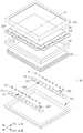
도 1은 실시예에 따른 발광 장치를 도시한 분해 사시도이다.
도 2는 실시예에 따른 발광 장치의 제 1 방향을 기준으로 단면을 도시한 단면도이다.
도 3은 실시예에 따른 발광 장치의 제 2 방향을 기준으로 단면을 도시한 단면도이다.
도 4는 다른 실시예에 따른 광속 제어 부재의 배면을 도시한 사시도이다.
도 5는 다른 실시예에 따른 발광 장치의 제 1 방향을 기준으로 단면을 도시한 단면도이다.
도 6은 다른 실시예에 따른 발광 장치의 제 2 방향을 기준으로 단면을 도시한 단면도이다.
도 7은 제 1 방향을 기준으로, 광속 제어 부재로부터 출사되는 광의 지향각을 도시한 도면이다.
도 8은 제 2 방향을 기준으로, 광속 제어 부재로부터 출사되는 광의 지향각을 도시한 도면이다.
도 9는 실시예에 따른 액정표시장치를 도시한 분해 사시도이다.
도 10은 도 9에서 A-A`를 따라서 절단한 단면을 도시한 단면도이다.
도 11은 제 1 방향을 기준으로 광속 제어 부재로부터 출사되는 광의 경로를 도시한 도면이다.
도 12는 제 2 방향을 기준으로 광속 제어 부재로부터 출사되는 광의 경로를 도시한 도면이다.1 is an exploded perspective view showing a light emitting device according to an embodiment.
2 is a cross-sectional view illustrating a light emitting device according to an embodiment in a first direction.
3 is a cross-sectional view illustrating a light emitting device according to an embodiment in a second direction.
4 is a perspective view showing a back surface of a light flux control member according to another embodiment.
5 is a cross-sectional view illustrating a light emitting device according to another embodiment with reference to a first direction.
6 is a cross-sectional view showing a second embodiment of the light emitting device according to another embodiment.
Fig. 7 is a view showing the directivity angle of light emitted from the light flux control member with reference to the first direction. Fig.
Fig. 8 is a view showing the directivity angle of light emitted from the light flux control member with reference to the second direction. Fig.
9 is an exploded perspective view showing a liquid crystal display device according to an embodiment.
FIG. 10 is a cross-sectional view showing a section cut along AA 'in FIG. 9; FIG.
11 is a diagram showing the path of light emitted from the light flux control member with reference to the first direction.
12 is a diagram showing the path of light emitted from the light flux control member with reference to the second direction.
실시 예의 설명에 있어서, 각 패널, 시트, 부재, 가이드 또는 유닛 등이 각 패널, 시트, 부재, 가이드 또는 유닛 등의 "상(on)"에 또는 "아래(under)"에 형성되는 것으로 기재되는 경우에 있어, "상(on)"과 "아래(under)"는 "직접(directly)" 또는 "다른 구성요소를 개재하여 (indirectly)" 형성되는 것을 모두 포함한다. 또한 각 구성요소의 상 또는 아래에 대한 기준은 도면을 기준으로 설명한다. 도면에서의 각 구성요소들의 크기는 설명을 위하여 과장될 수 있으며, 실제로 적용되는 크기를 의미하는 것은 아니다.In the description of the embodiments, it is described that each panel, sheet, member, guide, unit or the like is formed "on" or "under" of each panel, sheet, member, In this case, "on" and "under " all include being formed either directly or indirectly through another element. In addition, the upper or lower reference of each component is described with reference to the drawings. The size of each component in the drawings may be exaggerated for the sake of explanation and does not mean the size actually applied.
도 1은 실시예에 따른 발광 장치를 도시한 분해 사시도이다. 도 2는 실시예에 따른 발광 장치의 제 1 방향을 기준으로 단면을 도시한 단면도이다. 도 3은 실시예에 따른 발광 장치의 제 2 방향을 기준으로 단면을 도시한 단면도이다. 도 4는 다른 실시예에 따른 광속 제어 부재의 배면을 도시한 사시도이다. 도 5는 다른 실시예에 따른 발광 장치의 제 1 방향을 기준으로 단면을 도시한 단면도이다. 도 6은 다른 실시예에 따른 발광 장치의 제 2 방향을 기준으로 단면을 도시한 단면도이다. 도 7은 제 1 방향을 기준으로, 광속 제어 부재로부터 출사되는 광의 지향각을 도시한 도면이다. 도 8은 제 2 방향을 기준으로, 광속 제어 부재로부터 출사되는 광의 지향각을 도시한 도면이다.1 is an exploded perspective view showing a light emitting device according to an embodiment. 2 is a cross-sectional view illustrating a light emitting device according to an embodiment in a first direction. 3 is a cross-sectional view illustrating a light emitting device according to an embodiment in a second direction. 4 is a perspective view showing a back surface of a light flux control member according to another embodiment. 5 is a cross-sectional view illustrating a light emitting device according to another embodiment with reference to a first direction. 6 is a cross-sectional view showing a second embodiment of the light emitting device according to another embodiment. Fig. 7 is a view showing the directivity angle of light emitted from the light flux control member with reference to the first direction. Fig. Fig. 8 is a view showing the directivity angle of light emitted from the light flux control member with reference to the second direction. Fig.
도 1 내지 도 8을 참조하면, 실시예에 따른 발광 장치는 광속 제어 부재(10), 광원, 예를 들어, 발광다이오드(20) 및 구동 기판(30)을 포함한다.1 to 8, a light emitting device according to an embodiment includes a light
상기 광속 제어 부재(10)는 상기 구동 기판(30) 상에 배치된다. 상기 광속 제어 부재(10)는 상기 발광다이오드(20)를 덮는다. 상기 광속 제어 부재(10)는 상기 발광다이오드(20)의 일부 또는 전부를 수용할 수 있다.The light
상기 광속 제어 부재(10)에는 상기 발광다이오드(20)로부터 출사되는 광이 입사된다. 상기 광속 제어 부재(10)는 상기 발광다이오드(20)에 직접 배치되고, 상기 발광다이오드(20)로부터의 광은 상기 광속 제어 부재(10)에 직접 입사될 수 있다.Light emitted from the
상기 광속 제어 부재(10)는 입사면(210), 굴절면(110, 120) 및 후면(220)을 포함한다.The light
상기 입사면(210)은 상기 발광다이오드(20)로부터 광이 입사되는 면이다. 상기 입사면(210)은 상기 발광다이오드(20)에 대향하는 면이다. 상기 입사면(210)은 상기 발광다이오드(20)와 직접 접촉될 수 있다. 더 자세하게, 상기 입사면(210)은 상기 발광다이오드(20)에 직접 밀착되는 면일 수 있다. 특히, 상기 광속 제어 부재(10)에는 오목부(200)가 형성될 수 있다.The
상기 오목부(200)는 상기 발광다이오드(20)에 대응한다. 또한, 상기 오목부(200)는 상기 함몰부(100)에 대향한다. 상기 오목부(200)는 상기 광속 제어 부재(10)의 하부에 형성된다. 즉, 상기 오목부(200)는 상기 광속 제어 부재(10)의 하부에 형성된다.The
상기 오목부(200)에 상기 발광다이오드(20)가 배치된다. 더 자세하게, 상기 발광다이오드(20)의 일부 또는 전부는 상기 오목부(200) 내에 배치된다. 즉, 상기 발광다이오드(20)의 일부 또는 전부는 상기 광속 제어 부재(10) 내에 배치된다.The
이때, 상기 발광다이오드(20)로부터 출사되는 광은 상기 오목부(200)의 내부면(210)을 통하여 입사될 수 있다. 이에 따라서, 상기 오목부(200)의 내부면(210)은 광이 입사되는 입사면(210)일 수 있다. 즉, 상기 광속 제어 부재(10)에는 상기 오목부(200)의 내부면(210)을 통하여 거의 대부분의 광이 입사될 수 있다.At this time, the light emitted from the
이와는 다르게, 상기 광속 제어 부재(10)에는 상기 오목부(200)가 형성되지 않을 수 있다. 이때, 상기 발광다이오드(20)는 상기 광속 제어 부재(10)의 평평한 후면에 배치될 수 있다. 이때, 상기 후면이 일부가 입사면일 수 있다.Alternatively, the light
또한, 상기 광속 제어 부재(10)에는 함몰부(100)가 형성된다. 상기 함몰부(100)는 상기 광속 제어 부재(10)의 상부에 형성된다. 상기 함몰부(100)는 상기 발광다이오드(20)에 대응된다. 또한, 상기 함몰부(100)는 상기 발광다이오드(20)를 향하여 함몰된다. 더 자세하게, 상기 함몰부(100)는 상기 발광다이오드(20)을 향하여 함몰된다. 상기 함몰부(100)는 상기 광속 제어 부재(10)의 중앙 부분에 형성된다.The light
상기 함몰부(100)의 내부면의 중심(140)은 상기 발광다이오드(20)의 광축(OA)에 배치된다. 즉, 상기 발광다이오드(20)의 광축(OA)은 상기 함몰부(100)의 내부면의 중심(140)을 통과한다.The
또한, 상기 오목부(200)의 내부면(210)의 중심은 상기 발광다이오드(20)의 광축(OA) 상에 배치될 수 있다. 상기 발광다이오드(20)의 광축(OA)은 상기 함몰부(100)의 내부면(110)의 중심(140) 및 상기 오목부(200)의 내부면(210)의 중심을 통과할 수 있다.The center of the
상기 굴절면(110, 120)은 상기 입사면(210)으로부터의 광을 출사시킨다. 또한, 상기 굴절면(110, 120)은 상기 광속 제어 부재(10)에 입사되는 광을 굴절시킨다. 상기 굴절면(110, 120)은 전체적으로 곡면으로 형성될 수 있다. 상기 굴절면(110, 120)은 제 1 굴절면(110) 및 리세스면(120)을 포함한다.The refracting
상기 제 1 굴절면(110)은 상기 후면(220)으로 연장된다. 상기 제 1 굴절면(110)은 상기 후면(220)으로부터 절곡되어, 상방으로 연장될 수 있다. 또한, 상기 제 1 굴절면(110)은 상기 구동 기판(30)의 상면으로부터 상방으로 연장될 수 있다.The first refracting
즉, 상기 제 1 굴절면(110)은 상기 후면(220)으로부터 상기 제 2 굴절면(110, 120)(120)으로 연장된다. 상기 후면(220)은 상기 구동 기판(30)에 대향한다. 상기 후면(220)은 상기 오목부(200)의 내부면(210)으로부터 상기 발광다이오드(20)의 광축(OA)로부터 멀어지는 방향으로 연장된다.That is, the first refracting
상기 제 1 굴절면(110)은 곡면일 수 있다. 더 자세하게, 상기 제 1 굴절면(110)은 구면 또는 비구면일 수 있다. 상기 제 1 굴절면(110)은 상기 발광다이오드(20)로부터의 광을 출사할 수 있다. 또한, 상기 제 1 굴절면(110)은 상기 리세스면(120)에 의해서 반사되는 광을 굴절시킬 수 있다.The first refracting
상기 제 1 굴절면(110)은 상기 후면(220)으로부터 상방으로 연장된다. 또한, 상기 발광다이오드(20)의 광축(OA)로부터 상기 제 1 굴절면(110)까지의 거리는 상기 후면(220)으로부터 멀어질수록 점점 가까워질 수 있다. 상기 발광다이오드(20)의 광축(OA)로부터 상기 제 1 굴절면(110)까지의 거리는 상기 구동 기판(30)으로부터 멀어질수록 점점 작아질 수 있다.The first refracting
상기 리세스면(120)은 상기 함몰부(100)의 내부면이다. 상기 리세스면(120)은 상기 리세스면(120)은 상기 발광다이오드(20)로부터의 광의 일부를 측방, 측상방 또는 측하방으로 반사시킬 수 있다.The recessed
이에 따라서, 상기 리세스면(120)은 상기 광속 제어 부재(10)의 중앙 부분에 과도하게 광이 집중되어 형성되는 핫 스팟(hot spot)이 발생되는 것을 방지할 수 있다. 또한, 상기 리세스면(120)은 상기 발광다이오드(20)로부터의 광을 상기 제 1 굴절면(110)으로 반사시킬 수 있다.Accordingly, the recessed
또한, 상기 리세스면(120)은 상기 발광다이오드(20)로부터의 광의 다른 일부를 굴절시킬 수 있다. 즉, 상기 리세스면(120)은 상기 입사면을 통하여 입사되는 광을 굴절시키는 제 2 굴절면일 수 있다.In addition, the recessed
상기 리세스면(120)은 상기 발광다이오드(20)의 광축(OA)으로부터 연장된다. 더 자세하게, 상기 리세스면(120)은 상기 발광다이오드(20)의 광축(OA)으로부터 멀어지는 방향으로 연장된다. 이때, 상기 발광다이오드(20)의 광축(OA)으로부터 멀어지는 방향은 상기 발광다이오드(20)의 광축(OA)과 직교하거나 경사지는 외곽 방향을 의미할 수 있다. 더 자세하게, 상기 리세스면(120)은 상기 발광다이오드(20)의 광축(OA)으로부터 측상방으로 연장된다. 상기 리세스면(120)은 상기 발광다이오드(20)의 광축(OA)으로부터 외곽으로 연장된다. 여기에서 "광축(OA)"이란, 점광원으로부터 입체적인 출사 광속(luminous flux)의 중심에서의 광의 진행 방향을 말한다.The recessed
또한, 상기 발광다이오드(20)의 광축(OA)은 상기 입사면(210)의 중심 및 상기 굴절면(110, 120)의 중심(140)을 통과할 수 있다. 즉, 상기 발광다이오드(20)의 광축(OA)은 상기 광속 제어 부재(10)의 중심축과 실질적으로 일치할 수 있다. 여기서, 상기 중심축은 상기 입사면(210)의 중심 및 상기 굴절면(110, 120)의 중심(140)을 통과하는 직선일 수 있다.The optical axis OA of the
상기 리세스면(120) 및 상기 발광다이오드(20)의 광축(OA) 사이의 거리는 상기 발광다이오드(20)로부터 멀어질수록 점점 커질 수 있다. 더 자세하게, 상기 리세스면(120) 및 상기 발광다이오드(20)의 광축(OA) 사이의 거리는 상기 발광다이오드(20)로부터 멀어짐에 따라서, 비례적으로 커질 수 있다.The distance between the recessed
상기 리세스면(120) 및 상기 제 1 굴절면(110)은 서로 만날 수 있다. 상기 제 1 굴절면(110)은 상기 리세스면(120)으로부터 만곡되어, 하방으로 연장될 수 있다. 즉, 상기 제 1 굴절면(110)은 상기 리세스면(120)으로부터 만곡되어 상기 후면(220)으로 연장될 수 있다.The recessed
여기서, 만곡은 완만하게 구부러지는 형상을 의미한다. 예를 들어, 두 개의 면들이 약 0.1㎜ 보다 큰 곡률 반지름의 곡면을 형성하며 구부러지는 경우, 두 개의 면들이 만곡된다고 할 수 있다. 여기서, 변곡은 곡면의 변화되는 경향이 바뀌어서 구부러지는 것을 의미한다. 예를 들어, 볼록한 곡면이 구부러지면서 오목한 곡면으로 변화될 때, 볼록한 곡면 및 오목한 곡면이 변곡된다고 할 수 있다.Here, the curve means a shape that is gently bent. For example, if two faces are curved while forming a curved surface with a radius of curvature larger than about 0.1 mm, the two faces may be curved. Here, the curvature means that the curvature of curvature changes and the curvature changes. For example, when the convex curved surface is bent and changed into a concave curved surface, it can be said that the convex curved surface and the concave curved surface are curved.
상기 후면(220)은 상기 입사면(210)으로부터 연장된다. 상기 후면(220)은 상기 구동 기판(30)의 상면과 대향된다. 상기 후면(220)은 상기 구동 기판(30)의 상면과 직접 접촉될 수 있다. 상기 후면(220)은 상기 구동 기판(30)의 상면과 직접 대향될 수 있다.The
상기 후면(220)은 평면일 수 있다. 또한, 상기 후면(220)은 상기 입사면(210)의 주위를 둘러쌀 수 있다. 즉, 상기 후면(220)은 상기 발광다이오드(20)의 주위를 따라서 연장될 수 있다.The
상기 광속 제어 부재(10)는 투명하다. 상기 광속 제어 부재(10)의 굴절율은 약 1.4 내지 약 1.5일 수 있다. 상기 광속 제어 부재(10)는 투명한 수지로 형성될 수 있다. 더 자세하게, 상기 광속 제어 부재(10)는 열 가소성 수지를 포함할 수 있다. 더 자세하게, 상기 광속 제어 부재(10)는 실리콘계 수지를 포함할 수 있다. 상기 광속 제어 부재(10)로 사용되는 물질의 예로서는 폴리디메틸실록산(poly(dimethylsiloxane);PDMS) 등을 들 수 있다.The light
상기 광속 제어 부재(10)는 이방성 구조를 가질 수 있다. 상기 광속 제어 부재(10)는 선대칭이 아닌, 면대칭 구조를 가질 수 있다. 상기 광속 제어 부재(10)는 제 2 방향으로 연장된 형상을 가질 수 있다. 즉, 상기 광속 제어 부재(10)는 상기 제 2 방향으로 상대적으로 길게, 상기 제 2 방향에 대하여 교차하는 제 1 방향으로 상대적으로 짧게 형성될 수 있다. 예를 들어, 탑측에서 보았을 때, 상기 광속 제어 부재(10)는 타원 구조를 가질 수 있다. 또한, 상기 함몰부(100)도 탑측에서 보았을 때, 타원 형상을 가질 수 있다.The light
상기 제 1 방향 및 상기 제 2 방향은 서로 수직으로 교차할 수 있다. 또한, 상기 제 1 방향 및 상기 발광다이오드(20)의 광축(OA)은 서로 수직할 수 있다. 또한, 상기 제 2 방향 및 상기 발광다이오드(20)의 광축(OA)은 서로 수직할 수 있다.The first direction and the second direction may intersect perpendicularly to each other. In addition, the first direction and the optical axis OA of the
도 2에 도시된 바와 같이, 상기 제 1 방향을 기준으로, 상기 발광다이오드(20)의 광축(OA)으로부터 상기 후면(220) 및 상기 제 1 굴절면(110)이 만나는 부분까지의 제 1 거리(D1)가 정의된다. 또한, 도 3에 도시된 바와 같이, 상기 제 2 방향을 기준으로, 상기 발광다이오드(20)의 광축(OA)으로부터 상기 후면(220) 및 상기 제 1 굴절면(110)이 만나는 부분까지의 제 2 거리(D2)가 정의된다. 이때, 상기 제 1 거리(D1)는 상기 제 2 거리(D2)보다 더 작다. 상기 제 1 거리(D1) 및 상기 제 2 거리(D2)의 비는 약 1:1.5 내지 약 1:5일 수 있다. 결국, 상기 제 1 방향을 기준으로, 상기 발광다이오드(20)로부터 상기 후면(220)의 외곽까지의 거리는 상기 제 2 방향을 기준으로, 상기 발광다이오드(20)로부터 상기 후면(220)의 외곽까지의 거리보다 더 작을 수 있다.2, a first distance from the optical axis OA of the
또한, 상기 발광다이오드(20)의 광축(OA)으로부터 상기 후면(220) 및 상기 제 1 굴절면(110)이 만나는 부분까지의 거리는 상기 제 1 방향으로부터 상기 제 2 방향으로 갈수록 점점 더 커질 수 있다.The distance from the optical axis OA of the
도 2에 도시된 바와 같이, 상기 제 1 방향을 기준으로, 상기 발광다이오드(20)의 광축(OA)으로부터 상기 리세스면(120) 및 상기 제 1 굴절면(110)이 만나는 부분까지의 제 3 거리(D3)가 정의된다. 또한, 도 3에 도시된 바와 같이, 상기 제 2 방향을 기준으로, 상기 발광다이오드(20)의 광축(OA)으로부터 상기 리세스면(120) 및 상기 제 1 굴절면(110)이 만나는 부분까지의 제 4 거리(D4)가 정의된다. 이때, 상기 제 3 거리(D3)는 상기 제 4 거리(D4)보다 더 작을 수 있다. 상기 제 3 거리(D3) 및 상기 제 4 거리(D4)의 비는 약 1:1.5 내지 약 1:5일 수 있다.2, from the optical axis OA of the
또한, 상기 발광다이오드(20)의 광축(OA)으로부터 상기 리세스면(120) 및 상기 제 1 굴절면(110)이 만나는 부분까지의 거리는 상기 제 1 방향으로부터 상기 제 2 방향으로 갈수록 점점 더 커질 수 있다.The distance from the optical axis OA of the
또한, 상기 발광다이오드(20)의 광축(OA)을 통과하고, 상기 제 1 방향으로 연장되는 제 1 대칭면이 정의될 수 있다. 즉, 상기 발광다이오드(20)의 광축(OA)은 상기 제 1 대칭면에 배치될 수 있다. 이때, 상기 광속 제어 부재(10)는 상기 제 1 대칭면에 대하여 면대칭 구조를 가질 수 있다. 또한, 상기 입사면, 상기 후면(220) 및 상기 굴절면(110, 120)은 상기 제 1 대칭면에 대하여, 면대칭 구조를 가질 수 있다. 즉, 상기 광속 제어 부재(10)는 상기 제 1 대칭면에 의해서, 서로 동일한 크기로 양분될 수 있다.A first symmetry plane passing through the optical axis OA of the
또한, 상기 발광다이오드(20)의 광축(OA)을 통과하고, 상기 제 2 방향으로 연장되는 제 2 대칭면이 정의될 수 있다. 즉, 상기 발광다이오드(20)의 광축(OA)은 상기 제 2 대칭면에 배치될 수 있다. 이때, 상기 광속 제어 부재(10)는 상기 제 2 대칭면에 대하여 면대칭 구조를 가질 수 있다. 또한, 상기 입사면, 상기 후면(220) 및 상기 굴절면(110, 120)은 상기 제 2 대칭면에 대하여, 면대칭 구조를 가질 수 있다. 즉, 상기 광속 제어 부재(10)는 상기 제 2 대칭면에 의해서, 서로 동일한 크기로 양분될 수 있다.A second symmetry plane passing through the optical axis OA of the
또한, 상기 제 1 대칭면 및 상기 제 2 대칭면에 의해서, 상기 광속 제어 부재(10)는 모두 실질적으로 동일한 크기로, 4등분 될 수 있다. 이에 따라서, 상기 입사면, 상기 후면(220) 및 상기 굴절면(110, 120)은 각각 상기 제 1 대칭면 및 상기 제 2 대칭면에 의해서, 모두 실질적으로 동일한 크기로, 4등분 될 수 있다.Further, by the first symmetry plane and the second symmetry plane, the light
상기 광속 제어 부재(10)는 상기 구동 기판(30)에 직접 형성될 수 있다. 또한, 상기 광속 제어 부재(10)는 상기 발광다이오드(20)에 직접 형성될 수 있다. 상기 광속 제어 부재(10)는 상기 구동 기판(30) 및 상기 발광다이오드(20)에 직접 접촉될 수 있다. 더 자세하게, 상기 광속 제어 부재(10)는 상기 구동 기판(30) 및 상기 발광다이오드(20)에 직접 밀착될 수 있다.The light
이와는 다르게, 상기 광속 제어 부재(10)는 따로 형성되고, 상기 발광다이오드(20)를 덮도록, 상기 구동 기판(30) 상에 배치될 수 있다. 즉, 상기 광속 제어 부재(10)는 접착부에 의해서, 상기 구동 기판(30)에 접착될 수 있다.Alternatively, the light
도 4 내지 도 6에 도시된 바와 같이, 상기 광속 제어 부재(10)는 상기 발광다이오드(20)에 밀착되지 않을 수 있다. 즉, 상기 광속 제어 부재(10)의 오목부(200)의 내부면(210)은 상기 발광다이오드(20)와 이격될 수 있다. 즉, 상기 발광다이오드(20) 및 상기 오목부(200)의 내부면(210) 사이에 공기층 등이 형성될 수 있다.4 to 6, the light
또한, 상기 오목부(200)의 내부면(210)은 전체적으로 곡면으로 형성될 수 있다. 이때, 상기 오목부(200)의 내부면(210)은 상기 발광다이오드(20)로부터의 광이 입사되는 입사면이다. 즉, 상기 입사면은 전체적으로 곡면일 수 있다.In addition, the
상기 오목부(200)는 상기 제 2 방향으로 연장되는 형상을 가질 수 있다. 예를 들어, 상기 오목부(200)는 상기 제 2 방향으로 연장되는 타원 형상을 가질 수 있다.The
또한, 도 5에 도시된 바와 같이, 상기 제 1 방향을 기준으로, 상기 발광다이오드(20)의 광축(OA)으로부터 상기 입사면 및 상기 후면(220)이 만나는 부분까지의 제 5 거리(D5)가 정의될 수 있다. 또한, 도 6에 도시된 바와 같이, 상기 제 2 방향을 기준으로, 상기 발광다이오드(20)의 광축(OA)으로부터 상기 입사면 및 상기 후면(220)이 만나는 부분까지의 제 6 거리(D6)가 정의될 수 있다.5, a fifth distance D5 from the optical axis OA of the
이때, 상기 제 5 거리(D5)는 상기 제 6 거리(D6)보다 더 작을 수 있다. 상기 제 5 거리(D5) 및 상기 제 6 거리(D6)의 비는 약 1:1.1 내지 약 1:10일 수 있다. 또한, 상기 발광다이오드(20)의 광축(OA)으로부터 상기 입사면 및 상기 후면(220)이 만나는 부분까지의 거리는 상기 제 1 방향으로부터 상기 제 2 방향으로 갈수록 점점 더 커질 수 있다.At this time, the fifth distance D5 may be smaller than the sixth distance D6. The ratio of the fifth distance D5 and the sixth distance D6 may be about 1: 1.1 to about 1:10. In addition, the distance from the optical axis OA of the
상기 발광다이오드(20)는 광을 발생시킨다. 상기 발광다이오드(20)는 점광원일 수 있다. 상기 발광다이오드(20)는 상기 구동 기판(30)에 전기적으로 연결된다. 상기 발광다이오드(20)는 상기 구동 기판(30)에 실장될 수 있다. 이에 따라서, 상기 발광다이오드(20)는 상기 구동 기판(30)으로부터 전기적인 신호를 인가받는다. 즉, 상기 발광다이오드(20)는 상기 구동 기판(30)에 의해서 구동되고, 이에 따라서, 광을 발생시킨다.The
상기 구동 기판(30)은 상기 발광다이오드(20) 및 상기 광속 제어 부재(10)를 지지한다. 또한, 상기 구동 기판(30)은 상기 발광다이오드(20)에 전기적으로 연결된다. 상기 구동 기판(30)은 인쇄회로기판일 수 있다. 또한, 상기 구동 기판(30)은 리지드하거나, 플렉서블할 수 있다.The driving
또한, 상기 구동 기판(30)은 상기 제 2 방향으로 연장될 수 있다. 상기 구동 기판(30)은 상기 제 2 방향으로 연장되는 띠 형상을 가질 수 있다.Also, the driving
본 실시예에서는 하나의 구동 기판에, 하나의 발광다이오드 및 하나의 광속 제어 부재가 배치되는 것으로 기재되어 있으나, 이에 한정되지 않는다. 예를 들어, 하나의 구동 기판에 복수의 발광다이오드들이 배치될 수 있다. 또한, 각각의 발광다이오드에 대응하여 복수의 광속 제어 부재들이 배치될 수 있다.In this embodiment, it is described that one light emitting diode and one light flux control member are disposed on one drive substrate, but the present invention is not limited thereto. For example, a plurality of light emitting diodes may be disposed on one driving substrate. In addition, a plurality of light flux control members may be disposed corresponding to each light emitting diode.
상기 광속 제어 부재(10)는 상기 제 2 방향으로 연장되는 형상을 가진다. 또한, 도 4 내지 도 5에 도시된 바와 같이, 상기 오목부(200)는 상기 제 2 방향으로 연장되는 형상을 가질 수 있다.The light
이에 따라서, 상기 광속 제어 부재(10)는 방향에 따라서 다른 지향각을 가질 수 있다. 도 7 및 도 8에 도시된 바와 같이, 상기 광속 제어 부재(10)는 상기 제 1 방향을 기준으로 상대적으로 큰 지향각(θ1)을 가지고, 상기 제 2 방향을 기준으로 상대적으로 작은 지향각(θ2)을 가질 수 있다.Accordingly, the light
상기 발광다이오드(20)로부터 출사되는 광은 상기 리세스면(120) 및 상기 제 1 굴절면(110)을 통하여 출사된다.Light emitted from the
이때, 상기 굴절면(110, 120)으로부터의 광은 상기 제 1 방향을 기준으로, 제 1 지향각(θ1)을 가지고, 상기 제 2 방향을 기준으로 제 2 지향각(θ2)을 가진다. 이때, 상기 제 1 지향각(θ1)은 상기 제 2 지향각(θ2)보다 더 클 수 있다. 예를 들어, 상기 제 1 지향각(θ1) 및 상기 제 2 지향각(θ2)의 비는 약 1.1:1 내지 약 5:1일 수 있다.At this time, light from the refracting
또한, 상기 굴절면(110, 120)으로부터의 광의 지향각은 상기 제 1 방향으로부터 상기 제 2 방향으로 갈수록 점점 작아질 수 있다.In addition, the directivity angle of the light from the refracting
이와 같이, 실시예에 따른 발광장치는 방향에 따라서 서로 다른 지향각을 가질 수 있다. 이에 따라서, 실시예에 따른 발광장치는 적절하게 조합되어, 효율적으로 균일한 휘도의 광을 출사할 수 있다.
As described above, the light emitting device according to the embodiment can have different directing angles depending on the direction. Accordingly, the light emitting device according to the embodiment is suitably combined, and light of uniform luminance can be efficiently emitted.
도 9는 실시예에 따른 액정표시장치를 도시한 분해 사시도이다. 도 10은 도 9에서 A-A`를 따라서 절단한 단면을 도시한 단면도이다. 도 11은 제 1 방향을 기준으로 광속 제어 부재로부터 출사되는 광의 경로를 도시한 도면이다. 도 12는 제 2 방향을 기준으로 광속 제어 부재로부터 출사되는 광의 경로를 도시한 도면이다. 본 실시예에서는 앞서 설명한 발광 장치를 참조한다. 즉, 앞선 실시예의 발광 장치에 대한 설명은 본 실시예의 설명에 본질적으로 결합될 수 있다.9 is an exploded perspective view showing a liquid crystal display device according to an embodiment. 10 is a cross-sectional view showing a section taken along line A-A in Fig. 11 is a diagram showing the path of light emitted from the light flux control member with reference to the first direction. 12 is a diagram showing the path of light emitted from the light flux control member with reference to the second direction. In this embodiment, the light emitting device described above is referred to. That is, the description of the light emitting device of the foregoing embodiment can be essentially combined with the description of this embodiment.
도 9 내지 도 12를 참조하면, 실시예에 따른 액정표시장치는 액정표시패널(200) 및 백라이트 유닛(100)을 포함한다. 상기 액정표시패널(200)은 영상을 디스플레이한다. 상기 액정표시패널(200)은 상세히 도시되지는 않았지만, 서로 대향하여 균일한 셀 갭이 유지되도록 합착된 박막 트랜지스터(TFT: thin film transistor) 기판 및 컬러필터 기판과, 상기 두 기판 사이에 개재된 액정층을 포함한다. 상기 박막 트랜지스터 기판은 다수의 게이트 라인이 형성되고, 상기 다수의 게이트 라인과 교차하는 다수의 데이터 라인이 형성되며, 상기 게이트 라인과 데이터 라인의 교차영역에 박막 트랜지스터(TFT)가 형성된다.9 to 12, a liquid crystal display device according to an embodiment includes a liquid
상기 액정표시패널(200)의 가장자리에는 상기 게이트 라인에 스캔신호를 공급하는 게이트 구동 PCB(gate driving printed circuit board)와, 상기 데이터 라인에 데이터 신호를 공급하는 데이터 구동 PCB(data driving printed circuit board)가 구비된다.A gate driving printed circuit board (PCB) for supplying a scan signal to the gate line, a data driving printed circuit board (PCB) for supplying a data signal to the data line, .
상기 게이트 및 데이터 구동 PCB(210, 220)는 COF(Chip on film)에 의해 상기 액정표시패널(200)과 전기적으로 연결된다. 여기서, 상기 COF는 TCP(Tape Carrier Package)로 변경될 수 있다.The gate and
또한, 실시예에 따른 액정표시장치는 상기 액정표시패널(200)을 지지하는 패널 가이드(240) 및 상기 액정표시패널(200)의 가장자리를 감싸며, 상기 패널 가이드(240)와 결합되는 탑 케이스(230)를 포함한다.The liquid crystal display according to the embodiment includes a
상기 백라이트 유닛(100)은 20인치 이상의 대형 액정표시장치에 구비되는 직하 방식으로 구성된다. 상기 백라이트 유닛(100)은 바텀 커버(110), 복수의 구동 기판들(31, 32), 복수의 발광다이오드들(21, 22), 복수의 광속 제어 부재들(10)(10) 및 광학시트들(120)을 포함한다.The
상기 바텀 커버(110)는 상면이 개구된 박스 형상을 가지며, 상기 인쇄회로기판(30)을 수용한다. 또한, 상기 바텀 커버(110)는 상기 광학시트들(120) 및 상기 액정표시패널(200)을 지지한다.The
상기 바텀 커버(110)는 금속 등으로 이루어질 수 있다. 예를 들어, 상기 바텀 커버(110)는 금속 플레이트 등이 절곡 또는 만곡되어 형성될 수 있다. 즉, 절곡 또는 만곡되어 형성되는 공간에, 상기 구동 기판들(31, 32)이 수용된다.The
또한, 상기 바텀 커버(110)의 바닥면은 높은 반사율을 가질 수 있다. 즉, 상기 바텀 커버(110)의 바닥 자체가 반사 시트 기능을 수행할 수 있다. 이와는 다르게, 도면에는 도시되지 않았지만, 상기 바텀 커버(110)의 내부에 반사 시트가 따로 구비될 수 있다.In addition, the bottom surface of the
상기 구동 기판들(31, 32)은 상기 바텀 커버(110) 내측에 배치된다. 상기 구동 기판들(31, 32)은 상기 발광다이오드를 구동하기 위한 구동 기판일 수 있다. 상기 인쇄회로기판(30)은 상기 발광다이오드들(21, 22)에 전기적으로 연결된다. 즉, 상기 발광다이오드들(21, 22)은 상기 구동기판들(30)에 실장될 수 있다.The driving
도 9에 도시된 바와 같이, 상기 구동 기판들(31, 32)은 제 1 방향으로 연장되는 형상을 가질 수 있다. 더 자세하게, 상기 구동 기판들(31, 32)은 서로 나란히 상기 제 1 방향으로 연장될 수 있다. 상기 구동 기판들(31, 32)은 상기 제 1 방향으로 연장되는 띠 형상을 가질 수 있다. 상기 구동 기판들(31, 32)은 두 개 이상일 수 있다. 상기 구동 기판들(31, 32)의 개수는 상기 액정표시패널(200)의 면적에 따라서 달라질 수 있다. 상기 구동 기판들(31, 32)은 서로 평행하게 배치될 수 있다. 상기 구동 기판들(31, 32)의 길이는 상기 액정표시패널(200)의 폭에 따라서 달라질 수 있다. 상기 구동 기판들(31, 32)의 폭은 약 5㎜ 내지 약 3㎝일 수 있다.As shown in FIG. 9, the driving
상기 구동 기판들(31, 32)은 상기 발광다이오드들(21, 22)에 전기적으로 연결되며, 상기 발광다이오드들(21, 22)에 구동신호를 공급한다. 상기 구동 기판들(31, 32)의 상면에는 상기 백라이트 유닛(100)의 성능을 향상시키기 위한 반사층이 코팅될 수 있다. 즉, 상기 반사층은 상기 발광다이오드들(21, 22)로부터 출사되는 광을 상방으로 반사시킬 수 있다.The driving
상기 발광다이오드들(21, 22)은 상기 구동 기판들(31, 32)을 통하여 인가받는 전기적인 신호를 사용하여, 광을 발생시킨다. 즉, 상기 발광다이오드들(21, 22)은 광을 발생시키는 광원이다. 더 자세하게, 각각의 발광다이오드(20)는 점광원이고, 각각의 발광다이오드(20)가 모여서 면광원을 형성한다. 여기서, 상기 발광다이오드들(21, 22)은 발광다이오드 칩을 포함하는 발광다이오드 패키지이다.The
상기 발광다이오드들(21, 22)은 상기 구동 기판들(31, 32)에 실장된다. 상기 발광다이오드들(21, 22)은 백색 광을 출사할 수 있다. 이와는 다르게, 상기 발광다이오드들(21, 22)은 청색 광, 녹색 광 및 적색 광을 골고루 나누어서 출사할 수 있다.The
또한, 상기 광속 제어 부재들(10)이 상기 구동 기판들(31, 32) 상에 배치된다. 더 자세하게, 상기 광속 제어 부재들(10)은 상기 발광다이오드들(21, 22) 상에 각각 배치된다. 상기 광속 제어 부재들(10)은 상기 발광다이오드들(21, 22)을 각각 덮을 수 있다. 상기 발광다이오드들(21, 22)은 제 1 발광다이오드들(21) 및 제 2 발광다이오드들(22)을 포함할 수 있다.In addition, the light
상기 제 1 발광다이오드들(21)은 제 1 구동 기판(31)에 배치된다. 상기 제 1 발광다이오드들(21)은 상기 제 1 구동 기판(31) 상에 실장될 수 있다. 더 자세하게, 상기 제 1 발광다이오드들(21)은 상기 제 1 발광다이오드들(21)은 상기 제 1 방향으로 열을 지어 배치될 수 있다. 즉, 상기 제 1 발광다이오드들(21)은 상기 제 1 구동 기판(31) 상에 일렬로 실장될 수 있다. 또한, 상기 제 1 발광다이오드들(21)은 서로 일정한 간격(D11)으로 이격될 수 있다.The first
상기 제 2 발광다이오드들(22)은 제 2 구동 기판(32)에 배치된다. 상기 제 2 발광다이오드들(22)은 상기 제 2 구동 기판(32) 상에 실장될 수 있다. 더 자세하게, 상기 제 2 발광다이오드들(22)은 상기 제 2 발광다이오드들(22)은 상기 제 1 방향으로 열을 지어 배치될 수 있다. 즉, 상기 제 2 발광다이오드들(22)은 상기 제 2 구동 기판(32) 상에 일렬로 실장될 수 있다. 또한, 상기 제 2 발광다이오드들(22)은 서로 일정한 간격(D22)으로 이격될 수 있다.The second
상기 제 1 발광다이오드들(21)은 제 1 열로 배치되고, 상기 제 2 발광다이오드들(22)은 제 2 열로 배치될 수 있다. 상기 제 1 열 및 상기 제 2 열은 서로 나란히 배치된다.The first
상기 제 1 발광다이오드들(21) 사이의 간격(D31)은 상기 제 1 열 및 상기 제 2 열 사이의 간격(D33)보다 더 작다. 예를 들어, 상기 제 1 열 및 상기 제 2 열 사이의 간격(D33)은 상기 제 1 발광다이오드들(21) 사이의 간격(D31)에 약 1.3배 내지 약 10배, 더 자세하게, 약 1.5배 내지 약 3배, 더 자세하게, 약 2배 내지 약 2.5배일 수 있다.The interval D31 between the first
또한, 상기 제 2 발광다이오드들(22) 사이의 간격(D32)도 상기 제 1 열 및 상기 제 2 열 사이의 간격(D33)보다 더 작다. 예를 들어, 상기 제 1 열 및 상기 제 2 열 사이의 간격(D32)은 상기 제 2 발광다이오드들(22) 사이의 간격(D33)에 약 1.3배 내지 약 10배, 더 자세하게, 약 1.5배 내지 약 3배, 더 자세하게, 약 2배 내지 약 2.5배일 수 있다.The distance D32 between the second
즉, 상기 제 2 방향을 기준으로, 상기 발광다이오드들(21, 22)의 간격(D31, D32)은 상기 제 1 방향을 기준으로, 상기 발광다이오드들(21, 22)의 간격(D33)보다 더 작다. 즉, 상기 발광다이오드들(21, 22)은 상기 제 2 방향을 기준으로 조밀하게 배치되고, 상기 제 1 방향을 기준으로 덜 조밀하게 배치될 수 있다.That is, the intervals D31 and D32 of the
이때, 도 11에 도시된 바와 같이, 상기 발광다이오드들(21, 22)은 상기 제 2 방향으로 촘촘히 배치되더라도, 상기 광속 제어 부재(10)는 상기 제 1 방향보다 상기 제 2 방향으로 덜 확산시킨다. 즉, 상기 제 2 방향을 기준으로, 상기 광속 제어 부재(10)는 상기 발광다이오드들(21, 22)로부터의 광을 상대적으로 작은 제 2 지향각(θ2)으로 출사시킨다.11, although the
또한, 도 12에 도시된 바와 같이, 상기 발광다이오드들(21, 22)은 상기 제 1 방향으로 덜 조밀하게 배치되더라도, 상기 광속 제어 부재(10)는 상기 제 2 방향보다 상기 제 1 방향으로 더 확산시킨다. 즉, 상기 제 1 방향을 기준으로, 상기 광속 제어 부재(10)는 상기 발광다이오드들(21, 22)로부터의 광을 상대적으로 큰 제 1 지향각(θ1)으로 출사시킨다.12, even though the
상기 광학시트들(120)은 상기 발광다이오드들(21, 22) 상에 배치된다. 상기 광학시트들(120)은 상기 바텀 커버(110) 상에 배치될 수 있다. 상기 광학시트들(120)은 상기 발광다이오드들(21, 22)을 덮을 수 있다.The
상기 광학시트들(120)은 통과하는 광의 특성을 향상시킨다. 상기 광학시트들(120)은 확산시트, 제 1 프리즘 시트 및 제 2 프리즘 시트를 포함한다.The
상기 확산시트는 상기 발광다이오드들(21, 22) 상에 배치된다. 상기 확산시트는 상기 발광다이오드들(21, 22)을 덮는다. 더 자세하게, 상기 확산시트는 상기 발광다이오드들(21, 22)을 전체적으로 덮을 수 있다.The diffusion sheet is disposed on the light emitting diodes (21, 22). The diffusion sheet covers the light emitting diodes (21, 22). More specifically, the diffusion sheet may cover the
상기 발광다이오드들(21, 22)로부터 출사되는 광은 상기 확산시트에 입사된다. 상기 발광다이오드들(21, 22)로부터의 광은 상기 확산시트에 의해서 확산될 수 있다.Light emitted from the
상기 제 1 프리즘 시트는 상기 확산시트 상에 배치된다. 상기 제 1 프리즘 시트는 피라미드 형상을 가지는 패턴을 포함할 수 있다. 상기 제 1 프리즘 시트는 상기 확산시트로부터의 광의 직진성을 향상시킬 수 있다.The first prism sheet is disposed on the diffusion sheet. The first prism sheet may include a pattern having a pyramid shape. The first prism sheet can improve the straightness of light from the diffusion sheet.
상기 제 2 프리즘 시트는 상기 제 1 프리즘 시트 상에 배치된다. 상기 제 2 프리즘 시트는 피라미드 형상을 가지는 패턴을 포함할 수 있다. 상기 제 2 프리즘 시트는 상기 제 1 프리즘 시트로부터의 광의 직진성을 더욱 향상시킬 수 있다.The second prism sheet is disposed on the first prism sheet. The second prism sheet may include a pattern having a pyramid shape. The second prism sheet can further improve the linearity of light from the first prism sheet.
앞서 설명한 바와 같이, 실시예에 따른 액정표시장치는 상기 광속 제어 부재(10)를 사용하여, 상기 발광다이오드들(21, 22)로부터 출사되는 광을 상기 제 2 방향보다 상기 제 1 방향으로 더 확산시킨다. 이때, 실시예에 따른 액정표시장치는 상기 발광다이오드들(21, 22)을 상기 제 2 방향으로 더 조밀하게 배치시키고, 상기 제 1 방향으로 덜 조밀하게 배치시킨다.As described above, the liquid crystal display according to the embodiment uses the light
이에 따라서, 실시예에 따른 액정표시장치는 상기 발광다이오드들(21, 22)의 열의 수를 줄일 수 있다. 즉, 실시예에 따른 액정표시장치는 상기 발광다이오드들(21, 22)을 방향에 상관없이 등간격으로 배치시키지 않고, 이방적으로 배치시킨다. 상기 발광다이오드들(21, 22)의 이방적인 배치에 의해서 발생될 수 있는 휘도 불균일은 상기 광속 제어 부재(10)의 이방적 광 확산에 의해서 보상되고, 실시예에 따른 액정표시장치는 전체적으로 균일한 휘도를 가질 수 있다. 즉, 상기 광속 제어 부재(10)를 통과한 광은 전체적으로 균일한 휘도로 상기 액정표시패널(200)에 입사된다.Accordingly, the liquid crystal display according to the embodiment can reduce the number of rows of the
즉, 실시예에 따른 액정표시장치는 상기 발광다이오드들(21, 22)이 배치되는 열들의 수가 감소되더라도, 상기 광속 제어 부재(10)에 의해서, 전체적으로는 높은 휘도 균일도를 가질 수 있다. 즉, 상기 발광다이오드들(21, 22)의 열 사이의 간격이 커지더라도, 상기 광속 제어 부재(10)에 의해서, 휘도 균일도가 향상될 수 있다.That is, even if the number of rows in which the
따라서, 실시예에 따른 액정표시장치는 상기 발광다이오드들(210, 220, 230)의 열들의 수를 줄일 수 있고, 사용되는 구동 기판들(30)의 수를 줄일 수 있다. 따라서, 실시예에 따른 액정표시장치는 적은 비용으로 용이하게 제조될 수 있다.Therefore, the liquid crystal display according to the embodiment can reduce the number of rows of the
또한, 이상에서 실시예들에 설명된 특징, 구조, 효과 등은 본 발명의 적어도 하나의 실시예에 포함되며, 반드시 하나의 실시예에만 한정되는 것은 아니다. 나아가, 각 실시예에서 예시된 특징, 구조, 효과 등은 실시예들이 속하는 분야의 통상의 지식을 가지는 자에 의해 다른 실시예들에 대해서도 조합 또는 변형되어 실시 가능하다. 따라서 이러한 조합과 변형에 관계된 내용들은 본 발명의 범위에 포함되는 것으로 해석되어야 할 것이다.In addition, the features, structures, effects and the like described in the embodiments are included in at least one embodiment of the present invention, and are not necessarily limited to only one embodiment. Furthermore, the features, structures, effects, and the like illustrated in the embodiments may be combined or modified with respect to other embodiments by those skilled in the art to which the embodiments belong. Therefore, it should be understood that the present invention is not limited to these combinations and modifications.
이상에서 실시예를 중심으로 설명하였으나 이는 단지 예시일 뿐 본 발명을 한정하는 것이 아니며, 본 발명이 속하는 분야의 통상의 지식을 가진 자라면 본 실시예의 본질적인 특성을 벗어나지 않는 범위에서 이상에 예시되지 않은 여러 가지의 변형과 응용이 가능함을 알 수 있을 것이다. 예를 들어, 실시예에 구체적으로 나타난 각 구성 요소는 변형하여 실시할 수 있는 것이다. 그리고 이러한 변형과 응용에 관계된 차이점들은 첨부된 청구 범위에서 규정하는 본 발명의 범위에 포함되는 것으로 해석되어야 할 것이다.While the present invention has been particularly shown and described with reference to exemplary embodiments thereof, it is to be understood that the invention is not limited to the disclosed exemplary embodiments, but, on the contrary, It will be understood that various modifications and applications are possible. For example, each component specifically shown in the embodiments can be modified and implemented. It is to be understood that all changes and modifications that come within the meaning and range of equivalency of the claims are therefore intended to be embraced therein.
Claims (12)
Translated fromKorean상기 입사면으로부터의 광이 출사되는 굴절면; 및
상기 입사면으로부터 상기 굴절면으로 연장되는 후면을 포함하고,
상기 입사면의 중심으로부터 상기 굴절면의 중심으로 연장되는 중심축이 정의되고,
상기 중심축에 대하여 수직한 제 1 방향이 정의되고,
상기 중심축에 대하여 수직하고, 상기 제 1 방향과 교차하는 제 2 방향이 정의되고,
상기 제 1 방향을 기준으로, 상기 중심축으로부터 상기 굴절면 및 상기 후면이 만나는 부분까지의 제 1 거리는 상기 제 2 방향을 기준으로, 상기 중심축으로부터 상기 굴절면 및 상기 후면이 만나는 부분까지의 제 2 거리보다 더 작은 광속 제어 부재.An incident surface on which light is incident;
A refracting surface on which light from the incident surface is emitted; And
And a rear surface extending from the incident surface to the refracting surface,
A central axis extending from the center of the incident surface to the center of the refracting surface is defined,
A first direction perpendicular to the central axis is defined,
A second direction perpendicular to the central axis and intersecting the first direction is defined,
The first distance from the central axis to the portion where the refracting surface and the rear surface meet with respect to the first direction is the second distance from the central axis to the portion where the refracting surface and the rear surface meet with respect to the second direction. Luminous flux control member smaller than.
상기 굴절면은
상기 리세스부의 내부면인 제 1 굴절면; 및
상기 제 1 굴절면으로부터 상기 후면으로 연장되는 제 2 굴절면을 포함하는 광속 제어 부재.The light-emitting device according to claim 1, further comprising a recessed portion opposed to the incident surface,
The refracting surface
A first refractive surface that is an inner surface of the recess portion; And
And a second refractive surface extending from the first refractive surface to the rear surface.
상기 제 1 방향을 기준으로, 상기 중심축으로부터 상기 오목부의 일 외곽까지의 제 5 거리는 상기 제 2 방향을 기준으로, 상기 중심축으로부터 상기 오목부의 다른 외곽까지의 제 6 거리보다 더 작은 광속 제어 부재.The connector according to claim 3, further comprising a recessed portion opposed to the recessed portion,
A fifth distance from the central axis to one outline of the concave portion with respect to the first direction is smaller than a sixth distance from the center axis to the other outline of the concave portion with respect to the second direction, .
상기 구동 기판 상에 배치되는 광원;
상기 구동 기판 상에 배치되고, 상기 광원을 덮는 광속 제어 부재; 및
상기 광속 제어 부재로부터의 광이 입사되는 표시패널을 포함하고,
상기 광속 제어 부재는 상기 광원으로부터의 광이 출사되는 굴절면을 포함하고,
상기 제 2 방향과 교차하고, 상기 광원의 광축에 대하여 수직하는 제 1 방향이 정의되고,
상기 제 2 방향을 기준으로, 상기 광원의 광축으로부터 상기 굴절면까지의 제 2 거리는 상기 제 1 방향을 기준으로, 상기 광원의 광축으로부터 상기 굴절면의 외곽까지의 제 1 거리보다 더 큰 표시장치.A driving substrate extending in a second direction;
A light source disposed on the driving substrate;
A light flux control member disposed on the driving substrate and covering the light source; And
And a display panel on which light from the light flux control member is incident,
The luminous flux control member includes a refractive surface on which light from the light source is emitted,
A first direction crossing the second direction and perpendicular to the optical axis of the light source is defined,
The second distance from the optical axis of the light source to the refracting surface relative to the second direction is greater than the first distance from the optical axis of the light source to the outer periphery of the refracting surface relative to the first direction.
상기 제 3 방향은 상기 제 1 방향과 상기 제 2 방향 사이이고,
상기 제 3 방향을 기준으로, 상기 광원의 광축으로부터 상기 굴절면까지의 거리는 상기 제 1 거리 및 상기 제 2 거리 사이인 표시장치.The method of claim 9, wherein a third direction perpendicular to the optical axis of the light source is defined,
Wherein the third direction is between the first direction and the second direction,
The distance from the optical axis of the light source to the refracting surface with respect to the third direction is between the first distance and the second distance.
상기 광원을 수용하는 오목부; 및
상기 구동 기판에 대향하는 후면을 포함하고,
상기 오목부의 내부면은 상기 광원과 이격되는 표시장치.The light source apparatus according to claim 8, wherein the light flux control member
A recess accommodating the light source; And
A rear surface opposite the driving substrate,
The inner surface of the concave portion is spaced apart from the light source.
Priority Applications (1)
| Application Number | Priority Date | Filing Date | Title |
|---|---|---|---|
| KR1020120057176AKR101459826B1 (en) | 2012-05-30 | 2012-05-30 | Member for controlling luminous flux and display device having the same |
Applications Claiming Priority (1)
| Application Number | Priority Date | Filing Date | Title |
|---|---|---|---|
| KR1020120057176AKR101459826B1 (en) | 2012-05-30 | 2012-05-30 | Member for controlling luminous flux and display device having the same |
Publications (2)
| Publication Number | Publication Date |
|---|---|
| KR20130133993Atrue KR20130133993A (en) | 2013-12-10 |
| KR101459826B1 KR101459826B1 (en) | 2014-11-13 |
Family
ID=49981686
Family Applications (1)
| Application Number | Title | Priority Date | Filing Date |
|---|---|---|---|
| KR1020120057176AExpired - Fee RelatedKR101459826B1 (en) | 2012-05-30 | 2012-05-30 | Member for controlling luminous flux and display device having the same |
Country Status (1)
| Country | Link |
|---|---|
| KR (1) | KR101459826B1 (en) |
Cited By (1)
| Publication number | Priority date | Publication date | Assignee | Title |
|---|---|---|---|---|
| WO2016196039A1 (en)* | 2015-06-01 | 2016-12-08 | Koninklijke Philips N.V. | Lens with elongated radiation pattern |
Family Cites Families (3)
| Publication number | Priority date | Publication date | Assignee | Title |
|---|---|---|---|---|
| US9557033B2 (en)* | 2008-03-05 | 2017-01-31 | Cree, Inc. | Optical system for batwing distribution |
| US20110235338A1 (en)* | 2010-03-29 | 2011-09-29 | Everlight Electronics Co., Ltd. | Light emitting device and lens thereof |
| KR101238352B1 (en)* | 2010-05-24 | 2013-02-28 | 주식회사 아모럭스 | Led assemblies adjusting asymmetric light distribution, led assembly blocks of attachable and detachable type using the same, and led lighting apparatus having block assembly structure of attachable and detachable type |
- 2012
- 2012-05-30KRKR1020120057176Apatent/KR101459826B1/ennot_activeExpired - Fee Related
Cited By (7)
| Publication number | Priority date | Publication date | Assignee | Title |
|---|---|---|---|---|
| WO2016196039A1 (en)* | 2015-06-01 | 2016-12-08 | Koninklijke Philips N.V. | Lens with elongated radiation pattern |
| US20180172238A1 (en) | 2015-06-01 | 2018-06-21 | Lumileds Llc | Lens with elongated radiation pattern |
| JP2018519630A (en)* | 2015-06-01 | 2018-07-19 | ルミレッズ リミテッド ライアビリティ カンパニー | Lens with elongated radiation pattern |
| CN109073189A (en)* | 2015-06-01 | 2018-12-21 | 亮锐控股有限公司 | Lens with elongated radiation pattern |
| US10677416B2 (en) | 2015-06-01 | 2020-06-09 | Lumileds Llc | Lens with elongated radiation pattern |
| US10781997B2 (en) | 2015-06-01 | 2020-09-22 | Lumileds Llc | Lens with elongated radiation pattern |
| US11022273B2 (en) | 2015-06-01 | 2021-06-01 | Lumileds Llc | Lens with elongated radiation pattern |
Also Published As
| Publication number | Publication date |
|---|---|
| KR101459826B1 (en) | 2014-11-13 |
Similar Documents
| Publication | Publication Date | Title |
|---|---|---|
| KR101360568B1 (en) | Optical member and display device having the same | |
| US9784911B2 (en) | Backlight assembly including alignment member and display device having the same | |
| KR101491207B1 (en) | Display device and light emitting device | |
| US20150234110A1 (en) | Backlight assembly and display device including the same | |
| TWI484262B (en) | Element for controlling luminous flux, display device, and light emitting device | |
| KR101340124B1 (en) | Member for controlling luminous flux and display device having the same | |
| KR101459826B1 (en) | Member for controlling luminous flux and display device having the same | |
| KR20110026901A (en) | Back light unit and display device including same | |
| KR101307731B1 (en) | Member for controlling luminous flux, light emitting apparatus and display device | |
| KR101987430B1 (en) | Member for controlling luminous flux and display device having the same | |
| KR101393796B1 (en) | Optical member and display device having the same | |
| KR101956046B1 (en) | Member for controlling luminous flux and display device having the same | |
| KR101946840B1 (en) | Member for controlling luminous flux, light emitting device and display device | |
| KR101417258B1 (en) | Member for controlling luminous flux and display device having the same | |
| US20190094446A1 (en) | Backlight unit and display device | |
| KR101996927B1 (en) | Member for controlling luminous flux and display device having the same | |
| KR101382744B1 (en) | Display device | |
| KR101449091B1 (en) | Member for controlling luminous flux and display device having the same | |
| KR101894317B1 (en) | Display device | |
| KR101878851B1 (en) | Member for controlling luminous flux and display device having the same | |
| KR101307715B1 (en) | Member for controlling luminous flux, light emitting device and display device | |
| KR102303533B1 (en) | Light emitting diode array and backlight unit having the same | |
| KR20150044112A (en) | Liquid crystal display device | |
| KR20140040558A (en) | Member for controlling luminous flux, light emitting device and display device having the same | |
| KR20130134940A (en) | Member for controlling luminous flux, display device having the same and method of fabricating the same |
Legal Events
| Date | Code | Title | Description |
|---|---|---|---|
| A201 | Request for examination | ||
| PA0109 | Patent application | St.27 status event code:A-0-1-A10-A12-nap-PA0109 | |
| PA0201 | Request for examination | St.27 status event code:A-1-2-D10-D11-exm-PA0201 | |
| E902 | Notification of reason for refusal | ||
| PE0902 | Notice of grounds for rejection | St.27 status event code:A-1-2-D10-D21-exm-PE0902 | |
| AMND | Amendment | ||
| P11-X000 | Amendment of application requested | St.27 status event code:A-2-2-P10-P11-nap-X000 | |
| P13-X000 | Application amended | St.27 status event code:A-2-2-P10-P13-nap-X000 | |
| E601 | Decision to refuse application | ||
| PE0601 | Decision on rejection of patent | St.27 status event code:N-2-6-B10-B15-exm-PE0601 | |
| PG1501 | Laying open of application | St.27 status event code:A-1-1-Q10-Q12-nap-PG1501 | |
| AMND | Amendment | ||
| P11-X000 | Amendment of application requested | St.27 status event code:A-2-2-P10-P11-nap-X000 | |
| P13-X000 | Application amended | St.27 status event code:A-2-2-P10-P13-nap-X000 | |
| PX0901 | Re-examination | St.27 status event code:A-2-3-E10-E12-rex-PX0901 | |
| E902 | Notification of reason for refusal | ||
| PE0902 | Notice of grounds for rejection | St.27 status event code:A-1-2-D10-D21-exm-PE0902 | |
| AMND | Amendment | ||
| E13-X000 | Pre-grant limitation requested | St.27 status event code:A-2-3-E10-E13-lim-X000 | |
| P11-X000 | Amendment of application requested | St.27 status event code:A-2-2-P10-P11-nap-X000 | |
| P13-X000 | Application amended | St.27 status event code:A-2-2-P10-P13-nap-X000 | |
| PX0701 | Decision of registration after re-examination | St.27 status event code:A-3-4-F10-F13-rex-PX0701 | |
| X701 | Decision to grant (after re-examination) | ||
| PN2301 | Change of applicant | St.27 status event code:A-3-3-R10-R13-asn-PN2301 St.27 status event code:A-3-3-R10-R11-asn-PN2301 | |
| GRNT | Written decision to grant | ||
| PR0701 | Registration of establishment | St.27 status event code:A-2-4-F10-F11-exm-PR0701 | |
| PR1002 | Payment of registration fee | St.27 status event code:A-2-2-U10-U11-oth-PR1002 Fee payment year number:1 | |
| PG1601 | Publication of registration | St.27 status event code:A-4-4-Q10-Q13-nap-PG1601 | |
| P22-X000 | Classification modified | St.27 status event code:A-4-4-P10-P22-nap-X000 | |
| R18-X000 | Changes to party contact information recorded | St.27 status event code:A-5-5-R10-R18-oth-X000 | |
| PR1001 | Payment of annual fee | St.27 status event code:A-4-4-U10-U11-oth-PR1001 Fee payment year number:4 | |
| R18-X000 | Changes to party contact information recorded | St.27 status event code:A-5-5-R10-R18-oth-X000 | |
| FPAY | Annual fee payment | Payment date:20181010 Year of fee payment:5 | |
| PR1001 | Payment of annual fee | St.27 status event code:A-4-4-U10-U11-oth-PR1001 Fee payment year number:5 | |
| FPAY | Annual fee payment | Payment date:20191010 Year of fee payment:6 | |
| PR1001 | Payment of annual fee | St.27 status event code:A-4-4-U10-U11-oth-PR1001 Fee payment year number:6 | |
| R18-X000 | Changes to party contact information recorded | St.27 status event code:A-5-5-R10-R18-oth-X000 | |
| PC1903 | Unpaid annual fee | St.27 status event code:A-4-4-U10-U13-oth-PC1903 Not in force date:20201104 Payment event data comment text:Termination Category : DEFAULT_OF_REGISTRATION_FEE | |
| PN2301 | Change of applicant | St.27 status event code:A-5-5-R10-R13-asn-PN2301 St.27 status event code:A-5-5-R10-R11-asn-PN2301 | |
| P22-X000 | Classification modified | St.27 status event code:A-4-4-P10-P22-nap-X000 | |
| PC1903 | Unpaid annual fee | St.27 status event code:N-4-6-H10-H13-oth-PC1903 Ip right cessation event data comment text:Termination Category : DEFAULT_OF_REGISTRATION_FEE Not in force date:20201104 |