KR20130129673A - Thin film transistor array panel and method for manufacturing the same - Google Patents
Thin film transistor array panel and method for manufacturing the sameDownload PDFInfo
- Publication number
- KR20130129673A KR20130129673AKR1020120053719AKR20120053719AKR20130129673AKR 20130129673 AKR20130129673 AKR 20130129673AKR 1020120053719 AKR1020120053719 AKR 1020120053719AKR 20120053719 AKR20120053719 AKR 20120053719AKR 20130129673 AKR20130129673 AKR 20130129673A
- Authority
- KR
- South Korea
- Prior art keywords
- gate line
- drain electrode
- semiconductor layer
- gate
- contact hole
- Prior art date
- Legal status (The legal status is an assumption and is not a legal conclusion. Google has not performed a legal analysis and makes no representation as to the accuracy of the status listed.)
- Granted
Links
Images


Classifications
- H—ELECTRICITY
- H10—SEMICONDUCTOR DEVICES; ELECTRIC SOLID-STATE DEVICES NOT OTHERWISE PROVIDED FOR
- H10D—INORGANIC ELECTRIC SEMICONDUCTOR DEVICES
- H10D30/00—Field-effect transistors [FET]
- H10D30/60—Insulated-gate field-effect transistors [IGFET]
- H10D30/67—Thin-film transistors [TFT]
- H—ELECTRICITY
- H10—SEMICONDUCTOR DEVICES; ELECTRIC SOLID-STATE DEVICES NOT OTHERWISE PROVIDED FOR
- H10D—INORGANIC ELECTRIC SEMICONDUCTOR DEVICES
- H10D86/00—Integrated devices formed in or on insulating or conducting substrates, e.g. formed in silicon-on-insulator [SOI] substrates or on stainless steel or glass substrates
- H10D86/40—Integrated devices formed in or on insulating or conducting substrates, e.g. formed in silicon-on-insulator [SOI] substrates or on stainless steel or glass substrates characterised by multiple TFTs
- H10D86/441—Interconnections, e.g. scanning lines
- H—ELECTRICITY
- H10—SEMICONDUCTOR DEVICES; ELECTRIC SOLID-STATE DEVICES NOT OTHERWISE PROVIDED FOR
- H10D—INORGANIC ELECTRIC SEMICONDUCTOR DEVICES
- H10D30/00—Field-effect transistors [FET]
- H10D30/60—Insulated-gate field-effect transistors [IGFET]
- H10D30/67—Thin-film transistors [TFT]
- H10D30/674—Thin-film transistors [TFT] characterised by the active materials
- H10D30/6755—Oxide semiconductors, e.g. zinc oxide, copper aluminium oxide or cadmium stannate
- H—ELECTRICITY
- H10—SEMICONDUCTOR DEVICES; ELECTRIC SOLID-STATE DEVICES NOT OTHERWISE PROVIDED FOR
- H10D—INORGANIC ELECTRIC SEMICONDUCTOR DEVICES
- H10D30/00—Field-effect transistors [FET]
- H10D30/60—Insulated-gate field-effect transistors [IGFET]
- H10D30/67—Thin-film transistors [TFT]
- H10D30/6757—Thin-film transistors [TFT] characterised by the structure of the channel, e.g. transverse or longitudinal shape or doping profile
- H—ELECTRICITY
- H10—SEMICONDUCTOR DEVICES; ELECTRIC SOLID-STATE DEVICES NOT OTHERWISE PROVIDED FOR
- H10D—INORGANIC ELECTRIC SEMICONDUCTOR DEVICES
- H10D86/00—Integrated devices formed in or on insulating or conducting substrates, e.g. formed in silicon-on-insulator [SOI] substrates or on stainless steel or glass substrates
- H10D86/40—Integrated devices formed in or on insulating or conducting substrates, e.g. formed in silicon-on-insulator [SOI] substrates or on stainless steel or glass substrates characterised by multiple TFTs
- H10D86/421—Integrated devices formed in or on insulating or conducting substrates, e.g. formed in silicon-on-insulator [SOI] substrates or on stainless steel or glass substrates characterised by multiple TFTs having a particular composition, shape or crystalline structure of the active layer
- H10D86/423—Integrated devices formed in or on insulating or conducting substrates, e.g. formed in silicon-on-insulator [SOI] substrates or on stainless steel or glass substrates characterised by multiple TFTs having a particular composition, shape or crystalline structure of the active layer comprising semiconductor materials not belonging to the Group IV, e.g. InGaZnO
- H—ELECTRICITY
- H10—SEMICONDUCTOR DEVICES; ELECTRIC SOLID-STATE DEVICES NOT OTHERWISE PROVIDED FOR
- H10D—INORGANIC ELECTRIC SEMICONDUCTOR DEVICES
- H10D86/00—Integrated devices formed in or on insulating or conducting substrates, e.g. formed in silicon-on-insulator [SOI] substrates or on stainless steel or glass substrates
- H10D86/40—Integrated devices formed in or on insulating or conducting substrates, e.g. formed in silicon-on-insulator [SOI] substrates or on stainless steel or glass substrates characterised by multiple TFTs
- H10D86/60—Integrated devices formed in or on insulating or conducting substrates, e.g. formed in silicon-on-insulator [SOI] substrates or on stainless steel or glass substrates characterised by multiple TFTs wherein the TFTs are in active matrices
- H—ELECTRICITY
- H10—SEMICONDUCTOR DEVICES; ELECTRIC SOLID-STATE DEVICES NOT OTHERWISE PROVIDED FOR
- H10H—INORGANIC LIGHT-EMITTING SEMICONDUCTOR DEVICES HAVING POTENTIAL BARRIERS
- H10H20/00—Individual inorganic light-emitting semiconductor devices having potential barriers, e.g. light-emitting diodes [LED]
- H10H20/80—Constructional details
- H10H20/81—Bodies
- H10H20/813—Bodies having a plurality of light-emitting regions, e.g. multi-junction LEDs or light-emitting devices having photoluminescent regions within the bodies
Landscapes
- Liquid Crystal (AREA)
- Thin Film Transistor (AREA)
Abstract
Translated fromKoreanDescription
Translated fromKorean본 발명은 박막 트랜지스터 표시판 및 그 제조 방법에 관한 것이다.The present invention relates to a thin film transistor display panel and a manufacturing method thereof.
액정 표시 장치(liquid crystal display, LCD), 유기 발광 표시 장치(organic light emitting diode display, OLED display) 및 전기 영동 표시 장치(electrophoretic display), 플라즈마 표시 장치(plasma display) 등의 평판 표시 장치는 복수 쌍의 전기장 생성 전극과 그 사이에 들어 있는 전기 광학(electro-optical) 활성층을 포함한다. 액정 표시 장치는 전기 광학 활성층으로 액정층을 포함하고, 유기 발광 표시 장치는 전기 광학 활성층으로 유기 발광층을 포함한다. 한 쌍을 이루는 전기장 생성 전극 중 하나는 통상 스위칭 소자에 연결되어 전기 신호를 인가받고, 전기 광학 활성층은 이러한 전기 신호를 광학 신호로 변환함으로써 영상을 표시한다.2. Description of the Related Art A flat panel display device such as a liquid crystal display (LCD), an organic light emitting diode display (OLED) display, an electrophoretic display, a plasma display, And an electro-optical active layer sandwiched therebetween. The liquid crystal display device includes a liquid crystal layer as an electro-optical active layer, and the organic light emitting display includes an organic light emitting layer as an electro-optical active layer. One of the pair of field generating electrodes is typically connected to a switching element to receive an electrical signal, and the electro-optical active layer converts the electrical signal into an optical signal to display an image.
평판 표시 장치에는 박막 트랜지스터가 형성되는 표시판이 포함될 수 있다. 박막 트랜지스터 표시판에는 여러 층의 전극, 반도체 등이 패터닝되며, 일반적으로 패터닝 공정에 마스크(mask)를 이용한다.The flat panel display device may include a display panel on which the thin film transistors are formed. A plurality of layers of electrodes, semiconductors, and the like are patterned on the thin film transistor display panel, and a mask is generally used for the patterning process.
한편, 고해상도의 평판 표시 장치를 제조하기 위하여는 화소 하나의 크기를 작게 형성할 필요가 있다. 하지만, 화소의 크기를 줄이기 위해서는 화소 내의 개구 영역을 충분히 확보해야 하는 한편 콘택홀의 크기 등 개구 영역을 감소시키는 구성요소가 차지하는 면적도 고려해야 하기 때문에 설계하는데 어려움이 있다.On the other hand, in order to manufacture a high resolution flat panel display, it is necessary to form one pixel smaller. However, in order to reduce the size of the pixel, it is difficult to design because the opening area in the pixel must be sufficiently secured while the area occupied by the component that reduces the opening area such as the size of the contact hole must be taken into consideration.
본 발명이 해결하고자 하는 과제는 고해상도 및 개구율을 개선하는 박막 트랜지스터 표시판 및 그 제조 방법을 제공하는데 있다.SUMMARY OF THE INVENTION The present invention has been made in an effort to provide a thin film transistor array panel and a method of manufacturing the same that improve high resolution and aperture ratio.
본 발명의 한 실시예에 따른 박막 트랜지스터 표시판은 기판, 상기 기판 위에 위치하는 게이트선, 상기 게이트선 위에 위치하는 게이트 절연막, 상기 게이트 절연막 위에 위치하는 반도체층, 상기 반도체층 위에 위치하는 소스 전극을 포함하는 데이터선 및 드레인 전극, 상기 데이터선 및 상기 드레인 전극 위에 위치하고, 접촉 구멍을 갖는 보호막 그리고 상기 보호막 위에 위치하는 화소 전극을 포함하고, 상기 접촉 구멍은 상기 화소 전극과 상기 드레인 전극을 연결하고, 상기 반도체층의 채널부 및 상기 접촉 구멍은 상기 게이트선이 뻗어 있는 연장선 상에 위치한다.A thin film transistor array panel according to an exemplary embodiment of the present invention includes a substrate, a gate line positioned on the substrate, a gate insulating layer positioned on the gate line, a semiconductor layer positioned on the gate insulating layer, and a source electrode positioned on the semiconductor layer. And a pixel electrode positioned on the data line and the drain electrode, the passivation layer having a contact hole, and a pixel electrode positioned on the passivation layer, wherein the contact hole connects the pixel electrode and the drain electrode. The channel portion and the contact hole of the semiconductor layer are positioned on an extension line in which the gate line extends.
상기 게이트선은 상기 게이트선이 뻗어 있는 연장선에서 돌출되어 형성된 게이트 전극을 포함할 수 있다.The gate line may include a gate electrode formed to protrude from an extension line in which the gate line extends.
상기 소스 전극은 상기 게이트선과 중첩할 수 있다.The source electrode may overlap the gate line.
상기 드레인 전극은 상기 게이트선과 중첩하고, 상기 게이트선을 중심으로 상하 대칭일 수 있다.The drain electrode may overlap the gate line and be vertically symmetrical with respect to the gate line.
상기 반도체층의 채널부 폭은 상기 게이트선의 폭과 동일할 수 있다.The width of the channel portion of the semiconductor layer may be equal to the width of the gate line.
상기 소스 전극은 상기 게이트선과 중첩할 수 있다.The source electrode may overlap the gate line.
상기 드레인 전극은 상기 게이트선과 중첩하고, 상기 게이트선을 중심으로 상하 대칭일 수 있다.The drain electrode may overlap the gate line and be vertically symmetrical with respect to the gate line.
상기 드레인 전극은 상기 반도체층 일부를 드러내는 개구부를 포함할 수 있다.The drain electrode may include an opening that exposes a portion of the semiconductor layer.
상기 개구부에 의해 드러난 상기 반도체층 부분은 절연 특성을 가질 수 있다.The semiconductor layer portion exposed by the opening may have insulating properties.
상기 개구부의 넓이는 상기 접촉 구멍의 넓이보다 작을 수 있다.The width of the opening may be smaller than the width of the contact hole.
상기 게이트선은 상기 게이트선이 뻗어 있는 연장선 상에서 벗어난 꺾인 부분을 포함할 수 있다.The gate line may include a bent portion that is out of an extension line on which the gate line extends.
상기 기판 위에 위치하는 차광 부재를 더 포함하고, 상기 차광 부재는 상기 드레인 전극을 완전히 덮고, 상기 게이트선을 중심으로 상하 대칭일 수 있다.The light blocking member may further include a light blocking member positioned on the substrate, and the light blocking member may completely cover the drain electrode and be vertically symmetrical with respect to the gate line.
상기 반도체층의 평면 모양은 상기 채널부 이외의 부분에서 상기 소스 전극을 포함하는 상기 데이터선 및 상기 드레인 전극을 포함하는 평면 모양과 동일할 수 있다.The planar shape of the semiconductor layer may be the same as the planar shape including the data line and the drain electrode including the source electrode in portions other than the channel portion.
상기 반도체층은 산화물 반도체로 형성할 수 있다.The semiconductor layer may be formed of an oxide semiconductor.
본 발명의 다른 실시예에 따른 박막 트랜지스터 표시판 제조 방법은 은 기판 위에 게이트선을 형성하는 단계, 상기 게이트선 위에 게이트 절연막을 형성하는 단계, 상기 게이트 절연막 위에 반도체층을 형성하는 단계, 상기 반도체층 위에 소스 전극을 포함하는 데이터선 및 드레인 전극을 형성하는 단계, 상기 데이터선 및 상기 드레인 전극 위에 절연 물질을 증착하는 단계, 상기 절연 물질을 패터닝하여 접촉 구멍을 갖는 보호막을 형성하는 단계 그리고 상기 보호막 위에 상기 접촉 구멍을 통해 상기 드레인 전극과 연결되는 화소 전극을 형성하는 단계를 포함하고, 상기 반도체층의 채널부 및 상기 접촉 구멍은 상기 게이트선이 뻗어 있는 연장선 상에 형성한다.According to another exemplary embodiment of the present inventive concept, a method of manufacturing a thin film transistor array panel includes forming a gate line on a silver substrate, forming a gate insulating film on the gate line, forming a semiconductor layer on the gate insulating film, and forming the semiconductor layer on the Forming a data line and a drain electrode including a source electrode, depositing an insulating material on the data line and the drain electrode, patterning the insulating material to form a protective film having a contact hole, and forming the protective film on the protective film. Forming a pixel electrode connected to the drain electrode through a contact hole, wherein the channel portion of the semiconductor layer and the contact hole are formed on an extension line in which the gate line extends.
상기 접촉 구멍에 의해 노출되는 상기 드레인 전극을 패터닝하여 개구부를 형성하는 단계를 더 포함할 수 있다.The method may further include forming an opening by patterning the drain electrode exposed by the contact hole.
상기 개구부에 의해 드러나는 상기 반도체층 부분을 플라즈마 처리하는 단계를 더 포함할 수 있다.And plasma processing the portion of the semiconductor layer exposed by the opening.
상기 플라즈마 처리된 반도체층 부분은 절연 특성을 가질 수 있다.The plasma treated semiconductor layer portion may have an insulating property.
상기 플라즈마 처리하는 단계는 산소 플라즈마 처리할 수 있다.The plasma treatment may be an oxygen plasma treatment.
상기 개구부를 형성하는 단계에서 상기 개구부의 넓이는 상기 접촉 구멍의 넓이보다 작게 형성할 수 있다.In the forming of the opening, the width of the opening may be smaller than that of the contact hole.
이와 같이 본 발명의 한 실시예에 따르면, 게이트 배선 상에 박막 트랜지스터의 채널부 및 접촉 구멍을 형성함으로써 게이트-소스, 게이트-드레인 간의 캡을 감소하고, 화소 사이즈를 감소할 수 있습니다.As described above, according to the exemplary embodiment of the present invention, by forming the channel portion and the contact hole of the thin film transistor on the gate wiring, the cap between the gate-source and the gate-drain can be reduced, and the pixel size can be reduced.
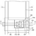
도 1은 본 발명의 한 실시예에 따른 박막 트랜지스터 표시판을 나타내는 평면도이다.
도 2는 도 1의 절단선 II-II를 따라 자른 단면도이다.
도 3은 본 발명의 다른 실시예에 따른 박막 트랜지스터 표시판을 나타내는 평면도이다.
도 4는 본 발명의 또 다른 실시예에 따른 박막 트랜지스터 표시판을 나타내는 평면도이다.
도 5는 도 4의 절단선 V-V를 따라 자른 단면도이다.
도 6은 본 발명의 또 다른 실시예에 따른 박막 트랜지스터 표시판을 나타내는 평면도이다.
도 7은 본 발명의 또 다른 실시예에 따른 박막 트랜지스터 표시판을 나타내는 평면도이다.
도 8은 본 발명의 또 다른 실시예에 따른 박막 트랜지스터 표시판을 나타내는 평면도이다.1 is a plan view illustrating a thin film transistor array panel according to an exemplary embodiment of the present invention.
2 is a cross-sectional view taken along line II-II in FIG.
3 is a plan view illustrating a thin film transistor array panel according to another exemplary embodiment of the present invention.
4 is a plan view illustrating a thin film transistor array panel according to another exemplary embodiment of the present invention.
5 is a cross-sectional view taken along the cutting line VV of FIG. 4.
6 is a plan view illustrating a thin film transistor array panel according to another exemplary embodiment of the present invention.
7 is a plan view illustrating a thin film transistor array panel according to another exemplary embodiment of the present invention.
8 is a plan view illustrating a thin film transistor array panel according to another exemplary embodiment of the present invention.
첨부한 도면들을 참조하여 본 발명의 바람직한 실시예들을 상세히 설명하기로 한다. 그러나, 본 발명은 여기서 설명되는 실시예에 한정되지 않고 다른 형태로 구체화될 수도 있다. 오히려, 여기서 소개되는 실시예들은 개시된 내용이 철저하고 완전해질 수 있도록 그리고 당업자에게 본 발명의 사상이 충분히 전달될 수 있도록 하기 위해 제공되는 것이다.DETAILED DESCRIPTION OF THE PREFERRED EMBODIMENTS Reference will now be made in detail to the preferred embodiments of the present invention, examples of which are illustrated in the accompanying drawings. However, the present invention is not limited to the embodiments described herein but may be embodied in other forms. Rather, the embodiments disclosed herein are provided so that the disclosure can be thorough and complete, and will fully convey the scope of the invention to those skilled in the art.
도면들에 있어서, 층 및 영역들의 두께는 명확성을 기하기 위하여 과장된 것이다. 또한, 층이 다른 층 또는 기판 "상"에 있다고 언급되는 경우에 그것은 다른 층 또는 기판 상에 직접 형성될 수 있거나 또는 그들 사이에 제 3의 층이 개재될 수도 있다. 명세서 전체에 걸쳐서 동일한 참조번호로 표시된 부분들은 동일한 구성요소들을 의미한다.In the drawings, the thicknesses of layers and regions are exaggerated for clarity. Also, when a layer is referred to as being "on" another layer or substrate, it may be formed directly on another layer or substrate, or a third layer may be interposed therebetween. Like numbers refer to like elements throughout the specification.
도 1은 본 발명의 한 실시예에 따른 박막 트랜지스터 표시판을 나타내는 평면도이다. 도 2는 도 1의 절단선 II-II를 따라 자른 단면도이다.1 is a plan view illustrating a thin film transistor array panel according to an exemplary embodiment of the present invention. 2 is a cross-sectional view taken along line II-II in FIG.
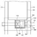
도 1을 참고하면, 본 실시예에 따른 박막 트랜지스터 표시판은 투명한 유리 또는 플라스틱 따위로 만들어진 절연 기판(110) 위에 게이트선(121)이 위치한다.Referring to FIG. 1, in the thin film transistor array panel according to the present exemplary embodiment, the
게이트선(121)은 게이트 신호를 전달하며, 주로 가로 방향으로 뻗어 있다. 각 게이트선(121)은 게이트선(121)으로부터 돌출한 게이트 전극(124)과 다른 층 또는 게이트 구동부(도시하지 않음)와의 접속을 위한 넓은 끝 부분(도시하지 않음)을 포함할 수 있다.The
게이트선(121) 및 게이트 전극(124)은 알루미늄(Al)이나 알루미늄 합금 등 알루미늄 계열 금속, 은(Ag)이나 은 합금 등 은 계열 금속, 구리(Cu), 구리망간(CuMn)과 같은 구리 합금 등 구리 계열 금속, 몰리브덴(Mo)이나 몰리브덴 합금 등 몰리브덴 계열 금속, 크롬(Cr), 탄탈륨(Ta) 및 티타늄(Ti) 등을 포함할 수 있다. 또는 게이트선(121) 및 게이트 전극(124)은 ITO(indium tin oxide), IZO(indium zinc oxide), AZO(aluminium doped ZnO) 등의 투명성 도전 물질을 포함할 수도 있다.The
본 실시예에서는 게이트선(121) 및 게이트 전극(124)이 단일막으로 형성되는 것으로 설명하였으나, 이에 한정되지 않고 이중막 또는 삼중막 형태 등으로 형성될 수 있다.In the present exemplary embodiment, the
이중막 구조를 갖는 경우, 게이트선(121) 및 게이트 전극(124)은 하부막 및 상부막으로 형성될 수 있고, 하부막은 몰리브덴(Mo)과 몰리브덴 합금 등 몰리브덴 계열의 금속, 크롬(Cr), 크롬 합금, 티타늄(Ti), 티타늄 합금, 탄탈늄(Ta), 탄탈늄 합금, 망간(Mn), 망간 합금 중에서 선택된 하나로 이루어질 수 있다. 상부막은 알루미늄(Al)과 알루미늄 합금 등 알루미늄 계열의 금속, 은(Ag)과 은 합금 등 은 계열의 금속, 구리(Cu)와 구리 합금 등 구리 계열의 금속 중 선택된 하나로 이루어질 수 있다. 삼중막 구조의 경우, 서로 물리적 성질이 다른 막들이 조합되어 형성될 수 있다In the case of the double layer structure, the
게이트선(121) 및 게이트 전극(124) 위에 게이트 절연막(140)이 위치한다. 게이트 절연막(140)은 질화규소(SiNx), 산화규소(SiOx), 산질화 규소(silicon oxynitride; SiON), 유기 절연 물질 등을 포함할 수 있다. 게이트 절연막(140)은 두 개 이상의 절연막(도시하지 않음)을 포함하는 다중막 구조를 가질 수도 있다. 예를 들어, 게이트 절연막(140)의 상층부는 산화규소(SiOx), 하층부는 질화규소(SiNx)일 수 있으며, 또는 상층부는 산화규소(SiOx), 하층부는 산질화 규소(silicon oxynitride; SiON)일 수 있다. 이 후 설명하는 반도체층(154)이 산화물 반도체로 형성되는 경우, 산화물 반도체와 접촉하는 게이트 절연막(140)이 산화물을 포함하는 경우, 채널층의 열화를 방지할 수 있다.The
게이트 절연막(140) 위에는 반도체층(151, 154)이 형성되어 있다. 반도체층(151, 154)은 데이터선(171) 하부에서 세로 방향으로 뻗어 있는 선형 부분(151)과, 게이트 전극(124)을 향하여 뻗어 나온 돌출부(projection; 154)를 포함한다.The semiconductor layers 151 and 154 are formed on the
반도체층(151, 154)은 비정질 실리콘, 결정질 실리콘 또는 산화물 반도체로 형성될 수 있다.The semiconductor layers 151 and 154 may be formed of amorphous silicon, crystalline silicon, or oxide semiconductors.
반도체층(151, 154) 위에 소스 전극(173)을 포함하는 데이터선(171) 및 드레인 전극(175)이 서로 이격되어 위치한다. 데이터선(171)은 데이터 신호를 전달하며 주로 세로 방향으로 뻗어 게이트선(121)과 교차한다.The
데이터선(171), 소스 전극(173) 및 드레인 전극(175)은 알루미늄이나 알루미늄 합금 등 알루미늄 계열 금속, 은이나 은 합금 등 은 계열 금속, 구리나 구리망간과 같은 구리 합금 등 구리 계열 금속, 몰리브덴이나 몰리브덴 합금 등 몰리브덴 계열 금속, 크롬, 탄탈륨 및 티타늄 따위로 만들어질 수 있다. 예를 들어, 몰리브덴 합금으로 Mo-Nb, Mo-Ti가 있다. 또는 데이터선(171), 소스 전극(173) 및 드레인 전극(175)은 ITO, IZO, AZO 등의 투명성 도전 물질로 만들어질 수도 있다. 데이터선(171), 소스 전극(173) 및 드레인 전극(175)은 두 개 이상의 도전막(도시하지 않음)을 포함하는 다중막 구조를 가질 수도 있다. 예를 들어, Mo/Al/Mo, Mo/Al, Mo/Cu, CuMn/Cu, Ti/Cu 등이 있다.The
본 실시예에서는 소스 전극(173)이 데이터선(171)의 일부분으로 세로 방향으로 뻗은 데이터선(171)의 연장선 상에 위치하는 것으로 설명하였으나, 데이터선(171)으로부터 돌출되어 U자 형상을 가지도록 형성할 수 있다. 물론, U자 형상은 다양한 형태로 변형 가능하다.In the present exemplary embodiment, the
반도체층의 돌출부(154)에서 소스 전극(173)과 드레인 전극(175) 사이에 소스 전극(173) 및 드레인 전극(175)으로 가리지 않고 노출된 부분이 있다. 이 부분은 박막 트랜지스터의 채널부를 형성할 수 있다. 반도체층(151, 154)은 반도체층(154)의 채널부를 제외하고, 소스 전극(173) 및 드레인 전극(175)과 실질적으로 동일한 평면 패턴을 가질 수 있다.An exposed portion of the
하나의 게이트 전극(124), 하나의 소스 전극(173) 및 하나의 드레인 전극(175)은 산화물 반도체층(154)과 함께 하나의 박막 트랜지스터(thin film transistor, TFT)를 이루며, 박막 트랜지스터의 채널은 소스 전극(173)과 드레인 전극(175) 사이에 형성된다.One
본 실시예에서 박막 트랜지스터의 채널부(CH)는 가로 방향으로 뻗어 있는 게이트선(121)의 연장선 상에 위치한다. 게이트선(121)이 가로 방향으로 뻗으면서 채널부(CH)와 교차하는 모양이다. 채널부(CH)는 게이트선(121)으로부터 돌출된 게이트 전극(124)과 일부 중첩할 수 있다.In the present exemplary embodiment, the channel portion CH of the thin film transistor is positioned on an extension line of the
그리고, 본 실시예에서 드레인 전극(175)은 박막 트랜지스터의 채널부(CH)와 마찬가지로 게이트선(121)이 뻗어 있는 연장선 상에 위치한다.In the present embodiment, the
드레인 전극(175)은 게이트선(121)을 중심으로 상하 대칭이 되도록 형성할 수 있다.The
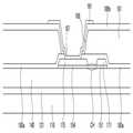
데이터선(171), 소스 전극(173), 드레인 전극(175) 및 노출된 반도체층의 돌출부(154) 부분 위에는 하부 보호막(180a)이 형성되어 있다. 하부 보호막(180a)은 질화 규소나 산화 규소 따위의 무기 절연물로 형성할 수 있다.The
하부 보호막(180a)은 드레인 전극(175) 일부를 드러내는 제1 접촉 구멍(187)을 갖는다. 본 실시예에서 제 1 접촉 구멍(187)은 도 1에 도시한 바와 같이 게이트선(121)이 뻗어 있는 연장선 상에 위치한다.The
이처럼 본 실시예에서 반도체층(151, 154)의 채널부(CH)와 제1 접촉 구멍(187)을 게이트선(121)이 뻗어 있는 연장선 상에 형성함으로써 박막 트랜지스터의 드레인 영역과 제1 접촉 구멍(187)이 형성되는 드레인 전극(175) 부분을 연결하는 전극 구성 부분을 생략할 수 있다. 따라서, 마진을 고려하여 드레인 전극을 형성하기 위한 가로 사이즈 등을 줄일 수 있는 구조이기 때문에 화소 크기를 줄일 수 있다.As described above, in the present embodiment, the channel portion CH and the
이처럼 본 실시예에서 반도체층(151, 154)의 채널부(CH)와 제1 접촉 구멍(187)을 게이트선(121)이 뻗어 있는 연장선 상에 형성함으로써 차광 부재(BM)의 폭(D1)을 감소시켜 개구율을 증가시킬 수 있다. 차광 부재(BM)는 빛샘을 방지하기 위해 형성하는 것으로 블랙 매트릭스라고도 한다. 차광 부재(BM)는 게이트선(121)을 중심으로 상하 대칭으로 형성할 수 있다.As such, in the present embodiment, the channel portion CH and the
본 실시예에서 드레인 전극(175)이 게이트선(121)과 중첩하기 때문에 게이트-드레인 기생 용량이 증가할 수 있으나, 반도체층(151, 154)을 산화물 반도체로 형성하게 되면 구동 전압을 낮출 수 있기 때문에 기생 용량 증가를 최소화할 수 있다. 본 실시예에서 반도체층(151, 154)은 산화물 반도체로 형성하는 것이 바람직하다.In the present embodiment, since the
본 실시예에서 반도체층(151, 154)의 평면 모양은 채널부(CH) 이외의 부분에서 소스 전극(173)을 포함하는 데이터선(171) 및 드레인 전극(175)을 포함하는 평면 모양과 동일할 수 있다.In this embodiment, the planar shape of the semiconductor layers 151 and 154 is the same as the planar shape including the
하부 보호막(180a) 위에 제2 접촉 구멍(188)을 갖는 유기 절연막(181)과 상부 보호막(180b)이 위치할 수 있다. 제2 접촉 구멍(188)은 제1 접촉 구멍(187)보다 넓게 형성될 수 있고, 상부 보호막(180b)은 하부 보호막(180a)과 유사하게 질화 규소나 산화 규소 따위의 무기 절연물로 형성할 수 있다. 유기 절연막(181)과 상부 보호막(180b)은 생략될 수 있다.The organic insulating
상부 보호막(180b) 위에 화소 전극(191)이 위치한다. 화소 전극(191)은 접촉 구멍(187, 188)을 통하여 드레인 전극(175)과 물리적, 전기적으로 연결되어 있으며, 드레인 전극(175)으로부터 데이터 전압을 인가 받는다. 화소 전극(191)은 ITO, IZO 등을 포함하는 투명한 도전성 산화물을 포함할 수 있다.The
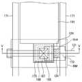
도 3은 본 발명의 다른 실시예에 따른 박막 트랜지스터 표시판을 나타내는 평면도이다.3 is a plan view illustrating a thin film transistor array panel according to another exemplary embodiment of the present invention.
도 3의 실시예는, 도 1 및 도 2에서 설명한 실시예와 대부분 동일하고, 이하 차이가 있는 부분에 대해 설명하기로 한다.The embodiment of FIG. 3 is mostly the same as the embodiment described with reference to FIGS. 1 and 2 and will be described below with differences.
도 3을 참고하면, 도 1의 실시예와 달리 게이트 전극(124)이 형성되지 않고, 게이트선(121)은 가로 방향을 따라 실질적으로 동일한 폭을 가지면서 뻗어 있다. 이 때, 소스 전극(173) 및 드레인 전극(175)으로 가리지 않고 노출된 부분이 게이트선(121) 폭보다 넓게 형성되더라도 게이트 전극(121)이 형성되지 않기 때문에 게이트선(121)과 중첩하는 반도체층의 돌출부(154)의 세로 방향의 폭은 반도체층의 돌출부(154)의 폭보다 작다. 다시 말해, 채널부(CH)의 폭은 게이트선(121)의 폭과 동일하게 형성된다.Referring to FIG. 3, unlike the embodiment of FIG. 1, the
또한, 반도체층의 돌출부(154)를 게이트선(121)과 완전히 중첩하는 형태로 형성할 수 있고, 이 경우에는 어느 정도 오정렬(mis-align)이 발생하더라도 채널부(CH)의 폭은 일정하게 유지될 수 있다.In addition, the
본 실시예에 따르면 게이트 전극(124)을 형성하지 않기 때문에 게이트선(121)과 소스 전극(173) 또는 드레인 전극(175)이 중첩하는 면적이 줄어들기 때문에 게이트와 소스 또는 게이트와 드레인 사이에 발생할 수 있는 기생 용량을 줄일 수 있다.According to the present exemplary embodiment, since the
도 1의 실시예와 차이가 있는 부분을 제외하고 도 1의 실시예에서 설명한 내용들은 도 3의 실시예에 적용될 수 있다.Except for parts that differ from the embodiment of FIG. 1, the contents described in the embodiment of FIG. 1 may be applied to the embodiment of FIG. 3.
도 4는 본 발명의 또 다른 실시예에 따른 박막 트랜지스터 표시판을 나타내는 평면도이다. 도 5는 도 4의 절단선 V-V를 따라 자른 단면도이다.4 is a plan view illustrating a thin film transistor array panel according to another exemplary embodiment of the present invention. 5 is a cross-sectional view taken along the line V-V of FIG. 4.
도 4 및 도 5의 실시예는 도 1의 실시예와 대부분 동일하고, 이하 차이가 있는 부분에 대해 설명하기로 한다.4 and 5 are substantially the same as the embodiment of FIG. 1, and differences will be described below.
도 4 및 도 5를 참고하면, 드레인 전극(175)에 반도체층의 돌출부(154) 일부를 드러내는 개구부(185)가 형성되어 있다. 개구부(185)는 하부 보호막(180a)이 갖는 제1 접촉 구멍(187)보다 작게 형성될 수 있다. 개구부(185)에 의해 노출된 반도체층의 돌출부(154)는 절연 특성을 갖는 절연부(154I)일 수 있다. 절연부(154I)를 형성하기 위해 개구부(185)에 의해 노출된 드레인 전극(175) 부분을 플라즈마 처리할 수 있다. 플라즈마 처리는 산소 플라즈마 처리를 포함할 수 있고, 하부 보호막(180a), 유기 절연막(180), 상부 보호막(180b)에 대한 패터닝 이후에 후처리 과정으로 진행할 수 있다. 따라서, 절연부(154I)가 반도체나 메탈 특성을 갖지 않도록 할 수 있다.4 and 5, an
본 실시예에 따르면, 게이트선(121)과 중첩하는 드레인 전극(175) 부분을 줄임으로써 게이트와 드레인 사이에 발생할 수 있는 기생 용량을 보다 줄이는 효과가 있다. 그리고, 개구부(185)가 형성됨으로써 화소 전극(191)과 반도체층의 돌출부(154)가 직접 접촉하는 문제가 발생할 수 있으나, 반도체층의 돌출부(154)에 절연부(154I)를 형성함으로써, 화소 전극과 반도체층(154)가 쇼트되지 않도록 한다.According to the present exemplary embodiment, parasitic capacitance that may occur between the gate and the drain may be further reduced by reducing the portion of the
본 실시예에서 개구부(185)의 모양은 제1 접촉 구멍(187)와 유사한 사각형이고, 제1 접촉 구멍(187) 가운데에 위치한다. 따라서, 화소 전극(191)은 반도체층의 돌출부(154) 중에서 절연부(154I)와 접촉하면서 동시에 제1 접촉 구멍의 가장 자리 부분에서 노출되어 있는 드레인 전극(175) 부분과 접촉한다.In this embodiment, the shape of the
도 1의 실시예와 차이가 있는 부분을 제외하고 도 1의 실시예에서 설명한 내용들은 도 4 및 도 5의 실시예에 적용될 수 있다.Except for parts that differ from the embodiment of FIG. 1, the contents described in the embodiment of FIG. 1 may be applied to the embodiments of FIGS. 4 and 5.
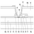
도 6 및 도 7은 본 발명의 또 다른 실시예에 따른 박막 트랜지스터 표시판을 나타내는 평면도이다.6 and 7 are plan views illustrating a thin film transistor array panel according to another exemplary embodiment of the present invention.
도 6 및 도 7의 실시예는 도 4의 실시예에서 개구부(185)의 모양 또는 위치를 변형한 것이다. 따라서, 차이가 있는 부분에 대해서만 설명하기로 하고, 도 4 및 도 5의 실시예에서 설명한 내용은 대부분 본 실시예에 적용할 수 있다.6 and 7 modify the shape or position of the
도 6을 참고하면, 개구부(175)가 제1 접촉 구멍(187)의 왼쪽 변을 중심으로 위치한다. 따라서, 화소 전극(191)은 제1 접촉 구멍(187) 내에서 오른쪽 부분에 위치하는 드레인 전극(175)과 주로 접촉한다.Referring to FIG. 6, the
도 7을 참고하면, 개구부(175)가 제1 접촉 구멍(187)의 가운데 부분을 중심으로 세로 방향으로 긴 직사각형 형태로 형성되어 있다. 따라서, 화소 전극(191)은 제1 접촉 구멍(187)의 좌우 가장자리 부분에 위치하는 드레인 전극(175)과 접촉할 수 있다.Referring to FIG. 7, the
도 6 및 도 7의 실시예에서 개구부(185)의 위치 및 모양에 대한 실시예를 설명하였으나, 이에 한정되지 않고 화소 전극(191)과 드레인 전극(175)이 전기적, 물질적으로 연결 가능하게 하는 범위에서 드레인 전극(175) 일부를 패터닝할 수 있다면 개구부(185)의 위치 및 모양은 다양하게 변형 가능하다.6 and 7 illustrate embodiments of the position and shape of the
도 8은 본 발명의 또 다른 실시예에 따른 박막 트랜지스터 표시판을 나타내는 평면도이다.8 is a plan view illustrating a thin film transistor array panel according to another exemplary embodiment of the present invention.
도 8은 도 3의 실시예를 변형한 형태로 차이가 있는 부분에 대해서 설명하기로 한다.8 will be described with respect to the difference in the form of the embodiment of FIG.
도 8을 참고하면, 도 3의 실시예와 마찬가지로 박막 트랜지스터의 채널부(CH) 및 제1 접촉 구멍(187)이 게이트선(121)과 중첩한다. 도 3의 실시예와 달리 본 실시예에의 게이트선(121)은 일부 꺾인 부분을 포함한다. 게이트선(121)의 꺾인 부분은 채널부(CH)과 채널부(CH)에서 멀리 떨어진 데이터선(171) 사이에 형성된다. 이와 같이 채널부(CH)와 차광 부재(BM)의 거리(D3)를 약간 늘림으로써 오정렬이 발생하여 채널부(CH)가 차광 부재(BM) 밖으로 노출될 가능성을 줄일 수 있다.Referring to FIG. 8, similar to the embodiment of FIG. 3, the channel portion CH and the
이하에서는 본 발명의 박막 트랜지스터 표시판을 제조하는 방법에 대해 도 4 및 도 5를 참고하여 간단히 설명하기로 한다.Hereinafter, a method of manufacturing the thin film transistor array panel of the present invention will be briefly described with reference to FIGS. 4 and 5.
기판(110) 위에 가로 방향으로 뻗어 있는 게이트선(121)을 형성한다. 실시예에 따라서 게이트선(121)으로부터 돌출된 게이트 전극(124)을 형성할 수도 있고 생략할 수도 있다.A
게이트선(121) 위에 게이트 절연막(140)을 형성하고, 게이트 절연막(140) 위에 세로 방향으로 뻗어 있는 선형 부분(151)과, 게이트 전극(124)을 향하여 뻗어 나온 돌출부(projection; 154)를 포함하는 반도체층(151, 154)을 형성한다.The
반도체층(151, 154) 위에 세로 방향으로 뻗으면서 게이트선(121)과 교차하는 데이터선(171)을 형성한다. 게이트선(121)과 교차하는 데이터선(171) 부분은 소스 전극(173)을 형성하고, 채널부(CH)를 중심으로 소스 전극(175)과 이격된 위치에 드레인 전극(175)을 형성한다. 드레인 전극(175)은 게이트선(121)이 뻗어 있는 연장선 상에 위치하도록 형성할 수 있다.A
본 실시예에서는 소스 전극(173)이 데이터선(171)의 일부로 형성하는 것으로 설명하였으나, 데이터선(171)으로부터 돌출되어 U자 형상을 가지도록 형성할 수 있다. 물론, U자 형상은 다양한 형태로 변형 가능하다.In the present exemplary embodiment, the
데이터선(171), 소스 전극(173), 드레인 전극(175) 및 노출된 반도체층의 돌출부(154) 부분 위에 무기 절연 물질 또는 유기 물질 등을 증착한 후 패터닝하여 제1 접촉 구멍(187)을 갖는 하부 보호막(180a), 제2 접촉 구멍(188)을 갖는 유기 절연막(181)을 형성한다. 하부 보호막(180a), 유기 절연막(181) 위에 무기 절연 물질 등을 증착한 후에 패터닝하여 상부 보호막(180b)을 형성할 수 있다. 상부 보호막(180b)은 제1 접촉 구멍(187)과 중첩하는 형태로 접촉 구멍(미도시)을 포함할 수 있다.The
하부 보호막(180a), 유기 절연막(181) 및 상부 보호막(180b)의 증착 및 패터닝하는 순서는 다양하게 변형 가능하다. 여기서, 유기 절연막(181), 상부 보호막(180b)은 형성하지 않을 수 있다.The order of depositing and patterning the
본 실시예에서 하부 보호막(180a)을 형성하는 과정에서 드레인 전극(175) 일부가 노출된다. 이 때, 노출된 드레인 전극(175) 일부를 패터닝하여 개구부(185)를 형성하고, 개구부(185)에 의해 반도체층의 돌출부(154)를 노출한다. 노출된 반도체층의 돌출부(154)를 플라즈마 처리하여 절연부(154I)를 형성한다. 플라즈마 처리는 산소 플라즈마 처리를 포함할 수 있다. 이처럼, 플라즈마 처리된 절연부(154I)는 반도체 및 메탈 특성이 약해져 절연 특성을 갖는다.In the present embodiment, a portion of the
개구부(185)의 넓이는 제1 접촉 구멍(187)의 넓이보다 작게 형성한다.The width of the
개구부(185), 제1 접촉 구멍(187), 제2 접촉 구멍(188) 및 상부 보호막(180b)이 갖는 접촉 구멍(미도시)을 채우도록 화소 전극 물질을 증착한 후에 패터닝하여 화소 전극(191)을 형성한다.The
본 실시예에 따른 박막 트랜지스터 표시판 제조 방법은 도 4의 실시예에 따른 박막 트랜지스터 표시판을 제조하는 것을 중심으로 설명하였으나, 다른 실시예에 따른 박막 트랜지스터 표시판을 형성하기 위해 변형 가능하다.The method of manufacturing the thin film transistor array panel according to the present exemplary embodiment has been described with reference to manufacturing the thin film transistor array panel according to the exemplary embodiment of FIG. 4, but may be modified to form the thin film transistor array panel according to another exemplary embodiment.
이상에서 본 발명의 바람직한 실시예에 대하여 상세하게 설명하였지만 본 발명의 권리범위는 이에 한정되는 것은 아니고 다음의 청구범위에서 정의하고 있는 본 발명의 기본 개념을 이용한 당업자의 여러 변형 및 개량 형태 또한 본 발명의 권리범위에 속하는 것이다.Although the preferred embodiments of the present invention have been described in detail above, the scope of the present invention is not limited thereto, and various modifications and improvements of those skilled in the art using the basic concepts of the present invention defined in the following claims are also provided. It belongs to the scope of right.
110기판121게이트선
124게이트 전극140게이트 절연막
151, 154반도체층 173소스 전극
175드레인 전극185개구부
187제1 접촉 구멍191화소 전극110
124
151, 154
175
187
Claims (20)
Translated fromKorean상기 기판 위에 위치하는 게이트선,
상기 게이트선 위에 위치하는 게이트 절연막,
상기 게이트 절연막 위에 위치하는 반도체층,
상기 반도체층 위에 위치하는 소스 전극을 포함하는 데이터선 및 드레인 전극,
상기 데이터선 및 상기 드레인 전극 위에 위치하고, 접촉 구멍을 갖는 보호막 그리고
상기 보호막 위에 위치하는 화소 전극을 포함하고,
상기 접촉 구멍은 상기 화소 전극과 상기 드레인 전극을 연결하고,
상기 반도체층의 채널부 및 상기 접촉 구멍은 상기 게이트선이 뻗어 있는 연장선 상에 위치하는 박막 트랜지스터 표시판.Board,
A gate line positioned on the substrate,
A gate insulating film disposed on the gate line,
A semiconductor layer on the gate insulating layer,
A data line and a drain electrode including a source electrode on the semiconductor layer;
A passivation layer on the data line and the drain electrode and having a contact hole;
A pixel electrode on the passivation layer,
The contact hole connects the pixel electrode and the drain electrode,
The channel portion and the contact hole of the semiconductor layer are positioned on an extension line in which the gate line extends.
상기 게이트선은 상기 게이트선이 뻗어 있는 연장선에서 돌출되어 형성된 게이트 전극을 포함하는 박막 트랜지스터 표시판.In claim 1,
The gate line includes a gate electrode protruding from an extension line in which the gate line extends.
상기 소스 전극은 상기 게이트선과 중첩하는 박막 트랜지스터 표시판.3. The method of claim 2,
And the source electrode overlaps the gate line.
상기 드레인 전극은 상기 게이트선과 중첩하고, 상기 게이트선을 중심으로 상하 대칭인 박막 트랜지스터 표시판.4. The method of claim 3,
The drain electrode overlaps the gate line and is vertically symmetric with respect to the gate line.
상기 반도체층의 채널부 폭은 상기 게이트선의 폭과 동일한 박막 트랜지스터 표시판.In claim 1,
The channel portion width of the semiconductor layer is the same as that of the gate line.
상기 소스 전극은 상기 게이트선과 중첩하는 박막 트랜지스터 표시판.The method of claim 5,
And the source electrode overlaps the gate line.
상기 드레인 전극은 상기 게이트선과 중첩하고, 상기 게이트선을 중심으로 상하 대칭인 박막 트랜지스터 표시판.The method of claim 6,
The drain electrode overlaps the gate line and is vertically symmetric with respect to the gate line.
상기 드레인 전극은 상기 반도체층 일부를 드러내는 개구부를 포함하는 박막 트랜지스터 표시판.In claim 1,
The drain electrode may include an opening that exposes a portion of the semiconductor layer.
상기 개구부에 의해 드러난 상기 반도체층 부분은 절연 특성을 갖는 박막 트랜지스터 표시판.9. The method of claim 8,
The semiconductor layer portion exposed by the opening has an insulating property.
상기 개구부의 넓이는 상기 접촉 구멍의 넓이보다 작은 박막 트랜지스터 표시판.The method of claim 9,
The thin film transistor array panel of which the width of the opening is smaller than the width of the contact hole.
상기 게이트선은 상기 게이트선이 뻗어 있는 연장선 상에서 벗어난 꺾인 부분을 포함하는 박막 트랜지스터 표시판.11. The method of claim 10,
And the gate line includes a bent portion that is out of an extension line on which the gate line extends.
상기 기판 위에 위치하는 차광 부재를 더 포함하고,
상기 차광 부재는 상기 드레인 전극을 완전히 덮고, 상기 게이트선을 중심으로 상하 대칭인 박막 트랜지스터 표시판.In claim 1,
Further comprising a light shielding member located on the substrate,
The light blocking member completely covers the drain electrode and is vertically symmetrical with respect to the gate line.
상기 반도체층의 평면 모양은 상기 채널부 이외의 부분에서 상기 소스 전극을 포함하는 상기 데이터선 및 상기 드레인 전극을 포함하는 평면 모양과 동일한 박막 트랜지스터 표시판.In claim 1,
The planar shape of the semiconductor layer is the same as that of the planar shape including the data line and the drain electrode including the source electrode in portions other than the channel portion.
상기 반도체층은 산화물 반도체로 형성하는 박막 트랜지스터 표시판.In claim 1,
And the semiconductor layer is formed of an oxide semiconductor.
상기 게이트선 위에 게이트 절연막을 형성하는 단계,
상기 게이트 절연막 위에 반도체층을 형성하는 단계,
상기 반도체층 위에 소스 전극을 포함하는 데이터선 및 드레인 전극을 형성하는 단계,
상기 데이터선 및 상기 드레인 전극 위에 절연 물질을 증착하는 단계,
상기 절연 물질을 패터닝하여 접촉 구멍을 갖는 보호막을 형성하는 단계 그리고
상기 보호막 위에 상기 접촉 구멍을 통해 상기 드레인 전극과 연결되는 화소 전극을 형성하는 단계를 포함하고,
상기 반도체층의 채널부 및 상기 접촉 구멍은 상기 게이트선이 뻗어 있는 연장선 상에 형성하는 박막 트랜지스터 표시판 제조 방법.Forming a gate line on the substrate,
Forming a gate insulating film on the gate line,
Forming a semiconductor layer on the gate insulating film,
Forming a data line and a drain electrode including a source electrode on the semiconductor layer;
Depositing an insulating material on the data line and the drain electrode;
Patterning the insulating material to form a protective film having a contact hole; and
Forming a pixel electrode on the passivation layer and connected to the drain electrode through the contact hole;
The channel portion and the contact hole of the semiconductor layer are formed on an extension line on which the gate line extends.
상기 접촉 구멍에 의해 노출되는 상기 드레인 전극을 패터닝하여 개구부를 형성하는 단계를 더 포함하는 박막 트랜지스터 표시판 제조 방법.16. The method of claim 15,
And forming an opening by patterning the drain electrode exposed by the contact hole.
상기 개구부에 의해 드러나는 상기 반도체층 부분을 플라즈마 처리하는 단계를 더 포함하는 박막 트랜지스터 표시판 제조 방법.17. The method of claim 16,
And plasma processing the portion of the semiconductor layer exposed by the opening.
상기 플라즈마 처리된 반도체층 부분은 절연 특성을 갖는 박막 트랜지스터 표시판 제조 방법.The method of claim 17,
The plasma treated semiconductor layer portion has a thin film transistor display panel having an insulating property.
상기 플라즈마 처리하는 단계는 산소 플라즈마 처리하는 박막 트랜지스터 표시판 제조 방법.In paragraph 18,
The plasma treatment may be performed by performing an oxygen plasma treatment.
상기 개구부를 형성하는 단계에서 상기 개구부의 넓이는 상기 접촉 구멍의 넓이보다 작게 형성하는 박막 트랜지스터 표시판 제조 방법.17. The method of claim 16,
And forming a width of the opening smaller than that of the contact hole.
Priority Applications (2)
| Application Number | Priority Date | Filing Date | Title |
|---|---|---|---|
| KR1020120053719AKR101987985B1 (en) | 2012-05-21 | 2012-05-21 | Thin film transistor array panel and method for manufacturing the same |
| US13/725,333US9142680B2 (en) | 2012-05-21 | 2012-12-21 | Thin film transistor array panel having improved aperture ratio and method of manufacturing same |
Applications Claiming Priority (1)
| Application Number | Priority Date | Filing Date | Title |
|---|---|---|---|
| KR1020120053719AKR101987985B1 (en) | 2012-05-21 | 2012-05-21 | Thin film transistor array panel and method for manufacturing the same |
Publications (2)
| Publication Number | Publication Date |
|---|---|
| KR20130129673Atrue KR20130129673A (en) | 2013-11-29 |
| KR101987985B1 KR101987985B1 (en) | 2019-10-01 |
Family
ID=49580584
Family Applications (1)
| Application Number | Title | Priority Date | Filing Date |
|---|---|---|---|
| KR1020120053719AActiveKR101987985B1 (en) | 2012-05-21 | 2012-05-21 | Thin film transistor array panel and method for manufacturing the same |
Country Status (2)
| Country | Link |
|---|---|
| US (1) | US9142680B2 (en) |
| KR (1) | KR101987985B1 (en) |
Cited By (1)
| Publication number | Priority date | Publication date | Assignee | Title |
|---|---|---|---|---|
| US9012994B2 (en) | 2013-05-08 | 2015-04-21 | Samsung Display Co., Ltd. | Thin film transistor array panel and method for manufacturing the same |
Families Citing this family (5)
| Publication number | Priority date | Publication date | Assignee | Title |
|---|---|---|---|---|
| TWI483036B (en) | 2012-11-19 | 2015-05-01 | Au Optronics Corp | Array substrate and manufacturing method thereof |
| CN103178119B (en)* | 2013-03-25 | 2015-07-29 | 京东方科技集团股份有限公司 | Array base palte, array base palte preparation method and display unit |
| CN103676354B (en)* | 2013-12-06 | 2016-03-23 | 合肥京东方光电科技有限公司 | Electrode structure and preparation method, array base palte and preparation method and display device |
| KR20160066580A (en)* | 2014-12-02 | 2016-06-13 | 삼성디스플레이 주식회사 | Display device |
| CN110707096A (en)* | 2019-09-18 | 2020-01-17 | 深圳市华星光电半导体显示技术有限公司 | Array substrate, preparation method thereof and display device |
Citations (6)
| Publication number | Priority date | Publication date | Assignee | Title |
|---|---|---|---|---|
| JP2002365665A (en)* | 2001-06-08 | 2002-12-18 | Nec Kagoshima Ltd | Active matrix type liquid crystal display device and its manufacturing method |
| KR20030053241A (en)* | 2001-12-22 | 2003-06-28 | 엘지.필립스 엘시디 주식회사 | Liquid Crystal Display Device and method for manufacturing the same |
| JP2004158518A (en)* | 2002-11-05 | 2004-06-03 | Sharp Corp | Active matrix substrate and display device |
| JP2006191016A (en)* | 2004-12-30 | 2006-07-20 | Lg Philips Lcd Co Ltd | Thin film transistor array substrate and manufacturing method thereof |
| KR20070070718A (en)* | 2005-12-29 | 2007-07-04 | 엘지.필립스 엘시디 주식회사 | Method of manufacturing thin film transistor substrate |
| JP2010080952A (en)* | 2008-09-01 | 2010-04-08 | Semiconductor Energy Lab Co Ltd | Semiconductor device and method for manufacturing the same |
Family Cites Families (18)
| Publication number | Priority date | Publication date | Assignee | Title |
|---|---|---|---|---|
| KR100560974B1 (en) | 1998-11-26 | 2006-09-06 | 삼성전자주식회사 | Thin film transistor substrate for liquid crystal display device and manufacturing method thereof |
| KR100672648B1 (en) | 2004-12-14 | 2007-01-24 | 엘지.필립스 엘시디 주식회사 | Liquid crystal display and manufacturing method thereof |
| KR101107682B1 (en)* | 2004-12-31 | 2012-01-25 | 엘지디스플레이 주식회사 | Thin film transistor substrate for display element and manufacturing method thereof |
| KR20070081016A (en)* | 2006-02-09 | 2007-08-14 | 삼성전자주식회사 | Thin film transistor array panel and manufacturing method thereof |
| US8059329B2 (en)* | 2006-10-04 | 2011-11-15 | Samsung Electronics Co., Ltd. | Display substrate and method of manufacturing the same |
| KR101410926B1 (en)* | 2007-02-16 | 2014-06-24 | 삼성전자주식회사 | Thin film transistor and manufacturing method thereof |
| JP2009128577A (en) | 2007-11-22 | 2009-06-11 | Hitachi Ltd | Organic light emitting display |
| KR20090129805A (en) | 2008-06-13 | 2009-12-17 | 엘지디스플레이 주식회사 | Array board for transverse electric field type liquid crystal display |
| KR20100065876A (en) | 2008-12-09 | 2010-06-17 | 삼성전자주식회사 | Liquid crystal device and method for manufacturing the same |
| US8232947B2 (en)* | 2008-11-14 | 2012-07-31 | Semiconductor Energy Laboratory Co., Ltd. | Liquid crystal display device |
| KR101101021B1 (en) | 2009-10-09 | 2011-12-29 | 삼성모바일디스플레이주식회사 | Liquid crystal display device and manufacturing method thereof |
| KR101101007B1 (en) | 2009-10-09 | 2011-12-29 | 삼성모바일디스플레이주식회사 | LCD Display |
| KR20110041139A (en) | 2009-10-15 | 2011-04-21 | 삼성모바일디스플레이주식회사 | Liquid crystal display device and manufacturing method thereof |
| KR101588448B1 (en) | 2009-12-03 | 2016-01-25 | 엘지디스플레이 주식회사 | Array substrate including thin film transistor using polysilicon and manufacturing method thereof |
| US8791463B2 (en)* | 2010-04-21 | 2014-07-29 | Sharp Kabushiki Kaisha | Thin-film transistor substrate |
| JP5776967B2 (en)* | 2010-06-11 | 2015-09-09 | Nltテクノロジー株式会社 | Image display device, driving method of image display device, and terminal device |
| KR20120000254A (en) | 2010-06-25 | 2012-01-02 | 엘지디스플레이 주식회사 | Indirect thermal crystallization thin film transistor substrate and manufacturing method thereof |
| KR20120007764A (en) | 2010-07-15 | 2012-01-25 | 엘지디스플레이 주식회사 | Array substrate including thin film transistor using micro polysilicon and manufacturing method thereof |
- 2012
- 2012-05-21KRKR1020120053719Apatent/KR101987985B1/enactiveActive
- 2012-12-21USUS13/725,333patent/US9142680B2/enactiveActive
Patent Citations (6)
| Publication number | Priority date | Publication date | Assignee | Title |
|---|---|---|---|---|
| JP2002365665A (en)* | 2001-06-08 | 2002-12-18 | Nec Kagoshima Ltd | Active matrix type liquid crystal display device and its manufacturing method |
| KR20030053241A (en)* | 2001-12-22 | 2003-06-28 | 엘지.필립스 엘시디 주식회사 | Liquid Crystal Display Device and method for manufacturing the same |
| JP2004158518A (en)* | 2002-11-05 | 2004-06-03 | Sharp Corp | Active matrix substrate and display device |
| JP2006191016A (en)* | 2004-12-30 | 2006-07-20 | Lg Philips Lcd Co Ltd | Thin film transistor array substrate and manufacturing method thereof |
| KR20070070718A (en)* | 2005-12-29 | 2007-07-04 | 엘지.필립스 엘시디 주식회사 | Method of manufacturing thin film transistor substrate |
| JP2010080952A (en)* | 2008-09-01 | 2010-04-08 | Semiconductor Energy Lab Co Ltd | Semiconductor device and method for manufacturing the same |
Cited By (2)
| Publication number | Priority date | Publication date | Assignee | Title |
|---|---|---|---|---|
| US9012994B2 (en) | 2013-05-08 | 2015-04-21 | Samsung Display Co., Ltd. | Thin film transistor array panel and method for manufacturing the same |
| US9281322B2 (en) | 2013-05-08 | 2016-03-08 | Samsung Display Co., Ltd. | Thin film transistor array panel and method for manufacturing the same |
Also Published As
| Publication number | Publication date |
|---|---|
| US20130306972A1 (en) | 2013-11-21 |
| KR101987985B1 (en) | 2019-10-01 |
| US9142680B2 (en) | 2015-09-22 |
Similar Documents
| Publication | Publication Date | Title |
|---|---|---|
| US7737517B2 (en) | Display device | |
| US9880436B2 (en) | Liquid crystal display device and manufacturing method thereof | |
| KR102380647B1 (en) | Thin film transistor array panel and manufacturing method thereof | |
| EP3173861B1 (en) | Liquid crystal display device and manufacturing method thereof | |
| KR102295477B1 (en) | Thin film transistor array panel | |
| KR101555113B1 (en) | Semiconductor device and process of producing same, and display device | |
| EP3621120B1 (en) | Thin film transistor and preparation method therefor, array substrate and preparation method therefor | |
| US9252160B2 (en) | Thin film transistor array panel and method of manufacturing the same | |
| KR101987985B1 (en) | Thin film transistor array panel and method for manufacturing the same | |
| KR102074424B1 (en) | Liquid crystal display and manufacturing method thereof | |
| KR101642346B1 (en) | Display substrate and display device comprising the same | |
| KR20160043576A (en) | Liquid crystal display and manufacturing method thereof | |
| US9281406B2 (en) | Thin film transistor substrate, display device including the same, and fabricating method of the thin film transistor substrate | |
| KR20120043404A (en) | Display apparatus and method of manufacturing the same | |
| KR102140644B1 (en) | Thin film transistor substrate and manufacturing method of thin film transistor substrate | |
| KR102431348B1 (en) | Display device | |
| KR20150094856A (en) | Display device and method of manufacturing display device using the same | |
| US9595542B2 (en) | Thin film transistor array panel and manufacturing method thereof | |
| US20150091011A1 (en) | Display device and method for fabricating the same | |
| KR20180063414A (en) | Display device | |
| KR102412069B1 (en) | Thin film transistor | |
| KR102228900B1 (en) | Thin film transistor array panel and manufacturing method thereof | |
| KR20160112047A (en) | Display device and manufacturing method thereof | |
| KR102390967B1 (en) | Method of manufacturing display device | |
| KR100973804B1 (en) | Thin film transistor display panel |
Legal Events
| Date | Code | Title | Description |
|---|---|---|---|
| PA0109 | Patent application | Patent event code:PA01091R01D Comment text:Patent Application Patent event date:20120521 | |
| PG1501 | Laying open of application | ||
| A201 | Request for examination | ||
| PA0201 | Request for examination | Patent event code:PA02012R01D Patent event date:20170516 Comment text:Request for Examination of Application Patent event code:PA02011R01I Patent event date:20120521 Comment text:Patent Application | |
| E902 | Notification of reason for refusal | ||
| PE0902 | Notice of grounds for rejection | Comment text:Notification of reason for refusal Patent event date:20180816 Patent event code:PE09021S01D | |
| AMND | Amendment | ||
| E601 | Decision to refuse application | ||
| PE0601 | Decision on rejection of patent | Patent event date:20190221 Comment text:Decision to Refuse Application Patent event code:PE06012S01D Patent event date:20180816 Comment text:Notification of reason for refusal Patent event code:PE06011S01I | |
| AMND | Amendment | ||
| PX0901 | Re-examination | Patent event code:PX09011S01I Patent event date:20190221 Comment text:Decision to Refuse Application Patent event code:PX09012R01I Patent event date:20181015 Comment text:Amendment to Specification, etc. | |
| PX0701 | Decision of registration after re-examination | Patent event date:20190320 Comment text:Decision to Grant Registration Patent event code:PX07013S01D Patent event date:20190318 Comment text:Amendment to Specification, etc. Patent event code:PX07012R01I Patent event date:20190221 Comment text:Decision to Refuse Application Patent event code:PX07011S01I Patent event date:20181015 Comment text:Amendment to Specification, etc. Patent event code:PX07012R01I | |
| X701 | Decision to grant (after re-examination) | ||
| GRNT | Written decision to grant | ||
| PR0701 | Registration of establishment | Comment text:Registration of Establishment Patent event date:20190604 Patent event code:PR07011E01D | |
| PR1002 | Payment of registration fee | Payment date:20190604 End annual number:3 Start annual number:1 | |
| PG1601 | Publication of registration | ||
| PR1001 | Payment of annual fee | Payment date:20220523 Start annual number:4 End annual number:4 | |
| PR1001 | Payment of annual fee | Payment date:20230524 Start annual number:5 End annual number:5 |