KR20130125717A - Semiconductor device and method for driving the same - Google Patents
Semiconductor device and method for driving the sameDownload PDFInfo
- Publication number
- KR20130125717A KR20130125717AKR1020130049086AKR20130049086AKR20130125717AKR 20130125717 AKR20130125717 AKR 20130125717AKR 1020130049086 AKR1020130049086 AKR 1020130049086AKR 20130049086 AKR20130049086 AKR 20130049086AKR 20130125717 AKR20130125717 AKR 20130125717A
- Authority
- KR
- South Korea
- Prior art keywords
- transistor
- terminal
- electrically connected
- inverting input
- electrode
- Prior art date
- Legal status (The legal status is an assumption and is not a legal conclusion. Google has not performed a legal analysis and makes no representation as to the accuracy of the status listed.)
- Ceased
Links
Images


Classifications
- H—ELECTRICITY
- H10—SEMICONDUCTOR DEVICES; ELECTRIC SOLID-STATE DEVICES NOT OTHERWISE PROVIDED FOR
- H10D—INORGANIC ELECTRIC SEMICONDUCTOR DEVICES
- H10D99/00—Subject matter not provided for in other groups of this subclass
- H—ELECTRICITY
- H03—ELECTRONIC CIRCUITRY
- H03F—AMPLIFIERS
- H03F3/00—Amplifiers with only discharge tubes or only semiconductor devices as amplifying elements
- H03F3/45—Differential amplifiers
- H03F3/45071—Differential amplifiers with semiconductor devices only
- H03F3/45076—Differential amplifiers with semiconductor devices only characterised by the way of implementation of the active amplifying circuit in the differential amplifier
- G—PHYSICS
- G06—COMPUTING OR CALCULATING; COUNTING
- G06G—ANALOGUE COMPUTERS
- G06G7/00—Devices in which the computing operation is performed by varying electric or magnetic quantities
- G06G7/12—Arrangements for performing computing operations, e.g. operational amplifiers
- G06G7/18—Arrangements for performing computing operations, e.g. operational amplifiers for integration or differentiation; for forming integrals
- G06G7/184—Arrangements for performing computing operations, e.g. operational amplifiers for integration or differentiation; for forming integrals using capacitive elements
- G06G7/186—Arrangements for performing computing operations, e.g. operational amplifiers for integration or differentiation; for forming integrals using capacitive elements using an operational amplifier comprising a capacitor or a resistor in the feedback loop
- H—ELECTRICITY
- H01—ELECTRIC ELEMENTS
- H01L—SEMICONDUCTOR DEVICES NOT COVERED BY CLASS H10
- H01L21/00—Processes or apparatus adapted for the manufacture or treatment of semiconductor or solid state devices or of parts thereof
- H01L21/70—Manufacture or treatment of devices consisting of a plurality of solid state components formed in or on a common substrate or of parts thereof; Manufacture of integrated circuit devices or of parts thereof
- H01L21/77—Manufacture or treatment of devices consisting of a plurality of solid state components or integrated circuits formed in, or on, a common substrate
- H—ELECTRICITY
- H03—ELECTRONIC CIRCUITRY
- H03K—PULSE TECHNIQUE
- H03K17/00—Electronic switching or gating, i.e. not by contact-making and –breaking
- H03K17/002—Switching arrangements with several input- or output terminals
- H—ELECTRICITY
- H03—ELECTRONIC CIRCUITRY
- H03F—AMPLIFIERS
- H03F2203/00—Indexing scheme relating to amplifiers with only discharge tubes or only semiconductor devices as amplifying elements covered by H03F3/00
- H03F2203/45—Indexing scheme relating to differential amplifiers
- H03F2203/45116—Feedback coupled to the input of the differential amplifier
- H—ELECTRICITY
- H03—ELECTRONIC CIRCUITRY
- H03F—AMPLIFIERS
- H03F2203/00—Indexing scheme relating to amplifiers with only discharge tubes or only semiconductor devices as amplifying elements covered by H03F3/00
- H03F2203/45—Indexing scheme relating to differential amplifiers
- H03F2203/45332—Indexing scheme relating to differential amplifiers the AAC comprising one or more capacitors as feedback circuit elements
Landscapes
- Engineering & Computer Science (AREA)
- Physics & Mathematics (AREA)
- Power Engineering (AREA)
- Mathematical Physics (AREA)
- Theoretical Computer Science (AREA)
- Computer Hardware Design (AREA)
- General Physics & Mathematics (AREA)
- Software Systems (AREA)
- Condensed Matter Physics & Semiconductors (AREA)
- Manufacturing & Machinery (AREA)
- Microelectronics & Electronic Packaging (AREA)
- Amplifiers (AREA)
Abstract
Translated fromKoreanDescription
Translated fromKorean본 발명은 적분 회로로서 기능하는 반도체 장치 및 그 구동 방법에 관한 것이다. 특히, 본 발명은 전원을 꺼도 적분 회로가 갖는 용량 소자에 축적된 전하를 유지할 수 있는 반도체 장치 및 그 구동 방법에 관한 것이다.The present invention relates to a semiconductor device functioning as an integrated circuit and a driving method thereof. In particular, the present invention relates to a semiconductor device and a driving method thereof capable of retaining the electric charge accumulated in the capacitive element of the integrating circuit even when the power supply is turned off.
또한, 본 명세서에서 반도체 장치란 반도체 소자를 포함한 장치를 가리킨다. 따라서, 본 명세서에서 설명하는 적분 회로는 반도체 장치다.In addition, in this specification, a semiconductor device refers to the device containing a semiconductor element. Therefore, the integrating circuit described in this specification is a semiconductor device.
차동 증폭 회로(오피 앰프)를 사용한 적분 회로는 위상 동기 회로(PLL 회로: Phase Locked Loop Circuit) 내의 루프 필터 등에 사용되는 회로로서 알려져 있다.An integrating circuit using a differential amplifier circuit (op amp) is known as a circuit used for a loop filter or the like in a phase locked circuit (PLL circuit: Phase Locked Loop Circuit).
적분 회로의 기본적인 회로 구성이 특허문헌 1에 기재되어 있다.The basic circuit structure of an integration circuit is described in
차동 증폭 회로를 사용한 적분 회로에서는 항상 전원 전압을 공급하여 동작시키는 것이 보통이다. 그러므로, 전원 전압을 공급할 필요가 없는 비동작 기간 동안에도 전원 전압을 공급한다. 소비 전력을 삭감시키는 것을 감안하면, 동작 기간 동안에 전원 전압을 공급하고, 비동작 기간 동안에 전원 전압을 공급하지 않는 것이 바람직하다.In an integrated circuit using a differential amplifier circuit, it is common to always operate by supplying a power supply voltage. Therefore, the power supply voltage is supplied even during an inactive period in which it is not necessary to supply the power supply voltage. In view of reducing the power consumption, it is preferable to supply the power supply voltage during the operation period and not to supply the power supply voltage during the non-operation period.
그러나, 종래의 적분 회로에서는 전원 전압의 공급을 정지하면, 용량 소자에 유지된 전하가 방전된다. 그러므로, 전원 전압의 공급을 재개할 때, 다시 전하를 충전할 필요가 있다.In the conventional integrating circuit, however, the charge held in the capacitor is discharged when the supply of the power supply voltage is stopped. Therefore, when the supply of the power supply voltage is resumed, it is necessary to charge the electric charge again.
이와 같이 적분 회로로의 전원 전압의 공급을 정지 및 재개하는 구성에서는 용량 소자로의 전하의 충전 및 용량 소자로부터의 방전에 시간이 걸려 고속 동작이 요구되는 경우에 문제가 된다.In such a configuration in which the supply of the power supply voltage to the integrating circuit is stopped and resumed, there is a problem when high-speed operation is required because charging of charge to the capacitor and discharge from the capacitor take a long time.
상술한 과제를 감안하여 본 발명의 일 형태는 전원 전압의 공급을 정지 및 재개하는 경우에, 용량 소자로부터의 전하의 방전을 저감시켜 충전에 걸리는 시간을 짧게 할 수 있는 적분 회로를 갖는 반도체 장치 및 그 구동 방법을 제공하는 것을 과제 중 하나로 한다.In view of the above-described problems, one embodiment of the present invention provides a semiconductor device having an integrating circuit capable of shortening the time required for charging by reducing the discharge of charge from the capacitor when the supply of the power supply voltage is stopped and resumed. It is one of the problems to provide the driving method.
본 발명의 일 형태는 오프 전류가 작은 트랜지스터를 적분 회로가 갖는 용량 소자에 전기적으로 직렬로 접속시키는 구성으로 한다. 또한, 본 발명의 일 형태는 오프 전류가 작은 트랜지스터를 적분 회로가 갖는 용량 소자에 전기적으로 직렬로 접속시키고, 전원 전압을 공급하는 기간에 상기 트랜지스터를 온 상태로 하고, 전원 전압의 공급을 정지하는 기간에 상기 트랜지스터를 오프 상태로 하는 구성으로 한다.One embodiment of the present invention is a configuration in which a transistor with a small off current is electrically connected in series to a capacitor having an integrating circuit. In addition, one embodiment of the present invention electrically connects a transistor having a small off current to a capacitor element of an integrating circuit in series, turns the transistor on, and stops supply of the power supply voltage in a period of supplying a power supply voltage. In this period, the transistor is turned off.
본 발명의 일 형태는 차동 증폭 회로, 저항 소자, 용량 소자, 및 트랜지스터를 갖는 적분 회로를 갖고, 상기 트랜지스터는 채널 폭당의 오프 전류가 1×10-22A/μm 이하이고, 상기 용량 소자는 상기 차동 증폭 회로의 반전 입력 단자와 출력 단자 사이에 제공되고 상기 트랜지스터의 소스 및 드레인 중 하나에 접속되는 반도체 장치다.One embodiment of the present invention has an integrated circuit including a differential amplifier circuit, a resistor, a capacitor, and a transistor, wherein the transistor has an off current per channel width of 1 × 10⁻²² A / μm or less, and the capacitor is A semiconductor device provided between an inverting input terminal and an output terminal of a differential amplifier circuit and connected to one of a source and a drain of the transistor.
본 발명의 일 형태에서 상기 트랜지스터는 상기 용량 소자와 상기 차동 증폭 회로의 출력 단자 사이에 제공되는 반도체 장치가 바람직하다.In one embodiment of the present invention, the transistor is preferably a semiconductor device provided between the capacitor and an output terminal of the differential amplifier circuit.
본 발명의 일 형태에서 상기 트랜지스터는 상기 용량 소자와 상기 차동 증폭 회로의 반전 입력 단자 사이에 제공되는 반도체 장치가 바람직하다.In one embodiment of the present invention, the transistor is preferably a semiconductor device provided between the capacitor and the inverting input terminal of the differential amplifier circuit.
본 발명의 일 형태에서 상기 트랜지스터의 반도체층은 산화물 반도체인 반도체 장치인 것이 바람직하다.In one embodiment of the present invention, the semiconductor layer of the transistor is preferably a semiconductor device which is an oxide semiconductor.
본 발명의 일 형태에서 상기 반도체층의 백 채널 측에는 백 게이트 전극이 제공되는 반도체 장치인 것이 바람직하다.In one embodiment of the present invention, it is preferable that the semiconductor device is provided with a back gate electrode on the back channel side of the semiconductor layer.
본 발명의 일 형태는 전원 전압의 공급이 정지되는 기간에 적분 회로의 차동 증폭 회로의 반전 입력 단자와 출력 단자 사이에 제공된 트랜지스터를 오프 상태로 하고, 상기 전원 전압이 공급되는 기간에 상기 트랜지스터를 온 상태로 하는 것을 특징으로 하는 반도체 장치의 구동 방법이다.In one embodiment of the present invention, a transistor provided between an inverting input terminal and an output terminal of a differential amplifier circuit of an integrating circuit is turned off in a period in which supply of a power supply voltage is stopped, and the transistor is turned on in a period in which the supply voltage is supplied. It is a drive method of the semiconductor device characterized by the above-mentioned.
본 발명의 일 형태는 전원 전압의 공급을 정지하기 전에 적분 회로의 차동 증폭 회로의 반전 입력 단자와 출력 단자 사이에 제공된 트랜지스터를 오프 상태로 하고, 상기 전원 전압의 공급을 정지하고, 상기 전원 전압의 공급을 재개한 후에 상기 트랜지스터를 온 상태로 하는 반도체 장치의 구동 방법이다.In one embodiment of the present invention, before the supply of the power supply voltage is stopped, the transistor provided between the inverting input terminal and the output terminal of the differential amplifier circuit of the integrating circuit is turned off, the supply of the power supply voltage is stopped, and A method of driving a semiconductor device in which the transistor is turned on after supply is resumed.
상기 본 발명의 일 형태에서는 오프 전류가 작은 트랜지스터를 사용하여 전원 전압의 공급을 정지할 때의 전하의 방전을 억제하고, 전원 전압의 공급을 재개할 때의 용량 소자로의 전하의 충전을 고속으로 실시할 수 있다. 따라서, 본 발명의 일 형태에서는 전원 전압의 공급을 정지 및 재개할 때 용량 소자로부터 전하가 방전되는 것을 저감하고, 충전에 걸리는 시간을 짧게 할 수 있다.In one embodiment of the present invention, the discharge of the charge when the supply of the power supply voltage is stopped using a transistor having a small off-current is suppressed, and the charge of the charge to the capacitor when the supply of the power supply voltage is resumed at high speed. It can be carried out. Therefore, in one embodiment of the present invention, when the supply of the power supply voltage is stopped and resumed, discharge of charge from the capacitor can be reduced, and the time required for charging can be shortened.
도 1은 적분 회로의 회로도.
도 2는 오프 전류를 설명하기 위한 아레니우스 플롯(Arrhenius plot)도.
도 3a 및 도 3b는 적분 회로의 회로도.
도 4는 적분 회로의 회로도.
도 5는 적분 회로의 타이밍 차트.
도 6은 적분 회로의 회로도.
도 7은 적분 회로의 회로도.
도 8은 PLL 회로의 블록도.
도 9는 반도체 장치가 갖는 트랜지스터의 단면도.
도 10a 및 도 10b는 적분 회로의 회로도.
도 11은 적분 회로의 회로도.1 is a circuit diagram of an integrated circuit.
2 is an Arrhenius plot for explaining the off current.
3A and 3B are circuit diagrams of an integration circuit.
4 is a circuit diagram of an integration circuit.
5 is a timing chart of an integration circuit.
6 is a circuit diagram of an integration circuit.
7 is a circuit diagram of an integration circuit.
8 is a block diagram of a PLL circuit.
9 is a cross-sectional view of a transistor of the semiconductor device.
10A and 10B are circuit diagrams of an integration circuit.
11 is a circuit diagram of an integration circuit.
본 발명의 실시형태에 대하여 도면을 사용하여 아래에 설명한다. 다만, 본 발명은 많은 다른 형태로 실시할 수 있고, 본 발명의 취지 및 그 범위에서 벗어남이 없이 그 형태 및 상세한 사항을 다양하게 변경할 수 있다는 것은 당업자라면 용이하게 이해할 수 있다. 따라서, 본 실시형태 및 실시예의 기재 내용에 한정하여 해석되는 것은 아니다. 또한, 아래에 설명하는 본 발명의 구성에서 같은 것을 가리키는 부호를 다른 도면간에서 공통적으로 사용한다.EMBODIMENT OF THE INVENTION Embodiment of this invention is described below using drawing. However, it can be easily understood by those skilled in the art that the present invention can be embodied in many different forms, and that the form and details thereof can be variously changed without departing from the spirit and scope of the present invention. Therefore, it is not interpreted only to the description content of this embodiment and an Example. In addition, in the structure of this invention demonstrated below, the code | symbol which shows the same thing is common among different drawings.
또한, 각 실시형태의 도면 등에 도시된 각 구성의 크기, 층의 두께, 및 신호 파형은 명료화를 위하여 과장되어 표기된 경우가 있다. 따라서, 반드시 그 스케일에 한정되지 않는다.In addition, the magnitude | size of each structure, the thickness of a layer, and a signal waveform shown in the figure etc. of each embodiment may be exaggerated and shown for clarity. Therefore, it is not necessarily limited to the scale.
또한, 트랜지스터의 "소스"나 "드레인"의 기능은 극성이 다른 트랜지스터를 채용하는 경우나, 회로 동작에서 전류의 방향이 변화되는 경우 등에는 바뀔 수 있다. 따라서, 본 명세서에서는 "소스"나 "드레인"이라는 용어는 바꿔 사용할 수 있는 것으로 한다.In addition, the function of the "source" and "drain" of the transistor can be changed in the case of employing a transistor having a different polarity, or in the case of changing the direction of the current in the circuit operation. Therefore, the terms "source" and "drain" are used interchangeably herein.
또한, 본 명세서 등에서 "전극"이나 "배선"이라는 용어는 이들의 구성 요소의 기능을 한정하는 것이 아니다. 예를 들어, "전극"은 "배선"의 일부로서 사용될 수 있고, 그 반대도 마찬가지다. 또한, "전극"이나 "배선"이라는 용어는 복수의 "전극"이나 "배선"이 일체가 되어 형성되는 경우 등도 포함한다.In addition, in this specification and the like, the terms "electrode" and "wiring" do not limit the function of these components. For example, "electrode" can be used as part of "wiring" and vice versa. The term "electrode" or "wiring" also includes the case where a plurality of "electrodes" or "wiring" are formed integrally.
(실시형태 1)(Embodiment 1)
본 실시형태에서는 반도체 장치인 적분 회로의 회로 구성 및 그 구동 방법에 대하여 설명한다.In this embodiment, a circuit configuration of an integrated circuit which is a semiconductor device and a driving method thereof will be described.
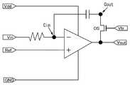
도 1에 도시된 적분 회로(100)는 차동 증폭 회로(101), 저항 소자(102), 용량 소자(103), 및 트랜지스터(104)를 갖는다.The
차동 증폭 회로(101)에는 고전원 전위 Vdd 및 그라운드 전위 GND에 의한 전원 전압이 공급된다. 또한, 그라운드 전위는 저전원 전위 Vss이라도 좋다. 고전원 전위 Vdd가 공급되는 배선의 전위를 고전원 전위 Vdd로부터 그라운드 전위 GND로 전환함으로써 차동 증폭 회로(101)로의 전원 전압의 공급이 정지된다. 또한, 고전원 전위 Vdd가 공급되는 배선의 전위를 그라운드 전위 GND로부터 고전원 전위 Vdd로 전환함으로써 차동 증폭 회로(101)로의 전원 전압의 공급을 재개한다.The
차동 증폭 회로(101)에서의 전원 전압의 공급을 정지 및 재개하는 구성으로 함으로써 전원 전압의 공급을 정지한 기간의 소비 전력을 삭감시킬 수 있다.By setting the structure to stop and resume the supply of the power supply voltage in the
차동 증폭 회로(101)의 비반전 입력 단자는 참조 전압 신호 Ref가 공급되는 단자에 접속되어 있다. 차동 증폭 회로(101)의 반전 입력 단자는 저항 소자(102)를 통하여 입력 신호 Vin이 공급되는 단자에 접속되어 있다. 또한, 차동 증폭 회로(101)의 반전 입력 단자는 용량 소자(103) 및 트랜지스터(104)를 통하여 차동 증폭 회로(101)의 출력 단자에 접속되어 있다. 또한, 차동 증폭 회로(101)의 출력 단자는 출력 신호 Vout를 출력하는 단자에 접속되어 있다.The non-inverting input terminal of the
참조 전압 신호 Ref는 저항 분압 등에 의하여 얻어지는 임의의 정전압의 신호라면 좋다. 일례로서 전원 전압을 2분의 1배로 한 1/2VDD로 하면 좋다.The reference voltage signal Ref may be a signal of any constant voltage obtained by resistance divided voltage or the like. As an example, the power supply voltage may be 1 / 2VDD.
입력 신호 Vin은 방형파나 정현파 등의 신호를 입력하는 구성으로 하면 좋다. 또한, 출력 신호 Vout는 입력 신호 Vin이 적분된 신호를 출력하는 구성으로 하면 좋다.The input signal Vin may be configured to input a signal such as square wave or sine wave. The output signal Vout may be configured to output a signal in which the input signal Vin is integrated.
저항 소자(102)는 단자 중 하나가 입력 신호 Vin이 공급되는 단자에 접속되어 있고, 단자 중 다른 하나가 차동 증폭 회로(101)의 반전 입력 단자에 접속되어 있다.One of the terminals is connected to one terminal of which the input signal Vin is supplied, and the other of the terminals is connected to the inverting input terminal of the
용량 소자(103)는 전극 중 하나가 차동 증폭 회로(101)의 반전 입력 단자에 접속되어 있고, 전극 중 다른 하나가 트랜지스터(104)의 소스 및 드레인 중 하나에 접속되어 있다.In the
또한, 저항 소자(102) 및 용량 소자(103)는 CR 적분 회로를 구성한다. 또한, 도 1의 적분 회로(100)는 트랜지스터(104)를 온 상태(도통 상태)로 함으로써 차동 증폭 회로(101)의 출력 단자와 반전 입력 단자 사이에 용량 소자(103)가 제공된 적분 회로의 회로 구성으로 할 수 있다.In addition, the
또한, 용량 소자(103)는 트랜지스터(104)의 소스 및 드레인 중 하나에 접속되어 있고, 트랜지스터(104)의 소스와 드레인 사이를 흐르는 전류가 용량 소자(103)로 흐르는 구성이 된다. 이 경우에는, 용량 소자와 트랜지스터가 직렬로 접속되어 있다고 할 수 있다.In addition, the
트랜지스터(104)는 게이트가 트랜지스터 제어 신호 Vtr가 공급되는 단자에 접속되어 있고, 소스 및 드레인 중 하나가 용량 소자(103)의 전극 중 다른 하나에 접속되어 있고, 소스 및 드레인 중 다른 하나가 차동 증폭 회로(101)의 출력 단자에 접속되어 있다.The
트랜지스터 제어 신호 Vtr는 전원 전압의 공급의 정지 또는 재개에 따라 트랜지스터(104)를 온 상태 또는 오프 상태(비도통 상태)로 하기 위한 신호를 공급하는 구성으로 하면 좋다.The transistor control signal Vtr may be configured to supply a signal for turning the
또한, 트랜지스터(104)는 채널 폭당의 오프 전류를 반도체층에 실리콘을 갖는 트랜지스터의 오프 전류보다 매우 작은 값인 1×10-22A/μm 이하로 함으로써, 용량 소자(103)의 전극 중 다른 하나와 트랜지스터(104)의 소스 및 드레인 중 하나 사이에 전하를 유지할 수 있다.In addition, the
또한, 오프 전류란 트랜지스터가 오프 상태일 때 소스와 드레인 사이를 흐르는 전류를 말한다. n채널형 트랜지스터(예를 들어 문턱 전압이 0V 내지 2V 정도)에서는 게이트와 소스 사이에 인가되는 전압이 음 전압인 경우에, 소스와 드레인 사이를 흐르는 전류를 말한다.In addition, the off current refers to a current flowing between the source and the drain when the transistor is in the off state. In an n-channel transistor (for example, a threshold voltage of about 0V to 2V), when the voltage applied between the gate and the source is a negative voltage, it refers to a current flowing between the source and the drain.
본 실시형태에서는 트랜지스터의 채널 폭당의 오프 전류를 1×10-22A/μm 이하로 매우 저감시키기 위한 구성으로서 산화물 반도체층에 채널이 형성되는 트랜지스터를 사용하는 것이 적합하다. 또한, 도면에서 트랜지스터(104)는 산화물 반도체층에 채널이 형성되는 트랜지스터인 것을 나타내기 위하여 OS라는 부호를 붙였다.In this embodiment, it is suitable to use a transistor in which a channel is formed in the oxide semiconductor layer as a configuration for greatly reducing the off current per channel width of the transistor to 1 × 10⁻²² A / μm or less. In the figure, the
또한, 상기 구성에서 산화물 반도체 재료 대신에 산화물 반도체 재료와 동등한 오프 전류 특성을 실현할 수 있는 재료를 사용하여도 좋다. 예를 들어 탄소화 실리콘을 비롯한 와이드 갭 재료(보다 구체적으로 말하면 예를 들어 에너지 갭(Eg)이 3eV 보다 큰 반도체 재료) 등을 적용할 수 있다. 또한, 트랜지스터 대신에 MEMS 스위치 등을 사용하여 배선들 사이의 접속을 끊음으로써 전하를 오랜 기간 동안 유지시키는 구성으로 하여도 좋다.In addition, in the above structure, a material capable of realizing off current characteristics equivalent to that of the oxide semiconductor material may be used instead of the oxide semiconductor material. For example, a wide gap material including silicon carbide (more specifically, a semiconductor material having an energy gap Eg greater than 3 eV) may be used. In addition, the structure may be maintained for a long time by disconnecting the wirings using a MEMS switch or the like instead of the transistor.
또한, 도 1의 트랜지스터(104) 외의 차동 증폭 회로(101)를 구성하는 트랜지스터의 반도체층을 트랜지스터(104)의 반도체층과 다르게 할 수 있다. 예를 들어 차동 증폭 회로(101)를 구성하는 트랜지스터는 실리콘층 또는 실리콘 기판에 채널이 형성되는 트랜지스터로 할 수 있다.In addition, the semiconductor layer of the transistors constituting the
여기서, 트랜지스터(104)의 반도체층에 사용되는 산화물 반도체에 대하여 자세히 설명한다.Here, the oxide semiconductor used for the semiconductor layer of the
트랜지스터의 반도체층에 사용되는 산화물 반도체로서는 적어도 인듐(In) 또는 아연(Zn)을 포함하는 것이 바람직하다. 특히, In 및 Zn을 포함하는 것이 바람직하다. 또한, In 및 Zn에 추가하여 산소를 강하게 결합시키는 스테빌라이저를 갖는 것이 바람직하다. 스테빌라이저로서는 갈륨(Ga), 주석(Sn), 지르코늄(Zr), 하프늄(Hf), 및 알루미늄(Al) 중 적어도 어느 것을 가지면 좋다.It is preferable that the oxide semiconductor used for the semiconductor layer of the transistor contains at least indium (In) or zinc (Zn). In particular, it is preferable to include In and Zn. It is also desirable to have a stabilizer that strongly bonds oxygen in addition to In and Zn. The stabilizer may have at least any one of gallium (Ga), tin (Sn), zirconium (Zr), hafnium (Hf), and aluminum (Al).
또한, 다른 스테빌라이저로서 란타노이드(lanthanoid)인 란탄(La), 세륨(Ce), 프라세오디뮴(Pr), 네오디뮴(Nd), 사마륨(Sm), 유로퓸(Eu), 가돌리늄(Gd), 테르븀(Tb), 디스프로슘(Dy), 홀뮴(Ho), 에르븀(Er), 툴륨(Tm), 이테르븀(Yb), 루테튬(Lu) 중 임의의 1종류 또는 복수 종류를 가져도 좋다.In addition, as other stabilizers, lanthanoids such as lanthanum (La), cerium (Ce), praseodymium (Pr), neodymium (Nd), samarium (Sm), europium (Eu), gadolinium (Gd), and terbium (Tb) ), Dysprosium (Dy), holmium (Ho), erbium (Er), thulium (Tm), ytterbium (Yb) and lutetium (Lu).
예를 들어, 4원계 금속의 산화물인 In-Sn-Ga-Zn계 산화물이나, 3원계 금속의 산화물인 In-Ga-Zn계 산화물, In-Sn-Zn계 산화물, In-Zr-Zn계 산화물, In-Al-Zn계 산화물, Sn-Ga-Zn계 산화물, Al-Ga-Zn계 산화물, Sn-Al-Zn계 산화물, In-Hf-Zn계 산화물, In-La-Zn계 산화물, In-Ce-Zn계 산화물, In-Pr-Zn계 산화물, In-Nd-Zn계 산화물, In-Sm-Zn계 산화물, In-Eu-Zn계 산화물, In-Gd-Zn계 산화물, In-Tb-Zn계 산화물, In-Dy-Zn계 산화물, In-Ho-Zn계 산화물, In-Er-Zn계 산화물, In-Tm-Zn계 산화물, In-Yb-Zn계 산화물, In-Lu-Zn계 산화물이나, 2원계 금속의 산화물인, In-Zn계 산화물, Sn-Zn계 산화물, Al-Zn계 산화물, Zn-Mg계 산화물, Sn-Mg계 산화물, In-Mg계 산화물, In-Ga계 산화물이나, 1원계 금속의 산화물인 In계 산화물, Sn계 산화물, Zn계 산화물 등을 사용할 수 있다.For example, In-Sn-Ga-Zn-based oxides which are oxides of quaternary metals, In-Ga-Zn-based oxides, In-Sn-Zn-based oxides, and In-Zr-Zn-based oxides which are oxides of ternary metals. , In-Al-Zn oxide, Sn-Ga-Zn oxide, Al-Ga-Zn oxide, Sn-Al-Zn oxide, In-Hf-Zn oxide, In-La-Zn oxide, In -Ce-Zn oxide, In-Pr-Zn oxide, In-Nd-Zn oxide, In-Sm-Zn oxide, In-Eu-Zn oxide, In-Gd-Zn oxide, In-Tb -Zn oxide, In-Dy-Zn oxide, In-Ho-Zn oxide, In-Er-Zn oxide, In-Tm-Zn oxide, In-Yb-Zn oxide, In-Lu-Zn In-Zn oxides, Sn-Zn oxides, Al-Zn oxides, Zn-Mg oxides, Sn-Mg oxides, In-Mg oxides, and In-Ga which are oxides of oxides or binary metals In-type oxides, Sn-based oxides, Zn-based oxides, and the like, which are oxides of oxides or primary metals, can be used.
또한, 여기서 예를 들어 In-Ga-Zn계 산화물이란 In, Ga 및 Zn을 주성분으로 포함한 산화물이라는 뜻이며, In과 Ga 및 Zn의 비율은 불문한다.Here, for example, an In—Ga—Zn-based oxide means an oxide containing In, Ga, and Zn as main components, and the ratio of In, Ga, and Zn is irrelevant.
또한, 산화물 반도체로서 InMO3(ZnO)m(m>0)으로 표기되는 재료를 사용하여도 좋다. 또한, M은 Ga, Fe, Mn, 및 Co 중에서 선택된 하나의 금속 원소 또는 복수의 금속 원소를 나타낸다. 또한, 산화물 반도체로서 In2SnO5(ZnO)n(n>0)로 표기되는 재료를 사용하여도 좋다.As the oxide semiconductor, a material represented by InMO3 (ZnO)m (m> 0) may be used. In addition, M represents one metal element or a plurality of metal elements selected from Ga, Fe, Mn, and Co. As the oxide semiconductor, a material represented by In2 SnO5 (ZnO)n (n> 0) may be used.
예를 들어, 원자수비가 In:Ga:Zn=3:1:2, In:Ga:Zn=1:1:1, 또는 In:Ga:Zn=2:2:1인 In-Ga-Zn계 산화물이나 그 조성의 근방의 조성을 갖는 산화물을 사용할 수 있다. 또는, 원자수비가 In:Sn:Zn=1:1:1, In:Sn:Zn=2:1:3, 또는 In:Sn:Zn=2:1:5인 In-Sn-Zn계 산화물이나 그 조성의 근방의 조성을 갖는 산화물을 사용하면 좋다.For example, an In-Ga-Zn system having an atomic ratio of In: Ga: Zn = 3: 1: 2, In: Ga: Zn = 1: 1: 1, or In: Ga: Zn = 2: 2: 1 Oxides and oxides having a composition near the composition can be used. Or an In—Sn—Zn oxide having an atomic ratio of In: Sn: Zn = 1: 1: 1, In: Sn: Zn = 2: 1: 3, or In: Sn: Zn = 2: 1: 5 An oxide having a composition in the vicinity of the composition may be used.
또한, 예를 들어 In, Ga, 및 Zn의 원자수비가 In:Ga:Zn=a:b:c(a+b+c=1)인 산화물의 조성이 원자수비가 In:Ga:Zn=A:B:C(A+B+C=1)인 산화물의 조성의 근방이라는 것은 a, b, 및 c가 수학식 1을 만족하는 것을 가리킨다.For example, the composition of the oxide whose atomic ratio of In, Ga, and Zn is In: Ga: Zn = a: b: c (a + b + c = 1) has an atomic ratio of In: Ga: Zn = A The vicinity of the composition of the oxide of: B: C (A + B + C = 1) indicates that a, b, and c satisfy the expression (1).

r은 예를 들어 0.05로 하면 좋다. 다른 산화물에서도 마찬가지다.r may be 0.05, for example. The same is true for other oxides.
그러나, 이들에 한정되지 않고, 필요한 반도체 특성(전계 효과 이동도, 문턱 전압 등)에 따라 적절한 조성을 갖는 것을 사용하면 좋다. 또한, 필요한 반도체 특성을 얻기 위하여 캐리어 농도나 불순물 농도, 결함 밀도, 금속 원소와 산소의 원자수비, 원자간 거리, 및 밀도 등을 적절하게 하는 것이 바람직하다.However, the present invention is not limited to these, and those having an appropriate composition may be used in accordance with required semiconductor characteristics (field effect mobility, threshold voltage, etc.). In addition, in order to obtain necessary semiconductor characteristics, it is preferable to appropriately set the carrier concentration, the impurity concentration, the defect density, the atomic ratio of the metal element and oxygen, the interatomic distance, the density, and the like.
또한, 산화물 반도체가 반도체층에 사용된 트랜지스터는 산화물 반도체를 고순도화함으로써, 오프 전류(여기서는 오프 상태일 때 예를 들어 소스 전위를 기준으로 한 경우의 게이트 전위와의 전위차가 문턱 전압 이하인 경우의 드레인 전류로 함)를 충분히 낮게 할 수 있다. 예를 들어, 가열 성막에 의하여 수소나 수산기를 산화물 반도체 내에 포함시키지 않도록 하고, 또는 성막 후의 가열에 의하여 막 내에서 제거하여 고순도화를 도모할 수 있다.In addition, the transistor in which the oxide semiconductor is used for the semiconductor layer makes the oxide semiconductor highly purified, so that the drain current when the potential difference with the off current (here, the gate potential when the source potential is referenced, for example, in the off state is below the threshold voltage). Current) can be sufficiently low. For example, it is possible to prevent hydrogen and hydroxyl groups from being included in the oxide semiconductor by heating film formation or to remove the film from the film by heating after film formation to achieve high purity.
또한, 산화물 반도체를 고순도화시켜 극소의 오프 전류를 검출하기 위하여 비교적 사이즈가 큰 트랜지스터를 제작하고, 오프 전류를 측정함으로써 실제로 흐르는 오프 전류를 어림잡을 수 있다. 도 2는 사이즈가 큰 트랜지스터로서 채널 폭 W를 1m(1000000μm), 채널 길이 L을 3μm로 한 경우에 온도를 150℃, 125℃, 85℃, 27℃로 변화시킨 경우의 채널 폭 W 1μm당의 오프 전류를 아레니우스 플롯으로 나타낸 도면을 도시한 것이다. 도 2에서 알 수 있는 바와 같이, 27℃에서의 오프 전류는 3×10-26A/μm로 매우 작은 것을 알 수 있다. 또한, 온도를 상승시켜 오프 전류를 측정한 것은 실온에서는 전류가 매우 작아 측정하기 어려웠기 때문이다.In addition, by fabricating a transistor of relatively large size in order to increase the purity of the oxide semiconductor to detect the minimum off current, the off current can be estimated by measuring the off current. Fig. 2 shows a transistor having a large size, the channel width W being 1 m (1000000 µm) and the channel length L being 3 µm, when the temperature is changed to 150 ° C, 125 ° C, 85 ° C and 27 ° C. The figure shows the current as an Areneus plot. As can be seen in FIG. 2, it can be seen that the off current at 27 ° C. is very small, 3 × 10⁻²⁶ A / μm. In addition, the off current was measured by raising the temperature because the current was very small and difficult to measure at room temperature.
고순도화된 In-Ga-Zn계 산화물이 채널 형성 영역에 사용된 트랜지스터에서 채널 길이가 10μm, 반도체막의 막 두께가 30nm, 드레인 전압이 1V 내지 10V 정도의 범위인 경우에, 오프 전류를 1×10-13A 이하로 할 수 있다. 또한, 채널 폭당의 오프 전류(오프 전류를 트랜지스터의 채널 폭으로 나눈 값)는 1×10-23A/μm(10yA/μm) 내지 1×10-22A/μm(100yA/μm) 정도로 할 수 있다.In the transistor in which the highly purified In-Ga-Zn oxide is used in the channel formation region, the off current is 1 × 10 when the channel length is 10 μm, the film thickness of the semiconductor film is 30 nm, and the drain voltage is about 1V to 10V. It can be-13 A or less. Further, the off current per channel width (the off current divided by the channel width of the transistor) can be about 1 × 10-23 A / μm (10yA / μm) to 1 × 10-22 A / μm (100yA / μm). have.
여기까지 트랜지스터(104)의 반도체층에 사용되는 산화물 반도체에 대하여 설명하였다.The oxide semiconductor used for the semiconductor layer of the
트랜지스터의 채널 폭당의 오프 전류가 반도체층에 실리콘을 갖는 트랜지스터의 오프 전류보다 매우 작은 값인 1×10-22A/μm 이하인 트랜지스터(104)는 트랜지스터(104)가 온 상태라면 도 3a에 도시된 회로 구성과 같이 적분 회로의 회로 구성이 된다. 구체적으로 말하면, 트랜지스터(104)가 온 상태가 됨으로써 용량 소자(103)의 전극 중 다른 하나와 차동 증폭 회로(101)의 출력 단자가 전기적으로 접속된 상태(도 3a의 파선(104_ON))로 할 수 있다. 또한, 트랜지스터(104)가 오프 상태가 됨으로써 용량 소자(103)의 전극 중 다른 하나와 차동 증폭 회로(101)의 출력 단자가 전기적으로 접속되지 않은 상태(도 3b의 파선(104_OFF))로 할 수 있다.The
또한, 도 3b와 같이, 용량 소자(103)의 전극 중 다른 하나와 차동 증폭 회로(101)의 출력 단자가 전기적으로 접속되지 않은 상태로 함으로써 용량 소자(103)의 양단의 전극에 전하가 유지되는 상태를 실현할 수 있다. 용량 소자(103)의 양단의 전극에 유지되는 전하에 의한 전압 Vc는 적분 회로에서의 적분값에 상당한다. 트랜지스터(104)의 오프 전류는 매우 작기 때문에 전원 전압의 공급을 정지하더라도 상기 적분값을 일정 기간 동안 유지할 수 있다.In addition, as shown in FIG. 3B, when the other of the electrodes of the
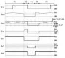
다음에, 도 1에 도시된 적분 회로(100)의 통상시의 동작 및 전원 전압의 공급을 정지 및 재개할 때의 동작에 대하여 설명한다. 도 4에는 동작을 설명하기 위하여 도 1에 도시된 적분 회로(100)의 노드에 부호를 붙인 도면을 도시하였다. 도 4에 도시된 도면에서는 용량 소자(103)의 전극 중 하나에 전기적으로 접속된 노드를 노드 Cin으로 하고, 용량 소자(103)의 전극 중 다른 하나에 전기적으로 접속된 노드를 노드 Cout로 하여 설명한다.Next, the normal operation of the integrating
또한, 도 4와 함께 도 5에서는 입력 신호 Vin, 출력 신호 Vout, 노드 Cout의 전위, 노드 Cin의 전위, 트랜지스터 제어 신호 Vtr, 참조 전압 신호 Ref, 및 고전원 전위 Vdd가 공급되는 배선의 전위의 변화를 나타내는 타이밍 차트를 나타낸다. 도 5에 도시된 타이밍 차트에서는 통상 동작 기간을 기간(T1), 전원 공급 정지 준비 기간을 기간(T2), 전원 공급 정지 기간을 기간(T3), 전원 공급 재개 준비 기간을 기간(T4)으로 나누어 설명한다.4 and 5, the input signal Vin, the output signal Vout, the potential of the node Cout, the potential of the node Cin, the transistor control signal Vtr, the reference voltage signal Ref, and the potential of the wiring to which the high power supply potential Vdd is supplied. Shows a timing chart. In the timing chart shown in Fig. 5, the normal operation period is divided into the period T1, the power supply stop preparation period by the period T2, the power supply stop period by the period T3, and the power supply resumption preparation period by the period T4. Explain.
또한, 도 4 및 도 5의 적분 회로의 동작은 트랜지스터의 도전형이 n채널형인 것으로 가정하여 설명한다. 또한, 각 신호가 고전원 전위 Vdd와 그라운드 전위 GND의 2값 사이의 전위를 갖는 것으로 하여 설명한다. 또한, 고전원 전위 Vdd에 의거한 신호를 H 신호라고 하고, 그라운드 전위 GND에 의거한 신호를 L 신호라고 하는 경우도 있다. 또한, 전원 전압의 공급을 정지할 때는 고전원 전위 Vdd를 그라운드 전위 GND로 하여 전원 전압의 공급을 정지하는 것으로 가정하여 설명한다.In addition, the operation of the integrating circuit of FIGS. 4 and 5 will be described assuming that the conductivity type of the transistor is n-channel type. In addition, it is assumed that each signal has a potential between two values of the high power source potential Vdd and the ground potential GND. In addition, a signal based on the high power source potential Vdd may be referred to as an H signal, and a signal based on the ground potential GND may be referred to as an L signal. In addition, it is assumed that the supply of the power supply voltage is stopped with the high power supply potential Vdd being the ground potential GND.
도 5의 기간(T1)의 동작에 대하여 설명한다.The operation of the period T1 in FIG. 5 will be described.
기간(T1)에 적분 회로(100)는 입력 신호 Vin의 H 신호 또는 L 신호를 적분한 파형의 출력 신호 Vout를 출력한다. 구체적으로 말하면, 입력 신호 Vin의 H 신호 또는 L 신호에 따라 전위의 상승 또는 하강을 반복하는 3각파를 출력 신호 Vout로서 출력한다.In the period T1, the integrating
또한, 기간(T1)에 참조 전압 신호 Ref의 전위는 참조 전압 Vref가 된다. 고전원 전위 Vdd가 공급되는 배선의 전위는 고전원 전위 Vdd가 된다. 또한, 트랜지스터 제어 신호 Vtr는 H 신호가 되므로 트랜지스터(104)는 온 상태가 된다.In the period T1, the potential of the reference voltage signal Ref becomes the reference voltage Vref. The potential of the wiring to which the high power supply potential Vdd is supplied becomes the high power supply potential Vdd. In addition, since the transistor control signal Vtr becomes the H signal, the
또한, 기간(T1)에 출력 신호 Vout의 변동에 따라 노드 Cout의 전위도 변동된다. 노드 Cin의 전위는 참조 전압 신호 Ref와 가상 단락되기 때문에 전위 Vref가 된다.Further, in the period T1, the potential of the node Cout also changes in accordance with the change of the output signal Vout. The potential of the node Cin becomes the potential Vref because it is virtually shorted with the reference voltage signal Ref.
다음에, 도 5의 기간(T2)의 동작에 대하여 설명한다.Next, the operation of the period T2 in FIG. 5 will be described.
기간(T2)에 적분 회로(100)는 전원 전압의 공급을 정지하기 전에, 적분값에 대응하는 용량 소자(103)의 양단의 전극의 전압을 유지하기 위한 동작을 실시한다.In the period T2, before the supply of the power supply voltage is stopped, the integrating
기간(T2)에 적분 회로(100)는 입력 신호 Vin을 적분한 파형이 출력 신호 Vout로서 출력하는 동작을 정지한다. 구체적으로 말하면, 도 5에 도시된 바와 같이, 입력 신호 Vin을 기간(T1)의 입력 신호 Vin의 전위인 고전원 전위 Vdd로 고정한다. 기간(T2)에는 음의 피드백이 없으므로 차동 증폭 회로(101)는 단순히 차동 증폭을 실시하는 회로가 된다. 그러므로, 출력 신호 Vout는 도 5의 예에서는 그라운드 전위 GND가 된다. 또한, 기간(T2)의 파형은 도 5에 도시된 예와 반대로 입력 신호 Vin이 그라운드 전위 GND로 고정되어 출력 신호 Vout가 고전원 전위 Vdd가 되어도 좋다.In the period T2, the integrating
또한, 기간(T2)에 참조 전압 신호 Ref의 전위는 참조 전압 Vref가 된다. 고전원 전위 Vdd가 공급되는 배선의 전위는 고전원 전위 Vdd가 된다. 또한, 트랜지스터 제어 신호 Vtr는 L 신호가 되므로 트랜지스터(104)는 오프 상태가 된다.In the period T2, the potential of the reference voltage signal Ref becomes the reference voltage Vref. The potential of the wiring to which the high power supply potential Vdd is supplied becomes the high power supply potential Vdd. In addition, since the transistor control signal Vtr becomes the L signal, the
또한, 기간(T2)에 트랜지스터(104)가 오프 상태가 된다. 본 실시형태의 적분 회로의 구성에서는 오프 전류가 작은 트랜지스터(104)를 사용한다. 그러므로, 전하의 방전을 억제할 수 있고, 용량 소자(103)의 양단의 전극에 유지되는 전압(Vckp-Vref)을 유지할 수 있다.In addition, the
또한, Vckp는 기간(T1)과 같이 노드 Cin에 참조 전압 Vref가 공급될 때 트랜지스터(104)를 오프 상태로 하기 직전의 노드 Cout의 전위다. 즉 트랜지스터(104)를 오프 상태로 함으로써, 노드 Cin과 노드 Cout 사이의 용량 소자(103)에 유지되는 전압은 노드 Cout의 전위 Vckp와 참조 전압의 전위 Vref의 차이다(Vckp-Vref).In addition, Vckp is a potential of the node Cout immediately before the
기간(T2)에 노드 Cin의 전위는 전하의 방전에 의하여 입력 신호 Vin과 등전위가 된다. 따라서, 도 5에 도시된 바와 같이, 전위 Vref로부터 고전원 전위 Vdd로 변동된다.In the period T2, the potential of the node Cin becomes equipotential to the input signal Vin by discharge of charge. Thus, as shown in FIG. 5, the potential is varied from the potential Vref to the high power potential Vdd.
또한, 노드 Cout의 전위는 전하의 방전은 없지만 용량 소자(103)의 용량 결합에 의한 노드 Cin의 전위의 변동에 따라 변동된다. 구체적으로 말하면, 일례로서 도시된 도 5에서는 노드 Cout의 전위가 Vckp로부터 (Vckp-Vref+Vdd)로 변동된다.In addition, although the potential of the node Cout does not discharge electric charges, the potential of the node Cout varies depending on the change in the potential of the node Cin due to the capacitive coupling of the
또한, 기간(T2)의 용량 소자(103)의 양단의 전극에 인가되는 전압인 (Vckp-Vref)는 용량 소자(103)의 양단의 전극에 유지되는 적분값에 상당한다.In addition, Vckp-Vref, which is the voltage applied to the electrodes at both ends of the
다음에, 도 5의 기간(T3)의 동작에 대하여 설명한다.Next, the operation of the period T3 in FIG. 5 will be described.
기간(T3)에 적분 회로(100)는 전원 전압의 공급을 정지한다.In the period T3, the integrating
기간(T3)에 적분 회로(100)는 전원 전압의 공급이 정지되므로 입력 신호 Vin 및 출력 신호 Vout가 함께 그라운드 전위 GND가 된다.In the period T3, since the supply of the power supply voltage is stopped in the
또한, 기간(T3)에 참조 전압 신호 Ref의 전위는 전원 전압의 공급이 정지됨과 동시에 그라운드 전위 GND가 된다. 고전원 전위 Vdd가 공급되는 배선의 전위는 그라운드 전위 GND가 된다. 또한, 트랜지스터 제어 신호 Vtr는 L 신호가 되므로 트랜지스터(104)는 오프 상태가 된다.In the period T3, the potential of the reference voltage signal Ref becomes ground potential GND while the supply of the power supply voltage is stopped. The potential of the wiring to which the high power supply potential Vdd is supplied becomes the ground potential GND. In addition, since the transistor control signal Vtr becomes the L signal, the
또한, 기간(T3)에 트랜지스터(104)가 오프 상태가 된다. 본 실시형태의 적분 회로의 구성에서는 오프 전류가 작은 트랜지스터(104)를 사용한다. 그러므로, 전하의 방전을 억제할 수 있고, 용량 소자(103)의 양단의 전극에 유지되는 전압(Vckp-Vref)을 유지할 수 있다.In addition, the
또한, 기간(T3)의 노드 Cin의 전위는 전원 전압의 공급이 정지됨과 동시에 그라운드 전위 GND로 저하된다. 그러므로, 노드 Cout의 전위는 용량 결합에 의하여 (Vckp-Vref)로 저하된 상태로 유지된다.In addition, the potential of the node Cin in the period T3 is lowered to the ground potential GND while the supply of the power supply voltage is stopped. Therefore, the potential of the node Cout remains lowered to (Vckp-Vref) by capacitive coupling.
다음에, 도 5의 기간(T4)의 동작에 대하여 설명한다.Next, the operation of the period T4 of FIG. 5 will be described.
기간(T4)에 적분 회로(100)로의 전원 전압의 공급을 재개하고, 적분 회로(100)는 입력 신호 Vin을 입력하기 전에 각 전위를 통상 동작시의 전위로 되돌리기 위한 동작을 실시한다.In the period T4, the supply of the power supply voltage to the integrating
기간(T4)에 적분 회로(100)로의 전원 전압의 공급을 재개하고, 적분 회로(100)는 입력 신호 Vin의 변동에 따른 출력 신호 Vout를 출력한다. 구체적으로 말하면, 도 5에 도시된 바와 같이, 입력 신호 Vin을 그라운드 전위 GND로 고정한다. 기간(T4)에는 음의 피드백이 없으므로 차동 증폭 회로(101)는 단순히 차동 증폭을 실시하는 회로가 된다. 그러므로, 출력 신호 Vout는 도 5의 예에서는 고전원 전위 Vdd가 된다. 또한, 기간(T4)의 파형은 도 5에 도시된 예와 반대로 입력 신호 Vin이 고전원 전위 Vdd로 고정되어 출력 신호 Vout가 그라운드 전위 GND가 되어도 좋다.In the period T4, the supply of the power supply voltage to the integrating
또한, 기간(T4)에 참조 전압 신호 Ref의 전위는 참조 전압 Vref가 된다. 고전원 전위 Vdd가 공급되는 배선의 전위는 고전원 전위 Vdd가 된다. 또한, 트랜지스터 제어 신호 Vtr는 L 신호가 되므로 트랜지스터(104)는 오프 상태가 된다.In the period T4, the potential of the reference voltage signal Ref becomes the reference voltage Vref. The potential of the wiring to which the high power supply potential Vdd is supplied becomes the high power supply potential Vdd. In addition, since the transistor control signal Vtr becomes the L signal, the
또한, 기간(T4)에 트랜지스터(104)가 오프 상태가 된다. 본 실시형태의 적분 회로의 구성에서는 오프 전류가 작은 트랜지스터(104)를 사용한다. 그러므로, 전하의 방전을 억제할 수 있고, 용량 소자(103)의 양단의 전극에 유지되는 전압(Vckp-Vref)을 유지할 수 있다.In the period T4, the
또한, 기간(T4)의 노드 Cin의 전위는 입력 신호 Vin과 등전위가 된다. 따라서, 노드 Cin의 전위는 도 5에 도시된 바와 같이 그라운드 전위 GND를 유지한다. 또한, 노드 Cout의 전위는 기간(T3)의 (Vckp-Vref)를 유지한다.In addition, the potential of the node Cin in the period T4 becomes equal to the input signal Vin. Therefore, the potential of the node Cin maintains the ground potential GND as shown in FIG. In addition, the potential of the node Cout maintains (Vckp-Vref) of the period T3.
도 5의 기간(T4) 후, 다시 통상 동작에 상당하는 기간(T1)으로 돌아간다. 이 때, 트랜지스터(104)를 온 상태로 한다. 본 실시형태의 적분 회로의 구성에서는 오프 전류가 작은 트랜지스터(104)를 사용한다. 그러므로, 전하의 방전이 억제되므로 다시 실시되는 용량 소자(103)로의 충전을 고속화시킬 수 있다. 그리고, 용량 소자(103)로의 전하의 충전에 걸리는 시간을 짧게 할 수 있다. 그리고, 적분 회로(100)는 입력 신호 Vin의 H 신호 또는 L 신호를 적분한 파형의 출력 신호 Vout를 출력할 수 있다.After the period T4 of FIG. 5, the flow returns to the period T1 corresponding to normal operation again. At this time, the
여기까지 도 1에 도시된 적분 회로(100)의 동작을 설명하였다.The operation of the integrating
상술한 바와 같이, 본 실시형태의 적분 회로의 구성에서는 오프 전류가 작은 트랜지스터를 사용하여 전원 전압의 공급을 정지할 때의 전하의 방전을 억제하고, 전원 전압의 공급을 재개할 때의 용량 소자로의 전하의 충전을 고속으로 실시할 수 있다. 따라서, 본 발명의 일 형태에서는 전원 전압의 공급을 정지 및 재개할 때 용량 소자로부터 전하가 방전되는 것을 저감하고, 충전에 걸리는 시간을 짧게 할 수 있다.As described above, in the configuration of the integrating circuit of the present embodiment, it is possible to suppress the discharge of the electric charges when the supply of the power supply voltage is stopped by using a transistor with a small off-current, and to use the capacitor as a capacitor when the supply of the supply voltage is resumed. Can be charged at a high speed. Therefore, in one embodiment of the present invention, when the supply of the power supply voltage is stopped and resumed, discharge of charge from the capacitor can be reduced, and the time required for charging can be shortened.
본 실시형태는 다른 실시형태와 적절히 조합하여 실시할 수 있다.The present embodiment can be implemented in appropriate combination with other embodiments.
(실시형태 2)(Embodiment 2)
본 실시형태에서는 상기 실시형태 1에서 설명한 적분 회로(100)의 변형예에 대하여 설명한다.In this embodiment, a modification of the integrating
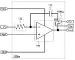
도 6에 도시된 적분 회로(100rp)는 차동 증폭 회로(101), 저항 소자(102), 용량 소자(103), 및 트랜지스터(104rp)를 갖는다.The integrating circuit 100rp shown in FIG. 6 has a
트랜지스터(104rp)는 실시형태 1의 도 1의 트랜지스터(104)의 위치를 용량 소자(103)의 전극 중 다른 하나 측으로부터 용량 소자(103)의 전극 중 하나 측으로 바꾼 구성을 갖는다. 트랜지스터(104rp)의 위치를 차동 증폭 회로(101)의 출력 단자 측으로부터 반전 입력 단자 측으로 바꿈으로써 출력 단자 측에서의 트랜지스터로 인한 기생 용량의 저감을 도모할 수 있다.The transistor 104rp has a configuration in which the position of the
또한, 도 10a에 도시된 적분 회로(100rA)는 차동 증폭 회로(101), 저항 소자(102), 용량 소자(103), 트랜지스터(104), 및 저항 소자(105A)를 갖는다.In addition, the integrating circuit 100rA shown in FIG. 10A includes a
저항 소자(105A)는 실시형태 1의 도 1의 용량 소자(103) 및 트랜지스터(104)에 전기적으로 병렬로 제공된 구성을 갖는다. 저항 소자(105A)를 용량 소자(103) 및 트랜지스터(104)에 전기적으로 병렬로 제공함으로써 용량 소자(103)에서의 전하의 포화를 억제할 수 있다.The
도 10b에 도시된 적분 회로(100rB)는 차동 증폭 회로(101), 저항 소자(102), 용량 소자(103), 트랜지스터(104), 트랜지스터(104r), 및 저항 소자(105B)를 갖는다.The integrating circuit 100rB shown in FIG. 10B has a
트랜지스터(104r) 및 저항 소자(105B)가 실시형태 1의 도 1의 용량 소자(103)에 전기적으로 병렬로 제공된 구성이다. 트랜지스터(104r) 및 저항 소자(105B)를 용량 소자(103)에 전기적으로 병렬로 제공함으로써 트랜지스터(104r) 및 트랜지스터(104)의 양쪽 모두를 오프 상태로 하였을 때 적분값을 유지할 수 있음과 함께 트랜지스터(104r) 및 트랜지스터(104)의 양쪽 모두를 온 상태로 하였을 때 용량 소자(103)에서의 전하의 포화를 억제할 수 있다.The
본 실시형태는 다른 실시형태와 적절히 조합하여 실시할 수 있다.The present embodiment can be implemented in appropriate combination with other embodiments.
(실시형태 3)(Embodiment 3)
본 실시형태에서는 상기 실시형태 1에서 설명한 적분 회로(100)의 변형예에 대하여 설명한다.In this embodiment, a modification of the integrating
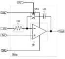
도 7에 도시된 적분 회로(100bg)는 차동 증폭 회로(101), 저항 소자(102), 용량 소자(103), 및 트랜지스터(104bg)를 갖는다.The integrating circuit 100bg shown in FIG. 7 has a
트랜지스터(104bg)는 실시형태 1의 도 1의 트랜지스터(104)를 백 게이트가 제공된 트랜지스터(104bg)로 한 것이고, 상기 트랜지스터(104bg)의 백 게이트에 문턱 전압을 제어하기 위한 백 게이트 전압 Vbg가 입력되는 구성이다.The transistor 104bg is a transistor 104bg provided with a back gate of the
백 게이트 전압 Vbg의 전위를 제어하여 트랜지스터(104bg)의 문턱 전압을 제어하는 구성으로 함으로써 도 7의 적분 회로(100bg)는 용량 소자(103)에서의 전하 유지 동작 등을 더 확실히 실시할 수 있다.By configuring the threshold voltage of the transistor 104bg by controlling the potential of the back gate voltage Vbg, the integrating circuit 100bg of FIG. 7 can more reliably perform the charge holding operation in the
도 11에 도시된 적분 회로(100W)는 차동 증폭 회로(101), 차동 증폭 회로(101W), 저항 소자(102), 용량 소자(103), 및 트랜지스터(104)를 갖는다.The integrating
도 11에 도시된 바와 같이, 차동 증폭 회로(101W)를 차동 증폭 회로(101)에 직렬로 접속시킨 2단 차동 증폭 회로로 할 수도 있다. 상기 구성으로 함으로써 차동 증폭 회로(101)에서의 노이즈의 영향이 저감된 적분 회로로 할 수 있다.As shown in Fig. 11, the
본 실시형태는 상기 실시형태와 적절히 조합하여 실시할 수 있다.The present embodiment can be implemented in appropriate combination with the above embodiment.
(실시형태 4)(Fourth Embodiment)
본 실시형태에서는 상기 실시형태 1 내지 실시형태 3에서 설명한 적분 회로를 위상 동기 회로(아래에서는 PLL 회로라고 함)가 갖는 액티브 루프 필터에 제공한 형태에 대하여 설명한다.In this embodiment, an embodiment in which the integrating circuits described in the first to third embodiments are provided to an active loop filter included in a phase locked circuit (hereinafter referred to as a PLL circuit) will be described.
도 8에 도시된 PLL 회로(200)는 위상 비교기(201), 액티브 루프 필터(202), 전압 제어 발진기(203)(VCO(Voltage Controlled Oscillator)라고도 함), 및 분주기(204)를 갖는다.The
상기 실시형태에서 설명한 적분 회로를 액티브 루프 필터(202)에 사용함으로써 전원 전압의 공급을 정지할 때의 전하의 방전을 억제하고, 전원 전압의 공급을 재개할 때의 용량 소자로의 전하의 충전을 고속으로 실시할 수 있다. 그러므로, 본 발명의 일 형태에서는 PLL 회로로의 전원 전압의 공급을 정지 및 재개하는 경우에 용량 소자로부터의 전하의 방전을 저감시켜 충전에 걸리는 시간을 짧게 할 수 있다.By using the integrating circuit described in the above embodiment for the
본 실시형태는 상기 실시형태와 적절히 조합하여 실시할 수 있다.The present embodiment can be implemented in appropriate combination with the above embodiment.
(실시형태 5)(Embodiment 5)
본 실시형태에서는 상기 실시형태 1 내지 실시형태 3에서 설명한 차동 증폭 회로를 구성하는 트랜지스터와, 용량 소자에 전기적으로 직렬로 접속된 트랜지스터가 적층되도록 제공된 반도체 장치의 구성에 대하여 도 9의 단면도를 참조하여 설명한다.In this embodiment, referring to the cross-sectional view of FIG. 9 for the configuration of the transistors constituting the differential amplifier circuits described in
또한, 도 9에 도시된 반도체 장치의 단면도에서는 하층부를 구성하는 차동 증폭 회로를 구성하는 트랜지스터의 일례로서 n채널형 트랜지스터(331) 및 p채널형 트랜지스터(332)를 도시하였고, 상층부를 구성하는 트랜지스터로서 산화물 반도체층에 채널이 형성되는 트랜지스터(300) 및 용량 소자(301)를 도시하였다.In the cross-sectional view of the semiconductor device shown in FIG. 9, an n-
도 9에 도시된 반도체 장치는 하부 소자층(321)에 실리콘 재료가 채널 영역에 사용된 n채널형 트랜지스터(331) 및 p채널형 트랜지스터(332)를 갖고, 배선층(322) 및 배선층(323)을 개재(介在)하여 하부 소자층(321)과 전기적으로 접속된 상부 소자층(324)에 도 7에 도시된 트랜지스터(104bg) 및 용량 소자(103)를 갖는다.The semiconductor device shown in FIG. 9 has an n-
도 9의 n채널형 트랜지스터(331)는 반도체 재료(예를 들어, 실리콘 등)를 포함한 기판(333) 위에 BOX(Buried Oxide)층(334)을 개재하여 제공된 SOI층(335)과, SOI층(335)에 형성된 n형 불순물 영역(336)과, 게이트 절연막(337)과, 게이트 전극(338)을 갖는다. SOI층(335)에는 n형 불순물 영역(336) 이외에 금속간 화합물 영역 및 채널 형성 영역(이들은 도시되지 않았음)이 제공되어 있다. 또한, p채널형 트랜지스터(332)는 SOI층(335) 내에 p형 불순물 영역(339)이 형성되어 있다.The n-
n채널형 트랜지스터(331) 및 p채널형 트랜지스터(332)가 각각 갖는 SOI층(335)들 사이에 소자 분리 절연층(342)이 제공되어 있고, n채널형 트랜지스터(331) 및 p채널형 트랜지스터(332)를 덮도록 절연막(340)이 제공되어 있다. 또한, n채널형 트랜지스터(331) 및 p채널형 트랜지스터(332)에는 도 9에 도시된 바와 같이 게이트 전극(338)의 측면에 측벽이 제공되어 있고, 불순물 농도가 다른 영역을 포함한 n형 불순물 영역(336) 및 p형 불순물 영역(339)으로 하여도 좋다.An
n형 불순물 영역(336) 및 p형 불순물 영역(339) 위의 절연막(340)은 개구부를 갖고, 개구부를 메우도록 배선(341)이 제공되어 있다. 절연막(340) 및 배선(341) 위의 배선층(322)에서는 절연막(344)에 개구부를 갖고, 개구부를 메우도록 배선(351) 및 배선(352)이 제공되어 있다. 절연막(344), 배선(351), 및 배선(352) 위의 배선층(323)에서는 절연막(345)에 개구부를 갖고, 개구부를 메우도록 배선(353)이 제공되어 있다.The insulating
또한, 하부 소자층(321)의 배선(341), 배선층(322)의 배선(351) 및 배선(352), 및 배선층(323)의 배선(353)은 듀얼 다마신법(dual damascene method)을 사용하여 형성하면 좋다. 또한, 콘택트 플러그를 형성하여 다른 배선층들 사이를 접속시켜도 좋다.In addition, the
반도체 재료를 구비한 SOI층(335)을 사용한 n채널형 트랜지스터(331) 및 p채널형 트랜지스터(332)는 트랜지스터(300)보다 고속 동작 및 미세화가 가능하다.The n-
배선층(323)의 상면은 CMP(Chemical Mechanical Polishing) 처리하여 배선(353)의 상면을 노출시킨 후에 트랜지스터(300) 및 용량 소자(301)를 형성하면 좋다.The upper surface of the
트랜지스터(300)는 절연막(345) 및 배선(353) 위에 산화물 반도체막(401), 소스 전극(402A), 드레인 전극(402B), 게이트 절연막(403), 및 게이트 전극(404A)을 갖는다. 또한, 용량 소자(301)는 절연막(345) 및 배선(353) 위에 전극 중 하나(402C), 게이트 절연막(403), 및 전극 중 다른 하나(404B)를 갖는다.The
소스 전극(402A), 드레인 전극(402B), 및 전극 중 하나(402C)는 같은 층에 형성할 수 있다. 또한, 게이트 전극(404A) 및 전극 중 다른 하나(404B)는 같은 층에 형성할 수 있다. 또한, 배선(352)은 트랜지스터(300)의 백 게이트 전극으로서 사용할 수 있다.The
여기까지 설명한 바와 같이 본 실시형태에 따른 반도체 장치는 실리콘이 채널 영역에 사용된 트랜지스터와, 산화물 반도체막이 채널 영역에 사용된 트랜지스터를 적층한 구성으로 제공할 수 있다. 그러므로, 각 소자의 공간 절약화를 도모할 수 있어, 반도체 장치의 소형화를 도모할 수 있다.As described above, the semiconductor device according to the present embodiment can be provided with a structure in which a transistor in which silicon is used in a channel region and a transistor in which an oxide semiconductor film is used in a channel region are stacked. Therefore, space saving of each element can be achieved, and the semiconductor device can be miniaturized.
본 실시형태는 상기 실시형태와 적절히 조합하여 실시할 수 있다.The present embodiment can be implemented in appropriate combination with the above embodiment.
T1: 기간
T2: 기간
T3: 기간
T4: 기간
100: 적분 회로
100bg: 적분 회로
100rp: 적분 회로
100rA: 적분 회로
100rB: 적분 회로
100W: 적분 회로
101: 차동 증폭 회로
101W: 차동 증폭 회로
102: 저항 소자
103: 용량 소자
104: 트랜지스터
104r: 트랜지스터
105A: 저항 소자
105B: 저항 소자
104_OFF: 파선
104_ON: 파선
104bg: 트랜지스터
104rp: 트랜지스터
200: PLL 회로
201: 위상 비교기
202: 액티브 루프 필터
203: 전압 제어 발진기
204: 분주기
300: 트랜지스터
301: 용량 소자
321: 하부 소자층
322: 배선층
323: 배선층
324: 상부 소자층
331: n채널형 트랜지스터
332: p채널형 트랜지스터
333: 기판
334: BOX층
335: SOI층
336: n형 불순물 영역
337: 게이트 절연막
338: 게이트 전극
339: p형 불순물 영역
340: 절연막
341: 배선
342: 소자 분리 절연층
344: 절연막
345: 절연막
351: 배선
352: 배선
353: 배선
401: 산화물 반도체막
402A: 소스 전극
402B: 드레인 전극
402C: 전극
403: 게이트 절연막
404A: 게이트 전극
404B: 전극T1: Period
T2: Period
T3: Period
T4: Period
100: integral circuit
100bg: integral circuit
100rp: integral circuit
100rA: Integral Circuit
100rB: Integral Circuit
100W: Integral Circuit
101: differential amplifier circuit
101 W: differential amplifier circuit
102: resistance element
103: Capacitive element
104: transistor
104r: transistor
105A: resistive element
105B: resistive element
104_OFF: dashed line
104_ON: dashed line
104bg: transistor
104rp: transistor
200: PLL circuit
201: phase comparator
202: active loop filter
203: voltage controlled oscillator
204: dispenser
300: transistor
301: capacitive element
321: lower element layer
322: wiring layer
323: wiring layer
324: upper element layer
331: n-channel transistor
332 p-channel transistor
333: substrate
334: BOX floor
335: SOI layer
336: n-type impurity region
337: gate insulating film
338: gate electrode
339: p-type impurity region
340: insulating film
341: Wiring
342: device isolation layer
344: insulating film
345: insulating film
351: wiring
352: wiring
353: wiring
401: oxide semiconductor film
402A: source electrode
402B: drain electrode
402C: electrode
403: gate insulating film
404A: gate electrode
404B: electrode
Claims (20)
Translated fromKorean반전 입력 단자, 비반전 입력 단자, 및 출력 단자를 포함한 차동 증폭 회로와;
상기 반전 입력 단자에 전기적으로 접속된 제 1 저항 소자와;
제 1 단자, 제 2 단자, 및 게이트를 포함한 제 1 트랜지스터와;
제 1 전극 및 제 2 전극을 포함한 용량 소자를 포함하고,
상기 제 1 단자는 상기 출력 단자 및 상기 반전 입력 단자 중 하나에 전기적으로 접속되고,
상기 제 2 단자는 상기 제 1 전극에 전기적으로 접속되고,
상기 제 2 전극은 상기 출력 단자 및 상기 반전 입력 단자 중 다른 하나에 전기적으로 접속되고,
상기 제 1 트랜지스터는 상기 게이트와 중첩되는 채널 형성 영역을 포함한 산화물 반도체층을 포함하는, 반도체 장치.In the semiconductor device,
A differential amplifier circuit comprising an inverting input terminal, a non-inverting input terminal, and an output terminal;
A first resistor element electrically connected to the inverting input terminal;
A first transistor comprising a first terminal, a second terminal, and a gate;
A capacitive element comprising a first electrode and a second electrode,
The first terminal is electrically connected to one of the output terminal and the inverting input terminal,
The second terminal is electrically connected to the first electrode,
The second electrode is electrically connected to the other of the output terminal and the inverting input terminal,
And the first transistor comprises an oxide semiconductor layer including a channel formation region overlapping the gate.
상기 제 1 단자는 상기 출력 단자에 전기적으로 접속되고,
상기 제 2 전극은 상기 반전 입력 단자에 전기적으로 접속되는, 반도체 장치.The method of claim 1,
The first terminal is electrically connected to the output terminal,
And the second electrode is electrically connected to the inverting input terminal.
상기 반전 입력 단자, 상기 제 2 전극, 및 상기 제 1 저항 소자에 전기적으로 접속되는 제 1 단(end)과; 상기 출력 단자 및 상기 제 1 단자에 전기적으로 접속되는 제 2 단을 포함한 제 2 저항 소자를 더 포함하는, 반도체 장치.3. The method of claim 2,
A first end electrically connected to the inverting input terminal, the second electrode, and the first resistance element; And a second resistance element including a second end electrically connected to the output terminal and the first terminal.
제 1 단 및 제 2 단을 포함한 제 2 저항 소자와;
제 1 단자, 제 2 단자, 및 게이트를 포함한 제 2 트랜지스터를 더 포함하고,
상기 제 1 트랜지스터의 상기 게이트는 상기 제 2 트랜지스터의 상기 게이트에 전기적으로 접속되고,
상기 제 2 트랜지스터의 상기 제 1 단자는 상기 제 1 트랜지스터의 상기 제 2 단자와 상기 제 1 전극에 전기적으로 접속되고,
상기 제 2 트랜지스터의 상기 제 2 단자는 상기 제 1 단에 전기적으로 접속되고,
상기 제 2 단은 상기 반전 입력 단자, 상기 제 2 전극, 상기 제 1 저항 소자에 전기적으로 접속되는, 반도체 장치.3. The method of claim 2,
A second resistive element comprising a first stage and a second stage;
Further comprising a second transistor comprising a first terminal, a second terminal, and a gate,
The gate of the first transistor is electrically connected to the gate of the second transistor,
The first terminal of the second transistor is electrically connected to the second terminal of the first transistor and the first electrode,
The second terminal of the second transistor is electrically connected to the first terminal,
And the second end is electrically connected to the inverting input terminal, the second electrode, and the first resistance element.
상기 제 1 단자는 상기 반전 입력 단자에 전기적으로 접속되고,
상기 제 2 전극은 상기 출력 단자에 전기적으로 접속되는, 반도체 장치.The method of claim 1,
The first terminal is electrically connected to the inverting input terminal,
And the second electrode is electrically connected to the output terminal.
상기 차동 증폭 회로는 오피 앰프인, 반도체 장치.The method of claim 1,
And the differential amplifier circuit is an op amp.
상기 산화물 반도체층은 인듐 및 아연을 포함하는, 반도체 장치.The method of claim 1,
And the oxide semiconductor layer comprises indium and zinc.
상기 산화물 반도체층은 갈륨을 더 포함하는, 반도체 장치.The method of claim 7, wherein
The oxide semiconductor layer further comprises gallium.
반전 입력 단자, 비반전 입력 단자, 및 출력 단자를 포함한 차동 증폭 회로와; 상기 반전 입력 단자에 전기적으로 접속된 제 1 저항 소자와; 제 1 단자, 제 2 단자, 및 게이트를 포함한 제 1 트랜지스터와; 제 1 전극 및 제 2 전극을 포함한 용량 소자를 포함한 적분 회로를 포함하고,
상기 제 1 단자는 상기 출력 단자에 전기적으로 접속되고,
상기 제 2 단자는 상기 제 1 전극에 전기적으로 접속되고,
상기 제 2 전극은 상기 반전 입력 단자 및 상기 제 1 저항 소자에 전기적으로 접속되고,
상기 제 1 트랜지스터는 상기 게이트와 중첩되는 채널 형성 영역을 포함한 산화물 반도체층을 포함하는, 반도체 장치.In the semiconductor device,
A differential amplifier circuit comprising an inverting input terminal, a non-inverting input terminal, and an output terminal; A first resistor element electrically connected to the inverting input terminal; A first transistor comprising a first terminal, a second terminal, and a gate; An integrating circuit comprising a capacitive element comprising a first electrode and a second electrode,
The first terminal is electrically connected to the output terminal,
The second terminal is electrically connected to the first electrode,
The second electrode is electrically connected to the inverting input terminal and the first resistance element,
And the first transistor comprises an oxide semiconductor layer including a channel formation region overlapping the gate.
상기 차동 증폭 회로는 오피 앰프인, 반도체 장치.The method of claim 9,
And the differential amplifier circuit is an op amp.
상기 산화물 반도체층은 인듐 및 아연을 포함하는, 반도체 장치.The method of claim 9,
And the oxide semiconductor layer comprises indium and zinc.
상기 산화물 반도체층은 갈륨을 더 포함하는, 반도체 장치.The method of claim 11,
The oxide semiconductor layer further comprises gallium.
상기 반전 입력 단자, 상기 제 2 전극, 및 상기 제 1 저항 소자에 전기적으로 접속되는 제 1 단과; 상기 출력 단자와 상기 제 1 단자에 전기적으로 접속되는 제 2 단을 포함한 제 2 저항 소자를 더 포함하는, 반도체 장치.The method of claim 9,
A first end electrically connected to the inverting input terminal, the second electrode, and the first resistance element; And a second resistive element including a second end electrically connected to said output terminal and said first terminal.
제 1 단 및 제 2 단을 포함한 제 2 저항 소자와;
제 1 단자, 제 2 단자, 및 게이트를 포함한 제 2 트랜지스터를 더 포함하고,
상기 제 1 트랜지스터의 상기 게이트는 상기 제 2 트랜지스터의 상기 게이트에 전기적으로 접속되고,
상기 제 2 트랜지스터의 상기 제 1 단자는 상기 제 1 트랜지스터의 상기 제 2 단자와 상기 제 1 전극에 전기적으로 접속되고,
상기 제 2 트랜지스터의 상기 제 2 단자는 상기 제 1 단에 전기적으로 접속되고,
상기 제 2 단은 상기 반전 입력 단자, 상기 제 2 전극, 상기 제 1 저항 소자에 전기적으로 접속되는, 반도체 장치.The method of claim 9,
A second resistive element comprising a first stage and a second stage;
Further comprising a second transistor comprising a first terminal, a second terminal, and a gate,
The gate of the first transistor is electrically connected to the gate of the second transistor,
The first terminal of the second transistor is electrically connected to the second terminal of the first transistor and the first electrode,
The second terminal of the second transistor is electrically connected to the first terminal,
And the second end is electrically connected to the inverting input terminal, the second electrode, and the first resistance element.
위상 동기 회로는 위상 비교기와; 상기 적분 회로를 포함한 액티브 루프 필터와; 전압 제어 발진기와; 분주기를 포함하는, 반도체 장치.The method of claim 9,
The phase locked circuit includes a phase comparator; An active loop filter including the integration circuit; A voltage controlled oscillator; A semiconductor device comprising a divider.
반전 입력 단자, 비반전 입력 단자, 및 출력 단자를 포함한 제 1 차동 증폭 회로와; 반전 입력 단자, 비반전 입력 단자, 및 출력 단자를 포함한 제 2 차동 증폭 회로와; 상기 제 1 차동 증폭 회로의 상기 반전 입력 단자에 전기적으로 접속된 저항 소자와; 제 1 단자, 제 2 단자, 및 게이트를 포함한 트랜지스터와; 제 1 전극 및 제 2 전극을 포함한 용량 소자를 포함한 적분 회로를 포함하고,
상기 제 1 단자는 상기 제 2 차동 증폭 회로의 상기 출력 단자와 상기 제 2 차동 증폭 회로의 상기 반전 입력 단자에 전기적으로 접속되고,
상기 제 2 단자는 상기 제 1 전극에 전기적으로 접속되고,
상기 제 2 전극은 상기 제 1 차동 증폭 회로의 상기 반전 입력 단자와 상기 저항 소자에 전기적으로 접속되고,
상기 제 1 차동 증폭 회로의 상기 출력 단자는 상기 제 2 차동 증폭 회로의 상기 비반전 입력 단자에 전기적으로 접속되고,
상기 트랜지스터는 상기 게이트와 중첩되는 채널 형성 영역을 포함한 산화물 반도체층을 포함하는, 반도체 장치.In the semiconductor device,
A first differential amplifier circuit comprising an inverting input terminal, a non-inverting input terminal, and an output terminal; A second differential amplifier circuit comprising an inverting input terminal, a non-inverting input terminal, and an output terminal; A resistor element electrically connected to the inverting input terminal of the first differential amplifier circuit; A transistor comprising a first terminal, a second terminal, and a gate; An integrating circuit comprising a capacitive element comprising a first electrode and a second electrode,
The first terminal is electrically connected to the output terminal of the second differential amplifier circuit and the inverting input terminal of the second differential amplifier circuit,
The second terminal is electrically connected to the first electrode,
The second electrode is electrically connected to the inverting input terminal of the first differential amplifier circuit and the resistance element,
The output terminal of the first differential amplifier circuit is electrically connected to the non-inverting input terminal of the second differential amplifier circuit,
And the transistor includes an oxide semiconductor layer including a channel formation region overlapping the gate.
상기 제 1 차동 증폭 회로 및 상기 제 2 차동 증폭 회로는 각각 오피 앰프인, 반도체 장치.17. The method of claim 16,
And the first differential amplifier circuit and the second differential amplifier circuit are op amps, respectively.
상기 산화물 반도체층은 인듐 및 아연을 포함하는, 반도체 장치.17. The method of claim 16,
And the oxide semiconductor layer comprises indium and zinc.
상기 산화물 반도체층은 갈륨을 더 포함하는, 반도체 장치.The method of claim 18,
The oxide semiconductor layer further comprises gallium.
위상 동기 회로는 위상 비교기와; 상기 적분 회로를 포함한 액티브 루프 필터와; 전압 제어 발진기와; 분주기를 포함하는, 반도체 장치.
17. The method of claim 16,
The phase locked circuit includes a phase comparator; An active loop filter including the integration circuit; A voltage controlled oscillator; A semiconductor device comprising a divider.
Applications Claiming Priority (2)
| Application Number | Priority Date | Filing Date | Title |
|---|---|---|---|
| JP2012107343 | 2012-05-09 | ||
| JPJP-P-2012-107343 | 2012-05-09 |
Publications (1)
| Publication Number | Publication Date |
|---|---|
| KR20130125717Atrue KR20130125717A (en) | 2013-11-19 |
Family
ID=49548166
Family Applications (1)
| Application Number | Title | Priority Date | Filing Date |
|---|---|---|---|
| KR1020130049086ACeasedKR20130125717A (en) | 2012-05-09 | 2013-05-01 | Semiconductor device and method for driving the same |
Country Status (3)
| Country | Link |
|---|---|
| US (2) | US9041442B2 (en) |
| JP (2) | JP2013255222A (en) |
| KR (1) | KR20130125717A (en) |
Families Citing this family (11)
| Publication number | Priority date | Publication date | Assignee | Title |
|---|---|---|---|---|
| KR20130125717A (en)* | 2012-05-09 | 2013-11-19 | 가부시키가이샤 한도오따이 에네루기 켄큐쇼 | Semiconductor device and method for driving the same |
| US9119419B2 (en) | 2012-10-10 | 2015-09-01 | R.J. Reynolds Tobacco Company | Filter material for a filter element of a smoking article, and associated system and method |
| JP6383616B2 (en) | 2013-09-25 | 2018-08-29 | 株式会社半導体エネルギー研究所 | Semiconductor device |
| US9397149B2 (en)* | 2013-12-27 | 2016-07-19 | Semiconductor Energy Laboratory Co., Ltd. | Semiconductor device |
| JP6446258B2 (en)* | 2013-12-27 | 2018-12-26 | 株式会社半導体エネルギー研究所 | Transistor |
| KR102841877B1 (en)* | 2013-12-27 | 2025-08-05 | 가부시키가이샤 한도오따이 에네루기 켄큐쇼 | Light-emitting device |
| US9472678B2 (en)* | 2013-12-27 | 2016-10-18 | Semiconductor Energy Laboratory Co., Ltd. | Semiconductor device |
| JP6906978B2 (en) | 2016-02-25 | 2021-07-21 | 株式会社半導体エネルギー研究所 | Semiconductor devices, semiconductor wafers, and electronics |
| US10484044B1 (en)* | 2018-05-01 | 2019-11-19 | Huawei Technologies Co., Ltd. | Differential termination modulation for back-channel communication |
| JP7508370B2 (en) | 2018-10-18 | 2024-07-01 | 株式会社半導体エネルギー研究所 | Semiconductor device, semiconductor wafer, and electronic device |
| FR3140198B1 (en)* | 2022-09-28 | 2024-10-04 | Commissariat Energie Atomique | Non-destructive reading circuit for ferroelectric memories |
Family Cites Families (120)
| Publication number | Priority date | Publication date | Assignee | Title |
|---|---|---|---|---|
| DE2041800C3 (en)* | 1970-08-22 | 1978-04-06 | Robert Bosch Gmbh, 7000 Stuttgart | Circuit arrangement for triggering an electrical switching process as a function of a predetermined amount of electricity |
| JPS5238895Y2 (en)* | 1972-11-30 | 1977-09-03 | ||
| JPS56879B2 (en)* | 1973-04-30 | 1981-01-09 | ||
| JPS5656238U (en)* | 1979-10-08 | 1981-05-15 | ||
| JPS60198861A (en) | 1984-03-23 | 1985-10-08 | Fujitsu Ltd | Thin film transistor |
| JPH0244256B2 (en) | 1987-01-28 | 1990-10-03 | Kagaku Gijutsucho Mukizaishitsu Kenkyushocho | INGAZN2O5DESHIMESARERUROTSUHOSHOKEINOSOJOKOZOOJUSURUKAGOBUTSUOYOBISONOSEIZOHO |
| JPS63210023A (en) | 1987-02-24 | 1988-08-31 | Natl Inst For Res In Inorg Mater | Compound having a hexagonal layered structure represented by InGaZn↓4O↓7 and its manufacturing method |
| JPH0244258B2 (en) | 1987-02-24 | 1990-10-03 | Kagaku Gijutsucho Mukizaishitsu Kenkyushocho | INGAZN3O6DESHIMESARERUROTSUHOSHOKEINOSOJOKOZOOJUSURUKAGOBUTSUOYOBISONOSEIZOHO |
| JPH0244260B2 (en) | 1987-02-24 | 1990-10-03 | Kagaku Gijutsucho Mukizaishitsu Kenkyushocho | INGAZN5O8DESHIMESARERUROTSUHOSHOKEINOSOJOKOZOOJUSURUKAGOBUTSUOYOBISONOSEIZOHO |
| JPH0244262B2 (en) | 1987-02-27 | 1990-10-03 | Kagaku Gijutsucho Mukizaishitsu Kenkyushocho | INGAZN6O9DESHIMESARERUROTSUHOSHOKEINOSOJOKOZOOJUSURUKAGOBUTSUOYOBISONOSEIZOHO |
| JPH0244263B2 (en) | 1987-04-22 | 1990-10-03 | Kagaku Gijutsucho Mukizaishitsu Kenkyushocho | INGAZN7O10DESHIMESARERUROTSUHOSHOKEINOSOJOKOZOOJUSURUKAGOBUTSUOYOBISONOSEIZOHO |
| JPH06125253A (en) | 1991-01-31 | 1994-05-06 | Toshiba Corp | PLL circuit |
| JPH05251705A (en) | 1992-03-04 | 1993-09-28 | Fuji Xerox Co Ltd | Thin-film transistor |
| JP3479375B2 (en) | 1995-03-27 | 2003-12-15 | 科学技術振興事業団 | Metal oxide semiconductor device in which a pn junction is formed with a thin film transistor made of a metal oxide semiconductor such as cuprous oxide, and methods for manufacturing the same |
| KR100394896B1 (en) | 1995-08-03 | 2003-11-28 | 코닌클리케 필립스 일렉트로닉스 엔.브이. | A semiconductor device including a transparent switching element |
| JP3625598B2 (en) | 1995-12-30 | 2005-03-02 | 三星電子株式会社 | Manufacturing method of liquid crystal display device |
| JP4170454B2 (en) | 1998-07-24 | 2008-10-22 | Hoya株式会社 | Article having transparent conductive oxide thin film and method for producing the same |
| JP2000150861A (en) | 1998-11-16 | 2000-05-30 | Tdk Corp | Oxide thin film |
| JP3276930B2 (en) | 1998-11-17 | 2002-04-22 | 科学技術振興事業団 | Transistor and semiconductor device |
| TW460731B (en) | 1999-09-03 | 2001-10-21 | Ind Tech Res Inst | Electrode structure and production method of wide viewing angle LCD |
| JP4089858B2 (en) | 2000-09-01 | 2008-05-28 | 国立大学法人東北大学 | Semiconductor device |
| KR20020038482A (en) | 2000-11-15 | 2002-05-23 | 모리시타 요이찌 | Thin film transistor array, method for producing the same, and display panel using the same |
| JP3997731B2 (en) | 2001-03-19 | 2007-10-24 | 富士ゼロックス株式会社 | Method for forming a crystalline semiconductor thin film on a substrate |
| JP2002289859A (en) | 2001-03-23 | 2002-10-04 | Minolta Co Ltd | Thin film transistor |
| JP4090716B2 (en) | 2001-09-10 | 2008-05-28 | 雅司 川崎 | Thin film transistor and matrix display device |
| JP3925839B2 (en) | 2001-09-10 | 2007-06-06 | シャープ株式会社 | Semiconductor memory device and test method thereof |
| JP4164562B2 (en) | 2002-09-11 | 2008-10-15 | 独立行政法人科学技術振興機構 | Transparent thin film field effect transistor using homologous thin film as active layer |
| WO2003040441A1 (en) | 2001-11-05 | 2003-05-15 | Japan Science And Technology Agency | Natural superlattice homologous single crystal thin film, method for preparation thereof, and device using said single crystal thin film |
| JP4083486B2 (en) | 2002-02-21 | 2008-04-30 | 独立行政法人科学技術振興機構 | Method for producing LnCuO (S, Se, Te) single crystal thin film |
| CN1445821A (en) | 2002-03-15 | 2003-10-01 | 三洋电机株式会社 | Forming method of ZnO film and ZnO semiconductor layer, semiconductor element and manufacturing method thereof |
| JP3933591B2 (en) | 2002-03-26 | 2007-06-20 | 淳二 城戸 | Organic electroluminescent device |
| US7339187B2 (en) | 2002-05-21 | 2008-03-04 | State Of Oregon Acting By And Through The Oregon State Board Of Higher Education On Behalf Of Oregon State University | Transistor structures |
| JP2004022625A (en) | 2002-06-13 | 2004-01-22 | Murata Mfg Co Ltd | Semiconductor device and method of manufacturing the semiconductor device |
| US7105868B2 (en) | 2002-06-24 | 2006-09-12 | Cermet, Inc. | High-electron mobility transistor with zinc oxide |
| US7067843B2 (en) | 2002-10-11 | 2006-06-27 | E. I. Du Pont De Nemours And Company | Transparent oxide semiconductor thin film transistors |
| JP4166105B2 (en) | 2003-03-06 | 2008-10-15 | シャープ株式会社 | Semiconductor device and manufacturing method thereof |
| JP2004273732A (en) | 2003-03-07 | 2004-09-30 | Sharp Corp | Active matrix substrate and manufacturing method thereof |
| JP4108633B2 (en) | 2003-06-20 | 2008-06-25 | シャープ株式会社 | THIN FILM TRANSISTOR, MANUFACTURING METHOD THEREOF, AND ELECTRONIC DEVICE |
| US7262463B2 (en) | 2003-07-25 | 2007-08-28 | Hewlett-Packard Development Company, L.P. | Transistor including a deposited channel region having a doped portion |
| US7282782B2 (en) | 2004-03-12 | 2007-10-16 | Hewlett-Packard Development Company, L.P. | Combined binary oxide semiconductor device |
| US7145174B2 (en) | 2004-03-12 | 2006-12-05 | Hewlett-Packard Development Company, Lp. | Semiconductor device |
| CN1998087B (en) | 2004-03-12 | 2014-12-31 | 独立行政法人科学技术振兴机构 | Amorphous oxide and thin film transistor |
| US7297977B2 (en) | 2004-03-12 | 2007-11-20 | Hewlett-Packard Development Company, L.P. | Semiconductor device |
| JP4415748B2 (en)* | 2004-05-10 | 2010-02-17 | 株式会社デンソー | Sample hold circuit |
| US7211825B2 (en) | 2004-06-14 | 2007-05-01 | Yi-Chi Shih | Indium oxide-based thin film transistors and circuits |
| JP2006100760A (en) | 2004-09-02 | 2006-04-13 | Casio Comput Co Ltd | Thin film transistor and manufacturing method thereof |
| US7285501B2 (en) | 2004-09-17 | 2007-10-23 | Hewlett-Packard Development Company, L.P. | Method of forming a solution processed device |
| US7298084B2 (en) | 2004-11-02 | 2007-11-20 | 3M Innovative Properties Company | Methods and displays utilizing integrated zinc oxide row and column drivers in conjunction with organic light emitting diodes |
| US7791072B2 (en) | 2004-11-10 | 2010-09-07 | Canon Kabushiki Kaisha | Display |
| US7829444B2 (en) | 2004-11-10 | 2010-11-09 | Canon Kabushiki Kaisha | Field effect transistor manufacturing method |
| KR100953596B1 (en) | 2004-11-10 | 2010-04-21 | 캐논 가부시끼가이샤 | Light emitting device |
| AU2005302964B2 (en) | 2004-11-10 | 2010-11-04 | Canon Kabushiki Kaisha | Field effect transistor employing an amorphous oxide |
| EP2453481B1 (en) | 2004-11-10 | 2017-01-11 | Canon Kabushiki Kaisha | Field effect transistor with amorphous oxide |
| US7863611B2 (en) | 2004-11-10 | 2011-01-04 | Canon Kabushiki Kaisha | Integrated circuits utilizing amorphous oxides |
| US7453065B2 (en) | 2004-11-10 | 2008-11-18 | Canon Kabushiki Kaisha | Sensor and image pickup device |
| US7579224B2 (en) | 2005-01-21 | 2009-08-25 | Semiconductor Energy Laboratory Co., Ltd. | Method for manufacturing a thin film semiconductor device |
| TWI445178B (en) | 2005-01-28 | 2014-07-11 | Semiconductor Energy Lab | Semiconductor device, electronic device, and method of manufacturing semiconductor device |
| TWI505473B (en) | 2005-01-28 | 2015-10-21 | Semiconductor Energy Lab | Semiconductor device, electronic device, and method of manufacturing semiconductor device |
| US7858451B2 (en) | 2005-02-03 | 2010-12-28 | Semiconductor Energy Laboratory Co., Ltd. | Electronic device, semiconductor device and manufacturing method thereof |
| US7948171B2 (en) | 2005-02-18 | 2011-05-24 | Semiconductor Energy Laboratory Co., Ltd. | Light emitting device |
| US20060197092A1 (en) | 2005-03-03 | 2006-09-07 | Randy Hoffman | System and method for forming conductive material on a substrate |
| US8681077B2 (en) | 2005-03-18 | 2014-03-25 | Semiconductor Energy Laboratory Co., Ltd. | Semiconductor device, and display device, driving method and electronic apparatus thereof |
| US7544967B2 (en) | 2005-03-28 | 2009-06-09 | Massachusetts Institute Of Technology | Low voltage flexible organic/transparent transistor for selective gas sensing, photodetecting and CMOS device applications |
| US7645478B2 (en) | 2005-03-31 | 2010-01-12 | 3M Innovative Properties Company | Methods of making displays |
| US8300031B2 (en) | 2005-04-20 | 2012-10-30 | Semiconductor Energy Laboratory Co., Ltd. | Semiconductor device comprising transistor having gate and drain connected through a current-voltage conversion element |
| JP2006344849A (en) | 2005-06-10 | 2006-12-21 | Casio Comput Co Ltd | Thin film transistor |
| US7691666B2 (en) | 2005-06-16 | 2010-04-06 | Eastman Kodak Company | Methods of making thin film transistors comprising zinc-oxide-based semiconductor materials and transistors made thereby |
| US7402506B2 (en) | 2005-06-16 | 2008-07-22 | Eastman Kodak Company | Methods of making thin film transistors comprising zinc-oxide-based semiconductor materials and transistors made thereby |
| US7507618B2 (en) | 2005-06-27 | 2009-03-24 | 3M Innovative Properties Company | Method for making electronic devices using metal oxide nanoparticles |
| KR100711890B1 (en) | 2005-07-28 | 2007-04-25 | 삼성에스디아이 주식회사 | OLED display and manufacturing method thereof |
| JP2007059128A (en) | 2005-08-23 | 2007-03-08 | Canon Inc | Organic EL display device and manufacturing method thereof |
| JP2007073705A (en) | 2005-09-06 | 2007-03-22 | Canon Inc | Oxide semiconductor channel thin film transistor and method for manufacturing the same |
| JP4850457B2 (en) | 2005-09-06 | 2012-01-11 | キヤノン株式会社 | Thin film transistor and thin film diode |
| JP4280736B2 (en) | 2005-09-06 | 2009-06-17 | キヤノン株式会社 | Semiconductor element |
| JP5116225B2 (en) | 2005-09-06 | 2013-01-09 | キヤノン株式会社 | Manufacturing method of oxide semiconductor device |
| EP1770788A3 (en) | 2005-09-29 | 2011-09-21 | Semiconductor Energy Laboratory Co., Ltd. | Semiconductor device having oxide semiconductor layer and manufacturing method thereof |
| JP5037808B2 (en) | 2005-10-20 | 2012-10-03 | キヤノン株式会社 | Field effect transistor using amorphous oxide, and display device using the transistor |
| CN101577231B (en) | 2005-11-15 | 2013-01-02 | 株式会社半导体能源研究所 | Semiconductor device and method of manufacturing the same |
| TWI292281B (en) | 2005-12-29 | 2008-01-01 | Ind Tech Res Inst | Pixel structure of active organic light emitting diode and method of fabricating the same |
| US7867636B2 (en) | 2006-01-11 | 2011-01-11 | Murata Manufacturing Co., Ltd. | Transparent conductive film and method for manufacturing the same |
| JP4977478B2 (en) | 2006-01-21 | 2012-07-18 | 三星電子株式会社 | ZnO film and method of manufacturing TFT using the same |
| US7576394B2 (en) | 2006-02-02 | 2009-08-18 | Kochi Industrial Promotion Center | Thin film transistor including low resistance conductive thin films and manufacturing method thereof |
| US7977169B2 (en) | 2006-02-15 | 2011-07-12 | Kochi Industrial Promotion Center | Semiconductor device including active layer made of zinc oxide with controlled orientations and manufacturing method thereof |
| KR20070101595A (en) | 2006-04-11 | 2007-10-17 | 삼성전자주식회사 | ZnO TFT |
| US20070252928A1 (en) | 2006-04-28 | 2007-11-01 | Toppan Printing Co., Ltd. | Structure, transmission type liquid crystal display, reflection type display and manufacturing method thereof |
| JP5028033B2 (en) | 2006-06-13 | 2012-09-19 | キヤノン株式会社 | Oxide semiconductor film dry etching method |
| JP4609797B2 (en) | 2006-08-09 | 2011-01-12 | Nec液晶テクノロジー株式会社 | Thin film device and manufacturing method thereof |
| JP4999400B2 (en) | 2006-08-09 | 2012-08-15 | キヤノン株式会社 | Oxide semiconductor film dry etching method |
| JP4332545B2 (en) | 2006-09-15 | 2009-09-16 | キヤノン株式会社 | Field effect transistor and manufacturing method thereof |
| JP4274219B2 (en) | 2006-09-27 | 2009-06-03 | セイコーエプソン株式会社 | Electronic devices, organic electroluminescence devices, organic thin film semiconductor devices |
| JP5164357B2 (en) | 2006-09-27 | 2013-03-21 | キヤノン株式会社 | Semiconductor device and manufacturing method of semiconductor device |
| US7622371B2 (en) | 2006-10-10 | 2009-11-24 | Hewlett-Packard Development Company, L.P. | Fused nanocrystal thin film semiconductor and method |
| US7772021B2 (en) | 2006-11-29 | 2010-08-10 | Samsung Electronics Co., Ltd. | Flat panel displays comprising a thin-film transistor having a semiconductive oxide in its channel and methods of fabricating the same for use in flat panel displays |
| JP2008140684A (en) | 2006-12-04 | 2008-06-19 | Toppan Printing Co Ltd | Color EL display and manufacturing method thereof |
| US7466175B2 (en)* | 2006-12-29 | 2008-12-16 | Motorola, Inc. | Capacitance multiplier circuit |
| KR101303578B1 (en) | 2007-01-05 | 2013-09-09 | 삼성전자주식회사 | Etching method of thin film |
| US8207063B2 (en) | 2007-01-26 | 2012-06-26 | Eastman Kodak Company | Process for atomic layer deposition |
| KR100851215B1 (en) | 2007-03-14 | 2008-08-07 | 삼성에스디아이 주식회사 | Thin film transistor and organic light emitting display device using same |
| US7795613B2 (en) | 2007-04-17 | 2010-09-14 | Toppan Printing Co., Ltd. | Structure with transistor |
| KR101325053B1 (en) | 2007-04-18 | 2013-11-05 | 삼성디스플레이 주식회사 | Thin film transistor substrate and manufacturing method thereof |
| KR20080094300A (en) | 2007-04-19 | 2008-10-23 | 삼성전자주식회사 | Thin film transistors and methods of manufacturing the same and flat panel displays comprising thin film transistors |
| KR101334181B1 (en) | 2007-04-20 | 2013-11-28 | 삼성전자주식회사 | Thin Film Transistor having selectively crystallized channel layer and method of manufacturing the same |
| CN101663762B (en) | 2007-04-25 | 2011-09-21 | 佳能株式会社 | Oxynitride semiconductor |
| KR101345376B1 (en) | 2007-05-29 | 2013-12-24 | 삼성전자주식회사 | Fabrication method of ZnO family Thin film transistor |
| US7719365B2 (en)* | 2007-09-12 | 2010-05-18 | Texas Instruments Incorporated | Method and apparatus for reducing silicon area of a phase lock loop (PLL) filter without a noise penalty |
| US8202365B2 (en) | 2007-12-17 | 2012-06-19 | Fujifilm Corporation | Process for producing oriented inorganic crystalline film, and semiconductor device using the oriented inorganic crystalline film |
| JP4623179B2 (en) | 2008-09-18 | 2011-02-02 | ソニー株式会社 | Thin film transistor and manufacturing method thereof |
| JP5451280B2 (en) | 2008-10-09 | 2014-03-26 | キヤノン株式会社 | Wurtzite crystal growth substrate, manufacturing method thereof, and semiconductor device |
| JP2010154394A (en)* | 2008-12-26 | 2010-07-08 | Citizen Finetech Miyota Co Ltd | Charge amplifier circuit |
| KR102162746B1 (en)* | 2009-10-21 | 2020-10-07 | 가부시키가이샤 한도오따이 에네루기 켄큐쇼 | Analog circuit and semiconductor device |
| WO2011052458A1 (en) | 2009-10-27 | 2011-05-05 | Semiconductor Energy Laboratory Co., Ltd. | Error amplifier |
| JP5584103B2 (en) | 2009-12-04 | 2014-09-03 | 株式会社半導体エネルギー研究所 | Semiconductor device |
| JP2011139052A (en) | 2009-12-04 | 2011-07-14 | Semiconductor Energy Lab Co Ltd | Semiconductor memory device |
| JP5174055B2 (en)* | 2010-02-02 | 2013-04-03 | 株式会社半導体理工学研究センター | Broadband oscillator circuit |
| JP5848912B2 (en) | 2010-08-16 | 2016-01-27 | 株式会社半導体エネルギー研究所 | Control circuit for liquid crystal display device, liquid crystal display device, and electronic apparatus including the liquid crystal display device |
| JP5727892B2 (en)* | 2010-08-26 | 2015-06-03 | 株式会社半導体エネルギー研究所 | Semiconductor device |
| JP5674594B2 (en) | 2010-08-27 | 2015-02-25 | 株式会社半導体エネルギー研究所 | Semiconductor device and driving method of semiconductor device |
| US8493114B2 (en)* | 2011-07-06 | 2013-07-23 | Mediatek Inc. | Temperature compensation circuit and synthesizer using the temperature compensation circuit |
| US8736324B2 (en)* | 2011-10-13 | 2014-05-27 | Texas Instruments Incorporated | Differentiator based spread spectrum modulator |
| KR20130125717A (en)* | 2012-05-09 | 2013-11-19 | 가부시키가이샤 한도오따이 에네루기 켄큐쇼 | Semiconductor device and method for driving the same |
- 2013
- 2013-05-01KRKR1020130049086Apatent/KR20130125717A/ennot_activeCeased
- 2013-05-03JPJP2013097196Apatent/JP2013255222A/ennot_activeWithdrawn
- 2013-05-07USUS13/888,454patent/US9041442B2/enactiveActive
- 2015
- 2015-05-21USUS14/718,158patent/US9294058B2/ennot_activeExpired - Fee Related
- 2018
- 2018-05-18JPJP2018096129Apatent/JP6619476B2/ennot_activeExpired - Fee Related
Also Published As
| Publication number | Publication date |
|---|---|
| US9041442B2 (en) | 2015-05-26 |
| US20130300468A1 (en) | 2013-11-14 |
| US20150326194A1 (en) | 2015-11-12 |
| US9294058B2 (en) | 2016-03-22 |
| JP6619476B2 (en) | 2019-12-11 |
| JP2018125894A (en) | 2018-08-09 |
| JP2013255222A (en) | 2013-12-19 |
Similar Documents
| Publication | Publication Date | Title |
|---|---|---|
| JP6619476B2 (en) | Semiconductor device | |
| KR102243974B1 (en) | Semiconductor device | |
| JP2019092214A (en) | Semiconductor device | |
| JP6197055B2 (en) | Current detection circuit | |
| CN102163912B (en) | Semiconductor device | |
| JP2013258895A (en) | Semiconductor device and method for driving the same | |
| JP2015133513A (en) | semiconductor device | |
| Wong et al. | A comparative study of charge pumping circuits for flash memory applications | |
| KR102157221B1 (en) | Dcdc converter | |
| US9000825B2 (en) | Active diode circuit | |
| CN111033721A (en) | Semiconductor device | |
| JP2015046592A (en) | Semiconductor device | |
| TW201042746A (en) | Snap-back tolerant integrated circuits | |
| Luo et al. | TDBC SOI technology to suppress floating body effect in PD SOI p-MOSFETs | |
| WO1999026334A1 (en) | Low-voltage oscillation amplifier circuit and portable electronic device comprising the same | |
| JP5675566B2 (en) | Bootstrap circuit and inverter device including the same | |
| JP2025073396A (en) | Switch Circuit | |
| Shi et al. | A self-starting internal power supply system suitable for high-voltage applications |
Legal Events
| Date | Code | Title | Description |
|---|---|---|---|
| PA0109 | Patent application | Patent event code:PA01091R01D Comment text:Patent Application Patent event date:20130501 | |
| PG1501 | Laying open of application | ||
| A201 | Request for examination | ||
| PA0201 | Request for examination | Patent event code:PA02012R01D Patent event date:20180426 Comment text:Request for Examination of Application Patent event code:PA02011R01I Patent event date:20130501 Comment text:Patent Application | |
| E902 | Notification of reason for refusal | ||
| PE0902 | Notice of grounds for rejection | Comment text:Notification of reason for refusal Patent event date:20190605 Patent event code:PE09021S01D | |
| E902 | Notification of reason for refusal | ||
| PE0902 | Notice of grounds for rejection | Comment text:Notification of reason for refusal Patent event date:20191205 Patent event code:PE09021S01D | |
| E601 | Decision to refuse application | ||
| PE0601 | Decision on rejection of patent | Patent event date:20200630 Comment text:Decision to Refuse Application Patent event code:PE06012S01D Patent event date:20191205 Comment text:Notification of reason for refusal Patent event code:PE06011S01I Patent event date:20190605 Comment text:Notification of reason for refusal Patent event code:PE06011S01I | |
| E601 | Decision to refuse application | ||
| E801 | Decision on dismissal of amendment | ||
| PE0601 | Decision on rejection of patent | Patent event date:20200811 Comment text:Decision to Refuse Application Patent event code:PE06012S01D Patent event date:20191205 Comment text:Notification of reason for refusal Patent event code:PE06011S01I Patent event date:20190605 Comment text:Notification of reason for refusal Patent event code:PE06011S01I | |
| PE0801 | Dismissal of amendment | Patent event code:PE08012E01D Comment text:Decision on Dismissal of Amendment Patent event date:20200811 Patent event code:PE08011R01I Comment text:Amendment to Specification, etc. Patent event date:20200730 Patent event code:PE08011R01I Comment text:Amendment to Specification, etc. Patent event date:20200205 Patent event code:PE08011R01I Comment text:Amendment to Specification, etc. Patent event date:20180426 |