KR20130122727A - Method for manufacturing optical element - Google Patents
Method for manufacturing optical elementDownload PDFInfo
- Publication number
- KR20130122727A KR20130122727AKR1020137005745AKR20137005745AKR20130122727AKR 20130122727 AKR20130122727 AKR 20130122727AKR 1020137005745 AKR1020137005745 AKR 1020137005745AKR 20137005745 AKR20137005745 AKR 20137005745AKR 20130122727 AKR20130122727 AKR 20130122727A
- Authority
- KR
- South Korea
- Prior art keywords
- aluminum nitride
- single crystal
- crystal layer
- optical element
- layer
- Prior art date
- Legal status (The legal status is an assumption and is not a legal conclusion. Google has not performed a legal analysis and makes no representation as to the accuracy of the status listed.)
- Granted
Links
Images
Classifications
- C—CHEMISTRY; METALLURGY
- C30—CRYSTAL GROWTH
- C30B—SINGLE-CRYSTAL GROWTH; UNIDIRECTIONAL SOLIDIFICATION OF EUTECTIC MATERIAL OR UNIDIRECTIONAL DEMIXING OF EUTECTOID MATERIAL; REFINING BY ZONE-MELTING OF MATERIAL; PRODUCTION OF A HOMOGENEOUS POLYCRYSTALLINE MATERIAL WITH DEFINED STRUCTURE; SINGLE CRYSTALS OR HOMOGENEOUS POLYCRYSTALLINE MATERIAL WITH DEFINED STRUCTURE; AFTER-TREATMENT OF SINGLE CRYSTALS OR A HOMOGENEOUS POLYCRYSTALLINE MATERIAL WITH DEFINED STRUCTURE; APPARATUS THEREFOR
- C30B25/00—Single-crystal growth by chemical reaction of reactive gases, e.g. chemical vapour-deposition growth
- C30B25/02—Epitaxial-layer growth
- C30B25/18—Epitaxial-layer growth characterised by the substrate
- C30B25/20—Epitaxial-layer growth characterised by the substrate the substrate being of the same materials as the epitaxial layer
- C—CHEMISTRY; METALLURGY
- C23—COATING METALLIC MATERIAL; COATING MATERIAL WITH METALLIC MATERIAL; CHEMICAL SURFACE TREATMENT; DIFFUSION TREATMENT OF METALLIC MATERIAL; COATING BY VACUUM EVAPORATION, BY SPUTTERING, BY ION IMPLANTATION OR BY CHEMICAL VAPOUR DEPOSITION, IN GENERAL; INHIBITING CORROSION OF METALLIC MATERIAL OR INCRUSTATION IN GENERAL
- C23C—COATING METALLIC MATERIAL; COATING MATERIAL WITH METALLIC MATERIAL; SURFACE TREATMENT OF METALLIC MATERIAL BY DIFFUSION INTO THE SURFACE, BY CHEMICAL CONVERSION OR SUBSTITUTION; COATING BY VACUUM EVAPORATION, BY SPUTTERING, BY ION IMPLANTATION OR BY CHEMICAL VAPOUR DEPOSITION, IN GENERAL
- C23C16/00—Chemical coating by decomposition of gaseous compounds, without leaving reaction products of surface material in the coating, i.e. chemical vapour deposition [CVD] processes
- C23C16/01—Chemical coating by decomposition of gaseous compounds, without leaving reaction products of surface material in the coating, i.e. chemical vapour deposition [CVD] processes on temporary substrates, e.g. substrates subsequently removed by etching
- C—CHEMISTRY; METALLURGY
- C23—COATING METALLIC MATERIAL; COATING MATERIAL WITH METALLIC MATERIAL; CHEMICAL SURFACE TREATMENT; DIFFUSION TREATMENT OF METALLIC MATERIAL; COATING BY VACUUM EVAPORATION, BY SPUTTERING, BY ION IMPLANTATION OR BY CHEMICAL VAPOUR DEPOSITION, IN GENERAL; INHIBITING CORROSION OF METALLIC MATERIAL OR INCRUSTATION IN GENERAL
- C23C—COATING METALLIC MATERIAL; COATING MATERIAL WITH METALLIC MATERIAL; SURFACE TREATMENT OF METALLIC MATERIAL BY DIFFUSION INTO THE SURFACE, BY CHEMICAL CONVERSION OR SUBSTITUTION; COATING BY VACUUM EVAPORATION, BY SPUTTERING, BY ION IMPLANTATION OR BY CHEMICAL VAPOUR DEPOSITION, IN GENERAL
- C23C16/00—Chemical coating by decomposition of gaseous compounds, without leaving reaction products of surface material in the coating, i.e. chemical vapour deposition [CVD] processes
- C23C16/22—Chemical coating by decomposition of gaseous compounds, without leaving reaction products of surface material in the coating, i.e. chemical vapour deposition [CVD] processes characterised by the deposition of inorganic material, other than metallic material
- C23C16/30—Deposition of compounds, mixtures or solid solutions, e.g. borides, carbides, nitrides
- C23C16/301—AIII BV compounds, where A is Al, Ga, In or Tl and B is N, P, As, Sb or Bi
- C23C16/303—Nitrides
- C—CHEMISTRY; METALLURGY
- C23—COATING METALLIC MATERIAL; COATING MATERIAL WITH METALLIC MATERIAL; CHEMICAL SURFACE TREATMENT; DIFFUSION TREATMENT OF METALLIC MATERIAL; COATING BY VACUUM EVAPORATION, BY SPUTTERING, BY ION IMPLANTATION OR BY CHEMICAL VAPOUR DEPOSITION, IN GENERAL; INHIBITING CORROSION OF METALLIC MATERIAL OR INCRUSTATION IN GENERAL
- C23C—COATING METALLIC MATERIAL; COATING MATERIAL WITH METALLIC MATERIAL; SURFACE TREATMENT OF METALLIC MATERIAL BY DIFFUSION INTO THE SURFACE, BY CHEMICAL CONVERSION OR SUBSTITUTION; COATING BY VACUUM EVAPORATION, BY SPUTTERING, BY ION IMPLANTATION OR BY CHEMICAL VAPOUR DEPOSITION, IN GENERAL
- C23C16/00—Chemical coating by decomposition of gaseous compounds, without leaving reaction products of surface material in the coating, i.e. chemical vapour deposition [CVD] processes
- C23C16/22—Chemical coating by decomposition of gaseous compounds, without leaving reaction products of surface material in the coating, i.e. chemical vapour deposition [CVD] processes characterised by the deposition of inorganic material, other than metallic material
- C23C16/30—Deposition of compounds, mixtures or solid solutions, e.g. borides, carbides, nitrides
- C23C16/34—Nitrides
- C—CHEMISTRY; METALLURGY
- C30—CRYSTAL GROWTH
- C30B—SINGLE-CRYSTAL GROWTH; UNIDIRECTIONAL SOLIDIFICATION OF EUTECTIC MATERIAL OR UNIDIRECTIONAL DEMIXING OF EUTECTOID MATERIAL; REFINING BY ZONE-MELTING OF MATERIAL; PRODUCTION OF A HOMOGENEOUS POLYCRYSTALLINE MATERIAL WITH DEFINED STRUCTURE; SINGLE CRYSTALS OR HOMOGENEOUS POLYCRYSTALLINE MATERIAL WITH DEFINED STRUCTURE; AFTER-TREATMENT OF SINGLE CRYSTALS OR A HOMOGENEOUS POLYCRYSTALLINE MATERIAL WITH DEFINED STRUCTURE; APPARATUS THEREFOR
- C30B25/00—Single-crystal growth by chemical reaction of reactive gases, e.g. chemical vapour-deposition growth
- C30B25/02—Epitaxial-layer growth
- C—CHEMISTRY; METALLURGY
- C30—CRYSTAL GROWTH
- C30B—SINGLE-CRYSTAL GROWTH; UNIDIRECTIONAL SOLIDIFICATION OF EUTECTIC MATERIAL OR UNIDIRECTIONAL DEMIXING OF EUTECTOID MATERIAL; REFINING BY ZONE-MELTING OF MATERIAL; PRODUCTION OF A HOMOGENEOUS POLYCRYSTALLINE MATERIAL WITH DEFINED STRUCTURE; SINGLE CRYSTALS OR HOMOGENEOUS POLYCRYSTALLINE MATERIAL WITH DEFINED STRUCTURE; AFTER-TREATMENT OF SINGLE CRYSTALS OR A HOMOGENEOUS POLYCRYSTALLINE MATERIAL WITH DEFINED STRUCTURE; APPARATUS THEREFOR
- C30B29/00—Single crystals or homogeneous polycrystalline material with defined structure characterised by the material or by their shape
- C30B29/10—Inorganic compounds or compositions
- C30B29/38—Nitrides
- C—CHEMISTRY; METALLURGY
- C30—CRYSTAL GROWTH
- C30B—SINGLE-CRYSTAL GROWTH; UNIDIRECTIONAL SOLIDIFICATION OF EUTECTIC MATERIAL OR UNIDIRECTIONAL DEMIXING OF EUTECTOID MATERIAL; REFINING BY ZONE-MELTING OF MATERIAL; PRODUCTION OF A HOMOGENEOUS POLYCRYSTALLINE MATERIAL WITH DEFINED STRUCTURE; SINGLE CRYSTALS OR HOMOGENEOUS POLYCRYSTALLINE MATERIAL WITH DEFINED STRUCTURE; AFTER-TREATMENT OF SINGLE CRYSTALS OR A HOMOGENEOUS POLYCRYSTALLINE MATERIAL WITH DEFINED STRUCTURE; APPARATUS THEREFOR
- C30B29/00—Single crystals or homogeneous polycrystalline material with defined structure characterised by the material or by their shape
- C30B29/10—Inorganic compounds or compositions
- C30B29/40—AIIIBV compounds wherein A is B, Al, Ga, In or Tl and B is N, P, As, Sb or Bi
- C30B29/403—AIII-nitrides
- H—ELECTRICITY
- H01—ELECTRIC ELEMENTS
- H01L—SEMICONDUCTOR DEVICES NOT COVERED BY CLASS H10
- H01L21/00—Processes or apparatus adapted for the manufacture or treatment of semiconductor or solid state devices or of parts thereof
- H01L21/02—Manufacture or treatment of semiconductor devices or of parts thereof
- H01L21/02104—Forming layers
- H01L21/02365—Forming inorganic semiconducting materials on a substrate
- H01L21/02367—Substrates
- H01L21/0237—Materials
- H01L21/02387—Group 13/15 materials
- H01L21/02389—Nitrides
- H—ELECTRICITY
- H01—ELECTRIC ELEMENTS
- H01L—SEMICONDUCTOR DEVICES NOT COVERED BY CLASS H10
- H01L21/00—Processes or apparatus adapted for the manufacture or treatment of semiconductor or solid state devices or of parts thereof
- H01L21/02—Manufacture or treatment of semiconductor devices or of parts thereof
- H01L21/02104—Forming layers
- H01L21/02365—Forming inorganic semiconducting materials on a substrate
- H01L21/02436—Intermediate layers between substrates and deposited layers
- H01L21/02439—Materials
- H01L21/02455—Group 13/15 materials
- H01L21/02458—Nitrides
- H—ELECTRICITY
- H01—ELECTRIC ELEMENTS
- H01L—SEMICONDUCTOR DEVICES NOT COVERED BY CLASS H10
- H01L21/00—Processes or apparatus adapted for the manufacture or treatment of semiconductor or solid state devices or of parts thereof
- H01L21/02—Manufacture or treatment of semiconductor devices or of parts thereof
- H01L21/02104—Forming layers
- H01L21/02365—Forming inorganic semiconducting materials on a substrate
- H01L21/02518—Deposited layers
- H01L21/02521—Materials
- H01L21/02538—Group 13/15 materials
- H01L21/0254—Nitrides
- H—ELECTRICITY
- H01—ELECTRIC ELEMENTS
- H01L—SEMICONDUCTOR DEVICES NOT COVERED BY CLASS H10
- H01L21/00—Processes or apparatus adapted for the manufacture or treatment of semiconductor or solid state devices or of parts thereof
- H01L21/02—Manufacture or treatment of semiconductor devices or of parts thereof
- H01L21/02104—Forming layers
- H01L21/02365—Forming inorganic semiconducting materials on a substrate
- H01L21/02518—Deposited layers
- H01L21/0257—Doping during depositing
- H01L21/02573—Conductivity type
- H01L21/02576—N-type
- H—ELECTRICITY
- H01—ELECTRIC ELEMENTS
- H01L—SEMICONDUCTOR DEVICES NOT COVERED BY CLASS H10
- H01L21/00—Processes or apparatus adapted for the manufacture or treatment of semiconductor or solid state devices or of parts thereof
- H01L21/02—Manufacture or treatment of semiconductor devices or of parts thereof
- H01L21/02104—Forming layers
- H01L21/02365—Forming inorganic semiconducting materials on a substrate
- H01L21/02518—Deposited layers
- H01L21/0257—Doping during depositing
- H01L21/02573—Conductivity type
- H01L21/02579—P-type
- H—ELECTRICITY
- H01—ELECTRIC ELEMENTS
- H01L—SEMICONDUCTOR DEVICES NOT COVERED BY CLASS H10
- H01L21/00—Processes or apparatus adapted for the manufacture or treatment of semiconductor or solid state devices or of parts thereof
- H01L21/02—Manufacture or treatment of semiconductor devices or of parts thereof
- H01L21/02104—Forming layers
- H01L21/02365—Forming inorganic semiconducting materials on a substrate
- H01L21/02612—Formation types
- H01L21/02617—Deposition types
- H01L21/0262—Reduction or decomposition of gaseous compounds, e.g. CVD
- H—ELECTRICITY
- H01—ELECTRIC ELEMENTS
- H01L—SEMICONDUCTOR DEVICES NOT COVERED BY CLASS H10
- H01L21/00—Processes or apparatus adapted for the manufacture or treatment of semiconductor or solid state devices or of parts thereof
- H01L21/02—Manufacture or treatment of semiconductor devices or of parts thereof
- H01L21/02104—Forming layers
- H01L21/02365—Forming inorganic semiconducting materials on a substrate
- H01L21/02656—Special treatments
- H01L21/02664—Aftertreatments
- H—ELECTRICITY
- H01—ELECTRIC ELEMENTS
- H01L—SEMICONDUCTOR DEVICES NOT COVERED BY CLASS H10
- H01L21/00—Processes or apparatus adapted for the manufacture or treatment of semiconductor or solid state devices or of parts thereof
- H01L21/02—Manufacture or treatment of semiconductor devices or of parts thereof
- H01L21/04—Manufacture or treatment of semiconductor devices or of parts thereof the devices having potential barriers, e.g. a PN junction, depletion layer or carrier concentration layer
- H01L21/18—Manufacture or treatment of semiconductor devices or of parts thereof the devices having potential barriers, e.g. a PN junction, depletion layer or carrier concentration layer the devices having semiconductor bodies comprising elements of Group IV of the Periodic Table or AIIIBV compounds with or without impurities, e.g. doping materials
- H01L21/20—Deposition of semiconductor materials on a substrate, e.g. epitaxial growth solid phase epitaxy
- H—ELECTRICITY
- H10—SEMICONDUCTOR DEVICES; ELECTRIC SOLID-STATE DEVICES NOT OTHERWISE PROVIDED FOR
- H10H—INORGANIC LIGHT-EMITTING SEMICONDUCTOR DEVICES HAVING POTENTIAL BARRIERS
- H10H20/00—Individual inorganic light-emitting semiconductor devices having potential barriers, e.g. light-emitting diodes [LED]
- H10H20/01—Manufacture or treatment
- H10H20/011—Manufacture or treatment of bodies, e.g. forming semiconductor layers
- H10H20/013—Manufacture or treatment of bodies, e.g. forming semiconductor layers having light-emitting regions comprising only Group III-V materials
- H10H20/0133—Manufacture or treatment of bodies, e.g. forming semiconductor layers having light-emitting regions comprising only Group III-V materials with a substrate not being Group III-V materials
- H10H20/01335—Manufacture or treatment of bodies, e.g. forming semiconductor layers having light-emitting regions comprising only Group III-V materials with a substrate not being Group III-V materials the light-emitting regions comprising nitride materials
- H—ELECTRICITY
- H10—SEMICONDUCTOR DEVICES; ELECTRIC SOLID-STATE DEVICES NOT OTHERWISE PROVIDED FOR
- H10H—INORGANIC LIGHT-EMITTING SEMICONDUCTOR DEVICES HAVING POTENTIAL BARRIERS
- H10H20/00—Individual inorganic light-emitting semiconductor devices having potential barriers, e.g. light-emitting diodes [LED]
- H10H20/01—Manufacture or treatment
- H10H20/011—Manufacture or treatment of bodies, e.g. forming semiconductor layers
- H10H20/013—Manufacture or treatment of bodies, e.g. forming semiconductor layers having light-emitting regions comprising only Group III-V materials
- H10H20/0137—Manufacture or treatment of bodies, e.g. forming semiconductor layers having light-emitting regions comprising only Group III-V materials the light-emitting regions comprising nitride materials
- H—ELECTRICITY
- H10—SEMICONDUCTOR DEVICES; ELECTRIC SOLID-STATE DEVICES NOT OTHERWISE PROVIDED FOR
- H10H—INORGANIC LIGHT-EMITTING SEMICONDUCTOR DEVICES HAVING POTENTIAL BARRIERS
- H10H20/00—Individual inorganic light-emitting semiconductor devices having potential barriers, e.g. light-emitting diodes [LED]
- H10H20/01—Manufacture or treatment
- H10H20/011—Manufacture or treatment of bodies, e.g. forming semiconductor layers
- H10H20/018—Bonding of wafers
- H—ELECTRICITY
- H10—SEMICONDUCTOR DEVICES; ELECTRIC SOLID-STATE DEVICES NOT OTHERWISE PROVIDED FOR
- H10H—INORGANIC LIGHT-EMITTING SEMICONDUCTOR DEVICES HAVING POTENTIAL BARRIERS
- H10H20/00—Individual inorganic light-emitting semiconductor devices having potential barriers, e.g. light-emitting diodes [LED]
- H10H20/80—Constructional details
- H10H20/81—Bodies
- H10H20/822—Materials of the light-emitting regions
- H10H20/824—Materials of the light-emitting regions comprising only Group III-V materials, e.g. GaP
- H10H20/825—Materials of the light-emitting regions comprising only Group III-V materials, e.g. GaP containing nitrogen, e.g. GaN
Landscapes
- Engineering & Computer Science (AREA)
- Chemical & Material Sciences (AREA)
- Physics & Mathematics (AREA)
- Condensed Matter Physics & Semiconductors (AREA)
- General Physics & Mathematics (AREA)
- Manufacturing & Machinery (AREA)
- Computer Hardware Design (AREA)
- Microelectronics & Electronic Packaging (AREA)
- Power Engineering (AREA)
- Materials Engineering (AREA)
- Organic Chemistry (AREA)
- Metallurgy (AREA)
- General Chemical & Material Sciences (AREA)
- Chemical Kinetics & Catalysis (AREA)
- Inorganic Chemistry (AREA)
- Crystallography & Structural Chemistry (AREA)
- Mechanical Engineering (AREA)
- Led Devices (AREA)
- Chemical Vapour Deposition (AREA)
- Crystals, And After-Treatments Of Crystals (AREA)
Abstract
Translated fromKoreanDescription
Translated fromKorean본 발명은 신규 광학 소자 제조 방법 및 광학 소자용 적층체에 관한 것이다. 특히, 질화 알루미늄 시드기판 상에 광학 특성이 뛰어난 질화 알루미늄 단결정층을 형성하여, 상기 질화 알루미늄 단결정층 상에 광학 소자층을 형성하고, 상기 질화 알루미늄 시드기판을 제거하는 공정을 포함하는 광학 소자의 제조 방법에 관한다. 또한, 본 발명은 질화 알루미늄 시드기판과 해당 질화 알루미늄 시드기판 상에 형성된 광학 특성이 뛰어난 질화 알루미늄 단결정층과, 해당 질화 알루미늄 단결정층 상에 형성된 광학 소자를 포함하는 광학 소자용 적층체에 관한다. 해당 광학 소자용 적층체는 광학 소자의 제조 공정에 있어서의 중간 생성물이며, 광학 소자의 제조 공정에 있어서, 중간 생성물의 이송, 보관 등을 용이하게 하여 제조 효율 향상에 기여한다.The present invention relates to a novel optical element manufacturing method and a laminate for an optical element. In particular, the manufacturing of an optical element comprising the step of forming an aluminum nitride single crystal layer having excellent optical properties on the aluminum nitride seed substrate, forming an optical element layer on the aluminum nitride single crystal layer, and removing the aluminum nitride seed substrate. It is about how. Moreover, this invention relates to the laminated body for optical elements containing the aluminum nitride seed substrate, the aluminum nitride single crystal layer excellent in the optical characteristic formed on this aluminum nitride seed substrate, and the optical element formed on this aluminum nitride single crystal layer. The laminated body for optical elements is an intermediate | middle product in the manufacturing process of an optical element, In the manufacturing process of an optical element, it facilitates the conveyance, storage, etc. of an intermediate product, and contributes to the improvement of manufacturing efficiency.
알루미늄(Al)을 포함하는 III족 질화물 반도체는 파장 200nm에서 360nm에 상당하는 자외 영역에 있어서 직접 천이형의 밴드 구조를 갖기 때문에 고효율인 자외 발광 디바이스의 제작이 가능하다.A group III nitride semiconductor containing aluminum (Al) has a direct transition band structure in an ultraviolet region corresponding to a wavelength of 200 nm to 360 nm, thereby making it possible to manufacture a highly efficient ultraviolet light emitting device.
III족 질화물 반도체 디바이스는 일반적으로 유기 금속 기상 성장법(MOCVD법), 분자선 에피택시법(MBE법), 또는 할라이드 기상 에피택시법(HVPE법) 등의 화학 기상 성장법에 따라, 단결정 기판 상에 III족 질화물 반도체 박막을 결정 성장시키는 것으로 제조된다.Group III nitride semiconductor devices are generally formed on a single crystal substrate by chemical vapor deposition such as organometallic vapor deposition (MOCVD), molecular beam epitaxy (MBE), or halide vapor phase epitaxy (HVPE). It is produced by crystal growth of a group III nitride semiconductor thin film.
상기 자외 발광 디바이스를 제조하는 경우에는, Al를 포함하는 III족 질화물 반도체 결정과 격자 정수 및 열팽창 계수의 정합성이 좋은 기판의 입수가 곤란하다. 그 때문에, 일반적으로는 사파이어 기판이나 탄화 규소 기판 등의 이종(異種) 재료 기판 상에 Al를 포함하는 III족 질화물 반도체 결정이 형성된다. 그러나, 사파이어 기판과 같은 이종 재료 기판을 시드기판으로서 이용하는 경우, III족 질화물 반도체 결정층과 시드기판과의 격자 정수차가 크기 때문에, III족 질화물 반도체 결정층과 시드기판과의 계면에서 III족 질화물 반도체 결정층 중에 고밀도의 전위가 발생하여, 그 결과 디바이스층 중의 전위 밀도도 높아진다는 문제가 있다.In the case of producing the ultraviolet light emitting device, it is difficult to obtain a substrate having good matching of group III nitride semiconductor crystal containing Al with lattice constant and thermal expansion coefficient. Therefore, in general, a group III nitride semiconductor crystal containing Al is formed on a dissimilar material substrate such as a sapphire substrate or a silicon carbide substrate. However, when a dissimilar material substrate such as a sapphire substrate is used as the seed substrate, since the lattice constant difference between the group III nitride semiconductor crystal layer and the seed substrate is large, the group III nitride semiconductor at the interface between the group III nitride semiconductor crystal layer and the seed substrate is used. There is a problem that high-density dislocations are generated in the crystal layer, resulting in higher dislocation densities in the device layer.
그 때문에, III족 질화물의 시드기판(동시드기판) 상에, Al를 포함하는 III족 질화물 반도체 결정을 형성하는 방법으로서 이하의 방법이 제안되고 있다. 구체적으로는, 먼저 이종 재료 기판 상에 Al를 포함하는 III족 질화물 단결정 박막층 및 Al를 포함하는 III족 질화물 비단결정층을 적층한다. 계속해서, 해당 이종 재료 기판을 제거하여 노출한 해당 박막층 상에, 또한 Al를 포함하는 III족 질화물 단결정층을 적층시킨다. 그 후, 적어도 Al를 포함하는 III족 질화물 비단결정층 부분을 제거하여, Al를 포함하는 III족 질화물 단결정층으로 이루어지는 자립 기판을 시드기판으로서 사용하는 방법이다(특허 문헌 1 참조). 그러나, Al를 포함하는 III족 질화물 단결정층을 추출하여 자립 기판으로 하는 본 방법에 대하여, 고품질인 자립 기판을 얻고, 또한 고품질인 자외 발광 디바이스를 얻기 위해서는, 이하의 점에서 개선의 여지가 있었다. 즉, 상기 방법에 있어서, 고품질이며 뛰어난 강도를 가지는 자립 기판을 얻기 위해서는, 연마, 절단 등에 의한 추출이 필요하게 되지만, 이것들의 조작 및 자립 기판의 강도를 고려하면 Al를 포함하는 III족 질화물 단결정층을 충분히 두껍게 할 필요가 있었다. Al를 포함하는 III족 질화물 단결정층을 두껍게 하면 역시 생산성이 저하되며, 또한 해당 단결정층 자체에 크랙이 발생하기 쉽기 때문에 이러한 점에서 개선의 여지가 있었다.Therefore, the following method is proposed as a method of forming group III nitride semiconductor crystals containing Al on the seed substrate (copper seed substrate) of the group III nitride. Specifically, first, a group III nitride single crystal thin film layer containing Al and a group III nitride non-single crystal layer containing Al are laminated on the dissimilar material substrate. Subsequently, a Group III nitride single crystal layer containing Al is further laminated on the thin film layer exposed by removing the dissimilar material substrate. Thereafter, at least a portion of the group III nitride non-single crystal layer containing Al is removed to use a self-supporting substrate made of a group III nitride single crystal layer containing Al as a seed substrate (see Patent Document 1). However, in order to obtain a high quality freestanding substrate and to obtain a high quality ultraviolet light emitting device, there has been room for improvement in the present method of extracting a group III nitride single crystal layer containing Al to provide a freestanding substrate. That is, in the above method, in order to obtain a free-standing substrate having high quality and excellent strength, extraction by polishing, cutting, or the like is required, but considering these operations and the strength of the free-standing substrate, a group III nitride single crystal layer containing Al is included. Needed to thicken enough. The thickening of the group III nitride single crystal layer containing Al also lowers the productivity, and there is room for improvement in this respect because cracks are likely to occur in the single crystal layer itself.
또한, 승화법으로 대표되는 물리 기상법에 의해 제작한 III족 질화물의 시드기판(동시드기판) 상에 Al를 포함하는 III족 질화물 반도체 결정을 형성시키는 방법도 있다. 이 경우는, III족 질화물 반도체 결정층과의 격자 정수차가 작은 동시드기판을 이용하기 때문에, III족 질화물 반도체 결정층과 시드기판과의 계면에서의 전위의 발생을 억제할 수 있다. 또한, 일반적으로 물리 기상법에서는 저전위 밀도의 III족 질화물의 종결정을 얻을 수 있기 때문에, 이러한 기판을 사용함으로써, III족 질화물 반도체 결정층 중의 전위 밀도를 저감 할 수 있다고 하는 이점이 있다(비특허 문헌 1). 그러나, 일반적으로 물리 기상법으로 제작한 시드기판 중에는 불순물 또는 점결함이 많이 존재하기 때문에, 해당 시드기판은 파장 200nm부터 300nm에 있어서의 흡수 계수가 현저하게 크다고 하는 결점이 있다(비특허 문헌 2). 그 결과, 자외광이 기판에 흡수되기 때문에 고효율의 광학 소자, 특히 고효율의 자외 LED를 제작하는 것은 곤란하였다.There is also a method of forming a group III nitride semiconductor crystal containing Al on a seed substrate (copper seed substrate) of a group III nitride produced by a physical vapor deposition method represented by a sublimation method. In this case, since the simultaneous seed substrate having a small lattice constant difference with the group III nitride semiconductor crystal layer is used, the generation of dislocations at the interface between the group III nitride semiconductor crystal layer and the seed substrate can be suppressed. Further, in general, the physical vapor phase method can obtain seed crystals of group III nitrides having a low dislocation density, and thus there is an advantage that the dislocation density in the group III nitride semiconductor crystal layer can be reduced by using such a substrate. Document 1). However, in general, since many impurity or point defects exist in the seed substrate produced by the physical vapor phase method, the seed substrate has a drawback that the absorption coefficient at the wavelength of 200 nm to 300 nm is remarkably large (Non-Patent Document 2). As a result, since ultraviolet light is absorbed by a board | substrate, it was difficult to manufacture a highly efficient optical element, especially a highly efficient ultraviolet LED.
광학 소자를 고효율로 제조하는 것에는, 전위 밀도가 낮고 광투과 효율이 높은 자립 기판이 불가결하다.In order to manufacture an optical element with high efficiency, a self-supporting substrate with low dislocation density and high light transmission efficiency is indispensable.
본 발명은 상기 과제를 감안하여 이루어진 것으로서, 자외선 투과율이 높고, 뿐만 아니라 전위 밀도가 낮은 질화 알루미늄 단결정층을 자립 기판으로 하는 광학 소자를 제공하는 것을 목적으로 한다.This invention is made | formed in view of the said subject, Comprising: It aims at providing the optical element which uses the aluminum nitride single crystal layer which has high ultraviolet transmittance and low dislocation density as a self-supporting substrate.
상기 과제를 해결하는 본 발명은 하기 사항을 요지로 포함한다.The present invention to solve the above problems include the following matters.
(1) 최표면이 질화 알루미늄 단결정면인 질화 알루미늄 시드기판 상에 화학 기상 성장법에 의해 질화 알루미늄 단결정층을 형성하는 제1 공정과,(1) a first step of forming an aluminum nitride single crystal layer by chemical vapor deposition on an aluminum nitride seed substrate whose outermost surface is an aluminum nitride single crystal surface;
상기 질화 알루미늄 단결정층 상에 광학 소자층을 형성하여 광학 소자용 적층체를 얻는 제2 공정과,A second step of forming an optical element layer on the aluminum nitride single crystal layer to obtain a laminate for optical elements;
상기 광학 소자용 적층체로부터 상기 질화 알루미늄 시드기판을 제거하는 제3 공정을 포함하는 광학 소자의 제조 방법.And a third step of removing the aluminum nitride seed substrate from the laminate for optical elements.
(2) 상기 제1 공정에 있어서의 상기 질화 알루미늄 단결정층의 두께는 50㎛ 이상인 (1)에 기재된 광학 소자의 제조 방법.(2) The manufacturing method of the optical element as described in (1) whose thickness of the said aluminum nitride single crystal layer in a said 1st process is 50 micrometers or more.
(3) 상기 제2 공정에 있어서의 상기 광학 소자층은 LED 소자층인 것을 특징으로 하는 (1) 또는 (2)에 기재된 광학 소자의 제조 방법.(3) The said optical element layer in a said 2nd process is an LED element layer, The manufacturing method of the optical element as described in (1) or (2) characterized by the above-mentioned.
(4) 최표면이 질화 알루미늄 단결정면인 질화 알루미늄 시드기판과,(4) an aluminum nitride seed substrate whose outermost surface is an aluminum nitride single crystal surface;
상기 질화 알루미늄 시드기판 상에 형성된 질화 알루미늄 단결정층과,An aluminum nitride single crystal layer formed on the aluminum nitride seed substrate;
상기 질화 알루미늄 단결정층 상에 형성된 광학 소자층를 갖는 광학 소자용 적층체.The laminated body for optical elements which has an optical element layer formed on the said aluminum nitride single crystal layer.
(5) 상기 질화 알루미늄 단결정층의 파장 240nm부터 300nm에 있어서의 흡수 계수가 30cm-1 이하인 (4)에 기재된 광학 소자용 적층체.(5) The laminated body for optical elements as described in (4) whose absorption coefficient in wavelength 240nm-300nm of the said aluminum nitride single crystal layer is 30 cm <-1> or less.
(6) 상기 질화 알루미늄 단결정층의 전위 밀도가 109cm-2 이하인 (4) 또는 (5)에 기재된 광학 소자용 적층체.(6) The laminated body for optical elements as described in (4) or (5) whose dislocation density of the said aluminum nitride single crystal layer is 109 cm <-2> or less.
본 발명에 의하면, 자외선 투과율이 높고, 뿐만 아니라 전위 밀도가 낮은 질화 알루미늄 단결정층을 자립 기판으로 하는 광학 소자를 제조할 수 있다. 또한, 본 발명과 관련되는 광학 소자용 적층체는 질화 알루미늄 단결정층과 광학 소자층의 기판으로서 동시드기판인 질화 알루미늄 시드기판을 갖기 때문에, 수송시 파손 등이 발생하기 어렵고 핸들링이 용이하다.According to the present invention, an optical element having an aluminum nitride single crystal layer having high ultraviolet transmittance and low dislocation density as a self-supporting substrate can be manufactured. In addition, since the laminate for an optical element according to the present invention has an aluminum nitride seed substrate, which is a synchronous substrate, as the substrate of the aluminum nitride single crystal layer and the optical element layer, breakage or the like during transportation is unlikely to occur and handling is easy.
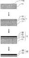
도 1은 본 발명의 적층체의 제조 공정의 한 형태를 나타내는 개략도이다.BRIEF DESCRIPTION OF THE DRAWINGS It is a schematic diagram which shows one form of the manufacturing process of the laminated body of this invention.
본 발명의 광학 소자의 제조 방법은 도 1에 나타내는 바와 같이, 최표면이 질화 알루미늄 단결정면(11a)인 질화 알루미늄 시드기판(11) 상에, 화학 기상 성장법에 의해 질화 알루미늄 단결정층(12)를 형성하는 제1 공정과, 상기 질화 알루미늄 단결정층(12) 상에 광학 소자층(20)을 형성하여 광학 소자용 적층체(2)를 얻는 제2 공정과, 상기 광학 소자용 적층체(2)로부터 상기 질화 알루미늄 시드기판(11)을 제거하는 제3 공정을 포함한다.In the manufacturing method of the optical element of this invention, as shown in FIG. 1, on the aluminum
(제1 공정)(First step)
본 발명의 제1 공정에서는 동시드기판인 질화 알루미늄 시드기판(11) 상에, 화학 기상 성장법에 의해 질화 알루미늄 단결정층(12)를 형성하여 제1 적층체(자립 기판)(1)을 얻는다.In the first step of the present invention, the aluminum nitride
최표면이 질화 알루미늄 단결정면(11a)인 질화 알루미늄 시드기판(11)의 제조 방법에는 특별히 한정은 없고, 공지된 방법이 이용된다. 예를 들면, 질화 알루미늄 시드기판(11)은 화학 기상 성장법에 의해 제작되어 최표면에 질화 알루미늄 단결정면을 갖는 질화 알루미늄 기판이라도 좋고, 승화법 등의 물리 기상법에 의해 제작된 질화 알루미늄 단결정 기판이라도 좋다.The manufacturing method of the aluminum
본 발명의 한 실시 형태로서 화학 기상 성장법에 의해 제작되고, 최표면에 질화 알루미늄 단결정면을 갖는 질화 알루미늄 단결정 시드기판에 대하여 이하에 설명한다.As one embodiment of the present invention, an aluminum nitride single crystal seed substrate produced by a chemical vapor deposition method and having an aluminum nitride single crystal surface on its outermost surface will be described below.
화학 기상 성장법에 의해 제작되고, 최표면이 질화 알루미늄 단결정면의 질화 알루미늄 시드기판으로서는, 예를 들면 일본 공개특허공보 제2010-89971에 제안되는 질화 알루미늄 단결정 기판을 이용해도 좋다. 또한, WO2009/090821, 일본 공개특허공보 제2010-10613에 제안되는 질화 알루미늄 비단결정층을 포함하는 질화 알루미늄계 적층체를 이용해도 좋다.As an aluminum nitride seed substrate produced by a chemical vapor deposition method and whose outermost surface is an aluminum nitride single crystal surface, for example, an aluminum nitride single crystal substrate proposed in JP-A-2010-89971 may be used. Moreover, you may use the aluminum nitride type laminated body containing the aluminum nitride non-single-crystal layer proposed by WO2009 / 090821 and Unexamined-Japanese-Patent No. 2010-10106.
이와 같은 화학 기상 성장법으로 제작되는 시드기판 중에서도, 시드기판 자체의 생산성, 하기에 상술하는 제3 공정의 실시의 용이함을 고려하면, 질화 알루미늄 비단결정층을 포함하는 질화 알루미늄계 적층체를 이용하는 것이 바람직하다. 구체적으로는 다결정, 비정질 또는 이것들의 혼합으로 이루어지는 질화 알루미늄 비단결정층 상에, 최표면을 형성하는 질화 알루미늄 단결정 박막층이 적층된 질화 알루미늄계 적층체를 이용하는 것이 바람직하다. 또한 해당 질화 알루미늄계 적층체의 생산성, 최표면의 결정성을 고려하면 최표면을 형성하는 질화 알루미늄 단결정 박막층의 두께가 10nm 이상 1.5㎛ 이하이며, 해당 질화 알루미늄 비단결정층의 두께가 해당 질화 알루미늄 단결정 박막층의 100배 이상인 질화 알루미늄계 적층체를 이용하는 것이 바람직하다.Among the seed substrates produced by such a chemical vapor deposition method, considering the productivity of the seed substrate itself and the ease of carrying out the third process described below, it is preferable to use an aluminum nitride based laminate including an aluminum nitride non-single crystal layer. desirable. Specifically, it is preferable to use an aluminum nitride based laminate in which an aluminum nitride single crystal thin film layer forming an outermost surface is laminated on an aluminum nitride non-single crystal layer composed of polycrystal, amorphous or a mixture thereof. In consideration of the productivity and crystallinity of the outermost surface of the aluminum nitride-based laminate, the thickness of the aluminum nitride single crystal thin film layer forming the outermost surface is 10 nm or more and 1.5 µm or less, and the thickness of the aluminum nitride non-single crystal layer is the aluminum nitride single crystal. It is preferable to use the aluminum nitride based laminate which is 100 times or more of the thin film layer.
이와 같은 질화 알루미늄계 적층체는 비단결정층을 가지기 때문에, 자외선 투과율은 낮고 광학 소자의 구성 부재로서는 부적당하지만, 본 발명에서는 시드기판 자체가 제조 과정에서 제거되기 때문에, 최종 제품이 되는 광학 소자에 있어서 특별히 문제는 되지 않는다. 또한, 사파이어 기판 등의 이(異)시드기판과는 다르며, 같은 질화 알루미늄으로 이루어지는 적층체이기 때문에, 열팽창 계수차가 작다고 하는 이점도 있다. 또한 비단결정층은 제3 공정으로 제거하기 쉽다는 이점도 있다.Since such an aluminum nitride-based laminate has a non-single crystal layer, the UV transmittance is low and unsuitable as a constituent member of the optical element. However, in the present invention, the seed substrate itself is removed in the manufacturing process, and thus, in the optical element to be a final product. It is not a problem in particular. Moreover, since it is a laminated body which differs from two-seed substrates, such as a sapphire substrate, and consists of the same aluminum nitride, there exists also an advantage that a thermal expansion coefficient difference is small. In addition, there is an advantage that the non-single crystal layer is easy to remove in the third step.
상기와 같은 질화 알루미늄 시드기판(11)의 최표면에 위치하는 질화 알루미늄 단결정면(11a) 상에, 화학 기상 성장법에 의해 질화 알루미늄 단결정층(12)를 형성하는 방법에는 특별히 한정은 없으며 공지된 방법이 이용된다. 화학 기상 성장법으로서는 HVPE법 등이 일반적이다.The method of forming the aluminum nitride
이와 같이하여 얻어지는 질화 알루미늄 단결정층(12)는 파장 240nm부터 300nm에 있어서의 흡수 계수가 30cm-1이하로 낮고, 전위 밀도는 109cm-2이하로 할 수 있다.The aluminum nitride
또한, 제1 공정에 있어서 형성되는 질화 알루미늄 단결정층(12)의 두께는 제조 코스트의 관점에서는 얇을수록 좋지만, 제조 공정에 있어서의 핸들링을 용이하게 하고, 또한 크랙 등의 발생에 의한 제품 수율 저하를 억제한다는 관점에서, 50㎛ 이상인 것이 바람직하고 실용적인 관점 등에서 더 바람직하게는 100~300㎛, 특히 100~250㎛인 것이 바람직하다.In addition, although the thickness of the aluminum nitride
본 발명에 의하면, 질화 알루미늄 단결정층(12)의 두께를 500㎛ 이하, 또한 300㎛ 이하, 특히 250㎛ 이하로 해도 제조 공정에 있어서의 핸들링을 용이하게 할 수 있다. 이것은 광학 소자층(20)이 최종적으로 제거되는 질화 알루미늄 시드기판(11)을 갖는 제1 적층체(자립 기판) 상에 형성되기 때문이다. 즉, 질화 알루미늄 시드기판(11)을 갖기 때문에, 질화 알루미늄 단결정층(12)의 두께가 얇아도, 제1 적층체(자립 기판)가 충분한 강도를 갖기 때문이다. 또한 본 발명에 의해 얻어지는 광학 소자(22)는 비교적 얇은 두께의 질화 알루미늄 단결정층(12)를 갖기 때문에 자외선 투과율을 높일 수 있다. 질화 알루미늄 단결정층(12)가 두꺼워지면 자외선을 투과하기 어려워지지만, 본 발명의 방법에 의하면 해당 단결정층(12)를 얇게 할 수 있기 때문에, 이 점에서도 유리하게 된다.According to the present invention, even when the thickness of the aluminum nitride
본 발명에 있어서, 질화 알루미늄 시드기판(11)의 두께도 특별히 제한되는 것은 아니지만, 하기에 상술하는 광학 소자 적층체의 생산성, 핸들링성 및 제3 공정의 용이함을 고려하면, 100~500㎛인 것이 바람직하다. 또한 해당 시드기판으로서 상기 질화 알루미늄계 적층체를 사용하였을 경우에는 해당 적층체 자체의 두께가 상기 범위를 만족하는 것이 바람직하다.In the present invention, the thickness of the aluminum
또한, 질화 알루미늄 단결정층(12)의 형성 후의 표면 거칠기는 특별히 한정되는 것은 아니다. 다만, 질화 알루미늄 단결정층(12)의 성장 직후의 표면이 거칠고, 그에 따라 제2 공정에 있어서 형성되는 광학 소자층의 성능을 저하시키는 경우는, 제1 공정 종료 후에 질화 알루미늄 단결정층(12)의 표면 연마를 실시하여 표면을 평활하게 하는 것이 바람직하다. 제2 공정으로 고품질의 광학 소자층을 얻기 위해서는, 질화 알루미늄 단결정층(12)의 표면 거칠기가 제곱 평균 거칠기(RMS치)로 5nm 이하인 것이 바람직하고, 더욱 1nm 이하인 것이 바람직하다. 이 연마를 실시하는 경우도, 시드기판 부분을 갖는 기판을 취급하기 때문에 충분한 강도를 가지며 연마를 용이하게 실시할 수 있다.In addition, the surface roughness after formation of the aluminum nitride
(제2 공정)(Second Step)
본 발명의 제2 공정에서는, 제1 공정으로 얻어진 제1 적층체(자립 기판)(1) 상에 광학 소자층(20)을 형성하여, 제2의 적층체 즉 광학 소자용 적층체(2)를 얻는다.In the 2nd process of this invention, the
질화 알루미늄 단결정층(12) 상에 광학 소자층(20)을 형성하는 방법에는, 특별히 한정은 없고 공지된 방법이 이용된다. 통상은 광학 소자층(20)은 MOCVD법 등의 화학 기상 성장법에 의해 형성된다.The method for forming the
본 발명의 한 실시 형태로서 MOCVD법에 의한 광학 소자층(20)의 형성에 대하여 이하에 설명한다.As an embodiment of the present invention, formation of the
MOCVD법은 유기 금속 III족 원료 가스와 질소원 원료 가스를 기판 상에 공급하여, 해당 기판 상에 III족 질화물 단결정층을 성장시키는 것이다. 본 발명에서 사용하는 원료 가스는, 목적으로 하는 III족 질화물 단결정층의 조성에 따라서, 공지된 원료가 특별히 제한 없이 사용될 수 있다. 구체적으로는 III족 원료 가스로서는 트리메틸알루미늄, 트리에틸알루미늄, 트리메틸갈륨, 트리에틸갈륨 또는 트리메틸인듐의 가스를 사용하는 것이 바람직하다. 또한 이것들 III족 원료는 성장시키는 III족 질화물 단결정층의 조성에 따라서, 그 원료의 종류, 사용 비율을 적당하게 결정하면 좋다. 또한, 질소원 가스로서는 암모니아 가스를 사용하는 것이 바람직하다. 또한 전도성의 제어를 목적으로 하여 첨가하는 불순물 원료 가스로서는 P형 불순물 원료 가스로서 비스시클로펜타디엔일마그네슘, N형 불순물 원료 가스로서 모노실란 또는 테트라에틸실란을 이용하는 것이 바람직하다. 또한, 본 발명에서 사용하는 MOCVD 장치에 대해서는, 본 발명을 실시할 수 있는 구조이면 특별히 제한되는 것은 아니며, 공지된 장치 또는 시판되는 MOCVD 장치를 이용할 수 있다.
In the MOCVD method, an organometallic Group III source gas and a nitrogen source source gas are supplied onto a substrate to grow a Group III nitride single crystal layer on the substrate. The raw material gas used by this invention can use a well-known raw material without a restriction | limiting especially according to the composition of the target group III nitride single crystal layer. Specifically, it is preferable to use gas of trimethyl aluminum, triethyl aluminum, trimethyl gallium, triethyl gallium, or trimethyl indium as group III source gas. Moreover, what is necessary is just to determine suitably the kind and usage ratio of these raw materials of this Group III raw material according to the composition of the Group III nitride single crystal layer to grow. In addition, it is preferable to use ammonia gas as a nitrogen source gas. Moreover, it is preferable to use biscyclopentadienyl magnesium as a P-type impurity source gas, and monosilane or tetraethylsilane as an N-type impurity source gas as an impurity source gas added for the purpose of conductivity control. In addition, the MOCVD apparatus used in the present invention is not particularly limited as long as it is a structure capable of carrying out the present invention, and a known apparatus or a commercially available MOCVD apparatus can be used.
이하, 일반적인 광학 소자인 LED를 제조하는 예에 대하여 자세하게 설명한다. 또한, 이하에 설명하는 LED 구조는 기판 상에 N형 III족 질화물 반도체층, 활성층, P형 III족 질화물 반도체층, P형 III족 질화물 컨택트층을 차례로 적층시킨 구조를 예로 설명하고 있지만, 본 발명은 이하의 구조로 한정되는 것은 아니다.Hereinafter, the example which manufactures LED which is a general optical element is demonstrated in detail. In addition, although the LED structure demonstrated below demonstrates the structure which laminated | stacked the N type III nitride semiconductor layer, the active layer, the P type III nitride semiconductor layer, and the P type III nitride contact layer in order on the board | substrate as an example, this invention Is not limited to the following structures.
우선, 제1 공정에서 얻어진 제1 적층체(1)(자립 기판(1))을 MOCVD 장치 내에 설치한 후, 자립 기판(1)을 1050℃ 이상, 더 바람직하게는 1150℃ 이상으로 가열하여, 수소 분위기 중에 유지하는 것으로써 자립 기판 표면의 클리닝을 실시한 후, 트리메틸알루미늄, 트리메틸갈륨, 암모니아, 모노실란 또는 테트라에틸실란 및 원료 가스의 캐리어 가스로서 수소, 질소 등을 MOCVD 장치 내에 도입하여 N형 III족 질화물 반도체층을 형성한다.First, after installing the 1st laminated body 1 (independent substrate 1) obtained by the 1st process in a MOCVD apparatus, the
또한, 상기 N형 III족 질화물 반도체층을 형성하기 전에, N형 특성을 향상시키는 것을 목적으로 하여 버퍼층을 형성할 수도 있다. 이 경우, 버퍼층으로서는 해당 III족 질화물 반도체층 및 질화 알루미늄 단결정층과 동일 또는 중간의 격자 정수를 가지는 N형 III족 질화물층인 것이 바람직하다. 또한, 버퍼층은 단일층이라도 좋고 조성이 다른 복수의 적층체로 할 수도 있다.Further, before forming the N-type III-nitride semiconductor layer, a buffer layer may be formed for the purpose of improving the N-type characteristics. In this case, the buffer layer is preferably an N-type III-nitride layer having the same or intermediate lattice constant as the III-nitride semiconductor layer and the aluminum nitride single crystal layer. The buffer layer may be a single layer or a plurality of laminates having different compositions.
계속해서, 트리메틸알루미늄, 트리메틸갈륨, 암모니아 및 원료 가스의 캐리어 가스로서 수소, 질소 등을 MOCVD 장치 내에 도입하여 발광층이 되는 양자 우물 구조를 형성한다. 여기서, 양자 우물 구조란, 두께 수~수십nm의 우물층과 해당 우물층보다 밴드 갭 에너지가 큰 장벽층을 조합한 적층 구조이며, 상기 우물층의 밴드 갭 에너지나 장벽층 막두께 등은 원하는 광학 특성을 얻을 수 있도록 적당하게 설정하면 좋다. 또한, 상기 원료에 더하여, 광학 특성을 향상시키는 등의 목적으로 트리메틸인듐, N형 또는 P형 불순물 원료를 더해도 좋다.Subsequently, hydrogen, nitrogen or the like is introduced into the MOCVD apparatus as a carrier gas of trimethylaluminum, trimethylgallium, ammonia and source gas to form a quantum well structure serving as a light emitting layer. Here, the quantum well structure is a laminated structure in which a well layer having a thickness of several tens of nm and a barrier layer having a larger band gap energy than the well layer is combined, and the band gap energy, barrier layer film thickness, etc. of the well layer are desired optical. It is good to set it properly so that a characteristic can be obtained. In addition to the above-mentioned raw materials, trimethyl indium, N-type or P-type impurity raw materials may be added for the purpose of improving the optical properties.
계속해서, 트리메틸알루미늄, 트리메틸갈륨, 암모니아, 비스시클로펜타디엔일마그네슘 및 원료 가스의 캐리어 가스로서 수소, 질소 등을 MOCVD 장치 내에 도입하여, P형 III족 질화물 반도체층을 형성한다. 그 후, 트리메틸갈륨, 암모니아, 비스시클로펜타디엔일마그네슘 및 원료 가스의 캐리어 가스로서 수소, 질소 등을 MOCVD 장치 내에 도입하여, P형 III족 질화물 반도체 컨택트층을 형성한다. 여기서, 상기 III족 질화물 반도체층을 형성할 때 원료 공급비, 성장 온도, V족원소(질소등)와 III족 원소와의 비(V/III비) 등은, 원하는 광학 특성 및 전도 특성을 얻을 수 있도록 적당히 설정하면 좋다.Subsequently, hydrogen, nitrogen, or the like is introduced into the MOCVD apparatus as a carrier gas of trimethylaluminum, trimethylgallium, ammonia, biscyclopentadienylmagnesium and source gas to form a P-type III-nitride semiconductor layer. Thereafter, trimethylgallium, ammonia, biscyclopentadienylmagnesium, hydrogen, nitrogen, and the like are introduced into the MOCVD apparatus as carrier gases of the raw material gas to form a P-type III-nitride semiconductor contact layer. Here, when forming the group III nitride semiconductor layer, the raw material supply ratio, the growth temperature, the ratio of the group V element (nitrogen, etc.) and the group III element (V / III ratio), etc. obtain desired optical and conducting characteristics. It is good to set it properly.
또한, 본 발명의 광학 소자용 적층체(2)는 상기 제2 공정을 거쳐 얻어지는 중간 생성물이며, 질화 알루미늄 시드기판과 해당 질화 알루미늄 시드기판 상에 형성된 광학 특성이 뛰어난 질화 알루미늄 단결정층과 해당 질화 알루미늄 단결정층 상에 형성된 광학 소자를 포함한다. 본 발명의 광학 소자용 적층체(2)는 광학 소자의 제조 공정에 있어서, 그 이송, 보관 등을 용이하게 하여 제조 효율이 향상된다.Further, the
(제3 공정)(Third process)
본 발명의 제3 공정에서는 제2 공정에서 얻어진 광학 소자용 적층체(2)로부터 질화 알루미늄 시드기판(11)을 제거하여 광학 소자(22)를 얻는다.In the third process of this invention, the aluminum nitride seed board |
여기서, 상기의 프로세스에 의해 제조한 광학 소자(22)를 디바이스로서 기능시키기 위해서는, 소정의 전도층을 노출시키는 에칭 처리, 전도층 표면에의 전극 형성 처리 등 소자화를 위한 가공을 실시 할 필요가 있다. 본 발명의 제3 공정은 상기 소자화를 위한 가공 공정을 실시하기 전에 실시할 수도 있고, 소자화를 위한 가공을 실시한 후에 실시할 수도 있다. 소자화를 위한 가공 공정과 본 발명의 제3 공정을 실시하는 순서는 생산성이나 핸들링성 등을 고려하여 본 발명을 실시할 때 적당히 결정하면 좋다.Here, in order to function the
광학 소자용 적층체(2)로부터 질화 알루미늄 시드기판(11)을 제거하는 방법으로는 특별히 한정은 없으며, 연마, 반응성 이온 에칭, 알칼리 용액 등을 이용한 습식 에칭 등의 공지된 방법을 이용할 수 있지만, 연마에 의해 제거하는 것이 바람직하다.The method of removing the aluminum
또한, 상기 제3 공정 종료 후에, 상기 질화 알루미늄 시드기판(11)을 제거한 측의, 상기 질화 알루미늄 단결정층(12) 표면에 요철을 형성하는 것도, 해당 광학 소자의 성능을 향상시키는 수단으로서 매우 적합하게 이용할 수 있다. 예를 들면 LED에 상기 요철 형성 프로세스를 적용하였을 경우는, 해당 요철의 존재에 의해, 상기 기판 표면에서의 전체 반사량이 저감되어, 결과적으로 LED의 발광 특성을 향상시키는 것이 가능하게 된다.In addition, forming irregularities on the surface of the aluminum nitride
이와 같이 얻어진 광학 소자(22)는 필요에 따라 칩화 등의 처리가 실시되어 다양한 용도에 이용된다. 광학 소자로서는 예를 들면 LED(발광 다이오드) 등을 들 수 있다.The
상술한 본 발명의 한 실시 형태로써는 화학 기상 성장법에 의해 제작되는 동시드기판인 질화 알루미늄 단결정 시드기판(11) 상에, 화학 기상 성장법에 의해 질화 알루미늄 단결정층(12)를 형성하여 제1 적층체(자립 기판)(1)을 준비한다. 이 때, 해당 질화 알루미늄 단결정 시드기판(11)의 전위 밀도가 낮기 때문에, 질화 알루미늄 단결정층(12) 및 그 위에 형성되는 광학 소자층(20)에 있어서도 전위 밀도의 저감이 가능하게 된다. 뿐만 아니라, 해당 질화 알루미늄 단결정층(12)는 화학 기상 성장법에 의해 형성되기 때문에, 저전위 또는 높은 자외선 투과 효율을 실현할 수 있다. 또한, 해당 질화 알루미늄 단결정층(12)와 광학 소자층(20)과의 굴절 효율차가 작기 때문에, 광 추출 효율도 종래와 비교하여 향상된다.In one embodiment of the present invention described above, the aluminum nitride
또한 본 발명은 상술한 실시 형태로 한정되는 것은 아니고, 본 발명의 범위 내에서 다양하게 개변될 수 있다. 예를 들면, 질화 알루미늄 단결정 시드기판(11)은 상술한 화학 기상 성장법 이외에도, 승화법 등의 물리 기상 성장법에 따라 제작된 것이라도 좋다.In addition, this invention is not limited to embodiment mentioned above, It can variously change within the range of this invention. For example, the aluminum nitride single
또한, 예를 들면 상술한 실시 형태에서는 본 발명과 관련되는 광학 소자로서 자외 발광 소자를 예시했지만, 본 발명과 관련되는 전자 부품으로서는 발광 다이오드 소자 등의 발광 소자로 한정되지 않는다. 본 발명의 광학 소자의 제조 방법은 예를 들면 자외선으로부터 적외선까지의 폭넓은 영역의 감도를 갖는 반도체 소자를 밀봉한 수광 소자의 제조에도 응용할 수 있다.
For example, although the ultraviolet light emitting element was illustrated as the optical element which concerns on this invention in embodiment mentioned above, it is not limited to light emitting elements, such as a light emitting diode element, as an electronic component which concerns on this invention. The manufacturing method of the optical element of this invention is applicable also to manufacture of the light receiving element which sealed the semiconductor element which has the sensitivity of the wide area | region from ultraviolet-ray to infrared rays, for example.
[실시예][Example]
이하, 본 발명을 더욱 상세한 실시예에 근거하여 설명하지만, 본 발명은 이들 실시예로 한정되지 않는다.
EMBODIMENT OF THE INVENTION Hereinafter, although this invention is demonstrated based on further detailed Example, this invention is not limited to these Examples.
(질화 알루미늄 시드기판(11)의 준비)(Preparation of the aluminum nitride seed substrate 11)
질화 알루미늄 시드기판(11)은 WO2009/090821에 기재된 방법에 의해 제작하였다. 이 질화 알루미늄 시드기판(11)은 질화 알루미늄 단결정면(11a)를 구성하는 질화 알루미늄 단결정 박막층의 두께가 200nm이며, 그 아래의 질화 알루미늄 비단결정층(질화 알루미늄 다결정층)의 두께가 300㎛인 적층체를 이용하였다. 또한, 이 질화 알루미늄 시드기판(11)은 8mm 각(角)인 것을 2매 준비하였다.The aluminum
(제1 공정)(First step)
2매의 상기 질화 알루미늄 시드기판(11)을 질화 알루미늄 단결정면(11a)가 최표면이 되도록 HVPE 장치내의 서셉터 상에 설치한 후, 수소를 10slm, 암모니아를 200sccm의 유량으로 흘리면서, 해당 질화 알루미늄 시드기판(11)을 1450℃로 가열하여, 20분간 유지함으로써 표면 클리닝을 실시하였다. 계속해서, 500℃로 가열한 금속 알루미늄과 염화수소 가스를 반응시켜 얻어진 3염화 알루미늄 가스 5sccm, 암모니아 가스 15sccm, 캐리어 가스로서 질소 1500sccm, 수소 5000sccm를 질화 알루미늄 시드기판(11) 상에 공급하여, 질화 알루미늄 단결정층(12)를 150㎛ 성장시켰다.After the two aluminum
질화 알루미늄 단결정층(12)의 표면을 미분 간섭 광학 현미경으로 관찰하여, 어느 샘플도 질화 알루미늄 단결정층(12)의 표면이 크랙 프리인 것을 확인하였다. 또한, 질화 알루미늄 단결정층(12)의 표면은 국소적으로는 매우 평탄하지만, 8mm 각 전체로서는 비교적 큰 요철이 기판 전면에 존재하고 있는 상태였다.The surface of the aluminum nitride
(질화 알루미늄 단결정층(12)의 연마 및 평가)(Abrasive and Evaluation of Aluminum Nitride Single Crystal Layer 12)
계속해서, 상기 질화 알루미늄 단결정층(12)의 표면을 CMP(Chemical Mechanical Polishing) 연마에 의해, RMS치가 1nm 이하로 될 때까지 연마하여 제1 적층체(1)(자립 기판(1))을 얻었다.Subsequently, the surface of the aluminum nitride
여기서, 제작한 자립 기판(1)의 1매에 대하여 질화 알루미늄 단결정층(12)의 특성을 평가하기 위해, 이면의 질화 알루미늄 비단결정층(질화 알루미늄 다결정층)을 기계 연마에 의해 제거하고, 그 후 CMP 연마에 의해 RMS치가 5nm 이하로 될 때까지 연마하는 것으로써, 대략 양면 경면 상태의 질화 알루미늄 단결정층(12)의 단체(單體)를 추출하였다. 연마 후의 질화 알루미늄 단결정층(12)의 막 두께는 100㎛였다. 투과형 전자 현미경을 이용한 평면 관찰에 의하여(가속 전압 300kV), 연마 후의 질화 알루미늄 단결정층(12) 표면의 관통 전위 밀도를 측정한 바 3×108cm-2였다. 또한, 자외 가시 분광광도계(시마즈 세이사쿠쇼제 UV-2550)에 의해, 해당 질화 알루미늄 단결정층(12)의 투과율을 측정한 바 파장 240nm부터 350nm에 있어서의 외부 투과율은 40% 이상이었다. 또한, 질화 알루미늄 단결정의 굴절률을 2.4로 하여, 상기 막 두께와 투과율로부터 흡수 계수를 산출한 바 파장 240nm부터 350nm에 있어서의 흡수 계수는 20cm-1 이하였다.Here, in order to evaluate the properties of the aluminum nitride
(제2 공정)(Second Step)
계속해서, 제1 적층체(1)(자립 기판(1)) 1매를, 연마된 질화 알루미늄 단결정층(12) 표면이 최표면이 되도록 MOCVD 장치내의 서셉터 상에 설치하였다. 그 후, 수소를 13slm의 유량으로 흘리면서 해당 자립 기판(1)을 1250℃까지 가열하여 10분간 유지하는 것으로 표면 클리닝을 실시하였다.Subsequently, one sheet of the first laminate 1 (independent substrate 1) was provided on the susceptor in the MOCVD apparatus so that the polished aluminum nitride
계속해서, 자립 기판(1)의 온도를 1200℃으로 하여, 트리메틸알루미늄 유량이 25㎛ol/min, 암모니아 유량이 1slm, 전체 유량이 10slm, 압력이 50Torr의 조건으로, 해당 질화 알루미늄 단결정층(12) 상에 질화 알루미늄 버퍼층을 두께 0.1㎛ 형성하였다. 계속해서, 서셉터상의 기판 온도를 1120℃으로 하여, 트리메틸 갈륨 유량이 20㎛ol/min, 트리메틸알루미늄이 35㎛ol/min, 암모니아 유량이 1.5slm, 전체 유량이 10slm, 압력이 50Torr의 조건으로 Al0.7Ga0.3N버퍼층을 0.2㎛ 형성하였다. 또한, 테트라에틸실란 3nmol/min를 동시에 공급한 이외는 버퍼층과 동조건으로 N형 Al0.7Ga0.3N층을 1.2㎛ 형성하였다.Subsequently, the temperature of the
계속해서, 트리메틸갈륨 유량을 40㎛ol/min, 트리메틸알루미늄을 3㎛ol/min로 한 이외는 버퍼층과 동조건으로 Al0.3Ga0.7N우물층을 2nm 형성하였다. 계속해서, 버퍼층과 동조건으로 장벽층을 15nm 형성하였다. 이 우물층과 장벽층의 성장을 3회 반복하는 것으로 3중량자 우물층을 형성하였다.Subsequently, trimethylgallium flow rate was except that the 40㎛ol / min, trimethylaluminum to 3㎛ol / min forming a 2nm Al0.3 Ga0.7 N well layer with the buffer layer and the same conditions. Subsequently, 15 nm of barrier layers were formed under the same conditions as the buffer layer. The growth of the well layer and the barrier layer was repeated three times to form a three-weight well layer.
계속해서, 트리메틸 갈륨 유량을 15㎛ol/min로 하여, 비스시클로펜타디엔일마그네슘 0.8㎛ol/min를 동시에 공급한 이외는 버퍼층과 동조건으로 P형 Al0.8Ga0.2N층을 20nm형성하였다. 계속해서, 트리메틸갈륨 유량을 40㎛ol/min, 비스시클로펜타디엔일마그네슘 0.3㎛ol/min, 암모니아 유량이 2.0 slm, 전체 유량이 8slm, 압력이 150Torr의 조건으로 P형GaN 컨택트층을 0.2㎛ 형성하였다. 이 기판을 MOCVD 장치로부터 추출하여 질소 분위기중 20분간, 800℃의 조건으로 열처리를 실시하였다.Next, trimethyl gallium and the flow rate in 15㎛ol / min, bis cyclopentadienyl magnesium other than those supplying 0.8㎛ol / min at the same time, the buffer layer and the same conditions as the P-type Al0.8 Ga0.2 N layer 20 nm was formed. Subsequently, the P-type GaN contact layer was 0.2 µm under the conditions of 40 µm / min of trimethylgallium flow rate, 0.3 µm / min of biscyclopentadienyl magnesium, 2.0 slm of ammonia flow rate, 8 slm of total flow rate, and 150 Torr pressure. Formed. The substrate was extracted from the MOCVD apparatus and heat-treated under conditions of 800 ° C. for 20 minutes in a nitrogen atmosphere.
계속해서, ICP 에칭 장치에 의해 해당 기판의 일부를 Si도핑 Al0.7Ga0.3N층이 노출할 때까지 에칭 한 후, 해당 노출 표면에 진공 증착법에 의해 Ti(20nm)/Al(100nm)/Ti(20nm)/Au(50nm) 전극을 형성하고, 질소 분위기 중 1분간, 1000℃의 조건으로 열처리를 실시하였다. 계속해서, 상기 P형 GaN 컨택트층 상에 진공 증착법에 의해 Ni(20nm)/Au(100nm) 전극을 형성하여, 질소 분위기 중 5분간, 500℃의 조건으로 열처리를 실시하였다.Subsequently, Si-doped portions of the substrate by the ICP etching apparatus Al0.7 Ga0.3 N layer is etched until after exposure, Ti (20nm) by vacuum deposition on the exposed surface / Al (100nm ) / Ti (20 nm) / Au (50 nm) electrode was formed, and heat-processing was performed on 1000 degreeC conditions for 1 minute in nitrogen atmosphere. Subsequently, a Ni (20 nm) / Au (100 nm) electrode was formed on the P-type GaN contact layer by vacuum deposition, and heat treatment was performed at 500 ° C. for 5 minutes in a nitrogen atmosphere.
이상과 같이 하여, 제1 적층체의 질화 알루미늄 단결정층(12) 상에, 광학 소자층(20)이 적층된 제2 적층체(2)(광학 소자용 적층체(2))를 제작하였다. 이와 같이 하여 제작한 광학 소자용 적층체(2)의 직류 10mA 동작 시에 있어서의 소자 이면으로부터 발광 특성을 평가한 바, 발광 파장 265nm의 미약한 싱글 발광 피크를 확인할 수 있었다.As mentioned above, the 2nd laminated body 2 (the optical element laminated body 2) in which the
(제3 공정)(Third process)
상기 광학 소자용 적층체(2)의 이면의 질화 알루미늄 비단결정층(질화 알루미늄 다결정층)을 기계 연마에 의해 제거하고, 그 후 CMP 연마에 의해 RMS치가 5nm이하로 될 때까지 연마하여 광학 소자(22)를 제작하였다. 또한, 이 광학 소자(22)의 두께는 약 100㎛였다. 이 광학 소자(22)를 광학 소자용 적층체(2)와 같은 방법으로 발광 측정을 실시한 바, 발광 파장 265nm의 싱글 피크 발광이며, 이 광학 소자(22)의 발광 피크 강도는 광학 소자용 적층체(2)의 강도보다 10배 이상인 것이 확인되었다.The aluminum nitride non-single crystal layer (aluminum nitride polycrystalline layer) on the back surface of the laminate for
2 : 제2의 적층체(광학 소자용 적층체)
1 : 제1 적층체(자립 기판)
11 : 질화 알루미늄 시드기판
11a : 질화 알루미늄 단결정면
12 : 질화 알루미늄 단결정층
20 : 광학 소자층
22 : 광학 소자2: 2nd laminated body (laminate for optical elements)
1: 1st laminated body (independent board | substrate)
11: aluminum nitride seed substrate
11a: aluminum nitride single crystal surface
12: aluminum nitride single crystal layer
20: optical element layer
22: optical element
Claims (6)
Translated fromKorean상기 질화 알루미늄 단결정층 상에, 광학 소자층을 형성하여 광학 소자용 적층체를 얻는 제2 공정과,
상기 광학 소자용 적층체로부터 상기 질화 알루미늄 시드기판을 제거하는 제3 공정을 포함하는 광학 소자의 제조 방법.A first step of forming an aluminum nitride single crystal layer by a chemical vapor deposition method on an aluminum nitride seed substrate made of aluminum nitride and whose outermost surface is an aluminum nitride single crystal surface;
A second step of forming an optical element layer on the aluminum nitride single crystal layer to obtain a laminate for optical elements;
And a third step of removing the aluminum nitride seed substrate from the laminate for optical elements.
상기 제1 공정에 있어서의 상기 질화 알루미늄 단결정층의 두께는 50㎛ 이상인 광학 소자의 제조 방법.The method of claim 1,
The thickness of the said aluminum nitride single crystal layer in a said 1st process is a manufacturing method of the optical element which is 50 micrometers or more.
상기 제2 공정에 있어서의 상기 광학 소자층은 LED 소자층인 것을 특징으로 하는 광학 소자의 제조 방법.3. The method according to claim 1 or 2,
The said optical element layer in a said 2nd process is a LED element layer, The manufacturing method of the optical element characterized by the above-mentioned.
상기 질화 알루미늄 시드기판 상에 형성된 질화 알루미늄 단결정층과,
상기 질화 알루미늄 단결정층 상에 형성된 광학 소자층을 갖는 광학 소자용 적층체.An aluminum nitride seed substrate composed of aluminum nitride and whose outermost surface is an aluminum nitride single crystal surface;
An aluminum nitride single crystal layer formed on the aluminum nitride seed substrate;
The laminated body for optical elements which has an optical element layer formed on the said aluminum nitride single crystal layer.
상기 질화 알루미늄 단결정층의 240nm부터 300nm에 있어서의 흡수 계수가 30cm-1 이하인 광학 소자용 적층체.5. The method of claim 4,
The laminated body for optical elements whose absorption coefficient in 240 nm-300 nm of the said aluminum nitride single crystal layer is 30 cm <-1> or less.
상기 질화 알루미늄 단결정층의 전위 밀도가 109cm-2 미만인 광학 소자용 적층체.
The method according to claim 4 or 5,
The laminated body for optical elements whose dislocation density of the said aluminum nitride single crystal layer is less than 109 cm <-2> .
Applications Claiming Priority (3)
| Application Number | Priority Date | Filing Date | Title |
|---|---|---|---|
| JP2010243824 | 2010-10-29 | ||
| JPJP-P-2010-243824 | 2010-10-29 | ||
| PCT/JP2011/073831WO2012056928A1 (en) | 2010-10-29 | 2011-10-17 | Method for manufacturing optical element |
Publications (2)
| Publication Number | Publication Date |
|---|---|
| KR20130122727Atrue KR20130122727A (en) | 2013-11-08 |
| KR101852519B1 KR101852519B1 (en) | 2018-04-26 |
Family
ID=45993643
Family Applications (1)
| Application Number | Title | Priority Date | Filing Date |
|---|---|---|---|
| KR1020137005745AActiveKR101852519B1 (en) | 2010-10-29 | 2011-10-17 | Method for manufacturing optical element |
Country Status (5)
| Country | Link |
|---|---|
| US (1) | US20130214325A1 (en) |
| EP (1) | EP2634294B1 (en) |
| JP (1) | JP5931737B2 (en) |
| KR (1) | KR101852519B1 (en) |
| WO (1) | WO2012056928A1 (en) |
Families Citing this family (6)
| Publication number | Priority date | Publication date | Assignee | Title |
|---|---|---|---|---|
| WO2014120637A1 (en)* | 2013-01-29 | 2014-08-07 | Hexatech, Inc. | Optoelectronic devices incorporating single crystalline aluminum nitride substrate |
| TWI717777B (en)* | 2014-11-10 | 2021-02-01 | 日商德山股份有限公司 | Apparatus for manufacturing group iii nitride single crystal, method for manufacturing group iii nitride single crystal using the same, and aluminum nitride single crystal |
| EP3267497A4 (en) | 2015-03-06 | 2018-10-10 | Stanley Electric Co., Ltd. | Group iii nitride laminate and light emitting element comprising said laminate |
| US10249786B2 (en)* | 2016-11-29 | 2019-04-02 | Palo Alto Research Center Incorporated | Thin film and substrate-removed group III-nitride based devices and method |
| WO2019079239A1 (en)* | 2017-10-16 | 2019-04-25 | Crystal Is, Inc. | Electrochemical removal of aluminum nitride substrates for electronic and optoelectronic devices |
| CN116194623A (en) | 2020-08-04 | 2023-05-30 | 株式会社德山 | Method for cleaning aluminum nitride single crystal substrate, method for manufacturing aluminum nitride single crystal laminate, method for manufacturing aluminum nitride single crystal substrate, and aluminum nitride single crystal substrate |
Family Cites Families (22)
| Publication number | Priority date | Publication date | Assignee | Title |
|---|---|---|---|---|
| JP4382748B2 (en)* | 2003-03-19 | 2009-12-16 | 独立行政法人科学技術振興機構 | Semiconductor crystal growth method |
| US7338555B2 (en)* | 2003-09-12 | 2008-03-04 | Tokuyama Corporation | Highly crystalline aluminum nitride multi-layered substrate and production process thereof |
| JP4592388B2 (en)* | 2004-11-04 | 2010-12-01 | シャープ株式会社 | III-V compound semiconductor light emitting device and method for manufacturing the same |
| DE102005041643A1 (en)* | 2005-08-29 | 2007-03-01 | Forschungsverbund Berlin E.V. | Semiconductor method for producing an isolated semiconductor substrate uses a masking layer with holes and an output layer |
| JP2009519202A (en)* | 2005-12-12 | 2009-05-14 | キーマ テクノロジーズ, インク. | Group III nitride product and method for producing the same |
| JP4862442B2 (en)* | 2006-03-15 | 2012-01-25 | 日立電線株式会社 | Method for manufacturing group III-V nitride semiconductor substrate and method for manufacturing group III-V nitride device |
| US8012257B2 (en)* | 2006-03-30 | 2011-09-06 | Crystal Is, Inc. | Methods for controllable doping of aluminum nitride bulk crystals |
| US9034103B2 (en)* | 2006-03-30 | 2015-05-19 | Crystal Is, Inc. | Aluminum nitride bulk crystals having high transparency to ultraviolet light and methods of forming them |
| JP5099008B2 (en)* | 2006-07-26 | 2012-12-12 | 富士通株式会社 | Compound semiconductor device using SiC substrate and manufacturing method thereof |
| WO2008054994A2 (en)* | 2006-10-18 | 2008-05-08 | Nitek, Inc. | Deep ultraviolet light emitting device and method for fabricating same |
| WO2008067537A2 (en)* | 2006-11-30 | 2008-06-05 | University Of South Carolina | Method and apparatus for growth of iii-nitride semiconductor epitaxial layers |
| US8080833B2 (en)* | 2007-01-26 | 2011-12-20 | Crystal Is, Inc. | Thick pseudomorphic nitride epitaxial layers |
| US8269251B2 (en)* | 2007-05-17 | 2012-09-18 | Mitsubishi Chemical Corporation | Method for producing group III nitride semiconductor crystal, group III nitride semiconductor substrate, and semiconductor light-emitting device |
| JP5262545B2 (en)* | 2007-10-29 | 2013-08-14 | 日立電線株式会社 | Nitride semiconductor free-standing substrate and device using the same |
| JP2009143778A (en)* | 2007-12-17 | 2009-07-02 | Sumitomo Metal Mining Co Ltd | Aluminum nitride crystal growth method, aluminum nitride substrate and semiconductor device |
| JP4996448B2 (en)* | 2007-12-25 | 2012-08-08 | パナソニック株式会社 | Method for creating a semiconductor substrate |
| JPWO2009090821A1 (en)* | 2008-01-16 | 2011-05-26 | 国立大学法人東京農工大学 | Manufacturing method of laminate having Al-based group III nitride single crystal layer, stacked body manufactured by the manufacturing method, manufacturing method of Al-based group III nitride single crystal substrate using the stacked body, and aluminum nitride single Crystal substrate |
| JP2009190918A (en)* | 2008-02-13 | 2009-08-27 | New Japan Radio Co Ltd | Nitride semiconductor substrate manufacturing method and nitride semiconductor device manufacturing method |
| US9331240B2 (en)* | 2008-06-06 | 2016-05-03 | University Of South Carolina | Utlraviolet light emitting devices and methods of fabrication |
| JP2010010613A (en) | 2008-06-30 | 2010-01-14 | Tokuyama Corp | Laminate, substrate for manufacturing self-supporting substrate, self-supporting substrate, and manufacturing methods thereof |
| EP2253988A1 (en)* | 2008-09-19 | 2010-11-24 | Christie Digital Systems USA, Inc. | A light integrator for more than one lamp |
| JP5197283B2 (en) | 2008-10-03 | 2013-05-15 | 国立大学法人東京農工大学 | Aluminum nitride single crystal substrate, laminate, and manufacturing method thereof |
- 2011
- 2011-10-17KRKR1020137005745Apatent/KR101852519B1/enactiveActive
- 2011-10-17WOPCT/JP2011/073831patent/WO2012056928A1/enactiveApplication Filing
- 2011-10-17EPEP11836064.3Apatent/EP2634294B1/enactiveActive
- 2011-10-17JPJP2012540780Apatent/JP5931737B2/enactiveActive
- 2011-10-17USUS13/881,385patent/US20130214325A1/ennot_activeAbandoned
Also Published As
| Publication number | Publication date |
|---|---|
| KR101852519B1 (en) | 2018-04-26 |
| JPWO2012056928A1 (en) | 2014-03-20 |
| EP2634294A4 (en) | 2015-05-13 |
| EP2634294B1 (en) | 2020-04-29 |
| EP2634294A1 (en) | 2013-09-04 |
| WO2012056928A1 (en) | 2012-05-03 |
| US20130214325A1 (en) | 2013-08-22 |
| JP5931737B2 (en) | 2016-06-08 |
Similar Documents
| Publication | Publication Date | Title |
|---|---|---|
| US7811902B2 (en) | Method for manufacturing nitride based single crystal substrate and method for manufacturing nitride based light emitting diode using the same | |
| KR101067122B1 (en) | Method of manufacturing group III nitride semiconductor, method of manufacturing group III nitride semiconductor light emitting device and group III nitride semiconductor light emitting device, and lamp | |
| KR102062327B1 (en) | Aluminium nitride substrate and group-iii nitride laminate | |
| JP2004524250A (en) | Gallium nitride materials and methods | |
| KR102112249B1 (en) | Semiconductor wafer | |
| JP2006128626A (en) | Nitride semiconductor device and its manufacturing method | |
| CN111009602A (en) | Epitaxial substrate with 2D material interposer, preparation method and manufacturing assembly | |
| KR20130122727A (en) | Method for manufacturing optical element | |
| CN102465342B (en) | Method of manufacturing gan-based film | |
| JP5073624B2 (en) | Method for growing zinc oxide based semiconductor and method for manufacturing semiconductor light emitting device | |
| JP2009155141A (en) | Method for producing semiconductor substrate, semiconductor substrate and compound semiconductor light emitting device using the same | |
| JP2017208554A (en) | Semiconductor stack | |
| JP2009238772A (en) | Epitaxial substrate and method for manufacturing epitaxial substrate | |
| JP5551131B2 (en) | Manufacturing method of nitride semiconductor multilayer structure | |
| JP2005072310A (en) | Method for manufacturing group iii nitride compound semiconductor | |
| JP2004115305A (en) | Gallium nitride single crystal substrate, method of manufacturing the same, gallium nitride-based semiconductor device and light emitting diode | |
| JP2004119423A (en) | Gallium nitride crystal substrate, its producing process, gallium nitride based semiconductor device, and light emitting diode | |
| CN107359228A (en) | A kind of epitaxial wafer of light emitting diode and preparation method thereof | |
| KR20120094406A (en) | Substrate having stacked layers and method of fabricating the same | |
| CN118398731B (en) | Method for manufacturing semiconductor structure, semiconductor structure and semiconductor device | |
| WO2009116232A1 (en) | Compound semiconductor substrate, light emitting element using compound semiconductor substrate, and method for manufacturing compound semiconductor substrate | |
| WO2007078065A1 (en) | Gallium nitride-based compound semiconductor | |
| TW202307294A (en) | Epitaxial wafer for ultraviolet light-emitting element and manufacturing method thereof | |
| TWI596797B (en) | Gallium nitride-based crystal and semiconductor device manufacturing method, and light-emitting device and method of manufacturing the light-emitting device | |
| JP4963301B2 (en) | Manufacturing method of nitride semiconductor light emitting device |
Legal Events
| Date | Code | Title | Description |
|---|---|---|---|
| PA0105 | International application | Patent event date:20130306 Patent event code:PA01051R01D Comment text:International Patent Application | |
| AMND | Amendment | ||
| PG1501 | Laying open of application | ||
| PA0201 | Request for examination | Patent event code:PA02012R01D Patent event date:20160525 Comment text:Request for Examination of Application | |
| E902 | Notification of reason for refusal | ||
| PE0902 | Notice of grounds for rejection | Comment text:Notification of reason for refusal Patent event date:20170620 Patent event code:PE09021S01D | |
| AMND | Amendment | ||
| E601 | Decision to refuse application | ||
| PE0601 | Decision on rejection of patent | Patent event date:20171227 Comment text:Decision to Refuse Application Patent event code:PE06012S01D Patent event date:20170620 Comment text:Notification of reason for refusal Patent event code:PE06011S01I | |
| AMND | Amendment | ||
| PX0901 | Re-examination | Patent event code:PX09011S01I Patent event date:20171227 Comment text:Decision to Refuse Application Patent event code:PX09012R01I Patent event date:20170818 Comment text:Amendment to Specification, etc. Patent event code:PX09012R01I Patent event date:20131002 Comment text:Amendment to Specification, etc. | |
| PX0701 | Decision of registration after re-examination | Patent event date:20180413 Comment text:Decision to Grant Registration Patent event code:PX07013S01D Patent event date:20180321 Comment text:Amendment to Specification, etc. Patent event code:PX07012R01I Patent event date:20171227 Comment text:Decision to Refuse Application Patent event code:PX07011S01I Patent event date:20170818 Comment text:Amendment to Specification, etc. Patent event code:PX07012R01I Patent event date:20131002 Comment text:Amendment to Specification, etc. Patent event code:PX07012R01I | |
| X701 | Decision to grant (after re-examination) | ||
| GRNT | Written decision to grant | ||
| PR0701 | Registration of establishment | Comment text:Registration of Establishment Patent event date:20180420 Patent event code:PR07011E01D | |
| PR1002 | Payment of registration fee | Payment date:20180420 End annual number:3 Start annual number:1 | |
| PG1601 | Publication of registration | ||
| PR1001 | Payment of annual fee | Payment date:20210402 Start annual number:4 End annual number:4 | |
| PR1001 | Payment of annual fee | Payment date:20220323 Start annual number:5 End annual number:5 | |
| PR1001 | Payment of annual fee | Payment date:20240315 Start annual number:7 End annual number:7 |