KR20130122006A - Image display device and method for manufacturing the same - Google Patents
Image display device and method for manufacturing the sameDownload PDFInfo
- Publication number
- KR20130122006A KR20130122006AKR1020137026158AKR20137026158AKR20130122006AKR 20130122006 AKR20130122006 AKR 20130122006AKR 1020137026158 AKR1020137026158 AKR 1020137026158AKR 20137026158 AKR20137026158 AKR 20137026158AKR 20130122006 AKR20130122006 AKR 20130122006A
- Authority
- KR
- South Korea
- Prior art keywords
- panel
- liquid crystal
- protective panel
- crystal display
- resin composition
- Prior art date
- Legal status (The legal status is an assumption and is not a legal conclusion. Google has not performed a legal analysis and makes no representation as to the accuracy of the status listed.)
- Ceased
Links
- 238000004519manufacturing processMethods0.000titleabstractdescription23
- 238000000034methodMethods0.000titledescription16
- 230000001681protective effectEffects0.000abstractdescription136
- 239000004973liquid crystal related substanceSubstances0.000abstractdescription101
- 239000011342resin compositionSubstances0.000abstractdescription91
- 239000011347resinSubstances0.000abstractdescription45
- 229920005989resinPolymers0.000abstractdescription45
- 229920003023plasticPolymers0.000abstractdescription21
- 239000004033plasticSubstances0.000abstractdescription20
- 238000005452bendingMethods0.000abstractdescription14
- 230000002093peripheral effectEffects0.000abstractdescription14
- 230000004224protectionEffects0.000description32
- 239000000463materialSubstances0.000description28
- 239000011521glassSubstances0.000description14
- 230000035882stressEffects0.000description11
- 230000003746surface roughnessEffects0.000description10
- 239000003999initiatorSubstances0.000description7
- 239000000758substrateSubstances0.000description7
- 239000011248coating agentSubstances0.000description6
- 238000000576coating methodMethods0.000description6
- 229920003229poly(methyl methacrylate)Polymers0.000description6
- 239000004926polymethyl methacrylateSubstances0.000description6
- 230000008569processEffects0.000description6
- 238000003860storageMethods0.000description6
- IEVADDDOVGMCSI-UHFFFAOYSA-N2-hydroxybutyl 2-methylprop-2-enoateChemical compoundCCC(O)COC(=O)C(C)=CIEVADDDOVGMCSI-UHFFFAOYSA-N0.000description5
- 238000010586diagramMethods0.000description5
- 229920000642polymerPolymers0.000description5
- 238000003825pressingMethods0.000description5
- 125000006850spacer groupChemical group0.000description5
- 239000000853adhesiveSubstances0.000description4
- 230000001070adhesive effectEffects0.000description4
- 230000005484gravityEffects0.000description4
- 229920002587poly(1,3-butadiene) polymerPolymers0.000description4
- 229920001195polyisoprenePolymers0.000description4
- 150000003505terpenesChemical class0.000description4
- 235000007586terpenesNutrition0.000description4
- 238000002834transmittanceMethods0.000description4
- JMIZWXDKTUGEES-UHFFFAOYSA-N2,2-di(cyclopenten-1-yloxy)ethyl 2-methylprop-2-enoateChemical compoundC=1CCCC=1OC(COC(=O)C(=C)C)OC1=CCCC1JMIZWXDKTUGEES-UHFFFAOYSA-N0.000description3
- 239000004925Acrylic resinSubstances0.000description3
- 229920000178Acrylic resinPolymers0.000description3
- WOBHKFSMXKNTIM-UHFFFAOYSA-NHydroxyethyl methacrylateChemical compoundCC(=C)C(=O)OCCOWOBHKFSMXKNTIM-UHFFFAOYSA-N0.000description3
- 230000008859changeEffects0.000description3
- 210000002858crystal cellAnatomy0.000description3
- 230000007613environmental effectEffects0.000description3
- 230000006355external stressEffects0.000description3
- FPYJFEHAWHCUMM-UHFFFAOYSA-Nmaleic anhydrideChemical compoundO=C1OC(=O)C=C1FPYJFEHAWHCUMM-UHFFFAOYSA-N0.000description3
- 230000035699permeabilityEffects0.000description3
- 238000004611spectroscopical analysisMethods0.000description3
- 239000000126substanceSubstances0.000description3
- 238000000870ultraviolet spectroscopyMethods0.000description3
- NIXOWILDQLNWCW-UHFFFAOYSA-MAcrylateChemical compound[O-]C(=O)C=CNIXOWILDQLNWCW-UHFFFAOYSA-M0.000description2
- NIXOWILDQLNWCW-UHFFFAOYSA-Nacrylic acid groupChemical groupC(C=C)(=O)ONIXOWILDQLNWCW-UHFFFAOYSA-N0.000description2
- 239000002390adhesive tapeSubstances0.000description2
- 210000004027cellAnatomy0.000description2
- 239000011159matrix materialSubstances0.000description2
- 239000000178monomerSubstances0.000description2
- 230000003287optical effectEffects0.000description2
- 229920001187thermosetting polymerPolymers0.000description2
- 2390000129561-hydroxycyclohexylphenyl-ketoneSubstances0.000description1
- 208000030984MIRAGE syndromeDiseases0.000description1
- 230000006750UV protectionEffects0.000description1
- PSGCQDPCAWOCSH-OPQQBVKSSA-N[(1s,3r,4s)-4,7,7-trimethyl-3-bicyclo[2.2.1]heptanyl] prop-2-enoateChemical compoundC1C[C@]2(C)[C@H](OC(=O)C=C)C[C@H]1C2(C)CPSGCQDPCAWOCSH-OPQQBVKSSA-N0.000description1
- -1acrylChemical group0.000description1
- MQDJYUACMFCOFT-UHFFFAOYSA-Nbis[2-(1-hydroxycyclohexyl)phenyl]methanoneChemical compoundC=1C=CC=C(C(=O)C=2C(=CC=CC=2)C2(O)CCCCC2)C=1C1(O)CCCCC1MQDJYUACMFCOFT-UHFFFAOYSA-N0.000description1
- 238000005520cutting processMethods0.000description1
- 230000006866deteriorationEffects0.000description1
- 239000006185dispersionSubstances0.000description1
- 230000000694effectsEffects0.000description1
- 238000005401electroluminescenceMethods0.000description1
- SUPCQIBBMFXVTL-UHFFFAOYSA-Nethyl 2-methylprop-2-enoateChemical compoundCCOC(=O)C(C)=CSUPCQIBBMFXVTL-UHFFFAOYSA-N0.000description1
- 230000001771impaired effectEffects0.000description1
- 230000006872improvementEffects0.000description1
- 238000003780insertionMethods0.000description1
- 230000037431insertionEffects0.000description1
- 230000001678irradiating effectEffects0.000description1
- 239000007788liquidSubstances0.000description1
- 238000005259measurementMethods0.000description1
- 239000000203mixtureSubstances0.000description1
- 238000000465mouldingMethods0.000description1
- 239000005304optical glassSubstances0.000description1
- 239000003973paintSubstances0.000description1
- 229920002635polyurethanePolymers0.000description1
- 239000004814polyurethaneSubstances0.000description1
- 238000007639printingMethods0.000description1
- TVLSRXXIMLFWEO-UHFFFAOYSA-NprochlorazChemical compoundC1=CN=CN1C(=O)N(CCC)CCOC1=C(Cl)C=C(Cl)C=C1ClTVLSRXXIMLFWEO-UHFFFAOYSA-N0.000description1
- 238000007493shaping processMethods0.000description1
- MSFGZHUJTJBYFA-UHFFFAOYSA-Msodium dichloroisocyanurateChemical compound[Na+].ClN1C(=O)[N-]C(=O)N(Cl)C1=OMSFGZHUJTJBYFA-UHFFFAOYSA-M0.000description1
- 239000007787solidSubstances0.000description1
- 239000005341toughened glassSubstances0.000description1
- 230000009466transformationEffects0.000description1
- XLYOFNOQVPJJNP-UHFFFAOYSA-NwaterSubstancesOXLYOFNOQVPJJNP-UHFFFAOYSA-N0.000description1
Images


Classifications
- G—PHYSICS
- G02—OPTICS
- G02F—OPTICAL DEVICES OR ARRANGEMENTS FOR THE CONTROL OF LIGHT BY MODIFICATION OF THE OPTICAL PROPERTIES OF THE MEDIA OF THE ELEMENTS INVOLVED THEREIN; NON-LINEAR OPTICS; FREQUENCY-CHANGING OF LIGHT; OPTICAL LOGIC ELEMENTS; OPTICAL ANALOGUE/DIGITAL CONVERTERS
- G02F1/00—Devices or arrangements for the control of the intensity, colour, phase, polarisation or direction of light arriving from an independent light source, e.g. switching, gating or modulating; Non-linear optics
- G02F1/01—Devices or arrangements for the control of the intensity, colour, phase, polarisation or direction of light arriving from an independent light source, e.g. switching, gating or modulating; Non-linear optics for the control of the intensity, phase, polarisation or colour
- G02F1/13—Devices or arrangements for the control of the intensity, colour, phase, polarisation or direction of light arriving from an independent light source, e.g. switching, gating or modulating; Non-linear optics for the control of the intensity, phase, polarisation or colour based on liquid crystals, e.g. single liquid crystal display cells
- G02F1/133—Constructional arrangements; Operation of liquid crystal cells; Circuit arrangements
- G02F1/1333—Constructional arrangements; Manufacturing methods
- G02F1/133308—Support structures for LCD panels, e.g. frames or bezels
- G—PHYSICS
- G02—OPTICS
- G02F—OPTICAL DEVICES OR ARRANGEMENTS FOR THE CONTROL OF LIGHT BY MODIFICATION OF THE OPTICAL PROPERTIES OF THE MEDIA OF THE ELEMENTS INVOLVED THEREIN; NON-LINEAR OPTICS; FREQUENCY-CHANGING OF LIGHT; OPTICAL LOGIC ELEMENTS; OPTICAL ANALOGUE/DIGITAL CONVERTERS
- G02F1/00—Devices or arrangements for the control of the intensity, colour, phase, polarisation or direction of light arriving from an independent light source, e.g. switching, gating or modulating; Non-linear optics
- G02F1/01—Devices or arrangements for the control of the intensity, colour, phase, polarisation or direction of light arriving from an independent light source, e.g. switching, gating or modulating; Non-linear optics for the control of the intensity, phase, polarisation or colour
- G02F1/13—Devices or arrangements for the control of the intensity, colour, phase, polarisation or direction of light arriving from an independent light source, e.g. switching, gating or modulating; Non-linear optics for the control of the intensity, phase, polarisation or colour based on liquid crystals, e.g. single liquid crystal display cells
- G02F1/133—Constructional arrangements; Operation of liquid crystal cells; Circuit arrangements
- G02F1/1333—Constructional arrangements; Manufacturing methods
- G—PHYSICS
- G09—EDUCATION; CRYPTOGRAPHY; DISPLAY; ADVERTISING; SEALS
- G09F—DISPLAYING; ADVERTISING; SIGNS; LABELS OR NAME-PLATES; SEALS
- G09F9/00—Indicating arrangements for variable information in which the information is built-up on a support by selection or combination of individual elements
- G—PHYSICS
- G02—OPTICS
- G02F—OPTICAL DEVICES OR ARRANGEMENTS FOR THE CONTROL OF LIGHT BY MODIFICATION OF THE OPTICAL PROPERTIES OF THE MEDIA OF THE ELEMENTS INVOLVED THEREIN; NON-LINEAR OPTICS; FREQUENCY-CHANGING OF LIGHT; OPTICAL LOGIC ELEMENTS; OPTICAL ANALOGUE/DIGITAL CONVERTERS
- G02F1/00—Devices or arrangements for the control of the intensity, colour, phase, polarisation or direction of light arriving from an independent light source, e.g. switching, gating or modulating; Non-linear optics
- G02F1/01—Devices or arrangements for the control of the intensity, colour, phase, polarisation or direction of light arriving from an independent light source, e.g. switching, gating or modulating; Non-linear optics for the control of the intensity, phase, polarisation or colour
- G02F1/13—Devices or arrangements for the control of the intensity, colour, phase, polarisation or direction of light arriving from an independent light source, e.g. switching, gating or modulating; Non-linear optics for the control of the intensity, phase, polarisation or colour based on liquid crystals, e.g. single liquid crystal display cells
- G02F1/133—Constructional arrangements; Operation of liquid crystal cells; Circuit arrangements
- G02F1/1333—Constructional arrangements; Manufacturing methods
- G02F1/133308—Support structures for LCD panels, e.g. frames or bezels
- G02F1/133311—Environmental protection, e.g. against dust or humidity
- G—PHYSICS
- G02—OPTICS
- G02F—OPTICAL DEVICES OR ARRANGEMENTS FOR THE CONTROL OF LIGHT BY MODIFICATION OF THE OPTICAL PROPERTIES OF THE MEDIA OF THE ELEMENTS INVOLVED THEREIN; NON-LINEAR OPTICS; FREQUENCY-CHANGING OF LIGHT; OPTICAL LOGIC ELEMENTS; OPTICAL ANALOGUE/DIGITAL CONVERTERS
- G02F1/00—Devices or arrangements for the control of the intensity, colour, phase, polarisation or direction of light arriving from an independent light source, e.g. switching, gating or modulating; Non-linear optics
- G02F1/01—Devices or arrangements for the control of the intensity, colour, phase, polarisation or direction of light arriving from an independent light source, e.g. switching, gating or modulating; Non-linear optics for the control of the intensity, phase, polarisation or colour
- G02F1/13—Devices or arrangements for the control of the intensity, colour, phase, polarisation or direction of light arriving from an independent light source, e.g. switching, gating or modulating; Non-linear optics for the control of the intensity, phase, polarisation or colour based on liquid crystals, e.g. single liquid crystal display cells
- G02F1/133—Constructional arrangements; Operation of liquid crystal cells; Circuit arrangements
- G02F1/1333—Constructional arrangements; Manufacturing methods
- G02F1/133308—Support structures for LCD panels, e.g. frames or bezels
- G02F1/13332—Front frames
- G—PHYSICS
- G02—OPTICS
- G02F—OPTICAL DEVICES OR ARRANGEMENTS FOR THE CONTROL OF LIGHT BY MODIFICATION OF THE OPTICAL PROPERTIES OF THE MEDIA OF THE ELEMENTS INVOLVED THEREIN; NON-LINEAR OPTICS; FREQUENCY-CHANGING OF LIGHT; OPTICAL LOGIC ELEMENTS; OPTICAL ANALOGUE/DIGITAL CONVERTERS
- G02F1/00—Devices or arrangements for the control of the intensity, colour, phase, polarisation or direction of light arriving from an independent light source, e.g. switching, gating or modulating; Non-linear optics
- G02F1/01—Devices or arrangements for the control of the intensity, colour, phase, polarisation or direction of light arriving from an independent light source, e.g. switching, gating or modulating; Non-linear optics for the control of the intensity, phase, polarisation or colour
- G02F1/13—Devices or arrangements for the control of the intensity, colour, phase, polarisation or direction of light arriving from an independent light source, e.g. switching, gating or modulating; Non-linear optics for the control of the intensity, phase, polarisation or colour based on liquid crystals, e.g. single liquid crystal display cells
- G02F1/133—Constructional arrangements; Operation of liquid crystal cells; Circuit arrangements
- G02F1/1333—Constructional arrangements; Manufacturing methods
- G02F1/133308—Support structures for LCD panels, e.g. frames or bezels
- G02F1/133325—Assembling processes
- G—PHYSICS
- G02—OPTICS
- G02F—OPTICAL DEVICES OR ARRANGEMENTS FOR THE CONTROL OF LIGHT BY MODIFICATION OF THE OPTICAL PROPERTIES OF THE MEDIA OF THE ELEMENTS INVOLVED THEREIN; NON-LINEAR OPTICS; FREQUENCY-CHANGING OF LIGHT; OPTICAL LOGIC ELEMENTS; OPTICAL ANALOGUE/DIGITAL CONVERTERS
- G02F1/00—Devices or arrangements for the control of the intensity, colour, phase, polarisation or direction of light arriving from an independent light source, e.g. switching, gating or modulating; Non-linear optics
- G02F1/01—Devices or arrangements for the control of the intensity, colour, phase, polarisation or direction of light arriving from an independent light source, e.g. switching, gating or modulating; Non-linear optics for the control of the intensity, phase, polarisation or colour
- G02F1/13—Devices or arrangements for the control of the intensity, colour, phase, polarisation or direction of light arriving from an independent light source, e.g. switching, gating or modulating; Non-linear optics for the control of the intensity, phase, polarisation or colour based on liquid crystals, e.g. single liquid crystal display cells
- G02F1/133—Constructional arrangements; Operation of liquid crystal cells; Circuit arrangements
- G02F1/1333—Constructional arrangements; Manufacturing methods
- G02F1/133308—Support structures for LCD panels, e.g. frames or bezels
- G02F1/133331—Cover glasses
- G—PHYSICS
- G02—OPTICS
- G02F—OPTICAL DEVICES OR ARRANGEMENTS FOR THE CONTROL OF LIGHT BY MODIFICATION OF THE OPTICAL PROPERTIES OF THE MEDIA OF THE ELEMENTS INVOLVED THEREIN; NON-LINEAR OPTICS; FREQUENCY-CHANGING OF LIGHT; OPTICAL LOGIC ELEMENTS; OPTICAL ANALOGUE/DIGITAL CONVERTERS
- G02F2201/00—Constructional arrangements not provided for in groups G02F1/00 - G02F7/00
- G02F2201/50—Protective arrangements
- G02F2201/503—Arrangements improving the resistance to shock
- G—PHYSICS
- G02—OPTICS
- G02F—OPTICAL DEVICES OR ARRANGEMENTS FOR THE CONTROL OF LIGHT BY MODIFICATION OF THE OPTICAL PROPERTIES OF THE MEDIA OF THE ELEMENTS INVOLVED THEREIN; NON-LINEAR OPTICS; FREQUENCY-CHANGING OF LIGHT; OPTICAL LOGIC ELEMENTS; OPTICAL ANALOGUE/DIGITAL CONVERTERS
- G02F2201/00—Constructional arrangements not provided for in groups G02F1/00 - G02F7/00
- G02F2201/54—Arrangements for reducing warping-twist
- G—PHYSICS
- G02—OPTICS
- G02F—OPTICAL DEVICES OR ARRANGEMENTS FOR THE CONTROL OF LIGHT BY MODIFICATION OF THE OPTICAL PROPERTIES OF THE MEDIA OF THE ELEMENTS INVOLVED THEREIN; NON-LINEAR OPTICS; FREQUENCY-CHANGING OF LIGHT; OPTICAL LOGIC ELEMENTS; OPTICAL ANALOGUE/DIGITAL CONVERTERS
- G02F2202/00—Materials and properties
- G02F2202/28—Adhesive materials or arrangements
Landscapes
- Physics & Mathematics (AREA)
- Nonlinear Science (AREA)
- General Physics & Mathematics (AREA)
- Mathematical Physics (AREA)
- Chemical & Material Sciences (AREA)
- Crystallography & Structural Chemistry (AREA)
- Optics & Photonics (AREA)
- Engineering & Computer Science (AREA)
- Theoretical Computer Science (AREA)
- Liquid Crystal (AREA)
- Devices For Indicating Variable Information By Combining Individual Elements (AREA)
Abstract
Translated fromKoreanDescription
Translated fromKorean본 발명은, 액정 표시 패널 등의 화상 표시 패널을 갖는 화상 표시 장치 및 그 제조 방법에 관한 것이고, 특히, 화상 표시 패널과 투명한 보호 패널 사이에 수지 경화물이 개재되어 있는 화상 표시 장치 및 그 제조 방법의 개량에 관한 것이다.TECHNICAL FIELD The present invention relates to an image display device having an image display panel such as a liquid crystal display panel and a method for producing the same, and in particular, an image display device and a method for producing the resin cured product interposed between the image display panel and the transparent protective panel. It is about improvement of.
액정 표시 장치 등의 화상 표시 장치에서는, 화상 표시 패널의 손상 방지나 표면 보호 등을 목적으로 하고, 화상 표시 패널의 전면 (前面) 에 유리 패널이나 플라스틱 패널 등의 투명한 보호 패널을 설치하는 것이 실시되고 있다. 보다 구체적으로는, 예를 들어, 화상 표시 패널의 주연부 (周緣部) 에서 화상 표시 패널과 보호 패널 사이에 스페이서 등을 개재시킴으로써, 보호 패널이 화상 표시 패널에 대해 약간의 공극을 가진 상태에서 케이스 내에 장착되어 있다.In image display apparatuses, such as a liquid crystal display device, in order to prevent damage of an image display panel, surface protection, etc., providing transparent protection panels, such as a glass panel and a plastic panel, in the front of an image display panel is implemented, have. More specifically, for example, by interposing a spacer or the like between the image display panel and the protective panel at the periphery of the image display panel, the protective panel is placed in the case in a state where there is a slight gap with respect to the image display panel. It is installed.
그러나, 이와 같은 구조를 채용했을 경우, 화상 표시 패널과 보호 패널 사이의 공극의 존재에 의해, 광이 산란되고, 그 결과, 콘트라스트나 휘도가 저하되거나 하여 화상 품위가 손상된다는 문제가 발생되었다. 또, 이와 같이 공극이 존재하는 구조에서는, 보호 패널과 공기의 굴절률 상이에 의해 이들 계면에서 반사가 일어나고, 특히 옥외에서의 시인성에 곤란함이 발생된다.However, when such a structure is adopted, light is scattered due to the presence of voids between the image display panel and the protective panel, and as a result, there arises a problem that the image quality is impaired due to a decrease in contrast and luminance. Moreover, in the structure in which a space | gap exists in this way, reflection arises at these interfaces by the difference of the refractive index of a protective panel and air, and it becomes difficult especially in visibility outdoors.
이와 같은 상황에서, 화상 표시 패널과 보호 패널 사이에 수지를 충전하는 것이 제안되어 있다. 예를 들어, 특허문헌 1 에 기재된 액정 표시 장치에서는, 액정 표시 패널의 표면에 부착된 편광판 주위에 스페이서를 배치하고, 이 스페이서의 상부에 표면 보호 유리를 탑재함과 함께 편광판과 표면 보호 유리 사이에 기포가 발생되지 않도록 접착제를 충전시킴으로써, 액정 표시 패널 상에 상기 표면 보호 유리를 부착하였다.In such a situation, it is proposed to fill the resin between the image display panel and the protective panel. For example, in the liquid crystal display device of
특허문헌 2 에도, 화상 표시 패널과 보호 패널을 적어도 1 층 이상의 투명 점착재를 개재하여 밀착시킨 화상 표시 장치가 개시되어 있고, 투명 점착재의 두께와 주파수 분산으로 측정한 동적 점탄성 특성을 소정의 관계로 함으로써, 우수한 내충격성이 실현되는 것이 기재되어 있다.Also in
특허문헌 1 : 일본 공개특허공보 2005-55641호Patent Document 1: JP-A-2005-55641
특허문헌 2 : 일본 공개특허공보 2003-29644호Patent Document 2: Japanese Unexamined Patent Publication No. 2003-29644
그런데, 제조 비용이나 내충격성 등의 관점에서 말하면, 보호 패널에 유리 패널을 사용하는 것보다 플라스틱 패널을 사용하는 것이 유리하다. 유리 패널은 플라스틱 패널에 비해 고가이고 충격에도 약하다. 그래서, 아크릴 수지의 1 종인 폴리메틸메타크릴레이트 (PMMA) 에 의해 형성된 플라스틱 패널을 보호 패널로서 사용하는 것이 검토되고 있다.By the way, from a viewpoint of manufacturing cost, impact resistance, etc., it is advantageous to use a plastic panel rather than using a glass panel for a protection panel. Glass panels are more expensive and less susceptible to impact than plastic panels. Then, using the plastic panel formed of polymethyl methacrylate (PMMA) which is one type of acrylic resin as a protection panel is examined.
그러나, 보호 패널로서 플라스틱 패널을 사용하는 것은, 보호 패널이 휘는 문제를 초래하여 표시 품위가 저하되는 요인이 된다. 예를 들어, 화상 표시 패널과 플라스틱 패널 사이에 수지 조성물을 충전하여 경화시키면, 수지 조성물이 경화될 때 체적 수축에 의해 발생하는 내부 응력, 플라스틱 패널이 환경 온도 변화에 의해 휨으로써 발생하는 외부 응력, 나아가서는 플라스틱 패널 자체가 갖는 성형시의 잔류 응력 등이 화상 표시 패널에 가해진다. 이와 같은 내부 응력, 외부 응력 또는 잔류 응력이 화상 표시 패널에 가해지면, 화상 표시 패널이 액정 표시 패널인 경우에는, 액정층의 셀 갭이 나노 레벨로 변동되어 표시 불균일이 발생되는 원인이 된다. 특히, 보호 패널의 사이즈를 화상 표시 패널의 사이즈보다 크게 하여 보호 패널의 외주 부분에 차광부를 형성하는 경우가 있는데, 이와 같이, 보호 패널의 사이즈를 화상 표시 패널의 사이즈보다 크게 한 경우에는 표시 불균일의 발생 경향이 현저해진다. 또, 극단적인 경우에는, 보호 패널의 외주 부분이 휘어올라, 광 누출 등이 발생하는 경우도 있다.However, the use of a plastic panel as a protective panel causes a problem that the protective panel is bent, which causes deterioration of display quality. For example, when the resin composition is filled and cured between the image display panel and the plastic panel, internal stress caused by volumetric shrinkage when the resin composition is cured, external stress caused by bending of the plastic panel due to environmental temperature change, Furthermore, the residual stress at the time of shaping | molding which the plastic panel itself has, etc. are applied to an image display panel. When such an internal stress, an external stress or a residual stress is applied to the image display panel, when the image display panel is a liquid crystal display panel, the cell gap of the liquid crystal layer is changed to a nano level, which causes display unevenness. In particular, although the size of the protective panel is larger than that of the image display panel, a light shielding portion may be formed in the outer peripheral portion of the protective panel. Thus, when the size of the protective panel is larger than the size of the image display panel, The tendency to occur becomes remarkable. In extreme cases, the outer periphery of the protective panel may bend, resulting in light leakage or the like.
화상 표시 패널과 보호 패널 사이에 충전되는 수지 조성물의 체적 수축을 억제하기 위해, 저경화 수축률, 저탄성률의 수지 조성물을 사용하는 것도 시도되고 있는데, 보호 패널에 플라스틱 패널을 사용한 경우에는 반드시 충분하다고 할 수 없는 것이 실정이다. 이것은, 폴리메틸메타크릴레이트 패널 등의 플라스틱 패널이 환경 온도 변화에 의해 (특히 고온에 노출됨으로써) 쉽게 휘기 때문에, 화상 표시 패널과 보호 패널 사이에 충전된 수지 조성물을 열경화시킬 때에는 물론, 자외선 조사에 의해 경화시킬 때에도 고온이 되어 휨이 쉽게 발생되고, 또한, 경화 후에도 고온에 의해 휨이 쉽게 발생되기 때문이다.In order to suppress the volumetric shrinkage of the resin composition filled between the image display panel and the protective panel, it is also attempted to use a resin composition having a low curing shrinkage rate and a low elastic modulus. It is not possible. This is because plastic panels, such as polymethyl methacrylate panels, bend easily due to changes in environmental temperature (especially when exposed to high temperatures), and, of course, when irradiating the thermosetting resin composition filled between the image display panel and the protective panel, ultraviolet irradiation. This is because the curvature is easily generated due to the high temperature even when cured, and the curvature is easily generated by the high temperature even after curing.
본 발명은, 이와 같은 종래의 실정을 감안하여 제안된 것으로서, 플라스틱에 의해 형성되는 보호 패널의 휨을 최소한으로 억제할 수 있는 화상 표시 장치의 구조를 제공하는 것을 목적으로 하고, 나아가서는 화상 표시 장치의 제조 방법을 제공하는 것을 목적으로 한다.The present invention has been proposed in view of such a conventional situation, and an object of the present invention is to provide a structure of an image display device that can minimize the warpage of a protective panel formed of plastic. It is an object to provide a manufacturing method.
전술한 목적을 달성하기 위해, 본 발명의 제 1 화상 표시 장치는, 화상 표시 패널과 플라스틱에 의해 형성된 투명한 보호 패널이 수지 경화물을 개재하여 대향 배치되어 이루어지는 화상 표시 장치로서, 보호 패널의 외형 치수가 화상 표시 패널의 외형 치수보다 크게 이루어지고, 당해 외주연부가 고정 지그로 고정되어 있는 것을 특징으로 한다.In order to achieve the above object, the first image display device of the present invention is an image display device in which a transparent protective panel formed of an image display panel and a plastic is disposed to face each other via a cured resin, and the external dimensions of the protective panel. Is larger than the external dimensions of the image display panel, and the outer periphery is fixed with a fixing jig.
본 발명의 제 1 화상 표시 장치의 제조 방법은, 화상 표시 패널과 플라스틱에 의해 형성된 투명한 보호 패널을 수지 조성물을 개재하여 대향 배치하고, 그 수지 조성물을 경화시키는 공정을 포함하는 화상 표시 장치의 제조 방법으로서, 보호 패널의 외형 치수를 화상 표시 패널의 외형 치수보다 크게 하고, 보호 패널의 외주연부를 고정 지그로 고정시킨 상태에서 수지 조성물을 경화시키는 것을 특징으로 한다.The manufacturing method of the 1st image display apparatus of this invention is a manufacturing method of the image display apparatus including the process of arrange | positioning the image display panel and the transparent protective panel which consists of plastics through a resin composition, and hardening the resin composition. It is characterized by making the external dimension of a protective panel larger than the external dimension of an image display panel, and hardening a resin composition in the state which fixed the outer peripheral part of a protective panel with a fixing jig.
또, 본 발명의 제 2 화상 표시 장치는, 화상 표시 패널과 플라스틱에 의해 형성된 투명한 보호 패널이 수지 경화물을 개재하여 대향 배치되어 이루어지는 화상 표시 장치로서,Moreover, the 2nd image display apparatus of this invention is an image display apparatus by which the transparent display panel formed with the image display panel and the plastics is arrange | positioned facing through the resin hardened | cured material,
보호 패널의 외형 치수가 화상 표시 패널의 외형 치수와 대략 동등하고, 그 외형 치수와, 보호 패널 및 화상 표시 패널의 케이스의 내측 치수가 동등하고, 보호 패널의 대략 전체면이 수지 경화물에 의해 화상 표시 패널과 접착되어 있는 것을 특징으로 한다.The external dimensions of the protective panel are approximately equal to the external dimensions of the image display panel, and the external dimensions are equal to the internal dimensions of the case of the protective panel and the image display panel, and the substantially entire surface of the protective panel is imaged by the cured resin. It is characterized by adhering to a display panel.
본 발명의 제 2 화상 표시 장치의 제조 방법은, 화상 표시 패널과 플라스틱에 의해 형성된 투명한 보호 패널을 수지 조성물을 개재하여 대향 배치하고, 그 수지 조성물을 경화시키는 공정을 포함하는 화상 표시 장치의 제조 방법으로서,The manufacturing method of the 2nd image display apparatus of this invention is a manufacturing method of the image display apparatus including the process of opposingly arrange | positioning an image display panel and the transparent protective panel formed of plastic via a resin composition, and hardening the resin composition. As
보호 패널의 외형 치수를 화상 표시 패널의 외형 치수와 대략 동등하게 함과 함께, 그 외형 치수와, 보호 패널 및 화상 표시 패널의 케이스의 내측 치수를 대략 동등하게 하고,Make the external dimensions of the protective panel approximately equal to the external dimensions of the image display panel, and make the external dimensions and internal dimensions of the case of the protective panel and the image display panel approximately equal,
그 케이스 내에서 보호 패널의 대략 전체면이 수지 조성물과 접한 상태에서 그 수지 조성물을 경화시키는 것을 특징으로 한다.It is characterized by hardening the resin composition in the state which the substantially whole surface of a protective panel contacted with the resin composition in the case.
또한, 본 발명에 있어서, 보호 패널의 외형 치수가 화상 표시 패널의 외형 치수보다 크다는 것은, 평면에서 보았을 때 보호 패널과 화상 표시 패널을 겹칠 경우, 화상 표시 패널이 보호 패널 안에 포함되는 것을 말한다.In addition, in this invention, that the external dimension of a protective panel is larger than the external dimension of an image display panel means that an image display panel is included in a protective panel when the protective panel and an image display panel overlap in planar view.
전술한 바와 같이, 보호 패널의 사이즈가 화상 표시 패널의 사이즈보다 큰 경우에, 보호 패널의 외주연부에서 휨의 발생이 현저하다. 그래서, 본 발명의 제 1 화상 표시 장치 혹은 그 제조 방법에서는, 고정 지그를 이용하여 보호 패널의 외주연부를 고정시킨 상태에서, 자외선 조사 등에 의해 수지 조성물의 경화를 실시하고, 경화 후에도 외주연부를 고정 지그로 고정시킨다. 이로써, 보호 패널의 휨이 교정된 상태에서 수지 조성물을 경화시키고, 또한, 보호 패널이 휘지 않는 상태를 유지할 수 있게 된다.As described above, when the size of the protective panel is larger than the size of the image display panel, the occurrence of warpage is remarkable at the outer periphery of the protective panel. Therefore, in the 1st image display apparatus or its manufacturing method of this invention, in the state which fixed the outer peripheral part of a protective panel using a fixing jig, hardening of a resin composition is performed by ultraviolet irradiation etc., and an outer peripheral part is fixed even after hardening. Fix it with a jig. Thereby, the resin composition can be cured in a state where the deflection of the protective panel is corrected, and the protective panel can be maintained in a non-bending state.
한편, 본 발명의 제 2 화상 표시 장치 혹은 그 제조 방법에서는, 보호 패널의 사이즈와 화상 표시 패널의 사이즈와 그들 케이스의 사이즈에 주목하여, 보호 패널의 외형 치수와 화상 표시 패널의 외형 치수와 그들 케이스의 내측 치수를 대략 동등하게 하고, 보호 패널의 대략 전체면이 수지 경화물과 접한 상태에서 수지 조성물을 경화시키므로, 보호 패널의 외주연부가 개방된 상태 그대로 수지 경화되는 경우가 없어지고, 또한, 보호 패널과 화상 표시 패널을 수지 조성물을 개재하여 케이스 내에 끼워넣는 것만으로, 보호 패널이 휘어오르는 것이 그 보호 패널의 측면 (케이스와 접하고 있는 면) 으로부터 억제되므로, 보호 패널의 고정 조치를 각별하게 하지 않아도 보호 패널 전체면에서 균등하게 수지 경화되어 휨의 발생이 억제된다.On the other hand, in the second image display device or the manufacturing method of the present invention, attention is paid to the size of the protective panel, the size of the image display panel and the size of those cases, and the external dimensions of the protective panel, the external dimensions of the image display panel, and their cases. Since the inner dimensions of the protective panel were made substantially equal and the entire composition of the protective panel was in contact with the cured resin, the resin composition was cured, so that the resin was not cured while the outer periphery of the protective panel was opened. The panel and the image display panel are only inserted into the case via the resin composition, and since the deflection of the protective panel is suppressed from the side of the protective panel (the surface in contact with the case), it is not necessary to take special measures for fixing the protective panel. Resin hardening is evenly performed on the whole surface of a protection panel, and generation | occurrence | production of a curvature is suppressed.
이와 같이 보호 패널의 외형 치수와 화상 표시 패널의 외형 치수와 그들 케이스의 내측 치수를 대략 동등하게 함으로써, 보호 패널에 휨이 발생되는 것을 억제한다는 사상은 종래 기술에는 전혀 개시되어 있지 않다. 예를 들어, 상기 특허문헌 1 에 기재된 발명에서는, 표면 보호 유리를 사용하고 있어, 플라스틱 패널의 휨에 관해서는 전혀 고려되어 있지 않다. 특허문헌 2 에 기재된 발명은, 32 ∼ 100 인치 정도의 비교적 대(大)화면을 갖는 화상 표시 장치를 대상으로 하고 있고, 보호 패널의 사이즈가 표시 패널의 사이즈에 비해 작고, 본원 발명의 것과는 구조가 상이하므로, 보호 패널과 화상 표시 패널을 수지 조성물을 개재하여 중첩시킨 것을 간단히 케이스 내에 끼워 넣는다는 간편한 조작으로 화상 표시 패널의 보호 구조를 제조할 수 없다.Thus, the idea of suppressing warping of a protective panel by making the external dimension of a protective panel, the external dimension of an image display panel, and the inner dimension of those cases substantially equal is not disclosed in the prior art at all. For example, in the invention described in the
따라서, 본 발명의 제 1, 제 2 화상 표시 장치에 의하면, 보호 패널이 플라스틱으로 형성되어 있음에도 불구하고, 보호 패널이 휘는 것이 확실하게 억제되어, 표시 불균일 등이 발생되지 않는 신뢰성이 높은 화상 표시가 가능해진다. 또, 본 발명의 화상 표시 장치의 제조 방법에 의하면, 이러한 화상 표시 장치를 제공할 수 있게 된다.Therefore, according to the 1st, 2nd image display apparatus of this invention, although a protection panel is formed from plastic, curvature of a protection panel is reliably suppressed, and the highly reliable image display which a display nonuniformity etc. does not produce is shown. It becomes possible. Moreover, according to the manufacturing method of the image display apparatus of this invention, such an image display apparatus can be provided.
또, 본 발명의 제 1, 제 2 화상 표시 장치에 의하면, 보호 패널과 화상 표시 패널 사이에 수지 경화물이 개재되어 있으므로, 이에 따른 효과도 얻을 수 있다. 예를 들어, 보호 패널의 계면에서의 반사를 억제할 수 있어, 옥외에서의 시인성도 충분히 확보할 수 있다. 또, 보호 패널과 화상 표시 패널 사이에 수지 경화물을 개재시킴으로써, 이들 사이를 공극으로 해두는 경우에 비해, 보호 패널과 화상 표시 패널의 간격이 얇아도 충분한 내충격성 등을 확보할 수 있다. 따라서, 장치를 박형화시키는 데에도 유리하다.Moreover, according to the 1st, 2nd image display apparatus of this invention, since the resin hardened | cured material is interposed between a protection panel and an image display panel, the effect by this can also be acquired. For example, reflection at the interface of the protective panel can be suppressed, and visibility in the outdoors can also be sufficiently secured. Moreover, by interposing a cured resin between the protective panel and the image display panel, sufficient impact resistance and the like can be ensured even when the gap between the protective panel and the image display panel is thin as compared with the case where the space is spaced therebetween. Therefore, it is also advantageous for thinning the device.
도 1 은 본 발명의 일 실시형태의 액정 표시 장치의 패널 구성의 모식도이다.
도 2 는 도 1 의 실시형태에서의 보호 패널의 부착 공정을 나타내는 모식적 단면도이다.
도 3 은 본 발명의 상이한 실시형태인 액정 표시 장치의 패널 구성의 모식도이다.
도 4 는 도 3 의 실시형태에서의 보호 패널의 부착 공정을 나타내는 모식적 단면도이다.
도 5 는 본 발명의 상이한 실시형태인 액정 표시 장치에서의 보호 패널의 부착 공정을 나타내는 모식적 단면도이다.
도 6 은 보호 패널의 휨을 설명하는 모식적 단면도이다.BRIEF DESCRIPTION OF THE DRAWINGS It is a schematic diagram of the panel structure of the liquid crystal display device of one Embodiment of this invention.
It is typical sectional drawing which shows the attachment process of the protective panel in embodiment of FIG.
It is a schematic diagram of the panel structure of the liquid crystal display device which is different embodiment of this invention.
It is typical sectional drawing which shows the attachment process of the protective panel in embodiment of FIG.
It is typical sectional drawing which shows the attachment process of the protective panel in the liquid crystal display device which is different embodiment of this invention.
It is typical sectional drawing explaining the curvature of a protective panel.
이하, 본 발명을 적용한 화상 표시 장치 및 그 제조 방법의 실시형태에 대해, 액정 표시 장치를 예로 하여, 도면을 참조하면서 설명한다. 또한, 각 도면 중에서, 동일 부호는 동일 또는 동등한 구성 요소를 나타내고 있다.EMBODIMENT OF THE INVENTION Hereinafter, embodiment of the image display apparatus to which this invention is applied, and its manufacturing method is demonstrated, referring a figure as a liquid crystal display device as an example. In addition, in each figure, the same code | symbol has shown the same or equivalent component.
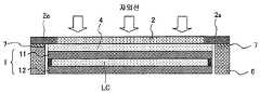
도 1 은, 제 1 의 본 발명의 일 실시형태의 액정 표시 장치의 패널 구성의 모식도이다. 이 액정 표시 장치는, 휴대전화나 휴대형 게임기 등에 사용되는 것으로서, 화상 표시를 실시하기 위한 액정 표시 패널 (1) 과, 그 표면을 보호하기 위한 보호 패널 (2) 을 구비하고, 이것들이 수지 경화물 (3) 을 개재하여 대향 배치되고, 또한 수지 경화물 (3) 의 표면 또는 배면 (背面) 의 대략 전체면과 각각 접착되고, 이로써, 시인성이나 내충격성을 개선하는 것으로 되어 있다.FIG. 1: is a schematic diagram of the panel structure of the liquid crystal display device of one Embodiment of 1st this invention. This liquid crystal display device is used for a mobile telephone, a portable game machine, etc., and is provided with the liquid
액정 표시 패널 (1) 에 있어서는, 1 쌍의 기판 (11, 12) 사이에 액정 재료를 끼워 넣어 액정층 (LC) 이 형성되어 있고, 이 액정층 (LC) 의 액정 재료의 배향을 제어함으로써 화상이 표시된다. 보다 구체적으로는, 1 쌍의 기판 (11, 12) 에는, 도시되지 않은 컬러 필터나 블랙 매트릭스, 화소 전극이나 대향 전극, 또는 구동 트랜지스터 등이 형성됨과 함께, 그 표면 및 이면 (裏面) 에는 편광판이 부착되고, 예를 들어 액티브 매트릭스 방식에 의해 각 화소가 구동되어 화상 표시된다. 또한, 1 쌍의 기판 (11, 12) 의 간극 (g) 이, 이른바 셀 갭이다.In the liquid
또, 이 화상 표시 장치에서는, 보호 패널 (2) 의 외주연부에 차광부 (2a) 가 형성되어 있다. 차광부 (2a) 를 포함한 보호 패널 (2) 의 외형 치수 (W2) 는 액정 표시 패널 (1) 의 외형 치수 (W1) 보다 약간 크고, 차광부 (2a) 가 액정 표시 패널 (1) 의 외주연의 내측으로부터 외측으로 돌출된 형태로 되어 있어, 액정 표시 패널 (1) 의 외주 부분으로부터의 광 누출을 차광부 (2a) 에 의해 확실하게 차광할 수 있도록 하고 있다.Moreover, in this image display apparatus, the
이와 같이 보호 패널 (2) 의 외주연부가 액정 표시 패널 (1) 의 외주연부로부터 돌출되어 있는 경우, 단지 이들 사이에 수지 조성물을 개재시키고, 그것을 경화시킴으로써 보호 패널 (2) 과 액정 표시 패널 (1) 을 부착시키면, 도 6 에 나타내는 바와 같이, 수지 조성물이 경화될 때 발생하는 내부 응력 (화살표 A) 이나, 보호 패널 (2) 이 환경 온도 변화에 의해 휠 때 외주 부분에 발생하는 외부 응력 (화살표 B) 에 의해, 수지 경화물 (3) 은, 특히 보호 패널 (2) 의 외주 부분에서 휘어올라, 액정 표시 패널 (1) 의 상면에 이들 응력이 가해지게 된다. 액정 표시 패널 (1) 에 이와 같은 응력이 가해지면, 액정 표시 패널 (1) 의 기판 (11, 12) 사이의 간극 (g) 이 예를 들어 중앙 부분과 주변 부분에서 나노 레벨로 변동되어, 표시 불균일이 발생될 가능성이 있다.Thus, when the outer periphery of the
이것에 대해, 본 실시형태에서는, 보호 패널 (2) 의 차광부 (2a) 의 상면 (즉, 액정 표시 패널 (1) 과 반대측의 보호 패널 (2) 의 면) 을 고정 지그 (5) 로 액정 표시 패널 (1) 측으로 누른 상태에서 수지 조성물을 경화시킴으로써, 경화시에 보호 패널 (2) 이 휘는 것을 방지하여, 액정 표시 패널 (1) 에 가능한 한 응력이 가해지지 않도록 하고 있다. 또한, 수지 조성물이 경화된 후에도, 도 1 에 나타내는 바와 같이, 고정 지그 (5) 로 계속해서 차광부 (2a) 의 상면을 누르도록 고정시킨다. 따라서, 본 실시형태에 의하면, 보호 패널 (2) 의 외주연부를 휘지 않는 상태로 유지할 수 있게 된다. 이하, 본 실시형태에서의 보호 패널의 부착 방법에 대해 상세히 서술한다.On the other hand, in this embodiment, the upper surface of the
도 2 는, 본 실시형태의 액정 표시 장치의 제조 방법에서, 보호 패널 (2) 의 부착 공정을 나타내는 것이다. 이 공정에서는, 먼저, 액정 표시 패널 (1) 과 보호 패널 (2) 사이에 수지 조성물 (4) 을 도포한다. 이 경우, 수지 조성물 (4) 을 액정 표시 패널 (1) 의 상면에 도포하고 나서 보호 패널 (2) 을 이 위에 겹쳐도 되고, 반대로 보호 패널 (2) 측에 수지 조성물 (4) 을 도포하고 나서, 이것을 반전시켜 액정 표시 패널 (1) 상에 겹쳐도 된다.FIG. 2: shows the attachment process of the
사용하는 수지 조성물 (4) 로는, 열 경화성, 광 경화성 (예를 들어 자외선 경화성) 등의 수지 조성물을 사용할 수 있다. 단, 최대한으로, 경화시의 고온 상태를 피한다는 점에서는, 자외선 경화성 등의 광 경화성 수지 조성물을 사용하는 것이 바람직하다. 본 실시형태에서도, 수지 조성물 (4) 로서 자외선 경화성의 수지 조성물을 사용하고 있다.As the resin composition (4) to be used, resin compositions, such as thermosetting and photocurable (for example, ultraviolet curable), can be used. However, from the point of avoiding the high temperature state at the time of hardening, it is preferable to use photocurable resin compositions, such as ultraviolet curability. Also in this embodiment, the ultraviolet curable resin composition is used as the resin composition (4).
또, 수지 조성물 (4) 로는, 경화 수축률이 바람직하게는 5 % 이하, 보다 바람직하게는 4.5 % 이하, 더욱 바람직하게는 4.0 % 이하, 가장 바람직하게는 0 ∼ 2 % 가 되도록 조제한 것을 사용한다. 이로써, 수지 조성물 (4) 이 경화될 때 수지 경화물 (3) 에 축적되는 내부 응력을 저감시킬 수 있어, 수지 경화물 (3) 과 액정 표시 패널 (1) 의 계면이나, 수지 경화물 (3) 과 보호 패널 (2) 의 계면에 변형이 발생되는 것을 방지할 수 있다.Moreover, as resin composition (4), what was prepared so that hardening shrinkage may become 5% or less, More preferably, it is 4.5% or less, More preferably, it is 4.0% or less, Most preferably, 0 to 2% is used. Thereby, when the
또한, 수지 조성물 (4) 로서는, 수지 경화물 (3) 의 저장 탄성률 (25 ℃) 이, 바람직하게는 1×10⁷ Pa 이하, 보다 바람직하게는 1×10³ Pa ∼ 1×10⁶ Pa 가 되도록 조제한 것을 사용한다. 이로써 수지 조성물 (4) 의 경화 후에 액정 표시 패널 (1) 에 가해지는 응력을 저감시킬 수 있다.Moreover, as the resin composition (4), the storage elastic modulus (25 degreeC) of the resin hardened | cured
또한, 상기 수지 조성물 (4) 이 경화될 때 수지 경화물 (3) 에 축적되는 내부 응력의 정도는, 수지 조성물을 평판 상에 적하시키고, 그것을 경화시켜 얻어지는 수지 경화물의 평균 표면 조도에 의해 평가할 수 있다. 예를 들어, 수지 조성물 2 ㎎ 을, 액정 표시 패널의 기판을 구성하는 유리판 또는 보호 패널을 구성하는 아크릴판 상에 적하시키고, 그것을 자외선 조사에 의해 90 % 이상의 경화율로 경화시켰을 때, 얻어지는 수지 경화물의 평균 표면 조도가 6.0 ㎚ 이하, 바람직하게는 5.0 ㎚ 이하, 보다 바람직하게는 1 ∼ 3 ㎚ 이면, 액정 표시 패널 (1) 이나 보호 패널 (2) 의 계면에 발생되는 변형을 실용상 무시할 수 있는 레벨로 할 수 있다. 또한 이 경우, 유리판이나 아크릴판의 평균 표면 조도는 통상적으로 1.0 ㎚ 이하이다. 따라서, 본 발명에서 사용하는 수지 조성물 (4) 도 액정 표시 패널의 기판을 구성하는 유리판 또는 아크릴판 상에 적하시킨 경우의 수지 경화물의 평균 표면 조도가 전술한 범위가 되는 것을 사용한다.In addition, when the said
수지 조성물 (4) 로서는, 광학 특성도 우수한 것이 필요하다. 예를 들어, 굴절률에 대해 언급하면, 수지 조성물 (4) 을 경화시킨 수지 경화물 (3) 의 굴절률이 액정 표시 패널 (1) 이나 보호 패널 (2) 의 굴절률과 동등한 것이 바람직하다. 예를 들어, 액정 표시 패널 (1) 의 기판 (11) 이 광학 유리로 형성되어 있는 경우, 그 굴절률 (nD) 은 1.49 ∼ 1.50 이고, 강화 유리로 형성되어 있는 경우에는 1.55 정도인 경우도 있고, 또, 보호 패널 (2) 이 아크릴 수지로 형성되어 있는 경우, 그 굴절률 (nD) 은 1.51 ∼ 1.52 가 되기 때문에, 수지 경화물 (3) 의 굴절률 (nD) 은 1.45 이상 1.55 이하인 것이 바람직하고, 1.51 이상 1.52 이하인 것이 보다 바람직하다.As the resin composition (4), what is excellent also in optical characteristics is required. For example, referring to the refractive index, it is preferable that the refractive index of the cured
또, 투명성에 관해서는, 수지 경화물 (3) 의 두께를 100 ㎛ 로 했을 때, 가시광 파장 영역의 광 투과율이 90 % 이상인 것이 바람직하다.Moreover, regarding transparency, when the thickness of the resin hardened | cured
이상과 같은 조건을 만족하는 수지 조성물로는, 예를 들어, 폴리우레탄아크릴레이트, 폴리이소프렌계 아크릴레이트 또는 그 에스테르화물, 테르펜계 수소 첨가 수지, 및 부타디엔 중합체 등에서 선택되는 1 종 이상의 폴리머와, 이소보르닐아크릴레이트, 디시클로펜테닐옥시에틸메타크릴레이트, 및 2-히드록시부틸메타크릴레이트 등에서 선택되는 1 종 이상의 아크릴레이트계 모노머와, 1-히드록시-시클로헥실-페닐-케톤 등의 광중합 개시제를 함유하는 수지 조성물 등을 들 수 있다. 이 경우, 경화 수축률이나 저장 탄성률, 광학 특성의 값이 전술한 범위 내에 포함되도록, 폴리머나 아크릴레이트계 모노머의 종류, 비율 등을 조정한다. 또한, 보호 패널 (2) 은, 액정 표시 패널 (1) 에 대한 자외선 보호 관점에서 자외선 영역의 광을 커트하는 기능이 부여되어 있는 경우가 많으므로, 광중합 개시제로는, 가시광 영역의 광으로도 경화시킬 수 있는 광중합 개시제 (예를 들어, 니혼 시이벨헤그너사 제조, 상품명 Speed Cure TPO 등) 를 병용하는 것이 바람직하다.Examples of the resin composition that satisfies the above conditions include at least one polymer selected from polyurethane acrylate, polyisoprene acrylate or esterified product thereof, terpene-based hydrogenated resin, butadiene polymer, and iso Photopolymerization, such as 1 or more acrylate-type monomers chosen from bornyl acrylate, dicyclopentenyl oxyethyl methacrylate, 2-hydroxybutyl methacrylate, and 1-hydroxy cyclohexyl phenyl- ketone The resin composition containing an initiator, etc. are mentioned. In this case, the kind, ratio, etc. of a polymer and an acrylate-type monomer are adjusted so that the value of a cure shrinkage rate, storage elastic modulus, and an optical characteristic may be contained in the range mentioned above. In addition, since the
수지 조성물 (4) 을 액정 표시 패널 (1) 혹은 보호 패널 (2) 에 도포하는 경우, 예를 들어 액정 표시 패널 (1) 주위에 스페이서를 형성하여 수지 조성물 (4) 을 도포한다. 물론, 스페이서를 생략할 수도 있다. 도포하는 수지 조성물 (4) 의 두께는 임의적이나, 수지 경화물 (3) 의 층두께가 50 ㎛ ∼ 200 ㎛ 정도가 되도록 도포하는 것이 바람직하다.When apply | coating the
수지 조성물 (4) 의 도포 후, 수지 조성물 (4) 을 개재하여 액정 표시 패널 (1) 과 보호 패널 (2) 을 겹친다. 여기에서, 보호 패널 (2) 은, 플라스틱제의 투명한 패널로서, 예를 들어, 폴리메틸메타크릴레이트 패널 등의 아크릴 수지 패널 등을 사용할 수 있다. 또, 본 실시형태에서는, 보호 패널 (2) 로서는, 그 외주연부에 광을 차광하는 차광부 (2a) 를 갖는 것을 사용한다. 차광부 (2a) 는, 예를 들어, 차광 테이프를 부착하거나, 차광 도료의 인쇄에 의해 형성된 것으로 할 수 있다.After application of the
보호 패널 (2) 의 외형 치수는 액정 표시 패널 (1) 의 외형 치수보다 크므로, 이들을 겹치면, 보호 패널 (2) 의 외주연부가 액정 표시 패널 (1) 의 외주연부로부터 돌출하는 형태가 되고, 이 상태에서 단순히 자외선을 조사하여 수지 조성물 (4) 을 경화시켜 보호 패널 (2) 을 접합하면, 보호 패널 (2) 이 휘어지는 문제가 발생된다. 그래서, 본 실시형태에서는, 도 2 에 나타내는 바와 같이, 고정 지그 (5) 를 사용하여 보호 패널 (2) 의 외주연 부분을 보호 패널 (2) 의 상면으로부터 누르도록 고정시킨 상태에서 수지 조성물 (4) 을 경화시킨다.Since the external dimension of the
보다 구체적으로는, 고정 지그 (5) 는, 예를 들어 액정 표시 패널 (1) 이나 보호 패널 (2) 을 내부에 수용할 수 있는 프레임 형상인 것으로서, 상단부가 절곡되어 차양 형상의 누름부 (5a) 로 되어 있는 것을 사용할 수 있다. 이 누름부 (5a) 에 의해 차광부 (2a) 로 되어 있는 보호 패널 (2) 의 외주연부의 상면을 누르고, 자외선 조사에 의해 수지 조성물 (4) 을 경화시킨다. 이로써, 보호 패널 (2) 이 휘는 것이 교정된 상태에서 수지 조성물 (4) 을 경화시키므로, 보호 패널 (2) 의 평탄성이 유지된다. 또, 자외선 조사에 의해 수지 조성물을 경화시키는 경우에도, 실제로는, 보호 패널 (2) 이 열선에 노출되게 되는데, 차광부 (2a) 를 누름부 (5a) 로 고정시켜 두면, 보호 패널 (2) 이 고온이 되어도 휨이 확대되지 않는다.More specifically, the fixing
또한, 고정 지그 (5) 는, 수지 조성물 (4) 을 경화시킬 때에만 사용하는 전용 지그여도 되는데, 보호 패널 (2) 이 접착된 액정 표시 패널 (1) 을 수용하는 케이스를 유용 (流用) 할 수도 있다. 액정 표시 패널 (1) 이 삽입되는 액정 표시 장치의 케이스에 상기 차양 형상의 누름부 (5a) 를 형성해 두면, 케이스에 액정 표시 패널 (1) 등을 삽입함으로써 전술한 누름 상태가 얻어진다. 그리고, 이 경우, 케이스를 그대로 사용할 수 있고, 수지 조성물 (4) 의 경화 완료와 동시에 액정 표시 패널 (1) 의 삽입도 완료되게 된다. 즉, 도 2 의 상태가 그대로 액정 표시 장치의 구조가 된다. 또한, 이 경우, 보호 패널 (2) 의 상면이 수지 조성물 (4) 의 경화 후에도 계속 케이스로 지지 고정되게 되어, 보호 패널 (2) 이 경시적으로 휘는 것도 방지할 수 있다.In addition, although the fixed
이상에 의해 제조된 액정 표시 장치는, 보호 패널 (2) 이 휘는 것이 확실하게 억제되어, 표시 불균일 등이 발생되지 않는 신뢰성 높은 액정 표시 장치가 된다. 또, 보호 패널 (2) 과 액정 표시 패널 (1) 사이에 수지 경화물 (3) 이 충전된 상태로 되어 있으므로, 옥외에서의 시인성도 충분히 확보할 수 있고, 내충격성도 확보할 수 있다.The liquid crystal display device manufactured by the above is reliably suppressed by the
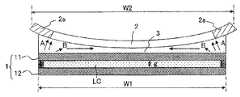
도 3 은, 제 1 의 본 발명의 상이한 실시형태인 화상 표시 장치의 패널 구성의 모식도이다. 이 화상 표시 장치에서는, 플라스틱에 의해 형성된 보호 패널 (2) 의 외주연부의 하면, 즉, 보호 패널 (2) 의 화상 표시 패널 (1) 측의 면이 고정 지그 (6) 의 상단면에 접착 고정되어 있는 점이 도 1 의 화상 표시 장치와 상이하고, 그 밖에는 동일하게 형성되어 있다.FIG. 3: is a schematic diagram of the panel structure of the image display apparatus which is different embodiment of 1st this invention. In this image display apparatus, the lower surface of the outer periphery of the
이 실시형태에서의 보호 패널 (2) 의 접착 방법은, 전술한 것과 동일하게 수지 조성물 (4) 을 도포한 후, 수지 조성물 (4) 을 개재하여 액정 표시 패널 (1) 과 보호 패널 (2) 을 겹치는데, 이 때, 도 4 에 나타내는 바와 같이, 보호 패널 (2) 과 거의 동일한 외형 치수를 갖는 프레임 형상의 고정 지그 (6) 를 사용하고, 이 고정 지그 (6) 의 상단면에서 보호 패널 (2) 의 외주연부를 고정시킨다. 예를 들어, 고정 지그 (6) 의 상단면에 접착 테이프 (7) 를 부착해 두고, 보호 패널 (2) 을 접착 고정시킨다. 이 상태에서 자외선을 조사하여, 수지 조성물 (4) 을 경화시키면, 도 1 의 실시형태의 경우와 동일하게, 보호 패널 (2) 이 휘는 것이 확실하게 억제된다.In the adhesion method of the
본 실시형태에서도, 고정 지그 (6) 는, 수지 조성물 (4) 을 경화시킬 때에만 사용하는 전용 지그여도 되고, 액정 표시 패널 (1) 을 수용하는 케이스를 유용해도 된다. 후자의 경우, 도 3 의 상태가 그대로 액정 표시 장치의 구조가 된다.Also in this embodiment, the fixed
도 5 는, 제 2 의 본 발명의 일 실시형태의 액정 표시 장치의 패널 구성 제조 방법의 모식도이다. 실시형태에서는, 보호 패널 (2) 의 외형 치수를 액정 표시 패널 (1) 의 외형 치수와 대략 동등하게 하고, 또한, 이들 외형 치수와 이들 케이스 (8) 의 내측 치수를 대략 동등하게 하고, 보호 패널 (2) 의 대략 전체면에 수지 조성물 (4) 이 접한 상태에서 당해 수지 조성물 (4) 을 경화시키는 점을 특징 사항으로 하는 실시형태이다. 또한, 본 실시형태에서도, 수지 조성물 (4) 을 도포하기까지에 대해서는, 앞서의 제 1 의 본 발명의 실시형태의 경우와 동일하므로, 여기에서는 그 설명은 생략한다.It is a schematic diagram of the panel structure manufacturing method of the liquid crystal display device of one Embodiment of 2nd this invention. In embodiment, the external dimension of the
전술한 바와 같이, 수지 조성물 (4) 을 액정 표시 패널 (1) 상에 도포한 후, 그 위에 보호 패널 (2) 을 겹쳤는데, 이 때, 도 5 에 나타내는 바와 같이, 보호 패널 (2) 의 외형 치수를 액정 표시 패널 (1) 의 외형 치수와 거의 동등하게 한다. 이로써, 보호 패널 (2) 의 전체면이 수지 조성물 (4) 과 접하게 되어, 이른바 휘는 영역이 없는 상태가 된다. 이 상태에서, 케이스 (8) 내에 수용한다. 여기에서, 케이스 (8) 의 내측 치수는, 보호 패널 (2) 이나 액정 표시 패널 (1) 의 외형 치수와 대략 동등하게 하고, 액정 표시 패널 (1) 상에 중첩된 보호 패널 (2) 을 정확하게 케이스 (8) 내에 끼워넣도록 한다. 이 상태에서, 자외선을 조사하여 수지 조성물 (4) 을 경화시키면, 보호 패널 (2) 이 휘는 것이 간편하게 또한 확실하게 억제된다. 휨이 현저해지는 보호 패널 (2) 의 돌출 부분이 없고, 또한 보호 패널 (2) 이 휘어오르는 것이, 그 측면에 맞닿아 있는 케이스 (8) 에 의해 억제되기 때문이다. 또한, 본 실시형태의 경우에는, 차광부를 별도 형성할 필요가 있다.As above-mentioned, after apply | coating the
이상, 본 발명의 실시형태에 대해 설명하였는데, 본 발명이 전술한 실시형태에 한정되지 않는 것은 말할 필요도 없고, 본 발명의 요지를 일탈하지 않는 범위에서 여러 가지 변경이 가능하다. 예를 들어, 보호 패널의 외주연부에서 차광부를 생략해도 된다. 또, 전술한 실시형태는 모두 본 발명을 액정 표시 장치에 적용한 실시형태이나, 본 발명은 액정 표시 장치 이외에도 적용할 수 있는데, 예를 들어 유기 EL 표시 장치나 플라스마 디스플레이 등에도 적용할 수 있다.As mentioned above, although embodiment of this invention was described, it cannot be overemphasized that this invention is not limited to embodiment mentioned above, A various change is possible in the range which does not deviate from the summary of this invention. For example, the light shielding portion may be omitted from the outer peripheral edge of the protective panel. Moreover, all the above-mentioned embodiment is embodiment which applied this invention to the liquid crystal display device, but this invention can be applied also other than a liquid crystal display device, For example, it can be applied also to an organic electroluminescence display, a plasma display, etc.
실시예Example
다음으로, 본 발명의 구체적인 실시예에 대해, 실험 결과를 기초로 설명한다.Next, specific examples of the present invention will be described based on experimental results.
(실시예 1)(Example 1)
도 2 에 나타낸 방법에 따라 보호 패널을 액정 표시 패널에 부착하여, 액정 표시 장치를 제조하였다. 사용한 보호 패널은, 폴리메틸메타크릴레이트 (PMMA) 에 의해 형성된 투명 플라스틱 패널이다. 고정 지그로서는, 액정 표시 패널을 수용하는 케이스를 이용하고, 이 케이스에 차양 형상의 누름부를 형성함으로써 보호 패널의 외주연부에 형성되어 있는 차광부의 상면을 눌러 고정시켰다.According to the method shown in FIG. 2, a protective panel was attached to the liquid crystal display panel, and the liquid crystal display device was manufactured. The used protective panel is a transparent plastic panel formed of polymethyl methacrylate (PMMA). As the fixing jig, a case accommodating the liquid crystal display panel was used, and the upper surface of the light shielding portion formed on the outer periphery of the protective panel was pressed and fixed by forming a shading pressing portion on the case.
액정 표시 패널과 보호 패널 사이에 개재시키는 수지 조성물로는, 폴리이소프렌 중합물의 무수 말레산 부가물과 2-히드록시에틸메타크릴레이트의 에스테르화물 70 중량부, 디시클로펜테닐옥시에틸메타크릴레이트 30 중량부, 2-히드록시부틸메타크릴레이트 10 중량부, 테르펜계 수소 첨가 수지 30 중량부, 부타디엔 중합체 140 중량부, 광중합 개시제 4 중량부, 가시광 영역용 광중합 개시제 0.5 중량부를 혼련기로 혼련하여 조제하였다.As the resin composition interposed between the liquid crystal display panel and the protective panel, 70 parts by weight of an esterified product of maleic anhydride adduct of a polyisoprene polymer and 2-hydroxyethyl methacrylate and dicyclopentenyloxyethyl methacrylate 30 Parts by weight, 10 parts by weight of 2-hydroxybutyl methacrylate, 30 parts by weight of terpene-based hydrogenated resin, 140 parts by weight of butadiene polymer, 4 parts by weight of photopolymerization initiator, and 0.5 parts by weight of photopolymerization initiator for visible region were kneaded with a kneader. .
이 수지 조성물의 경화 수축률은 1.8 %, 이 수지 조성물을 경화시킨 수지 경화물의 저장 탄성률 (25 ℃) 은 1×10⁴ Pa 였다. 또, 수지 조성물 2 ㎎ 을 액정 셀용 유리판 상에 적하시키고, 그것을 자외선 조사에 의해 90 % 이상의 경화율로 경화시켰을 때 얻어지는 수지 경화물의 평균 표면 조도는 2.7 ㎚ 였다. 또한, 상기 수지 조성물에 의해 두께 100 ㎛ 의 수지 경화물을 형성하고, 자외 가시 분광 광도계 (니혼 분광사 제조, 상품명 V-560) 에 의해 가시광 영역의 투과율을 측정한 결과, 90 % 이상이었다.The cure shrinkage rate of this resin composition was 1.8%, and the storage elastic modulus (25 degreeC) of the cured resin material which hardened this resin composition was 1 * 10 <4> Pa. Moreover, the average surface roughness of the resin hardened | cured material obtained when 2 mg of resin compositions were dripped on the glass plate for liquid crystal cells, and it hardened at 90% or more of curing rates by ultraviolet irradiation was 2.7 nm. Moreover, the resin cured material of thickness 100micrometer was formed with the said resin composition, and when the transmittance | permeability of visible region was measured by the ultraviolet-visible spectrophotometer (The Nihon spectroscopy company make, brand name V-560), it was 90% or more.
또한, 저장 탄성률은 점탄성 측정 장치 (세이코 인스트루먼트사 제조, 상품명 DMS6100) 를 사용하여, 측정 주파수 1 Hz 로 탄성률 (Pa) (25 ℃) 을 측정하였다.In addition, the storage elastic modulus measured the elasticity modulus (Pa) (25 degreeC) by the measurement frequency of 1 Hz using a viscoelasticity measuring instrument (the Seiko Instruments company make, brand name DMS6100).
경화 수축률은, 경화 전의 수지액과 경화 후의 고체의 비중을 전자 비중계 (MIRAGE 사 제조, 상품명 SD-120L) 를 사용하여 측정하고, 양자의 비중차로부터 다음 식에 의해 산출하였다.The cure shrinkage rate measured the specific gravity of the resin liquid before hardening, and the solid after hardening using the electronic hydrometer (MIRAGE make, brand name SD-120L), and was computed by the following formula from the specific gravity difference of both.
경화 수축률 (%)=(경화물 비중-수지액 비중)/경화물 비중×100Hardening shrinkage rate (%) = (harden specific gravity-resin specific gravity) / hardened specific gravity x 100
평균 표면 조도는, 유리판 표면의 소정 영역 (2.93 mm×2.20 mm) 의 변형 (Ra : 평균 표면 조도) 을, Zygo 사 제조의 3 차원 비접촉 표면 조도 측정계로 측정하여 얻었다.The average surface roughness measured and obtained the deformation | transformation (Ra: average surface roughness) of the predetermined | prescribed area | region (2.93 mm x 2.20 mm) of the glass plate surface by the 3-dimensional non-contact surface roughness measuring instrument by Zygo.
본 실시예에 의해, 보호 패널이 휘는 것이 거의 발생되지 않아 표시 불균일이 없어, 옥외에서의 시인성이나 내충격성이 우수한 액정 표시 장치를 얻을 수 있었다.According to this embodiment, the protective panel hardly bends, there is no display unevenness, and a liquid crystal display device excellent in visibility and impact resistance outdoors can be obtained.
(실시예 2)(Example 2)
액정 표시 패널과 보호 패널 사이에 개재시키는 수지 조성물을 다음과 같이 변경하고, 그 밖에는 실시예 1 과 동일하게 하여 액정 표시 장치를 제조하였다. 본 실시예에서도, 보호 패널이 휘는 것이 거의 발생되지 않아 표시 불균일이 없어, 옥외에서의 시인성이나 내충격성이 우수한 액정 표시 장치를 얻을 수 있었다.The resin composition interposed between the liquid crystal display panel and the protective panel was changed as follows, and else the liquid crystal display device was manufactured in the same manner as in Example 1. Also in this embodiment, almost no bending of the protection panel occurred, there was no display unevenness, and a liquid crystal display device excellent in visibility and impact resistance outdoors was obtained.
즉, 본 실시예에서 수지 조성물은, 폴리이소프렌 중합물의 무수 말레산 부가물과 2-히드록시에틸메타크릴레이트의 에스테르화물 100 중량부, 디시클로펜테닐옥시에틸메타크릴레이트 30 중량부, 2-히드록시부틸메타크릴레이트 10 중량부, 테르펜계 수소 첨가 수지 30 중량부, 부타디엔 중합체 210 중량부, 광중합 개시제 7 중량부, 가시광 영역용 광중합 개시제 1.5 중량부를 혼련기로 혼련하여 조제하였다.That is, in this embodiment, the resin composition comprises 100 parts by weight of an esterified product of 2-hydroxyethyl methacrylate and maleic anhydride adduct of a polyisoprene polymer, 30 parts by weight of dicyclopentenyloxyethyl methacrylate, and 2- 10 parts by weight of hydroxybutyl methacrylate, 30 parts by weight of terpene-based hydrogenated resin, 210 parts by weight of butadiene polymer, 7 parts by weight of photopolymerization initiator, and 1.5 parts by weight of photopolymerization initiator for visible light region were kneaded with a kneader.
이 수지 조성물의 경화 수축률은 1.0 %, 이 수지 조성물을 경화시킨 수지 경화물의 저장 탄성률 (25 ℃) 은 4×10³ Pa 였다. 또, 수지 조성물 2 ㎎ 을 액정셀용 유리판 상에 적하시키고, 그것을 자외선 조사에 의해 90 % 이상의 경화율로 경화시켰을 때 얻어지는 수지 경화물의 평균 표면 조도는 1.5 ㎚ 였다. 또한, 이 수지 조성물로 형성한 두께 100 ㎛ 의 수지 경화물의 자외 가시 분광 광도계 (니혼 분광사 제조, 상품명 V-560) 에 의한 가시광 영역의 투과율은 90 % 이상이었다.The cure shrinkage rate of this resin composition was 1.0%, and the storage elastic modulus (25 degreeC) of the cured resin material which hardened this resin composition was 4 * 10 <3> Pa. Moreover, the average surface roughness of the resin hardened | cured material obtained when 2 mg of resin compositions were dripped on the glass plate for liquid crystal cells, and it hardened at 90% or more of curing rates by ultraviolet irradiation was 1.5 nm. In addition, the transmittance | permeability of the visible light area | region by the ultraviolet-visible spectrophotometer (The Nihon spectroscopy company make, brand name V-560) of the resin hardened | cured material of thickness 100micrometer formed from this resin composition was 90% or more.
(실시예 3)(Example 3)
액정 표시 패널과 보호 패널 사이에 개재시키는 수지 조성물을 다음과 같이 변경하고, 그 밖에는 실시예 1 과 동일하게 하여 액정 표시 장치를 제조하였다. 본 실시예에서도, 보호 패널이 휘는 것이 거의 발생되지 않아 표시 불균일이 없어, 옥외에서의 시인성이나 내충격성이 우수한 액정 표시 장치를 얻을 수 있었다.The resin composition interposed between the liquid crystal display panel and the protective panel was changed as follows, and else the liquid crystal display device was manufactured in the same manner as in Example 1. Also in this embodiment, almost no bending of the protection panel occurred, there was no display unevenness, and a liquid crystal display device excellent in visibility and impact resistance outdoors was obtained.
즉, 본 실시예에서 수지 조성물은, 폴리이소프렌 중합물의 무수 말레산 부가물과 2-히드록시에틸메타크릴레이트의 에스테르화물 (쿠라레사 제조, 상품명 UC-203) 70 중량부, 디시클로펜테닐옥시에틸메타크릴레이트 (히타치 화성 공업사 제조, 상품명 FA512M) 30 중량부, 2-히드록시부틸메타크릴레이트 (쿄에이샤 화학사 제조, 상품명 라이트 에스테르 HOB) 10 중량부, 테르펜계 수소 첨가 수지 (야스하라 케미컬사 제조, 상품명 클리어론 P-85) 30 중량부, 부타디엔 중합체 (니혼 제온사 제조, 상품명 Polyoil 110) 35 중량부, 광중합 개시제 (치바 스페셜리티 케미컬즈사 제조, 상품명 이르가큐어 184D) 5 중량부, 가시광 영역용 광중합 개시제 (니혼 시이벨헤그너사 제조, 상품명 Speed Cure TPO) 2 중량부를 혼련기로 혼련하여 조제하였다.That is, in this embodiment, the resin composition is 70 parts by weight of esterified product of maleic anhydride adduct of polyisoprene polymer and 2-hydroxyethyl methacrylate (Kuraraya, trade name UC-203), dicyclopentenyloxy 30 parts by weight of ethyl methacrylate (manufactured by Hitachi Chemical Co., Ltd., FA512M), 10 parts by weight of 2-hydroxybutyl methacrylate (manufactured by Kyoeisha Chemical Company, trade name light ester HOB), terpene-based hydrogenated resin (Yashara Chemical) 30 parts by weight of manufactured, trade name Clearon P-85), 35 parts by weight of butadiene polymer (manufactured by Nippon Zeon, trade name Polyoil 110), 5 parts by weight of a photopolymerization initiator (Ciba Specialty Chemicals, trade name Irgacure 184D) 2 parts by weight of an area photopolymerization initiator (Nihon Siebel Hegner, trade name Speed Cure TPO) were kneaded with a kneader to prepare.
이 수지 조성물의 경화 수축률은 3.8 %, 이 수지 조성물을 경화시킨 수지 경화물의 저장 탄성률 (25 ℃) 은 4×10⁵ Pa 였다. 또, 수지 조성물 2 ㎎ 을 액정셀용 유리판 상에 적하시키고, 그것을 자외선 조사에 의해 90 % 이상의 경화율로 경화시켰을 때 얻어지는 수지 경화물의 평균 표면 조도는 5.0 ㎚ 였다. 또한, 이 수지 조성물로 형성한 두께 100 ㎛ 의 수지 경화물의 자외 가시 분광 광도계 (니혼 분광사 제조, 상품명 V-560) 에 의한 가시광 영역의 투과율은 90 % 이상이었다.The cure shrinkage rate of this resin composition was 3.8%, and the storage elastic modulus (25 degreeC) of the cured resin material which hardened this resin composition was 4 * 10 <5> Pa. Moreover, the average surface roughness of the resin hardened | cured material obtained when 2 mg of resin compositions were dripped on the glass plate for liquid crystal cells, and it hardened at 90% or more of curing rates by ultraviolet irradiation was 5.0 nm. In addition, the transmittance | permeability of the visible light area | region by the ultraviolet-visible spectrophotometer (The Nihon spectroscopy company make, brand name V-560) of the resin hardened | cured material of thickness 100micrometer formed from this resin composition was 90% or more.
(실시예 4)(Example 4)
실시예 1 과 동일한 보호 패널을 사용하고, 도 3 에 나타낸 방법에 따라 보호 패널을 액정 표시 패널에 부착시켜 액정 표시 장치를 제조하였다. 사용한 수지 조성물도 실시예 1 과 동일하게 하였다.Using the same protective panel as in Example 1, the protective panel was attached to the liquid crystal display panel according to the method shown in FIG. 3 to manufacture a liquid crystal display device. The used resin composition was also performed similarly to Example 1.
본 실시예에서도, 보호 패널이 휘는 것이 거의 발생되지 않아 표시 불균일이 없어, 옥외에서의 시인성이나 내충격성이 우수한 액정 표시 장치를 얻을 수 있었다.Also in this embodiment, almost no bending of the protection panel occurred, there was no display unevenness, and a liquid crystal display device excellent in visibility and impact resistance outdoors was obtained.
(실시예 5)(Example 5)
실시예 1 과 동일한 보호 패널을 사용하고, 도 3 에 나타낸 방법에 따라 보호 패널을 액정 표시 패널에 부착시켜 액정 표시 장치를 제조하였다. 사용한 수지 조성물은 실시예 2 와 동일하게 하였다.Using the same protective panel as in Example 1, the protective panel was attached to the liquid crystal display panel according to the method shown in FIG. 3 to manufacture a liquid crystal display device. The used resin composition was carried out similarly to Example 2.
본 실시예에서도, 보호 패널이 휘는 것이 거의 발생되지 않아 표시 불균일이 없어, 옥외에서의 시인성이나 내충격성이 우수한 액정 표시 장치를 얻을 수 있었다.Also in this embodiment, almost no bending of the protection panel occurred, there was no display unevenness, and a liquid crystal display device excellent in visibility and impact resistance outdoors was obtained.
(실시예 6)(Example 6)
실시예 1 과 동일한 보호 패널을 사용하고, 도 3 에 나타낸 방법에 따라 보호 패널을 액정 표시 패널에 부착시켜 액정 표시 장치를 제조하였다. 사용한 수지 조성물은 실시예 3 과 동일하게 하였다.Using the same protective panel as in Example 1, the protective panel was attached to the liquid crystal display panel according to the method shown in FIG. 3 to manufacture a liquid crystal display device. The used resin composition was carried out similarly to Example 3.
본 실시예에서도, 보호 패널이 휘는 것이 거의 발생되지 않아 표시 불균일이 없어, 옥외에서의 시인성이나 내충격성이 우수한 액정 표시 장치를 얻을 수 있었다.Also in this embodiment, almost no bending of the protection panel occurred, there was no display unevenness, and a liquid crystal display device excellent in visibility and impact resistance outdoors was obtained.
(실시예 7)(Example 7)
실시예 1 과 동일한 보호 패널을 사용하고, 도 5 에 나타낸 방법에 따라 보호 패널 부착시의 수지 경화를 실시하여 액정 표시 장치를 제조하였다. 사용한 수지 조성물은 실시예 1 과 동일하다. 본 실시예에서도, 보호 패널이 휘는 것이 거의 발생되지 않아 표시 불균일이 없어, 옥외에서의 시인성이나 내충격성이 우수한 액정 표시 장치를 얻을 수 있었다.Using the same protective panel as in Example 1, resin curing at the time of attaching the protective panel was carried out according to the method shown in FIG. 5 to manufacture a liquid crystal display device. The used resin composition is the same as that of Example 1. Also in this embodiment, almost no bending of the protection panel occurred, there was no display unevenness, and a liquid crystal display device excellent in visibility and impact resistance outdoors was obtained.
(실시예 8)(Example 8)
실시예 1 과 동일한 보호 패널을 사용하고, 도 5 에 나타낸 방법에 따라 보호 패널 부착시의 수지 경화를 실시하여 액정 표시 장치를 제조하였다. 사용한 수지 조성물은 실시예 2 와 동일하다. 본 실시예에서도, 보호 패널이 휘는 것이 거의 발생되지 않아 표시 불균일이 없어, 옥외에서의 시인성이나 내충격성이 우수한 액정 표시 장치를 얻을 수 있었다.Using the same protective panel as in Example 1, resin curing at the time of attaching the protective panel was carried out according to the method shown in FIG. 5 to manufacture a liquid crystal display device. The used resin composition is the same as that of Example 2. Also in this embodiment, almost no bending of the protection panel occurred, there was no display unevenness, and a liquid crystal display device excellent in visibility and impact resistance outdoors was obtained.
(실시예 9)(Example 9)
실시예 1 과 동일한 보호 패널을 사용하고, 도 5 에 나타낸 방법에 따라 보호 패널 부착시의 수지 경화를 실시하여 액정 표시 장치를 제조하였다. 사용한 수지 조성물은 실시예 3 과 동일하다. 본 실시예에서도, 보호 패널이 휘는 것이 거의 발생되지 않아 표시 불균일이 없어, 옥외에서의 시인성이나 내충격성이 우수한 액정 표시 장치를 얻을 수 있었다.Using the same protective panel as in Example 1, resin curing at the time of attaching the protective panel was carried out according to the method shown in FIG. 5 to manufacture a liquid crystal display device. The used resin composition is the same as that of Example 3. Also in this embodiment, almost no bending of the protection panel occurred, there was no display unevenness, and a liquid crystal display device excellent in visibility and impact resistance outdoors was obtained.
1 액정 표시 패널
2 보호 패널
2a 차광부
3 수지 경화물
4 수지 조성물
5, 6 고정 지그
5a 누름부
7 접착 테이프
8 케이스1 liquid crystal display panel
2 protection panel
2a shading
3 resin cured product
4 resin composition
5, 6 fixed jig
5a press
7 adhesive tape
8 cases
Claims (1)
Translated fromKoreanApplications Claiming Priority (7)
| Application Number | Priority Date | Filing Date | Title |
|---|---|---|---|
| JPJP-P-2007-186360 | 2007-07-17 | ||
| JP2007186360 | 2007-07-17 | ||
| JP2008005027 | 2008-01-11 | ||
| JPJP-P-2008-005027 | 2008-01-11 | ||
| JP2008102051 | 2008-04-10 | ||
| JPJP-P-2008-102051 | 2008-04-10 | ||
| PCT/JP2008/062866WO2009011373A1 (en) | 2007-07-17 | 2008-07-16 | Image display device and method for manufacturing the same |
Related Parent Applications (1)
| Application Number | Title | Priority Date | Filing Date |
|---|---|---|---|
| KR1020127007367ADivisionKR101343659B1 (en) | 2007-07-17 | 2008-07-16 | Image display device and method for manufacturing the same |
Publications (1)
| Publication Number | Publication Date |
|---|---|
| KR20130122006Atrue KR20130122006A (en) | 2013-11-06 |
Family
ID=40259705
Family Applications (4)
| Application Number | Title | Priority Date | Filing Date |
|---|---|---|---|
| KR1020107000882AActiveKR101326463B1 (en) | 2007-07-17 | 2008-07-16 | Image display device and method for manufacturing the same |
| KR1020127007367AActiveKR101343659B1 (en) | 2007-07-17 | 2008-07-16 | Image display device and method for manufacturing the same |
| KR1020137026158ACeasedKR20130122006A (en) | 2007-07-17 | 2008-07-16 | Image display device and method for manufacturing the same |
| KR1020137020373ACeasedKR20130095854A (en) | 2007-07-17 | 2008-07-16 | Image display device and method for manufacturing the same |
Family Applications Before (2)
| Application Number | Title | Priority Date | Filing Date |
|---|---|---|---|
| KR1020107000882AActiveKR101326463B1 (en) | 2007-07-17 | 2008-07-16 | Image display device and method for manufacturing the same |
| KR1020127007367AActiveKR101343659B1 (en) | 2007-07-17 | 2008-07-16 | Image display device and method for manufacturing the same |
Family Applications After (1)
| Application Number | Title | Priority Date | Filing Date |
|---|---|---|---|
| KR1020137020373ACeasedKR20130095854A (en) | 2007-07-17 | 2008-07-16 | Image display device and method for manufacturing the same |
Country Status (7)
| Country | Link |
|---|---|
| US (3) | US20100134713A1 (en) |
| EP (3) | EP2180367B1 (en) |
| JP (1) | JP5206953B2 (en) |
| KR (4) | KR101326463B1 (en) |
| CN (4) | CN102253514B (en) |
| TW (1) | TW200914924A (en) |
| WO (1) | WO2009011373A1 (en) |
Families Citing this family (32)
| Publication number | Priority date | Publication date | Assignee | Title |
|---|---|---|---|---|
| WO2010044291A1 (en)* | 2008-10-17 | 2010-04-22 | シャープ株式会社 | Display device and method for manufacturing the same |
| JP2011227369A (en)* | 2010-04-22 | 2011-11-10 | Hitachi Displays Ltd | Image display device and manufacturing method of the same |
| KR101146994B1 (en)* | 2010-06-10 | 2012-05-22 | 삼성모바일디스플레이주식회사 | A display apparatus and a method for manufacturing the same |
| CN102985960B (en)* | 2010-06-21 | 2015-04-29 | 夏普株式会社 | Display panel equipped with front plate, display device, and resin composition |
| WO2012002019A1 (en)* | 2010-06-29 | 2012-01-05 | シャープ株式会社 | Display device |
| JP5750848B2 (en) | 2010-08-26 | 2015-07-22 | 住友化学株式会社 | Optical member for image display device |
| KR101211371B1 (en)* | 2010-09-16 | 2012-12-13 | 주식회사 토비스 | Method for manufacturing display panel with curved shape |
| WO2012060324A1 (en)* | 2010-11-05 | 2012-05-10 | コニカミノルタオプト株式会社 | Method for manufacturing liquid crystal display device provided with front plate, and liquid crystal display device provided with front plate |
| JPWO2012081708A1 (en)* | 2010-12-16 | 2014-05-22 | 日立化成株式会社 | Photocurable resin composition, image display device, and method for producing the same |
| JP2012145751A (en)* | 2011-01-12 | 2012-08-02 | Nippon Shokubai Co Ltd | Ultraviolet curable resin composition for optical use, hardened material, and display device |
| JP5685270B2 (en) | 2011-01-18 | 2015-03-18 | シャープ株式会社 | Display panel with flat plate and method for manufacturing display panel with flat plate |
| JP2012172064A (en) | 2011-02-22 | 2012-09-10 | Nitto Denko Corp | Ultraviolet-curable optical resin adhesive composition |
| CN104558441A (en)* | 2011-03-11 | 2015-04-29 | 日立化成株式会社 | Liquid curable resin composition, production method for image display device using same, and image display device |
| JP5892736B2 (en)* | 2011-05-24 | 2016-03-23 | ソニー株式会社 | Display device |
| MY170060A (en) | 2011-10-21 | 2019-07-02 | Nippon Kayaku Kk | Method for producing optical member and use of ultraviolet ray cured resin composition for same |
| TWI557204B (en) | 2012-02-17 | 2016-11-11 | Three Bond Fine Chemical Co Ltd | Optically hardened sheet-like adhesive composition |
| TWI472836B (en)* | 2012-09-25 | 2015-02-11 | Au Optronics Corp | Display module |
| DE102012224352A1 (en) | 2012-12-21 | 2014-06-26 | Continental Automotive Gmbh | Electro-optical display with a transparent cover |
| JP6609093B2 (en) | 2013-05-13 | 2019-11-20 | 日東電工株式会社 | Hard coat film, polarizing plate and image display device |
| KR102279707B1 (en) | 2013-12-18 | 2021-07-22 | 삼성디스플레이 주식회사 | Display apparatus |
| KR102171307B1 (en)* | 2013-12-19 | 2020-10-28 | 삼성전자주식회사 | Three dimensional display apparatus and manufacturing method for the same |
| US11097514B2 (en)* | 2014-05-12 | 2021-08-24 | Corning Incorporated | Method of improving optical quality of curved glass structures |
| JP2015225291A (en)* | 2014-05-29 | 2015-12-14 | 日本精機株式会社 | Display device |
| KR20160124310A (en) | 2015-04-16 | 2016-10-27 | 삼성디스플레이 주식회사 | Display module |
| KR20170028164A (en)* | 2015-09-03 | 2017-03-13 | 엘지전자 주식회사 | Mobile terminal |
| US10564678B2 (en)* | 2015-10-26 | 2020-02-18 | Motorola Mobility Llc | Display screen and display lens of electronic device |
| WO2017096529A1 (en)* | 2015-12-08 | 2017-06-15 | 华为技术有限公司 | Touch display screen |
| US9946104B2 (en) | 2015-12-28 | 2018-04-17 | Japan Display Inc. | Display device and method of manufacturing the same |
| JP7038477B2 (en)* | 2017-02-27 | 2022-03-18 | デクセリアルズ株式会社 | Image display device and its manufacturing method |
| CN110574095A (en)* | 2017-04-19 | 2019-12-13 | Agc株式会社 | Cover member and display device |
| US12142621B2 (en)* | 2019-03-08 | 2024-11-12 | Dexerials Corporation | Method of manufacturing connection structure, connection structure, film structure, and method of manufacturing film structure |
| CN113474872A (en)* | 2019-03-08 | 2021-10-01 | 迪睿合株式会社 | Method for manufacturing connection structure, film structure, and method for manufacturing film structure |
Family Cites Families (146)
| Publication number | Priority date | Publication date | Assignee | Title |
|---|---|---|---|---|
| US4679918A (en)* | 1984-10-23 | 1987-07-14 | Ace Ronald S | Ophthalmic glass/plastic laminated lens having photochromic characteristics and assembly thereof |
| JPH01300246A (en) | 1988-05-28 | 1989-12-04 | Nippon Paint Co Ltd | Photosensitive resin composition for flexography |
| US5126620A (en)* | 1988-12-19 | 1992-06-30 | Mitsubishi Denki Kabushiki Kaisha | Display element |
| JPH02165188A (en) | 1988-12-19 | 1990-06-26 | Mitsubishi Electric Corp | display element |
| JPH03204616A (en) | 1990-01-08 | 1991-09-06 | Hitachi Ltd | lcd display |
| JPH0675701A (en) | 1992-08-25 | 1994-03-18 | Nitto Denko Corp | Production of liquid crystal display device |
| JPH06299126A (en) | 1993-02-19 | 1994-10-25 | Sekisui Chem Co Ltd | Heat-sensitive adhesive foam, its production, its composite material and its processing |
| JP3321718B2 (en) | 1993-04-01 | 2002-09-09 | 鈴木総業株式会社 | Method for manufacturing structure for preventing light scattering in liquid crystal display device |
| JPH0713173A (en) | 1993-06-22 | 1995-01-17 | Three Bond Co Ltd | Sealing agent for liquid crystal |
| JP3287661B2 (en) | 1993-08-30 | 2002-06-04 | 新日本製鐵株式会社 | Thermosetting resin composition, cured product thereof, and image forming material |
| JPH08122759A (en) | 1994-10-28 | 1996-05-17 | Sony Corp | Image display panel and production thereof |
| JP3083715B2 (en) | 1994-12-05 | 2000-09-04 | シャープ株式会社 | Manufacturing method of liquid crystal display element |
| JPH08211353A (en) | 1995-02-01 | 1996-08-20 | Nippondenso Co Ltd | Image display device |
| JP3230038B2 (en) | 1995-02-13 | 2001-11-19 | キヤノン株式会社 | Liquid crystal display |
| WO1996034065A1 (en)* | 1995-04-28 | 1996-10-31 | Nippon Kayaku Kabushiki Kaisha | Ultraviolet-curing adhesive composition |
| JP3331277B2 (en) | 1995-05-30 | 2002-10-07 | シャープ株式会社 | Manufacturing method of liquid crystal display device and liquid crystal display device |
| JP3272921B2 (en) | 1995-09-27 | 2002-04-08 | リンテック株式会社 | Adhesive sheet |
| JP3220403B2 (en) | 1996-02-09 | 2001-10-22 | セイコーインスツルメンツ株式会社 | Display device manufacturing method |
| US6204896B1 (en) | 1996-02-09 | 2001-03-20 | Seiko Instruments Inc. | Display unit, manufacturing method thereof and electronic device equipped with same |
| JP3445436B2 (en)* | 1996-03-21 | 2003-09-08 | 日東電工株式会社 | Plasma display |
| JPH09318932A (en) | 1996-05-27 | 1997-12-12 | Nitto Denko Corp | Liquid crystal display |
| JP4013085B2 (en) | 1996-09-03 | 2007-11-28 | 東洋紡績株式会社 | Method for producing laminated film |
| JP3842347B2 (en) | 1996-09-09 | 2006-11-08 | セイコーインスツル株式会社 | Display device |
| JPH1095967A (en)* | 1996-09-24 | 1998-04-14 | Olympus Optical Co Ltd | Adhesive composition and adhesion structure |
| JPH10293314A (en) | 1997-04-22 | 1998-11-04 | Toshiba Corp | Display device manufacturing method and manufacturing device |
| JP3539170B2 (en)* | 1997-12-15 | 2004-07-07 | セイコーエプソン株式会社 | Liquid crystal panel, electronic device, and method for manufacturing electronic device |
| JP2000073025A (en) | 1998-08-26 | 2000-03-07 | Sony Chem Corp | Tacky tape and its production |
| JP2000111908A (en) | 1998-10-05 | 2000-04-21 | Seiko Instruments Inc | Liquid crystal device |
| US6461709B1 (en) | 1998-10-28 | 2002-10-08 | 3M Innovative Properties Company | Graffiti and/or environmental protective article having removable sheets, substrates protected therewith, and a method of use |
| JP2000219868A (en) | 1998-11-16 | 2000-08-08 | Dainippon Ink & Chem Inc | Photocurable resin composition for liquid crystal panel seal |
| JP4192369B2 (en)* | 1998-12-04 | 2008-12-10 | セイコーエプソン株式会社 | Electro-optical panel, electro-optical panel module, and projection display device |
| JP2000258780A (en) | 1999-03-05 | 2000-09-22 | Mitsubishi Electric Corp | Liquid crystal display device and its production |
| JP3697104B2 (en)* | 1999-03-30 | 2005-09-21 | セイコーエプソン株式会社 | Liquid crystal device and projection display device having the same |
| US6414781B1 (en)* | 1999-03-30 | 2002-07-02 | Seiko Epson Corporation | Electro-optical device and projection display device including the same |
| JP3881962B2 (en) | 1999-03-30 | 2007-02-14 | セイコーエプソン株式会社 | Electro-optical device and projection display device including the same |
| EP1047055A1 (en) | 1999-04-22 | 2000-10-25 | 3M Innovative Properties Company | Optical storage medium |
| JP2001026759A (en) | 1999-04-28 | 2001-01-30 | Bridgestone Corp | Adhesive composition for optical function member integrated display device, adhesive film, adhesive film laminate, optical function member integrated display device, and method of manufacturing the same |
| JP4883433B2 (en) | 1999-05-16 | 2012-02-22 | 株式会社ワイエス・メディカル | Balloon catheter, method for manufacturing the same, and method for attaching balloon to catheter tube |
| JP2001141907A (en) | 1999-11-12 | 2001-05-25 | Seiko Epson Corp | Microlens substrate manufacturing method, microlens substrate, counter substrate for liquid crystal panel, liquid crystal panel, and projection display device |
| JP2000267118A (en) | 2000-01-01 | 2000-09-29 | Matsushita Electric Ind Co Ltd | LCD panel |
| JP2002019013A (en) | 2000-07-05 | 2002-01-22 | Lintec Corp | Method for producing metal plate molding and adhesive sheet used in the method |
| JP2002052552A (en) | 2000-08-11 | 2002-02-19 | Mitsubishi Chemicals Corp | Method of manufacturing photocurable resin sheet |
| JP2002092957A (en) | 2000-09-19 | 2002-03-29 | Mitsui Chemicals Inc | Material of surface protecting layer for optical recording medium |
| KR100387536B1 (en) | 2000-10-18 | 2003-06-18 | 주식회사 루밴틱스 | Optical Adhesive Composition for manufacturing optical adhesive filler and a method for manufacturing optical adhesive using the same |
| JP4698815B2 (en)* | 2000-10-31 | 2011-06-08 | 株式会社日立製作所 | Liquid crystal display device and manufacturing method thereof |
| US6798467B2 (en)* | 2000-12-21 | 2004-09-28 | Asahi Rubber Inc. | Liquid crystal display device and a method for producing the same |
| JP4132808B2 (en)* | 2000-12-21 | 2008-08-13 | 株式会社朝日ラバー | Liquid crystal display |
| JP4118027B2 (en) | 2001-02-28 | 2008-07-16 | 株式会社日立製作所 | Liquid crystal display |
| KR100883949B1 (en) | 2001-04-10 | 2009-02-18 | 후지필름 가부시키가이샤 | Antireflective films, polarizers, and devices for image displays |
| JP3733418B2 (en) | 2001-04-16 | 2006-01-11 | シャープ株式会社 | Adhesive sheet, laminated sheet and liquid crystal display device |
| JP3710721B2 (en) | 2001-04-25 | 2005-10-26 | 三井化学株式会社 | Display filter manufacturing method |
| JP5415658B2 (en) | 2001-05-28 | 2014-02-12 | 三菱樹脂株式会社 | Intermediate film adhesive sheet and transparent laminate |
| JP5045865B2 (en) | 2001-06-26 | 2012-10-10 | 株式会社ブリヂストン | Adhesive composition for optical functional member integrated display device and optical functional member integrated display device |
| JP2003029644A (en) | 2001-07-19 | 2003-01-31 | Mitsubishi Plastics Ind Ltd | Image display device, laminate for image display device, and transparent adhesive sheet used for panel of image display device |
| JP2003096425A (en) | 2001-09-21 | 2003-04-03 | Nippon Sheet Glass Co Ltd | Adhesive composition for fixing optical part |
| JP3860460B2 (en) | 2001-11-15 | 2006-12-20 | 三菱樹脂株式会社 | Filter-integrated image display device |
| JP4134559B2 (en) | 2002-01-15 | 2008-08-20 | 岩崎電気株式会社 | Hardener for sealing material of glass substrate for display panel |
| JP2003295780A (en)* | 2002-03-29 | 2003-10-15 | Asahi Rubber:Kk | Electronic device image visibility improving structure, electronic device having the structure, and transparent member used in the structure |
| KR100813953B1 (en) | 2002-04-22 | 2008-03-14 | 삼성전자주식회사 | Photocurable resin composition having antistatic property |
| JP4211295B2 (en) | 2002-06-11 | 2009-01-21 | 住友ベークライト株式会社 | Optical film sheet with barrier film and display element using the same |
| JP2004077887A (en) | 2002-06-18 | 2004-03-11 | Sony Corp | Display and electronic equipment having display |
| JP2004117545A (en) | 2002-09-24 | 2004-04-15 | Mitsui Chemicals Inc | Method for manufacturing display filter |
| JP2004115757A (en) | 2002-09-30 | 2004-04-15 | Jsr Corp | Liquid curable resin composition |
| JP4208187B2 (en) | 2002-10-28 | 2009-01-14 | 日東電工株式会社 | Adhesive optical film, method for producing adhesive optical film, and image display device |
| JP4251060B2 (en) | 2002-11-06 | 2009-04-08 | 住友化学株式会社 | Acrylic resin, pressure-sensitive adhesive containing the resin, and optical laminate formed by laminating the pressure-sensitive adhesive |
| JP2004212521A (en) | 2002-12-27 | 2004-07-29 | Mitsubishi Plastics Ind Ltd | Liquid crystal display |
| JP2004224855A (en) | 2003-01-21 | 2004-08-12 | Matsushita Electric Ind Co Ltd | Bonding method |
| JP4306269B2 (en)* | 2003-02-12 | 2009-07-29 | 住友化学株式会社 | Polarizing plate, manufacturing method thereof, optical member, and liquid crystal display device |
| JP4519409B2 (en) | 2003-02-24 | 2010-08-04 | リンテック株式会社 | Adhesive sheet and method of using the same |
| JP2004271935A (en) | 2003-03-10 | 2004-09-30 | Nitto Denko Corp | Optical film with adhesive and liquid crystal display |
| US7208206B2 (en)* | 2003-03-10 | 2007-04-24 | Nitto Denko Corporation | Glass crack prevention laminate and liquid crystal display device |
| JP4289913B2 (en)* | 2003-03-12 | 2009-07-01 | キヤノン株式会社 | Radiation detection apparatus and manufacturing method thereof |
| JP2004279946A (en) | 2003-03-18 | 2004-10-07 | Sharp Corp | 2D / 3D switching type liquid crystal display panel and 2D / 3D switching type liquid crystal display device |
| JP2004325788A (en) | 2003-04-24 | 2004-11-18 | Sony Corp | Method and apparatus for optical inspection, and method for manufacturing liquid crystal display device |
| JP2004359769A (en) | 2003-06-03 | 2004-12-24 | Sekisui Chem Co Ltd | Photocurable adhesive composition for liquid-crystal panel, method for bonding liquid-crystal panel, method for sticking polarizing plate and liquid-crystal panel element |
| EP1634910A4 (en) | 2003-06-13 | 2006-07-26 | Jsr Corp | Transparent sheet and process for producing the same |
| JP4572590B2 (en) | 2003-06-13 | 2010-11-04 | Jsr株式会社 | Transparent sheet and method for producing the same |
| JP2005055641A (en) | 2003-08-04 | 2005-03-03 | Yokogawa Electric Corp | Liquid crystal display |
| US7382422B2 (en) | 2003-08-22 | 2008-06-03 | Asahi Glass Company, Limited | LCD with resin layer between front plate and substrate |
| JP4815768B2 (en) | 2003-08-22 | 2011-11-16 | 旭硝子株式会社 | Display device and manufacturing method of display device |
| JP4170861B2 (en) | 2003-09-04 | 2008-10-22 | 電気化学工業株式会社 | Photocurable resin composition |
| JP4432442B2 (en)* | 2003-10-10 | 2010-03-17 | セイコーエプソン株式会社 | Method for manufacturing packaging case containing object |
| JP4583749B2 (en) | 2003-11-26 | 2010-11-17 | 日東電工株式会社 | Pressure sensitive adhesive sheet |
| US20050126697A1 (en) | 2003-12-11 | 2005-06-16 | International Business Machines Corporation | Photochemically and thermally curable adhesive formulations |
| JP2005179481A (en) | 2003-12-18 | 2005-07-07 | Nitto Denko Corp | Laminated sheet and liquid crystal display device |
| TWI303341B (en)* | 2004-01-14 | 2008-11-21 | Hannstar Display Corp | Liquid crystal display panel and manufacturing method therof |
| JP2005225127A (en) | 2004-02-13 | 2005-08-25 | Mitsubishi Chem Mkv Co | Laminated film |
| JP2005234129A (en) | 2004-02-18 | 2005-09-02 | Sekisui Chem Co Ltd | Hardening resin composition for liquid crystal display element, sealing material for liquid crystal display element, vertical conduction material, and liquid crystal display element |
| JP2005242099A (en) | 2004-02-27 | 2005-09-08 | Nec Lcd Technologies Ltd | Liquid crystal display |
| JP2005283749A (en) | 2004-03-29 | 2005-10-13 | Sony Corp | Optical diffusion film, its manufacturing method, and screen |
| JP2005314687A (en) | 2004-03-31 | 2005-11-10 | Sekisui Chem Co Ltd | Photo-curable resin composition, cationic photopolymerization initiator, adhesive for display element and display element |
| JP2005315901A (en) | 2004-03-31 | 2005-11-10 | Optrex Corp | Display device |
| US7399376B2 (en)* | 2004-05-04 | 2008-07-15 | Eastman Kodak Company | Polarizing plate laminated with an improved glue composition and a method of manufacturing the same |
| JP3850847B2 (en)* | 2004-06-28 | 2006-11-29 | 株式会社東芝 | Liquid crystal display protection structure for electronic equipment |
| JP4370207B2 (en)* | 2004-06-29 | 2009-11-25 | シャープ株式会社 | Liquid crystal display |
| JP4527012B2 (en) | 2004-07-12 | 2010-08-18 | 日東電工株式会社 | Optical film with adhesive and image display device |
| JPWO2006011461A1 (en) | 2004-07-27 | 2008-07-31 | Jsr株式会社 | Shock absorber, shock absorbing laminated structure, shock absorbing laminated structure for liquid crystal display, shock absorbing laminated structure for plasma display, shock absorbing laminated structure for organic electroluminescent display and display device |
| JP2006053425A (en) | 2004-08-13 | 2006-02-23 | Dainippon Ink & Chem Inc | Photocurable composition for liquid crystal panel seal and liquid crystal panel |
| TWI380900B (en)* | 2004-09-17 | 2013-01-01 | Sumitomo Chemical Co | Optical laminate |
| JP5207095B2 (en) | 2004-09-30 | 2013-06-12 | 大日本印刷株式会社 | Optical laminate |
| JP2006113435A (en) | 2004-10-18 | 2006-04-27 | Citizen Watch Co Ltd | Optical controller and liquid crystal display device |
| US20060110549A1 (en)* | 2004-11-22 | 2006-05-25 | Yongcai Wang | Cover sheet comprising tie layer for polarizer and method of manufacturing the same |
| JP4609051B2 (en) | 2004-11-29 | 2011-01-12 | Jsr株式会社 | Shock absorbing laminated structure, LCD, plasma display, organic EL display, field emission display or shock absorbing laminated structure for electronic paper, and display device |
| JP2006159412A (en) | 2004-12-02 | 2006-06-22 | Nippon Paint Co Ltd | Composite film forming method and composite film |
| JP2006189715A (en) | 2005-01-07 | 2006-07-20 | Pentax Corp | Protective cover for display panel and its use |
| US8462301B2 (en)* | 2005-01-19 | 2013-06-11 | Stephen Derby O'Donnell | High-strength optical bonding method using optical silicone as a bonding medium and pressure sensitive adhesive as an intermediate layer |
| KR101146964B1 (en) | 2005-03-18 | 2012-05-23 | 덴끼 가가꾸 고교 가부시키가이샤 | Adherent composition and method of temporarily fixing member therewith |
| JP2006267502A (en) | 2005-03-23 | 2006-10-05 | Fuji Xerox Co Ltd | Optical waveguide module |
| JP2006276105A (en) | 2005-03-28 | 2006-10-12 | Toray Ind Inc | Manufacturing method of flat display member |
| JP2006277828A (en) | 2005-03-29 | 2006-10-12 | Tdk Corp | Optical recording medium |
| JP2006282911A (en) | 2005-04-01 | 2006-10-19 | Three M Innovative Properties Co | Pressure sensitive adhesive composition and adhesive tape |
| JP2006292993A (en) | 2005-04-11 | 2006-10-26 | Mitsubishi Electric Corp | Bonding device |
| TW200636032A (en) | 2005-04-13 | 2006-10-16 | Lg Chemical Ltd | Acrylic adhesive composition having excellent impact resistance, optical film using the adhesive composition, and liquid crystal display comprising the optical film |
| JP4801925B2 (en) | 2005-04-15 | 2011-10-26 | 株式会社ブリヂストン | Composition for photo-curing sealing material and member with sealing layer using the same |
| JP2006308866A (en) | 2005-04-28 | 2006-11-09 | Nippon Shinku Kagaku Kenkyusho:Kk | Polarization conversion element and liquid crystal display device using the same |
| US20090128767A1 (en)* | 2005-05-30 | 2009-05-21 | Minoru Suezaki | Curable resin composition for column spacer,column spacer, and liquid crystal display panel |
| CN101184783B (en) | 2005-05-31 | 2011-11-30 | 电气化学工业株式会社 | Energy ray-curable resin composition and adhesive using same |
| JP4261511B2 (en)* | 2005-05-31 | 2009-04-30 | 株式会社ナナオ | Liquid crystal display |
| JP2006342222A (en)* | 2005-06-08 | 2006-12-21 | Mitsuyoshi Sato | Light-curable resin composition |
| JP2007010769A (en) | 2005-06-28 | 2007-01-18 | Nippon Kayaku Co Ltd | Liquid crystal sealing agent and liquid crystal display cell using same |
| JP4743493B2 (en) | 2005-07-01 | 2011-08-10 | 日立化成工業株式会社 | Shock absorbing resin composition for liquid crystal display, shock absorbing material for liquid crystal display using the same, optical filter for liquid crystal display using the same, and liquid crystal display |
| JP5283146B2 (en) | 2005-07-01 | 2013-09-04 | 株式会社ジャパンディスプレイ | Liquid crystal display |
| JP2007023147A (en)* | 2005-07-15 | 2007-02-01 | Toagosei Co Ltd | Active energy ray-curable composition for optical material |
| JP5011676B2 (en)* | 2005-08-12 | 2012-08-29 | 株式会社日立製作所 | Equipment provided with display device |
| JP4459880B2 (en) | 2005-09-15 | 2010-04-28 | 電気化学工業株式会社 | Energy ray curable resin composition and adhesive using the same |
| JP4483833B2 (en)* | 2005-09-22 | 2010-06-16 | エプソンイメージングデバイス株式会社 | Electro-optical device, electronic apparatus, protective member, and manufacturing method of protective member |
| JP2007108592A (en) | 2005-10-17 | 2007-04-26 | Nitto Denko Corp | Laminated body for liquid crystal display device and liquid crystal display device including the same |
| JP2007140220A (en)* | 2005-11-21 | 2007-06-07 | Hitachi Ltd | Display device |
| CN101317205B (en)* | 2005-11-29 | 2010-11-03 | 精工电子有限公司 | Process for producing display and method of laminating |
| JP5098162B2 (en) | 2005-12-05 | 2012-12-12 | 日立化成工業株式会社 | Optical functional film for liquid crystal display with adhesive composition layer and liquid crystal display including the same |
| CN101331529B (en) | 2005-12-05 | 2011-03-30 | 精工电子有限公司 | Display device and method for manufacturing display device |
| US20070141244A1 (en)* | 2005-12-19 | 2007-06-21 | Eastman Kodak Company | Method of making a polarizer plate |
| TWI447443B (en)* | 2006-02-28 | 2014-08-01 | Fujifilm Corp | Polarizing plate and liquid crystal display |
| JP2007249038A (en) | 2006-03-17 | 2007-09-27 | Toppan Printing Co Ltd | Optical element, polarizing plate and liquid crystal display device using the same |
| JP4321537B2 (en)* | 2006-03-23 | 2009-08-26 | エプソンイメージングデバイス株式会社 | Liquid crystal device and method for manufacturing liquid crystal device |
| JP4985049B2 (en) | 2006-03-31 | 2012-07-25 | 大日本印刷株式会社 | Optical laminate |
| JP4238880B2 (en)* | 2006-04-03 | 2009-03-18 | エプソンイメージングデバイス株式会社 | Illumination device and liquid crystal display device |
| JP4227625B2 (en) | 2006-04-14 | 2009-02-18 | セイコーインスツル株式会社 | Display device |
| JP2007298667A (en) | 2006-04-28 | 2007-11-15 | Hitachi Chem Co Ltd | Optical filter |
| KR101001405B1 (en)* | 2006-06-30 | 2010-12-14 | 엘지디스플레이 주식회사 | LCD Display |
| JP2008019402A (en) | 2006-07-14 | 2008-01-31 | Jsr Corp | Curable resin composition and antireflection film |
| EP2824653B1 (en) | 2006-07-14 | 2016-06-29 | Dexerials Corporation | Resin composition and display apparatus |
| JP2008129159A (en) | 2006-11-17 | 2008-06-05 | Hitachi Chem Co Ltd | Method for manufacturing image display device with protective plate attached thereto |
| CN101652803B (en) | 2007-04-03 | 2015-02-04 | 迪睿合电子材料有限公司 | Method for manufacturing image display device |
| JP5401824B2 (en) | 2007-04-09 | 2014-01-29 | デクセリアルズ株式会社 | Image display device |
| KR101071138B1 (en)* | 2008-06-13 | 2011-10-10 | 엘지디스플레이 주식회사 | Liquid crystal display device |
- 2008
- 2008-07-16CNCN201110242574.6Apatent/CN102253514B/enactiveActive
- 2008-07-16CNCN201410025812.1Apatent/CN103728764B/enactiveActive
- 2008-07-16WOPCT/JP2008/062866patent/WO2009011373A1/enactiveApplication Filing
- 2008-07-16CNCN201610359328.1Apatent/CN105842896A/enactivePending
- 2008-07-16KRKR1020107000882Apatent/KR101326463B1/enactiveActive
- 2008-07-16CNCN200880024815.6Apatent/CN101743507B/enactiveActive
- 2008-07-16JPJP2008185415Apatent/JP5206953B2/enactiveActive
- 2008-07-16KRKR1020127007367Apatent/KR101343659B1/enactiveActive
- 2008-07-16USUS12/452,275patent/US20100134713A1/ennot_activeAbandoned
- 2008-07-16KRKR1020137026158Apatent/KR20130122006A/ennot_activeCeased
- 2008-07-16EPEP08778217.3Apatent/EP2180367B1/enactiveActive
- 2008-07-16EPEP11009604.7Apatent/EP2442178B1/enactiveActive
- 2008-07-16KRKR1020137020373Apatent/KR20130095854A/ennot_activeCeased
- 2008-07-16EPEP18179069.2Apatent/EP3401726B1/enactiveActive
- 2008-07-17TWTW097127146Apatent/TW200914924A/enunknown
- 2014
- 2014-04-24USUS14/260,907patent/US20140256207A1/ennot_activeAbandoned
- 2015
- 2015-09-21USUS14/859,678patent/US9885895B2/enactiveActive
Also Published As
| Publication number | Publication date |
|---|---|
| CN102253514A (en) | 2011-11-23 |
| TWI378287B (en) | 2012-12-01 |
| CN101743507A (en) | 2010-06-16 |
| KR20120051746A (en) | 2012-05-22 |
| EP2442178A3 (en) | 2012-08-15 |
| US20100134713A1 (en) | 2010-06-03 |
| EP2180367A1 (en) | 2010-04-28 |
| US9885895B2 (en) | 2018-02-06 |
| KR20100049020A (en) | 2010-05-11 |
| CN105842896A (en) | 2016-08-10 |
| EP2442178A2 (en) | 2012-04-18 |
| KR101343659B1 (en) | 2013-12-20 |
| EP2180367B1 (en) | 2018-08-29 |
| US20140256207A1 (en) | 2014-09-11 |
| CN103728764B (en) | 2018-06-19 |
| CN101743507B (en) | 2014-03-05 |
| EP2442178B1 (en) | 2018-08-29 |
| HK1160936A1 (en) | 2012-08-17 |
| HK1142139A1 (en) | 2010-11-26 |
| KR101326463B1 (en) | 2013-11-07 |
| EP3401726B1 (en) | 2020-08-26 |
| WO2009011373A1 (en) | 2009-01-22 |
| CN102253514B (en) | 2014-11-26 |
| EP2180367A4 (en) | 2010-07-21 |
| US20160011454A1 (en) | 2016-01-14 |
| JP2009271489A (en) | 2009-11-19 |
| TW200914924A (en) | 2009-04-01 |
| KR20130095854A (en) | 2013-08-28 |
| CN103728764A (en) | 2014-04-16 |
| JP5206953B2 (en) | 2013-06-12 |
| EP3401726A1 (en) | 2018-11-14 |
Similar Documents
| Publication | Publication Date | Title |
|---|---|---|
| KR101326463B1 (en) | Image display device and method for manufacturing the same | |
| KR100989306B1 (en) | Image display device and manufacturing method thereof | |
| KR101099404B1 (en) | resin composition and image display device | |
| JP5298605B2 (en) | Manufacturing method of image display device | |
| EP2824653B1 (en) | Resin composition and display apparatus | |
| US8773624B2 (en) | Resin composition and image display apparatus | |
| JP5310913B2 (en) | Manufacturing method of image display device | |
| KR20100015449A (en) | Image display device | |
| WO2007126281A1 (en) | Lcd window laminated with reinforced glass sheet and method of mamufacturing the same | |
| HK1160936B (en) | Image display and producing method thereof | |
| HK1142139B (en) | Image display device and method for manufacturing the same | |
| HK1133465B (en) | Image display device and method for manufacturing the same |
Legal Events
| Date | Code | Title | Description |
|---|---|---|---|
| A107 | Divisional application of patent | ||
| A201 | Request for examination | ||
| PA0104 | Divisional application for international application | Comment text:Divisional Application for International Patent Patent event code:PA01041R01D Patent event date:20131002 | |
| PA0201 | Request for examination | ||
| PG1501 | Laying open of application | ||
| E902 | Notification of reason for refusal | ||
| PE0902 | Notice of grounds for rejection | Comment text:Notification of reason for refusal Patent event date:20140102 Patent event code:PE09021S01D | |
| E601 | Decision to refuse application | ||
| PE0601 | Decision on rejection of patent | Patent event date:20140829 Comment text:Decision to Refuse Application Patent event code:PE06012S01D Patent event date:20140102 Comment text:Notification of reason for refusal Patent event code:PE06011S01I |