KR20130111221A - Confined process volume pecvd chamber - Google Patents
Confined process volume pecvd chamberDownload PDFInfo
- Publication number
- KR20130111221A KR20130111221AKR1020127032439AKR20127032439AKR20130111221AKR 20130111221 AKR20130111221 AKR 20130111221AKR 1020127032439 AKR1020127032439 AKR 1020127032439AKR 20127032439 AKR20127032439 AKR 20127032439AKR 20130111221 AKR20130111221 AKR 20130111221A
- Authority
- KR
- South Korea
- Prior art keywords
- processing
- substrate
- processing chamber
- chamber
- shield
- Prior art date
- Legal status (The legal status is an assumption and is not a legal conclusion. Google has not performed a legal analysis and makes no representation as to the accuracy of the status listed.)
- Granted
Links
Images


Classifications
- C—CHEMISTRY; METALLURGY
- C23—COATING METALLIC MATERIAL; COATING MATERIAL WITH METALLIC MATERIAL; CHEMICAL SURFACE TREATMENT; DIFFUSION TREATMENT OF METALLIC MATERIAL; COATING BY VACUUM EVAPORATION, BY SPUTTERING, BY ION IMPLANTATION OR BY CHEMICAL VAPOUR DEPOSITION, IN GENERAL; INHIBITING CORROSION OF METALLIC MATERIAL OR INCRUSTATION IN GENERAL
- C23C—COATING METALLIC MATERIAL; COATING MATERIAL WITH METALLIC MATERIAL; SURFACE TREATMENT OF METALLIC MATERIAL BY DIFFUSION INTO THE SURFACE, BY CHEMICAL CONVERSION OR SUBSTITUTION; COATING BY VACUUM EVAPORATION, BY SPUTTERING, BY ION IMPLANTATION OR BY CHEMICAL VAPOUR DEPOSITION, IN GENERAL
- C23C16/00—Chemical coating by decomposition of gaseous compounds, without leaving reaction products of surface material in the coating, i.e. chemical vapour deposition [CVD] processes
- C23C16/44—Chemical coating by decomposition of gaseous compounds, without leaving reaction products of surface material in the coating, i.e. chemical vapour deposition [CVD] processes characterised by the method of coating
- C23C16/46—Chemical coating by decomposition of gaseous compounds, without leaving reaction products of surface material in the coating, i.e. chemical vapour deposition [CVD] processes characterised by the method of coating characterised by the method used for heating the substrate
- C—CHEMISTRY; METALLURGY
- C23—COATING METALLIC MATERIAL; COATING MATERIAL WITH METALLIC MATERIAL; CHEMICAL SURFACE TREATMENT; DIFFUSION TREATMENT OF METALLIC MATERIAL; COATING BY VACUUM EVAPORATION, BY SPUTTERING, BY ION IMPLANTATION OR BY CHEMICAL VAPOUR DEPOSITION, IN GENERAL; INHIBITING CORROSION OF METALLIC MATERIAL OR INCRUSTATION IN GENERAL
- C23C—COATING METALLIC MATERIAL; COATING MATERIAL WITH METALLIC MATERIAL; SURFACE TREATMENT OF METALLIC MATERIAL BY DIFFUSION INTO THE SURFACE, BY CHEMICAL CONVERSION OR SUBSTITUTION; COATING BY VACUUM EVAPORATION, BY SPUTTERING, BY ION IMPLANTATION OR BY CHEMICAL VAPOUR DEPOSITION, IN GENERAL
- C23C16/00—Chemical coating by decomposition of gaseous compounds, without leaving reaction products of surface material in the coating, i.e. chemical vapour deposition [CVD] processes
- C23C16/44—Chemical coating by decomposition of gaseous compounds, without leaving reaction products of surface material in the coating, i.e. chemical vapour deposition [CVD] processes characterised by the method of coating
- C23C16/50—Chemical coating by decomposition of gaseous compounds, without leaving reaction products of surface material in the coating, i.e. chemical vapour deposition [CVD] processes characterised by the method of coating using electric discharges
- C23C16/505—Chemical coating by decomposition of gaseous compounds, without leaving reaction products of surface material in the coating, i.e. chemical vapour deposition [CVD] processes characterised by the method of coating using electric discharges using radio frequency discharges
- C23C16/509—Chemical coating by decomposition of gaseous compounds, without leaving reaction products of surface material in the coating, i.e. chemical vapour deposition [CVD] processes characterised by the method of coating using electric discharges using radio frequency discharges using internal electrodes
- C23C16/5096—Flat-bed apparatus
- H—ELECTRICITY
- H01—ELECTRIC ELEMENTS
- H01J—ELECTRIC DISCHARGE TUBES OR DISCHARGE LAMPS
- H01J37/00—Discharge tubes with provision for introducing objects or material to be exposed to the discharge, e.g. for the purpose of examination or processing thereof
- H01J37/32—Gas-filled discharge tubes
- H01J37/32431—Constructional details of the reactor
- H01J37/32458—Vessel
- H01J37/32477—Vessel characterised by the means for protecting vessels or internal parts, e.g. coatings
- H01J37/32495—Means for protecting the vessel against plasma
- H—ELECTRICITY
- H01—ELECTRIC ELEMENTS
- H01J—ELECTRIC DISCHARGE TUBES OR DISCHARGE LAMPS
- H01J37/00—Discharge tubes with provision for introducing objects or material to be exposed to the discharge, e.g. for the purpose of examination or processing thereof
- H01J37/32—Gas-filled discharge tubes
- H01J37/32431—Constructional details of the reactor
- H01J37/32532—Electrodes
- H01J37/32568—Relative arrangement or disposition of electrodes; moving means
- H—ELECTRICITY
- H01—ELECTRIC ELEMENTS
- H01J—ELECTRIC DISCHARGE TUBES OR DISCHARGE LAMPS
- H01J37/00—Discharge tubes with provision for introducing objects or material to be exposed to the discharge, e.g. for the purpose of examination or processing thereof
- H01J37/32—Gas-filled discharge tubes
- H01J37/32431—Constructional details of the reactor
- H01J37/32623—Mechanical discharge control means
- H01J37/32651—Shields, e.g. dark space shields, Faraday shields
- H—ELECTRICITY
- H01—ELECTRIC ELEMENTS
- H01J—ELECTRIC DISCHARGE TUBES OR DISCHARGE LAMPS
- H01J37/00—Discharge tubes with provision for introducing objects or material to be exposed to the discharge, e.g. for the purpose of examination or processing thereof
- H01J37/32—Gas-filled discharge tubes
- H01J37/32431—Constructional details of the reactor
- H01J37/32715—Workpiece holder
- H—ELECTRICITY
- H01—ELECTRIC ELEMENTS
- H01L—SEMICONDUCTOR DEVICES NOT COVERED BY CLASS H10
- H01L21/00—Processes or apparatus adapted for the manufacture or treatment of semiconductor or solid state devices or of parts thereof
- H01L21/02—Manufacture or treatment of semiconductor devices or of parts thereof
- H01L21/02104—Forming layers
- H01L21/02107—Forming insulating materials on a substrate
- H01L21/02225—Forming insulating materials on a substrate characterised by the process for the formation of the insulating layer
- H01L21/0226—Forming insulating materials on a substrate characterised by the process for the formation of the insulating layer formation by a deposition process
- H01L21/02263—Forming insulating materials on a substrate characterised by the process for the formation of the insulating layer formation by a deposition process deposition from the gas or vapour phase
- H01L21/02271—Forming insulating materials on a substrate characterised by the process for the formation of the insulating layer formation by a deposition process deposition from the gas or vapour phase deposition by decomposition or reaction of gaseous or vapour phase compounds, i.e. chemical vapour deposition
- H01L21/02274—Forming insulating materials on a substrate characterised by the process for the formation of the insulating layer formation by a deposition process deposition from the gas or vapour phase deposition by decomposition or reaction of gaseous or vapour phase compounds, i.e. chemical vapour deposition in the presence of a plasma [PECVD]
- H—ELECTRICITY
- H01—ELECTRIC ELEMENTS
- H01L—SEMICONDUCTOR DEVICES NOT COVERED BY CLASS H10
- H01L21/00—Processes or apparatus adapted for the manufacture or treatment of semiconductor or solid state devices or of parts thereof
- H01L21/67—Apparatus specially adapted for handling semiconductor or electric solid state devices during manufacture or treatment thereof; Apparatus specially adapted for handling wafers during manufacture or treatment of semiconductor or electric solid state devices or components ; Apparatus not specifically provided for elsewhere
- H01L21/67005—Apparatus not specifically provided for elsewhere
- H01L21/67011—Apparatus for manufacture or treatment
- H01L21/67155—Apparatus for manufacturing or treating in a plurality of work-stations
- H01L21/6719—Apparatus for manufacturing or treating in a plurality of work-stations characterized by the construction of the processing chambers, e.g. modular processing chambers
- H—ELECTRICITY
- H05—ELECTRIC TECHNIQUES NOT OTHERWISE PROVIDED FOR
- H05H—PLASMA TECHNIQUE; PRODUCTION OF ACCELERATED ELECTRICALLY-CHARGED PARTICLES OR OF NEUTRONS; PRODUCTION OR ACCELERATION OF NEUTRAL MOLECULAR OR ATOMIC BEAMS
- H05H1/00—Generating plasma; Handling plasma
- H05H1/24—Generating plasma
- H05H1/46—Generating plasma using applied electromagnetic fields, e.g. high frequency or microwave energy
Landscapes
- Chemical & Material Sciences (AREA)
- Engineering & Computer Science (AREA)
- Physics & Mathematics (AREA)
- Plasma & Fusion (AREA)
- Analytical Chemistry (AREA)
- Power Engineering (AREA)
- Chemical Kinetics & Catalysis (AREA)
- Mechanical Engineering (AREA)
- Organic Chemistry (AREA)
- Metallurgy (AREA)
- Materials Engineering (AREA)
- General Chemical & Material Sciences (AREA)
- Manufacturing & Machinery (AREA)
- General Physics & Mathematics (AREA)
- Condensed Matter Physics & Semiconductors (AREA)
- Computer Hardware Design (AREA)
- Microelectronics & Electronic Packaging (AREA)
- Chemical Vapour Deposition (AREA)
- Electromagnetism (AREA)
- Spectroscopy & Molecular Physics (AREA)
- Plasma Technology (AREA)
Abstract
Translated fromKorean
Description
Translated fromKorean본 명세서에 개시된 실시예들은 반도체 제조 장치 및 방법들에 관한 것이다. 특히, 본 명세서에 개시된 실시예들은 반도체 기판들을 위한 플라즈마 프로세싱 챔버들에 관한 것이다.Embodiments disclosed herein relate to semiconductor manufacturing apparatus and methods. In particular, embodiments disclosed herein relate to plasma processing chambers for semiconductor substrates.
지난 50년 동안, 집적 회로 상에 형성되는 트랜지스터들의 수는 거의 2년마다 2배가 되었다. 무어의 법칙으로도 알려진 이 2배/2년 경향은 계속될 것으로 예상되며, 현재 설계 중인 미래의 제조 프로세스들에서, 반도체 칩들 상에 형성되는 소자들은 20 내지 30㎚인 현재의 임계 치수에서 100Å 미만으로 축소되고 있다. 소자 규모들은 축소되지만, 제조 규모들은 커진다. 수년전 300㎜ 웨이퍼가 200㎜ 웨이퍼를 대체한 바와 같이, 300㎜ 웨이퍼는 400㎜ 웨이퍼로 조만간 대체될 것이다. 대면적 반도체 기판의 프로세싱이 정교해짐에 따라, 심지어 더 큰 로직 칩들의 제조 규모도 가능해질 것이다.In the last 50 years, the number of transistors formed on integrated circuits has nearly doubled every two years. This double / two-year trend, also known as Moore's Law, is expected to continue, and in future fabrication processes currently being designed, devices formed on semiconductor chips may be less than 100 microns at current critical dimensions of 20 to 30 nm. Is shrinking. Device scales are reduced, but manufacturing scales are large. As 300 mm wafers replaced 200 mm wafers a few years ago, 300 mm wafers will soon be replaced by 400 mm wafers. As the processing of large-area semiconductor substrates becomes more sophisticated, even larger logic chips can be manufactured.
반도체 제조에 있어서 프로세싱 조건들의 균일성이 항상 중요했으며, 소자들의 임계 치수들이 계속 감소하고 팹의 규모가 커짐에 따라, 불균일성에 대한 공차도 감소한다. 불균일성은 수많은 원인들로 인해 발생하는데, 그 원인들은 소자 특성들, 설비 특징들 및 제조 프로세스들의 화학 및 물리학과 관련될 수 있다. 반도체 제조 산업이 무어의 법칙에 따라 발전하므로, 매우 균일한 프로세싱이 가능한 제조 프로세스들과 설비가 계속 요구되고 있다.Uniformity of processing conditions has always been important in semiconductor manufacturing, and as the critical dimensions of the devices continue to decrease and the fabs grow in size, tolerances for nonuniformity also decrease. Nonuniformity occurs due to a number of causes, which can be related to the device properties, equipment characteristics, and the chemistry and physics of manufacturing processes. As the semiconductor manufacturing industry evolves in accordance with Moore's Law, manufacturing processes and facilities that enable highly uniform processing continue to be required.
본 명세서에 개시된 실시예들은 반도체 기판을 프로세싱하기 위한 장치를 제공하며, 상기 장치는, 기판 이송 개구를 구비한 챔버 본체를 가진 프로세싱 챔버, 상기 프로세싱 챔버 내에 배치되고, 상기 프로세싱 챔버의 상부와 상기 프로세싱 챔버의 하부를 규정하는 기판 지지체, RF 파워에 커플링된 전도성 가스 분배기와 상기 전도성 가스 분배기로부터 절연된 전동(powered) 전극을 포함하는 덮개 조립체, 및 상기 프로세싱 챔버의 하부 내에 배치되고, 상기 프로세싱 챔버의 외부에 있는 당해 차폐 부재의 연장부에 의해 상기 프로세싱 챔버의 내부에 위치될 수 있는 차폐 부재를 갖는다.Embodiments disclosed herein provide an apparatus for processing a semiconductor substrate, the apparatus comprising: a processing chamber having a chamber body having a substrate transfer opening, disposed in the processing chamber, the top of the processing chamber and the processing chamber; A substrate support defining a lower portion of the chamber, a lid assembly comprising a conductive gas distributor coupled to RF power and a powered electrode insulated from the conductive gas distributor, and disposed within a lower portion of the processing chamber; It has a shield member that can be positioned inside the processing chamber by an extension of the shield member outside of the.
다른 실시예들은 반도체 프로세싱 챔버를 위한 덮개 조립체를 제공하며, 이는 배면 전극, 가스 박스 및 면판을 가진 가스 분배기, 상기 가스 분배기의 면판으로부터 절연체 링에 의해 분리된 환형 튜닝(tuning) 전극, 및 상기 프로세싱 챔버의 측벽에 커플링되고, 상기 튜닝 전극으로부터 아이솔레이터(isolator)에 의해 분리된 덮개판을 포함한다.Other embodiments provide a lid assembly for a semiconductor processing chamber, which includes a gas distributor having a back electrode, a gas box and a face plate, an annular tuning electrode separated by an insulator ring from the face plate of the gas distributor, and the processing And a cover plate coupled to the sidewall of the chamber and separated by an isolator from the tuning electrode.
다른 실시예들은 반도체 프로세싱 챔버를 위한 차폐체를 제공하며, 상기 차폐체는, 상기 프로세싱 챔버의 단면 형상과 유사한 형상을 가진 판, 상기 프로세싱 챔버 내에 배치된 기판 지지체의 축부를 위해 상기 판에 형성된 개구, 상기 기판 지지체의 리프트 핀부를 위해 상기 판에 형성된 개구, 및 상기 판에 부착되며, 상기 프로세싱 챔버 내부의 기판 이송 위치와 기판 프로세싱 위치로 당해 차폐체를 이동시키기 위해 상기 프로세싱 챔버의 외부로 연장하는 연장부를 특징으로 포함한다.Other embodiments provide a shield for a semiconductor processing chamber, the shield comprising: a plate having a shape similar to the cross-sectional shape of the processing chamber, an opening formed in the plate for an axis of a substrate support disposed in the processing chamber, the An opening formed in the plate for a lift pin portion of a substrate support, and an extension attached to the plate and extending out of the processing chamber to move the shield to a substrate transfer position and a substrate processing position within the processing chamber; Include as.
다른 실시예들은 기판을 프로세싱하기 위한 방법을 제공하며, 이는 프로세싱 챔버 내의 기판 지지체 상에 기판을 배치하는 단계, 상기 기판 지지체의 반대측에 있는 전도성 가스 분배기에 RF 파워를 커플링하는 단계, 상기 전도성 가스 분배기에 근접한 챔버 측벽 내에 전극을 제공하는 단계, 상기 전극에 근접한 프로세싱 위치로 상기 기판 지지체를 이동시키는 단계, 상기 전도성 가스 분배기와 상기 기판 지지체 사이의 프로세싱 영역에 상기 가스 분배기를 통해 프로세싱 가스를 유입시키는 단계, 상기 프로세싱 가스로부터 플라즈마를 형성하는 단계, 및 상기 전극에 전위를 인가하여 플라즈마를 성형(shaping)하는 단계를 포함한다.Other embodiments provide a method for processing a substrate, comprising: placing a substrate on a substrate support in a processing chamber, coupling RF power to a conductive gas distributor opposite the substrate support, the conductive gas Providing an electrode within a chamber sidewall proximate a distributor, moving the substrate support to a processing position proximate the electrode, introducing a processing gas through the gas distributor into a processing region between the conductive gas distributor and the substrate support Forming a plasma from the processing gas, and shaping the plasma by applying a potential to the electrode.
본 발명의 전술한 특징들이 상세하게 이해될 수 있도록, 첨부도면에 그 일부가 도시된 실시예들을 참조하여, 위에서 약술한 본 발명을 보다 구체적으로 설명하였다. 그러나, 첨부도면들은 단지 본 발명의 전형적인 실시예들을 도시하고 있을 뿐이며, 본 발명은 다른 동등한 효과를 가진 실시예들을 포함할 수 있으므로, 그 범위를 제한하는 것으로 이해되어서는 아니됨을 유의하여야 한다.
도 1은 일 실시예에 따른 장치의 개략적인 단면도이다.
도 2는 다른 실시예에 따른 방법을 요약한 흐름도이다.
도 3은 다른 실시예에 따른 장치의 개략적인 평면도이다.
이해를 용이하게 하기 위하여, 도면들에서 공통되는 동일한 요소들은 가능한 한 동일한 참조번호들을 사용하여 표시하였다. 일 실시예의 요소들과 특징들이 다른 언급 없이 다른 실시예들에서도 유리하게 통합될 수 있음을 고려하였다.BRIEF DESCRIPTION OF THE DRAWINGS In order that the above-described features of the present invention may be understood in detail, the present invention briefly described above has been described in detail with reference to embodiments, some of which are shown in the accompanying drawings. It is to be noted, however, that the appended drawings illustrate only typical embodiments of the invention and that the invention may include other equivalents, and should not be construed as limiting the scope thereof.
1 is a schematic cross-sectional view of an apparatus according to one embodiment.
2 is a flow diagram summarizing a method according to another embodiment.
3 is a schematic plan view of an apparatus according to another embodiment.
To facilitate understanding, the same elements that are common to the figures have been represented using the same reference numerals whenever possible. It is contemplated that elements and features of one embodiment may be beneficially incorporated in other embodiments without further recitation.
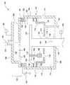
본 명세서에 개시된 실시예들은 반도체 기판을 프로세싱하기 위한 장치를 제공한다. 도 1은 일 실시예에 따른 장치(100)의 개략적인 단면도이다. 도 1의 장치(100)는 그 측벽에 기판 이송 개구(114)가 배치된 전도성 챔버 본체(164)를 구비한 프로세싱 챔버(104)를 포함한다. 기판 이송 개구(114)는 기판들이 프로세싱 챔버(104) 내외로 이송될 수 있도록 한다. 많은 실시예들에서, 로봇(미도시)과 같은 기판 핸들링 장치가 기판 이송 개구(114)를 통해 프로세싱 챔버(104)로 진입하여, 프로세싱 챔버(104) 내에 기판을 위치시키거나 프로세싱 챔버(104)로부터 기판을 제거한다.Embodiments disclosed herein provide an apparatus for processing a semiconductor substrate. 1 is a schematic cross-sectional view of an
챔버 본체(164)는 전도성 측벽(178)과 하부 벽체(146)를 포함하며, 이들은 알루미늄 또는 스테인리스 스틸, 또는 금속 또는 금속 합금과 같은 임의의 다른 전도성 물질일 수 있다. 챔버 본체(164)의 내면은 챔버 본체(164)에 대한 화학적 침식을 줄이기 위해 저항성 물질로 코팅될 수 있다. 제거가능한 라이너가 사용될 수도 있다. 코팅 또는 라이너는 금속 산화물과 같은 세라믹 물질, 예컨대, 알루미나 또는 이트리아, 또는 티타늄과 같은 저항성 금속, 또는 이들의 임의의 편리한 조합일 수 있다.
장치(100)는 챔버 내에 배치된 기판 지지체(106)를 더 포함한다. 기판 지지체(106)는 프로세싱을 위해 기판이 위에 배치될 수 있는 지지면(110)을 갖는다. 하나 또는 그 초과의 리프트 핀(108)들이 기판 지지체(106)를 통해 지지면(110)까지 연장하며, 지지면(110) 아래로 베이스(166)까지 연장한다. 기판 지지체(106)는 축부(122)를 가지며, 축부는 챔버 본체(164)의 하부 벽체(146)의 개구(144)를 통해 연장하여 액추에이터(미도시)에 커플링되고, 액추에이터는 지지면(110)이 하부 벽체(146)에 대해 근접하거나 멀어지도록 프로세싱 챔버(104) 내부에서 기판 지지체(106)를 움직인다. 지지면(110)이 하부 벽체(146)에 근접함에 따라, 리프트 핀(108)의 베이스(166)가 하부 벽체(146)에 접하게 되고, 리프트 핀(108)의 상부는 지지면(110) 위로 연장하게 된다. 리프트 핀(108)들이 지지면(110) 위로 연장될 때, 지지면(110) 위로 기판을 들어올리도록, 일반적으로, 복수의 리프트 핀(108)들이 마련된다. 도 1의 단면도에서는 오직 1개의 리프트 핀(108)만 볼 수 있다. 일반적으로, 기판 지지체(106)는 프로세싱 구역(112)을 포함하는 프로세싱 챔버(105)의 상부(168)와, 프로세싱 챔버(104)의 하부(170)를 규정한다.The
장치(100)는 프로세싱 챔버(104)의 하부(170) 내에 배치된 차폐 부재(116)를 더 포함한다. 차폐 부재(116)는 세라믹, 유리, 석영, 플라스틱, 또는 그들의 혼합물들, 그들의 화합물들 또는 그들의 조합들을 포함하는 유사한 물질들 같은, 단열 물질을 포함한다. 차폐 부재(116)는 하부 벽체(146)의 제 2 개구(120)를 관통하는 연장부(118)를 포함하며, 상기 연장부는 프로세싱 챔버(104) 내부에 당해 차폐 부재(116)를 위치시키기 위해 제 1 액추에이터(미도시)에 커플링된다. 차폐 부재(116)는 기판 이송 개구(114)를 통한 열손실을 방지하는 열적 차폐체를 프로세싱 구역(112)과 기판 이송 개구(114) 사이에 생성하며, 프로세싱시 프로세싱 챔버(104) 내에서의 열적 균일성을 향상시킨다. 일반적으로, 차폐 부재(116)는, 프로세싱 챔버(104)의 하부(170)에서 임의의 열손실 특징부로 인한 프로세싱 구역(112)의 열적 교란을 방지하기 위해, 프로세싱 챔버(104)의 전체 하부(170)를 차폐한다. 기판 로딩 또는 언로딩 작업시, 차폐 부재(116)와 기판 지지체(106)는 기판 이송 개구(114) 아래의 위치로 이동하여 지지면(110)에 대한 접근을 허용한다. 프로세싱시, 기판 지지체(106)는 지지면(110)을 프로세싱 구역(112)으로 이동시키고, 차폐 부재(116)는 프로세싱 챔버(104)의 측벽(178)을 따라 배치된 펌핑 플리넘(156)에 근접하는 위치로 이동한다.The
펌핑 플리넘(156)은 프로세싱 챔버의 측벽(178)을 따라 배치된 링형 채널이다. 펌핑 플리넘(156)의 내측부(158)의 개구(160)는 챔버의 프로세싱 구역(112)으로부터 채널로 프로세스 가스들을 받아들인다. 프로세스 가스들은 채널을 돌아 펌핑 플리넘(156)의 출입구(162)로 흐르며, 상기 출입구는 챔버(104)로부터 프로세스 가스들을 배출하기 위해 프로세싱 챔버(104)의 측벽(178)에 형성된 그와 유사한 출입구(154)와 결합되어 있다. 상기 개구(160)는 전체 펌핑 플리넘(156)을 따라 형성된 환형 그루브 또는 슬릿이거나, 펌핑 플리넘(156) 주변에 등간격으로 형성된 일련의 분리된 개구들일 수 있다. 개구(160)는 연속적이거나 불연속적일 수 있으며, 펌핑 플리넘(156)으로의 균일한 가스 흐름을 위한 압력 강하를 제공하는 크기일 수 있다.
차폐 부재(116)는 판부(172)와 벽부(174)를 포함한다. 판부는 기판 지지체(106)의 축부(122)를 수용하는 제 1 개구(176)와 리프트 핀(108)의 베이스부(166)를 수용하는 제 2 개구(124)를 갖는다. 기판을 프로세싱할 때, 열적 교란으로부터 프로세싱 구역(112)을 효과적으로 차폐하기 위해, 벽부(174)는 개구 또는 개구(160)들의 하부에 근접하여 위치된다. 대안적 실시예에서, 차폐 부재(116)는 벽부(174) 없이 형성될 수 있다. 그러한 실시예에서, 차폐 부재(116)는, 펌핑 플리넘(156)의 하면에 근접한 위치로 이동하는, 일부 실시예들에서, 펌핑 플리넘(156)의 하면에 접촉할 수 있는, 단열판일 수 있다.The
장치(100)는 덮개판(126)에 의해 프로세싱 챔버(104)의 측벽(178)에 커플링되는 덮개 조립체(102)를 더 포함한다. 덮개 조립체(102)는 함께 가스 박스(138)를 형성하는 배면 전극(184)과 면판(136)을 가진 가스 분배기(134)를 포함한다. 면판(136)은 프로세싱 구역(112)으로 프로세스 가스들을 받아들이는 복수의 개구(140)들을 갖는다. 가스 분배기(134)는 전도성이며, 알루미늄, 스테인리스 스틸, 티타늄, 또는 금속 또는 합금과 같은 다른 전도성 물질로 제조될 수 있다. 프로세싱 구역(112)을 대면하고 있는 면판(136)의 표면은 화학적 침식을 줄이기 위해 세라믹 또는 저항성 금속과 같은 저항성 물질로 코팅될 수 있다. 가스 분배기(134)는 가스 박스(138)에서 및/또는 프로세싱 구역(112)에서 이온화된 가스를 발생시키기 위해 RF 파워 소오스(148)에 커플링된다. 프로세싱 구역(112)에 노출되는 면판(136) 부분이 전체 프로세싱 구역(112)을 가로질러 균일하게 평탄하도록, 면판(136)은 측방향으로 프로세싱 구역(112)을 넘어서 연장한다. 평탄한 면판(136)은 가스 분배기(134)에 대한 RF 커플링에 의해 프로세싱 구역(112)에서 생성되는 전기장의 균일성을 향상시킨다.The
면판(136)은 면판(136)을 통한 열전도를 강화하는 두께로 형성된다. 강화된 열전도는 면판(136)에서의 온도 균일성을 향상시키고, 그에 따라 전체 프로세싱 구역(112)에서의 온도 균일성을 향상시킨다. 기판 지지체가 300℃ 내지 500℃의 온도로 가열되는 증착 프로세스에서, 알루미늄으로 제조되어 전술한 치수들을 가진 면판(136)은 면판의 중심 영역에서 면판의 주변 영역까지, 약 15℃ 미만과 같은, 약 20℃ 미만, 예컨대, 13℃의 온도차를 가질 것이다.The
덮개 조립체(102)는 절연체(132)에 의해 가스 분배기로부터 전기적으로 절연된 전극(130)을 더 포함한다. 전극(130)은 상기 절연체(132)와 제 2 절연체(128) 사이에 배치된 환형 전도성 부재이며, 상기 제 2 절연체는 프로세싱 챔버(104)의 측벽(178)으로부터 덮개 조립체(102)를 절연한다. 전극(130)은 환형, 링형 또는 토로이달형일 수 있으며, 일반적으로, 당해 전극(130)에 의해 생성되는 전기장의 균일성을 최대화하기 위해 균일한 단면 형상을 갖는다. 전극(130)은 DC 파워 소오스로서 도 1의 실시예에 도시된 전력 소오스(152)에 커플링되지만, 이는 RF 바이어스 소오스일 수도 있다. 전극(130)은 필요한 이온화된 가스 또는 플라즈마를 성형하기 위해 프로세싱 구역(112)에 전위가 발생될 수 있도록 한다. 전극(130)의 전위가 변화됨에 따라, 가스로부터의 이온들 또는 전자들이 전극(130)으로 점차 끌리게 되고, 기판 지지체(106)의 지지면(110)을 가로지르는 이온화된 가스 또는 플라즈마의 밀도 프로파일이 증착 균일성을 촉진하기 위해 조절될 수 있다.The
프로세싱 구역(112)은, 기판 지지체(106)의 지지면(110), 가스 분배기(134)의 면판(136), 및 2개의 절연체(132, 128)들과 전극(130)을 포함하는 측부 링 스택에 의해 규정된다. 프로세싱시, 기판 지지체(106)가 절연체(128) 및/또는 전극(130)에 근접한 위치로 이동하고, 지지면(110)은 프로세싱 구역(112)을 위한 플로어를 형성한다. 프로세스 가스들이 지지면(110)의 에지에서 프로세싱 구역을 빠져나와, 지지면(110) 아래에 이격되어 있는 펌핑 플리넘(156)을 향해 흐른다. 덮개 조립체(102) 속으로 프로세싱 구역(112)을 이동시킴으로써 챔버 본체(164)로부터 프로세싱 구역(112)을 멀리 위치시키면, 프로세스 가스들과 챔버 본체 표면들 간의 접촉을 줄여서, 챔버 본체 표면들에 대한 화학적 침식 속도를 저하시킨다. 또한, 전도성 챔버 측벽들에 대한 플라즈마 또는 이온화된 가스의 노출을 줄이면, 챔버 측벽에 대한 방전으로 인한 간헐적인 접지 가능성이 줄어든다.The
전극(130)은 전도성이며, 일반적으로, 금속 또는 금속 합금이다. 전극(130)이 프로세싱 구역(112)을 대면하고 프로세스 가스들에 노출되는 표면을 가진 링으로 도시되어 있으나, 2개의 절연체(128, 132)들 대신 연속적인 프로세스 대향면을 가진 단일의 절연체를 제공하고 그 단일의 절연체의 내부 채널에 전극(130)을 형성함으로써, 또는 그 단일의 절연체의 외측부 주위에 전극을 삽입하기 위한 채널을 형성함으로써, 프로세스 환경으로부터 전극이 차폐될 수 있다. 그러한 실시예들은 전극을 프로세스 환경에 노출시키지 않고 플라즈마 프로파일을 제어하기 위한 전위의 사용을 가능하게 할 것이다. 다른 실시예들에서, 프로세싱 환경을 대면하고 있는 전극(130)의 표면이 세라믹 또는 저항성 금속 같은 저항성 물질로 코팅될 수 있다.
기판 지지체(106)는, 기판 지지체(106)의 중심축(180)이 프로세싱 챔버(104)의 중심축(182)에 대해 실질적으로 평행하도록, 배향된다. 기판 지지체(106)는 축 평행(axis parallelism)에서 약 1% 미만까지, 약 0.1% 미만과 같이, 예컨대, 약 0.5% 미만으로, 또는 약 0.01 내지 약 1% 사이, 약 0.07%와 같이, 예컨대, 약 0.05% 내지 약 0.5%로 이탈을 제한하는 강성도를 갖는다. 따라서, 기판 지지체(106)는 이동거리당 약 0.01인치(in/in 단위) 이하, 약 0.0007in/in와 같이, 예컨대, 약 0.005in/in 미만으로 기울어진다.The
기판 지지체(106)의 강성도는 기판 지지체(106)의 지지면(110)과 가스 분배기(134)의 면판(136) 사이에 균일한 거리를 제공한다. 균일한 거리는 기판 지지체(106)의 지지면(110)과 면판(136) 사이에 형성되는 전기장의 균일성을 촉진하며, 프로세싱 구역(112) 전체에서의 플라즈마 밀도 균일성을 향상시킨다. 기판 지지체(106)는 프로세싱 구역(112)에서의 플라즈마 특성들의 제어를 용이하게 하기 위해 RF 파워 소오스(150)에도 커플링될 수 있다. 2개의 플라즈마 소오스(148, 150)들은, 예컨대, 프로세싱 구역(112)에서 다수의 종들의 이온화를 촉진하기 위해, 2개의 서로 다른 주파수들로 조정될 수 있다.The stiffness of the
기판 지지체(106)의 강성도는 축부(122)의 두께를 선택함으로써 선택될 수 있다. 많은 실시예들에서, 기판 지지체(106)의 축부(122)는 가스들, 액체들 또는 전기 요소들을 위한 다양한 유형들의 도관들을 포함한다. 축부(122)의 강성도는 축부(122)의 고체 부분들의 폭에 의해 주로 영향을 받는다. 따라서, 축부(122)의 전체적인 질량(general mass)을 늘리면, 그 강성도가 증가하게 될 것이다.The stiffness of the
도 1의 덮개 조립체(102), 기판 지지체(106) 및 차폐 부재(116)는 플라즈마 또는 열적 프로세싱을 위한 임의의 프로세싱 챔버와 함께 사용될 수 있다. 덮개 조립체(102), 기판 지지체(106) 및 차폐 부재(116)와 함께 유리하게 사용될 수 있는 플라즈마 프로세싱 챔버의 일 예는 캘리포니아주 산타 클라라에 소재한 어플라이드 머티어리얼 인코포레이티드로부터 입수할 수 있는 PRODUCER® 플랫폼 및 챔버들이다. 다른 제조사들의 챔버들도 전술한 부품들과 함께 사용될 수 있다.The
도 2는 다른 실시예에 따른 방법(200)을 요약한 흐름도이다. 도 2의 방법은, 도 1의 장치(100)의 실시예들을 포함하여, 플라즈마 프로세싱을 위해 적절하게 구성된 임의의 기판 프로세싱 챔버를 사용하여 실시될 수 있다. 단계 202에서, 프로세싱 챔버 내의 기판 지지체 상에 기판을 배치한다. 단계 204에서, 상기 챔버에 덮개를 제공하되, 상기 덮개는 전도성 가스 분배판과 상기 가스 분배판 아래에서 당해 덮개의 측벽 주위에 배치된 전극을 포함한다. 상기 전극은 절연체 링에 의해 가스 분배판으로부터 절연될 수 있으며, 이들 모두는 환형일 수 있다.2 is a flow diagram summarizing a
단계 206에서, 프로세싱을 위해 전극 부근에 기판을 위치시킨다. 기판 지지체는 임의의 편리한 방식으로 이동될 수 있다. 일부 실시예들에서, 기판 지지체와 가스 분배판은 다른 챔버 부품들에 대한 화학적 침식과 플라즈마 아킹이 발생하는 경우를 줄이기 위해 다른 챔버 부품들로부터 멀리 유지되는 프로세싱 영역을 규정한다. 일부 실시예들에서, 덮개와 챔버 본체 사이에 제 2 절연체 링이 제공될 수 있다. 일반적으로, 절연체 링은 프로세싱 구역을 위해 화학적으로 저항성이 있는 측벽을 형성한다. 일부 실시예들에서, 가스 분배판과 전극은 저항성 물질로 코팅될 수도 있다.In
기판은, 기판의 에지가 전극에 근접하도록, 위치된다. 기판 에지로부터 전극까지의 거리는, 일반적으로, 약 10㎜ 미만일 것이다. 그 거리는 약 2 내지 약 10㎜, 약 6㎜와 같이, 예컨대, 약 4㎜ 내지 약 6㎜일 수 있다. 일부 실시예들에서, 기판 에지와 전극 사이의 갭은 기판 에지를 따라 모든 지점들에서 유동 균일성을 제공하는 크기일 수 있다.The substrate is positioned so that the edge of the substrate is close to the electrode. The distance from the substrate edge to the electrode will generally be less than about 10 mm. The distance may be, for example, about 4 mm to about 6 mm, such as about 2 to about 10 mm, about 6 mm. In some embodiments, the gap between the substrate edge and the electrode can be sized to provide flow uniformity at all points along the substrate edge.
단계 208에서, 기판 지지체와 가스 분배판에 의해 규정되는 프로세싱 영역에 혼합물일 수 있는 프로세스 가스를 제공한다. 일반적으로, 프로세스 가스는 가스 분배판의 개구들을 통해 흐르며, 이들은 원하는 유동 특성들을 구현하기 위해 임의의 편리한 방식으로 성형될 수 있다. 단계 210에서, 가스 분배판에 RF 파워를 커플링함으로써, 프로세싱 영역 내의 프로세스 가스로부터 플라즈마를 형성한다. RF 파워는 기판 상에 전기적 바이어스를 생성하거나 프로세스 가스의 이온화를 더 조장하기 위해 기판 지지체에 커플링될 수도 있다.In
단계 212에서, 기판 지지체를 가로질러 플라즈마 밀도 프로파일을 제어하기 위해 전극에 전위를 인가한다. 가스 분배판과 기판 지지체에 대한 전극의 전위를 조절하면, 프로세싱 영역 또는 챔버의 측벽과 플라즈마 시스(sheath) 사이의 거리가 조절됨으로써, 플라즈마에 대한 기판의 노출이 기판의 에지로 제한될 수 있다. 다양한 전도성 부품들의 구조적 불연속성들을 최소화하는 것도 프로세싱 영역에서 플라즈마 밀도 균일성 제어를 개선한다.In
단계 214에서, 챔버의 하부에서 기판 지지체 아래에 위치된 펌핑 플리넘을 통해 배기 가스들을 균일하게 배기한다. 펌핑 플리넘은, 기판 지지체를 가로질러 그 에지를 돌아 챔버의 하부를 거쳐 당해 펌핑 플리넘 속으로, 균일한 가스 흐름을 제공하도록 구성되어 있다. 기판 지지체 아래에 펌핑 플리넘을 제공하면, 펌핑 플리넘의 작동으로 인해 가스 흐름 이상이 줄어든다. 펌핑 플리넘으로부터 소정 거리만큼 프로세싱 챔버의 덮개를 이격시킨 다음, 프로세싱을 위해 덮개에 근접하여 기판을 위치시킴으로써, 프로세싱 영역과 펌핑 플리넘 사이의 거리가 조절될 수 있다.In
도 2의 방법(200)은 용량성 플라즈마 챔버에서 실시되는 임의의 플라즈마 프로세스를 위해 사용될 수 있다. 예컨대, 플라즈마 CVD에 의해 실리콘, 산소, 탄소, 질소 또는 다른 원소들을 함유한 층들이 형성되는 증착 프로세스들이 상기 방법(200)의 균일성 강화로 인한 이익을 향유할 수 있다. 실리콘, 탄소, 산소, 질소 또는 다른 원소들을 포함하는 가스들과 아울러, 아르곤 또는 헬륨과 같은 불활성 또는 비반응성 가스들을 포함하는 프로세스 가스로부터 플라즈마가 형성될 수 있다. 약 +30V 내지 약 +70V와 같은, 약 +10V 내지 +100V, 예컨대, +50V의 DC 전위가 전자들을 끌어당기기 위해 전극에 인가될 수 있으며, 상기 전자들은 전극을 향하여 팽창하는 플라즈마 시스를 형성한다.The
일부 실시예들에서, 상기 방법(200)은 열 손실되기 쉬운 프로세싱 챔버의 부분들을 열적으로 차폐하는 단계를 더 포함할 수 있다. 예컨대, 챔버의 하나의 벽체에 형성된 접근 포트를 차폐하기 위해 챔버의 하부에 열 차폐체가 배치될 수 있다. 열 차폐체는 챔버 벽체의 임의의 차폐된 부분들을 통한 챔버로부터의 열손실을 줄인다.In some embodiments, the
도 3은 다른 실시예에 따른 장치(300)의 개략적인 평면도이다. 장치(300)는 복수의 프로세싱 챔버(302)들, 기판 이송 챔버(304), 기판 핸들러(310), 및 하나 또는 그 초과의 로드 락 챔버(306)들을 포함한다. 기판 핸들러(310)는 임의의 적당하게 설계된 로봇일 수 있다. 일 실시예에서, 기판 핸들러(310)는 2개의 근접한 프로세싱 챔버(302)들에 대해 동시에 접근하는 2개의 링크된 탠덤 블레이드 로봇들을 포함한다. 상기 장치(300)의 프로세싱 챔버(302)들 중 하나 또는 그 초과의 프로세싱 챔버들은 상기 챔버(100)와 유사할 수 있다. 각각의 프로세싱 챔버(302)들은 도 1의 장치와 관련하여 전술한 바와 같은 튜닝 전극(130)을 갖는다. 상기 장치(300)는 도 1과 관련하여 전술한 펌핑 플리넘(156)과 같은 펌핑 플리넘과 각각 유체 소통하는 복수의 가스 배기 도관(308)들을 또한 포함하고, 하나의 도관(308)이 각 쌍의 프로세싱 챔버(302)들을 담당한다. 상기 챔버(100)와 같은 플라즈마 프로세싱 챔버들과 아울러, 다른 유형들의 챔버들이 도 3의 장치(300)에 포함될 수 있다. 예컨대, 프로세싱 챔버(302)들 중 하나 또는 그 초과의 프로세싱 챔버들이 열처리 챔버, 세척 챔버, 자외선 처리 챔버, 냉각 또는 휴지 챔버일 수 있다.3 is a schematic plan view of an
이상의 설명은 본 발명의 실시예들에 관한 것이나, 본 발명의 기본적인 범위를 벗어나지 않고 다른 추가적인 실시예들이 안출될 수 있다.Although the above description relates to embodiments of the present invention, other additional embodiments may be devised without departing from the basic scope of the present invention.
Claims (16)
Translated fromKorean기판 이송 개구를 구비한 챔버 본체를 가진 프로세싱 챔버;
상기 프로세싱 챔버 내에 배치되고, 상기 프로세싱 챔버의 상부 및 상기 프로세싱 챔버의 하부를 정의하는 기판 지지체;
RF 파워에 커플링된 전도성 가스 분배기 및 상기 전도성 가스 분배기로부터 절연된 전력공급된(powered) 전극을 포함하는 덮개 조립체; 및
상기 프로세싱 챔버의 하부 내에 배치된 차폐 부재 ― 상기 차폐 부재는 상기 프로세싱 챔버의 외부에 있는 상기 차폐 부재의 연장부에 의해 상기 프로세싱 챔버의 내부에 위치될 수 있음(positionable) ―
를 포함하는,
반도체 기판을 프로세싱하기 위한 장치.An apparatus for processing a semiconductor substrate,
A processing chamber having a chamber body having a substrate transfer opening;
A substrate support disposed within the processing chamber and defining an upper portion of the processing chamber and a lower portion of the processing chamber;
A lid assembly comprising a conductive gas distributor coupled to RF power and a powered electrode insulated from the conductive gas distributor; And
A shield member disposed within the bottom of the processing chamber, wherein the shield member may be positioned inside the processing chamber by an extension of the shield member external to the processing chamber.
/ RTI >
An apparatus for processing a semiconductor substrate.
상기 덮개 조립체는 기판 프로세싱 구역을 더 포함하는,
반도체 기판을 프로세싱하기 위한 장치.The method of claim 1,
The lid assembly further comprises a substrate processing region,
An apparatus for processing a semiconductor substrate.
상기 차폐 부재는 기판 프로세싱 위치와 기판 이송 위치 사이에서 이동가능하며, 상기 차폐체가 상기 기판 프로세싱 위치에 위치되는 경우에, 상기 차폐체는 상기 기판 이송 개구를 덮는,
반도체 기판을 프로세싱하기 위한 장치.The method of claim 1,
The shield member is movable between a substrate processing position and a substrate transfer position, and when the shield is positioned at the substrate processing position, the shield covers the substrate transfer opening,
An apparatus for processing a semiconductor substrate.
상기 기판 지지체는 약 0.1% 미만 기울어져 있는,
반도체 기판을 프로세싱하기 위한 장치.The method of claim 1,
The substrate support is tilted less than about 0.1%,
An apparatus for processing a semiconductor substrate.
상기 덮개 조립체는 상기 전력공급된 전극 근처의 프로세싱 구역을 더 포함하고, 상기 차폐 부재는 기판 프로세싱 위치와 기판 이송 위치 사이에서 이동가능하며, 상기 차폐체가 상기 기판 프로세싱 위치에 위치되는 경우에, 상기 차폐체는 상기 기판 이송 개구를 덮는,
반도체 기판을 프로세싱하기 위한 장치.The method of claim 1,
The lid assembly further includes a processing region near the powered electrode, wherein the shield member is movable between a substrate processing position and a substrate transfer position, when the shield is positioned at the substrate processing position, the shield Covering the substrate transfer opening,
An apparatus for processing a semiconductor substrate.
상기 차폐 부재는 유전체 물질을 포함하며, 상기 덮개 조립체는 상기 전력공급된 전극과 상기 전도성 가스 분배기 사이, 그리고 상기 전력공급된 전극과 상기 챔버 본체 사이에 아이솔레이터(isolator)를 더 포함하는,
반도체 기판을 프로세싱하기 위한 장치.The method of claim 5, wherein
The shielding member comprises a dielectric material, the lid assembly further comprising an isolator between the powered electrode and the conductive gas distributor and between the powered electrode and the chamber body.
An apparatus for processing a semiconductor substrate.
상기 챔버 본체의 벽체 주위에 배치되고, 상면과 하면을 구비한 환형 개구를 포함한 펌핑 플리넘을 더 포함하며, 상기 차폐 부재가 기판 프로세싱 위치에 있는 경우에, 상기 차폐 부재의 상면은 상기 펌핑 플리넘의 하면과 실질적으로 평탄한(even),
반도체 기판을 프로세싱하기 위한 장치.The method of claim 1,
A pumping plenum disposed around the wall of the chamber body and including an annular opening having an upper surface and a lower surface, wherein when the shielding member is in a substrate processing position, the upper surface of the shielding member is formed of the pumping plenum. Substantially even with the bottom surface,
An apparatus for processing a semiconductor substrate.
상기 기판 이송 개구는 상기 펌핑 플리넘 아래에 있으며, 상기 차폐 부재가 기판 이송 위치에 위치되는 경우에, 상기 차폐 부재는 상기 기판 이송 개구를 노출시키는,
반도체 기판을 프로세싱하기 위한 장치.The method of claim 7, wherein
The substrate transfer opening is below the pumping plenum, and when the shield member is positioned at the substrate transfer position, the shield member exposes the substrate transfer opening,
An apparatus for processing a semiconductor substrate.
배면 전극, 가스 박스 및 면판을 가진 가스 분배기;
상기 가스 분배기의 면판으로부터 절연체 링에 의해 분리된 환형 튜닝 전극; 및
상기 프로세싱 챔버의 측벽에 커플링되고, 상기 튜닝 전극으로부터 아이솔레이터에 의해 분리된 덮개판을 포함하는,
반도체 프로세싱 챔버를 위한 덮개 조립체.A lid assembly for a semiconductor processing chamber,
A gas distributor having a back electrode, a gas box and a face plate;
An annular tuning electrode separated by an insulator ring from the face plate of the gas distributor; And
A cover plate coupled to the sidewall of the processing chamber and separated by an isolator from the tuning electrode,
Lid assembly for semiconductor processing chamber.
상기 환형 튜닝 전극 근처의 기판 프로세싱 구역을 더 포함하는,
반도체 프로세싱 챔버를 위한 덮개 조립체.The method of claim 9,
Further comprising a substrate processing region near the annular tuning electrode,
Lid assembly for semiconductor processing chamber.
상기 가스 분배기 및 상기 환형 튜닝 전극은 각각 전력의 소오스에 커플링되는,
반도체 프로세싱 챔버를 위한 덮개 조립체.The method of claim 9,
The gas distributor and the annular tuning electrode are each coupled to a source of power;
Lid assembly for semiconductor processing chamber.
상기 가스 분배기는 RF 파워의 소오스에 커플링되고, 상기 환형 튜닝 전극은 DC 파워의 소오스에 커플링되는,
반도체 프로세싱 챔버를 위한 덮개 조립체.The method of claim 11,
The gas distributor is coupled to a source of RF power and the annular tuning electrode is coupled to a source of DC power
Lid assembly for semiconductor processing chamber.
상기 프로세싱 챔버의 단면 형상과 유사한 형상을 가진 판;
상기 프로세싱 챔버 내에 배치된 기판 지지체의 축부를 위한, 상기 판에 있는 개구;
상기 기판 지지체의 리프트 핀부를 위한 상기 판에 있는 개구; 및
상기 판에 부착되며, 상기 프로세싱 챔버 내부에서의 기판 이송 위치와 기판 프로세싱 위치 사이에서 상기 차폐체를 이동시키기 위해 상기 프로세싱 챔버의 외부로 연장하는 연장부
를 포함하는,
반도체 프로세싱 챔버를 위한 차폐체.As a shield for a semiconductor processing chamber,
A plate having a shape similar to a cross-sectional shape of the processing chamber;
An opening in the plate for an axis of a substrate support disposed in the processing chamber;
An opening in the plate for a lift pin portion of the substrate support; And
An extension attached to the plate and extending out of the processing chamber to move the shield between a substrate transfer position within the processing chamber and a substrate processing position
/ RTI >
Shield for semiconductor processing chamber.
상기 판은 단열(thermally insulating) 물질을 포함하며, 상기 판의 중심으로부터 에지까지의 거리는 상기 프로세싱 챔버의 중심축으로부터 상기 프로세싱 챔버의 벽체 주위에 배치된 펌핑 플리넘의 내측 에지까지의 거리와 실질적으로 동일한,
반도체 프로세싱 챔버를 위한 차폐체.The method of claim 13,
The plate comprises a thermally insulating material, wherein the distance from the center to the edge of the plate is substantially the distance from the central axis of the processing chamber to the inner edge of the pumping plenum disposed around the wall of the processing chamber. same,
Shield for semiconductor processing chamber.
상기 판의 에지로부터 연장하는 벽체 및 상기 프로세싱 챔버 내부에서 상기 차폐체를 이동시키기 위해 상기 연장부에 커플링된 액추에이터를 더 포함하는,
반도체 프로세싱 챔버를 위한 차폐체.15. The method of claim 14,
And an actuator coupled to the extension for moving the shield within the wall and the wall extending from the edge of the plate,
Shield for semiconductor processing chamber.
프로세싱 챔버 내의 기판 지지체 상에 상기 기판을 배치하는 단계;
상기 기판 지지체의 반대측에 있는 전도성 가스 분배기에 RF 파워를 커플링시키는 단계;
상기 전도성 가스 분배기 근처의 상기 챔버의 측벽 내에 전극을 제공하는 단계;
상기 전극 근처의 프로세싱 위치로 상기 기판 지지체를 이동시키는 단계;
상기 전도성 가스 분배기와 상기 기판 지지체 사이의 프로세싱 영역으로 상기 가스 분배기를 통해 프로세싱 가스를 유동시키는 단계;
상기 프로세싱 가스로부터 플라즈마를 형성하는 단계; 및
상기 전극에 전위를 인가하여 상기 플라즈마를 성형하는 단계
를 포함하는,
기판을 프로세싱하기 위한 방법.A method for processing a substrate,
Placing the substrate on a substrate support in a processing chamber;
Coupling RF power to a conductive gas distributor opposite the substrate support;
Providing an electrode in a sidewall of the chamber near the conductive gas distributor;
Moving the substrate support to a processing position near the electrode;
Flowing a processing gas through the gas distributor to a processing region between the conductive gas distributor and the substrate support;
Forming a plasma from the processing gas; And
Shaping the plasma by applying a potential to the electrode;
/ RTI >
A method for processing a substrate.
Applications Claiming Priority (3)
| Application Number | Priority Date | Filing Date | Title |
|---|---|---|---|
| US33409310P | 2010-05-12 | 2010-05-12 | |
| US61/334,093 | 2010-05-12 | ||
| PCT/US2011/035534WO2011143062A2 (en) | 2010-05-12 | 2011-05-06 | Confined process volume pecvd chamber |
Publications (2)
| Publication Number | Publication Date |
|---|---|
| KR20130111221Atrue KR20130111221A (en) | 2013-10-10 |
| KR101924488B1 KR101924488B1 (en) | 2018-12-03 |
Family
ID=44914910
Family Applications (1)
| Application Number | Title | Priority Date | Filing Date |
|---|---|---|---|
| KR1020127032439AActiveKR101924488B1 (en) | 2010-05-12 | 2011-05-06 | Confined process volume pecvd chamber |
Country Status (6)
| Country | Link |
|---|---|
| US (1) | US8778813B2 (en) |
| JP (1) | JP2013526778A (en) |
| KR (1) | KR101924488B1 (en) |
| CN (1) | CN102884610A (en) |
| TW (1) | TWI549208B (en) |
| WO (1) | WO2011143062A2 (en) |
Cited By (2)
| Publication number | Priority date | Publication date | Assignee | Title |
|---|---|---|---|---|
| KR20160076456A (en)* | 2014-12-22 | 2016-06-30 | 어플라이드 머티어리얼스, 인코포레이티드 | Process kit for a high throughput processing chamber |
| KR20210008876A (en)* | 2016-11-15 | 2021-01-25 | 어플라이드 머티어리얼스, 인코포레이티드 | Dynamic phased array plasma source for complete plasma coverage of a moving substrate |
Families Citing this family (34)
| Publication number | Priority date | Publication date | Assignee | Title |
|---|---|---|---|---|
| US8647446B2 (en)* | 2011-12-07 | 2014-02-11 | Intermolecular, Inc. | Method and system for improving performance and preventing corrosion in multi-module cleaning chamber |
| JP6545460B2 (en) | 2012-02-29 | 2019-07-17 | アプライド マテリアルズ インコーポレイテッドApplied Materials,Incorporated | Abatement and stripping process chamber in load lock configuration |
| WO2014052228A1 (en)* | 2012-09-26 | 2014-04-03 | Applied Materials, Inc. | Bottom and side plasma tuning having closed loop control |
| WO2014052301A1 (en)* | 2012-09-26 | 2014-04-03 | Applied Materials, Inc. | Controlling temperature in substrate processing systems |
| US9157730B2 (en) | 2012-10-26 | 2015-10-13 | Applied Materials, Inc. | PECVD process |
| KR101443792B1 (en)* | 2013-02-20 | 2014-09-26 | 국제엘렉트릭코리아 주식회사 | Gas Phase Etcher Apparatus |
| KR101384353B1 (en)* | 2013-02-20 | 2014-04-14 | 국제엘렉트릭코리아 주식회사 | Substrate processing apparatus |
| KR20150131095A (en)* | 2013-03-15 | 2015-11-24 | 어플라이드 머티어리얼스, 인코포레이티드 | Apparatus and method for tuning a plasma profile using a tuning ring in a processing chamber |
| US10032608B2 (en) | 2013-03-27 | 2018-07-24 | Applied Materials, Inc. | Apparatus and method for tuning electrode impedance for high frequency radio frequency and terminating low frequency radio frequency to ground |
| CN104217914B (en)* | 2013-05-31 | 2016-12-28 | 中微半导体设备(上海)有限公司 | Plasma processing apparatus |
| CN104952762A (en)* | 2014-03-27 | 2015-09-30 | 北京北方微电子基地设备工艺研究中心有限责任公司 | Cooling chamber and semiconductor processing equipment |
| GB201504202D0 (en) | 2015-03-12 | 2015-04-29 | Spts Technologies Ltd | PE-CVD apparatus and method |
| US10354841B2 (en)* | 2015-04-07 | 2019-07-16 | Tokyo Electron Limited | Plasma generation and control using a DC ring |
| KR102678733B1 (en)* | 2015-12-04 | 2024-06-26 | 어플라이드 머티어리얼스, 인코포레이티드 | Advanced coating methods and materials to prevent HDP-CVD chamber arcing |
| EP3512978A4 (en)* | 2016-09-16 | 2020-05-13 | Picosun Oy | Apparatus and methods for atomic layer deposition |
| US20180294139A1 (en)* | 2017-04-07 | 2018-10-11 | Applied Materials, Inc. | Gas phase particle reduction in pecvd chamber |
| CN109023310B (en)* | 2017-06-12 | 2022-08-26 | 应用材料公司 | Method and apparatus for semiconductor processing chamber isolation for reduced particle and improved uniformity |
| KR20200139841A (en)* | 2018-05-03 | 2020-12-14 | 어플라이드 머티어리얼스, 인코포레이티드 | Universal adjustable blocker plate for tuning flow distribution |
| CN110484895B (en)* | 2018-05-14 | 2021-01-08 | 北京北方华创微电子装备有限公司 | Chamber assembly and reaction chamber |
| US11434569B2 (en)* | 2018-05-25 | 2022-09-06 | Applied Materials, Inc. | Ground path systems for providing a shorter and symmetrical ground path |
| US20200058539A1 (en)* | 2018-08-17 | 2020-02-20 | Applied Materials, Inc. | Coating material for processing chambers |
| CN111326391B (en)* | 2018-12-17 | 2023-01-24 | 中微半导体设备(上海)股份有限公司 | Plasma processing apparatus |
| GB2582948B (en)* | 2019-04-10 | 2021-12-08 | Thermo Fisher Scient Bremen Gmbh | Plasma source chamber for a spectrometer |
| WO2020231615A1 (en)* | 2019-05-15 | 2020-11-19 | Applied Materials, Inc. | Process chamber with reduced plasma arc |
| KR102640172B1 (en) | 2019-07-03 | 2024-02-23 | 삼성전자주식회사 | Processing apparatus for a substrate and method of driving the same |
| CN112538618B (en)* | 2019-09-20 | 2022-02-22 | 江苏菲沃泰纳米科技股份有限公司 | Moving electrode device, movable support device and application |
| US11555247B2 (en) | 2019-09-20 | 2023-01-17 | Jiangsu Favored Nanotechnology Co., Ltd. | Coating apparatus and movable electrode arrangement, movable support arrangement, and application thereof |
| JP7407645B2 (en)* | 2020-04-03 | 2024-01-04 | 東京エレクトロン株式会社 | plasma processing equipment |
| JP7468246B2 (en)* | 2020-08-21 | 2024-04-16 | ウシオ電機株式会社 | Extreme ultraviolet light source device |
| US12020957B2 (en) | 2020-08-31 | 2024-06-25 | Applied Materials, Inc. | Heater assembly with process gap control for batch processing chambers |
| CN112509903B (en)* | 2020-12-17 | 2025-05-16 | 上海谙邦半导体设备有限公司 | Plasma processing device |
| US20220328293A1 (en)* | 2021-04-13 | 2022-10-13 | Applied Materials, Inc. | Isolator for processing chambers |
| CN115172129A (en)* | 2022-06-30 | 2022-10-11 | 大族激光科技产业集团股份有限公司 | Vapor deposition device and vapor deposition equipment |
| US20250299926A1 (en)* | 2024-03-22 | 2025-09-25 | Applied Materials, Inc. | Biasable gas distribution plate |
Family Cites Families (14)
| Publication number | Priority date | Publication date | Assignee | Title |
|---|---|---|---|---|
| US5846332A (en)* | 1996-07-12 | 1998-12-08 | Applied Materials, Inc. | Thermally floating pedestal collar in a chemical vapor deposition chamber |
| US5800621A (en)* | 1997-02-10 | 1998-09-01 | Applied Materials, Inc. | Plasma source for HDP-CVD chamber |
| US6079356A (en) | 1997-12-02 | 2000-06-27 | Applied Materials, Inc. | Reactor optimized for chemical vapor deposition of titanium |
| US6916399B1 (en)* | 1999-06-03 | 2005-07-12 | Applied Materials Inc | Temperature controlled window with a fluid supply system |
| US7001491B2 (en)* | 2003-06-26 | 2006-02-21 | Tokyo Electron Limited | Vacuum-processing chamber-shield and multi-chamber pumping method |
| JP2007012724A (en)* | 2005-06-29 | 2007-01-18 | Matsushita Electric Ind Co Ltd | Plasma processing apparatus and processing method |
| KR100717286B1 (en)* | 2006-04-21 | 2007-05-15 | 삼성전자주식회사 | Formation method of phase change material layer, formation method of phase change memory device and phase change memory device using the method |
| US7972470B2 (en)* | 2007-05-03 | 2011-07-05 | Applied Materials, Inc. | Asymmetric grounding of rectangular susceptor |
| JP4470970B2 (en)* | 2007-07-31 | 2010-06-02 | 東京エレクトロン株式会社 | Plasma processing equipment |
| KR101489963B1 (en)* | 2007-12-13 | 2015-02-04 | 한국에이에스엠지니텍 주식회사 | Thin film deposition apparatus and deposition method using the same |
| KR101404010B1 (en)* | 2008-03-06 | 2014-06-12 | 주성엔지니어링(주) | Substrate edge etching apparatus and substrate edge etching method using the same |
| US20090236214A1 (en)* | 2008-03-20 | 2009-09-24 | Karthik Janakiraman | Tunable ground planes in plasma chambers |
| US8317969B2 (en)* | 2008-03-25 | 2012-11-27 | Tokyo Electron Limited | Plasma processing apparatus |
| US7699935B2 (en)* | 2008-06-19 | 2010-04-20 | Applied Materials, Inc. | Method and system for supplying a cleaning gas into a process chamber |
- 2011
- 2011-05-06WOPCT/US2011/035534patent/WO2011143062A2/enactiveApplication Filing
- 2011-05-06CNCN2011800233881Apatent/CN102884610A/enactivePending
- 2011-05-06KRKR1020127032439Apatent/KR101924488B1/enactiveActive
- 2011-05-06USUS13/102,846patent/US8778813B2/enactiveActive
- 2011-05-06JPJP2013510179Apatent/JP2013526778A/ennot_activeWithdrawn
- 2011-05-12TWTW100116710Apatent/TWI549208B/enactive
Cited By (2)
| Publication number | Priority date | Publication date | Assignee | Title |
|---|---|---|---|---|
| KR20160076456A (en)* | 2014-12-22 | 2016-06-30 | 어플라이드 머티어리얼스, 인코포레이티드 | Process kit for a high throughput processing chamber |
| KR20210008876A (en)* | 2016-11-15 | 2021-01-25 | 어플라이드 머티어리얼스, 인코포레이티드 | Dynamic phased array plasma source for complete plasma coverage of a moving substrate |
Also Published As
| Publication number | Publication date |
|---|---|
| JP2013526778A (en) | 2013-06-24 |
| WO2011143062A2 (en) | 2011-11-17 |
| US8778813B2 (en) | 2014-07-15 |
| TW201207975A (en) | 2012-02-16 |
| KR101924488B1 (en) | 2018-12-03 |
| WO2011143062A3 (en) | 2012-05-10 |
| TWI549208B (en) | 2016-09-11 |
| US20110294303A1 (en) | 2011-12-01 |
| CN102884610A (en) | 2013-01-16 |
Similar Documents
| Publication | Publication Date | Title |
|---|---|---|
| KR101924488B1 (en) | Confined process volume pecvd chamber | |
| KR100635975B1 (en) | Apparatus and method for plasma treatment | |
| US8592712B2 (en) | Mounting table structure and plasma film forming apparatus | |
| KR100900585B1 (en) | Focus ring and plasma processing apparatus | |
| CN109844176B (en) | Pin lifter assembly with small clearance | |
| KR102218686B1 (en) | Plasma processing apparatus | |
| KR20190005750A (en) | Plasma processing apparatus | |
| KR20200054330A (en) | Bottom and middle edge rings | |
| KR101898079B1 (en) | Plasma processing apparatus | |
| KR102794111B1 (en) | Plasma treatment device | |
| US7897009B2 (en) | Plasma processing apparatus | |
| CN112863985A (en) | Plasma processing apparatus | |
| CN112534558B (en) | Preventing deposition on pedestals during semiconductor substrate processing | |
| TW202204677A (en) | Lid stack for high frequency processing | |
| US10301718B2 (en) | Asymmetric pedestal/carrier ring arrangement for edge impedance modulation | |
| KR102799000B1 (en) | Plasma processing apparatus | |
| KR20250002447A (en) | Showerhead assembly having a heated showerhead | |
| CN111326395A (en) | Plasma processing method and plasma processing apparatus | |
| JP7747417B2 (en) | Plasma processing apparatus and method for manufacturing the same | |
| JP2006128529A (en) | Depositing equipment, depositing method, and storage medium | |
| JP2002343779A (en) | Heat-treating equipment |
Legal Events
| Date | Code | Title | Description |
|---|---|---|---|
| PA0105 | International application | St.27 status event code:A-0-1-A10-A15-nap-PA0105 | |
| P11-X000 | Amendment of application requested | St.27 status event code:A-2-2-P10-P11-nap-X000 | |
| P13-X000 | Application amended | St.27 status event code:A-2-2-P10-P13-nap-X000 | |
| PG1501 | Laying open of application | St.27 status event code:A-1-1-Q10-Q12-nap-PG1501 | |
| PA0201 | Request for examination | St.27 status event code:A-1-2-D10-D11-exm-PA0201 | |
| P22-X000 | Classification modified | St.27 status event code:A-2-2-P10-P22-nap-X000 | |
| P22-X000 | Classification modified | St.27 status event code:A-2-2-P10-P22-nap-X000 | |
| D13-X000 | Search requested | St.27 status event code:A-1-2-D10-D13-srh-X000 | |
| D14-X000 | Search report completed | St.27 status event code:A-1-2-D10-D14-srh-X000 | |
| E902 | Notification of reason for refusal | ||
| PE0902 | Notice of grounds for rejection | St.27 status event code:A-1-2-D10-D21-exm-PE0902 | |
| P11-X000 | Amendment of application requested | St.27 status event code:A-2-2-P10-P11-nap-X000 | |
| P13-X000 | Application amended | St.27 status event code:A-2-2-P10-P13-nap-X000 | |
| E90F | Notification of reason for final refusal | ||
| PE0902 | Notice of grounds for rejection | St.27 status event code:A-1-2-D10-D21-exm-PE0902 | |
| P11-X000 | Amendment of application requested | St.27 status event code:A-2-2-P10-P11-nap-X000 | |
| P13-X000 | Application amended | St.27 status event code:A-2-2-P10-P13-nap-X000 | |
| E701 | Decision to grant or registration of patent right | ||
| PE0701 | Decision of registration | St.27 status event code:A-1-2-D10-D22-exm-PE0701 | |
| GRNT | Written decision to grant | ||
| PR0701 | Registration of establishment | St.27 status event code:A-2-4-F10-F11-exm-PR0701 | |
| PR1002 | Payment of registration fee | St.27 status event code:A-2-2-U10-U12-oth-PR1002 Fee payment year number:1 | |
| PG1601 | Publication of registration | St.27 status event code:A-4-4-Q10-Q13-nap-PG1601 | |
| PR1001 | Payment of annual fee | St.27 status event code:A-4-4-U10-U11-oth-PR1001 Fee payment year number:4 | |
| PR1001 | Payment of annual fee | St.27 status event code:A-4-4-U10-U11-oth-PR1001 Fee payment year number:5 | |
| PR1001 | Payment of annual fee | St.27 status event code:A-4-4-U10-U11-oth-PR1001 Fee payment year number:6 | |
| PR1001 | Payment of annual fee | St.27 status event code:A-4-4-U10-U11-oth-PR1001 Fee payment year number:7 | |
| R17-X000 | Change to representative recorded | St.27 status event code:A-5-5-R10-R17-oth-X000 |